WO2011158666A1 - 接続構造体の製造方法 - Google Patents
接続構造体の製造方法 Download PDFInfo
- Publication number
- WO2011158666A1 WO2011158666A1 PCT/JP2011/062779 JP2011062779W WO2011158666A1 WO 2011158666 A1 WO2011158666 A1 WO 2011158666A1 JP 2011062779 W JP2011062779 W JP 2011062779W WO 2011158666 A1 WO2011158666 A1 WO 2011158666A1
- Authority
- WO
- WIPO (PCT)
- Prior art keywords
- heating
- anisotropic conductive
- temperature
- conductive adhesive
- electric element
- Prior art date
Links
Images
Classifications
-
- H—ELECTRICITY
- H01—ELECTRIC ELEMENTS
- H01R—ELECTRICALLY-CONDUCTIVE CONNECTIONS; STRUCTURAL ASSOCIATIONS OF A PLURALITY OF MUTUALLY-INSULATED ELECTRICAL CONNECTING ELEMENTS; COUPLING DEVICES; CURRENT COLLECTORS
- H01R43/00—Apparatus or processes specially adapted for manufacturing, assembling, maintaining, or repairing of line connectors or current collectors or for joining electric conductors
- H01R43/02—Apparatus or processes specially adapted for manufacturing, assembling, maintaining, or repairing of line connectors or current collectors or for joining electric conductors for soldered or welded connections
- H01R43/0242—Apparatus or processes specially adapted for manufacturing, assembling, maintaining, or repairing of line connectors or current collectors or for joining electric conductors for soldered or welded connections comprising means for controlling the temperature, e.g. making use of the curie point
-
- C—CHEMISTRY; METALLURGY
- C09—DYES; PAINTS; POLISHES; NATURAL RESINS; ADHESIVES; COMPOSITIONS NOT OTHERWISE PROVIDED FOR; APPLICATIONS OF MATERIALS NOT OTHERWISE PROVIDED FOR
- C09J—ADHESIVES; NON-MECHANICAL ASPECTS OF ADHESIVE PROCESSES IN GENERAL; ADHESIVE PROCESSES NOT PROVIDED FOR ELSEWHERE; USE OF MATERIALS AS ADHESIVES
- C09J133/00—Adhesives based on homopolymers or copolymers of compounds having one or more unsaturated aliphatic radicals, each having only one carbon-to-carbon double bond, and at least one being terminated by only one carboxyl radical, or of salts, anhydrides, esters, amides, imides, or nitriles thereof; Adhesives based on derivatives of such polymers
-
- C—CHEMISTRY; METALLURGY
- C09—DYES; PAINTS; POLISHES; NATURAL RESINS; ADHESIVES; COMPOSITIONS NOT OTHERWISE PROVIDED FOR; APPLICATIONS OF MATERIALS NOT OTHERWISE PROVIDED FOR
- C09J—ADHESIVES; NON-MECHANICAL ASPECTS OF ADHESIVE PROCESSES IN GENERAL; ADHESIVE PROCESSES NOT PROVIDED FOR ELSEWHERE; USE OF MATERIALS AS ADHESIVES
- C09J163/00—Adhesives based on epoxy resins; Adhesives based on derivatives of epoxy resins
- C09J163/10—Epoxy resins modified by unsaturated compounds
-
- C—CHEMISTRY; METALLURGY
- C09—DYES; PAINTS; POLISHES; NATURAL RESINS; ADHESIVES; COMPOSITIONS NOT OTHERWISE PROVIDED FOR; APPLICATIONS OF MATERIALS NOT OTHERWISE PROVIDED FOR
- C09J—ADHESIVES; NON-MECHANICAL ASPECTS OF ADHESIVE PROCESSES IN GENERAL; ADHESIVE PROCESSES NOT PROVIDED FOR ELSEWHERE; USE OF MATERIALS AS ADHESIVES
- C09J171/00—Adhesives based on polyethers obtained by reactions forming an ether link in the main chain; Adhesives based on derivatives of such polymers
-
- C—CHEMISTRY; METALLURGY
- C09—DYES; PAINTS; POLISHES; NATURAL RESINS; ADHESIVES; COMPOSITIONS NOT OTHERWISE PROVIDED FOR; APPLICATIONS OF MATERIALS NOT OTHERWISE PROVIDED FOR
- C09J—ADHESIVES; NON-MECHANICAL ASPECTS OF ADHESIVE PROCESSES IN GENERAL; ADHESIVE PROCESSES NOT PROVIDED FOR ELSEWHERE; USE OF MATERIALS AS ADHESIVES
- C09J5/00—Adhesive processes in general; Adhesive processes not provided for elsewhere, e.g. relating to primers
- C09J5/06—Adhesive processes in general; Adhesive processes not provided for elsewhere, e.g. relating to primers involving heating of the applied adhesive
-
- H—ELECTRICITY
- H01—ELECTRIC ELEMENTS
- H01L—SEMICONDUCTOR DEVICES NOT COVERED BY CLASS H10
- H01L24/00—Arrangements for connecting or disconnecting semiconductor or solid-state bodies; Methods or apparatus related thereto
- H01L24/01—Means for bonding being attached to, or being formed on, the surface to be connected, e.g. chip-to-package, die-attach, "first-level" interconnects; Manufacturing methods related thereto
- H01L24/26—Layer connectors, e.g. plate connectors, solder or adhesive layers; Manufacturing methods related thereto
- H01L24/28—Structure, shape, material or disposition of the layer connectors prior to the connecting process
- H01L24/29—Structure, shape, material or disposition of the layer connectors prior to the connecting process of an individual layer connector
-
- H—ELECTRICITY
- H01—ELECTRIC ELEMENTS
- H01L—SEMICONDUCTOR DEVICES NOT COVERED BY CLASS H10
- H01L24/00—Arrangements for connecting or disconnecting semiconductor or solid-state bodies; Methods or apparatus related thereto
- H01L24/80—Methods for connecting semiconductor or other solid state bodies using means for bonding being attached to, or being formed on, the surface to be connected
- H01L24/83—Methods for connecting semiconductor or other solid state bodies using means for bonding being attached to, or being formed on, the surface to be connected using a layer connector
-
- H—ELECTRICITY
- H05—ELECTRIC TECHNIQUES NOT OTHERWISE PROVIDED FOR
- H05K—PRINTED CIRCUITS; CASINGS OR CONSTRUCTIONAL DETAILS OF ELECTRIC APPARATUS; MANUFACTURE OF ASSEMBLAGES OF ELECTRICAL COMPONENTS
- H05K3/00—Apparatus or processes for manufacturing printed circuits
- H05K3/30—Assembling printed circuits with electric components, e.g. with resistor
- H05K3/32—Assembling printed circuits with electric components, e.g. with resistor electrically connecting electric components or wires to printed circuits
- H05K3/321—Assembling printed circuits with electric components, e.g. with resistor electrically connecting electric components or wires to printed circuits by conductive adhesives
- H05K3/323—Assembling printed circuits with electric components, e.g. with resistor electrically connecting electric components or wires to printed circuits by conductive adhesives by applying an anisotropic conductive adhesive layer over an array of pads
-
- C—CHEMISTRY; METALLURGY
- C08—ORGANIC MACROMOLECULAR COMPOUNDS; THEIR PREPARATION OR CHEMICAL WORKING-UP; COMPOSITIONS BASED THEREON
- C08F—MACROMOLECULAR COMPOUNDS OBTAINED BY REACTIONS ONLY INVOLVING CARBON-TO-CARBON UNSATURATED BONDS
- C08F230/00—Copolymers of compounds having one or more unsaturated aliphatic radicals, each having only one carbon-to-carbon double bond, and containing phosphorus, selenium, tellurium or a metal
- C08F230/04—Copolymers of compounds having one or more unsaturated aliphatic radicals, each having only one carbon-to-carbon double bond, and containing phosphorus, selenium, tellurium or a metal containing a metal
- C08F230/08—Copolymers of compounds having one or more unsaturated aliphatic radicals, each having only one carbon-to-carbon double bond, and containing phosphorus, selenium, tellurium or a metal containing a metal containing silicon
- C08F230/085—Copolymers of compounds having one or more unsaturated aliphatic radicals, each having only one carbon-to-carbon double bond, and containing phosphorus, selenium, tellurium or a metal containing a metal containing silicon the monomer being a polymerisable silane, e.g. (meth)acryloyloxy trialkoxy silanes or vinyl trialkoxysilanes
-
- C—CHEMISTRY; METALLURGY
- C08—ORGANIC MACROMOLECULAR COMPOUNDS; THEIR PREPARATION OR CHEMICAL WORKING-UP; COMPOSITIONS BASED THEREON
- C08G—MACROMOLECULAR COMPOUNDS OBTAINED OTHERWISE THAN BY REACTIONS ONLY INVOLVING UNSATURATED CARBON-TO-CARBON BONDS
- C08G2650/00—Macromolecular compounds obtained by reactions forming an ether link in the main chain of the macromolecule
- C08G2650/28—Macromolecular compounds obtained by reactions forming an ether link in the main chain of the macromolecule characterised by the polymer type
- C08G2650/56—Polyhydroxyethers, e.g. phenoxy resins
-
- H—ELECTRICITY
- H01—ELECTRIC ELEMENTS
- H01L—SEMICONDUCTOR DEVICES NOT COVERED BY CLASS H10
- H01L2224/00—Indexing scheme for arrangements for connecting or disconnecting semiconductor or solid-state bodies and methods related thereto as covered by H01L24/00
- H01L2224/01—Means for bonding being attached to, or being formed on, the surface to be connected, e.g. chip-to-package, die-attach, "first-level" interconnects; Manufacturing methods related thereto
- H01L2224/26—Layer connectors, e.g. plate connectors, solder or adhesive layers; Manufacturing methods related thereto
- H01L2224/28—Structure, shape, material or disposition of the layer connectors prior to the connecting process
- H01L2224/29—Structure, shape, material or disposition of the layer connectors prior to the connecting process of an individual layer connector
- H01L2224/29001—Core members of the layer connector
- H01L2224/29099—Material
- H01L2224/291—Material with a principal constituent of the material being a metal or a metalloid, e.g. boron [B], silicon [Si], germanium [Ge], arsenic [As], antimony [Sb], tellurium [Te] and polonium [Po], and alloys thereof
- H01L2224/29101—Material with a principal constituent of the material being a metal or a metalloid, e.g. boron [B], silicon [Si], germanium [Ge], arsenic [As], antimony [Sb], tellurium [Te] and polonium [Po], and alloys thereof the principal constituent melting at a temperature of less than 400°C
- H01L2224/29109—Indium [In] as principal constituent
-
- H—ELECTRICITY
- H01—ELECTRIC ELEMENTS
- H01L—SEMICONDUCTOR DEVICES NOT COVERED BY CLASS H10
- H01L2224/00—Indexing scheme for arrangements for connecting or disconnecting semiconductor or solid-state bodies and methods related thereto as covered by H01L24/00
- H01L2224/01—Means for bonding being attached to, or being formed on, the surface to be connected, e.g. chip-to-package, die-attach, "first-level" interconnects; Manufacturing methods related thereto
- H01L2224/26—Layer connectors, e.g. plate connectors, solder or adhesive layers; Manufacturing methods related thereto
- H01L2224/28—Structure, shape, material or disposition of the layer connectors prior to the connecting process
- H01L2224/29—Structure, shape, material or disposition of the layer connectors prior to the connecting process of an individual layer connector
- H01L2224/29001—Core members of the layer connector
- H01L2224/29099—Material
- H01L2224/291—Material with a principal constituent of the material being a metal or a metalloid, e.g. boron [B], silicon [Si], germanium [Ge], arsenic [As], antimony [Sb], tellurium [Te] and polonium [Po], and alloys thereof
- H01L2224/29101—Material with a principal constituent of the material being a metal or a metalloid, e.g. boron [B], silicon [Si], germanium [Ge], arsenic [As], antimony [Sb], tellurium [Te] and polonium [Po], and alloys thereof the principal constituent melting at a temperature of less than 400°C
- H01L2224/29111—Tin [Sn] as principal constituent
-
- H—ELECTRICITY
- H01—ELECTRIC ELEMENTS
- H01L—SEMICONDUCTOR DEVICES NOT COVERED BY CLASS H10
- H01L2224/00—Indexing scheme for arrangements for connecting or disconnecting semiconductor or solid-state bodies and methods related thereto as covered by H01L24/00
- H01L2224/01—Means for bonding being attached to, or being formed on, the surface to be connected, e.g. chip-to-package, die-attach, "first-level" interconnects; Manufacturing methods related thereto
- H01L2224/26—Layer connectors, e.g. plate connectors, solder or adhesive layers; Manufacturing methods related thereto
- H01L2224/28—Structure, shape, material or disposition of the layer connectors prior to the connecting process
- H01L2224/29—Structure, shape, material or disposition of the layer connectors prior to the connecting process of an individual layer connector
- H01L2224/29001—Core members of the layer connector
- H01L2224/29099—Material
- H01L2224/2919—Material with a principal constituent of the material being a polymer, e.g. polyester, phenolic based polymer, epoxy
-
- H—ELECTRICITY
- H01—ELECTRIC ELEMENTS
- H01L—SEMICONDUCTOR DEVICES NOT COVERED BY CLASS H10
- H01L2224/00—Indexing scheme for arrangements for connecting or disconnecting semiconductor or solid-state bodies and methods related thereto as covered by H01L24/00
- H01L2224/01—Means for bonding being attached to, or being formed on, the surface to be connected, e.g. chip-to-package, die-attach, "first-level" interconnects; Manufacturing methods related thereto
- H01L2224/26—Layer connectors, e.g. plate connectors, solder or adhesive layers; Manufacturing methods related thereto
- H01L2224/28—Structure, shape, material or disposition of the layer connectors prior to the connecting process
- H01L2224/29—Structure, shape, material or disposition of the layer connectors prior to the connecting process of an individual layer connector
- H01L2224/29001—Core members of the layer connector
- H01L2224/29099—Material
- H01L2224/29198—Material with a principal constituent of the material being a combination of two or more materials in the form of a matrix with a filler, i.e. being a hybrid material, e.g. segmented structures, foams
- H01L2224/29199—Material of the matrix
- H01L2224/2929—Material of the matrix with a principal constituent of the material being a polymer, e.g. polyester, phenolic based polymer, epoxy
-
- H—ELECTRICITY
- H01—ELECTRIC ELEMENTS
- H01L—SEMICONDUCTOR DEVICES NOT COVERED BY CLASS H10
- H01L2224/00—Indexing scheme for arrangements for connecting or disconnecting semiconductor or solid-state bodies and methods related thereto as covered by H01L24/00
- H01L2224/01—Means for bonding being attached to, or being formed on, the surface to be connected, e.g. chip-to-package, die-attach, "first-level" interconnects; Manufacturing methods related thereto
- H01L2224/26—Layer connectors, e.g. plate connectors, solder or adhesive layers; Manufacturing methods related thereto
- H01L2224/28—Structure, shape, material or disposition of the layer connectors prior to the connecting process
- H01L2224/29—Structure, shape, material or disposition of the layer connectors prior to the connecting process of an individual layer connector
- H01L2224/29001—Core members of the layer connector
- H01L2224/29099—Material
- H01L2224/29198—Material with a principal constituent of the material being a combination of two or more materials in the form of a matrix with a filler, i.e. being a hybrid material, e.g. segmented structures, foams
- H01L2224/29298—Fillers
- H01L2224/29299—Base material
- H01L2224/293—Base material with a principal constituent of the material being a metal or a metalloid, e.g. boron [B], silicon [Si], germanium [Ge], arsenic [As], antimony [Sb], tellurium [Te] and polonium [Po], and alloys thereof
- H01L2224/29301—Base material with a principal constituent of the material being a metal or a metalloid, e.g. boron [B], silicon [Si], germanium [Ge], arsenic [As], antimony [Sb], tellurium [Te] and polonium [Po], and alloys thereof the principal constituent melting at a temperature of less than 400°C
- H01L2224/29311—Tin [Sn] as principal constituent
-
- H—ELECTRICITY
- H01—ELECTRIC ELEMENTS
- H01L—SEMICONDUCTOR DEVICES NOT COVERED BY CLASS H10
- H01L2224/00—Indexing scheme for arrangements for connecting or disconnecting semiconductor or solid-state bodies and methods related thereto as covered by H01L24/00
- H01L2224/01—Means for bonding being attached to, or being formed on, the surface to be connected, e.g. chip-to-package, die-attach, "first-level" interconnects; Manufacturing methods related thereto
- H01L2224/26—Layer connectors, e.g. plate connectors, solder or adhesive layers; Manufacturing methods related thereto
- H01L2224/28—Structure, shape, material or disposition of the layer connectors prior to the connecting process
- H01L2224/29—Structure, shape, material or disposition of the layer connectors prior to the connecting process of an individual layer connector
- H01L2224/29001—Core members of the layer connector
- H01L2224/29099—Material
- H01L2224/29198—Material with a principal constituent of the material being a combination of two or more materials in the form of a matrix with a filler, i.e. being a hybrid material, e.g. segmented structures, foams
- H01L2224/29298—Fillers
- H01L2224/29299—Base material
- H01L2224/293—Base material with a principal constituent of the material being a metal or a metalloid, e.g. boron [B], silicon [Si], germanium [Ge], arsenic [As], antimony [Sb], tellurium [Te] and polonium [Po], and alloys thereof
- H01L2224/29301—Base material with a principal constituent of the material being a metal or a metalloid, e.g. boron [B], silicon [Si], germanium [Ge], arsenic [As], antimony [Sb], tellurium [Te] and polonium [Po], and alloys thereof the principal constituent melting at a temperature of less than 400°C
- H01L2224/29313—Bismuth [Bi] as principal constituent
-
- H—ELECTRICITY
- H01—ELECTRIC ELEMENTS
- H01L—SEMICONDUCTOR DEVICES NOT COVERED BY CLASS H10
- H01L2224/00—Indexing scheme for arrangements for connecting or disconnecting semiconductor or solid-state bodies and methods related thereto as covered by H01L24/00
- H01L2224/80—Methods for connecting semiconductor or other solid state bodies using means for bonding being attached to, or being formed on, the surface to be connected
- H01L2224/83—Methods for connecting semiconductor or other solid state bodies using means for bonding being attached to, or being formed on, the surface to be connected using a layer connector
- H01L2224/838—Bonding techniques
- H01L2224/8385—Bonding techniques using a polymer adhesive, e.g. an adhesive based on silicone, epoxy, polyimide, polyester
- H01L2224/83855—Hardening the adhesive by curing, i.e. thermosetting
-
- H—ELECTRICITY
- H01—ELECTRIC ELEMENTS
- H01L—SEMICONDUCTOR DEVICES NOT COVERED BY CLASS H10
- H01L2924/00—Indexing scheme for arrangements or methods for connecting or disconnecting semiconductor or solid-state bodies as covered by H01L24/00
- H01L2924/01—Chemical elements
- H01L2924/01004—Beryllium [Be]
-
- H—ELECTRICITY
- H01—ELECTRIC ELEMENTS
- H01L—SEMICONDUCTOR DEVICES NOT COVERED BY CLASS H10
- H01L2924/00—Indexing scheme for arrangements or methods for connecting or disconnecting semiconductor or solid-state bodies as covered by H01L24/00
- H01L2924/01—Chemical elements
- H01L2924/01005—Boron [B]
-
- H—ELECTRICITY
- H01—ELECTRIC ELEMENTS
- H01L—SEMICONDUCTOR DEVICES NOT COVERED BY CLASS H10
- H01L2924/00—Indexing scheme for arrangements or methods for connecting or disconnecting semiconductor or solid-state bodies as covered by H01L24/00
- H01L2924/01—Chemical elements
- H01L2924/01006—Carbon [C]
-
- H—ELECTRICITY
- H01—ELECTRIC ELEMENTS
- H01L—SEMICONDUCTOR DEVICES NOT COVERED BY CLASS H10
- H01L2924/00—Indexing scheme for arrangements or methods for connecting or disconnecting semiconductor or solid-state bodies as covered by H01L24/00
- H01L2924/01—Chemical elements
- H01L2924/01013—Aluminum [Al]
-
- H—ELECTRICITY
- H01—ELECTRIC ELEMENTS
- H01L—SEMICONDUCTOR DEVICES NOT COVERED BY CLASS H10
- H01L2924/00—Indexing scheme for arrangements or methods for connecting or disconnecting semiconductor or solid-state bodies as covered by H01L24/00
- H01L2924/01—Chemical elements
- H01L2924/01023—Vanadium [V]
-
- H—ELECTRICITY
- H01—ELECTRIC ELEMENTS
- H01L—SEMICONDUCTOR DEVICES NOT COVERED BY CLASS H10
- H01L2924/00—Indexing scheme for arrangements or methods for connecting or disconnecting semiconductor or solid-state bodies as covered by H01L24/00
- H01L2924/01—Chemical elements
- H01L2924/01029—Copper [Cu]
-
- H—ELECTRICITY
- H01—ELECTRIC ELEMENTS
- H01L—SEMICONDUCTOR DEVICES NOT COVERED BY CLASS H10
- H01L2924/00—Indexing scheme for arrangements or methods for connecting or disconnecting semiconductor or solid-state bodies as covered by H01L24/00
- H01L2924/01—Chemical elements
- H01L2924/0103—Zinc [Zn]
-
- H—ELECTRICITY
- H01—ELECTRIC ELEMENTS
- H01L—SEMICONDUCTOR DEVICES NOT COVERED BY CLASS H10
- H01L2924/00—Indexing scheme for arrangements or methods for connecting or disconnecting semiconductor or solid-state bodies as covered by H01L24/00
- H01L2924/01—Chemical elements
- H01L2924/01033—Arsenic [As]
-
- H—ELECTRICITY
- H01—ELECTRIC ELEMENTS
- H01L—SEMICONDUCTOR DEVICES NOT COVERED BY CLASS H10
- H01L2924/00—Indexing scheme for arrangements or methods for connecting or disconnecting semiconductor or solid-state bodies as covered by H01L24/00
- H01L2924/01—Chemical elements
- H01L2924/01045—Rhodium [Rh]
-
- H—ELECTRICITY
- H01—ELECTRIC ELEMENTS
- H01L—SEMICONDUCTOR DEVICES NOT COVERED BY CLASS H10
- H01L2924/00—Indexing scheme for arrangements or methods for connecting or disconnecting semiconductor or solid-state bodies as covered by H01L24/00
- H01L2924/01—Chemical elements
- H01L2924/01047—Silver [Ag]
-
- H—ELECTRICITY
- H01—ELECTRIC ELEMENTS
- H01L—SEMICONDUCTOR DEVICES NOT COVERED BY CLASS H10
- H01L2924/00—Indexing scheme for arrangements or methods for connecting or disconnecting semiconductor or solid-state bodies as covered by H01L24/00
- H01L2924/01—Chemical elements
- H01L2924/01049—Indium [In]
-
- H—ELECTRICITY
- H01—ELECTRIC ELEMENTS
- H01L—SEMICONDUCTOR DEVICES NOT COVERED BY CLASS H10
- H01L2924/00—Indexing scheme for arrangements or methods for connecting or disconnecting semiconductor or solid-state bodies as covered by H01L24/00
- H01L2924/01—Chemical elements
- H01L2924/0105—Tin [Sn]
-
- H—ELECTRICITY
- H01—ELECTRIC ELEMENTS
- H01L—SEMICONDUCTOR DEVICES NOT COVERED BY CLASS H10
- H01L2924/00—Indexing scheme for arrangements or methods for connecting or disconnecting semiconductor or solid-state bodies as covered by H01L24/00
- H01L2924/01—Chemical elements
- H01L2924/01079—Gold [Au]
-
- H—ELECTRICITY
- H01—ELECTRIC ELEMENTS
- H01L—SEMICONDUCTOR DEVICES NOT COVERED BY CLASS H10
- H01L2924/00—Indexing scheme for arrangements or methods for connecting or disconnecting semiconductor or solid-state bodies as covered by H01L24/00
- H01L2924/01—Chemical elements
- H01L2924/01082—Lead [Pb]
-
- H—ELECTRICITY
- H01—ELECTRIC ELEMENTS
- H01L—SEMICONDUCTOR DEVICES NOT COVERED BY CLASS H10
- H01L2924/00—Indexing scheme for arrangements or methods for connecting or disconnecting semiconductor or solid-state bodies as covered by H01L24/00
- H01L2924/013—Alloys
- H01L2924/0132—Binary Alloys
-
- H—ELECTRICITY
- H01—ELECTRIC ELEMENTS
- H01L—SEMICONDUCTOR DEVICES NOT COVERED BY CLASS H10
- H01L2924/00—Indexing scheme for arrangements or methods for connecting or disconnecting semiconductor or solid-state bodies as covered by H01L24/00
- H01L2924/013—Alloys
- H01L2924/0132—Binary Alloys
- H01L2924/01322—Eutectic Alloys, i.e. obtained by a liquid transforming into two solid phases
-
- H—ELECTRICITY
- H01—ELECTRIC ELEMENTS
- H01L—SEMICONDUCTOR DEVICES NOT COVERED BY CLASS H10
- H01L2924/00—Indexing scheme for arrangements or methods for connecting or disconnecting semiconductor or solid-state bodies as covered by H01L24/00
- H01L2924/013—Alloys
- H01L2924/0133—Ternary Alloys
-
- H—ELECTRICITY
- H01—ELECTRIC ELEMENTS
- H01L—SEMICONDUCTOR DEVICES NOT COVERED BY CLASS H10
- H01L2924/00—Indexing scheme for arrangements or methods for connecting or disconnecting semiconductor or solid-state bodies as covered by H01L24/00
- H01L2924/013—Alloys
- H01L2924/014—Solder alloys
-
- H—ELECTRICITY
- H01—ELECTRIC ELEMENTS
- H01L—SEMICONDUCTOR DEVICES NOT COVERED BY CLASS H10
- H01L2924/00—Indexing scheme for arrangements or methods for connecting or disconnecting semiconductor or solid-state bodies as covered by H01L24/00
- H01L2924/06—Polymers
- H01L2924/0665—Epoxy resin
-
- H—ELECTRICITY
- H01—ELECTRIC ELEMENTS
- H01L—SEMICONDUCTOR DEVICES NOT COVERED BY CLASS H10
- H01L2924/00—Indexing scheme for arrangements or methods for connecting or disconnecting semiconductor or solid-state bodies as covered by H01L24/00
- H01L2924/06—Polymers
- H01L2924/078—Adhesive characteristics other than chemical
- H01L2924/0781—Adhesive characteristics other than chemical being an ohmic electrical conductor
- H01L2924/07811—Extrinsic, i.e. with electrical conductive fillers
-
- H—ELECTRICITY
- H01—ELECTRIC ELEMENTS
- H01L—SEMICONDUCTOR DEVICES NOT COVERED BY CLASS H10
- H01L2924/00—Indexing scheme for arrangements or methods for connecting or disconnecting semiconductor or solid-state bodies as covered by H01L24/00
- H01L2924/095—Indexing scheme for arrangements or methods for connecting or disconnecting semiconductor or solid-state bodies as covered by H01L24/00 with a principal constituent of the material being a combination of two or more materials provided in the groups H01L2924/013 - H01L2924/0715
- H01L2924/097—Glass-ceramics, e.g. devitrified glass
- H01L2924/09701—Low temperature co-fired ceramic [LTCC]
-
- H—ELECTRICITY
- H01—ELECTRIC ELEMENTS
- H01L—SEMICONDUCTOR DEVICES NOT COVERED BY CLASS H10
- H01L2924/00—Indexing scheme for arrangements or methods for connecting or disconnecting semiconductor or solid-state bodies as covered by H01L24/00
- H01L2924/15—Details of package parts other than the semiconductor or other solid state devices to be connected
- H01L2924/151—Die mounting substrate
- H01L2924/156—Material
- H01L2924/15786—Material with a principal constituent of the material being a non metallic, non metalloid inorganic material
- H01L2924/15787—Ceramics, e.g. crystalline carbides, nitrides or oxides
-
- H—ELECTRICITY
- H01—ELECTRIC ELEMENTS
- H01L—SEMICONDUCTOR DEVICES NOT COVERED BY CLASS H10
- H01L2924/00—Indexing scheme for arrangements or methods for connecting or disconnecting semiconductor or solid-state bodies as covered by H01L24/00
- H01L2924/15—Details of package parts other than the semiconductor or other solid state devices to be connected
- H01L2924/151—Die mounting substrate
- H01L2924/156—Material
- H01L2924/15786—Material with a principal constituent of the material being a non metallic, non metalloid inorganic material
- H01L2924/15788—Glasses, e.g. amorphous oxides, nitrides or fluorides
-
- H—ELECTRICITY
- H01—ELECTRIC ELEMENTS
- H01R—ELECTRICALLY-CONDUCTIVE CONNECTIONS; STRUCTURAL ASSOCIATIONS OF A PLURALITY OF MUTUALLY-INSULATED ELECTRICAL CONNECTING ELEMENTS; COUPLING DEVICES; CURRENT COLLECTORS
- H01R4/00—Electrically-conductive connections between two or more conductive members in direct contact, i.e. touching one another; Means for effecting or maintaining such contact; Electrically-conductive connections having two or more spaced connecting locations for conductors and using contact members penetrating insulation
- H01R4/04—Electrically-conductive connections between two or more conductive members in direct contact, i.e. touching one another; Means for effecting or maintaining such contact; Electrically-conductive connections having two or more spaced connecting locations for conductors and using contact members penetrating insulation using electrically conductive adhesives
-
- H—ELECTRICITY
- H05—ELECTRIC TECHNIQUES NOT OTHERWISE PROVIDED FOR
- H05K—PRINTED CIRCUITS; CASINGS OR CONSTRUCTIONAL DETAILS OF ELECTRIC APPARATUS; MANUFACTURE OF ASSEMBLAGES OF ELECTRICAL COMPONENTS
- H05K2203/00—Indexing scheme relating to apparatus or processes for manufacturing printed circuits covered by H05K3/00
- H05K2203/04—Soldering or other types of metallurgic bonding
- H05K2203/0425—Solder powder or solder coated metal powder
-
- Y—GENERAL TAGGING OF NEW TECHNOLOGICAL DEVELOPMENTS; GENERAL TAGGING OF CROSS-SECTIONAL TECHNOLOGIES SPANNING OVER SEVERAL SECTIONS OF THE IPC; TECHNICAL SUBJECTS COVERED BY FORMER USPC CROSS-REFERENCE ART COLLECTIONS [XRACs] AND DIGESTS
- Y10—TECHNICAL SUBJECTS COVERED BY FORMER USPC
- Y10T—TECHNICAL SUBJECTS COVERED BY FORMER US CLASSIFICATION
- Y10T29/00—Metal working
- Y10T29/49—Method of mechanical manufacture
- Y10T29/49002—Electrical device making
- Y10T29/49117—Conductor or circuit manufacturing
- Y10T29/49124—On flat or curved insulated base, e.g., printed circuit, etc.
- Y10T29/49147—Assembling terminal to base
- Y10T29/49149—Assembling terminal to base by metal fusion bonding
-
- Y—GENERAL TAGGING OF NEW TECHNOLOGICAL DEVELOPMENTS; GENERAL TAGGING OF CROSS-SECTIONAL TECHNOLOGIES SPANNING OVER SEVERAL SECTIONS OF THE IPC; TECHNICAL SUBJECTS COVERED BY FORMER USPC CROSS-REFERENCE ART COLLECTIONS [XRACs] AND DIGESTS
- Y10—TECHNICAL SUBJECTS COVERED BY FORMER USPC
- Y10T—TECHNICAL SUBJECTS COVERED BY FORMER US CLASSIFICATION
- Y10T428/00—Stock material or miscellaneous articles
- Y10T428/24—Structurally defined web or sheet [e.g., overall dimension, etc.]
- Y10T428/24802—Discontinuous or differential coating, impregnation or bond [e.g., artwork, printing, retouched photograph, etc.]
- Y10T428/24826—Spot bonds connect components
Definitions
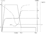
- the heating and pressing step includes a first heating and pressing step and a second heating and pressing step subsequent thereto.
- FIG. 1 shows a graph showing changes in temperature T (dashed line) and pressure P (solid line) and melt viscosity ⁇ (dotted line) of the anisotropic conductive adhesive with respect to time.
- the anisotropic conductive adhesive existing between the wiring board and the electric element is heated and flowed to a temperature equal to or higher than the temperature indicating the minimum melt viscosity ⁇ 0 (that is, the minimum melt viscosity temperature Tv).
- Tv the minimum melt viscosity temperature
- the curing rate is a numerical value defined by a decrease in characteristic absorption caused by an olefin of an acrylic compound by infrared spectroscopy.
- the pressurizing pressure P2 in the second heating and pressurizing step is set to be lower than the pressurizing pressure P1 in the first heating and pressurizing step.
- voids are efficiently removed from between the fine wiring patterns of the wiring substrate connected by the anisotropic conductive adhesive. That is, in order to extrude the void remaining between the fine wiring patterns of the wiring board from the anisotropic conductive adhesive between the wiring board and the electric element, the void is formed when the melt viscosity of the adhesive is too low. Since it becomes difficult to extrude, it is necessary to extrude the void while the melt viscosity of the adhesive is relatively high. Therefore, it is necessary to set a high pressure in the first heating and pressurizing step.
- the specific minimum melt viscosity temperature Tv of the anisotropic conductive adhesive is too low, it is difficult to form a film (film), and when it is too high, the solder may be melted. Is 70 to 150 ° C, more preferably 80 to 120 ° C.
- the specific heating temperature T1 in the first heating and pressing step is too low, the fluidity of the anisotropic conductive adhesive is lowered, and if it is too high, the solder may be melted. -160 ° C, more preferably 90-130 ° C.
- the melting temperature Ts of the solder particles is preferably 100 to 210 ° C, more preferably 130 to 170 ° C. It is.
- the heating temperature T2 in the second heating and pressurizing step is too low, the solder will not melt, and if it is too high, there is a concern that the anisotropic conductive adhesive will spring back (peel). More preferably, it is 130 to 190 ° C.
- curable acrylic compound examples include polyethylene glycol diacryl, phosphate ester acrylate, 2-hydroxyethyl acrylate, 2-hydroxypropyl acrylate, 4-hydroxybutyl acrylate, isobutyl acrylate, t-butyl acrylate, Isooctyl acrylate, bisphenoxyethanol full orange acrylate, 2-acryloyloxyethyl succinic acid, lauryl acrylate, stearyl acrylate, isobornyl acrylate, tricyclodecane dimethanol dimethacrylate, cyclohexyl acrylate, tris (2-hydroxyethyl) isocyanurate Triacrylate, tetrahydrofurfuryl acrylate, o-phthalic acid diglycidyl ether acrylate, Butoxy bisphenol A dimethacrylate, bisphenol A type epoxy acrylate, urethane acrylate, epoxy acrylate, and can be given the corresponding (meth) acrylate
- the blending amount of the curable acrylic compound in the acrylic thermosetting resin is too small, the conduction reliability tends to be low, and if it is too large, the adhesive strength tends to be low. 20 to 70% by mass, more preferably 30 to 60% by mass, based on the total amount of the system compound and the film-forming resin.
- the amount of the thermosetting initiator used in the anisotropic conductive adhesive is too small, the reactivity is lost. If the amount is too large, the cohesive force of the anisotropic conductive film tends to decrease.
- the amount is preferably 1 to 10 parts by mass, more preferably 3 to 7 parts by mass with respect to parts by mass.
- the anisotropic conductive adhesive used in the present invention is obtained by uniformly mixing and dispersing the above solder particles in an insulating acrylic thermosetting adhesive together with a solvent such as toluene, if necessary. It can be produced by molding into a film according to the method. Further, the anisotropic conductive adhesive may contain silane coupling agents, rubber components, fillers such as inorganic fillers, and various additives.
- a conventionally well-known thing can be used as a wiring board, an electrical element, and electrode which can apply the manufacturing method of this invention.
- the wiring substrate include a glass substrate, a ceramic substrate, a polyimide flexible substrate, and a silicon substrate.
- metal electrodes such as copper, aluminum, silver, and gold, metal complex oxide electrodes, such as ITO, etc. are mentioned.
- the electrode shape in this case is not particularly limited, and may be a pad shape or a bump shape.
- various electrical elements such as a bare chip, a chip size package, a semiconductor element such as an IC module, an optical element such as an LED, and a flexible wiring board can be used as the electrical element. It may be in the shape.
- anisotropic conductive adhesives A and B were prepared as described below.
- the heating and pressurizing process is not in two stages, the heating temperature is 190 ° C., and the pressure is constant at a low level (0.5 MPa), so that the indentation is insufficient. Although there was no short circuit between adjacent terminals, there was a problem in the reliability test results.
- the heating and pressurizing process is not in two stages, and the pressure is constant at a high level (3.0 MPa), and the heating temperature is 190 ° C. A short circuit occurred between adjacent terminals.
- the anisotropic conductive film B was used, and the heating temperature was lower than the melting temperature of the solder particles, and thus no metal bond was formed by the solder particles.
- Comparative Example 5 is an example in which two-step heating is performed, but since the pressure is constant and the heating temperature in the second heating and pressurizing step is 180 ° C., a short circuit due to the solder bonding of the solder particles is adjacent terminal. Occurred between.
- low temperature melting solder particles are adopted as the conductive particles constituting the anisotropic conductive adhesive, and the acrylic heat that can be cured at low temperature using the anisotropic conductive adhesive as the insulating thermosetting adhesive.
- a curable resin and also has a melting temperature of solder particles, a minimum melt viscosity temperature of an anisotropic conductive adhesive, a preheating temperature, a main heating temperature, and a preheating pressure and a main heating.
Abstract
Description
異方性導電接着剤として、溶融温度Tsのハンダ粒子が、絶縁性のアクリル系熱硬化性樹脂中に分散してなるものを使用し、異方性導電接着剤の最低溶融粘度を示す温度がTvであり、
加熱加圧工程が、第1加熱加圧工程とそれに続く第2加熱加圧工程を有し、
第1加熱加圧工程の加熱温度をT1とし、加圧圧力をP1とし、
第2加熱加圧工程の加熱温度をT2とし、加圧圧力をP2としたときに、以下の式(1)及び(2)を満足しており、
第1加熱加圧工程において、異方性導電接着剤を溶融流動させて配線基板と電気素子との間隙からプレスアウトさせ、更に予備硬化させ、
第2加熱加圧工程において、ハンダ粒子を溶融させて配線基板の電極と電気素子の電極との間に金属結合を形成させると共に異方性導電接着剤を本硬化させることを特徴とする製造方法、並びにこの製造方法により製造された接続構造体を提供する。

<加熱加圧工程>

本発明の製造方法において、異方性導電接続に使用する異方性導電接着剤としては、溶融温度Tsのハンダ粒子が最低溶融粘度温度Tvの絶縁性のアクリル系熱硬化性樹脂中に分散してペースト状あるいはフィルム状に成形されたものを使用する。
本発明の製造方法が適用できる配線基板、電気素子、電極としては、従来公知のものを使用することができる。例えば、配線基板としては、ガラス基板、セラミックス基板、ポリイミドフレキシブル基板、シリコン基板などを挙げることができる。電極としても、銅、アルミニウム、銀、金等の金属電極、ITO等の金属複合酸化物電極などが挙げられる。この場合の電極形状は、特に制限はなく、パッド状でもバンプ状でもよい。また、電気素子としては、ベアチップ、チップサイズパッケージ、ICモジュール等の半導体素子、LED等の光学素子等、フレキシブル配線板等の種々の電気素子を使用することができ、その電極もパッド状でもバンプ状でもよい。
まず、異方性導電接着剤A及びBを以下に説明するように作成した。
ビスA型フェノキシ樹脂(YP50、新日鐵化学株式会社)30質量部、液状アクリル化合物(EB3701、ダイセルサイテック株式会社)30質量部、有機過酸化物硬化剤(パーオクタ0、日油株式会社)、アクリル系シランカップリング剤(A-172、モメンティブ・パフォーマンス・マテリアルズ社)1質量部を混合し、更に平均粒子径10μmの溶融温度138℃の共晶SnBiハンダを樹脂固形分中に20質量%となるように添加し、更にトルエンを加え、固形物50wt%の異方性導電組成物を作成し、剥離処理されたPETにバーコーターを用いて塗布し、70℃のオーブンで5分乾燥させ、35μm厚の異方性導電フィルムを作製した。
異方性導電フィルムAの共晶SnBiハンダを共晶SnInハンダに変えた以外は、異方性導電フィルムAと同様に作製した。
40℃に設定された平盤上に配線板(端子導体パターン幅50μm、パターンピッチ100μm)、異方性導電フィルムA又はB、更にフレキシブル配線板(端子導体パターン幅50μm、パターンピッチ100μm)を重ね、表1の条件で加熱加圧し、接続構造体を作成した。
得られた接続構造体について、隣接間ショートの発生の有無(30V、1分間チャージ)、Jedecのレベル3相当の耐湿性(30℃、70%RH、168時間)を確保できるプレッシャークッカー(PCT(60℃、95%RH))処理時間並びに熱衝撃処理(H/S(-55℃(15分)←→125℃(15分)))サイクル数を調べた。得られた結果を表1に示す。

Claims (5)
- 配線基板の電極と電気素子の電極とが異方性導電接続されてなる接続構造体を製造する方法であって、配線基板に異方性導電接着剤を介して電気素子を載置し、その電気素子を加熱加圧することにより、配線基板の電極と電気素子の電極とを接続する加熱加圧工程を有する製造方法において、
異方性導電接着剤として、溶融温度Tsのハンダ粒子が、絶縁性のアクリル系熱硬化性樹脂中に分散してなるものを使用し、異方性導電接着剤の最低溶融粘度を示す温度がTvであり、
加熱加圧工程が、第1加熱加圧工程とそれに続く第2加熱加圧工程を有し、
第1加熱加圧工程の加熱温度をT1とし、加圧圧力をP1とし、
第2加熱加圧工程の加熱温度をT2とし、加圧圧力をP2としたときに、以下の式(1)及び(2)を満足しており、
第1加熱加圧工程において、異方性導電接着剤を溶融流動させて配線基板と電気素子との間隙からプレスアウトさせ、更に予備硬化させ、
第2加熱加圧工程において、ハンダ粒子を溶融させて配線基板の電極と電気素子の電極との間に金属結合を形成させると共に異方性導電接着剤を本硬化させることを特徴とする製造方法。 - 異方性導電接着剤の最低溶融粘度を示す温度Tvが70~150℃であり、第1加熱加圧工程の加熱温度T1が80~160℃であり、ハンダ粒子の溶融温度Tsが100~210℃であり、第2加熱加圧工程の加熱温度T2が130~220℃である請求項1記載の製造方法。
- T1とTvとの差が10~40℃であり、TsとT1との差が2~110℃であり、T2とTsとの差が2~100℃である請求項1又は2記載の製造方法。
- ハンダ粒子が、共晶SnBiハンダ粒子または共晶SnInハンダ粒子である請求項1~3のいずれかに記載の製造方法。
- 請求項1~4のいずれかに記載の製造方法により製造された接続構造体。
Priority Applications (4)
| Application Number | Priority Date | Filing Date | Title |
|---|---|---|---|
| KR1020127026255A KR101355709B1 (ko) | 2010-06-15 | 2011-06-03 | 접속 구조체의 제조 방법 및 그로부터 제조된 접속 구조체 |
| CN201180029598.1A CN102939645B (zh) | 2010-06-15 | 2011-06-03 | 连接结构体的制造方法 |
| US13/515,425 US8835772B2 (en) | 2010-06-15 | 2011-06-03 | Production method of connection structure |
| HK13105305.4A HK1178688A1 (en) | 2010-06-15 | 2013-05-02 | Process for production of connected structure |
Applications Claiming Priority (2)
| Application Number | Priority Date | Filing Date | Title |
|---|---|---|---|
| JP2010-136180 | 2010-06-15 | ||
| JP2010136180A JP5540916B2 (ja) | 2010-06-15 | 2010-06-15 | 接続構造体の製造方法 |
Publications (1)
| Publication Number | Publication Date |
|---|---|
| WO2011158666A1 true WO2011158666A1 (ja) | 2011-12-22 |
Family
ID=43042916
Family Applications (1)
| Application Number | Title | Priority Date | Filing Date |
|---|---|---|---|
| PCT/JP2011/062779 WO2011158666A1 (ja) | 2010-06-15 | 2011-06-03 | 接続構造体の製造方法 |
Country Status (7)
| Country | Link |
|---|---|
| US (1) | US8835772B2 (ja) |
| JP (1) | JP5540916B2 (ja) |
| KR (1) | KR101355709B1 (ja) |
| CN (1) | CN102939645B (ja) |
| HK (1) | HK1178688A1 (ja) |
| TW (1) | TWI480966B (ja) |
| WO (1) | WO2011158666A1 (ja) |
Cited By (3)
| Publication number | Priority date | Publication date | Assignee | Title |
|---|---|---|---|---|
| US20130161838A1 (en) * | 2011-12-23 | 2013-06-27 | Jae Sun Han | Anisotropic conductive film and semiconductor device |
| WO2015004830A1 (ja) * | 2013-07-08 | 2015-01-15 | ソニー株式会社 | 硬化条件の決定方法、回路デバイスの製造方法及び回路デバイス |
| WO2015186704A1 (ja) * | 2014-06-05 | 2015-12-10 | 積水化学工業株式会社 | 導電ペースト、接続構造体及び接続構造体の製造方法 |
Families Citing this family (38)
| Publication number | Priority date | Publication date | Assignee | Title |
|---|---|---|---|---|
| JP5673444B2 (ja) * | 2010-10-19 | 2015-02-18 | 信越化学工業株式会社 | 熱圧着用シリコーンゴムシート及び電気・電子機器部品の接合方法 |
| JP5703061B2 (ja) * | 2011-02-23 | 2015-04-15 | 積水化学工業株式会社 | 接続構造体の製造方法 |
| JP6231257B2 (ja) * | 2011-12-15 | 2017-11-15 | デクセリアルズ株式会社 | 導電性接着剤、及び電子部品の接続方法 |
| JP2014026963A (ja) * | 2012-06-18 | 2014-02-06 | Sekisui Chem Co Ltd | 接続構造体の製造方法 |
| JP2014049646A (ja) * | 2012-08-31 | 2014-03-17 | Panasonic Corp | 部品実装方法および部品実装システム |
| JP6115060B2 (ja) | 2012-09-21 | 2017-04-19 | 富士通株式会社 | 電子デバイスの製造方法 |
| JP6061645B2 (ja) * | 2012-09-24 | 2017-01-18 | 株式会社タムラ製作所 | 異方性導電性ペーストおよびそれを用いたプリント配線基板 |
| JP6068106B2 (ja) * | 2012-09-24 | 2017-01-25 | 株式会社タムラ製作所 | 異方性導電性ペーストおよびそれを用いたプリント配線基板 |
| JP6061642B2 (ja) * | 2012-09-24 | 2017-01-18 | 株式会社タムラ製作所 | 異方性導電性ペーストおよびそれを用いたプリント配線基板 |
| JP6061643B2 (ja) * | 2012-09-24 | 2017-01-18 | 株式会社タムラ製作所 | 異方性導電性ペーストおよびそれを用いたプリント配線基板 |
| JP6243111B2 (ja) * | 2012-11-14 | 2017-12-06 | 日本電産サンキョー株式会社 | 磁気センサ装置およびその製造方法 |
| JP5887304B2 (ja) * | 2013-06-21 | 2016-03-16 | 株式会社タムラ製作所 | 異方性導電性ペーストおよびそれを用いたプリント配線基板 |
| JP6393039B2 (ja) * | 2014-02-12 | 2018-09-19 | デクセリアルズ株式会社 | 接続体の製造方法、接続方法及び接続体 |
| JP6430148B2 (ja) * | 2014-05-23 | 2018-11-28 | デクセリアルズ株式会社 | 接着剤及び接続構造体 |
| US10435601B2 (en) | 2014-05-23 | 2019-10-08 | Dexerials Corporation | Adhesive agent and connection structure |
| JP6419457B2 (ja) * | 2014-05-23 | 2018-11-07 | デクセリアルズ株式会社 | 接着剤及び接続構造体 |
| KR102334672B1 (ko) * | 2014-06-03 | 2021-12-06 | 다이요 잉키 세이조 가부시키가이샤 | 경화성 조성물 및 전자 부품 |
| JP2016035044A (ja) * | 2014-06-03 | 2016-03-17 | 太陽インキ製造株式会社 | 導電性接着剤および電子部品 |
| KR20170102184A (ko) * | 2014-12-26 | 2017-09-08 | 세키스이가가쿠 고교가부시키가이샤 | 도전 페이스트, 접속 구조체 및 접속 구조체의 제조 방법 |
| JP6181038B2 (ja) * | 2014-12-26 | 2017-08-16 | 株式会社タムラ製作所 | 異方性導電性ペーストおよびそれを用いたプリント配線基板の製造方法 |
| JP2016148012A (ja) * | 2015-02-05 | 2016-08-18 | 太陽インキ製造株式会社 | 硬化性組成物および電子部品 |
| JP6705442B2 (ja) * | 2015-03-09 | 2020-06-03 | 日立化成株式会社 | 接続構造体の製造方法 |
| JP6493968B2 (ja) * | 2015-03-18 | 2019-04-03 | デクセリアルズ株式会社 | 接続方法、接合体、異方性導電フィルム、及び接合体の前駆体 |
| US10626301B2 (en) | 2015-03-18 | 2020-04-21 | Dexerials Corporation | Method for manufacturing light emitting device |
| JP6187918B2 (ja) | 2015-04-23 | 2017-08-30 | パナソニックIpマネジメント株式会社 | 回路部材の接続構造、接続方法および接続材料 |
| JP6710120B2 (ja) * | 2015-09-30 | 2020-06-17 | 太陽インキ製造株式会社 | 導電性接着剤、電子部品および電子部品の製造方法 |
| JP7321979B2 (ja) * | 2015-12-18 | 2023-08-07 | 株式会社レゾナック | 導電性接着剤組成物、接続構造体及び半導体発光素子搭載フレキシブル配線基板 |
| JP6782413B2 (ja) * | 2015-12-18 | 2020-11-11 | 昭和電工マテリアルズ株式会社 | 導電性接着剤組成物、接続構造体及び半導体発光素子搭載フレキシブル配線基板 |
| JP6587107B2 (ja) * | 2016-05-12 | 2019-10-09 | パナソニックIpマネジメント株式会社 | 回路部材の接続方法 |
| JP6772012B2 (ja) * | 2016-09-28 | 2020-10-21 | 株式会社タムラ製作所 | 異方性導電フィルムの製造方法 |
| JP6474008B2 (ja) * | 2017-03-29 | 2019-02-27 | パナソニックIpマネジメント株式会社 | 接続材料 |
| JP6536968B2 (ja) * | 2017-07-20 | 2019-07-03 | パナソニックIpマネジメント株式会社 | 接続材料 |
| JP6709944B2 (ja) * | 2018-10-01 | 2020-06-17 | 株式会社弘輝 | 接合構造体の製造方法 |
| JPWO2020085372A1 (ja) * | 2018-10-24 | 2021-09-02 | 住友ベークライト株式会社 | 導電性樹脂組成物および半導体装置 |
| JP6691998B1 (ja) * | 2019-12-24 | 2020-05-13 | 株式会社鈴木 | 半導体装置の製造方法及び半導体装置の製造装置 |
| CN111261053B (zh) * | 2020-01-20 | 2023-10-13 | 京东方科技集团股份有限公司 | 微型发光二极管显示面板及其制备方法和显示装置 |
| JP7405196B2 (ja) * | 2020-07-14 | 2023-12-26 | 株式会社レゾナック | 導電性接着剤組成物、接続構造体及び半導体発光素子搭載フレキシブル配線基板 |
| KR20240014821A (ko) * | 2022-07-26 | 2024-02-02 | 에스케이온 주식회사 | Pcb와 fpcb가 접합된 도전성 접합부를 포함하는 배터리 모듈 및 그 접합 방법 |
Citations (3)
| Publication number | Priority date | Publication date | Assignee | Title |
|---|---|---|---|---|
| JPH08325543A (ja) * | 1995-06-05 | 1996-12-10 | Soken Chem & Eng Co Ltd | 異方導電性接着剤 |
| JP2003147287A (ja) * | 2001-11-14 | 2003-05-21 | Hitachi Chem Co Ltd | 回路接続用接着フィルム |
| JP3966516B2 (ja) * | 2001-06-20 | 2007-08-29 | 東レエンジニアリング株式会社 | 実装方法および装置 |
Family Cites Families (17)
| Publication number | Priority date | Publication date | Assignee | Title |
|---|---|---|---|---|
| JP3636159B2 (ja) * | 1992-09-08 | 2005-04-06 | セイコーエプソン株式会社 | 液晶表示装置、半導体チップの実装構造、電子光学装置および電子印字装置 |
| JP3417110B2 (ja) | 1994-12-30 | 2003-06-16 | カシオ計算機株式会社 | 電子部品の接続方法 |
| US5965064A (en) * | 1997-10-28 | 1999-10-12 | Sony Chemicals Corporation | Anisotropically electroconductive adhesive and adhesive film |
| JP2001015551A (ja) * | 1999-06-29 | 2001-01-19 | Toshiba Corp | 半導体装置およびその製造方法 |
| JP4411819B2 (ja) * | 2000-03-23 | 2010-02-10 | ソニー株式会社 | 電気的接続材料 |
| JP3968516B2 (ja) * | 2002-09-10 | 2007-08-29 | 井関農機株式会社 | 農作業機 |
| US7034403B2 (en) | 2003-04-10 | 2006-04-25 | 3M Innovative Properties Company | Durable electronic assembly with conductive adhesive |
| US7754529B2 (en) * | 2005-02-03 | 2010-07-13 | Panasonic Corporation | Flip chip mounting body and method for mounting such flip chip mounting body and bump forming method |
| WO2006098268A1 (ja) * | 2005-03-16 | 2006-09-21 | Matsushita Electric Industrial Co., Ltd. | 導電性粒子を用いたフリップチップ実装方法およびバンプ形成方法 |
| KR101181140B1 (ko) * | 2005-03-29 | 2012-09-14 | 파나소닉 주식회사 | 플립칩 실장방법 및 기판간 접속방법 |
| JP5329028B2 (ja) * | 2006-09-15 | 2013-10-30 | パナソニック株式会社 | 電子部品実装構造体の製造方法 |
| KR101079946B1 (ko) * | 2006-11-28 | 2011-11-04 | 파나소닉 주식회사 | 전자 부품 실장 구조체와 그 제조 방법 |
| TW200839895A (en) * | 2007-03-16 | 2008-10-01 | Int Semiconductor Tech Ltd | Method for flip-chip bonding with non-conductive paste |
| JP5093482B2 (ja) * | 2007-06-26 | 2012-12-12 | ソニーケミカル&インフォメーションデバイス株式会社 | 異方性導電材料、接続構造体及びその製造方法 |
| JP2009141269A (ja) * | 2007-12-10 | 2009-06-25 | Sony Chemical & Information Device Corp | 電気部品の実装方法及び実装装置 |
| KR101633945B1 (ko) * | 2008-11-06 | 2016-06-27 | 스미토모 베이클리트 컴퍼니 리미티드 | 전자 장치의 제조 방법 및 전자 장치 |
| JPWO2010070779A1 (ja) * | 2008-12-19 | 2012-05-24 | パナソニック株式会社 | 異方性導電樹脂、基板接続構造及び電子機器 |
-
2010
- 2010-06-15 JP JP2010136180A patent/JP5540916B2/ja active Active
-
2011
- 2011-06-03 CN CN201180029598.1A patent/CN102939645B/zh active Active
- 2011-06-03 US US13/515,425 patent/US8835772B2/en active Active
- 2011-06-03 KR KR1020127026255A patent/KR101355709B1/ko active IP Right Grant
- 2011-06-03 WO PCT/JP2011/062779 patent/WO2011158666A1/ja active Application Filing
- 2011-06-09 TW TW100120096A patent/TWI480966B/zh active
-
2013
- 2013-05-02 HK HK13105305.4A patent/HK1178688A1/xx unknown
Patent Citations (3)
| Publication number | Priority date | Publication date | Assignee | Title |
|---|---|---|---|---|
| JPH08325543A (ja) * | 1995-06-05 | 1996-12-10 | Soken Chem & Eng Co Ltd | 異方導電性接着剤 |
| JP3966516B2 (ja) * | 2001-06-20 | 2007-08-29 | 東レエンジニアリング株式会社 | 実装方法および装置 |
| JP2003147287A (ja) * | 2001-11-14 | 2003-05-21 | Hitachi Chem Co Ltd | 回路接続用接着フィルム |
Cited By (11)
| Publication number | Priority date | Publication date | Assignee | Title |
|---|---|---|---|---|
| US20130161838A1 (en) * | 2011-12-23 | 2013-06-27 | Jae Sun Han | Anisotropic conductive film and semiconductor device |
| US9263372B2 (en) * | 2011-12-23 | 2016-02-16 | Cheil Industries, Inc. | Anisotropic conductive film and semiconductor device |
| WO2015004830A1 (ja) * | 2013-07-08 | 2015-01-15 | ソニー株式会社 | 硬化条件の決定方法、回路デバイスの製造方法及び回路デバイス |
| CN104428881A (zh) * | 2013-07-08 | 2015-03-18 | 索尼公司 | 固化条件的确定方法、电路器件的生产方法和电路器件 |
| JP5700186B1 (ja) * | 2013-07-08 | 2015-04-15 | ソニー株式会社 | 硬化条件の決定方法、回路デバイスの製造方法及び回路デバイス |
| CN104428881B (zh) * | 2013-07-08 | 2017-06-09 | 索尼公司 | 固化条件的确定方法、电路器件的生产方法和电路器件 |
| US9997491B2 (en) | 2013-07-08 | 2018-06-12 | Sony Corporation | Method of determining curing conditions, method of producing circuit device, and circuit device |
| US10658329B2 (en) | 2013-07-08 | 2020-05-19 | Sony Corporation | Method of determining curing conditions, method of producing circuit device and circuit device |
| WO2015186704A1 (ja) * | 2014-06-05 | 2015-12-10 | 積水化学工業株式会社 | 導電ペースト、接続構造体及び接続構造体の製造方法 |
| JP5860191B1 (ja) * | 2014-06-05 | 2016-02-16 | 積水化学工業株式会社 | 導電ペースト、接続構造体及び接続構造体の製造方法 |
| JP2016103481A (ja) * | 2014-06-05 | 2016-06-02 | 積水化学工業株式会社 | 導電ペースト、接続構造体及び接続構造体の製造方法 |
Also Published As
| Publication number | Publication date |
|---|---|
| US8835772B2 (en) | 2014-09-16 |
| CN102939645A (zh) | 2013-02-20 |
| HK1178688A1 (en) | 2013-09-13 |
| CN102939645B (zh) | 2015-06-10 |
| TWI480966B (zh) | 2015-04-11 |
| JP5540916B2 (ja) | 2014-07-02 |
| JP2010226140A (ja) | 2010-10-07 |
| KR101355709B1 (ko) | 2014-01-27 |
| US20120255766A1 (en) | 2012-10-11 |
| KR20120136386A (ko) | 2012-12-18 |
| TW201207972A (en) | 2012-02-16 |
Similar Documents
| Publication | Publication Date | Title |
|---|---|---|
| WO2011158666A1 (ja) | 接続構造体の製造方法 | |
| KR101098205B1 (ko) | 이방성 도전 필름 | |
| JP2010226140A5 (ja) | ||
| US20120292082A1 (en) | Anisotropic conductive film | |
| CN108702845B (zh) | 连接结构体的制造方法 | |
| TWI468487B (zh) | An anisotropic conductive material, a method for manufacturing the same, and a structure thereof and a method for manufacturing the same | |
| EP2792722B1 (en) | Method for connecting electronic components and assembly resulting therefrom | |
| KR20210134875A (ko) | 접착제 조성물 및 접속체 | |
| JP5844588B2 (ja) | 回路接続材料及びそれを用いた接続方法並びに接続構造体 | |
| JP5972564B2 (ja) | 接続方法、接続構造体、異方性導電フィルム及びその製造方法 | |
| TWI539470B (zh) | An anisotropic conductive connecting material, a film laminate, a connecting method, and a connecting structure | |
| JP2013103947A (ja) | 回路接続用接着剤フィルム並びにそれを用いた回路接続体及び回路接続体の製造方法 | |
| KR20140104013A (ko) | 접착제, 및 전자 부품의 접속 방법 |
Legal Events
| Date | Code | Title | Description |
|---|---|---|---|
| WWE | Wipo information: entry into national phase |
Ref document number: 201180029598.1 Country of ref document: CN |
|
| 121 | Ep: the epo has been informed by wipo that ep was designated in this application |
Ref document number: 11795574 Country of ref document: EP Kind code of ref document: A1 |
|
| WWE | Wipo information: entry into national phase |
Ref document number: 13515425 Country of ref document: US |
|
| ENP | Entry into the national phase |
Ref document number: 20127026255 Country of ref document: KR Kind code of ref document: A |
|
| NENP | Non-entry into the national phase |
Ref country code: DE |
|
| 122 | Ep: pct application non-entry in european phase |
Ref document number: 11795574 Country of ref document: EP Kind code of ref document: A1 |