WO2011027659A1 - ソルダペースト、それを用いた接合方法、および接合構造 - Google Patents
ソルダペースト、それを用いた接合方法、および接合構造 Download PDFInfo
- Publication number
- WO2011027659A1 WO2011027659A1 PCT/JP2010/063681 JP2010063681W WO2011027659A1 WO 2011027659 A1 WO2011027659 A1 WO 2011027659A1 JP 2010063681 W JP2010063681 W JP 2010063681W WO 2011027659 A1 WO2011027659 A1 WO 2011027659A1
- Authority
- WO
- WIPO (PCT)
- Prior art keywords
- metal
- solder paste
- alloy
- resin
- intermetallic compound
- Prior art date
- Legal status (The legal status is an assumption and is not a legal conclusion. Google has not performed a legal analysis and makes no representation as to the accuracy of the status listed.)
- Ceased
Links
Images


Classifications
-
- B—PERFORMING OPERATIONS; TRANSPORTING
- B23—MACHINE TOOLS; METAL-WORKING NOT OTHERWISE PROVIDED FOR
- B23K—SOLDERING OR UNSOLDERING; WELDING; CLADDING OR PLATING BY SOLDERING OR WELDING; CUTTING BY APPLYING HEAT LOCALLY, e.g. FLAME CUTTING; WORKING BY LASER BEAM
- B23K35/00—Rods, electrodes, materials, or media, for use in soldering, welding, or cutting
- B23K35/02—Rods, electrodes, materials, or media, for use in soldering, welding, or cutting characterised by mechanical features, e.g. shape
- B23K35/0222—Rods, electrodes, materials, or media, for use in soldering, welding, or cutting characterised by mechanical features, e.g. shape for use in soldering or brazing
- B23K35/0244—Powders, particles or spheres; Preforms made therefrom
- B23K35/025—Pastes, creams or slurries
-
- B—PERFORMING OPERATIONS; TRANSPORTING
- B23—MACHINE TOOLS; METAL-WORKING NOT OTHERWISE PROVIDED FOR
- B23K—SOLDERING OR UNSOLDERING; WELDING; CLADDING OR PLATING BY SOLDERING OR WELDING; CUTTING BY APPLYING HEAT LOCALLY, e.g. FLAME CUTTING; WORKING BY LASER BEAM
- B23K35/00—Rods, electrodes, materials, or media, for use in soldering, welding, or cutting
- B23K35/22—Rods, electrodes, materials, or media, for use in soldering, welding, or cutting characterised by the composition or nature of the material
-
- B—PERFORMING OPERATIONS; TRANSPORTING
- B23—MACHINE TOOLS; METAL-WORKING NOT OTHERWISE PROVIDED FOR
- B23K—SOLDERING OR UNSOLDERING; WELDING; CLADDING OR PLATING BY SOLDERING OR WELDING; CUTTING BY APPLYING HEAT LOCALLY, e.g. FLAME CUTTING; WORKING BY LASER BEAM
- B23K1/00—Soldering, e.g. brazing, or unsoldering
-
- B—PERFORMING OPERATIONS; TRANSPORTING
- B23—MACHINE TOOLS; METAL-WORKING NOT OTHERWISE PROVIDED FOR
- B23K—SOLDERING OR UNSOLDERING; WELDING; CLADDING OR PLATING BY SOLDERING OR WELDING; CUTTING BY APPLYING HEAT LOCALLY, e.g. FLAME CUTTING; WORKING BY LASER BEAM
- B23K1/00—Soldering, e.g. brazing, or unsoldering
- B23K1/0008—Soldering, e.g. brazing, or unsoldering specially adapted for particular articles or work
- B23K1/0016—Soldering of electronic components
-
- B—PERFORMING OPERATIONS; TRANSPORTING
- B23—MACHINE TOOLS; METAL-WORKING NOT OTHERWISE PROVIDED FOR
- B23K—SOLDERING OR UNSOLDERING; WELDING; CLADDING OR PLATING BY SOLDERING OR WELDING; CUTTING BY APPLYING HEAT LOCALLY, e.g. FLAME CUTTING; WORKING BY LASER BEAM
- B23K35/00—Rods, electrodes, materials, or media, for use in soldering, welding, or cutting
- B23K35/22—Rods, electrodes, materials, or media, for use in soldering, welding, or cutting characterised by the composition or nature of the material
- B23K35/24—Selection of soldering or welding materials proper
- B23K35/26—Selection of soldering or welding materials proper with the principal constituent melting at less than 400°C
-
- B—PERFORMING OPERATIONS; TRANSPORTING
- B23—MACHINE TOOLS; METAL-WORKING NOT OTHERWISE PROVIDED FOR
- B23K—SOLDERING OR UNSOLDERING; WELDING; CLADDING OR PLATING BY SOLDERING OR WELDING; CUTTING BY APPLYING HEAT LOCALLY, e.g. FLAME CUTTING; WORKING BY LASER BEAM
- B23K35/00—Rods, electrodes, materials, or media, for use in soldering, welding, or cutting
- B23K35/22—Rods, electrodes, materials, or media, for use in soldering, welding, or cutting characterised by the composition or nature of the material
- B23K35/24—Selection of soldering or welding materials proper
- B23K35/26—Selection of soldering or welding materials proper with the principal constituent melting at less than 400°C
- B23K35/262—Sn as the principal constituent
-
- B—PERFORMING OPERATIONS; TRANSPORTING
- B23—MACHINE TOOLS; METAL-WORKING NOT OTHERWISE PROVIDED FOR
- B23K—SOLDERING OR UNSOLDERING; WELDING; CLADDING OR PLATING BY SOLDERING OR WELDING; CUTTING BY APPLYING HEAT LOCALLY, e.g. FLAME CUTTING; WORKING BY LASER BEAM
- B23K35/00—Rods, electrodes, materials, or media, for use in soldering, welding, or cutting
- B23K35/22—Rods, electrodes, materials, or media, for use in soldering, welding, or cutting characterised by the composition or nature of the material
- B23K35/24—Selection of soldering or welding materials proper
- B23K35/30—Selection of soldering or welding materials proper with the principal constituent melting at less than 1550°C
-
- B—PERFORMING OPERATIONS; TRANSPORTING
- B23—MACHINE TOOLS; METAL-WORKING NOT OTHERWISE PROVIDED FOR
- B23K—SOLDERING OR UNSOLDERING; WELDING; CLADDING OR PLATING BY SOLDERING OR WELDING; CUTTING BY APPLYING HEAT LOCALLY, e.g. FLAME CUTTING; WORKING BY LASER BEAM
- B23K35/00—Rods, electrodes, materials, or media, for use in soldering, welding, or cutting
- B23K35/22—Rods, electrodes, materials, or media, for use in soldering, welding, or cutting characterised by the composition or nature of the material
- B23K35/36—Selection of non-metallic compositions, e.g. coatings or fluxes; Selection of soldering or welding materials, conjoint with selection of non-metallic compositions, both selections being of interest
- B23K35/3612—Selection of non-metallic compositions, e.g. coatings or fluxes; Selection of soldering or welding materials, conjoint with selection of non-metallic compositions, both selections being of interest with organic compounds as principal constituents
- B23K35/3613—Polymers, e.g. resins
-
- B—PERFORMING OPERATIONS; TRANSPORTING
- B23—MACHINE TOOLS; METAL-WORKING NOT OTHERWISE PROVIDED FOR
- B23K—SOLDERING OR UNSOLDERING; WELDING; CLADDING OR PLATING BY SOLDERING OR WELDING; CUTTING BY APPLYING HEAT LOCALLY, e.g. FLAME CUTTING; WORKING BY LASER BEAM
- B23K35/00—Rods, electrodes, materials, or media, for use in soldering, welding, or cutting
- B23K35/22—Rods, electrodes, materials, or media, for use in soldering, welding, or cutting characterised by the composition or nature of the material
- B23K35/36—Selection of non-metallic compositions, e.g. coatings or fluxes; Selection of soldering or welding materials, conjoint with selection of non-metallic compositions, both selections being of interest
- B23K35/362—Selection of compositions of fluxes
-
- C—CHEMISTRY; METALLURGY
- C22—METALLURGY; FERROUS OR NON-FERROUS ALLOYS; TREATMENT OF ALLOYS OR NON-FERROUS METALS
- C22C—ALLOYS
- C22C13/00—Alloys based on tin
-
- C—CHEMISTRY; METALLURGY
- C22—METALLURGY; FERROUS OR NON-FERROUS ALLOYS; TREATMENT OF ALLOYS OR NON-FERROUS METALS
- C22C—ALLOYS
- C22C9/00—Alloys based on copper
- C22C9/05—Alloys based on copper with manganese as the next major constituent
-
- C—CHEMISTRY; METALLURGY
- C22—METALLURGY; FERROUS OR NON-FERROUS ALLOYS; TREATMENT OF ALLOYS OR NON-FERROUS METALS
- C22C—ALLOYS
- C22C9/00—Alloys based on copper
- C22C9/06—Alloys based on copper with nickel or cobalt as the next major constituent
-
- H—ELECTRICITY
- H05—ELECTRIC TECHNIQUES NOT OTHERWISE PROVIDED FOR
- H05K—PRINTED CIRCUITS; CASINGS OR CONSTRUCTIONAL DETAILS OF ELECTRIC APPARATUS; MANUFACTURE OF ASSEMBLAGES OF ELECTRICAL COMPONENTS
- H05K3/00—Apparatus or processes for manufacturing printed circuits
- H05K3/30—Assembling printed circuits with electric components, e.g. with resistors
- H05K3/32—Assembling printed circuits with electric components, e.g. with resistors electrically connecting electric components or wires to printed circuits
- H05K3/34—Assembling printed circuits with electric components, e.g. with resistors electrically connecting electric components or wires to printed circuits by soldering
- H05K3/3465—Application of solder
- H05K3/3485—Application of solder paste, slurry or powder
-
- B—PERFORMING OPERATIONS; TRANSPORTING
- B23—MACHINE TOOLS; METAL-WORKING NOT OTHERWISE PROVIDED FOR
- B23K—SOLDERING OR UNSOLDERING; WELDING; CLADDING OR PLATING BY SOLDERING OR WELDING; CUTTING BY APPLYING HEAT LOCALLY, e.g. FLAME CUTTING; WORKING BY LASER BEAM
- B23K2101/00—Articles made by soldering, welding or cutting
- B23K2101/36—Electric or electronic devices
- B23K2101/40—Semiconductor devices
-
- H—ELECTRICITY
- H05—ELECTRIC TECHNIQUES NOT OTHERWISE PROVIDED FOR
- H05K—PRINTED CIRCUITS; CASINGS OR CONSTRUCTIONAL DETAILS OF ELECTRIC APPARATUS; MANUFACTURE OF ASSEMBLAGES OF ELECTRICAL COMPONENTS
- H05K2201/00—Indexing scheme relating to printed circuits covered by H05K1/00
- H05K2201/02—Fillers; Particles; Fibers; Reinforcement materials
- H05K2201/0203—Fillers and particles
- H05K2201/0206—Materials
- H05K2201/0215—Metallic fillers
-
- H—ELECTRICITY
- H05—ELECTRIC TECHNIQUES NOT OTHERWISE PROVIDED FOR
- H05K—PRINTED CIRCUITS; CASINGS OR CONSTRUCTIONAL DETAILS OF ELECTRIC APPARATUS; MANUFACTURE OF ASSEMBLAGES OF ELECTRICAL COMPONENTS
- H05K2201/00—Indexing scheme relating to printed circuits covered by H05K1/00
- H05K2201/02—Fillers; Particles; Fibers; Reinforcement materials
- H05K2201/0203—Fillers and particles
- H05K2201/0263—Details about a collection of particles
- H05K2201/0272—Mixed conductive particles, i.e. using different conductive particles, e.g. differing in shape
-
- H—ELECTRICITY
- H10—SEMICONDUCTOR DEVICES; ELECTRIC SOLID-STATE DEVICES NOT OTHERWISE PROVIDED FOR
- H10W—GENERIC PACKAGES, INTERCONNECTIONS, CONNECTORS OR OTHER CONSTRUCTIONAL DETAILS OF DEVICES COVERED BY CLASS H10
- H10W72/00—Interconnections or connectors in packages
- H10W72/01—Manufacture or treatment
- H10W72/012—Manufacture or treatment of bump connectors, dummy bumps or thermal bumps
- H10W72/01221—Manufacture or treatment of bump connectors, dummy bumps or thermal bumps using local deposition
- H10W72/01223—Manufacture or treatment of bump connectors, dummy bumps or thermal bumps using local deposition in liquid form, e.g. by dispensing droplets or by screen printing
-
- H—ELECTRICITY
- H10—SEMICONDUCTOR DEVICES; ELECTRIC SOLID-STATE DEVICES NOT OTHERWISE PROVIDED FOR
- H10W—GENERIC PACKAGES, INTERCONNECTIONS, CONNECTORS OR OTHER CONSTRUCTIONAL DETAILS OF DEVICES COVERED BY CLASS H10
- H10W72/00—Interconnections or connectors in packages
- H10W72/01—Manufacture or treatment
- H10W72/012—Manufacture or treatment of bump connectors, dummy bumps or thermal bumps
- H10W72/01221—Manufacture or treatment of bump connectors, dummy bumps or thermal bumps using local deposition
- H10W72/01225—Manufacture or treatment of bump connectors, dummy bumps or thermal bumps using local deposition in solid form, e.g. by using a powder or by stud bumping
-
- H—ELECTRICITY
- H10—SEMICONDUCTOR DEVICES; ELECTRIC SOLID-STATE DEVICES NOT OTHERWISE PROVIDED FOR
- H10W—GENERIC PACKAGES, INTERCONNECTIONS, CONNECTORS OR OTHER CONSTRUCTIONAL DETAILS OF DEVICES COVERED BY CLASS H10
- H10W72/00—Interconnections or connectors in packages
- H10W72/01—Manufacture or treatment
- H10W72/013—Manufacture or treatment of die-attach connectors
- H10W72/01321—Manufacture or treatment of die-attach connectors using local deposition
- H10W72/01323—Manufacture or treatment of die-attach connectors using local deposition in liquid form, e.g. by dispensing droplets or by screen printing
-
- H—ELECTRICITY
- H10—SEMICONDUCTOR DEVICES; ELECTRIC SOLID-STATE DEVICES NOT OTHERWISE PROVIDED FOR
- H10W—GENERIC PACKAGES, INTERCONNECTIONS, CONNECTORS OR OTHER CONSTRUCTIONAL DETAILS OF DEVICES COVERED BY CLASS H10
- H10W72/00—Interconnections or connectors in packages
- H10W72/071—Connecting or disconnecting
- H10W72/072—Connecting or disconnecting of bump connectors
-
- H—ELECTRICITY
- H10—SEMICONDUCTOR DEVICES; ELECTRIC SOLID-STATE DEVICES NOT OTHERWISE PROVIDED FOR
- H10W—GENERIC PACKAGES, INTERCONNECTIONS, CONNECTORS OR OTHER CONSTRUCTIONAL DETAILS OF DEVICES COVERED BY CLASS H10
- H10W72/00—Interconnections or connectors in packages
- H10W72/071—Connecting or disconnecting
- H10W72/072—Connecting or disconnecting of bump connectors
- H10W72/07231—Techniques
- H10W72/07234—Using a reflow oven
-
- H—ELECTRICITY
- H10—SEMICONDUCTOR DEVICES; ELECTRIC SOLID-STATE DEVICES NOT OTHERWISE PROVIDED FOR
- H10W—GENERIC PACKAGES, INTERCONNECTIONS, CONNECTORS OR OTHER CONSTRUCTIONAL DETAILS OF DEVICES COVERED BY CLASS H10
- H10W72/00—Interconnections or connectors in packages
- H10W72/071—Connecting or disconnecting
- H10W72/072—Connecting or disconnecting of bump connectors
- H10W72/07231—Techniques
- H10W72/07236—Soldering or alloying
-
- H—ELECTRICITY
- H10—SEMICONDUCTOR DEVICES; ELECTRIC SOLID-STATE DEVICES NOT OTHERWISE PROVIDED FOR
- H10W—GENERIC PACKAGES, INTERCONNECTIONS, CONNECTORS OR OTHER CONSTRUCTIONAL DETAILS OF DEVICES COVERED BY CLASS H10
- H10W72/00—Interconnections or connectors in packages
- H10W72/071—Connecting or disconnecting
- H10W72/072—Connecting or disconnecting of bump connectors
- H10W72/07251—Connecting or disconnecting of bump connectors characterised by changes in properties of the bump connectors during connecting
- H10W72/07255—Connecting or disconnecting of bump connectors characterised by changes in properties of the bump connectors during connecting changes in materials
-
- H—ELECTRICITY
- H10—SEMICONDUCTOR DEVICES; ELECTRIC SOLID-STATE DEVICES NOT OTHERWISE PROVIDED FOR
- H10W—GENERIC PACKAGES, INTERCONNECTIONS, CONNECTORS OR OTHER CONSTRUCTIONAL DETAILS OF DEVICES COVERED BY CLASS H10
- H10W72/00—Interconnections or connectors in packages
- H10W72/071—Connecting or disconnecting
- H10W72/073—Connecting or disconnecting of die-attach connectors
-
- H—ELECTRICITY
- H10—SEMICONDUCTOR DEVICES; ELECTRIC SOLID-STATE DEVICES NOT OTHERWISE PROVIDED FOR
- H10W—GENERIC PACKAGES, INTERCONNECTIONS, CONNECTORS OR OTHER CONSTRUCTIONAL DETAILS OF DEVICES COVERED BY CLASS H10
- H10W72/00—Interconnections or connectors in packages
- H10W72/071—Connecting or disconnecting
- H10W72/073—Connecting or disconnecting of die-attach connectors
- H10W72/07331—Connecting techniques
- H10W72/07334—Using a reflow oven
-
- H—ELECTRICITY
- H10—SEMICONDUCTOR DEVICES; ELECTRIC SOLID-STATE DEVICES NOT OTHERWISE PROVIDED FOR
- H10W—GENERIC PACKAGES, INTERCONNECTIONS, CONNECTORS OR OTHER CONSTRUCTIONAL DETAILS OF DEVICES COVERED BY CLASS H10
- H10W72/00—Interconnections or connectors in packages
- H10W72/071—Connecting or disconnecting
- H10W72/073—Connecting or disconnecting of die-attach connectors
- H10W72/07331—Connecting techniques
- H10W72/07336—Soldering or alloying
-
- H—ELECTRICITY
- H10—SEMICONDUCTOR DEVICES; ELECTRIC SOLID-STATE DEVICES NOT OTHERWISE PROVIDED FOR
- H10W—GENERIC PACKAGES, INTERCONNECTIONS, CONNECTORS OR OTHER CONSTRUCTIONAL DETAILS OF DEVICES COVERED BY CLASS H10
- H10W72/00—Interconnections or connectors in packages
- H10W72/071—Connecting or disconnecting
- H10W72/073—Connecting or disconnecting of die-attach connectors
- H10W72/07351—Connecting or disconnecting of die-attach connectors characterised by changes in properties of the die-attach connectors during connecting
- H10W72/07355—Connecting or disconnecting of die-attach connectors characterised by changes in properties of the die-attach connectors during connecting changes in materials
-
- H—ELECTRICITY
- H10—SEMICONDUCTOR DEVICES; ELECTRIC SOLID-STATE DEVICES NOT OTHERWISE PROVIDED FOR
- H10W—GENERIC PACKAGES, INTERCONNECTIONS, CONNECTORS OR OTHER CONSTRUCTIONAL DETAILS OF DEVICES COVERED BY CLASS H10
- H10W72/00—Interconnections or connectors in packages
- H10W72/20—Bump connectors, e.g. solder bumps or copper pillars; Dummy bumps; Thermal bumps
- H10W72/221—Structures or relative sizes
- H10W72/225—Bumps having a filler embedded in a matrix
-
- H—ELECTRICITY
- H10—SEMICONDUCTOR DEVICES; ELECTRIC SOLID-STATE DEVICES NOT OTHERWISE PROVIDED FOR
- H10W—GENERIC PACKAGES, INTERCONNECTIONS, CONNECTORS OR OTHER CONSTRUCTIONAL DETAILS OF DEVICES COVERED BY CLASS H10
- H10W72/00—Interconnections or connectors in packages
- H10W72/20—Bump connectors, e.g. solder bumps or copper pillars; Dummy bumps; Thermal bumps
- H10W72/241—Dispositions, e.g. layouts
-
- H—ELECTRICITY
- H10—SEMICONDUCTOR DEVICES; ELECTRIC SOLID-STATE DEVICES NOT OTHERWISE PROVIDED FOR
- H10W—GENERIC PACKAGES, INTERCONNECTIONS, CONNECTORS OR OTHER CONSTRUCTIONAL DETAILS OF DEVICES COVERED BY CLASS H10
- H10W72/00—Interconnections or connectors in packages
- H10W72/20—Bump connectors, e.g. solder bumps or copper pillars; Dummy bumps; Thermal bumps
- H10W72/251—Materials
- H10W72/252—Materials comprising solid metals or solid metalloids, e.g. PbSn, Ag or Cu
-
- H—ELECTRICITY
- H10—SEMICONDUCTOR DEVICES; ELECTRIC SOLID-STATE DEVICES NOT OTHERWISE PROVIDED FOR
- H10W—GENERIC PACKAGES, INTERCONNECTIONS, CONNECTORS OR OTHER CONSTRUCTIONAL DETAILS OF DEVICES COVERED BY CLASS H10
- H10W72/00—Interconnections or connectors in packages
- H10W72/20—Bump connectors, e.g. solder bumps or copper pillars; Dummy bumps; Thermal bumps
- H10W72/251—Materials
- H10W72/252—Materials comprising solid metals or solid metalloids, e.g. PbSn, Ag or Cu
- H10W72/2528—Intermetallic compounds
-
- H—ELECTRICITY
- H10—SEMICONDUCTOR DEVICES; ELECTRIC SOLID-STATE DEVICES NOT OTHERWISE PROVIDED FOR
- H10W—GENERIC PACKAGES, INTERCONNECTIONS, CONNECTORS OR OTHER CONSTRUCTIONAL DETAILS OF DEVICES COVERED BY CLASS H10
- H10W72/00—Interconnections or connectors in packages
- H10W72/20—Bump connectors, e.g. solder bumps or copper pillars; Dummy bumps; Thermal bumps
- H10W72/251—Materials
- H10W72/253—Materials not comprising solid metals or solid metalloids, e.g. polymers or ceramics
-
- H—ELECTRICITY
- H10—SEMICONDUCTOR DEVICES; ELECTRIC SOLID-STATE DEVICES NOT OTHERWISE PROVIDED FOR
- H10W—GENERIC PACKAGES, INTERCONNECTIONS, CONNECTORS OR OTHER CONSTRUCTIONAL DETAILS OF DEVICES COVERED BY CLASS H10
- H10W72/00—Interconnections or connectors in packages
- H10W72/20—Bump connectors, e.g. solder bumps or copper pillars; Dummy bumps; Thermal bumps
- H10W72/29—Bond pads specially adapted therefor
-
- H—ELECTRICITY
- H10—SEMICONDUCTOR DEVICES; ELECTRIC SOLID-STATE DEVICES NOT OTHERWISE PROVIDED FOR
- H10W—GENERIC PACKAGES, INTERCONNECTIONS, CONNECTORS OR OTHER CONSTRUCTIONAL DETAILS OF DEVICES COVERED BY CLASS H10
- H10W72/00—Interconnections or connectors in packages
- H10W72/30—Die-attach connectors
- H10W72/321—Structures or relative sizes of die-attach connectors
- H10W72/325—Die-attach connectors having a filler embedded in a matrix
-
- H—ELECTRICITY
- H10—SEMICONDUCTOR DEVICES; ELECTRIC SOLID-STATE DEVICES NOT OTHERWISE PROVIDED FOR
- H10W—GENERIC PACKAGES, INTERCONNECTIONS, CONNECTORS OR OTHER CONSTRUCTIONAL DETAILS OF DEVICES COVERED BY CLASS H10
- H10W72/00—Interconnections or connectors in packages
- H10W72/30—Die-attach connectors
- H10W72/351—Materials of die-attach connectors
- H10W72/352—Materials of die-attach connectors comprising metals or metalloids, e.g. solders
-
- H—ELECTRICITY
- H10—SEMICONDUCTOR DEVICES; ELECTRIC SOLID-STATE DEVICES NOT OTHERWISE PROVIDED FOR
- H10W—GENERIC PACKAGES, INTERCONNECTIONS, CONNECTORS OR OTHER CONSTRUCTIONAL DETAILS OF DEVICES COVERED BY CLASS H10
- H10W72/00—Interconnections or connectors in packages
- H10W72/30—Die-attach connectors
- H10W72/351—Materials of die-attach connectors
- H10W72/352—Materials of die-attach connectors comprising metals or metalloids, e.g. solders
- H10W72/3528—Intermetallic compounds
-
- H—ELECTRICITY
- H10—SEMICONDUCTOR DEVICES; ELECTRIC SOLID-STATE DEVICES NOT OTHERWISE PROVIDED FOR
- H10W—GENERIC PACKAGES, INTERCONNECTIONS, CONNECTORS OR OTHER CONSTRUCTIONAL DETAILS OF DEVICES COVERED BY CLASS H10
- H10W72/00—Interconnections or connectors in packages
- H10W72/30—Die-attach connectors
- H10W72/351—Materials of die-attach connectors
- H10W72/353—Materials of die-attach connectors not comprising solid metals or solid metalloids, e.g. ceramics
-
- H—ELECTRICITY
- H10—SEMICONDUCTOR DEVICES; ELECTRIC SOLID-STATE DEVICES NOT OTHERWISE PROVIDED FOR
- H10W—GENERIC PACKAGES, INTERCONNECTIONS, CONNECTORS OR OTHER CONSTRUCTIONAL DETAILS OF DEVICES COVERED BY CLASS H10
- H10W72/00—Interconnections or connectors in packages
- H10W72/30—Die-attach connectors
- H10W72/351—Materials of die-attach connectors
- H10W72/353—Materials of die-attach connectors not comprising solid metals or solid metalloids, e.g. ceramics
- H10W72/354—Materials of die-attach connectors not comprising solid metals or solid metalloids, e.g. ceramics comprising polymers
-
- H—ELECTRICITY
- H10—SEMICONDUCTOR DEVICES; ELECTRIC SOLID-STATE DEVICES NOT OTHERWISE PROVIDED FOR
- H10W—GENERIC PACKAGES, INTERCONNECTIONS, CONNECTORS OR OTHER CONSTRUCTIONAL DETAILS OF DEVICES COVERED BY CLASS H10
- H10W72/00—Interconnections or connectors in packages
- H10W72/50—Bond wires
- H10W72/59—Bond pads specially adapted therefor
-
- H—ELECTRICITY
- H10—SEMICONDUCTOR DEVICES; ELECTRIC SOLID-STATE DEVICES NOT OTHERWISE PROVIDED FOR
- H10W—GENERIC PACKAGES, INTERCONNECTIONS, CONNECTORS OR OTHER CONSTRUCTIONAL DETAILS OF DEVICES COVERED BY CLASS H10
- H10W72/00—Interconnections or connectors in packages
- H10W72/90—Bond pads, in general
- H10W72/921—Structures or relative sizes of bond pads
- H10W72/923—Bond pads having multiple stacked layers
-
- H—ELECTRICITY
- H10—SEMICONDUCTOR DEVICES; ELECTRIC SOLID-STATE DEVICES NOT OTHERWISE PROVIDED FOR
- H10W—GENERIC PACKAGES, INTERCONNECTIONS, CONNECTORS OR OTHER CONSTRUCTIONAL DETAILS OF DEVICES COVERED BY CLASS H10
- H10W72/00—Interconnections or connectors in packages
- H10W72/90—Bond pads, in general
- H10W72/951—Materials of bond pads
- H10W72/952—Materials of bond pads comprising metals or metalloids, e.g. PbSn, Ag or Cu
-
- Y—GENERAL TAGGING OF NEW TECHNOLOGICAL DEVELOPMENTS; GENERAL TAGGING OF CROSS-SECTIONAL TECHNOLOGIES SPANNING OVER SEVERAL SECTIONS OF THE IPC; TECHNICAL SUBJECTS COVERED BY FORMER USPC CROSS-REFERENCE ART COLLECTIONS [XRACs] AND DIGESTS
- Y10—TECHNICAL SUBJECTS COVERED BY FORMER USPC
- Y10T—TECHNICAL SUBJECTS COVERED BY FORMER US CLASSIFICATION
- Y10T428/00—Stock material or miscellaneous articles
- Y10T428/31504—Composite [nonstructural laminate]
- Y10T428/31678—Of metal
Definitions
- the present invention relates to a solder paste, a bonding method using the solder paste, and a bonding structure, and more particularly, to a solder paste used when, for example, an electronic component is mounted, a bonding method using the solder paste, and a bonding structure. .
- solder paste is widely used as a bonding material used for mounting electronic components.
- the high temperature solder include Pb-rich Pb-5Sn (melting point: 314 to 310 ° C.), Pb-10 Sn (melting point: 302 to 275 ° C.), etc.
- soldering at a temperature below the melting point of the high temperature solder using, for example, Sn-37Pb eutectic (183 ° C.) of a low temperature solder. Therefore, a method of temperature hierarchical connection in which connection by soldering is performed without melting the high-temperature solder used for the previous soldering has been widely applied.
- Such a temperature hierarchy connection is applied to, for example, a semiconductor device of a die-bonding type chip or a semiconductor device such as a flip chip connection, and after performing connection by soldering inside the semiconductor device, This is an important technique used when the semiconductor device itself is connected to a substrate by soldering.
- solder paste used in this application examples include (a) a second metal (or alloy) ball made of a second metal such as Cu, Al, Au, Ag, or a high melting point alloy containing them, and (b) Sn or A solder paste including a mixture of first metal balls made of In has been proposed (see Patent Document 1).
- Patent Document 1 discloses a joining method using a solder paste and a method for manufacturing an electronic device.
- a low melting point metal (for example, Sn) ball 51 and a high melting point metal (for example, Cu) ball 52 are schematically shown in FIG.
- the solder paste containing the flux 53 reacts by heating, and after soldering, as shown in FIG. 3B, a plurality of high melting point metal balls 52 have low melting points derived from the low melting point metal balls. It is connected via an intermetallic compound 54 formed between a metal and a refractory metal derived from a refractory metal ball, and an object to be joined is connected and connected (soldered) by this linking body. become.
- solder paste of Patent Document 1 an intermetallic compound of a high melting point metal (for example, Cu) and a low melting point metal (for example, Sn) is generated by heating the solder paste in the soldering process.
- a high melting point metal for example, Cu
- Sn low melting point metal
- the diffusion rate is slow, so that Sn which is a low melting point metal remains.
- the bonding strength at a high temperature is greatly reduced, and it may not be possible to use depending on the type of products to be bonded.
- Sn remaining in the soldering process may melt and flow out in the subsequent soldering process, and there is a problem that reliability is low as a high-temperature solder used for the temperature hierarchy connection.
- solder in the manufacturing process of the semiconductor device is used.
- Sn remaining in the attaching process may melt and flow out in the reflow soldering process.
- the present invention solves the above-mentioned problems, and produces an intermetallic compound having a good diffusibility between the first metal and the second metal in the soldering process and having a high melting point at a low temperature and in a short time. It is an object of the present invention to provide a solder paste having no melting point component and excellent heat resistance strength, and a bonding method and a bonding structure using the solder paste with high bonding reliability.
- the solder paste of the present invention is A solder paste comprising a metal component composed of a first metal powder, a second metal powder having a melting point higher than that of the first metal powder, and a flux component,
- the first metal is Sn or an alloy containing Sn
- the second metal forms an intermetallic compound exhibiting a melting point of 310 ° C. or higher with the first metal, and a lattice constant that is a difference between a lattice constant of the intermetallic compound and a lattice constant of the second metal component It is characterized by being a metal or alloy having a difference of 50% or more.
- the ratio of the second metal powder in the metal component is preferably 30% by volume or more.
- the first metal may be Sn alone, Cu, Ni, Ag, Au, Sb, Zn, Bi, In, Ge, Al, Co, Mn, Fe, Cr, Mg, Mn, Pd, Si, Sr.
- An alloy containing Sn and at least one selected from the group consisting of Te, P is desirable.
- the second metal is preferably a Cu—Mn alloy or a Cu—Ni alloy.
- the second metal is a Cu—Mn alloy in which the proportion of Mn in the second metal is 10 to 15% by weight, or Cu—Ni in which the proportion of Ni in the second metal is 10 to 15% by weight. It is desirable to be an alloy.
- the second metal powder preferably has a specific surface area of 0.05 m 2 ⁇ g ⁇ 1 or more.
- the first metal powder is coated around the second metal powder.
- the flux is (a) at least one selected from the group consisting of rosin, polymerized rosin, WW (water white) rosin, and hydrogenated rosin; (b) a rosin resin containing at least one derivative selected from the rosin group, (c) Group consisting of ethylene glycol monobutyl ether, diethylene glycol monoethyl ether, diethylene glycol monobutyl ether, and other solid components such as hydrogenated castor oil, thixotropic agents such as aliphatic amides, organic acids, and active agents such as amine hydrohalides It is desirable that at least one selected from the group consisting of a paste prepared by dissolving at least one selected from a solvent with a solvent.
- the flux is at least one selected from the group consisting of epoxy resin, phenol resin, polyimide resin, silicon resin or modified resin thereof, thermosetting resin group consisting of acrylic resin, or polyamide resin, polystyrene resin, polymethacrylic resin, It is desirable to include at least one selected from the group of thermoplastic resins consisting of polycarbonate resins and cellulose resins.
- the bonding method of the present invention is a method of bonding an object to be bonded using a solder paste, wherein the solder paste according to any one of claims 1 to 9 is used to heat and constitute the solder paste. All of one metal is made into an intermetallic compound with the second metal constituting the solder paste, and the object to be joined is joined.
- the bonding structure of the present invention is a bonding structure in which the objects to be bonded are bonded using the solder paste according to any one of claims 1 to 9,
- the joining part that joins the object to be joined is mainly composed of the second metal derived from the solder paste and an intermetallic compound containing the second metal and Sn, and is derived from the solder paste.
- the ratio of the first metal to the whole metal component is 30% by volume or less.
- the intermetallic compound is a Cu—Mn alloy or a Cu—Ni alloy, which is the second metal derived from the solder paste, and the first derived from the solder paste.
- Sn which is a metal, or Cu, Ni, Ag, Au, Sb, Zn, Bi, In, Ge, Al, Co, Mn, Fe, Cr, Mg, Mn, Pd, Si, Sr, Te, P It is desirable that it is an intermetallic compound formed between at least one selected from the group consisting of and an alloy containing Sn.
- the solder paste of the present invention is a solder paste including a metal component composed of a first metal powder, a second metal powder having a higher melting point, and a flux component, and includes Sn or Sn as the first metal.
- a first metal and a metal or alloy that generates an intermetallic compound having a melting point of 310 ° C. or higher and has a lattice constant difference of 50% or more from the intermetallic compound As a result, the diffusion of the first metal and the second metal progresses dramatically, the change to a higher melting point intermetallic compound is promoted, and the low melting point component does not remain. It becomes possible to do.
- the solder paste of the present invention for example, in a manufacturing process of a semiconductor device, after manufacturing a semiconductor device through a soldering process, the semiconductor device is mounted on a substrate by a reflow soldering method. Even in such a case, the soldering part in the previous soldering process has excellent heat resistance, so it does not remelt in the reflow soldering process and can be mounted with high reliability. It becomes possible.
- lattice constant difference means an absolute value of 100 times the value obtained by dividing the value obtained by subtracting the lattice constant of the second metal component from the lattice constant of the intermetallic compound by the lattice constant of the second metal component. Defined as a percentage (%). That is, this lattice constant difference indicates how much the lattice constant of the intermetallic compound newly generated at the interface with the second metal is different from the lattice constant of the second metal. It does not matter whether the lattice constant is large.
- FIG. 1 is a diagram schematically showing the behavior when joining is performed using the solder paste of the present invention.
- solder paste 10 is placed between the pair of electrodes 11a and 11b. Position.
- the joint is heated in this state, and when the temperature of the solder paste 10 reaches or exceeds the melting point of the first metal (Sn or Sn-containing alloy) 1 as shown in FIG.
- the first metal 1 inside melts.
- the first metal 1 when further heating is performed, the first metal 1 generates an intermetallic compound 3 (FIG. 1 (c)) with the second metal 2.
- the lattice constant difference between the intermetallic compound 3 generated at the interface between the first metal 1 and the second metal 2 and the second metal 2 is large (that is, the first metal 1).
- the difference in the lattice constant between the two metals 2 and the intermetallic compound 3 is 50% or more), so that the reaction is repeated while the intermetallic compound is peeled and dispersed in the molten first metal, and the intermetallic compound is generated.
- the content of the first metal 1 (FIGS. 1 (a) and (b)) can be sufficiently reduced within a short time after progressing dramatically.
- the first metal 1 can all be an intermetallic compound (FIG. 1 ( c)).
- the ratio of the second metal in the metal component composed of the first metal and the second metal is 30% by volume or more, the remaining ratio of Sn in the soldering process is further reduced, and the heat resistance is improved. Can be increased.
- the first metal Sn alone, Cu, Ni, Ag, Au, Sb, Zn, Bi, In, Ge, Al, Co, Mn, Fe, Cr, Mg, Mn, Pd, Si, Sr, By using an alloy containing Sn and at least one selected from the group consisting of Te and P, it becomes possible to easily form an intermetallic compound with another metal (second metal).
- the present invention can be made more effective.
- the Cu—Mn alloy having a Mn ratio of 10 to 15% by weight, or the Ni ratio being 10 to 15% by weight.
- % Cu—Ni alloy makes it easier to form intermetallic compounds with the first metal at a lower temperature and in a shorter time, and prevents melting in the subsequent reflow process. Is possible.
- the second metal may contain impurities at a ratio of 1% by weight or less, for example, to the extent that the reaction with the first metal is not hindered.
- the oxygen concentration in the first and second metal powders is preferably 2000 ppm or less, particularly preferably 10 to 1000 ppm.
- the second metal having a specific surface area of 0.05 m 2 ⁇ g ⁇ 1 or more, the probability of contact with the first metal is increased, and an intermetallic compound is further formed between the first metal and the second metal. Therefore, the high melting point can be completed with a general reflow profile.
- the present invention can be more effectively realized.
- solder paste of the present invention various known materials composed of a vehicle, a solvent, a thixotropic agent, an activator and the like can be used as a flux.
- vehicle include rosin-based resins, synthetic resins, and mixtures thereof composed of rosin and derivatives such as modified rosin modified with rosin.
- rosin resin composed of the rosin and a derivative such as a modified rosin modified from the rosin include gum rosin, tall rosin, wood rosin, polymerized rosin, hydrogenated rosin, formylated rosin, rosin ester, rosin modified malein.
- Examples include acid resins, rosin-modified phenol resins, rosin-modified alkyd resins, and other various rosin derivatives.
- Specific examples of the synthetic resin made of a rosin and a derivative such as a modified rosin obtained by modifying the rosin include a polyester resin, a polyamide resin, a phenoxy resin, and a terpene resin.
- the solvent examples include alcohols, ketones, esters, ethers, aromatics, hydrocarbons, and the like. Specific examples include benzyl alcohol, ethanol, isopropyl alcohol, butanol, diethylene glycol, ethylene glycol. , Ethyl cellosolve, butyl cellosolve, ethyl acetate, butyl acetate, butyl benzoate, diethyl adipate, dodecane, tetradecene, ⁇ -terpineol, terpineol, 2-methyl 2,4-pentanediol, 2-ethylhexanediol, toluene, xylene, Propylene glycol monophenyl ether, diethylene glycol monohexyl ether, ethylene glycol monobutyl ether, diethylene glycol monobutyl ether, diisobutyl adipate, hex Glycol, cyclohexanedim
- the thixotropic agent examples include hydrogenated castor oil, carnauba wax, amides, hydroxy fatty acids, dibenzylidene sorbitol, bis (p-methylbenzylidene) sorbitol, beeswax, stearamide, hydroxystearic acid Examples thereof include ethylene bisamide.
- fatty acids such as caprylic acid, lauric acid, myristic acid, palmitic acid, stearic acid, behenic acid, hydroxy fatty acids such as 1,2-hydroxystearic acid, antioxidants, surfactants Those added with amines can also be used as the thixotropic agent.
- Examples of the activator include amine hydrohalides, organic halogen compounds, organic acids, organic amines, polyhydric alcohols, and the like.
- Specific examples of the amine hydrohalides include diphenylguanidine. Hydrobromide, diphenylguanidine hydrochloride, cyclohexylamine hydrobromide, ethylamine hydrochloride, ethylamine hydrobromide, diethylaniline hydrobromide, diethylaniline hydrochloride, triethanolamine hydrobromic acid Examples thereof include salts and monoethanolamine hydrobromide.
- organic halogen compound examples include chlorinated paraffin, tetrabromoethane, dibromopropanol, 2,3-dibromo-1,4-butanediol, 2,3-dibromo-2-butene-1,4- Examples thereof include diol and tris (2,3-dibromopropyl) isocyanurate.
- organic acid include malonic acid, fumaric acid, glycolic acid, citric acid, malic acid, succinic acid, phenyl succinic acid, maleic acid, salicylic acid, anthranilic acid, glutaric acid, suberic acid, and adipine.
- Acid sebacic acid, stearic acid, abietic acid, benzoic acid, trimellitic acid, pyromellitic acid, dodecanoic acid, etc.
- specific organic amines include monoethanolamine, diethanolamine, triethanolamine, tributylamine Aniline, diethylaniline and the like.
- Examples of the polyhydric alcohol include erythritol, pyrogallol, and ribitol.
- solder paste of the present invention including other known ones, in particular, (a) at least one selected from the group consisting of rosin, polymerized rosin, WW (water white) rosin, hydrogenated rosin, (b) Solid components such as rosin resins containing at least one derivative selected from the rosin group, (c) thixotropic agents such as hydrogenated castor oil, aliphatic amides, activators such as organic acids and amine hydrohalides When at least one selected from the group consisting of ethylene glycol monobutyl ether, diethylene glycol monoethyl ether, diethylene glycol monobutyl ether and at least one selected from the group consisting of pastes dissolved in a solvent is used.
- the effects of the present invention can be reliably achieved.
- thermosetting resins consisting of epoxy resin, phenol resin, polyimide resin, silicon resin or modified resin thereof, acrylic resin, or polyamide resin, polystyrene resin, polymethacrylic resin, polycarbonate
- a resin containing at least one selected from the group consisting of a resin and a cellulose-based resin is used, the above-described effects of the present invention can be achieved more reliably.
- the bonding method of the present invention uses the solder paste of the present invention, and heats the low melting point metal constituting the solder paste as an intermetallic compound with the second metal constituting the solder paste. Since it is made to join, the diffusion of the first metal and the second metal in the soldering process progresses dramatically, and the change to a higher melting point intermetallic compound is promoted, and the metal component of the first metal component It becomes possible to perform soldering with a large heat resistance strength by setting the ratio to the whole to be, for example, 30% by volume or less. Furthermore, by optimizing the metal compounding ratio in the solder paste and the like, it is possible to perform a design in which the first metal component does not remain completely.
- the solder paste of the present invention for example, in a manufacturing process of a semiconductor device, after manufacturing a semiconductor device through a soldering process, the semiconductor device is mounted on a substrate by a reflow soldering method. Even in such a case, the soldering part in the previous soldering process has excellent heat resistance, so it does not remelt in the reflow soldering process and can be mounted with high reliability. It becomes possible.
- the joint part joining the objects to be joined is mainly composed of the second metal derived from the solder paste, and the intermetallic compound containing the second metal and Sn, Since the ratio with respect to the whole metal component of the 1st metal originating in a solder paste is 30 volume% or less, it becomes possible to provide a joining structure with large heat resistance strength.
- the first metal derived from the solder paste in the joint is more preferably 3% by volume or less.
- the joining structure of the present invention as shown in FIG. 1 (c), all of the first metal in the joining portion (solder) 4 joining the objects to be joined (electrodes) 11a and 11b is the first.
- the joint 4 is composed of the second metal 2 and the intermetallic compound 3, and the first metal 1 (FIGS. 1A and 1B) remains. Therefore, it is possible to realize a joint structure with high heat resistance.
- the intermetallic compound is a Cu—Mn alloy or Cu—Mn alloy that is a second metal derived from a solder paste, and a Sn simple substance that is a first metal derived from a solder paste, or Cu, Ni, At least one selected from the group consisting of Ag, Au, Sb, Zn, Bi, In, Ge, Al, Co, Mn, Fe, Cr, Mg, Mn, Pd, Si, Sr, Te, and P; and Sn
- the first metal component hardly remains and a bonded structure with high heat resistance can be provided more reliably.
- Example 1 a solder paste was prepared by mixing the first metal powder, the second metal powder, and the flux.
- the mixing ratio of the first metal powder and the second metal powder was adjusted so that the volume ratio of the first metal powder / second metal powder was 60/40 (that is, the second metal was 40% by volume).
- the first metal powder As shown in Table 1, as the first metal powder, Sn-3Ag-0.5Cu, Sn, Sn-3.5Ag, Sn-0.75Cu, Sn-58Bi, Sn-0.7Cu-0.05Ni, Sn-5Sb, Sn-2Ag-0.5Cu-2Bi, Sn-57Bi-1Ag, Sn-3.5Ag-0.5Bi-8In, Sn-9Zn, Sn-8Zn-3Bi were used.
- the average particle diameter of the first metal powder was 25 ⁇ m.
- the number 3.5 of “Sn-3.5Ag” represents the value by weight of the component (in this case, Ag), and the other materials described above and The same applies to the following description.
- the second metal powder Cu-10Ni, Cu-10Mn, Cu-12Mn-4Ni, Cu-10Mn-1P, Cu-10Ni and Cu-10Mn mixed powder, Cu Cu-10Zn was used.
- the average particle size of the second metal powder was 15 ⁇ m.
- rosin 74% by weight
- diethylene glycol monobutyl ether 22% by weight
- triethanolamine 2% by weight
- hydrogenated castor oil 2% by weight
- the produced solder paste was printed on an oxygen-free Cu plate having a size of 10 mm ⁇ 10 mm and a thickness of 0.2 mm using a metal mask.
- the metal mask had an opening diameter of 1.5 mm ⁇ 1.5 mm and a thickness of 100 ⁇ m.
- Table 1 shows the composition of the first metal and the second metal, the lattice constant of the second metal, the blending ratio of the first metal and the second metal, the type of the intermetallic compound initially formed on the surface of the second metal powder, and its The lattice constant, the difference in lattice constant between the second metal (Cu alloy) and the intermetallic compound, and the bonding strength of each bonded body (room temperature, 260 ° C.) are shown. The lattice constant is evaluated based on the a axis.
- ⁇ Residual component evaluation About 7 mg of the obtained reaction product was cut out, and differential scanning calorimetry (DSC measurement) was performed under the conditions of a measurement temperature of 30 ° C. to 300 ° C., a heating rate of 5 ° C./min, an N 2 atmosphere, and a reference Al 2 O 3 . . The amount of the first metal component remaining was quantified from the endothermic amount of the melting endothermic peak at the melting temperature of the first metal component of the obtained DSC chart. From this, the ratio of the 1st metal component with respect to the whole metal component was evaluated as a residual 1st metal component rate. A case where the residual first metal component ratio was 0 to 3% by volume was evaluated as ⁇ (excellent), and a case where it was larger than 30% by volume was evaluated as ⁇ (impossible). Table 1 also shows the residual first metal component ratio and the determination result.
- solder flow out ⁇ The solder paste is applied to a Cu land (Cu land size: 0.7 mm ⁇ 0.4 mm) of the printed circuit board (thickness: 100 ⁇ m), and the obtained applied portion has a length of 1 mm, a width of 0.5 mm, and a thickness of 0. A 5 mm chip ceramic capacitor was mounted. After reflow soldering at a peak temperature of 250 ° C, the printed circuit board is sealed with an epoxy resin and left in an environment with a relative humidity of 85%. The defect rate was evaluated. The case where the solder flow-out defect rate was 0 to 10% was evaluated as ⁇ (excellent), and the case where it was larger than 50% was evaluated as ⁇ (impossible). Table 1 also shows the solder flow failure occurrence rate and the determination result.
- the bonding strength at room temperature was 20 Nmm ⁇ 2 or more in both Examples and Comparative Examples, and it was confirmed that the bonding strength at the room temperature was practical.
- the bonding strength at 260 ° C. in the comparative example, the bonding strength was 2 Nmm ⁇ 2 or less, which was insufficient, while the example maintained 10 Nmm ⁇ 2 or more and had practical strength. was confirmed.
- the comparative example was larger than 30% by volume, whereas all the examples were 0% by volume, and the solder flow-out failure rate was 70% or more in the comparative example. On the other hand, all the examples were 0%, and it was confirmed to have high heat resistance. Moreover, in the sample of an Example, if the 1st metal was a solder alloy based on Sn, it was confirmed that it has the same high heat resistance irrespective of the kind of 1st metal.
- the second metal is a metal based on Cu—Mn (such as Cu-12Mn-4Ni and Cu-10Mn-1P), or two or more kinds of second metal powders (Cu -Mn and Cu-Ni mixed powder) were confirmed to have high heat resistance as well.
- Cu—Mn such as Cu-12Mn-4Ni and Cu-10Mn-1P
- two or more kinds of second metal powders Cu -Mn and Cu-Ni mixed powder
- the samples of the examples have high heat resistance.
- the intermetallic compound is Cu 2. MnSn and Cu 2 NiSn, which are considered to be due to the difference in lattice constant between each intermetallic compound and the second metal (Cu alloy) being 50% or more. That is, if the difference in the lattice constant between the generated intermetallic compound layer and the second metal as the base metal is large, the intermetallic compound repeats the reaction while peeling and dispersing in the molten first metal, so that the intermetallic compound is formed. This is thought to be due to the dramatic progress.
- the intermetallic compound at the bonding interface is Cu 3 Sn, and the lattice between the intermetallic compound and the second metal (Cu alloy). Since the constant difference is as small as 20% and the intermetallic compound formation does not proceed efficiently, it is considered that high heat resistance cannot be obtained.
- Sn-3Ag-0.5Cu powder was prepared as the first metal powder.
- the average particle size of the first metal powder was 25 ⁇ m.
- Cu and Cu-10Mn powders were prepared as the second metal powder.
- the average particle size of the second metal powder was 15 ⁇ m.
- As the flux rosin: 74% by weight, diethylene glycol monobutyl ether: 22% by weight, triethanolamine: 2% by weight, and hydrogenated castor oil 2% by weight were prepared.
- solder paste was produced by mixing the said 1st metal powder, the 2nd metal powder, and a flux.
- the mixing ratio was adjusted so that the volume ratio of the first metal powder / second metal powder was 87/13 to 57/43 (that is, the second metal powder was 13 to 43% by volume). Further, the blending ratio of the flux was such that the ratio of the flux in the entire solder paste was 10% by weight.
- ⁇ excellent in the case of 0 to 3% by volume, ⁇ (possible) when it exceeds 3% by volume and 30% by volume or less, and ⁇ (not possible) when it is larger than 30% by volume. ).
- solder flow-out failure rate was evaluated as ⁇ (excellent) when 0 to 10%, over 100%, ⁇ (possible) when 50% or less, and x (impossible) when larger than 50%.
- Table 2 shows the bonding strength (room temperature, 260 ° C.), residual first metal component ratio, solder flow-out failure rate, and evaluation results of each bonded body.
- the bonding strength at room temperature was 20 Nmm ⁇ 2 or more in both Examples and Comparative Examples, and it was found that practical strength was provided.
- looking at the bonding strength in the 260 ° C., and 0.1Nmm -2 in the comparative example, and far below 2Nmm -2 whereas the bonding strength is insufficient, in the embodiment 7 ⁇ 26Nmm - 2 and 2 Nmm ⁇ 2 or more were maintained, and it was confirmed that they had practical strength.
- the second metal is Cu-10Mn
- the ratio when the ratio is 30% or more, it shows a bonding strength of 23 Nmm -2 or more, and it is confirmed to have a high heat resistance strength.
- the residual first metal component ratio was larger than 30% by volume in the comparative example, but was 30% by volume or less in all the examples, and the ratio of Cu-10Mn or Cu-10Ni as the second metal.
- the residual first metal component ratio was 0% by volume in the case where the ratio was 30 volume% or more.
- the solder flow-out defective rate was 70% or more in the comparative example, but 50% or less in all the examples, and the ratio of the Cu-10Mn or Cu-10Ni as the second metal was 30%. In the above case, the solder flow-out failure rate was 0%, and it was confirmed that high heat resistance was obtained.
- Sn-3Ag-0.5Cu powder was prepared as the first metal powder.
- the average particle size of the first metal powder was 25 ⁇ m.
- a Cu—Mn alloy powder having a Mn ratio of 5 to 30 wt% and a Cu—Ni alloy powder having a Ni ratio of 5 to 20 wt% were prepared as the second metal powder.
- the average particle size of the second metal powder was 15 ⁇ m.
- As the flux rosin: 74% by weight, diethylene glycol monobutyl ether: 22% by weight, triethanolamine: 2% by weight, and hydrogenated castor oil 2% by weight were prepared.
- solder paste was produced by mixing the said 1st metal powder, the 2nd metal powder, and a flux. Further, the blending ratio of the flux was such that the ratio of the flux in the entire solder paste was 10% by weight.
- the blending ratio of the first metal powder and the second metal powder was adjusted so that the volume ratio of the first metal powder / second metal powder was 60/40 (that is, the second metal powder was 40% by volume).
- Example 2 With respect to the solder paste thus produced, in the same manner as in Example 1, the bonding strength, the residual first metal component rate, and the solder flow-out failure occurrence rate were measured, and the characteristics were evaluated. In addition, in the evaluation of the joint strength, the evaluation of the residual first metal component rate, and the solder flow-out failure rate, evaluation was performed based on the same criteria as in Example 2. Table 3 shows the bonding strength (room temperature, 260 ° C.), the residual first metal component ratio, the solder flow-out failure rate, and the evaluation results of each bonded body.
- the bonding strength at room temperature was 20 Nmm ⁇ 2 or more in both Examples and Comparative Examples, and it was found that practical strength was provided.
- looking at the bonding strength in the 260 ° C., and 0.1Nmm -2 in the comparative example, and far below 2Nmm -2 whereas the bonding strength is insufficient, in the embodiment 5 ⁇ 26Nmm - 2 and 2 Nmm ⁇ 2 or more were maintained, and it was confirmed that they had practical strength.
- the second metal is Cu-10 to 15Mn and when the second metal is Cu-10 to 15Ni, a high bonding strength of 24 to 26 Nmm ⁇ 2 is shown, and it is confirmed that the heat resistance is excellent.
- the residual first metal component ratio was larger than 30% by volume in the comparative example, whereas all the examples were 30% by volume or less, and in the case of Cu-10 to 15Mn as the second metal, and In the case of Cu-10 to 15Ni, the residual first metal component ratio was 0% by volume. Also, the solder flow-out failure rate was 70% or more in the comparative example, but 50% or less in all of the examples. Further, in the case of Cu-10 to 15Mn as the second metal, and Cu-10 In the case of ⁇ 15Ni, the solder flow-out defect rate was 0%, and it was confirmed that high heat resistance was obtained.
- Sn-3Ag-0.5Cu powder was prepared as the first metal powder.
- the average particle size of the first metal powder was 25 ⁇ m.
- Cu, Cu-10Mn alloy powder was prepared as the second metal powder.
- the average particle size of the second metal powder was 15 ⁇ m.
- the particle size of the second metal powder was changed so that the specific surface area was 0.03 to 0.06 m 2 ⁇ g ⁇ 1 .
- a rosin 74% by weight
- diethylene glycol monobutyl ether 22% by weight
- triethanolamine 2% by weight
- hydrogenated castor oil 2% by weight
- solder paste was produced by mixing the said 1st metal powder, the 2nd metal powder, and a flux. Further, the blending ratio of the flux was such that the ratio of the flux in the entire solder paste was 10% by weight.
- the blend ratio of the first metal powder and the second metal powder was adjusted so that the volume ratio of the first metal powder / second metal powder was 60/40 (that is, the second metal powder was 40% by volume).
- Example 4 shows the bonding strength (room temperature, 260 ° C.), the residual first metal component ratio, the solder flow-out failure rate, and the evaluation results of each bonded body.
- the bonding strength at room temperature was 20 Nmm ⁇ 2 or more in both Examples and Comparative Examples, and it was found that practical strength was provided.
- looking at the bonding strength in the 260 ° C., and 0.1Nmm -2 in the comparative example, and far below 2Nmm -2 whereas the bonding strength is insufficient, in the embodiment 14 ⁇ 24Nmm - 2 and 2 Nmm ⁇ 2 or more were maintained, and it was confirmed that they had practical strength.
- the specific surface area of the second metal, Cu-10Mn was 0.05 m 2 ⁇ g ⁇ 1 or more, it showed 21 Nmm ⁇ 2 or more, and had particularly high heat resistance.
- the residual first metal component ratio was larger than 30% by volume in the comparative example, whereas it was 30% by volume or less in all the examples, and the specific surface area of Cu-10Mn as the second metal was 0.00. In the case of 05 m 2 ⁇ g ⁇ 1 or more, the residual first metal component ratio was 0% by volume.
- the solder flow-out defect rate was 70% or more in the comparative example, but 50% or less in all the examples. Further, the specific surface area of the second metal Cu-10Mn was 0.05 m 2 ⁇ g. In the case of -1 or more, the solder flow-out failure rate was 0%, and it was confirmed that high heat resistance was obtained.
- solder paste was prepared by mixing a metal powder consisting of and flux.
- the mixing ratio of the first metal powder and the second metal powder is such that the volume ratio of the first metal powder / second metal powder is 60/40 (ie, the second metal powder).
- the metal powder was adjusted to 40% by volume.
- the total ratio of the Cu—Mn alloy (second metal) was 80%.
- the flux used was a blending ratio of rosin: 74% by weight, diethylene glycol monobutyl ether: 22% by weight, triethanolamine: 2% by weight, and hydrogenated castor oil 2% by weight. Further, the blending ratio of the flux was such that the ratio of the flux in the entire solder paste was 10% by weight.
- Example 2 With respect to the solder paste thus produced, in the same manner as in Example 1, the bonding strength, the residual first metal component rate, and the solder flow-out failure occurrence rate were measured, and the characteristics were evaluated. In addition, in evaluation of joining strength, a residual 1st metal component rate, and evaluation of a solder flow-out defect rate, it evaluated on the basis similar to the case of the above-mentioned Example 2. Table 5 shows the bonding strength (room temperature, 260 ° C.), the residual first metal component ratio, the solder flow-out failure rate, and the evaluation results of each bonded body.
- the bonding strength at room temperature was 20 Nmm ⁇ 2 or more in both the examples and the comparative examples, indicating that it had practical strength.
- looking at the bonding strength in the 260 ° C., and 0.1Nmm -2 in the comparative example, and far below 2Nmm -2 whereas the bonding strength is insufficient, in the embodiment 24 ⁇ 26Nmm - 2 and 2 Nmm ⁇ 2 or more were maintained, and it was confirmed that they had practical strength. From this, it was confirmed that even when the first metal is plated (coated) on the surface of the second metal, high heat resistance strength can be obtained as in the case of each of the above examples.
- the comparative examples were larger than 30% by volume, whereas the examples were all 0% by volume. Also, the solder flow-out defect rate was 70% or more in the comparative example, but 0% in the examples. Even when the first metal is plated (coated) on the surface of the second metal. It was confirmed that high heat resistance was obtained.
- Sn-3Ag-0.5Cu powder was prepared as the first metal powder.
- the average particle size of the first metal powder was 25 ⁇ m.
- a Cu-10Mn alloy powder was prepared as the second metal powder.
- the average particle size of the second metal powder was 15 ⁇ m.
- As the flux one with added resin and one without added resin were prepared.
- a general flux A having a blending ratio of rosin: 74% by weight, diethylene glycol monobutyl ether: 22% by weight, triethanolamine: 2% by weight, and hydrogenated castor oil 2% by weight is used. Prepared.
- thermosetting resin compounding flux B which added the thermosetting resin and the hardening
- An added thermoplastic resin-mixed flux C was prepared.
- thermosetting resin-mixed flux B contains the flux A, the thermosetting resin (bisphenol A type epoxy resin), and the curing agent in the following ratio.
- Flux A 30% by weight
- Thermosetting resin 40% by weight
- Curing agent 30% by weight
- thermoplastic resin-mixed flux C contains the flux A and the thermoplastic resin (polyamide resin) in the following ratio.
- Flux A 30% by weight
- Thermoplastic resin (polyamide resin) 70% by weight
- solder paste in which the above-mentioned flux A to which no resin is added is blended in such a proportion that the proportion of the flux in the entire solder paste is 10% by weight; (2) a solder paste in which the thermosetting resin blended flux B is blended in such a ratio that the proportion of the flux in the entire solder paste is 25% by weight; (3) A solder paste was prepared by blending the thermoplastic resin blended flux C in such a proportion that the proportion of the flux in the entire solder paste was 25% by weight.
- the bonding strength at room temperature was 20 Nmm ⁇ 2 or more in both Examples and Comparative Examples, and it was found that practical strength was provided.
- looking at the bonding strength in the 260 ° C., and 0.1Nmm -2 in the comparative example has significantly below 2Nmm -2, whereas the bonding strength is insufficient, in the embodiment 24 ⁇ 33Nmm - 2 and 2 Nmm ⁇ 2 or more were maintained, and it was confirmed that they had practical strength.
- the comparative examples were larger than 30% by volume, whereas the examples were all 0% by volume.
- the solder flow-out defective rate was 70% or more in the comparative example, but 0% in all the examples. It was confirmed that high heat resistance was obtained even when the resin was added.
- the lattice constant of the intermetallic compound is larger than the lattice constant of the second metal
- the lattice constant of the second metal is theoretically It can also be configured to be larger than the lattice constant of the intermetallic compound.
- the lattice constant difference 50% or more the diffusion of the first metal and the second metal progresses dramatically, and the change to the higher melting point intermetallic compound is promoted. Since one metal component hardly remains, it is possible to perform soldering with high heat resistance.
- the present invention is not limited to the above-described embodiments, and the types and compositions of the first metal and the second metal constituting the solder paste, the blending ratio of the first metal and the second metal, the components of the flux and the blend of the flux Various applications and modifications can be made within the scope of the invention with respect to the ratio and the like.
Landscapes
- Engineering & Computer Science (AREA)
- Mechanical Engineering (AREA)
- Chemical & Material Sciences (AREA)
- Materials Engineering (AREA)
- Metallurgy (AREA)
- Organic Chemistry (AREA)
- Manufacturing & Machinery (AREA)
- Microelectronics & Electronic Packaging (AREA)
- Electric Connection Of Electric Components To Printed Circuits (AREA)
Abstract
Description
ところで、従来から広く用いられてきたSn-Pb系はんだにおいては、高温系はんだとして、例えばPbリッチのPb-5Sn(融点:314~310℃)、Pb-10Sn(融点:302~275℃)などを用いて330~350℃の温度ではんだ付けし、その後、例えば、低温系はんだのSn-37Pb共晶(183℃)などを用いて、上記の高温系はんだの融点以下の温度ではんだ付けすることにより、先のはんだ付けに用いた高温系はんだを溶融させることなく、はんだ付けによる接続を行う温度階層接続の方法が広く適用されている。
また、この特許文献1には、はんだペーストを用いた接合方法や、電子機器の製造方法が開示されている。
第1金属粉末と、前記第1金属粉末よりも融点の高い第2金属粉末とからなる金属成分と、フラックス成分とを含むソルダペーストであって、
前記第1金属はSnまたはSnを含む合金であり、
前記第2金属は前記第1金属と、310℃以上の融点を示す金属間化合物を生成し、かつ、前記金属間化合物の格子定数と前記第2金属成分の格子定数との差である格子定数差が50%以上である金属または合金であること
を特徴としている。
(a)ロジン、重合ロジン、WW(water white)ロジン、水添ロジンからなるロジン群より選ばれる少なくとも1種、
(b)前記ロジン群より選ばれる少なくとも1種の誘導体を含むロジン系樹脂、
(c)硬化ヒマシ油、脂肪族アミド等のチキソ剤、有機酸、アミンのハロゲン化水素酸塩等の活性剤等の固体成分をエチレングリコールモノブチルエーテル、ジエチレングリコールモノエチルエーテル、ジエチレングリコールモノブチルエーテルからなる群より選ばれる少なくとも1種を溶剤で溶解してペースト状にしたもの
からなる群より選ばれる少なくとも1種を含むものであることが望ましい。
接合対象物を接合させている接合部は、前記ソルダペーストに由来する前記第2金属と、前記第2金属とSnとを含む金属間化合物とを主たる成分としており、前記ソルダペーストに由来する前記第1金属の金属成分全体に対する割合が30体積%以下であること
を特徴としている。
すなわち、この格子定数差は、第2金属との界面に新たに生成する金属間化合物の格子定数が、第2金属の格子定数に対してどれだけ差があるかを示すものであり、いずれの格子定数が大きいかを問わないものである。
なお、計算式で表すと以下のようになる。
格子定数差(%)={(金属間化合物の格子定数-第2金属の格子定数)/第2金属の格子定数}×100
第2金属には、第1金属との反応を阻害しない程度で、例えば、1重量%以下の割合で不純物が含まれていてもよい。不純物としては、Zn、Ge、Ti、Sn、Al、Be、Sb、In、Ga、Si、Ag、Mg、La、P、Pr、Th、Zr、B、Pd、Pt、Ni、Auなどが挙げられる。
また、接合性や反応性を考慮すると、第1および第2金属粉末中の酸素濃度は2000ppm以下であることが好ましく、特に10~1000ppmが好ましい。
前記ビヒクルの具体的な例としては、ロジンおよびそれを変性した変性ロジンなどの誘導体からなるロジン系樹脂、合成樹脂、またはこれらの混合体などが挙げられる。
また、前記ロジンおよびそれを変性した変性ロジンなどの誘導体からなるロジン系樹脂の具体的な例としては、ガムロジン、トールロジン、ウッドロジン、重合ロジン、水素添加ロジン、ホルミル化ロジン、ロジンエステル、ロジン変性マレイン酸樹脂、ロジン変性フェノール樹脂、ロジン変性アルキド樹脂、その他各種ロジン誘導体などが挙げられる。
また、ロジンおよびそれを変性した変性ロジンなどの誘導体からなる合成樹脂の具体的な例としては、ポリエステル樹脂、ポリアミド樹脂、フェノキシ樹脂、テルペン樹脂などが挙げられる。
また、前記有機酸の具体的な例として、マロン酸、フマル酸、グリコール酸、クエン酸、リンゴ酸、コハク酸、フェニルコハク酸、マレイン酸、サルチル酸、アントラニル酸、グルタル酸、スベリン酸、アジピン酸、セバシン酸、ステアリン酸、アビエチン酸、安息香酸、トリメリット酸、ピロメリット酸、ドデカン酸などがあり、さらに有機アミンの具体的なものとして、モノエタノールアミン、ジエタノールアミン、トリエタノールアミン、トリブチルアミン、アニリン、ジエチルアニリンなどが挙げられる。
また、前記多価アルコールとしてはエリスリトール、ピロガロール、リビトールなどが例示される。
さらにソルダペースト中の金属配合比などを最適化することにより、完全に第1金属成分が残留しない設計を行うことができる。
すなわち、本発明のソルダペーストを用いることにより、例えば、半導体装置の製造工程において、はんだ付けを行う工程を経て半導体装置を製造した後、その半導体装置を、リフローはんだ付けの方法で基板に実装するような場合にも、先のはんだ付けの工程におけるはんだ付け部分は、耐熱強度に優れているため、リフローはんだ付けの工程で再溶融してしまうことがなく、信頼性の高い実装を行うことが可能になる。
なお、接合部中におけるソルダペーストに由来する前記第1金属は3体積%以下であることがさらに望ましい。
なお、上記の各材料の表記において、例えば、「Sn-3.5Ag」の数字3.5は当該成分(この場合はAg)の重量%の値を示しており、上記の他の材料および、以下の記載の場合も同様である。
また、フラックスの配合割合は、ソルダペースト全体に占めるフラックスの割合が10重量%となるような割合とした。
印刷したソルダペースト上に、NiめっきおよびAuめっきを施した黄銅端子(サイズ1.2mm×1.0mm×1.0mm)をマウントした後、リフロー装置を用いて、図2に示すリフロープロファイルで接合した。
上述のようにして作製した試料について、以下の方法で接合強度およびはんだ流れ出し不良発生率を測定し、特性を評価した。
得られた接合体のシアー強度を、ボンディングテスタを用いて測定し、評価した。
シアー強度の測定は、横押し速度:0.1mm・s-1、室温および260℃の条件下で行った。
そして、シアー強度が20Nmm-2以上のものを◎(優)、2Nmm-2以下のものを×(不可)と評価した。
表1に、第1金属および第2金属の組成、第2金属の格子定数、第1金属および第2金属の配合割合、第2金属粉末の表面に最初に生成した金属間化合物の種類とその格子定数、第2金属(Cu合金)と金属間化合物の格子定数差、各接合体の接合強度(室温、260℃)を示す。なお、格子定数はa軸を基に評価している。
得られた反応生成物を約7mg切り取り、測定温度30℃~300℃、昇温速度5℃/min、N2雰囲気、リファレンスAl2O3の条件で示差走査熱量測定(DSC測定)を行った。得られたDSCチャートの第1金属成分の溶融温度における溶融吸熱ピークの吸熱量から、残留した第1金属成分量を定量化した。これから金属成分全体に対する第1金属成分の割合を残留第1金属成分率として評価した。残留第1金属成分率が0~3体積%の場合を◎(優)、30体積%より大きいの場合を×(不可)と評価した。
表1に、残留第1金属成分率と判定結果を併せて示す。
プリント基板のCuランド(Cuランド寸法:0.7mm×0.4mm)に前記ソルダペーストを塗布し(厚さ100μm)、得られた塗布部に、長さ1mm、幅0.5mm、厚さ0.5mmサイズのチップ型セラミックコンデンサをマウントした。
ピーク温度250℃でリフローはんだ付後、プリント基板をエポキシ樹脂で封止して相対湿度85%の環境に放置し、ピーク温度260℃のリフロー条件で加熱してはんだが流れ出す割合を調べ、はんだ流れ出し不良発生率として評価した。
はんだ流れ出し不良率が0~10%の場合を◎(優)、50%より大きい場合を×(不可)と評価した。
表1に、はんだ流れ出し不良発生率と判定結果を併せて示す。

一方、260℃における接合強度についてみると、比較例では2Nmm-2以下と接合強度が不十分であったのに対して、実施例は10Nmm-2以上を保持し、実用強度を備えていることが確認された。
また、実施例の試料においては、第1金属がSnをベースとするはんだ合金であれば、第1金属の種類に関係なく同様の高耐熱性を備えていることが確認された。
さらに、実施例の試料においては、第2金属がCu-Mnをベースとする金属(Cu-12Mn-4NiやCu-10Mn-1Pなど)である場合や、第2金属粉末が2種類以上(Cu-Mn、Cu-Ni混合粉末)である場合にも、同様に高耐熱性を備えていることが確認された。
また、第2金属粉末として、Cu、およびCu-10Mnの粉末を用意した。第2金属粉末の平均粒径は15μmとした。
フラックスとして、ロジン:74重量%、ジエチレングリコールモノブチルエーテル:22重量%、トリエタノールアミン:2重量%、および水素添加ヒマシ油2重量%の配合比率のものを用意した。
なお、配合比は、第1金属粉末/第2金属粉末の体積比が87/13~57/43(すなわち、第2金属粉末が13~43体積%)となるように調整した。
また、フラックスの配合割合は、ソルダペースト全体に占めるフラックスの割合が10重量%となるような割合とした。
なお、接合強度の評価にあたっては、シアー強度が20Nmm-2以上のものを◎(優)、2Nmm-2以上で20Nmm-2未満のものを○(良)、2Nmm-2以下のものを×(不可)と評価した。

一方、260℃における接合強度についてみると、比較例では0.1Nmm-2と、2Nmm-2を大きく下回っており、接合強度が不十分であったのに対して、実施例では7~26Nmm-2と、2Nmm-2以上を保持し、実用強度を備えていることが確認された。特に、第2金属がCu-10Mnである場合、その割合が30%以上では、23Nmm-2以上の接合強度を示し、高い耐熱強度を備えていることが確認された。
また、第2金属粉末として、Mnの割合が5~30重量%のCu-Mn合金の粉末、および、Niの割合が5~20重量%のCu-Ni合金の粉末を用意した。第2金属粉末の平均粒径は15μmとした。
フラックスとして、ロジン:74重量%、ジエチレングリコールモノブチルエーテル:22重量%、トリエタノールアミン:2重量%、および水素添加ヒマシ油2重量%の配合比率のものを用意した。
また、フラックスの配合割合は、ソルダペースト全体に占めるフラックスの割合が10重量%となるような割合とした。
第1金属粉末と第2金属粉末の配合比は第1金属粉末/第2金属粉末の体積比が60/40(すなわち、第2金属粉末が40体積%)となるように調整した。
なお、接合強度の評価および、残留第1金属成分率、はんだ流れ出し不良率の評価にあたっては、実施例2の場合と同様の基準で評価した。
表3に、各接合体の接合強度(室温、260℃)、残留第1金属成分率、はんだ流れ出し不良率、およびそれらの評価結果を示す。

一方、260℃における接合強度についてみると、比較例では0.1Nmm-2と、2Nmm-2を大きく下回っており、接合強度が不十分であったのに対して、実施例では5~26Nmm-2と、2Nmm-2以上を保持し、実用強度を備えていることが確認された。特に、第2金属がCu-10~15Mnである場合、および、Cu-10~15Niである場合、24~26Nmm-2と高い接合強度を示し、耐熱強度に優れていることが確認された。
また、第2金属粉末として、Cu、Cu-10Mn合金の粉末を用意した。第2金属粉末の平均粒径は15μmとした。第2金属粉末は、その粒径を変化させて、比表面積が0.03~0.06m2・g-1となるようにした。
また、フラックスとして、ロジン:74重量%、ジエチレングリコールモノブチルエーテル:22重量%、トリエタノールアミン:2重量%、および水素添加ヒマシ油2重量%の配合比率のものを用意した。
また、フラックスの配合割合は、ソルダペースト全体に占めるフラックスの割合が10重量%となるような割合とした。
第1金属粉末と第2金属粉末の配合比は、第1金属粉末/第2金属粉末の体積比が60/40(すなわち、第2金属粉末が40体積%)となるように調整した。
なお、接合強度の評価および、残留第1金属成分率、はんだ流れ出し不良率の評価にあたっては、上述の実施例2の場合と同様の基準で評価した。
表4に、各接合体の接合強度(室温、260℃)、残留第1金属成分率、はんだ流れ出し不良率、およびそれらの評価結果を示す。
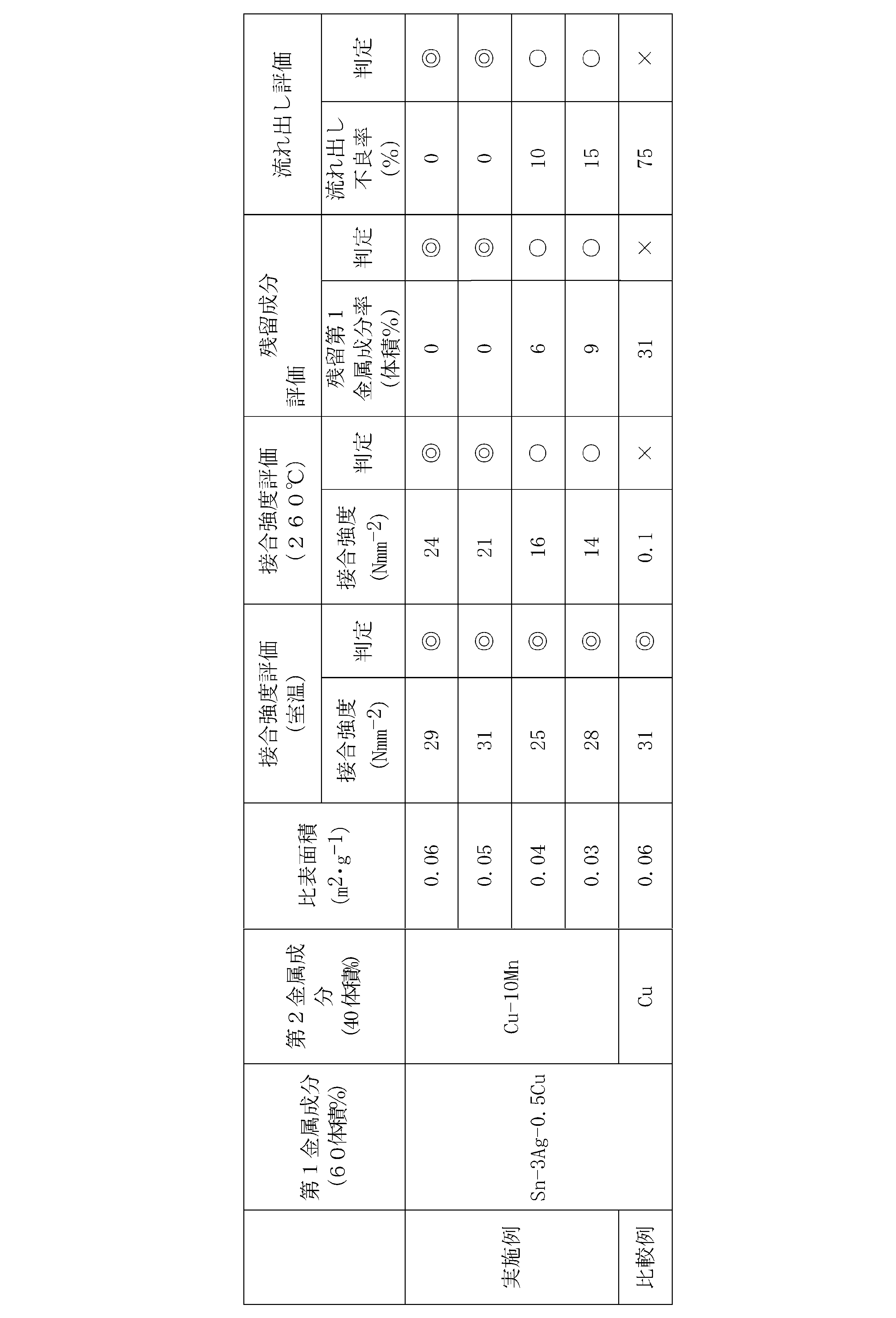
一方、260℃における接合強度についてみると、比較例では0.1Nmm-2と、2Nmm-2を大きく下回っており、接合強度が不十分であったのに対して、実施例では14~24Nmm-2と、2Nmm-2以上を保持し、実用強度を備えていることが確認された。さらに第二金属であるCu-10Mnの比表面積が0.05m2・g-1以上の場合に21Nmm-2以上を示し、特に高い耐熱強度を有した。
(b)SnめっきしたCu-10Mn合金とSn粉とCu-10Mn合金の混合体
(c)SnめっきしたCu-10Mn合金単体、
からなる金属粉とフラックスを混合することによりソルダペーストを作製した。
ただし、SnめっきしたCu-10Mn合金単体の場合は、Cu-Mn合金(第2金属)の合計比率を80%とした。
また、フラックスの配合割合は、ソルダペースト全体に占めるフラックスの割合が10重量%となるような割合とした。
なお、接合強度の評価、残留第1金属成分率、およびはんだ流れ出し不良率の評価にあたっては、上述の実施例2の場合と同様の基準で評価した。
表5に、各接合体の接合強度(室温、260℃)、残留第1金属成分率、はんだ流れ出し不良率、およびそれらの評価結果を示す。

一方、260℃における接合強度についてみると、比較例では0.1Nmm-2と、2Nmm-2を大きく下回っており、接合強度が不十分であったのに対して、実施例では24~26Nmm-2と、2Nmm-2以上を保持し、実用強度を備えていることが確認された。このことから、第1金属が第2金属の表面にめっき(コート)されている場合にも、上記の各実施例の場合と同様に、高い耐熱強度が得られることが確認された。
また、第2金属粉末として、Cu-10Mn合金の粉末を用意した。第2金属粉末の平均粒径は15μmとした。
フラックスとして、樹脂を添加したものと、樹脂を添加しなかったものを用意した。
フラックスA :30重量%
熱硬化性樹脂 :40重量%
硬化剤 :30重量%
フラックスA :30重量%
熱可塑性樹脂(ポリアミド樹脂) :70重量%
(1)樹脂を添加していない上記フラックスAをソルダペースト全体に占めるフラックスの割合が10重量%となるような割合で配合したソルダペーストと、
(2)熱硬化性樹脂配合フラックスBをソルダペースト全体に占めるフラックスの割合が25重量%となるような割合で配合したソルダペーストと、
(3)熱可塑性樹脂配合フラックスCをソルダペースト全体に占めるフラックスの割合が25重量%となるような割合で配合したソルダペーストと
を作製した。
表6に、各接合体の接合強度(室温、260℃)、残留第1金属成分率、はんだ流れ出し不良率、およびそれらの評価結果を示す。
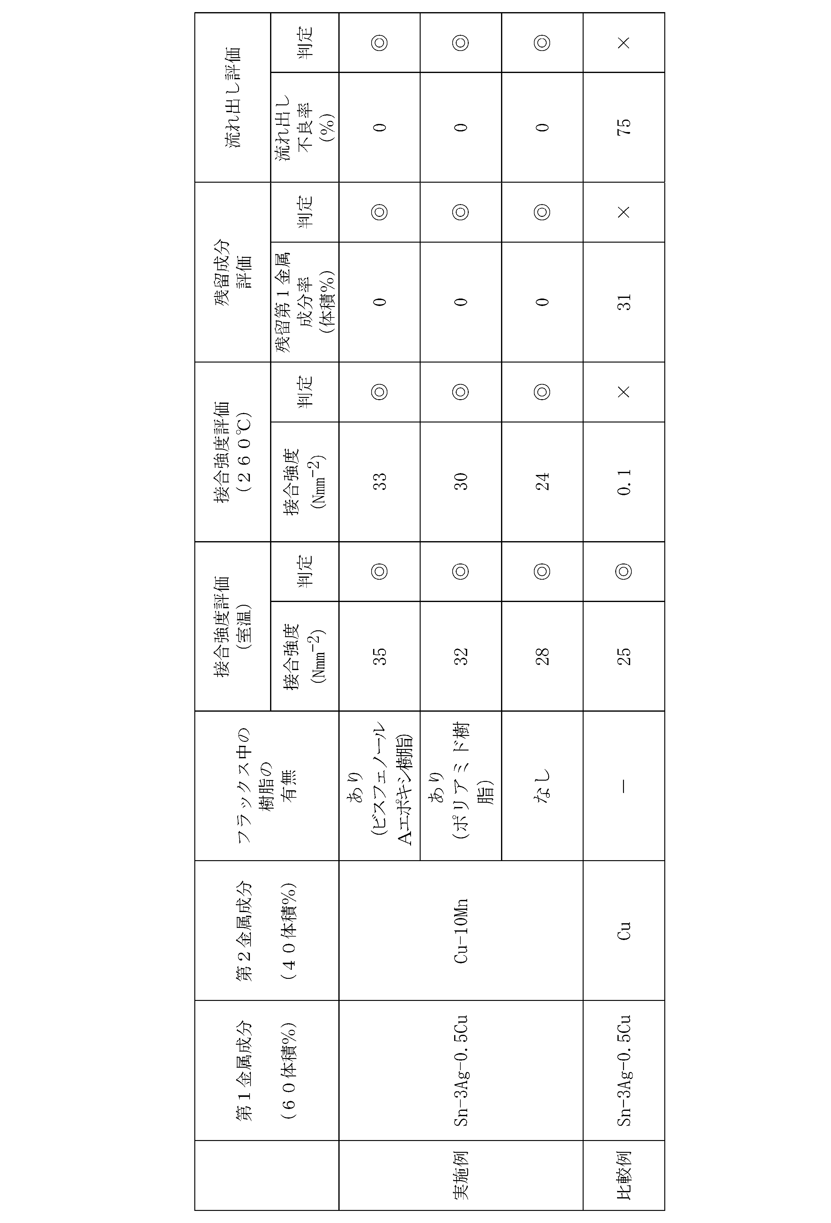
一方、260℃における接合強度についてみると、比較例では0.1Nmm-2と、2Nmm-2を大きく下回っており、接合強度が不十分であったのに対して、実施例では24~33Nmm-2と、2Nmm-2以上を保持し、実用強度を備えていることが確認された。
2 第2金属
3 金属間化合物
4 接合部
11a,11b 一対の電極(接合対象物)
10 ソルダペースト
Claims (12)
- 第1金属粉末と、前記第1金属粉末よりも融点の高い第2金属粉末とからなる金属成分と、フラックス成分とを含むソルダペーストであって、
前記第1金属はSnまたはSnを含む合金であり、
前記第2金属は、前記第1金属と、310℃以上の融点を示す金属間化合物を生成し、かつ、前記金属間化合物の格子定数と前記第2金属成分の格子定数との差である格子定数差が50%以上の金属または合金であること
を特徴とするソルダペースト。 - 前記金属成分中に占める前記第2金属粉末の割合が、30体積%以上であることを特徴とする請求項1記載のソルダペースト。
- 前記第1金属は、Sn単体、または、Cu、Ni、Ag、Au、Sb、Zn、Bi、In、Ge、Al、Co、Mn、Fe、Cr、Mg、Mn、Pd、Si、Sr、Te、Pからなる群より選ばれる少なくとも1種と、Snとを含む合金であること
を特徴とする請求項1または2記載のソルダペースト。 - 前記第2金属は、Cu-Mn合金またはCu-Ni合金であることを特徴とする請求項1~3のいずれかに記載のソルダペースト。
- 前記第2金属は、前記第2金属に占めるMnの割合が10~15重量%であるCu-Mn合金、または、前記第2金属に占めるNiの割合が10~15重量%であるCu-Ni合金であることを特徴とする請求項1~4のいずれかに記載のソルダペースト。
- 前記第2金属粉末は、比表面積が0.05m2・g-1以上のものであることを特徴とする請求項1~5のいずれかに記載のソルダペースト。
- 前記第1金属粉末のうち少なくとも一部が、前記第2金属粉末の周りにコートされていることを特徴とする請求項1~6のいずれかに記載のソルダペースト。
- 前記フラックスが、
(a)ロジン、重合ロジン、WW(water white)ロジン、水添ロジンからなるロジン群より選ばれる少なくとも1種、
(b)前記ロジン群より選ばれる少なくとも1種の誘導体を含むロジン系樹脂、
(c)硬化ヒマシ油、脂肪族アミド等のチキソ剤、有機酸、アミンのハロゲン化水素酸塩等の活性剤等の固体成分をエチレングリコールモノブチルエーテル、ジエチレングリコールモノエチルエーテル、ジエチレングリコールモノブチルエーテルからなる群より選ばれる少なくとも1種を溶剤で溶解してペースト状にしたもの
からなる群より選ばれる少なくとも1種を含むものであることを特徴とする請求項1~7のいずれかに記載のソルダペースト。 - 前記フラックスが、エポキシ樹脂、フェノール樹脂、ポリイミド樹脂、シリコン樹脂またはその変性樹脂、アクリル樹脂からなる熱硬化性樹脂群より選ばれる少なくとも1種、あるいは、ポリアミド樹脂、ポリスチレン樹脂、ポリメタクリル樹脂、ポリカーボネート樹脂、セルロース系樹脂からなる熱可塑性樹脂群から選ばれる少なくとも1種を含むものであることを特徴とする請求項1~8のいずれかに記載のソルダペースト。
- ソルダペーストを用いて接合対象物を接合する方法において、請求項1~9のいずれかに記載のソルダペーストを用い、加熱して前記ソルダペーストを構成する前記第1金属成分を、前記ソルダペーストを構成する前記第2金属との金属間化合物にして、接合対象物を接合させることを特徴とする接合方法。
- 接合対象物が、請求項1~9のいずれかに記載のソルダペーストを用いて接合された接合構造であって、
接合対象物を接合させている接合部のはんだは、前記ソルダペーストに由来する前記第2金属と、前記第2金属とSnとを含む金属間化合物とを主たる成分としており、前記ソルダペーストに由来する前記第1金属の金属成分全体に対する割合が30体積%以下であること
を特徴とする接合構造。 - 前記金属間化合物が、前記ソルダペーストに由来する前記第2金属であるCu-Mn合金、または、Cu-Ni合金と、前記ソルダペーストに由来する前記第1金属である、Sn単体、または、Cu、Ni、Ag、Au、Sb、Zn、Bi、In、Ge、Al、Co、Mn、Fe、Cr、Mg、Mn、Pd、Si、Sr、Te、Pからなる群より選ばれる少なくとも1種と、Snとを含む合金との間に形成された金属間化合物であることを特徴とする請求項11記載の接合構造。
Priority Applications (5)
| Application Number | Priority Date | Filing Date | Title |
|---|---|---|---|
| JP2011529863A JP5533876B2 (ja) | 2009-09-03 | 2010-08-12 | ソルダペースト、それを用いた接合方法、および接合構造 |
| KR1020127005180A KR101276147B1 (ko) | 2009-09-03 | 2010-08-12 | 솔더 페이스트, 그것을 사용한 접합 방법, 및 접합 구조 |
| TW99129327A TWI392557B (zh) | 2009-09-03 | 2010-08-31 | A solder paste, a joining method using it, and a bonding structure |
| US13/404,395 US9044816B2 (en) | 2009-09-03 | 2012-02-24 | Solder paste, joining method using the same and joined structure |
| US14/697,717 US10010980B2 (en) | 2009-09-03 | 2015-04-28 | Solder paste, joining method using the same and joined structure |
Applications Claiming Priority (2)
| Application Number | Priority Date | Filing Date | Title |
|---|---|---|---|
| JP2009-203611 | 2009-09-03 | ||
| JP2009203611 | 2009-09-03 |
Related Child Applications (1)
| Application Number | Title | Priority Date | Filing Date |
|---|---|---|---|
| US13/404,395 Continuation US9044816B2 (en) | 2009-09-03 | 2012-02-24 | Solder paste, joining method using the same and joined structure |
Publications (1)
| Publication Number | Publication Date |
|---|---|
| WO2011027659A1 true WO2011027659A1 (ja) | 2011-03-10 |
Family
ID=43649202
Family Applications (1)
| Application Number | Title | Priority Date | Filing Date |
|---|---|---|---|
| PCT/JP2010/063681 Ceased WO2011027659A1 (ja) | 2009-09-03 | 2010-08-12 | ソルダペースト、それを用いた接合方法、および接合構造 |
Country Status (5)
| Country | Link |
|---|---|
| US (2) | US9044816B2 (ja) |
| JP (1) | JP5533876B2 (ja) |
| KR (1) | KR101276147B1 (ja) |
| TW (1) | TWI392557B (ja) |
| WO (1) | WO2011027659A1 (ja) |
Cited By (36)
| Publication number | Priority date | Publication date | Assignee | Title |
|---|---|---|---|---|
| WO2012066795A1 (ja) * | 2010-11-19 | 2012-05-24 | 株式会社村田製作所 | 導電性材料、それを用いた接続方法、および接続構造 |
| CN102489897A (zh) * | 2011-11-16 | 2012-06-13 | 苏州之侨新材料科技有限公司 | 一种用于锡铋系的低温无铅焊锡助焊剂 |
| CN102513732A (zh) * | 2011-12-15 | 2012-06-27 | 中南大学 | 一种松香型无卤素免清洗助焊剂及其制备和应用 |
| CN102528327A (zh) * | 2011-12-30 | 2012-07-04 | 深圳市上煌实业有限公司 | 一种高温无铅焊锡膏及制备方法 |
| JP2012182293A (ja) * | 2011-03-01 | 2012-09-20 | Murata Mfg Co Ltd | 電子部品実装基板およびその製造方法 |
| JP2012182379A (ja) * | 2011-03-02 | 2012-09-20 | Murata Mfg Co Ltd | 多層チップ部品およびその製造方法 |
| JP2012250240A (ja) * | 2011-05-31 | 2012-12-20 | Asahi Kasei E-Materials Corp | 金属フィラー、はんだペースト、及び接続構造体 |
| CN102922162A (zh) * | 2012-11-01 | 2013-02-13 | 青岛英太克锡业科技有限公司 | 一种焊铝锡膏及其制备方法 |
| JP2013510240A (ja) * | 2009-11-05 | 2013-03-21 | オーメット サーキッツ インク | 冶金ネットワーク組成物の調製およびその使用方法 |
| WO2013038817A1 (ja) * | 2011-09-16 | 2013-03-21 | 株式会社村田製作所 | 導電性材料、それを用いた接続方法、および接続構造 |
| WO2013038816A1 (ja) * | 2011-09-16 | 2013-03-21 | 株式会社村田製作所 | 導電性材料、それを用いた接続方法、および接続構造 |
| WO2013132954A1 (ja) * | 2012-03-05 | 2013-09-12 | 株式会社村田製作所 | 接合方法、接合構造体およびその製造方法 |
| WO2013132942A1 (ja) * | 2012-03-05 | 2013-09-12 | 株式会社村田製作所 | 接合方法、接合構造体およびその製造方法 |
| WO2013132966A1 (ja) * | 2012-03-05 | 2013-09-12 | 株式会社村田製作所 | 電子部品および電子部品と接合対象物との接合構造体の形成方法 |
| JP2013258254A (ja) * | 2012-06-12 | 2013-12-26 | Koki:Kk | レーザー加熱工法による電子デバイスの製造方法 |
| CN103515343A (zh) * | 2012-06-22 | 2014-01-15 | 株式会社村田制作所 | 电子元器件模块及其制造方法 |
| JP2014007256A (ja) * | 2012-06-22 | 2014-01-16 | Murata Mfg Co Ltd | 配線基板およびその製造方法 |
| JP2014028380A (ja) * | 2012-07-31 | 2014-02-13 | Koki:Kk | 金属フィラー、はんだペースト、及び接続構造体 |
| TWI453087B (zh) * | 2012-11-22 | 2014-09-21 | Truan Sheng Lui | 光伏鋁銲帶 |
| KR20160006667A (ko) | 2013-05-10 | 2016-01-19 | 후지 덴키 가부시키가이샤 | 반도체 장치 및 반도체 장치의 제조방법 |
| JP2016069231A (ja) * | 2014-09-30 | 2016-05-09 | 株式会社村田製作所 | ステンドグラスの製造方法、ステンドグラス接合用の金属ペースト |
| CN105772979A (zh) * | 2016-04-13 | 2016-07-20 | 苏州伊飞特电子科技有限公司 | 一种高助焊剂环保型锡丝及其制备方法 |
| US9412517B2 (en) | 2012-03-05 | 2016-08-09 | Murata Manufacturing Co., Ltd. | Electronic part |
| CN105855748A (zh) * | 2016-04-27 | 2016-08-17 | 深圳市晨日科技股份有限公司 | 一种芯片封装固晶锡膏及其制备方法和使用工艺 |
| WO2016194435A1 (ja) * | 2015-06-01 | 2016-12-08 | 株式会社村田製作所 | 放熱部材の接合方法、放熱部材付き発熱素子 |
| EP2656955A4 (en) * | 2010-12-24 | 2017-07-19 | Murata Manufacturing Co., Ltd. | Bonding method, bonding structure, electronic device, manufacturing method for electronic device, and electronic component |
| CN107160052A (zh) * | 2017-04-12 | 2017-09-15 | 华南理工大学 | 一种高性能低温软钎焊无铅锡膏及其制备方法 |
| CN109483089A (zh) * | 2018-11-08 | 2019-03-19 | 云南锡业锡材有限公司 | 高温焊锡膏用助焊剂及其制备方法 |
| US10493567B2 (en) | 2017-05-11 | 2019-12-03 | Panasonic Intellectual Property Management Co., Ltd. | Solder alloy and bonded structure using the same |
| JP2020055032A (ja) * | 2018-09-28 | 2020-04-09 | 株式会社タムラ製作所 | 成形はんだ及び成形はんだの製造方法 |
| WO2021106056A1 (ja) * | 2019-11-26 | 2021-06-03 | 株式会社Fuji | 部品実装方法および部品実装システム |
| US20210197325A1 (en) * | 2018-11-29 | 2021-07-01 | Raytheon Company | Low cost approach for depositing solder and adhesives in a pattern for forming electronic assemblies |
| JP2022083853A (ja) * | 2020-11-25 | 2022-06-06 | パナソニックIpマネジメント株式会社 | 接合材料およびそれを用いる実装構造体 |
| JP2023524690A (ja) * | 2020-04-29 | 2023-06-13 | インディウム コーポレーション | 混合はんだ粉末を含む高温用途の無鉛はんだペースト |
| US11819915B2 (en) | 2015-05-29 | 2023-11-21 | Murata Manufacturing Co., Ltd. | Bonding member and bonding method |
| US11821058B2 (en) | 2014-09-10 | 2023-11-21 | Murata Manufacturing Co., Ltd. | Method for producing intermetallic compound |
Families Citing this family (31)
| Publication number | Priority date | Publication date | Assignee | Title |
|---|---|---|---|---|
| WO2011027659A1 (ja) * | 2009-09-03 | 2011-03-10 | 株式会社村田製作所 | ソルダペースト、それを用いた接合方法、および接合構造 |
| JP5146627B2 (ja) * | 2011-02-15 | 2013-02-20 | 株式会社村田製作所 | 多層配線基板およびその製造方法 |
| WO2013021567A1 (ja) * | 2011-08-11 | 2013-02-14 | 三洋電機株式会社 | 金属の接合方法および金属接合構造 |
| TWI467718B (zh) * | 2011-12-30 | 2015-01-01 | 財團法人工業技術研究院 | 凸塊結構以及電子封裝接點結構及其製造方法 |
| JP5978630B2 (ja) * | 2012-01-26 | 2016-08-24 | Tdk株式会社 | 電子回路モジュール部品及び電子回路モジュール部品の製造方法 |
| WO2014061085A1 (ja) * | 2012-10-15 | 2014-04-24 | 千住金属工業株式会社 | 低温ソルダペーストのはんだ付け方法 |
| CN105307812B (zh) * | 2013-04-09 | 2018-03-27 | 千住金属工业株式会社 | 焊膏 |
| WO2015089470A1 (en) * | 2013-12-13 | 2015-06-18 | Schlumberger Canada Limited | Tin-antimony-based high temperature solder for downhole components |
| KR20170011663A (ko) | 2015-07-23 | 2017-02-02 | 덕산하이메탈(주) | 발열 및 비정질 특성을 갖는 솔더 분말 제조 방법, 솔더 페이스트 제조 방법 및 솔더 페이스트를 이용한 저온 접합 방법 |
| JP6332566B2 (ja) * | 2015-09-15 | 2018-05-30 | 株式会社村田製作所 | 接合用部材、接合用部材の製造方法、および、接合方法 |
| JP6528852B2 (ja) | 2015-09-28 | 2019-06-12 | 株式会社村田製作所 | ヒートパイプ、放熱部品、ヒートパイプの製造方法 |
| US20170095891A1 (en) * | 2015-10-01 | 2017-04-06 | Iowa State University Research Foundation, Inc. | Lead-free composite solder |
| WO2017077824A1 (ja) * | 2015-11-05 | 2017-05-11 | 株式会社村田製作所 | 接合用部材、および、接合用部材の製造方法 |
| KR102101474B1 (ko) * | 2015-12-15 | 2020-04-16 | 주식회사 엘지화학 | 금속 페이스트 및 열전 모듈 |
| WO2017105011A1 (ko) * | 2015-12-15 | 2017-06-22 | 주식회사 엘지화학 | 금속 페이스트 및 열전 모듈 |
| WO2017119205A1 (ja) * | 2016-01-07 | 2017-07-13 | 株式会社村田製作所 | 金属組成物、金属間化合物部材、接合体 |
| JP5989928B1 (ja) | 2016-02-10 | 2016-09-07 | 古河電気工業株式会社 | 導電性接着フィルムおよびこれを用いたダイシング・ダイボンディングフィルム |
| JP5972490B1 (ja) | 2016-02-10 | 2016-08-17 | 古河電気工業株式会社 | 導電性接着剤組成物ならびにこれを用いた導電性接着フィルムおよびダイシング・ダイボンディングフィルム |
| JP5972489B1 (ja) | 2016-02-10 | 2016-08-17 | 古河電気工業株式会社 | 導電性接着フィルムおよびこれを用いたダイシング・ダイボンディングフィルム |
| JP6005312B1 (ja) | 2016-02-10 | 2016-10-12 | 古河電気工業株式会社 | 導電性接着フィルムおよびこれを用いたダイシング・ダイボンディングフィルム |
| JP6005313B1 (ja) * | 2016-02-10 | 2016-10-12 | 古河電気工業株式会社 | 導電性接着フィルムおよびこれを用いたダイシング・ダイボンディングフィルム |
| JP6160788B1 (ja) * | 2017-01-13 | 2017-07-12 | 千住金属工業株式会社 | フラックス |
| KR101888526B1 (ko) | 2017-08-28 | 2018-08-14 | 덕산하이메탈(주) | 발열 및 비정질 특성을 갖는 솔더 분말 제조 방법, 솔더 페이스트 제조 방법 및 솔더 페이스트를 이용한 저온 접합 방법 |
| TWI892959B (zh) * | 2017-12-07 | 2025-08-11 | 美商歐爾麥特電路有限公司 | 用於電子封裝總成之具有熱安定性微結構之冶金組合物及使用彼之方法 |
| JP7315377B2 (ja) | 2018-10-05 | 2023-07-26 | 株式会社Kelk | 熱電モジュール |
| US11581239B2 (en) * | 2019-01-18 | 2023-02-14 | Indium Corporation | Lead-free solder paste as thermal interface material |
| DE112020004146T5 (de) * | 2019-09-02 | 2022-05-25 | Nihon Superior Co., Ltd. | Lötpasten und lötstellen |
| WO2021177006A1 (ja) * | 2020-03-06 | 2021-09-10 | 三菱電機株式会社 | 薄板状接合部材およびその製造方法、半導体装置およびその製造方法、ならびに、電力変換装置 |
| CN111482734B (zh) * | 2020-04-21 | 2021-06-22 | 浙江力强科技有限公司 | 铜镍银钎焊浆料及其制备方法 |
| CN111745323B (zh) * | 2020-07-01 | 2022-03-25 | 云南锡业锡材有限公司 | 一种压力热熔焊接点涂锡膏用低固含量助焊剂及制备方法 |
| US20230137877A1 (en) * | 2021-11-02 | 2023-05-04 | Intel Corporation | No-remelt solder enforcement joint |
Citations (5)
| Publication number | Priority date | Publication date | Assignee | Title |
|---|---|---|---|---|
| JP2002254195A (ja) * | 2000-12-25 | 2002-09-10 | Tdk Corp | はんだ付け用組成物及びはんだ付け方法 |
| JP2002254194A (ja) * | 2000-06-12 | 2002-09-10 | Hitachi Ltd | 電子機器およびはんだ |
| JP2003094193A (ja) * | 2002-06-18 | 2003-04-02 | Matsushita Electric Ind Co Ltd | 鉛フリー半田ペースト |
| JP2003211289A (ja) * | 2002-01-21 | 2003-07-29 | Fujitsu Ltd | 導電性接合材料、それを用いた接合方法及び電子機器 |
| WO2007125861A1 (ja) * | 2006-04-26 | 2007-11-08 | Senju Metal Industry Co., Ltd. | ソルダペースト |
Family Cites Families (7)
| Publication number | Priority date | Publication date | Assignee | Title |
|---|---|---|---|---|
| US20020046627A1 (en) * | 1998-06-10 | 2002-04-25 | Hitoshi Amita | Solder powder, flux, solder paste, soldering method, soldered circuit board, and soldered joint product |
| JP3074649B1 (ja) * | 1999-02-23 | 2000-08-07 | インターナショナル・ビジネス・マシーンズ・コーポレ−ション | 無鉛半田粉末、無鉛半田ペースト、およびそれらの製造方法 |
| KR100867871B1 (ko) * | 2005-01-11 | 2008-11-07 | 가부시키가이샤 무라타 세이사쿠쇼 | 솔더 페이스트, 및 전자장치 |
| EP1952934B1 (en) * | 2005-11-11 | 2015-03-18 | Senju Metal Industry Co., Ltd. | Soldering paste and solder joints |
| CN1887500A (zh) * | 2006-06-20 | 2007-01-03 | 包德为 | 一种无铅焊锡膏 |
| US20100291399A1 (en) | 2006-09-01 | 2010-11-18 | Rikiya Kato | Lid for a functional part and a process for its manufacture |
| WO2011027659A1 (ja) * | 2009-09-03 | 2011-03-10 | 株式会社村田製作所 | ソルダペースト、それを用いた接合方法、および接合構造 |
-
2010
- 2010-08-12 WO PCT/JP2010/063681 patent/WO2011027659A1/ja not_active Ceased
- 2010-08-12 JP JP2011529863A patent/JP5533876B2/ja active Active
- 2010-08-12 KR KR1020127005180A patent/KR101276147B1/ko active Active
- 2010-08-31 TW TW99129327A patent/TWI392557B/zh active
-
2012
- 2012-02-24 US US13/404,395 patent/US9044816B2/en active Active
-
2015
- 2015-04-28 US US14/697,717 patent/US10010980B2/en active Active
Patent Citations (5)
| Publication number | Priority date | Publication date | Assignee | Title |
|---|---|---|---|---|
| JP2002254194A (ja) * | 2000-06-12 | 2002-09-10 | Hitachi Ltd | 電子機器およびはんだ |
| JP2002254195A (ja) * | 2000-12-25 | 2002-09-10 | Tdk Corp | はんだ付け用組成物及びはんだ付け方法 |
| JP2003211289A (ja) * | 2002-01-21 | 2003-07-29 | Fujitsu Ltd | 導電性接合材料、それを用いた接合方法及び電子機器 |
| JP2003094193A (ja) * | 2002-06-18 | 2003-04-02 | Matsushita Electric Ind Co Ltd | 鉛フリー半田ペースト |
| WO2007125861A1 (ja) * | 2006-04-26 | 2007-11-08 | Senju Metal Industry Co., Ltd. | ソルダペースト |
Cited By (60)
| Publication number | Priority date | Publication date | Assignee | Title |
|---|---|---|---|---|
| JP2013510240A (ja) * | 2009-11-05 | 2013-03-21 | オーメット サーキッツ インク | 冶金ネットワーク組成物の調製およびその使用方法 |
| WO2012066795A1 (ja) * | 2010-11-19 | 2012-05-24 | 株式会社村田製作所 | 導電性材料、それを用いた接続方法、および接続構造 |
| EP2656955A4 (en) * | 2010-12-24 | 2017-07-19 | Murata Manufacturing Co., Ltd. | Bonding method, bonding structure, electronic device, manufacturing method for electronic device, and electronic component |
| JP2012182293A (ja) * | 2011-03-01 | 2012-09-20 | Murata Mfg Co Ltd | 電子部品実装基板およびその製造方法 |
| JP2012182379A (ja) * | 2011-03-02 | 2012-09-20 | Murata Mfg Co Ltd | 多層チップ部品およびその製造方法 |
| JP2012250240A (ja) * | 2011-05-31 | 2012-12-20 | Asahi Kasei E-Materials Corp | 金属フィラー、はんだペースト、及び接続構造体 |
| WO2013038817A1 (ja) * | 2011-09-16 | 2013-03-21 | 株式会社村田製作所 | 導電性材料、それを用いた接続方法、および接続構造 |
| JPWO2013038816A1 (ja) * | 2011-09-16 | 2015-03-26 | 株式会社村田製作所 | 導電性材料、それを用いた接続方法、および接続構造 |
| WO2013038816A1 (ja) * | 2011-09-16 | 2013-03-21 | 株式会社村田製作所 | 導電性材料、それを用いた接続方法、および接続構造 |
| CN102489897B (zh) * | 2011-11-16 | 2013-08-07 | 苏州之侨新材料科技有限公司 | 一种用于锡铋系的低温无铅焊锡助焊剂 |
| CN102489897A (zh) * | 2011-11-16 | 2012-06-13 | 苏州之侨新材料科技有限公司 | 一种用于锡铋系的低温无铅焊锡助焊剂 |
| CN102513732A (zh) * | 2011-12-15 | 2012-06-27 | 中南大学 | 一种松香型无卤素免清洗助焊剂及其制备和应用 |
| CN102528327A (zh) * | 2011-12-30 | 2012-07-04 | 深圳市上煌实业有限公司 | 一种高温无铅焊锡膏及制备方法 |
| TWI505899B (zh) * | 2012-03-05 | 2015-11-01 | 村田製作所股份有限公司 | A bonding method, a bonding structure, and a method for manufacturing the same |
| WO2013132954A1 (ja) * | 2012-03-05 | 2013-09-12 | 株式会社村田製作所 | 接合方法、接合構造体およびその製造方法 |
| CN104160463B (zh) * | 2012-03-05 | 2017-09-29 | 株式会社村田制作所 | 电子部件及电子部件与接合对象物的接合结构体的形成方法 |
| US9412517B2 (en) | 2012-03-05 | 2016-08-09 | Murata Manufacturing Co., Ltd. | Electronic part |
| US9333593B2 (en) | 2012-03-05 | 2016-05-10 | Murata Manufacturing Co., Ltd. | Joining method, joint structure and method for producing the same |
| WO2013132966A1 (ja) * | 2012-03-05 | 2013-09-12 | 株式会社村田製作所 | 電子部品および電子部品と接合対象物との接合構造体の形成方法 |
| US9691546B2 (en) | 2012-03-05 | 2017-06-27 | Murata Manufacturing Co., Ltd. | Electronic part and method for forming joint structure of electronic part and joining object |
| JPWO2013132966A1 (ja) * | 2012-03-05 | 2015-07-30 | 株式会社村田製作所 | 電子部品および電子部品と接合対象物との接合構造体の形成方法 |
| CN104160463A (zh) * | 2012-03-05 | 2014-11-19 | 株式会社村田制作所 | 电子部件及电子部件与接合对象物的接合结构体的形成方法 |
| WO2013132942A1 (ja) * | 2012-03-05 | 2013-09-12 | 株式会社村田製作所 | 接合方法、接合構造体およびその製造方法 |
| JPWO2013132942A1 (ja) * | 2012-03-05 | 2015-07-30 | 株式会社村田製作所 | 接合方法、接合構造体およびその製造方法 |
| JPWO2013132954A1 (ja) * | 2012-03-05 | 2015-07-30 | 株式会社村田製作所 | 接合方法、接合構造体およびその製造方法 |
| JP2013258254A (ja) * | 2012-06-12 | 2013-12-26 | Koki:Kk | レーザー加熱工法による電子デバイスの製造方法 |
| US9113571B2 (en) | 2012-06-22 | 2015-08-18 | Murata Manufacturing Co., Ltd. | Electronic component module and method for manufacturing the same |
| JP2014007227A (ja) * | 2012-06-22 | 2014-01-16 | Murata Mfg Co Ltd | 電子部品モジュールおよびその製造方法 |
| JP2014007256A (ja) * | 2012-06-22 | 2014-01-16 | Murata Mfg Co Ltd | 配線基板およびその製造方法 |
| CN103515343A (zh) * | 2012-06-22 | 2014-01-15 | 株式会社村田制作所 | 电子元器件模块及其制造方法 |
| JP2014028380A (ja) * | 2012-07-31 | 2014-02-13 | Koki:Kk | 金属フィラー、はんだペースト、及び接続構造体 |
| CN102922162A (zh) * | 2012-11-01 | 2013-02-13 | 青岛英太克锡业科技有限公司 | 一种焊铝锡膏及其制备方法 |
| TWI453087B (zh) * | 2012-11-22 | 2014-09-21 | Truan Sheng Lui | 光伏鋁銲帶 |
| KR20160006667A (ko) | 2013-05-10 | 2016-01-19 | 후지 덴키 가부시키가이샤 | 반도체 장치 및 반도체 장치의 제조방법 |
| US10157877B2 (en) | 2013-05-10 | 2018-12-18 | Fuji Electric Co., Ltd. | Semiconductor device and manufacturing method of semiconductor device |
| US11821058B2 (en) | 2014-09-10 | 2023-11-21 | Murata Manufacturing Co., Ltd. | Method for producing intermetallic compound |
| JP2016069231A (ja) * | 2014-09-30 | 2016-05-09 | 株式会社村田製作所 | ステンドグラスの製造方法、ステンドグラス接合用の金属ペースト |
| US11819915B2 (en) | 2015-05-29 | 2023-11-21 | Murata Manufacturing Co., Ltd. | Bonding member and bonding method |
| WO2016194435A1 (ja) * | 2015-06-01 | 2016-12-08 | 株式会社村田製作所 | 放熱部材の接合方法、放熱部材付き発熱素子 |
| CN105772979A (zh) * | 2016-04-13 | 2016-07-20 | 苏州伊飞特电子科技有限公司 | 一种高助焊剂环保型锡丝及其制备方法 |
| CN105855748B (zh) * | 2016-04-27 | 2017-02-08 | 深圳市晨日科技股份有限公司 | 一种芯片封装固晶锡膏及其制备方法和使用工艺 |
| CN105855748A (zh) * | 2016-04-27 | 2016-08-17 | 深圳市晨日科技股份有限公司 | 一种芯片封装固晶锡膏及其制备方法和使用工艺 |
| CN107160052A (zh) * | 2017-04-12 | 2017-09-15 | 华南理工大学 | 一种高性能低温软钎焊无铅锡膏及其制备方法 |
| CN107160052B (zh) * | 2017-04-12 | 2019-05-14 | 华南理工大学 | 一种高性能低温软钎焊无铅锡膏及其制备方法 |
| US10493567B2 (en) | 2017-05-11 | 2019-12-03 | Panasonic Intellectual Property Management Co., Ltd. | Solder alloy and bonded structure using the same |
| JP7229220B2 (ja) | 2018-09-28 | 2023-02-27 | 株式会社タムラ製作所 | 成形はんだ |
| JP2020055032A (ja) * | 2018-09-28 | 2020-04-09 | 株式会社タムラ製作所 | 成形はんだ及び成形はんだの製造方法 |
| JP2021037551A (ja) * | 2018-09-28 | 2021-03-11 | 株式会社タムラ製作所 | 成形はんだ |
| CN109483089B (zh) * | 2018-11-08 | 2021-04-30 | 云南锡业锡材有限公司 | 高温焊锡膏用助焊剂及其制备方法 |
| CN109483089A (zh) * | 2018-11-08 | 2019-03-19 | 云南锡业锡材有限公司 | 高温焊锡膏用助焊剂及其制备方法 |
| US20210197325A1 (en) * | 2018-11-29 | 2021-07-01 | Raytheon Company | Low cost approach for depositing solder and adhesives in a pattern for forming electronic assemblies |
| US12564908B2 (en) * | 2018-11-29 | 2026-03-03 | Raytheon Company | Low cost approach for depositing solder and adhesives in a pattern for forming electronic assemblies |
| JPWO2021106056A1 (ja) * | 2019-11-26 | 2021-06-03 | ||
| CN114728359A (zh) * | 2019-11-26 | 2022-07-08 | 株式会社富士 | 元件安装方法及元件安装系统 |
| WO2021106056A1 (ja) * | 2019-11-26 | 2021-06-03 | 株式会社Fuji | 部品実装方法および部品実装システム |
| JP7337188B2 (ja) | 2019-11-26 | 2023-09-01 | 株式会社Fuji | 部品実装方法および部品実装システム |
| JP2023524690A (ja) * | 2020-04-29 | 2023-06-13 | インディウム コーポレーション | 混合はんだ粉末を含む高温用途の無鉛はんだペースト |
| JP7704777B2 (ja) | 2020-04-29 | 2025-07-08 | インディウム コーポレーション | 混合はんだ粉末を含む高温用途の無鉛はんだペースト |
| JP2022083853A (ja) * | 2020-11-25 | 2022-06-06 | パナソニックIpマネジメント株式会社 | 接合材料およびそれを用いる実装構造体 |
| JP7653601B2 (ja) | 2020-11-25 | 2025-03-31 | パナソニックIpマネジメント株式会社 | 接合材料およびそれを用いる実装構造体 |
Also Published As
| Publication number | Publication date |
|---|---|
| TWI392557B (zh) | 2013-04-11 |
| JP5533876B2 (ja) | 2014-06-25 |
| US20120156512A1 (en) | 2012-06-21 |
| US9044816B2 (en) | 2015-06-02 |
| TW201124224A (en) | 2011-07-16 |
| US20150239069A1 (en) | 2015-08-27 |
| KR101276147B1 (ko) | 2013-06-18 |
| KR20120048662A (ko) | 2012-05-15 |
| US10010980B2 (en) | 2018-07-03 |
| JPWO2011027659A1 (ja) | 2013-02-04 |
Similar Documents
| Publication | Publication Date | Title |
|---|---|---|
| JP5533876B2 (ja) | ソルダペースト、それを用いた接合方法、および接合構造 | |
| JP5754480B2 (ja) | 接続対象物の接続方法および電子装置の製造方法 | |
| WO2013038817A1 (ja) | 導電性材料、それを用いた接続方法、および接続構造 | |
| WO2013038816A1 (ja) | 導電性材料、それを用いた接続方法、および接続構造 | |
| JP4613823B2 (ja) | ソルダペーストおよびプリント基板 | |
| CN103168392B (zh) | 连接结构 | |
| JP5067163B2 (ja) | ソルダペーストとはんだ継手 | |
| JP2014008523A (ja) | はんだ合金、ソルダペーストおよび電子回路基板 | |
| JP6683244B2 (ja) | 接合材料及び接合体の製造方法 | |
| JP5115915B2 (ja) | 鉛フリーはんだ、そのはんだ加工物、ソルダーペースト及び電子部品はんだ付け基板 | |
| JP5481753B2 (ja) | フラックス組成物及びはんだペースト組成物 | |
| JP2021133410A (ja) | 導電性接合材料および導電性接合体 |
Legal Events
| Date | Code | Title | Description |
|---|---|---|---|
| 121 | Ep: the epo has been informed by wipo that ep was designated in this application |
Ref document number: 10813610 Country of ref document: EP Kind code of ref document: A1 |
|
| WWE | Wipo information: entry into national phase |
Ref document number: 2011529863 Country of ref document: JP |
|
| ENP | Entry into the national phase |
Ref document number: 20127005180 Country of ref document: KR Kind code of ref document: A |
|
| NENP | Non-entry into the national phase |
Ref country code: DE |
|
| 122 | Ep: pct application non-entry in european phase |
Ref document number: 10813610 Country of ref document: EP Kind code of ref document: A1 |