WO2010110281A1 - ヒートシンク一体化パッケージ及びその製造方法 - Google Patents
ヒートシンク一体化パッケージ及びその製造方法 Download PDFInfo
- Publication number
- WO2010110281A1 WO2010110281A1 PCT/JP2010/055014 JP2010055014W WO2010110281A1 WO 2010110281 A1 WO2010110281 A1 WO 2010110281A1 JP 2010055014 W JP2010055014 W JP 2010055014W WO 2010110281 A1 WO2010110281 A1 WO 2010110281A1
- Authority
- WO
- WIPO (PCT)
- Prior art keywords
- heat sink
- wiring
- substrate
- integrated package
- electronic component
- Prior art date
- Legal status (The legal status is an assumption and is not a legal conclusion. Google has not performed a legal analysis and makes no representation as to the accuracy of the status listed.)
- Ceased
Links
Images






Classifications
-
- H—ELECTRICITY
- H10—SEMICONDUCTOR DEVICES; ELECTRIC SOLID-STATE DEVICES NOT OTHERWISE PROVIDED FOR
- H10W—GENERIC PACKAGES, INTERCONNECTIONS, CONNECTORS OR OTHER CONSTRUCTIONAL DETAILS OF DEVICES COVERED BY CLASS H10
- H10W90/00—Package configurations
- H10W90/701—Package configurations characterised by the relative positions of pads or connectors relative to package parts
-
- H—ELECTRICITY
- H10—SEMICONDUCTOR DEVICES; ELECTRIC SOLID-STATE DEVICES NOT OTHERWISE PROVIDED FOR
- H10W—GENERIC PACKAGES, INTERCONNECTIONS, CONNECTORS OR OTHER CONSTRUCTIONAL DETAILS OF DEVICES COVERED BY CLASS H10
- H10W40/00—Arrangements for thermal protection or thermal control
- H10W40/20—Arrangements for cooling
- H10W40/22—Arrangements for cooling characterised by their shape, e.g. having conical or cylindrical projections
-
- H—ELECTRICITY
- H10—SEMICONDUCTOR DEVICES; ELECTRIC SOLID-STATE DEVICES NOT OTHERWISE PROVIDED FOR
- H10W—GENERIC PACKAGES, INTERCONNECTIONS, CONNECTORS OR OTHER CONSTRUCTIONAL DETAILS OF DEVICES COVERED BY CLASS H10
- H10W40/00—Arrangements for thermal protection or thermal control
- H10W40/70—Fillings or auxiliary members in containers or in encapsulations for thermal protection or control
- H10W40/77—Auxiliary members characterised by their shape
- H10W40/778—Auxiliary members characterised by their shape in encapsulations
-
- H—ELECTRICITY
- H10—SEMICONDUCTOR DEVICES; ELECTRIC SOLID-STATE DEVICES NOT OTHERWISE PROVIDED FOR
- H10W—GENERIC PACKAGES, INTERCONNECTIONS, CONNECTORS OR OTHER CONSTRUCTIONAL DETAILS OF DEVICES COVERED BY CLASS H10
- H10W70/00—Package substrates; Interposers; Redistribution layers [RDL]
- H10W70/01—Manufacture or treatment
- H10W70/05—Manufacture or treatment of insulating or insulated package substrates, or of interposers, or of redistribution layers
- H10W70/098—Applying pastes or inks, e.g. screen printing
-
- H—ELECTRICITY
- H10—SEMICONDUCTOR DEVICES; ELECTRIC SOLID-STATE DEVICES NOT OTHERWISE PROVIDED FOR
- H10W—GENERIC PACKAGES, INTERCONNECTIONS, CONNECTORS OR OTHER CONSTRUCTIONAL DETAILS OF DEVICES COVERED BY CLASS H10
- H10W90/00—Package configurations
- H10W90/701—Package configurations characterised by the relative positions of pads or connectors relative to package parts
- H10W90/721—Package configurations characterised by the relative positions of pads or connectors relative to package parts of bump connectors
- H10W90/724—Package configurations characterised by the relative positions of pads or connectors relative to package parts of bump connectors between a chip and a stacked insulating package substrate, interposer or RDL
-
- Y—GENERAL TAGGING OF NEW TECHNOLOGICAL DEVELOPMENTS; GENERAL TAGGING OF CROSS-SECTIONAL TECHNOLOGIES SPANNING OVER SEVERAL SECTIONS OF THE IPC; TECHNICAL SUBJECTS COVERED BY FORMER USPC CROSS-REFERENCE ART COLLECTIONS [XRACs] AND DIGESTS
- Y10—TECHNICAL SUBJECTS COVERED BY FORMER USPC
- Y10T—TECHNICAL SUBJECTS COVERED BY FORMER US CLASSIFICATION
- Y10T29/00—Metal working
- Y10T29/49—Method of mechanical manufacture
- Y10T29/49002—Electrical device making
- Y10T29/49117—Conductor or circuit manufacturing
- Y10T29/49124—On flat or curved insulated base, e.g., printed circuit, etc.
- Y10T29/4913—Assembling to base an electrical component, e.g., capacitor, etc.
Definitions
- the present invention relates to a heat sink integrated package in which electronic components are mounted on a heat sink substrate, and a manufacturing method thereof.
- FIG. 16 is a cross-sectional view showing a flat heat pipe structure formed of a thin plate-like member disclosed in Patent Document 1.
- the illustrated heat pipe structure the lower member, the lower intermediate plate, the upper intermediate plate, and the upper member are in an integrated state by directly joining their peripheral portions.
- the refrigerant injection hole and the air discharge hole are closed.
- the refrigerant absorbs heat from the device to be cooled mounted on the printed circuit board, and the refrigerant is warmed and evaporated by this, the vapor diffuses to the peripheral side and the heat is dissipated at the peripheral part of the heat pipe. Condensate.
- the illustrated heat pipe structure is a wick structure that is laminated in a mesh shape so as to cause capillary action.
- an electrode for external connection is provided on the back surface of the printed wiring board.
- the heat sink is required to have a technique for facilitating wiring to the external electrode provided on the opposite side surface.
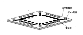
- Patent Document 2 discloses a post electrode part with wiring created by an electroforming method described later.
- the heat sink is used as a mounting substrate for the LSI chip, so that the LSI chip mounting substrate is not required in addition to the heat sink, and a through hole is formed in the mounting substrate to form a metal material. It is an object to easily take out an external electrode without the need for through wiring technology for filling.
- the present invention provides a simpler heat sink device that has a configuration for radiating heat further from the heat sink and can obtain a large cooling effect without heat being trapped inside the housing. It is aimed.
- the heat sink substrate has a structure in which at least one metal plate is laminated, and the metal plate is extended to be generated from the electronic component.
- a thermal connector is formed that releases heat from there.
- An electronic component is mounted on the heat sink substrate on which the wiring is formed, and the electrode terminal of the electronic component and a necessary portion of the wiring are electrically connected.
- a post electrode part with wiring having a horizontal wiring portion and a post electrode is attached to the wiring on the heat sink substrate, and an external electrode connected to the horizontal wiring portion is formed.
- the heat sink substrate has a structure in which at least one metal plate is laminated, the metal plate is extended, A thermal connector that releases heat generated from the electronic component to the outside is formed.
- An electronic component is mounted on the heat sink substrate on which the wiring is formed, and the electrode terminal of the electronic component and a necessary portion of the wiring are electrically connected.
- a post electrode part with wiring constituted by integrally connecting a horizontal wiring portion and a post electrode by a support plate is mounted on a heat sink substrate and connected to the wiring on the heat sink substrate. After resin sealing, the support plate is peeled off, and external electrodes connected to the horizontal wiring portion exposed by the peeling are formed.
- the support plate of the post electrode part with wiring has an insulating base tape affixed to the support plate, and the insulating base tape exposed by peeling the support plate functions as a protective film so that the external electrode and the horizontal wiring
- the parts are connected through holes formed in the protective film.
- the wiring on the heat sink substrate is formed by attaching a tape material with a metal film on the heat sink substrate and patterning the metal film by lithography and etching.
- the heat sink integrated package by attaching the heat sink itself as the LSI chip mounting substrate, no LSI chip mounting substrate is required other than the heat sink, and through holes are formed in the mounting substrate.
- the external electrode can be easily taken out without the need for the through wiring technique for filling the metal material.
- a structure for radiating heat further from the heat sink is provided, and a large cooling effect can be obtained without heat being trapped inside the housing.
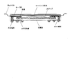
- FIG. 1 It is sectional drawing which shows the whole structure of the heat sink integrated package of 1st Embodiment which actualized this invention.
- (A) is sectional drawing shown in the state which mounted
- (B) is the perspective view.
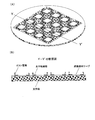
- (A) is a perspective view showing post electrode parts with wiring shown in a state where a large number of them are integrally connected, and (B) shows a cross-sectional view taken along the line Y-Y 'in the figure. It is a perspective view which shows the post electrode component with a wiring disclosed by patent document 2.
- FIG. 1 is a plan view in a state of being attached, and (B) is a cross-sectional view taken along the line Q-Q ′.
- (A) is a plan view showing a completed heat sink substrate, and (B) is a cross-sectional view taken along the line R-R ′.
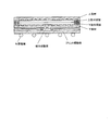
- FIG. 1 is a cross-sectional view showing the overall configuration of a heat sink integrated package of a first embodiment embodying the present invention.
- An electrode terminal of an electronic component such as an LSI chip is electrically connected to a necessary portion of the wiring on a heat sink substrate on which wiring is formed via a tape material.
- heat sink substrate used in the present specification means a substrate having not only a heat sink function but also a function as a mounting substrate for an electronic component such as an LSI chip mounted thereon. .
- This heat sink substrate is made by laminating at least one metal plate (copper plate) and extending the laminated plate left and right or front and rear and left and right, and using it as a wing, heat is transferred from there to an external housing, etc.
- the heat sink substrate configuration itself can have any shape and configuration.
- a structure in which a plurality of metal plates are bonded together can be used, and a heat pipe structure or a wick structure described as the prior art with reference to FIG. It is also possible to form a laminate.
- a copper plate is laminated on the side opposite to the LSI chip mounting surface (upper surface), and is extended to the left and right.
- Post electrode parts with wiring are attached to the wiring on the heat sink substrate.
- the post electrode part with wiring is a horizontal wiring part by a support part constituted by a support plate and an insulating base tape attached to the support plate. And the post electrode are integrally connected.
- the support plate is peeled off.
- FIG. 1 it has shown in the state after peeling.
- the insulating base tape exposed by peeling functions as a protective film.
- a hole is formed in the protective film to form an external electrode (bump electrode) connected to the horizontal wiring portion.
- FIGS. 2A is a cross-sectional view showing an electronic component such as an LSI chip mounted on a heat sink substrate having wiring
- FIG. 2B is a perspective view thereof.
- Wiring is provided on the front surface of the heat sink substrate via a tape material.
- An electrode terminal of an electronic component such as an LSI chip and a necessary portion of the wiring pattern are electrically connected on the heat sink substrate on which the wiring is formed in this way. That is, an electronic component is bonded to a heat sink substrate having a wiring pattern with a die bond material and mounted by a flip chip method. Alternatively, it can be connected to the wiring pattern by a bonding wire (wire bond connection method).
- the manufacture of the heat sink substrate is actually assembled on a heat sink substrate in a state where a large number of the heat sink substrates are integrally connected, and the heat sink is integrated. After the assembly of the package is completed, the individual chips are cut into individual chips.
- FIG. 3 is a view showing post electrode parts with wiring
- FIG. 3A is a perspective view showing post electrode parts with wiring shown in a state where a large number of post electrode parts are connected together.
- a cross-sectional view taken along line (B) is shown in FIG.
- a support portion a tape made of an insulating base material of a thin film typified by polyimide tape or the like on a whole surface of one side of a supporting plate (for example, stainless steel plate, silicon substrate or glass) or copper foil on the insulating base material Use tape with attached tape.
- This insulating base tape functions as a protective film that covers the wiring layer in the finished product.
- the support plate is peeled off from the insulating base tape in a later step.
- an ultraviolet peeling adhesive is used as an adhesive that easily peels off at high temperature or an adhesive with a heat capsule, or a material that transmits light (such as heat resistant low thermal expansion glass) as a support portion.
- a thermoplastic adhesive may be used.
- a metal seed layer to be a wiring pattern (horizontal wiring portion) is formed on this tape to form a metal-attached tape.
- the seed layer for example, gold, silver, copper, or palladium foil that enables copper plating can be used.
- the pattern of the horizontal wiring portion is completed by applying a resist on the seed layer, exposing and developing the pattern, further etching, removing the resist.
- a wiring layer is grown on the seed layer by plating. Further thereon, resist application and development are performed to form a post electrode portion, and the post portion is plated and grown.
- the horizontal wiring part may be patterned directly with nano metal particles to omit the lithography process. In the same manner as described above, a resist is applied and developed to form a post electrode portion, and the post portion is plated and grown. Thus, the post electrode part with wiring is completed.
- a horizontal wiring pattern can also be formed by lithography on the copper foil. Further thereon, resist application and development are performed to form a post electrode portion, and the post portion is plated and grown. Thus, the post electrode part with wiring is completed.
- FIG. 4 is a perspective view showing the post electrode part with wiring disclosed in Patent Document 2.
- FIG. 4 instead of the post electrode part with wiring described above, a known part as disclosed in Patent Document 2 can be used.
- a wiring pattern (horizontal wiring portion) is formed on a support plate to be peeled off in a later process by, for example, electroforming, and the wiring pattern is formed.
- FIG. 5 is a cross-sectional view showing a state in which post electrode parts with wiring as shown in FIG. 3 or FIG. 4 are arranged on a heat sink substrate on which an LSI chip is mounted.
- FIG. 6 is a diagram showing a state in which post electrode parts with wiring are connected and fixed on the heat sink substrate. At predetermined positions of the wiring formed on the heat sink substrate, post electrode parts with wiring integrally connected by a support plate are fixed together and electrically connected.
- the post electrode component side can be formed by a method of providing a convex portion and inserting and crimping or inserting and crimping. At the stage where the post electrodes are fixed at predetermined positions on the wiring pattern, all the post electrodes are integrally connected by a plate-like support plate.
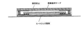
- FIG. 7 is a view showing a state where the resin is sealed after fixing the post electrode. Although the figure shows only one part, in reality, a large number of parts are connected and placed in a mold and filled with resin. Thus, transfer molding is performed so as to fill a space between the heat sink substrate and the insulating base tape, or resin sealing is performed using a liquid resin (a material is, for example, an epoxy type).
- a liquid resin a material is, for example, an epoxy type
- FIG. 8 is a diagram showing the state after the support plate is peeled off. By peeling the support plate, the insulating base tape covering the wiring layer is exposed. This insulating base tape functions as a protective film for the finished product.
- FIG. 9 is a cross-sectional view showing the overall configuration of the heat sink integrated package of the second embodiment embodying the present invention. Only the configuration of the heat sink substrate is different from that of the first embodiment.
- the illustrated heat sink substrate has a structure in which at least one metal plate (copper plate) is laminated, and a part of the laminated plate is extended left and right, front and rear, left and right, A thermal connector that releases heat from there to an external housing or the like is formed like a wing, but in the example shown, the plate on the side close to the LSI chip mounting surface (bottom surface) is extended. .
- wiring is provided on the lowermost surface of the heat sink substrate via a tape material.
- the exemplary heat sink substrate corresponds to the second embodiment described above in which the plate on the side close to the LSI chip mounting surface is extended. However, in the manufacturing technique described below, the position of the metal plate to be laminated is placed on the LSI chip mounting surface. Only by changing to the far side, a heat sink substrate that can be used in the first embodiment described above can be manufactured.
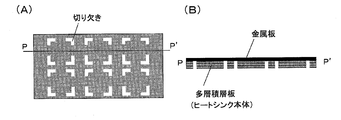
- FIG. 10A is a plan view of a multilayer laminate (heat sink body) with a metal plate attached
- FIG. 10B is a cross-sectional view taken along the line PP ′.
- the heat sink main body is exemplified as a multilayer laminated plate in which a plurality of metal plates are bonded together, but the present invention is not limited to the multilayer laminated plate, and the heat pipe structure or the conventional technology described with reference to FIG. Any shape and configuration including a wick structure (laminated in a mesh form to cause capillary action) can be used.
- a hanging portion that can be easily cut later is attached, and a plurality of packages are stacked as a single plate.
- a single metal plate (copper plate) is bonded to the uppermost surface (or lowermost surface) of such a heat sink body using, for example, an adhesive (in this specification, a heat sink body and a metal plate bonded to the metal plate are bonded to each other).
- the combination is called a heat sink).
- the laminated plate to be bonded is cut by cutting the four corners of each package in advance.
- a connector can be formed (see FIG. 12A).
- FIG. 12A the case where thermal connectors extended to the four sides on the front, rear, left and right in the figure are illustrated, but it is not always necessary to provide the front, rear, left and right, only two opposite sides (left and right or front and rear in the figure) or one side But it is possible.
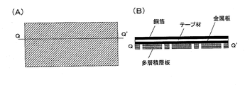
- FIG. 11A is a plan view in a state of being attached
- FIG. 11B is a cross-sectional view taken along the line Q-Q ′.
- a tape material with copper foil a metal film having a low resistance to be a wiring pattern is deposited or pasted on the entire surface of the thin film tape to form a tape with metal.
- an insulating base material of a thin film represented by a polyimide tape or the like is desirable.
- the metal film for example, gold, silver, copper, or palladium foil can be used.
- a thin film tape and a thin metal film (for example, copper foil) integrated may be used.
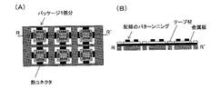
- FIG. 12A is a plan view showing the heat sink substrate completed in a connected state
- FIG. 12B is a cross-sectional view taken along the line R-R ′.
- a resist is applied on the metal layer (copper foil), the pattern is exposed and developed, and further etched, and the resist is removed to complete the wiring pattern.
- a heat sink integrated package is assembled in a later process on the heat sink substrates in a state where a plurality of them are connected in this way, and after completion, they are separated into individual substrates.
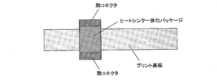
- FIG. 13 is a diagram for explaining an example of how to use the thermal connector of the heat sink integrated package.
- the heat sink integrated package of the second embodiment described above is mounted together with electronic circuit elements such as resistors, ICs, capacitors and connectors.
- This printed circuit board is fixed to the housing.
- the housing itself can be configured similarly to the heat sink substrate described above. That is, the illustrated case has a structure in which a single copper plate is laminated, and the printed board mounting portion is configured by stretching the single copper plate and bending the stretched portion into a predetermined shape. Yes.
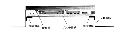
- FIG. 14 is a diagram showing a state after mounting and fixing.
- the printed circuit board is fixed to the casing extension part, and the thermal connector of the heat sink integrated package is fixed to the casing lamination part at the connection part.
- the printed circuit board is fixed to the housing extension by screwing or the like using a fixing jig as shown.
- the heat sink integrated package can be fixed to the housing laminated portion of the thermal connector by screwing, insertion, caulking, or the like.
- the insertion means that an insertion port is provided in advance on the housing side, and the connector portion is inserted therein, and the caulking means that the connector portion and the housing portion are pressed together so that an uneven portion can be formed at the same time. It is to be.
- the heat connector of the heat sink integrated package can be configured to protrude from the side surface of the substrate.
- FIG. 15 is a view of the printed circuit board on which the heat sink integrated package is mounted as viewed from above. When the thermal connector protrudes from both sides of the printed board, the screwing operation from the lower side of the printed board becomes easy. Heat generated in the heat sink integrated package can be released from the thermal connector to the outside from the housing laminated portion, and from there through the housing extending portion to the outside.
Landscapes
- Cooling Or The Like Of Semiconductors Or Solid State Devices (AREA)
Abstract
Description
この水平配線部を利用して、ポスト電極の配置から、任意にヒートシンク一体化パッケージの外部電極の位置に持っていくことができる。このため容易に3次元に、ヒートシンク一体化パッケージを接続することができる。
個々のヒートシンク本体部分を積層するには、後で簡単に切断できる程度の吊り部を付けておいて、複数パッケージ分を1枚の板として積層していく。このようなヒートシンク本体の最上面(或いは最下面)に、1枚の金属板(銅板)が、例えば接着剤を用いて貼り合わされる(本明細書では、ヒートシンク本体とそれに貼り合わせた金属板を併せたものをヒートシンクと言う)。この貼り合わせる積層板は、図10(A)に示すように、個々のパッケージの4つのコーナー部を予め切り欠いておくことにより、後の工程で、4辺の外周で切断したのみで、熱コネクタが形成できる(図12(A)参照)。ここでは、図中の前後左右の4辺に延長した熱コネクタを設ける場合を例示するが、必ずしも、前後左右に設ける必要はなく、相対する2辺(図中の左右又は前後)若しくは1辺のみでも可能である。
Claims (6)
- ヒートシンク基板上に、電子部品を装着したヒートシンク一体化パッケージにおいて、
前記ヒートシンク基板は、少なくとも1枚の金属板を積層した構造となっており、その金属板を延長させて、前記電子部品から発生した熱をそこから外部に逃がす熱コネクタを形成し、
配線が形成されたヒートシンク基板上に、電子部品を装着して、該電子部品の電極端子と前記配線の必要個所とを電気接続し、
前記ヒートシンク基板上の配線には、水平配線部とポスト電極を有する配線付ポスト電極部品を装着し、
前記水平配線部に接続される外部電極を形成した、
ことから成るヒートシンク一体化パッケージ。 - 前記ヒートシンク一体化パッケージを装着したプリント基板を、筐体内部に取付けると共に、前記熱コネクタを筐体に接続固定した請求項1に記載のヒートシンク一体化パッケージ。
- 前記筐体は、少なくとも1枚の金属板を積層した構造となっており、その金属板を延伸させて、その延伸部を所定の形状に折り曲げることにより前記プリント基板の取付部を構成している請求項2に記載のヒートシンク一体化パッケージ。
- ヒートシンク基板上に、電子部品を装着したヒートシンク一体化パッケージの製造方法において、
前記ヒートシンク基板は、少なくとも1枚の金属板を積層した構造となっており、その金属板を延長させて、前記電子部品から発生した熱をそこから外部に逃がす熱コネクタを形成し、
配線が形成された前記ヒートシンク基板上に、電子部品を装着して、該電子部品の電極端子と前記配線の必要個所とを電気接続し、
支持板により水平配線部とポスト電極が一体に連結されて構成した配線付ポスト電極部品を、前記ヒートシンク基板上に装着して、前記ヒートシンク基板上の配線と接続し、
樹脂封止した後、前記支持板を剥離し、
剥離により露出した水平配線部に接続される外部電極を形成する、
ことから成るヒートシンク一体化パッケージの製造方法。 - 前記配線付ポスト電極部品の前記支持板は、該支持板に貼り付けた絶縁基材テープを有し、前記支持板を剥離することにより露出した前記絶縁基材テープを保護膜として機能させ、
前記外部電極と前記水平配線部の接続は、前記保護膜に開けた穴を介して行う請求項4に記載のヒートシンク一体化パッケージの製造方法。 - 前記ヒートシンク基板上の配線は、該ヒートシンク基板上に金属膜付テープ材を貼りつけ、かつ、この金属膜を、リソグラフィとエッチングによりパターニングすることにより形成した請求項4に記載のヒートシンク一体化パッケージの製造方法。
Priority Applications (2)
| Application Number | Priority Date | Filing Date | Title |
|---|---|---|---|
| CN201080024593.5A CN102449756B (zh) | 2009-03-27 | 2010-03-24 | 结合散热器的封装组件以及其制造方法 |
| US13/259,563 US8988882B2 (en) | 2009-03-27 | 2010-03-24 | Heat sink package and method of manufacturing |
Applications Claiming Priority (2)
| Application Number | Priority Date | Filing Date | Title |
|---|---|---|---|
| JP2009077954A JP5512992B2 (ja) | 2009-03-27 | 2009-03-27 | ヒートシンク一体化パッケージ及びその製造方法 |
| JP2009-077954 | 2009-03-27 |
Publications (1)
| Publication Number | Publication Date |
|---|---|
| WO2010110281A1 true WO2010110281A1 (ja) | 2010-09-30 |
Family
ID=42780975
Family Applications (1)
| Application Number | Title | Priority Date | Filing Date |
|---|---|---|---|
| PCT/JP2010/055014 Ceased WO2010110281A1 (ja) | 2009-03-27 | 2010-03-24 | ヒートシンク一体化パッケージ及びその製造方法 |
Country Status (4)
| Country | Link |
|---|---|
| US (1) | US8988882B2 (ja) |
| JP (1) | JP5512992B2 (ja) |
| CN (1) | CN102449756B (ja) |
| WO (1) | WO2010110281A1 (ja) |
Cited By (1)
| Publication number | Priority date | Publication date | Assignee | Title |
|---|---|---|---|---|
| WO2013125033A1 (ja) * | 2012-02-24 | 2013-08-29 | 株式会社メイコー | 回路基板の製造方法 |
Families Citing this family (9)
| Publication number | Priority date | Publication date | Assignee | Title |
|---|---|---|---|---|
| US10032452B1 (en) | 2016-12-30 | 2018-07-24 | Google Llc | Multimodal transmission of packetized data |
| JP5665020B2 (ja) * | 2009-12-22 | 2015-02-04 | 国立大学法人九州工業大学 | 配線用電子部品の製造方法 |
| US8405998B2 (en) * | 2010-10-28 | 2013-03-26 | International Business Machines Corporation | Heat sink integrated power delivery and distribution for integrated circuits |
| JP2015070146A (ja) * | 2013-09-30 | 2015-04-13 | 力成科技股▲分▼有限公司 | 半導体装置 |
| TWI515843B (zh) * | 2013-12-16 | 2016-01-01 | 南茂科技股份有限公司 | 晶片封裝結構 |
| CN103824818B (zh) * | 2014-03-13 | 2016-08-31 | 扬州大学 | 射频微机电器件板级互连封装结构及其封装方法 |
| EP3800421A1 (en) * | 2014-12-03 | 2021-04-07 | Intelligent Platforms, Llc. | Combined energy dissipation apparatus |
| WO2019228517A1 (zh) * | 2018-05-31 | 2019-12-05 | 南昌欧菲生物识别技术有限公司 | 电路板组件、光电模组、深度相机和电子装置 |
| CN111477595B (zh) * | 2020-06-28 | 2020-09-29 | 甬矽电子(宁波)股份有限公司 | 散热封装结构和散热封装结构的制作方法 |
Citations (4)
| Publication number | Priority date | Publication date | Assignee | Title |
|---|---|---|---|---|
| JPH0529502A (ja) * | 1991-07-23 | 1993-02-05 | Nec Ic Microcomput Syst Ltd | プリント基板 |
| WO2008065896A1 (en) * | 2006-11-28 | 2008-06-05 | Kyushu Institute Of Technology | Method for manufacturing semiconductor device having dual-face electrode structure and semiconductor device manufactured by the method |
| JP2008199011A (ja) * | 2007-02-15 | 2008-08-28 | Samsung Electro Mech Co Ltd | パッケージ基板及びその製造方法 |
| JP2009059771A (ja) * | 2007-08-30 | 2009-03-19 | Kyushu Institute Of Technology | ウエハレベルチップサイズパッケージ及びその製造方法 |
Family Cites Families (20)
| Publication number | Priority date | Publication date | Assignee | Title |
|---|---|---|---|---|
| JPS6284713A (ja) | 1985-10-11 | 1987-04-18 | 前田 信秀 | セラミツクス・フライパン |
| JPH0625441B2 (ja) | 1986-07-28 | 1994-04-06 | ナショナル住宅産業株式会社 | 床パネルと壁パネルとの連結構造 |
| JPS63250900A (ja) * | 1987-04-08 | 1988-10-18 | 株式会社日立製作所 | パワ−モジユ−ルの実装構造 |
| JPH01139494U (ja) * | 1988-03-18 | 1989-09-22 | ||
| JPH0320243A (ja) | 1989-06-19 | 1991-01-29 | Chisso Corp | エステル化合物 |
| JPH04259245A (ja) * | 1991-02-14 | 1992-09-14 | Hitachi Ltd | 半導体集積回路装置 |
| JPH05147164A (ja) | 1991-11-29 | 1993-06-15 | Sumitomo Bakelite Co Ltd | 複合化粧シート |
| JPH0714949A (ja) * | 1993-06-18 | 1995-01-17 | Mitsubishi Electric Corp | 半導体モジュール |
| JP3605547B2 (ja) * | 1999-06-11 | 2004-12-22 | 松下電器産業株式会社 | 放熱基板及びその製造方法 |
| JP2001184167A (ja) | 1999-12-24 | 2001-07-06 | Fuji Xerox Co Ltd | 入力装置及び入力方法 |
| JP3860425B2 (ja) * | 2001-03-06 | 2006-12-20 | 株式会社日立製作所 | 回路基板、その製造方法、自動車用電子回路装置 |
| US6965071B2 (en) * | 2001-05-10 | 2005-11-15 | Parker-Hannifin Corporation | Thermal-sprayed metallic conformal coatings used as heat spreaders |
| JP2003007910A (ja) * | 2001-06-19 | 2003-01-10 | Matsushita Electric Ind Co Ltd | 半導体装置 |
| JP2003002226A (ja) | 2001-06-22 | 2003-01-08 | Honda Motor Co Ltd | 後輪転舵装置 |
| JP2004193054A (ja) | 2002-12-13 | 2004-07-08 | Hosiden Corp | カードコネクタ |
| JP2004214548A (ja) * | 2003-01-08 | 2004-07-29 | Mitsubishi Electric Corp | 部品内蔵基板型モジュール、それを搭載した基板、部品内蔵基板型モジュールの製造方法、および部品内蔵基板型モジュールを搭載した基板の製造方法 |
| US7547975B2 (en) | 2003-07-30 | 2009-06-16 | Tdk Corporation | Module with embedded semiconductor IC and method of fabricating the module |
| JP2006019340A (ja) * | 2004-06-30 | 2006-01-19 | Tdk Corp | 半導体ic内蔵基板 |
| EP1950805A4 (en) * | 2005-11-16 | 2010-03-03 | Fujitsu Ltd | ELECTRONIC ELEMENT, CAPSULATION THEREFOR AND ELECTRONIC ARRANGEMENT |
| US8057094B2 (en) * | 2007-11-16 | 2011-11-15 | Infineon Technologies Ag | Power semiconductor module with temperature measurement |
-
2009
- 2009-03-27 JP JP2009077954A patent/JP5512992B2/ja active Active
-
2010
- 2010-03-24 US US13/259,563 patent/US8988882B2/en not_active Expired - Fee Related
- 2010-03-24 WO PCT/JP2010/055014 patent/WO2010110281A1/ja not_active Ceased
- 2010-03-24 CN CN201080024593.5A patent/CN102449756B/zh not_active Expired - Fee Related
Patent Citations (4)
| Publication number | Priority date | Publication date | Assignee | Title |
|---|---|---|---|---|
| JPH0529502A (ja) * | 1991-07-23 | 1993-02-05 | Nec Ic Microcomput Syst Ltd | プリント基板 |
| WO2008065896A1 (en) * | 2006-11-28 | 2008-06-05 | Kyushu Institute Of Technology | Method for manufacturing semiconductor device having dual-face electrode structure and semiconductor device manufactured by the method |
| JP2008199011A (ja) * | 2007-02-15 | 2008-08-28 | Samsung Electro Mech Co Ltd | パッケージ基板及びその製造方法 |
| JP2009059771A (ja) * | 2007-08-30 | 2009-03-19 | Kyushu Institute Of Technology | ウエハレベルチップサイズパッケージ及びその製造方法 |
Cited By (1)
| Publication number | Priority date | Publication date | Assignee | Title |
|---|---|---|---|---|
| WO2013125033A1 (ja) * | 2012-02-24 | 2013-08-29 | 株式会社メイコー | 回路基板の製造方法 |
Also Published As
| Publication number | Publication date |
|---|---|
| CN102449756A (zh) | 2012-05-09 |
| JP5512992B2 (ja) | 2014-06-04 |
| US20120127667A1 (en) | 2012-05-24 |
| CN102449756B (zh) | 2015-08-05 |
| JP2010232403A (ja) | 2010-10-14 |
| US8988882B2 (en) | 2015-03-24 |
Similar Documents
| Publication | Publication Date | Title |
|---|---|---|
| JP5512992B2 (ja) | ヒートシンク一体化パッケージ及びその製造方法 | |
| JP5600699B2 (ja) | 発光ダイオードパッケージ及びその製造方法 | |
| JP5605222B2 (ja) | 3次元実装半導体装置及びその製造方法 | |
| EP2551904A1 (en) | Semiconductor device, semiconductor module structure configured by vertically stacking semiconductor devices, and manufacturing method thereof | |
| WO2009096240A1 (ja) | 半導体チップパッケージ及びその製造方法 | |
| TW200901435A (en) | Apparatus for packaging semiconductor devices, packaged semiconductor components, methods of manufacturing apparatus for packaging semiconductor devices, and methods of manufacturing semiconductor components | |
| TW201417642A (zh) | 連接基板及層疊封裝結構 | |
| CN101742813A (zh) | 安装板和半导体模块 | |
| CN104349593A (zh) | 具有散热垫及电性突柱的散热增益型线路板 | |
| US20180190563A1 (en) | Semiconductor device, corresponding circuit and method | |
| TWI429043B (zh) | 電路板結構、封裝結構與製作電路板的方法 | |
| CN215266272U (zh) | 基于铜箔载板的高散热板级扇出封装结构 | |
| CN114203882B (zh) | 一种扇出型led封装结构及其封装方法 | |
| TWI434627B (zh) | 輻散熱電路板及其製造方法、具有其之發熱裝置封裝件及背光單元 | |
| JP5810206B1 (ja) | 基板構造およびその製造方法 | |
| JP2019523560A (ja) | 発光デバイス及びその製造方法 | |
| CN103650652A (zh) | 印刷电路板及其制造方法 | |
| CN215266271U (zh) | 基于铜箔载板的正反面芯片集成封装结构 | |
| CN112701055B (zh) | 一种埋置元件的封装方法及封装结构 | |
| CN105280574B (zh) | 元件嵌入式封装结构及其制造方法 | |
| JP6111284B2 (ja) | 中空パッケージの製造方法、固体撮像素子の製造方法、中空パッケージおよび固体撮像素子 | |
| CN213601858U (zh) | 一种芯片电极焊接互联密集型封装结构 | |
| CN102770978A (zh) | 基于金属的电子部件封装及其制造方法 | |
| CN112701050B (zh) | 一种内嵌元件的封装方法及封装结构 | |
| WO2010067548A1 (ja) | 配線用電子部品及びその製造方法、並びに該配線用電子部品を組み込んで用いる電子デバイスパッケージ及びその製造方法 |
Legal Events
| Date | Code | Title | Description |
|---|---|---|---|
| WWE | Wipo information: entry into national phase |
Ref document number: 201080024593.5 Country of ref document: CN |
|
| 121 | Ep: the epo has been informed by wipo that ep was designated in this application |
Ref document number: 10756077 Country of ref document: EP Kind code of ref document: A1 |
|
| NENP | Non-entry into the national phase |
Ref country code: DE |
|
| WWE | Wipo information: entry into national phase |
Ref document number: 13259563 Country of ref document: US |
|
| 122 | Ep: pct application non-entry in european phase |
Ref document number: 10756077 Country of ref document: EP Kind code of ref document: A1 |