US9876187B2 - Light-emitting element, light-emitting device, and electronic appliance - Google Patents
Light-emitting element, light-emitting device, and electronic appliance Download PDFInfo
- Publication number
- US9876187B2 US9876187B2 US12/237,042 US23704208A US9876187B2 US 9876187 B2 US9876187 B2 US 9876187B2 US 23704208 A US23704208 A US 23704208A US 9876187 B2 US9876187 B2 US 9876187B2
- Authority
- US
- United States
- Prior art keywords
- layer
- light
- emitting element
- substance
- organic compound
- Prior art date
- Legal status (The legal status is an assumption and is not a legal conclusion. Google has not performed a legal analysis and makes no representation as to the accuracy of the status listed.)
- Active, expires
Links
- 238000004770 highest occupied molecular orbital Methods 0.000 claims abstract description 121
- 150000002894 organic compounds Chemical class 0.000 claims description 252
- 239000000126 substance Substances 0.000 claims description 184
- -1 aromatic amine compound Chemical class 0.000 claims description 45
- 238000004768 lowest unoccupied molecular orbital Methods 0.000 claims description 45
- 150000001875 compounds Chemical class 0.000 claims description 41
- 150000004696 coordination complex Chemical class 0.000 claims description 22
- 238000000295 emission spectrum Methods 0.000 claims description 18
- 238000010893 electron trap Methods 0.000 claims description 10
- CFNMUZCFSDMZPQ-GHXNOFRVSA-N 7-[(z)-3-methyl-4-(4-methyl-5-oxo-2h-furan-2-yl)but-2-enoxy]chromen-2-one Chemical compound C=1C=C2C=CC(=O)OC2=CC=1OC/C=C(/C)CC1OC(=O)C(C)=C1 CFNMUZCFSDMZPQ-GHXNOFRVSA-N 0.000 claims description 7
- NRCMAYZCPIVABH-UHFFFAOYSA-N Quinacridone Chemical class N1C2=CC=CC=C2C(=O)C2=C1C=C1C(=O)C3=CC=CC=C3NC1=C2 NRCMAYZCPIVABH-UHFFFAOYSA-N 0.000 claims description 7
- 239000010410 layer Substances 0.000 description 792
- 238000005259 measurement Methods 0.000 description 64
- 238000001704 evaporation Methods 0.000 description 57
- 239000000758 substrate Substances 0.000 description 50
- 239000000463 material Substances 0.000 description 44
- 238000000034 method Methods 0.000 description 41
- 239000000969 carrier Substances 0.000 description 31
- 230000008020 evaporation Effects 0.000 description 29
- 239000012298 atmosphere Substances 0.000 description 26
- 239000010408 film Substances 0.000 description 26
- 238000002484 cyclic voltammetry Methods 0.000 description 24
- 238000010438 heat treatment Methods 0.000 description 21
- 238000004519 manufacturing process Methods 0.000 description 21
- 230000003647 oxidation Effects 0.000 description 19
- 238000007254 oxidation reaction Methods 0.000 description 19
- IBHBKWKFFTZAHE-UHFFFAOYSA-N n-[4-[4-(n-naphthalen-1-ylanilino)phenyl]phenyl]-n-phenylnaphthalen-1-amine Chemical group C1=CC=CC=C1N(C=1C2=CC=CC=C2C=CC=1)C1=CC=C(C=2C=CC(=CC=2)N(C=2C=CC=CC=2)C=2C3=CC=CC=C3C=CC=2)C=C1 IBHBKWKFFTZAHE-UHFFFAOYSA-N 0.000 description 18
- BASFCYQUMIYNBI-UHFFFAOYSA-N platinum Chemical compound [Pt] BASFCYQUMIYNBI-UHFFFAOYSA-N 0.000 description 18
- 238000005381 potential energy Methods 0.000 description 18
- 238000012360 testing method Methods 0.000 description 18
- 229910045601 alloy Inorganic materials 0.000 description 16
- 239000000956 alloy Substances 0.000 description 16
- 238000007789 sealing Methods 0.000 description 16
- SPDPTFAJSFKAMT-UHFFFAOYSA-N 1-n-[4-[4-(n-[4-(3-methyl-n-(3-methylphenyl)anilino)phenyl]anilino)phenyl]phenyl]-4-n,4-n-bis(3-methylphenyl)-1-n-phenylbenzene-1,4-diamine Chemical compound CC1=CC=CC(N(C=2C=CC(=CC=2)N(C=2C=CC=CC=2)C=2C=CC(=CC=2)C=2C=CC(=CC=2)N(C=2C=CC=CC=2)C=2C=CC(=CC=2)N(C=2C=C(C)C=CC=2)C=2C=C(C)C=CC=2)C=2C=C(C)C=CC=2)=C1 SPDPTFAJSFKAMT-UHFFFAOYSA-N 0.000 description 15
- DHDHJYNTEFLIHY-UHFFFAOYSA-N 4,7-diphenyl-1,10-phenanthroline Chemical compound C1=CC=CC=C1C1=CC=NC2=C1C=CC1=C(C=3C=CC=CC=3)C=CN=C21 DHDHJYNTEFLIHY-UHFFFAOYSA-N 0.000 description 15
- 239000011159 matrix material Substances 0.000 description 15
- 230000009467 reduction Effects 0.000 description 15
- AWXGSYPUMWKTBR-UHFFFAOYSA-N 4-carbazol-9-yl-n,n-bis(4-carbazol-9-ylphenyl)aniline Chemical compound C12=CC=CC=C2C2=CC=CC=C2N1C1=CC=C(N(C=2C=CC(=CC=2)N2C3=CC=CC=C3C3=CC=CC=C32)C=2C=CC(=CC=2)N2C3=CC=CC=C3C3=CC=CC=C32)C=C1 AWXGSYPUMWKTBR-UHFFFAOYSA-N 0.000 description 14
- 101000837344 Homo sapiens T-cell leukemia translocation-altered gene protein Proteins 0.000 description 14
- 102100028692 T-cell leukemia translocation-altered gene protein Human genes 0.000 description 14
- 238000010549 co-Evaporation Methods 0.000 description 14
- 229910052751 metal Inorganic materials 0.000 description 14
- 239000002184 metal Substances 0.000 description 14
- 229910052782 aluminium Inorganic materials 0.000 description 13
- 239000003086 colorant Substances 0.000 description 13
- 239000000203 mixture Substances 0.000 description 13
- 229910000476 molybdenum oxide Inorganic materials 0.000 description 13
- 238000004544 sputter deposition Methods 0.000 description 13
- OKKJLVBELUTLKV-UHFFFAOYSA-N Methanol Chemical compound OC OKKJLVBELUTLKV-UHFFFAOYSA-N 0.000 description 12
- XAGFODPZIPBFFR-UHFFFAOYSA-N aluminium Chemical compound [Al] XAGFODPZIPBFFR-UHFFFAOYSA-N 0.000 description 12
- AMGQUBHHOARCQH-UHFFFAOYSA-N indium;oxotin Chemical compound [In].[Sn]=O AMGQUBHHOARCQH-UHFFFAOYSA-N 0.000 description 12
- JKQOBWVOAYFWKG-UHFFFAOYSA-N molybdenum trioxide Chemical compound O=[Mo](=O)=O JKQOBWVOAYFWKG-UHFFFAOYSA-N 0.000 description 12
- 229910052757 nitrogen Inorganic materials 0.000 description 12
- 239000012299 nitrogen atmosphere Substances 0.000 description 12
- VYPSYNLAJGMNEJ-UHFFFAOYSA-N silicon dioxide Inorganic materials O=[Si]=O VYPSYNLAJGMNEJ-UHFFFAOYSA-N 0.000 description 12
- 238000007738 vacuum evaporation Methods 0.000 description 12
- 239000000047 product Substances 0.000 description 11
- XLOMVQKBTHCTTD-UHFFFAOYSA-N Zinc monoxide Chemical compound [Zn]=O XLOMVQKBTHCTTD-UHFFFAOYSA-N 0.000 description 10
- 239000002131 composite material Substances 0.000 description 10
- 239000011521 glass Substances 0.000 description 10
- 239000011777 magnesium Substances 0.000 description 10
- 230000008859 change Effects 0.000 description 9
- 238000010586 diagram Methods 0.000 description 9
- 238000002347 injection Methods 0.000 description 9
- 239000007924 injection Substances 0.000 description 9
- AJNJGJDDJIBTBP-UHFFFAOYSA-N n-(9,10-diphenylanthracen-2-yl)-n,9-diphenylcarbazol-3-amine Chemical compound C1=CC=CC=C1N(C=1C=C2C(C=3C=CC=CC=3)=C3C=CC=CC3=C(C=3C=CC=CC=3)C2=CC=1)C1=CC=C(N(C=2C=CC=CC=2)C=2C3=CC=CC=2)C3=C1 AJNJGJDDJIBTBP-UHFFFAOYSA-N 0.000 description 9
- 229910052814 silicon oxide Inorganic materials 0.000 description 9
- 239000002904 solvent Substances 0.000 description 9
- TVIVIEFSHFOWTE-UHFFFAOYSA-K tri(quinolin-8-yloxy)alumane Chemical compound [Al+3].C1=CN=C2C([O-])=CC=CC2=C1.C1=CN=C2C([O-])=CC=CC2=C1.C1=CN=C2C([O-])=CC=CC2=C1 TVIVIEFSHFOWTE-UHFFFAOYSA-K 0.000 description 9
- ZMXDDKWLCZADIW-UHFFFAOYSA-N N,N-Dimethylformamide Chemical class CN(C)C=O ZMXDDKWLCZADIW-UHFFFAOYSA-N 0.000 description 8
- 229910052783 alkali metal Inorganic materials 0.000 description 8
- 150000001340 alkali metals Chemical class 0.000 description 8
- 229910052784 alkaline earth metal Inorganic materials 0.000 description 8
- 150000001342 alkaline earth metals Chemical class 0.000 description 8
- 230000015572 biosynthetic process Effects 0.000 description 8
- 239000011575 calcium Substances 0.000 description 8
- 230000007423 decrease Effects 0.000 description 8
- 239000004973 liquid crystal related substance Substances 0.000 description 8
- FQJQNLKWTRGIEB-UHFFFAOYSA-N 2-(4-tert-butylphenyl)-5-[3-[5-(4-tert-butylphenyl)-1,3,4-oxadiazol-2-yl]phenyl]-1,3,4-oxadiazole Chemical compound C1=CC(C(C)(C)C)=CC=C1C1=NN=C(C=2C=C(C=CC=2)C=2OC(=NN=2)C=2C=CC(=CC=2)C(C)(C)C)O1 FQJQNLKWTRGIEB-UHFFFAOYSA-N 0.000 description 7
- ZVFQEOPUXVPSLB-UHFFFAOYSA-N 3-(4-tert-butylphenyl)-4-phenyl-5-(4-phenylphenyl)-1,2,4-triazole Chemical compound C1=CC(C(C)(C)C)=CC=C1C(N1C=2C=CC=CC=2)=NN=C1C1=CC=C(C=2C=CC=CC=2)C=C1 ZVFQEOPUXVPSLB-UHFFFAOYSA-N 0.000 description 7
- GQVWHWAWLPCBHB-UHFFFAOYSA-L beryllium;benzo[h]quinolin-10-olate Chemical compound [Be+2].C1=CC=NC2=C3C([O-])=CC=CC3=CC=C21.C1=CC=NC2=C3C([O-])=CC=CC3=CC=C21 GQVWHWAWLPCBHB-UHFFFAOYSA-L 0.000 description 7
- 150000001768 cations Chemical class 0.000 description 7
- 230000005281 excited state Effects 0.000 description 7
- PQXKHYXIUOZZFA-UHFFFAOYSA-M lithium fluoride Chemical compound [Li+].[F-] PQXKHYXIUOZZFA-UHFFFAOYSA-M 0.000 description 7
- 150000002739 metals Chemical class 0.000 description 7
- QGLKJKCYBOYXKC-UHFFFAOYSA-N nonaoxidotritungsten Chemical compound O=[W]1(=O)O[W](=O)(=O)O[W](=O)(=O)O1 QGLKJKCYBOYXKC-UHFFFAOYSA-N 0.000 description 7
- PQQKPALAQIIWST-UHFFFAOYSA-N oxomolybdenum Chemical compound [Mo]=O PQQKPALAQIIWST-UHFFFAOYSA-N 0.000 description 7
- 229910052697 platinum Inorganic materials 0.000 description 7
- 229910001930 tungsten oxide Inorganic materials 0.000 description 7
- UQVFZEYHQJJGPD-UHFFFAOYSA-N 9-[4-(10-phenylanthracen-9-yl)phenyl]carbazole Chemical compound C1=CC=CC=C1C(C1=CC=CC=C11)=C(C=CC=C2)C2=C1C1=CC=C(N2C3=CC=CC=C3C3=CC=CC=C32)C=C1 UQVFZEYHQJJGPD-UHFFFAOYSA-N 0.000 description 6
- UFHFLCQGNIYNRP-UHFFFAOYSA-N Hydrogen Chemical compound [H][H] UFHFLCQGNIYNRP-UHFFFAOYSA-N 0.000 description 6
- 239000001257 hydrogen Substances 0.000 description 6
- 229910052739 hydrogen Inorganic materials 0.000 description 6
- AMWRITDGCCNYAT-UHFFFAOYSA-L hydroxy(oxo)manganese;manganese Chemical compound [Mn].O[Mn]=O.O[Mn]=O AMWRITDGCCNYAT-UHFFFAOYSA-L 0.000 description 6
- 230000000737 periodic effect Effects 0.000 description 6
- 239000000565 sealant Substances 0.000 description 6
- 239000004065 semiconductor Substances 0.000 description 6
- KBLZDCFTQSIIOH-UHFFFAOYSA-M tetrabutylazanium;perchlorate Chemical compound [O-]Cl(=O)(=O)=O.CCCC[N+](CCCC)(CCCC)CCCC KBLZDCFTQSIIOH-UHFFFAOYSA-M 0.000 description 6
- IYZMXHQDXZKNCY-UHFFFAOYSA-N 1-n,1-n-diphenyl-4-n,4-n-bis[4-(n-phenylanilino)phenyl]benzene-1,4-diamine Chemical compound C1=CC=CC=C1N(C=1C=CC(=CC=1)N(C=1C=CC(=CC=1)N(C=1C=CC=CC=1)C=1C=CC=CC=1)C=1C=CC(=CC=1)N(C=1C=CC=CC=1)C=1C=CC=CC=1)C1=CC=CC=C1 IYZMXHQDXZKNCY-UHFFFAOYSA-N 0.000 description 5
- GEQBRULPNIVQPP-UHFFFAOYSA-N 2-[3,5-bis(1-phenylbenzimidazol-2-yl)phenyl]-1-phenylbenzimidazole Chemical compound C1=CC=CC=C1N1C2=CC=CC=C2N=C1C1=CC(C=2N(C3=CC=CC=C3N=2)C=2C=CC=CC=2)=CC(C=2N(C3=CC=CC=C3N=2)C=2C=CC=CC=2)=C1 GEQBRULPNIVQPP-UHFFFAOYSA-N 0.000 description 5
- 108091006149 Electron carriers Proteins 0.000 description 5
- FYYHWMGAXLPEAU-UHFFFAOYSA-N Magnesium Chemical compound [Mg] FYYHWMGAXLPEAU-UHFFFAOYSA-N 0.000 description 5
- NRTOMJZYCJJWKI-UHFFFAOYSA-N Titanium nitride Chemical compound [Ti]#N NRTOMJZYCJJWKI-UHFFFAOYSA-N 0.000 description 5
- 239000007983 Tris buffer Substances 0.000 description 5
- UFVXQDWNSAGPHN-UHFFFAOYSA-K bis[(2-methylquinolin-8-yl)oxy]-(4-phenylphenoxy)alumane Chemical compound [Al+3].C1=CC=C([O-])C2=NC(C)=CC=C21.C1=CC=C([O-])C2=NC(C)=CC=C21.C1=CC([O-])=CC=C1C1=CC=CC=C1 UFVXQDWNSAGPHN-UHFFFAOYSA-K 0.000 description 5
- 150000002391 heterocyclic compounds Chemical class 0.000 description 5
- 229910003437 indium oxide Inorganic materials 0.000 description 5
- PJXISJQVUVHSOJ-UHFFFAOYSA-N indium(iii) oxide Chemical compound [O-2].[O-2].[O-2].[In+3].[In+3] PJXISJQVUVHSOJ-UHFFFAOYSA-N 0.000 description 5
- 239000012212 insulator Substances 0.000 description 5
- 229910052749 magnesium Inorganic materials 0.000 description 5
- ONDZNPJPRAIDHK-UHFFFAOYSA-N n-(4-carbazol-9-ylphenyl)-n-phenyl-9,9'-spirobi[fluorene]-2-amine Chemical compound C1=CC=CC=C1N(C=1C=C2C3(C4=CC=CC=C4C4=CC=CC=C43)C3=CC=CC=C3C2=CC=1)C1=CC=C(N2C3=CC=CC=C3C3=CC=CC=C32)C=C1 ONDZNPJPRAIDHK-UHFFFAOYSA-N 0.000 description 5
- 125000001997 phenyl group Chemical group [H]C1=C([H])C([H])=C(*)C([H])=C1[H] 0.000 description 5
- 229920003227 poly(N-vinyl carbazole) Polymers 0.000 description 5
- ODHXBMXNKOYIBV-UHFFFAOYSA-N triphenylamine Chemical compound C1=CC=CC=C1N(C=1C=CC=CC=1)C1=CC=CC=C1 ODHXBMXNKOYIBV-UHFFFAOYSA-N 0.000 description 5
- 239000011787 zinc oxide Substances 0.000 description 5
- XANIFASCQKHXRC-UHFFFAOYSA-N 2-(1,3-benzothiazol-2-yl)phenol zinc Chemical compound [Zn].Oc1ccccc1-c1nc2ccccc2s1.Oc1ccccc1-c1nc2ccccc2s1 XANIFASCQKHXRC-UHFFFAOYSA-N 0.000 description 4
- UOCMXZLNHQBBOS-UHFFFAOYSA-N 2-(1,3-benzoxazol-2-yl)phenol zinc Chemical compound [Zn].Oc1ccccc1-c1nc2ccccc2o1.Oc1ccccc1-c1nc2ccccc2o1 UOCMXZLNHQBBOS-UHFFFAOYSA-N 0.000 description 4
- IXHWGNYCZPISET-UHFFFAOYSA-N 2-[4-(dicyanomethylidene)-2,3,5,6-tetrafluorocyclohexa-2,5-dien-1-ylidene]propanedinitrile Chemical compound FC1=C(F)C(=C(C#N)C#N)C(F)=C(F)C1=C(C#N)C#N IXHWGNYCZPISET-UHFFFAOYSA-N 0.000 description 4
- VFUDMQLBKNMONU-UHFFFAOYSA-N 9-[4-(4-carbazol-9-ylphenyl)phenyl]carbazole Chemical group C12=CC=CC=C2C2=CC=CC=C2N1C1=CC=C(C=2C=CC(=CC=2)N2C3=CC=CC=C3C3=CC=CC=C32)C=C1 VFUDMQLBKNMONU-UHFFFAOYSA-N 0.000 description 4
- OYPRJOBELJOOCE-UHFFFAOYSA-N Calcium Chemical compound [Ca] OYPRJOBELJOOCE-UHFFFAOYSA-N 0.000 description 4
- WHXSMMKQMYFTQS-UHFFFAOYSA-N Lithium Chemical compound [Li] WHXSMMKQMYFTQS-UHFFFAOYSA-N 0.000 description 4
- SORGEQQSQGNZFI-UHFFFAOYSA-N [azido(phenoxy)phosphoryl]oxybenzene Chemical compound C=1C=CC=CC=1OP(=O)(N=[N+]=[N-])OC1=CC=CC=C1 SORGEQQSQGNZFI-UHFFFAOYSA-N 0.000 description 4
- 150000001491 aromatic compounds Chemical class 0.000 description 4
- 229910052792 caesium Inorganic materials 0.000 description 4
- TVFDJXOCXUVLDH-UHFFFAOYSA-N caesium atom Chemical compound [Cs] TVFDJXOCXUVLDH-UHFFFAOYSA-N 0.000 description 4
- XJHCXCQVJFPJIK-UHFFFAOYSA-M caesium fluoride Chemical compound [F-].[Cs+] XJHCXCQVJFPJIK-UHFFFAOYSA-M 0.000 description 4
- 229910052791 calcium Inorganic materials 0.000 description 4
- 230000001413 cellular effect Effects 0.000 description 4
- 238000002425 crystallisation Methods 0.000 description 4
- 230000008025 crystallization Effects 0.000 description 4
- 230000000694 effects Effects 0.000 description 4
- KTWOOEGAPBSYNW-UHFFFAOYSA-N ferrocene Chemical compound [Fe+2].C=1C=C[CH-]C=1.C=1C=C[CH-]C=1 KTWOOEGAPBSYNW-UHFFFAOYSA-N 0.000 description 4
- 230000006872 improvement Effects 0.000 description 4
- 229910052744 lithium Inorganic materials 0.000 description 4
- 230000033116 oxidation-reduction process Effects 0.000 description 4
- 238000005192 partition Methods 0.000 description 4
- 238000005215 recombination Methods 0.000 description 4
- 230000006798 recombination Effects 0.000 description 4
- YYMBJDOZVAITBP-UHFFFAOYSA-N rubrene Chemical compound C1=CC=CC=C1C(C1=C(C=2C=CC=CC=2)C2=CC=CC=C2C(C=2C=CC=CC=2)=C11)=C(C=CC=C2)C2=C1C1=CC=CC=C1 YYMBJDOZVAITBP-UHFFFAOYSA-N 0.000 description 4
- 229910052710 silicon Inorganic materials 0.000 description 4
- 239000010703 silicon Substances 0.000 description 4
- 229910052709 silver Inorganic materials 0.000 description 4
- 238000004528 spin coating Methods 0.000 description 4
- 238000001771 vacuum deposition Methods 0.000 description 4
- YVTHLONGBIQYBO-UHFFFAOYSA-N zinc indium(3+) oxygen(2-) Chemical compound [O--].[Zn++].[In+3] YVTHLONGBIQYBO-UHFFFAOYSA-N 0.000 description 4
- HDMYKJVSQIHZLM-UHFFFAOYSA-N 1-[3,5-di(pyren-1-yl)phenyl]pyrene Chemical compound C1=CC(C=2C=C(C=C(C=2)C=2C3=CC=C4C=CC=C5C=CC(C3=C54)=CC=2)C=2C3=CC=C4C=CC=C5C=CC(C3=C54)=CC=2)=C2C=CC3=CC=CC4=CC=C1C2=C43 HDMYKJVSQIHZLM-UHFFFAOYSA-N 0.000 description 3
- WMAXWOOEPJQXEB-UHFFFAOYSA-N 2-phenyl-5-(4-phenylphenyl)-1,3,4-oxadiazole Chemical compound C1=CC=CC=C1C1=NN=C(C=2C=CC(=CC=2)C=2C=CC=CC=2)O1 WMAXWOOEPJQXEB-UHFFFAOYSA-N 0.000 description 3
- QYNTUCBQEHUHCS-UHFFFAOYSA-N 4-n-(3-methylphenyl)-1-n-[4-[4-(n-[4-(n-(3-methylphenyl)anilino)phenyl]anilino)phenyl]phenyl]-1-n,4-n-diphenylbenzene-1,4-diamine Chemical group CC1=CC=CC(N(C=2C=CC=CC=2)C=2C=CC(=CC=2)N(C=2C=CC=CC=2)C=2C=CC(=CC=2)C=2C=CC(=CC=2)N(C=2C=CC=CC=2)C=2C=CC(=CC=2)N(C=2C=CC=CC=2)C=2C=C(C)C=CC=2)=C1 QYNTUCBQEHUHCS-UHFFFAOYSA-N 0.000 description 3
- HKHMXTFNINVDFI-UHFFFAOYSA-N 5,12-diphenylquinolino[2,3-b]acridine-7,14-dione Chemical compound C12=CC(C(C3=CC=CC=C3N3C=4C=CC=CC=4)=O)=C3C=C2C(=O)C2=CC=CC=C2N1C1=CC=CC=C1 HKHMXTFNINVDFI-UHFFFAOYSA-N 0.000 description 3
- PXHVJJICTQNCMI-UHFFFAOYSA-N Nickel Chemical compound [Ni] PXHVJJICTQNCMI-UHFFFAOYSA-N 0.000 description 3
- KDLHZDBZIXYQEI-UHFFFAOYSA-N Palladium Chemical compound [Pd] KDLHZDBZIXYQEI-UHFFFAOYSA-N 0.000 description 3
- BQCADISMDOOEFD-UHFFFAOYSA-N Silver Chemical compound [Ag] BQCADISMDOOEFD-UHFFFAOYSA-N 0.000 description 3
- 229910052769 Ytterbium Inorganic materials 0.000 description 3
- XHCLAFWTIXFWPH-UHFFFAOYSA-N [O-2].[O-2].[O-2].[O-2].[O-2].[V+5].[V+5] Chemical compound [O-2].[O-2].[O-2].[O-2].[O-2].[V+5].[V+5] XHCLAFWTIXFWPH-UHFFFAOYSA-N 0.000 description 3
- 150000004945 aromatic hydrocarbons Chemical class 0.000 description 3
- 239000011651 chromium Substances 0.000 description 3
- 230000000295 complement effect Effects 0.000 description 3
- JRUYYVYCSJCVMP-UHFFFAOYSA-N coumarin 30 Chemical compound C1=CC=C2N(C)C(C=3C4=CC=C(C=C4OC(=O)C=3)N(CC)CC)=NC2=C1 JRUYYVYCSJCVMP-UHFFFAOYSA-N 0.000 description 3
- 239000000412 dendrimer Substances 0.000 description 3
- 229920000736 dendritic polymer Polymers 0.000 description 3
- 230000006866 deterioration Effects 0.000 description 3
- 239000012530 fluid Substances 0.000 description 3
- 150000002484 inorganic compounds Chemical class 0.000 description 3
- 229910010272 inorganic material Inorganic materials 0.000 description 3
- 229920003023 plastic Polymers 0.000 description 3
- 239000004033 plastic Substances 0.000 description 3
- 239000010453 quartz Substances 0.000 description 3
- 229910052761 rare earth metal Inorganic materials 0.000 description 3
- 150000002910 rare earth metals Chemical class 0.000 description 3
- 239000004332 silver Substances 0.000 description 3
- 239000000243 solution Substances 0.000 description 3
- 229910052712 strontium Inorganic materials 0.000 description 3
- CIOAGBVUUVVLOB-UHFFFAOYSA-N strontium atom Chemical compound [Sr] CIOAGBVUUVVLOB-UHFFFAOYSA-N 0.000 description 3
- 239000006228 supernatant Substances 0.000 description 3
- 239000010409 thin film Substances 0.000 description 3
- 229910001935 vanadium oxide Inorganic materials 0.000 description 3
- NAWDYIZEMPQZHO-UHFFFAOYSA-N ytterbium Chemical compound [Yb] NAWDYIZEMPQZHO-UHFFFAOYSA-N 0.000 description 3
- UHXOHPVVEHBKKT-UHFFFAOYSA-N 1-(2,2-diphenylethenyl)-4-[4-(2,2-diphenylethenyl)phenyl]benzene Chemical group C=1C=C(C=2C=CC(C=C(C=3C=CC=CC=3)C=3C=CC=CC=3)=CC=2)C=CC=1C=C(C=1C=CC=CC=1)C1=CC=CC=C1 UHXOHPVVEHBKKT-UHFFFAOYSA-N 0.000 description 2
- STTGYIUESPWXOW-UHFFFAOYSA-N 2,9-dimethyl-4,7-diphenyl-1,10-phenanthroline Chemical compound C=12C=CC3=C(C=4C=CC=CC=4)C=C(C)N=C3C2=NC(C)=CC=1C1=CC=CC=C1 STTGYIUESPWXOW-UHFFFAOYSA-N 0.000 description 2
- OBAJPWYDYFEBTF-UHFFFAOYSA-N 2-tert-butyl-9,10-dinaphthalen-2-ylanthracene Chemical compound C1=CC=CC2=CC(C3=C4C=CC=CC4=C(C=4C=C5C=CC=CC5=CC=4)C4=CC=C(C=C43)C(C)(C)C)=CC=C21 OBAJPWYDYFEBTF-UHFFFAOYSA-N 0.000 description 2
- OGGKVJMNFFSDEV-UHFFFAOYSA-N 3-methyl-n-[4-[4-(n-(3-methylphenyl)anilino)phenyl]phenyl]-n-phenylaniline Chemical compound CC1=CC=CC(N(C=2C=CC=CC=2)C=2C=CC(=CC=2)C=2C=CC(=CC=2)N(C=2C=CC=CC=2)C=2C=C(C)C=CC=2)=C1 OGGKVJMNFFSDEV-UHFFFAOYSA-N 0.000 description 2
- USIXUMGAHVBSHQ-UHFFFAOYSA-N 9,10-bis(3,5-diphenylphenyl)anthracene Chemical compound C1=CC=CC=C1C1=CC(C=2C=CC=CC=2)=CC(C=2C3=CC=CC=C3C(C=3C=C(C=C(C=3)C=3C=CC=CC=3)C=3C=CC=CC=3)=C3C=CC=CC3=2)=C1 USIXUMGAHVBSHQ-UHFFFAOYSA-N 0.000 description 2
- VIZUPBYFLORCRA-UHFFFAOYSA-N 9,10-dinaphthalen-2-ylanthracene Chemical compound C12=CC=CC=C2C(C2=CC3=CC=CC=C3C=C2)=C(C=CC=C2)C2=C1C1=CC=C(C=CC=C2)C2=C1 VIZUPBYFLORCRA-UHFFFAOYSA-N 0.000 description 2
- FCNCGHJSNVOIKE-UHFFFAOYSA-N 9,10-diphenylanthracene Chemical compound C1=CC=CC=C1C(C1=CC=CC=C11)=C(C=CC=C2)C2=C1C1=CC=CC=C1 FCNCGHJSNVOIKE-UHFFFAOYSA-N 0.000 description 2
- SXGIRTCIFPJUEQ-UHFFFAOYSA-N 9-anthracen-9-ylanthracene Chemical group C1=CC=CC2=CC3=CC=CC=C3C(C=3C4=CC=CC=C4C=C4C=CC=CC4=3)=C21 SXGIRTCIFPJUEQ-UHFFFAOYSA-N 0.000 description 2
- 229910017073 AlLi Inorganic materials 0.000 description 2
- XKRFYHLGVUSROY-UHFFFAOYSA-N Argon Chemical compound [Ar] XKRFYHLGVUSROY-UHFFFAOYSA-N 0.000 description 2
- IJGRMHOSHXDMSA-UHFFFAOYSA-N Atomic nitrogen Chemical compound N#N IJGRMHOSHXDMSA-UHFFFAOYSA-N 0.000 description 2
- MSDMPJCOOXURQD-UHFFFAOYSA-N C545T Chemical compound C1=CC=C2SC(C3=CC=4C=C5C6=C(C=4OC3=O)C(C)(C)CCN6CCC5(C)C)=NC2=C1 MSDMPJCOOXURQD-UHFFFAOYSA-N 0.000 description 2
- VYZAMTAEIAYCRO-UHFFFAOYSA-N Chromium Chemical compound [Cr] VYZAMTAEIAYCRO-UHFFFAOYSA-N 0.000 description 2
- 229910052693 Europium Inorganic materials 0.000 description 2
- VUMVABVDHWICAZ-UHFFFAOYSA-N N-phenyl-N-[4-[4-[N-(9,9'-spirobi[fluorene]-2-yl)anilino]phenyl]phenyl]-9,9'-spirobi[fluorene]-2-amine Chemical group C1=CC=CC=C1N(C=1C=C2C3(C4=CC=CC=C4C4=CC=CC=C43)C3=CC=CC=C3C2=CC=1)C1=CC=C(C=2C=CC(=CC=2)N(C=2C=CC=CC=2)C=2C=C3C4(C5=CC=CC=C5C5=CC=CC=C54)C4=CC=CC=C4C3=CC=2)C=C1 VUMVABVDHWICAZ-UHFFFAOYSA-N 0.000 description 2
- 229920001609 Poly(3,4-ethylenedioxythiophene) Polymers 0.000 description 2
- XUIMIQQOPSSXEZ-UHFFFAOYSA-N Silicon Chemical compound [Si] XUIMIQQOPSSXEZ-UHFFFAOYSA-N 0.000 description 2
- WGLPBDUCMAPZCE-UHFFFAOYSA-N Trioxochromium Chemical compound O=[Cr](=O)=O WGLPBDUCMAPZCE-UHFFFAOYSA-N 0.000 description 2
- CUJRVFIICFDLGR-UHFFFAOYSA-N acetylacetonate Chemical compound CC(=O)[CH-]C(C)=O CUJRVFIICFDLGR-UHFFFAOYSA-N 0.000 description 2
- NIXOWILDQLNWCW-UHFFFAOYSA-N acrylic acid group Chemical group C(C=C)(=O)O NIXOWILDQLNWCW-UHFFFAOYSA-N 0.000 description 2
- REDXJYDRNCIFBQ-UHFFFAOYSA-N aluminium(3+) Chemical compound [Al+3] REDXJYDRNCIFBQ-UHFFFAOYSA-N 0.000 description 2
- MWPLVEDNUUSJAV-UHFFFAOYSA-N anthracene Chemical compound C1=CC=CC2=CC3=CC=CC=C3C=C21 MWPLVEDNUUSJAV-UHFFFAOYSA-N 0.000 description 2
- 239000002585 base Substances 0.000 description 2
- XZCJVWCMJYNSQO-UHFFFAOYSA-N butyl pbd Chemical compound C1=CC(C(C)(C)C)=CC=C1C1=NN=C(C=2C=CC(=CC=2)C=2C=CC=CC=2)O1 XZCJVWCMJYNSQO-UHFFFAOYSA-N 0.000 description 2
- 238000004364 calculation method Methods 0.000 description 2
- 150000001716 carbazoles Chemical class 0.000 description 2
- 229910052804 chromium Inorganic materials 0.000 description 2
- 229910000423 chromium oxide Inorganic materials 0.000 description 2
- 238000000576 coating method Methods 0.000 description 2
- 239000004020 conductor Substances 0.000 description 2
- 239000010949 copper Substances 0.000 description 2
- XCJYREBRNVKWGJ-UHFFFAOYSA-N copper(II) phthalocyanine Chemical compound [Cu+2].C12=CC=CC=C2C(N=C2[N-]C(C3=CC=CC=C32)=N2)=NC1=NC([C]1C=CC=CC1=1)=NC=1N=C1[C]3C=CC=CC3=C2[N-]1 XCJYREBRNVKWGJ-UHFFFAOYSA-N 0.000 description 2
- VPUGDVKSAQVFFS-UHFFFAOYSA-N coronene Chemical compound C1=C(C2=C34)C=CC3=CC=C(C=C3)C4=C4C3=CC=C(C=C3)C4=C2C3=C1 VPUGDVKSAQVFFS-UHFFFAOYSA-N 0.000 description 2
- VSSSHNJONFTXHS-UHFFFAOYSA-N coumarin 153 Chemical compound C12=C3CCCN2CCCC1=CC1=C3OC(=O)C=C1C(F)(F)F VSSSHNJONFTXHS-UHFFFAOYSA-N 0.000 description 2
- XHXMPURWMSJENN-UHFFFAOYSA-N coumarin 480 Chemical compound C12=C3CCCN2CCCC1=CC1=C3OC(=O)C=C1C XHXMPURWMSJENN-UHFFFAOYSA-N 0.000 description 2
- WWZVTLIQPPVZEL-UHFFFAOYSA-N coumarin 480 d Chemical compound C12=C3CCCN2CCCC1=CC1=C3OC(=O)C=C1C(C)C WWZVTLIQPPVZEL-UHFFFAOYSA-N 0.000 description 2
- VBVAVBCYMYWNOU-UHFFFAOYSA-N coumarin 6 Chemical compound C1=CC=C2SC(C3=CC4=CC=C(C=C4OC3=O)N(CC)CC)=NC2=C1 VBVAVBCYMYWNOU-UHFFFAOYSA-N 0.000 description 2
- MZSOXGPKUOAXNY-UHFFFAOYSA-N coumarin 6h Chemical compound C1CCC2=C(OC(=O)C=C3)C3=CC3=C2N1CCC3 MZSOXGPKUOAXNY-UHFFFAOYSA-N 0.000 description 2
- 230000003247 decreasing effect Effects 0.000 description 2
- ZUOUZKKEUPVFJK-UHFFFAOYSA-N diphenyl Chemical compound C1=CC=CC=C1C1=CC=CC=C1 ZUOUZKKEUPVFJK-UHFFFAOYSA-N 0.000 description 2
- 238000001035 drying Methods 0.000 description 2
- 238000005401 electroluminescence Methods 0.000 description 2
- OGPBJKLSAFTDLK-UHFFFAOYSA-N europium atom Chemical compound [Eu] OGPBJKLSAFTDLK-UHFFFAOYSA-N 0.000 description 2
- 239000011152 fibreglass Substances 0.000 description 2
- 239000010931 gold Substances 0.000 description 2
- 238000004020 luminiscence type Methods 0.000 description 2
- 239000007769 metal material Substances 0.000 description 2
- 229910000484 niobium oxide Inorganic materials 0.000 description 2
- URLJKFSTXLNXLG-UHFFFAOYSA-N niobium(5+);oxygen(2-) Chemical compound [O-2].[O-2].[O-2].[O-2].[O-2].[Nb+5].[Nb+5] URLJKFSTXLNXLG-UHFFFAOYSA-N 0.000 description 2
- AHLBNYSZXLDEJQ-FWEHEUNISA-N orlistat Chemical compound CCCCCCCCCCC[C@H](OC(=O)[C@H](CC(C)C)NC=O)C[C@@H]1OC(=O)[C@H]1CCCCCC AHLBNYSZXLDEJQ-FWEHEUNISA-N 0.000 description 2
- DYIZHKNUQPHNJY-UHFFFAOYSA-N oxorhenium Chemical compound [Re]=O DYIZHKNUQPHNJY-UHFFFAOYSA-N 0.000 description 2
- BPUBBGLMJRNUCC-UHFFFAOYSA-N oxygen(2-);tantalum(5+) Chemical compound [O-2].[O-2].[O-2].[O-2].[O-2].[Ta+5].[Ta+5] BPUBBGLMJRNUCC-UHFFFAOYSA-N 0.000 description 2
- YRZZLAGRKZIJJI-UHFFFAOYSA-N oxyvanadium phthalocyanine Chemical compound [V+2]=O.C12=CC=CC=C2C(N=C2[N-]C(C3=CC=CC=C32)=N2)=NC1=NC([C]1C=CC=CC1=1)=NC=1N=C1[C]3C=CC=CC3=C2[N-]1 YRZZLAGRKZIJJI-UHFFFAOYSA-N 0.000 description 2
- IEQIEDJGQAUEQZ-UHFFFAOYSA-N phthalocyanine Chemical compound N1C(N=C2C3=CC=CC=C3C(N=C3C4=CC=CC=C4C(=N4)N3)=N2)=C(C=CC=C2)C2=C1N=C1C2=CC=CC=C2C4=N1 IEQIEDJGQAUEQZ-UHFFFAOYSA-N 0.000 description 2
- 229920000553 poly(phenylenevinylene) Polymers 0.000 description 2
- 229920000172 poly(styrenesulfonic acid) Polymers 0.000 description 2
- 229920000642 polymer Polymers 0.000 description 2
- 229920002620 polyvinyl fluoride Polymers 0.000 description 2
- 230000008569 process Effects 0.000 description 2
- 229910003449 rhenium oxide Inorganic materials 0.000 description 2
- 239000002356 single layer Substances 0.000 description 2
- 238000003980 solgel method Methods 0.000 description 2
- 239000003115 supporting electrolyte Substances 0.000 description 2
- 229910001936 tantalum oxide Inorganic materials 0.000 description 2
- UGNWTBMOAKPKBL-UHFFFAOYSA-N tetrachloro-1,4-benzoquinone Chemical compound ClC1=C(Cl)C(=O)C(Cl)=C(Cl)C1=O UGNWTBMOAKPKBL-UHFFFAOYSA-N 0.000 description 2
- 239000010936 titanium Substances 0.000 description 2
- 229910000314 transition metal oxide Inorganic materials 0.000 description 2
- WFKWXMTUELFFGS-UHFFFAOYSA-N tungsten Chemical compound [W] WFKWXMTUELFFGS-UHFFFAOYSA-N 0.000 description 2
- 229910052721 tungsten Inorganic materials 0.000 description 2
- 239000010937 tungsten Substances 0.000 description 2
- RTSZQXSYCGBHMO-UHFFFAOYSA-N 1,2,4-trichloro-3-prop-1-ynoxybenzene Chemical compound CC#COC1=C(Cl)C=CC(Cl)=C1Cl RTSZQXSYCGBHMO-UHFFFAOYSA-N 0.000 description 1
- XOYZGLGJSAZOAG-UHFFFAOYSA-N 1-n,1-n,4-n-triphenyl-4-n-[4-[4-(n-[4-(n-phenylanilino)phenyl]anilino)phenyl]phenyl]benzene-1,4-diamine Chemical group C1=CC=CC=C1N(C=1C=CC(=CC=1)N(C=1C=CC=CC=1)C=1C=CC(=CC=1)C=1C=CC(=CC=1)N(C=1C=CC=CC=1)C=1C=CC(=CC=1)N(C=1C=CC=CC=1)C=1C=CC=CC=1)C1=CC=CC=C1 XOYZGLGJSAZOAG-UHFFFAOYSA-N 0.000 description 1
- UVAMFBJPMUMURT-UHFFFAOYSA-N 2,3,4,5,6-pentafluorobenzenethiol Chemical compound FC1=C(F)C(F)=C(S)C(F)=C1F UVAMFBJPMUMURT-UHFFFAOYSA-N 0.000 description 1
- OOWLPGTVRWFLCX-UHFFFAOYSA-N 2,3,6,7-tetramethyl-9,10-dinaphthalen-1-ylanthracene Chemical compound C1=CC=C2C(C=3C4=CC(C)=C(C)C=C4C(C=4C5=CC=CC=C5C=CC=4)=C4C=C(C(=CC4=3)C)C)=CC=CC2=C1 OOWLPGTVRWFLCX-UHFFFAOYSA-N 0.000 description 1
- JEBPFDQAOYARIB-UHFFFAOYSA-N 2,3,6,7-tetramethyl-9,10-dinaphthalen-2-ylanthracene Chemical compound C1=CC=CC2=CC(C=3C4=CC(C)=C(C)C=C4C(C=4C=C5C=CC=CC5=CC=4)=C4C=C(C(=CC4=3)C)C)=CC=C21 JEBPFDQAOYARIB-UHFFFAOYSA-N 0.000 description 1
- FFRBMBIXVSCUFS-UHFFFAOYSA-N 2,4-dinitro-1-naphthol Chemical compound C1=CC=C2C(O)=C([N+]([O-])=O)C=C([N+]([O-])=O)C2=C1 FFRBMBIXVSCUFS-UHFFFAOYSA-N 0.000 description 1
- BFTIPCRZWILUIY-UHFFFAOYSA-N 2,5,8,11-tetratert-butylperylene Chemical group CC(C)(C)C1=CC(C2=CC(C(C)(C)C)=CC=3C2=C2C=C(C=3)C(C)(C)C)=C3C2=CC(C(C)(C)C)=CC3=C1 BFTIPCRZWILUIY-UHFFFAOYSA-N 0.000 description 1
- YLYPIBBGWLKELC-RMKNXTFCSA-N 2-[2-[(e)-2-[4-(dimethylamino)phenyl]ethenyl]-6-methylpyran-4-ylidene]propanedinitrile Chemical compound C1=CC(N(C)C)=CC=C1\C=C\C1=CC(=C(C#N)C#N)C=C(C)O1 YLYPIBBGWLKELC-RMKNXTFCSA-N 0.000 description 1
- JSSJHMFXAVNVSP-UHFFFAOYSA-N 2-[2-[2-(4-carbazol-9-ylphenyl)ethenyl]-6-methylpyran-4-ylidene]propanedinitrile Chemical compound O1C(C)=CC(=C(C#N)C#N)C=C1C=CC1=CC=C(N2C3=CC=CC=C3C3=CC=CC=C32)C=C1 JSSJHMFXAVNVSP-UHFFFAOYSA-N 0.000 description 1
- MNHPNCZSKTUPMB-UHFFFAOYSA-N 2-tert-butyl-9,10-bis(4-phenylphenyl)anthracene Chemical compound C=12C=CC=CC2=C(C=2C=CC(=CC=2)C=2C=CC=CC=2)C2=CC(C(C)(C)C)=CC=C2C=1C(C=C1)=CC=C1C1=CC=CC=C1 MNHPNCZSKTUPMB-UHFFFAOYSA-N 0.000 description 1
- ONMVVYFKZFORGI-UHFFFAOYSA-N 2-tert-butyl-9,10-dinaphthalen-1-ylanthracene Chemical compound C1=CC=C2C(C3=C4C=CC=CC4=C(C=4C5=CC=CC=C5C=CC=4)C4=CC=C(C=C43)C(C)(C)C)=CC=CC2=C1 ONMVVYFKZFORGI-UHFFFAOYSA-N 0.000 description 1
- WBPXZSIKOVBSAS-UHFFFAOYSA-N 2-tert-butylanthracene Chemical compound C1=CC=CC2=CC3=CC(C(C)(C)C)=CC=C3C=C21 WBPXZSIKOVBSAS-UHFFFAOYSA-N 0.000 description 1
- GRTDQSRHHHDWSQ-UHFFFAOYSA-N 3,6-diphenyl-9-[4-(10-phenylanthracen-9-yl)phenyl]carbazole Chemical compound C1=CC=CC=C1C1=CC=C(N(C=2C=CC(=CC=2)C=2C3=CC=CC=C3C(C=3C=CC=CC=3)=C3C=CC=CC3=2)C=2C3=CC(=CC=2)C=2C=CC=CC=2)C3=C1 GRTDQSRHHHDWSQ-UHFFFAOYSA-N 0.000 description 1
- TVMBOHMLKCZFFW-UHFFFAOYSA-N 3-N,6-N,9-triphenyl-3-N,6-N-bis(9-phenylcarbazol-3-yl)carbazole-3,6-diamine Chemical compound C1=CC=CC=C1N(C=1C=C2C3=CC(=CC=C3N(C=3C=CC=CC=3)C2=CC=1)N(C=1C=CC=CC=1)C=1C=C2C3=CC=CC=C3N(C=3C=CC=CC=3)C2=CC=1)C1=CC=C(N(C=2C=CC=CC=2)C=2C3=CC=CC=2)C3=C1 TVMBOHMLKCZFFW-UHFFFAOYSA-N 0.000 description 1
- RJTHHXBWBYVRSI-UHFFFAOYSA-N 4,19-dimethyl-4,19-diazaheptacyclo[16.12.0.03,16.05,14.06,11.020,29.021,26]triaconta-1,3(16),5(14),6,8,10,12,17,20(29),21,23,25,27-tridecaene-15,30-dione Chemical compound C1=CC=CC2=CC=C(C(C=3C=C4N(C5=C6C=CC=CC6=CC=C5C(=O)C4=CC=3N3C)C)=O)C3=C21 RJTHHXBWBYVRSI-UHFFFAOYSA-N 0.000 description 1
- HXWWMGJBPGRWRS-CMDGGOBGSA-N 4- -2-tert-butyl-6- -4h-pyran Chemical compound O1C(C(C)(C)C)=CC(=C(C#N)C#N)C=C1\C=C\C1=CC(C(CCN2CCC3(C)C)(C)C)=C2C3=C1 HXWWMGJBPGRWRS-CMDGGOBGSA-N 0.000 description 1
- ZNJRONVKWRHYBF-VOTSOKGWSA-N 4-(dicyanomethylene)-2-methyl-6-julolidyl-9-enyl-4h-pyran Chemical compound O1C(C)=CC(=C(C#N)C#N)C=C1\C=C\C1=CC(CCCN2CCC3)=C2C3=C1 ZNJRONVKWRHYBF-VOTSOKGWSA-N 0.000 description 1
- LGDCSNDMFFFSHY-UHFFFAOYSA-N 4-butyl-n,n-diphenylaniline Polymers C1=CC(CCCC)=CC=C1N(C=1C=CC=CC=1)C1=CC=CC=C1 LGDCSNDMFFFSHY-UHFFFAOYSA-N 0.000 description 1
- KIYZNTXHGDXHQH-UHFFFAOYSA-N 5,12-diphenyl-6,11-bis(4-phenylphenyl)tetracene Chemical compound C1=CC=CC=C1C1=CC=C(C=2C3=C(C=4C=CC=CC=4)C4=CC=CC=C4C(C=4C=CC=CC=4)=C3C(C=3C=CC(=CC=3)C=3C=CC=CC=3)=C3C=CC=CC3=2)C=C1 KIYZNTXHGDXHQH-UHFFFAOYSA-N 0.000 description 1
- TYGSHIPXFUQBJO-UHFFFAOYSA-N 5-n,5-n,11-n,11-n-tetrakis(4-methylphenyl)tetracene-5,11-diamine Chemical compound C1=CC(C)=CC=C1N(C=1C2=CC3=CC=CC=C3C(N(C=3C=CC(C)=CC=3)C=3C=CC(C)=CC=3)=C2C=C2C=CC=CC2=1)C1=CC=C(C)C=C1 TYGSHIPXFUQBJO-UHFFFAOYSA-N 0.000 description 1
- MWQDBYKWEGXSJW-UHFFFAOYSA-N 6,12-dimethoxy-5,11-diphenylchrysene Chemical compound C12=C3C=CC=CC3=C(OC)C(C=3C=CC=CC=3)=C2C2=CC=CC=C2C(OC)=C1C1=CC=CC=C1 MWQDBYKWEGXSJW-UHFFFAOYSA-N 0.000 description 1
- NKEZXXDRXPPROK-UHFFFAOYSA-N 9,10-bis(2-naphthalen-1-ylphenyl)anthracene Chemical compound C12=CC=CC=C2C(C2=CC=CC=C2C=2C3=CC=CC=C3C=CC=2)=C(C=CC=C2)C2=C1C1=CC=CC=C1C1=CC=CC2=CC=CC=C12 NKEZXXDRXPPROK-UHFFFAOYSA-N 0.000 description 1
- YTSGZCWSEMDTBC-UHFFFAOYSA-N 9,10-bis(4-methylnaphthalen-1-yl)anthracene Chemical compound C12=CC=CC=C2C(C)=CC=C1C(C1=CC=CC=C11)=C(C=CC=C2)C2=C1C1=CC=C(C)C2=CC=CC=C12 YTSGZCWSEMDTBC-UHFFFAOYSA-N 0.000 description 1
- BITWULPDIGXQDL-UHFFFAOYSA-N 9,10-bis[4-(2,2-diphenylethenyl)phenyl]anthracene Chemical compound C=1C=C(C=2C3=CC=CC=C3C(C=3C=CC(C=C(C=4C=CC=CC=4)C=4C=CC=CC=4)=CC=3)=C3C=CC=CC3=2)C=CC=1C=C(C=1C=CC=CC=1)C1=CC=CC=C1 BITWULPDIGXQDL-UHFFFAOYSA-N 0.000 description 1
- OEYLQYLOSLLBTR-UHFFFAOYSA-N 9-(2-phenylphenyl)-10-[10-(2-phenylphenyl)anthracen-9-yl]anthracene Chemical group C1=CC=CC=C1C1=CC=CC=C1C(C1=CC=CC=C11)=C(C=CC=C2)C2=C1C(C1=CC=CC=C11)=C(C=CC=C2)C2=C1C1=CC=CC=C1C1=CC=CC=C1 OEYLQYLOSLLBTR-UHFFFAOYSA-N 0.000 description 1
- UDECBOWBCXTHEY-UHFFFAOYSA-N 9-(7'-carbazol-9-yl-9,9'-spirobi[fluorene]-2'-yl)carbazole Chemical compound C12=CC=CC=C2C2=CC=CC=C2N1C1=CC=C(C=2C(C34C5=CC=CC=C5C=5C3=CC=CC=5)=CC(=CC=2)N2C3=CC=CC=C3C3=CC=CC=C32)C4=C1 UDECBOWBCXTHEY-UHFFFAOYSA-N 0.000 description 1
- KHHVAYSSBGRKDU-UHFFFAOYSA-N 9-N,9-N,21-N,21-N-tetrakis(4-methylphenyl)-5,15-diphenylheptacyclo[12.10.1.13,7.02,12.018,25.019,24.011,26]hexacosa-1,3(26),4,6,8,10,12,14,16,18(25),19(24),20,22-tridecaene-9,21-diamine Chemical compound C1=CC(C)=CC=C1N(C=1C=C2C(C=3[C]4C5=CC(=CC6=CC(=CC([C]56)=C4C=C4C(C=5C=CC=CC=5)=CC=C2C=34)N(C=2C=CC(C)=CC=2)C=2C=CC(C)=CC=2)C=2C=CC=CC=2)=CC=1)C1=CC=C(C)C=C1 KHHVAYSSBGRKDU-UHFFFAOYSA-N 0.000 description 1
- DVNOWTJCOPZGQA-UHFFFAOYSA-N 9-[3,5-di(carbazol-9-yl)phenyl]carbazole Chemical compound C12=CC=CC=C2C2=CC=CC=C2N1C1=CC(N2C3=CC=CC=C3C3=CC=CC=C32)=CC(N2C3=CC=CC=C3C3=CC=CC=C32)=C1 DVNOWTJCOPZGQA-UHFFFAOYSA-N 0.000 description 1
- DTGCMKMICLCAQU-UHFFFAOYSA-N 9-[3-[2-(3-phenanthren-9-ylphenyl)ethenyl]phenyl]phenanthrene Chemical compound C1=CC=C2C(C=3C=CC=C(C=3)C=CC=3C=C(C=CC=3)C=3C4=CC=CC=C4C4=CC=CC=C4C=3)=CC3=CC=CC=C3C2=C1 DTGCMKMICLCAQU-UHFFFAOYSA-N 0.000 description 1
- HOGUGXVETSOMRE-UHFFFAOYSA-N 9-[4-[2-(4-phenanthren-9-ylphenyl)ethenyl]phenyl]phenanthrene Chemical compound C1=CC=C2C(C3=CC=C(C=C3)C=CC=3C=CC(=CC=3)C=3C4=CC=CC=C4C4=CC=CC=C4C=3)=CC3=CC=CC=C3C2=C1 HOGUGXVETSOMRE-UHFFFAOYSA-N 0.000 description 1
- XCICDYGIJBPNPC-UHFFFAOYSA-N 9-[4-[3,5-bis(4-carbazol-9-ylphenyl)phenyl]phenyl]carbazole Chemical compound C12=CC=CC=C2C2=CC=CC=C2N1C1=CC=C(C=2C=C(C=C(C=2)C=2C=CC(=CC=2)N2C3=CC=CC=C3C3=CC=CC=C32)C=2C=CC(=CC=2)N2C3=CC=CC=C3C3=CC=CC=C32)C=C1 XCICDYGIJBPNPC-UHFFFAOYSA-N 0.000 description 1
- NBYGJKGEGNTQBK-UHFFFAOYSA-N 9-phenyl-10-(10-phenylanthracen-9-yl)anthracene Chemical group C1=CC=CC=C1C(C1=CC=CC=C11)=C(C=CC=C2)C2=C1C(C1=CC=CC=C11)=C(C=CC=C2)C2=C1C1=CC=CC=C1 NBYGJKGEGNTQBK-UHFFFAOYSA-N 0.000 description 1
- GDALETGZDYOOGB-UHFFFAOYSA-N Acridone Natural products C1=C(O)C=C2N(C)C3=CC=CC=C3C(=O)C2=C1O GDALETGZDYOOGB-UHFFFAOYSA-N 0.000 description 1
- 229910000789 Aluminium-silicon alloy Inorganic materials 0.000 description 1
- ZKHISQHQYQCSJE-UHFFFAOYSA-N C1=CC=CC=C1N(C=1C=CC(=CC=1)N(C=1C=CC=CC=1)C=1C=C(C=C(C=1)N(C=1C=CC=CC=1)C=1C=CC(=CC=1)N(C=1C=CC=CC=1)C=1C=CC=CC=1)N(C=1C=CC=CC=1)C=1C=CC(=CC=1)N(C=1C=CC=CC=1)C=1C=CC=CC=1)C1=CC=CC=C1 Chemical compound C1=CC=CC=C1N(C=1C=CC(=CC=1)N(C=1C=CC=CC=1)C=1C=C(C=C(C=1)N(C=1C=CC=CC=1)C=1C=CC(=CC=1)N(C=1C=CC=CC=1)C=1C=CC=CC=1)N(C=1C=CC=CC=1)C=1C=CC(=CC=1)N(C=1C=CC=CC=1)C=1C=CC=CC=1)C1=CC=CC=C1 ZKHISQHQYQCSJE-UHFFFAOYSA-N 0.000 description 1
- BVKZGUZCCUSVTD-UHFFFAOYSA-L Carbonate Chemical compound [O-]C([O-])=O BVKZGUZCCUSVTD-UHFFFAOYSA-L 0.000 description 1
- RYGMFSIKBFXOCR-UHFFFAOYSA-N Copper Chemical compound [Cu] RYGMFSIKBFXOCR-UHFFFAOYSA-N 0.000 description 1
- 239000004593 Epoxy Substances 0.000 description 1
- XEEYBQQBJWHFJM-UHFFFAOYSA-N Iron Chemical compound [Fe] XEEYBQQBJWHFJM-UHFFFAOYSA-N 0.000 description 1
- ZOKXTWBITQBERF-UHFFFAOYSA-N Molybdenum Chemical compound [Mo] ZOKXTWBITQBERF-UHFFFAOYSA-N 0.000 description 1
- MQFQNLRHADSWHN-UHFFFAOYSA-N O1C(C(C)(C)C)=CC(=C(C#N)C#N)C=C1C=CC1=CC=CC23C(C)(C)CCCN2CC(C)(C)C=C13 Chemical compound O1C(C(C)(C)C)=CC(=C(C#N)C#N)C=C1C=CC1=CC=CC23C(C)(C)CCCN2CC(C)(C)C=C13 MQFQNLRHADSWHN-UHFFFAOYSA-N 0.000 description 1
- ZCQWOFVYLHDMMC-UHFFFAOYSA-N Oxazole Chemical compound C1=COC=N1 ZCQWOFVYLHDMMC-UHFFFAOYSA-N 0.000 description 1
- XBDYBAVJXHJMNQ-UHFFFAOYSA-N Tetrahydroanthracene Natural products C1=CC=C2C=C(CCCC3)C3=CC2=C1 XBDYBAVJXHJMNQ-UHFFFAOYSA-N 0.000 description 1
- FZWLAAWBMGSTSO-UHFFFAOYSA-N Thiazole Chemical compound C1=CSC=N1 FZWLAAWBMGSTSO-UHFFFAOYSA-N 0.000 description 1
- RTAQQCXQSZGOHL-UHFFFAOYSA-N Titanium Chemical compound [Ti] RTAQQCXQSZGOHL-UHFFFAOYSA-N 0.000 description 1
- AZWHFTKIBIQKCA-UHFFFAOYSA-N [Sn+2]=O.[O-2].[In+3] Chemical compound [Sn+2]=O.[O-2].[In+3] AZWHFTKIBIQKCA-UHFFFAOYSA-N 0.000 description 1
- 125000005595 acetylacetonate group Chemical group 0.000 description 1
- 239000002253 acid Substances 0.000 description 1
- FZEYVTFCMJSGMP-UHFFFAOYSA-N acridone Chemical compound C1=CC=C2C(=O)C3=CC=CC=C3NC2=C1 FZEYVTFCMJSGMP-UHFFFAOYSA-N 0.000 description 1
- 230000002776 aggregation Effects 0.000 description 1
- 238000004220 aggregation Methods 0.000 description 1
- 229920000109 alkoxy-substituted poly(p-phenylene vinylene) Polymers 0.000 description 1
- 229910052786 argon Inorganic materials 0.000 description 1
- QVGXLLKOCUKJST-UHFFFAOYSA-N atomic oxygen Chemical compound [O] QVGXLLKOCUKJST-UHFFFAOYSA-N 0.000 description 1
- WZJYKHNJTSNBHV-UHFFFAOYSA-N benzo[h]quinoline Chemical group C1=CN=C2C3=CC=CC=C3C=CC2=C1 WZJYKHNJTSNBHV-UHFFFAOYSA-N 0.000 description 1
- 235000010290 biphenyl Nutrition 0.000 description 1
- 239000004305 biphenyl Substances 0.000 description 1
- FJDQFPXHSGXQBY-UHFFFAOYSA-L caesium carbonate Chemical compound [Cs+].[Cs+].[O-]C([O-])=O FJDQFPXHSGXQBY-UHFFFAOYSA-L 0.000 description 1
- 229910000024 caesium carbonate Inorganic materials 0.000 description 1
- WUKWITHWXAAZEY-UHFFFAOYSA-L calcium difluoride Chemical compound [F-].[F-].[Ca+2] WUKWITHWXAAZEY-UHFFFAOYSA-L 0.000 description 1
- 239000010406 cathode material Substances 0.000 description 1
- 239000007795 chemical reaction product Substances 0.000 description 1
- 229910017052 cobalt Inorganic materials 0.000 description 1
- 239000010941 cobalt Substances 0.000 description 1
- GUTLYIVDDKVIGB-UHFFFAOYSA-N cobalt atom Chemical compound [Co] GUTLYIVDDKVIGB-UHFFFAOYSA-N 0.000 description 1
- 229910052802 copper Inorganic materials 0.000 description 1
- BHQBDOOJEZXHPS-UHFFFAOYSA-N ctk3i0272 Chemical group C1=CC=CC=C1C(C(=C(C=1C=CC=CC=1)C(=C1C=2C=CC=CC=2)C=2C3=CC=CC=C3C(C=3C4=CC=CC=C4C(C=4C(=C(C=5C=CC=CC=5)C(C=5C=CC=CC=5)=C(C=5C=CC=CC=5)C=4C=4C=CC=CC=4)C=4C=CC=CC=4)=C4C=CC=CC4=3)=C3C=CC=CC3=2)C=2C=CC=CC=2)=C1C1=CC=CC=C1 BHQBDOOJEZXHPS-UHFFFAOYSA-N 0.000 description 1
- BRRYGOLATSLUES-UHFFFAOYSA-N ctk5e1271 Chemical compound C1=C2NC3=C4C=CC=CC4=CC=C3C(=O)C2=CC2=C1C(=O)C1=CC=C3C=CC=CC3=C1N2 BRRYGOLATSLUES-UHFFFAOYSA-N 0.000 description 1
- 230000002950 deficient Effects 0.000 description 1
- 238000011161 development Methods 0.000 description 1
- 230000005611 electricity Effects 0.000 description 1
- 239000007772 electrode material Substances 0.000 description 1
- 230000005284 excitation Effects 0.000 description 1
- 238000000605 extraction Methods 0.000 description 1
- 230000002349 favourable effect Effects 0.000 description 1
- 239000000945 filler Substances 0.000 description 1
- 125000005567 fluorenylene group Chemical group 0.000 description 1
- PCHJSUWPFVWCPO-UHFFFAOYSA-N gold Chemical compound [Au] PCHJSUWPFVWCPO-UHFFFAOYSA-N 0.000 description 1
- 229910052737 gold Inorganic materials 0.000 description 1
- 230000005283 ground state Effects 0.000 description 1
- 230000001771 impaired effect Effects 0.000 description 1
- 229910052738 indium Inorganic materials 0.000 description 1
- APFVFJFRJDLVQX-UHFFFAOYSA-N indium atom Chemical compound [In] APFVFJFRJDLVQX-UHFFFAOYSA-N 0.000 description 1
- 239000011261 inert gas Substances 0.000 description 1
- 229910052741 iridium Inorganic materials 0.000 description 1
- GKOZUEZYRPOHIO-UHFFFAOYSA-N iridium atom Chemical compound [Ir] GKOZUEZYRPOHIO-UHFFFAOYSA-N 0.000 description 1
- 239000003446 ligand Substances 0.000 description 1
- FUJCRWPEOMXPAD-UHFFFAOYSA-N lithium oxide Chemical compound [Li+].[Li+].[O-2] FUJCRWPEOMXPAD-UHFFFAOYSA-N 0.000 description 1
- 229910001947 lithium oxide Inorganic materials 0.000 description 1
- CUONGYYJJVDODC-UHFFFAOYSA-N malononitrile Chemical compound N#CCC#N CUONGYYJJVDODC-UHFFFAOYSA-N 0.000 description 1
- 230000007246 mechanism Effects 0.000 description 1
- FQPSGWSUVKBHSU-UHFFFAOYSA-N methacrylamide Chemical compound CC(=C)C(N)=O FQPSGWSUVKBHSU-UHFFFAOYSA-N 0.000 description 1
- 229910052750 molybdenum Inorganic materials 0.000 description 1
- 239000011733 molybdenum Substances 0.000 description 1
- WOYDRSOIBHFMGB-UHFFFAOYSA-N n,9-diphenyl-n-(9-phenylcarbazol-3-yl)carbazol-3-amine Chemical compound C1=CC=CC=C1N(C=1C=C2C3=CC=CC=C3N(C=3C=CC=CC=3)C2=CC=1)C1=CC=C(N(C=2C=CC=CC=2)C=2C3=CC=CC=2)C3=C1 WOYDRSOIBHFMGB-UHFFFAOYSA-N 0.000 description 1
- BBNZOXKLBAWRSH-UHFFFAOYSA-N n,9-diphenyl-n-[4-(10-phenylanthracen-9-yl)phenyl]carbazol-3-amine Chemical compound C1=CC=CC=C1N(C=1C=C2C3=CC=CC=C3N(C=3C=CC=CC=3)C2=CC=1)C1=CC=C(C=2C3=CC=CC=C3C(C=3C=CC=CC=3)=C3C=CC=CC3=2)C=C1 BBNZOXKLBAWRSH-UHFFFAOYSA-N 0.000 description 1
- LNFOMBWFZZDRKO-UHFFFAOYSA-N n,9-diphenyl-n-[4-[4-(10-phenylanthracen-9-yl)phenyl]phenyl]carbazol-3-amine Chemical compound C1=CC=CC=C1N(C=1C=C2C3=CC=CC=C3N(C=3C=CC=CC=3)C2=CC=1)C1=CC=C(C=2C=CC(=CC=2)C=2C3=CC=CC=C3C(C=3C=CC=CC=3)=C3C=CC=CC3=2)C=C1 LNFOMBWFZZDRKO-UHFFFAOYSA-N 0.000 description 1
- NCCYEOZLSGJEDF-UHFFFAOYSA-N n,n,9-triphenyl-10h-anthracen-9-amine Chemical compound C12=CC=CC=C2CC2=CC=CC=C2C1(C=1C=CC=CC=1)N(C=1C=CC=CC=1)C1=CC=CC=C1 NCCYEOZLSGJEDF-UHFFFAOYSA-N 0.000 description 1
- CRWAGLGPZJUQQK-UHFFFAOYSA-N n-(4-carbazol-9-ylphenyl)-4-[2-[4-(n-(4-carbazol-9-ylphenyl)anilino)phenyl]ethenyl]-n-phenylaniline Chemical compound C=1C=C(N(C=2C=CC=CC=2)C=2C=CC(=CC=2)N2C3=CC=CC=C3C3=CC=CC=C32)C=CC=1C=CC(C=C1)=CC=C1N(C=1C=CC(=CC=1)N1C2=CC=CC=C2C2=CC=CC=C21)C1=CC=CC=C1 CRWAGLGPZJUQQK-UHFFFAOYSA-N 0.000 description 1
- LWNZGVIVSRAGCM-UHFFFAOYSA-N n-(4-carbazol-9-ylphenyl)-4-[4-(n-(4-carbazol-9-ylphenyl)anilino)phenyl]-n-phenylaniline Chemical compound C1=CC=CC=C1N(C=1C=CC(=CC=1)N1C2=CC=CC=C2C2=CC=CC=C21)C1=CC=C(C=2C=CC(=CC=2)N(C=2C=CC=CC=2)C=2C=CC(=CC=2)N2C3=CC=CC=C3C3=CC=CC=C32)C=C1 LWNZGVIVSRAGCM-UHFFFAOYSA-N 0.000 description 1
- UMFJAHHVKNCGLG-UHFFFAOYSA-N n-Nitrosodimethylamine Chemical compound CN(C)N=O UMFJAHHVKNCGLG-UHFFFAOYSA-N 0.000 description 1
- KUGSVDXBPQUXKX-UHFFFAOYSA-N n-[9,10-bis(2-phenylphenyl)anthracen-2-yl]-n,9-diphenylcarbazol-3-amine Chemical compound C1=CC=CC=C1N(C=1C=C2C(C=3C(=CC=CC=3)C=3C=CC=CC=3)=C3C=CC=CC3=C(C=3C(=CC=CC=3)C=3C=CC=CC=3)C2=CC=1)C1=CC=C(N(C=2C=CC=CC=2)C=2C3=CC=CC=2)C3=C1 KUGSVDXBPQUXKX-UHFFFAOYSA-N 0.000 description 1
- COVCYOMDZRYBNM-UHFFFAOYSA-N n-naphthalen-1-yl-9-phenyl-n-(9-phenylcarbazol-3-yl)carbazol-3-amine Chemical compound C1=CC=CC=C1N1C2=CC=C(N(C=3C=C4C5=CC=CC=C5N(C=5C=CC=CC=5)C4=CC=3)C=3C4=CC=CC=C4C=CC=3)C=C2C2=CC=CC=C21 COVCYOMDZRYBNM-UHFFFAOYSA-N 0.000 description 1
- 229910052759 nickel Inorganic materials 0.000 description 1
- VOFUROIFQGPCGE-UHFFFAOYSA-N nile red Chemical compound C1=CC=C2C3=NC4=CC=C(N(CC)CC)C=C4OC3=CC(=O)C2=C1 VOFUROIFQGPCGE-UHFFFAOYSA-N 0.000 description 1
- 150000004767 nitrides Chemical class 0.000 description 1
- 239000001301 oxygen Substances 0.000 description 1
- 229910052760 oxygen Inorganic materials 0.000 description 1
- 229910052763 palladium Inorganic materials 0.000 description 1
- SLIUAWYAILUBJU-UHFFFAOYSA-N pentacene Chemical compound C1=CC=CC2=CC3=CC4=CC5=CC=CC=C5C=C4C=C3C=C21 SLIUAWYAILUBJU-UHFFFAOYSA-N 0.000 description 1
- 125000002080 perylenyl group Chemical group C1(=CC=C2C=CC=C3C4=CC=CC5=CC=CC(C1=C23)=C45)* 0.000 description 1
- CSHWQDPOILHKBI-UHFFFAOYSA-N peryrene Natural products C1=CC(C2=CC=CC=3C2=C2C=CC=3)=C3C2=CC=CC3=C1 CSHWQDPOILHKBI-UHFFFAOYSA-N 0.000 description 1
- 229920000078 poly(4-vinyltriphenylamine) Polymers 0.000 description 1
- 229920000767 polyaniline Polymers 0.000 description 1
- 229920000728 polyester Polymers 0.000 description 1
- 238000010791 quenching Methods 0.000 description 1
- 230000000171 quenching effect Effects 0.000 description 1
- 125000002943 quinolinyl group Chemical group N1=C(C=CC2=CC=CC=C12)* 0.000 description 1
- 238000012827 research and development Methods 0.000 description 1
- 239000011347 resin Substances 0.000 description 1
- 229920005989 resin Polymers 0.000 description 1
- 230000004044 response Effects 0.000 description 1
- 229910001925 ruthenium oxide Inorganic materials 0.000 description 1
- WOCIAKWEIIZHES-UHFFFAOYSA-N ruthenium(iv) oxide Chemical compound O=[Ru]=O WOCIAKWEIIZHES-UHFFFAOYSA-N 0.000 description 1
- 230000003068 static effect Effects 0.000 description 1
- 230000001629 suppression Effects 0.000 description 1
- IFLREYGFSNHWGE-UHFFFAOYSA-N tetracene Chemical compound C1=CC=CC2=CC3=CC4=CC=CC=C4C=C3C=C21 IFLREYGFSNHWGE-UHFFFAOYSA-N 0.000 description 1
- JIIYLLUYRFRKMG-UHFFFAOYSA-N tetrathianaphthacene Chemical compound C1=CC=CC2=C3SSC(C4=CC=CC=C44)=C3C3=C4SSC3=C21 JIIYLLUYRFRKMG-UHFFFAOYSA-N 0.000 description 1
- 229910052719 titanium Inorganic materials 0.000 description 1
- 238000012546 transfer Methods 0.000 description 1
- 125000000391 vinyl group Chemical group [H]C([*])=C([H])[H] 0.000 description 1
- XLYOFNOQVPJJNP-UHFFFAOYSA-N water Substances O XLYOFNOQVPJJNP-UHFFFAOYSA-N 0.000 description 1
- 239000011701 zinc Substances 0.000 description 1
- OYQCBJZGELKKPM-UHFFFAOYSA-N zinc indium(3+) oxygen(2-) Chemical compound [O-2].[Zn+2].[O-2].[In+3] OYQCBJZGELKKPM-UHFFFAOYSA-N 0.000 description 1
- HTPBWAPZAJWXKY-UHFFFAOYSA-L zinc;quinolin-8-olate Chemical compound [Zn+2].C1=CN=C2C([O-])=CC=CC2=C1.C1=CN=C2C([O-])=CC=CC2=C1 HTPBWAPZAJWXKY-UHFFFAOYSA-L 0.000 description 1
Images


Classifications
-
- H—ELECTRICITY
- H10—SEMICONDUCTOR DEVICES; ELECTRIC SOLID-STATE DEVICES NOT OTHERWISE PROVIDED FOR
- H10K—ORGANIC ELECTRIC SOLID-STATE DEVICES
- H10K50/00—Organic light-emitting devices
- H10K50/10—OLEDs or polymer light-emitting diodes [PLED]
- H10K50/14—Carrier transporting layers
-
- H—ELECTRICITY
- H05—ELECTRIC TECHNIQUES NOT OTHERWISE PROVIDED FOR
- H05B—ELECTRIC HEATING; ELECTRIC LIGHT SOURCES NOT OTHERWISE PROVIDED FOR; CIRCUIT ARRANGEMENTS FOR ELECTRIC LIGHT SOURCES, IN GENERAL
- H05B33/00—Electroluminescent light sources
- H05B33/12—Light sources with substantially two-dimensional radiating surfaces
- H05B33/14—Light sources with substantially two-dimensional radiating surfaces characterised by the chemical or physical composition or the arrangement of the electroluminescent material, or by the simultaneous addition of the electroluminescent material in or onto the light source
-
- H01L51/5048—
-
- H—ELECTRICITY
- H05—ELECTRIC TECHNIQUES NOT OTHERWISE PROVIDED FOR
- H05B—ELECTRIC HEATING; ELECTRIC LIGHT SOURCES NOT OTHERWISE PROVIDED FOR; CIRCUIT ARRANGEMENTS FOR ELECTRIC LIGHT SOURCES, IN GENERAL
- H05B33/00—Electroluminescent light sources
- H05B33/02—Details
- H05B33/06—Electrode terminals
-
- H—ELECTRICITY
- H05—ELECTRIC TECHNIQUES NOT OTHERWISE PROVIDED FOR
- H05B—ELECTRIC HEATING; ELECTRIC LIGHT SOURCES NOT OTHERWISE PROVIDED FOR; CIRCUIT ARRANGEMENTS FOR ELECTRIC LIGHT SOURCES, IN GENERAL
- H05B33/00—Electroluminescent light sources
- H05B33/12—Light sources with substantially two-dimensional radiating surfaces
- H05B33/22—Light sources with substantially two-dimensional radiating surfaces characterised by the chemical or physical composition or the arrangement of auxiliary dielectric or reflective layers
-
- H01L2251/552—
-
- H—ELECTRICITY
- H10—SEMICONDUCTOR DEVICES; ELECTRIC SOLID-STATE DEVICES NOT OTHERWISE PROVIDED FOR
- H10K—ORGANIC ELECTRIC SOLID-STATE DEVICES
- H10K2101/00—Properties of the organic materials covered by group H10K85/00
- H10K2101/30—Highest occupied molecular orbital [HOMO], lowest unoccupied molecular orbital [LUMO] or Fermi energy values
Definitions
- the present invention relates to a current excitation type light-emitting element in which a light-emitting substance is interposed between a pair of electrodes, and a light-emitting device and an electronic appliance each having such a light-emitting element.
- Such a light-emitting element which is a self-luminous element, is advantageous in that pixel visibility is high compared to that of a liquid crystal display, that no backlight is needed, and the like and thought to be suitable for use as a flat panel display element.
- a light-emitting element is highly advantageous in that it can be fabricated to be thin and lightweight. Furthermore, response speed being extremely fast is one of the features, as well.
- Such light-emitting elements using electroluminescence are broadly classified according to whether the substance having a light-emitting property is an organic compound or an inorganic compound.
- the present invention relates to a light-emitting element in which an organic compound is used for the substance having a light-emitting property.
- an organic compound is used for the substance having a light-emitting property.
- electrons and holes are injected from a pair of electrodes into a layer which contains an organic compound having a light-emitting property, so that current flows therethrough.
- the organic compound having a light-emitting property forms an excited state, and emits light when the excited state returns to a ground state.
- an excited state of an organic compound can be a singlet excited state or a triplet excited state, and luminescence from a singlet excited state is referred to as fluorescence, and luminescence from a triplet excited state is referred to as phosphorescence.
- Non-Patent Document 1 Tetsuo TSUTSUI and eight others, Japanese Journal of Applied Physics, Vol. 38, L1502 to L1504 (1999), a hole-blocking layer is provided so that a light-emitting element using a phosphorescent substance can emit light efficiently.
- the hole-blocking layer does not have durability and that the life of the light-emitting element is extremely short.
- One aspect of the present invention is a light-emitting element including an EL layer between a pair of electrodes. Between an electrode functioning as an anode and a fourth layer having a light-emitting property (a light-emitting layer), the EL layer includes at least a first layer having a hole-injecting property (a hole-injecting layer), a second layer having a hole-transporting property (a first hole-transporting layer), and a third layer having a hole-transporting property (a second hole-transporting layer).
- the absolute value of the highest occupied molecular orbital level (HOMO level) of the second layer is larger than the absolute values of the highest occupied molecular orbital levels (HOMO levels) of the first layer and the third layer.
- the absolute value of the HOMO level of the second layer is larger than the absolute values of the HOMO levels of the first layer and the third layer by 0.1 eV or more.
- another aspect of the present invention is a light-emitting element including an EL layer between a pair of electrodes.
- the EL layer includes at least a first layer (a hole-injecting layer), a second layer (a first hole-transporting layer), and a third layer (a second hole-transporting layer).
- the absolute value of the highest occupied molecular orbital level (HOMO level) of the second layer is smaller than the absolute values of the highest occupied molecular orbital levels (HOMO levels) of the first layer and the third layer.
- the absolute value of the HOMO level of the second layer is smaller than the absolute values of the HOMO levels of the first layer and the third layer by 0.1 eV or more.
- the rate of transport of holes injected from the electrode functioning as an anode can be reduced, and therefore the emission efficiency of the light-emitting element can be improved.
- the EL layer includes at least a fifth layer (a carrier control layer) controlling transport of electrons.
- the fifth layer includes a first organic compound having an electron-transporting property and a second organic compound having a hole-transporting property.
- the content of the second organic compound is less than 50% of the total in mass ratio. Note that more preferably, the concentration is controlled so that the content of the second organic compound is greater than or equal to 1 weight % and less than or equal to 20 weight % of the total.
- a difference between the absolute value of the lowest unoccupied molecular orbital level (LUMO level) of the second organic compound and the absolute value of the lowest unoccupied molecular orbital level (LUMO level) of the first organic compound is 0.3 eV or less.
- a relationship of P 1 /P 2 ⁇ 3 is satisfied where the dipole moment of the first organic compound is P 1 and the dipole moment of the second organic compound is P 2 .
- a metal complex is used for the first organic compound and an aromatic amine compound is used for the second organic compound.
- the fifth layer includes a first organic compound having an electron-transporting property and a second organic compound having an electron-trapping property.
- the content of the second organic compound is less than 50% of the total in mass ratio.
- the concentration is controlled so that the content of the second organic compound is greater than or equal to 0.1 weight % and less than or equal to 5 weight % of the total.
- the absolute value of the LUMO level of the second organic compound is larger than the absolute value of the LUMO level of the first organic compound by 0.3 eV or more.
- a metal complex is used for the first organic compound and a coumarin derivative or a quinacridone derivative is used for the second organic compound.
- the thickness of the fifth layer is preferably greater than or equal to 5 nm and less than or equal to 20 nm.
- the fourth layer (light-emitting layer) preferably includes a substance having an electron-transporting property.
- the present invention also covers a light-emitting device using the above-described light-emitting element and an electronic appliance having the light-emitting device.
- the light-emitting device in this specification refers to an image display device or a light source (including a lighting apparatus).
- the category of the light-emitting device also includes a module in which a connector such as a flexible printed circuit (FPC), a tape automated bonding (TAB) tape, or a tape carrier package (TCP) is attached to a light-emitting device; a module in which a printed wiring board is provided at an end of a TAB tape or a TCP; and also a module in which an integrated circuit (IC) is directly mounted on a light-emitting element by a chip on glass (COG) method.
- a connector such as a flexible printed circuit (FPC), a tape automated bonding (TAB) tape, or a tape carrier package (TCP)
- FPC flexible printed circuit
- TAB tape automated bonding
- TCP tape carrier package
- COG chip on glass
- the rate of transport of holes that are carriers of a light-emitting element can be reduced; therefore, the probability of recombination in the light-emitting layer can be increased, and the emission efficiency of the light-emitting layer can be improved. Furthermore, by combining a structure capable of reducing the rate of transport of electrons with the above structure, a light-emitting element having high efficiency and a long life can be obtained. Further, by applying the light-emitting element of the present invention to a light-emitting device and an electronic appliance, a light-emitting device and an electronic appliance each having reduced power consumption can be obtained.
- FIGS. 1A and 1B each illustrate a band structure of a light-emitting element in Embodiment Mode 1.
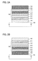
- FIGS. 2A and 2B each illustrate a stacked structure of the light-emitting element in Embodiment Mode 1.
- FIGS. 3A to 3C each illustrate a mode of light emission of the light-emitting element in Embodiment Mode 1.
- FIGS. 4A and 4B each illustrate a band structure of a light-emitting element in Embodiment Mode 2.
- FIGS. 5A and 5B each illustrate a stacked structure of the light-emitting element in Embodiment Mode 2.
- FIGS. 6A and 6B each illustrate a mode of a light emission of the light-emitting element in Embodiment Mode 2.
- FIG. 7 illustrates a band structure of the light-emitting element in Embodiment Mode 2.
- FIG. 8 illustrates a stacked structure of a light-emitting element in Embodiment Mode 3.
- FIGS. 9A and 9B illustrate an active matrix light-emitting device in Embodiment Mode 4.
- FIGS. 10A and 10B illustrate a passive matrix light-emitting device in Embodiment Mode 4.
- FIGS. 11A to 11D each illustrate an electronic appliance in Embodiment Mode 5.
- FIG. 12 illustrates a liquid crystal display device using a light-emitting device according to an aspect of the present invention as a backlight.
- FIG. 13 illustrates a table lamp using a light-emitting device according to an aspect of the present invention.
- FIG. 14 illustrates an indoor lighting apparatus using a light-emitting device according to an aspect of the present invention.
- FIGS. 15A and 15B each illustrate an element structure of a light-emitting element in Example 1.
- FIGS. 16A and 16B each illustrate an element structure of a light-emitting element in Example 2.
- FIG. 17 illustrates current density vs. luminance characteristics of light-emitting elements 1 to 4.
- FIG. 18 illustrates voltage vs. luminance characteristics of the light-emitting elements 1 to 4.
- FIG. 19 illustrates luminance vs. current efficiency characteristics of the light-emitting elements 1 to 4.
- FIG. 20 illustrates emission spectra of the light-emitting elements 1 to 3.
- FIG. 21 illustrates current density vs. luminance characteristics of light-emitting elements 5 to 8.
- FIG. 22 illustrates voltage vs. luminance characteristics of the light-emitting elements 5 to 8.
- FIG. 23 illustrates luminance vs. current efficiency characteristics of the light-emitting elements 5 to 8.
- FIG. 24 illustrates emission spectra of the light-emitting elements 5 to 7.
- FIG. 25 illustrates results of continuous lighting tests of the light-emitting elements 5 to 8 by constant current driving.
- FIG. 26 illustrates current density vs. luminance characteristics of light-emitting elements 9 to 12.
- FIG. 27 illustrates voltage vs. luminance characteristics of the light-emitting elements 9 to 12.
- FIG. 28 illustrates luminance vs. current efficiency characteristics of the light-emitting elements 9 to 12.
- FIG. 29 illustrates emission spectra of the light-emitting elements 9 to 11.
- FIG. 30 illustrates results of continuous lighting tests of the light-emitting elements 9 to 12 by constant current driving.
- FIG. 31 is a graph illustrating CV characteristics of YGASF.
- FIG. 32 is a graph illustrating CV characteristics of YGABP.
- FIG. 33 is a graph illustrating CV characteristics of TCTA.
- FIG. 34 is a graph illustrating CV characteristics of NPB.
- FIG. 35 is a graph illustrating CV characteristics of DNTPD.
- FIG. 36 is a graph illustrating CV characteristics of Alq.
- FIG. 37 is a graph illustrating CV characteristics of DPQd.
- FIG. 38 is a graph illustrating CV characteristics of 2PCAPA.
- Embodiment Mode 1 a light-emitting element of the present invention, which has a structure that reduces the rate of transport of holes that are carriers of the light-emitting element, is described.
- the light-emitting element in Embodiment Mode 1 includes a first electrode functioning as an anode, a second electrode functioning as a cathode, and an EL layer provided between the first electrode and the second electrode.
- the EL layer may be provided so that it includes at least a hole-injecting layer, a first hole-transporting layer, a second hole-transporting layer, and a light-emitting layer which are stacked in that order from the first electrode side, and that the highest occupied molecular orbital level (HOMO level) of the first hole-transporting layer is deeper (the absolute value is larger) or shallower (the absolute value is smaller) than the HOMO levels of the hole-injecting layer and the second hole-transporting layer.
- HOMO level highest occupied molecular orbital level
- the light-emitting element in Embodiment Mode 1 when voltage is applied to each electrode so that the potential of the first electrode 102 is higher than that of the second electrode 104
- an EL layer 103 includes, from the first electrode 102 side, a first layer (hole-injecting layer) 111 , a second layer (first hole-transporting layer) 112 , a third layer (second hole-transporting layer) 113 , a fourth layer (light-emitting layer) 114 , a fifth layer (electron-transporting layer) 115 , and a sixth layer (electron-injecting layer) 116 , as shown in FIGS. 1A and 1B .
- the EL layer 103 of the light-emitting element is provided so that the highest occupied molecular orbital level (HOMO level) of the second layer (first hole-transporting layer) 112 is deeper (the absolute value is larger) than the HOMO levels of the first layer (hole-injecting layer) and the third layer (second hole-transporting layer).
- the absolute value of the HOMO level of the second layer 112 is preferably larger than the HOMO levels of the first layer 111 and the third layer 113 by 0.1 eV or more.
- the EL layer 103 of the light-emitting element is provided so that the highest occupied molecular orbital level (HOMO level) of the second layer (first hole-transporting layer) 112 is shallower (the absolute value is smaller) than the HOMO levels of the first layer (hole-injecting layer) 111 and the third layer (second hole-transporting layer) 113 .
- the rate of transport of holes during the period from injection from the first electrode 102 to reach to the fourth layer (light-emitting layer) 114 can be reduced.
- the absolute value of the HOMO level of the second layer 112 is preferably smaller than the HOMO levels of the first layer 111 and the third layer 113 by 0.1 eV or more.
- FIG. 1A or 1B since the rate of transport of holes injected from the first electrode 102 can be reduced in either case of FIG. 1A or 1B , the carrier balance in the light-emitting element is improved, and higher efficiency of the element can be achieved. Further, which element structure of FIG. 1A or 1B is employed is determined depending on the HOMO levels of substances used for the first layer (hole-injecting layer) 111 , the second layer (first hole-transporting layer) 112 , and the third layer (second hole-transporting layer) 113 .
- the structure of the present invention is effective.
- the fourth layer (light-emitting layer) 114 contains a substance having an electron-transporting property
- an emission region is formed near the interface between the fourth layer (light-emitting layer) 114 and the third layer (second hole-transporting layer) 113 .
- cations serve as a quencher, whereby the emission efficiency decreases significantly.
- a structure of a light-emitting element in Embodiment Mode 1 is described using FIGS. 2A and 2B .
- a substrate 101 is used as a support of the light-emitting element.
- glass, quartz, plastics, or the like can be used, for example.
- the above substrate 101 may remain in a light-emitting device or an electronic appliance which is a product utilizing the light-emitting element of the present invention, but may only have a function of a support of the light-emitting element without remaining in an end product.
- a metal, an alloy, an electroconductive compound, a mixture thereof, or the like having a high work function is preferably used.
- a metal, an alloy, an electroconductive compound, a mixture thereof, or the like having a high work function (specifically, a work function of 4.0 eV or more) is preferably used.
- ITO Indium tin oxide
- IZO indium zinc oxide
- IWZO indium oxide containing tungsten oxide and zinc oxide
- gold Au
- platinum Pt
- nickel Ni
- tungsten W
- Cr chromium
- Mo molybdenum
- iron Fe
- Co cobalt
- Cu copper
- palladium Pd
- titanium Ti
- nitrides of metal materials e.g., titanium nitride
- Such materials are generally deposited by a sputtering method.
- indium zinc oxide (IZO) can be deposited by a sputtering method using a target in which 1 wt % to 20 wt % zinc oxide is added to indium oxide;
- indium oxide containing tungsten oxide and zinc oxide (IWZO) can be deposited by a sputtering method using a target in which 0.5 wt % to 5 wt % tungsten oxide and 0.1 wt % to 1 wt % zinc oxide are added to indium oxide.
- a sol-gel method or the like an inkjet method, a spin coating method, or the like may be used for the formation.
- any of a variety of metals, alloys, electroconductive compounds, and a mixture thereof can be used as a substance used for the first electrode 102 regardless of whether the work function is high or low.
- metals, alloys, electroconductive compounds, and a mixture thereof can be used as a substance used for the first electrode 102 regardless of whether the work function is high or low.
- aluminum (Al), silver (Ag), an alloy containing aluminum (AlSi), or the like can also be used.
- an element belonging to Group 1 or 2 of the periodic table which is a material having a low work function that is, an alkali metal such a lithium (Li) or cesium (Cs) or an alkaline-earth metal such as magnesium (Mg), calcium (Ca), or strontium (Sr); an alloy thereof (e.g., MgAg or AlLi); a rare earth metal such as europium (Eu) or ytterbium (Yb); an alloy thereof; or the like can also be used.
- the first electrode 102 is formed using an alkali metal, an alkaline-earth metal, or an alloy thereof, a vacuum evaporation method or a sputtering method can be used. Further alternatively, in the case of using a silver paste or the like, a coating method, an inkjet method, or the like can be used.
- the EL layer 103 formed over the first electrode 102 a known substance can be used, and any of low molecular compounds and high molecular compounds can be used. Note that the substance used to form the EL layer 103 includes not only a structure formed of only an organic compound but also a structure including an inorganic compound as a part.
- a hole-injecting layer that contains a substance having a high hole-injecting property a hole-transporting layer that contains a substance having a high hole-transporting property, a light-emitting layer that contains a light-emitting substance, an electron-transporting layer that contains a substance having a high electron-transporting property, an electron-injecting layer that contains a substance having a high electron-injecting property, and the like are combined with each other as appropriate and stacked.
- the EL layer 103 is needed to be provided so that it includes at least the hole-injecting layer, the first hole-transporting layer, the second hole-transporting layer, and the light-emitting layer which are stacked in that order from the first electrode 102 side, and that the highest occupied molecular orbital level (HOMO level) of the first hole-transporting layer is deeper (the absolute value is larger) than the HOMO levels of the hole-injecting layer and the second hole-transporting layer.
- HOMO level highest occupied molecular orbital level
- FIGS. 2A and 2B each illustrate the case where, from the first electrode 102 side, the first layer (hole-injecting layer) 111 , the second layer (first hole-transporting layer) 112 , the third layer (second hole-transporting layer) 113 , the fourth layer (light-emitting layer) 114 , the fifth layer (electron-transporting layer) 115 , and a sixth layer (electron-injecting layer) 116 are stacked in that order in a similar manner to FIGS. 1A and 1B .
- the first layer 111 which is the hole-injecting layer is a layer that contains a substance having a high hole-injecting property.
- a substance having a high hole-injecting property molybdenum oxide, vanadium oxide, ruthenium oxide, tungsten oxide, manganese oxide, or the like can be used.
- a phthalocyanine-based compound such as phthalocyanine (abbreviation: H 2 Pc), copper(II) phthalocyanine (abbreviation: CuPc), or vanadyl phthalocyanine (abbreviation: VOPc) can be used.
- aromatic amine compounds such as 4,4′,4′′-tris(N,N-diphenylamino)triphenylamine (abbreviation: TDATA), 4,4′,4′′-tris[N-(3-methylphenyl)-N-phenylamino]triphenylamine (abbreviation: MTDATA), 4,4′-bis[N-(4-diphenylaminophenyl)-N-phenylamino]biphenyl (abbreviation: DPAB), 4,4′-bis(N- ⁇ 4-[N-(3-methylphenyl)-N-phenylamino]phenyl ⁇ -N-phenylamino)biphenyl (abbreviation: DNTPD), 1,3,5-tris[N-(4-diphenylaminophenyl)-N-phenylamino]benzene (abbreviation: DPA3B), 3-[N-[N-(4-diphenylaminophenyl)
- a high molecular compound an oligomer, a dendrimer, a polymer, or the like
- high molecular compounds such as poly(N-vinylcarbazole) (abbreviation: PVK), poly(4-vinyltriphenylamine) (abbreviation: PVTPA), poly[N-(4- ⁇ N′-[4-(4-diphenyamin)phenyl]phenyl-N-phenylamino ⁇ phenyl)methacryla mide] (abbreviation: PTPDMA), and poly[N,N′-bis(4-butylphenyl)-N,N′-bis(phenyl)benzidine] (abbreviation: Poly-TPD).
- PVK poly(N-vinylcarbazole)
- PVTPA poly(4-vinyltriphenylamine)
- PTPDMA poly[N-(4- ⁇ N′-[4-(4-diphenyamin)phenyl]
- a high molecular compound to which acid is added such as poly(3,4-ethylenedioxythiophene)/poly(styrenesulfonic acid) (PEDOT/PSS), or polyaniline/poly(styrenesulfonic acid) (PAni/PSS), can be used.
- PEDOT/PSS poly(3,4-ethylenedioxythiophene)/poly(styrenesulfonic acid)
- PAni/PSS polyaniline/poly(styrenesulfonic acid)
- the composite material in which a substance having an acceptor property is contained in a substance having a high hole-transporting property can be used.
- a material used to form the electrode can be selected regardless of its work function. That is, for the first electrode 102 , a material with a low work function can also be used instead of a material with a high work function.
- Such a composite material can be formed by co-evaporation of a substance having a high hole-transporting property and an acceptor substance.
- composition refers to not only a state where two materials are simply mixed with each other but also a state where charge can be given and received between materials by mixture of a plurality of materials.
- organic compound used for the composite material any of a variety of compounds such as aromatic amine compounds, carbazole derivatives, aromatic hydrocarbons, and high molecular compounds (oligomers, dendrimers, polymers, and the like) can be used.
- the organic compound used for the composite material is preferably an organic compound having a high hole-transporting property. Specifically, a substance having a hole mobility of 10 6 cm 2 Ns or more is preferable. However, any substance other than the above substances may be used as long as it is a substance in which the hole-transporting property is higher than the electron-transporting property.
- organic compounds which can be used for the composite material are given in specific terms.
- organic compounds that can be used for the composite material there are aromatic amine compounds such as MTDATA, TDATA, DPAB, DNTPD, DPA3B, PCzPCA1, PCzPCA2, PCzPCN1, 4,4′-bis[N-(1-naphthyl)-N-phenylamino]biphenyl (abbreviation: NPB or ⁇ -NPD), and N,N′-bis(3-methylphenyl)-N,N′-diphenyl-[1,1′-biphenyl]-4,4′-diamine (abbreviation: TPD); carbazole derivatives such as 4,4′-di(N-carbazolyl)biphenyl (abbreviation: CBP), 1,3,5-tris[4-(N-carbazolyl)phenyl]benzene (abbreviation: TCPB), 9-[4-(N-carbazolyl)]phenyl-10-phenylan
- aromatic hydrocarbon compounds such as 2-tert-butyl-9,10-di(2-naphthyl)anthracene (abbreviation: t-BuDNA), 2-tert-butyl-9,10-di(1-naphthyl)anthracene, 9,10-bis(3,5-diphenylphenyl)anthracene (abbreviation: DPPA), 2-tert-butyl-9,10-bis(4-phenylphenyl)anthracene (abbreviation: t-BuDBA), 9,10-di(2-naphthyl)anthracene (abbreviation: DNA), 9,10-diphenylanthracene (abbreviation: DPAnth), 2-tert-butylanthracene (abbreviation: t-BuAnth), 9,10-bis(4-methyl-1-naphthyl)anthracene (abbreviation:
- an organic compound such as 7,7,8,8-tetracyano-2,3,5,6-tetrafluoroquinodimethane (abbreviation: F 4 -TCNQ) or chloranil, or a transition metal oxide
- F 4 -TCNQ 7,7,8,8-tetracyano-2,3,5,6-tetrafluoroquinodimethane
- chloranil or a transition metal oxide
- any of oxides of metals belonging to Groups 4 to 8 of the periodic table can be used.
- vanadium oxide, niobium oxide, tantalum oxide, chromium oxide, molybdenum oxide, tungsten oxide, manganese oxide, and rhenium oxide are preferable because of their high electron-accepting property.
- molybdenum oxide is particularly preferable because it is stable even in the atmosphere, has a low hygroscopic property, and is easy to handle.
- the composite material may be formed using the above high molecular compound such as PVK, PVTPA, PTPDMA, or Poly-TPD and the above substance having an acceptor property and then used for the first layer 111 .
- the second layer 112 which is the first hole-transporting layer and the third layer 113 which is the second hole-transporting layer contain substances each having a high hole-transporting property.
- the substance having a high hole-transporting property for example, it is possible to use any of the following low molecular organic compounds: aromatic amine compounds such as NPB (or ca-NPD), TPD, 4,4′-bis[N-(9,9′-dimethylfluoren-2-yl)-N-phenylamino]biphenyl (abbreviation: DFLDPBi), and 4,4′-bis[N-(spiro-9,9′-bifluoren-2-yl)-N-phenylamino]-1,1′-biphenyl (abbreviation: BSPB); 4,4′-di(N-carbazolyl)biphenyl (abbreviation: CBP); 2,7-di(N-carbazolyl)-spiro-9,9′-bi
- the above substances are mainly substances having a hole mobility of 10 ⁇ 6 cm 2 /Vs or more.
- any known substance other than the above substances may be used as long as it is a substance in which the hole-transporting property is higher than the electron-transporting property.
- Embodiment Mode 1 although the above substances can be used for forming the first layer 111 , the second layer 112 , and the third layer 113 , it is necessary to select substances to be used depending on the HOMO levels of the substances so that the highest occupied molecular orbital level (HOMO level) of the substance used for the second layer 112 is deeper (the absolute value is larger) or shallower (the absolute value is smaller) than the HOMO levels of the substances used for the first layer 111 and the third layer 113 .
- HOMO level highest occupied molecular orbital level
- the HOMO level of NPB is ⁇ 5.27 [eV]
- the HOMO level of YGASF is ⁇ 5.44 [eV]
- the HOMO level of YGABP is ⁇ 5.40 [eV]
- the HOMO level of TCTA is ⁇ 5.38 [eV]. Therefore, in the case of employing the structure shown in FIG.
- the HOMO level of NPB is ⁇ 5.27 [eV] and the HOMO level of DNTPD is ⁇ 5.06 [eV]. Therefore, in the case of employing the structure shown in FIG. 1B , a combination in which, for example, a composite material of NPB, the HOMO level of which is ⁇ 5.27, and molybdenum oxide is used for the first layer 111 , DNTPD, the HOMO level of which is ⁇ 5.06, is used for the second layer 112 , and NPB, the HOMO level of which is ⁇ 5.27, is used for the third layer 113 is possible.
- a band gap is formed by the first layer 111 , the second layer 112 , and the third layer 113 , and therefore the rate of transport of holes injected from the first electrode 102 can be suppressed.
- the amount of holes injected into the fourth layer 114 can be controlled.
- the fourth layer 114 is a light-emitting layer containing a substance having a high light-emitting property.
- any of low molecular organic compounds given below can be used.
- a light-emitting material which exhibits bluish light there are N,N′-bis[4-(9H-carbazol-9-yl)phenyl]-N,N-diphenylstilbene-4,4′-diamine (abbreviation: YGA2S), 4-(9H-carbazol-9-yl)-4′-(10-phenyl-9-anthryl)triphenylamine (abbreviation: YGAPA), and the like.
- N-(9,10-diphenyl-2-anthryl)-N,9-diphenyl-9H-carbazol-3-amine (abbreviation: 2PCAPA)
- N-[9,10-bis(1,1′-biphenyl-2-yl)-2-anthryl]-N,9-diphenyl-9H-carbazol-3-amine (abbreviation: 2PCABPhA)
- N-(9,10-diphenyl-2-anthryl)-N,N,N′-triphenyl-1,4-phenylenediamine abbreviation: 2DPAPA
- N-[9,10-bis(1,1′-biphenyl-2-yl)-2-anthryl]-N,N,′N′-tiphenyl-1,4-phenylenediamine (abbreviation: 2DPABPhA)
- BPT 5,12-bis(1,1′-biphenyl-4-yl)-6,11-diphenyltetracene
- N,N,N′,N′-tetrakis(4-methylphenyl)tetracene-5,11-diamine (abbreviation: p-mPhTD)
- p-mPhAFD 7,13-diphenyl-N,N,N′,N′-tetrakis(4-methylphenyl)acenaphtho[1,2-a]fluoranthene-3,10-diamine
- the fourth layer 114 may have a structure in which the above substance having a high light-emitting property is dispersed in another substance.
- the concentration of the substance to be dispersed is set to be preferably 20% or less of the total.
- a known substance can be used as a substance in which the substance having a light-emitting property is dispersed. It is preferable to use a substance having a lowest unoccupied molecular orbital level (LUMO level) deeper (the absolute value is larger) than that of the substance having a light-emitting property and a highest occupied molecular orbital level (HOMO level) shallower (the absolute value is smaller) than that of the substance having a light-emitting property.
- LUMO level lowest unoccupied molecular orbital level
- HOMO level highest occupied molecular orbital level
- a metal complex such as tris(8-quinolinolato)aluminum(III) (abbreviation: Alq), tris(4-methyl-8-quinolinolato)aluminum(III) (abbreviation: Almq 3 ), bis(10-hydroxybenzo[h]-quinolinato)beryllium(II) (abbreviation: BeBq 2 ), bis(2-methyl-8-quinolinolato)(4-phenylphenolato)aluminum(III) (abbreviation: BAlq), bis(8-quinolinolato)zinc(II) (abbreviation: Znq), bis[2-(2-benzoxazolyl)phenolato]zinc(II) (abbreviation: Zn(BOX) 2 ), or bis[2-(2-benzothiazolyl)phenolato]zinc(II) (abbreviation: Zn(BTZ) 2 ) can be used.
- Alq tri
- a heterocyclic compound such as 2-(4-biphenylyl)-5-(4-tert-butylphenyl)-1,3,4-oxadiazole (abbreviation: PBD), 1,3-bis[5-(p-tert-butylphenyl)-1,3,4-oxadiazol-2-yl]benzene (abbreviation: OXD-7), 3-(4-biphenylyl)-4-phenyl-5-(4-tert-butylphenyl)-1,2,4-triazole (abbreviation: TAZ), 2,2′,2′′-(1,3,5-benzenetriyl)-tris(1-phenyl-1H-benzimidazole) (abbreviation: TPBI), bathophenanthroline (abbreviation: BPhen), or bathocuproine (abbreviation: BCP) can be used.
- PBD 2-(4-biphenylyl)-5-(4-tert-
- a condensed aromatic compound such as 9-[4-(N-carbazolyl)]phenyl-10-phenylanthracene (abbreviation: CzPA), 3,6-diphenyl-9-[4-(10-phenyl-9-anthryl)phenyl]-9H-carbazole (abbreviation: DPCzPA), 9, 10-bis(3,5-diphenylphenyl)anthracene (abbreviation: DPPA), 9,10-di(2-naphthyl)anthracene (abbreviation: DNA), 2-tert-butyl-9,10-di(2-naphthyl)anthracene (abbreviation: t-BuDNA), 9,9′-bianthryl (abbreviation: BANT), 9,9′-(stilbene-3,3′-diyl)diphenanthrene (abbreviation: DPNS), 9,9′-(stilbene-4,4′-di
- a substance in which the substance having a light-emitting property is dispersed a plurality of kinds of substances can be used.
- a substance for suppressing crystallization such as rubrene
- NPB, Alq, or the like may be added in order to efficiently transfer energy to the substance having a light-emitting property.
- crystallization of the fourth layer 114 can be suppressed.
- concentration quenching caused by the high concentration of the substance having a light-emitting property can also be suppressed.
- a substance having an electron-transporting property is preferably used so that the substance having a light-emitting property is dispersed therein to form the fourth layer 114 .
- a high molecular compound given below can also be used.
- poly(9,9-dioctylfluorene-2,7-diyl) (abbreviation: POF)
- poly[(9,9-dioctylfluorene-2,7-diyl-co-(2,5-dimethoxybenzene-1,4-diyl)] (abbreviation: PF-DMOP)
- PPV poly(p-phenylenevinylene)
- PFBT poly[(9,9-dihexylfluorene-2,7-diyl)-alt-co-(benzo[2,1,3]thiadiazol-4,7-diyl)]
- PFBT poly[(9,9-dioctyl-2,7-divinylenefluorenylene)-alt-co-(2-methoxy-5-(2-ethylhexyloxy)-1,4-phenylene)]
- poly[2-methoxy-5-(2′-ethylhexoxy)-1,4-phenylenevinylene] (abbreviation: MEH-PPV), poly(3-butylthiophene-2,5-diyl), poly ⁇ [9,9-dihexyl-2,7-bis(1-cyanovinylene)fluorenylene]-alt-co-[2,5-bis(N,N-diphenyl amino)-1,4-phenylene] ⁇
- poly ⁇ [2-methoxy-5-(2-ethylhexyloxy)-1,4-bis(1-cyanovinylenephenylene)]-alt-co-[2,5-bis(N,N-diphenylamino)-1,4-phenylene] ⁇ (abbreviation: CN-PPV-DPD), and the like.
- the fifth layer 115 is an electron-transporting layer that contains a substance having a high electron-transporting property.
- a metal complex such as Alq, Almq 3 , BeBq 2 , BAlq, Znq, ZnPBO, or ZnBTZ, or the like can be used.
- a heterocyclic compound such as PBD, OXD-7, TAZ, TPBI, BPhen, or BCP can be used.
- the substances given here are mainly substances having an electron mobility of 10 6 cm 2 /Vs or more.
- the electron-transporting layer is not limited to a single layer but may have a stacked structure of two or more layers formed of the above substances.
- a high molecular compound can also be used.
- poly[(9,9-dihexylfluorene-2,7-diyl)-co-(pyridine-3,5-diyl)] (abbreviation: PF-Py)
- poly[(9,9-dioctyllfluorene-2,7-diyl)-co-(2,2′-bipyridine-6,6′-diyl)](abbreviation: PF-BPy), or the like can be used.
- the sixth layer 116 is an electron-injecting layer that contains a substance having a high electron-injecting property.
- a substance having a high electron-injecting property such as lithium fluoride (LiF), cesium fluoride (CsF), or calcium fluoride (CaF 2 ) can be used.
- a layer formed of a substance having an electron-transporting property which contains an alkali metal, an alkaline earth metal, or a compound thereof, specifically, a layer formed of Alq which contains magnesium (Mg), or the like may be used. Note that in this case, electrons can be more efficiently injected from the second electrode 104 .
- a metal, an alloy, an electroconductive compound, a mixture thereof, or the like having a low work function can be used.
- a metal, an alloy, an electroconductive compound, a mixture thereof, or the like having a low work function (specifically, a work function of 3.8 eV or less) can be used.
- cathode materials elements that belong to Group 1 and 2 of the periodic table, that is, alkali metals such as lithium (Li) and cesium (Cs), alkaline earth metals such as magnesium (Mg), calcium (Ca), and strontium (Sr), alloys containing them (MgAg or AILi), rare earth metals such as europium (Eu) and ytterbium (Yb), alloys containing them, and the like are given.
- the second electrode 104 is formed using an alkali metal, an alkaline-earth metal, or an alloy thereof
- a vacuum evaporation method or a sputtering method can be used.
- a coating method, an inkjet method, or the like can be used
- the second electrode 104 can be formed using any of a variety of conductive materials such as Al, Ag, ITO, and indium tin oxide containing silicon or silicon oxide regardless of whether the work function is high or low. These conductive materials can be deposited by a sputtering method, an inkjet method, a spin coating method, or the like.
- any of a variety of methods can be employed regardless of whether the method is a dry process or a wet process.
- a vacuum evaporation method, an inkjet method, a spin coating method, or the like can be used. It is to be noted a different formation method may be employed for each layer.
- the second electrode 104 can also be formed by a wet process such as a sol-gel method using a paste of a metal material instead of a dry process such as a sputtering method or a vacuum evaporation method or.
- the first electrode 102 and the second electrode 104 are an electrode having a light-transmitting property.
- first electrode 102 is an electrode having a light-transmitting property
- second electrode 104 is an electrode having a light-transmitting property
- light emitted from the EL layer 103 is extracted from the opposite side to the substrate 101 side through the second electrode 104 , as shown in FIG. 3B .
- first electrode 102 and the second electrode 104 are both electrodes having a light-transmitting property
- light emitted from the EL layer 103 is extracted to both the substrate 101 side and the opposite side, through the first electrode 102 and the second electrode 104 , as shown in FIG. 3C .
- the structure of the layers provided between the first electrode 102 and the second electrode 104 is not limited to the above structure.
- any structure other than the above structure may be used as long as it includes at least the first layer 111 which is the hole-injecting layer, the second layer 112 which is the first hole-transporting layer, the third layer 113 which is the second hole-transporting layer, and the fourth layer 114 which is the light-emitting layer, and substances are selected so that the highest occupied molecular orbital level (HOMO level) of the substance used for the second layer 112 is deeper (the absolute value is larger) or shallower (the absolute value is smaller) than the HOMO levels of the substances used for the first layer 111 and the third layer 113 .
- HOMO level highest occupied molecular orbital level
- a structure may be employed in which the second electrode 104 functioning as a cathode, the EL layer 103 , and the first electrode 102 functioning as an anode are stacked in that order over the substrate 101 .
- the EL layer 103 in this case has a structure in which the sixth layer 116 , the fifth layer 115 , the fourth layer 114 , the third layer 113 , the second layer 112 , and the first layer 111 are stacked in that order over the second electrode 104 .
- a passive matrix light-emitting device or an active matrix light-emitting device in which drive of the light-emitting element is controlled by a thin film transistor (TFT) can be manufactured.
- a staggered TFT or an inverted staggered TFT can be used as appropriate.
- a driver circuit formed over a TFT substrate may be formed of both of an n-type TFT and a p-type TFT or only either an n-type TFT or a p-type TFT.
- crystallinity of a semiconductor film used for the TFT An amorphous semiconductor film may be used, or a crystalline semiconductor film may be used.
- the band gap is formed by the first layer 111 , the second layer 112 , and the third layer 113 which are provided between the first electrode 102 and the fourth layer 114 which is the light-emitting layer, and therefore the rate of transport of holes injected from the first electrode 102 can be suppressed.
- the amount of holes injected into the fourth layer 114 can be controlled. Accordingly, the carrier balance of the whole light-emitting element can be improved, and an element having high efficiency can be formed.
- Embodiment Mode 2 a light-emitting element of the present invention, which has a structure that reduces the rate of transport of electrons in addition to the structure described in Embodiment Mode 1, which reduces the rate of transport of holes, is described.
- the light-emitting element in Embodiment Mode 2 includes a first electrode, a second electrode, and an EL layer provided between the first electrode and the second electrode.
- the EL layer may be provided so that it includes at least a hole-injecting layer, a first hole-transporting layer, a second hole-transporting layer, a light-emitting layer, and a carrier control layer which are stacked in that order from the first electrode side, and that the highest occupied molecular orbital level (HOMO level) of the first hole-transporting layer is deeper (the absolute value is larger) or shallower (the absolute value is smaller) than the HOMO levels of the hole-injecting layer and the second hole-transporting layer.
- HOMO level highest occupied molecular orbital level
- the EL layer 103 includes, from the first electrode 102 side, the first layer (hole-injecting layer) 111 , the second layer (first hole-transporting layer) 112 , the third layer (second hole-transporting layer) 113 , the fourth layer (light-emitting layer) 114 , a seventh layer 117 (a carrier control layer), the fifth layer (electron-transporting layer) 115 , and the sixth layer (electron-injecting layer) 116 , as shown in FIGS. 4A and 4B .
- the EL layer 103 of the light-emitting element is provided so that the highest occupied molecular orbital level (HOMO level) of the second layer (first hole-transporting layer) 112 is deeper (the absolute value is larger) than the HOMO levels of the first layer (hole-injecting layer) and the third layer (second hole-transporting layer).
- the absolute value of the HOMO level of the second layer 112 is preferably larger than the HOMO levels of the first layer 111 and the third layer 113 by 0.1 eV or more.
- the EL layer 103 of the light-emitting element is provided so that the highest occupied molecular orbital level (HOMO level) of the second layer (first hole-transporting layer) 112 is shallower (the absolute value is smaller) than the HOMO levels of the first layer (hole-injecting layer) 111 and the third layer (second hole-transporting layer) 113 .
- the rate of transport of holes during the period from injection from the first electrode 102 to reach to the fourth layer (light-emitting layer) 114 can be reduced.
- the absolute value of the HOMO level of the second layer 112 is smaller than the HOMO levels of the first layer 111 and the third layer 113 by 0.1 eV or more.
- the rate of transport of holes injected from the first electrode 102 can be reduced in either case of FIG. 4A or 4B .
- the rate of transport of electrons during the period from injection from the second electrode 104 to reach to the fourth layer (light-emitting layer) 114 can be reduced.
- which element structure of or FIGS. 4A and 4B is formed is determined depending on the HOMO levels of substances used for the first layer (hole-injecting layer) 111 , the second layer (first hole-transporting layer) 112 , and the third layer (second hole-transporting layer) 113 .
- the structure of the present invention is effective.
- the fourth layer (light-emitting layer) 114 contains a substance having an electron-transporting property
- an emission region is formed near the interface between the fourth layer (light-emitting layer) 114 and the third layer (second hole-transporting layer) 113 .
- cations serve as a quencher, whereby the emission efficiency decreases significantly.
- the first electrode 102 functions as an anode and the second electrode 104 functions as a cathode.
- the first electrode 102 functions as an anode and the second electrode 104 functions as a cathode.
- the second electrode 104 when voltage is applied to each electrode so that the potential of the first electrode 102 is higher than that of the second electrode 104 , light can be emitted.
- the substrate 101 is used as a support of the light-emitting element. Note that for the substrate 101 , glass, quartz, plastics, or the like can be used, for example.
- a metal, an alloy, an electroconductive compound, a mixture thereof, or the like having a high work function is preferably used, and a substance similar to those described in Embodiment Mode 1 can be used.
- the structure of the first layer (hole-injecting layer) 111 , the second layer (hole-transporting layer) 112 , the third layer (hole-transporting layer) 113 , and the fourth layer (light-emitting layer) 114 which are stacked in that order from the first electrode 102 side, and a formation method and a material which can be used for each layer are similar to those of Embodiment Mode 1. Therefore, description thereof is omitted in Embodiment Mode 2.
- Embodiment Mode 2 has a feature of providing, between the fourth layer (light-emitting layer) 114 and the second electrode 104 , the seventh layer (hereinafter, referred to as a carrier control layer) 117 that reduces the rate of transport of carriers (electrons); however, for the structure of the carrier control layer, two kinds of methods (a method for kinetically controlling the rate of transport of carriers and a method for thermodynamically controlling the rate of transport of carriers) can be used.
- a carrier control layer two kinds of methods (a method for kinetically controlling the rate of transport of carriers and a method for thermodynamically controlling the rate of transport of carriers) can be used.
- FIGS. 6A and 6B are conceptual diagrams thereof.
- the EL layer 103 is formed between the second electrode 104 and the second electrode 104 .
- the first layer (hole-injecting layer) 111 , the second layer (hole-transporting layer) 112 , the third layer (hole-transporting layer) 113 , the fourth layer (light-emitting layer) 114 , the seventh layer (carrier control layer) 117 , the fifth layer (electron-transporting layer) 115 , and the sixth layer (electron-injecting layer) 116 are formed in that order.
- the seventh layer (carrier control layer) 117 is formed of two or more kinds of organic compounds.
- a first organic compound 201 and a second organic compound 202 as shown in FIG. 6B .
- an organic compound having a high electron-transporting property an electron-transporting organic compound
- an organic compound having a high hole-transporting property a hole-transporting organic compound
- the organic compounds used for the second organic compound 202 and the first organic compound 201 have LUMO levels close to each other.
- a difference between the absolute value of the lowest unoccupied molecular orbital level (LUMO level) of the second organic compound 202 and the absolute value of the LUMO level of the first organic compound 201 is preferably 0.3 eV or less, more preferably 0.2 eV or less. That is, preferably, electrons that are carriers are easily transported between the first organic compound 201 and the second organic compound 202 .
- the second organic compound 202 since the second organic compound 202 has a LUMO level as close as that of the first organic compound 201 , electrons can be injected.
- the rate (v 1 ) of electron injection from the first organic compound 201 having an electron-transporting property into the second organic compound 202 having a hole-transporting property or the rate (v 2 ) of electron injection from the second organic compound 202 into the first organic compound 201 is smaller than the rate (v) of electron injection between the first organic compounds 201 .
- the rate of transport of electrons in the seventh layer 117 can be reduced compared to the case where the seventh layer 117 is formed of only the first organic compound 201 . That is, by forming the seventh layer 117 using the first organic compound 201 and the second organic compound 202 , the rate of transport of carriers (electrons) in the seventh layer 117 can be reduced.
- the concentration is preferably controlled so that the content of the second organic compound 202 is less than 50% of the total in mass ratio. Further preferably, the concentration is controlled so that the content of the second organic compound 202 is greater than or equal to 1 weight % and less than or equal to 20 weight % of the total.
- the first organic compound 201 contained in the seventh layer 117 specifically, there are metal complexes such as Alq, Almq 3 , BeBq 2 , BAlq, Znq, ZnPBO, and ZnBTZ; heterocyclic compounds such as PBD, OXD-7, TAZ, TPBI, BPhen, and BCP; and condensed aromatic compounds such as CzPA, DPCzPA, DPPA, DNA, t-BuDNA, BANT, DPNS, DPNS2, and TPB3.
- metal complexes such as Alq, Almq 3 , BeBq 2 , BAlq, Znq, ZnPBO, and ZnBTZ
- heterocyclic compounds such as PBD, OXD-7, TAZ, TPBI, BPhen, and BCP
- condensed aromatic compounds such as CzPA, DPCzPA, DPPA, DNA, t-BuDNA, BANT, DPNS, DPNS2, and TPB3.
- a high molecular compound such as poly[(9,9-dihexylfluorene-2,7-diyl)-co-(pyridine-3,5-diyl)](abbreviation: PF-Py) or poly[(9,9-dioctyllfluorene-2,7-diyl)-co-(2,2′-bipyridine-6,6′-diyl)] (abbreviation: PF-BPy) can be used.
- PF-Py poly[(9,9-dihexylfluorene-2,7-diyl)-co-(pyridine-3,5-diyl)]
- PF-BPy poly[(9,9-dioctyllfluorene-2,7-diyl)-co-(2,2′-bipyridine-6,6′-diyl)]
- a condensed aromatic hydrocarbon such as 9,10-diphenylanthracene (abbreviation: DPAnth) or 6,12-dimethoxy-5,11-diphenylchrysene; or an aromatic amine compound such as N,N-dipheyl-9-[4-(10-phenyl-9-anthryl)phenyl]-9H-carbazol-3-amine (abbreviation: CzAlPA), 4-(10-phenyl-9-anthryl)triphenylamine (abbreviation: DPhPA), N,9-diphenyl-N-[4-(10-phenyl-9-anthryl)phenyl]-9H-carbazol-3-amine (abbreviation: PCAPA), N,9-diphenyl-N- ⁇ 4-[4-(10-phenyl-9-anthryl)phenyl]phenyl ⁇ 9H-carbazol-3-amine (abbreviation: PCAPA), N,9-diphenyl-N-
- the above materials are combined with each other to form the seventh layer 117 , and accordingly transport of electrons from the first organic compound 201 to the second organic compound 202 or from the second organic compound 202 to the first organic compound 201 is suppressed so that the rate of transport of electrons of the seventh layer 117 can be suppressed.
- the seventh layer 117 has a structure in which the second organic compound 202 is dispersed in the first organic compound 201 , crystallization or aggregation over time is not easily caused.
- the above-described effect of suppressing electron transport does not easily change over time.
- the carrier balance does not easily change over time. This leads to an increase in the life of the light-emitting element, that is, improvement in reliability.
- a combination of a metal complex as the first organic compound 201 and an aromatic amine compound as the second organic compound 202 is preferable.
- a metal complex has a large dipole moment as well as a high electron-transporting property, whereas an aromatic amine compound has a relatively small dipole moment as well as a high hole-transporting property.
- the above-described effect of suppressing electron transport can be further increased.
- the dipole moment of the first organic compound 201 is P 1 and the dipole moment of the second organic compound 202 is P 2
- a combination satisfying P 1 /P 2 ⁇ 3 is preferable.
- the dipole moment of Alq that is a metal complex is 9.40 debye
- the dipole moment of 2PCAPA that is an aromatic amine compound is 1.15 debye. Accordingly, in the case where an organic compound having an electron-transporting property, such as a metal complex, is used as the first organic compound 201 and an organic compound having a hole-transporting property, such as an aromatic amine compound, is used as the second organic compound 202 , P 1 /P 2 ⁇ 3 is preferably satisfied.
- an emission color of the second organic compound contained in the seventh layer 117 and an emission color of the substance having a high light-emitting property which is contained in the fourth layer (light-emitting layer) 114 are preferably similar colors.
- a difference between the peak value of the emission spectrum of the second organic compound and the peak value of the emission spectrum of the substance having a high light-emitting property is preferably within 30 nm. The difference within 30 nm allows the emission color of the second organic compound and the emission color of the substance having a high light-emitting property to be similar colors. Therefore, if the second organic compound emits light due to a change in voltage or the like, a change in emission color can be suppressed.
- FIG. 7 is a conceptual diagram thereof (a band diagram).
- the EL layer 103 is included between the first electrode 102 and the second electrode 104 .
- the first layer (hole-injecting layer) 111 , the second layer (hole-transporting layer) 112 , the third layer (hole-transporting layer) 113 , the fourth layer (light-emitting layer) 114 , the seventh layer (carrier control layer) 117 , the fifth layer (electron-transporting layer) 115 , and the sixth layer (electron-injecting layer) 116 are formed in that order.
- the seventh layer (carrier control layer) 117 is formed of two or more kinds of organic compounds.
- the seventh layer (carrier control layer) 117 is formed of two kinds of organic compounds, a first organic compound and a second organic compound is described. Note that an organic compound having a high electron-transporting property (an electron-transporting organic compound) is used as the first organic compound and an organic compound having a function of trapping electrons (an electron-trapping organic compound) is used as the second organic compound.
- the organic compounds used as the first organic compound and the second organic compound have LUMO levels that are greatly different from each other.
- the absolute value of the lowest unoccupied molecular orbital level (LUMO level) of the second organic compound is preferably larger than the absolute value of the LUMO level of the first organic compound by 0.3 eV or more.
- a hole is injected from the first electrode 102 into the fourth layer (light-emitting layer) 114 through the first layer 111 , the second layer 112 , and the third layer 113 .
- an electron is injected from the second electrode 104 into the seventh layer (carrier control layer) 117 through the sixth layer 116 and the fifth layer 115 . Since the seventh layer 117 is formed of the first organic compound having an electron-transporting property and the second organic compound having an electron-trapping property, an electron injected into the seventh layer 117 enters the LUMO level of the second organic compound, not that of the first organic compound. Accordingly, the rate of transport of electrons can be reduced.
- the rate of transport of electrons in the seventh layer 117 can be reduced compared to the case where the seventh layer 117 is formed of only the first organic compound. That is, by forming the seventh layer 117 using the first organic compound and the second organic compound, rate of transport of carriers (electrons) in the seventh layer 117 can be reduced.
- the concentration is controlled so that the content of the second organic compound is preferably less than 50% of the total in mass ratio. Further preferably, the concentration is controlled so that the content of the second organic compound is greater than or equal to 0.1 weight % and less than or equal to 5 weight % of the total.
- a metal complex such as Alq, Almq 3 , BeBq 2 , BAlq, Znq, ZnPBO, or ZnBTZ; a heterocyclic compound such as PBD, OXD-7, TAZ, TPBI, BPhen, or BCP; or a condensed aromatic compound such as CzPA, DPCzPA, DPPA, DNA, t-BuDNA, BANT, DPNS, DPNS2, or TPB3 can be used.
- a metal complex such as Alq, Almq 3 , BeBq 2 , BAlq, Znq, ZnPBO, or ZnBTZ
- a heterocyclic compound such as PBD, OXD-7, TAZ, TPBI, BPhen, or BCP
- a condensed aromatic compound such as CzPA, DPCzPA, DPPA, DNA, t-BuDNA, BANT, DPNS, DPNS2, or TPB3
- a high molecular compound such as poly[(9,9-dihexylfluorene-2,7-diyl)-co-(pyridine-3,5-diyl)] (abbreviation: PF-Py) or poly[(9,9-dioctyllfluorene-2,7-diyl)-co-(2,2′-bipyridine-6,6′-diyl)] (abbreviation: PF-BPy) can be used.
- PF-Py poly[(9,9-dioctyllfluorene-2,7-diyl)-co-(2,2′-bipyridine-6,6′-diyl)]
- PF-BPy poly[(9,9-dioctyllfluorene-2,7-diyl)-co-(2,2′-bipyridine-6,6′-diyl)]
- the second organic compound contained in the seventh layer 117 any of substances given below can be used. Note that although the second organic compound itself may emit light, in that case, the emission color of the fourth layer (light-emitting layer) 114 and the emission color of the second organic compound are preferably similar colors in order to keep the color purity of the light-emitting element.
- the second organic compound is preferably a compound which exhibits emission in the range of blue to blue green light, such as acridone, coumarin 102, coumarin 6H, coumarin 480D, or coumarin 30.
- the organic compound contained in the fourth layer (light-emitting layer) 114 is an organic compound that exhibits greenish light emission, such as 2PCAPA, 2PCABPhA, 2DPAPA, 2DPABPhA, 2YGABPhA, or DPhAPhA
- the second organic compound is preferably a compound that exhibits light emission in the range of bluish green to yellowish green, such as N,N-dimethyluinacridone (abbreviation: DMQd), N,N-diphenylquinacridone (abbreviation: DPQd), 9,18-dihydrobenzo[h]benzo[7,8]quino[2,3-b]acridine-7,16-dione (abbreviation: DMNQd-1), 9,18-dihydro-9,18-dimethylbenzo[h]benzo[7,8]quino[2,3-b]acridine-7,16-dione (abbreviation: DMNQd-2
- the organic compound contained in the fourth layer (light-emitting layer) 114 is an organic compound which exhibits yellowish light emission, such as rubrene or BPT
- the second organic compound is preferably a substance which exhibits light emission in the range of yellowish green to golden yellow, such as DMQd or (2- ⁇ 2-[4-(9H-carbazol-9-yl)phenyl]ethenyl ⁇ -6-methyl-4H-pyran-4-ylidene)propanedinitrile (abbreviation: DCMCz).
- the organic compound contained in the fourth layer (light-emitting layer) 114 is an organic compound which exhibits reddish light emission, such as p-mPhTD or p-mPhAFD
- the second organic compound is preferably a substance which exhibits light emission in the range of orange to red, such as 2- ⁇ 2-[4-(dimethylamino)phenyl]ethenyl ⁇ -6-methyl-4H-pyran-4-ylidene)propanedinitrile (abbreviation: DCM1), ⁇ 2-methyl-6-[2-(2,3,6,7-tetrahydro-1H,5H-benzo[ ]quinolizin-9-yl)ethenyl]-4H-pyran-4-ylidene ⁇ propanedinitrile (abbreviation: DCM2), ⁇ 2-(1,1-dimethylethyl)-6-[2-(2,3,6,7-tetrahydro-1,1,7,7-tetramethyl-1H,5H-benzo
- the second organic compound is preferably also a phosphorescent compound.
- the second organic compound may be a red phosphorescent compound such as (acetylacetonato)bis[2,3-bis(4-fluorophenyl)quinoxalinato]iridium(II) (abbreviation: Ir(Fdpq) 2 (acac)).
- Ir(Fdpq) 2 abbreviation: Ir(Fdpq) 2 (acac)
- a quinacridone derivative such as DMQd, DPQd, DMNQd-1, or DMNQd-2 is chemically stable and thus preferably used. That is, by applying a quinacridone derivative, the life of the light-emitting element can be particularly extended. Further, since a quinacridone derivative exhibits greenish light emission, the element structure of the light-emitting element of the present invention is particularly effective for a greenish light-emitting element. Since green is a color that needs the highest luminance in manufacturing a full-color display, a greenish light-emitting element deteriorates faster than light-emitting elements of other colors in some cases. However, such a problem can be suppressed by applying the invention.
- the absolute value of the LUMO level of the second organic compound is preferably larger than the absolute value of the LUMO level of the first organic compound by 0.3 eV or more. Therefore, the first organic compound may be selected as appropriate so as to satisfy the above-described condition depending on the kind of the substance used for the second organic compound.
- the emission color of the substance having a high light-emitting property contained in the fourth layer 114 and the emission color of the second organic compound contained in the seventh layer 117 are preferably similar colors.
- a difference between the peak value of the emission spectrum of the substance having a high light-emitting property and the peak value of the emission spectrum of the second organic compound is preferably within 30 nm. The difference within 30 nm allows the emission color of the substance having a high light-emitting property and the emission color of the second organic compound to be similar colors. Therefore, if the second organic compound emits light due to a change in voltage or the like, a change in emission color can be suppressed.
- the second organic compound does not necessarily emit light.
- the concentration of the second organic compound in the seventh layer 117 so that only light emission of the substance having a high light-emitting property can be obtained (to set the concentration of the second organic compound to be slightly lower than that of the substance having a high light-emitting property so that light emission of the second organic compound can be suppressed).
- the emission color of the substance having a high light-emitting property and the emission color of the second organic compound are similar colors (i.e., they have substantially the same levels of energy gaps). Therefore, energy is not easily transferred from the substance having a high light-emitting property to the second organic compound, and thus high emission efficiency can be achieved.
- the second organic compound is preferably a coumarin derivative such as coumarin 102, coumarin 6H, coumarin 480D, coumarin 30, coumarin 6, coumarin 545T, or coumarin 153.
- a coumarin derivative has a relatively low electron-trapping property, the concentration of the coumarin derivative added to the first organic compound may be relatively high. That is, the concentration can be easily controlled, and a layer having desired properties for controlling transport of carriers can be formed. Further, since a coumarin derivative has high emission efficiency, a decrease in efficiency of the whole light-emitting element can be suppressed even if the second organic compound emits light.
- the seventh layer 117 in the present invention can be formed by the above-described two kinds of methods (a method for kinetically controlling transport of carriers and a method for thermodynamically controlling transport of carriers), and the thickness of the seventh layer 117 is preferably greater than or equal to 5 nm and less than or equal to 20 nm in either structure. This is because if the thickness is larger, an excessive decrease in rate of transport of electrons leads to an increase in driving voltage, whereas if the thickness is smaller, a function of controlling carrier transport could be impaired.
- the seventh layer 117 in the present invention is a layer for controlling the rate of transport of electrons
- the seventh layer 117 may be formed between the second electrode 104 and the fourth layer (light-emitting layer) 114 . More preferably, the seventh layer 117 is formed in contact with the fourth layer (light-emitting layer) 114 .
- injection of electrons into the fourth layer (light-emitting layer) 114 can be directly controlled; thus, a change in carrier balance in the fourth layer (light-emitting layer) 114 over time can be further suppressed, and a large effect can be obtained in terms of improvement in element life.
- the first organic compound contained in the seventh layer 117 and the organic compound which is contained in the fourth layer (light-emitting layer) 114 in large amounts are preferably different organic compounds.
- the fourth layer (light-emitting layer) 114 contains a compound (a third organic compound) in which a substance having a high light-emitting property is dispersed and the substance having a high light-emitting property (a fourth organic compound)
- the third organic compound and the first organic compound are preferably different organic compounds.
- the transport of carriers (electrons) from the seventh layer 117 to the fourth layer (light-emitting layer) 114 is suppressed also between the first organic compound and the third organic compound, and the effect obtained by the provision of the seventh layer 117 can be further enhanced.
- the carrier balance can be precisely controlled by controlling a combination of substances, the mixture ratio thereof, the thickness of the layer, or the like.
- the carrier balance can be controlled more easily than in the conventional manner.
- transport of carriers is controlled using the organic compound, the mixture ratio of which is smaller in the seventh layer 117 , the carrier balance does not easily change compared to the case of control using one substance. Accordingly, a light-emitting element which does not easily change over time and has a long life can be realized.
- the fifth layer (electron-transporting layer) 115 and the sixth layer (electron-injecting layer) 116 are stacked in that order over the above-described seventh layer (carrier control layer) 117 , the structure thereof, a formation method, and a material that can be used for each layer are similar to those of Embodiment Mode 1. Therefore, description thereof is omitted in Embodiment Mode 2.
- the second electrode 104 is formed over the sixth layer (electron-injecting layer) 116 .
- a formation method and a material that can be used for the second electrode 104 are also similar to those of Embodiment Mode 1. Therefore, the description thereof is omitted in Embodiment Mode 2.
- Embodiment Mode 2 when only the first electrode 102 is an electrode having a light-transmitting property, light emitted from the EL layer 103 is extracted from the substrate 101 side through the first electrode 102 , as shown in FIG. 3A .
- the second electrode 104 is an electrode having a light-transmitting property, light emitted from the EL layer 103 is extracted from the opposite side to the substrate 101 side through the second electrode 104 , as shown in FIG. 3B .
- first electrode 102 and the second electrode 104 are both electrodes having a light-transmitting property
- light emitted from the EL layer 103 is extracted to both the substrate 101 side and the opposite side, through the first electrode 102 and the second electrode 104 , as shown in FIG. 3C .
- the structure of the layers provided between the first electrode 102 and the second electrode 104 is not limited to the above structure.
- any structure other than the above structure may be used as long as it includes at least the first layer 111 which is the hole-injecting layer, the second layer 112 which is the first hole-transporting layer, the third layer 113 which is the second hole-transporting layer, the fourth layer 114 which is the light-emitting layer, and the seventh layer 117 which is the carrier control layer, and substances are selected so that the highest occupied molecular orbital level (HOMO level) of the substance used for the second layer 112 is deeper (the absolute value is larger) or shallower (the absolute value is smaller) than the HOMO levels of the substances used for the first layer 111 and the third layer 113 .
- HOMO level highest occupied molecular orbital level
- the second cathode 104 functioning as a cathode, the EL layer 103 , and the first electrode 102 functioning as an anode are stacked in that order over the substrate 101
- the EL layer 103 in this case has a structure in which the sixth layer 116 , the fifth layer 115 , the seventh layer 117 , the fourth layer 114 , the third layer 113 , the second layer 112 , and the first layer 111 are stacked in that order over the second electrode 104 .
- a passive matrix light-emitting device or an active matrix light-emitting device in which drive of the light-emitting element is controlled by a thin film transistor (TFT) can be manufactured.
- a staggered TFT or an inverted staggered TFT can be used as appropriate.
- a driver circuit formed over a TFT substrate may be formed of both of an n-type TFT and a p-type TFT or only either an n-type TFT or a p-type TFT.
- crystallinity of a semiconductor film used for the TFT An amorphous semiconductor film may be used, or a crystalline semiconductor film may be used.
- the band gap is formed by the first layer 111 , the second layer 112 , and the third layer 113 which are provided between the first electrode 102 and the fourth layer 114 which is the light-emitting layer, and therefore the rate of transport of holes injected from the first electrode 102 can be suppressed. Accordingly, since generation of cations in the vicinity of the fourth layer (light-emitting layer) 114 can be suppressed, a decrease in emission efficiency can be suppressed. Thus, the carrier balance can be improved, and an element having high efficiency can be formed.
- the seventh layer 117 is provided between the second electrode 104 and the fourth layer (light-emitting layer) 114 to reduce the rate of transport of carriers (electrons); accordingly, an emission region, which has been so far formed near the interface between the fourth layer (light-emitting layer) 114 and the third layer (hole-transporting layer) 113 because of the fast transport rate, can be formed more centrally in the fourth layer (light-emitting layer) 114 than in the conventional manner.
- the seventh layer 117 is provided to reduce the rate of transport of carriers (electrons); accordingly, it is possible to prevent deterioration of the third layer (hole-transporting layer) 113 , which is caused by carriers (electrons) which reach, from the fourth layer (light-emitting layer) 114 , the third layer (hole-transporting layer) 113 without contributing to light emission. Furthermore, by reducing the rate of transport of carriers (electrons), it is possible not only to control the amount of carriers (electrons) injected into the fourth layer (light-emitting layer) 114 but also to inhibit the controlled amount of carriers (electrons) from changing over time. Thus, since a decrease in the probability of recombination by deterioration of the balance over time can be prevented, improvement in element life (suppression of deterioration of luminance over time) can also be achieved.
- the rate of transport of holes and electrons which are injected into the fourth layer 114 is controlled so as to be reduced, the carrier balance in the fourth layer 114 improves and the probability of the recombination increases; therefore, the emission efficiency can be improved.
- Embodiment Mode 2 can be combined with any of the structures described in Embodiment Mode 1, as appropriate.
- Embodiment Mode 3 a light-emitting element having a plurality of EL layers of the light-emitting elements described in Embodiment Mode 1 and 2 (hereinafter, referred to as a stacked-type element) is described using FIG. 8 .
- This light-emitting element is a stacked-type light-emitting element that has a plurality of EL layers (a first EL layer 803 and a second EL layer 804 ) between a first electrode 801 and a second electrode 802 .
- a structure of two EL layers is described in Embodiment Mode 3, a structure of three or more EL layers may be employed.
- the first electrode 801 functions as an anode and the second electrode 802 functions as a cathode.
- the first electrode 801 and the second electrode 802 can be made to have structures similar to those described in Embodiment Mode 1.
- structures similar to those described in Embodiment Mode 1 and 2 can be used.
- structures of the first EL layer 803 and the second EL layer 804 may be the same or different from each other and can be similar to those described in Embodiment Mode 1 or 2.
- a charge generation layer 805 is provided between the plurality of EL layers (the first EL layer 803 and the second EL layer 804 ).
- the charge generation layer 805 has a function of injecting electrons into one of the EL layers and injecting holes into the other of the EL layers when voltage is applied to the first electrode 801 and the second electrode 802 .
- the charge generation layer 805 injects electrons into the first EL layer 803 and injects holes into the second EL layer 804 .
- the charge generation layer 805 preferably has a light-transmitting property in terms of light extraction efficiency. Further, the charge generation layer 805 functions even when it has lower conductivity than the first electrode 801 and the second electrode 802 .
- the charge generation layer 805 may have either a structure in which an acceptor substance is added to a substance having a high hole-transporting property or a structure in which a donor substance is added to a substance having a high electron-transporting property. Alternatively, both of these structures may be stacked.
- an aromatic amine compound such as 4,4′-bis[N-(1-naphthyl)-N-phenylamino]biphenyl (abbreviation: NPB or ⁇ -NPD), N,N′-bis(3-methylphenyl)-N,N′-diphenyl-[1,1′-biphenyl]-4,4′-diamine (abbreviation: TPD), 4,4′,4′′-tris(N,N-diphenylamino)triphenylamine (abbreviation: TDATA), 4,4′,4′′-tris[N-(3-methylphenyl)-N-phenylamino]triphenylamine (abbreviation: MTDATA), or 4,4′-bis[N-(spiro-9,9′-bifluoren-2-yl
- NPB or ⁇ -NPD N,N′-bis(3-methylphenyl)-N,N′-diphenyl-[1,1′-
- the substances given here mainly are substances having a hole mobility of 10 ⁇ 6 cm 2 /(V ⁇ s) or more.
- any substance other than the above substances may be used as long as it is a substance in which the hole-transporting property is higher than the electron-transporting property.
- F 4 -TCNQ 7,7,8,8-tetracyano-2,3,5,6-tetrafluoroquinodimethane
- chloranil and the like
- a transition metal oxide can be given.
- oxides of metals that belong to Group 4 to Group 8 in the periodic table can be given.
- vanadium oxide, niobium oxide, tantalum oxide, chromium oxide, molybdenum oxide, tungsten oxide, manganese oxide, and rhenium oxide are preferable since their electron-accepting properties are high.
- molybdenum oxide is particularly preferable because it is stable even in the atmosphere, has a low hygroscopic property, and is easy to handle.
- a metal complex having a quinoline skeleton or a benzoquinoline skeleton such as tris(8-quinolinolato)aluminum (abbreviation: Alq), tris(4-methyl-8-quinolinolato)aluminum (abbreviation: Almq 3 ), bis(10-hydroxybenzo[h]-quinolinato)beryllium (abbreviation: BeBq 2 ), or bis(2-methyl-8-quinolinolato)(4-phenylphenolato)aluminum (abbreviation: BAlq), or the like can be used.
- Alq tris(8-quinolinolato)aluminum
- Almq 3 tris(4-methyl-8-quinolinolato)aluminum
- BeBq 2 bis(10-hydroxybenzo[h]-quinolinato)beryllium
- BAlq bis(2-methyl-8-quinolinolato)(4-phenylphenolato
- a metal complex having an oxazole-based or thiazole-based ligand such as bis[2-(2-benzoxazolyl)phenolato]zinc(II) (abbreviation: Zn(BOX) 2 ), or bis[2-(2-benzothiazolyl)phenolato]zinc(II) (abbreviation: Zn(BTZ) 2 ), or the like can be used.
- 2-(4-biphenylyl)-5-(4-tert-butylphenyl)-1,3,4-oxadiazole abbreviation: PBD
- 1,3-bis[5-(p-tert-butylphenyl)-1,3,4-oxadiazol-2-yl]benzene abbreviation: OXD-7
- 3-(4-biphenylyl)-4-phenyl-5-(4-tert-butylphenyl)-1,2,4-triazole abbreviation: TAZ
- bathophenanthroline abbreviation: BPhen
- bathocuproine abbreviation: BCP
- the materials given here are mainly materials having an electron mobility of 10 ⁇ 6 cm 2 /(V ⁇ s) or more.
- any substance other than the above substances may be used as long as it is a substance in which the electron-transporting property is higher than the hole-transporting property.
- an alkali metal, an alkaline earth metal, a rare earth metal, a metal that belongs to Group 13 of the periodic table, or an oxide or carbonate thereof can be used.
- lithium (Li), cesium (Cs), magnesium (Mg), calcium (Ca), ytterbium (Yb), indium (In), lithium oxide, cesium carbonate, or the like is preferably used.
- an organic compound such as tetrathianaphthacene may be used for the donor material.
- the present invention can be similarly applied to a light-emitting element in which three or more EL layers are stacked.
- a plurality of EL layers to be partitioned from each other with a charge generation layer between a pair of electrodes, like the light-emitting element according to Embodiment Mode 3, emission from a region of high luminance can be realized at a low current density, and thus an element with a long life can be achieved.
- a drop in voltage due to the resistance of an electrode material can be suppressed, and thus uniform emission in a large area can be achieved.
- a light-emitting device which can be driven at low voltage and has low power consumption can be realized.
- a desired emission color can be obtained from the whole light-emitting element.
- the light-emitting element having two EL layers when an emission color of the first EL layer and an emission color of the second EL layer are made to be complementary colors, it is possible to obtain a light-emitting element from which white light is emitted from the whole light-emitting element.
- the complementary colors refer to colors that can produce an achromatic color when they are mixed. That is, white light emission can be obtained by mixture of light from substances whose emission colors are complementary colors.
- white light can be similarly obtained from the whole light-emitting element when an emission color of a first EL layer is red, an emission color of a second EL layer is green, and an emission color of a third EL layer is blue.
- Embodiment Mode 3 can be combined with any of the structures described in Embodiment Modes 1 and 2, as appropriate.
- FIGS. 9A and 9B a light-emitting device having a light-emitting element of the present invention in a pixel portion is described using FIGS. 9A and 9B .
- FIG. 9A is a top view showing the light-emitting device
- FIG. 9B is a cross-sectional view taken along lines A-A′ and B-B′ of FIG. 9A .
- a portion 901 is a driver circuit portion (a source side driver circuit); a portion 902 , indicated by a dotted line, is a pixel portion; and a portion 903 , indicated by a dotted line, is a driver circuit portion (a gate side driver circuit).
- a portion 904 is a sealing substrate; a portion 905 is a sealant; and a portion enclosed by the sealant 905 is a space 907 .
- a leading wiring 908 is a wiring for transmitting signals to be input to the source side driver circuit 901 and the gate side driver circuit 903 and receives signals such as a video signal, a clock signal, a start signal, and a reset signal from a flexible printed circuit (FPC) 909 that is to be an external input terminal.
- FPC flexible printed circuit
- the FPC may be provided with a printed wiring board (PWB).
- PWB printed wiring board
- the light-emitting device in this specification includes not only a light-emitting device itself but also a light-emitting device attached with an FPC or a PWB.
- each driver circuit portion may be any of a variety of circuits such as a CMOS circuit, a PMOS circuit, and an NMOS circuit.
- a driver-integrated type structure in which a driver circuit is formed over a substrate is described, a driver circuit is not necessarily formed over a substrate but can be formed externally from a substrate.
- the pixel portion 902 is formed of a plurality of pixels each including a switching TFT 911 , a current control TFT 912 , and a first electrode 913 which is electrically connected to a drain of the current control TFT 912 .
- an insulator 914 is formed to cover an end portion of the first electrode 913 .
- the insulator 914 is desirably formed so as to have a curved surface with curvature at an upper end portion or a lower end portion thereof in order to make the coverage be favorable.
- the insulator 914 can be formed to have a curved surface with a curvature radius (greater than or equal to 0.2 ⁇ m and less than or equal to 3 m) only at the upper end portion.
- a negative type material becomes insoluble in an etchant by light irradiation
- a positive type material which becomes soluble in an etchant by light irradiation can be used as the insulator 914 .
- An EL layer 916 and a second electrode 917 are formed over the first electrode 913 .
- a material used for the first electrode 913 any of a variety of metals, alloys, and electroconductive compounds, or a mixture thereof can be used.
- the first electrode 913 is used as an anode, it is preferable to use, among these materials, any of metals, alloys, and electroconductive compounds, a mixture thereof, or the like having a high work function (a work function of 4.0 eV or more).
- a stacked structure is employed, resistance as a wiring is low, a good ohmic contact is formed, and further the first electrode 913 can be made to function as an anode.
- the EL layer 916 is formed by any of a variety of methods such as an evaporation method using an evaporation mask, an inkjet method, and a spin coating method.
- the EL layer 916 has the structure described in Embodiment Mode 1 or 2.
- a material used for the EL layer 916 a low molecular compound or a high molecular compound (including an oligomer and a dendrimer) may be used.
- the material used for the EL layer not only an organic compound but also an inorganic compound may be used.
- any of a variety of metals, alloys, and electroconductive compounds, or a mixture thereof can be used.
- the second electrode 917 is used as a cathode, it is preferable to use, among these materials, any of metals, alloys, and electroconductive compounds, a mixture thereof, or the like having a low work function (a work function of 3.8 eV or less).
- a work function of 3.8 eV or less a work function of 3.8 eV or less.
- alkali metals such as lithium (Li) and cesium (Cs)
- alkaline earth metals such as magnesium (Mg), calcium (Ca), and strontium (Sr); alloys thereof (MgAg or AlLi); and the like are given.
- a stack of a metal thin film with a reduced thickness and a transparent conductive film indium tin oxide (ITO), indium tin oxide containing silicon or silicon oxide, indium zinc oxide (IZO), or indium oxide containing tungsten oxide and zinc oxide (IWZO) can also be used.
- ITO indium tin oxide
- IZO indium tin oxide containing silicon or silicon oxide
- IWZO indium oxide containing tungsten oxide and zinc oxide
- the sealing substrate 904 is attached using the sealant 905 to the element substrate 910 so that the light-emitting element 918 is provided in the space 907 surrounded by the element substrate 910 , the sealing substrate 904 , and the sealant 905 .
- the space 907 is filled with a filler.
- the space 907 is filled with an inert gas (nitrogen, argon, or the like), and where the space 907 may be filled with the sealant 905 .
- an epoxy-based resin is preferably used for the sealant 905 . Further, it is preferable that these materials hardly transmit water or oxygen. Further, as the sealing substrate 904 , instead of a glass substrate or a quartz substrate, a plastic substrate formed of fiberglass-reinforced plastic (FRP), polyvinyl fluoride (PVF), polyester, acrylic, or the like can be used.
- FRP fiberglass-reinforced plastic
- PVF polyvinyl fluoride
- polyester acrylic, or the like
- an active matrix light-emitting device having the light-emitting element of the present invention can be obtained.
- FIGS. 10A and 10B are a perspective view and a cross-sectional view of a passive matrix light-emitting device using the light-emitting element of the present invention. Note that FIG. 10A is a perspective view of the light-emitting device and FIG. 10B is a cross-sectional view taken along a line X-Y of FIG. 10A .
- an EL layer 1004 is provided between a first electrode 1002 and a second electrode 1003 over a substrate 1001 .
- An end portion of the first electrode 1002 is covered by an insulating layer 1005 .
- a partition layer 1006 is provided over the insulating layer 1005 . Sidewalls of the partition layer 1006 have a slant such that a distance between one sidewall and the other sidewall becomes narrower as the sidewalls gets closer to a surface of the substrate.
- a cross section taken in the direction of a shorter side of the partition layer 1006 has a trapezoidal shape, and the base of the trapezoid (a side of the trapezoid which is parallel to the surface of the insulating layer 1005 and is in contact with the insulating layer 1005 ) is shorter than the upper side of the trapezoid (a side of the trapezoid which is parallel to the surface of the insulating layer 1005 and is not in contact with the insulating layer 1005 ).
- the provision of the partition layer 1006 in this manner can prevent the light-emitting element from being defective due to static electricity or the like.
- the passive matrix light-emitting device using the light-emitting element of the present invention can be obtained.
- any of the light-emitting devices described in this embodiment mode are formed using the light-emitting element of the present invention, which has high emission efficiency, and accordingly a light-emitting device having reduced power consumption can be obtained.
- Embodiment Mode 4 can be combined with any of the structures described in Embodiment Modes 1 to 3, as appropriate.
- an electronic appliance including, as a part thereof, the light-emitting device of the present invention, which is described in Embodiment Mode 4, is described.
- the electronic appliance include cameras such as video cameras or digital cameras, goggle type displays, navigation systems, audio playback devices (e.g., car audio systems and audio systems), computers, game machines, portable information terminals (e.g., mobile computers, cellular phones, portable game machines, and electronic books), image playback devices in which a recording medium is provided (specifically, devices that are capable of playing back recording media such as digital versatile discs (DVDs) and equipped with a display unit that can display images), and the like.
- Specific examples of these electronic appliances are shown in FIGS. 11A to 11D .
- FIG. 11A shows a television set according to the present invention, which includes a housing 9101 , a support base 9102 , a display portion 9103 , a speaker portion 9104 , a video input terminal 9105 , and the like.
- the light-emitting device of the present invention can be applied to the display portion 9103 . Since the light-emitting device of the present invention has a feature of high emission efficiency, a television set having reduced power consumption can be obtained by applying the light-emitting device of the present invention.
- FIG. 11B shows a computer according to the present invention, which includes a main body 9201 , a housing 9202 , a display portion 9203 , a keyboard 9204 , an external connection port 9205 , a pointing device 9206 , and the like.
- the light-emitting device of the present invention can be applied to the display portion 9203 . Since the light-emitting device of the present invention has a feature of high emission efficiency, a computer having reduced power consumption can be obtained by applying the light-emitting device of the present invention.
- FIG. 11C shows a cellular phone according to the present invention, which includes a main body 9401 , a housing 9402 , a display portion 9403 , an audio input portion 9404 , an audio output portion 9405 , operation keys 9406 , an external connection port 9407 , an antenna 9408 , and the like.
- the light-emitting device of the present invention can be applied to the display portion 9403 . Since the light-emitting device of the present invention has a feature of high emission efficiency, a cellular phone having reduced power consumption can be obtained by applying the light-emitting device of the present invention.
- FIG. 11D shows a camera according to the present invention, which includes a main body 9501 , a display portion 9502 , a housing 9503 , an external connection port 9504 , a remote control receiver 9505 , an image receiver 9506 , a battery 9507 , an audio input portion 9508 , operation keys 9509 , an eye piece portion 9510 , and the like.
- the light-emitting device of the present invention can be applied to the display portion 9502 . Since the light-emitting device of the present invention has a feature of high emission efficiency, a camera having reduced power consumption can be obtained by applying the light-emitting device of the present invention.
- the applicable range of the light-emitting device of the present invention is wide so that this light-emitting device can be applied to electronic appliances of a variety of fields.
- an electronic appliance having reduced power consumption can be obtained.
- FIG. 12 shows an example of a liquid crystal display device using the light-emitting device of the present invention as a backlight.
- the liquid crystal display device shown in FIG. 12 includes a housing 1201 , a liquid crystal layer 1202 , a backlight 1203 , and a housing 1204 .
- the liquid crystal layer 1202 is connected to a driver IC 1205 .
- the light-emitting device of the present invention is used as the backlight 1203 to which current is supplied through a terminal 1206 .
- the light-emitting device of the present invention as a backlight of a liquid crystal display device as described above, a backlight having low power consumption can be obtained. Further, since the light-emitting device of the present invention is a surface emitting lighting apparatus and can be formed to have a large area, a larger-area backlight can also be obtained. Accordingly, a larger-area liquid crystal display device having low power consumption can be obtained.
- FIG. 13 shows an example in which the light-emitting device to which the present invention is applied is used as a desk lamp that is a lighting apparatus.
- the desk lamp shown in FIG. 13 includes a housing 1301 and a light source 1302 , and the light-emitting device of the present invention is used as the light source 1302 .
- the light-emitting device of the present invention has the light-emitting element having high emission efficiency and therefore can be used as a desk lamp having low power consumption.
- FIG. 14 shows an example in which the light-emitting device to which the present invention is applied is used as an indoor lighting apparatus 3001 .
- the light-emitting device of the present invention can be formed to have a large area and therefore can be used as a large-area lighting device. Further, the light-emitting device of the invention has the light-emitting element having high emission efficiency and therefore can be used as a lighting apparatus having low power consumption.
- a television set 1402 according to the present invention, as described using FIG. 11A is placed; then, public broadcasting and movies can be watched.
- Embodiment Mode 5 can be combined with any of the structures described in Embodiment Modes 1 to 5, as appropriate.
- Example 1 fabrication methods of light-emitting elements having the structure described in Embodiment Mode 1, which are light-emitting elements of the present invention, and measurement results of the element characteristics thereof are described. Note that the element structure of the light-emitting elements described in this example (light-emitting elements 1 to 3) are shown in FIG. 15A and the element structure of a light-emitting element to be compared to these light-emitting elements is shown in FIG. 15B . Further, structural formulae of organic compounds used in Example 1 are shown below.
- the light-emitting element 1 is a light-emitting element having the structure described using FIG. 1A in Embodiment Mode 1. Specifically, the light-emitting element 1 is a light-emitting element of the case where the HOMO level of a second layer 1512 of FIG. 15A is deeper (the absolute value is larger) than the HOMO levels of a first layer 1511 and a third layer 1513 .
- indium tin oxide containing silicon oxide was deposited over a glass substrate 1501 by a sputtering method to form a first electrode 1502 .
- the thickness thereof was set to be 110 nm and the area thereof was set to be 2 mm ⁇ 2 mm.
- an EL layer 1503 in which a plurality of layers is stacked over the first electrode 1502 is formed.
- the EL layer 1503 has a structure in which the first layer 1511 which is the hole-injecting layer, a second layer 1512 which is the hole-transporting layer, the third layer 1513 which is the hole-transporting layer, a fourth layer 1514 which is the light-emitting layer, a fifth layer 1515 which is the electron-transporting layer, and a sixth layer 1516 which is the electron-injecting layer are stacked in that order.
- the substrate provided with the first electrode 1502 was fixed on a substrate holder that was provided in a vacuum evaporation apparatus so that a surface provided with the first electrode 1502 faced downward.
- the pressure in the vacuum evaporation apparatus was reduced to approximately 10 ⁇ 4 Pa.
- NPB 4,4′-bis[N-(1-naphthyl)-N-phenylamino]biphenyl
- VI molybdenum(VI) oxide
- a co-evaporation method is an evaporation method in which evaporation is performed using a plurality of evaporation sources in one treatment chamber at the same time.
- N-[4-(9H-carbazol-9-yl)phenyl]-N-phenyl-spiro-9,9′-bifluoren-2-amine (abbreviation: YGASF) was deposited over the first layer 1511 to a thickness of 10 nm by an evaporation method using resistive heating to form the second layer 1512 which is the hole-transporting layer.
- NPB 4,4′-bis[N-(l-naphthyl)-N-phenylamino]biphenyl
- the fourth layer 1514 which is the light-emitting layer is formed over the third layer 1513 .
- CzPA 9-[4-(N-carbazolyl)phenyl]-10-phenylanthracene
- YGA2S N,N′-bis[4-(9H-carbazol-9-yl)phenyl]-N,N′-diphenylstilbene-4,4′-diamine
- the fourth layer 1514 with a thickness of 30 nm was formed.
- tris(8-quinolinolato)aluminum(III) (abbreviation: Alq) was deposited over the fourth layer 1514 to a thickness of 20 nm, and bathophenanthroline (abbreviation: BPhen) was deposited thereover to a thickness of 10 nm by an evaporation method using resistive heating to form the fifth layer 1515 that is the electron-transporting layer.
- Alq tris(8-quinolinolato)aluminum(III)
- BPhen bathophenanthroline
- Lithium fluoride LiF was deposited over the fifth layer 1515 to a thickness of 1 nm to form the sixth layer 1516 that is the electron-injecting layer.
- the light-emitting element 1 was fabricated.
- the current density vs. luminance characteristics of the light-emitting element 1 are shown in FIG. 17 .
- the voltage vs. luminance characteristics are shown in FIG. 18 .
- the luminance vs. current efficiency characteristics are shown in FIG. 19 .
- the emission spectrum at current of 1 mA is shown in FIG. 20 .
- the current efficiency was 5.4 cd/A, meaning that high efficiency was exhibited.
- the driving voltage was 5.6 V.
- the light-emitting element 2 is, similarly to the light-emitting element 1, a light-emitting element having the structure described using FIG. 1A in Embodiment Mode 1. Specifically, the light-emitting element 2 is a light-emitting element of the case where the HOMO level of the second layer 1512 of FIG. 15A is deeper (the absolute value is larger) than the HOMO levels of the first layer 1511 and the third layer 1513 .
- the light-emitting element 2 was fabricated in a similar manner to the light-emitting element 1 except that 4,4′,4′′-tris(N-carbazolyl)triphenylamine (abbreviation: TCTA) was used instead of YGASF used for the second layer 1512 of the light-emitting element 1.
- TCTA 4,4′,4′′-tris(N-carbazolyl)triphenylamine
- the current density vs. luminance characteristics of the light-emitting element 2 are shown in FIG. 17 .
- the voltage vs. luminance characteristics are shown in FIG. 18 .
- the luminance vs. current efficiency characteristics are shown in FIG. 19 .
- the emission spectrum at current of 1 mA is shown in FIG. 20 .
- the current efficiency was 7.7 cd/A, meaning that high efficiency was exhibited.
- the driving voltage was 6.4 V.
- the light-emitting element 3 is a light-emitting element having the structure described using FIG. 1B in Embodiment Mode 1. Specifically, the light-emitting element 3 is a light-emitting element of the case where the HOMO level of the second layer 1512 of FIG. 15A is shallower (the absolute value is smaller) than the HOMO levels of the first layer 1511 and the third layer 1513 .
- the light-emitting element 3 was fabricated in a similar manner to the light-emitting element 1, using 4, 4′-bis(N- ⁇ 4-[N-(3-methylphenyl)-N-phenylamino]phenyl ⁇ -N-phenylamino)biphenyl (abbreviation: DNTPD) instead of YGASF used for the second layer 1512 of the light-emitting element 1.
- DNTPD 4, 4′-bis(N- ⁇ 4-[N-(3-methylphenyl)-N-phenylamino]phenyl ⁇ -N-phenylamino)biphenyl
- the current density vs. luminance characteristics of the light-emitting element 3 are shown in FIG. 17 .
- the voltage vs. luminance characteristics are shown in FIG. 18 .
- the luminance vs. current efficiency characteristics are shown in FIG. 19 .
- the emission spectrum at current of 1 mA is shown in FIG. 20 .
- the current efficiency was 5.1 cd/A, meaning that high efficiency was exhibited.
- the driving voltage was 5.2 V.
- a light-emitting element 4 having a structure shown in FIG. 15B (a structure in which the second layer 1512 of the above light-emitting elements 1 to 3 is not provided) is fabricated.
- the fabrication method is described below.
- indium tin oxide containing silicon oxide was deposited over the glass substrate 1501 by a sputtering method to form the first electrode 1502 .
- the thickness thereof was set to be 110 nm and the area thereof was set to be 2 mm ⁇ 2 mm.
- the substrate provided with the first electrode 1502 was fixed on a substrate holder that was provided in a vacuum evaporation apparatus so that a surface provided with the first electrode 1502 faced downward.
- the pressure in the vacuum evaporation apparatus was reduced to approximately 10 ⁇ 4 Pa.
- NPB 4,4′-bis[N-(1-naphthyl)-N-phenylamino]biphenyl
- VI molybdenum(VI) oxide
- a co-evaporation method is an evaporation method in which evaporation is performed using a plurality of evaporation sources in one treatment chamber at the same time.
- NPB 4,4′-bis[N-(1-naphthyl)-N-phenylamino]biphenyl
- the fourth layer 1514 which is the light-emitting layer is formed over the third layer 1513 .
- CzPA 9-[4-(N-carbazolyl)phenyl]-10-phenylanthracene
- YGA2S N,N′-bis[4-(9H-carbazol-9-yl)phenyl]-N,N-diphenylstilbene-4,4′-diamine
- the fourth layer 1514 with a thickness of 30 nm was formed.
- tris(8-quinolinolato)aluminum(III) (abbreviation: Alq) was deposited over the fourth layer 1514 to a thickness of 20 nm, and bathophenanthroline (abbreviation: BPhen) was deposited thereover to a thickness of 10 nm by an evaporation method using resistive heating to form the fifth layer 1515 that is the electron-transporting layer.
- Alq tris(8-quinolinolato)aluminum(III)
- BPhen bathophenanthroline
- lithium fluoride LiF was deposited over the fifth layer 1515 to a thickness of 1 nm to form the sixth layer 1516 that is the electron-injecting layer.
- the light-emitting element 4 was fabricated.
- the current density vs. luminance characteristics of the light-emitting element 4 are shown in FIG. 17 .
- the voltage vs. luminance characteristics are shown in FIG. 18 .
- the luminance vs. current efficiency characteristics are shown in FIG. 19 .
- the light-emitting elements 1 to 3 have higher efficiency than the light-emitting element 4.
- a light-emitting element having high efficiency can be obtained by applying the present invention.
- Example 2 fabrication methods of light-emitting elements having the structure described in Embodiment Mode 2, which are light-emitting elements of the present invention, and measurement results of the element characteristics thereof are described.
- the element structure of the light-emitting elements described in this example (light-emitting elements 5 to 7) are shown in FIG. 16A and the element structure of a light-emitting element 8 to be compared to these light-emitting elements is shown in FIG. 16B .
- structural formulae of organic compounds used in Example 2 are shown below. Note that the organic compounds described in Example 1 can be referred to Example 1 and the description thereof is omitted here.
- the light-emitting element 5 is a light-emitting element having the structure described using FIG. 4A in Embodiment Mode 2. Specifically, the light-emitting element 5 is a light-emitting element of the case where the HOMO level of the second layer 1612 of FIG. 16A is deeper (the absolute value is larger) than the HOMO levels of a first layer 1611 and a third layer 1613 . Furthermore, the light-emitting element 5 is a light-emitting element of the case where the seventh layer kinetically controls carriers (electrons) as illustrated in the conceptual diagrams of FIGS. 6A and 6B .
- indium tin oxide containing silicon oxide was deposited over a glass substrate 1601 by a sputtering method to form a first electrode 1602 .
- the thickness thereof was set to be 110 nm and the area thereof was set to be 2 mm ⁇ 2 mm.
- the EL layer 1603 in which a plurality of layers is stacked over the first electrode 1602 is formed.
- the EL layer 1603 has a structure in which the first layer 1611 which is the hole-injecting layer, a second layer 1612 which is the hole-transporting layer, the third layer 1613 which is the hole-transporting layer, a fourth layer 1614 which is the light-emitting layer, a seventh layer 1617 which is the carrier control layer for controlling transport of electron carriers, a fifth layer 1615 which is the electron-transporting layer, and a sixth layer 1616 which is the electron-injecting layer are stacked in that order.
- the substrate provided with the first electrode 1602 was fixed on a substrate holder that was provided in a vacuum evaporation apparatus so that a surface provided with the first electrode 1602 faced downward.
- the pressure in the vacuum evaporation apparatus was reduced to approximately 10 ⁇ 4 Pa.
- NPB 4,4′-bis[N-(1-naphthyl)-N-phenylamino]biphenyl
- VI molybdenum(VI) oxide
- a co-evaporation method is an evaporation method in which evaporation is performed using a plurality of evaporation sources in one treatment chamber at the same time.
- N-[4-(9H-carbazol-9-yl)phenyl]-N-phenyl-spiro-9,9′-bifluoren-2-amine (abbreviation: YGASF) was deposited over the first layer 1611 to a thickness of 10 nm by an evaporation method using resistive heating to form the second layer 1612 that is the hole-transporting layer.
- NPB 4,4′-bis[N-(1-naphthyl)-N-phenylamino]biphenyl
- the fourth layer 1614 which is the light-emitting layer is formed over the third layer 1613 .
- CzPA 9-[4-(N-carbazolyl)phenyl]-10-phenylanthracene
- 2PCAPA N-(9,10-diphenyl-2-anthryl)-N,9-diphenyl-9H-carbazol-3-amine
- the fourth layer 1614 with a thickness of 30 nm was formed.
- the fourth layer 1614 tris(8-quinolinolato)aluminum(III) (abbreviation: Alq) and N-(9, 10-diphenyl-2-anthryl)-N,9-diphenyl-9H-carbazol-3-amine (abbreviation: 2PCAPA) were co-evaporated to form the seventh layer 1617 which is the carrier control layer for controlling electron carriers with a thickness of 10 nm.
- tris(8-quinolinolato)aluminum(III) (abbreviation: Alq) was deposited over the seventh layer 1617 to a thickness of 30 nm by an evaporation method using resistive heating to form the fifth layer 1615 that is the electron-transporting layer.
- Lithium fluoride LiF was deposited over the fifth layer 1615 to a thickness of 1 nm to form the sixth layer 1616 that is the electron-injecting layer.
- the light-emitting element 5 was fabricated.
- FIG. 21 The current density vs. luminance characteristics of the light-emitting element 5 are shown in FIG. 21 .
- the voltage vs. luminance characteristics are shown in FIG. 22 .
- the luminance vs. current efficiency characteristics are shown in FIG. 23 .
- the emission spectrum at current of 1 mA is shown in FIG. 24 .
- FIG. 25 shows the results of continuous lighting tests in which the light-emitting element 5 was continuously lit by constant current driving with the initial luminance set at 5000 cd/m 2 (the vertical axis indicates the relative luminance on the assumption that 5000 cd/m 2 is 100%).
- the current efficiency was 19 cd/A, meaning that high efficiency was exhibited.
- the driving voltage was 8.4 V.
- the continuous lighting tests were conducted in which the light-emitting element 5 was continuously lit by constant current driving with the initial luminance set at 5000 cd/m 2 . As a result, 81% of the initial luminance was maintained even after 1000 hours. Thus, it was proved that the light-emitting element 5 has a long life in addition to high efficiency.
- the light-emitting element 6 is a light-emitting element having the structure described using FIG. 4A in Embodiment Mode 2. Specifically, the light-emitting element 6 is a light-emitting element of the case where the HOMO level of the second layer 1612 of FIG. 16A is deeper (the absolute value is larger) than the HOMO levels of the first layer 1611 and the third layer 1613 . Furthermore, the light-emitting element 6 is a light-emitting element of the case where the seventh layer thermodynamically controls carriers (electrons) as illustrated in the conceptual diagram of FIG. 7 .
- the light-emitting element 6 was fabricated in a similar manner to the light-emitting element 5 except that a co-evaporated film of Alq and N,N-diphenylquinacridone (abbreviation: DPQd) was used instead of a co-evaporated film of Alq and 2PCAPA, which was used for the seventh layer 1617 of the light-emitting element 5.
- DPQd co-evaporated film of Alq and N,N-diphenylquinacridone
- FIG. 21 The current density vs. luminance characteristics of the light-emitting element 6 are shown in FIG. 21 .
- the voltage vs. luminance characteristics are shown in FIG. 22 .
- the luminance vs. current efficiency characteristics are shown in FIG. 23 .
- the emission spectrum at current of 1 mA is shown in FIG. 24 .
- FIG. 25 shows the results of continuous lighting tests in which the light-emitting element 6 was continuously lit by constant current driving with the initial luminance set at 5000 cd/m 2 (the vertical axis indicates the relative luminance on the assumption that 5000 cd/m 2 is assumed as 100%).
- the current efficiency was 15 cd/A, meaning that high efficiency was exhibited.
- the driving voltage was 9 V.
- the continuous lighting tests were conducted in which the light-emitting element 6 was continuously lit by constant current driving with the initial luminance set at 5000 cd/m 2 . As a result, 80% of the initial luminance was maintained even after 1000 hours. Thus, it was proved that the light-emitting element 6 has a long life in addition to high efficiency.
- the light-emitting element 7 is a light-emitting element having the structure described using FIG. 4A in Embodiment Mode 2.
- the light-emitting element 6 is a light-emitting element of the case where the HOMO level of the second layer 1612 of FIG. 16A is deeper (the absolute value is larger) than the HOMO levels of the first layer 1611 and the third layer 1613 .
- the light-emitting element 7 is a light-emitting element of the case where the seventh layer kinetically controls carriers (electrons) as illustrated in the conceptual diagram of FIGS. 6A and 6B .
- the light-emitting element 7 was fabricated in a similar manner to the light-emitting element 5, using N,N′-bis[4-(9H-carbazol-9-yl)phenyl]-N,N′-diphenylbiphenyl-4,4′-diamine (abbreviation: YGABP) instead of YGASF used for the second layer 1612 of the light-emitting element 5.
- YGABP N,N′-bis[4-(9H-carbazol-9-yl)phenyl]-N,N′-diphenylbiphenyl-4,4′-diamine
- FIG. 21 The current density vs. luminance characteristics of the light-emitting element 7 are shown in FIG. 21 .
- the voltage vs. luminance characteristics are shown in FIG. 22 .
- the luminance vs. current efficiency characteristics are shown in FIG. 23 .
- the emission spectrum at current of 1 mA is shown in FIG. 24 .
- FIG. 25 shows the results of continuous lighting tests in which the light-emitting element 7 was continuously lit by constant current driving with the initial luminance set at 5000 cd/m 2 (the vertical axis indicates the relative luminance on the assumption that 5000 cd/m 2 is assumed as 100%).
- the current efficiency was 17 cd/A, meaning that high efficiency was exhibited.
- the driving voltage was 8.1 V.
- the continuous lighting tests were conducted in which the light-emitting element 7 was continuously lit by constant current driving with the initial luminance set at 5000 cd/m 2 . As a result, 85% of the initial luminance was maintained even after 1000 hours. Thus, it was proved that the light-emitting element 7 has a long life in addition to high efficiency.
- a light-emitting element 8 having a structure shown in FIG. 16B (a structure in which the second layer 1612 and the seventh layer 1617 of the above light-emitting elements 5 to 7 are not provided) is fabricated. The fabrication method is described below.
- indium tin oxide containing silicon oxide was deposited over the glass substrate 1601 by a sputtering method to form the first electrode 1602 .
- the thickness thereof was set to be 110 nm and the area thereof was set to be 2 mm ⁇ 2 mm.
- the substrate provided with the first electrode 1602 was fixed on a substrate holder that was provided in a vacuum evaporation apparatus so that a surface provided with the first electrode 1602 faced downward.
- the pressure in the vacuum evaporation apparatus was reduced to approximately 10 ⁇ 4 Pa.
- NPB 4,4′-bis[N-(1-naphthyl)-N-phenylamino]biphenyl
- VI molybdenum(VI) oxide
- a co-evaporation method is an evaporation method in which evaporation is performed using a plurality of evaporation sources in one treatment chamber at the same time.
- NPB 4,4′-bis[N-(1-naphthyl)-N-phenylamino]biphenyl
- the fourth layer 1614 which is the light-emitting layer is formed over the third layer 1613 .
- CzPA 9-[4-(N-carbazolyl)phenyl]-10-phenylanthracene
- 2PCAPA N-(9,10-diphenyl-2-anthryl)-N,9-diphenyl-9H-carbazol-3-amine
- the fourth layer 1614 with a thickness of 40 nm was formed.
- tris(8-quinolinolato)aluminum(M) (abbreviation: Alq) was deposited over the fourth layer 1614 to a thickness of 30 nm by an evaporation method using resistive heating to form the fifth layer 1615 that is the electron-transporting layer.
- lithium fluoride LiF was deposited over the fifth layer 1615 to a thickness of 1 nm to form the sixth layer 1616 that is the electron-injecting layer.
- the light-emitting element 8 was fabricated.
- FIG. 21 The current density vs. luminance characteristics of the light-emitting element 8 are shown in FIG. 21 .
- the voltage vs. luminance characteristics are shown in FIG. 22 .
- the luminance vs. current efficiency characteristics are shown in FIG. 23 .
- FIG. 25 shows the results of continuous lighting tests in which the light-emitting element 8 was continuously lit by constant current driving with the initial luminance set at 5000 cd/m 2 (the vertical axis indicates the relative luminance on the assumption that 5000 cd/m 2 is assumed as 100%).
- the light-emitting elements 5 to 7 have higher efficiency than the light-emitting element 8 and further has a long life.
- a light-emitting element having high efficiency and a long life can be obtained by applying the present invention.
- Example 3 fabrication methods of light-emitting elements (light-emitting elements 9 to 11) having a structure that is the same as the element structure described in Example 2 and measurement results of the element characteristics thereof are described. Note that this example is also described with reference to FIGS. 16A and 16B . Further, organic compounds used in Example 3 are referred to Example 1 or 2 and the description thereof is omitted here.
- the light-emitting element 9 is a light-emitting element having the structure described using FIG. 4A in Embodiment Mode 2. Specifically, the light-emitting element 9 is a light-emitting element of the case where the HOMO level of the second layer 1612 of FIG. 16A is deeper (the absolute value is larger) than the HOMO levels of the first layer 1611 and the third layer 1613 . Furthermore, the light-emitting element 9 is a light-emitting element of the case where the seventh layer kinetically controls carriers (electrons) as illustrated in the conceptual diagrams of FIGS. 6A and 6B .
- indium tin oxide containing silicon oxide was deposited over the glass substrate 1601 by a sputtering method to form the first electrode 1602 .
- the thickness thereof was set to be 110 nm and the area thereof was set to be 2 mm ⁇ 2 mm.
- the EL layer 1603 in which a plurality of layers is stacked over the first electrode 1602 is formed.
- the EL layer 1603 has a structure in which the first layer 1611 which is the hole-injecting layer, the second layer 1612 which is the hole-transporting layer, the third layer 1613 which is the hole-transporting layer, the fourth layer 1614 which is the light-emitting layer, the seventh layer 1617 which is a carrier control layer for controlling transport of electron carriers, the fifth layer 1615 which is the electron-transporting layer, and the sixth layer 1616 which is the electron-injecting layer are stacked in that order.
- the substrate provided with the first electrode 1602 was fixed on a substrate holder that was provided in a vacuum evaporation apparatus so that a surface provided with the first electrode 1602 faced downward.
- the pressure in the vacuum evaporation apparatus was reduced to approximately 10 ⁇ 4 Pa.
- NPB 4,4′-bis[N-(1-naphthyl)-N-phenylamino]biphenyl
- VI molybdenum(VI) oxide
- a co-evaporation method is an evaporation method in which evaporation is performed using a plurality of evaporation sources in one treatment chamber at the same time.
- N-[4-(9H-carbazol-9-yl)phenyl]-N-phenyl-spiro-9,9′-bifluoren-2-amine (abbreviation: YGASF) was deposited over the first layer 1611 to a thickness of 10 nm by an evaporation method using resistive heating to form the second layer 1612 that is the hole-transporting layer.
- NPB 4,4′-bis[N-(1-naphthyl)-N-phenylamino]biphenyl
- the fourth layer 1614 which is the light-emitting layer is formed over the third layer 1613 .
- CzPA 9-[4-(N-carbazolyl)phenyl]-10-phenylanthracene
- 2PCAPA N-(9,10-diphenyl-2-anthryl)-N,9-diphenyl-9H-carbazol-3-amine
- the fourth layer 1614 with a thickness of 30 nm was formed.
- the fourth layer 1614 tris(8-quinolinolato)aluminum(III) (abbreviation: Alq) and N-(9,10-diphenyl-2-anthryl)-N,9-diphenyl-9H-carbazol-3-amine (abbreviation: 2PCAPA) were co-evaporated to form the seventh layer 1617 which is the carrier control layer for controlling electron carriers with a thickness of 10 nm.
- bathophenanthroline (abbreviation: BPhen) was deposited over the seventh layer 1617 to a thickness of 30 nm by an evaporation method using resistive heating to form the fifth layer 1615 that is the electron-transporting layer.
- Lithium fluoride LiF was deposited over the fifth layer 1615 to a thickness of 1 nm to form the sixth layer 1616 that is the electron-injecting layer.
- the light-emitting element 9 was fabricated.
- FIG. 26 The current density vs. luminance characteristics of the light-emitting element 9 are shown in FIG. 26 .
- the voltage vs. luminance characteristics are shown in FIG. 27 .
- the luminance vs. current efficiency characteristics are shown in FIG. 28 .
- the emission spectrum at current of 1 mA is shown in FIG. 29 .
- FIG. 30 shows the results of continuous lighting tests in which the light-emitting element 9 was continuously lit by constant current driving with the initial luminance set at 5000 cd/m 2 (the vertical axis indicates the relative luminance on the assumption that 5000 cd/m 2 is assumed as 100%).
- the current efficiency was 24 cd/A, meaning that extremely high efficiency was exhibited.
- the driving voltage was 5.4 V.
- the continuous lighting tests were conducted in which the light-emitting element 9 was continuously lit by constant current driving with the initial luminance set at 5000 cd/m 2 . As a result, 71% of the initial luminance was maintained even after 1000 hours. Thus, it was proved that the light-emitting element 9 has a long life in addition to high efficiency.
- the light-emitting element 10 is a light-emitting element having the structure described using FIG. 4A in Embodiment Mode 2. Specifically, the light-emitting element 10 is a light-emitting element of the case where the HOMO level of the second layer 1612 of FIG. 16A is deeper (the absolute value is larger) than the HOMO levels of the first layer 1611 and the third layer 1613 . Furthermore, the light-emitting element 10 is a light-emitting element of the case where the seventh layer thermodynamically controls carriers (electrons) as illustrated in the conceptual diagram of FIG. 7 .
- the light-emitting element 10 was fabricated in a similar manner to the light-emitting element 9 except that a co-evaporated film of Alq and N,N′-diphenylquinacridone (abbreviation: DPQd) was used instead of a co-evaporated film of Alq and 2PCAPA which was used for the seventh layer 1617 of the light-emitting element 9.
- DPQd co-evaporated film of Alq and N,N′-diphenylquinacridone
- FIG. 26 The current density vs. luminance characteristics of the light-emitting element 10 are shown in FIG. 26 .
- the voltage vs. luminance characteristics are shown in FIG. 27 .
- the luminance vs. current efficiency characteristics are shown in FIG. 28 .
- the emission spectrum at current of 1 mA is shown in FIG. 29 .
- FIG. 30 shows the results of continuous lighting tests in which the light-emitting element 10 was continuously lit by constant current driving with the initial luminance set at 5000 cd/m 2 (the vertical axis indicates the relative luminance on the assumption that 5000 cd/m 2 is assumed as 100%).
- the current efficiency was 19 cd/A, meaning that extremely high efficiency was exhibited.
- the driving voltage was 6.4 V.
- the continuous lighting tests were conducted in which the light-emitting element 10 was continuously lit by constant current driving with the initial luminance set at 5000 cd/m 2 . As a result, 80% of the initial luminance was maintained even after 1000 hours. Thus, it was proved that the light-emitting element 10 has a long life in addition to high efficiency.
- the light-emitting element 11 is a light-emitting element having the structure described using FIG. 4A in Embodiment Mode 2. Specifically, the light-emitting element 11 is a light-emitting element of the case where the HOMO level of the second layer 1612 of FIG. 16A is deeper (the absolute value is larger) than the HOMO levels of the first layer 1611 and the third layer 1613 . By co-evaporation of Furthermore, the light-emitting element 11 is a light-emitting element of the case where the seventh layer kinetically controls carriers (electrons) as illustrated in the conceptual diagrams of FIGS. 6A and 6B .
- the light-emitting element 11 was fabricated in a similar manner to the light-emitting element 9 except that YGASF which was used for the second layer 1612 of the light-emitting element 9 was replaced by N,N′-bis[4-(9H-carbazol-9-yl)phenyl-N,N′-diphenylbiphenyl-4,4′-diamine (abbreviation: YGABP).
- FIG. 26 The current density vs. luminance characteristics of the light-emitting element 11 are shown in FIG. 26 .
- the voltage vs. luminance characteristics are shown in FIG. 27 .
- the luminance vs. current efficiency characteristics are shown in FIG. 28 .
- the emission spectrum at current of 1 mA is shown in FIG. 29 .
- FIG. 30 shows the results of continuous lighting tests in which the light-emitting element 11 was continuously lit by constant current driving with the initial luminance set at 5000 cd/m 2 (the vertical axis indicates the relative luminance on the assumption that 5000 cd/m 2 is assumed as 100%).
- the current efficiency was 22 cd/A, meaning that extremely high efficiency was exhibited.
- the driving voltage was 5.2 V.
- the continuous lighting tests were conducted in which the light-emitting element 11 was continuously lit by constant current driving with the initial luminance set at 5000 cd/m 2 . As a result, 77% of the initial luminance was maintained even after 1000 hours. Thus, it was proved that the light-emitting element 11 has a long life in addition to high efficiency.
- the light-emitting element 12 having a structure shown in FIG. 16B (a structure in which the second layer 1612 and the seventh layer 1617 of the above light-emitting elements 9 to 11 are not provided) is fabricated.
- the fabrication method is described below.
- indium tin oxide containing silicon oxide was deposited over the glass substrate 1601 by a sputtering method to form the first electrode 1602 .
- the thickness thereof was set to be 110 nm and the area thereof was set to be 2 mm ⁇ 2 mm.
- the substrate provided with the first electrode 1602 was fixed on a substrate holder that was provided in a vacuum evaporation apparatus so that a surface provided with the first electrode 1602 faced downward.
- the pressure in the vacuum evaporation apparatus was reduced to approximately 10 ⁇ 4 Pa.
- NPB 4,4′-bis[N-(1-naphthyl)-N-phenylamino]biphenyl
- VI molybdenum(VI) oxide
- a co-evaporation method is an evaporation method in which evaporation is performed using a plurality of evaporation sources in one treatment chamber at the same time.
- NPB 4,4′-bis[N-(1-naphthyl)-N-phenylamino]biphenyl
- the fourth layer 1614 which is the light-emitting layer is formed over the third layer 1613 .
- CzPA 9-[4-(N-carbazolyl)phenyl]-10-phenylanthracene
- 2PCAPA N-(9,10-diphenyl-2-anthryl)-N,9-diphenyl-9H-carbazol-3-amine
- the fourth layer 1614 with a thickness of 40 nm was formed.
- bathophenanthroline (abbreviation: BPhen) was deposited over the fourth layer 1614 to a thickness of 30 nm by an evaporation method using resistive heating to form the fifth layer 1615 that is the electron-transporting layer.
- lithium fluoride LiF was deposited over the fifth layer 1615 to a thickness of 1 nm to form the sixth layer 1616 that is the electron-injecting layer.
- the light-emitting element 12 was fabricated.
- FIG. 26 The current density vs. luminance characteristics of the light-emitting element 12 are shown in FIG. 26 .
- the voltage vs. luminance characteristics are shown in FIG. 27 .
- the luminance vs. current efficiency characteristics are shown in FIG. 28 .
- FIG. 30 shows the results of continuous lighting tests in which the light-emitting element 12 was continuously lit by constant current driving with the initial luminance set at 5000 cd/m 2 (the vertical axis indicates the relative luminance on the assumption that 5000 cd/m 2 is assumed as 100%).
- the light-emitting elements 9 to 11 have higher efficiency than the light-emitting element 12 and further has a long life.
- a light-emitting element having high efficiency and a long life can be obtained by applying the present invention.
- N-[4-(9H-carbazol-9-yl)phenyl]-N-phenyl-spiro-9,9′-bifluoren-2-amine abbreviation: YGASF
- N,N′-bis[4-(9H-carbazol-9-yl)phenyl-N,N′-diphenylbiphenyl-4,4′-diamine abbreviation: YGABP
- 4,4′,4′′-tris(N-carbazolyl)triphenylamine abbreviation: TCTA
- NPB 4,4′-bis[N-(1-naphthyl)-N-phenylamino]biphenyl
- a and the second layer 1612 of FIG. 16A ) and the third layers (the third layer 1513 of FIGS. 15A and 15B and the third layer 1613 of FIGS. 16A and 16B ) which were the hole-transporting layers of the light-emitting elements fabricated in Example 1 to 3 (the light-emitting elements 1 to 3, the light-emitting elements 5 to 7, and the light-emitting elements 9 to 11) were evaluated by cyclic voltammetry (CV) measurements.
- CV cyclic voltammetry
- LUMO levels of YGASF, YGABP, TCTA, and NPB were obtained.
- an electrochemical analyzer (ALS model 600A or 600C, manufactured by BAS Inc.) was used for the measurements.
- DMF dehydrated dimethylformamide
- tetra-n-butylammonium perchlorate n-Bu 4 NClO 4 , product of Tokyo Chemical Industry Co., Ltd., Catalog No. T0836
- the object of the measurements was also dissolved in the solvent and adjusted such that the concentration thereof was 10 mmol/L.
- the supernatant fluid was used for the CV measurements. Further, a platinum electrode (a PTE platinum electrode, product of BAS Inc.) was used as a working electrode; a platinum electrode (a VC-3 Pt counter electrode (5 cm), product of BAS Inc.) was used as an auxiliary electrode; and an Ag/Ag + electrode (an RE5 nonaqueous solvent reference electrode, product of BAS Inc.) was used as a reference electrode. Note that the CV measurements were conducted at room temperature (greater than or equal to 20° C. and less than or equal to 25° C.).
- the potential energy (eV) of the reference electrode (an Ag/Ag + electrode) used in Example 4 with respect to the vacuum level was calculated. That is, the Fermi level of the Ag/Ag + electrode was calculated. It is known that the oxidation-reduction potential of ferrocene in methanol is +0.610 [V vs. SHE] with respect to a standard hydrogen electrode (Reference: Christian R. Goldsmith et al., J. Am. Chem. Soc., Vol. 124, No. 1, pp. 83-96, 2002). On the other hand, when the oxidation-reduction potential of ferrocene in methanol was calculated using the reference electrode used in Example 4, the result was +0.20 [V vs. Ag/Ag + ]. Therefore, it was found that the potential energy of the reference electrode used in Example 4 was lower than that of the standard hydrogen electrode by 0.41 [eV].
- Measurement Example 1 the oxidation characteristics of YGASF were evaluated by cyclic voltammetry (CV) measurements.
- the scan rate was set to be 0.1 V/sec.
- FIG. 31 shows the measurement results. Note that the measurements of the oxidation characteristics were performed by scanning the potential of the working electrode with respect to the reference electrode in the ranges of ⁇ 0.18 V to +1.80 V and then +1.80 V to ⁇ 0.18 V.
- an oxidation peak potential E pa is +0.63 V and a reduction peak potential E pc is +0.55 V. Therefore, a half-wave potential (an intermediate potential between E pc and E pa ) can be calculated to be +0.59 V.
- YGASF is oxidized by an electrical energy of +0.59 [V vs. Ag/Ag + ], and this energy corresponds to the HOMO level.
- Measurement Example 2 the oxidation characteristics of YGABP were evaluated by cyclic voltammetry (CV) measurements.
- the scan rate was set to be 0.1 V/sec.
- FIG. 32 shows the measurement results. Note that the measurements of the oxidation characteristics were performed by scanning the potential of the working electrode with respect to the reference electrode in the ranges of ⁇ 0.20 V to +1.00 V and then +1.00 V to ⁇ 0.20 V.
- an oxidation peak potential E pa is +0.66 V and a reduction peak potential E pc is +0.50 V. Therefore, a half-wave potential (an intermediate potential between E pc and E pa ) can be calculated to be +0.58 V.
- YGABP can be oxidized by an electrical energy of +0.58 [V vs. Ag/Ag + ], and this energy corresponds to the HOMO level.
- Measurement Example 3 the oxidation characteristics of TCTA were evaluated by cyclic voltammetry (CV) measurements.
- the scan rate was set to be 0.1 V/sec.
- FIG. 33 shows the measurement results. Note that the measurements of the oxidation characteristics were performed by scanning the potential of the working electrode with respect to the reference electrode in the ranges of ⁇ 0.10 V to +0.80 V and then +0.80 V to ⁇ 0.10 V.
- an oxidation peak potential E pa is +0.57 V and a reduction peak potential E pc is +0.49 V. Therefore, a half-wave potential (an intermediate potential between E pc and E pa ) can be calculated to be +0.53 V.
- TCTA can be oxidized by an electrical energy of +0.53 [V vs. Ag/Ag + ], and this energy corresponds to the HOMO level.
- Measurement Example 4 the oxidation characteristics of NPB were evaluated by cyclic voltammetry (CV) measurements.
- the scan rate was set to be 0.1 V/sec.
- FIG. 34 shows the measurement results. Note that the measurements of the oxidation characteristics were performed by scanning the potential of the working electrode with respect to the reference electrode in the ranges of ⁇ 0.20 V to +0.80 V and then +0.80 V to ⁇ 0.20 V.
- an oxidation peak potential E pa is +0.45 V and a reduction peak potential E pc is +0.39 V. Therefore, a half-wave potential (an intermediate potential between E pc and E pa ) can be calculated to be +0.42 V.
- NPB can be oxidized by an electrical energy of +0.42 [V vs. Ag/Ag + ], and this energy corresponds to the HOMO level.
- Measurement Example 5 the oxidation characteristics of DNTPD were evaluated by cyclic voltammetry (CV) measurements.
- the scan rate was set to be 0.1 V/sec.
- FIG. 35 shows the measurement results. Note that the measurements of the oxidation characteristics were performed by scanning the potential of the working electrode with respect to the reference electrode in the ranges of ⁇ 0.05 V to +1.20 V and then +1.20 V to ⁇ 0.05 V.
- an oxidation peak potential E pa is +0.26 V and a reduction peak potential E pc is +0.15 V. Therefore, a half-wave potential (an intermediate potential between E pc and E pa ) can be calculated to be +0.21 V.
- DNTPD can be oxidized by an electrical energy of +0.21 [V vs. Ag/Ag + ], and this energy corresponds to the HOMO level.
- the second layer which is the first hole-transporting layers (second layer 1512 of FIG. 15A or the second layer 1612 of FIG. 16A ) using YGASF, YGABP, TCTA, or DNTPD and forming the third layer which is the second hole-transporting layers (third layer 1513 of FIG. 15A or 15B and the third layer 1613 of FIGS. 16A and 16B ) using NPB, an energy gap that suppresses transport of holes are generated between the second layer the third layer. That is, the second layer (second layer 1512 of FIG. 15A or the second layer 1612 of FIG. 16A ) can suppress the amount of holes injected into the third layer (third layer 1513 of FIGS. 15A and 15B or the third layer 1613 of FIGS. 16A and 16B ) and reduce the rate of transport of holes.
- Example 1 to 3 the element structures of Example 1 to 3 in which YGASF, YGABP, TCTA, or DNTPD is used for the second layer which is the first hole-transporting layer of the light-emitting element of the present invention are suitable for the present invention.
- Example 16A in the light-emitting elements fabricated in Example 2 (the light-emitting elements 5 to 7) and the light-emitting elements fabricated in Example 3 (the light-emitting elements 9 to 11), were evaluated by cyclic voltammetry (CV) measurements. Further, from the measurements, the LUMO levels of Alq, DPQd, and 2PCAPA were obtained. Note that an electrochemical analyzer (ALS model 600A or 600C, manufactured by BAS Inc.) was used for the measurements.
- ALS model 600A or 600C manufactured by BAS Inc.
- DMF dehydrated dimethylformamide
- tetra-n-butylammonium perchlorate n-Bu 4 NClO 4 , product of Tokyo Chemical Industry Co., Ltd., Catalog No. T0836
- the object of the measurements was also dissolved in the solvent and adjusted such that the concentration thereof was 10 mmol/L.
- the supernatant fluid was used for the CV measurements. Further, a platinum electrode (a PTE platinum electrode, product of BAS Inc.) was used as a working electrode; a platinum electrode (a VC-3 Pt counter electrode (5 cm), product of BAS Inc.) was used as an auxiliary electrode; and an Ag/Ag + electrode (an RE5 nonaqueous solvent reference electrode, product of BAS Inc.) was used as a reference electrode. Note that the CV measurements were conducted at room temperature (greater than or equal to 20° C. and less than or equal to 25° C.).
- the potential energy (eV) of the reference electrode (an Ag/Ag + electrode) used in Example 5 with respect to the vacuum level was calculated. That is, the Fermi level of the Ag/Ag + electrode was calculated. It is known that the oxidation-reduction potential of ferrocene in methanol is +0.610 [V vs. SHE] with respect to a standard hydrogen electrode (Reference: Christian R. Goldsmith et al., J. Am. Chem. Soc., Vol. 124, No. 1, pp. 83-96, 2002). On the other hand, when the oxidation-reduction potential of ferrocene in methanol was calculated using the reference electrode used in Example 5, the result was +0.20 [V vs. Ag/Ag + ]. Therefore, it was found that the potential energy of the reference electrode used in Example 5 was lower than that of the standard hydrogen electrode by 0.41 [eV].
- Measurement Example 6 the reduction characteristics of Alq were evaluated by cyclic voltammetry (CV) measurements.
- the scan rate was set to be 0.1 V/sec.
- FIG. 36 shows the measurement results. Note that the measurements of the reduction characteristics were performed by scanning the potential of the working electrode with respect to the reference electrode in the ranges of ⁇ 0.69 V to ⁇ 2.40 V and then ⁇ 2.40 V to ⁇ 0.69 V.
- a reduction peak potential E pc is ⁇ 2.20 V and an oxidation peak potential E pa is ⁇ 2.12 V. Therefore, a half-wave potential (an intermediate potential between E pc and E pa ) can be calculated to be ⁇ 2.16 V.
- a reduction peak potential E pc is ⁇ 1.69 V and an oxidation peak potential E pa is ⁇ 1.63 V. Therefore, a half-wave potential (an intermediate potential between E pc and E pa ) can be calculated to be ⁇ 1.66 V.
- DPQd can be reduced by an electrical energy of ⁇ 1.66 [V vs. Ag/Ag + ], and this energy corresponds to the LUMO level.
- Measurement Example 8 the reduction characteristics of 2PCAPA were evaluated by cyclic voltammetry (CV) measurements.
- the scan rate was set to be 0.1 V/sec.
- FIG. 38 shows the measurement results. Note that the measurements of the reduction characteristics were performed by scanning the potential of the working electrode with respect to the reference electrode in the ranges of ⁇ 0.41 V to ⁇ 2.50 V and then ⁇ 2.50 V to ⁇ 0.41 V.
- a reduction peak potential E pc is ⁇ 2.21 V and an oxidation peak potential E pa is ⁇ 2.14 V. Therefore, a half-wave potential (an intermediate potential between E pc and E pa ) can be calculated to be ⁇ 2.18 V.
- an element structure including a carrier control layer formed of a combination of Alq and DPQd or a combination of Alq and 2PCAPA is suitable for the present invention.
Landscapes
- Physics & Mathematics (AREA)
- Optics & Photonics (AREA)
- Electroluminescent Light Sources (AREA)
Priority Applications (2)
| Application Number | Priority Date | Filing Date | Title |
|---|---|---|---|
| US15/867,137 US11189812B2 (en) | 2007-09-27 | 2018-01-10 | Light-emitting element, light-emitting device, and electronic appliance |
| US17/480,888 US20220006034A1 (en) | 2007-09-27 | 2021-09-21 | Light-Emitting Element, Light-Emitting Device, and Electronic Appliance |
Applications Claiming Priority (2)
| Application Number | Priority Date | Filing Date | Title |
|---|---|---|---|
| JP2007-250934 | 2007-09-27 | ||
| JP2007250934 | 2007-09-27 |
Related Child Applications (1)
| Application Number | Title | Priority Date | Filing Date |
|---|---|---|---|
| US15/867,137 Continuation US11189812B2 (en) | 2007-09-27 | 2018-01-10 | Light-emitting element, light-emitting device, and electronic appliance |
Publications (2)
| Publication Number | Publication Date |
|---|---|
| US20090085474A1 US20090085474A1 (en) | 2009-04-02 |
| US9876187B2 true US9876187B2 (en) | 2018-01-23 |
Family
ID=40140017
Family Applications (3)
| Application Number | Title | Priority Date | Filing Date |
|---|---|---|---|
| US12/237,042 Active 2032-08-25 US9876187B2 (en) | 2007-09-27 | 2008-09-24 | Light-emitting element, light-emitting device, and electronic appliance |
| US15/867,137 Active 2031-02-25 US11189812B2 (en) | 2007-09-27 | 2018-01-10 | Light-emitting element, light-emitting device, and electronic appliance |
| US17/480,888 Pending US20220006034A1 (en) | 2007-09-27 | 2021-09-21 | Light-Emitting Element, Light-Emitting Device, and Electronic Appliance |
Family Applications After (2)
| Application Number | Title | Priority Date | Filing Date |
|---|---|---|---|
| US15/867,137 Active 2031-02-25 US11189812B2 (en) | 2007-09-27 | 2018-01-10 | Light-emitting element, light-emitting device, and electronic appliance |
| US17/480,888 Pending US20220006034A1 (en) | 2007-09-27 | 2021-09-21 | Light-Emitting Element, Light-Emitting Device, and Electronic Appliance |
Country Status (6)
| Country | Link |
|---|---|
| US (3) | US9876187B2 (ja) |
| EP (1) | EP2045847A3 (ja) |
| JP (9) | JP5390153B2 (ja) |
| KR (9) | KR101961744B1 (ja) |
| CN (2) | CN101399319B (ja) |
| TW (2) | TWI481308B (ja) |
Cited By (2)
| Publication number | Priority date | Publication date | Assignee | Title |
|---|---|---|---|---|
| US11145819B2 (en) | 2016-03-30 | 2021-10-12 | Samsung Display Co., Ltd. | Organic light emitting device |
| US11569466B2 (en) | 2016-07-28 | 2023-01-31 | Semiconductor Energy Laboratory Co., Ltd. | Light-emitting element, light-emitting device, electronic device, and lighting device |
Families Citing this family (38)
| Publication number | Priority date | Publication date | Assignee | Title |
|---|---|---|---|---|
| TWI481308B (zh) | 2007-09-27 | 2015-04-11 | Semiconductor Energy Lab | 發光元件,發光裝置,與電子設備 |
| WO2009116547A1 (en) * | 2008-03-18 | 2009-09-24 | Semiconductor Energy Laboratory Co., Ltd. | Light-emitting element, light-emitting device and electronic device |
| CN101978784B (zh) | 2008-03-18 | 2012-12-05 | 株式会社半导体能源研究所 | 发光元件、发光装置及电子装置 |
| US8581237B2 (en) * | 2008-12-17 | 2013-11-12 | Semiconductor Energy Laboratory Co., Ltd. | Light-emitting element |
| EP2436233B1 (en) * | 2009-05-29 | 2016-08-10 | Semiconductor Energy Laboratory Co, Ltd. | Light-emitting element, light-emitting device, electronic device, and lighting device |
| DE102009047883A1 (de) * | 2009-09-30 | 2011-03-31 | Osram Opto Semiconductors Gmbh | Optoelektronisches organisches Bauelement und Verfahren zu dessen Herstellung |
| US8404500B2 (en) * | 2009-11-02 | 2013-03-26 | Semiconductor Energy Laboratory Co., Ltd. | Method for manufacturing light-emitting element, light-emitting element, light-emitting device, lighting device, and electronic appliance |
| JP2011139044A (ja) * | 2009-12-01 | 2011-07-14 | Semiconductor Energy Lab Co Ltd | 発光素子、発光装置、電子機器、および照明装置 |
| JP5833322B2 (ja) | 2010-03-12 | 2015-12-16 | ユー・ディー・シー アイルランド リミテッド | 有機電界発光素子及びその製造方法 |
| JP5969216B2 (ja) | 2011-02-11 | 2016-08-17 | 株式会社半導体エネルギー研究所 | 発光素子、表示装置、照明装置、及びこれらの作製方法 |
| KR101429924B1 (ko) | 2011-12-08 | 2014-08-14 | 엘지디스플레이 주식회사 | 탠덤형 백색 유기 발광 소자 |
| US9431621B2 (en) * | 2012-03-13 | 2016-08-30 | The Regents Of The University Of Michigan | Metal oxide charge transport material doped with organic molecules |
| US20150228899A1 (en) * | 2012-08-31 | 2015-08-13 | Idemitsu Kosan Co., Ltd. | Organic electroluminescent element |
| GB2508092B (en) * | 2012-10-31 | 2015-09-23 | Lg Display Co Ltd | Light emitting device and organic light emitting display device including the same |
| WO2014129201A1 (ja) * | 2013-02-22 | 2014-08-28 | 保土谷化学工業株式会社 | 有機エレクトロルミネッセンス素子 |
| CN104037329A (zh) * | 2013-03-06 | 2014-09-10 | 海洋王照明科技股份有限公司 | 叠层有机电致发光器件及其制备方法 |
| CN104183730A (zh) * | 2013-05-24 | 2014-12-03 | 海洋王照明科技股份有限公司 | 有机电致发光器件及其制备方法 |
| KR102081248B1 (ko) * | 2013-06-05 | 2020-02-26 | 삼성디스플레이 주식회사 | 유기 발광 표시 장치 |
| CN105900529B (zh) * | 2014-01-09 | 2018-07-06 | 株式会社村田制作所 | 发光器件及发光器件的制造方法 |
| KR102288348B1 (ko) * | 2014-09-24 | 2021-08-11 | 삼성디스플레이 주식회사 | 유기 발광 소자 |
| CN104319353B (zh) * | 2014-11-07 | 2016-07-06 | 京东方科技集团股份有限公司 | 单色oled、制作方法及oled 显示面板 |
| KR20240052887A (ko) * | 2015-04-27 | 2024-04-23 | 호도가야 가가쿠 고교 가부시키가이샤 | 유기 일렉트로루미네선스 소자 |
| CN105098086B (zh) * | 2015-07-03 | 2018-03-20 | 固安鼎材科技有限公司 | 一种具有双层空穴传输层的有机电致发光器件 |
| CN104966786B (zh) * | 2015-07-03 | 2017-12-22 | 固安鼎材科技有限公司 | 一种有机电致发光器件 |
| JPWO2017010438A1 (ja) * | 2015-07-10 | 2018-02-22 | 出光興産株式会社 | 有機エレクトロルミネッセンス素子および電子機器 |
| US10270041B2 (en) * | 2015-08-28 | 2019-04-23 | Semiconductor Energy Laboratory Co., Ltd. | Light-emitting element, light-emitting device, electronic device, and lighting device |
| US10152209B2 (en) * | 2015-10-07 | 2018-12-11 | International Business Machines Corporation | User interface design to mitigate device deterioration |
| KR20170053205A (ko) * | 2015-11-05 | 2017-05-16 | 삼성디스플레이 주식회사 | 유기 발광 소자 |
| CN107039298B (zh) * | 2016-11-04 | 2019-12-24 | 厦门市三安光电科技有限公司 | 微元件的转移装置、转移方法、制造方法、装置和电子设备 |
| CN106449721B (zh) * | 2016-11-21 | 2019-12-10 | 上海天马有机发光显示技术有限公司 | 一种有机发光显示面板和有机发光显示装置 |
| KR101857547B1 (ko) * | 2017-01-26 | 2018-05-24 | 벽산페인트 주식회사 | 정공수송 화합물 및 이를 포함한 유기 발광 소자 |
| JPWO2018179116A1 (ja) * | 2017-03-29 | 2019-12-26 | シャープ株式会社 | 有機el表示装置 |
| US9917270B1 (en) * | 2017-05-08 | 2018-03-13 | Cynora Gmbh | Organic electroluminescent device having an exciton quenching layer |
| EP3451403B1 (en) * | 2017-09-05 | 2020-02-12 | Samsung Electronics Co., Ltd. | Organic light-emitting device |
| KR102637102B1 (ko) * | 2017-09-05 | 2024-02-20 | 삼성전자주식회사 | 유기 발광 소자 |
| KR102206852B1 (ko) * | 2018-03-29 | 2021-01-22 | 주식회사 엘지화학 | 유기 발광 소자 |
| CN108987599A (zh) * | 2018-07-19 | 2018-12-11 | 京东方科技集团股份有限公司 | 一种有机发光二极管显示器件及其制作方法、显示装置 |
| CN113823752B (zh) * | 2021-09-18 | 2023-09-01 | 京东方科技集团股份有限公司 | 空穴注入材料、电致发光器件和显示装置 |
Citations (54)
| Publication number | Priority date | Publication date | Assignee | Title |
|---|---|---|---|---|
| EP0914025A1 (en) | 1997-10-30 | 1999-05-06 | Eastman Kodak Company | A multistructured electrode for use with electroluminescent devices |
| EP1286568A1 (en) | 2001-08-06 | 2003-02-26 | Eastman Kodak Company | Organic light-emitting device having a color-neutral dopant |
| WO2003043383A1 (en) | 2001-11-12 | 2003-05-22 | Neoviewkolon Co., Ltd | Organic light-emitting device having high luminescent efficiency |
| EP1318553A2 (en) | 2001-12-05 | 2003-06-11 | Sel Semiconductor Energy Laboratory Co., Ltd. | Organic semicondutor element |
| CN1457105A (zh) | 2002-04-03 | 2003-11-19 | 清华大学 | 一种有机电致发光器件 |
| JP2004031323A (ja) | 2002-04-03 | 2004-01-29 | Qinghua Univ | 有機el発光素子 |
| JP2004079413A (ja) | 2002-08-21 | 2004-03-11 | Nec Corp | 有機エレクトロルミネッセント素子 |
| JP2004119303A (ja) | 2002-09-27 | 2004-04-15 | Sanyo Electric Co Ltd | 有機エレクトロルミネッセンス素子およびその製造方法 |
| WO2004091262A1 (ja) | 2003-04-02 | 2004-10-21 | Fujitsu Limited | 有機エレクトロルミネッセンス素子及び有機エレクトロルミネッセンスディスプレイ |
| TW200424209A (en) | 2003-02-12 | 2004-11-16 | Hayashibara Biochem Lab | Organic electroluminescent device |
| US20040229081A1 (en) * | 2000-12-26 | 2004-11-18 | Idemitsu Kosan Co., Ltd. | Organic electroluminescence device |
| JP2004362914A (ja) | 2003-06-04 | 2004-12-24 | Idemitsu Kosan Co Ltd | 有機エレクトロルミネッセンス素子及びそれを用いた表示装置 |
| WO2005043581A2 (en) | 2003-10-29 | 2005-05-12 | Philips Intellectual Property & Standards Gmbh | Light-emitting device with increased quantum efficiency |
| JP2005150084A (ja) | 2003-10-24 | 2005-06-09 | Pentax Corp | 白色有機エレクトロルミネセンス素子 |
| KR20050088417A (ko) | 2002-12-19 | 2005-09-06 | 가부시키가이샤 한도오따이 에네루기 켄큐쇼 | 유기발광소자, 유기발광소자를 사용한 발광장치 및 상기발광장치를 사용한 전기기구 |
| JP2005294187A (ja) | 2004-04-05 | 2005-10-20 | Sony Corp | 表示素子 |
| KR20060002730A (ko) | 2005-03-09 | 2006-01-09 | 후지쯔 가부시끼가이샤 | 유기 일렉트로루미네센스 소자 및 유기 일렉트로루미네센스디스플레이 |
| US20060029828A1 (en) | 2004-03-25 | 2006-02-09 | Hiroshi Kanno | Organic electroluminescent device |
| TWI249368B (en) | 2003-05-23 | 2006-02-11 | Vistorm Co Ltd | White organic light emitting device using three emissive layer |
| US20060051615A1 (en) | 2004-03-25 | 2006-03-09 | Hiroshi Kanno | Organic electroluminescent element |
| JP2006066890A (ja) | 2004-07-29 | 2006-03-09 | Sanyo Electric Co Ltd | 有機エレクトロルミネッセンス素子 |
| JP2006073640A (ja) | 2004-08-31 | 2006-03-16 | Sanyo Electric Co Ltd | 有機エレクトロルミネッセンス素子およびそれを備える有機エレクトロルミネッセンス装置 |
| TW200614869A (en) | 2004-03-25 | 2006-05-01 | Sanyo Electric Co | Organic electroluminescence element |
| US20060142520A1 (en) * | 2004-12-27 | 2006-06-29 | 3M Innovative Properties Company | Hole transport layers for organic electroluminescent devices |
| US20060158102A1 (en) | 2004-12-01 | 2006-07-20 | Idemitsu Kosan Co., Ltd. | Organic electroluminescent device |
| US20060159955A1 (en) * | 2004-12-03 | 2006-07-20 | Semiconductor Energy Laboratory Co., Ltd. | Organic metal complex and photoelectronic device, light-emitting element and light-emitting device using thereof |
| US20060251922A1 (en) * | 2005-05-06 | 2006-11-09 | Eastman Kodak Company | OLED electron-injecting layer |
| JP2007012946A (ja) | 2005-06-30 | 2007-01-18 | Sanyo Electric Co Ltd | 有機エレクトロルミネッセンス素子およびそれを備える表示装置又は発光装置 |
| WO2007044236A2 (en) | 2005-10-04 | 2007-04-19 | Universal Display Corporation | Electron impeding layer for high efficiency phosphorescent oleds |
| US20070085073A1 (en) * | 2005-10-18 | 2007-04-19 | Semiconductor Energy Laboratory Co., Ltd. | Organometallic complex, and light-emitting element and light-emittting device using the same |
| WO2007043354A1 (en) | 2005-09-30 | 2007-04-19 | Semiconductor Energy Laboratory Co., Ltd. | Spirofluorene derivative, material for light-emitting element, light-emitting element, light-emitting device, and electronic device |
| US20070096644A1 (en) | 2005-10-28 | 2007-05-03 | Sanyo Electric Co., Ltd. | Organic electroluminescent element and organic electroluminescent display device |
| KR100721952B1 (ko) | 2005-11-30 | 2007-05-25 | 삼성에스디아이 주식회사 | 유기 전계 발광 표시 장치 및 그의 제조 방법 |
| WO2007069741A1 (ja) | 2005-12-16 | 2007-06-21 | Pioneer Corporation | 有機エレクトロルミネッセンス素子 |
| US20070141395A1 (en) | 2005-12-20 | 2007-06-21 | Min-Seung Chun | Organic electroluminescent display device and method of preparing the same |
| WO2007074879A1 (ja) | 2005-12-28 | 2007-07-05 | Rohm Co., Ltd. | 有機el素子 |
| JP2007208218A (ja) | 2006-02-06 | 2007-08-16 | Fujifilm Corp | 有機電界発光素子 |
| US20070215889A1 (en) | 2006-03-20 | 2007-09-20 | Semiconductor Energy Laboratory Co., Ltd. | Aromatic amine compound, and light-emitting element, light-emitting device, and electronic appliance using the aromatic amine compound |
| US20070228938A1 (en) * | 2006-03-30 | 2007-10-04 | Eastman Kodak Company | Efficient white-light OLED display with filters |
| US20080006821A1 (en) | 2006-06-02 | 2008-01-10 | Semiconductor Energy Laboratory Co., Ltd. | Light-emitting element, light-emitting device, and electronic device |
| US7345417B2 (en) | 2002-12-19 | 2008-03-18 | Semiconductor Energy Laboratory Co., Ltd. | Light emitting device |
| WO2008120714A1 (ja) | 2007-03-29 | 2008-10-09 | Dai Nippon Printing Co., Ltd. | 有機エレクトロルミネッセンス素子及びその製造方法 |
| US20090072725A1 (en) | 2007-09-13 | 2009-03-19 | Semiconductor Energy Laboratory Co., Ltd. | Light-Emitting Element, Light-Emitting Device, and Electronic Device |
| US20090079326A1 (en) | 2007-09-20 | 2009-03-26 | Satoshi Seo | Light-Emitting Element, Light-Emitting Device, and Electronic Device |
| US20090079337A1 (en) | 2007-09-20 | 2009-03-26 | Semiconductor Energy Laboratory Co., Ltd. | Light-Emitting Element, Light-Emitting Device, and Electronic Device |
| EP2045847A2 (en) | 2007-09-27 | 2009-04-08 | Semiconductor Energy Laboratory Co., Ltd. | Light-emitting element, light-emitting device, and electronic appliance |
| US20090102368A1 (en) | 2007-10-19 | 2009-04-23 | Semiconductor Energy Laboratory Co., Ltd. | Light-Emitting Element, Light-Emitting Device, and Electronic Device |
| US7583020B2 (en) | 2002-12-12 | 2009-09-01 | Semiconductor Energy Laboratory Co., Ltd. | Light-emitting device, film-forming method and manufacturing apparatus thereof, and cleaning method of the manufacturing apparatus |
| US7615925B2 (en) | 2006-07-04 | 2009-11-10 | Semiconductor Energy Laboratory Co., Ltd. | Light-emitting element, light-emitting device, and electronic device |
| US7649211B2 (en) | 2006-06-01 | 2010-01-19 | Semiconductor Energy Laboratory Co., Ltd. | Organic light emitting element |
| US7732811B2 (en) | 2006-12-04 | 2010-06-08 | Semiconductor Energy Laboratory Co., Ltd. | Light-emitting element, light-emitting device, and electronic device |
| US7875879B2 (en) | 2007-02-21 | 2011-01-25 | Semiconductor Energy Laboratory Co., Ltd. | Light-emitting element, light-emitting device, electronic device and quinoxaline derivative |
| US7902742B2 (en) | 2006-07-04 | 2011-03-08 | Semiconductor Energy Laboratory Co., Ltd. | Light-emitting element, light-emitting device, and electronic device |
| US7968904B2 (en) | 2006-02-06 | 2011-06-28 | Fujifilm Corporation | Organic electroluminescence device |
Family Cites Families (29)
| Publication number | Priority date | Publication date | Assignee | Title |
|---|---|---|---|---|
| JP3588978B2 (ja) | 1997-06-12 | 2004-11-17 | 凸版印刷株式会社 | 有機薄膜el素子 |
| JP2000340365A (ja) | 1999-05-25 | 2000-12-08 | Matsushita Electric Ind Co Ltd | 有機電界発光素子 |
| KR100527194B1 (ko) | 2003-06-24 | 2005-11-08 | 삼성에스디아이 주식회사 | 도핑된 정공수송층 및/또는 정공주입층을 갖는유기전계발광소자 |
| JP4574295B2 (ja) | 2003-09-19 | 2010-11-04 | 株式会社半導体エネルギー研究所 | 発光装置の作製方法 |
| US7492090B2 (en) | 2003-09-19 | 2009-02-17 | Semiconductor Energy Laboratory Co., Ltd. | Display device and method for manufacturing the same |
| JP2006108190A (ja) * | 2004-09-30 | 2006-04-20 | Sanyo Electric Co Ltd | エレクトロルミネッセンス素子 |
| KR100719991B1 (ko) | 2004-09-30 | 2007-05-21 | 산요덴키가부시키가이샤 | 일렉트로루미네센스 소자 |
| JP4999308B2 (ja) | 2004-10-01 | 2012-08-15 | 株式会社半導体エネルギー研究所 | 発光素子および発光装置 |
| CN100583491C (zh) | 2004-10-01 | 2010-01-20 | 株式会社半导体能源研究所 | 发光元件和发光器件 |
| JP5078267B2 (ja) | 2005-03-22 | 2012-11-21 | 株式会社半導体エネルギー研究所 | 発光装置 |
| JP5089063B2 (ja) * | 2005-03-23 | 2012-12-05 | 株式会社半導体エネルギー研究所 | 複合材料および複合材料を用いた発光素子並びに発光装置 |
| KR101356093B1 (ko) | 2005-03-28 | 2014-01-27 | 가부시키가이샤 한도오따이 에네루기 켄큐쇼 | 안트라센 유도체, 발광소자용 재료, 발광소자, 발광장치 및전자기기 |
| JP2007039431A (ja) | 2005-03-28 | 2007-02-15 | Semiconductor Energy Lab Co Ltd | アントラセン誘導体、発光素子用材料、発光素子、発光装置及び電子機器 |
| JP4906073B2 (ja) * | 2005-05-20 | 2012-03-28 | 株式会社半導体エネルギー研究所 | 発光装置及びそれを用いた電子機器 |
| JP5116992B2 (ja) | 2005-05-27 | 2013-01-09 | 富士フイルム株式会社 | 有機el素子 |
| US7687986B2 (en) | 2005-05-27 | 2010-03-30 | Fujifilm Corporation | Organic EL device having hole-injection layer doped with metallic oxide |
| JP4785509B2 (ja) * | 2005-11-30 | 2011-10-05 | 三洋電機株式会社 | 有機エレクトロルミネッセント素子及び有機エレクトロルミネッセント表示装置 |
| TW200714131A (en) | 2005-07-29 | 2007-04-01 | Sanyo Electric Co | Organic electroluminescent element and organic electroluminescent display device |
| US20070046189A1 (en) | 2005-08-31 | 2007-03-01 | Eastman Kodak Company | Intermediate connector for a tandem OLED device |
| JP5019837B2 (ja) | 2005-09-30 | 2012-09-05 | 株式会社半導体エネルギー研究所 | スピロフルオレン誘導体、発光素子用材料、発光素子、発光装置及び電子機器 |
| JP2007134677A (ja) * | 2005-10-11 | 2007-05-31 | Fujifilm Corp | 有機電界発光素子 |
| JP4802671B2 (ja) | 2005-11-10 | 2011-10-26 | 凸版印刷株式会社 | 低分子有機薄膜を備える有機el素子 |
| JP2007150191A (ja) * | 2005-11-30 | 2007-06-14 | Sanyo Electric Co Ltd | 有機エレクトロルミネッセンス素子及び有機エレクトロルミネッセンス表示装置 |
| US8454748B2 (en) | 2005-12-27 | 2013-06-04 | Semiconductor Energy Laboratory Co., Ltd. | Method of calculating carrier mobility |
| JP5110870B2 (ja) | 2005-12-27 | 2012-12-26 | 株式会社半導体エネルギー研究所 | キャリア移動度の計算方法 |
| JP5285851B2 (ja) | 2005-12-28 | 2013-09-11 | 株式会社半導体エネルギー研究所 | オキサジアゾール誘導体、およびオキサジアゾール誘導体を用いた発光素子 |
| JP2007250934A (ja) | 2006-03-17 | 2007-09-27 | Toko Inc | モールド電子部品とその製造方法 |
| JP4483917B2 (ja) | 2007-09-12 | 2010-06-16 | ソニー株式会社 | 有機電界発光素子および有機電界発光素子の製造方法、ならびに表示装置および表示装置の製造方法 |
| JP2009236193A (ja) | 2008-03-26 | 2009-10-15 | Thk Co Ltd | 回転駆動装置、ロボットの関節構造及びロボットアーム |
-
2008
- 2008-09-24 TW TW097136736A patent/TWI481308B/zh active
- 2008-09-24 US US12/237,042 patent/US9876187B2/en active Active
- 2008-09-24 TW TW104102086A patent/TWI638583B/zh active
- 2008-09-25 JP JP2008246100A patent/JP5390153B2/ja not_active Expired - Fee Related
- 2008-09-26 EP EP08016991A patent/EP2045847A3/en not_active Withdrawn
- 2008-09-26 KR KR1020080094513A patent/KR101961744B1/ko active IP Right Grant
- 2008-09-27 CN CN2008101681052A patent/CN101399319B/zh active Active
- 2008-09-27 CN CN201210246794.0A patent/CN102779947B/zh active Active
-
2013
- 2013-10-10 JP JP2013212543A patent/JP5651759B2/ja active Active
-
2014
- 2014-11-17 JP JP2014232385A patent/JP2015065457A/ja not_active Withdrawn
-
2016
- 2016-01-25 JP JP2016011235A patent/JP6165899B2/ja active Active
- 2016-08-11 KR KR1020160102563A patent/KR20160101716A/ko active Application Filing
-
2017
- 2017-06-21 JP JP2017121235A patent/JP6581150B2/ja active Active
- 2017-06-26 KR KR1020170080720A patent/KR20170078576A/ko not_active Application Discontinuation
-
2018
- 2018-01-10 US US15/867,137 patent/US11189812B2/en active Active
-
2019
- 2019-03-18 KR KR1020190030377A patent/KR102164991B1/ko active IP Right Grant
- 2019-04-05 JP JP2019072453A patent/JP6781294B2/ja active Active
-
2020
- 2020-10-05 KR KR1020200127882A patent/KR20200116892A/ko active Application Filing
- 2020-10-15 JP JP2020173674A patent/JP6979109B2/ja active Active
-
2021
- 2021-08-25 KR KR1020210112165A patent/KR102360842B1/ko active IP Right Grant
- 2021-09-21 US US17/480,888 patent/US20220006034A1/en active Pending
- 2021-11-12 JP JP2021184601A patent/JP7130834B2/ja active Active
-
2022
- 2022-02-04 KR KR1020220014890A patent/KR102497105B1/ko active IP Right Grant
- 2022-08-24 JP JP2022132948A patent/JP7397135B2/ja active Active
-
2023
- 2023-02-02 KR KR1020230014066A patent/KR102625295B1/ko active IP Right Grant
-
2024
- 2024-01-10 KR KR1020240004453A patent/KR20240010073A/ko active Application Filing
Patent Citations (114)
| Publication number | Priority date | Publication date | Assignee | Title |
|---|---|---|---|---|
| JPH11219790A (ja) | 1997-10-30 | 1999-08-10 | Eastman Kodak Co | エレクトロルミネセンスデバイス用多層電極 |
| EP0914025A1 (en) | 1997-10-30 | 1999-05-06 | Eastman Kodak Company | A multistructured electrode for use with electroluminescent devices |
| US20040229081A1 (en) * | 2000-12-26 | 2004-11-18 | Idemitsu Kosan Co., Ltd. | Organic electroluminescence device |
| US6727644B2 (en) | 2001-08-06 | 2004-04-27 | Eastman Kodak Company | Organic light-emitting device having a color-neutral dopant in an emission layer and in a hole and/or electron transport sublayer |
| EP1286568A1 (en) | 2001-08-06 | 2003-02-26 | Eastman Kodak Company | Organic light-emitting device having a color-neutral dopant |
| TW550968B (en) | 2001-08-06 | 2003-09-01 | Eastman Kodak Co | Organic light-emitting device having a color-neutral dopant in an emission layer and in a hole-transport layer |
| WO2003043383A1 (en) | 2001-11-12 | 2003-05-22 | Neoviewkolon Co., Ltd | Organic light-emitting device having high luminescent efficiency |
| JP2005510025A (ja) | 2001-11-12 | 2005-04-14 | ネオビューコロン カンパニー リミテッド | 高発光効率を有する有機発光装置 |
| US20040245542A1 (en) | 2001-11-12 | 2004-12-09 | Hae-Won Kim | Organic light-emitting device having high luminescent efficiency |
| EP1919008A2 (en) | 2001-12-05 | 2008-05-07 | Semiconductor Energy Laboratory Co., Ltd. | Organic semiconductor element |
| EP1318553A2 (en) | 2001-12-05 | 2003-06-11 | Sel Semiconductor Energy Laboratory Co., Ltd. | Organic semicondutor element |
| EP2254155A1 (en) | 2001-12-05 | 2010-11-24 | Semiconductor Energy Laboratory Co, Ltd. | Organic semiconductor element |
| US7956349B2 (en) | 2001-12-05 | 2011-06-07 | Semiconductor Energy Laboratory Co., Ltd. | Organic semiconductor element |
| US7956353B2 (en) | 2001-12-05 | 2011-06-07 | Semiconductor Energy Laboratory Co., Ltd. | Organic semiconductor element |
| US7473923B2 (en) | 2001-12-05 | 2009-01-06 | Semiconductor Energy Laboratory Co., Ltd. | Organic semiconductor element |
| US8941096B2 (en) | 2001-12-05 | 2015-01-27 | Semiconductor Energy Laboratory Co., Ltd. | Organic semiconductor element |
| US7420203B2 (en) | 2001-12-05 | 2008-09-02 | Semiconductor Energy Laboratory Co., Ltd. | Organic semiconductor element |
| US9312507B2 (en) | 2001-12-05 | 2016-04-12 | Semiconductor Energy Laboratory Co., Ltd. | Organic semiconductor element |
| TW200301021A (en) | 2001-12-05 | 2003-06-16 | Semiconductor Energy Lab | Organic semiconductor element |
| US6806491B2 (en) | 2002-04-03 | 2004-10-19 | Tsinghua University | Organic light-emitting devices |
| CN1457105A (zh) | 2002-04-03 | 2003-11-19 | 清华大学 | 一种有机电致发光器件 |
| JP2004031323A (ja) | 2002-04-03 | 2004-01-29 | Qinghua Univ | 有機el発光素子 |
| JP2004079413A (ja) | 2002-08-21 | 2004-03-11 | Nec Corp | 有機エレクトロルミネッセント素子 |
| JP2004119303A (ja) | 2002-09-27 | 2004-04-15 | Sanyo Electric Co Ltd | 有機エレクトロルミネッセンス素子およびその製造方法 |
| US7098474B2 (en) | 2002-09-27 | 2006-08-29 | Sanyo Electric Co., Ltd. | Organic electroluminescent device having a thin film formed by plasma on a surface of a hole injection layer |
| CN1501751A (zh) | 2002-09-27 | 2004-06-02 | ������������ʽ���� | 有机电致发光器件及其制造方法 |
| US8709540B2 (en) | 2002-12-12 | 2014-04-29 | Semiconductor Energy Laboratory Co., Ltd. | Light-emitting device, film-forming method and manufacturing apparatus thereof, and cleaning method of the manufacturing apparatus |
| US7583020B2 (en) | 2002-12-12 | 2009-09-01 | Semiconductor Energy Laboratory Co., Ltd. | Light-emitting device, film-forming method and manufacturing apparatus thereof, and cleaning method of the manufacturing apparatus |
| US7345417B2 (en) | 2002-12-19 | 2008-03-18 | Semiconductor Energy Laboratory Co., Ltd. | Light emitting device |
| KR20050088417A (ko) | 2002-12-19 | 2005-09-06 | 가부시키가이샤 한도오따이 에네루기 켄큐쇼 | 유기발광소자, 유기발광소자를 사용한 발광장치 및 상기발광장치를 사용한 전기기구 |
| EP1575339A1 (en) | 2002-12-19 | 2005-09-14 | Semiconductor Energy Laboratory Co., Ltd. | Organic electroluminescent device, light-emitting apparatus using organic electroluminescent device, and electrical appliance using such light-emitting apparatus |
| EP2590482A1 (en) | 2002-12-19 | 2013-05-08 | Semiconductor Energy Laboratory Co., Ltd. | Organic electroluminescent device, light-emitting apparatus using organic electroluminescent device, and electrical appliance using such light-emitting apparatus |
| TW200424209A (en) | 2003-02-12 | 2004-11-16 | Hayashibara Biochem Lab | Organic electroluminescent device |
| US7419727B2 (en) | 2003-02-12 | 2008-09-02 | Kabushiki Kaisha Hayashibara Seibutsu Kagaku Kenkyujo | Organic electroluminescent device |
| WO2004091262A1 (ja) | 2003-04-02 | 2004-10-21 | Fujitsu Limited | 有機エレクトロルミネッセンス素子及び有機エレクトロルミネッセンスディスプレイ |
| CN1682572A (zh) | 2003-04-02 | 2005-10-12 | 富士通株式会社 | 有机电致发光元件和有机电致发光显示器 |
| EP1610594A1 (en) | 2003-04-02 | 2005-12-28 | Fujitsu Limited | Organic electroluminescence element and organic electroluminescence display |
| US7449832B2 (en) | 2003-04-02 | 2008-11-11 | Fuji Photo Film Co., Ltd. | Organic electroluminescence device and organic electroluminescence display |
| TWI249368B (en) | 2003-05-23 | 2006-02-11 | Vistorm Co Ltd | White organic light emitting device using three emissive layer |
| JP2004362914A (ja) | 2003-06-04 | 2004-12-24 | Idemitsu Kosan Co Ltd | 有機エレクトロルミネッセンス素子及びそれを用いた表示装置 |
| EP1643812A1 (en) | 2003-06-04 | 2006-04-05 | Idemitsu Kosan Co., Ltd. | Organic electroluminescent device and display using same |
| US7800299B2 (en) | 2003-06-04 | 2010-09-21 | Idemitsu Kosan Co., Ltd. | Organic electroluminescent device and display using same |
| US7659659B2 (en) | 2003-06-04 | 2010-02-09 | Idemitsu Kosan Co., Ltd. | Organic electroluminescent device and display using same |
| JP2005150084A (ja) | 2003-10-24 | 2005-06-09 | Pentax Corp | 白色有機エレクトロルミネセンス素子 |
| CN1871723A (zh) | 2003-10-29 | 2006-11-29 | 皇家飞利浦电子股份有限公司 | 具有增加的量子效率的发光器件 |
| WO2005043581A2 (en) | 2003-10-29 | 2005-05-12 | Philips Intellectual Property & Standards Gmbh | Light-emitting device with increased quantum efficiency |
| JP2007510303A (ja) | 2003-10-29 | 2007-04-19 | コーニンクレッカ フィリップス エレクトロニクス エヌ ヴィ | 向上した量子効率を有する発光デバイス |
| US20070132370A1 (en) | 2003-10-29 | 2007-06-14 | Koninklijke Philips Electronics N.V. | Light-emitting device with increased quantum efficiency |
| US20060051615A1 (en) | 2004-03-25 | 2006-03-09 | Hiroshi Kanno | Organic electroluminescent element |
| TW200614869A (en) | 2004-03-25 | 2006-05-01 | Sanyo Electric Co | Organic electroluminescence element |
| US20060029828A1 (en) | 2004-03-25 | 2006-02-09 | Hiroshi Kanno | Organic electroluminescent device |
| JP2005294187A (ja) | 2004-04-05 | 2005-10-20 | Sony Corp | 表示素子 |
| JP2006066890A (ja) | 2004-07-29 | 2006-03-09 | Sanyo Electric Co Ltd | 有機エレクトロルミネッセンス素子 |
| JP2006073640A (ja) | 2004-08-31 | 2006-03-16 | Sanyo Electric Co Ltd | 有機エレクトロルミネッセンス素子およびそれを備える有機エレクトロルミネッセンス装置 |
| US20060158102A1 (en) | 2004-12-01 | 2006-07-20 | Idemitsu Kosan Co., Ltd. | Organic electroluminescent device |
| KR20070091280A (ko) | 2004-12-01 | 2007-09-10 | 이데미쓰 고산 가부시키가이샤 | 유기 전계 발광 소자 |
| US7528542B2 (en) | 2004-12-01 | 2009-05-05 | Idemitsu Kosan Co., Ltd. | Organic electroluminescent device |
| US20060159955A1 (en) * | 2004-12-03 | 2006-07-20 | Semiconductor Energy Laboratory Co., Ltd. | Organic metal complex and photoelectronic device, light-emitting element and light-emitting device using thereof |
| US20060142520A1 (en) * | 2004-12-27 | 2006-06-29 | 3M Innovative Properties Company | Hole transport layers for organic electroluminescent devices |
| KR20060002730A (ko) | 2005-03-09 | 2006-01-09 | 후지쯔 가부시끼가이샤 | 유기 일렉트로루미네센스 소자 및 유기 일렉트로루미네센스디스플레이 |
| US20060251922A1 (en) * | 2005-05-06 | 2006-11-09 | Eastman Kodak Company | OLED electron-injecting layer |
| JP2007012946A (ja) | 2005-06-30 | 2007-01-18 | Sanyo Electric Co Ltd | 有機エレクトロルミネッセンス素子およびそれを備える表示装置又は発光装置 |
| US8153275B2 (en) | 2005-06-30 | 2012-04-10 | Sanyo Electric Co., Ltd. | Organic electroluminescent element and display device or light emitting device equipped with the same |
| US7897964B2 (en) | 2005-09-30 | 2011-03-01 | Semiconductor Energy Laboratory Co., Ltd. | Spirofluorene derivative, material for light-emitting element, light-emitting element, light-emitting device, and electronic device |
| WO2007043354A1 (en) | 2005-09-30 | 2007-04-19 | Semiconductor Energy Laboratory Co., Ltd. | Spirofluorene derivative, material for light-emitting element, light-emitting element, light-emitting device, and electronic device |
| TW200716513A (en) | 2005-09-30 | 2007-05-01 | Semiconductor Energy Lab Co Ltd | Spirofluorene derivative, material for light-emitting element, light-emitting element, light-emitting device, and electronic |
| US9203035B2 (en) | 2005-09-30 | 2015-12-01 | Semiconductor Energy Laboratory Co., Ltd. | Spirofluorene derivative, material for light-emitting element, light-emitting element, light-emitting device, and electronic device |
| US20160087209A1 (en) | 2005-09-30 | 2016-03-24 | Semiconductor Energy Laboratory Co., Ltd. | Spirofluorene derivative, material for light-emitting element, light-emitting element, light-emitting device, and electronic device |
| US8704212B2 (en) | 2005-09-30 | 2014-04-22 | Semiconductor Energy Laboratory Co., Ltd. | Spirofluorene derivative, material for light-emitting element, light-emitting element, light-emitting device, and electronic device |
| US7816668B2 (en) | 2005-09-30 | 2010-10-19 | Semiconductor Energy Laboratory Co., Ltd | Spirofluorene derivative, material for light-emitting element, light-emitting element, light-emitting device, and electronic device |
| US8148891B2 (en) | 2005-10-04 | 2012-04-03 | Universal Display Corporation | Electron impeding layer for high efficiency phosphorescent OLEDs |
| TW200721564A (en) | 2005-10-04 | 2007-06-01 | Universal Display Corp | Electron impending layer for high efficiency phosphorescent OLEDs |
| WO2007044236A2 (en) | 2005-10-04 | 2007-04-19 | Universal Display Corporation | Electron impeding layer for high efficiency phosphorescent oleds |
| EP2275428A2 (en) | 2005-10-18 | 2011-01-19 | Semiconductor Energy Laboratory Co, Ltd. | Organometallic complex, and light-emitting element and light-emitting device using the same |
| US20110057560A1 (en) | 2005-10-18 | 2011-03-10 | Semiconductor Energy Laboratory Co., Ltd. | Organometallic complex, and light-emitting element and light-emitting device using the same |
| EP1777229A1 (en) | 2005-10-18 | 2007-04-25 | Semiconductor Energy Laboratory Co., Ltd. | Organometallic complex, and light-emitting element and light-emitting device using the same |
| US7807839B2 (en) | 2005-10-18 | 2010-10-05 | Semiconductor Energy Laboratory Co., Ltd. | Organometallic complex, and light-emitting element and light-emitting device using the same |
| US20070085073A1 (en) * | 2005-10-18 | 2007-04-19 | Semiconductor Energy Laboratory Co., Ltd. | Organometallic complex, and light-emitting element and light-emittting device using the same |
| CN1951947A (zh) | 2005-10-18 | 2007-04-25 | 株式会社半导体能源研究所 | 有机金属配合物,和使用它的发光元件和发光器件 |
| TW200730030A (en) | 2005-10-28 | 2007-08-01 | Sanyo Electric Co | Organic electroluminescent element and electroluminescent display device |
| US20070096644A1 (en) | 2005-10-28 | 2007-05-03 | Sanyo Electric Co., Ltd. | Organic electroluminescent element and organic electroluminescent display device |
| KR100721952B1 (ko) | 2005-11-30 | 2007-05-25 | 삼성에스디아이 주식회사 | 유기 전계 발광 표시 장치 및 그의 제조 방법 |
| TW200733804A (en) | 2005-12-16 | 2007-09-01 | Pioneer Corp | Organic electroluminescent device |
| US8592052B2 (en) | 2005-12-16 | 2013-11-26 | Mitsubishi Chemical Corporation | Organic electroluminescence device |
| WO2007069741A1 (ja) | 2005-12-16 | 2007-06-21 | Pioneer Corporation | 有機エレクトロルミネッセンス素子 |
| JP2007173779A (ja) | 2005-12-20 | 2007-07-05 | Samsung Sdi Co Ltd | 有機電界発光表示素子およびその製造方法 |
| US20070141395A1 (en) | 2005-12-20 | 2007-06-21 | Min-Seung Chun | Organic electroluminescent display device and method of preparing the same |
| EP1801899A2 (en) | 2005-12-20 | 2007-06-27 | Samsung SDI Co., Ltd. | Organic electroluminescent display device and method of preparing the same |
| WO2007074879A1 (ja) | 2005-12-28 | 2007-07-05 | Rohm Co., Ltd. | 有機el素子 |
| JP2007208218A (ja) | 2006-02-06 | 2007-08-16 | Fujifilm Corp | 有機電界発光素子 |
| US7968904B2 (en) | 2006-02-06 | 2011-06-28 | Fujifilm Corporation | Organic electroluminescence device |
| US7919773B2 (en) | 2006-03-20 | 2011-04-05 | Semiconductor Energy Laboratory Co., Ltd. | Aromatic amine compound, and light-emitting element, light-emitting device, and electronic appliance using the aromatic amine compound |
| CN101041633A (zh) | 2006-03-20 | 2007-09-26 | 株式会社半导体能源研究所 | 芳香胺化合物和利用该芳香胺化合物的发光元件、发光装置、和电子设备 |
| US20070215889A1 (en) | 2006-03-20 | 2007-09-20 | Semiconductor Energy Laboratory Co., Ltd. | Aromatic amine compound, and light-emitting element, light-emitting device, and electronic appliance using the aromatic amine compound |
| US20070228938A1 (en) * | 2006-03-30 | 2007-10-04 | Eastman Kodak Company | Efficient white-light OLED display with filters |
| US20100171112A1 (en) | 2006-06-01 | 2010-07-08 | Semiconductor Energy Laboratory Co., Ltd. | Light-Emitting Element, Light-Emitting Device and an Electronic Device |
| US7649211B2 (en) | 2006-06-01 | 2010-01-19 | Semiconductor Energy Laboratory Co., Ltd. | Organic light emitting element |
| US20080006821A1 (en) | 2006-06-02 | 2008-01-10 | Semiconductor Energy Laboratory Co., Ltd. | Light-emitting element, light-emitting device, and electronic device |
| US7902742B2 (en) | 2006-07-04 | 2011-03-08 | Semiconductor Energy Laboratory Co., Ltd. | Light-emitting element, light-emitting device, and electronic device |
| US20110133172A1 (en) | 2006-07-04 | 2011-06-09 | Semiconductor Energy Laboratory Co., Ltd. | Light-Emitting Element, light-Emitting Device, and Electronic Device |
| US20100109518A1 (en) | 2006-07-04 | 2010-05-06 | Semiconductor Energy Laboratory Co., Ltd. | Light-Emitting Element, Light-Emitting Device, and Electronic Device |
| US7615925B2 (en) | 2006-07-04 | 2009-11-10 | Semiconductor Energy Laboratory Co., Ltd. | Light-emitting element, light-emitting device, and electronic device |
| US20100213457A1 (en) | 2006-12-04 | 2010-08-26 | Semiconductor Energy Laboratory Co., Ltd. | Light-Emitting Element, Light-Emitting Device, and Electronic Device |
| US7732811B2 (en) | 2006-12-04 | 2010-06-08 | Semiconductor Energy Laboratory Co., Ltd. | Light-emitting element, light-emitting device, and electronic device |
| US7875879B2 (en) | 2007-02-21 | 2011-01-25 | Semiconductor Energy Laboratory Co., Ltd. | Light-emitting element, light-emitting device, electronic device and quinoxaline derivative |
| US8471461B2 (en) | 2007-03-29 | 2013-06-25 | Dai Nippon Printing Co., Ltd. | Organic electroluminescent device and method for producing the same |
| WO2008120714A1 (ja) | 2007-03-29 | 2008-10-09 | Dai Nippon Printing Co., Ltd. | 有機エレクトロルミネッセンス素子及びその製造方法 |
| US20090072725A1 (en) | 2007-09-13 | 2009-03-19 | Semiconductor Energy Laboratory Co., Ltd. | Light-Emitting Element, Light-Emitting Device, and Electronic Device |
| US20090079326A1 (en) | 2007-09-20 | 2009-03-26 | Satoshi Seo | Light-Emitting Element, Light-Emitting Device, and Electronic Device |
| US20090079337A1 (en) | 2007-09-20 | 2009-03-26 | Semiconductor Energy Laboratory Co., Ltd. | Light-Emitting Element, Light-Emitting Device, and Electronic Device |
| JP2014053625A (ja) | 2007-09-27 | 2014-03-20 | Semiconductor Energy Lab Co Ltd | 発光素子、発光装置および電子機器 |
| EP2045847A2 (en) | 2007-09-27 | 2009-04-08 | Semiconductor Energy Laboratory Co., Ltd. | Light-emitting element, light-emitting device, and electronic appliance |
| JP2009099967A (ja) | 2007-09-27 | 2009-05-07 | Semiconductor Energy Lab Co Ltd | 発光素子、発光装置、および電子機器 |
| US20090102368A1 (en) | 2007-10-19 | 2009-04-23 | Semiconductor Energy Laboratory Co., Ltd. | Light-Emitting Element, Light-Emitting Device, and Electronic Device |
Non-Patent Citations (19)
| Title |
|---|
| Adachi, C. et al, "Molecular Design of Hole Transport Materials for Obtaining High Durability in Organic Electroluminescent Diodes," Applied Physics Letters, vol. 66, No. 20, May 15, 1995, pp. 2679-2681. |
| Chinese Office Action re Application No. CN 201210246794.0, dated Dec. 31, 2014. |
| Chinese Office Action re Application No. CN 201210246794.0, dated Jul. 31, 2014. |
| European Search Report re application No. EP 08016991.5, dated Jul. 22, 2011. |
| Goldsmith, C.R. et al, "C-H Bond Activation by a Ferric Methoxide Complex: Modeling the Rate-Determining Step in the Mechanism of Lipoxygenase," Journal of the American Chemical Society, vol. 124, No. 1, 2002, pp. 83-96. |
| Goldsmith, C.R. et al, "C—H Bond Activation by a Ferric Methoxide Complex: Modeling the Rate-Determining Step in the Mechanism of Lipoxygenase," Journal of the American Chemical Society, vol. 124, No. 1, 2002, pp. 83-96. |
| Hamada, Y. et al, "Improved Luminous Efficiency of Organic Light Emitting Diodes by Carrier Trapping Dopants," Japanese Journal of Applied Physics, vol. 40, part 2, No. 7B, Jul. 15, 2001, pp. L753-L755. |
| Korean Office Action re Application No. KR 2008-0094513, dated Apr. 1, 2015. |
| Korean Office Action re Application No. KR 2016-0102563, dated Oct. 28, 2016. |
| Korean Office Action re Application No. KR 2017-0080720, dated Jul. 18, 2017. |
| Ohnishi, T. et al, "A Method of Measuring an Energy Level," High Molecular EL Materials Development of Light-Emitting High Molecular Compounds, Kyoritsu Shuppan, Dec. 25, 2004, p. 64-67 (with English translation, pp. 1-3). |
| Shirota, Y. et al, "Multilayered Organic Electroluminescent Device Using a Novel Starburst Molecule, 4,4′,4″-tris(3-methylphenylphenylamino)triphenylamine, as a Hole Transport Material," Applied Physics Letters, vol. 65, No. 7, Aug. 15, 1994, pp. 807-809. |
| Taiwan Office Action re Application No. TW 97136736, dated Aug. 21, 2014. |
| Taiwanese Office Action re Application No. TW 104102086, dated Apr. 26, 2016. |
| Taiwanese Office Action re Application No. TW 104102086, dated Aug. 16, 2016. |
| Taiwanese Office Action re Application No. TW 104102086, dated Jan. 19, 2017. |
| Tang, C.W. et al, "Organic Electroluminescent Diodes," Applied Physics Letters, vol. 51, No. 12, Sep. 21, 1987, pp. 913-915. |
| Tsutsui, T. et al, "High Quantum Efficiency in Organic Light-Emitting Devices with Iridium-Complex as a Triplet Emissive Center," Japanese Journal of Applied Physics, vol. 38, part 2, No. 12B, Dec. 15, 1999, pp. L1502-L1504. |
| Van Slyke, S.A. et al, "Organic Electroluminescent Devices with Improved Stability," Applied Physics Letters, vol. 69, No. 15, Oct. 7, 1996, pp. 2160-2162. |
Cited By (3)
| Publication number | Priority date | Publication date | Assignee | Title |
|---|---|---|---|---|
| US11145819B2 (en) | 2016-03-30 | 2021-10-12 | Samsung Display Co., Ltd. | Organic light emitting device |
| US11925111B2 (en) | 2016-03-30 | 2024-03-05 | Samsung Display Co., Ltd. | Organic light emitting device |
| US11569466B2 (en) | 2016-07-28 | 2023-01-31 | Semiconductor Energy Laboratory Co., Ltd. | Light-emitting element, light-emitting device, electronic device, and lighting device |
Also Published As
Similar Documents
| Publication | Publication Date | Title |
|---|---|---|
| US20220006034A1 (en) | Light-Emitting Element, Light-Emitting Device, and Electronic Appliance | |
| US9041282B2 (en) | Light-emitting element, light-emitting device, and electronic device including first and second light-emitting units | |
| US8471465B2 (en) | Light-emitting element, light-emitting device, and electronic device | |
| US10193097B2 (en) | Light-emitting element, light-emitting device, and electronic device | |
| US9337438B2 (en) | Light-emitting element, light-emitting device, and electronic device |
Legal Events
| Date | Code | Title | Description |
|---|---|---|---|
| AS | Assignment |
Owner name: SEMICONDUCTOR ENERGY LABORATORY CO., LTD., JAPAN Free format text: ASSIGNMENT OF ASSIGNORS INTEREST;ASSIGNORS:SHITAGAKI, SATOKO;SUZUKI, TSUNENORI;SEO, SATOSHI;REEL/FRAME:021580/0937;SIGNING DATES FROM 20080916 TO 20080917 Owner name: SEMICONDUCTOR ENERGY LABORATORY CO., LTD., JAPAN Free format text: ASSIGNMENT OF ASSIGNORS INTEREST;ASSIGNORS:SHITAGAKI, SATOKO;SUZUKI, TSUNENORI;SEO, SATOSHI;SIGNING DATES FROM 20080916 TO 20080917;REEL/FRAME:021580/0937 |
|
| STCF | Information on status: patent grant |
Free format text: PATENTED CASE |
|
| MAFP | Maintenance fee payment |
Free format text: PAYMENT OF MAINTENANCE FEE, 4TH YEAR, LARGE ENTITY (ORIGINAL EVENT CODE: M1551); ENTITY STATUS OF PATENT OWNER: LARGE ENTITY Year of fee payment: 4 |