US6933032B2 - Write-once-read-many optical recording media and process for recording and reproducing information on the media - Google Patents
Write-once-read-many optical recording media and process for recording and reproducing information on the media Download PDFInfo
- Publication number
- US6933032B2 US6933032B2 US10/824,227 US82422704A US6933032B2 US 6933032 B2 US6933032 B2 US 6933032B2 US 82422704 A US82422704 A US 82422704A US 6933032 B2 US6933032 B2 US 6933032B2
- Authority
- US
- United States
- Prior art keywords
- thin film
- recording
- inorganic thin
- write
- read
- Prior art date
- Legal status (The legal status is an assumption and is not a legal conclusion. Google has not performed a legal analysis and makes no representation as to the accuracy of the status listed.)
- Expired - Lifetime
Links
- 230000003287 optical effect Effects 0.000 title claims abstract description 390
- 238000000034 method Methods 0.000 title claims description 139
- 230000008569 process Effects 0.000 title claims description 33
- 239000010409 thin film Substances 0.000 claims abstract description 530
- 230000008859 change Effects 0.000 claims abstract description 69
- 229910052738 indium Inorganic materials 0.000 claims abstract description 12
- 229910052797 bismuth Inorganic materials 0.000 claims abstract description 8
- 229910052720 vanadium Inorganic materials 0.000 claims abstract description 8
- 229910052750 molybdenum Inorganic materials 0.000 claims abstract description 7
- 150000002603 lanthanum Chemical class 0.000 claims abstract description 5
- 125000004430 oxygen atom Chemical group O* 0.000 claims abstract description 5
- 229910052727 yttrium Inorganic materials 0.000 claims abstract description 5
- 239000000758 substrate Substances 0.000 claims description 128
- 239000000203 mixture Substances 0.000 claims description 90
- 238000010521 absorption reaction Methods 0.000 claims description 86
- VYPSYNLAJGMNEJ-UHFFFAOYSA-N silicon dioxide Inorganic materials O=[Si]=O VYPSYNLAJGMNEJ-UHFFFAOYSA-N 0.000 claims description 59
- 230000006870 function Effects 0.000 claims description 57
- 229910052681 coesite Inorganic materials 0.000 claims description 49
- 229910052906 cristobalite Inorganic materials 0.000 claims description 49
- 239000000377 silicon dioxide Substances 0.000 claims description 49
- 229910052682 stishovite Inorganic materials 0.000 claims description 49
- 229910052905 tridymite Inorganic materials 0.000 claims description 49
- 230000010748 Photoabsorption Effects 0.000 claims description 22
- 238000009792 diffusion process Methods 0.000 claims description 18
- 230000003647 oxidation Effects 0.000 claims description 15
- 238000007254 oxidation reaction Methods 0.000 claims description 15
- 230000009467 reduction Effects 0.000 claims description 13
- 229910052719 titanium Inorganic materials 0.000 claims description 12
- 229910052804 chromium Inorganic materials 0.000 claims description 11
- 229910052759 nickel Inorganic materials 0.000 claims description 11
- 229910052802 copper Inorganic materials 0.000 claims description 9
- 229910052782 aluminium Inorganic materials 0.000 claims description 8
- 238000009826 distribution Methods 0.000 claims description 8
- 229910052732 germanium Inorganic materials 0.000 claims description 7
- 229910052748 manganese Inorganic materials 0.000 claims description 7
- 230000004044 response Effects 0.000 claims description 7
- 229910052710 silicon Inorganic materials 0.000 claims description 7
- 229910052725 zinc Inorganic materials 0.000 claims description 7
- 238000012545 processing Methods 0.000 claims description 6
- 229910052718 tin Inorganic materials 0.000 claims description 6
- 238000007476 Maximum Likelihood Methods 0.000 claims description 5
- 229910052742 iron Inorganic materials 0.000 claims description 5
- 230000001590 oxidative effect Effects 0.000 claims description 5
- 229910000416 bismuth oxide Inorganic materials 0.000 claims description 4
- TYIXMATWDRGMPF-UHFFFAOYSA-N dibismuth;oxygen(2-) Chemical compound [O-2].[O-2].[O-2].[Bi+3].[Bi+3] TYIXMATWDRGMPF-UHFFFAOYSA-N 0.000 claims description 4
- 230000036961 partial effect Effects 0.000 claims description 4
- 229910052735 hafnium Inorganic materials 0.000 claims description 3
- 229910052745 lead Inorganic materials 0.000 claims description 3
- 229910052758 niobium Inorganic materials 0.000 claims description 3
- 230000000737 periodic effect Effects 0.000 claims description 3
- 229910052703 rhodium Inorganic materials 0.000 claims description 3
- JCXGWMGPZLAOME-UHFFFAOYSA-N bismuth atom Chemical compound [Bi] JCXGWMGPZLAOME-UHFFFAOYSA-N 0.000 claims description 2
- 229910052707 ruthenium Inorganic materials 0.000 claims description 2
- 229910052706 scandium Inorganic materials 0.000 claims description 2
- 229910052726 zirconium Inorganic materials 0.000 claims description 2
- 239000002609 medium Substances 0.000 description 381
- 239000010410 layer Substances 0.000 description 251
- 239000003086 colorant Substances 0.000 description 85
- 239000011368 organic material Substances 0.000 description 55
- 230000000052 comparative effect Effects 0.000 description 46
- 238000010586 diagram Methods 0.000 description 45
- 238000012360 testing method Methods 0.000 description 45
- 229920005989 resin Polymers 0.000 description 40
- 239000011347 resin Substances 0.000 description 40
- 238000004544 sputter deposition Methods 0.000 description 40
- 239000011241 protective layer Substances 0.000 description 36
- 239000010408 film Substances 0.000 description 33
- 238000003860 storage Methods 0.000 description 31
- VZSRBBMJRBPUNF-UHFFFAOYSA-N 2-(2,3-dihydro-1H-inden-2-ylamino)-N-[3-oxo-3-(2,4,6,7-tetrahydrotriazolo[4,5-c]pyridin-5-yl)propyl]pyrimidine-5-carboxamide Chemical compound C1C(CC2=CC=CC=C12)NC1=NC=C(C=N1)C(=O)NCCC(N1CC2=C(CC1)NN=N2)=O VZSRBBMJRBPUNF-UHFFFAOYSA-N 0.000 description 29
- LFQSCWFLJHTTHZ-UHFFFAOYSA-N Ethanol Chemical compound CCO LFQSCWFLJHTTHZ-UHFFFAOYSA-N 0.000 description 27
- 239000000463 material Substances 0.000 description 26
- 229910052751 metal Inorganic materials 0.000 description 24
- 239000002184 metal Substances 0.000 description 24
- 230000007246 mechanism Effects 0.000 description 23
- 229920000515 polycarbonate Polymers 0.000 description 17
- 239000004417 polycarbonate Substances 0.000 description 17
- 238000004528 spin coating Methods 0.000 description 17
- 230000003247 decreasing effect Effects 0.000 description 16
- 239000013630 prepared media Substances 0.000 description 15
- 230000035945 sensitivity Effects 0.000 description 15
- PXHVJJICTQNCMI-UHFFFAOYSA-N Nickel Chemical compound [Ni] PXHVJJICTQNCMI-UHFFFAOYSA-N 0.000 description 13
- -1 Si6-ZAlZOZN8-Z Inorganic materials 0.000 description 13
- 230000002829 reductive effect Effects 0.000 description 13
- WMWLMWRWZQELOS-UHFFFAOYSA-N bismuth(iii) oxide Chemical compound O=[Bi]O[Bi]=O WMWLMWRWZQELOS-UHFFFAOYSA-N 0.000 description 12
- 238000000354 decomposition reaction Methods 0.000 description 11
- 238000010884 ion-beam technique Methods 0.000 description 11
- 238000001878 scanning electron micrograph Methods 0.000 description 11
- 239000010949 copper Substances 0.000 description 10
- 239000010936 titanium Substances 0.000 description 10
- 239000011651 chromium Substances 0.000 description 9
- 238000003917 TEM image Methods 0.000 description 8
- MCMNRKCIXSYSNV-UHFFFAOYSA-N Zirconium dioxide Chemical compound O=[Zr]=O MCMNRKCIXSYSNV-UHFFFAOYSA-N 0.000 description 8
- 229910045601 alloy Inorganic materials 0.000 description 8
- 239000000956 alloy Substances 0.000 description 8
- 238000005406 washing Methods 0.000 description 8
- 238000000089 atomic force micrograph Methods 0.000 description 7
- 230000008901 benefit Effects 0.000 description 7
- 230000005540 biological transmission Effects 0.000 description 7
- 150000002739 metals Chemical class 0.000 description 7
- NIPNSKYNPDTRPC-UHFFFAOYSA-N N-[2-oxo-2-(2,4,6,7-tetrahydrotriazolo[4,5-c]pyridin-5-yl)ethyl]-2-[[3-(trifluoromethoxy)phenyl]methylamino]pyrimidine-5-carboxamide Chemical compound O=C(CNC(=O)C=1C=NC(=NC=1)NCC1=CC(=CC=C1)OC(F)(F)F)N1CC2=C(CC1)NN=N2 NIPNSKYNPDTRPC-UHFFFAOYSA-N 0.000 description 6
- AFCARXCZXQIEQB-UHFFFAOYSA-N N-[3-oxo-3-(2,4,6,7-tetrahydrotriazolo[4,5-c]pyridin-5-yl)propyl]-2-[[3-(trifluoromethoxy)phenyl]methylamino]pyrimidine-5-carboxamide Chemical compound O=C(CCNC(=O)C=1C=NC(=NC=1)NCC1=CC(=CC=C1)OC(F)(F)F)N1CC2=C(CC1)NN=N2 AFCARXCZXQIEQB-UHFFFAOYSA-N 0.000 description 6
- 230000015572 biosynthetic process Effects 0.000 description 6
- 238000000576 coating method Methods 0.000 description 6
- 238000005755 formation reaction Methods 0.000 description 6
- IEQIEDJGQAUEQZ-UHFFFAOYSA-N phthalocyanine Chemical compound N1C(N=C2C3=CC=CC=C3C(N=C3C4=CC=CC=C4C(=N4)N3)=N2)=C(C=CC=C2)C2=C1N=C1C2=CC=CC=C2C4=N1 IEQIEDJGQAUEQZ-UHFFFAOYSA-N 0.000 description 6
- 239000000126 substance Substances 0.000 description 6
- MKYBYDHXWVHEJW-UHFFFAOYSA-N N-[1-oxo-1-(2,4,6,7-tetrahydrotriazolo[4,5-c]pyridin-5-yl)propan-2-yl]-2-[[3-(trifluoromethoxy)phenyl]methylamino]pyrimidine-5-carboxamide Chemical compound O=C(C(C)NC(=O)C=1C=NC(=NC=1)NCC1=CC(=CC=C1)OC(F)(F)F)N1CC2=C(CC1)NN=N2 MKYBYDHXWVHEJW-UHFFFAOYSA-N 0.000 description 5
- 238000005516 engineering process Methods 0.000 description 5
- 239000002904 solvent Substances 0.000 description 5
- YIWGJFPJRAEKMK-UHFFFAOYSA-N 1-(2H-benzotriazol-5-yl)-3-methyl-8-[2-[[3-(trifluoromethoxy)phenyl]methylamino]pyrimidine-5-carbonyl]-1,3,8-triazaspiro[4.5]decane-2,4-dione Chemical compound CN1C(=O)N(c2ccc3n[nH]nc3c2)C2(CCN(CC2)C(=O)c2cnc(NCc3cccc(OC(F)(F)F)c3)nc2)C1=O YIWGJFPJRAEKMK-UHFFFAOYSA-N 0.000 description 4
- YLZOPXRUQYQQID-UHFFFAOYSA-N 3-(2,4,6,7-tetrahydrotriazolo[4,5-c]pyridin-5-yl)-1-[4-[2-[[3-(trifluoromethoxy)phenyl]methylamino]pyrimidin-5-yl]piperazin-1-yl]propan-1-one Chemical compound N1N=NC=2CN(CCC=21)CCC(=O)N1CCN(CC1)C=1C=NC(=NC=1)NCC1=CC(=CC=C1)OC(F)(F)F YLZOPXRUQYQQID-UHFFFAOYSA-N 0.000 description 4
- VYZAMTAEIAYCRO-UHFFFAOYSA-N Chromium Chemical compound [Cr] VYZAMTAEIAYCRO-UHFFFAOYSA-N 0.000 description 4
- RTAQQCXQSZGOHL-UHFFFAOYSA-N Titanium Chemical compound [Ti] RTAQQCXQSZGOHL-UHFFFAOYSA-N 0.000 description 4
- 230000004075 alteration Effects 0.000 description 4
- 230000015556 catabolic process Effects 0.000 description 4
- 238000005229 chemical vapour deposition Methods 0.000 description 4
- 239000011248 coating agent Substances 0.000 description 4
- 238000007796 conventional method Methods 0.000 description 4
- 239000013078 crystal Substances 0.000 description 4
- 238000002425 crystallisation Methods 0.000 description 4
- 230000008025 crystallization Effects 0.000 description 4
- 238000006731 degradation reaction Methods 0.000 description 4
- 239000006185 dispersion Substances 0.000 description 4
- 238000002003 electron diffraction Methods 0.000 description 4
- 238000002156 mixing Methods 0.000 description 4
- 230000004048 modification Effects 0.000 description 4
- 238000012986 modification Methods 0.000 description 4
- JKQOBWVOAYFWKG-UHFFFAOYSA-N molybdenum trioxide Chemical compound O=[Mo](=O)=O JKQOBWVOAYFWKG-UHFFFAOYSA-N 0.000 description 4
- 230000003252 repetitive effect Effects 0.000 description 4
- 239000002356 single layer Substances 0.000 description 4
- ZWEHNKRNPOVVGH-UHFFFAOYSA-N 2-Butanone Chemical compound CCC(C)=O ZWEHNKRNPOVVGH-UHFFFAOYSA-N 0.000 description 3
- DEXFNLNNUZKHNO-UHFFFAOYSA-N 6-[3-[4-[2-(2,3-dihydro-1H-inden-2-ylamino)pyrimidin-5-yl]piperidin-1-yl]-3-oxopropyl]-3H-1,3-benzoxazol-2-one Chemical compound C1C(CC2=CC=CC=C12)NC1=NC=C(C=N1)C1CCN(CC1)C(CCC1=CC2=C(NC(O2)=O)C=C1)=O DEXFNLNNUZKHNO-UHFFFAOYSA-N 0.000 description 3
- CSCPPACGZOOCGX-UHFFFAOYSA-N Acetone Chemical compound CC(C)=O CSCPPACGZOOCGX-UHFFFAOYSA-N 0.000 description 3
- UHOVQNZJYSORNB-UHFFFAOYSA-N Benzene Chemical class C1=CC=CC=C1 UHOVQNZJYSORNB-UHFFFAOYSA-N 0.000 description 3
- YMWUJEATGCHHMB-UHFFFAOYSA-N Dichloromethane Chemical compound ClCCl YMWUJEATGCHHMB-UHFFFAOYSA-N 0.000 description 3
- RTZKZFJDLAIYFH-UHFFFAOYSA-N Diethyl ether Chemical compound CCOCC RTZKZFJDLAIYFH-UHFFFAOYSA-N 0.000 description 3
- XEKOWRVHYACXOJ-UHFFFAOYSA-N Ethyl acetate Chemical compound CCOC(C)=O XEKOWRVHYACXOJ-UHFFFAOYSA-N 0.000 description 3
- OKKJLVBELUTLKV-UHFFFAOYSA-N Methanol Chemical compound OC OKKJLVBELUTLKV-UHFFFAOYSA-N 0.000 description 3
- ZMXDDKWLCZADIW-UHFFFAOYSA-N N,N-Dimethylformamide Chemical compound CN(C)C=O ZMXDDKWLCZADIW-UHFFFAOYSA-N 0.000 description 3
- 229910052581 Si3N4 Inorganic materials 0.000 description 3
- JAWMENYCRQKKJY-UHFFFAOYSA-N [3-(2,4,6,7-tetrahydrotriazolo[4,5-c]pyridin-5-ylmethyl)-1-oxa-2,8-diazaspiro[4.5]dec-2-en-8-yl]-[2-[[3-(trifluoromethoxy)phenyl]methylamino]pyrimidin-5-yl]methanone Chemical compound N1N=NC=2CN(CCC=21)CC1=NOC2(C1)CCN(CC2)C(=O)C=1C=NC(=NC=1)NCC1=CC(=CC=C1)OC(F)(F)F JAWMENYCRQKKJY-UHFFFAOYSA-N 0.000 description 3
- 230000009471 action Effects 0.000 description 3
- 230000006399 behavior Effects 0.000 description 3
- 238000006243 chemical reaction Methods 0.000 description 3
- 239000008199 coating composition Substances 0.000 description 3
- 150000001875 compounds Chemical class 0.000 description 3
- 230000007423 decrease Effects 0.000 description 3
- 230000000694 effects Effects 0.000 description 3
- 230000007613 environmental effect Effects 0.000 description 3
- VLKZOEOYAKHREP-UHFFFAOYSA-N n-Hexane Chemical class CCCCCC VLKZOEOYAKHREP-UHFFFAOYSA-N 0.000 description 3
- 229910052709 silver Inorganic materials 0.000 description 3
- 230000007704 transition Effects 0.000 description 3
- 238000002834 transmittance Methods 0.000 description 3
- KTTCLOUATPWTNB-UHFFFAOYSA-N 2-[2-[4-(6,7-dimethoxy-3,4-dihydro-1h-isoquinolin-2-yl)butylcarbamoyl]-4-methylphenoxy]ethyl methanesulfonate Chemical compound C1C=2C=C(OC)C(OC)=CC=2CCN1CCCCNC(=O)C1=CC(C)=CC=C1OCCOS(C)(=O)=O KTTCLOUATPWTNB-UHFFFAOYSA-N 0.000 description 2
- LTPBRCUWZOMYOC-UHFFFAOYSA-N Beryllium oxide Chemical compound O=[Be] LTPBRCUWZOMYOC-UHFFFAOYSA-N 0.000 description 2
- OKTJSMMVPCPJKN-UHFFFAOYSA-N Carbon Chemical compound [C] OKTJSMMVPCPJKN-UHFFFAOYSA-N 0.000 description 2
- HEDRZPFGACZZDS-UHFFFAOYSA-N Chloroform Chemical compound ClC(Cl)Cl HEDRZPFGACZZDS-UHFFFAOYSA-N 0.000 description 2
- IAZDPXIOMUYVGZ-UHFFFAOYSA-N Dimethylsulphoxide Chemical compound CS(C)=O IAZDPXIOMUYVGZ-UHFFFAOYSA-N 0.000 description 2
- KFZMGEQAYNKOFK-UHFFFAOYSA-N Isopropanol Chemical compound CC(C)O KFZMGEQAYNKOFK-UHFFFAOYSA-N 0.000 description 2
- CPLXHLVBOLITMK-UHFFFAOYSA-N Magnesium oxide Chemical compound [Mg]=O CPLXHLVBOLITMK-UHFFFAOYSA-N 0.000 description 2
- VCUFZILGIRCDQQ-KRWDZBQOSA-N N-[[(5S)-2-oxo-3-(2-oxo-3H-1,3-benzoxazol-6-yl)-1,3-oxazolidin-5-yl]methyl]-2-[[3-(trifluoromethoxy)phenyl]methylamino]pyrimidine-5-carboxamide Chemical compound O=C1O[C@H](CN1C1=CC2=C(NC(O2)=O)C=C1)CNC(=O)C=1C=NC(=NC=1)NCC1=CC(=CC=C1)OC(F)(F)F VCUFZILGIRCDQQ-KRWDZBQOSA-N 0.000 description 2
- OFBQJSOFQDEBGM-UHFFFAOYSA-N Pentane Chemical class CCCCC OFBQJSOFQDEBGM-UHFFFAOYSA-N 0.000 description 2
- WYURNTSHIVDZCO-UHFFFAOYSA-N Tetrahydrofuran Chemical compound C1CCOC1 WYURNTSHIVDZCO-UHFFFAOYSA-N 0.000 description 2
- GWEVSGVZZGPLCZ-UHFFFAOYSA-N Titan oxide Chemical compound O=[Ti]=O GWEVSGVZZGPLCZ-UHFFFAOYSA-N 0.000 description 2
- FHKPLLOSJHHKNU-INIZCTEOSA-N [(3S)-3-[8-(1-ethyl-5-methylpyrazol-4-yl)-9-methylpurin-6-yl]oxypyrrolidin-1-yl]-(oxan-4-yl)methanone Chemical compound C(C)N1N=CC(=C1C)C=1N(C2=NC=NC(=C2N=1)O[C@@H]1CN(CC1)C(=O)C1CCOCC1)C FHKPLLOSJHHKNU-INIZCTEOSA-N 0.000 description 2
- 238000000862 absorption spectrum Methods 0.000 description 2
- 150000001252 acrylic acid derivatives Chemical class 0.000 description 2
- 239000012790 adhesive layer Substances 0.000 description 2
- 230000002411 adverse Effects 0.000 description 2
- PNEYBMLMFCGWSK-UHFFFAOYSA-N aluminium oxide Inorganic materials [O-2].[O-2].[O-2].[Al+3].[Al+3] PNEYBMLMFCGWSK-UHFFFAOYSA-N 0.000 description 2
- CUFNKYGDVFVPHO-UHFFFAOYSA-N azulene Chemical compound C1=CC=CC2=CC=CC2=C1 CUFNKYGDVFVPHO-UHFFFAOYSA-N 0.000 description 2
- 229910052799 carbon Inorganic materials 0.000 description 2
- 229910052593 corundum Inorganic materials 0.000 description 2
- JHIVVAPYMSGYDF-UHFFFAOYSA-N cyclohexanone Chemical compound O=C1CCCCC1 JHIVVAPYMSGYDF-UHFFFAOYSA-N 0.000 description 2
- 230000000593 degrading effect Effects 0.000 description 2
- 238000001514 detection method Methods 0.000 description 2
- 230000005489 elastic deformation Effects 0.000 description 2
- 229910052737 gold Inorganic materials 0.000 description 2
- 230000020169 heat generation Effects 0.000 description 2
- 238000004768 lowest unoccupied molecular orbital Methods 0.000 description 2
- 238000002844 melting Methods 0.000 description 2
- 230000008018 melting Effects 0.000 description 2
- 238000001465 metallisation Methods 0.000 description 2
- UAEPNZWRGJTJPN-UHFFFAOYSA-N methylcyclohexane Chemical class CC1CCCCC1 UAEPNZWRGJTJPN-UHFFFAOYSA-N 0.000 description 2
- 239000003960 organic solvent Substances 0.000 description 2
- YNPNZTXNASCQKK-UHFFFAOYSA-N phenanthrene Chemical compound C1=CC=C2C3=CC=CC=C3C=CC2=C1 YNPNZTXNASCQKK-UHFFFAOYSA-N 0.000 description 2
- 229920000098 polyolefin Polymers 0.000 description 2
- 238000005070 sampling Methods 0.000 description 2
- 238000005987 sulfurization reaction Methods 0.000 description 2
- VZGDMQKNWNREIO-UHFFFAOYSA-N tetrachloromethane Chemical compound ClC(Cl)(Cl)Cl VZGDMQKNWNREIO-UHFFFAOYSA-N 0.000 description 2
- 238000005979 thermal decomposition reaction Methods 0.000 description 2
- 229920005992 thermoplastic resin Polymers 0.000 description 2
- 229920001187 thermosetting polymer Polymers 0.000 description 2
- XOLBLPGZBRYERU-UHFFFAOYSA-N tin dioxide Chemical compound O=[Sn]=O XOLBLPGZBRYERU-UHFFFAOYSA-N 0.000 description 2
- 229910001845 yogo sapphire Inorganic materials 0.000 description 2
- RUDFQVOCFDJEEF-UHFFFAOYSA-N yttrium(III) oxide Inorganic materials [O-2].[O-2].[O-2].[Y+3].[Y+3] RUDFQVOCFDJEEF-UHFFFAOYSA-N 0.000 description 2
- 239000011701 zinc Substances 0.000 description 2
- UOCLXMDMGBRAIB-UHFFFAOYSA-N 1,1,1-trichloroethane Chemical compound CC(Cl)(Cl)Cl UOCLXMDMGBRAIB-UHFFFAOYSA-N 0.000 description 1
- SCYULBFZEHDVBN-UHFFFAOYSA-N 1,1-Dichloroethane Chemical compound CC(Cl)Cl SCYULBFZEHDVBN-UHFFFAOYSA-N 0.000 description 1
- RYHBNJHYFVUHQT-UHFFFAOYSA-N 1,4-Dioxane Chemical compound C1COCCO1 RYHBNJHYFVUHQT-UHFFFAOYSA-N 0.000 description 1
- OCJBOOLMMGQPQU-UHFFFAOYSA-N 1,4-dichlorobenzene Chemical class ClC1=CC=C(Cl)C=C1 OCJBOOLMMGQPQU-UHFFFAOYSA-N 0.000 description 1
- XNWFRZJHXBZDAG-UHFFFAOYSA-N 2-METHOXYETHANOL Chemical compound COCCO XNWFRZJHXBZDAG-UHFFFAOYSA-N 0.000 description 1
- GJCOSYZMQJWQCA-UHFFFAOYSA-N 9H-xanthene Chemical compound C1=CC=C2CC3=CC=CC=C3OC2=C1 GJCOSYZMQJWQCA-UHFFFAOYSA-N 0.000 description 1
- NIXOWILDQLNWCW-UHFFFAOYSA-M Acrylate Chemical compound [O-]C(=O)C=C NIXOWILDQLNWCW-UHFFFAOYSA-M 0.000 description 1
- 229910000505 Al2TiO5 Inorganic materials 0.000 description 1
- QYEXBYZXHDUPRC-UHFFFAOYSA-N B#[Ti]#B Chemical compound B#[Ti]#B QYEXBYZXHDUPRC-UHFFFAOYSA-N 0.000 description 1
- 229910014497 Ca10(PO4)6(OH)2 Inorganic materials 0.000 description 1
- XDTMQSROBMDMFD-UHFFFAOYSA-N Cyclohexane Chemical class C1CCCCC1 XDTMQSROBMDMFD-UHFFFAOYSA-N 0.000 description 1
- 239000004593 Epoxy Substances 0.000 description 1
- 229910025794 LaB6 Inorganic materials 0.000 description 1
- 229910003327 LiNbO3 Inorganic materials 0.000 description 1
- 229910026161 MgAl2O4 Inorganic materials 0.000 description 1
- 229910017970 MgO-SiO2 Inorganic materials 0.000 description 1
- 229910020968 MoSi2 Inorganic materials 0.000 description 1
- FXHOOIRPVKKKFG-UHFFFAOYSA-N N,N-Dimethylacetamide Chemical compound CN(C)C(C)=O FXHOOIRPVKKKFG-UHFFFAOYSA-N 0.000 description 1
- 229930192627 Naphthoquinone Natural products 0.000 description 1
- BPQQTUXANYXVAA-UHFFFAOYSA-N Orthosilicate Chemical compound [O-][Si]([O-])([O-])[O-] BPQQTUXANYXVAA-UHFFFAOYSA-N 0.000 description 1
- 229910020294 Pb(Zr,Ti)O3 Inorganic materials 0.000 description 1
- XBDQKXXYIPTUBI-UHFFFAOYSA-M Propionate Chemical compound CCC([O-])=O XBDQKXXYIPTUBI-UHFFFAOYSA-M 0.000 description 1
- 229910020489 SiO3 Inorganic materials 0.000 description 1
- UCKMPCXJQFINFW-UHFFFAOYSA-N Sulphide Chemical compound [S-2] UCKMPCXJQFINFW-UHFFFAOYSA-N 0.000 description 1
- 229910004369 ThO2 Inorganic materials 0.000 description 1
- 229910033181 TiB2 Inorganic materials 0.000 description 1
- ATJFFYVFTNAWJD-UHFFFAOYSA-N Tin Chemical compound [Sn] ATJFFYVFTNAWJD-UHFFFAOYSA-N 0.000 description 1
- 229910007948 ZrB2 Inorganic materials 0.000 description 1
- KXKVLQRXCPHEJC-UHFFFAOYSA-N acetic acid trimethyl ester Natural products COC(C)=O KXKVLQRXCPHEJC-UHFFFAOYSA-N 0.000 description 1
- 150000001298 alcohols Chemical class 0.000 description 1
- 125000001931 aliphatic group Chemical class 0.000 description 1
- 150000001338 aliphatic hydrocarbons Chemical class 0.000 description 1
- 150000001408 amides Chemical class 0.000 description 1
- 229910003481 amorphous carbon Inorganic materials 0.000 description 1
- 230000003321 amplification Effects 0.000 description 1
- 230000002547 anomalous effect Effects 0.000 description 1
- PYKYMHQGRFAEBM-UHFFFAOYSA-N anthraquinone Natural products CCC(=O)c1c(O)c2C(=O)C3C(C=CC=C3O)C(=O)c2cc1CC(=O)OC PYKYMHQGRFAEBM-UHFFFAOYSA-N 0.000 description 1
- 150000004056 anthraquinones Chemical class 0.000 description 1
- 150000004945 aromatic hydrocarbons Chemical class 0.000 description 1
- 229910002113 barium titanate Inorganic materials 0.000 description 1
- 230000002457 bidirectional effect Effects 0.000 description 1
- 230000008033 biological extinction Effects 0.000 description 1
- VWZIXVXBCBBRGP-UHFFFAOYSA-N boron;zirconium Chemical compound B#[Zr]#B VWZIXVXBCBBRGP-UHFFFAOYSA-N 0.000 description 1
- 229910052793 cadmium Inorganic materials 0.000 description 1
- 238000004364 calculation method Methods 0.000 description 1
- 229920002301 cellulose acetate Polymers 0.000 description 1
- DGLFSNZWRYADFC-UHFFFAOYSA-N chembl2334586 Chemical compound C1CCC2=CN=C(N)N=C2C2=C1NC1=CC=C(C#CC(C)(O)C)C=C12 DGLFSNZWRYADFC-UHFFFAOYSA-N 0.000 description 1
- MVPPADPHJFYWMZ-UHFFFAOYSA-N chlorobenzene Chemical class ClC1=CC=CC=C1 MVPPADPHJFYWMZ-UHFFFAOYSA-N 0.000 description 1
- 230000007850 degeneration Effects 0.000 description 1
- 238000011161 development Methods 0.000 description 1
- 229910003460 diamond Inorganic materials 0.000 description 1
- 239000010432 diamond Substances 0.000 description 1
- 229940117389 dichlorobenzene Drugs 0.000 description 1
- 238000007598 dipping method Methods 0.000 description 1
- 238000002845 discoloration Methods 0.000 description 1
- 238000001035 drying Methods 0.000 description 1
- 239000000975 dye Substances 0.000 description 1
- 238000010894 electron beam technology Methods 0.000 description 1
- 150000002148 esters Chemical class 0.000 description 1
- 150000002170 ethers Chemical class 0.000 description 1
- UHESRSKEBRADOO-UHFFFAOYSA-N ethyl carbamate;prop-2-enoic acid Chemical class OC(=O)C=C.CCOC(N)=O UHESRSKEBRADOO-UHFFFAOYSA-N 0.000 description 1
- 230000001747 exhibiting effect Effects 0.000 description 1
- 229910052733 gallium Inorganic materials 0.000 description 1
- 230000009477 glass transition Effects 0.000 description 1
- 229910002804 graphite Inorganic materials 0.000 description 1
- 239000010439 graphite Substances 0.000 description 1
- 229930195733 hydrocarbon Natural products 0.000 description 1
- 235000019239 indanthrene blue RS Nutrition 0.000 description 1
- UHOKSCJSTAHBSO-UHFFFAOYSA-N indanthrone blue Chemical compound C1=CC=C2C(=O)C3=CC=C4NC5=C6C(=O)C7=CC=CC=C7C(=O)C6=CC=C5NC4=C3C(=O)C2=C1 UHOKSCJSTAHBSO-UHFFFAOYSA-N 0.000 description 1
- 229910010272 inorganic material Inorganic materials 0.000 description 1
- 239000011147 inorganic material Substances 0.000 description 1
- 238000009413 insulation Methods 0.000 description 1
- 239000011229 interlayer Substances 0.000 description 1
- 238000007733 ion plating Methods 0.000 description 1
- 229910052741 iridium Inorganic materials 0.000 description 1
- 150000002576 ketones Chemical class 0.000 description 1
- 229910052746 lanthanum Inorganic materials 0.000 description 1
- 229910052451 lead zirconate titanate Inorganic materials 0.000 description 1
- QDLAGTHXVHQKRE-UHFFFAOYSA-N lichenxanthone Natural products COC1=CC(O)=C2C(=O)C3=C(C)C=C(OC)C=C3OC2=C1 QDLAGTHXVHQKRE-UHFFFAOYSA-N 0.000 description 1
- 229910001635 magnesium fluoride Inorganic materials 0.000 description 1
- GYNNXHKOJHMOHS-UHFFFAOYSA-N methyl-cycloheptane Chemical class CC1CCCCCC1 GYNNXHKOJHMOHS-UHFFFAOYSA-N 0.000 description 1
- 229910052961 molybdenite Inorganic materials 0.000 description 1
- CWQXQMHSOZUFJS-UHFFFAOYSA-N molybdenum disulfide Chemical compound S=[Mo]=S CWQXQMHSOZUFJS-UHFFFAOYSA-N 0.000 description 1
- 229910052982 molybdenum disulfide Inorganic materials 0.000 description 1
- VMGAPWLDMVPYIA-HIDZBRGKSA-N n'-amino-n-iminomethanimidamide Chemical compound N\N=C\N=N VMGAPWLDMVPYIA-HIDZBRGKSA-N 0.000 description 1
- SFMJNHNUOVADRW-UHFFFAOYSA-N n-[5-[9-[4-(methanesulfonamido)phenyl]-2-oxobenzo[h][1,6]naphthyridin-1-yl]-2-methylphenyl]prop-2-enamide Chemical compound C1=C(NC(=O)C=C)C(C)=CC=C1N1C(=O)C=CC2=C1C1=CC(C=3C=CC(NS(C)(=O)=O)=CC=3)=CC=C1N=C2 SFMJNHNUOVADRW-UHFFFAOYSA-N 0.000 description 1
- 239000002105 nanoparticle Substances 0.000 description 1
- LKKPNUDVOYAOBB-UHFFFAOYSA-N naphthalocyanine Chemical compound N1C(N=C2C3=CC4=CC=CC=C4C=C3C(N=C3C4=CC5=CC=CC=C5C=C4C(=N4)N3)=N2)=C(C=C2C(C=CC=C2)=C2)C2=C1N=C1C2=CC3=CC=CC=C3C=C2C4=N1 LKKPNUDVOYAOBB-UHFFFAOYSA-N 0.000 description 1
- 150000002791 naphthoquinones Chemical class 0.000 description 1
- 150000004767 nitrides Chemical class 0.000 description 1
- HDKLIZDXVUCLHQ-UHFFFAOYSA-N non-3-en-2-one Chemical compound CCCCCC=CC(C)=O HDKLIZDXVUCLHQ-UHFFFAOYSA-N 0.000 description 1
- 238000003199 nucleic acid amplification method Methods 0.000 description 1
- 239000012044 organic layer Substances 0.000 description 1
- 229920000620 organic polymer Polymers 0.000 description 1
- 229910052763 palladium Inorganic materials 0.000 description 1
- 238000003909 pattern recognition Methods 0.000 description 1
- 239000001007 phthalocyanine dye Substances 0.000 description 1
- 229910052697 platinum Inorganic materials 0.000 description 1
- BASFCYQUMIYNBI-UHFFFAOYSA-N platinum Substances [Pt] BASFCYQUMIYNBI-UHFFFAOYSA-N 0.000 description 1
- 229920003229 poly(methyl methacrylate) Polymers 0.000 description 1
- 229920000728 polyester Polymers 0.000 description 1
- 229920000139 polyethylene terephthalate Polymers 0.000 description 1
- 239000005020 polyethylene terephthalate Substances 0.000 description 1
- 239000004926 polymethyl methacrylate Substances 0.000 description 1
- 230000001681 protective effect Effects 0.000 description 1
- WVIICGIFSIBFOG-UHFFFAOYSA-N pyrylium Chemical compound C1=CC=[O+]C=C1 WVIICGIFSIBFOG-UHFFFAOYSA-N 0.000 description 1
- 229910052761 rare earth metal Inorganic materials 0.000 description 1
- 150000002910 rare earth metals Chemical class 0.000 description 1
- BOLDJAUMGUJJKM-LSDHHAIUSA-N renifolin D Natural products CC(=C)[C@@H]1Cc2c(O)c(O)ccc2[C@H]1CC(=O)c3ccc(O)cc3O BOLDJAUMGUJJKM-LSDHHAIUSA-N 0.000 description 1
- 229910052702 rhenium Inorganic materials 0.000 description 1
- 238000007761 roller coating Methods 0.000 description 1
- 239000004065 semiconductor Substances 0.000 description 1
- 229910021332 silicide Inorganic materials 0.000 description 1
- FVBUAEGBCNSCDD-UHFFFAOYSA-N silicide(4-) Chemical compound [Si-4] FVBUAEGBCNSCDD-UHFFFAOYSA-N 0.000 description 1
- 239000010944 silver (metal) Substances 0.000 description 1
- 238000001228 spectrum Methods 0.000 description 1
- 229910052950 sphalerite Inorganic materials 0.000 description 1
- 229910052596 spinel Inorganic materials 0.000 description 1
- 238000005507 spraying Methods 0.000 description 1
- 238000000859 sublimation Methods 0.000 description 1
- 230000008022 sublimation Effects 0.000 description 1
- 125000001424 substituent group Chemical group 0.000 description 1
- 150000003462 sulfoxides Chemical class 0.000 description 1
- 229910052715 tantalum Inorganic materials 0.000 description 1
- YLQBMQCUIZJEEH-UHFFFAOYSA-N tetrahydrofuran Natural products C=1C=COC=1 YLQBMQCUIZJEEH-UHFFFAOYSA-N 0.000 description 1
- ANRHNWWPFJCPAZ-UHFFFAOYSA-M thionine Chemical compound [Cl-].C1=CC(N)=CC2=[S+]C3=CC(N)=CC=C3N=C21 ANRHNWWPFJCPAZ-UHFFFAOYSA-M 0.000 description 1
- ZCUFMDLYAMJYST-UHFFFAOYSA-N thorium dioxide Chemical compound O=[Th]=O ZCUFMDLYAMJYST-UHFFFAOYSA-N 0.000 description 1
- 238000012546 transfer Methods 0.000 description 1
- AAAQKTZKLRYKHR-UHFFFAOYSA-N triphenylmethane Chemical compound C1=CC=CC=C1C(C=1C=CC=CC=1)C1=CC=CC=C1 AAAQKTZKLRYKHR-UHFFFAOYSA-N 0.000 description 1
- FCTBKIHDJGHPPO-UHFFFAOYSA-N uranium dioxide Inorganic materials O=[U]=O FCTBKIHDJGHPPO-UHFFFAOYSA-N 0.000 description 1
- 125000005289 uranyl group Chemical group 0.000 description 1
- 238000001771 vacuum deposition Methods 0.000 description 1
- 238000007740 vapor deposition Methods 0.000 description 1
- 238000000927 vapour-phase epitaxy Methods 0.000 description 1
- 239000008096 xylene Chemical class 0.000 description 1
- 150000003738 xylenes Chemical class 0.000 description 1
- 229910052984 zinc sulfide Inorganic materials 0.000 description 1
- 229910000859 α-Fe Inorganic materials 0.000 description 1
Images


Classifications
-
- G—PHYSICS
- G11—INFORMATION STORAGE
- G11B—INFORMATION STORAGE BASED ON RELATIVE MOVEMENT BETWEEN RECORD CARRIER AND TRANSDUCER
- G11B7/00—Recording or reproducing by optical means, e.g. recording using a thermal beam of optical radiation by modifying optical properties or the physical structure, reproducing using an optical beam at lower power by sensing optical properties; Record carriers therefor
- G11B7/24—Record carriers characterised by shape, structure or physical properties, or by the selection of the material
- G11B7/241—Record carriers characterised by shape, structure or physical properties, or by the selection of the material characterised by the selection of the material
- G11B7/242—Record carriers characterised by shape, structure or physical properties, or by the selection of the material characterised by the selection of the material of recording layers
- G11B7/243—Record carriers characterised by shape, structure or physical properties, or by the selection of the material characterised by the selection of the material of recording layers comprising inorganic materials only, e.g. ablative layers
-
- G—PHYSICS
- G11—INFORMATION STORAGE
- G11B—INFORMATION STORAGE BASED ON RELATIVE MOVEMENT BETWEEN RECORD CARRIER AND TRANSDUCER
- G11B7/00—Recording or reproducing by optical means, e.g. recording using a thermal beam of optical radiation by modifying optical properties or the physical structure, reproducing using an optical beam at lower power by sensing optical properties; Record carriers therefor
- G11B7/24—Record carriers characterised by shape, structure or physical properties, or by the selection of the material
- G11B7/2407—Tracks or pits; Shape, structure or physical properties thereof
- G11B7/24085—Pits
- G11B7/24088—Pits for storing more than two values, i.e. multi-valued recording for data or prepits
-
- G—PHYSICS
- G11—INFORMATION STORAGE
- G11B—INFORMATION STORAGE BASED ON RELATIVE MOVEMENT BETWEEN RECORD CARRIER AND TRANSDUCER
- G11B7/00—Recording or reproducing by optical means, e.g. recording using a thermal beam of optical radiation by modifying optical properties or the physical structure, reproducing using an optical beam at lower power by sensing optical properties; Record carriers therefor
- G11B7/24—Record carriers characterised by shape, structure or physical properties, or by the selection of the material
- G11B7/241—Record carriers characterised by shape, structure or physical properties, or by the selection of the material characterised by the selection of the material
- G11B7/242—Record carriers characterised by shape, structure or physical properties, or by the selection of the material characterised by the selection of the material of recording layers
- G11B7/243—Record carriers characterised by shape, structure or physical properties, or by the selection of the material characterised by the selection of the material of recording layers comprising inorganic materials only, e.g. ablative layers
- G11B2007/24302—Metals or metalloids
- G11B2007/24306—Metals or metalloids transition metal elements of groups 3-10
-
- G—PHYSICS
- G11—INFORMATION STORAGE
- G11B—INFORMATION STORAGE BASED ON RELATIVE MOVEMENT BETWEEN RECORD CARRIER AND TRANSDUCER
- G11B7/00—Recording or reproducing by optical means, e.g. recording using a thermal beam of optical radiation by modifying optical properties or the physical structure, reproducing using an optical beam at lower power by sensing optical properties; Record carriers therefor
- G11B7/24—Record carriers characterised by shape, structure or physical properties, or by the selection of the material
- G11B7/241—Record carriers characterised by shape, structure or physical properties, or by the selection of the material characterised by the selection of the material
- G11B7/242—Record carriers characterised by shape, structure or physical properties, or by the selection of the material characterised by the selection of the material of recording layers
- G11B7/243—Record carriers characterised by shape, structure or physical properties, or by the selection of the material characterised by the selection of the material of recording layers comprising inorganic materials only, e.g. ablative layers
- G11B2007/24302—Metals or metalloids
- G11B2007/24314—Metals or metalloids group 15 elements (e.g. Sb, Bi)
-
- G—PHYSICS
- G11—INFORMATION STORAGE
- G11B—INFORMATION STORAGE BASED ON RELATIVE MOVEMENT BETWEEN RECORD CARRIER AND TRANSDUCER
- G11B7/00—Recording or reproducing by optical means, e.g. recording using a thermal beam of optical radiation by modifying optical properties or the physical structure, reproducing using an optical beam at lower power by sensing optical properties; Record carriers therefor
- G11B7/24—Record carriers characterised by shape, structure or physical properties, or by the selection of the material
- G11B7/241—Record carriers characterised by shape, structure or physical properties, or by the selection of the material characterised by the selection of the material
- G11B7/242—Record carriers characterised by shape, structure or physical properties, or by the selection of the material characterised by the selection of the material of recording layers
- G11B7/243—Record carriers characterised by shape, structure or physical properties, or by the selection of the material characterised by the selection of the material of recording layers comprising inorganic materials only, e.g. ablative layers
- G11B2007/24318—Non-metallic elements
- G11B2007/2432—Oxygen
-
- G—PHYSICS
- G11—INFORMATION STORAGE
- G11B—INFORMATION STORAGE BASED ON RELATIVE MOVEMENT BETWEEN RECORD CARRIER AND TRANSDUCER
- G11B7/00—Recording or reproducing by optical means, e.g. recording using a thermal beam of optical radiation by modifying optical properties or the physical structure, reproducing using an optical beam at lower power by sensing optical properties; Record carriers therefor
- G11B7/24—Record carriers characterised by shape, structure or physical properties, or by the selection of the material
- G11B7/241—Record carriers characterised by shape, structure or physical properties, or by the selection of the material characterised by the selection of the material
- G11B7/252—Record carriers characterised by shape, structure or physical properties, or by the selection of the material characterised by the selection of the material of layers other than recording layers
- G11B7/253—Record carriers characterised by shape, structure or physical properties, or by the selection of the material characterised by the selection of the material of layers other than recording layers of substrates
- G11B7/2533—Record carriers characterised by shape, structure or physical properties, or by the selection of the material characterised by the selection of the material of layers other than recording layers of substrates comprising resins
- G11B7/2534—Record carriers characterised by shape, structure or physical properties, or by the selection of the material characterised by the selection of the material of layers other than recording layers of substrates comprising resins polycarbonates [PC]
-
- G—PHYSICS
- G11—INFORMATION STORAGE
- G11B—INFORMATION STORAGE BASED ON RELATIVE MOVEMENT BETWEEN RECORD CARRIER AND TRANSDUCER
- G11B7/00—Recording or reproducing by optical means, e.g. recording using a thermal beam of optical radiation by modifying optical properties or the physical structure, reproducing using an optical beam at lower power by sensing optical properties; Record carriers therefor
- G11B7/24—Record carriers characterised by shape, structure or physical properties, or by the selection of the material
- G11B7/241—Record carriers characterised by shape, structure or physical properties, or by the selection of the material characterised by the selection of the material
- G11B7/252—Record carriers characterised by shape, structure or physical properties, or by the selection of the material characterised by the selection of the material of layers other than recording layers
- G11B7/254—Record carriers characterised by shape, structure or physical properties, or by the selection of the material characterised by the selection of the material of layers other than recording layers of protective topcoat layers
- G11B7/2542—Record carriers characterised by shape, structure or physical properties, or by the selection of the material characterised by the selection of the material of layers other than recording layers of protective topcoat layers consisting essentially of organic resins
-
- G—PHYSICS
- G11—INFORMATION STORAGE
- G11B—INFORMATION STORAGE BASED ON RELATIVE MOVEMENT BETWEEN RECORD CARRIER AND TRANSDUCER
- G11B7/00—Recording or reproducing by optical means, e.g. recording using a thermal beam of optical radiation by modifying optical properties or the physical structure, reproducing using an optical beam at lower power by sensing optical properties; Record carriers therefor
- G11B7/24—Record carriers characterised by shape, structure or physical properties, or by the selection of the material
- G11B7/241—Record carriers characterised by shape, structure or physical properties, or by the selection of the material characterised by the selection of the material
- G11B7/252—Record carriers characterised by shape, structure or physical properties, or by the selection of the material characterised by the selection of the material of layers other than recording layers
- G11B7/257—Record carriers characterised by shape, structure or physical properties, or by the selection of the material characterised by the selection of the material of layers other than recording layers of layers having properties involved in recording or reproduction, e.g. optical interference layers or sensitising layers or dielectric layers, which are protecting the recording layers
- G11B7/2572—Record carriers characterised by shape, structure or physical properties, or by the selection of the material characterised by the selection of the material of layers other than recording layers of layers having properties involved in recording or reproduction, e.g. optical interference layers or sensitising layers or dielectric layers, which are protecting the recording layers consisting essentially of organic materials
- G11B7/2575—Record carriers characterised by shape, structure or physical properties, or by the selection of the material characterised by the selection of the material of layers other than recording layers of layers having properties involved in recording or reproduction, e.g. optical interference layers or sensitising layers or dielectric layers, which are protecting the recording layers consisting essentially of organic materials resins
-
- G—PHYSICS
- G11—INFORMATION STORAGE
- G11B—INFORMATION STORAGE BASED ON RELATIVE MOVEMENT BETWEEN RECORD CARRIER AND TRANSDUCER
- G11B7/00—Recording or reproducing by optical means, e.g. recording using a thermal beam of optical radiation by modifying optical properties or the physical structure, reproducing using an optical beam at lower power by sensing optical properties; Record carriers therefor
- G11B7/24—Record carriers characterised by shape, structure or physical properties, or by the selection of the material
- G11B7/241—Record carriers characterised by shape, structure or physical properties, or by the selection of the material characterised by the selection of the material
- G11B7/252—Record carriers characterised by shape, structure or physical properties, or by the selection of the material characterised by the selection of the material of layers other than recording layers
- G11B7/258—Record carriers characterised by shape, structure or physical properties, or by the selection of the material characterised by the selection of the material of layers other than recording layers of reflective layers
- G11B7/259—Record carriers characterised by shape, structure or physical properties, or by the selection of the material characterised by the selection of the material of layers other than recording layers of reflective layers based on silver
-
- Y—GENERAL TAGGING OF NEW TECHNOLOGICAL DEVELOPMENTS; GENERAL TAGGING OF CROSS-SECTIONAL TECHNOLOGIES SPANNING OVER SEVERAL SECTIONS OF THE IPC; TECHNICAL SUBJECTS COVERED BY FORMER USPC CROSS-REFERENCE ART COLLECTIONS [XRACs] AND DIGESTS
- Y10—TECHNICAL SUBJECTS COVERED BY FORMER USPC
- Y10T—TECHNICAL SUBJECTS COVERED BY FORMER US CLASSIFICATION
- Y10T428/00—Stock material or miscellaneous articles
- Y10T428/21—Circular sheet or circular blank
Definitions
- the present invention relates to write-once-read-many (WORM) optical recording media. More specifically, it relates to write-once-read-many optical recording media on which information can be recorded at a high density even at blue-laser wavelengths and to processes for recording and/or reproducing information on the write-once-read-many optical recording media.
- WORM write-once-read-many
- an organic material For use in a recording layer of write-once-read-many optical recording media sensitive to blue-laser wavelengths, an organic material must have suitable optical properties and decomposition behavior with respect to light at blue-laser wavelengths. More specifically, the wavelengths at which recording and reproduction is performed (hereinafter briefly referred to as “recording-reproducing wavelengths”) are set at a tail on the longer-wavelength side of a major absorption band to increase the reflectance in unrecorded areas and to increase the change in refractive index caused by the decomposition of the organic material upon irradiation of laser to thereby yield a higher degree of modulation.
- a conventional write-once-read-many optical recording medium using an organic material in its recording layer has recording-reproducing wavelengths in the diagonally shaded area in FIG. 1 .
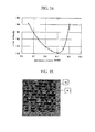
- FIG. 3 illustrates a recorded area 101 on a substrate of a commercially available DVD-R medium observed by an atomic force microscope (AFM), showing that the substrate 105 deforms toward the reflective layer 103 , which deformation leads to modulation
- AFM atomic force microscope
- JP-A Japanese Patent Application Laid-Open
- JP-A Japanese Patent Application Laid-Open
- No. 2001-181524 No. 2001-158865
- No. 2000-343824 No. 2000-343825
- No. 2000-335110 Examples of organic materials sensitive to blue-laser wavelengths can be found in Japanese Patent Application Laid-Open (JP-A) No. 2001-181524, No. 2001-158865, No. 2000-343824, No. 2000-343825, and No. 2000-335110.
- JP-A No. 11-221964, No. 11-334206, and No. 2000-43423 mention recording using an organic material in their examples but information is recorded at a wavelength of 488 nm. They only describe that satisfactory recording pits are formed and fail to teach the recording conditions and recording densities.
- JP-A No. 11-58955 mention recording using an organic material in the examples but information is recorded at a wavelength of 430 nm. It only describes that a satisfactory degree of modulation is obtained and fails to teach the recording conditions and recording densities.
- JP-A No. 2001-39034, No. 2000-149320, No. 2000-113504, No. 2000-108513, No. 2000-222772, No. 2000-218940, No. 2000-222771, No. 2000-158818, No. 2000-280621, and No. 2000-280620 mention recording using an organic material at a wavelength of 430 nm and a numerical aperture NA of 0.65. However, the information is recorded at a low recording density in terms of a minimum pit of 0.4 ⁇ m, equivalent to that in DVD media.
- JP-A No. 2001-146074 describes recording and/or reproducing at a wavelength of 405 to 408 nm but fails to teach a specific recording density.
- the recording herein is performed at a low density in which 14T-FEM signals are recorded.
- optical constants of the organic materials disclosed in the above publications at wavelengths around 405 nm are not equivalent to the required optical constant for recording layers of conventional write-once-read-many optical recording media.
- the publications fail to disclose examples in which information is recorded at a wavelength around 405 nm at a recording density higher than that in DVD media under specific conditions and fail to teach whether or not information can be recorded at a high density of 15 to 25 GB.
- most of the examples in the publications are performed using media of conventional configuration comprising a substrate, an organic material layer and a reflective layer, and colorants to be used therein must have optical properties and functions the same as conventional equivalents.
- Such conventional write-once-read-many optical recording media can use only organic materials having a high refractive index and a relatively low absorption coefficient of about 0.05 to about 0.10 for ensuring a satisfactorily high degree of modulation and reflectance.
- the organic materials have insufficient absorptivity to the recording light, the thickness of the resulting organic layer cannot be reduced so much, and a substrate having deep grooves must be used.
- a layer of an organic material is generally formed by spin coating, and such deep grooves are filled with the organic material to form a thick layer of the organic material.
- Such a substrate having deep grooves is difficult to prepare, and the resulting optical recording medium may have deteriorated quality.
- JP-A No. 07-304258 discloses a technique for recording information on a medium comprising a substrate, a layer containing a saturable absorption colorant and a reflective layer in this order based on the change of the extinction coefficient (the “absorption coefficient” as used in the present invention) of the saturable absorption colorant.
- JP-A No. 08-83439 discloses a technique for recording information on a medium comprising a substrate, a metal deposition layer, a light-absorptive layer and a protective sheet arranged in this order based on the discoloration or deformation of the metal deposition layer by action of heat generated from the light-absorptive layer.
- JP-A No. 08-138245 discloses a technique for recording information on a medium comprising a substrate, a dielectric layer, a recording layer containing a photoabsorption material, and a reflective layer arranged in this order by changing the thickness of the recording layer to thereby change the thickness of the grooves.
- JP-A No. 08-297838 discloses a technique for recording information on a medium comprising a substrate, a recording layer containing a photoabsorption material and a metal reflective layer arranged in this order by changing the thickness of the recording layer by a factor of 10 percent to 30 percent.
- JP-A No. 09-198714 discloses a technique for recording information on a medium comprising a substrate, a recording layer containing an organic colorant, a metal reflective layer and a protective layer arranged in this order by increasing the groove width of the substrate broader than an unrecorded area by a factor of 20 percent to 40 percent.
- JP-B Japanese Patent (JP-B) No. 2506374 discloses a technique for recording information on a medium comprising a substrate, an interlayer, and a metal thin film arranged in this order by deforming the metal thin layer to thereby form bubbles.
- JP-B No. 2591939 discloses a technique for recording information on a medium comprising a substrate, a light-absorptive layer, an auxiliary recording layer and an optical reflective layer by deforming the auxiliary recording layer to a concave shape and deforming the optical reflective layer to a concave shape along the deformation of the auxiliary recording layer.
- JP-B No. 2591940 discloses a technique for recording information on a medium comprising a substrate, a light-absorptive layer, a porous auxiliary recording layer and an optical reflective layer or comprising a substrate, a porous auxiliary recording layer, a light-absorptive layer and a reflective layer by deforming the auxiliary recording layer to a concave shape and deforming the reflective layer to a concave shape along the deformation of the auxiliary recording layer.
- JP-B No. 2591941 discloses a technique for recording information on a medium comprising a substrate, a porous light-absorptive layer, and a reflective layer arranged in this order by deforming the light-absorptive layer to a concave shape and deforming the reflective layer to a concave shape along the deformation of the auxiliary recording layer.
- JP-B No. 2982925 discloses a technique for recording information on a medium comprising a substrate, a recording layer containing an organic colorant and an auxiliary recording layer arranged in this order by allowing the auxiliary recording layer to mix with the organic colorant to thereby shift the absorption spectrum of the organic colorant to a shorter wavelength.
- JP-A No. 09-265660 discloses a technique for recording information on a medium comprising a substrate, a multi-function layer having functions as a reflective layer and a recording layer, and a protective layer arranged in this order by forming a bump between the substrate and the multi-function layer.
- the publication specifies metals such as nickel, chromium and titanium and alloys of these metals as the material for the multi-function layer.
- JP-A No. 10-134415 discloses a technique for recording information on a medium comprising a substrate, a metal thin layer, a deformable buffer layer, a reflective layer and a protective layer arranged in this order by deforming the substrate and the metal thin layer and reducing the thickness of the buffer layer in the deformed portion.
- the publication specifies metals such as nickel, chromium and titanium and alloys of these metals as the material for the metal thin layer and describes that a resin which is deformable and has an appropriate flowability is used in the buffer layer, which buffer layer may further comprise a colorant to accelerate the deformation.
- JP-A No. 11-306591 discloses a technique for recording information on a medium comprising a substrate, a metal thin layer, a buffer layer and a reflective layer arranged in this order by deforming the substrate and the metal thin layer and changing the thickness and optical constant of the buffer layer in the deformed portion.
- the publication describes that a metal such as nickel, chromium or titanium or an alloy thereof is preferably used in the metal thin layer and that the buffer layer comprises a mixture of a colorant and an organic polymer, which colorant has a large absorption band in the vicinity of the recording-reproducing wavelengths.
- JP-A No. 10-124926 discloses a technique for recording information on a medium comprising a substrate, a metal recording layer, a buffer layer and a reflective layer arranged in this order by deforming the substrate and the metal recording layer and changing the thickness and optical constant of the buffer layer in the deformed portion.
- the publication describes that a metal such as nickel, chromium or titanium or an alloy thereof is preferably used in the metal recording layer and that the buffer layer comprises a mixture of a colorant and a resin, which colorant has a great absorption band in the vicinity of the recording-reproducing wavelengths.
- TDK Corporation As a write-once-read-many optical recording medium according to “diffusion system”, for example, TDK Corporation has announced a medium having a configuration of a substrate, ZnS—SiO 2 , Si, Cu, ZnS—SiO 2 and Ag arranged in this order in CEATEC JAPAN 2003.
- the company has reported that the write-once-read-many optical recording medium has a degree of modulation of 65%, a jitter of 6% and a reflectance of 14%.
- An additional test made by the present inventors has revealed that when Si and Cu are arranged in adjacent layers, they gradually diffuse into another layer during storage and the recording medium shows deteriorated properties. This is a disadvantage of a medium in which components of two layers diffuse into and mix with each other.
- the medium requires two layers of a dielectric layer comprising ZnS—SiO 2 to yield a satisfactorily high degree of modulation and requires many processes and high cost.
- the ML (trademark; Multi Level) Technology has been proposed by Calimetrics, Inc. (CA) as a recording technique to increase conventional optical recording media.
- CA Calimetrics, Inc.
- the recording linear density is increased according to the ML Technology.
- each recording mark edge varies corresponding to a target data message in recording, and the length of the recording mark is determined in reproduction (slice system).
- the current slice system will be illustrated in short below.
- a recording mark row (c) is initially formed on an optical recording medium using a recording waveform (b) corresponding to a target recording data (a).
- Reproducing light is applied to the recording mark row (c) recorded on the optical recording medium to reproduce the information to thereby yield a reproducing signal waveform (d).
- the reproducing signal waveform (d) is a dull waveform different from the recording waveform (b), a rectangular pulse, and is thereby formatted using an equalizer to yield an equalized waveform (e). More specifically, high-frequency components of the reproducing signal are amplified.
- a binary data (f) is then outputted as one (1) when the point of intersection is detected within the window and as zero (0) when it is not detected.
- the binary data (f) obtained by the detection of point of intersection is converted according to a non-return-to-zero (NRZ) procedure to thereby yield a decoded data (g).
- a mark having a reflectance at multiple levels is recorded in a fixed-length area “cell”, and the information is indicated by the multi-level reflectance. More specifically, one bit is indicated by the presence or absence of a recording mark in the conventional CD or DVD optical recording media.
- recording marks are recorded at, for example, eight different levels of size and is read out as reflectance at eight different levels (FIG. 5 ).
- One recording mark indicates information corresponding to three bits, and the recording density can thereby be increased.
- bidirectional arrow 107 indicates the size of each cell.
- the beam spot diameter of laser light in reproduction is generally larger than the cell length, and one recording mark indicates information corresponding to three bits.
- the recording linear density can be increased to thereby increase the recording capacity without narrowing the track pitch.
- JP-A No. 2001-184647 discloses a concept of multi-level recording on an optical recording medium having a recording layer comprising an organic colorant and a concept of multi-level recording on the optical recording medium in a depth direction of the recording layer.
- this technique intends to provide a multi-level recordable write-once-read-many optical recording medium sensitive to red laser wavelengths, whose layer configuration and organic colorant used are the same as those of conventional CD or DVD write-once-read-many optical recording media.
- Aforementioned JP-A No. 2002-25114 discloses a multi-level recordable optical recording medium including a substrate and a recording layer of an organic colorant, which substrate has a specific glass transition point, reflectance and thermal conductivity.
- Aforementioned JP-A No. 2002-83445 discloses a multi-level recordable optical recording medium including a recording layer comprising an organic colorant, which organic colorant has specific thermal decomposition properties.
- Aforementioned JP-A No. 2002-334438 and No. 2002-352428 each disclose a multi-level recordable optical recording medium having a recording layer comprising phthalocyanine or cyanine colorant, in which the relationships among the wavelength, numeral aperture NA and groove width are specified.
- Aforementioned JP-A No. 2002-352429 discloses a multi-level recordable optical recording medium having a recording layer comprising an organic colorant, in which the relationship between the thickness of the recording layer on a groove and the groove depth is specified.
- Aforementioned JP-A No. 2002-367182 discloses a multi-level recordable optical recording medium having a recording layer comprising an organic colorant, in which the reflectance in an unrecorded area is specified within a range of 40% to 80%.
- the cell length in the multi-level recording must be reduced to the same level as the minimum mark length in the conventional binary recording. Namely, the minimum mark in the multi-level recording is much shorter (smaller) than the minimum mark in the binary recording.
- the aforementioned conventional technologies employ conventional recording materials and layer configurations in multi-level recording, although some of conditions such as the thickness of the recording layer and the material of the reflective layer are slightly modified. They cannot form shorter recording marks than conventional equivalents and cannot record and reproduce recording marks much smaller than conventional equivalents with a higher reliability. In short, they only achieve the reproduction of a somewhat smaller recording mark with good reliability by action of the recording and reproducing techniques, and simply apply the recording and reproducing techniques to write-once-read-many optical recording media.
- the conventional techniques form recording marks typically by means of deformation (FIG. 3 ).
- the deformation presents no problem when the pitch between recording marks is sufficiently long, i.e., the recording linear density is low, or when the length of a cell in which a multi-level record is formed is not longer than the beam diameter of the reproducing light.
- the deformations interfere with each other and the interference becomes nonlinear when the recording linear density is high or when the length of a cell in which a multi-level record is formed is longer than the beam diameter of the reproducing light.
- FIGS. 6A , 6 B and 6 C are a plan view, a sectional view, and a sectional view as a sum, respectively of three recording marks which are formed in successive three cells mainly by means of deformation without interference.
- FIGS. 7O , 7 A, 7 B, 7 C, 7 D and 7 E schematically illustrate a reproducing signal which varies depending on the difference of interference among the deformations in three cells.
- three recording marks are formed in successive three cells mainly by means of deformation and the total length of the three recorded cells is smaller than the diameter 109 of reproducing beam. If the interference in deformation is linear, the resulting deformation is as shown in FIG. 7 B. However, if the interference in deformation is not linear, the resulting deformation is modified as shown in FIG. 7C or FIG. 7 D.
- the interfered deformation has a length smaller than the diameter 109 of reproducing beam, and the difference in the deformation is therefore not detected. Accordingly, a reproducing signal as shown in FIG. 7E can be substantially obtained even when the deformation varies as shown in FIGS. 7B , 7 C and 7 D.
- Exact data can therefore be decoded by detecting the reflection levels at sampling times T 1 , T 2 and T 3 shown in FIG. 7 E.
- FIGS. 8O , 8 A, 8 B, 8 C, 8 D, 8 E, 8 F and 8 G schematically illustrate the relationship between the interference in deformation and the reproducing signal when successive seven recording marks mainly based on deformation are formed in successive seven cells and the total length of the cells is larger than the diameter 109 of reproducing beam.
- the interference in deformation in this case becomes more nonlinear than the case shown in FIGS. 7B , 7 C and 7 D, and the interfered deformation is as shown in FIGS. 8B , 8 C and 8 D when simply illustrated.
- the interfered deformations each have a length larger than the diameter 109 of reproducing beam, and the difference among the deformations can be clearly detected.
- reproducing signals shown in FIGS. 8E , 8 F and 8 G are obtained from the deformations in FIGS. 8B , 8 C and 8 D, respectively.
- the reproducing signal has a dull waveform.
- the reproducing signal waveform (d) is not a rectangular waveform as in the recording waveform (b).
- the high frequency components of the reproducing signal are amplified using an equalizer and the reproducing signal is converted to have an equalized waveform.
- the reproducing signal has a dull waveform with an increasing density, a larger quantity of high frequency components must be amplified.
- signal degrading components are also amplified by the equalizer, thus inviting significantly decreased signal-to-noise ratio (SNR) of the reproducing signal.
- PRML is a reproducing signal processing system to prevent SNR of the reproducing signal from decreasing even in high density recording.
- the PRML system will be briefly illustrated below.
- FIG. 9 illustrates a recording data (a) as target information, a recording waveform (b), a recording mark row (c), a reproducing signal waveform (d) and equalized waveforms (e), (f) and (g).
- the equalized waveforms (e), (f) and (g) are obtained as a result of equalization of the reproducing waveform (d) by an equalizer depending on PR(1,1) characteristic, PR(1,2,1) characteristic and PR(1,2,2,1) characteristic, respectively.
- the PR(1,1) characteristic is a characteristic in which an impulse response appears at the rate of 1:1 at two successive identification points.
- the PR(1,2,1) characteristic is a characteristic in which an impulse response appears at the rate of 1:2:1 at three successive identification points.
- the PR(1,2,2,1) characteristic is a characteristic in which an impulse response appears at the rate of 1:2:2:1 at four successive identification points.
- the equalized waveforms (e), (f) and (g) in FIG. 9 show that an equalized waveform becomes duller with an increasing complexity of the PR characteristic.
- an increase in the signal degrading component in the equalizer can be suppressed by equalizing the reproduced waveform into a waveform of a PR characteristic which is closer to the characteristic of the reproduced waveform.
- a Viterbi decoder which is a representative one of maximum likelihood decoders is generally used as a most-likelihood decoder in decoding of the equalized waveform signals. For example, if the reproduced waveform is equalized into a waveform of the PR(1,2,1) characteristic by the equalizer, the Viterbi decoder selects a series having the smallest error with respect to the sample series of the equalized waveform from all of the reproduced waveform series which satisfy the PR(1,2,1) characteristic and estimates and outputs recording data (binary data, decoded data) used as a source for generating the selected reproduced waveform series.
- the PRML system realizes high-density recording even using a conventional optical system.
- the PRML system cannot record and reproduce information with high reliability when the interference among recording marks (intersymbol interference) becomes large and becomes nonlinear, namely, when a predictable interference among recording marks occurs.
- the PRML system can be applied onto to such a case in which a predictable interference among recording marks occurs. If an interference among recording marks different from the predicted one occurs, the advantages of the PRML system are not obtained.
- the deformation of recording marks must be prevented to suppress the interference among recording marks at a predictable level.
- write-once-read-many optical recording media on which information can be recorded by multi-level recording at a wavelength of blue-laser wavelengths or shorter, recording marks with higher quality than those obtained by the conventional binary recording technique can be formed.
- Information can be recorded on the resulting write-once-read-many optical recording media by the conventional binary recording technique at a wavelength of blue-laser wavelengths or shorter and also by multi-level recording at a higher density by the application of the PRML system.
- Requirements to achieve write-once-read-many optical recording media sensitive to blue-laser wavelengths or shorter wavelengths can be considered as requirements to provide write-once-read-many optical recording media that allow multi-level recording at a wavelength of blue-laser wavelengths or shorter.
- the requirements to write-once-read-many optical recording media that allow multi-level recording at a wavelength of blue-laser wavelengths or shorter are the following requirements (1), (2) and (3):
- the minimum mark has a sufficient size with respect to the diameter of reproducing beam (approximately half the diameter of reproducing beam), the amplitude derived from the minimum mark is sufficiently large, and the deformation in the minimum mark is large.
- the minimum mark has an insufficient size with respect to the diameter of reproducing beam, and the amplitude derived from the minimum mark in multi-level recording is approximately one-half to one-tenths or less the amplitude derived from the minimum mark in binary recording, and the deformation in the minimum mark is very small.
- Conventional CD or DVD write-once-read-many optical recording media have a layer of an organic colorant having optical absorptivity arranged directly adjacent to a substrate.
- the substrate deforms to a large extent.
- the degree of modulation is primarily affected by the deformation of substrate and is secondarily affected by the decomposition of the organic colorant.
- a deformation of the substrate within an elastic deformation region may be relieved, for example, by extraneous heat.
- a deformation of the substrate exceeding the elastic deformation region is limited, but its shape may significantly vary with the heat applied upon the formation of an adjacent recording mark or with the deformation of the adjacent recording mark.
- FIGS. 10 and 11 illustrate these phenomena.
- FIG. 10 shows recording marks in a write-once-read-many optical recording medium having a conventional structure of a substrate, a colorant layer, an Ag reflective layer and a protective layer arranged in this order.
- FIG. 10 illustrates a waveform A of a reproducing signal; an atomic force micrographic (AFM) image B of the surface of the substrate after removing the protective layer, Ag reflective layer and colorant layer; and a deformation C of the cross section of the substrate as determined based on the AFM image B.
- FIG. 10 shows that the recorded area is much largely deformed with a concave shape at a center part of the recording mark.
- the interference in deformation is nonlinear, as illustrated in FIGS. 7C , 7 D, 8 C and 8 D.
- FIG. 11 illustrates recording marks obtained by recording the information as in FIG. 10 on the conventional write-once-read-many optical recording medium and applying a weak direct-current light of about one-fifths of the recording power to the medium.
- FIG. 11 illustrates a waveform A of a reproducing signal; an atomic force micrographic (AFM) image B of the surface of the substrate after removing the protective layer, Ag reflective layer and colorant layer; and a deformation C of the cross section of the substrate as determined based on the AFM image B.
- FIG. 11 shows that the deformation of substrate changes and thus the waveform of the reproducing signal changes upon irradiation of the weak direct-current light. This is probably because the application of the weak direct-current light relieves the strain in the deformed portion of the substrate.
- the conventional write-once-read-many optical recording media each having a recording layer comprising an organic material have the following disadvantages (i), (ii), (iii) and (iv):
- an object of the present invention is to solve these problems and to provide a write-once-read-many optical recording medium that can yield a high degree of modulation by recording marks with small deformation and to provide a process for recording and/or reproducing information for the medium.
- the present invention provides a write-once-read-many optical recording medium containing a first inorganic thin film; and at least one of a second inorganic thin film and an organic thin film, wherein the first inorganic thin film comprises at least “R” and “O,” wherein “R” represents at least one selected from the group consisting of Y, Bi, In, Mo, V and lanthanum series elements; and “O” represents oxygen atom, and the second inorganic thin film and the organic thin film are capable of suppressing at least one of deformation and breakage of the first inorganic thin film and receiving the change of state of the first inorganic thin film.
- Information can be easily recorded on the write-once-read-many optical recording medium of the present invention at high density by binary recording or multi-level recording even at blue-laser wavelengths of 500 nm or less, typically at wavelengths around 405 nm.
- the write-once-read-many optical recording medium may contain at least the first inorganic thin film and the organic thin film in a first aspect, may contain at least the first inorganic thin film and the second inorganic thin film in a second aspect and may contain at least the first inorganic thin film, the second inorganic thin film and the organic thin film in a third aspect.
- the present invention further provides a process for recording and/or reproducing information on the write-once-read-many optical recording medium, the process including forming a recorded area by the photoabsorption function of at least one of the first inorganic thin film and the organic thin film at wavelengths at which recording and reproduction is performed.
- the process of the present invention can easily record and reproduce information on the write-once-read-many optical recording medium at a high density by binary recording or multi-level recording even at blue-laser wavelengths of 500 nm or less, typically at wavelengths around 405 nm.
- FIG. 1 is a diagram showing the relationship between the recording-reproducing wavelengths and the major absorption band of an organic material in a recording layer of a conventional write-once-read-many optical recording medium.
- FIG. 2 is a diagram showing a large dependency on wavelength of the optical constant of the conventional write-once-read-many optical recording medium.
- FIG. 3 is an atomic force micrograph of the deformation of the substrate of the conventional write-once-read-many optical recording medium.
- FIG. 4 is an illustration of data decoding according to a conventional level slice system and shows a recording data (a) as a target information, a recording waveform (b) corresponding to the recording data (a), a recording mark row (c) formed in an optical recording medium, a reproducing signal waveform (d) of the recording mark row (c), an equalized waveform (e) as a result of equalization of the reproducing signal waveform (d) by an equalizer, a binary data (f) obtained by detecting the point of intersection of the equalized waveform (e) and the threshold, and a decoded data (g) obtained by subjecting the binary data (f) to NRZ conversion.
- FIG. 5 is a schematic diagram of recording marks in multi-level recording.
- FIGS. 6A , 6 B and 6 C are a plan view, a sectional view of deformation without interference, and a sectional view of added deformation, respectively, of three recording marks formed in three successive cells mainly based on deformation and show linear interference in deformation.
- FIGS. 7O , 7 A, 7 B, 7 C, 7 D and 7 E are diagrams showing different reproducing signals due to different interference in deformation of three recording marks formed in three successive cells mainly based on deformation when the total length of the recorded cells is smaller than the diameter of reproducing beam, in which FIG. 7O illustrates the diameter of reproducing beam, FIG. 7A is a plan view of the recording marks, FIG. 7B illustrates an added deformation, FIGS. 7C and 7D illustrate a nonlinearly interfered deformation, respectively, and FIG. 7E illustrates a reproducing signal obtained in the cases of FIGS. 7B , 7 C and 7 D.
- FIGS. 8O , 8 A, 8 B, 8 C, 8 D, 8 E, 8 F and 8 G are diagrams showing different reproducing signals due to different interference in deformation of seven recording marks formed mainly based on deformation in seven successive cells when the total length of the recorded cells is larger than the diameter of reproducing beam, in which FIG. 8O illustrates the diameter of reproducing beam, FIG. 8A is a plan view of the recording marks, FIG. 8B illustrates an added deformation, FIGS. 8C and 8D illustrate a nonlinearly interfered deformation, respectively, and FIGS. 8E , 8 F and 8 G illustrate a reproducing signal obtained in the cases of FIGS. 8B , 8 C and 8 D, respectively.
- FIG. 9 is a diagram showing data decoding according to the PRML system and shows a recording data (a) as a target information, a recording waveform (b) corresponding to the recording data (a), a recording mark row (c) formed in an optical recording medium, a reproducing signal waveform (d) of the recording mark row (c), an equalized waveform (e) as a result of equalization of the reproducing signal waveform (d) based on the PR(1,1) characteristic by an equalizer, an equalized waveform (f) as a result of equalization of the reproducing signal waveform (d) based on the PR(1,2,1) characteristic by the equalizer, and an equalized waveform (g) as a result of equalization of the reproducing signal waveform (d) based on the PR(1,2,2,1) characteristic by the equalizer.
- FIG. 10 is a diagram showing the relationship between the deformation of a substrate and the reproducing signal of a conventional write-once-read-many optical recording medium.
- FIG. 11 is a diagram showing the relationship between the deformation of a substrate and the reproducing signal of a conventional write-once-read-many optical recording medium when a weak DC light is applied to the medium after recording.
- FIG. 12 is a diagram showing the relationship between the major absorption band and the recording-reproducing wavelengths of a write-once-read-many optical recording medium of the present invention.
- FIG. 13 is a diagram illustrating the “major absorption band” as used in the present invention.
- FIG. 14 is a diagram showing binary recording on a write-once-read-many optical recording medium according to Example 1-1.
- FIG. 15 is an AFM image of deformation of the substrate of a write-once-read-many optical recording medium according to Comparative Example 1-1.
- FIG. 16 is a diagram showing eight-level recording on a write-once-read-many optical recording medium according to Example 1-8.
- FIG. 17 is a diagram showing eight-level recording on a write-once-read-many optical recording medium according to Comparative Example 1-2.
- FIGS. 18A and 18B are an AFM image and a cross sectional view along the lines L—L of FIG. 18A , respectively, of deformed substrate of a write-once-read-many optical recording medium according to Comparative Example 1-2.
- FIG. 19 is a diagram showing the relationship between the deformation height on the surface of substrate and the amount of drops of a write-once-read-many optical recording medium according to Comparative Example 1-2.
- FIG. 20 is a diagram showing eight-level recording on a write-once-read-many optical recording medium according to Example 1-9.
- FIG. 21 is a diagram of scanning electron microscopic observation of the BiFeO surface of the write-once-read-many optical recording medium according to Example 1-9.
- FIG. 22 is a diagram showing absorption factors Q of write-once-read-many optical recording media according to Example 1-1 and Comparative Example 1-1 and of a commercially available CD-R medium.
- FIG. 23 is a transmission electron micrograph of a recorded area of a write-once-read-many optical recording medium according to Example 1-1 as a specimen cut by focused ion beam (FIB).
- FIB focused ion beam
- FIG. 24 is a diagram showing binary recording on a write-once-read-many optical recording medium according to Example 2-1-2.
- FIG. 25 is a diagram showing binary recording on a write-once-read-many optical recording medium according to Example 2-1-1.
- FIG. 26 shows jitters of write-once-read-many optical recording media according to Example 2-1-1 and Example 2-1-2, respectively.
- FIG. 27 is a diagram of reproducing signal levels in the space and recording marks of the write-once-read-many optical recording media according to Example 2-1-1 and Example 2-1-2, respectively.
- FIG. 28 is an AFM image of a deformed substrate of a write-once-read-many optical recording medium according to Comparative Example 2-1.
- FIG. 29 is a diagram showing the relationship between the recording power and the jitter ( ⁇ /Tw) of a write-once-read-many optical recording medium according to Example 2-20 in one track recording at a varying minimum mark length (2T).
- FIG. 30 is a diagram showing the relationship between the recording power and the jitter ( ⁇ /Tw) of the write-once-read-many optical recording medium according to Example 2-20 in continuous recording at a varying minimum mark length (2T).
- FIG. 31 is a diagram showing the suitability for high-density recording of write-once-read-many optical recording media according to Example 2-1-1 and Comparative Example 2-1.
- FIG. 32 is a diagram showing the suitability for high-density recording of write-once-read-many optical recording media according to Example 2-11 and Comparative Example 2-1.
- FIG. 37 is a diagram showing eight-level recording on a write-once-read-many optical recording medium according to Example 2-1-1.
- FIG. 38 is a diagram showing eight-level recording on a write-once-read-many optical recording medium according to Comparative Example 2-3.
- FIGS. 39A and 39B are an AFM image of the surface and a cross sectional view taken along the lines L—L of FIG. 39A , respectively, of a substrate of a write-once-read-many optical recording medium according to Comparative Example 2-3.
- FIG. 40 is a diagram showing the relationship between a deformation height and the drops in degree of modulation of a write-once-read-many optical recording medium according to Comparative Example 2-3.
- FIG. 41 is a diagram showing eight-level recording on a write-once-read-many optical recording medium according to Example 2-30.
- FIG. 42 is a scanning electron micrograph of deformation of a BiFeO surface of the write-once-read-many optical recording medium according to Example 2-30.
- FIG. 43 is a scanning electron micrograph of deformation of a BiFeO surface of the write-once-read-many optical recording medium according to Example 2-31.
- FIG. 44 is a diagram showing a reproducing signal obtained from a write-once-read-many optical recording medium according to Example 2-31.
- FIG. 45 is a scanning electron micrograph of deformation of a BiFeO surface of the write-once-read-many optical recording medium according to Comparative Example 2-4 at a cell length of 0.32 ⁇ m.
- FIG. 46 is a diagram showing a reproducing signal obtained from a write-once-read-many optical recording medium according to Comparative Example 2-4 at a cell length of 0.32 ⁇ m.
- FIG. 47 is a scanning electron micrograph of deformation of a BiFeO surface of the write-once-read-many optical recording medium according to Comparative Example 2-4 at a cell length of 0.24 ⁇ m.
- FIG. 48 is a diagram showing a reproducing signal obtained from a write-once-read-many optical recording medium according to Comparative Example 2-4 at a cell length of 0.24 ⁇ m.
- FIG. 49 is a scanning electron micrograph of deformation of a BiO surface of a write-once-read-many optical recording medium according to Example 2-32.
- FIG. 50 is a diagram showing a reproducing signal obtained from a write-once-read-many optical recording medium according to Example 2-32.
- FIG. 51 is a diagram showing absorption factors Q of write-once-read-many optical recording media according to Example 2-1-1 and Comparative Example 2-1 and of a commercially available CD-R medium.
- FIG. 52 is a diagram showing absorption factors Q of write-once-read-many optical recording media according to Example 2-23 and Comparative Example 2-1 and of a commercially available CD-R medium.
- FIG. 53 is a transmission electron micrograph of a recorded area of a write-once-read-many optical recording medium according to Example 2-1-1 as a specimen cut in a radius direction by focused ion beam (FIB).
- FIB focused ion beam
- FIG. 54 is a transmission electron micrograph of a recorded area of a write-once-read-many optical recording medium according to Example 2-1-2 as a specimen cut in a radius direction by focused ion beam (FIB).
- FIB focused ion beam
- FIG. 55 is a transmission electron micrograph of a recorded area of a write-once-read-many optical recording medium according to Example 2-31 as a specimen cut in a guide groove direction by focused ion beam (FIB).
- FIB focused ion beam
- FIG. 56 is a transmission electron micrograph of an unrecorded area of a write-once-read-many optical recording medium according to Example 2-42 as a specimen cut in a radius direction by focused ion beam (FIB).
- FIB focused ion beam
- FIG. 57 is a transmission electron micrograph of a recorded area of a write-once-read-many optical recording medium according to Example 2-42 as a specimen cut in a radius direction by focused ion beam (FIB).
- FIB focused ion beam
- FIG. 58 is a diagram showing the relationship between x/(x+y) and the jitter ( ⁇ /Tw) in conventional binary recording on a write-once-read-many optical recording medium according to Example 2-14.
- FIG. 59 is a diagram showing the relationships among x/(x+y), the degree of modulation and the reflectance in conventional binary recording on a write-once-read-many optical recording medium according to Example 2-14.
- FIG. 60 is a diagram showing the relationship between the recording power and the jitter in conventional binary recording on a write-once-read-many optical recording medium according to Example 2-19.
- FIG. 61 is a diagram showing the relationship between the recording power and the jitter in conventional binary recording on a write-once-read-many optical recording medium according to Example 2-28.
- FIG. 62 is a diagram showing an eye pattern (eye diagram) in conventional binary recording on a write-once-read-many optical recording medium according to Example 2-28.
- FIG. 63 is a diagram showing the sigma to dynamic range (SDR) at different cell lengths in multi-level recording on a write-once-read-many optical recording medium according to Example 2-33.
- the write-once-read-many optical recording media according to the present invention each comprise a first inorganic thin film, and at least one of a second inorganic thin film and an organic thin film and may further comprise a reflective layer, a cover layer and other layers according to necessity.
- the write-once-read-many optical recording medium comprises at least the first inorganic thin film such as an RO film, wherein “R” is an element as mentioned below and “O” is oxygen atom, and the organic thin film and may further comprise a reflective layer, a cover layer and other layers according to necessity.
- the write-once-read-many optical recording medium comprises at least the first inorganic thin film and the second inorganic thin film and may further comprise a reflective layer, a cover layer and other layers according to necessity.
- the write-once-read-many optical recording medium comprises at least the first inorganic thin film, the second inorganic thin film and the organic thin film and may further comprise a reflective layer, a cover layer and other layers according to necessity.
- a write-once-read-many optical recording medium comprising, for example, a substrate, the first inorganic thin film such as an RO film, the organic thin film and the reflective layer arranged in this order
- the thickness of the first inorganic thin film and the organic thin film must be optimized. If not, the first inorganic thin film largely deforms and may break in some cases.
- a write-once-read-many optical recording medium having the above configuration can yield satisfactory recording-reproducing properties in the vicinity of the optimum recording power, but its first inorganic thin film largely deforms, may break in some cases and the medium shows decreased margins of the jitter and error rate at a recording power higher than the optimum recording power. More specifically, the medium shows a rapidly and discontinuously increasing degree of modulation with an increasing recording power.
- the deformation increasingly affects the properties of the medium not only with an increasing recording power but also with an increasing recording mark length. Therefore, the asymmetry may be deteriorated to a negative region under such recording conditions as to yield the optimum jitter and error rate.
- recording on the first inorganic thin film in the medium having this configuration is performed mainly by a recording mechanism accompanied with a relatively large change such as deformation and fusing.
- this configuration may often invite a relatively large change such as deformation and fusing of the first inorganic thin film in recording.
- the substrate is arranged in direct contact with the first inorganic thin film, and a large quantity of heat propagates into the substrate. Thus, the substrate expands and deforms to thereby further deform the first inorganic thin film, which may invite breakage of the first inorganic thin film.
- the medium of the present invention may preferably further comprise the second inorganic thin film in addition to the first inorganic thin film.
- the second inorganic thin film works to suppress at least one of the deformation and breakage of the first inorganic thin film and to receive the change of state of the first inorganic thin film, such as fusing, change in composition, diffusion, change in crystalline state, oxidation and/or reduction.
- the second inorganic thin film may preferably be arranged adjacent to the first inorganic thin film to effectively exhibit the aforementioned functions. However, it can also exhibit its functions even when another layer is interposed between the first inorganic thin film and the second inorganic thin film.
- the second inorganic thin film herein works to suppress at least one of the deformation and breakage of the first inorganic thin film and to receive the change of state of the first inorganic thin film, such as fusing, change in composition, diffusion, change in crystalline state, oxidation and/or reduction.
- the absorption coefficient at the recording-reproducing wavelengths is reduced by at least one of decomposition and degradation of the organic material, and the resulting large change in refractive index is used to modulate the amplitude.
- An organic material layer used herein works as a heat generation layer due to its optical absorptivity and as a recording layer based on change in refractive index (a real part of complex refractive index) caused by the decomposition and/or degradation.
- a function as a main heat generation layer is separated from such a conventional organic thin film, the first inorganic thin film having photoabsorptivity is formed in addition to the organic thin film, and the second inorganic thin film is further formed.
- recording marks are formed based on at least one of the following mechanisms (1) to (11):
- Preferred recording mechanisms to form recording marks are those relating to the change of state of at least one of the first inorganic thin film and the second inorganic thin film, i.e., the recording mechanisms (1) to (8), of which recording mechanisms (2) to (8) are more preferred.
- the “change of state” such as change in composition, fusing, change in crystalline state, oxidation and/or reduction, diffusion of constitutional elements into an adjacent layer can be utilized.
- the first inorganic thin film can have a significantly varied complex refractive index and can have an unclear interface with the adjacent layer to thereby reduce the influence of multiple reflection. Accordingly, a high degree of modulation can be yielded even with a small deformation.
- information can be recorded not mainly based on deformation but mainly based on any of the above recording mechanisms.
- the first inorganic thin film performs a major photoabsorption function.
- the first inorganic thin film exhibits normal dispersion, does not have a large absorption band within a range of certain wavelengths and its complex refractive index less depends on wavelength, in contrast to organic materials. Accordingly, the use of the first inorganic thin film can suppress large variation of recording properties such as recording sensitivity, degree of modulation, jitter and error rate and of reflectance even with varying recording-reproducing wavelengths derived from the individual difference of laser or varying environmental temperature.
- the organic thin film performs both functions as a recording layer and a light-absorptive layer.
- the constitutional organic material must thereby have a high refractive index n and a relatively low absorption coefficient k at the recording-reproducing wavelengths.
- the organic thin film must have a relatively large thickness to reach a temperature at which the organic material decomposes.
- the substrate In a phase-change optical recording medium, the substrate must have very deep grooves.
- the organic thin film can have a smaller thickness than conventional equivalents.
- the organic thin film having such a smaller thickness realizes the use of a substrate having shallow grooves and thus having satisfactory transfer ability (moldability).
- This type of substrate can be more easily prepared at lower cost than conventional equivalents.
- the resulting optical recording media have significantly improved signal quality.
- Reproduction according to any of the aforementioned recording mechanisms is impervious to the shape of grooves in the substrate and has a large allowance (margin) with respect to variation of the shape of substrate.
- This type of substrate can be more easily prepared at lower cost than conventional equivalents.
- the organic thin film having such a smaller thickness realizes broader recording power margins.
- the first inorganic thin film performs a photoabsorption function as well as a recording function.
- the photoabsorption function of the first inorganic thin film causes any of the following changes of state of the first inorganic thin film itself:
- the first inorganic thin film preferably comprises an element capable of absorbing light at a recording-reproducing wavelength of 500 nm or less as element R and/or M.
- the first inorganic thin film preferably comprises, as Element R, an element having a relatively low melting point as an elementary substance or as an oxide.
- Element R of the first inorganic thin film should be at least one selected from Y, Bi, In, Mo, V and lanthanum series elements.
- bismuth oxide BiO wherein “R” is Bi
- a mixture of bismuth and bismuth oxide are preferred for multi-level recording.
- the first inorganic thin film preferably further comprises at least one element M selected from Al, Cr, Mn, Sc, In, Ru, Rh, Co, Fe, Cu, Ni, Zn, Li, Si, Ge, Zr, Ti, Hf, Sn, Pb, Mo, V and Nb.
- the presence of an oxide can increase the hardness of the first inorganic thin film to thereby suppress the deformation of the first inorganic thin film itself and/or of an adjacent layer such as the substrate.
- a satisfactory inorganic thin film can be prepared by a vapor phase epitaxy such as sputtering.
- the ratio of “x” to the total of “x” and “y” [x/(x+y)] is preferably 0.3 or more.
- Element R is preferably Bi for further better recording-reproducing properties.
- the first inorganic thin film is preferably represented by Bi a (4B) b O d or Bi a (4B) b X c O d , wherein “4B” is at least one of Group 4B elements of the Periodic Table of Elements for better recording-reproducing properties and for better storage stability. Examples of Group 4B elements are C, Si, Ge, Sn and Pb, of which Si and Ge are typically preferred. “X” is at least one element selected from Al, Cr, Mn, In, Co, Fe, Cu, Ni, Zn, Ti and Sn.
- the element “X” works to cause a larger change in complex refractive index or in composition, to cause fusing or to yield a further diffusion of constitutional elements into an adjacent layer.
- the first inorganic thin film may comprise the oxide RO alone but may further comprise Element R in another form than an oxide (this form of element other than an oxide is hereinafter referred to as “elementary”), in addition to RO (oxide of Element R) (hereinafter referred to as “R+RO”).
- the first inorganic thin film further comprises Element M in addition to R and O
- these elements may be contained as at least one of (1) a ternary compound of R—M—O, (2) a mixture of the elementary R and an oxide of Element M (R+MO), (3) a mixture comprising an oxide of Element R and an oxide of Element M (RO+MO), (4) a mixture of Element R, an oxide of Element R, and an oxide of Element M (R+RO+MO), and a combination of configurations (1) to (4).
- the “first inorganic thin film” for use in the present invention may comprise any of compounds, elements, and mixtures as mentioned above.
- oxidation of Element R not in the state of oxide upon recording can significantly change the complex refractive index of the first inorganic thin film.
- information can be recorded not based on deformation and can be recorded with less intersymbol interference.
- first inorganic thin film contains a large amount of Element R and/or Element M not in the state of oxide, the medium may have decreased storage stability.
- the content of elementary R and/or elementary M is preferably lower than the content of the oxide of Element R and/or the oxide of Element M.
- the ratio of the former to the latter is preferably set according to the balance of properties such as recording sensitivity, jitter and storage stability.
- Element R and/or an oxide thereof performs a major photoabsorption function and a recording function, and above specified elements as Element R can exhibit specific advantages.
- the ratio [x/(x+y)] is preferably 0.3 or more for better recording-reproducing properties.
- a first inorganic thin film having a ratio [x/(x+y)] less than 0.3 can be used for fine control of recording-reproducing properties and storage stability.
- the ratio [x/(x+y)] is not limited to the range of 0.3 or more in the present invention.
- the first inorganic thin film preferably has a thickness of 20 to 500 angstroms (2-50 nm).
- the second inorganic thin film functions to suppress the deformation and/or breakage of the first inorganic thin film and to receive change of state of the first inorganic thin film, such as fusing, change in composition, diffusion, change in crystalline state, oxidation and/or reduction.
- the first inorganic thin film is capable of absorbing light in a relatively large quantity at the recording-reproducing wavelengths and generally has a relatively small thickness for better reflectance, although the thickness of the first inorganic thin film may be set according to its absorption coefficient.
- a first inorganic thin film having a small thickness arranged directly in contact with the substrate may largely deform or break due to expansion of the substrate, even though the film has a high hardness.
- the second inorganic thin film is used to suppress the deformation and/or breakage of the first inorganic thin film in the present invention.
- the second inorganic thin film may be arranged between the substrate and the first inorganic thin film to effectively suppress the deformation and/or breakage of the first inorganic thin film.
- the advantages of the second inorganic thin film can also be obtained even if the medium comprises the substrate, the first inorganic thin film and the second inorganic thin film arranged in this order. This is probably because the first inorganic thin film has a relatively small thickness, and the second inorganic thin film can easily exhibit its advantages through such a thin first inorganic thin film.
- the second inorganic thin film performs a recording function in addition to the function of suppressing the deformation and/or breakage of the first inorganic thin film.
- information is recorded on the write-once-read-many optical recording media of the present invention, for example, by:
- the second inorganic thin film When the second inorganic thin film is arranged adjacent to the first inorganic thin film, it functions to receive the change of state of the first inorganic thin film and to have an unclear interface with the first inorganic thin film.
- Such an “unclear interface” means that the interface between the two thin films becomes a different state from that before recording.
- the unclear interface means that the complex refractive index becomes gradient in the vicinity of the interface between the first inorganic thin film and the second inorganic thin film typically by mixing or diffusion of components of the first inorganic thin film and the second inorganic thin film at the interface.
- the complex refractive index varies discontinuously at the interface in an unrecorded area but varies gradually in the vicinity of the interface in a recorded area.
- the second inorganic thin film can receive the change of state of the first inorganic thin film such as fusing, change in composition, diffusion, change in crystalline state, oxidation and/or reduction and make the interface between the first inorganic thin film and the second inorganic thin film unclear.
- the influence of, for example, multiple reflection can be suppressed to thereby yield a high degree of modulation.
- the second inorganic thin film has another essential function to control its thermal conductivity. Thus, fine recording marks with less variation can be efficiently formed.
- the second inorganic thin film further functions to control the reflectance, tracking signals and recording sensitivity by appropriately selecting the material and thickness thereof.
- Materials that do not undergo decomposition, sublimation or formation of cavities due to heat generated from the first inorganic thin film are preferably used in the second inorganic thin film.
- examples of such materials are Al 2 O 3 , MgO, BeO, ZrO 2 , UO 2 , ThO 2 and other simple oxides; SiO 2 , 2MgO—SiO 2 , MgO—SiO 2 , CaO—SiO 3 , ZrO 2 —SiO 2 , 3Al 2 O 3 —2SiO 2 , 2MgO-2Al 2 O 3 —5SiO 2 , Li 2 O—Al 2 O 3 —4SiO 2 and other silicate-containing oxides; Al 2 TiO 5 , MgAl 2 O 4 , Ca 10 (PO 4 ) 6 (OH) 2 , BaTiO 3 , LiNbO 3 , PZT [Pb(Zr,Ti)O 3 ], PLZT [(
- the second inorganic thin film preferably mainly comprises SiO 2 , ZnS or ZnS—SiO 2 for better optical transparency to the recording-reproducing light or for better productivity. It may also preferably mainly comprise ZrO 2 for sufficient thermal insulation. It may also preferably comprise an oxide selected from ZnS, ZrO 2 , Y 2 O 3 and SiO 2 or an oxide comprising ZrO 2 , TiO 2 , SiO 2 and “X,” wherein “X” is at least one selected from Y 2 O 3 , CeO, Al 2 O 3 , MgO, CaO, NbO and oxide of rare earth metals.
- the thermal conductivity and hardness of the second inorganic thin film play an important role to effectively receive the change of state of the first inorganic thin film, such as fusing, change in composition, diffusion, change in crystalline state, oxidation and/or reduction.
- the second inorganic thin film preferably mainly comprises ZnS. If it comprises ZnS—SiO 2 , the ratio of ZnS is preferably increased.
- the medium may further comprise a sulfuration-resistant layer for preventing sulfuration of Ag.
- the second inorganic thin film is preferably transparent to light at the recording-reproducing wavelengths for higher reflectance. However, it can have some function for absorbing light at the recording-reproducing wavelength for controlling recording sensitivity.
- the second inorganic thin film preferably has a thickness of 20 to 2000 angstroms (2-200 nm) and generally preferably has a thickness larger than that of the first inorganic thin film.
- Functions of the organic thin film are roughly classified as (a) a heat insulating function typically in a configuration in which the organic thin film is sandwiched between the reflective layer and the first inorganic thin film; (b) a function of yielding a high degree of modulation; (c) a function of compensating the reproducing signal waveform; (d) a function of controlling, for example, the reflectance and tracking signals; and (e) a function of controlling the recording sensitivity.
- the heat insulating function (a) is as follows.
- energy absorbed by the first inorganic thin film may not be efficiently converted to heat and information may not be recorded at a suitable recording power.
- the organic thin film even in a very small thickness can serve to insulate the heat.
- Such organic thin films are often prepared by spin coating.
- the resulting organic thin film has a larger thickness in grooves than in lands, and the grooves work to sufficiently insulate heat and the lands work to dissipate heat.
- crosstalk can be controlled.
- the use of the organic thin film as a heat insulating layer in groove recording can improve the recording-reproducing properties.
- the organic thin film performs the function (b) of yielding a high degree of modulation based on the following mechanisms:
- the organic thin film changes its volume as a result of recording
- change of state of the first inorganic thin film means and includes, for example, deformation, change in complex refractive index, change in composition, fusing, diffusion or mixing of constitutional elements into an adjacent layer, change in crystalline state and/or crystalline structure, oxidation and/or reduction, and change in composition distribution.
- the function (c) of compensating the reproducing signal waveform is a function of converting the reproducing signal waveform into a desired waveform typically so as to yield a high-to-low single recording polarity. This function is achieved by arranging the organic thin film adjacent to the first inorganic thin film. If the organic thin film is not arranged, the reproducing signal waveform may become nonuniform and may not allow the recording polarity to be high-to-low single polarity.
- the organic thin film can control its complex refractive index and thickness in very wide ranges and thereby performs the function (d) of controlling the reflectance and tracking signals.
- the first inorganic thin film performs a major photoabsorption function.
- the organic thin film can work as a secondary light-absorptive layer by controlling its complex refractive index, particularly the imaginary part of the complex refractive index and thus performs the function (e) of controlling the recording sensitivity.
- the organic thin film preferably has its major absorption band at wavelengths longer than the recording-reproducing wavelength ( FIG. 12 , wherein the recording-reproducing wavelength is diagonally shaded). This configuration broadens the scope of selection of the organic material and reduces change in complex refractive index at around the recording-reproducing wavelength even though the write-once-read-many optical recording medium uses an organic thin film.
- the organic thin film When the organic thin film functions as a secondary light-absorptive layer, the organic thin film preferably has an imaginary part of complex refractive index smaller than that of the first inorganic thin film at the recording-reproducing wavelength. An excessively large imaginary part of complex refractive index of the organic thin film at the recording-reproducing wavelength may increase wavelength dependency.
- the organic thin film functioning as a light-absorptive layer more preferably has an absorption band not belonging to the major absorption band at the vicinity of the recording-reproducing wavelength in addition to the above configuration.
- major absorption band refers to an absorption band having the maximum absorption at visible ray wavelengths ( FIG. 13 ) and generally means an absorption band based on HOMO-LUMO transition.
- absorption band not belonging to the major absorption band at around the recording-reproducing wavelength means and refers to an absorption band based on a transition other than HOMO-LUMO transition (FIG. 13 ).
- vertically oriented ellipse 111 designates the major absorption band of an absorption spetrum and horizontally oriented ellipse 113 the absorption band not belonging to the major absorption band.
- the wavelength dependency can be reduced by allowing the organic thin film to have an absorption band not belonging to the major absorption band at around the recording-reproducing wavelength.
- the exemplified organic thin film comprises one organic material having a major absorption band and an absorption band not belonging to the major absorption band.
- the organic thin film for use in the present invention may comprise a mixture of two or more organic materials so as to have an absorption spectrum as shown in FIG. 13 .
- the resulting write-once-read-many optical recording medium can also have a significantly reduced wavelength dependency as compared with conventional equivalents.
- the present invention information is recorded by a mechanism not mainly based on deformation.
- the present invention intends not to exclude deformation but to reduce deformation to a level at which the interference among recording marks can be predicted.
- the write-once-read-many optical recording media of the present invention can utilize deformation of, for example the first inorganic thin film, the second inorganic thin film and/or the reflective layer.
- the organic thin film can control the tendency of deformation of an adjacent layer by controlling its thickness. Namely, the recording sensitivity can also be controlled by adjusting the thickness of the organic thin film when deformation is utilized in recording.
- the organic thin film can control the recording sensitivity by changing its complex refractive index and/or thickness.
- the first inorganic thin film performs a major recording function and a major photoabsorption function, and the organic thin film does not have to have such functions. Accordingly, there is no need of utilizing the change in real part of complex refractive index of the organic thin film at the recording-reproducing wavelength, and there is no need for the organic thin film of having a photoabsorption function at the recording-reproducing wavelength. Thus, conventional strict requirements in optical constant of the organic material are not required in the present invention.
- the real part of complex refractive index may change as a result of recording.
- the present invention can employ organic materials having a large absorption band at red laser wavelengths but no large absorption band at blue laser wavelengths, such as colorants for CD-R or DVD-R media, even in recording and reproduction at blue-laser wavelengths.
- the organic thin film for use in the present invention does not require such a complicated control of wavelengths and can employ low-cost organic materials.
- the organic thin film can employ colorants and other organic materials having a large absorption band at wavelengths far from the recording-reproducing wavelength
- the write-once-read-many optical recording media can significantly solve the conventional problems such as large variation in recording properties such as recording sensitivity, degree of modulation, jitter and error rate and reflectance with varying recording-reproducing wavelength caused by individual difference of laser or by change in environmental temperature.
- the refractive index exhibits anomalous dispersion and varies largely with a varying wavelength at wavelengths in the vicinity of such a large absorption band.
- the refractive index exhibits normal dispersion and varies gradually with a varying wavelength at wavelengths far from the large absorption band.
- the organic thin film has its major absorption band at wavelengths longer than the recording-reproducing wavelength.
- the relationship between the major absorption band of the organic thin film and the recording-reproducing wavelength is not specifically limited thereto and can be arbitrarily set.
- the organic thin film preferably has its major absorption band at wavelengths far from the recording-reproducing wavelength for higher reflectance, since the first inorganic thin film plays a major role as a light-absorptive layer.
- the organic thin film may have its major absorption band at wavelengths either longer than or shorter than the recording-reproducing wavelength.
- the present invention can be applied to wide ranges of recording-reproducing wavelength including red laser wavelengths, and blue laser wavelengths or shorter and can yield a target optical recording medium corresponding to the recording-reproducing wavelength used by selecting materials satisfying the above requirements from among conventional organic materials such as colorants as mentioned below.
- Colorants are preferably used as the organic material in the organic thin film.
- the organic thin film preferably has its major absorption band at wavelengths far from the recording-reproducing wavelength for higher reflectance.
- the organic material can have its major absorption band either longer than or shorter than the recording-reproducing wavelength.
- the organic material should preferably have its major absorption band at wavelengths longer than the recording-reproducing wavelength. If not, the organic material must have a smaller molecular skeleton and a shorter conjugated system. This configuration may invite decreased decomposing ability or may invite insufficient formation of the organic thin film due to decreased solubility or increased crystallinity.
- an organic material having its major absorption band at wavelengths longer than the recording-reproducing wavelength is preferably used when the recording-reproducing wavelength is equal to or shorter than blue-laser wavelengths.
- colorants satisfying the above requirements are polymethine colorants, naphthalocyanine colorants, phthalocyanine colorants, squarylium colorants, chroconium colorants, pyrylium colorants, naphthoquinone colorants, anthraquinone (indanthrene) colorants, xanthene colorants, triphenylmethane colorants, azulene colorants, tetrahydrocholine colorants, phenanthrene colorants, triphenothiazine colorants, azo colorants, formazan colorants, and metal complexes of these compounds.
- a layer of such a colorant can be prepared according to a conventional procedure such as vapor deposition, sputtering, chemical vapor deposition (CVD) and coating using a solvent.
- the layer can be prepared by coating in which the colorant such as a dye is dissolved in an organic solvent and the solution is applied according to a conventional coating procedure such as spraying, roller coating, dipping or spin coating.
- organic solvent examples include methanol, ethanol, isopropanol and other alcohols; acetone, methyl ethyl ketone, cyclohexanone and other ketones; N,N-dimethylacetamide, N,N-dimethylformamide and other amides; dimethyl sulfoxide and other sulfoxides; tetrahydrofuran, dioxane, diethyl ether, ethylene glycol monomethyl ether and other ethers; methyl acetate, ethyl acetate and other esters; chloroform, methylene chloride, dichloroethane, carbon tetrachloride, trichloroethane and other halogenated aliphatic hydrocarbons; benzene, xylenes, monochlorobenzene, dichlorobenzene and other aromatic hydrocarbons; hexane, pentane, cyclohexane, methylcyclohexane and other
- the thickness of the colorant layer is preferably from 100 angstroms (10 nm) to 10 ⁇ m and more preferably from 100 angstroms to 2000 angstroms (10-200 nm).
- recording marks capable of yielding reproducing signals at three or more different levels can be formed in a plane direction and a thickness direction of the first inorganic thin film and/or the organic thin film.
- the areal ratio (the areal ratio in a plane direction of the optical recording medium) of recording marks in cells ( FIG. 5 ) is generally changed.
- three or more different reproducing signal levels can be yielded by changing the size of recording marks in a sectional direction (thickness direction) of the optical recording medium in addition to changing the areal ratio.
- recording marks capable of yielding reproducing signals at three or more different levels are formed in a thickness direction means that recording marks are formed by changing the size of recording marks in a sectional direction (thickness direction) of the optical recording medium, and the resulting recording marks can yield three or more different reproducing signal levels based on the difference in size of the recording marks in the sectional direction.
- the recording marks preferably have varying sizes in the sectional direction of the optical recording medium but can have varying sizes in a plane direction thereof.
- the present invention can form recorded areas typically by change in composition of the first inorganic thin film and/or the second inorganic thin film, fusing of the first inorganic thin film, diffusion of constitutional elements in the first inorganic thin film, change in crystalline state and/or crystalline structure of the first inorganic thin film, oxidation and/or reduction of constitutional elements of the first inorganic thin film, change in composition distribution in the first inorganic thin film, change in volume of the organic thin film, or formation of cavities in the organic thin film.
- the present invention can therefore yield “super-resolution effects” caused by dispersion of nanoparticles or formation of cavities.
- the write-once-read-many optical recording media of the present invention are suitable for high-density recording and multi-level recording.
- the write-once-read-many optical recording media of the present invention comprise at least (1) the substrate, the first inorganic thin film and the second inorganic thin film; (2) the substrate, the first inorganic thin film, the second inorganic thin film and the organic thin film; or (3) the substrate, the first inorganic thin film and the organic thin film.
- Other components than the first inorganic thin film, second inorganic thin film and organic thin film will be described below.
- the material for the substrate is not specifically limited, as long as it has satisfactory thermal and mechanical properties, and when information is recorded and/or reproduced from the substrate side, as long as it has satisfactory optical transparency.
- Examples of the material are polycarbonates, poly(methyl methacrylate)s, amorphous polyolefins, cellulose acetate and poly(ethylene terephthalate)s, of which polycarbonates and amorphous polyolefins are preferred.
- the thickness of the substrate is not specifically limited and can be appropriately set according to the purpose and application thereof.
- the material for the reflective layer preferably has a sufficiently high reflectance at wavelengths of the reproducing light.
- the material are metals such as Au, Al, Ag, Cu, Ti, Cr, Ni, Pt, Ta and Pd, and alloys of these metals.
- Au, Al, Ag, and alloys thereof have a high reflectance and are suitable as the material for the reflective layer.
- the reflective layer may further comprise any of additional elements in addition to the main component metal or alloy.
- additional elements are Mg, Se, Hf, V, Nb, Ru, W, Mn, Re, Fe, Co, Rh, Ir, Zn, Cd, Ga, In, Si, Ge, Te, Pb, Po, Sn, Bi and other metals and semimetals.
- Ag and alloys thereof are preferred for their low cost and higher reflectance.
- the reflective layer may also comprise a multilayer film including a thin film having a low refractive index and a thin film having a high refractive index arranged alternately.
- the reflective layer can be prepared, for example, by sputtering, ion plating, chemical vapor deposition or vacuum deposition.
- the thickness of the reflective layer is preferably from 50 to 300 nm.
- the write-once-read-many optical recording media may further comprise any of organic or inorganic upper coatings, under coatings and adhesive layers on the substrate or under the reflective layer for higher reflectance, better recording properties and higher adhesion.
- the write-once-read-many optical recording media may further comprise a protective layer adjacent to the reflective layer or an interference layer.
- the material for the protective layer is not specifically limited, as long as it can protect the reflective layer and/or interference layer from external force.
- organic materials are thermoplastic resins, thermosetting resins, electron beam curable resins, and ultraviolet curable resins.
- inorganic materials are SiO 2 , SiN 4 , MgF 2 and SnO 2 .
- a layer of a thermoplastic resin or thermosetting resin can be formed by dissolving the resin in a suitable solvent to form a coating composition and applying and drying a film of the coating composition.
- a layer of an ultraviolet curable resin can be formed by applying a film of the resin as intact or as a coating composition in a suitable solvent, and applying ultraviolet rays to the film to thereby cure the resin.
- the ultraviolet curable resin are urethane acrylates, epoxy acrylates, polyester acrylates and other acrylate resins.
- the resulting layer can comprise a single layer or multiple layers.
- the protective layer can be formed typically by coating such as spin coating or casting, sputtering or chemical vapor deposition, of which spin coating is preferred.
- the thickness of the protective layer is preferably from 0.1 to 100 ⁇ m, and more preferably from 3 to 30 ⁇ m.
- the optical recording medium may further comprise another substrate adjacent to the reflective layer or interference layer. Two optical recording media may be attached with each other so that the reflective layers or interference layers face each other, to form an optical recording medium.
- the optical recording medium may have a layer of an ultraviolet curable resin or an inorganic thin film on a free surface of the substrate to thereby protect the surface and to prevent attachment of dusts.
- the cover layer is required when a lens with a high numerical aperture is used for higher recording density.
- a portion through which the reproducing light passes must have a decreased thickness. If the perpendicular direction to the plane of the medium deviates from the optical axis of an optical pickup at a certain angle (tilt angle), aberration occurs. The allowance in the aberration decreases with an increasing numerical aperture.
- the tilt angle is in proportional to the square of the product of reciprocal of the wavelength of an optical source and the numerical aperture of the objective lens and is susceptible to the aberration due to the thickness of the substrate.
- the thickness of the substrate is reduced.
- optical recording media comprise a substrate, depressions and protrusions on the substrate as a recording layer, and an optically transparent thin cover layer in this order, in which the reproducing light is applied from the cover layer to reproduce information in the recording layer.
- Other optical recording media comprise a substrate, a reflective layer, a recording layer and an optically transparent cover layer in this order, in which the reproducing light is applied from the cover layer to reproduce information in the recording layer.
- the media can allow the use of an objective lens with a high numerical aperture by decreasing the thickness of the cover layer. Namely, higher-density recording can be performed by recording and/or reproducing information on media having a thin cover layer, in which the reproducing light is applied from the cover layer side.
- the cover layer may generally comprise a polycarbonate sheet or an ultraviolet curable resin.
- the cover layer for use herein may include an adhesive layer for attaching the cover layer to an adjacent layer.
- the wavelength of the laser light for use in the write-once-read-many optical recording media is preferably short for higher-density recording, and is more preferably 500 nm or less and typically preferably from 350 nm to 500 nm.
- laser light with a center wavelength of 405 nm is suitably used.
- the process of the present invention is a process for recording and/or reproducing information on the write-once-read-many optical recording medium of the present invention and comprises the processes of forming a recorded area by action of an photoabsorption function of at least one of the first inorganic thin film and the organic thin film at wavelengths at which recording and reproduction is performed.
- the process preferably further comprises forming recording marks capable of yielding reproducing signals at three or more different levels and identifying the type of the recording marks based on the reproducing signal levels, and/or further comprises recording and/or reproducing information according to a partial response maximum likelihood (PRML) signal processing system.
- PRML partial response maximum likelihood
- Such recording marks capable of yielding reproducing signals at three or more different levels are preferably formed in a plane direction and a thickness direction of at least one of the first inorganic thin film and the organic thin film.
- the recording marks capable of yielding reproducing signals at three or more different levels are preferably formed in a plane direction and a thickness direction of at least one of the first inorganic thin film and the second inorganic thin film.
- information is recorded and/or reproduced using light with a wavelength of preferably 500 nm or less, and more preferably from 350 to 500 nm.
- the recording marks are preferably formed by the photoabsorption function of the first inorganic thin film through at least one of the following recording mechanisms (1) to (11):
- the present invention can provide the following write-once-read-many optical recording media (1) to (7) and information recording-reproducing processes using the same:
- a write-once-read-many optical recording medium was prepared by sequentially forming, on a polycarbonate substrate with guide grooves 50 nm deep, a Bi 3 Fe 5 O 12 thin film (first inorganic thin film) 15 nm thick, wherein [x/(x+y)] is 0.375 and greater than 0.3, by sputtering; an organic thin film comprising a colorant of following Structural Formula (1) and having an average thickness of about 30 nm by spin coating; an Ag reflective layer 150 nm thick by sputtering; and a protective layer about 5 ⁇ m thick comprising an ultraviolet curable resin.
- the colorant of Structural Formula (1) is for use in conventional DVD ⁇ R media and DVD+R media and has little absorption in blue-laser wavelengths.
- Eight to sixteen modulation signals were recorded on the above-prepared optical recording medium under the following conditions using an optical disk checker DDU-1000 (a product of Pulstec Industrial Co., Ltd.; wavelength: 405 nm, numerical aperture NA: 0.65) according to a conventional binary recording procedure.
- an optical disk checker DDU-1000 a product of Pulstec Industrial Co., Ltd.; wavelength: 405 nm, numerical aperture NA: 0.65
- the medium showed a satisfactorily low jitter of 10.2% at a recording power of 6.1 mW in binary recording (FIG. 14 ).
- the medium having the above-specified composition was then subjected to a storage test at 80° C. at relative humidity of 85% for 100 hours, and an archival jitter and a shelf jitter were determined to find that both jitters only increased 1.0% or less.
- the medium showed a deformation of 10 nm at most.
- a write-once-read-many optical recording medium according to the present invention was prepared and was tested by the procedure of Example 1-1, except for using Bi 3 Fe 4 Cu 1 O 12 instead of Bi 3 Fe 5 O 12 as the first inorganic thin film. Information could be recorded on the medium with satisfactory binary recording properties as shown in Table 1.
- the medium having the above-specified composition was then subjected to a storage test at 80° C. at relative humidity of 85% for 100 hours, and an archival jitter and a shelf jitter were determined to find that both jitters only increased 1.0% or less.
- a write-once-read-many optical recording medium according to the present invention was prepared and was tested by the procedure of Example 1-1, except for using Bi 3 Fe 1 Al 4 O 12 instead of Bi 3 Fe 5 O 12 as the first inorganic thin film. Information could be recorded on the medium with satisfactory binary recording properties as shown in Table 1.
- the medium having the above-specified composition was then subjected to a storage test at 80° C. at relative humidity of 85% for 100 hours, and an archival jitter and a shelf jitter were determined to find that both jitters only increased 1.0% or less.
- a write-once-read-many optical recording medium according to the present invention was prepared and was tested by the procedure of Example 1-1, except for using Bi 3 Al 5 O 12 instead of Bi 3 Fe 5 O 12 as the first inorganic thin film. Information could be recorded on the medium with satisfactory binary recording properties as shown in Table 1.
- the medium having the above-specified composition was then subjected to a storage test at 80° C. at relative humidity of 85% for 100 hours, and an archival jitter and a shelf jitter were determined to find that both jitters only increased 1.0% or less.
- a write-once-read-many optical recording medium according to the present invention was prepared and was tested by the procedure of Example 1-1, except for using Bi 38 Dy 8 Fe 41 Ga 13 O 12 instead of Bi 3 Fe 5 O 12 as the first inorganic thin film. Information could be recorded on the medium with satisfactory binary recording properties as shown in Table 1.
- the medium having the above-specified composition was then subjected to a storage test at 80° C. at relative humidity of 85% for 100 hours, and an archival jitter and a shelf jitter were determined to find that both jitters only increased 1.0% or less.
- a write-once-read-many optical recording medium according to the present invention was prepared and was tested by the procedure of Example 1-1, except for using In 3 Fe 5 O 12 instead of Bi 3 Fe 5 O 12 as the first inorganic thin film. Information could be recorded on the medium with satisfactory binary recording properties as shown in Table 1.
- the medium having the above-specified composition was then subjected to a storage test at 80° C. at relative humidity of 85% for 100 hours, and an archival jitter and a shelf jitter were determined to find that both jitters only increased 1.0% or less.
- a write-once-read-many optical recording medium according to the present invention was prepared and was tested by the procedure of Example 1-1, except for using a colorant of following Structural Formula (2) instead of the colorant of Structural Formula (1). Information could be recorded on the medium with satisfactory binary recording properties as shown in Table 1.
- the organic material (colorant) of Structural Formula (2) is a material usable in conventional DVD ⁇ R media DVD+R media, has a major absorption band at wavelengths longer than the recording-reproducing wavelengths, but has a low, broad absorption at blue-laser wavelengths as shown in FIG. 13 .
- information can be recorded by photoabsorption functions of both the Bi 3 Fe 5 O 12 thin film and the organic thin film comprising the colorant of Structural Formula (2) and can reduce the optimum recording power by factor of about 1.0 mW.
- the medium having the above-specified composition was then subjected to a storage test at 80° C. at relative humidity of 85% for 100 hours, and an archival jitter and a shelf jitter were determined to find that both jitters only increased 1.0% or less.
- a write-once-read-many optical recording medium according to the present invention was prepared and was tested by the procedure of Example 1-1, except for using Bi 6 Fe 5 O z [z cannot be identified; [x/(x+y)] is 0.545 and is larger than 0.3] instead of Bi 3 Fe 5 O 12 as the first inorganic thin film. Information could be recorded on the medium with satisfactory binary recording properties as shown in Table 1.
- the medium having the above-specified composition was then subjected to a storage test at 80° C. at relative humidity of 85% for 100 hours, and an archival jitter and a shelf jitter were determined to find that both jitters only increased 1.0% or less.
- a write-once-read-many optical recording medium according to the present invention was prepared and was tested by the procedure of Example 1-1, except for using Bi 15 Fe 5 O z [z cannot be identified; [x/(x+y)] is 0.75 and is larger than 0.3] instead of Bi 3 Fe 5 O 12 as the first inorganic thin film. Information could be recorded on the medium with satisfactory binary recording properties as shown in Table 1.
- the medium having the above-specified composition was then subjected to a storage test at 80° C. at relative humidity of 85% for 100 hours, and an archival jitter and a shelf jitter were determined to find that both jitters only increased 1.0% or less.
- a write-once-read-many optical recording medium according to the present invention was prepared and was tested by the procedure of Example 1-1, except for using Bi 2 O 3 [[x/(x+y)] is 1.0 and is larger than 0.3] instead of Bi 3 Fe 5 O 12 as the first inorganic thin film. Information could be recorded on the medium with satisfactory binary recording properties as shown in Table 1.
- the medium having the above-specified composition was then subjected to a storage test at 80° C. at relative humidity of 85% for 100 hours, and an archival jitter and a shelf jitter were determined to find that both jitters only increased 1.0% or less.
- a write-once-read-many optical recording medium according to the present invention was prepared and was tested by the procedure of Example 1-1, except for using Bi 1 Fe 5 O z [z cannot be identified; [x/(x+y)] is 0.167 and is larger than 0.3] instead of Bi 3 Fe 5 O 12 as the first inorganic thin film.
- the medium showed a jitter exceeding 15%, and information could not be satisfactorily recorded thereon.
- a write-once-read-many optical recording medium according to the present invention was prepared and was tested by the procedure of Example 1-1, except for using Bi 1 Fe 5 O z [z cannot be identified; [x/(x+y)] is 0.286 and is larger than 0.3] instead of Bi 3 Fe 5 O 12 as the first inorganic thin film.
- the medium showed a jitter exceeding 15%, and information could not be satisfactorily recorded thereon.
- a write-once-read-many optical recording medium according to the present invention was prepared and was tested by the procedure of Example 1-1, except for using MoO 3 instead of Bi 3 Fe 5 O 12 as the first inorganic thin film. Information could be satisfactorily recorded on the medium with a low jitter of 11% or less.
- the medium having the above-specified composition was then subjected to a storage test at 80° C. at relative humidity of 85% for 100 hours, and an archival jitter and a shelf jitter were determined to find that both jitters only increased 0.8% or less.
- a write-once-read-many optical recording medium according to the present invention was prepared and was tested by the procedure of Example 1-1, except for using V 2 O 5 instead of Bi 3 Fe 5 O 12 as the first inorganic thin film. Information could be satisfactorily recorded on the medium with a low jitter of 11% or less.
- the medium having the above-specified composition was then subjected to a storage test at 80° C. at relative humidity of 85% for 100 hours, and an archival jitter and a shelf jitter were determined to find that both jitters only increased 0.8% or less.
- a write-once-read-many optical recording medium was prepared by sequentially forming, on a polycarbonate substrate with guide grooves 50 nm deep, a Bi a Si b O d thin film (BiO film; first inorganic thin film) 12 nm thick by sputtering; an organic thin film comprising the colorant of Structural Formula (1) as in Example 1-1 and having an average thickness of about 30 nm by spin coating; an Ag reflective layer 100 nm thick by sputtering; and a protective layer about 5 ⁇ m thick comprising an ultraviolet curable resin.
- BiO film Bi a Si b O d thin film
- Eight to sixteen modulation signals were recorded on the above-prepared optical recording medium under the following conditions using an optical disk checker DDU-1000 (a product of Pulstec Industrial Co., Ltd.; wavelength: 405 nm, numerical aperture NA: 0.65) according to a conventional binary recording procedure.
- an optical disk checker DDU-1000 a product of Pulstec Industrial Co., Ltd.; wavelength: 405 nm, numerical aperture NA: 0.65
- a series of media was prepared by the above procedure except for varying the composition of the Bi a Si b O d thin film, to find that the media showed a jitter of about 12% or less.
- the medium having the above-specified composition was then subjected to a storage test at 80° C. at relative humidity of 85% for 100 hours, and an archival jitter and a shelf jitter were determined to find that both jitters only increased 0.5% or less.
- the protective layer of ultraviolet curable resin and Ag reflective layer were removed from the recorded write-once-read-many optical recording medium, and the organic thin film was washed out with ethanol. Deformation of the exposed surface of the Bi a Si b O d thin film was observed with an atomic force microscope (AFM) to find that the deformation was 17 nm at most.
- AFM atomic force microscope
- a series of write-once-read-many optical recording media according to the present invention was prepared and was tested by the procedure of Example 1-13, except for using Bi a Ge b O d instead of Bi a Si b O d .
- the medium having the above-specified composition was then subjected to a storage test at 80° C. at relative humidity of 85% for 100 hours, and an archival jitter and a shelf jitter were determined to find that both jitters only increased 0.8% or less.
- a series of write-once-read-many optical recording media according to the present invention was prepared and was tested by the procedure of Example 1-13, except for using Bi a Si b Fe c O d instead of Bi a Si b O d as the first inorganic thin film.
- the medium having the above-specified composition was then subjected to a storage test at 80° C. at relative humidity of 85% for 100 hours, and an archival jitter and a shelf jitter were determined to find that both jitters only increased 0.5% or less.
- a series of write-once-read-many optical recording media according to the present invention was prepared and was tested by the procedure of Example 1-15, except for using Bi 3 SiM 4 O 12 , wherein M is one of Al, Cr, Mn, In, Co, Cu, Ni, Zn and Ti, instead of Bi a Si b Fe c O d as the first inorganic thin film.
- the prepared media having any of the above specified elements as M showed a satisfactorily low jitter of 10% or less at a recording power of about 7.0 mW and had satisfactory binary recording properties.
- the medium having the above-specified composition was then subjected to a storage test at 80° C. at relative humidity of 85% for 100 hours, and an archival jitter and a shelf jitter were determined to find that both jitters only increased 0.5% or less.
- a write-once-read-many optical recording medium was prepared by sequentially forming, on a polycarbonate substrate with guide grooves 50 nm deep, an organic thin film comprising the colorant of Structural Formula (1) as in Example 1-1 and having an average thickness of about 30 nm by spin coating; a Bi a Si b O d thin film (BiO film; first inorganic thin film) 25 nm thick by sputtering; an Ag reflective layer 25 nm thick by sputtering; and a protective layer about 5 ⁇ m thick comprising an ultraviolet curable resin.
- a series of media was prepared by the procedure of Example 1-13 except for varying the composition of the Bi a Si b O d thin film, to find that the media showed a jitter of about 12% or less.
- the medium having the above-specified composition was then subjected to a storage test at 80° C. at relative humidity of 85% for 100 hours, and an archival jitter and a shelf jitter were determined to find that both jitters only increased 0.8% or less.
- a write-once-read-many optical recording medium according to the present invention was prepared and was tested by the procedure of Example 1-13, except for using the colorant of Structural Formula (2) as in Example 1-7 instead of the colorant of Structural Formula (1). Information could be satisfactorily recorded on the medium showed by binary recording.
- the organic material (colorant) of Structural Formula (2) is a material usable in conventional DVD ⁇ R media DVD+R media, has a major absorption band at wavelengths longer than the recording-reproducing wavelengths, but has a low, broad absorption at blue-laser wavelengths as shown in FIG. 13 .
- information can be recorded by photoabsorption functions of both the Bi a Si b O d thin film and the organic thin film comprising the colorant of Structural Formula (2) and can reduce the optimum recording power by factor of about 1.0 mW.
- the medium having the above-specified composition was then subjected to a storage test at 80° C. at relative humidity of 85% for 100 hours, and an archival jitter and a shelf jitter were determined to find that both jitters only increased 1.0% or less.
- a write-once-read-many optical recording medium was prepared by sequentially forming, on a polycarbonate substrate with guide grooves 50 nm deep, an organic thin film comprising FOM-559 (phthalocyanine, available from Wako Pure Chemical Industries, Ltd.) and having an average thickness of about 80 nm by spin coating; an Ag reflective layer 150 nm thick by sputtering; and a protective layer about 5 ⁇ m thick comprising an ultraviolet curable resin.
- FOM-559 phthalocyanine, available from Wako Pure Chemical Industries, Ltd.
- the phthalocyanine FOM-559 (Wako Pure Chemical Industries, Ltd.) shows a relatively small imaginary part of complex refractive index (absorption coefficient) and a relatively large real part thereof at around 405 nm, i.e., recording-reproducing wavelengths, as in organic materials used in conventional write-once-read-many optical recording media.
- Eight to sixteen modulation signals were recorded on the above-prepared optical recording medium under the following conditions using an optical disk checker DDU-1000 (a product of Pulstec Industrial Co., Ltd.; wavelength: 405 nm, numerical aperture NA: 0.65) according to a conventional binary recording procedure.
- an optical disk checker DDU-1000 a product of Pulstec Industrial Co., Ltd.; wavelength: 405 nm, numerical aperture NA: 0.65
- the medium showed a jitter of 10.1% at a recording power of about 11.0 mW.
- the medium was then subjected to a storage test at 80° C. at relative humidity of 85% for 100 hours, and an archival jitter and a shelf jitter were determined to find that both jitters increased 0.6% or less.
- the medium showed a maximum deformation exceeding 100 nm, indicating that the substrate deforms to an extent exceeding the depth of its guide grooves.
- the deformation herein was determined by removing the protective layer of ultraviolet curable resin and the Ag reflective layer from the recorded write-once-read-many optical recording medium, washing out the organic thin film with ethanol, and observing the deformation of the surface of substrate with an atomic force microscope (AFM) (FIG. 15 ).
- AFM atomic force microscope
- deformation of a recording mark (M) interferes with deformation of another recording mark (N) that was recorded previously to the former in an adjacent track, thus significantly modifying the deformation of the latter.
- Example 1-1 Information was recorded on the write-once-read-many optical recording medium prepared in Example 1-1 by eight-level recording under the following conditions using an optical disk checker DDU-1000 (a product of Pulstec Industrial Co., Ltd.; wavelength: 405 nm, numerical aperture NA: 0.65).
- an optical disk checker DDU-1000 a product of Pulstec Industrial Co., Ltd.; wavelength: 405 nm, numerical aperture NA: 0.65.
- FIG. 16 one of successive marks is designated with arrow 115 and one of isolated marks with arrow 117 .
- the medium shows “drops 119 in degree of modulation” in successively recorded areas and a very large variation in multiple recording levels, and that the medium is not suitable for multi-level recording. This is because the reproducing levels must be kept constant in such successively recorded areas in multi-level recording.
- the medium showed no drop in degree of modulation but had a much decreased degree of modulation (dynamic range) of 20% and a decreased signal-to-noise ratio (SNR).
- the protective layer of ultraviolet curable resin and the Ag reflective layer were removed from the recorded write-once-read-many optical recording medium, the organic thin film was washed out with ethanol, and deformation of the surface of substrate was observed with an atomic force microscope (AFM).
- AFM atomic force microscope
- the write-once-read-many optical recording medium according to Comparative Example 1-4 cannot be applied to multi-level recording unless it has a reduced deformation.
- the medium cannot yield a sufficiently high degree of modulation unless it has a large deformation.
- Example 1-19 Information was recorded by the eight-level recording procedure of Example 1-19, except at a smaller cell length of 0.26 ⁇ m.
- TEM transmission electron microscope
- Example 1-20 Information was recorded by the eight-level recording procedure of Example 1-20, except at a smaller cell length of 0.26 ⁇ m.
- TEM transmission electron microscope
- Example 1-1 Information was recorded and reproduced on the write-once-read-many optical recording medium prepared in Example 1-1 by a PR (1,2,1) system at such a recording linear density as to yield a minimum mark length of 0.205 ⁇ m.
- the medium showed a jitter exceeding 20% in regular binary recording but had a bit error rate (BER) on the order of 10 ⁇ 5 when the signals were decoded by the PRML system, showing that information can be recorded and reproduced on the medium very satisfactorily.
- BER bit error rate
- Example 1-13 Information was recorded and reproduced on the write-once-read-many optical recording medium prepared in Example 1-13 by a PR (1,2,1) system at such a recording linear density as to yield a minimum mark length of 0.205 ⁇ m.
- the medium showed a jitter exceeding 20% in regular binary recording but had a bit error rate (BER) on the order of 10 ⁇ 5 when the signals were decoded by the PRML system, showing that information can be recorded and reproduced on the medium very satisfactorily.
- BER bit error rate
- the medium showed a jitter exceeding 20% in regular binary recording and had a bit error rate (BER) on the order of 10 ⁇ 3 when the signals were decoded by the PRML system, showing that information cannot be recorded and reproduced on the medium at this recording linear density even by the PRML system.
- BER bit error rate
- the absorption factor Q of the write-once-read-many optical recording medium prepared in Example 1-1 was determined (FIG. 22 ). More specifically, the reflectance R and the transmittance T of the optical recording medium were measured, and the absorption factor Q (X in FIG. 22 ) was calculated as 1-R-T.
- the absorption factors Q of a commercially available CD-R medium (Z in FIG. 22 ) using a phthalocyanine compound on which information can be recorded and reproduced even at blue-laser wavelengths and of the write-once-read-many optical recording medium prepared in Comparative Example 1-3 (Y in FIG. 22 ) were determined by the above procedure.
- information cannot be recorded and reproduced on the commercially available CD-R medium using the phthalocyanine compound as intact at such a track pitch and thickness of the substrate as to be applied to the tester for tests at blue-laser wavelengths.
- the write-once-read-many optical recording medium of Example 1-1 according to the present invention has a very little variation of absorption factor Q at wavelengths of 500 nm or less, typically at wavelengths around 400 nm.
- Example 1-1 To verify on which recording mechanism recording marks are formed in the write-once-read-many optical recording medium prepared in Example 1-1, a test was performed.
- Example 1-1 a recorded area of the write-once-read-many optical recording medium prepared in Example 1-1 was cut by a focused ion beam (FIB) micromachine and was observed with a transmission electron microscope (TEM).
- FIB focused ion beam
- TEM transmission electron microscope
- the result is shown in FIG. 23 , showing that constitutional elements of the BiFeO thin film 121 diffuse into adjacent layers, the substrate and the organic thin film 123 , and the composition of the BiFeO thin film may change in the recorded area.
- the thick dark layer 125 above the organic thin film 123 is the Ag reflective layer. Electron diffraction analysis shows that crystallization occurs and crystals are formed in the recorded area.
- the organic thin film includes some cavities with a varied complex refractive index.
- Example 1-13 a recorded area of the write-once-read-many optical recording medium prepared in Example 1-13 was cut by a focused ion beam (FIB) micromachine and was observed with a transmission electron microscope (TEM).
- FIB focused ion beam
- TEM transmission electron microscope
- the result shows that constitutional elements of the Bi a Si b O d thin film diffuse into adjacent layers, the substrate and the organic thin film, and the composition of the Bi a Si b O d thin film may change in the recorded area, as in Example 1-26. Electron diffraction analysis shows that crystallization occurs and crystals are formed in the recorded area.
- the organic thin film includes some cavities with a varied complex refractive index.
- BiFeO thin film first inorganic thin film, target composition: Bi 3 Fe 5 O 12
- an organic thin film comprising the colorant of following Structural Formula (1) and having an average thickness of about 30 nm by spin coating; an Ag reflective layer 150 nm thick by sputtering; and a protective layer about 5 ⁇ m thick comprising an ultraviolet curable resin to yield the medium.
- the colorant of Structural Formula (1) is for use in conventional DVD ⁇ R media and DVD+R media and has little absorption in blue-laser wavelengths.
- the medium showed a satisfactorily low jitter of 8.0% at a recording power of 7.0 mW in binary recording (FIG. 25 ).
- curve 127 designates jitter
- curve 129 reproducing signal levels in marks
- curve 131 reproducing signal levels in spaces.
- information could be recorded on the medium with a high degree of modulation and a wide recording power margin without significant variation of the reproducing signal levels (RF levels) in the recorded marks even at a recording power higher than the optimum recording power.
- RF levels reproducing signal levels
- the medium showed a deformation of 20 nm at most.
- a write-once-read-many optical recording medium was prepared and tested by the procedure of Example 2-1-1, except that the ZnS—SiO 2 thin film (the second inorganic thin film) was not formed and that the BiFeO thin film (the first inorganic thin film) was formed to a thickness of 5 nm.
- the result is shown in FIG. 24 .
- curve 133 designates jitter
- curve 135 reproducing signal levels in marks
- curve 137 reproducing signal levels in spaces.
- the write-once-read-many optical recording medium showed a satisfactorily low jitter of 10.0% at a recording power of about 5.8 mW and had satisfactory binary recording properties.
- the medium showed a varying recording signal level (RF level) at a recording power higher than the optimum recording power.
- Example 2-1-1 The results of the media according to Example 2-1-1 and Example 2-1-2 are compared in FIGS. 26 and 27 .
- FIG. 26 illustrates jitters of the two media
- FIG. 27 illustrates reproducing signal levels in a space and a recording mark of the two media.
- FIG. 27 shows that information can be recorded on the write-once-read-many optical recording medium with a high degree of modulation without rapid increase.
- FIG. 26 shows that the medium can have a significantly reduced jitter with a wider recording power margin by suppressing the rapid increase of the degree of modulation.
- a write-once-read-many optical recording medium according to the present invention was prepared by the procedure of Example 2-1-1, except for forming the ZnS—SiO 2 film to a thickness of 50 nm and forming the BiFeO film to a thickness of 10 nm.
- the prepared medium was tested by the procedure of Example 2-1-1, except that recording was performed at a recording power shown in Table 2. As a result, the medium shows satisfactory binary recording properties as shown in Table 2.
- a write-once-read-many optical recording medium according to the present invention was prepared by the procedure of Example 2-1-1, except for forming a BiFeCuO film 12 nm thick instead of the BiFeO film.
- the prepared medium was tested by the procedure of Example 2-1-1, except that recording was performed at a recording power shown in Table 2. As a result, the medium shows satisfactory binary recording properties as shown in Table 2.
- a write-once-read-many optical recording medium according to the present invention was prepared by the procedure of Example 2-1-1, except for forming a BiFeAlO film 10 nm thick instead of the BiFeO film.
- the prepared medium was tested by the procedure of Example 2-1-1, except that recording was performed at a recording power shown in Table 2. As a result, the medium shows satisfactory binary recording properties as shown in Table 2.
- a write-once-read-many optical recording medium according to the present invention was prepared by the procedure of Example 2-1-1, except for forming a BiAlO film 7 nm thick instead of the BiFeO film.
- the prepared medium was tested by the procedure of Example 2-1-1, except that recording was performed at a recording power shown in Table 2. As a result, the medium shows satisfactory binary recording properties as shown in Table 2.
- a write-once-read-many optical recording medium according to the present invention was prepared by the procedure of Example 2-1-1, except for forming a BiDyFeO film 17 nm thick instead of the BiFeO film.
- the prepared medium was tested by the procedure of Example 2-1-1, except that recording was performed at a recording power shown in Table 2. As a result, the medium shows satisfactory binary recording properties as shown in Table 2.
- a write-once-read-many optical recording medium according to the present invention was prepared by the procedure of Example 2-1-1, except for forming a InFeO film 8 nm thick instead of the BiFeO film.
- the prepared medium was tested by the procedure of Example 2-1-1, except that recording was performed at a recording power shown in Table 2. As a result, the medium shows satisfactory binary recording properties as shown in Table 2.
- a write-once-read-many optical recording medium according to the present invention was prepared by the procedure of Example 2-1-1, except for using the colorant of following Structural Formula (2) instead of the colorant of Structural Formula (1) and for forming the first inorganic thin film to a thickness of 12 nm.
- the prepared medium was tested by the procedure of Example 2-1-1, except that recording was performed at a recording power shown in Table 2. Information could be recorded on the medium with satisfactory binary recording properties as shown in Table 2.
- the organic material (colorant) of Structural Formula (2) is a material usable in conventional DVD ⁇ R media DVD+R media, has a major absorption band at wavelengths longer than the recording-reproducing wavelengths, but has a low, broad absorption at blue-laser wavelengths as shown in FIG. 13 .
- information can be recorded by photoabsorption functions of both the BiFeO thin film and the organic thin film comprising the colorant of Structural Formula (2) and can reduce the optimum recording power by factor of about 1.0 mW.
- a write-once-read-many optical recording medium according to the present invention was prepared by the procedure of Example 2-1-1, except for using AIN instead of ZnS—SiO 2 and for forming the first inorganic thin film to a thickness of 10 nm.
- the prepared medium was tested by the procedure of Example 2-1-1, except that recording was performed at a recording power shown in Table 2. As a result, the medium shows satisfactory binary recording properties as shown in Table 2.
- a write-once-read-many optical recording medium according to the present invention was prepared by the procedure of Example 2-1-1, except for using Si 3 N 4 instead of ZnS—SiO 2 and for forming the first inorganic thin film to a thickness of 10 nm.
- the prepared medium was tested by the procedure of Example 2-1-1, except that recording was performed at a recording power shown in Table 2. As a result, the medium shows satisfactory binary recording properties as shown in Table 2.
- a write-once-read-many optical recording medium according to the present invention was prepared in the following manner. On a polycarbonate substrate 0.6 mm thick with guide grooves 50 nm deep were sequentially formed a BiFeO thin film (first inorganic thin film) 15 nm thick and a ZnS—SiO 2 thin film (second inorganic thin film) 100 nm thick by sputtering.
- the medium showed satisfactory binary recording properties as shown in Table 2.
- information could be recorded on the medium with a high degree of modulation and a wide recording power margin without significant variation of the reproducing signal levels (RF levels) in the recorded marks even at a recording power higher than the optimum recording power.
- RF levels reproducing signal levels
- a write-once-read-many optical recording medium according to the present invention was prepared by the procedure of Example 2-1-1, except for forming a BiO film 12 nm thick instead of the BiFeO film.
- the prepared medium was tested by the procedure of Example 2-1-1, except that recording was performed at a recording power shown in Table 2. As a result, the medium shows satisfactory binary recording properties as shown in Table 2.
- This write-once-read-many optical recording medium has a high reflectance of about 25% before recording and shows a high degree of modulation of about 70%.
- the medium was then subjected to a storage test at 80° C. at relative humidity of 85% for 100 hours, and an archival jitter and a shelf jitter were determined to find that both jitters increased 0.7% or less, showing that the medium can be stored very stably.
- a write-once-read-many optical recording medium according to the present invention was prepared and tested by the procedure of Example 2-11, except for using BiO instead of BiFeO and for recording information at a recording power shown in Table 2. As a result, the medium shows satisfactory binary recording properties as shown in Table 2.
- This write-once-read-many optical recording medium has a high reflectance of about 25%-30% before recording and shows a high degree of modulation of about 70%.
- a series of write-once-read-many optical recording media having different compositions was prepared in the following manner.
- an organic thin film having an average thickness of about 40 nm and comprising the colorant of Structural Formula (1) by spin coating; an AgPdCu reflective layer 150 nm thick by sputtering; and a protective layer comprising an ultraviolet curable resin about 5 ⁇ m thick to give the write-once-read-many optical recording media.
- Modulation system (1) eight to sixteen modulation, and (2) one to seven modulation
- FIG. 58 illustrates the relationship between the ratio [x/(x+y)] and the jitter ( ⁇ /Tw)
- FIG. 59 illustrates the relationship among the ratio [x/(x+y)], the degree of modulation (modulated amplitude) and the reflectance in one to seven modulation.
- the abscissa [x/(x+y)] in FIGS. 58 and 59 indicates that the film comprises FeO alone when it is 0 , and that the film comprises BiO alone when it is 1 .
- a write-once-read-many optical recording medium was prepared by sequentially forming, on a polycarbonate substrate 0.6 mm thick with guide grooves 50 nm deep, an organic thin film comprising FOM-559 (phthalocyanine, available from Wako Pure Chemical Industries, Ltd.) and having an average thickness of about 80 nm by spin coating; an Ag reflective layer 150 nm thick by sputtering; and a protective layer about 5 ⁇ m thick comprising an ultraviolet curable resin.
- FOM-559 phthalocyanine, available from Wako Pure Chemical Industries, Ltd.
- the phthalocyanine FOM-559 (Wako Pure Chemical Industries, Ltd.) shows a relatively small imaginary part of complex refractive index (absorption coefficient) and a relatively large real part thereof at around 405 nm, i.e., recording-reproducing wavelengths, as in organic materials used in conventional write-once-read-many optical recording media.
- the medium showed a jitter of 10.1% at a recording power of about 11.0 mW as shown in Table 2.
- the medium showed a maximum deformation exceeding 100 nm, indicating that the substrate deforms to an extent exceeding the depth of its guide grooves.
- the deformation herein was determined by removing the protective layer of ultraviolet curable resin and the Ag reflective layer from the recorded write-once-read-many optical recording medium, washing out the organic thin film with ethanol, and observing the deformation of the surface of substrate with an atomic force microscope (AFM) (FIG. 28 ).
- AFM atomic force microscope
- deformation of a recording mark (M) interferes with deformation of another recording mark (N) that was recorded previously to the former in an adjacent track, thus significantly modifying the deformation of the latter.
- a write-once-read-many optical recording medium was prepared in the following manner. On a polycarbonate substrate 0.6 mm thick with guide grooves 50 nm deep were sequentially formed a Bi a Si b O d thin film (first inorganic thin film) 12 nm thick by sputtering; a ZnS—SiO 2 thin film (second inorganic thin film) 65 nm thick by sputtering; an Ag reflective layer 100 nm thick by sputtering; and a protective layer comprising an ultraviolet curable resin about 5 ⁇ m thick.
- a series of media was prepared by the above procedure except with a varying composition of the Bi a Si b O d thin film, to find that the media had a jitter of about 12% or less.
- the media having the above-specified composition were then subjected to a storage test at 80° C. at relative humidity of 85% for 100 hours, and an archival jitter and a shelf jitter were determined to find that the archival jitter and shelf jitter increased 0.8% or less and 0.4% or less, respectively.
- a series of write-once-read-many optical recording media according to the present invention was prepared and tested by the procedure of Example 2-15, except for using Bi a Ge b O d instead of Bi a Si b O d .
- the media having the above-specified composition were then subjected to a storage test at 80° C. at relative humidity of 85% for 100 hours, and an archival jitter and a shelf jitter were determined to find that the archival jitter and shelf jitter increased 0.7% or less and 0.4% or less, respectively.
- a series of write-once-read-many optical recording media according to the present invention was prepared and tested by the procedure of Example 2-15, except for using Bi a Si b Fe c O d instead of Bi a Si b O d .
- the media having the above-specified composition were then subjected to a storage test at 80° C. at relative humidity of 85% for 100 hours, and an archival jitter and a shelf jitter were determined to find that the archival jitter and shelf jitter increased 0.8% or less and 0.2% or less, respectively.
- a series of write-once-read-many optical recording media according to the present invention was prepared and tested by the procedure of Example 2-17, except for setting the composition of Bi a Si b Fe c O d to Bi 3 SiFe 4 O 12 and for using Al, Cr, Mn, In, Co, Cu, Ni, Zn or Ti instead of Fe.
- the resulting media having any element instead of Fe had a satisfactorily low jitter of 10% or less at a recording power of about 8.2 mW and showed satisfactory binary recording properties.
- the media having the above-specified composition were then subjected to a storage test at 80° C. at relative humidity of 85% for 100 hours, and an archival jitter and a shelf jitter were determined to find that the archival jitter and shelf jitter increased 1.0% or less and 0.3% or less, respectively.
- a series of write-once-read-many optical recording media according to the present invention was prepared and tested by the procedure of Example 2-15, except for using Bi 1 Fe 9 O 12 instead of Bi a Si b O d .
- the medium was then subjected to a storage test at 80° C. at relative humidity of 85% for 100 hours, and an archival jitter and a shelf jitter were determined to find that the archival jitter and shelf jitter significantly increased 4.8% and 0.9%, respectively.
- BiFeO thin film 10 nm thick by binary sputtering using a Bi target and an FeO target (Fe 2 O 3 ) at varying sputtering powers of the Bi and FeO targets.
- an organic thin film having an average thickness of about 30 nm and comprising the colorant of Structural Formula (1) by spin coating; an AgNdCu reflective layer 150 nm thick by sputtering; and a protective layer comprising an ultraviolet curable resin about 5 ⁇ m thick to give the medium.
- the colorant of Structural Formula (1) is for use in conventional DVD ⁇ R media and DVD+R media and has little absorption in blue-laser wavelengths.
- Eight to sixteen modulation signals were recorded on the above-prepared optical recording medium under the following conditions using an optical disk checker DDU-1000 (a product of Pulstec Industrial Co., Ltd.; wavelength: 405 nm, numerical aperture NA: 0.65) according to a conventional binary recording procedure.
- an optical disk checker DDU-1000 a product of Pulstec Industrial Co., Ltd.; wavelength: 405 nm, numerical aperture NA: 0.65
- the film prepared by binary sputtering has a composition represented by Bi x Fe y O and is speculated to be a mixture of Bi and FeO or a mixture of Bi, BiO and FeO.
- Example 2-2 through 2-13 and Comparative Example 2-1 information was recorded by conventional binary recording at a moderate recording density. The results are listed in Table 2.
- Example 2-20 through 2-28 below information was recorded by conventional binary recording at a high recording density.
- FIGS. 29 and 30 show the relationship between the jitter ( ⁇ /Tw) and the recording power in single-track recording and in successive-track recording, respectively.
- the remarks indicate the minimum mark length 2T.
- the minimum jitter ( ⁇ /Tw) was determined at a varying recording power at different recording linear velocities.
- the relationship between the minimum jitter and the 2T mark length is as shown in FIG. 31 .
- FIG. 31 shows that the write-once-read-many optical recording medium according to the present invention is capable of forming short marks thereon more satisfactorily than the conventional write-once-read-many optical recording medium.
- the minimum jitter ( ⁇ /Tw) was determined at a varying recording power at different recording linear velocities.
- the relationship between the minimum jitter and the 2T mark length is as shown in FIG. 32 .
- FIG. 32 shows that the write-once-read-many optical recording medium according to the present invention is capable of forming short marks thereon more satisfactorily than the conventional write-once-read-many optical recording medium.
- a write-once-read-many optical recording medium was prepared in the following manner. On a polycarbonate substrate 0.6 mm thick with guide grooves 50 nm deep were sequentially formed a ZnS—SiO 2 thin film (second inorganic thin film) 65 nm thick by sputtering; a BiFeO thin film (first inorganic thin film) 10 nm thick by sputtering; an organic thin film comprising the colorant of Structural Formula (1) and having an average thickness of about 30 nm by spin coating; an Ag reflective layer 150 nm thick by sputtering; and a protective layer comprising an ultraviolet curable resin about 5 ⁇ m thick.
- the colorant of Structural Formula (1) is for use in conventional DVD ⁇ R media and DVD+R media and has little absorption in blue-laser wavelengths.
- Eight to sixteen modulation signals were recorded on the above-prepared optical recording medium under the following conditions using an optical disk checker DDU-1000 (a product of Pulstec Industrial Co., Ltd.; wavelength: 405 nm, numerical aperture NA: 0.65) according to a conventional binary recording procedure.
- an optical disk checker DDU-1000 a product of Pulstec Industrial Co., Ltd.; wavelength: 405 nm, numerical aperture NA: 0.65
- a write-once-read-many optical recording medium was prepared and was tested by the procedure of Example 2-23, except for recording information at a minimum mark length 2T of 0.222 ⁇ m.
- a write-once-read-many optical recording medium was prepared and was tested by the procedure of Example 2-23, except for recording information at a minimum mark length 2T of 0.214 ⁇ m.
- a write-once-read-many optical recording medium was prepared and was tested by the procedure of Example 2-23, except for recording information at a minimum mark length 2T of 0.205 ⁇ m.
- a write-once-read-many optical recording medium according to the present invention was prepared and was tested by the procedure of Example 2-23, except for using a colorant of following Structural Formula (2) instead of the colorant of Structural Formula (1).
- the organic material (colorant) of Structural Formula (2) is a material usable in conventional DVD ⁇ R media DVD+R media, has a major absorption band at wavelengths longer than the recording-reproducing wavelengths, but has a low, broad absorption at blue-laser wavelengths as shown in FIG. 13 .
- information can be recorded by photoabsorption functions of both the BiO thin film (first thin film) and the organic thin film comprising the colorant of Structural Formula (2) and can reduce the optimum recording power by factor of about 0.8 mW.
- BiFeO thin film first inorganic thin film, target composition
- the colorant of Structural Formula (1) is for use in conventional DVD ⁇ R media and DVD+R media and has little absorption in blue-laser wavelengths.
- Eight to sixteen modulation signals were recorded on the above-prepared optical recording medium under the following conditions using an optical disk checker DDU-1000 (a product of Pulstec Industrial Co., Ltd.; wavelength: 405 nm, numerical aperture NA: 0.65) according to a conventional binary recording procedure.
- an optical disk checker DDU-1000 a product of Pulstec Industrial Co., Ltd.; wavelength: 405 nm, numerical aperture NA: 0.65
- the symbols “ ⁇ /Tw” and “M.A.” represent the jitter and the degree of modulation, respectively.
- FIG. 37 one of successive marks is designated with arrow 139 and one of isolated marks with arrow 141 .
- the medium shows “drops 143 in degree of modulation” in successively recorded areas and a very large variation in multiple recording levels, and that the medium is not suitable for multi-level recording. This is because the reproducing levels must be kept constant in such successively recorded areas in multi-level recording.
- the medium showed no drop in degree of modulation but had a much decreased degree of modulation (dynamic range) of 20% and a decreased signal-to-noise ratio (SNR).
- the protective layer of ultraviolet curable resin and the Ag reflective layer were removed from the recorded write-once-read-many optical recording medium, the organic thin film was washed out with ethanol, and deformation of the surface of substrate was observed with an atomic force microscope (AFM).
- AFM atomic force microscope
- the write-once-read-many optical recording medium according to Comparative Example 1-4 cannot be applied to multi-level recording unless it has a reduced deformation.
- the medium cannot yield a sufficiently high degree of modulation unless it has a large deformation.
- Example 2-29 Information was recorded by eight-level recording procedure of Example 2-29, except at a smaller size of cells (assumed capacity: 25 GB) under the following conditions.
- TEM transmission electron micrographs
- Example 2-29 Information was recorded by eight-level recording procedure of Example 2-29, except at a cell length of 0.24 ⁇ m under the following conditions.
- FIGS. 43 and 44 illustrate a scanning electron micrograph and a reproducing signal, respectively, at a cell length of 0.24 ⁇ m.
- FIGS. 45 and 46 illustrate a scanning electron micrograph and a reproducing signal, respectively, at a cell length of 0.32 ⁇ m; and FIGS. 47 and 48 illustrate a scanning electron micrograph and a reproducing signal, respectively, at a cell length of 0.24 ⁇ m.
- Example 2-23 Information was recorded on the write-once-read-many optical recording medium prepared in Example 2-23 by eight-level recording at a cell length of 0.24 ⁇ m under the following conditions.
- FIGS. 49 and 50 illustrate a scanning electron micrograph and a reproducing signal, respectively, at a cell length of 0.24 ⁇ m.
- BiO thin film first inorganic thin film, target composition: Bi 2 O 3
- organic thin film comprising the colorant of
- the colorant of Structural Formula (1) is for use in conventional DVD ⁇ R media and DVD+R media and has little absorption in blue-laser wavelengths.
- Eight to sixteen modulation signals were recorded on the above-prepared optical recording medium under the following conditions using an optical disk checker DDU-1000 (a product of Pulstec Industrial Co., Ltd.; wavelength: 405 nm, numerical aperture NA: 0.65) according to a conventional binary recording procedure.
- an optical disk checker DDU-1000 a product of Pulstec Industrial Co., Ltd.; wavelength: 405 nm, numerical aperture NA: 0.65
- SDR must be 3.2% or less to perform recording at a bit error rate BER of 10 ⁇ 5 or less as described in the above references. Based on this precondition, SDR was determined at different cell lengths.
- FIG. 63 shows recording capacities at different cell lengths.
- the broken line 145 in FIG. 63 represents a required level of SDR. Namely, SDR must be equal to or lower than this level.
- SDR is 3.2% or less at cell lengths more than (longer than) about 0.24 ⁇ m, showing that information can be recorded at a very large capacity of 23 GB or more (single layer) on the write-once-read-many optical recording media of the present invention by multi-level recording, even in a system using a substrate 0.6 mm thick and an objective lens with numerical aperture NA of 0.65.
- the present inventors know no other equivalents in which information can be recorded at a very large capacity of 23 GB or more (single layer) by multi-level recording, in a system using a substrate 0.6 mm thick and an objective lens with numerical aperture NA of 0.65.
- Another test has revealed that information can be recorded at a very large capacity of 23 GB or more (single layer) on the write-once-read-many optical recording media of the present invention by multi-level recording, even in a system using a substrate 0.1 mm thick and an objective lens with numerical aperture NA of 0.85.
- the present example shows an example of test results and is not intended to limit the recording capacity of the write-once-read-many optical recording media according to the present invention to 23 GB.
- a write-once-read-many optical recording medium was prepared by the procedure of Example 2-1-1, except for using MoO 3 instead of BiFeO as the first inorganic thin film, and a recording pattern was recorded thereon by the procedure of Example 2-30.
- the resulting recording waveform was similar to that of Example 2-30.
- a write-once-read-many optical recording medium was prepared by the procedure of Example 2-1-1, except for using V 2 O 5 instead of BiFeO as the first inorganic thin film, and a recording pattern was recorded thereon by the procedure of Example 2-30.
- the resulting recording waveform was similar to that of Example 2-30.
- Example 2-1 Information was recorded and reproduced on the write-once-read-many optical recording medium prepared in Example 2-1 by a PR (1,2,1) system at such a recording linear density as to yield a minimum mark length of 0.205 ⁇ m.
- the medium had a bit error rate (BER) on the order of 10 ⁇ 5 when the signals were decoded by the PRML system, showing that information can be recorded and reproduced on the medium very satisfactorily.
- BER bit error rate
- Example 2-23 Information was recorded and reproduced on the write-once-read-many optical recording medium prepared in Example 2-23 by a PR (1,2,1) system at such a recording linear density as to yield a minimum mark length of 0.205 ⁇ m.
- the medium had a bit error rate (BER) on the order of 10 ⁇ 5 when the signals were decoded by the PRML system, showing that information can be recorded and reproduced on the medium very satisfactorily.
- BER bit error rate
- the medium showed a jitter exceeding 20% in regular binary recording and had a bit error rate (BER) on the order of 10 ⁇ 3 when the signals were decoded by the PRML system, showing that information cannot be recorded and reproduced on the medium at this recording linear density even by the PRML system.
- BER bit error rate
- the absorption factor Q of the write-once-read-many optical recording medium prepared in Example 2-1 was determined (FIG. 51 ). More specifically, the reflectance R and the transmittance T of the optical recording medium were measured, and the absorption factor Q (X in FIG. 51 ) was calculated as 1-R-T.
- the absorption factors Q of a commercially available CD-R medium (Z in FIG. 51 ) using a phthalocyanine compound on which information can be recorded and reproduced even at blue-laser wavelengths and of the write-once-read-many optical recording medium prepared in Comparative Example 2-1 (Y in FIG. 51 ) were determined by the above procedure.
- information cannot be recorded and reproduced on the commercially available CD-R medium using the phthalocyanine compound as intact at such a track pitch and thickness of the substrate as to be applied to the tester for tests at blue-laser wavelengths.
- the write-once-read-many optical recording medium according to the present invention has a very little variation of absorption factor Q at wavelengths of 500 nm or less, typically at wavelengths around 400 nm.
- the absorption factor Q of the write-once-read-many optical recording medium prepared in Example 2-23 was determined by the procedure of Example 2-38. More specifically, the reflectance R and the transmittance T of the optical recording medium were measured, and the absorption factor Q (W in FIG. 52 ) was calculated as 1-R-T.
- the symbols Y and Z in FIG. 52 have the same meanings as in Example 2-38.
- the write-once-read-many optical recording medium according to the present invention has a very little variation of absorption factor Q at wavelengths of 500 nm or less, typically at wavelengths around 400 nm.
- Example 2-1-1 and Example 2-1-2 To verify on which mechanisms recording marks are formed on the write-once-read-many optical recording media according to Example 2-1-1 and Example 2-1-2 and to verify whether or not the two recording mechanisms are different, a test was conducted.
- Example 2-1-1 and Example 2-1-2 a recorded area of the write-once-read-many optical recording medium prepared in Example 2-1-1 and Example 2-1-2 was cut by a focused ion beam (FIB) micromachine and was observed with a transmission electron microscope (TEM).
- FIB focused ion beam
- TEM transmission electron microscope
- the BiFeO thin film in a recording mark with an rapidly increased degree of modulation by recording at a recording power higher than the minimum jitter significantly deformed and broken (FIG. 54 ), showing the significant deformation and breakage lead to increased jitter and decreased recording power margin.
- reference number 147 designates Ag reflective later, 149 organic thin film, and 151 BiFeO thin film.
- the BiFeO thin film does neither deform nor break in a recording mark (FIG. 53 ).
- reference number 153 designates Ag reflective later, 155 organic thin film, 157 BiFeO thin film, and 159 ZnS—SiO 2 thin film.
- the interface between the BiFeO thin film 157 (the first inorganic thin film) and the ZnS—SiO 2 thin film 159 (the second inorganic thin film) becomes unclear, and the organic thin film 155 has some cavities, indicating that information is recorded by the aforementioned mechanisms according to the present invention.
- the cross section of the recorded area was cut by a focused ion beam (FIB) micromachine and was observed with a transmission electron microscope (TEM) by the procedure of Example 2-40.
- FIB focused ion beam
- a write-once-read-many optical recording medium according to the present invention was prepared in the following manner. On a polycarbonate substrate 0.6 mm thick with guide grooves 50 nm deep were sequentially formed a BiO thin film (first inorganic thin film; target composition: Bi 2 O 3 ) about 10 nm thick and a ZnS—SiO 2 thin film (second inorganic thin film) about 100 nm thick by sputtering.
- first inorganic thin film target composition: Bi 2 O 3
- ZnS—SiO 2 thin film second inorganic thin film
- FIGS. 56 and 57 are cross sectional transmission electron micrographs of an unrecorded area and a recorded area, respectively.
- BiO layer 173 , ZnS—SiO 2 layer 171 , and Ag reflective layer 169 are formed in this order on substrate 175 .
Landscapes
- Chemical & Material Sciences (AREA)
- Inorganic Chemistry (AREA)
- Optical Record Carriers And Manufacture Thereof (AREA)
- Optical Recording Or Reproduction (AREA)
- Thermal Transfer Or Thermal Recording In General (AREA)
Priority Applications (1)
| Application Number | Priority Date | Filing Date | Title |
|---|---|---|---|
| US11/159,920 US7413788B2 (en) | 2003-04-15 | 2005-06-23 | Write-once-read-many optical recording media and process for recording and reproducing information on the media |
Applications Claiming Priority (14)
| Application Number | Priority Date | Filing Date | Title |
|---|---|---|---|
| JP2003-110867 | 2003-04-15 | ||
| JP2003110867 | 2003-04-15 | ||
| JP2003112141 | 2003-04-16 | ||
| JP2003-112141 | 2003-04-16 | ||
| JP2003289428 | 2003-08-07 | ||
| JP2003-289428 | 2003-08-07 | ||
| JP2003317578 | 2003-09-09 | ||
| JP2003-317578 | 2003-09-09 | ||
| JP2003385810 | 2003-11-14 | ||
| JP2003-385810 | 2003-11-14 | ||
| JP2004064452A JP4577872B2 (ja) | 2003-04-15 | 2004-03-08 | 追記型光記録媒体 |
| JP2004-064452 | 2004-03-08 | ||
| JP2004066210A JP4271063B2 (ja) | 2003-04-16 | 2004-03-09 | 追記型光記録媒体とその記録再生方法 |
| JP2004-066210 | 2004-03-09 |
Related Child Applications (1)
| Application Number | Title | Priority Date | Filing Date |
|---|---|---|---|
| US11/159,920 Continuation US7413788B2 (en) | 2003-04-15 | 2005-06-23 | Write-once-read-many optical recording media and process for recording and reproducing information on the media |
Publications (2)
| Publication Number | Publication Date |
|---|---|
| US20040265532A1 US20040265532A1 (en) | 2004-12-30 |
| US6933032B2 true US6933032B2 (en) | 2005-08-23 |
Family
ID=32996671
Family Applications (2)
| Application Number | Title | Priority Date | Filing Date |
|---|---|---|---|
| US10/824,227 Expired - Lifetime US6933032B2 (en) | 2003-04-15 | 2004-04-14 | Write-once-read-many optical recording media and process for recording and reproducing information on the media |
| US11/159,920 Active 2025-08-05 US7413788B2 (en) | 2003-04-15 | 2005-06-23 | Write-once-read-many optical recording media and process for recording and reproducing information on the media |
Family Applications After (1)
| Application Number | Title | Priority Date | Filing Date |
|---|---|---|---|
| US11/159,920 Active 2025-08-05 US7413788B2 (en) | 2003-04-15 | 2005-06-23 | Write-once-read-many optical recording media and process for recording and reproducing information on the media |
Country Status (3)
| Country | Link |
|---|---|
| US (2) | US6933032B2 (de) |
| EP (1) | EP1475793B1 (de) |
| DE (1) | DE602004010451T2 (de) |
Cited By (11)
| Publication number | Priority date | Publication date | Assignee | Title |
|---|---|---|---|---|
| US20050244753A1 (en) * | 2004-04-22 | 2005-11-03 | Tdk Corporation | Optical recording medium |
| US20060003136A1 (en) * | 2003-04-15 | 2006-01-05 | Noboru Sasa | Write-once-read-many optical recording media and process for recording and reproducing information on the media |
| US20060222810A1 (en) * | 2004-08-31 | 2006-10-05 | Yoshitaka Hayashi | Write-onece-read-many optical recording medium, sputtering target and the production method thereof |
| US20070037095A1 (en) * | 2005-07-28 | 2007-02-15 | Noboru Sasa | Write-once-read-many optical disk having low-to-high recording property accommodating short wavelength recording |
| US20070114129A1 (en) * | 2005-11-22 | 2007-05-24 | Yoshitaka Hayashi | Sputtering target and manufacturing method therefor, and optical recording medium and manufacturing method therefor |
| US20080062841A1 (en) * | 2004-04-19 | 2008-03-13 | Noboru Sasa | Recording/Reproduction Method for Optical Recording Medium, Recording Condition Determining Method, Recording Method Optical Disk Apparatus, Program, and Recording Medium Thereof |
| US20090049003A1 (en) * | 2007-08-15 | 2009-02-19 | Hsu Windsor W | System and method for providing write-once-read-many (worm) storage |
| US20090073844A1 (en) * | 2007-09-14 | 2009-03-19 | Noboru Sasa | Method of recording data in multilayered recordable optical recording medium, recording and reproducing apparatus for recording the data in the recording medium and the recording medium |
| US20090139651A1 (en) * | 2007-11-29 | 2009-06-04 | Toshishige Fujii | Method for manufacturing optical information recording medium |
| US20090197117A1 (en) * | 2007-04-02 | 2009-08-06 | Noboru Sasa | Worm optical recording medium |
| US20100003446A1 (en) * | 2007-01-30 | 2010-01-07 | Yoshitaka Hayashi | Optical recording medium, and sputtering target and method for producing the same |
Families Citing this family (10)
| Publication number | Priority date | Publication date | Assignee | Title |
|---|---|---|---|---|
| JP4778300B2 (ja) * | 2004-12-15 | 2011-09-21 | 株式会社リコー | 追記型光記録媒体 |
| US20100020668A1 (en) * | 2006-08-01 | 2010-01-28 | Ricoh Company Ltd | Recordable optical recording medium and recording method thereof |
| JP4645590B2 (ja) * | 2006-12-28 | 2011-03-09 | Tdk株式会社 | 光記録媒体 |
| JP2008251147A (ja) * | 2007-03-07 | 2008-10-16 | Ricoh Co Ltd | 多層光情報媒体とその光情報処理装置、並びに実行プログラム及びそれを備えた情報媒体 |
| US8124211B2 (en) * | 2007-03-28 | 2012-02-28 | Ricoh Company, Ltd. | Optical recording medium, sputtering target, and method for manufacturing the same |
| CN102077284B (zh) | 2009-08-24 | 2014-11-05 | 松下电器产业株式会社 | 光记录介质的制造方法、光记录介质、光信息装置及信息再生方法 |
| US8130628B2 (en) | 2009-08-25 | 2012-03-06 | Panasonic Corporation | Manufacturing method for optical recording medium, optical recording medium, optical information device, and information reproducing method |
| DE102011100382A1 (de) * | 2011-05-04 | 2012-11-08 | Forschungszentrum Jülich GmbH | Optisches Speichermaterial und Verfahren zur Speicherung |
| TWI521505B (zh) | 2012-06-04 | 2016-02-11 | Sony Corp | Information media |
| TWI469266B (zh) * | 2012-12-18 | 2015-01-11 | Nat Univ Tsing Hua | 單次寫入多次讀取記憶體及其製造方法 |
Citations (70)
| Publication number | Priority date | Publication date | Assignee | Title |
|---|---|---|---|---|
| GB1563513A (en) | 1975-12-09 | 1980-03-26 | Matsushita Electric Ind Co Ltd | Optical information storage material |
| EP0045183A2 (de) | 1980-07-25 | 1982-02-03 | Asahi Kasei Kogyo Kabushiki Kaisha | Aufzeichnungsmaterial |
| US4370391A (en) | 1980-03-18 | 1983-01-25 | Asahi Kasei Kogyo Kabushiki Kaisha | Recording material |
| DE3336445A1 (de) | 1982-10-06 | 1984-04-12 | Fuji Photo Film Co., Ltd., Minamiashigara, Kanagawa | Lichtinformationsaufzeichnungsmaterial |
| US4763139A (en) | 1985-08-08 | 1988-08-09 | Nec Corporation | Optical information storage medium |
| US4916048A (en) | 1983-04-01 | 1990-04-10 | Noboru Yamada | Optical recording medium and method of optical recording and erasing using medium |
| EP0474311A1 (de) | 1990-09-06 | 1992-03-11 | Hitachi Maxell Ltd. | Optischer Aufzeichnungsträger für Daten, Verfahren zum Schreiben und Lesen von Daten und Vorrichtung zum Aufzeichnen von Daten |
| JPH07304258A (ja) | 1994-05-12 | 1995-11-21 | Sony Corp | 光記録媒体及びその信号記録方法 |
| JPH0883439A (ja) | 1994-09-12 | 1996-03-26 | Toppan Printing Co Ltd | 光記録媒体およびその記録方法 |
| JPH08138245A (ja) | 1994-11-04 | 1996-05-31 | Mitsubishi Chem Corp | 光記録方法及び光記録媒体 |
| JP2506374B2 (ja) | 1986-07-11 | 1996-06-12 | 株式会社クラレ | 光記録媒体及びそれを用いる記録方法 |
| JPH08297838A (ja) | 1995-04-26 | 1996-11-12 | Mitsubishi Chem Corp | 光記録方法 |
| JP2591939B2 (ja) | 1986-04-21 | 1997-03-19 | キヤノン株式会社 | 光記録方法及び光記録媒体 |
| JP2591940B2 (ja) | 1986-04-21 | 1997-03-19 | キヤノン株式会社 | 光記録方法及び光記録媒体 |
| JP2591941B2 (ja) | 1986-04-21 | 1997-03-19 | キヤノン株式会社 | 光記録方法及び光記録媒体 |
| JPH09198714A (ja) | 1996-01-16 | 1997-07-31 | Mitsubishi Chem Corp | 光記録媒体及び情報記録方法 |
| JPH09265660A (ja) | 1996-01-18 | 1997-10-07 | Samsung Electron Co Ltd | 追記型の光記録媒体及びその光記録方法 |
| US5677025A (en) | 1993-09-09 | 1997-10-14 | Ricoh Company, Ltd. | Optical information recording medium near infrared absorbing material therefor |
| JPH10124926A (ja) | 1996-10-10 | 1998-05-15 | Samsung Electron Co Ltd | 光記録媒体 |
| JPH10134415A (ja) | 1995-12-01 | 1998-05-22 | Samsung Electron Co Ltd | 記録再生可能な光記録媒体及び光記録方法 |
| US5785828A (en) | 1994-12-13 | 1998-07-28 | Ricoh Company, Ltd. | Sputtering target for producing optical recording medium |
| US5837424A (en) * | 1995-06-07 | 1998-11-17 | Syracuse University | Optical storage medium and process |
| US5863703A (en) | 1995-02-10 | 1999-01-26 | Ricoh Company, Ltd. | Optical information recording medium using a phthalocyanine compound |
| JPH1158955A (ja) | 1997-08-20 | 1999-03-02 | Mitsui Chem Inc | 光記録媒体 |
| US5882493A (en) | 1993-12-13 | 1999-03-16 | Ricoh Company, Ltd. | Heat treated and sintered sputtering target |
| US5939163A (en) | 1996-06-21 | 1999-08-17 | Ricoh Co., Ltd. | Optical information recording medium |
| JPH11221964A (ja) | 1998-02-09 | 1999-08-17 | Mitsubishi Chemical Corp | 光学記録媒体 |
| JPH11306591A (ja) | 1998-04-09 | 1999-11-05 | Samsung Electronics Co Ltd | 光記録媒体 |
| JP2982925B2 (ja) | 1990-06-19 | 1999-11-29 | キヤノン株式会社 | 光記録方法及び再生方法 |
| US5998093A (en) | 1996-01-29 | 1999-12-07 | Ricoh Company, Ltd. | Optical information recording medium |
| JPH11334206A (ja) | 1998-05-27 | 1999-12-07 | Mitsubishi Chemical Corp | 光学記録媒体 |
| JP2000043423A (ja) | 1998-05-27 | 2000-02-15 | Mitsubishi Chemicals Corp | 光学記録媒体 |
| JP2000108513A (ja) | 1998-10-05 | 2000-04-18 | Mitsui Chemicals Inc | 光記録媒体 |
| JP2000113504A (ja) | 1998-10-05 | 2000-04-21 | Mitsui Chemicals Inc | 光記録媒体 |
| US6057020A (en) | 1997-04-28 | 2000-05-02 | Ricoh Company, Ltd. | Optical recording medium and recording and/or reproduction method using the same |
| JP2000149320A (ja) | 1998-11-05 | 2000-05-30 | Mitsui Chemicals Inc | 光記録媒体 |
| JP2000158818A (ja) | 1998-12-01 | 2000-06-13 | Mitsui Chemicals Inc | 光記録媒体 |
| JP2000218940A (ja) | 1999-02-02 | 2000-08-08 | Mitsui Chemicals Inc | 光記録媒体 |
| JP2000222772A (ja) | 1999-02-02 | 2000-08-11 | Mitsui Chemicals Inc | 光記録媒体 |
| JP2000222771A (ja) | 1999-02-02 | 2000-08-11 | Mitsui Chemicals Inc | 光記録媒体 |
| JP2000280620A (ja) | 1999-03-30 | 2000-10-10 | Mitsui Chemicals Inc | 光記録媒体 |
| JP2000280621A (ja) | 1999-03-30 | 2000-10-10 | Mitsui Chemicals Inc | 光記録媒体 |
| JP2000335110A (ja) | 1999-06-02 | 2000-12-05 | Mitsubishi Chemicals Corp | 光学記録媒体 |
| JP2000343825A (ja) | 1999-06-08 | 2000-12-12 | Mitsubishi Chemicals Corp | 光学記録媒体 |
| JP2000343824A (ja) | 1999-06-08 | 2000-12-12 | Mitsubishi Chemicals Corp | 光学記録媒体 |
| JP2001039034A (ja) | 1999-08-03 | 2001-02-13 | Mitsui Chemicals Inc | 光記録媒体 |
| US6197477B1 (en) | 1998-08-18 | 2001-03-06 | Ricoh Company, Ltd | Optical recording medium |
| US6225022B1 (en) | 1997-07-22 | 2001-05-01 | Ricoh Company, Ltd. | Optical recording medium and recording method using the same |
| JP2001146074A (ja) | 1999-09-08 | 2001-05-29 | Fuji Photo Film Co Ltd | 光情報記録媒体および情報記録方法 |
| JP2001158865A (ja) | 2000-10-03 | 2001-06-12 | Seiko Epson Corp | インクジェットプリンタ用インクおよびその印字機構 |
| JP2001181524A (ja) | 1999-12-24 | 2001-07-03 | Mitsubishi Chemicals Corp | トリアゾールヘミポルフィリン誘導体からなる色素およびこれを用いた光学記録媒体 |
| JP2001184647A (ja) | 1999-10-14 | 2001-07-06 | Tdk Corp | 光記録媒体及び光記録方法 |
| JP2002025114A (ja) | 2000-07-04 | 2002-01-25 | Tdk Corp | 光記録媒体 |
| JP2002083445A (ja) | 2000-07-04 | 2002-03-22 | Tdk Corp | 光記録媒体 |
| US20020098445A1 (en) | 2000-09-14 | 2002-07-25 | Ricoh Company, Ltd. | Phase-change optical information recording medium |
| JP2002334438A (ja) | 2001-03-30 | 2002-11-22 | Tdk Corp | 光記録媒体 |
| US20020182365A1 (en) | 1999-08-20 | 2002-12-05 | Hisamitsu Kamezaki | Information recording medium |
| JP2002352429A (ja) | 2001-03-30 | 2002-12-06 | Tdk Corp | 光記録媒体 |
| JP2002352428A (ja) | 2001-03-30 | 2002-12-06 | Tdk Corp | 光記録媒体 |
| JP2002367182A (ja) | 2001-06-05 | 2002-12-20 | Tdk Corp | マルチレベル光記録媒体 |
| US20030007448A1 (en) | 2001-05-25 | 2003-01-09 | Ricoh Company, Ltd. | Information recording medium and manufacturing method thereof |
| US20030048726A1 (en) | 2001-09-13 | 2003-03-13 | Noboru Sasa | Binarization device |
| US20030053501A1 (en) | 2001-02-26 | 2003-03-20 | Takuro Sekiya | Surface-emission laser diode operable in the wavelength band of 1.1-7mum and optical telecommunication system using such a laser diode |
| US20030059695A1 (en) | 2001-06-21 | 2003-03-27 | Hongguo Li | Electrophotographic photoconductor, and process cartridge and electrophotographic apparatus using the same |
| US6558768B2 (en) | 2000-03-07 | 2003-05-06 | Ricoh Company, Ltd. | Optical recording medium and optical recording and reading method using the same |
| US6628595B1 (en) | 1999-11-29 | 2003-09-30 | Ricoh Company, Ltd. | Optical recording method and apparatus for an optical storage medium |
| US20030218941A1 (en) * | 2002-05-27 | 2003-11-27 | Hitachi, Ltd. | Information recording media, recording method and recording apparatus |
| US6741547B2 (en) | 2000-08-10 | 2004-05-25 | Ricoh Company, Ltd. | Optical recording medium having short wobble period length |
| US6762008B2 (en) | 1999-07-06 | 2004-07-13 | Ricoh Company, Ltd. | Optical recording medium |
| US20040241376A1 (en) * | 2003-05-26 | 2004-12-02 | Bing-Mau Chen | [write once recording medium] |
Family Cites Families (6)
| Publication number | Priority date | Publication date | Assignee | Title |
|---|---|---|---|---|
| US6562432B2 (en) * | 2000-09-29 | 2003-05-13 | Ricoh Company, Ltd. | Optical recording medium and method of manufacturing the optical recording medium |
| WO2004079732A1 (en) * | 2003-03-03 | 2004-09-16 | Ciba Specialty Chemicals Holding Inc. | Optical recording materials having high storage density |
| EP1475793B1 (de) * | 2003-04-15 | 2007-12-05 | Ricoh Company, Ltd. | Einmal beschreibbarer, mehrmals lesbarer optischer Datenträger und Verfahren zum Beschreiben und Lesen des Datenträgers |
| EP1704058B1 (de) * | 2004-08-31 | 2010-06-30 | Ricoh Company, Ltd. | Optisches worm-aufzeichnungsmedium (worm - write-once-read-many) und sputter-target davon |
| TW200615935A (en) * | 2004-11-02 | 2006-05-16 | Ritek Corp | One-time writing high-density optical information recording medium |
| TW200701219A (en) * | 2005-06-22 | 2007-01-01 | Fuji Photo Film Co Ltd | Optical information-recording medium |
-
2004
- 2004-04-14 EP EP04008899A patent/EP1475793B1/de not_active Expired - Fee Related
- 2004-04-14 US US10/824,227 patent/US6933032B2/en not_active Expired - Lifetime
- 2004-04-14 DE DE602004010451T patent/DE602004010451T2/de not_active Expired - Lifetime
-
2005
- 2005-06-23 US US11/159,920 patent/US7413788B2/en active Active
Patent Citations (75)
| Publication number | Priority date | Publication date | Assignee | Title |
|---|---|---|---|---|
| GB1563513A (en) | 1975-12-09 | 1980-03-26 | Matsushita Electric Ind Co Ltd | Optical information storage material |
| US4370391A (en) | 1980-03-18 | 1983-01-25 | Asahi Kasei Kogyo Kabushiki Kaisha | Recording material |
| EP0045183A2 (de) | 1980-07-25 | 1982-02-03 | Asahi Kasei Kogyo Kabushiki Kaisha | Aufzeichnungsmaterial |
| DE3336445A1 (de) | 1982-10-06 | 1984-04-12 | Fuji Photo Film Co., Ltd., Minamiashigara, Kanagawa | Lichtinformationsaufzeichnungsmaterial |
| US4916048A (en) | 1983-04-01 | 1990-04-10 | Noboru Yamada | Optical recording medium and method of optical recording and erasing using medium |
| US4763139A (en) | 1985-08-08 | 1988-08-09 | Nec Corporation | Optical information storage medium |
| JP2591939B2 (ja) | 1986-04-21 | 1997-03-19 | キヤノン株式会社 | 光記録方法及び光記録媒体 |
| JP2591940B2 (ja) | 1986-04-21 | 1997-03-19 | キヤノン株式会社 | 光記録方法及び光記録媒体 |
| JP2591941B2 (ja) | 1986-04-21 | 1997-03-19 | キヤノン株式会社 | 光記録方法及び光記録媒体 |
| JP2506374B2 (ja) | 1986-07-11 | 1996-06-12 | 株式会社クラレ | 光記録媒体及びそれを用いる記録方法 |
| JP2982925B2 (ja) | 1990-06-19 | 1999-11-29 | キヤノン株式会社 | 光記録方法及び再生方法 |
| EP0474311A1 (de) | 1990-09-06 | 1992-03-11 | Hitachi Maxell Ltd. | Optischer Aufzeichnungsträger für Daten, Verfahren zum Schreiben und Lesen von Daten und Vorrichtung zum Aufzeichnen von Daten |
| US5677025A (en) | 1993-09-09 | 1997-10-14 | Ricoh Company, Ltd. | Optical information recording medium near infrared absorbing material therefor |
| US5882493A (en) | 1993-12-13 | 1999-03-16 | Ricoh Company, Ltd. | Heat treated and sintered sputtering target |
| JPH07304258A (ja) | 1994-05-12 | 1995-11-21 | Sony Corp | 光記録媒体及びその信号記録方法 |
| JPH0883439A (ja) | 1994-09-12 | 1996-03-26 | Toppan Printing Co Ltd | 光記録媒体およびその記録方法 |
| JPH08138245A (ja) | 1994-11-04 | 1996-05-31 | Mitsubishi Chem Corp | 光記録方法及び光記録媒体 |
| US5785828A (en) | 1994-12-13 | 1998-07-28 | Ricoh Company, Ltd. | Sputtering target for producing optical recording medium |
| US6280684B1 (en) | 1994-12-13 | 2001-08-28 | Ricoh Company, Ltd. | Sputtering target, method of producing the target, optical recording medium fabricated by using the sputtering target, and method of fabricating the optical recording medium |
| US6127016A (en) | 1994-12-13 | 2000-10-03 | Ricoh Company, Ltd. | Sputtering target, method of producing the target, optical recording medium fabricated by using the sputtering target, and method of fabricating the optical recording medium |
| US6503592B1 (en) | 1994-12-13 | 2003-01-07 | Ricoh Company, Ltd. | Sputtering target, method of producing the target, optical recording medium fabricated by using the sputtering target, and method of fabricating the optical recording medium |
| US5863703A (en) | 1995-02-10 | 1999-01-26 | Ricoh Company, Ltd. | Optical information recording medium using a phthalocyanine compound |
| JPH08297838A (ja) | 1995-04-26 | 1996-11-12 | Mitsubishi Chem Corp | 光記録方法 |
| US5837424A (en) * | 1995-06-07 | 1998-11-17 | Syracuse University | Optical storage medium and process |
| JPH10134415A (ja) | 1995-12-01 | 1998-05-22 | Samsung Electron Co Ltd | 記録再生可能な光記録媒体及び光記録方法 |
| JPH09198714A (ja) | 1996-01-16 | 1997-07-31 | Mitsubishi Chem Corp | 光記録媒体及び情報記録方法 |
| JPH09265660A (ja) | 1996-01-18 | 1997-10-07 | Samsung Electron Co Ltd | 追記型の光記録媒体及びその光記録方法 |
| US5998093A (en) | 1996-01-29 | 1999-12-07 | Ricoh Company, Ltd. | Optical information recording medium |
| US5939163A (en) | 1996-06-21 | 1999-08-17 | Ricoh Co., Ltd. | Optical information recording medium |
| JPH10124926A (ja) | 1996-10-10 | 1998-05-15 | Samsung Electron Co Ltd | 光記録媒体 |
| US6057020A (en) | 1997-04-28 | 2000-05-02 | Ricoh Company, Ltd. | Optical recording medium and recording and/or reproduction method using the same |
| US6225022B1 (en) | 1997-07-22 | 2001-05-01 | Ricoh Company, Ltd. | Optical recording medium and recording method using the same |
| JPH1158955A (ja) | 1997-08-20 | 1999-03-02 | Mitsui Chem Inc | 光記録媒体 |
| JPH11221964A (ja) | 1998-02-09 | 1999-08-17 | Mitsubishi Chemical Corp | 光学記録媒体 |
| JPH11306591A (ja) | 1998-04-09 | 1999-11-05 | Samsung Electronics Co Ltd | 光記録媒体 |
| JP2000043423A (ja) | 1998-05-27 | 2000-02-15 | Mitsubishi Chemicals Corp | 光学記録媒体 |
| JPH11334206A (ja) | 1998-05-27 | 1999-12-07 | Mitsubishi Chemical Corp | 光学記録媒体 |
| US6197477B1 (en) | 1998-08-18 | 2001-03-06 | Ricoh Company, Ltd | Optical recording medium |
| JP2000113504A (ja) | 1998-10-05 | 2000-04-21 | Mitsui Chemicals Inc | 光記録媒体 |
| JP2000108513A (ja) | 1998-10-05 | 2000-04-18 | Mitsui Chemicals Inc | 光記録媒体 |
| JP2000149320A (ja) | 1998-11-05 | 2000-05-30 | Mitsui Chemicals Inc | 光記録媒体 |
| JP2000158818A (ja) | 1998-12-01 | 2000-06-13 | Mitsui Chemicals Inc | 光記録媒体 |
| JP2000218940A (ja) | 1999-02-02 | 2000-08-08 | Mitsui Chemicals Inc | 光記録媒体 |
| JP2000222771A (ja) | 1999-02-02 | 2000-08-11 | Mitsui Chemicals Inc | 光記録媒体 |
| JP2000222772A (ja) | 1999-02-02 | 2000-08-11 | Mitsui Chemicals Inc | 光記録媒体 |
| JP2000280621A (ja) | 1999-03-30 | 2000-10-10 | Mitsui Chemicals Inc | 光記録媒体 |
| JP2000280620A (ja) | 1999-03-30 | 2000-10-10 | Mitsui Chemicals Inc | 光記録媒体 |
| JP2000335110A (ja) | 1999-06-02 | 2000-12-05 | Mitsubishi Chemicals Corp | 光学記録媒体 |
| JP2000343825A (ja) | 1999-06-08 | 2000-12-12 | Mitsubishi Chemicals Corp | 光学記録媒体 |
| JP2000343824A (ja) | 1999-06-08 | 2000-12-12 | Mitsubishi Chemicals Corp | 光学記録媒体 |
| US6762008B2 (en) | 1999-07-06 | 2004-07-13 | Ricoh Company, Ltd. | Optical recording medium |
| JP2001039034A (ja) | 1999-08-03 | 2001-02-13 | Mitsui Chemicals Inc | 光記録媒体 |
| US20030224136A1 (en) | 1999-08-20 | 2003-12-04 | Hisamitsu Kamezaki | Information recording medium |
| US20020182365A1 (en) | 1999-08-20 | 2002-12-05 | Hisamitsu Kamezaki | Information recording medium |
| JP2001146074A (ja) | 1999-09-08 | 2001-05-29 | Fuji Photo Film Co Ltd | 光情報記録媒体および情報記録方法 |
| JP2001184647A (ja) | 1999-10-14 | 2001-07-06 | Tdk Corp | 光記録媒体及び光記録方法 |
| US20040027959A1 (en) | 1999-11-29 | 2004-02-12 | Noboru Sasa | Optical recording method and apparatus for an optical storage medium |
| US6628595B1 (en) | 1999-11-29 | 2003-09-30 | Ricoh Company, Ltd. | Optical recording method and apparatus for an optical storage medium |
| JP2001181524A (ja) | 1999-12-24 | 2001-07-03 | Mitsubishi Chemicals Corp | トリアゾールヘミポルフィリン誘導体からなる色素およびこれを用いた光学記録媒体 |
| US6558768B2 (en) | 2000-03-07 | 2003-05-06 | Ricoh Company, Ltd. | Optical recording medium and optical recording and reading method using the same |
| JP2002083445A (ja) | 2000-07-04 | 2002-03-22 | Tdk Corp | 光記録媒体 |
| JP2002025114A (ja) | 2000-07-04 | 2002-01-25 | Tdk Corp | 光記録媒体 |
| US6741547B2 (en) | 2000-08-10 | 2004-05-25 | Ricoh Company, Ltd. | Optical recording medium having short wobble period length |
| US20020098445A1 (en) | 2000-09-14 | 2002-07-25 | Ricoh Company, Ltd. | Phase-change optical information recording medium |
| JP2001158865A (ja) | 2000-10-03 | 2001-06-12 | Seiko Epson Corp | インクジェットプリンタ用インクおよびその印字機構 |
| US20030053501A1 (en) | 2001-02-26 | 2003-03-20 | Takuro Sekiya | Surface-emission laser diode operable in the wavelength band of 1.1-7mum and optical telecommunication system using such a laser diode |
| JP2002352428A (ja) | 2001-03-30 | 2002-12-06 | Tdk Corp | 光記録媒体 |
| JP2002352429A (ja) | 2001-03-30 | 2002-12-06 | Tdk Corp | 光記録媒体 |
| JP2002334438A (ja) | 2001-03-30 | 2002-11-22 | Tdk Corp | 光記録媒体 |
| US20030007448A1 (en) | 2001-05-25 | 2003-01-09 | Ricoh Company, Ltd. | Information recording medium and manufacturing method thereof |
| JP2002367182A (ja) | 2001-06-05 | 2002-12-20 | Tdk Corp | マルチレベル光記録媒体 |
| US20030059695A1 (en) | 2001-06-21 | 2003-03-27 | Hongguo Li | Electrophotographic photoconductor, and process cartridge and electrophotographic apparatus using the same |
| US20030048726A1 (en) | 2001-09-13 | 2003-03-13 | Noboru Sasa | Binarization device |
| US20030218941A1 (en) * | 2002-05-27 | 2003-11-27 | Hitachi, Ltd. | Information recording media, recording method and recording apparatus |
| US20040241376A1 (en) * | 2003-05-26 | 2004-12-02 | Bing-Mau Chen | [write once recording medium] |
Cited By (24)
| Publication number | Priority date | Publication date | Assignee | Title |
|---|---|---|---|---|
| US20060003136A1 (en) * | 2003-04-15 | 2006-01-05 | Noboru Sasa | Write-once-read-many optical recording media and process for recording and reproducing information on the media |
| US7413788B2 (en) * | 2003-04-15 | 2008-08-19 | Ricoh Company, Ltd. | Write-once-read-many optical recording media and process for recording and reproducing information on the media |
| US20080062841A1 (en) * | 2004-04-19 | 2008-03-13 | Noboru Sasa | Recording/Reproduction Method for Optical Recording Medium, Recording Condition Determining Method, Recording Method Optical Disk Apparatus, Program, and Recording Medium Thereof |
| US7399511B2 (en) * | 2004-04-22 | 2008-07-15 | Tdk Corporation | Optical recording medium |
| US20050244753A1 (en) * | 2004-04-22 | 2005-11-03 | Tdk Corporation | Optical recording medium |
| US20060222810A1 (en) * | 2004-08-31 | 2006-10-05 | Yoshitaka Hayashi | Write-onece-read-many optical recording medium, sputtering target and the production method thereof |
| US20070037095A1 (en) * | 2005-07-28 | 2007-02-15 | Noboru Sasa | Write-once-read-many optical disk having low-to-high recording property accommodating short wavelength recording |
| US8859184B2 (en) * | 2005-07-28 | 2014-10-14 | Ricoh Company, Ltd. | Write-once-read-many optical disk having low-to-high recording property accommodating short wavelength recording |
| US8846298B2 (en) | 2005-07-28 | 2014-09-30 | Ricoh Company, Ltd. | Write-once-read-many optical disk having low-to-high recording property accommodating short wavelength recording |
| US20110116353A1 (en) * | 2005-07-28 | 2011-05-19 | Noboru Sasa | Write-once-read-many optical disk having low-to-high recording property accommodating short wavelength recording |
| US20070114129A1 (en) * | 2005-11-22 | 2007-05-24 | Yoshitaka Hayashi | Sputtering target and manufacturing method therefor, and optical recording medium and manufacturing method therefor |
| US7488526B2 (en) * | 2005-11-22 | 2009-02-10 | Ricoh Company, Ltd. | Sputtering target and manufacturing method therefor, and optical recording medium and manufacturing method therefor |
| US8227067B2 (en) | 2007-01-30 | 2012-07-24 | Ricoh Company, Ltd. | Optical recording medium, and sputtering target and method for producing the same |
| US20100003446A1 (en) * | 2007-01-30 | 2010-01-07 | Yoshitaka Hayashi | Optical recording medium, and sputtering target and method for producing the same |
| US20090197117A1 (en) * | 2007-04-02 | 2009-08-06 | Noboru Sasa | Worm optical recording medium |
| US8147942B2 (en) | 2007-04-02 | 2012-04-03 | Ricoh Company, Ltd. | Worm optical recording medium |
| US7958166B2 (en) | 2007-08-15 | 2011-06-07 | Emc Corporation | System and method for providing write-once-read-many (WORM) storage |
| US20110238714A1 (en) * | 2007-08-15 | 2011-09-29 | Hsu Windsor W | System and Method for Providing Write-Once-Read-Many (WORM) Storage |
| US8200721B2 (en) | 2007-08-15 | 2012-06-12 | Emc Corporation | System and method for providing write-once-read-many (WORM) storage |
| US20090049003A1 (en) * | 2007-08-15 | 2009-02-19 | Hsu Windsor W | System and method for providing write-once-read-many (worm) storage |
| US8009534B2 (en) | 2007-09-14 | 2011-08-30 | Ricoh Company, Ltd. | Method of recording data in multilayered recordable optical recording medium, recording and reproducing apparatus for recording the data in the recording medium and the recording medium |
| US20090073844A1 (en) * | 2007-09-14 | 2009-03-19 | Noboru Sasa | Method of recording data in multilayered recordable optical recording medium, recording and reproducing apparatus for recording the data in the recording medium and the recording medium |
| US20090139651A1 (en) * | 2007-11-29 | 2009-06-04 | Toshishige Fujii | Method for manufacturing optical information recording medium |
| US8318243B2 (en) | 2007-11-29 | 2012-11-27 | Ricoh Company, Ltd. | Method for manufacturing optical information recording medium |
Also Published As
| Publication number | Publication date |
|---|---|
| US7413788B2 (en) | 2008-08-19 |
| EP1475793B1 (de) | 2007-12-05 |
| EP1475793A1 (de) | 2004-11-10 |
| DE602004010451D1 (de) | 2008-01-17 |
| US20060003136A1 (en) | 2006-01-05 |
| DE602004010451T2 (de) | 2008-11-20 |
| US20040265532A1 (en) | 2004-12-30 |
Similar Documents
| Publication | Publication Date | Title |
|---|---|---|
| US7413788B2 (en) | Write-once-read-many optical recording media and process for recording and reproducing information on the media | |
| US20070190460A1 (en) | Optical recording/reproducing method | |
| US7245576B2 (en) | Optical recording medium and optical recording-reproducing method | |
| JP4577872B2 (ja) | 追記型光記録媒体 | |
| JP4271063B2 (ja) | 追記型光記録媒体とその記録再生方法 | |
| US7534480B2 (en) | Multi-layer super resolution optical disc | |
| US6587420B1 (en) | Recording and reproducing method for optical information recording medium and optical information recording medium | |
| US7154836B2 (en) | Optical recording/reproducing method and optical recording medium | |
| US20070283378A1 (en) | Optical recording medium, and method for initializing the optical recording medium | |
| KR20090025354A (ko) | 추기형 광 기록 매체 및 그 기록 방법 | |
| US7136343B2 (en) | Optical recording/reproducing method and optical recording medium | |
| US7573803B2 (en) | Optical recording disc | |
| Hosoda et al. | Inorganic recordable disk with more eco-friendly material for blue | |
| US20060126482A1 (en) | Optical recording disc | |
| KR100678300B1 (ko) | 광기록재생방법과 광기록매체 | |
| JP2004171631A (ja) | 光記録媒体 | |
| JP4070650B2 (ja) | 追記型光情報記録媒体及びその製造方法 | |
| KR20010090164A (ko) | 고밀도 광기록매체 | |
| JP2004005947A (ja) | 光記録媒体および光記録方法 | |
| JPH10315622A (ja) | 光記録媒体 | |
| JP2005246625A (ja) | 光情報記録媒体 | |
| JP2006252675A (ja) | 追記型光記録媒体及びその記録再生方法、並びに光記録再生装置 |
Legal Events
| Date | Code | Title | Description |
|---|---|---|---|
| AS | Assignment |
Owner name: RICOH COMPANY, LTD., JAPAN Free format text: ASSIGNMENT OF ASSIGNORS INTEREST;ASSIGNORS:SASA, NOBORU;HAYASHI, YOSHITAKA;KOMODA, HIROTAKA;AND OTHERS;REEL/FRAME:015736/0273;SIGNING DATES FROM 20040413 TO 20040415 |
|
| STCF | Information on status: patent grant |
Free format text: PATENTED CASE |
|
| FPAY | Fee payment |
Year of fee payment: 4 |
|
| FEPP | Fee payment procedure |
Free format text: PAYOR NUMBER ASSIGNED (ORIGINAL EVENT CODE: ASPN); ENTITY STATUS OF PATENT OWNER: LARGE ENTITY |
|
| FPAY | Fee payment |
Year of fee payment: 8 |
|
| FPAY | Fee payment |
Year of fee payment: 12 |