US6320800B1 - Semiconductor memory and nonvolatile semiconductor memory having redundant circuitry for replacing defective memory cell - Google Patents
Semiconductor memory and nonvolatile semiconductor memory having redundant circuitry for replacing defective memory cell Download PDFInfo
- Publication number
- US6320800B1 US6320800B1 US09/583,540 US58354000A US6320800B1 US 6320800 B1 US6320800 B1 US 6320800B1 US 58354000 A US58354000 A US 58354000A US 6320800 B1 US6320800 B1 US 6320800B1
- Authority
- US
- United States
- Prior art keywords
- address
- circuit
- defective
- cell array
- data
- Prior art date
- Legal status (The legal status is an assumption and is not a legal conclusion. Google has not performed a legal analysis and makes no representation as to the accuracy of the status listed.)
- Expired - Lifetime
Links
Images


Classifications
-
- G—PHYSICS
- G11—INFORMATION STORAGE
- G11C—STATIC STORES
- G11C16/00—Erasable programmable read-only memories
- G11C16/02—Erasable programmable read-only memories electrically programmable
- G11C16/06—Auxiliary circuits, e.g. for writing into memory
-
- G—PHYSICS
- G11—INFORMATION STORAGE
- G11C—STATIC STORES
- G11C29/00—Checking stores for correct operation ; Subsequent repair; Testing stores during standby or offline operation
- G11C29/70—Masking faults in memories by using spares or by reconfiguring
- G11C29/78—Masking faults in memories by using spares or by reconfiguring using programmable devices
-
- G—PHYSICS
- G11—INFORMATION STORAGE
- G11C—STATIC STORES
- G11C16/00—Erasable programmable read-only memories
- G11C16/02—Erasable programmable read-only memories electrically programmable
- G11C16/06—Auxiliary circuits, e.g. for writing into memory
- G11C16/26—Sensing or reading circuits; Data output circuits
-
- G—PHYSICS
- G11—INFORMATION STORAGE
- G11C—STATIC STORES
- G11C8/00—Arrangements for selecting an address in a digital store
- G11C8/06—Address interface arrangements, e.g. address buffers
-
- G—PHYSICS
- G11—INFORMATION STORAGE
- G11C—STATIC STORES
- G11C2216/00—Indexing scheme relating to G11C16/00 and subgroups, for features not directly covered by these groups
- G11C2216/12—Reading and writing aspects of erasable programmable read-only memories
- G11C2216/22—Nonvolatile memory in which reading can be carried out from one memory bank or array whilst a word or sector in another bank or array is being erased or programmed simultaneously
Definitions
- the present invention relates generally to an electrically rewritable semiconductor memory, such as an EEPROM. More specifically, the invention relates to a semiconductor memory having a redundant circuit for replacing a defective memory cell.
- a redundant circuit system for relieving a device having a certain range of defective memory cells is adopted in order to improve producing yields.
- the redundant circuit systems include three types, i.e., a column redundant circuit for replacing a defective bit line with a spare bit line, a row redundant circuit for replacing a defective word line with a spare word line, and a combination thereof.
- a memory of a redundant circuit system has a defective address storing circuit, such as a fuse circuit, for nonvolatilisably storing a defective address. Then, the coincidence of an input address with a defective address is detected to output an detection output. In response to the coincidence detection output, the memory cell of the defective address is replaced with a memory cell of a redundant circuit.
- a defective address storing circuit such as a fuse circuit
- the relief efficiency using the redundant circuit is not high Because it is not possible to cope with a plurality of defective columns or rows even if redundant circuits corresponding to one column or one row are arranged at the end portion of a memory cell array. In addition, even if redundant circuits corresponding to one column or one row are arranged at the end portion of the memory cell, there is a strong possibility that the redundant circuits themselves at the end portion of the cell array will be defective. This also lowers the relief efficiency.
- the present invention is effective in the application to EEPROMs as well as other semiconductor memories such as DRAMs.
- a semiconductor memory comprises:
- a memory cell array having electrically rewritable memory cells; a plurality of redundant column cell arrays for relieving a defective memory cell in the memory cell array;
- a decoding circuit for selecting a memory cell of the memory cell array
- a plurality of sense amplifier circuits for detecting read data of the memory cell array and for latching write data
- a defective address storing circuit for storing a defective address of the memory cell array, an input/output terminal to and from which data corresponding to the defective address are inputted and outputted, and a set number for identifying one of the plurality of redundant column cell arrays, which is to be substituted so as to correspond to the input/output terminal;
- a plurality of redundant sense amplifier circuits for detecting read data of the plurality of redundant column cell arrays and for latching write data
- an address comparator circuit for outputting a coincidence detection signal when an input address is coincident with the defective address held in the defective address storing circuit
- a switching circuit which is controlled by the coincidence detection signal for selectively connecting one of the sense amplifier corresponding to the defective address in the plurality of sense amplifier circuits or one of the redundant sense amplifier circuits identified by the set number in the plurality of redundant sense amplifier circuit, to the data input/output buffer.
- a semiconductor memory comprises:
- a memory cell array having electrically rewritable memory cells, the memory cell array being divided into a plurality of banks which are able to be accessed independently of each other;
- At least one redundant column cell array provided in each of the banks for relieving a defective memory cell of the memory cell array
- a first address bus line for data reading which is provided commonly for each of the banks
- a second address bus line for data writing or erasing which is provided commonly for each of the banks;
- a first data bus line for data reading which is provided commonly for each of the banks
- a second data bus line for data writing or erasing which is provided commonly for each of the banks;
- first sense amplifier circuits connected to the first data bus line, for detecting and amplifying read data of the memory cell array in parallel;
- a plurality of second sense amplifier circuits connected to the second data bus line, for detecting and amplifying verify read data of the memory cell array in parallel;
- a busy signal circuit provided in each of the banks, for outputting a busy signal indicating whether an assigned bank is selected as a data write or erase mode or a read mode, the busy signal being used for controlling the selective connection of the first and second address bus lines and for controlling the selective connection of the first and second data bus lines;
- a defective address storing circuit for storing an input/output terminal, to and from which a defective address of the memory cell array and data corresponding to the defective address are inputted and outputted;
- a first redundant sense amplifier circuit which is provided so as to correspond to the redundant column cell array and which is connected to the first data bus line for detecting and amplifying read data of the redundant column cell array;
- a second redundant sense amplifier circuit which is provided so as to correspond to the redundant column cell array and which is connected to the second data bus line for detecting and amplifying verify read data of the redundant column cell array;
- a first address comparator circuit for detecting the incidence of an address, which is supplied to the first address bus line in a data read operation, with the defective address held in the defective address storing circuit
- a second address comparator circuit for detecting the coincidence of an address, which is supplied to the second address bus line in a data write or erase operation, with the defective address held in the defective address storing circuit
- a first switching circuit for replacing a part of the output of the plurality of first sense amplifier circuits with the output of the first redundant sense amplifier circuit, on the basis of a coincidence detection output of the first address comparator circuit
- a second switching circuit for replacing a part of the output of the plurality of second sense amplifier circuits with the output of the second redundant sense amplifier circuit, on the basis of a coincidence detection output of the second address comparator circuit.
- a semiconductor memory comprises:
- a memory cell array having electrically rewritable memory cells, the memory cell array being divided into a plurality of banks which are able to be accessed independently of each other;
- decoding circuits provided in the memory cell array and the redundant cell array block in each of the banks, respectively;
- a first address bus line for data reading which is provided commonly for each of the banks
- a second address bus line for data writing or erasing which is provided commonly for each of the banks;
- a busy signal circuit provided in each of the banks, for outputting a busy signal indicating whether an assigned bank is selected as a data write or erase mode or a read mode;
- an address line switching circuit for connecting one of the first and second address bus lines to the memory array and redundant cell array block of each of the banks, in accordance with the busy signal;
- a defective block address storing circuit for storing a defective address of the memory cell array
- a first address comparator circuit for comparing an address, which is supplied to the first address bus line, with the defective block address, which has been held in the defective address storing circuit, in a data read operation to output a first coincidence detection signal when both are coincide with each other;
- a second. address comparator circuit for comparing an address, which is supplied to the second address bus line, with the defective block address, which has been held in the defective address storing circuit, in a data write or erase operation to output a second coincidence detection signal when both are coincide with each other;
- a hit address switching circuit for causing one of the memory cell array and the redundant cell array block to be active and the other to be inactive, in accordance with the first and second coincident detection, signals, in each of the banks.
- a semiconductor memory comprises:
- a memory cell array having electrically rewritable memory cells, the memory cell array being divided into a plurality of banks which are able to be accessed independently of each other, each of the banks having a plurality of cures, each of the cares comprising a set of blocks, each of which is the minimum unit for data erase;
- a redundant cell array block which has one or more cores provided independently of each of the banks, for relieving a defective memory cell of the memory cell array;
- a first address bus line for data reading which is provided commonly for each of the banks
- a second address bus line for data writing or erasing which is provided commonly for each of the banks;
- a busy signal circuit provided in each of the banks, for outputting a busy signal indicating whether an assigned bank is selected as a data write or erase made or a read mode
- a first address line switching circuit provided in each of the banks, for connecting one of the first and second address bus lines to the memory array of each of the banks, in accordance with the busy signal;
- a second address line switching circuit provided in the redundant cell array block, for connecting the first and second address bus lines to the redundant cell array block;
- a defective address staring circuit for storing a defective address of the memory cell array
- a first address comparator circuit for comparing an address, which is supplied to the first address bus line, with the defective block address, which has been held in the defective address storing circuit, in a data read operation to output a first coincidence detection signal when both are coincide with each other;
- a second address comparator circuit for comparing an address, which is supplied to the second address bus line, with the defective block address, which has been held in the defective address storing circuit, in a data write or erase operation to output a second coincidence detection signal when both are coincide with each other;
- a first core decoder which is provided in each of the banks and which is activated when the first and second address comparator circuits do not output the coincidence detection signal, for decoding a core address of addresses, which are supplied to the first and second address bus line, to supply the decoded core address to the memory cell array;
- a core switching circuit for selecting an output of the first care decoder in accordance with. Ito busy signal outputted from the busy signal circuit, to supply the selected output to the memory cell array;
- a second core decoder which is provided in the redundant cell array block and which is activated when the first and second address comparator circuits output the coincident detection signal, for decoding a core address of addresses, which are supplied to but first and, second address bus lines, to supply the decoded core address to the redundant cell array block.
- a semiconductor memory comprises:
- a memory cell array having electrically rewritable memory cells, the memory cell array also comprising a plurality of blocks, each of which defines a range of memory cells serving as the minimum unit for data erase;
- a decoding circuit for selecting a memory cell of the memory cell array
- an address comparator circuit for detecting the coincidence of an input address with the defective address which has been held in the defective address staring circuit
- the decoding circuit has a row decoder for supplying 0 V to a defective word line, which is a word line corresponding to the defective address, of a block to be erased in a data, erase operation, a negative voltage to other word lines, and 0 V to all of word lines in blocks other than the block to be erased, to allow the defective word line to be replaced every block of the memory cell array
- a semiconductor memory comprises:
- an address comparator circuit for detecting the coincidence of an input address with the defective address, which has been held in the defective address storing circuit, to replace the defective cell of the memory cell array with the redundant cell array, and
- the defective address storing circuit comprises:
- a fixed storage circuit for transferring and fixedly storing at least part of the defective address after a plurality of defect inspecting processes.
- FIG. 1 is a block diagram of a preferred embodiment of an EEPROM bowing redundant column cell arrays according to the present invention
- FIG. 2 is a diagram showing the construction of a memory cell array in this preferred embodiment
- FIG. 3 is a block diagram of a second preferred embodiment of an EEPROM of the RWW specification having a single redundant column cell array according to the present invention
- FIG. 4A is a block diagram of an address supply part in the EEPROM of FIG. 3;
- FIG. 4B is a block diagram of a second preferred embodiment of an EEPROM of the RWW specification having a plurality of redundant column cell array s according to the present invention
- FIG. 4C is a block diagram of an address supply part in the EEPROM of FIG. 4B;
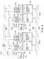
- FIG. 5 is a block diagram of another preferred embodiment of an EEPROM of the RWW specification having a redundant column cell array according to the present invention
- FIG. 6 is a block diagram of an address supply part in this preferred embodiment
- FIG. 7 is a block diagram. of another preferred embodiment of an EEPROM of the RWW specification having a redundant column cell array according to the present invention.
- FIG. 8 is a block diagram of another preferred embodiment of an EEPROM of the RWW specification having a redundant column cell array according to the present invention.
- FIG. 9 is a block diagram of another preferred embodiment of an EEPROM of the RWW specification having a redundant column cell array according to the present invention.
- FIG. 10 is a diagram showing the replacement of a block with a redundant cell array block in the preferred embodiments of FIGS. 5 and 7;
- FIG. 11 is a diagram showing the replacement of a block with a redundant cell array block in the preferred embodiment of FIG. 8;
- FIG. 12 is a diagram showing the replacement of a block with a redundant cell array block in the preferred embodiment of FIG. 9;
- FIG. 13 is a diagram showing the replacement of a block with a redundant cell array block in a modified preferred embodiment of the preferred embodiments of FIGS. 5 and 7;
- FIG. 14 is a block diagram of a preferred embodiment of an EEPROM having a redundant row cell array according to the present invention.
- FIG. 15 is a block diagram of an address supply part in this preferred embodiment.
- FIG. 16 is a diagram showing the details of a principal part in this preferred embodiment.
- FIG. 17 is a diagram showing the construction of a row main decoder in this preferred embodiment.
- FIG. 18 is a diagram showing the construction of a word line selecting drive circuit in this preferred embodiment.
- FIG. 19 is a diagram showing the construction of a row main decoder of another preferred embodiment of an EEPROM having a redundant row cell array according to the present invention.
- FIG. 20 is a flow chart showing the first half of a sequence of an automatic data erase operation in the preferred embodiment having the row main decoder shown in FIG. 19;
- FIG. 21 is a flow chart showing the second half of the sequence
- FIG. 22 is a block diagram of another preferred embodiment of an EEPROM of the RWW specification having a redundant row cell array according to the present invention.
- FIG. 23 is a schematic diagram showing another preferred embodiment of a semiconductor memory according to the present invention.
- FIG. 24 is a block diagram of a ROM fuse circuit in this preferred embodiment.
- FIG. 25 is a diagram showing a die sort flow in this preferred embodiment, as compared with that in a conventional case
- FIG. 26 is a schematic diagram showing another preferred embodiment of a semiconductor memory according to the present invention.
- FIG. 27 is a diagram showing the construction of a latch for use in this preferred embodiment.
- FIG. 1 shows the construction of a first preferred embodiment of an EEPROM having a column redundant circuit according to the present invention.
- a memory cell array 101 comprises a plurality of bit lines BL, a plurality of word lines WL, and a plurality of memory cells MC, each of which is arranged at a corresponding one of the intersections of the bit and word lines, as shown in FIG. 2 .
- Each of the memory cells MC has a MOS transistor structure having a floating gate and a control gate stacked thereon, and is designed to nonvolatilisably store, as binary data, the difference in threshold due to the presence of charge injection into the floating gate.
- FIG. 2 shows an example of a NOR type EEPROM. Also in preferred embodiments which will be described later, the same memory cell array structure will be used.
- a positive voltage is applied to a selected bit line BL, and a higher positive voltage the n that applied to the bit line BL is applied to a selected word line WL, so that electrons are injected into a floating gate by the hot electron injection.
- the state that electrons are injected into the floating gate to raise the threshold is, e.g., data “0”.
- a data erase operation a range including continuous word lines WL is used as a block serving as the minimum unit for erase, and a negative voltage is applied to all of the word lines WL every block to emit the electrons of the floating gate to a substrate. The state that the electrons of the floating gate are thus emitted to lower the threshold voltage is e.g., data “1”.
- a row address and, a column address are decoded, via a pre-decoder 107 , by means of a row decoder 102 and a column decoder 103 , respectively.
- the word lines selection and bit line selection of the memory cell array 101 are carried out.
- the bit line data selected by the column decoder 103 are detected and amplified by means of a sense amplifier circuit 104 .
- the sense amplifier circuit 104 has the function of latching data acquired via a data buffer 113 from an input/output terminal.
- a 16-bit parallel read/write operation is intended to be carried out, and 16 sense amplifier circuits 104 are provided for 16 input/output terminals to carry out data transfer to 16 bit lines BL.
- the usual memory cell array 101 is provided with redundant column cell arrays 201 ( 201 a through 201 c ), including spare bit lines SBL corresponding to a plurality of columns (three columns in the shown embodiment) in order to replace defective bit lines therein.
- Redundant sense amplifier circuits 105 are connected to the redundant column cell arrays 201 , respectively.
- a sense amplifier switching circuit 114 is designed to select one of the redundant sense amplifier circuits 105 .
- each of data switching circuits 112 . is provided for switching the selected redundant sense amplifier circuit 105 to one of the 16 sense amplifier circuits 104 to connect it to a data input/output buffer 113 .
- data in the redundant column cell arrays 201 and the selected data in the memory cell array 101 are simultaneously read out, and when a defective column is selected, an output switching control for using one of the redundant sense amplifier circuits 105 , which is connected to one of the redundant column cell arrays 201 , in place of the sense amplifier circuit 104 corresponding to the BMWs column is carried out.
- an output switching control for using one of the redundant sense amplifier circuits 105 which is connected to one of the redundant column cell arrays 201 , in place of the sense amplifier circuit 104 corresponding to the BMWs column is carried out.
- a defective address storing circuit 108 there are provided.
- the defective address storing circuit 108 is, e.g., a fuse circuit, and stores a defective column address which has been detected. by a test, data (4 bits in this preferred embodiment) for an input/output terminal, to and from which data corresponding to the detective column address should be inputted and outputted, and a set number (2 bits in this preferred embodiment) in a redundant column cell array 201 which corresponds to the input/output terminal and which should be substituted.
- the address comparator circuit 109 detects the coincidence of an input address with the defective address which has been held in the defective address storing circuit 108 .
- the detective IP) decoder 110 decodes an I/O terminal corresponding to the stored defective address on the basis of the detection signal, and outputs hit signals HIT ⁇ 0 : 15 >.
- the hit signals HIT ⁇ 0 : 15 > to mean a set of hit signals HIT ⁇ 0 > through HIT ⁇ 15 >.
- the sense amplifier switching circuit 114 By switching the sense amplifier switching circuit 114 in such a logic, it is possible to select one of the redundant sense amplifier circuits 105 .
- the logic of the block set number decoder 111 is set so that HIT ⁇ 15 > is 0-fixed at 00, this can be used as an enable bit.
- the sense amplifier circuit S/A (RD 0 ) of the redundant sense amplifier circuits 105 is selected.
- the output of this sense amplifier circuit S/A (RD 0 ) enters the data switch circuit 112 to be selected by the hit signal HIT ⁇ 5 > to be transferred to the data input/output buffer 113 .
- each of the redundant sense amplifier circuits 105 is provided for the corresponding one of the redundant column cell arrays 201 for three columns, and 16+3-bit data are simultaneously read out in a data read opertion. Then, the substitution for defective data corresponding to the defective address is carried out by the sense amplifier switching circuit 114 and the data switching circuits 122 .
- the redundant circuits for the plurality of columns are used, so that the relief efficiency is high.
- the output output of the redundant column cell array is read out simultaneously with the read-out of normal memory cell data including the defective address, and the read output of the defective column address is switched by the output of the redundant cell array.
- the read output of the redundant cell array is not delayed from the read output of the normal cell array.
- the outputs of. the plurality of redundant sense amplifier circuits 105 are switched by the sense amplifier circuit 114 to supply the output of one of the redundant sense amplifier circuits 105 to the data switching circuit 112 . That is, the outputs of the redundant sense amplifier circuits 105 are supplied to the data buffer 113 by means of the two-stage switching circuits of the sense amplifier switching circuit 114 and data switching circuits 112 Therefore, the number of buses between. the sense amplifier switching circuit 114 and the data switching circuits 112 can be one. That is, the number of buses between the sense amplifier switching circuit 114 and the data switching circuit 112 can be decreased as compared with when the sense amplifier switching circuit 114 is not provided.
- the number of the redundant columns should not be limited to three, but it may be more.
- the redundant sense amplifier circuits 105 may be provided for each of the redundant columns to use the circuit system in the above described preferred embodiment.
- FIGS. 3 and 4A show a preferred embodiment of an EEPROM of the RWW (Read While Write) specification having a column redundant circuit accord 1 ng to the present invention.
- a memory cell array is divided into at least two banks so that a data write or erase operation can be carried out in one bank while a data read operation is carried out in the other bank.
- a memory cell array 101 comprises two banks BANK 0 and BANK 1 .
- each of the banks BANK 0 and BANK 1 is provided with a pre-decoder 301 , a row decoder 302 and a column decoder 303 .
- each of the banks BANK 0 and BANK 1 is provided with a redundant column cell array 304 comprising a single spare bit line.
- two systems of address bus lines 305 a , 305 b and data bus lines 306 a , 306 b are provided commonly for the two banks.
- the address bus line 305 a is provided for carrying out a data read operation
- the address bus line 305 b is provided for carrying out a data write or erase operation
- the data bus line 306 a is provided for carrying out a data read operation
- the data bus line 306 b is provided for carrying out a data write or erase operation.
- a data write or erase command is inputted to a control circuit. 310 .
- a write address is received by an address latch 308 when a write command is inputted.
- an erase block address is set in at block selecting register (not shown) corresponding to a selected block when an a erase command is inputted.
- an address is supplied to the address bus line 305 a via an address buffer 307 .
- An address switching circuit 311 selects the address, which has been latched by the address latch 308 , in a data write operation, and the address, which is sequentially incremented from an address counter 309 , in a data erase operation, to supply the selected address to the address bus line 305 b.
- each of the banks BANK 0 and BANK 1 is provided with a busy, register 315 for indicating the operation mode of the selected bank.
- “H” is set in the busy register 315 by a command from the control circuit 310 .
- the busy register 315 holds “L”.
- Each of the banks BANK 0 and BANK 1 has a data line switching circuit (DLSW 1 ) 316 a for connecting the bank to the reading data bus line 306 a , and a data line switching circuit (DLSW 2 ) 316 b for connecting the bank to the writing or erasing data bus line 306 b .
- the 16-bit parallel read operation is carried out, so that the number of each of the data line switching circuits 316 a and 316 b is 16.
- two systems of data line switching circuits 317 a and 317 b are provided.
- the on-off of these two systems of data line switching circuits is controlled by data of the busy register 315 . That is, if the output of the busy register 315 has “H”, the data line switching circuits 316 b and 317 b are turned on, so that the bank is connected to the writing or erasing data bus line 306 b . If the output of the busy register 315 has “L”, the date line switching circuits 316 a and 317 a are turned on, so that the bank is connected to the writing or erasing data bus line 306 a.
- each of the banks is provided with two systems of address line switching circuits (AddSW 1 , AddSW 2 ) 318 a and 318 b .
- These address line switching circuits 318 a and 318 b are also controlled by the busy register 315 . That is, if the output of the busy register 315 has “H”, the address line switching circuit 318 b is turned on, so that the address of the writing or erasing address bus line 305 b is supplied to the pre-decoder 301 . If the output of the busy register 315 has “L”, the address line switching circuit 318 a , is turned on, so that the address of the reading address bus line 305 a is supplied to the pre-decoder 301 .
- Sense amplifier circuits 319 a for sensing read data are connected to the reading data bus line 306 a .
- Sense amplifier circuits 319 b for use in a verify read in a writing or erasing operation are connected to the writing or erasing data bus line 306 b .
- the 16-bit parallel operation is carried out, so that the number of each of the sense amplifier circuits 319 a and 319 b is 16.
- each of the data bus line 306 a and 306 b is provided with a single redundant sense amplifier circuit 320 a or 320 b.
- a data switching circuit 321 a is provided in order to replace one of the outputs of the sense amplifier circuits 319 a with the output of the redundant sense amplifier circuit 320 a when a defective column address is selected in a data read operation.
- This data switching circuit 321 a is controlled by a bit signal HITa ⁇ 0 : 15 > generated by the detection of a defective address.
- a data switching circuit 321 b is provided in order to replace one of the outputs of the sense amplifier circuits 319 b with the output of the redundant sense amplifier circuit 320 b when a defective column address is selected in a verify read operation.
- This data switching circuit 321 b is controlled by a bit signal HITb ⁇ 0 : 15 > generated by the detection of a defective address.
- read data are outputted to the outside via a data buffer 323 .
- read data in the verify read operation are fed to a determining circuit 322 , in which a verify determination is carried out.
- address comparator circuits 313 a , 313 b and defective I/O decoders 314 a , 314 b are provided so as to correspond to the two systems of address bus lines 305 a and 305 b .
- the defective column address of each of the banks, and data of an input/output terminal (I/O) corresponding thereto are stored in an address storing circuit 312 .
- Each of the address comparator circuits 313 a and 313 b detects the incidence of the address of the address bus lines 305 a and 305 b with the address, which has been held by the storing circuit 312 , in a data read operation and a verify read operation. After the coincidence is detected, hit signals HITa ⁇ 0 : 15 > and HITb ⁇ 0 : 15 > are outputted in accordance With a defective I/O by means of the defective I/O decoders 314 a and 314 b similar to the preceding preferred embodiment.
- an address acquired from the address buffer 307 is compared with the address of the defective address, storing circuit 312 in the address comparator circuit 313 a . If no coincidence is detected, all of hit signals HITa ⁇ 0 : 15 > have “0”. Therefore, all of the data switching circuits 321 a select the output of the sense amplifier circuit 319 a , so that the output of the sense amplifier circuit 319 a , is inputted directly to the data buffer 323 .
- the hit signal HITa ⁇ 0 > through the hit signal HITa ⁇ 14 > of the hit signals HITa ⁇ 0 : 15 > have “0”, and the hit signal HITa ⁇ 15 > thereof has “1”.
- an address from the address latch 308 or the address counter 309 is compared with the address of the defective address storing circuit 312 , in the address comparator circuit 313 b . If no coincidence is detected, all of the hit signals HITb ⁇ 0 : 15 > have “0”. Therefore, all of the data switching circuits 321 b select the output of the sense amplifier circuit 319 b , so that the output of the sense amplifier circuit 319 b is inputted directly to the determining circuit 322 .
- the hit signal HITb ⁇ 0 > through the hit signal HITb ⁇ 14 > of the hit signals HITb ⁇ 0 : 15 > have “0”, and the hit signal HITb ⁇ 15 > thereof has “1”.
- the two systems of address bus lines and data bus lines are provided commonly for the plurality of banks, and the connections of these two systems of address bus lines and data bus lines are switched by a busy signal, so that a data write or erase operation can be carried out in one bank while a data read operation can be carried out in the other bank.
- the output of the redundant column cell array is outputted to the redundant sense amplifier circuit simultaneously with the output of the original memory cell array.
- two systems of address comparator circuits for detecting the coincidence of the defective address are prepared so as to correspond to the operation modes of two system, and the output of the sense amplifier circuit is switched in each of the operation modes to realize the substitution for a defective column.
- one redundant column cell array 304 has been provided for simple explanation.
- a plurality of redundant column cell arrays may be prepared to carry out the substitution for a plurality of columns by the same system as that in the first preferred embodiment.
- FIGS. 4B and 4C show the construction of an EEPROM then one memory cell array 101 is provided with three redundant column cell arrays 304 a through 304 c in the second preferred embodiment, which correspond to FIGS. 3 and 4A, respectively.
- each of the data line switch circuits 317 a is connected to the data reading data bus line 306 a
- each of the data line switching circuits 317 b is connected to the data writing or erasing data bus line 306 b.
- the three redundant sense amplifier circuits 324 a through 324 c are connected to the data reading the bus line 306 a . These three redundant sense amplifier circuits 324 a through 324 c detect and amplify the read data of the three redundant column cell arrays 304 a through 304 c , respectively. These three redundant sense amplifier circuits 324 a through 324 c are connected to the sense amplifier switching circuit 114 a via three data bus lines. Moreover, the sense amplifier switching circuit 114 a is connected to each of the data switching circuits 321 a in the wiring form that one data bus line finally branches.
- This sense amplifier switching circuit 114 a is a circuit for connecting one of data bus lines from the redundant some amplifier circuits 324 a through 324 c to the data switching circuit 321 a on the basis of a logic signal LGCa outputted from the block set number decoder 111 a (see FIG. 4 C).
- three redundant sense amplifier circuits 325 a through 320 are connected to the writing or erasing data bus line 306 b . These three redundant sense amplifier circuits 325 a through 325 c detect and amplify the verify read data of the three redundant column cell arrays 304 a through 304 c , respectively. These three redundant sense amplifier circuits 325 a through 325 c are connected to the sense amplifier switching circuit 114 b via three data bus lines. Moreover, the sense amplifier switching circuit 114 b is connected to each of the data switching circuits 321 b in the wiring form that one data bus finally branches.
- This sense amplifier switching circuit 114 b is a circuit for connecting one of the data bus lines from the redundant sense amplifier circuits 324 a through 324 c to the data switching circuit 321 b on the basis of a logic signal LGCb outputted from the block set number decoder 111 b (see FIG. 4 C).
- FIGS. 5 and 6 show a preferred embodiment of an EEPROM of the RWW specification of a block redundant circuit system wherein a block which is the minimum unit for data, erase in the memory cell many and which is a set of a plurality of memory cells corresponds to a unit for substitution for defect relief.
- a memory cell array 401 basically has the same construction as those in the first and second preferred embodiments, except that it is divided into at least two banks BANK 0 and BANK 1 similar to the second preferred embodiment.
- a redundant cell array block (which will be hereinafter simply referred. to as a redundant block) 403 is provided.
- the redundant block 403 comprises one spare block or a plurality of spare blocks.
- the memory cell array 401 and the redundant block 403 include a row decoder, a column decoder and a sense amplifier circuit. As memory cell array 401 and the redundant block 403 are provided with pre-decoders 402 and 404 for decoding a row address and column address supplied thereto, respectively.
- each of the banks BANK 0 and BANK 1 is provided with a busy register 315 and with address line switching circuits 318 a and 318 b which are on-off controlled by the busy register 315 . That is, in a write or erase mode, the address of the address bus line 305 b is simultaneously supplied to the pre-decoders 402 and 404 by the address line switch circuit 318 b . In a read mode, the address of the address bus line 305 a is simultaneously supplied to the pre-decoders 402 and 404 by the address line switching circuit 318 a.
- Each of the banks BANK 0 and BANK 1 is provided with two systems of high address switching circuits 4 l 0 a and 410 b .
- the hit address switching circuit 410 b also controls the activity and inactivity on the sides of the memory cell array 401 and redundant block 403 .
- the reading data bus line 306 a and the writing or erasing data bus line 306 b are provided commonly far each of the banks BANK 0 and BANK 1 .
- addresses have been simultaneously supplied to the memory cell array 401 and the redundant block 403 , when an input address is not coincident with the defective address, the side of the memory cell array 401 is active, and when the input address hits the defective address, the side of the redundant block 403 is active, so that data are read out therefrom.
- These read data are switched to the reading data bus line 306 a or the verify reading data bus line 306 b in accordance with the operation mode to be outputted.
- control of the substitution for a defective address every block in a bank, in which a data read operation is being carried out is independent of that in a bank, in which a data write or erase operation is being carried out.
- the replacement of a block with a redundant block 403 is carried out only within a bank, to which the redundant block belongs.
- FIG. 7 shows a preferred embodiment as the a modification of the third preferred embodiment.
- each of the banks BANK 0 and BANK 1 is provided with core decoders 420 a and 420 b for selecting a core in the bank, so as to correspond to two systems of address bus lines 305 a and 305 b .
- the “core” is herein a set of a plurality of blocks, each of which is the minimum unit for data erase. For example, eight blocks constitute one core.
- the bank comprises one core or a plurality of cores.
- the core decoders 420 a and 420 b are supplied to the pre-decoder 402 on the side of the memory cell array 401 and to the pre-decoder 404 on the side of the redundant block 403 via core switching circuits 421 a and 421 b which are selectively on-off controlled by the busy register 315 . That is, in the bank wherein the output of the busy register 315 has “H”, the core address of the address bus line 305 b is decoded by the cane decoder 420 b to be supplied to the pre-decoder 402 and 404 via the core switching circuit 421 b .
- the pre-decoders 402 and 404 are selectively active and inactive by the bit signal HITb is the same as that in the preceding third preferred embodiment.
- the CORE address of the address bus line 305 a is decoded by the CORE decoder 420 a to be supplied to the pre-decoders 402 and 404 via the core switching circuit 421 a .
- the pre-decoders 402 and 404 are selectively active and inactive in accordance with the bit signal HITa which is the result of the coincidence detection with the defective address.
- the control of the substitution for a defective address every block in a bank, in which a data read operation is being carried out is independent of that in a bank, in which a data write or erase operation, is being carried out.
- the core decoders 420 a and 420 b for decoding core addresses are provided upstream of the pre-decoder 404 , so that the number of switches of the address line switching circuits 318 a and 318 b can be less than that in the preceding third preferred embodiment.
- FIG. 10 is a conceptual diagram showing the state of the defective block substitution in the third or fourth preferred embodiment of an RWW type EEPROM. While the description of the relationship between power supplies has been omitted above, separate power supply lines 432 a and 432 b , which are connected to a reading power supply 431 a and a writing or erasing power supply 431 b , respectively, are provided commonly for the tanks BANK 0 and BANK 1 as shown in this figure in order to meet the RWW specification. In accordance with the operation mode of each of the banks, these power supply lines 432 a and 432 b , are selected by power supply line switching circuits 433 and 434 to be connected to each of the banks BANK 0 and BANK 1 .
- FIG. 10 also shows the case where one bank BANK 0 has a large capacity and comprises a plurality of cores 0 through n, and the other bank BANK 1 comprises a single core.
- Eight blocks BLK 0 through BLK 7 are prepared for each block as normal blocks, and each core is provided with a spare block RBLK having a common core address.
- This spare block RBLK constitutes the above described redundant block 403 .
- the block substitution range is not only limited to the same bank, but it is also limited to the same core. In other words, if a defect exists in a certain core, it is only possible to replace with a spare block having a core address common to that of the core.
- FIG. 8 is a preferred embodiment wherein the preferred embodiment shown in FIG. 7 is modified to increase the degree of freedom for the block substitution.
- hit signals HITa and HITb enter core decoders 420 a and 420 b .
- the hit signals HITa and HITb include a core address of a core including a spare block to be substituted, as well as an address coincidence detection signal.
- the defective address storing circuit 312 shown in FIG. 6 has stored therein the core address of the spare block to be substituted for the block of the defective block address, as well as the defective block address.
- the address comparator circuits 313 a and 313 b output the hit signals HITa and HITb including a core address, to which the spare block to be substituted belongs, while outputting the coincidence detection signal of the defective address, to feed dose signals to the core decoders 420 a and 420 b .
- the core decoder 420 a and 420 b decode the core address, which is assigned when the defective address is detected, to select the spare block.
- FIG. 11 shows the state of the block substitution in this preferred embodiment which corresponds to FIG. 10 .
- the defective block BLK 7 can not only be replaced with the spare block RBLK belonging to core 1 , but it can also be replaced with the spare block RBLK of core 0 .
- the degree of freedom for the defective block substitution can be further increased to realize a high relief efficiency.
- FIG. 9 shows a preferred embodiment wherein the restrictions on the block substitution, which should be carried out within the limits of the bank, are removed to further enhance the degree of freedom for the block substitution.
- a redundant block 403 is provided independently of the memory cell arrays 401 of the banks BANK 0 and BANK 1 .
- the fact that the redundant block 403 is independent of the banks BANK 0 and BANK 1 means that an address is supplied only when a defective address is detected independently of the decoding circuits of the memory cell arrays 401 of the banks BANK 0 and BANK 1 .
- the redundant block 403 is also provided with address line switching circuits 501 a and 501 b for switching two systems of address lines 305 a and 305 b .
- each of the banks BANK 0 and BANK 1 is provided with core decoders 420 a and 420 b which correspond to the two systems of address bus lines 305 a and 305 b , respectively, and the redundant block 403 is also provided with core decoders 502 a and 502 b which correspond to the address bus lines 305 a and 305 b , respectively.
- Hit signals HITa and HITb obtained in output signal lines 411 a and 411 b of two system of address comparator circuits 313 a and 313 b are inverted to enter, as activated signals, the core decoders 420 a and 420 b of each of the banks BANK 0 and BANK 1 .
- the hit signals HITa and HITb obtained in the output signal lines 411 a and 411 b directly enter, as activated signals, the core decoders 502 a and 502 b an the side of the redundant block 403 .
- one address line switching circuit 501 a is turned on by the output of the core decoder 502 a
- the other address line switching circuit 501 b is turned on by the output of the core decoder 502 b .
- the defective address storing circuit 312 stores therein an address of a spare block to be substituted, as well as a defective block, and outputs the address of the spare block while outputting a coincidence detection signal.
- the disjunction of the outputs of the core decoders 502 a and 502 b is derived by an OR gate G to be used as a core selecting signal to control the activity and inactivity of the pre-decoder 404 on the side of the redundant block 403 .
- the core decoders 420 a and 420 b of each of the banks BANK 0 and BANK 1 are active, and an access corresponding to the operation mode with respect to each of the banks BANK 0 and BANK 1 is obtained in accordance with the output of the busy register 315 .
- the core decoders 420 a and 420 b of each of the banks BANK 0 and BANK 1 are inactive, but the core decoders 502 a and 502 b on the side of the redundant block 403 are active. Then, in accordance with the operation mode, an access to the redundant block 403 is obtained by the addresses of the address signal lines 305 a and 305 b , so that a specific spare block is selected.
- the redundant block 403 can be substituted for defective blocks of either of the banks BANK 0 and BANK 1 .
- the state of the block substitution in this preferred embodiment is conceptually shown in FIG. 12 .
- one spare block RBLK 1 of the redundant block 403 is substituted for the defective block BLK 7 in core n of the bank BANK 0
- other spare blocks RBLK 2 and RBLK 3 are substituted for the blocks BLK 6 and BLK 7 in the bank BANK 1 respectively.
- the block substitution can be carried out without the restrictions on the bank to enhance the degree of freedom for substitution and the relief efficiency.
- each of the spare blocks is provided with a power supply switching circuit 503 .
- the bank BANK 0 is in a data read mode and if a block substitution is carried out in the bank, it is required to connect the reading power supply line 432 a to the spare block.
- FIGS. 10 and 11 show the case where the capacities of the banks BANK 0 ) and BANK 1 are different, and spare blocks are arranged in accordance with the capacities.
- the number of spare blocks on the side of the bank BANK 1 having a smaller capacity is naturally smaller. Therefore, if the substitution range is limited to the range of the bank, it is not possible to replace a large number of blocks in the bank having the smaller capacity.
- FIG. 13 shows a preferred embodiment, taking account of this point so as to correspond to FIG. 11 .
- the bank BANK 0 one spare block RBLK is arranged with respect to one core, whereas in the bank BANK 1 comprising one core, two spare blocks are arranged.
- the substitution efficiency in the bank BANK 1 having the smaller capacity can be increased.
- the capacity ratio of the spare block in the bank having the smaller capacity to the memory cell array is set to be greater than the capacity ratio of the spare block in the bank having the larger capacity to the memory cell array.
- main word lines continuously extending aver a plurality of blocks in the row directions of a memory cell array are provided, and each of the blocks is provided with separate word lines.
- One of the main word lines is selected by a row main decoder, and word lines of a plurality of blocks along the selected main word line are selected by a row sub-decoder.
- Such a decode system is called a two-stage decode system which is described in, e. g. , Japanese Patent Application No. H11-73226 which has not been publicly known and which has been individually known by the inventor.
- the substitution for a defective row is usually carried out every main word line.
- a defective row substitution can be carried out every block.
- the word lines of a defective row and the word lines of unselected blocks can be set at 0 V to prevent useless pass current from flowing.
- FIG. 14 shows the constructions of a memory cell array 601 and a selecting drive circuit part of a row system thereof in this preferred embodiment.
- the memory cell array 601 shows one core portion comprising eight blocks BLK 0 through BLK 7 in row directions. Usually, one core or a plurality of cores, each of which is the same as the core portion, are arranged to constitute an EEPROM.
- main word lines Mi and MBi which continuously extend over the blocks BLK 0 and BLK 7 and which are complementary signal lines to each other, and word lines WL 0 and WL 7 for each block, which are selected by the main word lines Mi and MBi.
- a redundant row cell array 602 is arranged.
- the redundant row cell array 602 has one or more redundant main word lines.
- a row main decoder 603 selects one of the main word lines Mi and MBi of the memory cell array 601 , and each of row sub-decoders 604 ( 604 a , 604 b , . . . ), each of which is provided in a corresponding one of the blocks, selects one of the word lines WL in the corresponding one of the blocks on the basis of the selected main work line Mi or MBi.
- two row sub-decoders 604 are provided between adjacent two blocks. Specifically, as shown in FIG.
- each of the row sub-decoders 604 has a transfer gate, which comprises an NMOS transistor QN 1 and PMOS transistor QP 1 which are driven by the main word lines Mi and MBi, and an NMOS transistor QN 2 which is driven by the main word line MBi for resetting the word line WL at VSS.
- the row sub-decoder 604 is designed to transfer word line driving voltages BLKF 1 through BLKF 4 , which are generated from the word line selecting drive circuit 606 in accordance with the operation mode, to the word line WL of each block.
- the word line selecting drive circuit 606 comprises four drivers F 1 through F 4 common to every adjacent two blocks.
- transfer gates 608 ( 608 a , 608 b , . . . ) are provided between the row sub-decoder 604 and the word line selecting drive circuit 606 .
- Each of the transfer gates 608 is designed to selectively transfer the output of each of the drivers F 1 and F 4 of the word line selecting drive circuit 606 to the row sub-decoder 604 .
- Each of the transfer gates 608 comprises an NMOS transistor QN 3 and PMOS transistor QP 2 , which are controlled by complementary outputs BR and BRB (BRa and BRBa, BRb and BRBb, . . . ) of a block decoder 607 for decoding a block address, and an NMOS transistor QN 4 for resetting an input signal line to the row sub-decoder 604 at VSS.
- the output of an address buffer 610 for acquiring an external address in a data read operation, and the output of an address counter 611 for generating sequentially updated addresses in a data erase verify operation are switched by an address switching circuit 613 in accordance with the operation mode to be fed to a pre-decoder 615 , the word line selecting drive circuit 606 and the block decoder 607 .
- the pre-decoder 615 separates a row address and a column address from each other to supply the separated addresses to the main row decoder 603 and column decoder (not shown), respectively.
- the word line selecting drive circuit 606 receives a signal for simultaneously selecting eight blocks (e.g., a core selecting signal when one core comprises eight blocks) to generate a word line driving voltage.
- FIG. 14 the elements of the column system are omitted.
- a column decoder for carrying out a bit line selection similar to usual EEPROMs, and a sense amplifier circuit for detecting read data of a bit line selected by the column decoder and for latching write data.
- a defective address storing circuit 612 is designed to store therein a block address including a defective word line, as well as a defective row address.
- the pre-decoder 615 is deactivated, and the redundant row selecting circuit 605 is activated, so that the defective row is replaced by the redundant row cell array.
- the address switching circuit 613 is controlled by an erase mode control signal ERS, which is obtained from a control circuit, for acquiring the defective row address of the defective address storing circuit 612 and the block address.
- the pre-decoder 615 selects the defective row, and the row main decoder 603 is set so that only the defective row is “unselected” and other rows are “selected”.
- the block decoder 607 selects a block to be erased, and controls the transfer gate 608 .
- 0 V is applied to the defective word line
- a negative voltage VBB is applied to all of other word lines, although this will be described in detail later.
- all of word lines are controlled so as to have a voltage of 0 V regardless of the presence of selection of a main word line.
- the row main decoder 603 is formed as shown in FIG. 17.
- a NAND gate G 11 is a decoding gate for selecting a main word line.
- the signal of the node N 12 is inverted by a clocked inverter CI 1 to be transferred.
- the signal of the node N 1 together with the signal inverted by an inverter I 1 , is inputted to a level shifter LS 1 to be converted into a signal for applying “H” level to a positive booster circuit output VSW and “L” level to VSS (ground). Moreover, the output thereof is converted into a signal for assigning “H” level to a voltage VSW and “L” level to a negative booster circuit output VBB, by means of a level shifter LS 2 . Then, the output of the level shifter LS 2 is supplied to one main word line MBi via inverters I 2 , I 3 and I 4 , and the output of the inverter I 2 is inverted by an inverter I 5 to be supplied to the other main word line Mi.
- the row main decoder part for the redundant row cell array 602 receives only the hit signal HIT, which is outputted by the coincidence detection with the defective address in the address comparator circuit 613 , the block address and VSS, in place of inputs GAi, GBi, GCi, and the construction thereof is the same.
- the word line selecting drive circuit 606 is formed as shown in FIG. 18 .
- the NAND gate G 21 of each of the driver F 1 through F 4 is a decoding gate for selecting one set of four sets of row sub-decoders 604 for eight blocks, and the output thereof has “L” in a selected state.
- the output of the NAND gate G 21 passes through two stages of NAND gates G 22 , G 23 , two stages of level shifters LS 3 , LS 4 and inverters I 8 through I 10 to generate a word line driving signal BLK.
- the erase control signal ERS “H”.
- the transfer gate TG 2 is turned OFF, and the clocked inverter CI 2 is turned ON. Therefore, “L” enters the NAND gate G 22 , and the core selecting signal Bi is inverted by the clocked inverter CI 2 to be inputted to the NAND gate G 23 .
- the output node N 3 of the NAND gate G 23 has an inverse logic to data read and write, and has “H” in the selected state.
- the word line driving signals BLKF 1 through BLKF 4 are transferred to the row sub-decoder 604 via the transfer gate 608 which is selected by the block decoder 607 .
- a driving voltage BLKF is applied to the selected word line WL in accordance with the potentials of the main word lines Mi and MBi.
- the transfer gate of the row sub-decoder 604 a is turned on, and the word line driving signal BLKF 1 is transferred to the word line via the transfer gate 608 a , so that the word line has a negative voltage VBB.
- a block erase operation is carried out without applying the negative voltage VBB to the defective word line. Therefore, useless pass current does not flow due to the application of the negative voltage VBB to the defective word line.
- the transfer gates 608 b , 608 c , . . . are turned off, so that all of the word lines are set so as to have VSS regardless of the main word lines Mi and MBi.
- any useless pass current paths from the booster circuit are not formed even if defects exists at different addresses every block.
- the block address, together with the row address, as defective address information it is possible to replace defective word lines having different addresses every block. Thus, it is possible to obtain a high relief efficiency.
- the eighth preferred embodiment uses the decode system wherein, in the data erase operation, the defective address held in the defective address storing circuit is decoded by the main row decoder as the internal address to set the defective row in the “unselected” state. Therefore, the redundant row cell array can be substituted for one set (four word lines) in one block.
- the main row decoder 603 in the eight preferred embodiment is modified as shown in FIG. 19 .
- the output node N 1 of each decoding NAND gate G 11 is provided with a NOR gage G 31 controlled by a row selecting signal SELB, and there is a latch circuit (register) LCC comprising NOR gates G 32 and G 33 for acquiring selection information from the output of the NOR gate G 31 .
- the output of the latch circuit LCC enters a clocked inverter CI 1 .
- timing in setting data in the latch circuit LCC of the row main decoder 603 should not be limited to that in the write operation before the data erase operation. If there is a sequence of updating all of row addresses before a data erase operation, the setting of data in the latch circuit LCC of the row main decoder 603 can be carried out in the sequence.
- FIGS. 20 and 21 show an automatic data erase sequence in the ninth preferred embodiment of an EEPROM according to the present invention.
- FIG. 20 shows a data write cycle before a data erase operation.
- initial conditions are set (S 1 )
- a write verify is set up (S 2 )
- a write verify read operation if carried out (S 3 ).
- LCC of the row main register of a row address selected by the verify read operation “1” being row selecting information is set (S 4 ).
- a verify determination for determining whether the write state is within a threshold range is carried out (S 5 ).
- step S 5 the cycle is initialized (S 10 ), and it is determined whether the address reaches the final address (S 11 ). If the address does not reach the final address, the address is updated (S 12 ), and the next address write and verify operations are repeated. If the address reaches the final address, the routine goes to a data erase flow shown in FIG. 21 . First, an erase verify is set up (S 21 ), a verify read operation is carried out (S 22 ), and it is determined whether the erase state is within a predetermined threshold range (S 23 ). If the determined result is NG, a cycle limit determination is carried out (S 24 ).
- the cycle is initialized (S 28 ), and it is determined whether the address reached the final address (S 29 ). If the address does not reach the final address, the address is updated (S 30 ), and the next address erase and verify operations are repeated. If the address reaches the final address, read conditions are set up (S 31 ), and the routine ends.
- the automatic erase sequence in the eighth preferred embodiment is the same as that shown in FIGS. 20 and 21, except that step S 4 in FIG. 20 is not provided.
- FIG. 22 shows the whole construction of a preferred embodiment of an EEPROM of the RWW specification having a redundant row cell array according to the present invention.
- This figure shows the case where a memory cell array 701 is divided into two banks BANK 0 and BANK 1 to make it possible to carry out a data write or erase operation in one of the banks while carrying out a data read operation in the other bank.
- a redundant row cell array 703 is provided for the memory cell array 701 of each of the banks BANK 0 and BANK 1 . Similar to the third preferred embodiment, the memory cell array 701 and the redundant row cell array 703 are provided with pre-decoders 702 and 703 , respectively.
- a reading address bus line 305 a and a writing or erasing address bus line 305 are provided in parallel, that two systems of address comparator circuits 313 a and 313 b are provided so as to correspond thereto, that two systems of address switching circuits 318 a , 318 b and hit address line switching circuits 410 a , 410 b are provided, a busy register 315 is provided for setting one of the banks BANK 0 and BANK 1 in a data write or erase mode in response to a control signal from a control circuit 310 , are the same as those in e.g., the preceding third preferred embodiment.
- the difference between this preferred embodiment and the third preferred embodiment or the like is that the defective address of the defective address storing circuit 312 is acquired and decoded as an internal address by an address switching circuit 311 in a data erase operation.
- the relief of a defective row in a bank which is in a write or erase mode can be independent of that in a bank which is in a read mode.
- a fuse circuit is used as the defective address storing circuit.
- the fuse circuits include a metal fuse circuit for fixedly storing data by mechanical cutting, and an electrically rewritable ROM fuse using nonvolatile memory cells.
- the ROM fuse circuit can be used for replacement of a defective address in the die sort process, the circuit is complicated and requires a large area.
- the metal fuse circuit can have a small area, the circuit can no be used for replacement of a defective address in the die sort process. Therefore, if the area penalty causes a serious problem as the increase of memory capacity, the metal fuse circuit is effective.
- the production of the metal fuse circuit requires a fuse blow process for programming. This must be carried out by taking out a wafer (or chip) from a die sort system. For example, in order to substitute a redundant cell array for a defective address which is found in a certain die sort process, the wafer must be taken out from the die sort system. Then, it is required to carry out a fuse blow to put the wafer in the die sort system again to carry out a die sort. Therefore, in order to inspect many wafers, it is required to provide a fuse blow process every die sort, so that the total die sort time increases.
- FIG. 23 shows the schematic chip construction of a preferred embodiment of a semiconductor memory according to the present invention, which can shorten the total die sort time in view of the foregoing. Furthermore, this preferred embodiment can not only be applied to any one of the preceding preferred embodiments of an EEPROM according to the present invention, but it can also be applied to any one of other semiconductor memories, such as DRAMs and SRAMs.
- FIG. 23 shows only a circuit part required to substitute a redundant cell array 831 for a body cell array 830 in a memory chip.
- a defective address storing circuit 800 There are provided a defective address storing circuit 800 , an address comparator circuit 803 for detecting the coincidence of an input address with a defective address stored in the defective address storing circuit 800 , and a control circuit 804 for carrying out an address substitution control by a coincident detection output.
- the defective address storing circuit 800 has a ROM fuse circuit 802 in addition to an aluminum fuse circuit 801 using an aluminum fuse as a metal fuse.
- the aluminum fuse circuit 801 is designed to fixedly store a defective address by mechanical cutting due to the fuse blow.
- the ROM fuse circuit 802 can rewrite data and erase data, the ROM fuse circuit 802 is usable not only as a circuit for fixedly storing a defective address, but also as a temporary storage circuit for temporarily writing and holding a defective address found by the die sort.
- the ROM fuse circuit 802 has a capacity sufficient for storing a suitable plurality of addresses. The write/erase operation of this ROM fuse circuit 802 can be carried out by the control circuit 804 while holding the wafer (or chip) in the die sort system.
- the ROM fuse circuit 802 has a ROM fuse array 811 comprising electrically rewritable nonvolatile memory cells MC which are the same as the memory cells of the body cell array 830 . Since the capacity of the ROM fuse array 811 is far smaller than that of the body cell array 830 , dummy cells for insuring the regularity of the pattern are arranged so as to obtain the same processing conditions as those for the body cell array 830 .
- a bias circuit 813 for generating a high voltage or the like is provided.
- a switching circuit 812 including a selecting gate and a write load is provided. The defective address selected by the switching circuit 812 is outputted via a buffer circuit 814 .
- FIG. 25 ( b ) shows a conventional case where a defective address storing circuit consists of a fuse circuit.
- a defective address found herein is stored in the defective address storing circuit by taking out a wafer (or chip) from a die sort system to carry out a fuse blow. Then, the wafer (or chip) is put in the die sort system again to carry out a die sort B. After the die sort B ends, a defective address sound herein is stored in the defective address storing circuit by taking out the wafer (or chip) from the die sort system to carry out a fuse blow. Then, the same operation is repeated.
- FIG. 25 ( a ) shows a preferred embodiment wherein a ROM fuse circuit 802 is provided.
- a defective address found herein is temporarily written to the ROM fuse circuit 802 and replaced. If the replacement of a defective address in a block address to be tested by using the ROM fuse circuit 802 is performed, it is possible to perform tests assuming that the defective address has been replaced by using the aluminum fuse circuit 801 . Since this defective address write operation can be carried out by inputting an electric signal from the outside, the operation can be carried out while the wafer (or chip) is put in the die sort system. However, the defective address is stored in a fail memory in tester at any time.
- the ROM fuse circuit 802 Because it is difficult to store all the defective addresses in the ROM fuse circuit 802 in view of capacity thereof. Therefore, only the defective address in a block to be tested is replaced by using the ROM fuse circuit 802 . Then, the ROM fuse circuit 802 and the address comparator circuit 803 carry out the substitution control of the defective address to carry out the next die sort B. The defective address found by the die sort B is also temporarily written and held in the ROM fuse circuit 800 and the test process proceed temporarily replacing.
- FIG. 25 ( a ) shows an example where the defective addresses temporarily held in the die sorts A through C are batch-transferred to the aluminum fuse circuit 801 to carry out a fuse blow after the die sort C is carried out. That is, at this stage, the wafer (or chip) is taken out from the die sort system, and the defective addresses held in the fail memory in tester and/or the ROM fuse circuit 802 are read out to carry out the fuse blow of the defective address. Thereafter, the ROM fuse circuit 802 is reset, and a die sort is carried out in the same sequence.
- the fuse blows can be simultaneously carried out after the plurality of die sorts, so that it is possible to reduce the number of fuse blow processes. Since the wafer (or chip) must be taken out from the die sort system in order to carry out the fuse blow, the reduction of the number of fuse blow processes can greatly shorten the total die sort time.
- FIG. 26 shows a preferred embodiment where a latch circuit 821 is substituted for the ROM fuse circuit 802 in the preferred embodiment shown in FIG. 23 .
- the latch circuit 821 comprises well-known latches which are shown in FIG. 27 and the number of which is sufficient to store required address information.
- the defective address held in the latch circuit 821 and the address held in the aluminum fuse circuit 801 are designed to be selectively fed to the defective address comparator circuit 803 by means of a switch 822 .
- the die sort flow in this preferred embodiment is the same as that in FIG. 25 ( a ), and the defective address found in the die sort A is temporarily stored in the latch circuit 821 and also stored in the fail memory in the tester. Furthermore, by replacing the defective address in the block to be tested by using the latch circuit 821 , it is possible to test assuming that the defective address has been replaced by using the aluminum fuse circuit 801 . In the next die sort B, the switch 822 is controlled so that the defective address held in the latch circuit 821 enters the comparator circuit 803 . Thus, the defective address found in the die sort A is replaced to carry out the die sort B. Then, the defective addresses held in the latch circuit 821 by a plurality or all of dies sorts are simultaneously written in the fuse circuit 801 .
- the total die sort time can be shortened due to the reduction of the number of fuse blow processes.
- the data of the latch circuit is volatile, there are advantages in that the latch circuit does not require any circuit parts required to control write/erase unlike the ROM fuse circuit 802 , and has a simple circuit construction and a small area penalty.
- the latch circuit can be utilized for uses other than the temporary holding of the defective addresses.
- the redundant sense amplifier circuit is provided for each of the redundant column cell arrays of the plurality of columns.
- normal cell array data and redundant cell array data are designed to be simultaneously read out in a data read operation, so that the sense amplifier switching circuit and the data switching circuit carry out the replacement of defective data corresponding to a defective address.
- this system is effectively applied to an EEPROM of the RWW specification wherein address bus lines and data bus lines are provided commonly for a plurality of banks.
- the redundant cell array block is arranged in each of banks, so that it is possible to obtain an EEPROM of the RWW specification wherein the control of the substitution for defective address every block in a bank, in which a data read operation is being carried out, is independent of that in a bank, in which a data write or erase operation is being carried out.
- the redundant row cell array is provided.
- 0 V is applied to defective word lines and a negative voltage is applied to other word lines.
Landscapes
- Engineering & Computer Science (AREA)
- Microelectronics & Electronic Packaging (AREA)
- For Increasing The Reliability Of Semiconductor Memories (AREA)
- Read Only Memory (AREA)
Priority Applications (1)
| Application Number | Priority Date | Filing Date | Title |
|---|---|---|---|
| US09/963,404 US6532181B2 (en) | 1999-06-03 | 2001-09-27 | Semiconductor memory device having redundant circuitry for replacing defective memory cell |
Applications Claiming Priority (4)
| Application Number | Priority Date | Filing Date | Title |
|---|---|---|---|
| JP15625599 | 1999-06-03 | ||
| JP11-156255 | 1999-06-03 | ||
| JP2000065398A JP2001052495A (ja) | 1999-06-03 | 2000-03-09 | 半導体メモリ |
| JP12-065398 | 2000-03-09 |
Related Child Applications (1)
| Application Number | Title | Priority Date | Filing Date |
|---|---|---|---|
| US09/963,404 Continuation US6532181B2 (en) | 1999-06-03 | 2001-09-27 | Semiconductor memory device having redundant circuitry for replacing defective memory cell |
Publications (1)
| Publication Number | Publication Date |
|---|---|
| US6320800B1 true US6320800B1 (en) | 2001-11-20 |
Family
ID=26484060
Family Applications (2)
| Application Number | Title | Priority Date | Filing Date |
|---|---|---|---|
| US09/583,540 Expired - Lifetime US6320800B1 (en) | 1999-06-03 | 2000-06-01 | Semiconductor memory and nonvolatile semiconductor memory having redundant circuitry for replacing defective memory cell |
| US09/963,404 Expired - Lifetime US6532181B2 (en) | 1999-06-03 | 2001-09-27 | Semiconductor memory device having redundant circuitry for replacing defective memory cell |
Family Applications After (1)
| Application Number | Title | Priority Date | Filing Date |
|---|---|---|---|
| US09/963,404 Expired - Lifetime US6532181B2 (en) | 1999-06-03 | 2001-09-27 | Semiconductor memory device having redundant circuitry for replacing defective memory cell |
Country Status (5)
| Country | Link |
|---|---|
| US (2) | US6320800B1 (ko) |
| EP (1) | EP1058192B1 (ko) |
| JP (1) | JP2001052495A (ko) |
| KR (1) | KR100351596B1 (ko) |
| DE (1) | DE60035736T2 (ko) |
Cited By (27)
| Publication number | Priority date | Publication date | Assignee | Title |
|---|---|---|---|---|
| US6496427B2 (en) * | 2000-08-28 | 2002-12-17 | Matsushita Electric Industrial Co., Ltd. | Nonvolatile semiconductor memory device |
| WO2002101749A1 (en) * | 2001-06-08 | 2002-12-19 | Mitsubishi Electric Corporation | Methods and apparatus for analyzing and repairing memory |
| US6504744B2 (en) * | 2000-06-09 | 2003-01-07 | Mitsubishi Denki Kabushiki Kaisha | Semiconductor memory device with memory test circuit |
| US6535438B2 (en) * | 2001-03-21 | 2003-03-18 | Mitsubishi Denki Kabushiki Kaisha | Semiconductor memory device adopting redundancy system |
| US6552935B2 (en) | 2001-08-02 | 2003-04-22 | Stmicroelectronics, Inc. | Dual bank flash memory device and method |
| US6553449B1 (en) * | 2000-09-29 | 2003-04-22 | Intel Corporation | System and method for providing concurrent row and column commands |
| US20030084386A1 (en) * | 2001-10-25 | 2003-05-01 | Barth John E. | ECC Based system and method for repairing failed memory elements |
| US6563732B2 (en) * | 2001-08-02 | 2003-05-13 | Stmicroelectronics, Inc. | Redundancy circuit and method for flash memory devices |
| US20030107926A1 (en) * | 2001-10-12 | 2003-06-12 | Mitsubishi Denki Kabushiki Kaisha | Semiconductor device provided with memory chips |
| US20030117867A1 (en) * | 2001-12-14 | 2003-06-26 | Tadayuki Taura | Semiconductor memory device |
| US6594177B2 (en) * | 2001-08-02 | 2003-07-15 | Stmicroelectronics, Inc. | Redundancy circuit and method for replacing defective memory cells in a flash memory device |
| US20040066684A1 (en) * | 2002-10-08 | 2004-04-08 | Hiroshi Ito | Semiconductor integrated circuit device |
| US20040085819A1 (en) * | 2001-12-26 | 2004-05-06 | Tokumasa Hara | Semiconductor integrated circuit device and read start trigger signal generating method therefor |
| US20040120202A1 (en) * | 2001-02-02 | 2004-06-24 | Esin Terzioglu | Block redundancy implementation in heirarchical RAM'S |
| US20040218328A1 (en) * | 2003-02-14 | 2004-11-04 | Naokazu Kuzuno | Fuse latch circuit |
| US20040233699A1 (en) * | 2000-12-14 | 2004-11-25 | Samsung Electronics Co., Ltd. | Non-volatile semiconductor memory device |
| US20050180230A1 (en) * | 2004-02-12 | 2005-08-18 | Fredeman Gregory J. | Method and structure for enabling a redundancy allocation during a multi-bank operation |
| EP1720172A1 (en) * | 2004-02-20 | 2006-11-08 | Spansion LLc | Semiconductor storage device and redundancy control method for semiconductor storage device |
| US20060262601A1 (en) * | 2005-05-19 | 2006-11-23 | Micron Technology, Inc. | Memory cell repair using fuse programming method in a flash memory device |
| US20090125768A1 (en) * | 2004-12-07 | 2009-05-14 | Texas Instruments Incorporated | Reduced signaling interface method and apparatus |
| US20090196108A1 (en) * | 2006-09-04 | 2009-08-06 | Fujitsu Limited | Semiconductor memory device and semiconductor memory device test method |
| US20090303815A1 (en) * | 2008-06-06 | 2009-12-10 | Lizhen Yu | Apparatus for redundancy reconfiguration of faculty memories |
| US20160293277A1 (en) * | 2015-03-31 | 2016-10-06 | Taiwan Semiconductor Manufacturing Co., Ltd. | Memory device with redundant io circuit |
| US10204679B2 (en) * | 2002-09-24 | 2019-02-12 | Innovative Memory Systems, Inc. | Highly compact non-volatile memory and method thereof |
| US11069426B1 (en) * | 2020-02-20 | 2021-07-20 | Micron Technology, Inc. | Memory device with a row repair mechanism and methods for operating the same |
| US20220342977A1 (en) * | 2018-05-11 | 2022-10-27 | Cigent Technology, Inc. | Method and system for improved data control and access |
| WO2024093045A1 (zh) * | 2022-11-02 | 2024-05-10 | 长鑫存储技术有限公司 | 存储器 |
Families Citing this family (60)
| Publication number | Priority date | Publication date | Assignee | Title |
|---|---|---|---|---|
| US6307787B1 (en) * | 2000-07-25 | 2001-10-23 | Advanced Micro Devices, Inc. | Burst read incorporating output based redundancy |
| JP4467728B2 (ja) * | 2000-07-28 | 2010-05-26 | 富士通マイクロエレクトロニクス株式会社 | 半導体記憶装置 |
| JP4671512B2 (ja) * | 2001-02-01 | 2011-04-20 | ルネサスエレクトロニクス株式会社 | 不揮発性半導体メモリ |
| JP3892678B2 (ja) * | 2001-03-30 | 2007-03-14 | 富士通株式会社 | 半導体記憶装置 |
| JP4633958B2 (ja) * | 2001-05-07 | 2011-02-16 | ルネサスエレクトロニクス株式会社 | 不揮発性半導体メモリ |
| JP3821697B2 (ja) * | 2001-12-07 | 2006-09-13 | エルピーダメモリ株式会社 | 半導体集積回路装置のベリファイ方法および半導体集積回路装置 |
| JP2003187593A (ja) * | 2001-12-19 | 2003-07-04 | Toshiba Corp | 半導体装置及び不揮発性半導体記憶装置 |
| EP1357559B1 (en) * | 2002-04-26 | 2006-06-14 | STMicroelectronics S.r.l. | Self-repair method for nonvolatile memory devices using a supersecure architecture, and nonvolatile memory device |
| DE60230592D1 (de) | 2002-05-21 | 2009-02-12 | St Microelectronics Srl | Selbstreparaturverfahren für nichtflüchtige Speicheranordnung mit Lösch-/Programmierfehlerdetektion, und nichtflüchtige Speicheranordnung dafür |
| JP4111762B2 (ja) * | 2002-07-03 | 2008-07-02 | 株式会社ルネサステクノロジ | 半導体記憶装置 |
| US7123512B2 (en) * | 2002-07-19 | 2006-10-17 | Micron Technology, Inc. | Contiguous block addressing scheme |
| JP2004127475A (ja) * | 2002-07-29 | 2004-04-22 | Renesas Technology Corp | 半導体記憶装置 |
| JP4259922B2 (ja) * | 2002-07-30 | 2009-04-30 | シャープ株式会社 | 半導体記憶装置 |
| KR100480618B1 (ko) | 2002-09-09 | 2005-03-31 | 삼성전자주식회사 | 개선된 리던던시 스킴을 가지는 반도체 메모리 장치 |
| KR100490084B1 (ko) * | 2002-09-12 | 2005-05-17 | 삼성전자주식회사 | 효율적인 리던던시 구제율을 갖는 반도체 메모리 장치 |
| DE60220278D1 (de) * | 2002-09-30 | 2007-07-05 | St Microelectronics Srl | Verfahren zum Detektieren eines widerstandsbehafteten Weges oder eines bestimmten Potentials in nicht-flüchtigen elektronischen Speichervorrichtungen |
| DE60238192D1 (de) * | 2002-09-30 | 2010-12-16 | St Microelectronics Srl | Verfahren zur Ersetzung von ausgefallenen nichtflüchtigen Speicherzellen und dementsprechende Speicheranordnung |
| DE10252199A1 (de) * | 2002-11-09 | 2004-05-19 | Infineon Technologies Ag | Verfahren zum Beschreiben eines Fehleradressenspeichers und Testschaltung mit einem Fehleradressenspeicher |
| JP2005092969A (ja) * | 2003-09-16 | 2005-04-07 | Renesas Technology Corp | 不揮発性半導体記憶装置 |
| KR100609567B1 (ko) * | 2004-01-09 | 2006-08-08 | 주식회사 하이닉스반도체 | 플래쉬 메모리 소자 및 그 소거 검증 방법 |
| US7068555B2 (en) * | 2004-02-20 | 2006-06-27 | Spansion Llc | Semiconductor memory storage device and a redundancy control method therefor |
| JPWO2005081260A1 (ja) * | 2004-02-20 | 2008-01-17 | スパンション エルエルシー | 半導体記憶装置および半導体記憶装置の冗長方法 |
| KR100624287B1 (ko) * | 2004-05-11 | 2006-09-18 | 에스티마이크로일렉트로닉스 엔.브이. | 낸드 플래시 메모리 소자의 리던던시 회로 |
| KR100530930B1 (ko) * | 2004-05-11 | 2005-11-23 | 주식회사 하이닉스반도체 | 낸드 플래시 메모리 장치의 멀티-i/o 리페어 방법 및그의 낸드 플래시 메모리 장치 |
| JP4290618B2 (ja) | 2004-07-27 | 2009-07-08 | Necエレクトロニクス株式会社 | 不揮発性メモリ及びその動作方法 |
| KR100555574B1 (ko) * | 2004-09-20 | 2006-03-03 | 삼성전자주식회사 | 결함 어드레스 프로그래밍 회로 및 이를 구비하는 반도체메모리 장치. |
| EP1647992A1 (en) * | 2004-10-14 | 2006-04-19 | Infineon Technologies AG | Memory circuit with a substitution memory for faulty memory cells |
| US7221603B2 (en) * | 2005-05-12 | 2007-05-22 | Micron Technology, Inc. | Defective block handling in a flash memory device |
| KR100648288B1 (ko) * | 2005-07-22 | 2006-11-23 | 삼성전자주식회사 | 불 휘발성 메모리 장치의 리던던시 선택 회로 |
| KR100729358B1 (ko) * | 2005-08-29 | 2007-06-15 | 삼성전자주식회사 | 멀티 버퍼 프로그램 스킴을 갖는 플래시 메모리 장치 |
| US7286380B2 (en) * | 2005-09-29 | 2007-10-23 | Intel Corporation | Reconfigurable memory block redundancy to repair defective input/output lines |
| US7652922B2 (en) | 2005-09-30 | 2010-01-26 | Mosaid Technologies Incorporated | Multiple independent serial link memory |
| JP4772546B2 (ja) | 2006-03-17 | 2011-09-14 | 富士通セミコンダクター株式会社 | 半導体メモリ、メモリシステムおよびメモリシステムの動作方法 |
| JP4499827B2 (ja) * | 2006-03-24 | 2010-07-07 | サンディスク コーポレイション | 冗長データがリモートバッファ回路にバッファされる不揮発性メモリおよび方法 |
| US7636250B2 (en) * | 2006-07-17 | 2009-12-22 | Qimonda North America Corp. | Random access memory that selectively provides data to amplifiers |
| US7949908B2 (en) | 2006-10-11 | 2011-05-24 | Marvell Israel (M.I.S.L) Ltd. | Memory repair system and method |
| KR100938024B1 (ko) * | 2007-07-25 | 2010-01-21 | 주식회사 하이닉스반도체 | 플래시 메모리 소자 |
| KR101282967B1 (ko) * | 2007-09-21 | 2013-07-08 | 삼성전자주식회사 | 리던던시 메모리 블록을 가지는 반도체 메모리 장치 및그의 셀 어레이 구조 |
| US8527819B2 (en) * | 2007-10-19 | 2013-09-03 | Apple Inc. | Data storage in analog memory cell arrays having erase failures |
| KR100936809B1 (ko) * | 2008-01-18 | 2010-01-14 | 주식회사 하이닉스반도체 | 결함 단위셀의 구제를 위한 리던던시 회로를 포함한 반도체메모리 장치 |
| JP5538958B2 (ja) * | 2010-03-05 | 2014-07-02 | ピーエスフォー ルクスコ エスエイアールエル | 半導体装置 |
| JP2011198414A (ja) * | 2010-03-19 | 2011-10-06 | Toshiba Corp | 半導体記憶装置 |
| US8569734B2 (en) * | 2010-08-04 | 2013-10-29 | Micron Technology, Inc. | Forming resistive random access memories together with fuse arrays |
| KR101277479B1 (ko) * | 2010-08-31 | 2013-06-21 | 에스케이하이닉스 주식회사 | 반도체 메모리 장치 |
| JP5538196B2 (ja) * | 2010-12-02 | 2014-07-02 | 三星電子株式会社 | 不揮発性半導体記憶装置 |
| KR101920638B1 (ko) | 2011-12-02 | 2018-11-22 | 에스케이하이닉스 주식회사 | 반도체 메모리 장치 |
| CN104205232B (zh) * | 2012-03-30 | 2017-05-31 | 英特尔公司 | 用于存储器设备的芯片上冗余修复 |
| US8885425B2 (en) | 2012-05-28 | 2014-11-11 | Kabushiki Kaisha Toshiba | Semiconductor memory and method of controlling the same |
| US9043661B2 (en) * | 2012-05-30 | 2015-05-26 | Micron Technology, Inc. | Memories and methods for performing column repair |
| US8942051B2 (en) * | 2012-07-27 | 2015-01-27 | Taiwan Semiconductor Manufacturing Company, Ltd. | Mechanisms for built-in self test and repair for memory devices |
| US9013921B2 (en) | 2012-12-06 | 2015-04-21 | Samsung Electronics Co., Ltd. | Semiconductor memory device |
| US9484114B1 (en) * | 2015-07-29 | 2016-11-01 | Sandisk Technologies Llc | Decoding data using bit line defect information |
| KR20170034177A (ko) | 2015-09-18 | 2017-03-28 | 에스케이하이닉스 주식회사 | 리페어 장치 |
| KR20170034176A (ko) | 2015-09-18 | 2017-03-28 | 에스케이하이닉스 주식회사 | 반도체 장치 |
| KR20170051039A (ko) | 2015-11-02 | 2017-05-11 | 에스케이하이닉스 주식회사 | 반도체 장치 및 그 구동 방법 |
| US9905316B2 (en) | 2016-08-01 | 2018-02-27 | Qualcomm Incorporated | Efficient sense amplifier shifting for memory redundancy |
| KR20210157864A (ko) * | 2020-06-22 | 2021-12-29 | 에스케이하이닉스 주식회사 | 메모리 및 메모리의 동작 방법 |
| US11626154B2 (en) | 2021-06-17 | 2023-04-11 | Micron Technology, Inc. | Quarter match concurrent compensation in a memory system |
| US11967356B2 (en) | 2021-06-17 | 2024-04-23 | Micron Technology, Inc. | Concurrent compensation in a memory system |
| US11942171B2 (en) * | 2021-12-29 | 2024-03-26 | Micron Technology, Inc. | Concurrent compensation in a memory system |
Citations (9)
| Publication number | Priority date | Publication date | Assignee | Title |
|---|---|---|---|---|
| US4914632A (en) | 1988-03-08 | 1990-04-03 | Mitsubishi Denki Kabushiki Kaisha | Semiconductor devices having redundancy circuitry and operating method therefor |
| US5077691A (en) | 1989-10-23 | 1991-12-31 | Advanced Micro Devices, Inc. | Flash EEPROM array with negative gate voltage erase operation |
| EP0561131A2 (en) | 1992-03-17 | 1993-09-22 | International Business Machines Corporation | Module level electronic redundancy |
| US5287310A (en) | 1990-10-09 | 1994-02-15 | Texas Instruments Incorporated | Memory with I/O mappable redundant columns |
| US5438546A (en) | 1994-06-02 | 1995-08-01 | Intel Corporation | Programmable redundancy scheme suitable for single-bit state and multibit state nonvolatile memories |
| EP0745995A1 (en) | 1995-05-05 | 1996-12-04 | STMicroelectronics S.r.l. | Nonvolatile, in particular flash-EEPROM, memory device |
| US5677880A (en) | 1990-11-16 | 1997-10-14 | Hitachi, Ltd. | Semiconductor memory having redundancy circuit |
| US5689465A (en) * | 1992-06-19 | 1997-11-18 | Texas Instruments Incorporated | Semiconductor memory device and defective memory cell correction circuit |
| US5867430A (en) | 1996-12-20 | 1999-02-02 | Advanced Micro Devices Inc | Bank architecture for a non-volatile memory enabling simultaneous reading and writing |
Family Cites Families (2)
| Publication number | Priority date | Publication date | Assignee | Title |
|---|---|---|---|---|
| US5291584A (en) * | 1991-07-23 | 1994-03-01 | Nexcom Technology, Inc. | Methods and apparatus for hard disk emulation |
| US5687114A (en) * | 1995-10-06 | 1997-11-11 | Agate Semiconductor, Inc. | Integrated circuit for storage and retrieval of multiple digital bits per nonvolatile memory cell |
-
2000
- 2000-03-09 JP JP2000065398A patent/JP2001052495A/ja active Pending
- 2000-06-01 US US09/583,540 patent/US6320800B1/en not_active Expired - Lifetime
- 2000-06-02 KR KR1020000030297A patent/KR100351596B1/ko active IP Right Grant
- 2000-06-05 DE DE60035736T patent/DE60035736T2/de not_active Expired - Lifetime
- 2000-06-05 EP EP00111095A patent/EP1058192B1/en not_active Expired - Lifetime
-
2001
- 2001-09-27 US US09/963,404 patent/US6532181B2/en not_active Expired - Lifetime
Patent Citations (9)
| Publication number | Priority date | Publication date | Assignee | Title |
|---|---|---|---|---|
| US4914632A (en) | 1988-03-08 | 1990-04-03 | Mitsubishi Denki Kabushiki Kaisha | Semiconductor devices having redundancy circuitry and operating method therefor |
| US5077691A (en) | 1989-10-23 | 1991-12-31 | Advanced Micro Devices, Inc. | Flash EEPROM array with negative gate voltage erase operation |
| US5287310A (en) | 1990-10-09 | 1994-02-15 | Texas Instruments Incorporated | Memory with I/O mappable redundant columns |
| US5677880A (en) | 1990-11-16 | 1997-10-14 | Hitachi, Ltd. | Semiconductor memory having redundancy circuit |
| EP0561131A2 (en) | 1992-03-17 | 1993-09-22 | International Business Machines Corporation | Module level electronic redundancy |
| US5689465A (en) * | 1992-06-19 | 1997-11-18 | Texas Instruments Incorporated | Semiconductor memory device and defective memory cell correction circuit |
| US5438546A (en) | 1994-06-02 | 1995-08-01 | Intel Corporation | Programmable redundancy scheme suitable for single-bit state and multibit state nonvolatile memories |
| EP0745995A1 (en) | 1995-05-05 | 1996-12-04 | STMicroelectronics S.r.l. | Nonvolatile, in particular flash-EEPROM, memory device |
| US5867430A (en) | 1996-12-20 | 1999-02-02 | Advanced Micro Devices Inc | Bank architecture for a non-volatile memory enabling simultaneous reading and writing |
Non-Patent Citations (1)
| Title |
|---|
| International Search Report. |
Cited By (50)
| Publication number | Priority date | Publication date | Assignee | Title |
|---|---|---|---|---|
| US6504744B2 (en) * | 2000-06-09 | 2003-01-07 | Mitsubishi Denki Kabushiki Kaisha | Semiconductor memory device with memory test circuit |
| US6496427B2 (en) * | 2000-08-28 | 2002-12-17 | Matsushita Electric Industrial Co., Ltd. | Nonvolatile semiconductor memory device |
| US6553449B1 (en) * | 2000-09-29 | 2003-04-22 | Intel Corporation | System and method for providing concurrent row and column commands |
| US7002844B2 (en) * | 2000-12-14 | 2006-02-21 | Samsung Electronics Co., Ltd. | Method of repairing a failed wordline |
| US20040233699A1 (en) * | 2000-12-14 | 2004-11-25 | Samsung Electronics Co., Ltd. | Non-volatile semiconductor memory device |
| US20040120202A1 (en) * | 2001-02-02 | 2004-06-24 | Esin Terzioglu | Block redundancy implementation in heirarchical RAM'S |
| US8004912B2 (en) | 2001-02-02 | 2011-08-23 | Broadcom Corporation | Block redundancy implementation in hierarchical rams |
| US20090316512A1 (en) * | 2001-02-02 | 2009-12-24 | Esin Terzioglu | Block redundancy implementation in heirarchical ram's |
| US6535438B2 (en) * | 2001-03-21 | 2003-03-18 | Mitsubishi Denki Kabushiki Kaisha | Semiconductor memory device adopting redundancy system |
| WO2002101749A1 (en) * | 2001-06-08 | 2002-12-19 | Mitsubishi Electric Corporation | Methods and apparatus for analyzing and repairing memory |
| US6563732B2 (en) * | 2001-08-02 | 2003-05-13 | Stmicroelectronics, Inc. | Redundancy circuit and method for flash memory devices |
| US6552935B2 (en) | 2001-08-02 | 2003-04-22 | Stmicroelectronics, Inc. | Dual bank flash memory device and method |
| US6594177B2 (en) * | 2001-08-02 | 2003-07-15 | Stmicroelectronics, Inc. | Redundancy circuit and method for replacing defective memory cells in a flash memory device |
| US6724668B2 (en) * | 2001-10-12 | 2004-04-20 | Renesas Technology Corp. | Semiconductor device provided with memory chips |
| US20030107926A1 (en) * | 2001-10-12 | 2003-06-12 | Mitsubishi Denki Kabushiki Kaisha | Semiconductor device provided with memory chips |
| US20030084386A1 (en) * | 2001-10-25 | 2003-05-01 | Barth John E. | ECC Based system and method for repairing failed memory elements |
| US7085971B2 (en) * | 2001-10-25 | 2006-08-01 | International Business Machines Corporation | ECC based system and method for repairing failed memory elements |
| US6707733B2 (en) * | 2001-12-14 | 2004-03-16 | Kabushiki Kaisha Toshiba | Semiconductor memory device |
| US20030117867A1 (en) * | 2001-12-14 | 2003-06-26 | Tadayuki Taura | Semiconductor memory device |
| US6903983B2 (en) | 2001-12-26 | 2005-06-07 | Kabushiki Kaisha Toshiba | Semiconductor integrated circuit device and read start trigger signal generating method therefor |
| US20040085819A1 (en) * | 2001-12-26 | 2004-05-06 | Tokumasa Hara | Semiconductor integrated circuit device and read start trigger signal generating method therefor |
| US10204679B2 (en) * | 2002-09-24 | 2019-02-12 | Innovative Memory Systems, Inc. | Highly compact non-volatile memory and method thereof |
| US6804156B2 (en) * | 2002-10-08 | 2004-10-12 | Kabushiki Kaisha Toshiba | Semiconductor integrated circuit device |
| US20040066684A1 (en) * | 2002-10-08 | 2004-04-08 | Hiroshi Ito | Semiconductor integrated circuit device |
| US20040218328A1 (en) * | 2003-02-14 | 2004-11-04 | Naokazu Kuzuno | Fuse latch circuit |
| US7260012B2 (en) * | 2003-02-14 | 2007-08-21 | Kabushiki Kaisha Toshiba | Fuse latch circuit |
| US20050180230A1 (en) * | 2004-02-12 | 2005-08-18 | Fredeman Gregory J. | Method and structure for enabling a redundancy allocation during a multi-bank operation |
| US7085180B2 (en) * | 2004-02-12 | 2006-08-01 | International Business Machines Corporation | Method and structure for enabling a redundancy allocation during a multi-bank operation |
| EP1720172A1 (en) * | 2004-02-20 | 2006-11-08 | Spansion LLc | Semiconductor storage device and redundancy control method for semiconductor storage device |
| EP1720172A4 (en) * | 2004-02-20 | 2009-01-28 | Spansion Llc | SEMICONDUCTOR STORAGE DEVICE AND REDUNDANCY CONTROL METHOD FOR SEMICONDUCTOR STORAGE DEVICE |
| CN101002283B (zh) * | 2004-02-20 | 2013-11-06 | 斯班逊有限公司 | 半导体存储器件和用于半导体存储器件的冗余控制方法 |
| CN101002283A (zh) * | 2004-02-20 | 2007-07-18 | 斯班逊有限公司 | 半导体存储器件和用于半导体存储器件的冗余控制方法 |
| US9933483B2 (en) | 2004-11-04 | 2018-04-03 | Texas Instruments Incorporated | Addressable tap domain selection circuit with instruction and linking circuits |
| US11867756B2 (en) | 2004-12-07 | 2024-01-09 | Texas Instruments Incorporated | Reduced signaling interface method and apparatus |
| US20090125768A1 (en) * | 2004-12-07 | 2009-05-14 | Texas Instruments Incorporated | Reduced signaling interface method and apparatus |
| US11079431B2 (en) | 2004-12-07 | 2021-08-03 | Texas Instruments Incorporated | Entering home state after soft reset signal after address match |
| US7617430B2 (en) * | 2004-12-07 | 2009-11-10 | Texas Instruments Incorporated | Local and global address compare with tap interface TDI/TDO lead |
| US11768238B2 (en) | 2004-12-07 | 2023-09-26 | Texas Instruments Incorporated | Integrated circuit with reduced signaling interface |
| US11519959B2 (en) | 2004-12-07 | 2022-12-06 | Texas Instruments Incorporated | Reduced signaling interface circuit |
| US10330729B2 (en) | 2004-12-07 | 2019-06-25 | Texas Instruments Incorporated | Address/instruction registers, target domain interfaces, control information controlling all domains |
| US20060262601A1 (en) * | 2005-05-19 | 2006-11-23 | Micron Technology, Inc. | Memory cell repair using fuse programming method in a flash memory device |
| US8006143B2 (en) * | 2006-09-04 | 2011-08-23 | Fujitsu Limited | Semiconductor memory device and semiconductor memory device test method |
| US20090196108A1 (en) * | 2006-09-04 | 2009-08-06 | Fujitsu Limited | Semiconductor memory device and semiconductor memory device test method |
| US7783940B2 (en) * | 2008-06-06 | 2010-08-24 | Syntest Technologies, Inc. | Apparatus for redundancy reconfiguration of faculty memories |
| US20090303815A1 (en) * | 2008-06-06 | 2009-12-10 | Lizhen Yu | Apparatus for redundancy reconfiguration of faculty memories |
| US9824780B2 (en) * | 2015-03-31 | 2017-11-21 | Taiwan Semiconductor Manufacturing Co., Ltd. | Memory device with redundant IO circuit |
| US20160293277A1 (en) * | 2015-03-31 | 2016-10-06 | Taiwan Semiconductor Manufacturing Co., Ltd. | Memory device with redundant io circuit |
| US20220342977A1 (en) * | 2018-05-11 | 2022-10-27 | Cigent Technology, Inc. | Method and system for improved data control and access |
| US11069426B1 (en) * | 2020-02-20 | 2021-07-20 | Micron Technology, Inc. | Memory device with a row repair mechanism and methods for operating the same |
| WO2024093045A1 (zh) * | 2022-11-02 | 2024-05-10 | 长鑫存储技术有限公司 | 存储器 |
Also Published As
| Publication number | Publication date |
|---|---|
| EP1058192A3 (en) | 2001-01-10 |
| US6532181B2 (en) | 2003-03-11 |
| KR20010069203A (ko) | 2001-07-23 |
| EP1058192A2 (en) | 2000-12-06 |
| KR100351596B1 (ko) | 2002-09-11 |
| JP2001052495A (ja) | 2001-02-23 |
| DE60035736D1 (de) | 2007-09-13 |
| EP1058192B1 (en) | 2007-08-01 |
| DE60035736T2 (de) | 2008-04-30 |
| US20020012282A1 (en) | 2002-01-31 |
Similar Documents
| Publication | Publication Date | Title |
|---|---|---|
| US6320800B1 (en) | Semiconductor memory and nonvolatile semiconductor memory having redundant circuitry for replacing defective memory cell | |
| US6363020B1 (en) | Architecture with multi-instance redundancy implementation | |
| KR100205006B1 (ko) | 자동 결함 블럭 맵핑 기능을 갖는 반도체 메모리 장치 | |
| US5200922A (en) | Redundancy circuit for high speed EPROM and flash memory devices | |
| US5233566A (en) | Address detector of a redundancy memory cell | |
| KR100272034B1 (ko) | 반도체 기억 장치 | |
| USRE44350E1 (en) | Nonvolatile semiconductor memory including multi-threshold voltage memory cells including voltage ranges indicating either an erase state or a two or more program state | |
| JP3076195B2 (ja) | 不揮発性半導体記憶装置 | |
| US6735727B1 (en) | Flash memory device with a novel redundancy selection circuit and method of using the same | |
| US6219286B1 (en) | Semiconductor memory having reduced time for writing defective information | |
| US5659509A (en) | Method for programming redundancy registers in a row redundancy integrated circuitry for a semiconductor memory device, and row redundancy integrated circuitry | |
| KR100377307B1 (ko) | 블럭 단위로 소거를 행하는 반도체 기억 장치 | |
| US5086413A (en) | Non-volatile semiconductor memory device having an improved testing mode of operation and method of forming checkerwise test pattern in memory cell array | |
| US8208303B2 (en) | Semiconductor memory device having memory block configuration | |
| JP2012155846A (ja) | 半導体メモリ装置 | |
| JPWO2003073430A1 (ja) | 不揮発性半導体記憶装置 | |
| US5581509A (en) | Double-row address decoding and selection circuitry for an electrically erasable and programmable non-volatile memory device with redundancy, particularly for flash EEPROM devices | |
| JP2540028B2 (ja) | 集積プログラミング回路 | |
| JP4387547B2 (ja) | 不揮発性半導体メモリ | |
| US6198659B1 (en) | Defective address data storage circuit for nonvolatile semiconductor memory device having redundant function and method of writing defective address data | |
| US6529420B2 (en) | Redundant decoder circuit | |
| JP2003187591A (ja) | 半導体記憶装置 | |
| US7672180B2 (en) | Semiconductor memory device capable of confirming a failed address and a method therefor | |
| JP4950816B2 (ja) | 半導体メモリ | |
| JP3400135B2 (ja) | 半導体記憶装置 |
Legal Events
| Date | Code | Title | Description |
|---|---|---|---|
| AS | Assignment |
Owner name: KABUSHIKI KAISHA TOSHIBA, JAPAN Free format text: ASSIGNMENT OF ASSIGNORS INTEREST;ASSIGNORS:SAITO, HIDETOSHI;KURIYAMA, MASAO;HONDA, YASUHIKO;AND OTHERS;REEL/FRAME:010843/0877 Effective date: 20000525 |
|
| STCF | Information on status: patent grant |
Free format text: PATENTED CASE |
|
| FEPP | Fee payment procedure |
Free format text: PAYOR NUMBER ASSIGNED (ORIGINAL EVENT CODE: ASPN); ENTITY STATUS OF PATENT OWNER: LARGE ENTITY |
|
| FPAY | Fee payment |
Year of fee payment: 4 |
|
| FPAY | Fee payment |
Year of fee payment: 8 |
|
| FPAY | Fee payment |
Year of fee payment: 12 |
|
| AS | Assignment |
Owner name: TOSHIBA MEMORY CORPORATION, JAPAN Free format text: ASSIGNMENT OF ASSIGNORS INTEREST;ASSIGNOR:KABUSHIKI KAISHA TOSHIBA;REEL/FRAME:043709/0035 Effective date: 20170706 |