JP6130747B2 - 半導体装置 - Google Patents
半導体装置 Download PDFInfo
- Publication number
- JP6130747B2 JP6130747B2 JP2013134961A JP2013134961A JP6130747B2 JP 6130747 B2 JP6130747 B2 JP 6130747B2 JP 2013134961 A JP2013134961 A JP 2013134961A JP 2013134961 A JP2013134961 A JP 2013134961A JP 6130747 B2 JP6130747 B2 JP 6130747B2
- Authority
- JP
- Japan
- Prior art keywords
- oxide semiconductor
- semiconductor layer
- layer
- film
- transistor
- Prior art date
- Legal status (The legal status is an assumption and is not a legal conclusion. Google has not performed a legal analysis and makes no representation as to the accuracy of the status listed.)
- Active
Links
- 239000004065 semiconductor Substances 0.000 title claims description 680
- 239000012535 impurity Substances 0.000 claims description 101
- 229910052751 metal Inorganic materials 0.000 claims description 25
- 239000002184 metal Substances 0.000 claims description 19
- 239000010410 layer Substances 0.000 description 833
- 239000010408 film Substances 0.000 description 312
- 238000000034 method Methods 0.000 description 93
- 239000000758 substrate Substances 0.000 description 91
- 230000015572 biosynthetic process Effects 0.000 description 43
- 239000013078 crystal Substances 0.000 description 43
- 239000001301 oxygen Substances 0.000 description 43
- 229910052760 oxygen Inorganic materials 0.000 description 43
- 239000004973 liquid crystal related substance Substances 0.000 description 42
- QVGXLLKOCUKJST-UHFFFAOYSA-N atomic oxygen Chemical compound [O] QVGXLLKOCUKJST-UHFFFAOYSA-N 0.000 description 41
- 239000000463 material Substances 0.000 description 40
- IJGRMHOSHXDMSA-UHFFFAOYSA-N Atomic nitrogen Chemical compound N#N IJGRMHOSHXDMSA-UHFFFAOYSA-N 0.000 description 38
- 239000000203 mixture Substances 0.000 description 37
- 239000011701 zinc Substances 0.000 description 37
- 239000002245 particle Substances 0.000 description 29
- 230000006870 function Effects 0.000 description 28
- 239000007789 gas Substances 0.000 description 27
- 238000004544 sputter deposition Methods 0.000 description 27
- 238000004519 manufacturing process Methods 0.000 description 24
- 238000005477 sputtering target Methods 0.000 description 24
- 230000005669 field effect Effects 0.000 description 21
- VYPSYNLAJGMNEJ-UHFFFAOYSA-N Silicium dioxide Chemical compound O=[Si]=O VYPSYNLAJGMNEJ-UHFFFAOYSA-N 0.000 description 19
- 239000012298 atmosphere Substances 0.000 description 19
- 239000000470 constituent Substances 0.000 description 19
- 238000000151 deposition Methods 0.000 description 19
- 238000010438 heat treatment Methods 0.000 description 19
- APFVFJFRJDLVQX-UHFFFAOYSA-N indium atom Chemical compound [In] APFVFJFRJDLVQX-UHFFFAOYSA-N 0.000 description 19
- 230000008021 deposition Effects 0.000 description 18
- 229910052814 silicon oxide Inorganic materials 0.000 description 18
- 229910052733 gallium Inorganic materials 0.000 description 17
- 239000011229 interlayer Substances 0.000 description 16
- 229910052757 nitrogen Inorganic materials 0.000 description 16
- 238000005401 electroluminescence Methods 0.000 description 15
- 239000001257 hydrogen Substances 0.000 description 15
- 229910052739 hydrogen Inorganic materials 0.000 description 15
- 229910052738 indium Inorganic materials 0.000 description 15
- 239000012071 phase Substances 0.000 description 15
- 230000006866 deterioration Effects 0.000 description 14
- 238000010586 diagram Methods 0.000 description 14
- 229910044991 metal oxide Inorganic materials 0.000 description 13
- 150000004706 metal oxides Chemical class 0.000 description 13
- 230000008569 process Effects 0.000 description 13
- GYHNNYVSQQEPJS-UHFFFAOYSA-N Gallium Chemical compound [Ga] GYHNNYVSQQEPJS-UHFFFAOYSA-N 0.000 description 12
- 229910052581 Si3N4 Inorganic materials 0.000 description 12
- HQVNEWCFYHHQES-UHFFFAOYSA-N silicon nitride Chemical class N12[Si]34N5[Si]62N3[Si]51N64 HQVNEWCFYHHQES-UHFFFAOYSA-N 0.000 description 12
- UFHFLCQGNIYNRP-UHFFFAOYSA-N Hydrogen Chemical compound [H][H] UFHFLCQGNIYNRP-UHFFFAOYSA-N 0.000 description 11
- OAICVXFJPJFONN-UHFFFAOYSA-N Phosphorus Chemical compound [P] OAICVXFJPJFONN-UHFFFAOYSA-N 0.000 description 10
- XUIMIQQOPSSXEZ-UHFFFAOYSA-N Silicon Chemical compound [Si] XUIMIQQOPSSXEZ-UHFFFAOYSA-N 0.000 description 10
- 229910021417 amorphous silicon Inorganic materials 0.000 description 10
- 230000005684 electric field Effects 0.000 description 10
- 230000003287 optical effect Effects 0.000 description 10
- 229910052698 phosphorus Inorganic materials 0.000 description 10
- 239000011574 phosphorus Substances 0.000 description 10
- 229910052710 silicon Inorganic materials 0.000 description 10
- 239000010703 silicon Substances 0.000 description 10
- 238000012546 transfer Methods 0.000 description 10
- 229910052782 aluminium Inorganic materials 0.000 description 9
- 239000011347 resin Substances 0.000 description 9
- 229920005989 resin Polymers 0.000 description 9
- GQPLMRYTRLFLPF-UHFFFAOYSA-N Nitrous Oxide Chemical compound [O-][N+]#N GQPLMRYTRLFLPF-UHFFFAOYSA-N 0.000 description 8
- 239000010949 copper Substances 0.000 description 8
- 238000005530 etching Methods 0.000 description 8
- 238000005268 plasma chemical vapour deposition Methods 0.000 description 8
- 238000012545 processing Methods 0.000 description 8
- 239000000565 sealant Substances 0.000 description 8
- -1 tungsten nitride Chemical class 0.000 description 8
- ZOXJGFHDIHLPTG-UHFFFAOYSA-N Boron Chemical compound [B] ZOXJGFHDIHLPTG-UHFFFAOYSA-N 0.000 description 7
- 229910052796 boron Inorganic materials 0.000 description 7
- 229910052802 copper Inorganic materials 0.000 description 7
- 239000010936 titanium Substances 0.000 description 7
- 229910052721 tungsten Inorganic materials 0.000 description 7
- 125000004429 atom Chemical group 0.000 description 6
- 239000003990 capacitor Substances 0.000 description 6
- 239000000969 carrier Substances 0.000 description 6
- 150000001875 compounds Chemical class 0.000 description 6
- 239000011521 glass Substances 0.000 description 6
- AMGQUBHHOARCQH-UHFFFAOYSA-N indium;oxotin Chemical compound [In].[Sn]=O AMGQUBHHOARCQH-UHFFFAOYSA-N 0.000 description 6
- 238000005468 ion implantation Methods 0.000 description 6
- 229910052719 titanium Inorganic materials 0.000 description 6
- HEZMWWAKWCSUCB-PHDIDXHHSA-N (3R,4R)-3,4-dihydroxycyclohexa-1,5-diene-1-carboxylic acid Chemical compound O[C@@H]1C=CC(C(O)=O)=C[C@H]1O HEZMWWAKWCSUCB-PHDIDXHHSA-N 0.000 description 5
- RYGMFSIKBFXOCR-UHFFFAOYSA-N Copper Chemical compound [Cu] RYGMFSIKBFXOCR-UHFFFAOYSA-N 0.000 description 5
- 229910052779 Neodymium Inorganic materials 0.000 description 5
- 229910052735 hafnium Inorganic materials 0.000 description 5
- 229910003437 indium oxide Inorganic materials 0.000 description 5
- PJXISJQVUVHSOJ-UHFFFAOYSA-N indium(iii) oxide Chemical compound [O-2].[O-2].[O-2].[In+3].[In+3] PJXISJQVUVHSOJ-UHFFFAOYSA-N 0.000 description 5
- 239000011810 insulating material Substances 0.000 description 5
- 150000004767 nitrides Chemical class 0.000 description 5
- 238000005192 partition Methods 0.000 description 5
- 238000000206 photolithography Methods 0.000 description 5
- 239000002356 single layer Substances 0.000 description 5
- 239000003381 stabilizer Substances 0.000 description 5
- 239000010409 thin film Substances 0.000 description 5
- 239000010937 tungsten Substances 0.000 description 5
- XLYOFNOQVPJJNP-UHFFFAOYSA-N water Substances O XLYOFNOQVPJJNP-UHFFFAOYSA-N 0.000 description 5
- YVTHLONGBIQYBO-UHFFFAOYSA-N zinc indium(3+) oxygen(2-) Chemical compound [O--].[Zn++].[In+3] YVTHLONGBIQYBO-UHFFFAOYSA-N 0.000 description 5
- CURLTUGMZLYLDI-UHFFFAOYSA-N Carbon dioxide Chemical compound O=C=O CURLTUGMZLYLDI-UHFFFAOYSA-N 0.000 description 4
- 229910052684 Cerium Inorganic materials 0.000 description 4
- 229910052692 Dysprosium Inorganic materials 0.000 description 4
- 229910052691 Erbium Inorganic materials 0.000 description 4
- 229910052693 Europium Inorganic materials 0.000 description 4
- 229910052688 Gadolinium Inorganic materials 0.000 description 4
- 229910052689 Holmium Inorganic materials 0.000 description 4
- 229910052765 Lutetium Inorganic materials 0.000 description 4
- 229910052777 Praseodymium Inorganic materials 0.000 description 4
- 229910052772 Samarium Inorganic materials 0.000 description 4
- 229910052771 Terbium Inorganic materials 0.000 description 4
- 229910052775 Thulium Inorganic materials 0.000 description 4
- GWEVSGVZZGPLCZ-UHFFFAOYSA-N Titan oxide Chemical compound O=[Ti]=O GWEVSGVZZGPLCZ-UHFFFAOYSA-N 0.000 description 4
- 229910052769 Ytterbium Inorganic materials 0.000 description 4
- XLOMVQKBTHCTTD-UHFFFAOYSA-N Zinc monoxide Chemical compound [Zn]=O XLOMVQKBTHCTTD-UHFFFAOYSA-N 0.000 description 4
- XAGFODPZIPBFFR-UHFFFAOYSA-N aluminium Chemical compound [Al] XAGFODPZIPBFFR-UHFFFAOYSA-N 0.000 description 4
- 239000011651 chromium Substances 0.000 description 4
- 230000007423 decrease Effects 0.000 description 4
- 230000007547 defect Effects 0.000 description 4
- AJNVQOSZGJRYEI-UHFFFAOYSA-N digallium;oxygen(2-) Chemical compound [O-2].[O-2].[O-2].[Ga+3].[Ga+3] AJNVQOSZGJRYEI-UHFFFAOYSA-N 0.000 description 4
- 229910001873 dinitrogen Inorganic materials 0.000 description 4
- 230000000694 effects Effects 0.000 description 4
- 239000005262 ferroelectric liquid crystals (FLCs) Substances 0.000 description 4
- 238000010304 firing Methods 0.000 description 4
- 229910001195 gallium oxide Inorganic materials 0.000 description 4
- 229910052746 lanthanum Inorganic materials 0.000 description 4
- 239000003094 microcapsule Substances 0.000 description 4
- 229910052750 molybdenum Inorganic materials 0.000 description 4
- 229960001730 nitrous oxide Drugs 0.000 description 4
- 235000013842 nitrous oxide Nutrition 0.000 description 4
- QGLKJKCYBOYXKC-UHFFFAOYSA-N nonaoxidotritungsten Chemical compound O=[W]1(=O)O[W](=O)(=O)O[W](=O)(=O)O1 QGLKJKCYBOYXKC-UHFFFAOYSA-N 0.000 description 4
- 150000002894 organic compounds Chemical class 0.000 description 4
- 230000002093 peripheral effect Effects 0.000 description 4
- 230000009467 reduction Effects 0.000 description 4
- 125000006850 spacer group Chemical group 0.000 description 4
- 230000000087 stabilizing effect Effects 0.000 description 4
- 229910052718 tin Inorganic materials 0.000 description 4
- OGIDPMRJRNCKJF-UHFFFAOYSA-N titanium oxide Inorganic materials [Ti]=O OGIDPMRJRNCKJF-UHFFFAOYSA-N 0.000 description 4
- 229910001930 tungsten oxide Inorganic materials 0.000 description 4
- PXHVJJICTQNCMI-UHFFFAOYSA-N Nickel Chemical compound [Ni] PXHVJJICTQNCMI-UHFFFAOYSA-N 0.000 description 3
- 229910003902 SiCl 4 Inorganic materials 0.000 description 3
- BLRPTPMANUNPDV-UHFFFAOYSA-N Silane Chemical compound [SiH4] BLRPTPMANUNPDV-UHFFFAOYSA-N 0.000 description 3
- RTAQQCXQSZGOHL-UHFFFAOYSA-N Titanium Chemical compound [Ti] RTAQQCXQSZGOHL-UHFFFAOYSA-N 0.000 description 3
- SLLGVCUQYRMELA-UHFFFAOYSA-N chlorosilicon Chemical compound Cl[Si] SLLGVCUQYRMELA-UHFFFAOYSA-N 0.000 description 3
- 229910052804 chromium Inorganic materials 0.000 description 3
- 239000003086 colorant Substances 0.000 description 3
- 238000004891 communication Methods 0.000 description 3
- 229920001940 conductive polymer Polymers 0.000 description 3
- 239000004020 conductor Substances 0.000 description 3
- 239000000284 extract Substances 0.000 description 3
- 150000002431 hydrogen Chemical class 0.000 description 3
- 238000012905 input function Methods 0.000 description 3
- 238000004518 low pressure chemical vapour deposition Methods 0.000 description 3
- 229910052749 magnesium Inorganic materials 0.000 description 3
- 239000011777 magnesium Substances 0.000 description 3
- 230000007246 mechanism Effects 0.000 description 3
- BASFCYQUMIYNBI-UHFFFAOYSA-N platinum Chemical compound [Pt] BASFCYQUMIYNBI-UHFFFAOYSA-N 0.000 description 3
- 229920001721 polyimide Polymers 0.000 description 3
- 230000001681 protective effect Effects 0.000 description 3
- 229910000077 silane Inorganic materials 0.000 description 3
- 238000003860 storage Methods 0.000 description 3
- 229910052715 tantalum Inorganic materials 0.000 description 3
- 229910052725 zinc Inorganic materials 0.000 description 3
- 229910052726 zirconium Inorganic materials 0.000 description 3
- 239000004925 Acrylic resin Substances 0.000 description 2
- 229920000178 Acrylic resin Polymers 0.000 description 2
- PAYRUJLWNCNPSJ-UHFFFAOYSA-N Aniline Chemical compound NC1=CC=CC=C1 PAYRUJLWNCNPSJ-UHFFFAOYSA-N 0.000 description 2
- XKRFYHLGVUSROY-UHFFFAOYSA-N Argon Chemical compound [Ar] XKRFYHLGVUSROY-UHFFFAOYSA-N 0.000 description 2
- VYZAMTAEIAYCRO-UHFFFAOYSA-N Chromium Chemical compound [Cr] VYZAMTAEIAYCRO-UHFFFAOYSA-N 0.000 description 2
- 206010021143 Hypoxia Diseases 0.000 description 2
- ZOKXTWBITQBERF-UHFFFAOYSA-N Molybdenum Chemical compound [Mo] ZOKXTWBITQBERF-UHFFFAOYSA-N 0.000 description 2
- 239000004952 Polyamide Substances 0.000 description 2
- 239000004642 Polyimide Substances 0.000 description 2
- KAESVJOAVNADME-UHFFFAOYSA-N Pyrrole Chemical compound C=1C=CNC=1 KAESVJOAVNADME-UHFFFAOYSA-N 0.000 description 2
- 229910020923 Sn-O Inorganic materials 0.000 description 2
- 229910006404 SnO 2 Inorganic materials 0.000 description 2
- YTPLMLYBLZKORZ-UHFFFAOYSA-N Thiophene Chemical compound C=1C=CSC=1 YTPLMLYBLZKORZ-UHFFFAOYSA-N 0.000 description 2
- NRTOMJZYCJJWKI-UHFFFAOYSA-N Titanium nitride Chemical compound [Ti]#N NRTOMJZYCJJWKI-UHFFFAOYSA-N 0.000 description 2
- GDFCWFBWQUEQIJ-UHFFFAOYSA-N [B].[P] Chemical compound [B].[P] GDFCWFBWQUEQIJ-UHFFFAOYSA-N 0.000 description 2
- 239000012790 adhesive layer Substances 0.000 description 2
- 239000000956 alloy Substances 0.000 description 2
- 238000004458 analytical method Methods 0.000 description 2
- 238000000231 atomic layer deposition Methods 0.000 description 2
- GPBUGPUPKAGMDK-UHFFFAOYSA-N azanylidynemolybdenum Chemical compound [Mo]#N GPBUGPUPKAGMDK-UHFFFAOYSA-N 0.000 description 2
- 230000008901 benefit Effects 0.000 description 2
- UMIVXZPTRXBADB-UHFFFAOYSA-N benzocyclobutene Chemical compound C1=CC=C2CCC2=C1 UMIVXZPTRXBADB-UHFFFAOYSA-N 0.000 description 2
- 230000005540 biological transmission Effects 0.000 description 2
- 230000000903 blocking effect Effects 0.000 description 2
- 239000005380 borophosphosilicate glass Substances 0.000 description 2
- 239000001569 carbon dioxide Substances 0.000 description 2
- 229910002092 carbon dioxide Inorganic materials 0.000 description 2
- 230000008859 change Effects 0.000 description 2
- 230000003098 cholesteric effect Effects 0.000 description 2
- 230000018044 dehydration Effects 0.000 description 2
- 238000006297 dehydration reaction Methods 0.000 description 2
- 238000006356 dehydrogenation reaction Methods 0.000 description 2
- 238000011161 development Methods 0.000 description 2
- 238000009792 diffusion process Methods 0.000 description 2
- KPUWHANPEXNPJT-UHFFFAOYSA-N disiloxane Chemical class [SiH3]O[SiH3] KPUWHANPEXNPJT-UHFFFAOYSA-N 0.000 description 2
- 230000005611 electricity Effects 0.000 description 2
- 239000003822 epoxy resin Substances 0.000 description 2
- 230000005281 excited state Effects 0.000 description 2
- 238000011049 filling Methods 0.000 description 2
- VBJZVLUMGGDVMO-UHFFFAOYSA-N hafnium atom Chemical compound [Hf] VBJZVLUMGGDVMO-UHFFFAOYSA-N 0.000 description 2
- 150000002500 ions Chemical class 0.000 description 2
- 230000001788 irregular Effects 0.000 description 2
- MRELNEQAGSRDBK-UHFFFAOYSA-N lanthanum(3+);oxygen(2-) Chemical compound [O-2].[O-2].[O-2].[La+3].[La+3] MRELNEQAGSRDBK-UHFFFAOYSA-N 0.000 description 2
- 238000001451 molecular beam epitaxy Methods 0.000 description 2
- 239000011733 molybdenum Substances 0.000 description 2
- QEFYFXOXNSNQGX-UHFFFAOYSA-N neodymium atom Chemical compound [Nd] QEFYFXOXNSNQGX-UHFFFAOYSA-N 0.000 description 2
- PLDDOISOJJCEMH-UHFFFAOYSA-N neodymium(3+);oxygen(2-) Chemical compound [O-2].[O-2].[O-2].[Nd+3].[Nd+3] PLDDOISOJJCEMH-UHFFFAOYSA-N 0.000 description 2
- 239000010955 niobium Substances 0.000 description 2
- QJGQUHMNIGDVPM-UHFFFAOYSA-N nitrogen group Chemical group [N] QJGQUHMNIGDVPM-UHFFFAOYSA-N 0.000 description 2
- 238000007645 offset printing Methods 0.000 description 2
- 239000011368 organic material Substances 0.000 description 2
- 230000003647 oxidation Effects 0.000 description 2
- 238000007254 oxidation reaction Methods 0.000 description 2
- TWNQGVIAIRXVLR-UHFFFAOYSA-N oxo(oxoalumanyloxy)alumane Chemical compound O=[Al]O[Al]=O TWNQGVIAIRXVLR-UHFFFAOYSA-N 0.000 description 2
- 229920006122 polyamide resin Polymers 0.000 description 2
- 229920000647 polyepoxide Polymers 0.000 description 2
- 238000010248 power generation Methods 0.000 description 2
- 238000007650 screen-printing Methods 0.000 description 2
- VSZWPYCFIRKVQL-UHFFFAOYSA-N selanylidenegallium;selenium Chemical compound [Se].[Se]=[Ga].[Se]=[Ga] VSZWPYCFIRKVQL-UHFFFAOYSA-N 0.000 description 2
- 238000005245 sintering Methods 0.000 description 2
- 239000002904 solvent Substances 0.000 description 2
- 238000004528 spin coating Methods 0.000 description 2
- 238000005507 spraying Methods 0.000 description 2
- 230000003068 static effect Effects 0.000 description 2
- GUVRBAGPIYLISA-UHFFFAOYSA-N tantalum atom Chemical compound [Ta] GUVRBAGPIYLISA-UHFFFAOYSA-N 0.000 description 2
- 239000013077 target material Substances 0.000 description 2
- XOLBLPGZBRYERU-UHFFFAOYSA-N tin dioxide Chemical compound O=[Sn]=O XOLBLPGZBRYERU-UHFFFAOYSA-N 0.000 description 2
- 229910001887 tin oxide Inorganic materials 0.000 description 2
- 230000007704 transition Effects 0.000 description 2
- WFKWXMTUELFFGS-UHFFFAOYSA-N tungsten Chemical compound [W] WFKWXMTUELFFGS-UHFFFAOYSA-N 0.000 description 2
- 238000001947 vapour-phase growth Methods 0.000 description 2
- 239000011787 zinc oxide Substances 0.000 description 2
- UWCWUCKPEYNDNV-LBPRGKRZSA-N 2,6-dimethyl-n-[[(2s)-pyrrolidin-2-yl]methyl]aniline Chemical compound CC1=CC=CC(C)=C1NC[C@H]1NCCC1 UWCWUCKPEYNDNV-LBPRGKRZSA-N 0.000 description 1
- VUFNLQXQSDUXKB-DOFZRALJSA-N 2-[4-[4-[bis(2-chloroethyl)amino]phenyl]butanoyloxy]ethyl (5z,8z,11z,14z)-icosa-5,8,11,14-tetraenoate Chemical compound CCCCC\C=C/C\C=C/C\C=C/C\C=C/CCCC(=O)OCCOC(=O)CCCC1=CC=C(N(CCCl)CCCl)C=C1 VUFNLQXQSDUXKB-DOFZRALJSA-N 0.000 description 1
- OKTJSMMVPCPJKN-UHFFFAOYSA-N Carbon Chemical compound [C] OKTJSMMVPCPJKN-UHFFFAOYSA-N 0.000 description 1
- 239000004986 Cholesteric liquid crystals (ChLC) Substances 0.000 description 1
- MYMOFIZGZYHOMD-UHFFFAOYSA-N Dioxygen Chemical compound O=O MYMOFIZGZYHOMD-UHFFFAOYSA-N 0.000 description 1
- 206010052128 Glare Diseases 0.000 description 1
- HBBGRARXTFLTSG-UHFFFAOYSA-N Lithium ion Chemical compound [Li+] HBBGRARXTFLTSG-UHFFFAOYSA-N 0.000 description 1
- 229910004205 SiNX Inorganic materials 0.000 description 1
- 229910000577 Silicon-germanium Inorganic materials 0.000 description 1
- BQCADISMDOOEFD-UHFFFAOYSA-N Silver Chemical compound [Ag] BQCADISMDOOEFD-UHFFFAOYSA-N 0.000 description 1
- 239000004990 Smectic liquid crystal Substances 0.000 description 1
- 239000004974 Thermotropic liquid crystal Substances 0.000 description 1
- ATJFFYVFTNAWJD-UHFFFAOYSA-N Tin Chemical compound [Sn] ATJFFYVFTNAWJD-UHFFFAOYSA-N 0.000 description 1
- 238000002441 X-ray diffraction Methods 0.000 description 1
- HCHKCACWOHOZIP-UHFFFAOYSA-N Zinc Chemical compound [Zn] HCHKCACWOHOZIP-UHFFFAOYSA-N 0.000 description 1
- 229910007541 Zn O Inorganic materials 0.000 description 1
- LEVVHYCKPQWKOP-UHFFFAOYSA-N [Si].[Ge] Chemical compound [Si].[Ge] LEVVHYCKPQWKOP-UHFFFAOYSA-N 0.000 description 1
- 230000001133 acceleration Effects 0.000 description 1
- NIXOWILDQLNWCW-UHFFFAOYSA-N acrylic acid group Chemical group C(C=C)(=O)O NIXOWILDQLNWCW-UHFFFAOYSA-N 0.000 description 1
- 230000009471 action Effects 0.000 description 1
- 229910045601 alloy Inorganic materials 0.000 description 1
- 239000005407 aluminoborosilicate glass Substances 0.000 description 1
- 238000013459 approach Methods 0.000 description 1
- 229910052786 argon Inorganic materials 0.000 description 1
- 238000004380 ashing Methods 0.000 description 1
- NWAIGJYBQQYSPW-UHFFFAOYSA-N azanylidyneindigane Chemical compound [In]#N NWAIGJYBQQYSPW-UHFFFAOYSA-N 0.000 description 1
- 229910052788 barium Inorganic materials 0.000 description 1
- DSAJWYNOEDNPEQ-UHFFFAOYSA-N barium atom Chemical compound [Ba] DSAJWYNOEDNPEQ-UHFFFAOYSA-N 0.000 description 1
- 230000002457 bidirectional effect Effects 0.000 description 1
- 239000011230 binding agent Substances 0.000 description 1
- 239000005388 borosilicate glass Substances 0.000 description 1
- 230000015556 catabolic process Effects 0.000 description 1
- 239000000919 ceramic Substances 0.000 description 1
- GWXLDORMOJMVQZ-UHFFFAOYSA-N cerium Chemical compound [Ce] GWXLDORMOJMVQZ-UHFFFAOYSA-N 0.000 description 1
- 229910000420 cerium oxide Inorganic materials 0.000 description 1
- 238000006243 chemical reaction Methods 0.000 description 1
- 238000005229 chemical vapour deposition Methods 0.000 description 1
- 229910017052 cobalt Inorganic materials 0.000 description 1
- 239000010941 cobalt Substances 0.000 description 1
- GUTLYIVDDKVIGB-UHFFFAOYSA-N cobalt atom Chemical compound [Co] GUTLYIVDDKVIGB-UHFFFAOYSA-N 0.000 description 1
- 238000004040 coloring Methods 0.000 description 1
- 229920001577 copolymer Polymers 0.000 description 1
- 238000002425 crystallisation Methods 0.000 description 1
- 230000008025 crystallization Effects 0.000 description 1
- 238000000354 decomposition reaction Methods 0.000 description 1
- 238000013461 design Methods 0.000 description 1
- 238000001514 detection method Methods 0.000 description 1
- 229910001882 dioxygen Inorganic materials 0.000 description 1
- 238000003618 dip coating Methods 0.000 description 1
- 238000007598 dipping method Methods 0.000 description 1
- 230000009977 dual effect Effects 0.000 description 1
- KBQHZAAAGSGFKK-UHFFFAOYSA-N dysprosium atom Chemical compound [Dy] KBQHZAAAGSGFKK-UHFFFAOYSA-N 0.000 description 1
- UYAHIZSMUZPPFV-UHFFFAOYSA-N erbium Chemical compound [Er] UYAHIZSMUZPPFV-UHFFFAOYSA-N 0.000 description 1
- OGPBJKLSAFTDLK-UHFFFAOYSA-N europium atom Chemical compound [Eu] OGPBJKLSAFTDLK-UHFFFAOYSA-N 0.000 description 1
- 238000001704 evaporation Methods 0.000 description 1
- 230000001747 exhibiting effect Effects 0.000 description 1
- 238000007667 floating Methods 0.000 description 1
- UIWYJDYFSGRHKR-UHFFFAOYSA-N gadolinium atom Chemical compound [Gd] UIWYJDYFSGRHKR-UHFFFAOYSA-N 0.000 description 1
- 229910021389 graphene Inorganic materials 0.000 description 1
- 230000005283 ground state Effects 0.000 description 1
- 229910000449 hafnium oxide Inorganic materials 0.000 description 1
- WIHZLLGSGQNAGK-UHFFFAOYSA-N hafnium(4+);oxygen(2-) Chemical compound [O-2].[O-2].[Hf+4] WIHZLLGSGQNAGK-UHFFFAOYSA-N 0.000 description 1
- 229910001385 heavy metal Inorganic materials 0.000 description 1
- KJZYNXUDTRRSPN-UHFFFAOYSA-N holmium atom Chemical compound [Ho] KJZYNXUDTRRSPN-UHFFFAOYSA-N 0.000 description 1
- 238000001513 hot isostatic pressing Methods 0.000 description 1
- 238000007731 hot pressing Methods 0.000 description 1
- 150000004678 hydrides Chemical class 0.000 description 1
- 125000002887 hydroxy group Chemical group [H]O* 0.000 description 1
- 238000007654 immersion Methods 0.000 description 1
- 239000011261 inert gas Substances 0.000 description 1
- 150000002484 inorganic compounds Chemical class 0.000 description 1
- 229910010272 inorganic material Inorganic materials 0.000 description 1
- 238000003475 lamination Methods 0.000 description 1
- 229910052747 lanthanoid Inorganic materials 0.000 description 1
- 150000002602 lanthanoids Chemical class 0.000 description 1
- FZLIPJUXYLNCLC-UHFFFAOYSA-N lanthanum atom Chemical compound [La] FZLIPJUXYLNCLC-UHFFFAOYSA-N 0.000 description 1
- 229910001416 lithium ion Inorganic materials 0.000 description 1
- 230000007774 longterm Effects 0.000 description 1
- OHSVLFRHMCKCQY-UHFFFAOYSA-N lutetium atom Chemical compound [Lu] OHSVLFRHMCKCQY-UHFFFAOYSA-N 0.000 description 1
- 239000000395 magnesium oxide Substances 0.000 description 1
- CPLXHLVBOLITMK-UHFFFAOYSA-N magnesium oxide Inorganic materials [Mg]=O CPLXHLVBOLITMK-UHFFFAOYSA-N 0.000 description 1
- AXZKOIWUVFPNLO-UHFFFAOYSA-N magnesium;oxygen(2-) Chemical compound [O-2].[Mg+2] AXZKOIWUVFPNLO-UHFFFAOYSA-N 0.000 description 1
- 239000011159 matrix material Substances 0.000 description 1
- 239000012528 membrane Substances 0.000 description 1
- 229910021645 metal ion Inorganic materials 0.000 description 1
- 239000007769 metal material Substances 0.000 description 1
- 150000002739 metals Chemical class 0.000 description 1
- 239000013081 microcrystal Substances 0.000 description 1
- 230000005012 migration Effects 0.000 description 1
- 238000013508 migration Methods 0.000 description 1
- 238000002156 mixing Methods 0.000 description 1
- 239000000178 monomer Substances 0.000 description 1
- 239000002159 nanocrystal Substances 0.000 description 1
- 229910052759 nickel Inorganic materials 0.000 description 1
- RUFLMLWJRZAWLJ-UHFFFAOYSA-N nickel silicide Chemical compound [Ni]=[Si]=[Ni] RUFLMLWJRZAWLJ-UHFFFAOYSA-N 0.000 description 1
- 229910021334 nickel silicide Inorganic materials 0.000 description 1
- 229910052758 niobium Inorganic materials 0.000 description 1
- GUCVJGMIXFAOAE-UHFFFAOYSA-N niobium atom Chemical compound [Nb] GUCVJGMIXFAOAE-UHFFFAOYSA-N 0.000 description 1
- 239000012299 nitrogen atmosphere Substances 0.000 description 1
- MWUXSHHQAYIFBG-UHFFFAOYSA-N nitrogen oxide Inorganic materials O=[N] MWUXSHHQAYIFBG-UHFFFAOYSA-N 0.000 description 1
- 239000012788 optical film Substances 0.000 description 1
- BMMGVYCKOGBVEV-UHFFFAOYSA-N oxo(oxoceriooxy)cerium Chemical compound [Ce]=O.O=[Ce]=O BMMGVYCKOGBVEV-UHFFFAOYSA-N 0.000 description 1
- SIWVEOZUMHYXCS-UHFFFAOYSA-N oxo(oxoyttriooxy)yttrium Chemical compound O=[Y]O[Y]=O SIWVEOZUMHYXCS-UHFFFAOYSA-N 0.000 description 1
- BPUBBGLMJRNUCC-UHFFFAOYSA-N oxygen(2-);tantalum(5+) Chemical compound [O-2].[O-2].[O-2].[O-2].[O-2].[Ta+5].[Ta+5] BPUBBGLMJRNUCC-UHFFFAOYSA-N 0.000 description 1
- RVTZCBVAJQQJTK-UHFFFAOYSA-N oxygen(2-);zirconium(4+) Chemical compound [O-2].[O-2].[Zr+4] RVTZCBVAJQQJTK-UHFFFAOYSA-N 0.000 description 1
- 239000008188 pellet Substances 0.000 description 1
- 239000000049 pigment Substances 0.000 description 1
- 238000009832 plasma treatment Methods 0.000 description 1
- 229910052697 platinum Inorganic materials 0.000 description 1
- 229920000767 polyaniline Polymers 0.000 description 1
- 229910021420 polycrystalline silicon Inorganic materials 0.000 description 1
- 229920000642 polymer Polymers 0.000 description 1
- 239000003505 polymerization initiator Substances 0.000 description 1
- 229920000128 polypyrrole Polymers 0.000 description 1
- 229920000123 polythiophene Polymers 0.000 description 1
- 239000011148 porous material Substances 0.000 description 1
- PUDIUYLPXJFUGB-UHFFFAOYSA-N praseodymium atom Chemical compound [Pr] PUDIUYLPXJFUGB-UHFFFAOYSA-N 0.000 description 1
- 230000000750 progressive effect Effects 0.000 description 1
- 239000010453 quartz Substances 0.000 description 1
- 239000002994 raw material Substances 0.000 description 1
- 239000012495 reaction gas Substances 0.000 description 1
- 230000006798 recombination Effects 0.000 description 1
- 238000005215 recombination Methods 0.000 description 1
- 239000003870 refractory metal Substances 0.000 description 1
- 230000003252 repetitive effect Effects 0.000 description 1
- 230000004044 response Effects 0.000 description 1
- 230000002441 reversible effect Effects 0.000 description 1
- KZUNJOHGWZRPMI-UHFFFAOYSA-N samarium atom Chemical compound [Sm] KZUNJOHGWZRPMI-UHFFFAOYSA-N 0.000 description 1
- 229910052594 sapphire Inorganic materials 0.000 description 1
- 239000010980 sapphire Substances 0.000 description 1
- 229910052706 scandium Inorganic materials 0.000 description 1
- SIXSYDAISGFNSX-UHFFFAOYSA-N scandium atom Chemical compound [Sc] SIXSYDAISGFNSX-UHFFFAOYSA-N 0.000 description 1
- 229910021332 silicide Inorganic materials 0.000 description 1
- FVBUAEGBCNSCDD-UHFFFAOYSA-N silicide(4-) Chemical compound [Si-4] FVBUAEGBCNSCDD-UHFFFAOYSA-N 0.000 description 1
- HBMJWWWQQXIZIP-UHFFFAOYSA-N silicon carbide Chemical compound [Si+]#[C-] HBMJWWWQQXIZIP-UHFFFAOYSA-N 0.000 description 1
- 229910010271 silicon carbide Inorganic materials 0.000 description 1
- 229910052709 silver Inorganic materials 0.000 description 1
- 239000004332 silver Substances 0.000 description 1
- 238000009751 slip forming Methods 0.000 description 1
- 230000007480 spreading Effects 0.000 description 1
- 238000003892 spreading Methods 0.000 description 1
- 230000006641 stabilisation Effects 0.000 description 1
- 238000011105 stabilization Methods 0.000 description 1
- 238000012916 structural analysis Methods 0.000 description 1
- 239000000126 substance Substances 0.000 description 1
- 230000001629 suppression Effects 0.000 description 1
- MZLGASXMSKOWSE-UHFFFAOYSA-N tantalum nitride Chemical compound [Ta]#N MZLGASXMSKOWSE-UHFFFAOYSA-N 0.000 description 1
- 229910001936 tantalum oxide Inorganic materials 0.000 description 1
- GZCRRIHWUXGPOV-UHFFFAOYSA-N terbium atom Chemical compound [Tb] GZCRRIHWUXGPOV-UHFFFAOYSA-N 0.000 description 1
- 229930192474 thiophene Natural products 0.000 description 1
- FRNOGLGSGLTDKL-UHFFFAOYSA-N thulium atom Chemical compound [Tm] FRNOGLGSGLTDKL-UHFFFAOYSA-N 0.000 description 1
- 150000003608 titanium Chemical class 0.000 description 1
- 238000002834 transmittance Methods 0.000 description 1
- LEONUFNNVUYDNQ-UHFFFAOYSA-N vanadium atom Chemical compound [V] LEONUFNNVUYDNQ-UHFFFAOYSA-N 0.000 description 1
- 238000007740 vapor deposition Methods 0.000 description 1
- NAWDYIZEMPQZHO-UHFFFAOYSA-N ytterbium Chemical compound [Yb] NAWDYIZEMPQZHO-UHFFFAOYSA-N 0.000 description 1
- AKJVMGQSGCSQBU-UHFFFAOYSA-N zinc azanidylidenezinc Chemical compound [Zn++].[N-]=[Zn].[N-]=[Zn] AKJVMGQSGCSQBU-UHFFFAOYSA-N 0.000 description 1
- 229910001928 zirconium oxide Inorganic materials 0.000 description 1
Images


Classifications
-
- H—ELECTRICITY
- H01—ELECTRIC ELEMENTS
- H01L—SEMICONDUCTOR DEVICES NOT COVERED BY CLASS H10
- H01L29/00—Semiconductor devices adapted for rectifying, amplifying, oscillating or switching, or capacitors or resistors with at least one potential-jump barrier or surface barrier, e.g. PN junction depletion layer or carrier concentration layer; Details of semiconductor bodies or of electrodes thereof ; Multistep manufacturing processes therefor
- H01L29/66—Types of semiconductor device ; Multistep manufacturing processes therefor
- H01L29/68—Types of semiconductor device ; Multistep manufacturing processes therefor controllable by only the electric current supplied, or only the electric potential applied, to an electrode which does not carry the current to be rectified, amplified or switched
- H01L29/76—Unipolar devices, e.g. field effect transistors
- H01L29/772—Field effect transistors
- H01L29/78—Field effect transistors with field effect produced by an insulated gate
- H01L29/786—Thin film transistors, i.e. transistors with a channel being at least partly a thin film
- H01L29/7869—Thin film transistors, i.e. transistors with a channel being at least partly a thin film having a semiconductor body comprising an oxide semiconductor material, e.g. zinc oxide, copper aluminium oxide, cadmium stannate
-
- H—ELECTRICITY
- H01—ELECTRIC ELEMENTS
- H01L—SEMICONDUCTOR DEVICES NOT COVERED BY CLASS H10
- H01L27/00—Devices consisting of a plurality of semiconductor or other solid-state components formed in or on a common substrate
- H01L27/14—Devices consisting of a plurality of semiconductor or other solid-state components formed in or on a common substrate including semiconductor components sensitive to infrared radiation, light, electromagnetic radiation of shorter wavelength or corpuscular radiation and specially adapted either for the conversion of the energy of such radiation into electrical energy or for the control of electrical energy by such radiation
- H01L27/144—Devices controlled by radiation
- H01L27/146—Imager structures
- H01L27/14601—Structural or functional details thereof
- H01L27/14632—Wafer-level processed structures
-
- H—ELECTRICITY
- H01—ELECTRIC ELEMENTS
- H01L—SEMICONDUCTOR DEVICES NOT COVERED BY CLASS H10
- H01L27/00—Devices consisting of a plurality of semiconductor or other solid-state components formed in or on a common substrate
- H01L27/14—Devices consisting of a plurality of semiconductor or other solid-state components formed in or on a common substrate including semiconductor components sensitive to infrared radiation, light, electromagnetic radiation of shorter wavelength or corpuscular radiation and specially adapted either for the conversion of the energy of such radiation into electrical energy or for the control of electrical energy by such radiation
- H01L27/144—Devices controlled by radiation
- H01L27/146—Imager structures
- H01L27/14683—Processes or apparatus peculiar to the manufacture or treatment of these devices or parts thereof
- H01L27/14687—Wafer level processing
-
- H—ELECTRICITY
- H01—ELECTRIC ELEMENTS
- H01L—SEMICONDUCTOR DEVICES NOT COVERED BY CLASS H10
- H01L29/00—Semiconductor devices adapted for rectifying, amplifying, oscillating or switching, or capacitors or resistors with at least one potential-jump barrier or surface barrier, e.g. PN junction depletion layer or carrier concentration layer; Details of semiconductor bodies or of electrodes thereof ; Multistep manufacturing processes therefor
- H01L29/02—Semiconductor bodies ; Multistep manufacturing processes therefor
- H01L29/12—Semiconductor bodies ; Multistep manufacturing processes therefor characterised by the materials of which they are formed
- H01L29/24—Semiconductor bodies ; Multistep manufacturing processes therefor characterised by the materials of which they are formed including, apart from doping materials or other impurities, only semiconductor materials not provided for in groups H01L29/16, H01L29/18, H01L29/20, H01L29/22
-
- H—ELECTRICITY
- H01—ELECTRIC ELEMENTS
- H01L—SEMICONDUCTOR DEVICES NOT COVERED BY CLASS H10
- H01L29/00—Semiconductor devices adapted for rectifying, amplifying, oscillating or switching, or capacitors or resistors with at least one potential-jump barrier or surface barrier, e.g. PN junction depletion layer or carrier concentration layer; Details of semiconductor bodies or of electrodes thereof ; Multistep manufacturing processes therefor
- H01L29/66—Types of semiconductor device ; Multistep manufacturing processes therefor
- H01L29/66007—Multistep manufacturing processes
- H01L29/66075—Multistep manufacturing processes of devices having semiconductor bodies comprising group 14 or group 13/15 materials
- H01L29/66227—Multistep manufacturing processes of devices having semiconductor bodies comprising group 14 or group 13/15 materials the devices being controllable only by the electric current supplied or the electric potential applied, to an electrode which does not carry the current to be rectified, amplified or switched, e.g. three-terminal devices
- H01L29/66409—Unipolar field-effect transistors
- H01L29/66477—Unipolar field-effect transistors with an insulated gate, i.e. MISFET
- H01L29/66742—Thin film unipolar transistors
-
- H—ELECTRICITY
- H01—ELECTRIC ELEMENTS
- H01L—SEMICONDUCTOR DEVICES NOT COVERED BY CLASS H10
- H01L29/00—Semiconductor devices adapted for rectifying, amplifying, oscillating or switching, or capacitors or resistors with at least one potential-jump barrier or surface barrier, e.g. PN junction depletion layer or carrier concentration layer; Details of semiconductor bodies or of electrodes thereof ; Multistep manufacturing processes therefor
- H01L29/66—Types of semiconductor device ; Multistep manufacturing processes therefor
- H01L29/66007—Multistep manufacturing processes
- H01L29/66969—Multistep manufacturing processes of devices having semiconductor bodies not comprising group 14 or group 13/15 materials
-
- H—ELECTRICITY
- H01—ELECTRIC ELEMENTS
- H01L—SEMICONDUCTOR DEVICES NOT COVERED BY CLASS H10
- H01L29/00—Semiconductor devices adapted for rectifying, amplifying, oscillating or switching, or capacitors or resistors with at least one potential-jump barrier or surface barrier, e.g. PN junction depletion layer or carrier concentration layer; Details of semiconductor bodies or of electrodes thereof ; Multistep manufacturing processes therefor
- H01L29/66—Types of semiconductor device ; Multistep manufacturing processes therefor
- H01L29/68—Types of semiconductor device ; Multistep manufacturing processes therefor controllable by only the electric current supplied, or only the electric potential applied, to an electrode which does not carry the current to be rectified, amplified or switched
- H01L29/76—Unipolar devices, e.g. field effect transistors
- H01L29/772—Field effect transistors
- H01L29/78—Field effect transistors with field effect produced by an insulated gate
- H01L29/786—Thin film transistors, i.e. transistors with a channel being at least partly a thin film
- H01L29/78696—Thin film transistors, i.e. transistors with a channel being at least partly a thin film characterised by the structure of the channel, e.g. multichannel, transverse or longitudinal shape, length or width, doping structure, or the overlap or alignment between the channel and the gate, the source or the drain, or the contacting structure of the channel
Description
本実施の形態では、半導体装置及び半導体装置の作製方法の一形態を、図2及び図3を用いて説明する。本実施の形態では、半導体装置の一例として、酸化物半導体層を有するボトムゲート型のトランジスタを示す。
本実施の形態では、実施の形態1と異なる半導体装置の作製方法の一例について、図10を参照して説明する。なお、実施の形態1と同一部分又は同様な機能を有する部分、及び工程は、実施の形態1と同様に行うことができ、繰り返しの説明は省略する。また同じ箇所の詳細な説明は省略する。
本実施の形態では、実施の形態1又は実施の形態2で示した半導体装置とは異なる構造の半導体装置及びその作製方法について、図12、図16及び図17を参照して説明する。本実施の形態では、半導体装置の一形態として、ボトムゲート構造のトランジスタを示す。なお、実施の形態1又は実施の形態2と同一部分又は同様な機能を有する部分、及び工程は、実施の形態1又は実施の形態2と同様に行うことができ、繰り返しの説明は省略する。また同じ箇所の詳細な説明は省略する。
本実施の形態では、実施の形態1乃至実施の形態3のトランジスタに適用可能な酸化物半導体層の一例について図面を用いて詳細に説明する。
実施の形態1乃至実施の形態3に示したトランジスタを用いて表示機能を有する半導体装置(表示装置ともいう)を作製することができる。また、トランジスタを含む駆動回路の一部又は全体を、画素部と同じ基板上に一体形成し、システムオンパネルを形成することができる。
実施の形態1乃至実施の形態3に示したトランジスタを用いて、対象物の情報を読み取るイメージセンサ機能を有する半導体装置を作製することができる。
本明細書に開示する半導体装置は、さまざまな電子機器(遊技機も含む)に適用することができる。電子機器としては、テレビジョン装置(テレビ、又はテレビジョン受信機ともいう)、コンピュータ用などのモニタ、デジタルカメラ、デジタルビデオカメラ、デジタルフォトフレーム、携帯電話機、携帯型ゲーム機、携帯情報端末、音響再生装置、遊技機(パチンコ機、スロットマシン等)、ゲーム筐体が挙げられる。これらの電子機器の具体例を図8に示す。
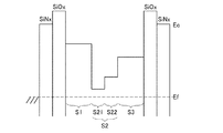
S2 第2の酸化物半導体層
S21 第1の領域
S22 第2の領域
S3 第3の酸化物半導体層
10a スパッタ装置
10b スパッタ装置
10c スパッタ装置
11 基板供給室
12a ロードロック室
12b ロードロック室
13 搬送室
14 カセットポート
15 基板加熱室
310 トランジスタ
320 トランジスタ
330 トランジスタ
400 基板
402 ゲート電極層
404 ゲート絶縁層
404a ゲート絶縁層
404b ゲート絶縁層
407a 酸化物半導体膜
407b 酸化物半導体膜
407b1 第1の領域
407b2 第2の領域
407c 酸化物半導体膜
408 酸化物半導体積層
408a 第1の酸化物半導体層
408b 第2の酸化物半導体層
408b1 第1の領域
408b2 第2の領域
408c 第3の酸化物半導体層
410 導電層
410a ソース電極層
410b ドレイン電極層
411 導電膜
412 絶縁層
412a 絶縁層
412b 絶縁層
428c 第3の酸化物半導体層
437a 酸化物半導体膜
437b 酸化物半導体膜
437c 酸化物半導体膜
438 酸化物半導体積層
438a 第1の酸化物半導体層
438b 第2の酸化物半導体層
438b1 第1の領域
438b2 第2の領域
438c 第3の酸化物半導体層
460 レジストマスク
462a レジストマスク
462b レジストマスク
500 基板
501 ゲート絶縁層
502 ゲート絶縁層
504 層間絶縁層
505 カラーフィルタ層
506 絶縁層
507 隔壁
510 トランジスタ
511a ゲート電極層
511b ゲート電極層
512 酸化物半導体積層
512a 第1の酸化物半導体層
512b 第2の酸化物半導体層
512c 第3の酸化物半導体層
513a 導電層
513b 導電層
520 容量素子
521a 導電層
521b 導電層
522 酸化物半導体積層
522a 第1の酸化物半導体層
522b 第2の酸化物半導体層
522c 第3の酸化物半導体層
523 導電層
525 絶縁層
530 配線層交差部
533 導電層
540 発光素子
541 電極層
542 電界発光層
543 電極層
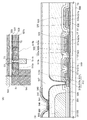
601 基板
602 フォトダイオード
606a 半導体膜
606b 半導体膜
606c 半導体膜
608 接着層
613 基板
632 絶縁層
633 層間絶縁層
634 層間絶縁層
640 トランジスタ
641a 電極層
641b 電極層
642 電極層
643 導電層
645 導電層
656 トランジスタ
658 フォトダイオードリセット信号線
659 ゲート信号線
671 フォトセンサ出力信号線
672 フォトセンサ基準信号線
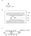
2000 基板
2001 スパッタリング粒子
2002 スパッタリングターゲット
2003 チャンバー
4001 基板
4002 画素部
4003 信号線駆動回路
4004 走査線駆動回路
4005 シール材
4006 基板
4008 液晶層
4010 トランジスタ
4011 トランジスタ
4013 液晶素子
4015 接続端子電極
4016 端子電極
4018 FPC
4019 異方性導電層
4020a ゲート絶縁層
4020b ゲート絶縁層
4031 電極層
4032a 絶縁層
4032b 絶縁層
4033 絶縁層
4034 電極層
4035 スペーサ
4038 絶縁層
4040 平坦化絶縁層
4042 絶縁層
9000 テーブル
9001 筐体
9002 脚部
9003 表示部
9004 表示ボタン
9005 電源コード
9033 留め具
9034 スイッチ
9035 電源スイッチ
9036 スイッチ
9038 操作スイッチ
9100 テレビジョン装置
9101 筐体
9103 表示部
9105 スタンド
9107 表示部
9109 操作キー
9110 リモコン操作機
9201 本体
9202 筐体
9203 表示部
9204 キーボード
9205 外部接続ポート
9206 ポインティングデバイス
9630 筐体
9631 表示部
9631a 表示部
9631b 表示部
9632a 領域
9632b 領域
9633 太陽電池
9634 充放電制御回路
9635 バッテリー
9636 DCDCコンバータ
9637 コンバータ
9638 操作キー
9639 ボタン
Claims (5)
- ゲート電極層と、
前記ゲート電極層上のゲート絶縁層と、
前記ゲート絶縁層を介して前記ゲート電極層と重畳し、第1の酸化物半導体層、第2の酸化物半導体層及び第3の酸化物半導体層の積層構造を含む酸化物半導体積層と、
前記酸化物半導体積層と電気的に接続するソース電極層及びドレイン電極層と、を有し、
前記第2の酸化物半導体層は、n型不純物を含有し、且つ、前記第2の酸化物半導体層において前記第1の酸化物半導体層と接する領域は、前記第2の酸化物半導体層において前記第3の酸化物半導体層と接する領域よりも高濃度で前記n型不純物を含有する半導体装置。 - ゲート電極層と、
前記ゲート電極層上のゲート絶縁層と、
前記ゲート絶縁層を介して前記ゲート電極層と重畳し、第1の酸化物半導体層、第2の酸化物半導体層及び第3の酸化物半導体層の積層構造を含む酸化物半導体積層と、
前記酸化物半導体積層と電気的に接続するソース電極層及びドレイン電極層と、を有し、
前記第2の酸化物半導体層は、n型不純物を含有し、且つ、前記第2の酸化物半導体層において前記第1の酸化物半導体層と接する領域は、前記第2の酸化物半導体層において前記第3の酸化物半導体層と接する領域よりも高濃度で前記n型不純物を含有し、
前記第1の酸化物半導体層乃至前記第3の酸化物半導体層を構成する金属元素のうち、少なくとも一は同一の金属元素である半導体装置。 - 請求項1又は2において、
前記第1の酸化物半導体層の膜厚は、前記第2の酸化物半導体層の膜厚よりも小さく、前記第3の酸化物半導体層の膜厚は、前記第2の酸化物半導体層の膜厚以上である半導体装置。 - 請求項1乃至3のいずれか一において、
前記第1の酸化物半導体層及び前記第3の酸化物半導体層は、i型の酸化物半導体層である半導体装置。 - 請求項1乃至4のいずれか一において、
前記第3の酸化物半導体層は、前記第1の酸化物半導体層及び前記第2の酸化物半導体層を覆うように設けられる半導体装置。
Priority Applications (1)
| Application Number | Priority Date | Filing Date | Title |
|---|---|---|---|
| JP2013134961A JP6130747B2 (ja) | 2012-06-29 | 2013-06-27 | 半導体装置 |
Applications Claiming Priority (3)
| Application Number | Priority Date | Filing Date | Title |
|---|---|---|---|
| JP2012147178 | 2012-06-29 | ||
| JP2012147178 | 2012-06-29 | ||
| JP2013134961A JP6130747B2 (ja) | 2012-06-29 | 2013-06-27 | 半導体装置 |
Related Child Applications (1)
| Application Number | Title | Priority Date | Filing Date |
|---|---|---|---|
| JP2017080483A Division JP6426228B2 (ja) | 2012-06-29 | 2017-04-14 | 半導体装置 |
Publications (2)
| Publication Number | Publication Date |
|---|---|
| JP2014030001A JP2014030001A (ja) | 2014-02-13 |
| JP6130747B2 true JP6130747B2 (ja) | 2017-05-17 |
Family
ID=49777165
Family Applications (4)
| Application Number | Title | Priority Date | Filing Date |
|---|---|---|---|
| JP2013134961A Active JP6130747B2 (ja) | 2012-06-29 | 2013-06-27 | 半導体装置 |
| JP2017080483A Expired - Fee Related JP6426228B2 (ja) | 2012-06-29 | 2017-04-14 | 半導体装置 |
| JP2018161344A Active JP6567150B2 (ja) | 2012-06-29 | 2018-08-30 | 半導体装置 |
| JP2019139682A Withdrawn JP2019195102A (ja) | 2012-06-29 | 2019-07-30 | 半導体装置 |
Family Applications After (3)
| Application Number | Title | Priority Date | Filing Date |
|---|---|---|---|
| JP2017080483A Expired - Fee Related JP6426228B2 (ja) | 2012-06-29 | 2017-04-14 | 半導体装置 |
| JP2018161344A Active JP6567150B2 (ja) | 2012-06-29 | 2018-08-30 | 半導体装置 |
| JP2019139682A Withdrawn JP2019195102A (ja) | 2012-06-29 | 2019-07-30 | 半導体装置 |
Country Status (3)
| Country | Link |
|---|---|
| US (3) | US8952381B2 (ja) |
| JP (4) | JP6130747B2 (ja) |
| KR (2) | KR102161077B1 (ja) |
Families Citing this family (67)
| Publication number | Priority date | Publication date | Assignee | Title |
|---|---|---|---|---|
| DE202011109498U1 (de) | 2011-12-27 | 2012-02-13 | Franz Haimer Maschinenbau Kg | Werkzeughalter und Spannsystem mit einem derartigen Werkzeughalter |
| TWI633371B (zh) | 2008-12-03 | 2018-08-21 | 半導體能源研究所股份有限公司 | 液晶顯示裝置 |
| CN105206514B (zh) | 2009-11-28 | 2018-04-10 | 株式会社半导体能源研究所 | 层叠的氧化物材料、半导体器件、以及用于制造该半导体器件的方法 |
| US8901557B2 (en) | 2012-06-15 | 2014-12-02 | Semiconductor Energy Laboratory Co., Ltd. | Semiconductor device |
| JP2014027263A (ja) * | 2012-06-15 | 2014-02-06 | Semiconductor Energy Lab Co Ltd | 半導体装置およびその作製方法 |
| US9059219B2 (en) | 2012-06-27 | 2015-06-16 | Semiconductor Energy Laboratory Co., Ltd. | Semiconductor device and method for manufacturing semiconductor device |
| US9190525B2 (en) | 2012-07-06 | 2015-11-17 | Semiconductor Energy Laboratory Co., Ltd. | Semiconductor device including oxide semiconductor layer |
| JP6134598B2 (ja) | 2012-08-02 | 2017-05-24 | 株式会社半導体エネルギー研究所 | 半導体装置 |
| SG11201505225TA (en) | 2012-08-03 | 2015-08-28 | Semiconductor Energy Lab | Oxide semiconductor stacked film and semiconductor device |
| JP6220597B2 (ja) | 2012-08-10 | 2017-10-25 | 株式会社半導体エネルギー研究所 | 半導体装置 |
| US9245958B2 (en) | 2012-08-10 | 2016-01-26 | Semiconductor Energy Laboratory Co., Ltd. | Semiconductor device and method for manufacturing the same |
| CN104584229B (zh) | 2012-08-10 | 2018-05-15 | 株式会社半导体能源研究所 | 半导体装置及其制造方法 |
| US9929276B2 (en) | 2012-08-10 | 2018-03-27 | Semiconductor Energy Laboratory Co., Ltd. | Semiconductor device and method for manufacturing the same |
| JP6211843B2 (ja) | 2012-08-10 | 2017-10-11 | 株式会社半導体エネルギー研究所 | 半導体装置 |
| TWI799011B (zh) | 2012-09-14 | 2023-04-11 | 日商半導體能源研究所股份有限公司 | 半導體裝置及其製造方法 |
| WO2014046222A1 (en) | 2012-09-24 | 2014-03-27 | Semiconductor Energy Laboratory Co., Ltd. | Display device |
| TWI746200B (zh) | 2012-09-24 | 2021-11-11 | 日商半導體能源研究所股份有限公司 | 半導體裝置 |
| JP5709810B2 (ja) * | 2012-10-02 | 2015-04-30 | キヤノン株式会社 | 検出装置の製造方法、その検出装置及び検出システム |
| WO2014061535A1 (en) | 2012-10-17 | 2014-04-24 | Semiconductor Energy Laboratory Co., Ltd. | Semiconductor device |
| WO2014061762A1 (en) | 2012-10-17 | 2014-04-24 | Semiconductor Energy Laboratory Co., Ltd. | Semiconductor device and method for manufacturing the same |
| KR102220279B1 (ko) | 2012-10-19 | 2021-02-24 | 가부시키가이샤 한도오따이 에네루기 켄큐쇼 | 산화물 반도체막을 포함하는 다층막 및 반도체 장치의 제작 방법 |
| JP6285150B2 (ja) | 2012-11-16 | 2018-02-28 | 株式会社半導体エネルギー研究所 | 半導体装置 |
| JP2014135478A (ja) | 2012-12-03 | 2014-07-24 | Semiconductor Energy Lab Co Ltd | 半導体装置およびその作製方法 |
| WO2014103901A1 (en) | 2012-12-25 | 2014-07-03 | Semiconductor Energy Laboratory Co., Ltd. | Semiconductor device and method for manufacturing the same |
| US9231111B2 (en) * | 2013-02-13 | 2016-01-05 | Semiconductor Energy Laboratory Co., Ltd. | Semiconductor device |
| US9190527B2 (en) | 2013-02-13 | 2015-11-17 | Semiconductor Energy Laboratory Co., Ltd. | Semiconductor device and manufacturing method of semiconductor device |
| KR102238682B1 (ko) | 2013-02-28 | 2021-04-08 | 가부시키가이샤 한도오따이 에네루기 켄큐쇼 | 반도체 장치와 그 제작 방법 |
| US9893192B2 (en) | 2013-04-24 | 2018-02-13 | Semiconductor Energy Laboratory Co., Ltd. | Semiconductor device |
| CN109888022A (zh) | 2013-05-20 | 2019-06-14 | 株式会社半导体能源研究所 | 半导体装置 |
| KR102061306B1 (ko) * | 2013-06-14 | 2019-12-31 | 한국전자통신연구원 | 트랜지스터 및 그 제조방법 |
| US20150008428A1 (en) | 2013-07-08 | 2015-01-08 | Semiconductor Energy Laboratory Co., Ltd. | Semiconductor device and method for manufacturing semiconductor device |
| KR101457812B1 (ko) * | 2013-08-19 | 2014-11-05 | 포항공과대학교 산학협력단 | 양방향 스위칭 특성을 갖는 2-단자 스위칭 소자, 이의 제조방법 및 이를 포함하는 저항성 메모리 소자 크로스-포인트 어레이 |
| TWI646690B (zh) | 2013-09-13 | 2019-01-01 | 半導體能源研究所股份有限公司 | 半導體裝置及其製造方法 |
| WO2015083034A1 (en) * | 2013-12-02 | 2015-06-11 | Semiconductor Energy Laboratory Co., Ltd. | Display device |
| US9349751B2 (en) | 2013-12-12 | 2016-05-24 | Semiconductor Energy Laboratory Co., Ltd. | Semiconductor device |
| TWI721409B (zh) | 2013-12-19 | 2021-03-11 | 日商半導體能源研究所股份有限公司 | 半導體裝置 |
| WO2015097596A1 (en) * | 2013-12-26 | 2015-07-02 | Semiconductor Energy Laboratory Co., Ltd. | Semiconductor device |
| JP2015188062A (ja) | 2014-02-07 | 2015-10-29 | 株式会社半導体エネルギー研究所 | 半導体装置 |
| WO2015125042A1 (en) | 2014-02-19 | 2015-08-27 | Semiconductor Energy Laboratory Co., Ltd. | Oxide, semiconductor device, module, and electronic device |
| TWI675004B (zh) | 2014-02-21 | 2019-10-21 | 日商半導體能源研究所股份有限公司 | 半導體膜、電晶體、半導體裝置、顯示裝置以及電子裝置 |
| TWI663726B (zh) | 2014-05-30 | 2019-06-21 | Semiconductor Energy Laboratory Co., Ltd. | 半導體裝置、模組及電子裝置 |
| US10269832B2 (en) * | 2014-10-10 | 2019-04-23 | Joled Inc. | Thin film transistor substrate, method for manufacturing thin film transistor substrate, and display panel |
| US10164118B2 (en) * | 2014-11-28 | 2018-12-25 | Sharp Kabushiki Kaisha | Semiconductor device and method for producing same |
| US20160155803A1 (en) * | 2014-11-28 | 2016-06-02 | Semiconductor Energy Laboratory Co., Ltd. | Semiconductor Device, Method for Manufacturing the Semiconductor Device, and Display Device Including the Semiconductor Device |
| CN114512547A (zh) | 2015-02-12 | 2022-05-17 | 株式会社半导体能源研究所 | 氧化物半导体膜及半导体装置 |
| US9842938B2 (en) | 2015-03-24 | 2017-12-12 | Semiconductor Energy Laboratory Co., Ltd. | Semiconductor device and display device including semiconductor device |
| KR20160114511A (ko) | 2015-03-24 | 2016-10-05 | 가부시키가이샤 한도오따이 에네루기 켄큐쇼 | 반도체 장치의 제작 방법 |
| US9806200B2 (en) | 2015-03-27 | 2017-10-31 | Semiconductor Energy Laboratory Co., Ltd. | Semiconductor device |
| CN104916703B (zh) * | 2015-05-07 | 2018-07-31 | 京东方科技集团股份有限公司 | 一种氧化物薄膜晶体管、阵列基板和显示装置 |
| TWI650817B (zh) * | 2015-08-28 | 2019-02-11 | 聯華電子股份有限公司 | 半導體元件及其製作方法 |
| US10714633B2 (en) | 2015-12-15 | 2020-07-14 | Semiconductor Energy Laboratory Co., Ltd. | Semiconductor device and display device |
| KR20230043237A (ko) | 2016-03-11 | 2023-03-30 | 가부시키가이샤 한도오따이 에네루기 켄큐쇼 | 복합체 및 트랜지스터 |
| WO2017153882A1 (en) | 2016-03-11 | 2017-09-14 | Semiconductor Energy Laboratory Co., Ltd. | Semiconductor device, manufacturing method thereof, and display device including the semiconductor device |
| US11302717B2 (en) * | 2016-04-08 | 2022-04-12 | Semiconductor Energy Laboratory Co., Ltd. | Transistor and method for manufacturing the same |
| TWI737665B (zh) | 2016-07-01 | 2021-09-01 | 日商半導體能源硏究所股份有限公司 | 半導體裝置以及半導體裝置的製造方法 |
| TWI754542B (zh) | 2016-07-11 | 2022-02-01 | 日商半導體能源研究所股份有限公司 | 濺射靶材及金屬氧化物 |
| TW202343784A (zh) | 2016-07-11 | 2023-11-01 | 日商半導體能源研究所股份有限公司 | 金屬氧化物及半導體裝置 |
| DE112017004841T5 (de) * | 2016-09-27 | 2019-06-19 | Sharp Kabushiki Kaisha | Halbleitervorrichtung und Verfahren zu deren Herstellung |
| US9837497B1 (en) * | 2016-10-18 | 2017-12-05 | United Microelectronics Corp. | Channel structure and manufacturing method thereof |
| US10866475B2 (en) | 2017-03-17 | 2020-12-15 | Sharp Kabushiki Kaisha | Active matrix substrate and display device |
| CN107316897B (zh) * | 2017-06-28 | 2020-02-14 | 上海天马有机发光显示技术有限公司 | 显示基板、显示装置及显示基板的制作方法 |
| US11387330B2 (en) | 2018-03-12 | 2022-07-12 | Semiconductor Energy Laboratory Co., Ltd. | Metal oxide and transistor including metal oxide |
| KR20200076343A (ko) * | 2018-12-19 | 2020-06-29 | 엘지디스플레이 주식회사 | 박막 트랜지스터 및 이를 포함하는 표시장치 |
| WO2020245925A1 (ja) * | 2019-06-04 | 2020-12-10 | 堺ディスプレイプロダクト株式会社 | 薄膜トランジスタおよびその製造方法、ならびに表示装置 |
| US20210376156A1 (en) * | 2020-05-29 | 2021-12-02 | Taiwan Semiconductor Manufacturing Company Limited | Raised source/drain oxide semiconducting thin film transistor and methods of making the same |
| US11721767B2 (en) | 2020-06-29 | 2023-08-08 | Taiwan Semiconductor Manufacturing Company Limited | Oxide semiconductor transistor structure in 3-D device and methods of forming the same |
| KR102486098B1 (ko) * | 2022-04-08 | 2023-01-09 | 주식회사 나노신소재 | 산화물 소결체 및 이를 포함하는 박막 트랜지스터 |
Family Cites Families (156)
| Publication number | Priority date | Publication date | Assignee | Title |
|---|---|---|---|---|
| JPS60160170A (ja) * | 1984-01-31 | 1985-08-21 | Seiko Instr & Electronics Ltd | 薄膜トランジスタ |
| JPS60198861A (ja) | 1984-03-23 | 1985-10-08 | Fujitsu Ltd | 薄膜トランジスタ |
| JPH0244256B2 (ja) | 1987-01-28 | 1990-10-03 | Kagaku Gijutsucho Mukizaishitsu Kenkyushocho | Ingazn2o5deshimesarerurotsuhoshokeinosojokozoojusurukagobutsuoyobisonoseizoho |
| JPH0244258B2 (ja) | 1987-02-24 | 1990-10-03 | Kagaku Gijutsucho Mukizaishitsu Kenkyushocho | Ingazn3o6deshimesarerurotsuhoshokeinosojokozoojusurukagobutsuoyobisonoseizoho |
| JPS63210023A (ja) | 1987-02-24 | 1988-08-31 | Natl Inst For Res In Inorg Mater | InGaZn↓4O↓7で示される六方晶系の層状構造を有する化合物およびその製造法 |
| JPH0244260B2 (ja) | 1987-02-24 | 1990-10-03 | Kagaku Gijutsucho Mukizaishitsu Kenkyushocho | Ingazn5o8deshimesarerurotsuhoshokeinosojokozoojusurukagobutsuoyobisonoseizoho |
| JPH0244262B2 (ja) | 1987-02-27 | 1990-10-03 | Kagaku Gijutsucho Mukizaishitsu Kenkyushocho | Ingazn6o9deshimesarerurotsuhoshokeinosojokozoojusurukagobutsuoyobisonoseizoho |
| JPS63258072A (ja) * | 1987-04-15 | 1988-10-25 | Nec Corp | 電界効果トランジスタ |
| JPH0244263B2 (ja) | 1987-04-22 | 1990-10-03 | Kagaku Gijutsucho Mukizaishitsu Kenkyushocho | Ingazn7o10deshimesarerurotsuhoshokeinosojokozoojusurukagobutsuoyobisonoseizoho |
| JPH05251705A (ja) | 1992-03-04 | 1993-09-28 | Fuji Xerox Co Ltd | 薄膜トランジスタ |
| JP3479375B2 (ja) | 1995-03-27 | 2003-12-15 | 科学技術振興事業団 | 亜酸化銅等の金属酸化物半導体による薄膜トランジスタとpn接合を形成した金属酸化物半導体装置およびそれらの製造方法 |
| EP0820644B1 (en) | 1995-08-03 | 2005-08-24 | Koninklijke Philips Electronics N.V. | Semiconductor device provided with transparent switching element |
| JP3625598B2 (ja) | 1995-12-30 | 2005-03-02 | 三星電子株式会社 | 液晶表示装置の製造方法 |
| JP4170454B2 (ja) | 1998-07-24 | 2008-10-22 | Hoya株式会社 | 透明導電性酸化物薄膜を有する物品及びその製造方法 |
| JP2000150861A (ja) | 1998-11-16 | 2000-05-30 | Tdk Corp | 酸化物薄膜 |
| JP3276930B2 (ja) | 1998-11-17 | 2002-04-22 | 科学技術振興事業団 | トランジスタ及び半導体装置 |
| TW460731B (en) | 1999-09-03 | 2001-10-21 | Ind Tech Res Inst | Electrode structure and production method of wide viewing angle LCD |
| JP4089858B2 (ja) | 2000-09-01 | 2008-05-28 | 国立大学法人東北大学 | 半導体デバイス |
| KR20020038482A (ko) | 2000-11-15 | 2002-05-23 | 모리시타 요이찌 | 박막 트랜지스터 어레이, 그 제조방법 및 그것을 이용한표시패널 |
| JP3997731B2 (ja) | 2001-03-19 | 2007-10-24 | 富士ゼロックス株式会社 | 基材上に結晶性半導体薄膜を形成する方法 |
| JP2002289859A (ja) | 2001-03-23 | 2002-10-04 | Minolta Co Ltd | 薄膜トランジスタ |
| KR100941241B1 (ko) | 2001-08-02 | 2010-02-10 | 이데미쓰 고산 가부시키가이샤 | 스퍼터링 타겟, 투명 전도막 및 이들의 제조방법 |
| JP4090716B2 (ja) | 2001-09-10 | 2008-05-28 | 雅司 川崎 | 薄膜トランジスタおよびマトリクス表示装置 |
| JP3925839B2 (ja) | 2001-09-10 | 2007-06-06 | シャープ株式会社 | 半導体記憶装置およびその試験方法 |
| JP4164562B2 (ja) | 2002-09-11 | 2008-10-15 | 独立行政法人科学技術振興機構 | ホモロガス薄膜を活性層として用いる透明薄膜電界効果型トランジスタ |
| EP1443130B1 (en) | 2001-11-05 | 2011-09-28 | Japan Science and Technology Agency | Natural superlattice homologous single crystal thin film, method for preparation thereof, and device using said single crystal thin film |
| JP4083486B2 (ja) | 2002-02-21 | 2008-04-30 | 独立行政法人科学技術振興機構 | LnCuO(S,Se,Te)単結晶薄膜の製造方法 |
| US7049190B2 (en) | 2002-03-15 | 2006-05-23 | Sanyo Electric Co., Ltd. | Method for forming ZnO film, method for forming ZnO semiconductor layer, method for fabricating semiconductor device, and semiconductor device |
| JP3933591B2 (ja) | 2002-03-26 | 2007-06-20 | 淳二 城戸 | 有機エレクトロルミネッセント素子 |
| US7339187B2 (en) | 2002-05-21 | 2008-03-04 | State Of Oregon Acting By And Through The Oregon State Board Of Higher Education On Behalf Of Oregon State University | Transistor structures |
| JP2004022625A (ja) | 2002-06-13 | 2004-01-22 | Murata Mfg Co Ltd | 半導体デバイス及び該半導体デバイスの製造方法 |
| US7105868B2 (en) | 2002-06-24 | 2006-09-12 | Cermet, Inc. | High-electron mobility transistor with zinc oxide |
| US7067843B2 (en) | 2002-10-11 | 2006-06-27 | E. I. Du Pont De Nemours And Company | Transparent oxide semiconductor thin film transistors |
| JP4166105B2 (ja) | 2003-03-06 | 2008-10-15 | シャープ株式会社 | 半導体装置およびその製造方法 |
| JP2004273732A (ja) | 2003-03-07 | 2004-09-30 | Sharp Corp | アクティブマトリクス基板およびその製造方法 |
| CA2521678A1 (en) * | 2003-04-11 | 2004-10-28 | Vertex Pharmaceuticals, Incorporated | Inhibitors of serine proteases, particularly hcv ns3-ns4a protease |
| JP4108633B2 (ja) | 2003-06-20 | 2008-06-25 | シャープ株式会社 | 薄膜トランジスタおよびその製造方法ならびに電子デバイス |
| US7262463B2 (en) | 2003-07-25 | 2007-08-28 | Hewlett-Packard Development Company, L.P. | Transistor including a deposited channel region having a doped portion |
| US20050017244A1 (en) | 2003-07-25 | 2005-01-27 | Randy Hoffman | Semiconductor device |
| EP2246894B2 (en) | 2004-03-12 | 2018-10-10 | Japan Science and Technology Agency | Method for fabricating a thin film transistor having an amorphous oxide as a channel layer |
| US7282782B2 (en) | 2004-03-12 | 2007-10-16 | Hewlett-Packard Development Company, L.P. | Combined binary oxide semiconductor device |
| US7297977B2 (en) | 2004-03-12 | 2007-11-20 | Hewlett-Packard Development Company, L.P. | Semiconductor device |
| US7145174B2 (en) | 2004-03-12 | 2006-12-05 | Hewlett-Packard Development Company, Lp. | Semiconductor device |
| US7211825B2 (en) | 2004-06-14 | 2007-05-01 | Yi-Chi Shih | Indium oxide-based thin film transistors and circuits |
| JP2006100760A (ja) | 2004-09-02 | 2006-04-13 | Casio Comput Co Ltd | 薄膜トランジスタおよびその製造方法 |
| US7285501B2 (en) | 2004-09-17 | 2007-10-23 | Hewlett-Packard Development Company, L.P. | Method of forming a solution processed device |
| US7298084B2 (en) | 2004-11-02 | 2007-11-20 | 3M Innovative Properties Company | Methods and displays utilizing integrated zinc oxide row and column drivers in conjunction with organic light emitting diodes |
| US7829444B2 (en) | 2004-11-10 | 2010-11-09 | Canon Kabushiki Kaisha | Field effect transistor manufacturing method |
| US7868326B2 (en) | 2004-11-10 | 2011-01-11 | Canon Kabushiki Kaisha | Field effect transistor |
| KR20070085879A (ko) | 2004-11-10 | 2007-08-27 | 캐논 가부시끼가이샤 | 발광 장치 |
| US7863611B2 (en) | 2004-11-10 | 2011-01-04 | Canon Kabushiki Kaisha | Integrated circuits utilizing amorphous oxides |
| US7791072B2 (en) | 2004-11-10 | 2010-09-07 | Canon Kabushiki Kaisha | Display |
| RU2402106C2 (ru) | 2004-11-10 | 2010-10-20 | Кэнон Кабусики Кайся | Аморфный оксид и полевой транзистор с его использованием |
| US7453065B2 (en) | 2004-11-10 | 2008-11-18 | Canon Kabushiki Kaisha | Sensor and image pickup device |
| US7579224B2 (en) | 2005-01-21 | 2009-08-25 | Semiconductor Energy Laboratory Co., Ltd. | Method for manufacturing a thin film semiconductor device |
| TWI445178B (zh) | 2005-01-28 | 2014-07-11 | Semiconductor Energy Lab | 半導體裝置,電子裝置,和半導體裝置的製造方法 |
| TWI412138B (zh) | 2005-01-28 | 2013-10-11 | Semiconductor Energy Lab | 半導體裝置,電子裝置,和半導體裝置的製造方法 |
| US7858451B2 (en) | 2005-02-03 | 2010-12-28 | Semiconductor Energy Laboratory Co., Ltd. | Electronic device, semiconductor device and manufacturing method thereof |
| US7948171B2 (en) | 2005-02-18 | 2011-05-24 | Semiconductor Energy Laboratory Co., Ltd. | Light emitting device |
| US20060197092A1 (en) | 2005-03-03 | 2006-09-07 | Randy Hoffman | System and method for forming conductive material on a substrate |
| US8681077B2 (en) | 2005-03-18 | 2014-03-25 | Semiconductor Energy Laboratory Co., Ltd. | Semiconductor device, and display device, driving method and electronic apparatus thereof |
| WO2006105077A2 (en) | 2005-03-28 | 2006-10-05 | Massachusetts Institute Of Technology | Low voltage thin film transistor with high-k dielectric material |
| US7645478B2 (en) | 2005-03-31 | 2010-01-12 | 3M Innovative Properties Company | Methods of making displays |
| US8300031B2 (en) | 2005-04-20 | 2012-10-30 | Semiconductor Energy Laboratory Co., Ltd. | Semiconductor device comprising transistor having gate and drain connected through a current-voltage conversion element |
| JP2006344849A (ja) | 2005-06-10 | 2006-12-21 | Casio Comput Co Ltd | 薄膜トランジスタ |
| US7402506B2 (en) | 2005-06-16 | 2008-07-22 | Eastman Kodak Company | Methods of making thin film transistors comprising zinc-oxide-based semiconductor materials and transistors made thereby |
| US7691666B2 (en) | 2005-06-16 | 2010-04-06 | Eastman Kodak Company | Methods of making thin film transistors comprising zinc-oxide-based semiconductor materials and transistors made thereby |
| US7507618B2 (en) | 2005-06-27 | 2009-03-24 | 3M Innovative Properties Company | Method for making electronic devices using metal oxide nanoparticles |
| KR100711890B1 (ko) | 2005-07-28 | 2007-04-25 | 삼성에스디아이 주식회사 | 유기 발광표시장치 및 그의 제조방법 |
| JP2007059128A (ja) | 2005-08-23 | 2007-03-08 | Canon Inc | 有機el表示装置およびその製造方法 |
| JP4850457B2 (ja) | 2005-09-06 | 2012-01-11 | キヤノン株式会社 | 薄膜トランジスタ及び薄膜ダイオード |
| JP2007073705A (ja) | 2005-09-06 | 2007-03-22 | Canon Inc | 酸化物半導体チャネル薄膜トランジスタおよびその製造方法 |
| JP5116225B2 (ja) | 2005-09-06 | 2013-01-09 | キヤノン株式会社 | 酸化物半導体デバイスの製造方法 |
| JP4280736B2 (ja) | 2005-09-06 | 2009-06-17 | キヤノン株式会社 | 半導体素子 |
| JP5064747B2 (ja) | 2005-09-29 | 2012-10-31 | 株式会社半導体エネルギー研究所 | 半導体装置、電気泳動表示装置、表示モジュール、電子機器、及び半導体装置の作製方法 |
| JP5078246B2 (ja) | 2005-09-29 | 2012-11-21 | 株式会社半導体エネルギー研究所 | 半導体装置、及び半導体装置の作製方法 |
| EP1998375A3 (en) | 2005-09-29 | 2012-01-18 | Semiconductor Energy Laboratory Co, Ltd. | Semiconductor device having oxide semiconductor layer and manufacturing method |
| JP5037808B2 (ja) | 2005-10-20 | 2012-10-03 | キヤノン株式会社 | アモルファス酸化物を用いた電界効果型トランジスタ、及び該トランジスタを用いた表示装置 |
| KR20090115222A (ko) | 2005-11-15 | 2009-11-04 | 가부시키가이샤 한도오따이 에네루기 켄큐쇼 | 반도체장치 제조방법 |
| TWI292281B (en) | 2005-12-29 | 2008-01-01 | Ind Tech Res Inst | Pixel structure of active organic light emitting diode and method of fabricating the same |
| US7867636B2 (en) | 2006-01-11 | 2011-01-11 | Murata Manufacturing Co., Ltd. | Transparent conductive film and method for manufacturing the same |
| JP4977478B2 (ja) | 2006-01-21 | 2012-07-18 | 三星電子株式会社 | ZnOフィルム及びこれを用いたTFTの製造方法 |
| US7576394B2 (en) | 2006-02-02 | 2009-08-18 | Kochi Industrial Promotion Center | Thin film transistor including low resistance conductive thin films and manufacturing method thereof |
| US7977169B2 (en) | 2006-02-15 | 2011-07-12 | Kochi Industrial Promotion Center | Semiconductor device including active layer made of zinc oxide with controlled orientations and manufacturing method thereof |
| KR20070101595A (ko) | 2006-04-11 | 2007-10-17 | 삼성전자주식회사 | ZnO TFT |
| US20070252928A1 (en) | 2006-04-28 | 2007-11-01 | Toppan Printing Co., Ltd. | Structure, transmission type liquid crystal display, reflection type display and manufacturing method thereof |
| JP5028033B2 (ja) | 2006-06-13 | 2012-09-19 | キヤノン株式会社 | 酸化物半導体膜のドライエッチング方法 |
| JP4999400B2 (ja) | 2006-08-09 | 2012-08-15 | キヤノン株式会社 | 酸化物半導体膜のドライエッチング方法 |
| JP4609797B2 (ja) | 2006-08-09 | 2011-01-12 | Nec液晶テクノロジー株式会社 | 薄膜デバイス及びその製造方法 |
| JP4332545B2 (ja) | 2006-09-15 | 2009-09-16 | キヤノン株式会社 | 電界効果型トランジスタ及びその製造方法 |
| JP4274219B2 (ja) | 2006-09-27 | 2009-06-03 | セイコーエプソン株式会社 | 電子デバイス、有機エレクトロルミネッセンス装置、有機薄膜半導体装置 |
| JP5164357B2 (ja) | 2006-09-27 | 2013-03-21 | キヤノン株式会社 | 半導体装置及び半導体装置の製造方法 |
| US7622371B2 (en) | 2006-10-10 | 2009-11-24 | Hewlett-Packard Development Company, L.P. | Fused nanocrystal thin film semiconductor and method |
| US7772021B2 (en) | 2006-11-29 | 2010-08-10 | Samsung Electronics Co., Ltd. | Flat panel displays comprising a thin-film transistor having a semiconductive oxide in its channel and methods of fabricating the same for use in flat panel displays |
| JP2008140684A (ja) | 2006-12-04 | 2008-06-19 | Toppan Printing Co Ltd | カラーelディスプレイおよびその製造方法 |
| KR101303578B1 (ko) | 2007-01-05 | 2013-09-09 | 삼성전자주식회사 | 박막 식각 방법 |
| US8207063B2 (en) | 2007-01-26 | 2012-06-26 | Eastman Kodak Company | Process for atomic layer deposition |
| KR100851215B1 (ko) | 2007-03-14 | 2008-08-07 | 삼성에스디아이 주식회사 | 박막 트랜지스터 및 이를 이용한 유기 전계 발광표시장치 |
| US7795613B2 (en) | 2007-04-17 | 2010-09-14 | Toppan Printing Co., Ltd. | Structure with transistor |
| KR101325053B1 (ko) | 2007-04-18 | 2013-11-05 | 삼성디스플레이 주식회사 | 박막 트랜지스터 기판 및 이의 제조 방법 |
| KR20080094300A (ko) | 2007-04-19 | 2008-10-23 | 삼성전자주식회사 | 박막 트랜지스터 및 그 제조 방법과 박막 트랜지스터를포함하는 평판 디스플레이 |
| KR101334181B1 (ko) | 2007-04-20 | 2013-11-28 | 삼성전자주식회사 | 선택적으로 결정화된 채널층을 갖는 박막 트랜지스터 및 그제조 방법 |
| CN101663762B (zh) | 2007-04-25 | 2011-09-21 | 佳能株式会社 | 氧氮化物半导体 |
| KR101345376B1 (ko) | 2007-05-29 | 2013-12-24 | 삼성전자주식회사 | ZnO 계 박막 트랜지스터 및 그 제조방법 |
| US8202365B2 (en) | 2007-12-17 | 2012-06-19 | Fujifilm Corporation | Process for producing oriented inorganic crystalline film, and semiconductor device using the oriented inorganic crystalline film |
| US8704217B2 (en) * | 2008-01-17 | 2014-04-22 | Idemitsu Kosan Co., Ltd. | Field effect transistor, semiconductor device and semiconductor device manufacturing method |
| JP4555358B2 (ja) | 2008-03-24 | 2010-09-29 | 富士フイルム株式会社 | 薄膜電界効果型トランジスタおよび表示装置 |
| KR100941850B1 (ko) | 2008-04-03 | 2010-02-11 | 삼성모바일디스플레이주식회사 | 박막 트랜지스터, 그의 제조 방법 및 박막 트랜지스터를구비하는 평판 표시 장치 |
| KR100963026B1 (ko) | 2008-06-30 | 2010-06-10 | 삼성모바일디스플레이주식회사 | 박막 트랜지스터, 그의 제조 방법 및 박막 트랜지스터를구비하는 평판 표시 장치 |
| KR100963027B1 (ko) | 2008-06-30 | 2010-06-10 | 삼성모바일디스플레이주식회사 | 박막 트랜지스터, 그의 제조 방법 및 박막 트랜지스터를구비하는 평판 표시 장치 |
| JP5345456B2 (ja) | 2008-08-14 | 2013-11-20 | 富士フイルム株式会社 | 薄膜電界効果型トランジスタ |
| JP5345359B2 (ja) | 2008-09-18 | 2013-11-20 | 富士フイルム株式会社 | 薄膜電界効果型トランジスタおよびそれを用いた表示装置 |
| JP4623179B2 (ja) | 2008-09-18 | 2011-02-02 | ソニー株式会社 | 薄膜トランジスタおよびその製造方法 |
| JP5451280B2 (ja) | 2008-10-09 | 2014-03-26 | キヤノン株式会社 | ウルツ鉱型結晶成長用基板およびその製造方法ならびに半導体装置 |
| KR101034686B1 (ko) * | 2009-01-12 | 2011-05-16 | 삼성모바일디스플레이주식회사 | 유기전계발광 표시 장치 및 그의 제조 방법 |
| US8492756B2 (en) | 2009-01-23 | 2013-07-23 | Semiconductor Energy Laboratory Co., Ltd. | Semiconductor device and method for manufacturing the same |
| JP5606682B2 (ja) | 2009-01-29 | 2014-10-15 | 富士フイルム株式会社 | 薄膜トランジスタ、多結晶酸化物半導体薄膜の製造方法、及び薄膜トランジスタの製造方法 |
| US8704216B2 (en) * | 2009-02-27 | 2014-04-22 | Semiconductor Energy Laboratory Co., Ltd. | Semiconductor device and manufacturing method thereof |
| JP5322787B2 (ja) * | 2009-06-11 | 2013-10-23 | 富士フイルム株式会社 | 薄膜トランジスタ及びその製造方法、電気光学装置、並びにセンサー |
| JP4571221B1 (ja) | 2009-06-22 | 2010-10-27 | 富士フイルム株式会社 | Igzo系酸化物材料及びigzo系酸化物材料の製造方法 |
| JP4415062B1 (ja) | 2009-06-22 | 2010-02-17 | 富士フイルム株式会社 | 薄膜トランジスタ及び薄膜トランジスタの製造方法 |
| US20110014010A1 (en) * | 2009-07-20 | 2011-01-20 | Aztec Washer Company | Washer with vulcanizate layer |
| JP5663231B2 (ja) | 2009-08-07 | 2015-02-04 | 株式会社半導体エネルギー研究所 | 発光装置 |
| WO2011039853A1 (ja) * | 2009-09-30 | 2011-04-07 | キヤノン株式会社 | 薄膜トランジスタ |
| CN103400857B (zh) | 2009-11-27 | 2016-12-28 | 株式会社半导体能源研究所 | 半导体装置和及其制造方法 |
| US20120280227A1 (en) | 2009-11-27 | 2012-11-08 | Hironori Wakana | Oxide semiconductor device and method of manufacturing the same |
| KR101520024B1 (ko) | 2009-11-28 | 2015-05-14 | 가부시키가이샤 한도오따이 에네루기 켄큐쇼 | 반도체 장치 및 그 제작 방법 |
| KR101943109B1 (ko) * | 2009-12-04 | 2019-01-28 | 가부시키가이샤 한도오따이 에네루기 켄큐쇼 | 반도체 장치 및 그 제조 방법 |
| JP5497417B2 (ja) * | 2009-12-10 | 2014-05-21 | 富士フイルム株式会社 | 薄膜トランジスタおよびその製造方法、並びにその薄膜トランジスタを備えた装置 |
| WO2011081009A1 (en) * | 2009-12-28 | 2011-07-07 | Semiconductor Energy Laboratory Co., Ltd. | Method for manufacturing semiconductor device |
| JP2011138934A (ja) | 2009-12-28 | 2011-07-14 | Sony Corp | 薄膜トランジスタ、表示装置および電子機器 |
| JP2011187506A (ja) | 2010-03-04 | 2011-09-22 | Sony Corp | 薄膜トランジスタおよびその製造方法、並びに表示装置 |
| KR102141064B1 (ko) | 2010-04-02 | 2020-08-04 | 가부시키가이샤 한도오따이 에네루기 켄큐쇼 | 반도체 장치 |
| JP5606787B2 (ja) | 2010-05-18 | 2014-10-15 | 富士フイルム株式会社 | 薄膜トランジスタの製造方法、並びに、薄膜トランジスタ、イメージセンサー、x線センサー及びx線デジタル撮影装置 |
| US9209314B2 (en) | 2010-06-16 | 2015-12-08 | Semiconductor Energy Laboratory Co., Ltd. | Field effect transistor |
| KR20110139394A (ko) | 2010-06-23 | 2011-12-29 | 주성엔지니어링(주) | 박막 트랜지스터 및 그 제조 방법 |
| JP5453663B2 (ja) | 2010-07-02 | 2014-03-26 | 合同会社先端配線材料研究所 | 薄膜トランジスタ |
| TWI615920B (zh) * | 2010-08-06 | 2018-02-21 | 半導體能源研究所股份有限公司 | 半導體裝置及其製造方法 |
| US8835917B2 (en) | 2010-09-13 | 2014-09-16 | Semiconductor Energy Laboratory Co., Ltd. | Semiconductor device, power diode, and rectifier |
| US8592879B2 (en) * | 2010-09-13 | 2013-11-26 | Semiconductor Energy Laboratory Co., Ltd. | Method for manufacturing semiconductor device |
| TWI555205B (zh) | 2010-11-05 | 2016-10-21 | 半導體能源研究所股份有限公司 | 半導體裝置及半導體裝置的製造方法 |
| US8629496B2 (en) * | 2010-11-30 | 2014-01-14 | Semiconductor Energy Laboratory Co., Ltd. | Semiconductor device and method for manufacturing the same |
| TWI562379B (en) * | 2010-11-30 | 2016-12-11 | Semiconductor Energy Lab Co Ltd | Semiconductor device and method for manufacturing semiconductor device |
| JP2012160679A (ja) | 2011-02-03 | 2012-08-23 | Sony Corp | 薄膜トランジスタ、表示装置および電子機器 |
| US8686416B2 (en) * | 2011-03-25 | 2014-04-01 | Semiconductor Energy Laboratory Co., Ltd. | Oxide semiconductor film and semiconductor device |
| KR102432070B1 (ko) | 2011-06-08 | 2022-08-11 | 가부시키가이샤 한도오따이 에네루기 켄큐쇼 | 스퍼터링 타겟, 스퍼터링 타겟의 제조 방법 및 박막의 형성 방법 |
| WO2013089115A1 (en) | 2011-12-15 | 2013-06-20 | Semiconductor Energy Laboratory Co., Ltd. | Semiconductor device and method for manufacturing the same |
| JP6059566B2 (ja) | 2012-04-13 | 2017-01-11 | 株式会社半導体エネルギー研究所 | 半導体装置の作製方法 |
| DE102013022449B3 (de) | 2012-05-11 | 2019-11-07 | Semiconductor Energy Laboratory Co., Ltd. | Halbleitervorrichtung und elektronisches Gerät |
| CN104380473B (zh) | 2012-05-31 | 2017-10-13 | 株式会社半导体能源研究所 | 半导体装置 |
| KR102119914B1 (ko) | 2012-05-31 | 2020-06-05 | 가부시키가이샤 한도오따이 에네루기 켄큐쇼 | 반도체 장치 및 그 제작 방법 |
| US9134864B2 (en) | 2012-05-31 | 2015-09-15 | Semiconductor Energy Laboratory Co., Ltd. | Electronic device with controller and touch panel for rapid restoration from power-saving mode |
| US20130320335A1 (en) | 2012-06-01 | 2013-12-05 | Semiconductor Energy Laboratory Co., Ltd. | Semiconductor device and method for manufacturing the same |
| JP2014027263A (ja) | 2012-06-15 | 2014-02-06 | Semiconductor Energy Lab Co Ltd | 半導体装置およびその作製方法 |
| US8901557B2 (en) | 2012-06-15 | 2014-12-02 | Semiconductor Energy Laboratory Co., Ltd. | Semiconductor device |
| US20130341180A1 (en) | 2012-06-22 | 2013-12-26 | Semiconductor Energy Laboratory Co., Ltd. | Sputtering target and method for using the same |
-
2013
- 2013-06-11 KR KR1020130066704A patent/KR102161077B1/ko active IP Right Grant
- 2013-06-18 US US13/920,417 patent/US8952381B2/en active Active
- 2013-06-27 JP JP2013134961A patent/JP6130747B2/ja active Active
-
2015
- 2015-01-13 US US14/595,664 patent/US9666721B2/en active Active
- 2015-01-15 KR KR1020150007582A patent/KR102095939B1/ko active IP Right Grant
-
2017
- 2017-04-14 JP JP2017080483A patent/JP6426228B2/ja not_active Expired - Fee Related
- 2017-05-25 US US15/605,132 patent/US10424673B2/en active Active
-
2018
- 2018-08-30 JP JP2018161344A patent/JP6567150B2/ja active Active
-
2019
- 2019-07-30 JP JP2019139682A patent/JP2019195102A/ja not_active Withdrawn
Also Published As
| Publication number | Publication date |
|---|---|
| US9666721B2 (en) | 2017-05-30 |
| US20140001465A1 (en) | 2014-01-02 |
| JP2014030001A (ja) | 2014-02-13 |
| KR20150022943A (ko) | 2015-03-04 |
| US10424673B2 (en) | 2019-09-24 |
| KR102161077B1 (ko) | 2020-09-29 |
| JP2017126795A (ja) | 2017-07-20 |
| KR20140002496A (ko) | 2014-01-08 |
| JP6426228B2 (ja) | 2018-11-21 |
| JP2018201041A (ja) | 2018-12-20 |
| US8952381B2 (en) | 2015-02-10 |
| KR102095939B1 (ko) | 2020-04-01 |
| JP6567150B2 (ja) | 2019-08-28 |
| US20170263775A1 (en) | 2017-09-14 |
| JP2019195102A (ja) | 2019-11-07 |
| US20150123127A1 (en) | 2015-05-07 |
Similar Documents
| Publication | Publication Date | Title |
|---|---|---|
| JP6567150B2 (ja) | 半導体装置 | |
| JP7362861B2 (ja) | 半導体装置 | |
| JP6227287B2 (ja) | 半導体装置 | |
| JP6212192B2 (ja) | 半導体装置 | |
| JP6409089B2 (ja) | 半導体装置 | |
| JP6134598B2 (ja) | 半導体装置 | |
| JP6199583B2 (ja) | 半導体装置 |
Legal Events
| Date | Code | Title | Description |
|---|---|---|---|
| A621 | Written request for application examination |
Free format text: JAPANESE INTERMEDIATE CODE: A621 Effective date: 20160610 |
|
| A977 | Report on retrieval |
Free format text: JAPANESE INTERMEDIATE CODE: A971007 Effective date: 20170324 |
|
| TRDD | Decision of grant or rejection written | ||
| A01 | Written decision to grant a patent or to grant a registration (utility model) |
Free format text: JAPANESE INTERMEDIATE CODE: A01 Effective date: 20170328 |
|
| A61 | First payment of annual fees (during grant procedure) |
Free format text: JAPANESE INTERMEDIATE CODE: A61 Effective date: 20170414 |
|
| R150 | Certificate of patent or registration of utility model |
Ref document number: 6130747 Country of ref document: JP Free format text: JAPANESE INTERMEDIATE CODE: R150 |
|
| R250 | Receipt of annual fees |
Free format text: JAPANESE INTERMEDIATE CODE: R250 |