JP6130747B2 - Semiconductor device - Google Patents
Semiconductor device Download PDFInfo
- Publication number
- JP6130747B2 JP6130747B2 JP2013134961A JP2013134961A JP6130747B2 JP 6130747 B2 JP6130747 B2 JP 6130747B2 JP 2013134961 A JP2013134961 A JP 2013134961A JP 2013134961 A JP2013134961 A JP 2013134961A JP 6130747 B2 JP6130747 B2 JP 6130747B2
- Authority
- JP
- Japan
- Prior art keywords
- oxide semiconductor
- semiconductor layer
- layer
- film
- transistor
- Prior art date
- Legal status (The legal status is an assumption and is not a legal conclusion. Google has not performed a legal analysis and makes no representation as to the accuracy of the status listed.)
- Active
Links
- 239000004065 semiconductor Substances 0.000 title claims description 680
- 239000012535 impurity Substances 0.000 claims description 101
- 229910052751 metal Inorganic materials 0.000 claims description 25
- 239000002184 metal Substances 0.000 claims description 19
- 239000010410 layer Substances 0.000 description 833
- 239000010408 film Substances 0.000 description 312
- 238000000034 method Methods 0.000 description 93
- 239000000758 substrate Substances 0.000 description 91
- 230000015572 biosynthetic process Effects 0.000 description 43
- 239000013078 crystal Substances 0.000 description 43
- 239000001301 oxygen Substances 0.000 description 43
- 229910052760 oxygen Inorganic materials 0.000 description 43
- 239000004973 liquid crystal related substance Substances 0.000 description 42
- QVGXLLKOCUKJST-UHFFFAOYSA-N atomic oxygen Chemical compound [O] QVGXLLKOCUKJST-UHFFFAOYSA-N 0.000 description 41
- 239000000463 material Substances 0.000 description 40
- IJGRMHOSHXDMSA-UHFFFAOYSA-N Atomic nitrogen Chemical compound N#N IJGRMHOSHXDMSA-UHFFFAOYSA-N 0.000 description 38
- 239000000203 mixture Substances 0.000 description 37
- 239000011701 zinc Substances 0.000 description 37
- 239000002245 particle Substances 0.000 description 29
- 230000006870 function Effects 0.000 description 28
- 239000007789 gas Substances 0.000 description 27
- 238000004544 sputter deposition Methods 0.000 description 27
- 238000004519 manufacturing process Methods 0.000 description 24
- 238000005477 sputtering target Methods 0.000 description 24
- 230000005669 field effect Effects 0.000 description 21
- VYPSYNLAJGMNEJ-UHFFFAOYSA-N Silicium dioxide Chemical compound O=[Si]=O VYPSYNLAJGMNEJ-UHFFFAOYSA-N 0.000 description 19
- 239000012298 atmosphere Substances 0.000 description 19
- 239000000470 constituent Substances 0.000 description 19
- 238000000151 deposition Methods 0.000 description 19
- 238000010438 heat treatment Methods 0.000 description 19
- APFVFJFRJDLVQX-UHFFFAOYSA-N indium atom Chemical compound [In] APFVFJFRJDLVQX-UHFFFAOYSA-N 0.000 description 19
- 230000008021 deposition Effects 0.000 description 18
- 229910052814 silicon oxide Inorganic materials 0.000 description 18
- 229910052733 gallium Inorganic materials 0.000 description 17
- 239000011229 interlayer Substances 0.000 description 16
- 229910052757 nitrogen Inorganic materials 0.000 description 16
- 238000005401 electroluminescence Methods 0.000 description 15
- 239000001257 hydrogen Substances 0.000 description 15
- 229910052739 hydrogen Inorganic materials 0.000 description 15
- 229910052738 indium Inorganic materials 0.000 description 15
- 239000012071 phase Substances 0.000 description 15
- 230000006866 deterioration Effects 0.000 description 14
- 238000010586 diagram Methods 0.000 description 14
- 229910044991 metal oxide Inorganic materials 0.000 description 13
- 150000004706 metal oxides Chemical class 0.000 description 13
- 230000008569 process Effects 0.000 description 13
- GYHNNYVSQQEPJS-UHFFFAOYSA-N Gallium Chemical compound [Ga] GYHNNYVSQQEPJS-UHFFFAOYSA-N 0.000 description 12
- 229910052581 Si3N4 Inorganic materials 0.000 description 12
- HQVNEWCFYHHQES-UHFFFAOYSA-N silicon nitride Chemical class N12[Si]34N5[Si]62N3[Si]51N64 HQVNEWCFYHHQES-UHFFFAOYSA-N 0.000 description 12
- UFHFLCQGNIYNRP-UHFFFAOYSA-N Hydrogen Chemical compound [H][H] UFHFLCQGNIYNRP-UHFFFAOYSA-N 0.000 description 11
- OAICVXFJPJFONN-UHFFFAOYSA-N Phosphorus Chemical compound [P] OAICVXFJPJFONN-UHFFFAOYSA-N 0.000 description 10
- XUIMIQQOPSSXEZ-UHFFFAOYSA-N Silicon Chemical compound [Si] XUIMIQQOPSSXEZ-UHFFFAOYSA-N 0.000 description 10
- 229910021417 amorphous silicon Inorganic materials 0.000 description 10
- 230000005684 electric field Effects 0.000 description 10
- 230000003287 optical effect Effects 0.000 description 10
- 229910052698 phosphorus Inorganic materials 0.000 description 10
- 239000011574 phosphorus Substances 0.000 description 10
- 229910052710 silicon Inorganic materials 0.000 description 10
- 239000010703 silicon Substances 0.000 description 10
- 238000012546 transfer Methods 0.000 description 10
- 229910052782 aluminium Inorganic materials 0.000 description 9
- 239000011347 resin Substances 0.000 description 9
- 229920005989 resin Polymers 0.000 description 9
- GQPLMRYTRLFLPF-UHFFFAOYSA-N Nitrous Oxide Chemical compound [O-][N+]#N GQPLMRYTRLFLPF-UHFFFAOYSA-N 0.000 description 8
- 239000010949 copper Substances 0.000 description 8
- 238000005530 etching Methods 0.000 description 8
- 238000005268 plasma chemical vapour deposition Methods 0.000 description 8
- 238000012545 processing Methods 0.000 description 8
- 239000000565 sealant Substances 0.000 description 8
- -1 tungsten nitride Chemical class 0.000 description 8
- ZOXJGFHDIHLPTG-UHFFFAOYSA-N Boron Chemical compound [B] ZOXJGFHDIHLPTG-UHFFFAOYSA-N 0.000 description 7
- 229910052796 boron Inorganic materials 0.000 description 7
- 229910052802 copper Inorganic materials 0.000 description 7
- 239000010936 titanium Substances 0.000 description 7
- 229910052721 tungsten Inorganic materials 0.000 description 7
- 125000004429 atom Chemical group 0.000 description 6
- 239000003990 capacitor Substances 0.000 description 6
- 239000000969 carrier Substances 0.000 description 6
- 150000001875 compounds Chemical class 0.000 description 6
- 239000011521 glass Substances 0.000 description 6
- AMGQUBHHOARCQH-UHFFFAOYSA-N indium;oxotin Chemical compound [In].[Sn]=O AMGQUBHHOARCQH-UHFFFAOYSA-N 0.000 description 6
- 238000005468 ion implantation Methods 0.000 description 6
- 229910052719 titanium Inorganic materials 0.000 description 6
- HEZMWWAKWCSUCB-PHDIDXHHSA-N (3R,4R)-3,4-dihydroxycyclohexa-1,5-diene-1-carboxylic acid Chemical compound O[C@@H]1C=CC(C(O)=O)=C[C@H]1O HEZMWWAKWCSUCB-PHDIDXHHSA-N 0.000 description 5
- RYGMFSIKBFXOCR-UHFFFAOYSA-N Copper Chemical compound [Cu] RYGMFSIKBFXOCR-UHFFFAOYSA-N 0.000 description 5
- 229910052779 Neodymium Inorganic materials 0.000 description 5
- 229910052735 hafnium Inorganic materials 0.000 description 5
- 229910003437 indium oxide Inorganic materials 0.000 description 5
- PJXISJQVUVHSOJ-UHFFFAOYSA-N indium(iii) oxide Chemical compound [O-2].[O-2].[O-2].[In+3].[In+3] PJXISJQVUVHSOJ-UHFFFAOYSA-N 0.000 description 5
- 239000011810 insulating material Substances 0.000 description 5
- 150000004767 nitrides Chemical class 0.000 description 5
- 238000005192 partition Methods 0.000 description 5
- 238000000206 photolithography Methods 0.000 description 5
- 239000002356 single layer Substances 0.000 description 5
- 239000003381 stabilizer Substances 0.000 description 5
- 239000010409 thin film Substances 0.000 description 5
- 239000010937 tungsten Substances 0.000 description 5
- XLYOFNOQVPJJNP-UHFFFAOYSA-N water Substances O XLYOFNOQVPJJNP-UHFFFAOYSA-N 0.000 description 5
- YVTHLONGBIQYBO-UHFFFAOYSA-N zinc indium(3+) oxygen(2-) Chemical compound [O--].[Zn++].[In+3] YVTHLONGBIQYBO-UHFFFAOYSA-N 0.000 description 5
- CURLTUGMZLYLDI-UHFFFAOYSA-N Carbon dioxide Chemical compound O=C=O CURLTUGMZLYLDI-UHFFFAOYSA-N 0.000 description 4
- 229910052684 Cerium Inorganic materials 0.000 description 4
- 229910052692 Dysprosium Inorganic materials 0.000 description 4
- 229910052691 Erbium Inorganic materials 0.000 description 4
- 229910052693 Europium Inorganic materials 0.000 description 4
- 229910052688 Gadolinium Inorganic materials 0.000 description 4
- 229910052689 Holmium Inorganic materials 0.000 description 4
- 229910052765 Lutetium Inorganic materials 0.000 description 4
- 229910052777 Praseodymium Inorganic materials 0.000 description 4
- 229910052772 Samarium Inorganic materials 0.000 description 4
- 229910052771 Terbium Inorganic materials 0.000 description 4
- 229910052775 Thulium Inorganic materials 0.000 description 4
- GWEVSGVZZGPLCZ-UHFFFAOYSA-N Titan oxide Chemical compound O=[Ti]=O GWEVSGVZZGPLCZ-UHFFFAOYSA-N 0.000 description 4
- 229910052769 Ytterbium Inorganic materials 0.000 description 4
- XLOMVQKBTHCTTD-UHFFFAOYSA-N Zinc monoxide Chemical compound [Zn]=O XLOMVQKBTHCTTD-UHFFFAOYSA-N 0.000 description 4
- XAGFODPZIPBFFR-UHFFFAOYSA-N aluminium Chemical compound [Al] XAGFODPZIPBFFR-UHFFFAOYSA-N 0.000 description 4
- 239000011651 chromium Substances 0.000 description 4
- 230000007423 decrease Effects 0.000 description 4
- 230000007547 defect Effects 0.000 description 4
- AJNVQOSZGJRYEI-UHFFFAOYSA-N digallium;oxygen(2-) Chemical compound [O-2].[O-2].[O-2].[Ga+3].[Ga+3] AJNVQOSZGJRYEI-UHFFFAOYSA-N 0.000 description 4
- 229910001873 dinitrogen Inorganic materials 0.000 description 4
- 230000000694 effects Effects 0.000 description 4
- 239000005262 ferroelectric liquid crystals (FLCs) Substances 0.000 description 4
- 238000010304 firing Methods 0.000 description 4
- 229910001195 gallium oxide Inorganic materials 0.000 description 4
- 229910052746 lanthanum Inorganic materials 0.000 description 4
- 239000003094 microcapsule Substances 0.000 description 4
- 229910052750 molybdenum Inorganic materials 0.000 description 4
- 229960001730 nitrous oxide Drugs 0.000 description 4
- 235000013842 nitrous oxide Nutrition 0.000 description 4
- QGLKJKCYBOYXKC-UHFFFAOYSA-N nonaoxidotritungsten Chemical compound O=[W]1(=O)O[W](=O)(=O)O[W](=O)(=O)O1 QGLKJKCYBOYXKC-UHFFFAOYSA-N 0.000 description 4
- 150000002894 organic compounds Chemical class 0.000 description 4
- 230000002093 peripheral effect Effects 0.000 description 4
- 230000009467 reduction Effects 0.000 description 4
- 125000006850 spacer group Chemical group 0.000 description 4
- 230000000087 stabilizing effect Effects 0.000 description 4
- 229910052718 tin Inorganic materials 0.000 description 4
- OGIDPMRJRNCKJF-UHFFFAOYSA-N titanium oxide Inorganic materials [Ti]=O OGIDPMRJRNCKJF-UHFFFAOYSA-N 0.000 description 4
- 229910001930 tungsten oxide Inorganic materials 0.000 description 4
- PXHVJJICTQNCMI-UHFFFAOYSA-N Nickel Chemical compound [Ni] PXHVJJICTQNCMI-UHFFFAOYSA-N 0.000 description 3
- 229910003902 SiCl 4 Inorganic materials 0.000 description 3
- BLRPTPMANUNPDV-UHFFFAOYSA-N Silane Chemical compound [SiH4] BLRPTPMANUNPDV-UHFFFAOYSA-N 0.000 description 3
- RTAQQCXQSZGOHL-UHFFFAOYSA-N Titanium Chemical compound [Ti] RTAQQCXQSZGOHL-UHFFFAOYSA-N 0.000 description 3
- SLLGVCUQYRMELA-UHFFFAOYSA-N chlorosilicon Chemical compound Cl[Si] SLLGVCUQYRMELA-UHFFFAOYSA-N 0.000 description 3
- 229910052804 chromium Inorganic materials 0.000 description 3
- 239000003086 colorant Substances 0.000 description 3
- 238000004891 communication Methods 0.000 description 3
- 229920001940 conductive polymer Polymers 0.000 description 3
- 239000004020 conductor Substances 0.000 description 3
- 239000000284 extract Substances 0.000 description 3
- 150000002431 hydrogen Chemical class 0.000 description 3
- 238000012905 input function Methods 0.000 description 3
- 238000004518 low pressure chemical vapour deposition Methods 0.000 description 3
- 229910052749 magnesium Inorganic materials 0.000 description 3
- 239000011777 magnesium Substances 0.000 description 3
- 230000007246 mechanism Effects 0.000 description 3
- BASFCYQUMIYNBI-UHFFFAOYSA-N platinum Chemical compound [Pt] BASFCYQUMIYNBI-UHFFFAOYSA-N 0.000 description 3
- 229920001721 polyimide Polymers 0.000 description 3
- 230000001681 protective effect Effects 0.000 description 3
- 229910000077 silane Inorganic materials 0.000 description 3
- 238000003860 storage Methods 0.000 description 3
- 229910052715 tantalum Inorganic materials 0.000 description 3
- 229910052725 zinc Inorganic materials 0.000 description 3
- 229910052726 zirconium Inorganic materials 0.000 description 3
- 239000004925 Acrylic resin Substances 0.000 description 2
- 229920000178 Acrylic resin Polymers 0.000 description 2
- PAYRUJLWNCNPSJ-UHFFFAOYSA-N Aniline Chemical compound NC1=CC=CC=C1 PAYRUJLWNCNPSJ-UHFFFAOYSA-N 0.000 description 2
- XKRFYHLGVUSROY-UHFFFAOYSA-N Argon Chemical compound [Ar] XKRFYHLGVUSROY-UHFFFAOYSA-N 0.000 description 2
- VYZAMTAEIAYCRO-UHFFFAOYSA-N Chromium Chemical compound [Cr] VYZAMTAEIAYCRO-UHFFFAOYSA-N 0.000 description 2
- 206010021143 Hypoxia Diseases 0.000 description 2
- ZOKXTWBITQBERF-UHFFFAOYSA-N Molybdenum Chemical compound [Mo] ZOKXTWBITQBERF-UHFFFAOYSA-N 0.000 description 2
- 239000004952 Polyamide Substances 0.000 description 2
- 239000004642 Polyimide Substances 0.000 description 2
- KAESVJOAVNADME-UHFFFAOYSA-N Pyrrole Chemical compound C=1C=CNC=1 KAESVJOAVNADME-UHFFFAOYSA-N 0.000 description 2
- 229910020923 Sn-O Inorganic materials 0.000 description 2
- 229910006404 SnO 2 Inorganic materials 0.000 description 2
- YTPLMLYBLZKORZ-UHFFFAOYSA-N Thiophene Chemical compound C=1C=CSC=1 YTPLMLYBLZKORZ-UHFFFAOYSA-N 0.000 description 2
- NRTOMJZYCJJWKI-UHFFFAOYSA-N Titanium nitride Chemical compound [Ti]#N NRTOMJZYCJJWKI-UHFFFAOYSA-N 0.000 description 2
- GDFCWFBWQUEQIJ-UHFFFAOYSA-N [B].[P] Chemical compound [B].[P] GDFCWFBWQUEQIJ-UHFFFAOYSA-N 0.000 description 2
- 239000012790 adhesive layer Substances 0.000 description 2
- 239000000956 alloy Substances 0.000 description 2
- 238000004458 analytical method Methods 0.000 description 2
- 238000000231 atomic layer deposition Methods 0.000 description 2
- GPBUGPUPKAGMDK-UHFFFAOYSA-N azanylidynemolybdenum Chemical compound [Mo]#N GPBUGPUPKAGMDK-UHFFFAOYSA-N 0.000 description 2
- 230000008901 benefit Effects 0.000 description 2
- UMIVXZPTRXBADB-UHFFFAOYSA-N benzocyclobutene Chemical compound C1=CC=C2CCC2=C1 UMIVXZPTRXBADB-UHFFFAOYSA-N 0.000 description 2
- 230000005540 biological transmission Effects 0.000 description 2
- 230000000903 blocking effect Effects 0.000 description 2
- 239000005380 borophosphosilicate glass Substances 0.000 description 2
- 239000001569 carbon dioxide Substances 0.000 description 2
- 229910002092 carbon dioxide Inorganic materials 0.000 description 2
- 230000008859 change Effects 0.000 description 2
- 230000003098 cholesteric effect Effects 0.000 description 2
- 230000018044 dehydration Effects 0.000 description 2
- 238000006297 dehydration reaction Methods 0.000 description 2
- 238000006356 dehydrogenation reaction Methods 0.000 description 2
- 238000011161 development Methods 0.000 description 2
- 238000009792 diffusion process Methods 0.000 description 2
- KPUWHANPEXNPJT-UHFFFAOYSA-N disiloxane Chemical class [SiH3]O[SiH3] KPUWHANPEXNPJT-UHFFFAOYSA-N 0.000 description 2
- 230000005611 electricity Effects 0.000 description 2
- 239000003822 epoxy resin Substances 0.000 description 2
- 230000005281 excited state Effects 0.000 description 2
- 238000011049 filling Methods 0.000 description 2
- VBJZVLUMGGDVMO-UHFFFAOYSA-N hafnium atom Chemical compound [Hf] VBJZVLUMGGDVMO-UHFFFAOYSA-N 0.000 description 2
- 150000002500 ions Chemical class 0.000 description 2
- 230000001788 irregular Effects 0.000 description 2
- MRELNEQAGSRDBK-UHFFFAOYSA-N lanthanum(3+);oxygen(2-) Chemical compound [O-2].[O-2].[O-2].[La+3].[La+3] MRELNEQAGSRDBK-UHFFFAOYSA-N 0.000 description 2
- 238000001451 molecular beam epitaxy Methods 0.000 description 2
- 239000011733 molybdenum Substances 0.000 description 2
- QEFYFXOXNSNQGX-UHFFFAOYSA-N neodymium atom Chemical compound [Nd] QEFYFXOXNSNQGX-UHFFFAOYSA-N 0.000 description 2
- PLDDOISOJJCEMH-UHFFFAOYSA-N neodymium(3+);oxygen(2-) Chemical compound [O-2].[O-2].[O-2].[Nd+3].[Nd+3] PLDDOISOJJCEMH-UHFFFAOYSA-N 0.000 description 2
- 239000010955 niobium Substances 0.000 description 2
- QJGQUHMNIGDVPM-UHFFFAOYSA-N nitrogen group Chemical group [N] QJGQUHMNIGDVPM-UHFFFAOYSA-N 0.000 description 2
- 238000007645 offset printing Methods 0.000 description 2
- 239000011368 organic material Substances 0.000 description 2
- 230000003647 oxidation Effects 0.000 description 2
- 238000007254 oxidation reaction Methods 0.000 description 2
- TWNQGVIAIRXVLR-UHFFFAOYSA-N oxo(oxoalumanyloxy)alumane Chemical compound O=[Al]O[Al]=O TWNQGVIAIRXVLR-UHFFFAOYSA-N 0.000 description 2
- 229920006122 polyamide resin Polymers 0.000 description 2
- 229920000647 polyepoxide Polymers 0.000 description 2
- 238000010248 power generation Methods 0.000 description 2
- 238000007650 screen-printing Methods 0.000 description 2
- VSZWPYCFIRKVQL-UHFFFAOYSA-N selanylidenegallium;selenium Chemical compound [Se].[Se]=[Ga].[Se]=[Ga] VSZWPYCFIRKVQL-UHFFFAOYSA-N 0.000 description 2
- 238000005245 sintering Methods 0.000 description 2
- 239000002904 solvent Substances 0.000 description 2
- 238000004528 spin coating Methods 0.000 description 2
- 238000005507 spraying Methods 0.000 description 2
- 230000003068 static effect Effects 0.000 description 2
- GUVRBAGPIYLISA-UHFFFAOYSA-N tantalum atom Chemical compound [Ta] GUVRBAGPIYLISA-UHFFFAOYSA-N 0.000 description 2
- 239000013077 target material Substances 0.000 description 2
- XOLBLPGZBRYERU-UHFFFAOYSA-N tin dioxide Chemical compound O=[Sn]=O XOLBLPGZBRYERU-UHFFFAOYSA-N 0.000 description 2
- 229910001887 tin oxide Inorganic materials 0.000 description 2
- 230000007704 transition Effects 0.000 description 2
- WFKWXMTUELFFGS-UHFFFAOYSA-N tungsten Chemical compound [W] WFKWXMTUELFFGS-UHFFFAOYSA-N 0.000 description 2
- 238000001947 vapour-phase growth Methods 0.000 description 2
- 239000011787 zinc oxide Substances 0.000 description 2
- UWCWUCKPEYNDNV-LBPRGKRZSA-N 2,6-dimethyl-n-[[(2s)-pyrrolidin-2-yl]methyl]aniline Chemical compound CC1=CC=CC(C)=C1NC[C@H]1NCCC1 UWCWUCKPEYNDNV-LBPRGKRZSA-N 0.000 description 1
- VUFNLQXQSDUXKB-DOFZRALJSA-N 2-[4-[4-[bis(2-chloroethyl)amino]phenyl]butanoyloxy]ethyl (5z,8z,11z,14z)-icosa-5,8,11,14-tetraenoate Chemical compound CCCCC\C=C/C\C=C/C\C=C/C\C=C/CCCC(=O)OCCOC(=O)CCCC1=CC=C(N(CCCl)CCCl)C=C1 VUFNLQXQSDUXKB-DOFZRALJSA-N 0.000 description 1
- OKTJSMMVPCPJKN-UHFFFAOYSA-N Carbon Chemical compound [C] OKTJSMMVPCPJKN-UHFFFAOYSA-N 0.000 description 1
- 239000004986 Cholesteric liquid crystals (ChLC) Substances 0.000 description 1
- MYMOFIZGZYHOMD-UHFFFAOYSA-N Dioxygen Chemical compound O=O MYMOFIZGZYHOMD-UHFFFAOYSA-N 0.000 description 1
- 206010052128 Glare Diseases 0.000 description 1
- HBBGRARXTFLTSG-UHFFFAOYSA-N Lithium ion Chemical compound [Li+] HBBGRARXTFLTSG-UHFFFAOYSA-N 0.000 description 1
- 229910004205 SiNX Inorganic materials 0.000 description 1
- 229910000577 Silicon-germanium Inorganic materials 0.000 description 1
- BQCADISMDOOEFD-UHFFFAOYSA-N Silver Chemical compound [Ag] BQCADISMDOOEFD-UHFFFAOYSA-N 0.000 description 1
- 239000004990 Smectic liquid crystal Substances 0.000 description 1
- 239000004974 Thermotropic liquid crystal Substances 0.000 description 1
- ATJFFYVFTNAWJD-UHFFFAOYSA-N Tin Chemical compound [Sn] ATJFFYVFTNAWJD-UHFFFAOYSA-N 0.000 description 1
- 238000002441 X-ray diffraction Methods 0.000 description 1
- HCHKCACWOHOZIP-UHFFFAOYSA-N Zinc Chemical compound [Zn] HCHKCACWOHOZIP-UHFFFAOYSA-N 0.000 description 1
- 229910007541 Zn O Inorganic materials 0.000 description 1
- LEVVHYCKPQWKOP-UHFFFAOYSA-N [Si].[Ge] Chemical compound [Si].[Ge] LEVVHYCKPQWKOP-UHFFFAOYSA-N 0.000 description 1
- 230000001133 acceleration Effects 0.000 description 1
- NIXOWILDQLNWCW-UHFFFAOYSA-N acrylic acid group Chemical group C(C=C)(=O)O NIXOWILDQLNWCW-UHFFFAOYSA-N 0.000 description 1
- 230000009471 action Effects 0.000 description 1
- 229910045601 alloy Inorganic materials 0.000 description 1
- 239000005407 aluminoborosilicate glass Substances 0.000 description 1
- 238000013459 approach Methods 0.000 description 1
- 229910052786 argon Inorganic materials 0.000 description 1
- 238000004380 ashing Methods 0.000 description 1
- NWAIGJYBQQYSPW-UHFFFAOYSA-N azanylidyneindigane Chemical compound [In]#N NWAIGJYBQQYSPW-UHFFFAOYSA-N 0.000 description 1
- 229910052788 barium Inorganic materials 0.000 description 1
- DSAJWYNOEDNPEQ-UHFFFAOYSA-N barium atom Chemical compound [Ba] DSAJWYNOEDNPEQ-UHFFFAOYSA-N 0.000 description 1
- 230000002457 bidirectional effect Effects 0.000 description 1
- 239000011230 binding agent Substances 0.000 description 1
- 239000005388 borosilicate glass Substances 0.000 description 1
- 230000015556 catabolic process Effects 0.000 description 1
- 239000000919 ceramic Substances 0.000 description 1
- GWXLDORMOJMVQZ-UHFFFAOYSA-N cerium Chemical compound [Ce] GWXLDORMOJMVQZ-UHFFFAOYSA-N 0.000 description 1
- 229910000420 cerium oxide Inorganic materials 0.000 description 1
- 238000006243 chemical reaction Methods 0.000 description 1
- 238000005229 chemical vapour deposition Methods 0.000 description 1
- 229910017052 cobalt Inorganic materials 0.000 description 1
- 239000010941 cobalt Substances 0.000 description 1
- GUTLYIVDDKVIGB-UHFFFAOYSA-N cobalt atom Chemical compound [Co] GUTLYIVDDKVIGB-UHFFFAOYSA-N 0.000 description 1
- 238000004040 coloring Methods 0.000 description 1
- 229920001577 copolymer Polymers 0.000 description 1
- 238000002425 crystallisation Methods 0.000 description 1
- 230000008025 crystallization Effects 0.000 description 1
- 238000000354 decomposition reaction Methods 0.000 description 1
- 238000013461 design Methods 0.000 description 1
- 238000001514 detection method Methods 0.000 description 1
- 229910001882 dioxygen Inorganic materials 0.000 description 1
- 238000003618 dip coating Methods 0.000 description 1
- 238000007598 dipping method Methods 0.000 description 1
- 230000009977 dual effect Effects 0.000 description 1
- KBQHZAAAGSGFKK-UHFFFAOYSA-N dysprosium atom Chemical compound [Dy] KBQHZAAAGSGFKK-UHFFFAOYSA-N 0.000 description 1
- UYAHIZSMUZPPFV-UHFFFAOYSA-N erbium Chemical compound [Er] UYAHIZSMUZPPFV-UHFFFAOYSA-N 0.000 description 1
- OGPBJKLSAFTDLK-UHFFFAOYSA-N europium atom Chemical compound [Eu] OGPBJKLSAFTDLK-UHFFFAOYSA-N 0.000 description 1
- 238000001704 evaporation Methods 0.000 description 1
- 230000001747 exhibiting effect Effects 0.000 description 1
- 238000007667 floating Methods 0.000 description 1
- UIWYJDYFSGRHKR-UHFFFAOYSA-N gadolinium atom Chemical compound [Gd] UIWYJDYFSGRHKR-UHFFFAOYSA-N 0.000 description 1
- 229910021389 graphene Inorganic materials 0.000 description 1
- 230000005283 ground state Effects 0.000 description 1
- 229910000449 hafnium oxide Inorganic materials 0.000 description 1
- WIHZLLGSGQNAGK-UHFFFAOYSA-N hafnium(4+);oxygen(2-) Chemical compound [O-2].[O-2].[Hf+4] WIHZLLGSGQNAGK-UHFFFAOYSA-N 0.000 description 1
- 229910001385 heavy metal Inorganic materials 0.000 description 1
- KJZYNXUDTRRSPN-UHFFFAOYSA-N holmium atom Chemical compound [Ho] KJZYNXUDTRRSPN-UHFFFAOYSA-N 0.000 description 1
- 238000001513 hot isostatic pressing Methods 0.000 description 1
- 238000007731 hot pressing Methods 0.000 description 1
- 150000004678 hydrides Chemical class 0.000 description 1
- 125000002887 hydroxy group Chemical group [H]O* 0.000 description 1
- 238000007654 immersion Methods 0.000 description 1
- 239000011261 inert gas Substances 0.000 description 1
- 150000002484 inorganic compounds Chemical class 0.000 description 1
- 229910010272 inorganic material Inorganic materials 0.000 description 1
- 238000003475 lamination Methods 0.000 description 1
- 229910052747 lanthanoid Inorganic materials 0.000 description 1
- 150000002602 lanthanoids Chemical class 0.000 description 1
- FZLIPJUXYLNCLC-UHFFFAOYSA-N lanthanum atom Chemical compound [La] FZLIPJUXYLNCLC-UHFFFAOYSA-N 0.000 description 1
- 229910001416 lithium ion Inorganic materials 0.000 description 1
- 230000007774 longterm Effects 0.000 description 1
- OHSVLFRHMCKCQY-UHFFFAOYSA-N lutetium atom Chemical compound [Lu] OHSVLFRHMCKCQY-UHFFFAOYSA-N 0.000 description 1
- 239000000395 magnesium oxide Substances 0.000 description 1
- CPLXHLVBOLITMK-UHFFFAOYSA-N magnesium oxide Inorganic materials [Mg]=O CPLXHLVBOLITMK-UHFFFAOYSA-N 0.000 description 1
- AXZKOIWUVFPNLO-UHFFFAOYSA-N magnesium;oxygen(2-) Chemical compound [O-2].[Mg+2] AXZKOIWUVFPNLO-UHFFFAOYSA-N 0.000 description 1
- 239000011159 matrix material Substances 0.000 description 1
- 239000012528 membrane Substances 0.000 description 1
- 229910021645 metal ion Inorganic materials 0.000 description 1
- 239000007769 metal material Substances 0.000 description 1
- 150000002739 metals Chemical class 0.000 description 1
- 239000013081 microcrystal Substances 0.000 description 1
- 230000005012 migration Effects 0.000 description 1
- 238000013508 migration Methods 0.000 description 1
- 238000002156 mixing Methods 0.000 description 1
- 239000000178 monomer Substances 0.000 description 1
- 239000002159 nanocrystal Substances 0.000 description 1
- 229910052759 nickel Inorganic materials 0.000 description 1
- RUFLMLWJRZAWLJ-UHFFFAOYSA-N nickel silicide Chemical compound [Ni]=[Si]=[Ni] RUFLMLWJRZAWLJ-UHFFFAOYSA-N 0.000 description 1
- 229910021334 nickel silicide Inorganic materials 0.000 description 1
- 229910052758 niobium Inorganic materials 0.000 description 1
- GUCVJGMIXFAOAE-UHFFFAOYSA-N niobium atom Chemical compound [Nb] GUCVJGMIXFAOAE-UHFFFAOYSA-N 0.000 description 1
- 239000012299 nitrogen atmosphere Substances 0.000 description 1
- MWUXSHHQAYIFBG-UHFFFAOYSA-N nitrogen oxide Inorganic materials O=[N] MWUXSHHQAYIFBG-UHFFFAOYSA-N 0.000 description 1
- 239000012788 optical film Substances 0.000 description 1
- BMMGVYCKOGBVEV-UHFFFAOYSA-N oxo(oxoceriooxy)cerium Chemical compound [Ce]=O.O=[Ce]=O BMMGVYCKOGBVEV-UHFFFAOYSA-N 0.000 description 1
- SIWVEOZUMHYXCS-UHFFFAOYSA-N oxo(oxoyttriooxy)yttrium Chemical compound O=[Y]O[Y]=O SIWVEOZUMHYXCS-UHFFFAOYSA-N 0.000 description 1
- BPUBBGLMJRNUCC-UHFFFAOYSA-N oxygen(2-);tantalum(5+) Chemical compound [O-2].[O-2].[O-2].[O-2].[O-2].[Ta+5].[Ta+5] BPUBBGLMJRNUCC-UHFFFAOYSA-N 0.000 description 1
- RVTZCBVAJQQJTK-UHFFFAOYSA-N oxygen(2-);zirconium(4+) Chemical compound [O-2].[O-2].[Zr+4] RVTZCBVAJQQJTK-UHFFFAOYSA-N 0.000 description 1
- 239000008188 pellet Substances 0.000 description 1
- 239000000049 pigment Substances 0.000 description 1
- 238000009832 plasma treatment Methods 0.000 description 1
- 229910052697 platinum Inorganic materials 0.000 description 1
- 229920000767 polyaniline Polymers 0.000 description 1
- 229910021420 polycrystalline silicon Inorganic materials 0.000 description 1
- 229920000642 polymer Polymers 0.000 description 1
- 239000003505 polymerization initiator Substances 0.000 description 1
- 229920000128 polypyrrole Polymers 0.000 description 1
- 229920000123 polythiophene Polymers 0.000 description 1
- 239000011148 porous material Substances 0.000 description 1
- PUDIUYLPXJFUGB-UHFFFAOYSA-N praseodymium atom Chemical compound [Pr] PUDIUYLPXJFUGB-UHFFFAOYSA-N 0.000 description 1
- 230000000750 progressive effect Effects 0.000 description 1
- 239000010453 quartz Substances 0.000 description 1
- 239000002994 raw material Substances 0.000 description 1
- 239000012495 reaction gas Substances 0.000 description 1
- 230000006798 recombination Effects 0.000 description 1
- 238000005215 recombination Methods 0.000 description 1
- 239000003870 refractory metal Substances 0.000 description 1
- 230000003252 repetitive effect Effects 0.000 description 1
- 230000004044 response Effects 0.000 description 1
- 230000002441 reversible effect Effects 0.000 description 1
- KZUNJOHGWZRPMI-UHFFFAOYSA-N samarium atom Chemical compound [Sm] KZUNJOHGWZRPMI-UHFFFAOYSA-N 0.000 description 1
- 229910052594 sapphire Inorganic materials 0.000 description 1
- 239000010980 sapphire Substances 0.000 description 1
- 229910052706 scandium Inorganic materials 0.000 description 1
- SIXSYDAISGFNSX-UHFFFAOYSA-N scandium atom Chemical compound [Sc] SIXSYDAISGFNSX-UHFFFAOYSA-N 0.000 description 1
- 229910021332 silicide Inorganic materials 0.000 description 1
- FVBUAEGBCNSCDD-UHFFFAOYSA-N silicide(4-) Chemical compound [Si-4] FVBUAEGBCNSCDD-UHFFFAOYSA-N 0.000 description 1
- HBMJWWWQQXIZIP-UHFFFAOYSA-N silicon carbide Chemical compound [Si+]#[C-] HBMJWWWQQXIZIP-UHFFFAOYSA-N 0.000 description 1
- 229910010271 silicon carbide Inorganic materials 0.000 description 1
- 229910052709 silver Inorganic materials 0.000 description 1
- 239000004332 silver Substances 0.000 description 1
- 238000009751 slip forming Methods 0.000 description 1
- 230000007480 spreading Effects 0.000 description 1
- 238000003892 spreading Methods 0.000 description 1
- 230000006641 stabilisation Effects 0.000 description 1
- 238000011105 stabilization Methods 0.000 description 1
- 238000012916 structural analysis Methods 0.000 description 1
- 239000000126 substance Substances 0.000 description 1
- 230000001629 suppression Effects 0.000 description 1
- MZLGASXMSKOWSE-UHFFFAOYSA-N tantalum nitride Chemical compound [Ta]#N MZLGASXMSKOWSE-UHFFFAOYSA-N 0.000 description 1
- 229910001936 tantalum oxide Inorganic materials 0.000 description 1
- GZCRRIHWUXGPOV-UHFFFAOYSA-N terbium atom Chemical compound [Tb] GZCRRIHWUXGPOV-UHFFFAOYSA-N 0.000 description 1
- 229930192474 thiophene Natural products 0.000 description 1
- FRNOGLGSGLTDKL-UHFFFAOYSA-N thulium atom Chemical compound [Tm] FRNOGLGSGLTDKL-UHFFFAOYSA-N 0.000 description 1
- 150000003608 titanium Chemical class 0.000 description 1
- 238000002834 transmittance Methods 0.000 description 1
- LEONUFNNVUYDNQ-UHFFFAOYSA-N vanadium atom Chemical compound [V] LEONUFNNVUYDNQ-UHFFFAOYSA-N 0.000 description 1
- 238000007740 vapor deposition Methods 0.000 description 1
- NAWDYIZEMPQZHO-UHFFFAOYSA-N ytterbium Chemical compound [Yb] NAWDYIZEMPQZHO-UHFFFAOYSA-N 0.000 description 1
- AKJVMGQSGCSQBU-UHFFFAOYSA-N zinc azanidylidenezinc Chemical compound [Zn++].[N-]=[Zn].[N-]=[Zn] AKJVMGQSGCSQBU-UHFFFAOYSA-N 0.000 description 1
- 229910001928 zirconium oxide Inorganic materials 0.000 description 1
Images


Classifications
-
- H—ELECTRICITY
- H01—ELECTRIC ELEMENTS
- H01L—SEMICONDUCTOR DEVICES NOT COVERED BY CLASS H10
- H01L29/00—Semiconductor devices adapted for rectifying, amplifying, oscillating or switching, or capacitors or resistors with at least one potential-jump barrier or surface barrier, e.g. PN junction depletion layer or carrier concentration layer; Details of semiconductor bodies or of electrodes thereof ; Multistep manufacturing processes therefor
- H01L29/66—Types of semiconductor device ; Multistep manufacturing processes therefor
- H01L29/68—Types of semiconductor device ; Multistep manufacturing processes therefor controllable by only the electric current supplied, or only the electric potential applied, to an electrode which does not carry the current to be rectified, amplified or switched
- H01L29/76—Unipolar devices, e.g. field effect transistors
- H01L29/772—Field effect transistors
- H01L29/78—Field effect transistors with field effect produced by an insulated gate
- H01L29/786—Thin film transistors, i.e. transistors with a channel being at least partly a thin film
- H01L29/7869—Thin film transistors, i.e. transistors with a channel being at least partly a thin film having a semiconductor body comprising an oxide semiconductor material, e.g. zinc oxide, copper aluminium oxide, cadmium stannate
-
- H—ELECTRICITY
- H01—ELECTRIC ELEMENTS
- H01L—SEMICONDUCTOR DEVICES NOT COVERED BY CLASS H10
- H01L27/00—Devices consisting of a plurality of semiconductor or other solid-state components formed in or on a common substrate
- H01L27/14—Devices consisting of a plurality of semiconductor or other solid-state components formed in or on a common substrate including semiconductor components sensitive to infrared radiation, light, electromagnetic radiation of shorter wavelength or corpuscular radiation and specially adapted either for the conversion of the energy of such radiation into electrical energy or for the control of electrical energy by such radiation
- H01L27/144—Devices controlled by radiation
- H01L27/146—Imager structures
- H01L27/14601—Structural or functional details thereof
- H01L27/14632—Wafer-level processed structures
-
- H—ELECTRICITY
- H01—ELECTRIC ELEMENTS
- H01L—SEMICONDUCTOR DEVICES NOT COVERED BY CLASS H10
- H01L27/00—Devices consisting of a plurality of semiconductor or other solid-state components formed in or on a common substrate
- H01L27/14—Devices consisting of a plurality of semiconductor or other solid-state components formed in or on a common substrate including semiconductor components sensitive to infrared radiation, light, electromagnetic radiation of shorter wavelength or corpuscular radiation and specially adapted either for the conversion of the energy of such radiation into electrical energy or for the control of electrical energy by such radiation
- H01L27/144—Devices controlled by radiation
- H01L27/146—Imager structures
- H01L27/14683—Processes or apparatus peculiar to the manufacture or treatment of these devices or parts thereof
- H01L27/14687—Wafer level processing
-
- H—ELECTRICITY
- H01—ELECTRIC ELEMENTS
- H01L—SEMICONDUCTOR DEVICES NOT COVERED BY CLASS H10
- H01L29/00—Semiconductor devices adapted for rectifying, amplifying, oscillating or switching, or capacitors or resistors with at least one potential-jump barrier or surface barrier, e.g. PN junction depletion layer or carrier concentration layer; Details of semiconductor bodies or of electrodes thereof ; Multistep manufacturing processes therefor
- H01L29/02—Semiconductor bodies ; Multistep manufacturing processes therefor
- H01L29/12—Semiconductor bodies ; Multistep manufacturing processes therefor characterised by the materials of which they are formed
- H01L29/24—Semiconductor bodies ; Multistep manufacturing processes therefor characterised by the materials of which they are formed including, apart from doping materials or other impurities, only semiconductor materials not provided for in groups H01L29/16, H01L29/18, H01L29/20, H01L29/22
-
- H—ELECTRICITY
- H01—ELECTRIC ELEMENTS
- H01L—SEMICONDUCTOR DEVICES NOT COVERED BY CLASS H10
- H01L29/00—Semiconductor devices adapted for rectifying, amplifying, oscillating or switching, or capacitors or resistors with at least one potential-jump barrier or surface barrier, e.g. PN junction depletion layer or carrier concentration layer; Details of semiconductor bodies or of electrodes thereof ; Multistep manufacturing processes therefor
- H01L29/66—Types of semiconductor device ; Multistep manufacturing processes therefor
- H01L29/66007—Multistep manufacturing processes
- H01L29/66075—Multistep manufacturing processes of devices having semiconductor bodies comprising group 14 or group 13/15 materials
- H01L29/66227—Multistep manufacturing processes of devices having semiconductor bodies comprising group 14 or group 13/15 materials the devices being controllable only by the electric current supplied or the electric potential applied, to an electrode which does not carry the current to be rectified, amplified or switched, e.g. three-terminal devices
- H01L29/66409—Unipolar field-effect transistors
- H01L29/66477—Unipolar field-effect transistors with an insulated gate, i.e. MISFET
- H01L29/66742—Thin film unipolar transistors
-
- H—ELECTRICITY
- H01—ELECTRIC ELEMENTS
- H01L—SEMICONDUCTOR DEVICES NOT COVERED BY CLASS H10
- H01L29/00—Semiconductor devices adapted for rectifying, amplifying, oscillating or switching, or capacitors or resistors with at least one potential-jump barrier or surface barrier, e.g. PN junction depletion layer or carrier concentration layer; Details of semiconductor bodies or of electrodes thereof ; Multistep manufacturing processes therefor
- H01L29/66—Types of semiconductor device ; Multistep manufacturing processes therefor
- H01L29/66007—Multistep manufacturing processes
- H01L29/66969—Multistep manufacturing processes of devices having semiconductor bodies not comprising group 14 or group 13/15 materials
-
- H—ELECTRICITY
- H01—ELECTRIC ELEMENTS
- H01L—SEMICONDUCTOR DEVICES NOT COVERED BY CLASS H10
- H01L29/00—Semiconductor devices adapted for rectifying, amplifying, oscillating or switching, or capacitors or resistors with at least one potential-jump barrier or surface barrier, e.g. PN junction depletion layer or carrier concentration layer; Details of semiconductor bodies or of electrodes thereof ; Multistep manufacturing processes therefor
- H01L29/66—Types of semiconductor device ; Multistep manufacturing processes therefor
- H01L29/68—Types of semiconductor device ; Multistep manufacturing processes therefor controllable by only the electric current supplied, or only the electric potential applied, to an electrode which does not carry the current to be rectified, amplified or switched
- H01L29/76—Unipolar devices, e.g. field effect transistors
- H01L29/772—Field effect transistors
- H01L29/78—Field effect transistors with field effect produced by an insulated gate
- H01L29/786—Thin film transistors, i.e. transistors with a channel being at least partly a thin film
- H01L29/78696—Thin film transistors, i.e. transistors with a channel being at least partly a thin film characterised by the structure of the channel, e.g. multichannel, transverse or longitudinal shape, length or width, doping structure, or the overlap or alignment between the channel and the gate, the source or the drain, or the contacting structure of the channel
Description
本明細書等で開示する発明は、半導体装置及び半導体装置の作製方法に関する。 The invention disclosed in this specification and the like relates to a semiconductor device and a method for manufacturing the semiconductor device.
なお、本明細書等において半導体装置とは、半導体特性を利用することで機能しうる装置全般を指し、電気光学装置、画像表示装置、半導体回路及び電子機器は全て半導体装置である。 Note that in this specification and the like, a semiconductor device refers to all devices that can function by utilizing semiconductor characteristics, and an electro-optical device, an image display device, a semiconductor circuit, and an electronic device are all semiconductor devices.
絶縁表面を有する基板上に形成された半導体薄膜を用いてトランジスタを構成する技術が注目されている。該トランジスタは集積回路(IC)や画像表示装置(単に表示装置とも表記する)のような電子デバイスに広く応用されている。トランジスタに適用可能な半導体薄膜としてシリコン系半導体材料が広く知られているが、その他の材料として酸化物半導体が注目されている。 A technique for forming a transistor using a semiconductor thin film formed over a substrate having an insulating surface has attracted attention. The transistor is widely applied to electronic devices such as an integrated circuit (IC) and an image display device (also simply referred to as a display device). A silicon-based semiconductor material is widely known as a semiconductor thin film applicable to a transistor, but an oxide semiconductor has attracted attention as another material.
例えば、酸化物半導体として、酸化亜鉛、又は、In−Ga−Zn系酸化物半導体を用いてトランジスタを作製する技術が開示されている(特許文献1及び特許文献2参照)。
For example, a technique for manufacturing a transistor using zinc oxide or an In—Ga—Zn-based oxide semiconductor as an oxide semiconductor is disclosed (see
また、非特許文献1には、酸化物半導体を積層させた構造を含むトランジスタが開示されている。しかしながら、非特許文献1の構成は、チャネルとして機能する酸化物半導体が酸化シリコン膜と接するため、酸化シリコン膜の構成元素であるシリコンがチャネルに不純物として混入してしまう恐れがある。チャネルに混入した不純物は、トランジスタの電気特性を低下させる要因となる。
Non-Patent
酸化物半導体を用いたトランジスタは、酸化物半導体層と、該酸化物半導体層に接する絶縁層との界面状態により電気特性が左右される。 In a transistor including an oxide semiconductor, electrical characteristics are influenced by an interface state between the oxide semiconductor layer and an insulating layer in contact with the oxide semiconductor layer.
例えば、酸化物半導体層と、該酸化物半導体層に接する絶縁層との界面におけるキャリアの界面散乱は、トランジスタの電界効果移動度を低下させる原因となる。また、該界面にトラップ準位(界面準位ともよぶ)が存在すると、トランジスタの電気特性(例えば、しきい値電圧、サブスレッショルド係数(S値)又は、電界効果移動度)の変動の原因となる。 For example, interface scattering of carriers at the interface between the oxide semiconductor layer and the insulating layer in contact with the oxide semiconductor layer causes reduction in field-effect mobility of the transistor. In addition, when a trap level (also referred to as an interface level) exists at the interface, it may cause variation in electrical characteristics (for example, threshold voltage, subthreshold coefficient (S value), or field effect mobility) of the transistor. Become.
そこで、本発明の一態様は、酸化物半導体を用いた半導体装置に高い電界効果移動度を付与することを課題の一とする。 In view of the above, an object of one embodiment of the present invention is to impart high field-effect mobility to a semiconductor device including an oxide semiconductor.
また、本発明の一態様は、酸化物半導体を用いた半導体装置において、電気特性の変動を抑制し、信頼性の高い半導体装置を提供することを課題の一とする。 Another object of one embodiment of the present invention is to provide a highly reliable semiconductor device in which variation in electrical characteristics is suppressed in a semiconductor device including an oxide semiconductor.
本発明の一態様は、ゲート電極層上にゲート絶縁層を介して酸化物半導体層が積層された構造を有するトランジスタにおいて、トランジスタの電流経路(チャネル)として機能する酸化物半導体層を挟んで、該酸化物半導体層よりもキャリア密度が低く、チャネルと絶縁層との界面安定化のためのバッファ層として機能する酸化物半導体層を含む構成とする。当該構成とすることで、チャネルを酸化物半導体積層に接する絶縁層界面から遠ざけ、埋め込みチャネルを形成することができる。また、チャネルとして機能する酸化物半導体層は、n型の導電性を付与する不純物(n型不純物とも表記する)を含有し、該n型不純物の濃度は、膜厚方向に濃度差を有する。チャネルとして機能する酸化物半導体層のうちゲート絶縁層側(単にチャネル側とも表記する)の領域は、バックチャネル側の領域よりも高濃度でn型不純物を有する。これによって、トランジスタのオン特性(例えば、オン電流、電界効果移動度)の向上を図りながら、オフ電流を制御することができる。より具体的には、例えば以下の構成とすることができる。 In one embodiment of the present invention, in a transistor having a structure in which an oxide semiconductor layer is stacked over a gate electrode layer with a gate insulating layer interposed therebetween, the oxide semiconductor layer functioning as a current path (channel) of the transistor is sandwiched between The oxide semiconductor layer includes an oxide semiconductor layer that has a lower carrier density than the oxide semiconductor layer and functions as a buffer layer for stabilizing the interface between the channel and the insulating layer. With this structure, the buried channel can be formed by moving the channel away from the insulating layer interface in contact with the oxide semiconductor stack. In addition, the oxide semiconductor layer functioning as a channel contains an impurity imparting n-type conductivity (also referred to as an n-type impurity), and the concentration of the n-type impurity has a concentration difference in the film thickness direction. In the oxide semiconductor layer functioning as a channel, a region on the gate insulating layer side (also simply referred to as a channel side) has n-type impurities at a higher concentration than a region on the back channel side. Thus, the off current can be controlled while improving the on characteristics (eg, on current, field effect mobility) of the transistor. More specifically, for example, the following configuration can be adopted.
本発明の一態様は、ゲート電極層と、ゲート電極層上のゲート絶縁層と、ゲート絶縁層を介してゲート電極層と重畳し、第1の酸化物半導体層、第2の酸化物半導体層及び第3の酸化物半導体層の積層構造を含む酸化物半導体積層と、酸化物半導体積層と電気的に接続するソース電極層及びドレイン電極層と、を有し、第2の酸化物半導体層は、n型不純物を含有し、且つ、第2の酸化物半導体層において第1の酸化物半導体層と接する領域は、第2の酸化物半導体層において第3の酸化物半導体層と接する領域よりも高濃度でn型不純物を含有する半導体装置である。 In one embodiment of the present invention, a gate electrode layer, a gate insulating layer over the gate electrode layer, and the gate electrode layer overlap with the gate insulating layer, the first oxide semiconductor layer and the second oxide semiconductor layer And an oxide semiconductor stack including a stacked structure of the third oxide semiconductor layer, and a source electrode layer and a drain electrode layer electrically connected to the oxide semiconductor stack, and the second oxide semiconductor layer includes: The region containing the n-type impurity and in contact with the first oxide semiconductor layer in the second oxide semiconductor layer is more than the region in contact with the third oxide semiconductor layer in the second oxide semiconductor layer. It is a semiconductor device containing n-type impurities at a high concentration.
また、本発明の一態様は、ゲート電極層と、ゲート電極層上のゲート絶縁層と、ゲート絶縁層を介してゲート電極層と重畳し、第1の酸化物半導体層、第2の酸化物半導体層及び第3の酸化物半導体層の積層構造を含む酸化物半導体積層と、酸化物半導体積層と電気的に接続するソース電極層及びドレイン電極層と、を有し、第2の酸化物半導体層は、n型不純物を含有し、且つ、第2の酸化物半導体層において第1の酸化物半導体層と接する領域は、第2の酸化物半導体層において第3の酸化物半導体層と接する領域よりも高濃度でn型不純物を含有し、第1の酸化物半導体層乃至第3の酸化物半導体層を構成する金属元素のうち、少なくとも一は同一の金属元素である半導体装置である。 Another embodiment of the present invention is the first oxide semiconductor layer, the second oxide, and the gate electrode layer, the gate insulating layer over the gate electrode layer, and the gate electrode layer which overlaps with the gate electrode layer. An oxide semiconductor stack including a stacked structure of a semiconductor layer and a third oxide semiconductor layer, and a source electrode layer and a drain electrode layer electrically connected to the oxide semiconductor stack, the second oxide semiconductor The layer contains an n-type impurity, and the region in contact with the first oxide semiconductor layer in the second oxide semiconductor layer is the region in contact with the third oxide semiconductor layer in the second oxide semiconductor layer. In the semiconductor device, the n-type impurity is contained at a higher concentration and at least one of the metal elements constituting the first oxide semiconductor layer to the third oxide semiconductor layer is the same metal element.
上記の半導体装置において、第1の酸化物半導体層の膜厚は、第2の酸化物半導体層の膜厚よりも小さく、第3の酸化物半導体層の膜厚は、第2の酸化物半導体層の膜厚以上であることが好ましい。 In the above semiconductor device, the thickness of the first oxide semiconductor layer is smaller than the thickness of the second oxide semiconductor layer, and the thickness of the third oxide semiconductor layer is the second oxide semiconductor layer. It is preferable that it is more than the film thickness of a layer.
また、上記の半導体装置において、第1の酸化物半導体層及び第3の酸化物半導体層は、i型の酸化物半導体層であることが好ましい。 In the above semiconductor device, the first oxide semiconductor layer and the third oxide semiconductor layer are preferably i-type oxide semiconductor layers.
また、上記の半導体装置において、第3の酸化物半導体層は、第1の酸化物半導体層及び第2の酸化物半導体層を覆うように設けられることが好ましい。 In the above semiconductor device, the third oxide semiconductor layer is preferably provided so as to cover the first oxide semiconductor layer and the second oxide semiconductor layer.
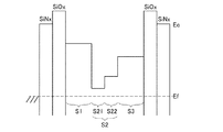
本発明の一態様に係る構成の効果を、図1を用いて以下に説明する。図1は、酸化物半導体積層のエネルギーバンド構造の一例であり、伝導帯下端(Ec)とフェルミ準位(Ef)の関係を示す。 The effect of the structure according to one embodiment of the present invention will be described below with reference to FIG. FIG. 1 is an example of an energy band structure of an oxide semiconductor stack, and shows a relationship between a conduction band lower end (Ec) and a Fermi level (Ef).
本発明の一態様のトランジスタは、ゲート絶縁層(図1では、窒化シリコン層(SiNx)と酸化シリコン層(SiOx)の積層構造)と接する第1の酸化物半導体層S1と、第1の酸化物半導体層S1上に接する第2の酸化物半導体層S2と、第2の酸化物半導体層S2上に接する第3の酸化物半導体層S3と、を含む酸化物半導体積層を有する。 The transistor of one embodiment of the present invention includes a first oxide semiconductor layer S1 in contact with a gate insulating layer (in FIG. 1, a stacked structure of a silicon nitride layer (SiNx) and a silicon oxide layer (SiOx)), a first oxide semiconductor layer S1 The oxide semiconductor stack includes a second oxide semiconductor layer S2 in contact with the physical semiconductor layer S1 and a third oxide semiconductor layer S3 in contact with the second oxide semiconductor layer S2.
酸化物半導体積層において、第1の酸化物半導体層S1と第3の酸化物半導体層S3とに挟まれた第2の酸化物半導体層S2は、第1の酸化物半導体層S1及び第3の酸化物半導体層S3よりも高い導電率σを有し、チャネルとして機能する。第2の酸化物半導体層S2は、n型不純物を含有する酸化物半導体層であり、膜厚方向においてn型不純物の濃度差を有する。図1において第2の酸化物半導体層S2は、第1の酸化物半導体層S1と接し、n型不純物を高濃度で含有する第1の領域S21と、第3の酸化物半導体層S3と接し、第1の領域S21よりもn型不純物濃度の低い第2の領域S22と、を含む。例えば、第1の領域S21をn+型の導電性を有する領域とする場合、第2の領域S22をn−型の導電性を有する領域とする。又は、第1の領域S21をn−型の導電性を有する領域として、第2の領域S22をi型の導電性を有する領域としてもよい。 In the oxide semiconductor stack, the second oxide semiconductor layer S2 sandwiched between the first oxide semiconductor layer S1 and the third oxide semiconductor layer S3 includes the first oxide semiconductor layer S1 and the third oxide semiconductor layer S1. The oxide semiconductor layer S3 has a higher conductivity σ and functions as a channel. The second oxide semiconductor layer S2 is an oxide semiconductor layer containing an n-type impurity and has a concentration difference of the n-type impurity in the film thickness direction. In FIG. 1, the second oxide semiconductor layer S2 is in contact with the first oxide semiconductor layer S1, in contact with the first region S21 containing n-type impurities at a high concentration, and the third oxide semiconductor layer S3. And a second region S22 having an n-type impurity concentration lower than that of the first region S21. For example, when the first region S21 is a region having n + -type conductivity, the second region S22 is a region having n − -type conductivity. Alternatively, the first region S21 may be a region having n − type conductivity, and the second region S22 may be a region having i type conductivity.
n型不純物を含有する第2の酸化物半導体層S2は、第1の酸化物半導体層S1及び第3の酸化物半導体層S3よりもキャリア密度が高く、第1の酸化物半導体層S1及び第3の酸化物半導体層S3と比較してフェルミ準位(Ef)が伝導帯下端(Ec)に近い位置にある。なお、図1において第2の酸化物半導体層S2は、第1の領域S21と、第2の領域S22と、を含み、第1の領域S21は、第2の領域S22よりもn型不純物を高濃度で含有する。よって、第1の領域S21は、第2の領域S22と比較してフェルミ準位(Ef)が伝導帯下端(Ec)に近い位置にある。 The second oxide semiconductor layer S2 containing an n-type impurity has a higher carrier density than the first oxide semiconductor layer S1 and the third oxide semiconductor layer S3, and the first oxide semiconductor layer S1 and the second oxide semiconductor layer S1. The Fermi level (Ef) is closer to the lower end of the conduction band (Ec) than the oxide semiconductor layer S3. Note that in FIG. 1, the second oxide semiconductor layer S2 includes a first region S21 and a second region S22, and the first region S21 contains n-type impurities more than the second region S22. Contains at high concentration. Therefore, in the first region S21, the Fermi level (Ef) is closer to the conduction band lower end (Ec) than in the second region S22.
第2の酸化物半導体層S2においてゲート絶縁層側の第1の領域S21に含まれるn型不純物を高濃度とすることで、チャネルの導電率が向上するため、トランジスタに高いオン電流特性を付与することができる。また、該第1の領域S21のバックチャネル側に第1の領域S21よりも含有n型不純物濃度の低い第2の領域S22を設けることで、トランジスタのオフ電流をより制御することが可能となり、良好なトランジスタ特性を得ることができる。 By increasing the n-type impurity contained in the first region S21 on the gate insulating layer side in the second oxide semiconductor layer S2, the conductivity of the channel is improved, so that high on-current characteristics are given to the transistor. can do. Further, by providing the second region S22 having a lower n-type impurity concentration than the first region S21 on the back channel side of the first region S21, the off-state current of the transistor can be further controlled. Good transistor characteristics can be obtained.
第1の酸化物半導体層S1及び第3の酸化物半導体層S3は、第2の酸化物半導体層S2を挟んで伝導帯下端が凹型のエネルギーバンド図を構成するように、材料、組成、結晶状態等を適宜選択する。例えば、第2の酸化物半導体層S2を構成する金属酸化物よりも導電率の小さい金属酸化物を用いて第1の酸化物半導体層S1及び/又は第3の酸化物半導体層S3を形成する。または、第1の酸化物半導体層S1及び第3の酸化物半導体層S3として、n型不純物濃度が第2の酸化物半導体層S2(より具体的には、第2の領域S22)よりも低い酸化物半導体層を適用することで伝導帯下端のエネルギー差を形成してもよく、i型(真性)または実質的にi型の酸化物半導体層を適用することが好ましい。 The first oxide semiconductor layer S1 and the third oxide semiconductor layer S3 are made of materials, compositions, and crystals so that the lower end of the conduction band forms a concave energy band diagram with the second oxide semiconductor layer S2 interposed therebetween. A state etc. are selected suitably. For example, the first oxide semiconductor layer S1 and / or the third oxide semiconductor layer S3 is formed using a metal oxide having a lower conductivity than the metal oxide that forms the second oxide semiconductor layer S2. . Alternatively, as the first oxide semiconductor layer S1 and the third oxide semiconductor layer S3, the n-type impurity concentration is lower than that of the second oxide semiconductor layer S2 (more specifically, the second region S22). The energy difference at the lower end of the conduction band may be formed by applying an oxide semiconductor layer, and it is preferable to apply an i-type (intrinsic) or substantially i-type oxide semiconductor layer.
図1に示すように、n型不純物を含有する第2の酸化物半導体層S2を挟むように、該不純物濃度が第2の酸化物半導体層S2よりも低い第1の酸化物半導体層S1及び第3の酸化物半導体層S3を設けることで、第1の酸化物半導体層S1及び第3の酸化物半導体層S3の伝導帯下端のエネルギーレベルより、第2の酸化物半導体層S2の伝導帯下端のエネルギーレベルが下がり、伝導帯下端にエネルギー差が生じる。これによって、キャリアが、酸化物半導体積層と接する絶縁層(図1では、酸化シリコン層SiOx)から離れた領域を流れる構造(いわゆる埋め込みチャネル)とすることができる。第2の酸化物半導体層S2を埋め込みチャネルとすることで、キャリアの界面散乱が低減され、高い電界効果移動度を実現することができる。 As shown in FIG. 1, the first oxide semiconductor layer S1 having an impurity concentration lower than that of the second oxide semiconductor layer S2 so as to sandwich the second oxide semiconductor layer S2 containing n-type impurities, and By providing the third oxide semiconductor layer S3, the conduction band of the second oxide semiconductor layer S2 is lower than the energy level at the lower end of the conduction band of the first oxide semiconductor layer S1 and the third oxide semiconductor layer S3. The energy level at the lower end decreases and an energy difference occurs at the lower end of the conduction band. Thus, a structure in which carriers flow in a region away from an insulating layer (in FIG. 1, a silicon oxide layer SiOx) in contact with the oxide semiconductor stack can be formed (a so-called buried channel). By using the second oxide semiconductor layer S2 as a buried channel, carrier interface scattering is reduced, and high field-effect mobility can be realized.
また、酸化物半導体積層の上層又は下層に接する絶縁層と、チャネルとの界面を安定化することができ、チャネル側界面及びバックチャネル側界面に形成されうるトラップ準位の影響を低減することができる。チャネル側界面でのトラップ準位の影響を低減することで、トランジスタの劣化、特に光負バイアス劣化等の光劣化を防止し、信頼性の高いトランジスタとすることができる。また、バックチャネル側界面におけるトラップ準位の影響を低減することで、トランジスタのしきい値電圧を制御することができる。 In addition, the interface between the insulating layer in contact with the upper layer or the lower layer of the oxide semiconductor stack and the channel can be stabilized, and the influence of trap levels that can be formed at the channel side interface and the back channel side interface can be reduced. it can. By reducing the influence of the trap level at the channel side interface, deterioration of the transistor, in particular, light deterioration such as light negative bias deterioration can be prevented and a highly reliable transistor can be obtained. Further, the threshold voltage of the transistor can be controlled by reducing the influence of the trap level at the back channel side interface.
n型不純物を含有する第2の酸化物半導体層S2は、第1の酸化物半導体層S1及び第3の酸化物半導体層S3よりも導電率σが高い。従って、第2の酸化物半導体層S2をチャネルとするトランジスタは、高い電界効果移動度を実現することができる。 The second oxide semiconductor layer S2 containing an n-type impurity has a higher conductivity σ than the first oxide semiconductor layer S1 and the third oxide semiconductor layer S3. Therefore, a transistor using the second oxide semiconductor layer S2 as a channel can achieve high field-effect mobility.
なお、本発明の一態様のトランジスタに含まれる酸化物半導体積層は、n型不純物を含有し、チャネルとして機能する第2の酸化物半導体層S2を挟むように、第1の酸化物半導体層S1と第3の酸化物半導体層S3とによって伝導帯下端にエネルギー差が形成されればよい。よって、第2の酸化物半導体層S2の伝導帯下端のエネルギーレベルが、第1の酸化物半導体層S1及び第3の酸化物半導体層S3それぞれの伝導帯下端のエネルギーレベルよりも低く、伝導帯下端が凹型のエネルギーバンド図を構成する限りにおいて、図1の構成に限定されない。 Note that the oxide semiconductor stack included in the transistor of one embodiment of the present invention includes the first oxide semiconductor layer S1 so as to sandwich the second oxide semiconductor layer S2 containing an n-type impurity and functioning as a channel. And the third oxide semiconductor layer S3 may form an energy difference at the lower end of the conduction band. Therefore, the energy level at the lower end of the conduction band of the second oxide semiconductor layer S2 is lower than the energy level at the lower end of the conduction band of each of the first oxide semiconductor layer S1 and the third oxide semiconductor layer S3. As long as the lower end constitutes a concave energy band diagram, the configuration is not limited to that shown in FIG.
なお、第1の酸化物半導体層S1と第2の酸化物半導体層S2の間、又は、第3の酸化物半導体層S3と第2の酸化物半導体層S2の間に生じる伝導帯下端のエネルギー差(ビルトインポテンシャル)は、0.05eV以上であることが好ましく、0.1eV以上であることがより好ましい。 Note that the energy at the lower end of the conduction band generated between the first oxide semiconductor layer S1 and the second oxide semiconductor layer S2 or between the third oxide semiconductor layer S3 and the second oxide semiconductor layer S2 is used. The difference (built-in potential) is preferably 0.05 eV or more, and more preferably 0.1 eV or more.
第2の酸化物半導体層S2に含まれるn型不純物としては、ボロン、窒素、リン等が挙げられる。不純物を導入して第2の酸化物半導体層S2をn型化させる手段としては、例えば、第2の酸化物半導体層S2の成膜時に窒素または一酸化二窒素を含む混合雰囲気でのスパッタリング法で成膜すればよい。または、ボロン又はリンを微量に含有するスパッタリングターゲットを用いて、n型不純物を含む第2の酸化物半導体層S2を成膜してもよい。 Examples of the n-type impurity contained in the second oxide semiconductor layer S2 include boron, nitrogen, and phosphorus. As a means for introducing the impurity to make the second oxide semiconductor layer S2 n-type, for example, a sputtering method in a mixed atmosphere containing nitrogen or dinitrogen monoxide at the time of forming the second oxide semiconductor layer S2 The film may be formed by Alternatively, the second oxide semiconductor layer S2 containing an n-type impurity may be formed using a sputtering target containing a trace amount of boron or phosphorus.
第2の酸化物半導体層S2に含まれるn型不純物の濃度に濃度差(濃度勾配)をつけるには、例えば、ボロン又はリンを含有する第1のスパッタリングターゲットを用いて、第1の領域S21を形成した後に、第1のスパッタリングターゲットよりも含有するボロン又はリンの濃度の低い第2のスパッタリングターゲットを用いて、第2の領域S22を形成することで、膜厚方向にn型不純物の濃度差を有する第2の酸化物半導体層S2を形成することができる。なお、ボロン又はリンの含有濃度の異なるスパッタリングターゲットを複数用いる場合、第2の酸化物半導体層S2を形成するためのスパッタリングターゲットに含まれる金属酸化物は同一の構成元素を同じ組成で含有することが好ましい。または、ボロン又はリンを含有するスパッタリングターゲットを用い、且つ、成膜室内に窒素ガスまたは一酸化二窒素等の窒素を含有するガスを供給して、第1の領域S21を形成した後に、同じターゲットを用いて、且つ、窒素ガスまたは窒素を含有するガスの供給を停止して第2の領域S22を形成することで、膜厚方向にn型不純物の濃度差を有する第2の酸化物半導体層S2を形成してもよい。 In order to give a concentration difference (concentration gradient) to the concentration of the n-type impurity contained in the second oxide semiconductor layer S2, for example, using the first sputtering target containing boron or phosphorus, the first region S21 is used. After forming the second region S22 by using a second sputtering target having a lower boron or phosphorus concentration than the first sputtering target, the n-type impurity concentration in the film thickness direction is formed. The second oxide semiconductor layer S2 having a difference can be formed. Note that in the case where a plurality of sputtering targets having different boron or phosphorus content concentrations are used, the metal oxide contained in the sputtering target for forming the second oxide semiconductor layer S2 contains the same constituent elements in the same composition. Is preferred. Alternatively, after forming a first region S21 by using a sputtering target containing boron or phosphorus and supplying a gas containing nitrogen such as nitrogen gas or dinitrogen monoxide into the deposition chamber, the same target is formed. And by stopping the supply of nitrogen gas or nitrogen-containing gas to form the second region S22, the second oxide semiconductor layer having the n-type impurity concentration difference in the film thickness direction S2 may be formed.
第1の酸化物半導体層S1として適用可能な酸化物半導体としては、InaM1bZncOx(aは0以上2以下の実数、bは0より大きく5以下の実数、cは0以上5以下の実数、xは任意の実数)で表記される材料を用いることができる。M1としては、トランジスタの電気特性を安定化させるためのスタビライザーとしてGa、Mg、Hf、Al、Sn、Zr、La、Ce、Pr、Nd、Sm、Eu、Gd、Tb、Dy、Ho、Er、Tm、Yb、Luなどの金属元素を含む。 As an oxide semiconductor that can be used as the first oxide semiconductor layer S1, In a M1 b Zn c O x (a is a real number of 0 or more and 2 or less, b is a real number of 0 to 5 and c is 0 or more) A material represented by a real number of 5 or less, x is an arbitrary real number) can be used. As a stabilizer for stabilizing the electrical characteristics of the transistor, M1, Ga, Mg, Hf, Al, Sn, Zr, La, Ce, Pr, Nd, Sm, Eu, Gd, Tb, Dy, Ho, Er, It includes metal elements such as Tm, Yb, and Lu.
また、第2の酸化物半導体層S2として適用可能な酸化物半導体としては、IndM2eZnfOx(dは0より大きく5以下の実数、eは0以上3以下の実数、fは0より大きく5以下の実数、xは任意の正数)で表記される材料を用いることができる。M2としては、トランジスタの電気特性を安定化させるためのスタビライザーとしてGa、Mg、Hf、Al、Sn、Zr、La、Ce、Pr、Nd、Sm、Eu、Gd、Tb、Dy、Ho、Er、Tm、Yb、Luなどの金属元素を含む。 As an oxide semiconductor that can be used as the second oxide semiconductor layer S2, In d M2 e Zn f O x (d is a real number greater than 0 and less than or equal to 5, e is a real number greater than or equal to 0 and less than or equal to 3, and f is A material represented by a real number greater than 0 and 5 or less, x being an arbitrary positive number) can be used. M2 is a stabilizer for stabilizing the electrical characteristics of the transistor, such as Ga, Mg, Hf, Al, Sn, Zr, La, Ce, Pr, Nd, Sm, Eu, Gd, Tb, Dy, Ho, Er, It includes metal elements such as Tm, Yb, and Lu.
また、第3の酸化物半導体層S3として適用可能な酸化物半導体としては、IngM3hZniOx(gは0以上2以下の実数、hは0より大きく5以下の実数、iは0以上5以下の実数、xは任意の実数)で表記される材料を用いることができる。M3としては、トランジスタの電気特性を安定化させるためのスタビライザーとしてGa、Mg、Hf、Al、Sn、Zr、La、Ce、Pr、Nd、Sm、Eu、Gd、Tb、Dy、Ho、Er、Tm、Yb、Luなどの金属元素を含む。 As an oxide semiconductor applicable as the third oxide semiconductor layer S3, In g M3 h Zn i O x (g is a real number greater than or equal to 0 and less than or equal to 2, h is a real number greater than 0 and less than or equal to 5, and i is A material represented by a real number of 0 or more and 5 or less, and x is an arbitrary real number) can be used. M3 is a stabilizer for stabilizing the electrical characteristics of the transistor, such as Ga, Mg, Hf, Al, Sn, Zr, La, Ce, Pr, Nd, Sm, Eu, Gd, Tb, Dy, Ho, Er, It includes metal elements such as Tm, Yb, and Lu.
ただし、第2の酸化物半導体層S2の構成元素に対して、第1の酸化物半導体層S1の構成元素のうちの少なくとも一が同一の金属元素である。また、第2の酸化物半導体層S2の構成元素に対して、第3の酸化物半導体層S3の構成元素のうちの少なくとも一が同一の金属元素である。 However, at least one of the constituent elements of the first oxide semiconductor layer S1 is the same metal element with respect to the constituent elements of the second oxide semiconductor layer S2. In addition, at least one of the constituent elements of the third oxide semiconductor layer S3 is the same metal element as the constituent elements of the second oxide semiconductor layer S2.
本発明の一態様により、酸化物半導体を含むトランジスタにおいて、高い電界効果移動度を実現することが可能となる。 According to one embodiment of the present invention, high field-effect mobility can be achieved in a transistor including an oxide semiconductor.
また、本発明の一態様により、酸化物半導体を含むトランジスタにおいて、電気特性の変動を抑制することができ、信頼性の高い半導体装置を提供することが可能となる。 Further, according to one embodiment of the present invention, in a transistor including an oxide semiconductor, variation in electrical characteristics can be suppressed, and a highly reliable semiconductor device can be provided.
以下では、本発明の実施の形態について図面を用いて詳細に説明する。但し、本発明は以下の説明に限定されず、その形態及び詳細を様々に変更し得ることは、当業者であれば容易に理解される。従って、本発明は以下に示す実施の形態の記載内容に限定して解釈されるものではない。 Hereinafter, embodiments of the present invention will be described in detail with reference to the drawings. However, the present invention is not limited to the following description, and it is easily understood by those skilled in the art that the modes and details can be variously changed. Therefore, the present invention should not be construed as being limited to the description of the embodiments below.
なお、以下に説明する本発明の構成において、同一部分又は同様の機能を有する部分には同一の符号を異なる図面間で共通して用い、その繰り返しの説明は省略する。また、同様の機能を有する部分を指す場合には、ハッチパターンを同じくし、特に符号を付さない場合がある。 Note that in structures of the present invention described below, the same portions or portions having similar functions are denoted by the same reference numerals in different drawings, and description thereof is not repeated. In addition, when referring to a portion having a similar function, the hatch pattern may be the same, and there may be no particular reference.
なお、本明細書で説明する各図において、各構成の大きさ、膜の厚さ、又は領域は、明瞭化のために誇張されている場合がある。よって、必ずしもそのスケールに限定されない。 Note that in each drawing described in this specification, the size, the film thickness, or the region of each component is exaggerated for clarity in some cases. Therefore, it is not necessarily limited to the scale.
なお、本明細書等において、第1、第2等として付される序数詞は、便宜上用いるものであり、工程順又は積層順を示すものではない。また、本明細書等において発明を特定するための事項として固有の名称を示すものではない。 In this specification and the like, the ordinal numbers attached as the first and second are used for convenience and do not indicate the order of steps or the order of lamination. In addition, a specific name is not shown as a matter for specifying the invention in this specification and the like.
また、本明細書において、「平行」とは、二つの直線が−10°以上10°以下の角度で配置されている状態をいう。従って、−5°以上5°以下の場合も含まれる。また、「垂直」とは、二つの直線が80°以上100°以下の角度で配置されている状態をいう。従って、85°以上95°以下の場合も含まれる。 Further, in this specification, “parallel” means a state in which two straight lines are arranged at an angle of −10 ° to 10 °. Therefore, the case of −5 ° to 5 ° is also included. “Vertical” refers to a state in which two straight lines are arranged at an angle of 80 ° to 100 °. Therefore, the case of 85 ° to 95 ° is also included.
また、本明細書において、結晶が三方晶または菱面体晶である場合、六方晶系として表す。 In this specification, when a crystal is trigonal or rhombohedral, it is represented as a hexagonal system.
(実施の形態1)
本実施の形態では、半導体装置及び半導体装置の作製方法の一形態を、図2及び図3を用いて説明する。本実施の形態では、半導体装置の一例として、酸化物半導体層を有するボトムゲート型のトランジスタを示す。
(Embodiment 1)
In this embodiment, one embodiment of a semiconductor device and a method for manufacturing the semiconductor device will be described with reference to FIGS. In this embodiment, a bottom-gate transistor including an oxide semiconductor layer is described as an example of a semiconductor device.
図2にトランジスタ310の構成例を示す。図2(A)は、トランジスタ310の平面図を示し、図2(B)は、図2(A)のX1−Y1における断面図を示し、図2(C)は、図2(A)のV1−W1における断面図を示す。
FIG. 2 illustrates a configuration example of the
図2に示すトランジスタ310は、絶縁表面を有する基板400上に設けられたゲート電極層402と、ゲート電極層402上のゲート絶縁層404と、ゲート絶縁層404と接し、ゲート電極層402と重畳する酸化物半導体積層408と、酸化物半導体積層408と電気的に接続するソース電極層410a及びドレイン電極層410bと、を含む。また、ソース電極層410a及びドレイン電極層410bを覆い、酸化物半導体積層408と接する絶縁層412をトランジスタ310の構成要素としてもよい。トランジスタ310のチャネル長は、例えば1μm以上とすることができる。
2 includes a
本実施の形態において、ゲート絶縁層404は、ゲート電極層402と接するゲート絶縁層404aと、ゲート絶縁層404a上に設けられ、酸化物半導体積層408と接するゲート絶縁層404bの積層構造とする。また、絶縁層412は、ソース電極層410a及びドレイン電極層410bと接する絶縁層412aと、絶縁層412a上の絶縁層412bの積層構造とする。
In this embodiment, the
酸化物半導体積層408は、ゲート絶縁層404に接する第1の酸化物半導体層408aと、第1の酸化物半導体層408a上に接する第2の酸化物半導体層408bと、第2の酸化物半導体層408b上に接し、ソース電極層410a及びドレイン電極層410bと接する第3の酸化物半導体層408cと、を含む。第3の酸化物半導体層408cは、第1の酸化物半導体層408aの側面及び第2の酸化物半導体層408bの側面を覆って設けられている。また、第3の酸化物半導体層408cの周縁部は、ゲート絶縁層404と接する。
The
なお、第2の酸化物半導体層408bとしては、n型の導電性を付与する不純物(n型不純物)を含有する酸化物半導体層を適用する。第2の酸化物半導体層408bは、膜厚方向にn型不純物の濃度差を有しており、第2の酸化物半導体層408bにおいて第1の酸化物半導体層408aと接する領域は、第3の酸化物半導体層408cと接する領域よりも高濃度でn型不純物を含有する。本実施の形態においては、第2の酸化物半導体層408bは、第1の酸化物半導体層408aと接し、n型不純物を高濃度で含む(例えば、n+型の導電性を有する)第1の領域408b1と、第3の酸化物半導体層408cと接し、第1の領域408b1よりも低濃度でn型不純物を含む(例えば、n−型の導電性を有する)第2の領域408b2と、を有する。但し、本発明の実施の形態はこれに限られず、第1の酸化物半導体層408aと接する領域から第3の酸化物半導体層408cと接する領域に連続的にn型不純物濃度が減少するように、濃度勾配を有する第2の酸化物半導体層408bとしてもよい。
Note that as the second
第1の酸化物半導体層408a及び第3の酸化物半導体層408cとしては、第2の酸化物半導体層408bを挟んで伝導帯下端が凹型のエネルギーバンド図を構成するように、材料、組成、結晶構造等を適宜選択する。例えば、第2の酸化物半導体層408bを構成する金属酸化物よりも導電率の小さい金属酸化物を用いて第1の酸化物半導体層408a及び/又は第3の酸化物半導体層408cを形成する。酸化物半導体層の構成元素が同一の場合には、より大きいバンドギャップを有する組成を選択して第1の酸化物半導体層408a及び/又は第3の酸化物半導体層408cを形成すればよい。または、第1の酸化物半導体層408a及び第3の酸化物半導体層408cとして、n型不純物濃度が第2の酸化物半導体層408b(より具体的には、第2の領域408b2)よりも低い酸化物半導体層を適用することで伝導帯下端のエネルギー差を形成してもよく、i型(真性)または実質的にi型の酸化物半導体層を適用することが好ましい。
As the first
なお、n型不純物を含有する第2の酸化物半導体層408bは、第1の酸化物半導体層408a及び第3の酸化物半導体層408cより導電率σが高い。第2の酸化物半導体層408bの導電率σを高めると、第2の酸化物半導体層408bとドレイン電極層410bとの距離(第3の酸化物半導体層408cの膜厚)が支配的となり、見かけ上、順方向に対してはチャネル長が短縮されたと見なせる。よって、トランジスタのオン特性を向上することができる。また、逆方向に対しては、第3の酸化物半導体層408cは空乏化して十分に低いオフ電流を期待することができる。
Note that the second
酸化物半導体積層408において、チャネルとして機能する第2の酸化物半導体層408bにn型不純物を含有させることで、チャネルのキャリア密度を高めることができ、エネルギーバンド図におけるフェルミ準位(Ef)が伝導帯側に近づく。この結果、トランジスタの電界効果移動度を向上させることができる。
In the
また、第2の酸化物半導体層408bとしてn型不純物を含む酸化物半導体層を用い、第1の酸化物半導体層408a及び第3の酸化物半導体層408cと、第2の酸化物半導体層408bとの間に伝導帯下端のエネルギー差が形成されるように、酸化物半導体積層を構成する。例えば、第2の酸化物半導体層408bを挟む第1の酸化物半導体層408a及び第3の酸化物半導体層408cのn型不純物濃度を第2の酸化物半導体層408bより低く、好ましくはi型とする。チャネルとして機能する第2の酸化物半導体層408bと、第1の酸化物半導体層408a及び第3の酸化物半導体層408cとの間に伝導帯下端のエネルギー差を有することで、キャリアが酸化物半導体積層408と接する絶縁層(ゲート絶縁層404及び/又は絶縁層412)から離れた領域を流れる構造(埋め込みチャネル)とすることができる。第2の酸化物半導体層408bを埋め込みチャネルとすることで、キャリアの界面散乱が低減され、高い電界効果移動度を実現することができる。
In addition, an oxide semiconductor layer containing an n-type impurity is used as the second
さらに第2の酸化物半導体層408bのうちゲート絶縁層側の第1の領域408b1が、バックチャネル側の第2の領域408b2よりも高濃度でn型不純物を有することで、トランジスタのオン特性(例えば、オン電流、電界効果移動度)の向上を図りながら、オフ電流を制御することができる。
Further, in the second
第1の酸化物半導体層408aと第2の酸化物半導体層408bの第1の領域408b1との間、及び、第3の酸化物半導体層408cと第2の酸化物半導体層408bの第2の領域408b2との間に生じる伝導帯下端のエネルギー差(ビルトインポテンシャル)は、0.05eV以上であることが好ましく、0.1eV以上であることがより好ましい。
Between the first region 408b1 of the first
第1の酸化物半導体層408aを設けて、チャネルとゲート絶縁層との界面でのキャリアの捕獲を抑制することで、トランジスタの光劣化(例えば、光負バイアス劣化)を低減することができ、信頼性の高いトランジスタを得ることができる。
By providing the first
なお、一般的に、酸化物半導体層は、スパッタリング法を用いて成膜されることが多い。一方で、酸化物半導体層のスパッタリングの際にイオン化された希ガス元素(例えば、アルゴン)や、スパッタリングターゲット表面からはじき飛ばされた元素が、ゲート絶縁層などの酸化物半導体層の被形成面となる膜の構成元素をはじき飛ばしてしまうことがある。このようにして被形成面となる膜からはじき飛ばされた元素は、酸化物半導体層に不純物元素として取り込まれてしまい、特に酸化物半導体層の被形成面近傍には、不純物元素が高い濃度で取り込まれる恐れがある。又、不純物元素が酸化物半導体層の被形成面近傍に残存すると、当該酸化物半導体層が高抵抗化してしまい、トランジスタの電気特性の低下の要因となる。 Note that in general, an oxide semiconductor layer is often formed by a sputtering method. On the other hand, a rare gas element (for example, argon) ionized at the time of sputtering of the oxide semiconductor layer or an element blown off from the surface of the sputtering target becomes a formation surface of the oxide semiconductor layer such as a gate insulating layer. The constituent elements of the film may be repelled. The element thus blown off from the film to be the formation surface is taken in as an impurity element into the oxide semiconductor layer, and in particular, the impurity element is taken in at a high concentration near the formation surface of the oxide semiconductor layer. There is a fear. In addition, when the impurity element remains in the vicinity of the formation surface of the oxide semiconductor layer, the resistance of the oxide semiconductor layer is increased, which causes a reduction in electrical characteristics of the transistor.
しかしながら、トランジスタ310においては、チャネルが形成される第2の酸化物半導体層408bと、ゲート絶縁層404との間に第1の酸化物半導体層408aを有することで、ゲート絶縁層404の構成元素がチャネルまで拡散することを抑制することができる。すなわち、第1の酸化物半導体層408aは、ゲート絶縁層404の構成元素(例えば、シリコン)を不純物として含む場合がある。第1の酸化物半導体層408aを含むことで、トランジスタ310の電気特性をより安定化することができ、信頼性の高い半導体装置を提供することができる。
However, in the
また、第2の酸化物半導体層408bのバックチャネル側に設けられた第3の酸化物半導体層408cは、トランジスタ310のバックチャネル側界面におけるトラップ準位の影響を低減する。例えば、第3の酸化物半導体層408cはソース電極層410a及びドレイン電極層410bの構成元素が第2の酸化物半導体層408bへと拡散することを防止することができる。すなわち、第3の酸化物半導体層408cは、ソース電極層410a及びドレイン電極層410bの構成元素(例えば、銅)を不純物として含むことがある。第3の酸化物半導体層408cを設けることで、トランジスタのチャネルにおいてトラップ準位が形成されることを抑制することができるため、トラップ準位に起因するS値の増大の抑制、及び/又は、しきい値電圧の制御を可能とすることができる。第3の酸化物半導体層408cによってしきい値電圧を制御することで、ノーマリオフのトランジスタを実現することができる。
In addition, the third
チャネル側界面のトラップ準位の影響を低減し、トランジスタの電気特性を安定化させる第1の酸化物半導体層408aの膜厚は、例えば、3nm以上20nm以下、又は5nm以上10nm以下とすることできる。第1の酸化物半導体層408aを上述の膜厚で設けることで、第1の酸化物半導体層408aに、ゲート絶縁層404の構成元素が不純物として含有した場合であっても、該不純物がチャネルとして機能する第2の酸化物半導体層408bへと達することを抑制することができる。また、チャネルとして機能する第2の酸化物半導体層408bの膜厚(第1の領域408b1と第2の領域408b2の総厚)は、10nm以上40nm以下とすることが好ましく、15nm以上30nm以下とすることがより好ましい。また、バックチャネル側界面のトラップ準位の影響を低減し、しきい値電圧の制御を可能とする第3の酸化物半導体層408cの膜厚は、例えば、10nm以上40nm以下、又は、15nm以上30nm以下とすることができる。
The thickness of the first
なお、上述したように、第3の酸化物半導体層408cの膜厚は、トランジスタ310の実質的なチャネル長となりうる。よって、ノーマリオフのトランジスタを実現するためには、第3の酸化物半導体層408cの膜厚は厚いことが好ましい。また、ゲート絶縁層404と接する第1の酸化物半導体層408aの膜厚が厚すぎると、電流が第1の酸化物半導体層408a中又は界面を流れてしまうことがある。よって、第1の酸化物半導体層408aの膜厚は、第2の酸化物半導体層408bの膜厚よりも小さく、第3の酸化物半導体層408cの膜厚は、第2の酸化物半導体層408bの膜厚以上であることが好ましい。
Note that as described above, the thickness of the third
第1の酸化物半導体層408a乃至第3の酸化物半導体層408cは、構成元素の異なる酸化物半導体を用いてもよいし、構成元素を同一とし、組成を異ならせてもよい。但し、トランジスタ310のチャネルとして機能する第2の酸化物半導体層408bとしては、電界効果移動度の高い酸化物半導体を適用することが好ましい。
For the first
例えば、第1の酸化物半導体層408a乃至第3の酸化物半導体層408cとしてインジウム及びガリウムを含有する酸化物半導体を用いる場合、第2の酸化物半導体層408bとしてインジウムの組成がガリウムの組成よりも大きい酸化物半導体を用いることが好ましく、第1の酸化物半導体層408a及び第3の酸化物半導体層408cとしては、インジウムの組成がガリウムの組成以下である酸化物半導体を用いることが好ましい。
For example, in the case where an oxide semiconductor containing indium and gallium is used for the first
酸化物半導体では、主として重金属のs軌道がキャリア伝導に寄与しており、インジウムの含有率を多くすることによりs軌道のオーバーラップが多くなる傾向がある。よって、第2の酸化物半導体層408bにおいて、インジウムの組成をガリウムの組成よりも大きくすることで、インジウムの組成がガリウムの組成以下である酸化物と比較して高い電界効果移動度を備えることが可能となる。
In oxide semiconductors, s orbitals of heavy metals mainly contribute to carrier conduction, and there is a tendency that s orbital overlap increases by increasing the indium content. Therefore, the second
また、他の金属元素に対するガリウムの割合が大きいほど、エネルギーギャップの大きい金属酸化物となるため、インジウムの組成をガリウムの組成以下とすることで、第1の酸化物半導体層408a、第3の酸化物半導体層408cは第2の酸化物半導体層408bよりも大きなエネルギーギャップを有する。よって、第2の酸化物半導体層408bと第1の酸化物半導体層408a、第3の酸化物半導体層408cとの間に効果的に伝導帯下端のエネルギー差を形成するため好ましい。また、ガリウムはインジウムと比較して酸素欠損の形成エネルギーが大きく酸素欠損が生じにくいため、インジウムの組成がガリウムの組成以下である金属酸化物はインジウムの組成がガリウムの組成より大きい金属酸化物と比較して安定した特性を備える。よって、トランジスタ310のバックチャネル側をより安定化することが可能となる。なお、第1の酸化物半導体層408a及び/又は第3の酸化物半導体層408cとして、酸化ガリウム、又は酸化亜鉛ガリウムを用いてもよい。
Further, the larger the ratio of gallium to the other metal elements, the larger the energy gap, and thus the metal oxide becomes larger. Therefore, by setting the composition of indium to be equal to or less than the composition of gallium, the first
例えば、第1の酸化物半導体層408a乃至第3の酸化物半導体層408cとして、In−Ga−Zn系酸化物半導体を用いる場合、第1の酸化物半導体層408a又は第3の酸化物半導体層408cには、In:Ga:Zn=1:1:1(=1/3:1/3:1/3)、In:Ga:Zn=1:3:2(=1/6:3/6:2/6)、In:Ga:Zn=2:4:3(=2/9:4/9:3/9)、あるいはIn:Ga:Zn=1:5:3(=1/9:5/9:3/9)の組成(原子数比)のIn−Ga−Zn系酸化物やその組成の近傍の金属酸化物を用いることが好ましい。第2の酸化物半導体層408bには、In:Ga:Zn=3:1:2(=3/6:1/6:2/6)、In:Ga:Zn=4:2:3(=4/9:2/9:3/9)、In:Ga:Zn=5:1:3(=5/9:1/9:3/9)、In:Ga:Zn=5:3:4(=5/12:3/12:4/12)、In:Ga:Zn=6:2:4(=6/12:2/12:4/12)、あるいはIn:Ga:Zn=7:1:3(=7/11:1/11:3/11)の組成(原子数比)のIn−Ga−Zn系酸化物やその組成の近傍の金属酸化物を用いることが好ましい。
For example, in the case where an In—Ga—Zn-based oxide semiconductor is used for the first
なお、例えば、In、Ga、Znの組成がIn:Ga:Zn=a:b:c(a+b+c=1)である酸化物の組成が、組成がIn:Ga:Zn=A:B:C(A+B+C=1)の酸化物の組成の近傍であるとは、a、b、cが、(a−A)2+(b−B)2+(c−C)2≦r2を満たすことをいう。rとしては、例えば、0.05とすればよい。 Note that for example, the composition of an oxide whose composition of In, Ga, and Zn is In: Ga: Zn = a: b: c (a + b + c = 1) is the same as the composition of In: Ga: Zn = A: B: C ( “A + B + C = 1) being in the vicinity of the oxide composition means that a, b and c satisfy (a−A) 2 + (b−B) 2 + (c−C) 2 ≦ r 2. Say. For example, r may be 0.05.
本実施の形態においては、第1の酸化物半導体層408aとして、In:Ga:Zn=1:3:2の組成(原子数比)のIn−Ga−Zn系酸化物を用い、第2の酸化物半導体層408bとして、In:Ga:Zn=3:1:2の組成(原子数比)のIn−Ga−Zn系酸化物を用い、第3の酸化物半導体層408cとして、In:Ga:Zn=1:1:1の組成(原子数比)のIn−Ga−Zn系酸化物を用いるものとする。
In this embodiment, an In—Ga—Zn-based oxide having a composition (atomic ratio) of In: Ga: Zn = 1: 3: 2 is used as the first
なお、酸化物半導体積層408に適用する酸化物半導体としては、これらに限られず、必要とする電気的特性(電界効果移動度、しきい値、ばらつき等)に応じて適切な組成のものを用いればよい。また、必要とする電気的特性を得るために、キャリア濃度や不純物濃度、欠陥密度、金属元素と酸素の原子数比、原子間距離、密度等を適切なものとすることが好ましい。
Note that the oxide semiconductor used for the
例えば、トランジスタの電気特性のばらつきを減らすためのスタビライザーとして、ガリウム(Ga)に代えて、又はガリウム(Ga)に加えて、スズ(Sn)、ハフニウム(Hf)、アルミニウム(Al)、ジルコニウム(Zr)のいずれか一種または複数種を有していてもよい。また、他のスタビライザーとして、ランタノイドである、ランタン(La)、セリウム(Ce)、プラセオジム(Pr)、ネオジム(Nd)、サマリウム(Sm)、ユウロピウム(Eu)、ガドリニウム(Gd)、テルビウム(Tb)、ジスプロシウム(Dy)、ホルミウム(Ho)、エルビウム(Er)、ツリウム(Tm)、イッテルビウム(Yb)、ルテチウム(Lu)のいずれか一種または複数種を有してもよい。 For example, as a stabilizer for reducing variation in electrical characteristics of transistors, tin (Sn), hafnium (Hf), aluminum (Al), zirconium (Zr) instead of gallium (Ga) or in addition to gallium (Ga) 1 type or multiple types may be included. As other stabilizers, lanthanoids such as lanthanum (La), cerium (Ce), praseodymium (Pr), neodymium (Nd), samarium (Sm), europium (Eu), gadolinium (Gd), terbium (Tb) , Dysprosium (Dy), holmium (Ho), erbium (Er), thulium (Tm), ytterbium (Yb), or lutetium (Lu).
酸化物半導体層は、スパッタリング法によって形成することができ、スパッタリングターゲットにインジウムを含有すると成膜時のパーティクルの発生を低減することができる。よって、インジウムを含む酸化物半導体層を適用することがより好ましい。 The oxide semiconductor layer can be formed by a sputtering method. When indium is contained in the sputtering target, generation of particles during film formation can be reduced. Therefore, it is more preferable to use an oxide semiconductor layer containing indium.
なお、第1の酸化物半導体層408a乃至第3の酸化物半導体層408cの構成元素は、少なくとも一つが共通する。このとき、材料や成膜条件によっては、各酸化物半導体層同士の界面が不明確になる場合もある。また、同様に、第2の酸化物半導体層408bにおいて、第1の領域408b1及び第2の領域408b2は、酸化物半導体の構成元素及びその組成が同一であり、n型不純物濃度が異なるため、領域同士の界面が不明確となる場合もある。図2においては、第1の領域408b1と第2の領域408b2の界面が不明確な場合として、該界面を模式的に点線で図示している。これは以降の各図面においても同様である。
Note that at least one of the constituent elements of the first
以下に、図3を用いてトランジスタ310の作製方法の一例を示す。
An example of a method for manufacturing the
まず、絶縁表面を有する基板400上に、ゲート電極層402(これと同じ層で形成される配線を含む)を形成する。
First, the gate electrode layer 402 (including a wiring formed using the same layer) is formed over the
絶縁表面を有する基板400に使用することができる基板に大きな制約はないが、少なくとも後の熱処理に耐えられる程度の耐熱性を有することが必要となる。例えば、バリウムホウケイ酸ガラスやアルミノホウケイ酸ガラス等のガラス基板、セラミック基板、石英基板、サファイヤ基板などを用いることができる。また、シリコンや炭化シリコン等の単結晶半導体基板、多結晶半導体基板、シリコンゲルマニウム等の化合物半導体基板、SOI基板等を適用することができ、これらの基板に半導体素子が設けられたものを基板400として用いてもよい。また、基板400上に下地絶縁層を形成してもよい。
There is no particular limitation on a substrate that can be used as the
ゲート電極層402の材料は、モリブデン、チタン、タンタル、タングステン、アルミニウム、銅、クロム、ネオジム、スカンジウム等の金属材料又はこれらを主成分とする合金材料を用いて形成することができる。また、ゲート電極層402としてリン等の不純物元素をドーピングした多結晶シリコン膜に代表される半導体膜、ニッケルシリサイド等のシリサイド膜を用いてもよい。ゲート電極層402は単層構造としてもよいし、積層構造としてもよい。ゲート電極層402はテーパ形状としてもよく、例えばテーパ角を15°以上70°以下とすればよい。ここで、テーパ角とは、テーパ形状を有する層の側面と、当該層の底面との間の角度を指す。
The material of the
また、ゲート電極層402の材料は、酸化インジウム酸化スズ、酸化タングステンを含むインジウム酸化物、酸化タングステンを含むインジウム亜鉛酸化物、酸化チタンを含むインジウム酸化物、酸化チタンを含むインジウムスズ酸化物、酸化インジウム酸化亜鉛、酸化ケイ素を添加したインジウムスズ酸化物等の導電性材料を適用することもできる。
The material of the
または、ゲート電極層402の材料として、窒素を含むIn−Ga−Zn系酸化物、窒素を含むIn−Sn系酸化物、窒素を含むIn−Ga系酸化物、窒素を含むIn−Zn系酸化物、窒素を含むSn系酸化物、窒素を含むIn系酸化物、金属窒化物膜(窒化インジウム膜、窒化亜鉛膜、窒化タンタル膜、窒化タングステン膜など)を用いてもよい。これらの材料は、5eV以上の仕事関数を有するため、これらの材料を用いてゲート電極層402を形成することでトランジスタのしきい値電圧をプラスにすることができ、ノーマリオフのスイッチングトランジスタを実現できる。
Alternatively, as a material of the
次いで、ゲート電極層402を覆うようにゲート電極層402上にゲート絶縁層404を形成する(図3(A)参照)。ゲート絶縁層404としては、プラズマCVD法、スパッタリング法等により、酸化シリコン膜、酸化窒化シリコン膜、窒化酸化シリコン膜、窒化シリコン膜、酸化アルミニウム膜、酸化ハフニウム膜、酸化イットリウム膜、酸化ジルコニウム膜、酸化ガリウム膜、酸化タンタル膜、酸化マグネシウム膜、酸化ランタン膜、酸化セリウム膜および酸化ネオジム膜を一種以上含む絶縁膜を、単層で、または積層で用いる。
Next, a
なお、ゲート絶縁層404において、後に形成される第1の酸化物半導体層408aと接する領域(本実施の形態においては、ゲート絶縁層404b)は、酸化物絶縁層であることが好ましく、化学量論的組成よりも過剰に酸素を含有する領域(酸素過剰領域)を有することがより好ましい。ゲート絶縁層404に酸素過剰領域を設けるには、例えば、酸素雰囲気下にてゲート絶縁層404を形成すればよい。又は、成膜後のゲート絶縁層404に酸素を導入して、酸素過剰領域を形成してもよい。酸素の導入方法としては、イオン注入法、イオンドーピング法、プラズマイマージョンイオン注入法、プラズマ処理等を用いることができる。
Note that a region in the
本実施の形態では、ゲート絶縁層404aとして窒化シリコン膜を形成し、ゲート絶縁層404bとして酸化シリコン膜を形成する。
In this embodiment, a silicon nitride film is formed as the
次いで、ゲート絶縁層404上に、酸化物半導体膜407aを成膜する。
Next, the
酸化物半導体膜407aの成膜方法は、スパッタリング法、MBE(Molecular Beam Epitaxy)法、CVD法、パルスレーザ堆積法、ALD(Atomic Layer Deposition)法等を適宜用いることができる。
As a method for forming the
なお、ゲート絶縁層404及び酸化物半導体膜407aは、大気開放せずに連続的に成膜することが好ましい。ゲート絶縁層404及び酸化物半導体膜407aの成膜を大気開放せずに連続的に行うことで、酸化物半導体膜407a表面への水素又は水素化合物の付着(例えば、吸着水など)を防止することができるため、不純物の混入を抑制することができる。
Note that the
酸化物半導体膜を成膜するためのスパッタリングターゲットは多結晶、且つ、相対密度(充填率)の高いものを用いる。また、成膜時のスパッタリングターゲットは十分冷やして室温とし、被成膜基板の被成膜面は、室温以上に高め、成膜室内に水分や水素がほとんどない雰囲気下で酸化物半導体膜の成膜を行う。 As the sputtering target for forming the oxide semiconductor film, a polycrystalline target having a high relative density (filling rate) is used. In addition, the sputtering target at the time of film formation is sufficiently cooled to room temperature, the film formation surface of the film formation substrate is raised to room temperature or higher, and the oxide semiconductor film is formed in an atmosphere with little moisture or hydrogen in the film formation chamber. Do the membrane.
スパッタリングターゲットは高密度であるほど好ましい。スパッタリングターゲットの密度が高いことで成膜される膜密度も高くすることができる。具体的には、ターゲットの相対密度(充填率)は90%以上100%以下、好ましくは95%以上、さらに好ましくは99.9%以上とする。なお、スパッタリングターゲットの相対密度とは、スパッタリングターゲットと同一組成の材料の気孔のない状態における密度との比をいう。 The higher the density of the sputtering target, the better. Since the density of the sputtering target is high, the density of the film formed can also be increased. Specifically, the relative density (filling rate) of the target is 90% or more and 100% or less, preferably 95% or more, and more preferably 99.9% or more. Note that the relative density of the sputtering target refers to the ratio of the material having the same composition as the sputtering target to the density without pores.
スパッタリングターゲットは、不活性ガス雰囲気(窒素または希ガス雰囲気)下、真空中または高圧雰囲気中で焼成を行うことが好ましい。焼成方法として常圧焼成法、加圧焼成法等を適宜用いて得られる多結晶ターゲットを用いる。加圧焼成法としては、ホットプレス法、熱間等方加圧(HIP:Hot Isostatic Pressing)法、放電プラズマ焼結法、又は衝撃法を適用することが好ましい。焼成の最高温度はスパッタリングターゲット材料の焼結温度により選択するが、1000℃〜2000℃程度とするのが好ましく、1200℃〜1500℃とするのがより好ましい。また、最高温度の保持時間は、スパッタリングターゲット材料により選択するが、0.5時間〜3時間とするのが好ましい。 The sputtering target is preferably baked in an inert gas atmosphere (nitrogen or rare gas atmosphere) in a vacuum or in a high pressure atmosphere. A polycrystalline target obtained by appropriately using a normal pressure firing method, a pressure firing method or the like as the firing method is used. As the pressure firing method, it is preferable to apply a hot pressing method, a hot isostatic pressing (HIP) method, a discharge plasma sintering method, or an impact method. Although the maximum temperature of baking is selected by the sintering temperature of sputtering target material, it is preferable to set it as about 1000 to 2000 degreeC, and it is more preferable to set it as 1200 to 1500 degreeC. The maximum temperature holding time is selected according to the sputtering target material, but is preferably 0.5 hours to 3 hours.
In−Ga−Zn系酸化物膜を成膜する場合、スパッタリングターゲットは、In:Ga:Zn=3:1:2の原子数比のターゲットや、In:Ga:Zn=1:1:1の原子数比のターゲットを用いる。例えば、本実施の形態では、In:Ga:Zn=1:3:2の原子数比のターゲットを用いて、酸化物半導体膜407aを成膜する。また、酸化物半導体膜407bの成膜には、In:Ga:Zn=3:1:2の原子数比のターゲットを用い、酸化物半導体膜407cの成膜には、In:Ga:Zn=1:1:1の原子数比のターゲットを用いる。
In the case where an In—Ga—Zn-based oxide film is formed, a sputtering target can be an In: Ga: Zn = 3: 1: 2 atomic ratio target or an In: Ga: Zn = 1: 1: 1 target. An atomic ratio target is used. For example, in this embodiment, the
また、成膜チャンバー内に残存する不純物を低減することも緻密な膜を得る上で重要である。成膜チャンバー内の背圧(到達真空度:反応ガスを導入する前の真空度)を5×10⁻³Pa以下、好ましくは6×10⁻⁵Pa以下とし、成膜時の圧力を2Pa未満、好ましくは0.4Pa以下とする。背圧を低くすることで成膜チャンバー内の不純物を低減する。 In addition, it is important to reduce impurities remaining in the deposition chamber in order to obtain a dense film. The back pressure in the film forming chamber (degree of ultimate vacuum: degree of vacuum before introducing the reaction gas) is 5 × 10 −3 Pa or less, preferably 6 × 10 −5 Pa or less, and the pressure during film formation is less than 2 Pa. , Preferably 0.4 Pa or less. Impurities in the deposition chamber are reduced by lowering the back pressure.
また、成膜チャンバー内に導入するガス、即ち、成膜時に用いるガス中の不純物を低減することも緻密な膜を得る上で重要である。また、成膜ガス中の酸素割合を高め、電力を最適化することが重要である。成膜ガス中の酸素割合(上限は酸素100%)を高め、電力を最適化することによって成膜時のプラズマダメージを軽減することができる。そのため、緻密な膜を得やすくなる。 In addition, it is important to reduce impurities in a gas introduced into the film formation chamber, that is, a gas used in film formation, in order to obtain a dense film. In addition, it is important to increase the oxygen ratio in the deposition gas and optimize the power. Plasma damage during film formation can be reduced by increasing the oxygen ratio in the film formation gas (the upper limit is 100% oxygen) and optimizing the power. Therefore, it becomes easy to obtain a dense film.
また、酸化物半導体膜の成膜前または成膜中には成膜チャンバー内の水分量などを監視(モニター)するため、四重極形質量分析計(以下、Q−massと呼ぶ)を常に作動させた状態で成膜を行うことが好ましい。 In addition, a quadrupole mass spectrometer (hereinafter referred to as Q-mass) is always used to monitor the amount of moisture in the deposition chamber before or during the formation of the oxide semiconductor film. It is preferable to perform film formation in the operated state.
例えば、スパッタリング法を用いて酸化物半導体膜407aの成膜を行う場合には、スパッタリング装置の成膜室内に供給する成膜ガスとして、水素、水、水酸基又は水素化物などの不純物が除去された高純度の希ガスと酸素の混合ガス、又は酸素を用いる。
For example, in the case where the
なお、成膜後の酸化物半導体膜407aに、脱水化又は脱水素化処理のための熱処理を適宜行ってもよい。また、脱水化又は脱水素化処理を行った酸化物半導体膜407aに、酸素を供給してもよい。
Note that heat treatment for dehydration or dehydrogenation treatment may be appropriately performed on the
次いで、酸化物半導体膜407a上に接して、n型不純物を含有し、膜厚方向において該n型不純物濃度が濃度差を有する酸化物半導体膜407bを成膜する(図3(B)参照)。酸化物半導体膜407bの成膜は、酸化物半導体膜407aとは、別の成膜室内にて行うことが好ましい。例えば、成膜室内に供給する成膜ガスとして、酸化物半導体膜407aで示した成膜ガスに、窒素ガス、又は一酸化二窒素ガス等の窒素を含むガスを混合して供給することで、n型不純物を含有する酸化物半導体膜407bの第1の領域407b1を成膜する。その後、同じ成膜室内にて窒素ガス、又は一酸化二窒素ガス等の窒素を含むガスの流量比を低減させて、第1の領域407b1よりもn型不純物濃度の低い酸化物半導体膜407bの第2の領域407b2を形成する。酸化物半導体膜407bのその他の成膜条件は、酸化物半導体膜407aと同様とすることができる。
Next, an
次いで、積層した酸化物半導体膜407a及び酸化物半導体膜407bを、フォトリソグラフィ法を用いたエッチング処理によって島状の第1の酸化物半導体層408a及び第2の酸化物半導体層408bに加工する。その後、島状の第1の酸化物半導体層408a及び第2の酸化物半導体層408bを覆うように、酸化物半導体膜407cを成膜する(図3(C)参照)。酸化物半導体膜407cの成膜は、酸化物半導体膜407aと同じ成膜室を用いて成膜してもよい。酸化物半導体膜407cの成膜条件は、酸化物半導体膜407aと同様とすることができる。
Next, the stacked
次いで、酸化物半導体膜407cを、フォトリソグラフィ法を用いたエッチング処理によって島状の第3の酸化物半導体層408cに加工して、酸化物半導体積層408を形成する(図3(D)参照)。第3の酸化物半導体層408cは、第1の酸化物半導体層408a及び第2の酸化物半導体層408bの側面を覆うように、第2の酸化物半導体層408b上に接して設けられる。
Next, the
次いで、酸化物半導体積層408上に導電膜を形成し、これを加工してソース電極層410a及びドレイン電極層410b(これと同じ層で形成される配線を含む)を形成する。
Next, a conductive film is formed over the
ソース電極層410a及びドレイン電極層410bとしては、例えば、Al、Cr、Cu、Ta、Ti、Mo、Wから選ばれた元素を含む金属膜、または上述した元素を成分とする金属窒化物膜(窒化チタン膜、窒化モリブデン膜、窒化タングステン膜)等を用いることができる。また、Al、Cuなどの金属膜の下側又は上側の一方または双方にTi、Mo、Wなどの高融点金属膜またはそれらの金属窒化物膜(窒化チタン膜、窒化モリブデン膜、窒化タングステン膜)を積層させた構成としてもよい。また、ソース電極層410a及びドレイン電極層410bを、導電性の金属酸化物で形成してもよい。導電性の金属酸化物としては酸化インジウム(In2O3)、酸化スズ(SnO2)、酸化亜鉛(ZnO)、酸化インジウム酸化スズ(In2O3−SnO2)、酸化インジウム酸化亜鉛(In2O3−ZnO)またはこれらの金属酸化物材料に酸化シリコンを含ませたものを用いることができる。
As the
また、ソース電極層410a及びドレイン電極層410bとして窒素を含むIn−Ga−Zn−O膜、窒素を含むIn−Sn−O膜、窒素を含むIn−Ga−O膜、窒素を含むIn−Zn−O膜、窒素を含むSn−O膜、窒素を含むIn−O膜等の金属窒化物膜を用いることができる。これらの膜は、酸化物半導体積層408と同じ構成元素を含むため、酸化物半導体積層408との界面を安定化させることができる。
In addition, as the
次いで、ソース電極層410a、ドレイン電極層410b及び露出した酸化物半導体積層408を覆うように、絶縁層412を形成する(図3(E)参照)。
Next, an insulating
絶縁層412としてはプラズマCVD法、スパッタリング法により形成することができ、酸化シリコン膜、酸化ガリウム膜、酸化アルミニウム膜、窒化シリコン膜、酸化窒化シリコン膜、酸化窒化アルミニウム膜、または窒化酸化シリコン膜等を単層で、又は積層して用いることができる。但し、酸化物半導体積層408と接する絶縁層412(本実施の形態においては、絶縁層412a)として、酸化物絶縁層を形成すると、該酸化物絶縁層によって酸化物半導体積層408へ酸素を供給することが可能となるため、好ましい。
The insulating
例えば、プラズマCVD装置の真空排気された処理室内に載置された基板を180℃以上400℃以下、さらに好ましくは200℃以上370℃以下に保持し、処理室に原料ガスを導入して処理室内における圧力を30Pa以上250Pa以下、さらに好ましくは40Pa以上200Pa以下とし、処理室内に設けられる電極に高周波電力を供給する条件により、酸化シリコン膜または酸化窒化シリコン膜を形成してもよい。上記条件として成膜することで、酸素が拡散する酸化物絶縁層を形成することができる。 For example, a substrate placed in a evacuated processing chamber of a plasma CVD apparatus is held at 180 ° C. or higher and 400 ° C. or lower, more preferably 200 ° C. or higher and 370 ° C. or lower, and a raw material gas is introduced into the processing chamber. The silicon oxide film or the silicon oxynitride film may be formed under a condition in which the pressure is 30 Pa to 250 Pa, more preferably 40 Pa to 200 Pa, and high-frequency power is supplied to the electrode provided in the treatment chamber. By forming the film as the above conditions, an oxide insulating layer in which oxygen diffuses can be formed.
また、該酸素が拡散する酸化物絶縁層を成膜後、大気開放せずにプラズマCVD装置の真空排気された処理室内に載置された基板を180℃以上250℃以下、さらに好ましくは180℃以上230℃以下に保持し、処理室に原料ガスを導入して処理室内における圧力を100Pa以上250Pa以下、さらに好ましくは100Pa以上200Pa以下とし、処理室内に設けられる電極に0.17W/cm2以上0.5W/cm2以下、さらに好ましくは0.26W/cm2以上0.35W/cm2以下の高周波電力を供給する条件により、酸化シリコン膜または酸化窒化シリコン膜を形成してもよい。当該条件にて成膜することで、プラズマ中で原料ガスの分解効率が高まり、酸素ラジカルが増加し、原料ガスの酸化が進むため、成膜される酸化シリコン膜又は酸化窒化シリコン膜中における酸素含有量が化学量論比よりも多くなる。しかしながら、基板温度が、上記温度であると、シリコンと酸素の結合力が弱いため、加熱により酸素の一部が脱離する。この結果、化学量論的組成を満たす酸素よりも多くの酸素を含み、加熱により酸素の一部が脱離する酸化物絶縁層を形成することができる。 In addition, after forming the oxide insulating layer in which oxygen is diffused, the substrate placed in a vacuum evacuated processing chamber of a plasma CVD apparatus without opening to the atmosphere is 180 ° C. or higher and 250 ° C. or lower, more preferably 180 ° C. The pressure in the processing chamber is set to 100 Pa to 250 Pa, more preferably 100 Pa to 200 Pa, and the electrode provided in the processing chamber is 0.17 W / cm 2 or more. 0.5 W / cm 2 or less, more preferably by 0.26 W / cm 2 or more 0.35 W / cm 2 or less of a high-frequency power condition for supplying may be formed a silicon oxide film or a silicon oxynitride film. By forming a film under the above conditions, the decomposition efficiency of the source gas in plasma is increased, oxygen radicals are increased, and the source gas is oxidized. Therefore, oxygen in the silicon oxide film or silicon oxynitride film to be formed is increased. The content is higher than the stoichiometric ratio. However, when the substrate temperature is the above temperature, since the bonding force between silicon and oxygen is weak, part of oxygen is desorbed by heating. As a result, an oxide insulating layer that contains more oxygen than that in the stoichiometric composition and from which part of oxygen is released by heating can be formed.
本実施の形態においては、絶縁層412aとして、上述の酸素が拡散する酸化シリコン膜及び加熱により酸素の一部が脱離する酸化シリコン膜を形成し、絶縁層412bとして、窒化シリコン膜を形成する。
In this embodiment, the above-described silicon oxide film in which oxygen diffuses and a silicon oxide film from which part of oxygen is released by heating are formed as the insulating
本実施の形態の構成は、酸化物半導体積層408と接する絶縁層(ゲート絶縁層404b及び絶縁層412a)として酸化物絶縁層(具体的には酸化シリコン膜)を含む。よって、第1の酸化物半導体層408a及び第3の酸化物半導体層408cに酸素を供給することが可能となり、該酸化物半導体層の酸素欠損を補填することができる。また、酸化物絶縁層に接して酸化物半導体積層408の外側に設けられた絶縁層(ゲート絶縁層404a及び絶縁層412b)として、窒化シリコン膜を含む。窒化シリコン膜は、水素又は水素を含む化合物(水など)が酸化物半導体積層408へと侵入することを抑制するブロッキング膜として機能することができる。よって、このような積層構造を有するトランジスタの信頼性を向上させることができる。
The structure in this embodiment includes an oxide insulating layer (specifically, a silicon oxide film) as an insulating layer (a
絶縁層412を形成後、熱処理を行ってもよい。該熱処理の温度は、代表的には、150℃以上基板歪み点未満、好ましくは200℃以上450℃以下、更に好ましくは300℃以上450℃以下とする。
Heat treatment may be performed after the insulating
以上によって、本実施の形態のトランジスタ310を形成することができる。
Through the above steps, the
本実施の形態で示すトランジスタは、トランジスタの主な電流経路(チャネル)として機能する第2の酸化物半導体層408bを挟んで、第2の酸化物半導体層408bよりもキャリア密度が低い第1の酸化物半導体層408a及び第3の酸化物半導体層408cを含む構成とする。これによって、チャネルを酸化物半導体積層408に接する絶縁層界面から遠ざけ、埋め込みチャネルを形成することができ、トランジスタの電界効果移動度を向上させることができる。
The transistor described in this embodiment has a first carrier density lower than that of the second
また、チャネルとして機能する第2の酸化物半導体層408bの界面におけるトラップ準位の形成を抑制し、信頼性の高いトランジスタとすることができる。
In addition, formation of trap states at the interface of the second
また、チャネルとして機能する第2の酸化物半導体層408bのうちゲート絶縁層側の第1の領域408b1が、バックチャネル側の第2の領域408b2よりも高濃度でn型不純物を有することで、トランジスタのオン特性(例えば、オン電流、電界効果移動度)の向上を図りながら、オフ電流を制御することができる。
In addition, in the second
以上、本実施の形態に示す構成、方法などは、他の実施の形態に示す構成、方法などと適宜組み合わせて用いることができる。 The structures, methods, and the like described in this embodiment can be combined as appropriate with any of the structures, methods, and the like described in the other embodiments.
(実施の形態2)
本実施の形態では、実施の形態1と異なる半導体装置の作製方法の一例について、図10を参照して説明する。なお、実施の形態1と同一部分又は同様な機能を有する部分、及び工程は、実施の形態1と同様に行うことができ、繰り返しの説明は省略する。また同じ箇所の詳細な説明は省略する。
(Embodiment 2)
In this embodiment, an example of a method for manufacturing a semiconductor device, which is different from that in
まず、図3(A)乃至図3(C)に示した工程と同様に、基板400上に、ゲート絶縁層404a及びゲート絶縁層404bを含むゲート絶縁層404と、ゲート絶縁層404上の島状の第1の酸化物半導体層408a及び島状の第2の酸化物半導体層408bと、第1の酸化物半導体層408a及び第2の酸化物半導体層408bを覆う酸化物半導体膜407cと、を形成する。
First, in a manner similar to that illustrated in FIGS. 3A to 3C, a
次いで、酸化物半導体膜407c上に、ソース電極層410a及びドレイン電極層410b(これと同じ層で形成される配線を含む)となる導電膜411を形成する。
Next, a
導電膜411を形成した後、レジストマスク460を形成する(図10(A)参照)。本実施の形態におけるレジストマスク460は凹部又は凸部を有するレジストマスクである。換言すると、厚さの異なる複数の領域(ここでは、2つの領域)からなるレジストマスクともいうことができる。レジストマスク460において、厚い領域をレジストマスク460の凸部と呼び、薄い領域をレジストマスク460の凹部と呼ぶこととする。
After the
レジストマスク460の凸部は、後にソース電極層410a及びドレイン電極層410bが形成される領域上に形成され、レジストマスク460の凹部は、ソース電極層410a及びドレイン電極層410bに挟まれ、後のチャネル領域となる部分に形成される。
The convex portion of the resist
レジストマスク460は、多階調マスクを用いることで形成することができる。多階調マスクとは、多段階の光量で露光を行うことが可能なマスクであり、代表的には、露光領域、半露光領域及び未露光領域の3段階の光量で露光を行うものをいう。多階調マスクを用いることで、一度の露光及び現像工程によって、複数(代表的には2種類)の厚さを有するレジストマスクを形成することができる。そのため、多階調マスクを用いることで、フォトマスクの枚数を削減することができる。
The resist
多階調マスクを用いて露光して現像を行うことで、厚さの異なる領域を有するレジストマスク460を形成することができる。ただし、これに限定されず、多階調マスクを用いることなくレジストマスク460を形成してもよい。
By performing exposure and development using a multi-tone mask, a resist
次いで、レジストマスク460を用いて、導電膜411及び酸化物半導体膜407cを選択的かつ同時にエッチングを行い、島状の酸化物半導体層である酸化物半導体層418cと、導電層410を形成する(図10(B)参照)。
Next, the
次いで、レジストマスク460を後退(縮小)させることで、レジストマスク462a及びレジストマスク462bを形成する(図10(C)参照)。レジストマスク460を後退(縮小)させるには、酸素プラズマによるアッシング等を行えばよい。レジストマスク460を後退(縮小)させることにより、レジストマスク462aとレジストマスク462bに挟まれた領域及び周縁部の導電層410が露出する。
Next, the resist
次いで、レジストマスク462aとレジストマスク462bから露出した領域の導電層410を選択的にエッチングすることにより、ソース電極層410a及びドレイン電極層410bと、第3の酸化物半導体層428cとを形成する(図10(D)参照)。
Next, the
なお、図10(D)に示すように、レジストマスク460を後退(縮小)させたレジストマスク462a及びレジストマスク462bを用いたエッチングにより、第1の酸化物半導体層408a及び第2の酸化物半導体層408bを覆う第3の酸化物半導体層428cの周縁部と、ソース電極層410a及びドレイン電極層410bとの間の領域とに膜厚の薄い領域が形成される。すなわち、第3の酸化物半導体層428cの端部は、ソース電極層410a又はドレイン電極層410bの端部よりも突出している。なお、第3の酸化物半導体層428cにおいて、周縁部と、ソース電極層410a及びドレイン電極層410bとの間の溝部(凹部)とは、同じ膜厚を有している。
Note that as illustrated in FIG. 10D, the first
次いで、図3(E)で示した工程と同様に、ソース電極層410a及びドレイン電極層410b上に絶縁層412a及び絶縁層412bを含む絶縁層412を形成する(図10(E)参照)。
Next, as in the step illustrated in FIG. 3E, the insulating
以上によって、本実施の形態のトランジスタ320を形成することができる。
Through the above steps, the
本実施の形態で示すトランジスタの作製方法を適用することで、酸化物半導体積層を形成するための露光マスク数を削減することができ、対応するフォトリソグラフィ工程も削減することができるため、工程の簡略化及び製造コストの削減が可能となる。 By applying the method for manufacturing the transistor described in this embodiment, the number of exposure masks for forming the oxide semiconductor stack can be reduced, and the corresponding photolithography process can be reduced. Simplification and reduction of manufacturing costs are possible.
以上、本実施の形態に示す構成、方法などは、他の実施の形態に示す構成、方法などと適宜組み合わせて用いることができる。 The structures, methods, and the like described in this embodiment can be combined as appropriate with any of the structures, methods, and the like described in the other embodiments.
(実施の形態3)
本実施の形態では、実施の形態1又は実施の形態2で示した半導体装置とは異なる構造の半導体装置及びその作製方法について、図12、図16及び図17を参照して説明する。本実施の形態では、半導体装置の一形態として、ボトムゲート構造のトランジスタを示す。なお、実施の形態1又は実施の形態2と同一部分又は同様な機能を有する部分、及び工程は、実施の形態1又は実施の形態2と同様に行うことができ、繰り返しの説明は省略する。また同じ箇所の詳細な説明は省略する。
(Embodiment 3)
In this embodiment, a semiconductor device having a structure different from that of the semiconductor device described in
図16にトランジスタ330の構成例を示す。図16(A)は、トランジスタ330の平面図を示し、図16(B)は、図16(A)のX2−Y2における断面図を示し、図16(C)は、図16(A)のV2−W2における断面図を示す。
FIG. 16 illustrates a configuration example of the
図16に示すトランジスタ330は、絶縁表面を有する基板400上に設けられたゲート電極層402と、ゲート電極層402上のゲート絶縁層404と、ゲート絶縁層404と接し、ゲート電極層402と重畳する酸化物半導体積層と、酸化物半導体積層と電気的に接続するソース電極層410a及びドレイン電極層410bと、を含む点で、図2に示すトランジスタ310と共通している。また、ソース電極層410a及びドレイン電極層410bを覆い、酸化物半導体積層と接する絶縁層412をトランジスタ330の構成要素としてもよい。
A
図16に示すトランジスタ330と、図2に示すトランジスタ310との相違の一は、ソース電極層410a及びドレイン電極層410bと、酸化物半導体積層と、が接続する位置である。すなわち、トランジスタ310は、酸化物半導体積層408を形成後に、ソース電極層410a及びドレイン電極層410bを形成することで、少なくとも酸化物半導体積層408の上面の一部が、ソース電極層410a及びドレイン電極層410bと接しているのに対して、トランジスタ330は、ソース電極層410a及びドレイン電極層410bを形成後に、酸化物半導体積層を形成することで、少なくともソース電極層410a及びドレイン電極層410bの上面の一部が、酸化物半導体積層438と接している。
One difference between the
また、トランジスタ330において、酸化物半導体積層438は、ソース電極層410a、ドレイン電極層410b及びゲート絶縁層404に接する第1の酸化物半導体層438aと、第1の酸化物半導体層438a上に接する第2の酸化物半導体層438bと、第2の酸化物半導体層438b上に接する第3の酸化物半導体層438cと、を含む。酸化物半導体積層438に含まれる第2の酸化物半導体層438bとしては、n型の導電性を付与する不純物(n型不純物)を含有する酸化物半導体層を適用する。第2の酸化物半導体層438bは、膜厚方向にn型不純物の濃度差を有しており、第2の酸化物半導体層438bにおいて第1の酸化物半導体層438aと接する第1の領域438b1は、第3の酸化物半導体層438cと接する領域よりも高濃度でn型不純物を含有する。
In the
以下に、図17を用いてトランジスタ330の作製方法の一例を示す。
An example of a method for manufacturing the
まず、図3(A)に示す工程と同様に、基板400上に、ゲート電極層402、ゲート絶縁層404(ゲート絶縁層404a及びゲート絶縁層404b)を形成する。その後、ゲート絶縁層404上に、導電膜を形成し、これを加工してソース電極層410a及びドレイン電極層410b(これと同じ層で形成される配線を含む)を形成する(図17(A)参照)。
First, similarly to the process illustrated in FIG. 3A, the
次いで、ソース電極層410a及びドレイン電極層410bに接して、ゲート絶縁層404上に、酸化物半導体膜437aを形成する。酸化物半導体膜437aは、実施の形態1で示した酸化物半導体膜407aと同様の材料及び同様の作製方法によって形成することができる。
Next, the
次いで、酸化物半導体膜437a上に接して、n型不純物を含有し、膜厚方向において該n型不純物濃度が濃度差を有する酸化物半導体膜437bを成膜する。酸化物半導体膜437bは、実施の形態1で示した酸化物半導体膜407bと同様の材料及び同様の作製方法によって形成することができる。
Next, an
その後、酸化物半導体膜437b上に接して、酸化物半導体膜437cを成膜する(図17(B)参照)。酸化物半導体膜437cの成膜は、酸化物半導体膜437aと同じ成膜室を用いて成膜してもよい。酸化物半導体膜437cの成膜条件は、酸化物半導体膜407aと同様とすることができる。
After that, an
酸化物半導体膜437aと酸化物半導体膜437bと酸化物半導体膜437cを順次積層する工程を大気に触れることなく連続的に行う場合、図12に上面図を示す製造装置を用いればよい。
In the case where the step of sequentially stacking the
図12に示す製造装置は、枚葉式マルチチャンバー設備であり、3つのスパッタ装置10a、10b、10cや、被処理基板を収容するカセットポート14を3つ有する基板供給室11や、ロードロック室12a、12bや、搬送室13や、基板加熱室15などを有している。なお、基板供給室11及び搬送室13には、被処理基板を搬送するための搬送ロボットがそれぞれ配置されている。スパッタ装置10a、10b、10c、搬送室13、及び基板加熱室15は、水素及び水分をほとんど含まない雰囲気(不活性雰囲気、減圧雰囲気、乾燥空気雰囲気など)下に制御することが好ましく、例えば、水分については露点−40℃以下、好ましくは露点−50℃以下の乾燥窒素雰囲気とする。図12の製造装置を用いた作製工程の手順の一例は、まず、基板供給室11から被処理基板を搬送し、ロードロック室12aと搬送室13を経て基板加熱室15に移動させ、基板加熱室15で被処理基板に付着している水分を真空ベークなどで除去し、その後、搬送室13を経てスパッタ装置10cに被処理基板を移動させ、スパッタ装置10c内で酸化物半導体膜437aを成膜する。そして、大気に触れることなく、搬送室13を経てスパッタ装置10aに被処理基板を移動させ、スパッタ装置10a内で酸化物半導体膜437bを成膜する。そして、大気に触れることなく、搬送室13を経てスパッタ装置10bに被処理基板を移動させ、スパッタ装置10b内で酸化物半導体膜437cを成膜する。必要であれば、大気に触れることなく、搬送室13を経て基板加熱室15に被処理基板を移動させ、加熱処理を行う。このように、図12の製造装置を用いることによって大気に触れることなく、作製プロセスを進めることができる。また、図12の製造装置のスパッタ装置は、スパッタリングターゲットを変更することで大気に触れることのないプロセスを実現できる。
The manufacturing apparatus shown in FIG. 12 is a single-wafer type multi-chamber facility, which includes three
次いで、酸化物半導体膜437a乃至酸化物半導体膜437cを、フォトリソグラフィ法を用いたエッチング処理によって島状の第1の酸化物半導体層438a乃至第3の酸化物半導体層438cに加工して、酸化物半導体積層438を形成する(図17(C)参照)。
Next, the
なお、本実施の形態においては、酸化物半導体膜437a乃至酸化物半導体膜437cを一度のエッチング処理によって島状に加工することで、酸化物半導体積層438に含まれる各酸化物半導体層の端部は一致する。なお、本明細書等において、一致とは、概略一致も含むものとする。例えば、同じマスクを用いてエッチングした積層構造の層Aの端部と層Bの端部とは一致しているとみなす。
Note that in this embodiment, the
次いで、図3(E)で示した工程と同様に、酸化物半導体積層438、ソース電極層410a及びドレイン電極層410b上に絶縁層412a及び絶縁層412bを含む絶縁層412を形成する(図17(D)参照)。
Next, as in the step illustrated in FIG. 3E, the insulating
以上によって、本実施の形態のトランジスタ330を形成することができる。
Through the above steps, the
本実施の形態で示すトランジスタは、主な電流経路(チャネル)として機能し、n型不純物を含有する第2の酸化物半導体層を挟んで、第2の酸化物半導体層よりも導電率が低い第1の酸化物半導体層及び第3の酸化物半導体層を含む。また、第2の酸化物半導体層に含まれるn型不純物は、バックチャネル側と比較してチャネル側が高濃度で含有される。よって、本実施の形態で示すトランジスタは電流経路が絶縁層界面から遠ざけられた埋め込みチャネル型のトランジスタであり、高い電界効果移動度を有する。また、バックチャネル側に形成されうる界面準位の影響を低減されるとともに、トランジスタの光劣化(例えば、光負バイアス劣化)を低減された信頼性の高いトランジスタである。 The transistor described in this embodiment functions as a main current path (channel) and has lower conductivity than the second oxide semiconductor layer with the second oxide semiconductor layer containing an n-type impurity interposed therebetween. A first oxide semiconductor layer and a third oxide semiconductor layer are included. Further, the n-type impurity contained in the second oxide semiconductor layer is contained at a higher concentration on the channel side than on the back channel side. Therefore, the transistor described in this embodiment is a buried-channel transistor in which a current path is away from the insulating layer interface and has high field-effect mobility. Further, the transistor is highly reliable in which the influence of the interface state that can be formed on the back channel side is reduced and the optical deterioration (for example, optical negative bias deterioration) of the transistor is reduced.
また、チャネルとして機能する第2の酸化物半導体層438bの界面におけるトラップ準位の形成を抑制し、信頼性の高いトランジスタとすることができる。また、チャネルとして機能する第2の酸化物半導体層438bのうちゲート絶縁層側の第1の領域438b1が、バックチャネル側の第2の領域438b2よりも高濃度でn型不純物を有することで、トランジスタのオン特性(例えば、オン電流、電界効果移動度)の向上を図りながら、オフ電流を制御することができる。
In addition, formation of trap states at the interface of the second
また、酸化物半導体積層を一度のエッチング処理によって加工するため、酸化物半導体積層の加工に用いる露光マスク数を削減することができ、対応するフォトリソグラフィ工程も削減することができるため、工程の簡略化及び製造コストの削減が可能となる。 In addition, since the oxide semiconductor stack is processed by a single etching process, the number of exposure masks used for processing the oxide semiconductor stack can be reduced, and the corresponding photolithography process can be reduced. And manufacturing costs can be reduced.
以上、本実施の形態に示す構成、方法などは、他の実施の形態に示す構成、方法などと適宜組み合わせて用いることができる。 The structures, methods, and the like described in this embodiment can be combined as appropriate with any of the structures, methods, and the like described in the other embodiments.
(実施の形態4)
本実施の形態では、実施の形態1乃至実施の形態3のトランジスタに適用可能な酸化物半導体層の一例について図面を用いて詳細に説明する。
(Embodiment 4)
In this embodiment, an example of an oxide semiconductor layer that can be used for the transistors in
酸化物半導体層は、単結晶酸化物半導体層と非単結晶酸化物半導体層とに大別される。非単結晶酸化物半導体層とは、非晶質酸化物半導体層、微結晶酸化物半導体層、多結晶酸化物半導体層、CAAC−OS(C Axis Aligned Crystalline Oxide Semiconductor)膜などをいう。 An oxide semiconductor layer is roughly classified into a single crystal oxide semiconductor layer and a non-single crystal oxide semiconductor layer. The non-single-crystal oxide semiconductor layer refers to an amorphous oxide semiconductor layer, a microcrystalline oxide semiconductor layer, a polycrystalline oxide semiconductor layer, a CAAC-OS (C Axis Crystalline Oxide Semiconductor) film, or the like.
非晶質酸化物半導体層は、膜中における原子配列が不規則であり、結晶成分を有さない酸化物半導体層である。微小領域においても結晶部を有さず、膜全体が完全な非晶質構造の酸化物半導体層が典型である。 The amorphous oxide semiconductor layer is an oxide semiconductor layer having an irregular atomic arrangement in the film and having no crystal component. A typical example is an oxide semiconductor layer that has no crystal part even in a minute region and has a completely amorphous structure in the entire film.
微結晶酸化物半導体層は、例えば、1nm以上10nm未満の大きさの微結晶(ナノ結晶ともいう。)を含む。従って、微結晶酸化物半導体層は、非晶質酸化物半導体層よりも原子配列の規則性が高い。そのため、微結晶酸化物半導体層は、非晶質酸化物半導体層よりも欠陥準位密度が低いという特徴がある。 The microcrystalline oxide semiconductor layer includes a microcrystal (also referred to as nanocrystal) with a size greater than or equal to 1 nm and less than 10 nm, for example. Therefore, the microcrystalline oxide semiconductor layer has higher regularity of atomic arrangement than the amorphous oxide semiconductor layer. Therefore, the microcrystalline oxide semiconductor layer has a feature that the density of defect states is lower than that of the amorphous oxide semiconductor layer.
CAAC−OS膜は、複数の結晶部を有する酸化物半導体層の一つであり、ほとんどの結晶部は、一辺が100nm未満の立方体内に収まる大きさである。従って、CAAC−OS膜に含まれる結晶部は、一辺が10nm未満、5nm未満または3nm未満の立方体内に収まる大きさの場合も含まれる。CAAC−OS膜は、微結晶酸化物半導体層よりも欠陥準位密度が低いという特徴がある。以下、CAAC−OS膜について詳細な説明を行う。 The CAAC-OS film is one of oxide semiconductor layers having a plurality of crystal parts, and most of the crystal parts are large enough to fit in a cube whose one side is less than 100 nm. Therefore, the case where a crystal part included in the CAAC-OS film fits in a cube whose one side is less than 10 nm, less than 5 nm, or less than 3 nm is included. The CAAC-OS film is characterized by having a lower density of defect states than a microcrystalline oxide semiconductor layer. Hereinafter, the CAAC-OS film is described in detail.
CAAC−OS膜を透過型電子顕微鏡(TEM:Transmission Electron Microscope)によって観察すると、結晶部同士の明確な境界、即ち結晶粒界(グレインバウンダリーともいう。)を確認することができない。そのため、CAAC−OS膜は、結晶粒界に起因する電子移動度の低下が起こりにくいといえる。 When the CAAC-OS film is observed with a transmission electron microscope (TEM), a clear boundary between crystal parts, that is, a grain boundary (also referred to as a grain boundary) cannot be confirmed. Therefore, it can be said that the CAAC-OS film is unlikely to decrease in electron mobility due to crystal grain boundaries.
CAAC−OS膜を、試料面と概略平行な方向からTEMによって観察(断面TEM観察)すると、結晶部において、金属原子が層状に配列していることを確認できる。金属原子の各層は、CAAC−OS膜の膜を形成する面(被形成面ともいう。)または上面の凹凸を反映した形状であり、CAAC−OS膜の被形成面または上面と平行に配列する。 When the CAAC-OS film is observed by TEM (cross-sectional TEM observation) from a direction substantially parallel to the sample surface, it can be confirmed that metal atoms are arranged in layers in the crystal part. Each layer of metal atoms has a shape reflecting unevenness of a surface (also referred to as a formation surface) or an upper surface on which the CAAC-OS film is formed, and is arranged in parallel with the formation surface or the upper surface of the CAAC-OS film. .
一方、CAAC−OS膜を、試料面と概略垂直な方向からTEMによって観察(平面TEM観察)すると、結晶部において、金属原子が三角形状または六角形状に配列していることを確認できる。しかしながら、異なる結晶部間で、金属原子の配列に規則性は見られない。 On the other hand, when the CAAC-OS film is observed with a TEM (planar TEM observation) from a direction substantially perpendicular to the sample surface, it can be confirmed that metal atoms are arranged in a triangular shape or a hexagonal shape in the crystal part. However, there is no regularity in the arrangement of metal atoms between different crystal parts.
断面TEM観察および平面TEM観察より、CAAC−OS膜の結晶部は配向性を有していることがわかる。 From the cross-sectional TEM observation and the planar TEM observation, it is found that the crystal part of the CAAC-OS film has orientation.
CAAC−OS膜に対し、X線回折(XRD:X−Ray Diffraction)装置を用いて構造解析を行うと、例えばInGaZnO4の結晶を有するCAAC−OS膜のout−of−plane法による解析では、回折角(2θ)が31°近傍にピークが現れる場合がある。このピークは、InGaZnO4の結晶の(009)面に帰属されることから、CAAC−OS膜の結晶がc軸配向性を有し、c軸が被形成面または上面に概略垂直な方向を向いていることが確認できる。 When structural analysis is performed on a CAAC-OS film using an X-ray diffraction (XRD) apparatus, for example, in the analysis of a CAAC-OS film having an InGaZnO 4 crystal by an out-of-plane method, A peak may appear when the diffraction angle (2θ) is around 31 °. Since this peak is attributed to the (009) plane of the InGaZnO 4 crystal, the CAAC-OS film crystal has c-axis orientation, and the c-axis is in a direction substantially perpendicular to the formation surface or the top surface. Can be confirmed.
一方、CAAC−OS膜に対し、c軸に概略垂直な方向からX線を入射させるin−plane法による解析では、2θが56°近傍にピークが現れる場合がある。このピークは、InGaZnO4の結晶の(110)面に帰属される。InGaZnO4の単結晶酸化物半導体層であれば、2θを56°近傍に固定し、試料面の法線ベクトルを軸(φ軸)として試料を回転させながら分析(φスキャン)を行うと、(110)面と等価な結晶面に帰属されるピークが6本観察される。これに対し、CAAC−OS膜の場合は、2θを56°近傍に固定してφスキャンした場合でも、明瞭なピークが現れない。 On the other hand, when the CAAC-OS film is analyzed by an in-plane method in which X-rays are incident from a direction substantially perpendicular to the c-axis, a peak may appear when 2θ is around 56 °. This peak is attributed to the (110) plane of the InGaZnO 4 crystal. In the case of an InGaZnO 4 single crystal oxide semiconductor layer, when 2θ is fixed at around 56 ° and analysis (φ scan) is performed while rotating the sample with the normal vector of the sample surface as the axis (φ axis), Six peaks attributed to the crystal plane equivalent to the (110) plane are observed. On the other hand, in the case of a CAAC-OS film, a peak is not clearly observed even when φ scan is performed with 2θ fixed at around 56 °.
以上のことから、CAAC−OS膜では、異なる結晶部間ではa軸およびb軸の配向は不規則であるが、c軸配向性を有し、かつc軸が被形成面または上面の法線ベクトルに平行な方向を向いていることがわかる。従って、前述の断面TEM観察で確認された層状に配列した金属原子の各層は、結晶のab面に平行な面である。 From the above, in the CAAC-OS film, the orientation of the a-axis and the b-axis is irregular between different crystal parts, but the c-axis is aligned, and the c-axis is a normal line of the formation surface or the top surface. It can be seen that the direction is parallel to the vector. Therefore, each layer of metal atoms arranged in a layer shape confirmed by the above-mentioned cross-sectional TEM observation is a plane parallel to the ab plane of the crystal.
なお、結晶部は、CAAC−OS膜を成膜した際、または加熱処理などの結晶化処理を行った際に形成される。上述したように、結晶のc軸は、CAAC−OS膜の被形成面または上面の法線ベクトルに平行な方向に配向する。従って、例えば、CAAC−OS膜の形状をエッチングなどによって変化させた場合、結晶のc軸がCAAC−OS膜の被形成面または上面の法線ベクトルと平行にならないこともある。 Note that the crystal part is formed when a CAAC-OS film is formed or when crystallization treatment such as heat treatment is performed. As described above, the c-axis of the crystal is oriented in a direction parallel to the normal vector of the formation surface or the top surface of the CAAC-OS film. Therefore, for example, when the shape of the CAAC-OS film is changed by etching or the like, the c-axis of the crystal may not be parallel to the normal vector of the formation surface or the top surface of the CAAC-OS film.
また、CAAC−OS膜中の結晶化度が均一でなくてもよい。例えば、CAAC−OS膜の結晶部が、CAAC−OS膜の上面近傍からの結晶成長によって形成される場合、上面近傍の領域は、被形成面近傍の領域よりも結晶化度が高くなることがある。また、CAAC−OS膜に不純物を添加する場合、不純物が添加された領域の結晶化度が変化し、部分的に結晶化度の異なる領域が形成されることもある。 Further, the crystallinity in the CAAC-OS film is not necessarily uniform. For example, in the case where the crystal part of the CAAC-OS film is formed by crystal growth from the vicinity of the top surface of the CAAC-OS film, the region near the top surface can have a higher degree of crystallinity than the region near the formation surface. is there. In addition, in the case where an impurity is added to the CAAC-OS film, the crystallinity of a region to which the impurity is added changes, and a region having a different degree of crystallinity may be formed.
なお、InGaZnO4の結晶を有するCAAC−OS膜のout−of−plane法による解析では、2θが31°近傍のピークの他に、2θが36°近傍にもピークが現れる場合がある。2θが36°近傍のピークは、CAAC−OS膜中の一部に、c軸配向性を有さない結晶が含まれることを示している。CAAC−OS膜は、2θが31°近傍にピークを示し、2θが36°近傍にピークを示さないことが好ましい。 Note that when the CAAC-OS film including an InGaZnO 4 crystal is analyzed by an out-of-plane method, a peak may also appear when 2θ is around 36 ° in addition to the peak where 2θ is around 31 °. A peak at 2θ of around 36 ° indicates that a crystal having no c-axis alignment is included in part of the CAAC-OS film. The CAAC-OS film preferably has a peak at 2θ of around 31 ° and no peak at 2θ of around 36 °.
CAAC−OS膜を用いたトランジスタは、可視光や紫外光の照射による電気特性の変動が小さい。よって、当該トランジスタは、信頼性が高い。 In a transistor using a CAAC-OS film, change in electrical characteristics due to irradiation with visible light or ultraviolet light is small. Therefore, the transistor has high reliability.
なお、酸化物半導体層は、例えば、非晶質酸化物半導体層、微結晶酸化物半導体層、CAAC−OS膜のうち、二種以上を有する積層膜であってもよい。 Note that the oxide semiconductor layer may be a stacked film including two or more of an amorphous oxide semiconductor layer, a microcrystalline oxide semiconductor layer, and a CAAC-OS film, for example.
CAAC−OS膜の成膜モデルの一例を以下に示す。但し、以下に示すモデルはあくまでも一考察であることを付記する。 An example of a deposition model of the CAAC-OS film is shown below. However, it should be noted that the model shown below is just a consideration.
被成膜基板の温度を200℃以上とすると、成膜中は、ターゲットから微小なスパッタリング粒子が飛翔して基板上にそのスパッタリング粒子がはりつくようにして成膜され、且つ、基板が加熱されているため、再配列し高密度な膜となる。 When the temperature of the substrate to be deposited is 200 ° C. or more, during the film formation, a film is formed such that fine sputtering particles fly from the target and stick to the substrate, and the substrate is heated. Therefore, the film is rearranged to form a high-density film.
スパッタリングターゲットの表面にイオンが衝突すると、スパッタリングターゲットに含まれる結晶領域は、a−b面から劈開し、a−b面に平行な層に沿った形状(平板状またはペレット状)のスパッタリング粒子が剥離する。スパッタリングターゲット2002の表面でスパッタリングされ、放出される結晶の粒子は、c軸配向であり、図13(A)に示すような平板状のスパッタリング粒子2001であると仮定すると、図13(B)に示すモデル図で模式的に表すことができる。また、平板状のスパッタリング粒子は、図13(C)に示すような状態、即ち最外面は(Ga、Zn)O面となっていることが好ましい。
When ions collide with the surface of the sputtering target, the crystal region included in the sputtering target is cleaved from the ab plane, and sputtered particles having a shape (flat plate shape or pellet shape) along a layer parallel to the ab plane are formed. Peel off. Assuming that the crystal particles sputtered and released on the surface of the
成膜中において、酸素流量が多く、チャンバー2003内の圧力が高いと、図14(A)に示すように、酸素イオンが平板状のスパッタリング粒子に付着し、多くの酸素を表面に有する状態とすることができる。この付着した酸素が抜けてしまう前に他の平板状のスパッタリング粒子が積層されるため、図15(C)に示すように、膜中に酸素を多く含ませることができる。この表面吸着した酸素は酸化物半導体中の酸素欠損を低減させることに寄与する。
During film formation, when the flow rate of oxygen is high and the pressure in the
また、c軸配向した結晶領域を有する酸化物半導体膜が形成するには、成膜時の基板温度を上げることが好ましい。しかし、基板温度を350℃よりも高い温度とすると、図14(B)に示すように表面吸着した酸素が放出される恐れがある。従って、基板温度は、150℃以上350℃以下、好ましくは160℃以上230℃以下とし、成膜ガスとして酸素ガスのみを用いると、c軸配向した結晶領域を有する酸化物半導体膜、即ちCAAC−OS膜を形成することができる。 In order to form an oxide semiconductor film having a c-axis aligned crystal region, it is preferable to increase the substrate temperature during deposition. However, if the substrate temperature is higher than 350 ° C., oxygen adsorbed on the surface may be released as shown in FIG. Therefore, when the substrate temperature is 150 ° C. or higher and 350 ° C. or lower, preferably 160 ° C. or higher and 230 ° C. or lower and only oxygen gas is used as a film forming gas, an oxide semiconductor film having a c-axis oriented crystal region, that is, CAAC An OS film can be formed.
成膜中において、一つの平板状のスパッタリング粒子が基板2000の表面に到達して安定する過程のモデルを図15(A)に示す。図15(A)に示すように平板状のスパッタリング粒子が、結晶状態を維持したまま基板表面に到達することでCAAC−OS膜が形成されやすくなる。そして、平板状のスパッタリング粒子が、図15(B)に示すように積層されることによってCAAC−OS膜が形成されやすくなる。なお、CAAC−OS膜は、図15(C)に示すように酸素を多く含み、酸素欠損が低減された膜となる。
FIG. 15A shows a model of a process in which one flat sputtered particle reaches the surface of the
基板2000上のCAAC−OS膜のインジウム原子は、横方向に2個以上20個以下程度の数が連なっており、インジウム原子を含む層を形成している。なお、インジウム原子を含む層は、横方向に20個より多く連なっていることもある。例えば、2個以上50個以下、2個以上100個以下または2個以上500個以下のインジウム原子が横方向に連なっていてもよい。
The number of indium atoms in the CAAC-OS film over the
また、インジウム原子を含む層は、層同士が重畳しており、その層数は1層以上20層以下、1層以上10層以下または1層以上4層以下である。 The layers containing indium atoms overlap each other, and the number of layers is 1 to 20 layers, 1 to 10 layers, or 1 to 4 layers.
このように、インジウム原子を含む層の積層体は、横方向が数個程度、縦方向が数層程度の塊であることが多いように見える。これは、スパッタリング粒子が平板状であることに起因すると考えられる。 Thus, it seems that the laminated body of the layer containing an indium atom is often a lump of several pieces in the horizontal direction and several layers in the vertical direction. This is considered due to the fact that the sputtered particles are flat.
また、被成膜基板の温度を高めることで、基板表面でのスパッタリング粒子のマイグレーションが起こりやすくなる。この作用でスパッタリング粒子は、平板状で基板表面に到達後、わずかに移動し、平らな面(a−b面)を基板表面に向けて付着する。そのため、表面に垂直な方向から見てc軸配向した結晶領域を有する酸化物半導体膜が得やすくなる。 Further, by increasing the temperature of the deposition target substrate, migration of sputtered particles on the substrate surface is likely to occur. By this action, the sputtered particles are flat and move slightly after reaching the substrate surface, and adhere to a flat surface (ab surface) toward the substrate surface. Therefore, an oxide semiconductor film having a c-axis aligned crystal region as viewed from the direction perpendicular to the surface can be easily obtained.
また、酸化物半導体膜の成膜後に、200℃以上の加熱処理を行い、さらに緻密な膜としてもよい。ただし、酸化物半導体膜中の不純物元素(水素や、水など)が低減される際に酸素欠損が生じる恐れがあるため、加熱処理を行う前に、酸化物半導体膜上または酸化物半導体膜下に酸素過剰の絶縁層を設けておくことが好ましく、加熱処理によって酸化物半導体膜中の酸素欠損を低減することができる。 Further, after the oxide semiconductor film is formed, heat treatment at 200 ° C. or higher may be performed to form a denser film. Note that oxygen vacancies may occur when impurity elements (such as hydrogen and water) in the oxide semiconductor film are reduced; therefore, before heat treatment, the oxide semiconductor film or under the oxide semiconductor film An oxygen-excess insulating layer is preferably provided, and oxygen vacancies in the oxide semiconductor film can be reduced by heat treatment.
成膜直後の酸化物半導体膜の膜質を高密度なものとすることで、薄膜でありながら単結晶に近い緻密な膜を実現でき、膜中を酸素や水素などがほとんど拡散しないため、緻密な酸化物半導体膜を用いた半導体装置は、信頼性の向上を実現できる。 By making the film quality of the oxide semiconductor film immediately after film formation high, a dense film close to a single crystal can be realized even though it is a thin film, and oxygen or hydrogen hardly diffuses in the film. A semiconductor device including an oxide semiconductor film can improve reliability.
本発明の一態様のトランジスタに含まれる酸化物半導体積層において、第1の酸化物半導体層乃至第3の酸化物半導体層には、非晶質構造、結晶構造のいずれの酸化物半導体層を適用してもよい。但し、チャネルとして機能する第2の酸化物半導体層として、CAAC−OS膜を適用すると、当該第2の酸化物半導体層中に存在する酸素欠損に起因するDOS(density of state)を減少させることが可能となるため、好ましい。 In the oxide semiconductor stack included in the transistor of one embodiment of the present invention, an oxide semiconductor layer with an amorphous structure or a crystal structure is used for the first oxide semiconductor layer to the third oxide semiconductor layer. May be. However, when a CAAC-OS film is used as the second oxide semiconductor layer functioning as a channel, DOS (density of state) due to oxygen vacancies in the second oxide semiconductor layer is reduced. This is preferable.
また、第2の酸化物半導体層をCAAC−OS膜として、第2の酸化物半導体層上に接して形成される第3の酸化物半導体層もCAAC−OS膜とする場合、第2の酸化物半導体層から第3の酸化物半導体層へ結晶が連続的に形成されることが好ましい。第3の酸化物半導体層が結晶的に第2の酸化物半導体層と連続すると、2層の界面にDOSが生じにくいためである。 In the case where the second oxide semiconductor layer is a CAAC-OS film and the third oxide semiconductor layer formed over and in contact with the second oxide semiconductor layer is also a CAAC-OS film, It is preferable that crystals are continuously formed from the physical semiconductor layer to the third oxide semiconductor layer. This is because when the third oxide semiconductor layer is crystalline and continuous with the second oxide semiconductor layer, DOS hardly occurs at the interface between the two layers.
なお、第1の酸化物半導体層乃至第3の酸化物半導体層の全ての層が非晶質構造であってもよく、又は、第1の酸化物半導体層乃至第3の酸化物半導体層の全ての層をCAAC−OS膜とすることも可能である。但し、上述したように、ゲート絶縁層と接する第1の酸化物半導体層は、ゲート絶縁層の構成元素を不純物として含有することで、結晶性が低下する場合もある。ここで、第1の酸化物半導体層の膜厚を3nm以上20nm以下、好ましくは、5nm以上10nm以下とすることで、該不純物によって第1の酸化物半導体層の一部の結晶性が低下した場合であっても、第2の酸化物半導体層への影響を低減することができ、第2の酸化物半導体層を第1の酸化物半導体層の界面からCAAC−OS膜とすることが可能となる。 Note that all the layers from the first oxide semiconductor layer to the third oxide semiconductor layer may have an amorphous structure, or the first oxide semiconductor layer to the third oxide semiconductor layer All the layers can be CAAC-OS films. However, as described above, the first oxide semiconductor layer in contact with the gate insulating layer may include a constituent element of the gate insulating layer as an impurity, so that crystallinity may be reduced. Here, when the thickness of the first oxide semiconductor layer is 3 nm to 20 nm, preferably 5 nm to 10 nm, the crystallinity of part of the first oxide semiconductor layer is reduced by the impurities. Even in this case, the influence on the second oxide semiconductor layer can be reduced, and the second oxide semiconductor layer can be a CAAC-OS film from the interface with the first oxide semiconductor layer. It becomes.
本実施の形態で示す酸化物半導体層は、実施の形態1乃至実施の形態3の半導体装置に適用することが可能である。
The oxide semiconductor layer described in this embodiment can be applied to the semiconductor devices in
(実施の形態5)
実施の形態1乃至実施の形態3に示したトランジスタを用いて表示機能を有する半導体装置(表示装置ともいう)を作製することができる。また、トランジスタを含む駆動回路の一部又は全体を、画素部と同じ基板上に一体形成し、システムオンパネルを形成することができる。
(Embodiment 5)
A semiconductor device having a display function (also referred to as a display device) can be manufactured using any of the transistors described in
図4(A)において、基板4001上に設けられた画素部4002を囲むようにして、シール材4005が設けられ、基板4006によって封止されている。図4(A)においては、基板4001上のシール材4005によって囲まれている領域とは異なる領域に、ICチップ、又は別途用意された基板上に単結晶半導体膜又は多結晶半導体膜で形成された走査線駆動回路4004、信号線駆動回路4003が実装されている。また信号線駆動回路4003と走査線駆動回路4004を通して画素部4002に与えられる各種信号及び電位は、FPC(Flexible printed circuit)4018a、4018bから供給されている。
In FIG. 4A, a
図4(B)及び図4(C)において、基板4001上に設けられた画素部4002と、走査線駆動回路4004とを囲むようにして、シール材4005が設けられている。また画素部4002と、走査線駆動回路4004の上に基板4006が設けられている。よって画素部4002と、走査線駆動回路4004とは、基板4001とシール材4005と基板4006とによって、表示素子と共に封止されている。図4(B)及び(C)においては、基板4001上のシール材4005によって囲まれている領域とは異なる領域に、ICチップ、又は別途用意された基板上に単結晶半導体膜又は多結晶半導体膜で形成された信号線駆動回路4003が実装されている。図4(B)及び図4(C)においては、信号線駆動回路4003と走査線駆動回路4004を通して画素部4002に与えられる各種信号及び電位は、FPC4018から供給されている。
4B and 4C, a
また図4(B)及び図4(C)においては、信号線駆動回路4003を別途形成し、基板4001に実装している例を示しているが、この構成に限定されない。走査線駆動回路を別途形成して実装してもよいし、信号線駆動回路の一部又は走査線駆動回路の一部のみを別途形成して実装してもよい。
4B and 4C illustrate an example in which the signal
なお、別途形成した駆動回路の接続方法は、特に限定されるものではなく、COG(Chip On Glass)方法、ワイヤボンディング方法、或いはTAB(Tape Automated Bonding)方法などを用いることができる。図4(A)は、COG方法により信号線駆動回路4003、走査線駆動回路4004を実装する例であり、図4(B)は、COG方法により信号線駆動回路4003を実装する例であり、図4(C)は、TAB方法により信号線駆動回路4003を実装する例である。
Note that a connection method of a driver circuit which is separately formed is not particularly limited, and a COG (Chip On Glass) method, a wire bonding method, a TAB (Tape Automated Bonding) method, or the like can be used. 4A illustrates an example in which the signal
なお、表示装置とは、表示素子が封止された状態にあるパネルと、該パネルにコントローラを含むIC等を実装した状態にあるモジュールとを含む。すなわち、本明細書中における表示装置とは、画像表示デバイス、表示デバイス、もしくは光源(照明装置含む)を指す。また、表示素子が封止された状態にあるパネルだけでなく、コネクター、例えばFPCもしくはTCPが取り付けられたモジュール、TCPの先にプリント配線板が設けられたモジュール、又は表示素子にCOG方式によりIC(集積回路)が直接実装されたモジュールも全て表示装置に含むものとする。 Note that the display device includes a panel in which the display element is sealed, and a module in which an IC or the like including a controller is mounted on the panel. That is, a display device in this specification refers to an image display device, a display device, or a light source (including a lighting device). Moreover, not only the panel in which the display element is sealed, but also a connector, for example, a module with an FPC or TCP attached, a module with a printed wiring board provided at the end of the TCP, or an IC using a COG method for the display element All modules on which (integrated circuit) is directly mounted are also included in the display device.
また基板上に設けられた画素部及び走査線駆動回路は、トランジスタを複数有しており、実施の形態1又は2に示したトランジスタを適用することができる。
The pixel portion and the scan line driver circuit provided over the substrate include a plurality of transistors, and the transistor described in
表示装置に設けられる表示素子としては液晶素子(液晶表示素子ともいう)、発光素子(発光表示素子ともいう)を用いることができる。発光素子は、電流又は電圧によって輝度が制御される素子をその範疇に含んでおり、具体的には無機EL(Electro Luminescence)、有機EL等が含まれる。また、電子インク表示装置(電子ペーパー)など、電気的作用によりコントラストが変化する表示媒体も適用することができる。 As a display element provided in the display device, a liquid crystal element (also referred to as a liquid crystal display element) or a light-emitting element (also referred to as a light-emitting display element) can be used. The light-emitting element includes, in its category, an element whose luminance is controlled by current or voltage, and specifically includes inorganic EL (Electro Luminescence), organic EL, and the like. In addition, a display medium whose contrast is changed by an electric effect, such as an electronic ink display device (electronic paper), can also be used.
半導体装置の一形態について、図4及び図5を用いて説明する。図5(A)及び図5(B)は、図4(B)のM−Nにおける断面図に相当する。図5では表示素子として液晶素子を用いた液晶表示装置の例を示す。 One embodiment of a semiconductor device is described with reference to FIGS. 5A and 5B correspond to cross-sectional views taken along line MN in FIG. 4B. FIG. 5 shows an example of a liquid crystal display device using a liquid crystal element as a display element.
液晶表示装置は、縦電界方式、又は、横電界方式を適用することができる。図5(A)では、縦電界方式を採用する例を示し、図5(B)では、横電界方式の一例として、FFS(Fringe Field Switching)モードを採用する例を示す。 A vertical electric field method or a horizontal electric field method can be applied to the liquid crystal display device. 5A shows an example in which the vertical electric field method is adopted, and FIG. 5B shows an example in which an FFS (Fringe Field Switching) mode is adopted as an example of the horizontal electric field method.
但し、表示パネルは、画素部4002に設けられたトランジスタ4010が表示素子と電気的に接続して構成され、該表示素子としては表示を行うことができれば特に限定されず、様々な表示素子を用いることができる。
Note that the display panel includes a
図4及び図5で示すように、半導体装置は接続端子電極4015及び端子電極4016を有しており、接続端子電極4015及び端子電極4016はFPC4018、4018bが有する端子と異方性導電層4019を介して、電気的に接続されている。
4 and 5, the semiconductor device includes a
接続端子電極4015は、第1の電極層4034と同じ導電層から形成され、端子電極4016は、トランジスタ4010、4011のゲート電極層と同じ導電層で形成されている。
The
また基板4001上に設けられた画素部4002と、走査線駆動回路4004は、トランジスタを複数有しており、図5では、画素部4002に含まれるトランジスタ4010と、走査線駆動回路4004に含まれるトランジスタ4011とを例示している。図5では、トランジスタ4010、4011上には絶縁層4032a、4032bが設けられている。
The
また、図5(B)では、絶縁層4032b上に平坦化絶縁層4040が設けられ、第1の電極層4034と第2の電極層4031との間に絶縁層4042が設けられている。
In FIG. 5B, the
トランジスタ4010、4011としては、実施の形態1乃至実施の形態3に示したトランジスタを適用することができる。本実施の形態では、実施の形態1で示したトランジスタ310と同様な構造を有するトランジスタを適用する例を示す。トランジスタ4010、4011は、ボトムゲート構造のトランジスタである。
The transistors described in any of
トランジスタ4010、4011は、ゲート絶縁層4020a、4020bの積層構造を含む。また、図5(A)においては、トランジスタ4010、4011のゲート絶縁層4020a、4020bと、トランジスタ4010、4011上に設けられた絶縁層4032a、4032bとは、接続端子電極4015端部を覆うように、シール材4005下に延在している。図5(B)においては、ゲート絶縁層4020aと、絶縁層4032bとが、接続端子電極4015端部を覆うように、シール材4005下に延在しており、絶縁層4032bは、ゲート絶縁層4020b及び絶縁層4032aの側面を覆っている。ゲート絶縁層4020a及び絶縁層4032bとして、水素又は水素を含む化合物(水など)に対するブロッキング機能を有する膜(例えば、窒化シリコン膜)を適用することで、大気等からの水素又は水素を含む化合物の侵入を抑制して、半導体装置の信頼性を向上させることができるため好ましい。
The
トランジスタ4010、4011は、電流経路(チャネル)として機能し、n型不純物を含有する第2の酸化物半導体層を挟んで、第2の酸化物半導体層よりも導電率が低い第1の酸化物半導体層及び第3の酸化物半導体層を含む。また、第2の酸化物半導体層に含まれるn型不純物は、バックチャネル側と比較してチャネル側が高濃度で含有される。よって、トランジスタ4010、4011は電流経路が絶縁層界面から遠ざけられた埋め込みチャネル型のトランジスタであり、高い電界効果移動度を有する。また、バックチャネル側に形成されうる界面準位の影響を低減されるとともに、トランジスタの光劣化(例えば、光負バイアス劣化)を低減された信頼性の高いトランジスタである。
The
また、駆動回路用のトランジスタ4011の酸化物半導体層のチャネル形成領域と重なる位置にさらに導電層を設けてもよい。導電層を酸化物半導体層のチャネル形成領域と重なる位置に設けることによって、トランジスタ4011のしきい値電圧の変化量をさらに低減することができる。また、導電層は、電位がトランジスタ4011のゲート電極層と同じでもよいし、異なっていても良く、第2のゲート電極層として機能させることもできる。また、導電層の電位が、例えばフローティング状態であってもよい。
Further, a conductive layer may be provided in a position overlapping with a channel formation region of the oxide semiconductor layer of the
また、該導電層は外部の電場を遮蔽する、すなわち外部の電場が内部(トランジスタを含む回路部)に作用しないようにする機能(特に静電気に対する静電遮蔽機能)も有する。導電層の遮蔽機能により、静電気などの外部の電場の影響によりトランジスタの電気的な特性が変動することを防止することができる。 The conductive layer also has a function of shielding an external electric field, that is, preventing the external electric field from acting on the inside (a circuit portion including a transistor) (particularly, an electrostatic shielding function against static electricity). With the shielding function of the conductive layer, the electrical characteristics of the transistor can be prevented from changing due to the influence of an external electric field such as static electricity.
図5において、液晶素子4013は、第1の電極層4034、第2の電極層4031、及び液晶層4008を含む。なお、液晶層4008を挟持するように配向膜として機能する絶縁層4038、4033が設けられている。
In FIG. 5, the
図5(A)では、第2の電極層4031は基板4006側に設けられ、第1の電極層4034と第2の電極層4031とは液晶層4008を介して積層する構成となっている。また、図5(B)では、液晶層4008の下方に開口パターンを有する第2の電極層4031を有し、絶縁層4042を介して第2の電極層4031のさらに下方に、平板状の第1の電極層4034を有する。図5(B)において開口パターンを有する第2の電極層4031は、屈曲部や枝分かれした櫛歯状を含む形状である。第1の電極層4034及び第2の電極層4031はその電極間に電界を発生させるため、同形状で完全に重なる配置は避ける。なお、平坦化絶縁層4040上に接して平板状の第2の電極層4031を形成し、絶縁層4042を介して第2の電極層4031上に、画素電極として機能し、開口パターンを有する第1の電極層4034を有する構成としてもよい。
In FIG. 5A, the
第1の電極層4034、第2の電極層4031は、酸化タングステンを含むインジウム酸化物、酸化タングステンを含むインジウム亜鉛酸化物、酸化チタンを含むインジウム酸化物、酸化チタンを含むインジウム錫酸化物、インジウム錫酸化物、インジウム亜鉛酸化物、酸化ケイ素を添加したインジウム錫酸化物、グラフェンなどの透光性を有する導電性材料を用いることができる。
The
また、第1の電極層4034、第2の電極層4031はタングステン(W)、モリブデン(Mo)、ジルコニウム(Zr)、ハフニウム(Hf)、バナジウム(V)、ニオブ(Nb)、タンタル(Ta)、クロム(Cr)、コバルト(Co)、ニッケル(Ni)、チタン(Ti)、白金(Pt)、アルミニウム(Al)、銅(Cu)、銀(Ag)等の金属、又はその合金、若しくはその金属窒化物から一つ、又は複数種を用いて形成することができる。
The
また、第1の電極層4034、第2の電極層4031として、導電性高分子(導電性ポリマーともいう)を含む導電性組成物を用いて形成することができる。導電性高分子としては、いわゆるπ電子共役系導電性高分子が用いることができる。例えば、ポリアニリン又はその誘導体、ポリピロール又はその誘導体、ポリチオフェン又はその誘導体、若しくはアニリン、ピロールおよびチオフェンの2種以上からなる共重合体若しくはその誘導体などがあげられる。
The
またスペーサ4035は絶縁層を選択的にエッチングすることで得られる柱状のスペーサであり、液晶層4008の膜厚(セルギャップ)を制御するために設けられている。なお球状のスペーサを用いていてもよい。
The
表示素子として、液晶素子を用いる場合、サーモトロピック液晶、強誘電性液晶、反強誘電性液晶等を用いることができる。これらの液晶材料は、低分子化合物でも高分子化合物でもよい。これらの液晶材料(液晶組成物)は、条件により、コレステリック相、スメクチック相、キュービック相、カイラルネマチック相、等方相等を示す。 When a liquid crystal element is used as the display element, a thermotropic liquid crystal, a ferroelectric liquid crystal, an antiferroelectric liquid crystal, or the like can be used. These liquid crystal materials may be low molecular compounds or high molecular compounds. These liquid crystal materials (liquid crystal compositions) exhibit a cholesteric phase, a smectic phase, a cubic phase, a chiral nematic phase, an isotropic phase, and the like depending on conditions.
また、液晶層4008に、配向膜を用いないブルー相を発現する液晶組成物を用いてもよい。この場合、液晶層4008と、第1の電極層4034及び第2の電極層4031とは接する構造となる。ブルー相は液晶相の一つであり、コレステリック液晶を昇温していくと、コレステリック相から等方相へ転移する直前に発現する相である。ブルー相は、液晶及びカイラル剤を混合させた液晶組成物を用いて発現させることができる。また、ブルー相が発現する温度範囲を広げるために、ブルー相を発現する液晶組成物に重合性モノマー及び重合開始剤などを添加し、高分子安定化させる処理を行って液晶層を形成することもできる。ブルー相を発現する液晶組成物は、応答速度が短く、光学的等方性であるため配向処理が不要であり、視野角依存性が小さい。また配向膜を設けなくてもよいのでラビング処理も不要となるため、ラビング処理によって引き起こされる静電破壊を防止することができ、作製工程中の液晶表示装置の不良や破損を軽減することができる。よって液晶表示装置の生産性を向上させることが可能となる。
Alternatively, a liquid crystal composition exhibiting a blue phase for which an alignment film is unnecessary may be used for the
また、液晶材料の固有抵抗は、1×10⁹Ω・cm以上であり、好ましくは1×10¹¹Ω・cm以上であり、さらに好ましくは1×10¹²Ω・cm以上である。なお、本明細書における固有抵抗の値は、20℃で測定した値とする。 The specific resistance of the liquid crystal material is 1 × 10 9 Ω · cm or more, preferably 1 × 10 11 Ω · cm or more, and more preferably 1 × 10 12 Ω · cm or more. In addition, the value of the specific resistance in this specification shall be the value measured at 20 degreeC.
液晶表示装置に設けられる保持容量の大きさは、画素部に配置されるトランジスタのリーク電流等を考慮して、所定の期間の間電荷を保持できるように設定される。保持容量の大きさは、トランジスタのオフ電流等を考慮して設定すればよい。本明細書に開示する酸化物半導体層を有するトランジスタを用いることにより、各画素における液晶容量に対して1/3以下、好ましくは1/5以下の容量の大きさを有する保持容量を設ければ充分である。 The size of the storage capacitor provided in the liquid crystal display device is set so that charges can be held for a predetermined period in consideration of a leakage current of a transistor arranged in the pixel portion. The size of the storage capacitor may be set in consideration of the off-state current of the transistor. By using a transistor including an oxide semiconductor layer disclosed in this specification, a storage capacitor having a capacitance of 1/3 or less, preferably 1/5 or less of the liquid crystal capacitance of each pixel is provided. It is enough.
本明細書に開示する酸化物半導体層を用いたトランジスタは、オフ状態における電流値(オフ電流値)を低く制御することができる。よって、画像信号等の電気信号の保持時間を長くすることができ、書き込み間隔も長く設定できる。よって、リフレッシュ動作の頻度を少なくすることができるため、消費電力を抑制する効果を奏する。 In a transistor including an oxide semiconductor layer disclosed in this specification, a current value in an off state (off-state current value) can be controlled low. Therefore, the holding time of an electric signal such as an image signal can be extended, and the writing interval can be set longer. Therefore, since the frequency of the refresh operation can be reduced, there is an effect of suppressing power consumption.
また、本明細書に開示する酸化物半導体層を用いたトランジスタは、高い電界効果移動度が得られるため、高速駆動が可能である。例えば、このようなトランジスタを液晶表示装置に用いることで、画素部のスイッチングトランジスタと、駆動回路部に使用するドライバートランジスタを同一基板上に形成することができる。また、画素部においても、このようなトランジスタを用いることで、高画質な画像を提供することができる。 In addition, a transistor including an oxide semiconductor layer disclosed in this specification can have high field-effect mobility and can be driven at high speed. For example, by using such a transistor in a liquid crystal display device, the switching transistor in the pixel portion and the driver transistor used in the driver circuit portion can be formed over the same substrate. In the pixel portion, a high-quality image can be provided by using such a transistor.
液晶表示装置には、TN(Twisted Nematic)モード、IPS(In−Plane−Switching)モード、FFS(Fringe Field Switching)モード、ASM(Axially Symmetric aligned Micro−cell)モード、OCB(Optical Compensated Birefringence)モード、FLC(Ferroelectric Liquid Crystal)モード、AFLC(AntiFerroelectric Liquid Crystal)モードなどを用いることができる。 The liquid crystal display device includes TN (Twisted Nematic) mode, IPS (In-Plane-Switching) mode, FFS (Fringe Field Switching) mode, ASM (Axially Symmetrical Micro-cell) mode, OCB mode (OCB). An FLC (Ferroelectric Liquid Crystal) mode, an AFLC (Anti Ferroelectric Liquid Crystal) mode, or the like can be used.
また、ノーマリーブラック型の液晶表示装置、例えば垂直配向(VA)モードを採用した透過型の液晶表示装置としてもよい。垂直配向モードとしては、いくつか挙げられるが、例えば、MVA(Multi−Domain Vertical Alignment)モード、PVA(Patterned Vertical Alignment)モード、ASV(Advanced Super View)モードなどを用いることができる。また、VA型の液晶表示装置にも適用することができる。VA型の液晶表示装置とは、液晶表示パネルの液晶分子の配列を制御する方式の一種である。VA型の液晶表示装置は、電圧が印加されていないときにパネル面に対して液晶分子が垂直方向を向く方式である。また、画素(ピクセル)をいくつかの領域(サブピクセル)に分け、それぞれ別の方向に分子を倒すよう工夫されているマルチドメイン化あるいはマルチドメイン設計といわれる方法を用いることができる。 Alternatively, a normally black liquid crystal display device such as a transmissive liquid crystal display device employing a vertical alignment (VA) mode may be used. There are several examples of the vertical alignment mode. For example, an MVA (Multi-Domain Vertical Alignment) mode, a PVA (Patterned Vertical Alignment) mode, an ASV (Advanced Super View) mode, and the like can be used. The present invention can also be applied to a VA liquid crystal display device. A VA liquid crystal display device is a type of a method for controlling the alignment of liquid crystal molecules of a liquid crystal display panel. The VA liquid crystal display device is a method in which liquid crystal molecules face a vertical direction with respect to a panel surface when no voltage is applied. Further, a method called multi-domain or multi-domain design in which pixels (pixels) are divided into several regions (sub-pixels) and molecules are tilted in different directions can be used.
また、表示装置において、ブラックマトリクス(遮光層)、偏光部材、位相差部材、反射防止部材などの光学部材(光学基板)などは適宜設ける。例えば、偏光基板及び位相差基板による円偏光を用いてもよい。また、光源としてバックライト、サイドライトなどを用いてもよい。 In the display device, a black matrix (light shielding layer), a polarizing member, a retardation member, an optical member (an optical substrate) such as an antireflection member, and the like are provided as appropriate. For example, circularly polarized light using a polarizing substrate and a retardation substrate may be used. Further, a backlight, a sidelight, or the like may be used as the light source.
また、画素部における表示方式は、プログレッシブ方式やインターレース方式等を用いることができる。また、カラー表示する際に画素で制御する色要素としては、RGB(Rは赤、Gは緑、Bは青を表す)の三色に限定されない。例えば、RGBW(Wは白を表す)、又はRGBに、イエロー、シアン、マゼンタ等を一色以上追加したものがある。なお、色要素のドット毎にその表示領域の大きさが異なっていてもよい。ただし、開示する発明はカラー表示の表示装置に限定されるものではなく、モノクロ表示の表示装置に適用することもできる。 As a display method in the pixel portion, a progressive method, an interlace method, or the like can be used. Further, the color elements controlled by the pixels when performing color display are not limited to three colors of RGB (R represents red, G represents green, and B represents blue). For example, there is RGBW (W represents white) or RGB in which one or more colors of yellow, cyan, magenta, etc. are added. The size of the display area may be different for each dot of the color element. Note that the disclosed invention is not limited to a display device for color display, and can be applied to a display device for monochrome display.
また、表示装置に含まれる表示素子として、エレクトロルミネッセンスを利用する発光素子を適用することができる。エレクトロルミネッセンスを利用する発光素子は、発光材料が有機化合物であるか、無機化合物であるかによって区別され、一般的に、前者は有機EL素子、後者は無機EL素子と呼ばれている。 In addition, as a display element included in the display device, a light-emitting element utilizing electroluminescence can be used. A light-emitting element using electroluminescence is distinguished depending on whether the light-emitting material is an organic compound or an inorganic compound. Generally, the former is called an organic EL element and the latter is called an inorganic EL element.
有機EL素子は、発光素子に電圧を印加することにより、一対の電極から電子および正孔がそれぞれ発光性の有機化合物を含む層に注入され、電流が流れる。そして、それらキャリア(電子および正孔)が再結合することにより、発光性の有機化合物が励起状態を形成し、その励起状態が基底状態に戻る際に発光する。このようなメカニズムから、このような発光素子は、電流励起型の発光素子と呼ばれる。本実施の形態では、発光素子として有機EL素子を用いる例を示す。 In the organic EL element, by applying a voltage to the light emitting element, electrons and holes are respectively injected from the pair of electrodes into the layer containing the light emitting organic compound, and a current flows. Then, these carriers (electrons and holes) recombine, whereby the light-emitting organic compound forms an excited state, and emits light when the excited state returns to the ground state. Due to such a mechanism, such a light-emitting element is referred to as a current-excitation light-emitting element. In this embodiment, an example in which an organic EL element is used as a light-emitting element is described.
無機EL素子は、その素子構成により、分散型無機EL素子と薄膜型無機EL素子とに分類される。分散型無機EL素子は、発光材料の粒子をバインダ中に分散させた発光層を有するものであり、発光メカニズムはドナー準位とアクセプター準位を利用するドナー−アクセプター再結合型発光である。薄膜型無機EL素子は、発光層を誘電体層で挟み込み、さらにそれを電極で挟んだ構造であり、発光メカニズムは金属イオンの内殻電子遷移を利用する局在型発光である。なお、ここでは、発光素子として有機EL素子を用いて説明する。 Inorganic EL elements are classified into a dispersion-type inorganic EL element and a thin-film inorganic EL element depending on the element structure. The dispersion-type inorganic EL element has a light-emitting layer in which particles of a light-emitting material are dispersed in a binder, and the light emission mechanism is donor-acceptor recombination light emission using a donor level and an acceptor level. The thin-film inorganic EL element has a structure in which a light emitting layer is sandwiched between dielectric layers and further sandwiched between electrodes, and the light emission mechanism is localized light emission utilizing inner-shell electron transition of metal ions. Note that description is made here using an organic EL element as a light-emitting element.
発光素子は発光を取り出すために少なくとも一対の電極の一方が透光性であればよい。そして、基板上にトランジスタ及び発光素子を形成し、基板とは逆側の面から発光を取り出す上面射出や、基板側の面から発光を取り出す下面射出や、基板側及び基板とは反対側の面から発光を取り出す両面射出構造の発光素子があり、どの射出構造の発光素子も適用することができる。 In order to extract light emitted from the light-emitting element, at least one of the pair of electrodes may be light-transmitting. Then, a transistor and a light emitting element are formed over the substrate, and a top emission that extracts light from a surface opposite to the substrate, a bottom emission that extracts light from a surface on the substrate side, and a surface opposite to the substrate side and the substrate. There is a light-emitting element having a dual emission structure in which light emission is extracted from the light-emitting element, and any light-emitting element having an emission structure can be applied.
図6(A)(B)、及び図11に表示素子として発光素子を用いた発光装置の例を示す。 6A and 6B and FIG. 11 illustrate an example of a light-emitting device using a light-emitting element as a display element.
図6(A)は発光装置の平面図であり、図6(A)中の一点鎖線S1−T1、S2−T2、及びS3−T3で切断した断面が図6(B)に相当する。また、図11は、図6(A)の一点鎖線S4−T4で切断した断面図に相当する。なお、図6(A)の平面図においては、電界発光層542及び第2の電極層543は省略してあり図示していない。
6A is a plan view of the light-emitting device, and a cross section taken along dashed-dotted lines S1-T1, S2-T2, and S3-T3 in FIG. 6A corresponds to FIG. FIG. 11 corresponds to a cross-sectional view taken along dashed-dotted line S4-T4 in FIG. Note that the
図6に示す発光装置は、基板500上に、トランジスタ510、容量素子520、配線層交差部530を有しており、トランジスタ510は発光素子540と電気的に接続している。なお、図6は基板500を通過して発光素子540からの光を取り出す、下面射出型構造の発光装置である。
6 includes a
トランジスタ510としては、実施の形態1乃至実施の形態3に示したトランジスタを適用することができる。本実施の形態では、実施の形態1で示したトランジスタ310と同様な構造を有するトランジスタを適用する例を示す。トランジスタ510は、ボトムゲート構造のトランジスタである。
The transistor described in any of
トランジスタ510はゲート電極層511a、511b、ゲート絶縁層501、502、第1の酸化物半導体層512a、n型の第2の酸化物半導体層512b及び第3の酸化物半導体層512cを含む酸化物半導体積層512、ソース電極層又はドレイン電極層として機能する導電層513a、513bを含む。なお、第2の酸化物半導体層512bにおいて、第1の酸化物半導体層512aと接する領域のn型不純物濃度は、第3の酸化物半導体層512cと接する領域のn型不純物濃度よりも高い。また、トランジスタ510上には絶縁層525が形成されている。
The
容量素子520は、導電層521a、521b、ゲート絶縁層501、502、第1の酸化物半導体層522a、n型を付与する不純物を含有する第2の酸化物半導体層522b、第3の酸化物半導体層522cを含む酸化物半導体積層522、導電層523を含み、導電層521a、521bと導電層523とで、ゲート絶縁層501、502及び酸化物半導体積層522を挟む構成とすることで容量を形成する。なお、第2の酸化物半導体層522bにおいて、第1の酸化物半導体層522aと接する領域のn型不純物濃度は、第3の酸化物半導体層522cと接する領域のn型不純物濃度よりも高い。
The
配線層交差部530は、ゲート電極層511a、511bと、導電層533との交差部であり、ゲート電極層511a、511bと、導電層533とは、間にゲート絶縁層501、502を介して交差する。
The
本実施の形態においては、ゲート電極層511a及び導電層521aとして膜厚30nmのチタン膜を用い、ゲート電極層511b及び導電層521bとして膜厚200nmの銅膜を用いる。よって、ゲート電極層はチタン膜と銅膜との積層構造となる。
In this embodiment, a titanium film with a thickness of 30 nm is used as the
トランジスタ510は、電流経路(チャネル)として機能する第2の酸化物半導体層を挟んで、第2の酸化物半導体層よりも導電率が低い第1の酸化物半導体層及び第3の酸化物半導体層を含む。また、第2の酸化物半導体層に含まれるn型不純物は、バックチャネル側と比較してチャネル側が高濃度で含有される。よって、トランジスタ510は電流経路が絶縁層界面から遠ざけられた埋め込みチャネル型のトランジスタであり、高い電界効果移動度を有する。また、バックチャネル側に形成されうる界面準位の影響を低減されるとともに、トランジスタの光劣化(例えば、光負バイアス劣化)を低減された信頼性の高いトランジスタである。
The
トランジスタ510、容量素子520、及び配線層交差部530上には層間絶縁層504が形成され、層間絶縁層504上において発光素子540と重畳する領域にカラーフィルタ層505が設けられている。層間絶縁層504及びカラーフィルタ層505上には平坦化絶縁層として機能する絶縁層506が設けられている。
An interlayer insulating
絶縁層506上に第1の電極層541、電界発光層542、第2の電極層543の順に積層した積層構造を含む発光素子540が設けられている。発光素子540とトランジスタ510とは、導電層513aに達する絶縁層506及び層間絶縁層504に形成された開口において、第1の電極層541及び導電層513aが接することによって電気的に接続されている。なお、第1の電極層541の一部及び該開口を覆うように隔壁507が設けられている。
A light-emitting
絶縁層506には膜厚1500nmの感光性のアクリル膜、隔壁507には膜厚1500nmの感光性のポリイミド膜を用いることができる。
A photosensitive acrylic film with a thickness of 1500 nm can be used for the insulating
カラーフィルタ層505としては、例えば有彩色の透光性樹脂を用いることができる。有彩色の透光性樹脂としては、感光性、非感光性の有機樹脂を用いることができるが、感光性の有機樹脂層を用いるとレジストマスク数を削減することができるため、工程が簡略化し好ましい。
As the
有彩色は、黒、灰、白などの無彩色を除く色であり、カラーフィルタ層は、着色された有彩色の光のみを透過する材料で形成される。有彩色としては、赤色、緑色、青色などを用いることができる。また、シアン、マゼンダ、イエロー(黄)などを用いてもよい。着色された有彩色の光のみを透過するとは、カラーフィルタ層における透過光は、その有彩色の光の波長にピークを有するということである。カラーフィルタ層は、含ませる着色材料の濃度と光の透過率の関係に考慮して、最適な膜厚を適宜制御するとよい。例えば、カラーフィルタ層505の膜厚は1500nm以上2000nm以下とすればよい。
A chromatic color is a color excluding achromatic colors such as black, gray, and white, and the color filter layer is formed of a material that transmits only colored chromatic light. As the chromatic color, red, green, blue, or the like can be used. Further, cyan, magenta, yellow (yellow), or the like may be used. To transmit only colored chromatic light means that the transmitted light in the color filter layer has a peak at the wavelength of the chromatic light. In the color filter layer, the optimum film thickness may be appropriately controlled in consideration of the relationship between the concentration of the coloring material to be included and the light transmittance. For example, the thickness of the
隔壁507は、有機絶縁材料、又は無機絶縁材料を用いて形成する。特に感光性の樹脂材料を用い、第1の電極層541上に開口部を形成し、その開口部の側壁が連続した曲率を持って形成される傾斜面となるように形成することが好ましい。
The
電界発光層542は、単数の層で構成されていても、複数の層が積層されるように構成されていてもどちらでもよい。
The
発光素子540に酸素、水素、水分、二酸化炭素等が侵入しないように、第2の電極層543及び隔壁507上に保護膜を形成してもよい。保護膜としては、窒化シリコン膜、窒化酸化シリコン膜、DLC膜等を形成することができる。
A protective film may be formed over the
また、発光素子540に酸素、水素、水分、二酸化炭素等が侵入しないように、発光素子540を覆う有機化合物を含む層を蒸着法により形成してもよい。
Alternatively, a layer containing an organic compound that covers the light-emitting
また、必要であれば、発光素子の射出面に偏光板、又は円偏光板(楕円偏光板を含む)、位相差板(λ/4板、λ/2板)、カラーフィルタなどの光学フィルムを適宜設けてもよい。また、偏光板又は円偏光板に反射防止膜を設けてもよい。例えば、表面の凹凸により反射光を拡散し、映り込みを低減できるアンチグレア処理を施すことができる。 If necessary, an optical film such as a polarizing plate, a circular polarizing plate (including an elliptical polarizing plate), a retardation plate (λ / 4 plate, λ / 2 plate), a color filter, or the like is provided on the light emitting element exit surface. You may provide suitably. Further, an antireflection film may be provided on the polarizing plate or the circularly polarizing plate. For example, anti-glare treatment can be performed that diffuses reflected light due to surface irregularities and reduces reflection.
また、表示装置として、電子インクを駆動させる電子ペーパーを提供することも可能である。電子ペーパーは、電気泳動表示装置(電気泳動ディスプレイ)とも呼ばれており、紙と同じ読みやすさ、他の表示装置に比べ低消費電力、薄くて軽い形状とすることが可能という利点を有している。 In addition, as a display device, electronic paper that drives electronic ink can be provided. Electronic paper is also called an electrophoretic display device (electrophoretic display), and has the same readability as paper, low power consumption compared to other display devices, and the advantage that it can be made thin and light. ing.
電気泳動表示装置は、様々な形態が考えられ得るが、プラスの電荷を有する第1の粒子と、マイナスの電荷を有する第2の粒子とを含むマイクロカプセルが溶媒に複数分散されたものであり、マイクロカプセルに電界を印加することによって、マイクロカプセル中の粒子を互いに反対方向に移動させて一方側に集合した粒子の色のみを表示するものである。なお、第1の粒子又は第2の粒子は染料を含み、電界がない場合において移動しないものである。また、第1の粒子の色と第2の粒子の色は異なるもの(無色を含む)とする。 The electrophoretic display device may have various forms, and a plurality of microcapsules including first particles having a positive charge and second particles having a negative charge are dispersed in a solvent. By applying an electric field to the microcapsule, the particles in the microcapsule are moved in opposite directions to display only the color of the particles that have gathered on one side. Note that the first particle or the second particle contains a dye and does not move in the absence of an electric field. In addition, the color of the first particles and the color of the second particles are different (including colorless).
上記マイクロカプセルを溶媒中に分散させたものが電子インクと呼ばれるものである。カラーフィルタや色素を有する粒子を用いることによってカラー表示も可能である。 A solution in which the above microcapsules are dispersed in a solvent is called electronic ink. Color display is also possible by using particles having color filters or pigments.
また、平坦化絶縁層として機能する絶縁層506は、アクリル樹脂、ポリイミド、ベンゾシクロブテン系樹脂、ポリアミド、エポキシ樹脂等の、耐熱性を有する有機材料を用いることができる。また上記有機材料の他に、シロキサン系樹脂、PSG(リンガラス)、BPSG(リンボロンガラス)等の低誘電率材料(low−k材料)を用いることができる。なお、これらの材料で形成される絶縁層を複数積層させることで、絶縁層506を形成してもよい。
The insulating
絶縁層506の形成法は、特に限定されず、その材料に応じて、スパッタリング法、スピンコート、ディップ、スプレー塗布、液滴吐出法(インクジェット法)、スクリーン印刷、オフセット印刷等を用いることができる。
The formation method of the insulating
第1の電極層541、第2の電極層543としては、図5に示す表示装置の第1の電極層4034、第2の電極層4031と同様の材料を適用することができる。
As the
本実施の形態においては、図6に示す発光装置は下面射出型なので、第1の電極層541は透光性、第2の電極層543は反射性を有する。よって、第1の電極層541に金属膜を用いる場合は透光性を保てる程度膜厚を薄く、第2の電極層543に透光性を有する導電層を用いる場合は、反射性を有する導電層を積層するとよい。
In this embodiment mode, the light-emitting device illustrated in FIG. 6 is a bottom emission type; therefore, the
また、駆動回路保護用の保護回路を設けてもよい。保護回路は、非線形素子を用いて構成することが好ましい。 Further, a protective circuit for driving circuit protection may be provided. The protection circuit is preferably configured using a non-linear element.
以上のように実施の形態1乃至実施の形態3で示したトランジスタを適用することで、様々な機能を有する半導体装置を提供することができる。
As described above, by using the transistor described in any of
本実施の形態に示す構成、方法などは、他の実施の形態に示す構成、方法などと適宜組み合わせて用いることができる。 The structures, methods, and the like described in this embodiment can be combined as appropriate with any of the structures, methods, and the like described in the other embodiments.
(実施の形態6)
実施の形態1乃至実施の形態3に示したトランジスタを用いて、対象物の情報を読み取るイメージセンサ機能を有する半導体装置を作製することができる。
(Embodiment 6)
A semiconductor device having an image sensor function of reading information on an object can be manufactured using the transistor described in any of
図7(A)に、イメージセンサ機能を有する半導体装置の一例を示す。図7(A)はフォトセンサの等価回路であり、図7(B)はフォトセンサの一部を示す断面図である。 FIG. 7A illustrates an example of a semiconductor device having an image sensor function. FIG. 7A is an equivalent circuit of the photosensor, and FIG. 7B is a cross-sectional view illustrating part of the photosensor.
フォトダイオード602は、一方の電極がフォトダイオードリセット信号線658に、他方の電極がトランジスタ640のゲートに電気的に接続されている。トランジスタ640は、ソース又はドレインの一方がフォトセンサ基準信号線672に、ソース又はドレインの他方がトランジスタ656のソース又はドレインの一方に電気的に接続されている。トランジスタ656は、ゲートがゲート信号線659に、ソース又はドレインの他方がフォトセンサ出力信号線671に電気的に接続されている。
In the
なお、本明細書における回路図において、酸化物半導体層を用いるトランジスタと明確に判明できるように、酸化物半導体層を用いるトランジスタの記号には「OS」と記載している。図7(A)において、トランジスタ640、トランジスタ656は実施の形態1乃至実施の形態3に示したトランジスタが適用でき、酸化物半導体層を用いるトランジスタである。本実施の形態では、実施の形態1で示したトランジスタ310と同様な構造を有するトランジスタを適用する例を示す。トランジスタ640は、ボトムゲート構造のトランジスタである。
Note that in a circuit diagram in this specification, a symbol of a transistor using an oxide semiconductor layer is described as “OS” so that the transistor can be clearly identified as a transistor using an oxide semiconductor layer. In FIG. 7A, the transistor described in any of
図7(B)は、フォトセンサにおけるフォトダイオード602及びトランジスタ640に示す断面図であり、絶縁表面を有する基板601(素子基板)上に、センサとして機能するフォトダイオード602及びトランジスタ640が設けられている。フォトダイオード602、トランジスタ640の上には接着層608を用いて基板613が設けられている。
FIG. 7B is a cross-sectional view of the
トランジスタ640上には絶縁層632、層間絶縁層633、層間絶縁層634が設けられている。フォトダイオード602は、層間絶縁層633上に形成された電極層641bと、電極層641b上に順に積層された第1半導体膜606a、第2半導体膜606b、及び第3半導体膜606cと、層間絶縁層634上に設けられ、第1乃至第3の半導体膜を介して電極層641bと電気的に接続する電極層642と、電極層641bと同じ層に設けられ、電極層642と電気的に接続する電極層641aと、を有している。
An insulating
電極層641bは、層間絶縁層634に形成された導電層643と電気的に接続し、電極層642は電極層641aを介して導電層645と電気的に接続している。導電層645は、トランジスタ640のゲート電極層と電気的に接続しており、フォトダイオード602はトランジスタ640と電気的に接続している。
The
ここでは、第1半導体膜606aとしてp型の導電型を有する半導体膜と、第2半導体膜606bとして高抵抗な半導体膜(i型半導体膜)、第3半導体膜606cとしてn型の導電型を有する半導体膜を積層するpin型のフォトダイオードを例示している。
Here, a semiconductor film having a p-type conductivity type as the
第1半導体膜606aはp型半導体膜であり、p型を付与する不純物元素を含むアモルファスシリコン膜により形成することができる。第1半導体膜606aの形成には13族の不純物元素(例えばボロン(B))を含む半導体材料ガスを用いて、プラズマCVD法により形成する。半導体材料ガスとしてはシラン(SiH4)を用いればよい。または、Si2H6、SiH2Cl2、SiHCl3、SiCl4、SiF4等を用いてもよい。また、不純物元素を含まないアモルファスシリコン膜を形成した後に、拡散法やイオン注入法を用いて該アモルファスシリコン膜に不純物元素を導入してもよい。イオン注入法等により不純物元素を導入した後に加熱等を行うことで、不純物元素を拡散させるとよい。この場合にアモルファスシリコン膜を形成する方法としては、LPCVD法、気相成長法、又はスパッタリング法等を用いればよい。第1半導体膜606aの膜厚は10nm以上50nm以下となるよう形成することが好ましい。
The
第2半導体膜606bは、i型半導体膜(真性半導体膜)であり、アモルファスシリコン膜により形成する。第2半導体膜606bの形成には、半導体材料ガスを用いて、アモルファスシリコン膜をプラズマCVD法により形成する。半導体材料ガスとしては、シラン(SiH4)を用いればよい。または、Si2H6、SiH2Cl2、SiHCl3、SiCl4、SiF4等を用いてもよい。第2半導体膜606bの形成は、LPCVD法、気相成長法、スパッタリング法等により行ってもよい。第2半導体膜606bの膜厚は200nm以上1000nm以下となるように形成することが好ましい。
The
第3半導体膜606cは、n型半導体膜であり、n型を付与する不純物元素を含むアモルファスシリコン膜により形成する。第3半導体膜606cの形成には、15族の不純物元素(例えばリン(P))を含む半導体材料ガスを用いて、プラズマCVD法により形成する。半導体材料ガスとしてはシラン(SiH4)を用いればよい。または、Si2H6、SiH2Cl2、SiHCl3、SiCl4、SiF4等を用いてもよい。また、不純物元素を含まないアモルファスシリコン膜を形成した後に、拡散法やイオン注入法を用いて該アモルファスシリコン膜に不純物元素を導入してもよい。イオン注入法等により不純物元素を導入した後に加熱等を行うことで、不純物元素を拡散させるとよい。この場合にアモルファスシリコン膜を形成する方法としては、LPCVD法、気相成長法、又はスパッタリング法等を用いればよい。第3半導体膜606cの膜厚は20nm以上200nm以下となるよう形成することが好ましい。
The
また、第1半導体膜606a、第2半導体膜606b、及び第3半導体膜606cは、アモルファス半導体ではなく、多結晶半導体を用いて形成してもよいし、微結晶(セミアモルファス(Semi Amorphous Semiconductor:SAS))半導体を用いて形成してもよい。
In addition, the
また、光電効果で発生した正孔の移動度は電子の移動度に比べて小さいため、pin型のフォトダイオードはp型の半導体膜側を受光面とする方がよい特性を示す。ここでは、pin型のフォトダイオードが形成されている基板601の面からフォトダイオード602が受ける光を電気信号に変換する例を示す。また、受光面とした半導体膜側とは逆の導電型を有する半導体膜側からの光は外乱光となるため、電極層は遮光性を有する導電層を用いるとよい。また、n型の半導体膜側を受光面として用いることもできる。
Further, since the mobility of holes generated by the photoelectric effect is smaller than the mobility of electrons, the pin type photodiode exhibits better characteristics when the p type semiconductor film side is the light receiving surface. Here, an example is shown in which light received by the
トランジスタ640は、電流経路(チャネル)として機能する第2の酸化物半導体層を挟んで、第2の酸化物半導体層よりも導電率が低い第1の酸化物半導体層及び第3の酸化物半導体層を含む。また、第2の酸化物半導体層に含まれるn型不純物は、バックチャネル側と比較してチャネル側が高濃度で含有される。よって、トランジスタ640は電流経路が絶縁層界面から遠ざけられた埋め込みチャネル型のトランジスタであり、高い電界効果移動度を有する。また、バックチャネル側に形成されうる界面準位の影響を低減されるとともに、トランジスタの光劣化(例えば、光負バイアス劣化)を低減された信頼性の高いトランジスタである。
The
絶縁層632、層間絶縁層633、層間絶縁層634としては、絶縁性材料を用いて、その材料に応じて、スパッタリング法、プラズマCVD法、スピンコート、ディップ、スプレー塗布、液滴吐出法(インクジェット法)、スクリーン印刷、オフセット印刷等を用いて形成することができる。
As the insulating
層間絶縁層633、634としては、表面凹凸を低減するため平坦化絶縁層として機能する絶縁層が好ましい。層間絶縁層633、634としては、例えばポリイミド、アクリル樹脂、ベンゾシクロブテン系樹脂、ポリアミド、エポキシ樹脂等の、耐熱性を有する有機絶縁材料を用いることができる。また上記有機絶縁材料の他に、低誘電率材料(low−k材料)、シロキサン系樹脂、PSG(リンガラス)、BPSG(リンボロンガラス)等の単層、又は積層を用いることができる。
As the
フォトダイオード602に入射する光を検出することによって、被検出物の情報を読み取ることができる。なお、被検出物の情報を読み取る際にバックライトなどの光源を用いることができる。
By detecting light incident on the
本実施の形態に示す構成、方法などは、他の実施の形態に示す構成、方法などと適宜組み合わせて用いることができる。 The structures, methods, and the like described in this embodiment can be combined as appropriate with any of the structures, methods, and the like described in the other embodiments.
(実施の形態7)
本明細書に開示する半導体装置は、さまざまな電子機器(遊技機も含む)に適用することができる。電子機器としては、テレビジョン装置(テレビ、又はテレビジョン受信機ともいう)、コンピュータ用などのモニタ、デジタルカメラ、デジタルビデオカメラ、デジタルフォトフレーム、携帯電話機、携帯型ゲーム機、携帯情報端末、音響再生装置、遊技機(パチンコ機、スロットマシン等)、ゲーム筐体が挙げられる。これらの電子機器の具体例を図8に示す。
(Embodiment 7)
The semiconductor device disclosed in this specification can be applied to a variety of electronic devices (including game machines). As electronic devices, television devices (also referred to as televisions or television receivers), monitors for computers, digital cameras, digital video cameras, digital photo frames, mobile phones, portable game machines, portable information terminals, sound Examples include a playback device, a gaming machine (such as a pachinko machine or a slot machine), and a game housing. Specific examples of these electronic devices are shown in FIGS.
図8(A)は、表示部を有するテーブル9000を示している。テーブル9000は、筐体9001に表示部9003が組み込まれており、表示部9003により映像を表示することが可能である。なお、4本の脚部9002により筐体9001を支持した構成を示している。また、電力供給のための電源コード9005を筐体9001に有している。
FIG. 8A illustrates a table 9000 having a display portion. In the table 9000, a
上記実施の形態のいずれかに示す半導体装置は、表示部9003に用いることが可能であり、電子機器に高い信頼性を付与することができる。
The semiconductor device described in any of the above embodiments can be used for the
表示部9003は、タッチ入力機能を有しており、テーブル9000の表示部9003に表示された表示ボタン9004を指などで触れることで、画面操作や、情報を入力することができ、また他の家電製品との通信を可能とする、又は制御を可能とすることで、画面操作により他の家電製品をコントロールする制御装置としてもよい。例えば、実施の形態3に示したイメージセンサ機能を有する半導体装置を用いれば、表示部9003にタッチ入力機能を持たせることができる。
The
また、筐体9001に設けられたヒンジによって、表示部9003の画面を床に対して垂直に立てることもでき、テレビジョン装置としても利用できる。狭い部屋においては、大きな画面のテレビジョン装置は設置すると自由な空間が狭くなってしまうが、テーブルに表示部が内蔵されていれば、部屋の空間を有効に利用することができる。
Further, the hinge of the
図8(B)は、テレビジョン装置9100を示している。テレビジョン装置9100は、筐体9101に表示部9103が組み込まれており、表示部9103により映像を表示することが可能である。なお、ここではスタンド9105により筐体9101を支持した構成を示している。
FIG. 8B illustrates a
テレビジョン装置9100の操作は、筐体9101が備える操作スイッチや、別体のリモコン操作機9110により行うことができる。リモコン操作機9110が備える操作キー9109により、チャンネルや音量の操作を行うことができ、表示部9103に表示される映像を操作することができる。また、リモコン操作機9110に、当該リモコン操作機9110から出力する情報を表示する表示部9107を設ける構成としてもよい。
The
図8(B)に示すテレビジョン装置9100は、受信機やモデムなどを備えている。テレビジョン装置9100は、受信機により一般のテレビ放送の受信を行うことができ、さらにモデムを介して有線又は無線による通信ネットワークに接続することにより、一方向(送信者から受信者)又は双方向(送信者と受信者間、あるいは受信者間同士など)の情報通信を行うことも可能である。
A
上記実施の形態のいずれかに示す半導体装置は、表示部9103、9107に用いることが可能であり、テレビジョン装置、及びリモコン操作機に高い信頼性を付与することができる。
The semiconductor device described in any of the above embodiments can be used for the
図8(C)はコンピュータであり、本体9201、筐体9202、表示部9203、キーボード9204、外部接続ポート9205、ポインティングデバイス9206等を含む。
FIG. 8C illustrates a computer, which includes a
上記実施の形態のいずれかに示す半導体装置は、表示部9203に用いることが可能であり、コンピュータに高い信頼性を付与することができる。
The semiconductor device described in any of the above embodiments can be used for the
図9(A)及び図9(B)は2つ折り可能なタブレット型端末である。図9(A)は、開いた状態であり、タブレット型端末は、筐体9630、表示部9631a、表示部9631b、表示モード切り替えスイッチ9034、電源スイッチ9035、省電力モード切り替えスイッチ9036、留め具9033、操作スイッチ9038、を有する。
9A and 9B illustrate a tablet terminal that can be folded. FIG. 9A illustrates an open state in which the tablet terminal includes a
上記実施の形態のいずれかに示す半導体装置は、表示部9631a、表示部9631bに用いることが可能であり、信頼性の高いタブレット型端末とすることが可能となる。
The semiconductor device described in any of the above embodiments can be used for the
表示部9631aは、一部をタッチパネルの領域9632aとすることができ、表示された操作キー9638にふれることでデータ入力をすることができる。なお、表示部9631aにおいては、一例として半分の領域が表示のみの機能を有する構成、もう半分の領域がタッチパネルの機能を有する構成を示しているが該構成に限定されない。表示部9631aの全ての領域がタッチパネルの機能を有する構成としても良い。例えば、表示部9631aの全面をキーボードボタン表示させてタッチパネルとし、表示部9631bを表示画面として用いることができる。
Part of the
また、表示部9631bにおいても表示部9631aと同様に、表示部9631bの一部をタッチパネルの領域9632bとすることができる。また、タッチパネルのキーボード表示切り替えボタン9639が表示されている位置に指やスタイラスなどでふれることで表示部9631bにキーボードボタン表示することができる。
Further, in the
また、タッチパネルの領域9632aとタッチパネルの領域9632bに対して同時にタッチ入力することもできる。
Touch input can be performed simultaneously on the
また、表示モード切り替えスイッチ9034は、縦表示又は横表示などの表示の向きを切り替え、白黒表示やカラー表示の切り替えなどを選択できる。省電力モード切り替えスイッチ9036は、タブレット型端末に内蔵している光センサで検出される使用時の外光の光量に応じて表示の輝度を最適なものとすることができる。タブレット型端末は光センサだけでなく、ジャイロ、加速度センサ等の傾きを検出するセンサなどの他の検出装置を内蔵させてもよい。
A display
また、図9(A)では表示部9631bと表示部9631aの表示面積が同じ例を示しているが特に限定されず、一方のサイズともう一方のサイズが異なっていてもよく、表示の品質も異なっていてもよい。例えば一方が他方よりも高精細な表示を行える表示パネルとしてもよい。
FIG. 9A illustrates an example in which the display areas of the
図9(B)は、閉じた状態であり、タブレット型端末は、筐体9630、太陽電池9633、充放電制御回路9634を有する。なお、図9(B)では充放電制御回路9634の一例としてバッテリー9635、DCDCコンバータ9636を有する構成について示している。
FIG. 9B illustrates a closed state, in which the tablet terminal includes a
なお、タブレット型端末は2つ折り可能なため、未使用時に筐体9630を閉じた状態にすることができる。従って、表示部9631a、表示部9631bを保護できるため、耐久性に優れ、長期使用の観点からも信頼性の優れたタブレット型端末を提供できる。
Note that since the tablet terminal can be folded in two, the
また、この他にも図9(A)及び図9(B)に示したタブレット型端末は、様々な情報(静止画、動画、テキスト画像など)を表示する機能、カレンダー、日付又は時刻などを表示部に表示する機能、表示部に表示した情報をタッチ入力操作又は編集するタッチ入力機能、様々なソフトウェア(プログラム)によって処理を制御する機能、等を有することができる。 In addition, the tablet terminal shown in FIGS. 9A and 9B has a function for displaying various information (still images, moving images, text images, etc.), a calendar, a date, or a time. A function for displaying on the display unit, a touch input function for performing touch input operation or editing of information displayed on the display unit, a function for controlling processing by various software (programs), and the like can be provided.
タブレット型端末の表面に装着された太陽電池9633によって、電力をタッチパネル、表示部、又は映像信号処理部等に供給することができる。なお、太陽電池9633は、筐体9630の片面又は両面に設けることができ、バッテリー9635の充電を効率的に行うことができる。なおバッテリー9635としては、リチウムイオン電池を用いると、小型化を図れる等の利点がある。
Electric power can be supplied to the touch panel, the display unit, the video signal processing unit, or the like by the
また、図9(B)に示す充放電制御回路9634の構成、及び動作について図9(C)にブロック図を示し説明する。図9(C)には、太陽電池9633、バッテリー9635、DCDCコンバータ9636、コンバータ9637、スイッチSW1乃至SW3、表示部9631について示しており、バッテリー9635、DCDCコンバータ9636、コンバータ9637、スイッチSW1乃至SW3が、図9(B)に示す充放電制御回路9634に対応する箇所となる。
Further, the structure and operation of the charge /
まず外光により太陽電池9633により発電がされる場合の動作の例について説明する。太陽電池9633で発電した電力は、バッテリー9635を充電するための電圧となるようDCDCコンバータ9636で昇圧又は降圧がなされる。そして、表示部9631の動作に太陽電池9633からの電力が用いられる際にはスイッチSW1をオンにし、コンバータ9637で表示部9631に必要な電圧に昇圧又は降圧をすることとなる。また、表示部9631での表示を行わない際には、SW1をオフにし、SW2をオンにしてバッテリー9635の充電を行う構成とすればよい。
First, an example of operation in the case where power is generated by the
なお太陽電池9633については、発電手段の一例として示したが、特に限定されず、圧電素子(ピエゾ素子)や熱電変換素子(ペルティエ素子)などの他の発電手段によるバッテリー9635の充電を行う構成であってもよい。例えば、無線(非接触)で電力を送受信して充電する無接点電力伝送モジュールや、また他の充電手段を組み合わせて行う構成としてもよい。
Note that the
本実施の形態に示す構成、方法などは、他の実施の形態に示す構成、方法などと適宜組み合わせて用いることができる。 The structures, methods, and the like described in this embodiment can be combined as appropriate with any of the structures, methods, and the like described in the other embodiments.
S1 第1の酸化物半導体層
S2 第2の酸化物半導体層
S21 第1の領域
S22 第2の領域
S3 第3の酸化物半導体層
10a スパッタ装置
10b スパッタ装置
10c スパッタ装置
11 基板供給室
12a ロードロック室
12b ロードロック室
13 搬送室
14 カセットポート
15 基板加熱室
310 トランジスタ
320 トランジスタ
330 トランジスタ
400 基板
402 ゲート電極層
404 ゲート絶縁層
404a ゲート絶縁層
404b ゲート絶縁層
407a 酸化物半導体膜
407b 酸化物半導体膜
407b1 第1の領域
407b2 第2の領域
407c 酸化物半導体膜
408 酸化物半導体積層
408a 第1の酸化物半導体層
408b 第2の酸化物半導体層
408b1 第1の領域
408b2 第2の領域
408c 第3の酸化物半導体層
410 導電層
410a ソース電極層
410b ドレイン電極層
411 導電膜
412 絶縁層
412a 絶縁層
412b 絶縁層
428c 第3の酸化物半導体層
437a 酸化物半導体膜
437b 酸化物半導体膜
437c 酸化物半導体膜
438 酸化物半導体積層
438a 第1の酸化物半導体層
438b 第2の酸化物半導体層
438b1 第1の領域
438b2 第2の領域
438c 第3の酸化物半導体層
460 レジストマスク
462a レジストマスク
462b レジストマスク
500 基板
501 ゲート絶縁層
502 ゲート絶縁層
504 層間絶縁層
505 カラーフィルタ層
506 絶縁層
507 隔壁
510 トランジスタ
511a ゲート電極層
511b ゲート電極層
512 酸化物半導体積層
512a 第1の酸化物半導体層
512b 第2の酸化物半導体層
512c 第3の酸化物半導体層
513a 導電層
513b 導電層
520 容量素子
521a 導電層
521b 導電層
522 酸化物半導体積層
522a 第1の酸化物半導体層
522b 第2の酸化物半導体層
522c 第3の酸化物半導体層
523 導電層
525 絶縁層
530 配線層交差部
533 導電層
540 発光素子
541 電極層
542 電界発光層
543 電極層
601 基板
602 フォトダイオード
606a 半導体膜
606b 半導体膜
606c 半導体膜
608 接着層
613 基板
632 絶縁層
633 層間絶縁層
634 層間絶縁層
640 トランジスタ
641a 電極層
641b 電極層
642 電極層
643 導電層
645 導電層
656 トランジスタ
658 フォトダイオードリセット信号線
659 ゲート信号線
671 フォトセンサ出力信号線
672 フォトセンサ基準信号線
2000 基板
2001 スパッタリング粒子
2002 スパッタリングターゲット
2003 チャンバー
4001 基板
4002 画素部
4003 信号線駆動回路
4004 走査線駆動回路
4005 シール材
4006 基板
4008 液晶層
4010 トランジスタ
4011 トランジスタ
4013 液晶素子
4015 接続端子電極
4016 端子電極
4018 FPC
4019 異方性導電層
4020a ゲート絶縁層
4020b ゲート絶縁層
4031 電極層
4032a 絶縁層
4032b 絶縁層
4033 絶縁層
4034 電極層
4035 スペーサ
4038 絶縁層
4040 平坦化絶縁層
4042 絶縁層
9000 テーブル
9001 筐体
9002 脚部
9003 表示部
9004 表示ボタン
9005 電源コード
9033 留め具
9034 スイッチ
9035 電源スイッチ
9036 スイッチ
9038 操作スイッチ
9100 テレビジョン装置
9101 筐体
9103 表示部
9105 スタンド
9107 表示部
9109 操作キー
9110 リモコン操作機
9201 本体
9202 筐体
9203 表示部
9204 キーボード
9205 外部接続ポート
9206 ポインティングデバイス
9630 筐体
9631 表示部
9631a 表示部
9631b 表示部
9632a 領域
9632b 領域
9633 太陽電池
9634 充放電制御回路
9635 バッテリー
9636 DCDCコンバータ
9637 コンバータ
9638 操作キー
9639 ボタン
S1 1st oxide semiconductor layer S2 2nd oxide semiconductor layer S21 1st field S22 2nd field S3 3rd oxide semiconductor layer 10a Sputtering device 10b Sputtering device 10c Sputtering device 11 Substrate supply room 12a Load lock Chamber 12b Load lock chamber 13 Transfer chamber 14 Cassette port 15 Substrate heating chamber 310 Transistor 320 Transistor 330 Transistor 400 Substrate 402 Gate electrode layer 404 Gate insulating layer 404a Gate insulating layer 404b Gate insulating layer 407a Oxide semiconductor film 407b Oxide semiconductor film 407b1 First region 407b2 Second region 407c Oxide semiconductor film 408 Oxide semiconductor stack 408a First oxide semiconductor layer 408b Second oxide semiconductor layer 408b1 First region 408b2 Second region 408c Third oxidation Semiconductor 410 conductive layer 410a source electrode layer 410b drain electrode layer 411 conductive film 412 insulating layer 412a insulating layer 412b insulating layer 428c third oxide semiconductor layer 437a oxide semiconductor film 437b oxide semiconductor film 437c oxide semiconductor film 438 oxide semiconductor Stack 438a First oxide semiconductor layer 438b Second oxide semiconductor layer 438b1 First region 438b2 Second region 438c Third oxide semiconductor layer 460 Resist mask 462a Resist mask 462b Resist mask 500 Substrate 501 Gate insulating layer 502 gate insulating layer 504 interlayer insulating layer 505 color filter layer 506 insulating layer 507 partition 510 transistor 511a gate electrode layer 511b gate electrode layer 512 oxide semiconductor stack 512a first oxide semiconductor layer 512b second oxide Semiconductor layer 512c Third oxide semiconductor layer 513a Conductive layer 513b Conductive layer 520 Capacitance element 521a Conductive layer 521b Conductive layer 522 Oxide semiconductor stack 522a First oxide semiconductor layer 522b Second oxide semiconductor layer 522c Third Oxide semiconductor layer 523 Conductive layer 525 Insulating layer 530 Wiring layer intersection 533 Conductive layer 540 Light emitting element 541 Electrode layer 542 Electroluminescent layer 543 Electrode layer 601 Substrate 602 Photodiode 606a Semiconductor film 606b Semiconductor film 606c Semiconductor film 608 Adhesive layer 613 Substrate 632 Insulating layer 633 Interlayer insulating layer 634 Interlayer insulating layer 640 Transistor 641a Electrode layer 641b Electrode layer 642 Electrode layer 643 Conductive layer 645 Conductive layer 656 Transistor 658 Photodiode reset signal line 659 Gate signal line 671 Photosensor output Signal line 672 Photosensor reference signal line 2000 Substrate 2001 Sputtered particle 2002 Sputtering target 2003 Chamber 4001 Substrate 4002 Pixel portion 4003 Signal line driver circuit 4004 Scan line driver circuit 4005 Sealant 4006 Substrate 4008 Liquid crystal layer 4010 Transistor 4011 Transistor 4013 Liquid crystal element 4015 Connection Terminal electrode 4016 Terminal electrode 4018 FPC
4019 Anisotropic
Claims (5)
前記ゲート電極層上のゲート絶縁層と、
前記ゲート絶縁層を介して前記ゲート電極層と重畳し、第1の酸化物半導体層、第2の酸化物半導体層及び第3の酸化物半導体層の積層構造を含む酸化物半導体積層と、
前記酸化物半導体積層と電気的に接続するソース電極層及びドレイン電極層と、を有し、
前記第2の酸化物半導体層は、n型不純物を含有し、且つ、前記第2の酸化物半導体層において前記第1の酸化物半導体層と接する領域は、前記第2の酸化物半導体層において前記第3の酸化物半導体層と接する領域よりも高濃度で前記n型不純物を含有する半導体装置。 A gate electrode layer;
A gate insulating layer on the gate electrode layer;
An oxide semiconductor stack including a stacked structure of a first oxide semiconductor layer, a second oxide semiconductor layer, and a third oxide semiconductor layer, which overlaps with the gate electrode layer with the gate insulating layer interposed therebetween;
A source electrode layer and a drain electrode layer electrically connected to the oxide semiconductor stack,
The second oxide semiconductor layer contains an n-type impurity, and a region in the second oxide semiconductor layer that is in contact with the first oxide semiconductor layer is in the second oxide semiconductor layer. A semiconductor device containing the n-type impurity at a higher concentration than a region in contact with the third oxide semiconductor layer.
前記ゲート電極層上のゲート絶縁層と、
前記ゲート絶縁層を介して前記ゲート電極層と重畳し、第1の酸化物半導体層、第2の酸化物半導体層及び第3の酸化物半導体層の積層構造を含む酸化物半導体積層と、
前記酸化物半導体積層と電気的に接続するソース電極層及びドレイン電極層と、を有し、
前記第2の酸化物半導体層は、n型不純物を含有し、且つ、前記第2の酸化物半導体層において前記第1の酸化物半導体層と接する領域は、前記第2の酸化物半導体層において前記第3の酸化物半導体層と接する領域よりも高濃度で前記n型不純物を含有し、
前記第1の酸化物半導体層乃至前記第3の酸化物半導体層を構成する金属元素のうち、少なくとも一は同一の金属元素である半導体装置。 A gate electrode layer;
A gate insulating layer on the gate electrode layer;
An oxide semiconductor stack including a stacked structure of a first oxide semiconductor layer, a second oxide semiconductor layer, and a third oxide semiconductor layer, which overlaps with the gate electrode layer with the gate insulating layer interposed therebetween;
A source electrode layer and a drain electrode layer electrically connected to the oxide semiconductor stack,
The second oxide semiconductor layer contains an n-type impurity, and a region in the second oxide semiconductor layer that is in contact with the first oxide semiconductor layer is in the second oxide semiconductor layer. Containing the n-type impurity at a higher concentration than the region in contact with the third oxide semiconductor layer;
A semiconductor device in which at least one of the metal elements included in the first oxide semiconductor layer to the third oxide semiconductor layer is the same metal element.
前記第1の酸化物半導体層の膜厚は、前記第2の酸化物半導体層の膜厚よりも小さく、前記第3の酸化物半導体層の膜厚は、前記第2の酸化物半導体層の膜厚以上である半導体装置。 In claim 1 or 2,
The thickness of the first oxide semiconductor layer is smaller than the thickness of the second oxide semiconductor layer, and the thickness of the third oxide semiconductor layer is equal to that of the second oxide semiconductor layer. A semiconductor device that is greater than or equal to the film thickness.
前記第1の酸化物半導体層及び前記第3の酸化物半導体層は、i型の酸化物半導体層である半導体装置。 In any one of Claims 1 thru | or 3,
The semiconductor device in which the first oxide semiconductor layer and the third oxide semiconductor layer are i-type oxide semiconductor layers.
前記第3の酸化物半導体層は、前記第1の酸化物半導体層及び前記第2の酸化物半導体層を覆うように設けられる半導体装置。 In any one of Claims 1 thru | or 4,
The semiconductor device is provided so that the third oxide semiconductor layer covers the first oxide semiconductor layer and the second oxide semiconductor layer.
Priority Applications (1)
| Application Number | Priority Date | Filing Date | Title |
|---|---|---|---|
| JP2013134961A JP6130747B2 (en) | 2012-06-29 | 2013-06-27 | Semiconductor device |
Applications Claiming Priority (3)
| Application Number | Priority Date | Filing Date | Title |
|---|---|---|---|
| JP2012147178 | 2012-06-29 | ||
| JP2012147178 | 2012-06-29 | ||
| JP2013134961A JP6130747B2 (en) | 2012-06-29 | 2013-06-27 | Semiconductor device |
Related Child Applications (1)
| Application Number | Title | Priority Date | Filing Date |
|---|---|---|---|
| JP2017080483A Division JP6426228B2 (en) | 2012-06-29 | 2017-04-14 | Semiconductor device |
Publications (2)
| Publication Number | Publication Date |
|---|---|
| JP2014030001A JP2014030001A (en) | 2014-02-13 |
| JP6130747B2 true JP6130747B2 (en) | 2017-05-17 |
Family
ID=49777165
Family Applications (4)
| Application Number | Title | Priority Date | Filing Date |
|---|---|---|---|
| JP2013134961A Active JP6130747B2 (en) | 2012-06-29 | 2013-06-27 | Semiconductor device |
| JP2017080483A Expired - Fee Related JP6426228B2 (en) | 2012-06-29 | 2017-04-14 | Semiconductor device |
| JP2018161344A Active JP6567150B2 (en) | 2012-06-29 | 2018-08-30 | Semiconductor device |
| JP2019139682A Withdrawn JP2019195102A (en) | 2012-06-29 | 2019-07-30 | Semiconductor device |
Family Applications After (3)
| Application Number | Title | Priority Date | Filing Date |
|---|---|---|---|
| JP2017080483A Expired - Fee Related JP6426228B2 (en) | 2012-06-29 | 2017-04-14 | Semiconductor device |
| JP2018161344A Active JP6567150B2 (en) | 2012-06-29 | 2018-08-30 | Semiconductor device |
| JP2019139682A Withdrawn JP2019195102A (en) | 2012-06-29 | 2019-07-30 | Semiconductor device |
Country Status (3)
| Country | Link |
|---|---|
| US (3) | US8952381B2 (en) |
| JP (4) | JP6130747B2 (en) |
| KR (2) | KR102161077B1 (en) |
Families Citing this family (67)
| Publication number | Priority date | Publication date | Assignee | Title |
|---|---|---|---|---|
| DE202011109498U1 (en) | 2011-12-27 | 2012-02-13 | Franz Haimer Maschinenbau Kg | Tool holder and clamping system with such a tool holder |
| JP2010156960A (en) | 2008-12-03 | 2010-07-15 | Semiconductor Energy Lab Co Ltd | Liquid crystal display device |
| CN102668028B (en) * | 2009-11-28 | 2015-09-02 | 株式会社半导体能源研究所 | Stacked oxide material, semiconductor device and the method for the manufacture of this semiconductor device |
| US9153699B2 (en) | 2012-06-15 | 2015-10-06 | Semiconductor Energy Laboratory Co., Ltd. | Thin film transistor with multiple oxide semiconductor layers |
| US8901557B2 (en) | 2012-06-15 | 2014-12-02 | Semiconductor Energy Laboratory Co., Ltd. | Semiconductor device |
| US9059219B2 (en) | 2012-06-27 | 2015-06-16 | Semiconductor Energy Laboratory Co., Ltd. | Semiconductor device and method for manufacturing semiconductor device |
| US9190525B2 (en) | 2012-07-06 | 2015-11-17 | Semiconductor Energy Laboratory Co., Ltd. | Semiconductor device including oxide semiconductor layer |
| JP6134598B2 (en) | 2012-08-02 | 2017-05-24 | 株式会社半導体エネルギー研究所 | Semiconductor device |
| SG11201505225TA (en) | 2012-08-03 | 2015-08-28 | Semiconductor Energy Lab | Oxide semiconductor stacked film and semiconductor device |
| US9929276B2 (en) | 2012-08-10 | 2018-03-27 | Semiconductor Energy Laboratory Co., Ltd. | Semiconductor device and method for manufacturing the same |
| KR102099261B1 (en) | 2012-08-10 | 2020-04-09 | 가부시키가이샤 한도오따이 에네루기 켄큐쇼 | Semiconductor device and manufacturing method thereof |
| WO2014025002A1 (en) | 2012-08-10 | 2014-02-13 | Semiconductor Energy Laboratory Co., Ltd. | Semiconductor device and method for fabricating the same |
| JP6220597B2 (en) | 2012-08-10 | 2017-10-25 | 株式会社半導体エネルギー研究所 | Semiconductor device |
| US9245958B2 (en) | 2012-08-10 | 2016-01-26 | Semiconductor Energy Laboratory Co., Ltd. | Semiconductor device and method for manufacturing the same |
| TWI644437B (en) | 2012-09-14 | 2018-12-11 | 半導體能源研究所股份有限公司 | Semiconductor device and method for fabricating the same |
| TWI709244B (en) | 2012-09-24 | 2020-11-01 | 日商半導體能源研究所股份有限公司 | Semiconductor device |
| WO2014046222A1 (en) | 2012-09-24 | 2014-03-27 | Semiconductor Energy Laboratory Co., Ltd. | Display device |
| JP5709810B2 (en) * | 2012-10-02 | 2015-04-30 | キヤノン株式会社 | Detection device manufacturing method, detection device and detection system |
| KR102094568B1 (en) | 2012-10-17 | 2020-03-27 | 가부시키가이샤 한도오따이 에네루기 켄큐쇼 | Semiconductor device and method for manufacturing the same |
| WO2014061535A1 (en) | 2012-10-17 | 2014-04-24 | Semiconductor Energy Laboratory Co., Ltd. | Semiconductor device |
| KR102220279B1 (en) | 2012-10-19 | 2021-02-24 | 가부시키가이샤 한도오따이 에네루기 켄큐쇼 | Method for forming multilayer film including oxide semiconductor film and method for manufacturing semiconductor device |
| JP6285150B2 (en) | 2012-11-16 | 2018-02-28 | 株式会社半導体エネルギー研究所 | Semiconductor device |
| JP2014135478A (en) | 2012-12-03 | 2014-07-24 | Semiconductor Energy Lab Co Ltd | Semiconductor device and manufacturing method of the same |
| DE112013006219T5 (en) | 2012-12-25 | 2015-09-24 | Semiconductor Energy Laboratory Co., Ltd. | Semiconductor device and its manufacturing method |
| US9190527B2 (en) | 2013-02-13 | 2015-11-17 | Semiconductor Energy Laboratory Co., Ltd. | Semiconductor device and manufacturing method of semiconductor device |
| US9231111B2 (en) * | 2013-02-13 | 2016-01-05 | Semiconductor Energy Laboratory Co., Ltd. | Semiconductor device |
| KR102238682B1 (en) | 2013-02-28 | 2021-04-08 | 가부시키가이샤 한도오따이 에네루기 켄큐쇼 | Semiconductor device and method for manufacturing the same |
| US9893192B2 (en) | 2013-04-24 | 2018-02-13 | Semiconductor Energy Laboratory Co., Ltd. | Semiconductor device |
| DE112014002485T5 (en) | 2013-05-20 | 2016-03-03 | Semiconductor Energy Laboratory Co., Ltd. | Semiconductor device |
| KR102061306B1 (en) * | 2013-06-14 | 2019-12-31 | 한국전자통신연구원 | Transistor And Method Of Fabricating The Same |
| US20150008428A1 (en) | 2013-07-08 | 2015-01-08 | Semiconductor Energy Laboratory Co., Ltd. | Semiconductor device and method for manufacturing semiconductor device |
| KR101457812B1 (en) * | 2013-08-19 | 2014-11-05 | 포항공과대학교 산학협력단 | 2-Terminal Switching Device Having Bipolar Switching Property, Fabrication Methods for the Same, and Resistance Memory Cross-Point Array Having the Same |
| TWI646690B (en) | 2013-09-13 | 2019-01-01 | 半導體能源研究所股份有限公司 | Semiconductor device and manufacturing method thereof |
| CN105874524B (en) | 2013-12-02 | 2019-05-28 | 株式会社半导体能源研究所 | Display device |
| US9349751B2 (en) | 2013-12-12 | 2016-05-24 | Semiconductor Energy Laboratory Co., Ltd. | Semiconductor device |
| TWI666770B (en) | 2013-12-19 | 2019-07-21 | 日商半導體能源研究所股份有限公司 | Semiconductor device |
| WO2015097596A1 (en) * | 2013-12-26 | 2015-07-02 | Semiconductor Energy Laboratory Co., Ltd. | Semiconductor device |
| JP2015188062A (en) | 2014-02-07 | 2015-10-29 | 株式会社半導体エネルギー研究所 | semiconductor device |
| KR102317297B1 (en) | 2014-02-19 | 2021-10-26 | 가부시키가이샤 한도오따이 에네루기 켄큐쇼 | Oxide, semiconductor device, module, and electronic device |
| JP6629509B2 (en) | 2014-02-21 | 2020-01-15 | 株式会社半導体エネルギー研究所 | Oxide semiconductor film |
| TWI663726B (en) | 2014-05-30 | 2019-06-21 | Semiconductor Energy Laboratory Co., Ltd. | Semiconductor device, module, and electronic device |
| WO2016056204A1 (en) | 2014-10-10 | 2016-04-14 | 株式会社Joled | Thin film transistor substrate, method for manufacturing thin film transistor substrate, and display panel |
| US10164118B2 (en) * | 2014-11-28 | 2018-12-25 | Sharp Kabushiki Kaisha | Semiconductor device and method for producing same |
| US20160155803A1 (en) * | 2014-11-28 | 2016-06-02 | Semiconductor Energy Laboratory Co., Ltd. | Semiconductor Device, Method for Manufacturing the Semiconductor Device, and Display Device Including the Semiconductor Device |
| CN107210230B (en) | 2015-02-12 | 2022-02-11 | 株式会社半导体能源研究所 | Oxide semiconductor film and semiconductor device |
| KR20160114511A (en) | 2015-03-24 | 2016-10-05 | 가부시키가이샤 한도오따이 에네루기 켄큐쇼 | Method for manufacturing semiconductor device |
| US9842938B2 (en) | 2015-03-24 | 2017-12-12 | Semiconductor Energy Laboratory Co., Ltd. | Semiconductor device and display device including semiconductor device |
| US9806200B2 (en) | 2015-03-27 | 2017-10-31 | Semiconductor Energy Laboratory Co., Ltd. | Semiconductor device |
| CN104916703B (en) * | 2015-05-07 | 2018-07-31 | 京东方科技集团股份有限公司 | A kind of oxide thin film transistor, array substrate and display device |
| TWI650817B (en) * | 2015-08-28 | 2019-02-11 | 聯華電子股份有限公司 | Semiconductor structure and method of forming the same |
| US10714633B2 (en) | 2015-12-15 | 2020-07-14 | Semiconductor Energy Laboratory Co., Ltd. | Semiconductor device and display device |
| KR102513161B1 (en) | 2016-03-11 | 2023-03-22 | 가부시키가이샤 한도오따이 에네루기 켄큐쇼 | Composite and transistor |
| KR20180123028A (en) | 2016-03-11 | 2018-11-14 | 가부시키가이샤 한도오따이 에네루기 켄큐쇼 | Semiconductor equipment, a method of manufacturing the semiconductor device, and a display device including the semiconductor device |
| US11302717B2 (en) * | 2016-04-08 | 2022-04-12 | Semiconductor Energy Laboratory Co., Ltd. | Transistor and method for manufacturing the same |
| TWI737665B (en) | 2016-07-01 | 2021-09-01 | 日商半導體能源硏究所股份有限公司 | Semiconductor device and method for manufacturing semiconductor device |
| TWI811761B (en) | 2016-07-11 | 2023-08-11 | 日商半導體能源研究所股份有限公司 | Metal oxide and semiconductor device |
| TWI754542B (en) | 2016-07-11 | 2022-02-01 | 日商半導體能源研究所股份有限公司 | Sputtering target and metal oxide |
| US10741696B2 (en) * | 2016-09-27 | 2020-08-11 | Sharp Kabushiki Kaisha | Semiconductor device and method for manufacturing same |
| US9837497B1 (en) * | 2016-10-18 | 2017-12-05 | United Microelectronics Corp. | Channel structure and manufacturing method thereof |
| WO2018168984A1 (en) * | 2017-03-17 | 2018-09-20 | シャープ株式会社 | Active matrix substrate and display device |
| CN107316897B (en) * | 2017-06-28 | 2020-02-14 | 上海天马有机发光显示技术有限公司 | Display substrate, display device and manufacturing method of display substrate |
| KR20200132917A (en) | 2018-03-12 | 2020-11-25 | 가부시키가이샤 한도오따이 에네루기 켄큐쇼 | Transistors containing metal oxides and metal oxides |
| KR20200076343A (en) | 2018-12-19 | 2020-06-29 | 엘지디스플레이 주식회사 | Thin film trnasistors and display device comprising the same |
| CN113875022A (en) * | 2019-06-04 | 2021-12-31 | 堺显示器制品株式会社 | Thin film transistor, method of manufacturing the same, and display device |
| US20210376156A1 (en) * | 2020-05-29 | 2021-12-02 | Taiwan Semiconductor Manufacturing Company Limited | Raised source/drain oxide semiconducting thin film transistor and methods of making the same |
| US11721767B2 (en) * | 2020-06-29 | 2023-08-08 | Taiwan Semiconductor Manufacturing Company Limited | Oxide semiconductor transistor structure in 3-D device and methods of forming the same |
| KR102486098B1 (en) * | 2022-04-08 | 2023-01-09 | 주식회사 나노신소재 | Oxide sintered body and thin film transistor comprising the same |
Family Cites Families (156)
| Publication number | Priority date | Publication date | Assignee | Title |
|---|---|---|---|---|
| JPS60160170A (en) * | 1984-01-31 | 1985-08-21 | Seiko Instr & Electronics Ltd | Thin film transistor |
| JPS60198861A (en) | 1984-03-23 | 1985-10-08 | Fujitsu Ltd | Thin film transistor |
| JPH0244256B2 (en) | 1987-01-28 | 1990-10-03 | Kagaku Gijutsucho Mukizaishitsu Kenkyushocho | INGAZN2O5DESHIMESARERUROTSUHOSHOKEINOSOJOKOZOOJUSURUKAGOBUTSUOYOBISONOSEIZOHO |
| JPS63210023A (en) | 1987-02-24 | 1988-08-31 | Natl Inst For Res In Inorg Mater | Compound having laminar structure of hexagonal crystal system expressed by ingazn4o7 and its production |
| JPH0244260B2 (en) | 1987-02-24 | 1990-10-03 | Kagaku Gijutsucho Mukizaishitsu Kenkyushocho | INGAZN5O8DESHIMESARERUROTSUHOSHOKEINOSOJOKOZOOJUSURUKAGOBUTSUOYOBISONOSEIZOHO |
| JPH0244258B2 (en) | 1987-02-24 | 1990-10-03 | Kagaku Gijutsucho Mukizaishitsu Kenkyushocho | INGAZN3O6DESHIMESARERUROTSUHOSHOKEINOSOJOKOZOOJUSURUKAGOBUTSUOYOBISONOSEIZOHO |
| JPH0244262B2 (en) | 1987-02-27 | 1990-10-03 | Kagaku Gijutsucho Mukizaishitsu Kenkyushocho | INGAZN6O9DESHIMESARERUROTSUHOSHOKEINOSOJOKOZOOJUSURUKAGOBUTSUOYOBISONOSEIZOHO |
| JPS63258072A (en) * | 1987-04-15 | 1988-10-25 | Nec Corp | Field-effect transistor |
| JPH0244263B2 (en) | 1987-04-22 | 1990-10-03 | Kagaku Gijutsucho Mukizaishitsu Kenkyushocho | INGAZN7O10DESHIMESARERUROTSUHOSHOKEINOSOJOKOZOOJUSURUKAGOBUTSUOYOBISONOSEIZOHO |
| JPH05251705A (en) | 1992-03-04 | 1993-09-28 | Fuji Xerox Co Ltd | Thin-film transistor |
| JP3479375B2 (en) | 1995-03-27 | 2003-12-15 | 科学技術振興事業団 | Metal oxide semiconductor device in which a pn junction is formed with a thin film transistor made of a metal oxide semiconductor such as cuprous oxide, and methods for manufacturing the same |
| EP0820644B1 (en) | 1995-08-03 | 2005-08-24 | Koninklijke Philips Electronics N.V. | Semiconductor device provided with transparent switching element |
| JP3625598B2 (en) | 1995-12-30 | 2005-03-02 | 三星電子株式会社 | Manufacturing method of liquid crystal display device |
| JP4170454B2 (en) | 1998-07-24 | 2008-10-22 | Hoya株式会社 | Article having transparent conductive oxide thin film and method for producing the same |
| JP2000150861A (en) | 1998-11-16 | 2000-05-30 | Tdk Corp | Oxide thin film |
| JP3276930B2 (en) | 1998-11-17 | 2002-04-22 | 科学技術振興事業団 | Transistor and semiconductor device |
| TW460731B (en) | 1999-09-03 | 2001-10-21 | Ind Tech Res Inst | Electrode structure and production method of wide viewing angle LCD |
| JP4089858B2 (en) | 2000-09-01 | 2008-05-28 | 国立大学法人東北大学 | Semiconductor device |
| KR20020038482A (en) | 2000-11-15 | 2002-05-23 | 모리시타 요이찌 | Thin film transistor array, method for producing the same, and display panel using the same |
| JP3997731B2 (en) | 2001-03-19 | 2007-10-24 | 富士ゼロックス株式会社 | Method for forming a crystalline semiconductor thin film on a substrate |
| JP2002289859A (en) | 2001-03-23 | 2002-10-04 | Minolta Co Ltd | Thin-film transistor |
| JP4324470B2 (en) | 2001-08-02 | 2009-09-02 | 出光興産株式会社 | Sputtering target, transparent conductive film and method for producing them |
| JP4090716B2 (en) | 2001-09-10 | 2008-05-28 | 雅司 川崎 | Thin film transistor and matrix display device |
| JP3925839B2 (en) | 2001-09-10 | 2007-06-06 | シャープ株式会社 | Semiconductor memory device and test method thereof |
| JP4164562B2 (en) | 2002-09-11 | 2008-10-15 | 独立行政法人科学技術振興機構 | Transparent thin film field effect transistor using homologous thin film as active layer |
| WO2003040441A1 (en) | 2001-11-05 | 2003-05-15 | Japan Science And Technology Agency | Natural superlattice homologous single crystal thin film, method for preparation thereof, and device using said single crystal thin film |
| JP4083486B2 (en) | 2002-02-21 | 2008-04-30 | 独立行政法人科学技術振興機構 | Method for producing LnCuO (S, Se, Te) single crystal thin film |
| US7049190B2 (en) | 2002-03-15 | 2006-05-23 | Sanyo Electric Co., Ltd. | Method for forming ZnO film, method for forming ZnO semiconductor layer, method for fabricating semiconductor device, and semiconductor device |
| JP3933591B2 (en) | 2002-03-26 | 2007-06-20 | 淳二 城戸 | Organic electroluminescent device |
| US7339187B2 (en) | 2002-05-21 | 2008-03-04 | State Of Oregon Acting By And Through The Oregon State Board Of Higher Education On Behalf Of Oregon State University | Transistor structures |
| JP2004022625A (en) | 2002-06-13 | 2004-01-22 | Murata Mfg Co Ltd | Manufacturing method of semiconductor device and its manufacturing method |
| US7105868B2 (en) | 2002-06-24 | 2006-09-12 | Cermet, Inc. | High-electron mobility transistor with zinc oxide |
| US7067843B2 (en) | 2002-10-11 | 2006-06-27 | E. I. Du Pont De Nemours And Company | Transparent oxide semiconductor thin film transistors |
| JP4166105B2 (en) | 2003-03-06 | 2008-10-15 | シャープ株式会社 | Semiconductor device and manufacturing method thereof |
| JP2004273732A (en) | 2003-03-07 | 2004-09-30 | Sharp Corp | Active matrix substrate and its producing process |
| JP2006526011A (en) * | 2003-04-11 | 2006-11-16 | バーテックス ファーマシューティカルズ インコーポレイテッド | Inhibitors of serine proteases (particularly HCV NS3-NS4A protease) |
| JP4108633B2 (en) | 2003-06-20 | 2008-06-25 | シャープ株式会社 | THIN FILM TRANSISTOR, MANUFACTURING METHOD THEREOF, AND ELECTRONIC DEVICE |
| US7262463B2 (en) | 2003-07-25 | 2007-08-28 | Hewlett-Packard Development Company, L.P. | Transistor including a deposited channel region having a doped portion |
| US20050017244A1 (en) | 2003-07-25 | 2005-01-27 | Randy Hoffman | Semiconductor device |
| KR20070116888A (en) | 2004-03-12 | 2007-12-11 | 도꾸리쯔교세이호징 가가꾸 기쥬쯔 신꼬 기꼬 | Amorphous oxide and thin film transistor |
| US7282782B2 (en) | 2004-03-12 | 2007-10-16 | Hewlett-Packard Development Company, L.P. | Combined binary oxide semiconductor device |
| US7297977B2 (en) | 2004-03-12 | 2007-11-20 | Hewlett-Packard Development Company, L.P. | Semiconductor device |
| US7145174B2 (en) | 2004-03-12 | 2006-12-05 | Hewlett-Packard Development Company, Lp. | Semiconductor device |
| US7211825B2 (en) | 2004-06-14 | 2007-05-01 | Yi-Chi Shih | Indium oxide-based thin film transistors and circuits |
| JP2006100760A (en) | 2004-09-02 | 2006-04-13 | Casio Comput Co Ltd | Thin-film transistor and its manufacturing method |
| US7285501B2 (en) | 2004-09-17 | 2007-10-23 | Hewlett-Packard Development Company, L.P. | Method of forming a solution processed device |
| US7298084B2 (en) | 2004-11-02 | 2007-11-20 | 3M Innovative Properties Company | Methods and displays utilizing integrated zinc oxide row and column drivers in conjunction with organic light emitting diodes |
| US7863611B2 (en) | 2004-11-10 | 2011-01-04 | Canon Kabushiki Kaisha | Integrated circuits utilizing amorphous oxides |
| US7829444B2 (en) | 2004-11-10 | 2010-11-09 | Canon Kabushiki Kaisha | Field effect transistor manufacturing method |
| JP5118811B2 (en) | 2004-11-10 | 2013-01-16 | キヤノン株式会社 | Light emitting device and display device |
| EP1815530B1 (en) | 2004-11-10 | 2021-02-17 | Canon Kabushiki Kaisha | Field effect transistor employing an amorphous oxide |
| BRPI0517568B8 (en) | 2004-11-10 | 2022-03-03 | Canon Kk | field effect transistor |
| US7791072B2 (en) | 2004-11-10 | 2010-09-07 | Canon Kabushiki Kaisha | Display |
| US7453065B2 (en) | 2004-11-10 | 2008-11-18 | Canon Kabushiki Kaisha | Sensor and image pickup device |
| US7579224B2 (en) | 2005-01-21 | 2009-08-25 | Semiconductor Energy Laboratory Co., Ltd. | Method for manufacturing a thin film semiconductor device |
| US7608531B2 (en) | 2005-01-28 | 2009-10-27 | Semiconductor Energy Laboratory Co., Ltd. | Semiconductor device, electronic device, and method of manufacturing semiconductor device |
| TWI412138B (en) | 2005-01-28 | 2013-10-11 | Semiconductor Energy Lab | Semiconductor device, electronic device, and method of manufacturing semiconductor device |
| US7858451B2 (en) | 2005-02-03 | 2010-12-28 | Semiconductor Energy Laboratory Co., Ltd. | Electronic device, semiconductor device and manufacturing method thereof |
| US7948171B2 (en) | 2005-02-18 | 2011-05-24 | Semiconductor Energy Laboratory Co., Ltd. | Light emitting device |
| US20060197092A1 (en) | 2005-03-03 | 2006-09-07 | Randy Hoffman | System and method for forming conductive material on a substrate |
| US8681077B2 (en) | 2005-03-18 | 2014-03-25 | Semiconductor Energy Laboratory Co., Ltd. | Semiconductor device, and display device, driving method and electronic apparatus thereof |
| WO2006105077A2 (en) | 2005-03-28 | 2006-10-05 | Massachusetts Institute Of Technology | Low voltage thin film transistor with high-k dielectric material |
| US7645478B2 (en) | 2005-03-31 | 2010-01-12 | 3M Innovative Properties Company | Methods of making displays |
| US8300031B2 (en) | 2005-04-20 | 2012-10-30 | Semiconductor Energy Laboratory Co., Ltd. | Semiconductor device comprising transistor having gate and drain connected through a current-voltage conversion element |
| JP2006344849A (en) | 2005-06-10 | 2006-12-21 | Casio Comput Co Ltd | Thin film transistor |
| US7691666B2 (en) | 2005-06-16 | 2010-04-06 | Eastman Kodak Company | Methods of making thin film transistors comprising zinc-oxide-based semiconductor materials and transistors made thereby |
| US7402506B2 (en) | 2005-06-16 | 2008-07-22 | Eastman Kodak Company | Methods of making thin film transistors comprising zinc-oxide-based semiconductor materials and transistors made thereby |
| US7507618B2 (en) | 2005-06-27 | 2009-03-24 | 3M Innovative Properties Company | Method for making electronic devices using metal oxide nanoparticles |
| KR100711890B1 (en) | 2005-07-28 | 2007-04-25 | 삼성에스디아이 주식회사 | Organic Light Emitting Display and Fabrication Method for the same |
| JP2007059128A (en) | 2005-08-23 | 2007-03-08 | Canon Inc | Organic electroluminescent display device and manufacturing method thereof |
| JP4280736B2 (en) | 2005-09-06 | 2009-06-17 | キヤノン株式会社 | Semiconductor element |
| JP2007073705A (en) | 2005-09-06 | 2007-03-22 | Canon Inc | Oxide-semiconductor channel film transistor and its method of manufacturing same |
| JP5116225B2 (en) | 2005-09-06 | 2013-01-09 | キヤノン株式会社 | Manufacturing method of oxide semiconductor device |
| JP4850457B2 (en) | 2005-09-06 | 2012-01-11 | キヤノン株式会社 | Thin film transistor and thin film diode |
| JP5078246B2 (en) | 2005-09-29 | 2012-11-21 | 株式会社半導体エネルギー研究所 | Semiconductor device and manufacturing method of semiconductor device |
| EP1998375A3 (en) | 2005-09-29 | 2012-01-18 | Semiconductor Energy Laboratory Co, Ltd. | Semiconductor device having oxide semiconductor layer and manufacturing method |
| JP5064747B2 (en) | 2005-09-29 | 2012-10-31 | 株式会社半導体エネルギー研究所 | Semiconductor device, electrophoretic display device, display module, electronic device, and method for manufacturing semiconductor device |
| JP5037808B2 (en) | 2005-10-20 | 2012-10-03 | キヤノン株式会社 | Field effect transistor using amorphous oxide, and display device using the transistor |
| KR101358954B1 (en) | 2005-11-15 | 2014-02-06 | 가부시키가이샤 한도오따이 에네루기 켄큐쇼 | Diode and Active Matrix Display Device |
| TWI292281B (en) | 2005-12-29 | 2008-01-01 | Ind Tech Res Inst | Pixel structure of active organic light emitting diode and method of fabricating the same |
| US7867636B2 (en) | 2006-01-11 | 2011-01-11 | Murata Manufacturing Co., Ltd. | Transparent conductive film and method for manufacturing the same |
| JP4977478B2 (en) | 2006-01-21 | 2012-07-18 | 三星電子株式会社 | ZnO film and method of manufacturing TFT using the same |
| US7576394B2 (en) | 2006-02-02 | 2009-08-18 | Kochi Industrial Promotion Center | Thin film transistor including low resistance conductive thin films and manufacturing method thereof |
| US7977169B2 (en) | 2006-02-15 | 2011-07-12 | Kochi Industrial Promotion Center | Semiconductor device including active layer made of zinc oxide with controlled orientations and manufacturing method thereof |
| KR20070101595A (en) | 2006-04-11 | 2007-10-17 | 삼성전자주식회사 | Zno thin film transistor |
| US20070252928A1 (en) | 2006-04-28 | 2007-11-01 | Toppan Printing Co., Ltd. | Structure, transmission type liquid crystal display, reflection type display and manufacturing method thereof |
| JP5028033B2 (en) | 2006-06-13 | 2012-09-19 | キヤノン株式会社 | Oxide semiconductor film dry etching method |
| JP4609797B2 (en) | 2006-08-09 | 2011-01-12 | Nec液晶テクノロジー株式会社 | Thin film device and manufacturing method thereof |
| JP4999400B2 (en) | 2006-08-09 | 2012-08-15 | キヤノン株式会社 | Oxide semiconductor film dry etching method |
| JP4332545B2 (en) | 2006-09-15 | 2009-09-16 | キヤノン株式会社 | Field effect transistor and manufacturing method thereof |
| JP5164357B2 (en) | 2006-09-27 | 2013-03-21 | キヤノン株式会社 | Semiconductor device and manufacturing method of semiconductor device |
| JP4274219B2 (en) | 2006-09-27 | 2009-06-03 | セイコーエプソン株式会社 | Electronic devices, organic electroluminescence devices, organic thin film semiconductor devices |
| US7622371B2 (en) | 2006-10-10 | 2009-11-24 | Hewlett-Packard Development Company, L.P. | Fused nanocrystal thin film semiconductor and method |
| US7772021B2 (en) | 2006-11-29 | 2010-08-10 | Samsung Electronics Co., Ltd. | Flat panel displays comprising a thin-film transistor having a semiconductive oxide in its channel and methods of fabricating the same for use in flat panel displays |
| JP2008140684A (en) | 2006-12-04 | 2008-06-19 | Toppan Printing Co Ltd | Color el display, and its manufacturing method |
| KR101303578B1 (en) | 2007-01-05 | 2013-09-09 | 삼성전자주식회사 | Etching method of thin film |
| US8207063B2 (en) | 2007-01-26 | 2012-06-26 | Eastman Kodak Company | Process for atomic layer deposition |
| KR100851215B1 (en) | 2007-03-14 | 2008-08-07 | 삼성에스디아이 주식회사 | Thin film transistor and organic light-emitting dislplay device having the thin film transistor |
| US7795613B2 (en) | 2007-04-17 | 2010-09-14 | Toppan Printing Co., Ltd. | Structure with transistor |
| KR101325053B1 (en) | 2007-04-18 | 2013-11-05 | 삼성디스플레이 주식회사 | Thin film transistor substrate and manufacturing method thereof |
| KR20080094300A (en) | 2007-04-19 | 2008-10-23 | 삼성전자주식회사 | Thin film transistor and method of manufacturing the same and flat panel display comprising the same |
| KR101334181B1 (en) | 2007-04-20 | 2013-11-28 | 삼성전자주식회사 | Thin Film Transistor having selectively crystallized channel layer and method of manufacturing the same |
| WO2008133345A1 (en) | 2007-04-25 | 2008-11-06 | Canon Kabushiki Kaisha | Oxynitride semiconductor |
| KR101345376B1 (en) | 2007-05-29 | 2013-12-24 | 삼성전자주식회사 | Fabrication method of ZnO family Thin film transistor |
| JP5215158B2 (en) | 2007-12-17 | 2013-06-19 | 富士フイルム株式会社 | Inorganic crystalline alignment film, method for manufacturing the same, and semiconductor device |
| US8704217B2 (en) * | 2008-01-17 | 2014-04-22 | Idemitsu Kosan Co., Ltd. | Field effect transistor, semiconductor device and semiconductor device manufacturing method |
| JP4555358B2 (en) | 2008-03-24 | 2010-09-29 | 富士フイルム株式会社 | Thin film field effect transistor and display device |
| KR100941850B1 (en) | 2008-04-03 | 2010-02-11 | 삼성모바일디스플레이주식회사 | Thin film transistor, method of manufacturing the thin film transistor and flat panel display device having the thin film transistor |
| KR100963027B1 (en) | 2008-06-30 | 2010-06-10 | 삼성모바일디스플레이주식회사 | Thin film transistor, method of manufacturing the thin film transistor and flat panel display device having the thin film transistor |
| KR100963026B1 (en) | 2008-06-30 | 2010-06-10 | 삼성모바일디스플레이주식회사 | Thin film transistor, method of manufacturing the thin film transistor and flat panel display device having the thin film transistor |
| JP5345456B2 (en) | 2008-08-14 | 2013-11-20 | 富士フイルム株式会社 | Thin film field effect transistor |
| JP5345359B2 (en) | 2008-09-18 | 2013-11-20 | 富士フイルム株式会社 | Thin film field effect transistor and display device using the same |
| JP4623179B2 (en) | 2008-09-18 | 2011-02-02 | ソニー株式会社 | Thin film transistor and manufacturing method thereof |
| JP5451280B2 (en) | 2008-10-09 | 2014-03-26 | キヤノン株式会社 | Wurtzite crystal growth substrate, manufacturing method thereof, and semiconductor device |
| KR101034686B1 (en) * | 2009-01-12 | 2011-05-16 | 삼성모바일디스플레이주식회사 | Organic light emitting display device and method of manufacturing the same |
| US8492756B2 (en) | 2009-01-23 | 2013-07-23 | Semiconductor Energy Laboratory Co., Ltd. | Semiconductor device and method for manufacturing the same |
| JP5606682B2 (en) | 2009-01-29 | 2014-10-15 | 富士フイルム株式会社 | Thin film transistor, method for manufacturing polycrystalline oxide semiconductor thin film, and method for manufacturing thin film transistor |
| US8704216B2 (en) | 2009-02-27 | 2014-04-22 | Semiconductor Energy Laboratory Co., Ltd. | Semiconductor device and manufacturing method thereof |
| JP5322787B2 (en) * | 2009-06-11 | 2013-10-23 | 富士フイルム株式会社 | THIN FILM TRANSISTOR AND MANUFACTURING METHOD THEREOF, ELECTRO-OPTICAL DEVICE, AND SENSOR |
| JP4415062B1 (en) | 2009-06-22 | 2010-02-17 | 富士フイルム株式会社 | THIN FILM TRANSISTOR AND METHOD FOR PRODUCING THIN FILM TRANSISTOR |
| JP4571221B1 (en) | 2009-06-22 | 2010-10-27 | 富士フイルム株式会社 | IGZO-based oxide material and method for producing IGZO-based oxide material |
| US20110014010A1 (en) * | 2009-07-20 | 2011-01-20 | Aztec Washer Company | Washer with vulcanizate layer |
| JP5663231B2 (en) | 2009-08-07 | 2015-02-04 | 株式会社半導体エネルギー研究所 | Light emitting device |
| JPWO2011039853A1 (en) * | 2009-09-30 | 2013-02-21 | キヤノン株式会社 | Thin film transistor |
| KR101517944B1 (en) | 2009-11-27 | 2015-05-06 | 가부시키가이샤 한도오따이 에네루기 켄큐쇼 | Semiconductor device and method for manufacturing the same |
| JP5503667B2 (en) * | 2009-11-27 | 2014-05-28 | 株式会社日立製作所 | Field effect transistor and method of manufacturing field effect transistor |
| WO2011065244A1 (en) | 2009-11-28 | 2011-06-03 | Semiconductor Energy Laboratory Co., Ltd. | Semiconductor device and method for manufacturing the same |
| KR102241766B1 (en) * | 2009-12-04 | 2021-04-19 | 가부시키가이샤 한도오따이 에네루기 켄큐쇼 | Semiconductor device and manufacturing method thereof |
| JP5497417B2 (en) * | 2009-12-10 | 2014-05-21 | 富士フイルム株式会社 | THIN FILM TRANSISTOR, MANUFACTURING METHOD THEREOF, AND APPARATUS HAVING THE THIN FILM TRANSISTOR |
| JP2011138934A (en) | 2009-12-28 | 2011-07-14 | Sony Corp | Thin film transistor, display device, and electronic equipment |
| KR101883802B1 (en) * | 2009-12-28 | 2018-07-31 | 가부시키가이샤 한도오따이 에네루기 켄큐쇼 | Method for manufacturing semiconductor device |
| JP2011187506A (en) | 2010-03-04 | 2011-09-22 | Sony Corp | Thin-film transistor, method of manufacturing the thin-film transistor, and display device |
| CN106098788B (en) | 2010-04-02 | 2020-10-16 | 株式会社半导体能源研究所 | Semiconductor device with a plurality of semiconductor chips |
| JP5606787B2 (en) | 2010-05-18 | 2014-10-15 | 富士フイルム株式会社 | Thin film transistor manufacturing method, thin film transistor, image sensor, X-ray sensor, and X-ray digital imaging apparatus |
| US9209314B2 (en) | 2010-06-16 | 2015-12-08 | Semiconductor Energy Laboratory Co., Ltd. | Field effect transistor |
| KR20110139394A (en) | 2010-06-23 | 2011-12-29 | 주성엔지니어링(주) | Thin film transistor and method of manufacturing the same |
| JP5453663B2 (en) * | 2010-07-02 | 2014-03-26 | 合同会社先端配線材料研究所 | Thin film transistor |
| TWI562285B (en) * | 2010-08-06 | 2016-12-11 | Semiconductor Energy Lab Co Ltd | Semiconductor device and method for manufacturing the same |
| US8592879B2 (en) * | 2010-09-13 | 2013-11-26 | Semiconductor Energy Laboratory Co., Ltd. | Method for manufacturing semiconductor device |
| US8835917B2 (en) | 2010-09-13 | 2014-09-16 | Semiconductor Energy Laboratory Co., Ltd. | Semiconductor device, power diode, and rectifier |
| TWI555205B (en) | 2010-11-05 | 2016-10-21 | 半導體能源研究所股份有限公司 | Semiconductor device and method for manufacturing the same |
| TWI562379B (en) * | 2010-11-30 | 2016-12-11 | Semiconductor Energy Lab Co Ltd | Semiconductor device and method for manufacturing semiconductor device |
| US8629496B2 (en) * | 2010-11-30 | 2014-01-14 | Semiconductor Energy Laboratory Co., Ltd. | Semiconductor device and method for manufacturing the same |
| JP2012160679A (en) | 2011-02-03 | 2012-08-23 | Sony Corp | Thin-film transistor, display device, and electronic apparatus |
| US8686416B2 (en) * | 2011-03-25 | 2014-04-01 | Semiconductor Energy Laboratory Co., Ltd. | Oxide semiconductor film and semiconductor device |
| KR20180064565A (en) | 2011-06-08 | 2018-06-14 | 가부시키가이샤 한도오따이 에네루기 켄큐쇼 | Sputtering target, method for manufacturing sputtering target, and method for forming thin film |
| KR102084274B1 (en) | 2011-12-15 | 2020-03-03 | 가부시키가이샤 한도오따이 에네루기 켄큐쇼 | Semiconductor device and method for manufacturing the same |
| JP6059566B2 (en) | 2012-04-13 | 2017-01-11 | 株式会社半導体エネルギー研究所 | Method for manufacturing semiconductor device |
| DE102013022449B3 (en) | 2012-05-11 | 2019-11-07 | Semiconductor Energy Laboratory Co., Ltd. | Semiconductor device and electronic device |
| US9134864B2 (en) | 2012-05-31 | 2015-09-15 | Semiconductor Energy Laboratory Co., Ltd. | Electronic device with controller and touch panel for rapid restoration from power-saving mode |
| WO2013179922A1 (en) | 2012-05-31 | 2013-12-05 | Semiconductor Energy Laboratory Co., Ltd. | Semiconductor device and method for manufacturing the same |
| KR102316107B1 (en) | 2012-05-31 | 2021-10-21 | 가부시키가이샤 한도오따이 에네루기 켄큐쇼 | Semiconductor device |
| US20130320335A1 (en) | 2012-06-01 | 2013-12-05 | Semiconductor Energy Laboratory Co., Ltd. | Semiconductor device and method for manufacturing the same |
| US8901557B2 (en) | 2012-06-15 | 2014-12-02 | Semiconductor Energy Laboratory Co., Ltd. | Semiconductor device |
| US9153699B2 (en) | 2012-06-15 | 2015-10-06 | Semiconductor Energy Laboratory Co., Ltd. | Thin film transistor with multiple oxide semiconductor layers |
| US20130341180A1 (en) | 2012-06-22 | 2013-12-26 | Semiconductor Energy Laboratory Co., Ltd. | Sputtering target and method for using the same |
-
2013
- 2013-06-11 KR KR1020130066704A patent/KR102161077B1/en active IP Right Grant
- 2013-06-18 US US13/920,417 patent/US8952381B2/en active Active
- 2013-06-27 JP JP2013134961A patent/JP6130747B2/en active Active
-
2015
- 2015-01-13 US US14/595,664 patent/US9666721B2/en active Active
- 2015-01-15 KR KR1020150007582A patent/KR102095939B1/en active IP Right Grant
-
2017
- 2017-04-14 JP JP2017080483A patent/JP6426228B2/en not_active Expired - Fee Related
- 2017-05-25 US US15/605,132 patent/US10424673B2/en active Active
-
2018
- 2018-08-30 JP JP2018161344A patent/JP6567150B2/en active Active
-
2019
- 2019-07-30 JP JP2019139682A patent/JP2019195102A/en not_active Withdrawn
Also Published As
| Publication number | Publication date |
|---|---|
| US20170263775A1 (en) | 2017-09-14 |
| KR102095939B1 (en) | 2020-04-01 |
| KR20150022943A (en) | 2015-03-04 |
| KR102161077B1 (en) | 2020-09-29 |
| JP2018201041A (en) | 2018-12-20 |
| KR20140002496A (en) | 2014-01-08 |
| JP6567150B2 (en) | 2019-08-28 |
| US10424673B2 (en) | 2019-09-24 |
| US20150123127A1 (en) | 2015-05-07 |
| US9666721B2 (en) | 2017-05-30 |
| JP2014030001A (en) | 2014-02-13 |
| US20140001465A1 (en) | 2014-01-02 |
| JP2017126795A (en) | 2017-07-20 |
| JP6426228B2 (en) | 2018-11-21 |
| US8952381B2 (en) | 2015-02-10 |
| JP2019195102A (en) | 2019-11-07 |
Similar Documents
| Publication | Publication Date | Title |
|---|---|---|
| JP6567150B2 (en) | Semiconductor device | |
| JP7362861B2 (en) | semiconductor equipment | |
| JP6227287B2 (en) | Semiconductor device | |
| JP6212192B2 (en) | Semiconductor device | |
| JP6409089B2 (en) | Semiconductor device | |
| JP6134598B2 (en) | Semiconductor device | |
| JP6199583B2 (en) | Semiconductor device |
Legal Events
| Date | Code | Title | Description |
|---|---|---|---|
| A621 | Written request for application examination |
Free format text: JAPANESE INTERMEDIATE CODE: A621 Effective date: 20160610 |
|
| A977 | Report on retrieval |
Free format text: JAPANESE INTERMEDIATE CODE: A971007 Effective date: 20170324 |
|
| TRDD | Decision of grant or rejection written | ||
| A01 | Written decision to grant a patent or to grant a registration (utility model) |
Free format text: JAPANESE INTERMEDIATE CODE: A01 Effective date: 20170328 |
|
| A61 | First payment of annual fees (during grant procedure) |
Free format text: JAPANESE INTERMEDIATE CODE: A61 Effective date: 20170414 |
|
| R150 | Certificate of patent or registration of utility model |
Ref document number: 6130747 Country of ref document: JP Free format text: JAPANESE INTERMEDIATE CODE: R150 |
|
| R250 | Receipt of annual fees |
Free format text: JAPANESE INTERMEDIATE CODE: R250 |