JP5697396B2 - 半導体装置 - Google Patents
半導体装置 Download PDFInfo
- Publication number
- JP5697396B2 JP5697396B2 JP2010226397A JP2010226397A JP5697396B2 JP 5697396 B2 JP5697396 B2 JP 5697396B2 JP 2010226397 A JP2010226397 A JP 2010226397A JP 2010226397 A JP2010226397 A JP 2010226397A JP 5697396 B2 JP5697396 B2 JP 5697396B2
- Authority
- JP
- Japan
- Prior art keywords
- conductive layer
- layer
- oxide semiconductor
- semiconductor device
- semiconductor layer
- Prior art date
- Legal status (The legal status is an assumption and is not a legal conclusion. Google has not performed a legal analysis and makes no representation as to the accuracy of the status listed.)
- Active
Links
Images


Classifications
-
- H—ELECTRICITY
- H10—SEMICONDUCTOR DEVICES; ELECTRIC SOLID-STATE DEVICES NOT OTHERWISE PROVIDED FOR
- H10D—INORGANIC ELECTRIC SEMICONDUCTOR DEVICES
- H10D30/00—Field-effect transistors [FET]
- H10D30/60—Insulated-gate field-effect transistors [IGFET]
- H10D30/67—Thin-film transistors [TFT]
- H10D30/674—Thin-film transistors [TFT] characterised by the active materials
- H10D30/6755—Oxide semiconductors, e.g. zinc oxide, copper aluminium oxide or cadmium stannate
-
- H—ELECTRICITY
- H10—SEMICONDUCTOR DEVICES; ELECTRIC SOLID-STATE DEVICES NOT OTHERWISE PROVIDED FOR
- H10D—INORGANIC ELECTRIC SEMICONDUCTOR DEVICES
- H10D30/00—Field-effect transistors [FET]
- H10D30/01—Manufacture or treatment
- H10D30/021—Manufacture or treatment of FETs having insulated gates [IGFET]
-
- H—ELECTRICITY
- H10—SEMICONDUCTOR DEVICES; ELECTRIC SOLID-STATE DEVICES NOT OTHERWISE PROVIDED FOR
- H10D—INORGANIC ELECTRIC SEMICONDUCTOR DEVICES
- H10D30/00—Field-effect transistors [FET]
- H10D30/60—Insulated-gate field-effect transistors [IGFET]
- H10D30/67—Thin-film transistors [TFT]
- H10D30/6704—Thin-film transistors [TFT] having supplementary regions or layers in the thin films or in the insulated bulk substrates for controlling properties of the device
- H10D30/6713—Thin-film transistors [TFT] having supplementary regions or layers in the thin films or in the insulated bulk substrates for controlling properties of the device characterised by the properties of the source or drain regions, e.g. compositions or sectional shapes
-
- H—ELECTRICITY
- H10—SEMICONDUCTOR DEVICES; ELECTRIC SOLID-STATE DEVICES NOT OTHERWISE PROVIDED FOR
- H10D—INORGANIC ELECTRIC SEMICONDUCTOR DEVICES
- H10D30/00—Field-effect transistors [FET]
- H10D30/60—Insulated-gate field-effect transistors [IGFET]
- H10D30/67—Thin-film transistors [TFT]
- H10D30/6728—Vertical TFTs
-
- H—ELECTRICITY
- H10—SEMICONDUCTOR DEVICES; ELECTRIC SOLID-STATE DEVICES NOT OTHERWISE PROVIDED FOR
- H10D—INORGANIC ELECTRIC SEMICONDUCTOR DEVICES
- H10D30/00—Field-effect transistors [FET]
- H10D30/60—Insulated-gate field-effect transistors [IGFET]
- H10D30/67—Thin-film transistors [TFT]
- H10D30/6729—Thin-film transistors [TFT] characterised by the electrodes
- H10D30/673—Thin-film transistors [TFT] characterised by the electrodes characterised by the shapes, relative sizes or dispositions of the gate electrodes
- H10D30/6733—Multi-gate TFTs
- H10D30/6734—Multi-gate TFTs having gate electrodes arranged on both top and bottom sides of the channel, e.g. dual-gate TFTs
-
- H—ELECTRICITY
- H10—SEMICONDUCTOR DEVICES; ELECTRIC SOLID-STATE DEVICES NOT OTHERWISE PROVIDED FOR
- H10D—INORGANIC ELECTRIC SEMICONDUCTOR DEVICES
- H10D30/00—Field-effect transistors [FET]
- H10D30/60—Insulated-gate field-effect transistors [IGFET]
- H10D30/67—Thin-film transistors [TFT]
- H10D30/674—Thin-film transistors [TFT] characterised by the active materials
- H10D30/6755—Oxide semiconductors, e.g. zinc oxide, copper aluminium oxide or cadmium stannate
- H10D30/6756—Amorphous oxide semiconductors
-
- H—ELECTRICITY
- H10—SEMICONDUCTOR DEVICES; ELECTRIC SOLID-STATE DEVICES NOT OTHERWISE PROVIDED FOR
- H10D—INORGANIC ELECTRIC SEMICONDUCTOR DEVICES
- H10D30/00—Field-effect transistors [FET]
- H10D30/60—Insulated-gate field-effect transistors [IGFET]
- H10D30/67—Thin-film transistors [TFT]
- H10D30/6757—Thin-film transistors [TFT] characterised by the structure of the channel, e.g. transverse or longitudinal shape or doping profile
-
- H—ELECTRICITY
- H10—SEMICONDUCTOR DEVICES; ELECTRIC SOLID-STATE DEVICES NOT OTHERWISE PROVIDED FOR
- H10D—INORGANIC ELECTRIC SEMICONDUCTOR DEVICES
- H10D62/00—Semiconductor bodies, or regions thereof, of devices having potential barriers
- H10D62/10—Shapes, relative sizes or dispositions of the regions of the semiconductor bodies; Shapes of the semiconductor bodies
- H10D62/102—Constructional design considerations for preventing surface leakage or controlling electric field concentration
- H10D62/103—Constructional design considerations for preventing surface leakage or controlling electric field concentration for increasing or controlling the breakdown voltage of reverse-biased devices
-
- H—ELECTRICITY
- H10—SEMICONDUCTOR DEVICES; ELECTRIC SOLID-STATE DEVICES NOT OTHERWISE PROVIDED FOR
- H10D—INORGANIC ELECTRIC SEMICONDUCTOR DEVICES
- H10D62/00—Semiconductor bodies, or regions thereof, of devices having potential barriers
- H10D62/40—Crystalline structures
-
- H—ELECTRICITY
- H10—SEMICONDUCTOR DEVICES; ELECTRIC SOLID-STATE DEVICES NOT OTHERWISE PROVIDED FOR
- H10D—INORGANIC ELECTRIC SEMICONDUCTOR DEVICES
- H10D62/00—Semiconductor bodies, or regions thereof, of devices having potential barriers
- H10D62/40—Crystalline structures
- H10D62/405—Orientations of crystalline planes
-
- H—ELECTRICITY
- H10—SEMICONDUCTOR DEVICES; ELECTRIC SOLID-STATE DEVICES NOT OTHERWISE PROVIDED FOR
- H10D—INORGANIC ELECTRIC SEMICONDUCTOR DEVICES
- H10D62/00—Semiconductor bodies, or regions thereof, of devices having potential barriers
- H10D62/80—Semiconductor bodies, or regions thereof, of devices having potential barriers characterised by the materials
-
- H—ELECTRICITY
- H10—SEMICONDUCTOR DEVICES; ELECTRIC SOLID-STATE DEVICES NOT OTHERWISE PROVIDED FOR
- H10D—INORGANIC ELECTRIC SEMICONDUCTOR DEVICES
- H10D86/00—Integrated devices formed in or on insulating or conducting substrates, e.g. formed in silicon-on-insulator [SOI] substrates or on stainless steel or glass substrates
- H10D86/40—Integrated devices formed in or on insulating or conducting substrates, e.g. formed in silicon-on-insulator [SOI] substrates or on stainless steel or glass substrates characterised by multiple TFTs
- H10D86/471—Integrated devices formed in or on insulating or conducting substrates, e.g. formed in silicon-on-insulator [SOI] substrates or on stainless steel or glass substrates characterised by multiple TFTs having different architectures, e.g. having both top-gate and bottom-gate TFTs
-
- H—ELECTRICITY
- H10—SEMICONDUCTOR DEVICES; ELECTRIC SOLID-STATE DEVICES NOT OTHERWISE PROVIDED FOR
- H10D—INORGANIC ELECTRIC SEMICONDUCTOR DEVICES
- H10D86/00—Integrated devices formed in or on insulating or conducting substrates, e.g. formed in silicon-on-insulator [SOI] substrates or on stainless steel or glass substrates
- H10D86/40—Integrated devices formed in or on insulating or conducting substrates, e.g. formed in silicon-on-insulator [SOI] substrates or on stainless steel or glass substrates characterised by multiple TFTs
- H10D86/60—Integrated devices formed in or on insulating or conducting substrates, e.g. formed in silicon-on-insulator [SOI] substrates or on stainless steel or glass substrates characterised by multiple TFTs wherein the TFTs are in active matrices
-
- H—ELECTRICITY
- H10—SEMICONDUCTOR DEVICES; ELECTRIC SOLID-STATE DEVICES NOT OTHERWISE PROVIDED FOR
- H10D—INORGANIC ELECTRIC SEMICONDUCTOR DEVICES
- H10D99/00—Subject matter not provided for in other groups of this subclass
Landscapes
- Thin Film Transistor (AREA)
- Metal-Oxide And Bipolar Metal-Oxide Semiconductor Integrated Circuits (AREA)
- Chemical & Material Sciences (AREA)
- Crystallography & Structural Chemistry (AREA)
- Electrodes Of Semiconductors (AREA)
Description
本実施の形態では、半導体装置およびその作製方法の一例について、図1および図2を参照して説明する。なお、以下では、半導体装置としてパワーMOS(MIS)FETを例に挙げて説明する。
図1には、半導体装置の構成の一例を示す。図1(A)は断面図、図1(B)は平面図に相当する。また、図1(A)は、図1(B)のA−B線における断面に対応している。なお、平面図においては、理解の容易のために一部の構成要素を省略している。
基板100としては、絶縁基板、半導体基板、金属基板などが採用される。また、これらの表面を絶縁材料などで被覆した基板を採用することもできる。なお、基板100は酸化物半導体層の加熱に耐えうる程度の耐熱性を有することが望ましい。
酸化物半導体層104を構成する半導体材料の一例としては、InMO3(ZnO)m(m>0)で表記されるものがある。ここで、Mは、ガリウム(Ga)、鉄(Fe)、ニッケル(Ni)、マンガン(Mn)、コバルト(Co)などから選ばれた一の金属元素または複数の金属元素を示す。例えば、MとしてGaが選択される場合には、Gaのみの場合の他に、GaとNiや、GaとFeなど、Ga以外の上記金属元素が選択される場合も含む。また、上記酸化物半導体において、Mとして含まれる金属元素の他に、不純物元素としてFe、Niその他の遷移金属元素、または該遷移金属の酸化物が含まれているものがある。本明細書等においては、上記酸化物半導体のうち、Mとして少なくともガリウムを含むものをIn−Ga−Zn−O系酸化物半導体と呼ぶこととする。
ゲート絶縁層として機能する絶縁層110を構成する絶縁材料は、酸化シリコン、窒化シリコン、酸化窒化シリコン、窒化酸化シリコン、酸化アルミニウム、酸化タンタルなどから選択することが可能である。また、これらの材料の複合材料を採用しても良い。絶縁層110は、これらの絶縁材料を用いた層の単層構造としても良いし、積層構造としても良い。なお、一般にMOSFETとは、金属−酸化物−半導体による電界効果型トランジスタを言うが、開示する発明の半導体装置に用いる絶縁層を、酸化物に限定する必要はない。
導電層102は、例えば、ドレイン電極として機能し、導電層108は、ソース電極として機能し、導電層116は、ゲート電極として機能する。導電層112および導電層114は、外部配線等との電気的接続を実現するための端子として機能するが、これらは必須の構成要素ではない。
電子をキャリアとするn型半導体装置の場合、通常動作時には、ソース電極として機能する導電層108が負のバイアスに印加され、ドレイン電極として機能する導電層102が正のバイアスに印加される。
図1に示した半導体装置の作製工程について、図2を用いて説明する。
本実施の形態では、半導体装置およびその作製方法の別の一例について、図3および図4を参照して説明する。なお、本実施の形態において説明する半導体装置は、多くの点で先の実施の形態に係る半導体装置と共通している。このため、共通する部分については省略し、主として相違点について説明する。
図3には、半導体装置の構成の別の一例を示す。図3(A)は断面図、図3(B)は平面図に相当する。また、図3(A)は、図3(B)のA−B線における断面に対応している。
半導体装置の作製工程も、基本的には図2に示すものと同様である。以下、図4を参照して簡単に説明する。
本実施の形態では、半導体装置およびその作製方法の別の一例について、図5および図6を参照して説明する。なお、本実施の形態において説明する半導体装置は、多くの点で先の実施の形態に係る半導体装置と共通している。このため、共通する部分については省略し、主として相違点について説明する。
図5には、半導体装置の構成の別の一例を示す。図5(A)は断面図、図5(B)は平面図に相当する。また、図5(A)は、図5(B)のA−B線における断面に対応している。
作製工程は、導電層102を形成しない点、導電層108と同様のタイミングで導電層109を形成する点、を除き図2や図4に示すものと同様である。以下、図6を参照して簡単に説明する。
本実施の形態では、いわゆるパワーMOSFETと、薄膜トランジスタとを、同一の基板上に同様の工程で作製する方法の一例について、図7および図8を参照して説明する。なお、以下では、パワーMOSFETとして、図1に示す半導体装置を形成する場合を例に挙げて説明する。
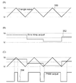
本実施の形態では、開示する発明に係る半導体装置を用いた回路の一例について、図9および図10を参照して説明する。なお、以下では、電力用回路(電力変換用回路など)の一例であるDC−DCコンバータについて説明する。
本実施の形態では、開示する発明の半導体装置を用いて構成されるインバータを備えた太陽光発電システムの一例について、図11を参照して説明する。なお、ここでは、住宅等に設置される太陽光発電システムの構成の一例について示す。
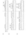
本実施の形態では、半導体装置としてのトランジスタ(特に、薄膜トランジスタ)およびその作製方法の一例について、図12および図13を用いて説明する。なお、以下において説明する半導体装置は、表層部に結晶領域を有する酸化物半導体層を用い、二つの導電層を用いて電流を制御する、新たな構造の半導体装置である。
本実施の形態では、半導体装置としてのトランジスタおよびその作製方法の別の一例について、図14および図15を用いて説明する。
本実施の形態では、いわゆるパワーMOSFETと、薄膜トランジスタとを、同一の基板上に同様の工程で作製する方法の別の一例について、図16および図17を参照して説明する。なお、本実施の形態における半導体装置の作製工程は、多くの部分で先の実施の形態と共通しているから、以下においては、重複する部分の説明は省略する。
本実施の形態では、いわゆるパワーMOSFETと、薄膜トランジスタとを、同一の基板上に同様の工程で作製する方法の別の一例について、図18および図19を参照して説明する。なお、本実施の形態における半導体装置の作製工程は、多くの部分で先の実施の形態と共通しているから、以下においては、重複する部分の説明は省略する。
102 導電層
103 導電層
104 酸化物半導体層
106 結晶領域
108 導電層
109 導電層
110 絶縁層
112 導電層
114 導電層
116 導電層
202 導電層
203 絶縁層
204 酸化物半導体層
206 結晶領域
208 導電層
209 導電層
212 導電層
214 導電層
216 導電層
300 電源
302 リファレンス電圧生成回路
304 リファレンス電流生成回路
306 エラーアンプ
308 PWMバッファ
310 三角波生成回路
312 コイル
314 パワーMOSFET
316 ダイオード
318 コンデンサ
320 抵抗
322 抵抗
350 三角波
352 出力波形
354 パルス信号
400 太陽電池パネル
402 直流開閉器
404 インバータ
406 分電盤
408 交流開閉器
410 電気器具
412 トランス
414 配電線
500 基板
502 導電層
504 レジストマスク
506 導電層
508 絶縁層
510 酸化物半導体層
512 レジストマスク
514 酸化物半導体層
516 導電層
518 レジストマスク
520 レジストマスク
522 導電層
524 導電層
526 絶縁層
528 導電層
530 レジストマスク
532 導電層
550 トランジスタ
600 基板
602 導電層
604 レジストマスク
606 導電層
608 絶縁層
610 導電層
612 レジストマスク
614 レジストマスク
616 導電層
618 導電層
620 酸化物半導体層
622 レジストマスク
624 酸化物半導体層
626 絶縁層
628 導電層
630 レジストマスク
632 導電層
650 トランジスタ
Claims (3)
- 基板上の第1の導電層と、
前記第1の導電層を覆って設けられた第1の絶縁層と、
前記第1の絶縁層上の、チャネル形成領域を有する酸化物半導体層と、
前記酸化物半導体層と接する領域を有する第2の導電層と、
前記酸化物半導体層と接する領域を有する第3の導電層と、
前記酸化物半導体層上、前記第2の導電層上、及び前記第3の導電層上の第2の絶縁層と、
前記第2の絶縁層上の、前記チャネル形成領域と重なる領域を有する第4の導電層と、を有し、
前記第1の導電層は、前記チャネル形成領域と重なる領域を有し、
前記第4の導電層は、前記第2の導電層と重なる領域と、前記第3の導電層と重なる領域と、を有し、
前記酸化物半導体層は、In、Ga、及びZnを含み、
前記酸化物半導体層は、第1の領域と、前記第1の領域上の第2の領域と、を有し、
前記第2の領域は、前記酸化物半導体層表面の垂直方向に沿うようにc軸配向した結晶を含み、
前記第1の領域の結晶性は、前記第2の領域の結晶性よりも低いことを特徴とする半導体装置。 - 基板上の第1の導電層と、
前記第1の導電層を覆う第1の絶縁層と、
前記第1の絶縁層上の、チャネル形成領域を有する酸化物半導体層と、
前記酸化物半導体層と接する領域を有する第2の導電層と、
前記酸化物半導体層と接する領域を有する第3の導電層と、
前記酸化物半導体層上、前記第2の導電層上、及び前記第3の導電層上の第2の絶縁層と、
前記第2の絶縁層上の、前記チャネル形成領域と重なる領域を有する第4の導電層と、を有し、
前記第4の導電層は、前記第2の導電層と重なる領域と、前記第3の導電層と重なる領域と、を有し、
前記第1の導電層は、前記チャネル形成領域と重なる領域と、前記第2の導電層と重なる領域と、前記第3の導電層と重なる領域と、を有し、
前記酸化物半導体層は、In、Ga、及びZnを含み、
前記酸化物半導体層は、第1の領域と、前記第1の領域上の第2の領域と、を有し、
前記第2の領域は、前記酸化物半導体層表面の垂直方向に沿うようにc軸配向した結晶を含み、
前記第1の領域の結晶性は、前記第2の領域の結晶性よりも低いことを特徴とする半導体装置。 - 請求項1又は2において、
前記第4の導電層は、ゲート電極として機能することを特徴とする半導体装置。
Priority Applications (1)
| Application Number | Priority Date | Filing Date | Title |
|---|---|---|---|
| JP2010226397A JP5697396B2 (ja) | 2009-10-09 | 2010-10-06 | 半導体装置 |
Applications Claiming Priority (3)
| Application Number | Priority Date | Filing Date | Title |
|---|---|---|---|
| JP2009235604 | 2009-10-09 | ||
| JP2009235604 | 2009-10-09 | ||
| JP2010226397A JP5697396B2 (ja) | 2009-10-09 | 2010-10-06 | 半導体装置 |
Related Child Applications (1)
| Application Number | Title | Priority Date | Filing Date |
|---|---|---|---|
| JP2015024433A Division JP5893182B2 (ja) | 2009-10-09 | 2015-02-10 | 半導体装置の作製方法 |
Publications (3)
| Publication Number | Publication Date |
|---|---|
| JP2011100992A JP2011100992A (ja) | 2011-05-19 |
| JP2011100992A5 JP2011100992A5 (ja) | 2013-11-21 |
| JP5697396B2 true JP5697396B2 (ja) | 2015-04-08 |
Family
ID=43854111
Family Applications (3)
| Application Number | Title | Priority Date | Filing Date |
|---|---|---|---|
| JP2010226397A Active JP5697396B2 (ja) | 2009-10-09 | 2010-10-06 | 半導体装置 |
| JP2015024433A Active JP5893182B2 (ja) | 2009-10-09 | 2015-02-10 | 半導体装置の作製方法 |
| JP2016032047A Active JP6126713B2 (ja) | 2009-10-09 | 2016-02-23 | 半導体装置 |
Family Applications After (2)
| Application Number | Title | Priority Date | Filing Date |
|---|---|---|---|
| JP2015024433A Active JP5893182B2 (ja) | 2009-10-09 | 2015-02-10 | 半導体装置の作製方法 |
| JP2016032047A Active JP6126713B2 (ja) | 2009-10-09 | 2016-02-23 | 半導体装置 |
Country Status (7)
| Country | Link |
|---|---|
| US (4) | US9006728B2 (ja) |
| EP (1) | EP2486593B1 (ja) |
| JP (3) | JP5697396B2 (ja) |
| KR (3) | KR101820972B1 (ja) |
| CN (1) | CN102576737B (ja) |
| TW (2) | TWI508185B (ja) |
| WO (1) | WO2011043170A1 (ja) |
Families Citing this family (21)
| Publication number | Priority date | Publication date | Assignee | Title |
|---|---|---|---|---|
| KR101820972B1 (ko) | 2009-10-09 | 2018-01-22 | 가부시키가이샤 한도오따이 에네루기 켄큐쇼 | 반도체 장치 및 그 제조 방법 |
| WO2011046015A1 (en) | 2009-10-16 | 2011-04-21 | Semiconductor Energy Laboratory Co., Ltd. | Logic circuit and semiconductor device |
| KR20120096463A (ko) * | 2009-10-21 | 2012-08-30 | 가부시키가이샤 한도오따이 에네루기 켄큐쇼 | 표시 장치 및 표시 장치를 갖는 전자 기기 |
| EP2497115A4 (en) | 2009-11-06 | 2015-09-02 | Semiconductor Energy Lab | SEMICONDUCTOR COMPONENT AND MANUFACTURING METHOD THEREFOR |
| KR101963300B1 (ko) | 2009-12-04 | 2019-03-28 | 가부시키가이샤 한도오따이 에네루기 켄큐쇼 | 표시 장치 |
| CN105023942B (zh) | 2009-12-28 | 2018-11-02 | 株式会社半导体能源研究所 | 制造半导体装置的方法 |
| US8803143B2 (en) * | 2010-10-20 | 2014-08-12 | Semiconductor Energy Laboratory Co., Ltd. | Thin film transistor including buffer layers with high resistivity |
| JP5975635B2 (ja) | 2010-12-28 | 2016-08-23 | 株式会社半導体エネルギー研究所 | 半導体装置 |
| US8709889B2 (en) * | 2011-05-19 | 2014-04-29 | Semiconductor Energy Laboratory Co., Ltd. | Semiconductor memory device and manufacturing method thereof |
| SG10201505586UA (en) * | 2011-06-17 | 2015-08-28 | Semiconductor Energy Lab | Semiconductor device and method for manufacturing the same |
| JP6116149B2 (ja) | 2011-08-24 | 2017-04-19 | 株式会社半導体エネルギー研究所 | 半導体装置 |
| US8698137B2 (en) | 2011-09-14 | 2014-04-15 | Semiconductor Energy Laboratory Co., Ltd. | Semiconductor device |
| US9112037B2 (en) * | 2012-02-09 | 2015-08-18 | Semiconductor Energy Laboratory Co., Ltd. | Semiconductor device |
| US9312390B2 (en) * | 2012-07-05 | 2016-04-12 | Semiconductor Energy Laboratory Co., Ltd. | Remote control system |
| JP2014045175A (ja) | 2012-08-02 | 2014-03-13 | Semiconductor Energy Lab Co Ltd | 半導体装置 |
| US10529740B2 (en) * | 2013-07-25 | 2020-01-07 | Semiconductor Energy Laboratory Co., Ltd. | Semiconductor device including semiconductor layer and conductive layer |
| US20150177311A1 (en) * | 2013-12-19 | 2015-06-25 | Intermolecular, Inc. | Methods and Systems for Evaluating IGZO with Respect to NBIS |
| TWI535034B (zh) * | 2014-01-29 | 2016-05-21 | 友達光電股份有限公司 | 畫素結構及其製作方法 |
| US9722090B2 (en) * | 2014-06-23 | 2017-08-01 | Semiconductor Energy Laboratory Co., Ltd. | Semiconductor device including first gate oxide semiconductor film, and second gate |
| JP6448311B2 (ja) * | 2014-10-30 | 2019-01-09 | 株式会社ジャパンディスプレイ | 半導体装置 |
| US20230187484A1 (en) * | 2021-12-09 | 2023-06-15 | AUO Corporation | Semiconductor device and manufacturing method thereof |
Family Cites Families (204)
| Publication number | Priority date | Publication date | Assignee | Title |
|---|---|---|---|---|
| JPS60198861A (ja) | 1984-03-23 | 1985-10-08 | Fujitsu Ltd | 薄膜トランジスタ |
| JPH0244256B2 (ja) | 1987-01-28 | 1990-10-03 | Kagaku Gijutsucho Mukizaishitsu Kenkyushocho | Ingazn2o5deshimesarerurotsuhoshokeinosojokozoojusurukagobutsuoyobisonoseizoho |
| JPH0244258B2 (ja) | 1987-02-24 | 1990-10-03 | Kagaku Gijutsucho Mukizaishitsu Kenkyushocho | Ingazn3o6deshimesarerurotsuhoshokeinosojokozoojusurukagobutsuoyobisonoseizoho |
| JPH0244260B2 (ja) | 1987-02-24 | 1990-10-03 | Kagaku Gijutsucho Mukizaishitsu Kenkyushocho | Ingazn5o8deshimesarerurotsuhoshokeinosojokozoojusurukagobutsuoyobisonoseizoho |
| JPS63210023A (ja) | 1987-02-24 | 1988-08-31 | Natl Inst For Res In Inorg Mater | InGaZn↓4O↓7で示される六方晶系の層状構造を有する化合物およびその製造法 |
| JPH0244262B2 (ja) | 1987-02-27 | 1990-10-03 | Kagaku Gijutsucho Mukizaishitsu Kenkyushocho | Ingazn6o9deshimesarerurotsuhoshokeinosojokozoojusurukagobutsuoyobisonoseizoho |
| JPH0244263B2 (ja) | 1987-04-22 | 1990-10-03 | Kagaku Gijutsucho Mukizaishitsu Kenkyushocho | Ingazn7o10deshimesarerurotsuhoshokeinosojokozoojusurukagobutsuoyobisonoseizoho |
| JP2653092B2 (ja) * | 1988-03-25 | 1997-09-10 | セイコーエプソン株式会社 | 相補型薄膜トランジスタ及びその製造方法 |
| JP2963529B2 (ja) | 1990-10-29 | 1999-10-18 | シャープ株式会社 | アクティブマトリクス表示装置 |
| JPH05251705A (ja) | 1992-03-04 | 1993-09-28 | Fuji Xerox Co Ltd | 薄膜トランジスタ |
| JPH07176749A (ja) * | 1993-12-20 | 1995-07-14 | Sharp Corp | 薄膜トランジスタ |
| JP3947575B2 (ja) | 1994-06-10 | 2007-07-25 | Hoya株式会社 | 導電性酸化物およびそれを用いた電極 |
| JP3479375B2 (ja) | 1995-03-27 | 2003-12-15 | 科学技術振興事業団 | 亜酸化銅等の金属酸化物半導体による薄膜トランジスタとpn接合を形成した金属酸化物半導体装置およびそれらの製造方法 |
| DE69635107D1 (de) * | 1995-08-03 | 2005-09-29 | Koninkl Philips Electronics Nv | Halbleiteranordnung mit einem transparenten schaltungselement |
| JPH0996836A (ja) | 1995-09-29 | 1997-04-08 | Toshiba Corp | 液晶表示装置 |
| JP3625598B2 (ja) * | 1995-12-30 | 2005-03-02 | 三星電子株式会社 | 液晶表示装置の製造方法 |
| US6211928B1 (en) * | 1996-03-26 | 2001-04-03 | Lg Electronics Inc. | Liquid crystal display and method for manufacturing the same |
| DE19712233C2 (de) | 1996-03-26 | 2003-12-11 | Lg Philips Lcd Co | Flüssigkristallanzeige und Herstellungsverfahren dafür |
| US6001539A (en) | 1996-04-08 | 1999-12-14 | Lg Electronics, Inc. | Method for manufacturing liquid crystal display |
| US6188452B1 (en) * | 1996-07-09 | 2001-02-13 | Lg Electronics, Inc | Active matrix liquid crystal display and method of manufacturing same |
| JP4170454B2 (ja) | 1998-07-24 | 2008-10-22 | Hoya株式会社 | 透明導電性酸化物薄膜を有する物品及びその製造方法 |
| JP2000150861A (ja) | 1998-11-16 | 2000-05-30 | Tdk Corp | 酸化物薄膜 |
| JP3276930B2 (ja) * | 1998-11-17 | 2002-04-22 | 科学技術振興事業団 | トランジスタ及び半導体装置 |
| TW460731B (en) | 1999-09-03 | 2001-10-21 | Ind Tech Res Inst | Electrode structure and production method of wide viewing angle LCD |
| JP4089858B2 (ja) | 2000-09-01 | 2008-05-28 | 国立大学法人東北大学 | 半導体デバイス |
| KR20020038482A (ko) * | 2000-11-15 | 2002-05-23 | 모리시타 요이찌 | 박막 트랜지스터 어레이, 그 제조방법 및 그것을 이용한표시패널 |
| JP3997731B2 (ja) | 2001-03-19 | 2007-10-24 | 富士ゼロックス株式会社 | 基材上に結晶性半導体薄膜を形成する方法 |
| JP2002289859A (ja) | 2001-03-23 | 2002-10-04 | Minolta Co Ltd | 薄膜トランジスタ |
| JP3716755B2 (ja) | 2001-04-05 | 2005-11-16 | 株式会社日立製作所 | アクティブマトリクス型表示装置 |
| JP3694737B2 (ja) | 2001-07-27 | 2005-09-14 | 独立行政法人物質・材料研究機構 | 酸化亜鉛基ホモロガス化合物薄膜の製造法 |
| JP4090716B2 (ja) | 2001-09-10 | 2008-05-28 | 雅司 川崎 | 薄膜トランジスタおよびマトリクス表示装置 |
| JP3925839B2 (ja) | 2001-09-10 | 2007-06-06 | シャープ株式会社 | 半導体記憶装置およびその試験方法 |
| WO2003040441A1 (fr) * | 2001-11-05 | 2003-05-15 | Japan Science And Technology Agency | Film mince monocristallin homologue a super-reseau naturel, procede de preparation et dispositif dans lequel est utilise ledit film mince monocristallin |
| JP4164562B2 (ja) | 2002-09-11 | 2008-10-15 | 独立行政法人科学技術振興機構 | ホモロガス薄膜を活性層として用いる透明薄膜電界効果型トランジスタ |
| JP4083486B2 (ja) * | 2002-02-21 | 2008-04-30 | 独立行政法人科学技術振興機構 | LnCuO(S,Se,Te)単結晶薄膜の製造方法 |
| JP4515035B2 (ja) | 2002-03-14 | 2010-07-28 | 株式会社半導体エネルギー研究所 | 表示装置及びその作製方法 |
| US6885146B2 (en) | 2002-03-14 | 2005-04-26 | Semiconductor Energy Laboratory Co., Ltd. | Display device comprising substrates, contrast medium and barrier layers between contrast medium and each of substrates |
| US7049190B2 (en) * | 2002-03-15 | 2006-05-23 | Sanyo Electric Co., Ltd. | Method for forming ZnO film, method for forming ZnO semiconductor layer, method for fabricating semiconductor device, and semiconductor device |
| JP3933591B2 (ja) | 2002-03-26 | 2007-06-20 | 淳二 城戸 | 有機エレクトロルミネッセント素子 |
| US7339187B2 (en) * | 2002-05-21 | 2008-03-04 | State Of Oregon Acting By And Through The Oregon State Board Of Higher Education On Behalf Of Oregon State University | Transistor structures |
| JP2004022625A (ja) * | 2002-06-13 | 2004-01-22 | Murata Mfg Co Ltd | 半導体デバイス及び該半導体デバイスの製造方法 |
| US7105868B2 (en) | 2002-06-24 | 2006-09-12 | Cermet, Inc. | High-electron mobility transistor with zinc oxide |
| US7067843B2 (en) | 2002-10-11 | 2006-06-27 | E. I. Du Pont De Nemours And Company | Transparent oxide semiconductor thin film transistors |
| CN1723741B (zh) | 2002-12-12 | 2012-09-05 | 株式会社半导体能源研究所 | 发光装置、制造装置、成膜方法及清洁方法 |
| JP4166105B2 (ja) | 2003-03-06 | 2008-10-15 | シャープ株式会社 | 半導体装置およびその製造方法 |
| JP2004273732A (ja) | 2003-03-07 | 2004-09-30 | Sharp Corp | アクティブマトリクス基板およびその製造方法 |
| JP4108633B2 (ja) | 2003-06-20 | 2008-06-25 | シャープ株式会社 | 薄膜トランジスタおよびその製造方法ならびに電子デバイス |
| US20050031799A1 (en) | 2003-06-25 | 2005-02-10 | Fuji Photo Film Co., Ltd. | Process for preparing radiation image storage panel |
| US7262463B2 (en) * | 2003-07-25 | 2007-08-28 | Hewlett-Packard Development Company, L.P. | Transistor including a deposited channel region having a doped portion |
| EP1737044B1 (en) | 2004-03-12 | 2014-12-10 | Japan Science and Technology Agency | Amorphous oxide and thin film transistor |
| US7282782B2 (en) | 2004-03-12 | 2007-10-16 | Hewlett-Packard Development Company, L.P. | Combined binary oxide semiconductor device |
| US7297977B2 (en) * | 2004-03-12 | 2007-11-20 | Hewlett-Packard Development Company, L.P. | Semiconductor device |
| US7145174B2 (en) | 2004-03-12 | 2006-12-05 | Hewlett-Packard Development Company, Lp. | Semiconductor device |
| US7211825B2 (en) * | 2004-06-14 | 2007-05-01 | Yi-Chi Shih | Indium oxide-based thin film transistors and circuits |
| JP2006100760A (ja) * | 2004-09-02 | 2006-04-13 | Casio Comput Co Ltd | 薄膜トランジスタおよびその製造方法 |
| US7285501B2 (en) * | 2004-09-17 | 2007-10-23 | Hewlett-Packard Development Company, L.P. | Method of forming a solution processed device |
| US7298084B2 (en) * | 2004-11-02 | 2007-11-20 | 3M Innovative Properties Company | Methods and displays utilizing integrated zinc oxide row and column drivers in conjunction with organic light emitting diodes |
| KR101074389B1 (ko) * | 2004-11-05 | 2011-10-17 | 엘지디스플레이 주식회사 | 박막 식각 방법 및 이를 이용한 액정표시장치의 제조방법 |
| RU2358354C2 (ru) * | 2004-11-10 | 2009-06-10 | Кэнон Кабусики Кайся | Светоизлучающее устройство |
| KR100669752B1 (ko) * | 2004-11-10 | 2007-01-16 | 삼성에스디아이 주식회사 | 유기 박막 트랜지스터, 이의 제조 방법 및 이를 구비한평판표시장치 |
| CN102945857B (zh) * | 2004-11-10 | 2015-06-03 | 佳能株式会社 | 无定形氧化物和场效应晶体管 |
| WO2006051995A1 (en) * | 2004-11-10 | 2006-05-18 | Canon Kabushiki Kaisha | Field effect transistor employing an amorphous oxide |
| US7791072B2 (en) * | 2004-11-10 | 2010-09-07 | Canon Kabushiki Kaisha | Display |
| US7453065B2 (en) * | 2004-11-10 | 2008-11-18 | Canon Kabushiki Kaisha | Sensor and image pickup device |
| US7829444B2 (en) * | 2004-11-10 | 2010-11-09 | Canon Kabushiki Kaisha | Field effect transistor manufacturing method |
| US7863611B2 (en) * | 2004-11-10 | 2011-01-04 | Canon Kabushiki Kaisha | Integrated circuits utilizing amorphous oxides |
| EP1670079B1 (en) * | 2004-12-08 | 2010-12-01 | Samsung Mobile Display Co., Ltd. | Method of forming a conductive pattern of a thin film transistor |
| KR100662790B1 (ko) * | 2004-12-28 | 2007-01-02 | 엘지.필립스 엘시디 주식회사 | 액정표시장치 및 그 제조방법 |
| US7579224B2 (en) * | 2005-01-21 | 2009-08-25 | Semiconductor Energy Laboratory Co., Ltd. | Method for manufacturing a thin film semiconductor device |
| TWI505473B (zh) | 2005-01-28 | 2015-10-21 | 半導體能源研究所股份有限公司 | 半導體裝置,電子裝置,和半導體裝置的製造方法 |
| TWI569441B (zh) | 2005-01-28 | 2017-02-01 | 半導體能源研究所股份有限公司 | 半導體裝置,電子裝置,和半導體裝置的製造方法 |
| JP4761981B2 (ja) * | 2005-01-28 | 2011-08-31 | 株式会社半導体エネルギー研究所 | 半導体装置の作製方法 |
| US7858451B2 (en) * | 2005-02-03 | 2010-12-28 | Semiconductor Energy Laboratory Co., Ltd. | Electronic device, semiconductor device and manufacturing method thereof |
| US7948171B2 (en) * | 2005-02-18 | 2011-05-24 | Semiconductor Energy Laboratory Co., Ltd. | Light emitting device |
| US20060197092A1 (en) | 2005-03-03 | 2006-09-07 | Randy Hoffman | System and method for forming conductive material on a substrate |
| US8681077B2 (en) | 2005-03-18 | 2014-03-25 | Semiconductor Energy Laboratory Co., Ltd. | Semiconductor device, and display device, driving method and electronic apparatus thereof |
| US7544967B2 (en) | 2005-03-28 | 2009-06-09 | Massachusetts Institute Of Technology | Low voltage flexible organic/transparent transistor for selective gas sensing, photodetecting and CMOS device applications |
| US7645478B2 (en) | 2005-03-31 | 2010-01-12 | 3M Innovative Properties Company | Methods of making displays |
| US8300031B2 (en) | 2005-04-20 | 2012-10-30 | Semiconductor Energy Laboratory Co., Ltd. | Semiconductor device comprising transistor having gate and drain connected through a current-voltage conversion element |
| JP2006344849A (ja) | 2005-06-10 | 2006-12-21 | Casio Comput Co Ltd | 薄膜トランジスタ |
| US7691666B2 (en) | 2005-06-16 | 2010-04-06 | Eastman Kodak Company | Methods of making thin film transistors comprising zinc-oxide-based semiconductor materials and transistors made thereby |
| US7402506B2 (en) | 2005-06-16 | 2008-07-22 | Eastman Kodak Company | Methods of making thin film transistors comprising zinc-oxide-based semiconductor materials and transistors made thereby |
| US7507618B2 (en) | 2005-06-27 | 2009-03-24 | 3M Innovative Properties Company | Method for making electronic devices using metal oxide nanoparticles |
| JP5036241B2 (ja) * | 2005-07-27 | 2012-09-26 | 株式会社半導体エネルギー研究所 | 半導体装置の作製方法 |
| US7655566B2 (en) * | 2005-07-27 | 2010-02-02 | Semiconductor Energy Laboratory Co., Ltd. | Method for manufacturing semiconductor device |
| KR100711890B1 (ko) * | 2005-07-28 | 2007-04-25 | 삼성에스디아이 주식회사 | 유기 발광표시장치 및 그의 제조방법 |
| JP2007059128A (ja) * | 2005-08-23 | 2007-03-08 | Canon Inc | 有機el表示装置およびその製造方法 |
| JP2007073705A (ja) * | 2005-09-06 | 2007-03-22 | Canon Inc | 酸化物半導体チャネル薄膜トランジスタおよびその製造方法 |
| JP4850457B2 (ja) | 2005-09-06 | 2012-01-11 | キヤノン株式会社 | 薄膜トランジスタ及び薄膜ダイオード |
| JP5116225B2 (ja) * | 2005-09-06 | 2013-01-09 | キヤノン株式会社 | 酸化物半導体デバイスの製造方法 |
| JP4280736B2 (ja) * | 2005-09-06 | 2009-06-17 | キヤノン株式会社 | 半導体素子 |
| JP4560502B2 (ja) * | 2005-09-06 | 2010-10-13 | キヤノン株式会社 | 電界効果型トランジスタ |
| JP5064747B2 (ja) * | 2005-09-29 | 2012-10-31 | 株式会社半導体エネルギー研究所 | 半導体装置、電気泳動表示装置、表示モジュール、電子機器、及び半導体装置の作製方法 |
| EP1995787A3 (en) * | 2005-09-29 | 2012-01-18 | Semiconductor Energy Laboratory Co, Ltd. | Semiconductor device having oxide semiconductor layer and manufacturing method therof |
| JP5078246B2 (ja) | 2005-09-29 | 2012-11-21 | 株式会社半導体エネルギー研究所 | 半導体装置、及び半導体装置の作製方法 |
| JP5037808B2 (ja) * | 2005-10-20 | 2012-10-03 | キヤノン株式会社 | アモルファス酸化物を用いた電界効果型トランジスタ、及び該トランジスタを用いた表示装置 |
| JP4560505B2 (ja) * | 2005-11-08 | 2010-10-13 | キヤノン株式会社 | 電界効果型トランジスタ |
| KR101050767B1 (ko) * | 2005-11-15 | 2011-07-20 | 가부시키가이샤 한도오따이 에네루기 켄큐쇼 | 반도체장치 제조방법 |
| JP5376750B2 (ja) | 2005-11-18 | 2013-12-25 | 出光興産株式会社 | 半導体薄膜、及びその製造方法、並びに薄膜トランジスタ、アクティブマトリックス駆動表示パネル |
| US7998372B2 (en) | 2005-11-18 | 2011-08-16 | Idemitsu Kosan Co., Ltd. | Semiconductor thin film, method for manufacturing the same, thin film transistor, and active-matrix-driven display panel |
| TWI292281B (en) | 2005-12-29 | 2008-01-01 | Ind Tech Res Inst | Pixel structure of active organic light emitting diode and method of fabricating the same |
| US7867636B2 (en) * | 2006-01-11 | 2011-01-11 | Murata Manufacturing Co., Ltd. | Transparent conductive film and method for manufacturing the same |
| JP4977478B2 (ja) | 2006-01-21 | 2012-07-18 | 三星電子株式会社 | ZnOフィルム及びこれを用いたTFTの製造方法 |
| US7576394B2 (en) | 2006-02-02 | 2009-08-18 | Kochi Industrial Promotion Center | Thin film transistor including low resistance conductive thin films and manufacturing method thereof |
| JP5015473B2 (ja) | 2006-02-15 | 2012-08-29 | 財団法人高知県産業振興センター | 薄膜トランジスタアレイ及びその製法 |
| US7977169B2 (en) | 2006-02-15 | 2011-07-12 | Kochi Industrial Promotion Center | Semiconductor device including active layer made of zinc oxide with controlled orientations and manufacturing method thereof |
| JP2007250982A (ja) * | 2006-03-17 | 2007-09-27 | Canon Inc | 酸化物半導体を用いた薄膜トランジスタ及び表示装置 |
| KR20070101595A (ko) | 2006-04-11 | 2007-10-17 | 삼성전자주식회사 | ZnO TFT |
| JP5060738B2 (ja) * | 2006-04-28 | 2012-10-31 | 株式会社ジャパンディスプレイイースト | 画像表示装置 |
| US20070252928A1 (en) | 2006-04-28 | 2007-11-01 | Toppan Printing Co., Ltd. | Structure, transmission type liquid crystal display, reflection type display and manufacturing method thereof |
| CN101356652B (zh) | 2006-06-02 | 2012-04-18 | 日本财团法人高知县产业振兴中心 | 包括由氧化锌构成的氧化物半导体薄膜层的半导体器件及其制造方法 |
| US20070287221A1 (en) * | 2006-06-12 | 2007-12-13 | Xerox Corporation | Fabrication process for crystalline zinc oxide semiconductor layer |
| JP5028033B2 (ja) | 2006-06-13 | 2012-09-19 | キヤノン株式会社 | 酸化物半導体膜のドライエッチング方法 |
| KR101183361B1 (ko) * | 2006-06-29 | 2012-09-14 | 엘지디스플레이 주식회사 | 액정 표시 장치용 어레이 기판 및 그 제조 방법 |
| JP5328083B2 (ja) * | 2006-08-01 | 2013-10-30 | キヤノン株式会社 | 酸化物のエッチング方法 |
| JP4609797B2 (ja) * | 2006-08-09 | 2011-01-12 | Nec液晶テクノロジー株式会社 | 薄膜デバイス及びその製造方法 |
| JP4999400B2 (ja) * | 2006-08-09 | 2012-08-15 | キヤノン株式会社 | 酸化物半導体膜のドライエッチング方法 |
| JP4919738B2 (ja) * | 2006-08-31 | 2012-04-18 | 株式会社半導体エネルギー研究所 | 半導体装置の作製方法 |
| JP5128792B2 (ja) * | 2006-08-31 | 2013-01-23 | 財団法人高知県産業振興センター | 薄膜トランジスタの製法 |
| JP4332545B2 (ja) | 2006-09-15 | 2009-09-16 | キヤノン株式会社 | 電界効果型トランジスタ及びその製造方法 |
| JP4274219B2 (ja) * | 2006-09-27 | 2009-06-03 | セイコーエプソン株式会社 | 電子デバイス、有機エレクトロルミネッセンス装置、有機薄膜半導体装置 |
| JP5164357B2 (ja) * | 2006-09-27 | 2013-03-21 | キヤノン株式会社 | 半導体装置及び半導体装置の製造方法 |
| US7622371B2 (en) * | 2006-10-10 | 2009-11-24 | Hewlett-Packard Development Company, L.P. | Fused nanocrystal thin film semiconductor and method |
| US7767595B2 (en) * | 2006-10-26 | 2010-08-03 | Semiconductor Energy Laboratory Co., Ltd. | Manufacturing method of semiconductor device |
| JP5227563B2 (ja) | 2006-10-26 | 2013-07-03 | 株式会社半導体エネルギー研究所 | 半導体装置の作製方法 |
| US7772021B2 (en) * | 2006-11-29 | 2010-08-10 | Samsung Electronics Co., Ltd. | Flat panel displays comprising a thin-film transistor having a semiconductive oxide in its channel and methods of fabricating the same for use in flat panel displays |
| JP2008140684A (ja) * | 2006-12-04 | 2008-06-19 | Toppan Printing Co Ltd | カラーelディスプレイおよびその製造方法 |
| KR101303578B1 (ko) | 2007-01-05 | 2013-09-09 | 삼성전자주식회사 | 박막 식각 방법 |
| US8207063B2 (en) | 2007-01-26 | 2012-06-26 | Eastman Kodak Company | Process for atomic layer deposition |
| US8436349B2 (en) | 2007-02-20 | 2013-05-07 | Canon Kabushiki Kaisha | Thin-film transistor fabrication process and display device |
| JP4910779B2 (ja) * | 2007-03-02 | 2012-04-04 | 凸版印刷株式会社 | 有機elディスプレイおよびその製造方法 |
| KR100851215B1 (ko) | 2007-03-14 | 2008-08-07 | 삼성에스디아이 주식회사 | 박막 트랜지스터 및 이를 이용한 유기 전계 발광표시장치 |
| JP5244331B2 (ja) * | 2007-03-26 | 2013-07-24 | 出光興産株式会社 | 非晶質酸化物半導体薄膜、その製造方法、薄膜トランジスタの製造方法、電界効果型トランジスタ、発光装置、表示装置及びスパッタリングターゲット |
| JP5465825B2 (ja) | 2007-03-26 | 2014-04-09 | 出光興産株式会社 | 半導体装置、半導体装置の製造方法及び表示装置 |
| JP2008276212A (ja) * | 2007-04-05 | 2008-11-13 | Fujifilm Corp | 有機電界発光表示装置 |
| WO2008126879A1 (en) * | 2007-04-09 | 2008-10-23 | Canon Kabushiki Kaisha | Light-emitting apparatus and production method thereof |
| JP5197058B2 (ja) * | 2007-04-09 | 2013-05-15 | キヤノン株式会社 | 発光装置とその作製方法 |
| US7795613B2 (en) | 2007-04-17 | 2010-09-14 | Toppan Printing Co., Ltd. | Structure with transistor |
| KR101325053B1 (ko) | 2007-04-18 | 2013-11-05 | 삼성디스플레이 주식회사 | 박막 트랜지스터 기판 및 이의 제조 방법 |
| KR20080094300A (ko) | 2007-04-19 | 2008-10-23 | 삼성전자주식회사 | 박막 트랜지스터 및 그 제조 방법과 박막 트랜지스터를포함하는 평판 디스플레이 |
| KR101334181B1 (ko) * | 2007-04-20 | 2013-11-28 | 삼성전자주식회사 | 선택적으로 결정화된 채널층을 갖는 박막 트랜지스터 및 그제조 방법 |
| US8274078B2 (en) * | 2007-04-25 | 2012-09-25 | Canon Kabushiki Kaisha | Metal oxynitride semiconductor containing zinc |
| KR101345376B1 (ko) | 2007-05-29 | 2013-12-24 | 삼성전자주식회사 | ZnO 계 박막 트랜지스터 및 그 제조방법 |
| JP5241143B2 (ja) | 2007-05-30 | 2013-07-17 | キヤノン株式会社 | 電界効果型トランジスタ |
| US7935964B2 (en) * | 2007-06-19 | 2011-05-03 | Samsung Electronics Co., Ltd. | Oxide semiconductors and thin film transistors comprising the same |
| US8354674B2 (en) * | 2007-06-29 | 2013-01-15 | Semiconductor Energy Laboratory Co., Ltd. | Semiconductor device wherein a property of a first semiconductor layer is different from a property of a second semiconductor layer |
| KR20090002841A (ko) * | 2007-07-04 | 2009-01-09 | 삼성전자주식회사 | 산화물 반도체, 이를 포함하는 박막 트랜지스터 및 그 제조방법 |
| KR100889688B1 (ko) | 2007-07-16 | 2009-03-19 | 삼성모바일디스플레이주식회사 | 반도체 활성층 제조 방법, 그를 이용한 박막 트랜지스터의제조 방법 및 반도체 활성층을 구비하는 박막 트랜지스터 |
| JP4759598B2 (ja) | 2007-09-28 | 2011-08-31 | キヤノン株式会社 | 薄膜トランジスタ、その製造方法及びそれを用いた表示装置 |
| JP2009099847A (ja) * | 2007-10-18 | 2009-05-07 | Canon Inc | 薄膜トランジスタとその製造方法及び表示装置 |
| TW200921226A (en) * | 2007-11-06 | 2009-05-16 | Wintek Corp | Panel structure and manufacture method thereof |
| KR101594335B1 (ko) * | 2007-12-03 | 2016-02-16 | 가부시키가이샤 한도오따이 에네루기 켄큐쇼 | 반도체 장치 및 그 제조 방법 |
| JP5215158B2 (ja) | 2007-12-17 | 2013-06-19 | 富士フイルム株式会社 | 無機結晶性配向膜及びその製造方法、半導体デバイス |
| JP5264197B2 (ja) | 2008-01-23 | 2013-08-14 | キヤノン株式会社 | 薄膜トランジスタ |
| US8586979B2 (en) | 2008-02-01 | 2013-11-19 | Samsung Electronics Co., Ltd. | Oxide semiconductor transistor and method of manufacturing the same |
| KR100870838B1 (ko) | 2008-03-04 | 2008-11-28 | 한국철강 주식회사 | 투명전극이 코팅된 기판의 수분 제거방법 |
| JP5467728B2 (ja) * | 2008-03-14 | 2014-04-09 | 富士フイルム株式会社 | 薄膜電界効果型トランジスタおよびその製造方法 |
| KR101461127B1 (ko) * | 2008-05-13 | 2014-11-14 | 삼성디스플레이 주식회사 | 반도체 장치 및 이의 제조 방법 |
| KR101497425B1 (ko) * | 2008-08-28 | 2015-03-03 | 삼성디스플레이 주식회사 | 액정 표시 장치 및 그 제조 방법 |
| US9082857B2 (en) * | 2008-09-01 | 2015-07-14 | Semiconductor Energy Laboratory Co., Ltd. | Semiconductor device comprising an oxide semiconductor layer |
| KR101772377B1 (ko) * | 2008-09-12 | 2017-08-29 | 가부시키가이샤 한도오따이 에네루기 켄큐쇼 | 표시 장치 |
| KR20110056542A (ko) * | 2008-09-12 | 2011-05-30 | 가부시키가이샤 한도오따이 에네루기 켄큐쇼 | 표시 장치 |
| JP4623179B2 (ja) * | 2008-09-18 | 2011-02-02 | ソニー株式会社 | 薄膜トランジスタおよびその製造方法 |
| KR101563527B1 (ko) * | 2008-09-19 | 2015-10-27 | 가부시키가이샤 한도오따이 에네루기 켄큐쇼 | 반도체장치 |
| KR101999970B1 (ko) | 2008-09-19 | 2019-07-15 | 가부시키가이샤 한도오따이 에네루기 켄큐쇼 | 반도체 장치 |
| EP2172977A1 (en) * | 2008-10-03 | 2010-04-07 | Semiconductor Energy Laboratory Co., Ltd. | Display device |
| KR101961632B1 (ko) | 2008-10-03 | 2019-03-25 | 가부시키가이샤 한도오따이 에네루기 켄큐쇼 | 표시장치 |
| JP5451280B2 (ja) * | 2008-10-09 | 2014-03-26 | キヤノン株式会社 | ウルツ鉱型結晶成長用基板およびその製造方法ならびに半導体装置 |
| JP5361651B2 (ja) * | 2008-10-22 | 2013-12-04 | 株式会社半導体エネルギー研究所 | 半導体装置の作製方法 |
| JP5616012B2 (ja) * | 2008-10-24 | 2014-10-29 | 株式会社半導体エネルギー研究所 | 半導体装置の作製方法 |
| KR102251817B1 (ko) * | 2008-10-24 | 2021-05-12 | 가부시키가이샤 한도오따이 에네루기 켄큐쇼 | 반도체 장치 및 그 제조 방법 |
| KR101667909B1 (ko) | 2008-10-24 | 2016-10-28 | 가부시키가이샤 한도오따이 에네루기 켄큐쇼 | 반도체장치의 제조방법 |
| EP2180518B1 (en) | 2008-10-24 | 2018-04-25 | Semiconductor Energy Laboratory Co, Ltd. | Method for manufacturing semiconductor device |
| US8741702B2 (en) * | 2008-10-24 | 2014-06-03 | Semiconductor Energy Laboratory Co., Ltd. | Method for manufacturing semiconductor device |
| WO2010047288A1 (en) * | 2008-10-24 | 2010-04-29 | Semiconductor Energy Laboratory Co., Ltd. | Method for manufacturing semiconductordevice |
| KR20110084523A (ko) * | 2008-11-07 | 2011-07-25 | 가부시키가이샤 한도오따이 에네루기 켄큐쇼 | 반도체 장치 |
| KR101671544B1 (ko) | 2008-11-21 | 2016-11-01 | 가부시키가이샤 한도오따이 에네루기 켄큐쇼 | 반도체 장치, 표시 장치 및 전자 기기 |
| JP5564331B2 (ja) | 2009-05-29 | 2014-07-30 | 株式会社半導体エネルギー研究所 | 半導体装置の作製方法 |
| JP2011071476A (ja) * | 2009-08-25 | 2011-04-07 | Canon Inc | 薄膜トランジスタ、薄膜トランジスタを用いた表示装置及び薄膜トランジスタの製造方法 |
| WO2011027661A1 (en) | 2009-09-04 | 2011-03-10 | Semiconductor Energy Laboratory Co., Ltd. | Light-emitting device and method for manufacturing the same |
| KR101519893B1 (ko) * | 2009-09-16 | 2015-05-14 | 가부시키가이샤 한도오따이 에네루기 켄큐쇼 | 트랜지스터 |
| KR20230165355A (ko) * | 2009-09-16 | 2023-12-05 | 가부시키가이샤 한도오따이 에네루기 켄큐쇼 | 표시 장치 |
| KR101608923B1 (ko) * | 2009-09-24 | 2016-04-04 | 가부시키가이샤 한도오따이 에네루기 켄큐쇼 | 산화물 반도체막 및 반도체 장치 |
| KR101623619B1 (ko) * | 2009-10-08 | 2016-05-23 | 가부시키가이샤 한도오따이 에네루기 켄큐쇼 | 산화물 반도체층 및 반도체 장치 |
| KR102596694B1 (ko) * | 2009-10-08 | 2023-11-01 | 가부시키가이샤 한도오따이 에네루기 켄큐쇼 | 표시 장치 |
| KR101820972B1 (ko) * | 2009-10-09 | 2018-01-22 | 가부시키가이샤 한도오따이 에네루기 켄큐쇼 | 반도체 장치 및 그 제조 방법 |
| KR101832698B1 (ko) | 2009-10-14 | 2018-02-28 | 가부시키가이샤 한도오따이 에네루기 켄큐쇼 | 반도체 장치 및 그 제작 방법 |
| WO2011052383A1 (en) | 2009-10-30 | 2011-05-05 | Semiconductor Energy Laboratory Co., Ltd. | Logic circuit and semiconductor device |
| EP2497115A4 (en) * | 2009-11-06 | 2015-09-02 | Semiconductor Energy Lab | SEMICONDUCTOR COMPONENT AND MANUFACTURING METHOD THEREFOR |
| KR102484475B1 (ko) * | 2009-11-06 | 2023-01-04 | 가부시키가이샤 한도오따이 에네루기 켄큐쇼 | 반도체 장치 및 그 제작 방법 |
| KR20190100462A (ko) * | 2009-11-28 | 2019-08-28 | 가부시키가이샤 한도오따이 에네루기 켄큐쇼 | 반도체 장치 및 그 제조 방법 |
| KR101803553B1 (ko) * | 2009-11-28 | 2017-11-30 | 가부시키가이샤 한도오따이 에네루기 켄큐쇼 | 반도체 장치 및 그 제작 방법 |
| WO2011065210A1 (en) * | 2009-11-28 | 2011-06-03 | Semiconductor Energy Laboratory Co., Ltd. | Stacked oxide material, semiconductor device, and method for manufacturing the semiconductor device |
| CN105206514B (zh) * | 2009-11-28 | 2018-04-10 | 株式会社半导体能源研究所 | 层叠的氧化物材料、半导体器件、以及用于制造该半导体器件的方法 |
| KR102719739B1 (ko) | 2009-12-04 | 2024-10-21 | 가부시키가이샤 한도오따이 에네루기 켄큐쇼 | 반도체 장치 |
| KR102450889B1 (ko) | 2009-12-04 | 2022-10-06 | 가부시키가이샤 한도오따이 에네루기 켄큐쇼 | 반도체 장치 |
| KR101963300B1 (ko) | 2009-12-04 | 2019-03-28 | 가부시키가이샤 한도오따이 에네루기 켄큐쇼 | 표시 장치 |
| KR101470303B1 (ko) | 2009-12-08 | 2014-12-09 | 가부시키가이샤 한도오따이 에네루기 켄큐쇼 | 반도체 장치 |
| JP5731369B2 (ja) | 2010-12-28 | 2015-06-10 | 株式会社半導体エネルギー研究所 | 半導体装置の作製方法 |
| JP5975635B2 (ja) | 2010-12-28 | 2016-08-23 | 株式会社半導体エネルギー研究所 | 半導体装置 |
| TWI581431B (zh) * | 2012-01-26 | 2017-05-01 | 半導體能源研究所股份有限公司 | 半導體裝置及半導體裝置的製造方法 |
| US9362417B2 (en) * | 2012-02-03 | 2016-06-07 | Semiconductor Energy Laboratory Co., Ltd. | Semiconductor device |
| US9859114B2 (en) * | 2012-02-08 | 2018-01-02 | Semiconductor Energy Laboratory Co., Ltd. | Oxide semiconductor device with an oxygen-controlling insulating layer |
| US20130221345A1 (en) * | 2012-02-28 | 2013-08-29 | Semiconductor Energy Laboratory Co., Ltd. | Semiconductor device and method for manufacturing the same |
-
2010
- 2010-09-09 KR KR1020127009196A patent/KR101820972B1/ko not_active Expired - Fee Related
- 2010-09-09 CN CN201080046496.6A patent/CN102576737B/zh active Active
- 2010-09-09 KR KR1020127018502A patent/KR101396096B1/ko not_active Expired - Fee Related
- 2010-09-09 WO PCT/JP2010/065990 patent/WO2011043170A1/en not_active Ceased
- 2010-09-09 EP EP10821841.3A patent/EP2486593B1/en not_active Not-in-force
- 2010-09-09 KR KR1020187001272A patent/KR101959693B1/ko not_active Expired - Fee Related
- 2010-09-27 TW TW099132603A patent/TWI508185B/zh not_active IP Right Cessation
- 2010-09-27 TW TW104127323A patent/TWI595648B/zh active
- 2010-09-30 US US12/894,911 patent/US9006728B2/en active Active
- 2010-10-06 JP JP2010226397A patent/JP5697396B2/ja active Active
-
2014
- 2014-02-18 US US14/182,726 patent/US8999751B2/en active Active
-
2015
- 2015-02-10 JP JP2015024433A patent/JP5893182B2/ja active Active
- 2015-04-02 US US14/677,180 patent/US9349791B2/en active Active
-
2016
- 2016-02-23 JP JP2016032047A patent/JP6126713B2/ja active Active
- 2016-05-12 US US15/153,119 patent/US9941413B2/en not_active Expired - Fee Related
Also Published As
| Publication number | Publication date |
|---|---|
| KR20180009385A (ko) | 2018-01-26 |
| JP2016122857A (ja) | 2016-07-07 |
| JP6126713B2 (ja) | 2017-05-10 |
| TW201130057A (en) | 2011-09-01 |
| KR101959693B1 (ko) | 2019-03-18 |
| WO2011043170A1 (en) | 2011-04-14 |
| US20140162402A1 (en) | 2014-06-12 |
| JP2015122531A (ja) | 2015-07-02 |
| TW201601309A (zh) | 2016-01-01 |
| KR20120093871A (ko) | 2012-08-23 |
| CN102576737B (zh) | 2015-10-21 |
| US8999751B2 (en) | 2015-04-07 |
| TWI595648B (zh) | 2017-08-11 |
| US20160260839A1 (en) | 2016-09-08 |
| CN102576737A (zh) | 2012-07-11 |
| EP2486593A4 (en) | 2014-04-23 |
| JP5893182B2 (ja) | 2016-03-23 |
| JP2011100992A (ja) | 2011-05-19 |
| EP2486593A1 (en) | 2012-08-15 |
| US9941413B2 (en) | 2018-04-10 |
| KR101396096B1 (ko) | 2014-05-15 |
| US20110084263A1 (en) | 2011-04-14 |
| TWI508185B (zh) | 2015-11-11 |
| KR101820972B1 (ko) | 2018-01-22 |
| US9006728B2 (en) | 2015-04-14 |
| US20150279929A1 (en) | 2015-10-01 |
| US9349791B2 (en) | 2016-05-24 |
| KR20120099491A (ko) | 2012-09-10 |
| EP2486593B1 (en) | 2017-02-01 |
Similar Documents
| Publication | Publication Date | Title |
|---|---|---|
| JP5697396B2 (ja) | 半導体装置 | |
| JP5679749B2 (ja) | 半導体装置 | |
| JP7713079B2 (ja) | 表示装置 |
Legal Events
| Date | Code | Title | Description |
|---|---|---|---|
| A521 | Request for written amendment filed |
Free format text: JAPANESE INTERMEDIATE CODE: A523 Effective date: 20131004 |
|
| A621 | Written request for application examination |
Free format text: JAPANESE INTERMEDIATE CODE: A621 Effective date: 20131004 |
|
| A977 | Report on retrieval |
Free format text: JAPANESE INTERMEDIATE CODE: A971007 Effective date: 20140828 |
|
| A131 | Notification of reasons for refusal |
Free format text: JAPANESE INTERMEDIATE CODE: A131 Effective date: 20140902 |
|
| A521 | Request for written amendment filed |
Free format text: JAPANESE INTERMEDIATE CODE: A523 Effective date: 20141014 |
|
| TRDD | Decision of grant or rejection written | ||
| A01 | Written decision to grant a patent or to grant a registration (utility model) |
Free format text: JAPANESE INTERMEDIATE CODE: A01 Effective date: 20150120 |
|
| A61 | First payment of annual fees (during grant procedure) |
Free format text: JAPANESE INTERMEDIATE CODE: A61 Effective date: 20150210 |
|
| R150 | Certificate of patent or registration of utility model |
Ref document number: 5697396 Country of ref document: JP Free format text: JAPANESE INTERMEDIATE CODE: R150 |
|
| R250 | Receipt of annual fees |
Free format text: JAPANESE INTERMEDIATE CODE: R250 |
|
| R250 | Receipt of annual fees |
Free format text: JAPANESE INTERMEDIATE CODE: R250 |
|
| R250 | Receipt of annual fees |
Free format text: JAPANESE INTERMEDIATE CODE: R250 |
|
| R250 | Receipt of annual fees |
Free format text: JAPANESE INTERMEDIATE CODE: R250 |
|
| R250 | Receipt of annual fees |
Free format text: JAPANESE INTERMEDIATE CODE: R250 |
|
| R250 | Receipt of annual fees |
Free format text: JAPANESE INTERMEDIATE CODE: R250 |
|
| R250 | Receipt of annual fees |
Free format text: JAPANESE INTERMEDIATE CODE: R250 |
|
| R250 | Receipt of annual fees |
Free format text: JAPANESE INTERMEDIATE CODE: R250 |
|
| R250 | Receipt of annual fees |
Free format text: JAPANESE INTERMEDIATE CODE: R250 |