JP5599328B2 - 電力用半導体装置とプリント配線板との接続機構 - Google Patents
電力用半導体装置とプリント配線板との接続機構 Download PDFInfo
- Publication number
- JP5599328B2 JP5599328B2 JP2011009539A JP2011009539A JP5599328B2 JP 5599328 B2 JP5599328 B2 JP 5599328B2 JP 2011009539 A JP2011009539 A JP 2011009539A JP 2011009539 A JP2011009539 A JP 2011009539A JP 5599328 B2 JP5599328 B2 JP 5599328B2
- Authority
- JP
- Japan
- Prior art keywords
- semiconductor device
- power semiconductor
- fitting member
- wiring board
- printed wiring
- Prior art date
- Legal status (The legal status is an assumption and is not a legal conclusion. Google has not performed a legal analysis and makes no representation as to the accuracy of the status listed.)
- Expired - Fee Related
Links
Images


Classifications
-
- H—ELECTRICITY
- H05—ELECTRIC TECHNIQUES NOT OTHERWISE PROVIDED FOR
- H05K—PRINTED CIRCUITS; CASINGS OR CONSTRUCTIONAL DETAILS OF ELECTRIC APPARATUS; MANUFACTURE OF ASSEMBLAGES OF ELECTRICAL COMPONENTS
- H05K3/00—Apparatus or processes for manufacturing printed circuits
- H05K3/30—Assembling printed circuits with electric components, e.g. with resistor
- H05K3/32—Assembling printed circuits with electric components, e.g. with resistor electrically connecting electric components or wires to printed circuits
- H05K3/325—Assembling printed circuits with electric components, e.g. with resistor electrically connecting electric components or wires to printed circuits by abutting or pinching, i.e. without alloying process; mechanical auxiliary parts therefor
-
- H—ELECTRICITY
- H01—ELECTRIC ELEMENTS
- H01L—SEMICONDUCTOR DEVICES NOT COVERED BY CLASS H10
- H01L2924/00—Indexing scheme for arrangements or methods for connecting or disconnecting semiconductor or solid-state bodies as covered by H01L24/00
- H01L2924/0001—Technical content checked by a classifier
- H01L2924/0002—Not covered by any one of groups H01L24/00, H01L24/00 and H01L2224/00
-
- H—ELECTRICITY
- H05—ELECTRIC TECHNIQUES NOT OTHERWISE PROVIDED FOR
- H05K—PRINTED CIRCUITS; CASINGS OR CONSTRUCTIONAL DETAILS OF ELECTRIC APPARATUS; MANUFACTURE OF ASSEMBLAGES OF ELECTRICAL COMPONENTS
- H05K2201/00—Indexing scheme relating to printed circuits covered by H05K1/00
- H05K2201/03—Conductive materials
- H05K2201/0302—Properties and characteristics in general
- H05K2201/0311—Metallic part with specific elastic properties, e.g. bent piece of metal as electrical contact
-
- H—ELECTRICITY
- H05—ELECTRIC TECHNIQUES NOT OTHERWISE PROVIDED FOR
- H05K—PRINTED CIRCUITS; CASINGS OR CONSTRUCTIONAL DETAILS OF ELECTRIC APPARATUS; MANUFACTURE OF ASSEMBLAGES OF ELECTRICAL COMPONENTS
- H05K2201/00—Indexing scheme relating to printed circuits covered by H05K1/00
- H05K2201/10—Details of components or other objects attached to or integrated in a printed circuit board
- H05K2201/10007—Types of components
- H05K2201/10166—Transistor
-
- H—ELECTRICITY
- H05—ELECTRIC TECHNIQUES NOT OTHERWISE PROVIDED FOR
- H05K—PRINTED CIRCUITS; CASINGS OR CONSTRUCTIONAL DETAILS OF ELECTRIC APPARATUS; MANUFACTURE OF ASSEMBLAGES OF ELECTRICAL COMPONENTS
- H05K2201/00—Indexing scheme relating to printed circuits covered by H05K1/00
- H05K2201/10—Details of components or other objects attached to or integrated in a printed circuit board
- H05K2201/10227—Other objects, e.g. metallic pieces
- H05K2201/1031—Surface mounted metallic connector elements
-
- H—ELECTRICITY
- H05—ELECTRIC TECHNIQUES NOT OTHERWISE PROVIDED FOR
- H05K—PRINTED CIRCUITS; CASINGS OR CONSTRUCTIONAL DETAILS OF ELECTRIC APPARATUS; MANUFACTURE OF ASSEMBLAGES OF ELECTRICAL COMPONENTS
- H05K2201/00—Indexing scheme relating to printed circuits covered by H05K1/00
- H05K2201/10—Details of components or other objects attached to or integrated in a printed circuit board
- H05K2201/10431—Details of mounted components
- H05K2201/1059—Connections made by press-fit insertion
-
- Y—GENERAL TAGGING OF NEW TECHNOLOGICAL DEVELOPMENTS; GENERAL TAGGING OF CROSS-SECTIONAL TECHNOLOGIES SPANNING OVER SEVERAL SECTIONS OF THE IPC; TECHNICAL SUBJECTS COVERED BY FORMER USPC CROSS-REFERENCE ART COLLECTIONS [XRACs] AND DIGESTS
- Y02—TECHNOLOGIES OR APPLICATIONS FOR MITIGATION OR ADAPTATION AGAINST CLIMATE CHANGE
- Y02P—CLIMATE CHANGE MITIGATION TECHNOLOGIES IN THE PRODUCTION OR PROCESSING OF GOODS
- Y02P70/00—Climate change mitigation technologies in the production process for final industrial or consumer products
- Y02P70/50—Manufacturing or production processes characterised by the final manufactured product
Description
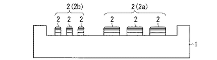
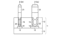
図1は、本発明の実施の形態1に係るパワー半導体装置1の構成を示す図である。当該パワー半導体装置1の上面(後述のプリント配線板3と対向する面)に、外部端子としての金属で形成された導電性の嵌入部材2が配設されている。各嵌入部材2は、パワー半導体装置1の上面から突出しており、それぞれの高さは全て同一となっている。
実施の形態2では、パワー半導体装置1の外部端子である嵌入部材2の構成の変形例を示す。図13は、実施の形態2に係る嵌入部材2の構成図である。当該嵌入部材2は、実施の形態1の嵌入部材2(図5)よりも幅が広く、プレスフィット部22を複数個(ここでは2個)有するものである。他の構成は、実施の形態1の嵌入部材2と同様である。
実施の形態3では、プリント配線板3に実装される嵌合部材4の構成の変形例を示す。図15はその一例を示す図であり、嵌合部材4の接合面42に位置合わせ用の突起43を設けたものである。図示は省略するが、嵌合部材4が固定されるパッド部31には、予めエッチング等により、突起43に対応する位置に位置合わせ用の窪みを設けておく。パッド部31と嵌合部材4との位置合わせが、突起43をパッド部31の窪みに合わせることによって行うことができるため、容易かつ正確な位置合わせが可能にある。
近年、高耐圧、低損失および高耐熱を実現できる次世代のスイッチング素子としては、炭化珪素(SiC)を代表とするワイドバンドギャップ半導体を用いた半導体素子が有望視されており、インバータなどのパワー半導体装置への適用が期待されている。ワイドバンドギャップ半導体としては、SiCの他、例えば窒化ガリウム(GaN)系材料、ダイヤモンドなどがある。
Claims (11)
- 電力用半導体装置とプリント配線板との接続機構であって、
前記電力用半導体装置は、
前記プリント配線板との対向面に突出した外部端子である導電性の嵌入部材を備え、
前記プリント配線板は、
当該プリント配線板のパッド部上に実装され、前記電力用半導体装置が当該プリント配線板に接続されるときに前記嵌入部材が挿入される導電性の嵌合部材を備え、
前記嵌入部材は、側面に凹部を有し、
前記嵌合部材は、内側面に弾性を有する凸部を有し、
前記嵌入部材が前記嵌合部材に挿入されたとき、前記嵌合部材の前記凸部が前記弾性により前記嵌入部材の前記凹部に圧接し、
前記電力用半導体装置は、
当該電力用半導体装置の表面を覆うモールド樹脂と、
前記モールド樹脂を貫通して前記電力用半導体装置の内部基板上の配線に達する開口部と、
前記開口部内に配設され、前記配線と接続した金属製のブッシュとを備え、
前記嵌入部材は、
前記ブッシュに挿入されたプレスフィット部を備える
ことを特徴とする電力用半導体装置とプリント配線板との接続機構。 - 前記凹部は、前記嵌入部材の互いに反対向きの側面にそれぞれ形成されており、
前記凸部は、前記嵌合部材の対向する内側面にそれぞれ形成されている
請求項1記載の電力用半導体装置とプリント配線板との接続機構。 - 前記凹部および前記凸部の表面は共にR形状である
請求項1または請求項2記載の電力用半導体装置とプリント配線板との接続機構。 - 前記嵌入部材は、前記プレスフィット部を複数個備える
請求項1記載の電力用半導体装置とプリント配線板との接続機構。 - 前記嵌入部材は、
折り曲がりのない1枚の金属板の側面の表面部分に前記凹部が設けられてなる形状となっている
請求項1から請求項4のいずれか一項記載の電力用半導体装置とプリント配線板との接続機構。 - 前記電力用半導体装置は、断面積の異なる複数の前記嵌入部材を備える
請求項1から請求項5のいずれか一項記載の電力用半導体装置とプリント配線板との接続機構。 - 前記電力用半導体装置は前記嵌入部材を複数個備え、当該複数の嵌入部材は全て同じ高さであり、
前記プリント配線板は前記嵌合部材を複数個備え、当該複数の嵌合部材は全て同じ高さである
請求項1から請求項6のいずれか一項記載の電力用半導体装置とプリント配線板との接続機構。 - 前記嵌合部材は、前記パッド部との接合面の部分が、他の部分より厚く形成されている
請求項1から請求項7のいずれか一項記載の電力用半導体装置とプリント配線板との接続機構。 - 前記嵌合部材は、前記パッド部との接合面に突起を有し、
前記パッド部の表面には、前記突起が挿入される窪みが形成されている
請求項1から請求項8のいずれか一項記載の電力用半導体装置とプリント配線板との接続機構。 - 前記嵌合部材は、前記パッド部との接合面に窪みを有し、
前記パッド部の表面には、前記窪みに挿入される突起が形成されている
請求項1から請求項8のいずれか一項記載の電力用半導体装置とプリント配線板との接続機構。 - 電力用半導体装置は、ワイドバンドギャップ半導体を用いて形成されている
請求項1から請求項10のいずれか一項記載の電力用半導体装置とプリント配線板との接続機構。
Priority Applications (4)
| Application Number | Priority Date | Filing Date | Title |
|---|---|---|---|
| JP2011009539A JP5599328B2 (ja) | 2011-01-20 | 2011-01-20 | 電力用半導体装置とプリント配線板との接続機構 |
| US13/223,600 US8575745B2 (en) | 2011-01-20 | 2011-09-01 | Power semiconductor device, printed wiring board, and mechanism for connecting the power semiconductor device and the printed wiring board |
| CN201110296956.7A CN102686013B (zh) | 2011-01-20 | 2011-09-30 | 功率半导体装置、印刷布线板和它们的连接机构 |
| DE102011087414.3A DE102011087414B4 (de) | 2011-01-20 | 2011-11-30 | Leistungshalbleitervorrichtung, gedruckte Leiterplatte und Mechanismus zum Verbinden der Leistungshalbleitervorrichtung und der gedruckten Leiterplatte |
Applications Claiming Priority (1)
| Application Number | Priority Date | Filing Date | Title |
|---|---|---|---|
| JP2011009539A JP5599328B2 (ja) | 2011-01-20 | 2011-01-20 | 電力用半導体装置とプリント配線板との接続機構 |
Publications (3)
| Publication Number | Publication Date |
|---|---|
| JP2012151019A JP2012151019A (ja) | 2012-08-09 |
| JP2012151019A5 JP2012151019A5 (ja) | 2013-07-18 |
| JP5599328B2 true JP5599328B2 (ja) | 2014-10-01 |
Family
ID=46510898
Family Applications (1)
| Application Number | Title | Priority Date | Filing Date |
|---|---|---|---|
| JP2011009539A Expired - Fee Related JP5599328B2 (ja) | 2011-01-20 | 2011-01-20 | 電力用半導体装置とプリント配線板との接続機構 |
Country Status (4)
| Country | Link |
|---|---|
| US (1) | US8575745B2 (ja) |
| JP (1) | JP5599328B2 (ja) |
| CN (1) | CN102686013B (ja) |
| DE (1) | DE102011087414B4 (ja) |
Families Citing this family (16)
| Publication number | Priority date | Publication date | Assignee | Title |
|---|---|---|---|---|
| JP2014049582A (ja) * | 2012-08-31 | 2014-03-17 | Mitsubishi Electric Corp | 半導体装置 |
| CN105074919B (zh) | 2013-02-26 | 2018-03-30 | 三菱电机株式会社 | 电力用半导体装置 |
| CN103367299B (zh) * | 2013-07-03 | 2017-02-15 | 株洲南车时代电气股份有限公司 | 半导体模块功率互联装置及其方法 |
| JP6117661B2 (ja) | 2013-09-19 | 2017-04-19 | 日立オートモティブシステムズ株式会社 | 電子制御装置 |
| US9706643B2 (en) | 2014-06-19 | 2017-07-11 | Panasonic Intellectual Property Management Co., Ltd. | Electronic device and method for manufacturing the same |
| DE102014116793B4 (de) | 2014-11-17 | 2018-03-08 | Infineon Technologies Ag | Leistungshalbleitermodul und Verfahren zur Herstellung eines Leistungshalbleitermoduls |
| CN107210279B (zh) * | 2015-05-21 | 2019-07-19 | 三菱电机株式会社 | 电力用半导体装置 |
| JP6380244B2 (ja) | 2015-06-15 | 2018-08-29 | 三菱電機株式会社 | 半導体装置、電力変換装置 |
| JP6455364B2 (ja) * | 2015-08-28 | 2019-01-23 | 三菱電機株式会社 | 半導体装置、インテリジェントパワーモジュールおよび電力変換装置 |
| JP6743542B2 (ja) | 2016-07-15 | 2020-08-19 | 富士電機株式会社 | 半導体装置及び半導体装置用ケース |
| JP6445066B2 (ja) * | 2017-03-22 | 2018-12-26 | 日立オートモティブシステムズ株式会社 | 電子制御装置 |
| JP6445068B2 (ja) * | 2017-03-23 | 2018-12-26 | 日立オートモティブシステムズ株式会社 | 電子制御装置 |
| EP3442080A1 (de) | 2017-08-09 | 2019-02-13 | HILTI Aktiengesellschaft | Steckkupplung für eine akkueinheit |
| CN107946273A (zh) * | 2017-12-22 | 2018-04-20 | 江苏宏微科技股份有限公司 | 一种插接功率模块封装装置 |
| US11901273B2 (en) * | 2021-07-26 | 2024-02-13 | Infineon Technologies Ag | Power module with press-fit contacts |
| DE102022118358A1 (de) | 2022-07-22 | 2024-01-25 | HARTING Electronics GmbH | Steckverbinder mit Transportsicherung für Gegenkontaktelemente |
Family Cites Families (34)
| Publication number | Priority date | Publication date | Assignee | Title |
|---|---|---|---|---|
| JPS507277B1 (ja) * | 1969-01-28 | 1975-03-24 | ||
| JPS52118595A (en) * | 1976-03-31 | 1977-10-05 | Matsushita Electric Works Ltd | Wiring track |
| JPS56104074U (ja) * | 1980-01-12 | 1981-08-14 | ||
| JPS58169878A (ja) | 1982-03-31 | 1983-10-06 | ケル株式会社 | Icソケツト用コンタクト |
| DE3675321D1 (de) * | 1985-08-16 | 1990-12-06 | Dai Ichi Seiko Co Ltd | Halbleiteranordnung mit packung vom steckerstifttyp. |
| US4750092A (en) * | 1985-11-20 | 1988-06-07 | Kollmorgen Technologies Corporation | Interconnection package suitable for electronic devices and methods for producing same |
| US4890152A (en) * | 1986-02-14 | 1989-12-26 | Matsushita Electric Works, Ltd. | Plastic molded chip carrier package and method of fabricating the same |
| DE3780764T2 (de) * | 1986-11-15 | 1992-12-24 | Matsushita Electric Works Ltd | Gegossenes kunststoff-chip-gehaeuse mit steckermuster. |
| US5144412A (en) * | 1987-02-19 | 1992-09-01 | Olin Corporation | Process for manufacturing plastic pin grid arrays and the product produced thereby |
| JPH01159369U (ja) | 1988-04-22 | 1989-11-06 | ||
| JPH0619169Y2 (ja) * | 1989-05-23 | 1994-05-18 | 住友電装株式会社 | ウェッジベースバルブ用ターミナル端子 |
| JPH0481365U (ja) * | 1990-11-27 | 1992-07-15 | ||
| JPH062594U (ja) * | 1992-06-16 | 1994-01-14 | 矢崎総業株式会社 | プラグターミナル |
| JPH07130417A (ja) * | 1993-10-29 | 1995-05-19 | Matsushita Electric Works Ltd | 電気接続装置 |
| JP2798605B2 (ja) | 1994-04-27 | 1998-09-17 | 日本電気株式会社 | 実装装置の製造方法 |
| JP2970463B2 (ja) * | 1995-03-31 | 1999-11-02 | 日本電気株式会社 | コネクタ |
| JP3908810B2 (ja) * | 1996-10-18 | 2007-04-25 | 富士通株式会社 | 光モジュール |
| JPH10123372A (ja) * | 1996-10-18 | 1998-05-15 | Fujitsu Ltd | 光モジュール |
| US5994648A (en) * | 1997-03-27 | 1999-11-30 | Ford Motor Company | Three-dimensional molded sockets for mechanical and electrical component attachment |
| WO1999002022A1 (en) | 1997-07-01 | 1999-01-14 | Koninklijke Philips Electronics N.V. | Printed circuit board with a leaded component and method of securing the component |
| JP3716108B2 (ja) * | 1998-10-20 | 2005-11-16 | 住友電装株式会社 | ウェッジベースバルブ装置 |
| DE10008572B4 (de) * | 2000-02-24 | 2007-08-09 | Infineon Technologies Ag | Verbindungseinrichtung für Leistungshalbleitermodule |
| JP2001351712A (ja) * | 2000-06-07 | 2001-12-21 | Auto Network Gijutsu Kenkyusho:Kk | 端子の構造 |
| TW515579U (en) | 2001-12-21 | 2002-12-21 | Hon Hai Prec Ind Co Ltd | Socket connector terminal |
| US7144792B2 (en) * | 2004-10-28 | 2006-12-05 | Woodward Governor Company | Method and apparatus for fabricating and connecting a semiconductor power switching device |
| JP4364135B2 (ja) * | 2005-02-07 | 2009-11-11 | 矢崎総業株式会社 | ジョイントコネクタの組み立て方法 |
| JP4444852B2 (ja) * | 2005-02-24 | 2010-03-31 | 三菱電機株式会社 | 同期電動機の固定子の製造方法及び同期電動機の固定子及び送風機 |
| JP2007109499A (ja) * | 2005-10-13 | 2007-04-26 | Fujitsu Ltd | コンタクト部材、コネクタ、基板、およびコネクタシステム |
| US8299603B2 (en) * | 2007-01-22 | 2012-10-30 | Mitsubishi Electric Corporation | Power semiconductor device |
| DE102007006212B4 (de) | 2007-02-08 | 2012-09-13 | Semikron Elektronik Gmbh & Co. Kg | Leistungshalbleitermodul mit Kontaktfedern |
| JP4879069B2 (ja) * | 2007-03-30 | 2012-02-15 | 矢崎総業株式会社 | メタルコア基板 |
| JP5313156B2 (ja) * | 2007-10-19 | 2013-10-09 | 日本発條株式会社 | 接続端子、半導体パッケージ、配線基板、コネクタ、およびマイクロコンタクタ |
| JP4567773B2 (ja) * | 2008-07-18 | 2010-10-20 | 三菱電機株式会社 | 電力用半導体装置 |
| JP4607995B2 (ja) * | 2008-11-28 | 2011-01-05 | 三菱電機株式会社 | 電力用半導体装置 |
-
2011
- 2011-01-20 JP JP2011009539A patent/JP5599328B2/ja not_active Expired - Fee Related
- 2011-09-01 US US13/223,600 patent/US8575745B2/en not_active Expired - Fee Related
- 2011-09-30 CN CN201110296956.7A patent/CN102686013B/zh not_active Expired - Fee Related
- 2011-11-30 DE DE102011087414.3A patent/DE102011087414B4/de active Active
Also Published As
| Publication number | Publication date |
|---|---|
| US20120187554A1 (en) | 2012-07-26 |
| US8575745B2 (en) | 2013-11-05 |
| CN102686013A (zh) | 2012-09-19 |
| DE102011087414B4 (de) | 2021-12-09 |
| JP2012151019A (ja) | 2012-08-09 |
| DE102011087414A1 (de) | 2012-07-26 |
| CN102686013B (zh) | 2016-02-03 |
Similar Documents
| Publication | Publication Date | Title |
|---|---|---|
| JP5599328B2 (ja) | 電力用半導体装置とプリント配線板との接続機構 | |
| JP5383621B2 (ja) | パワー半導体装置 | |
| US7331799B1 (en) | Stacked electronic component and fastening device thereof | |
| JP6157584B2 (ja) | 電力用半導体装置組み込み機器の製造方法および電力用半導体装置 | |
| JP4967447B2 (ja) | パワー半導体モジュール | |
| JP6316504B2 (ja) | 電力用半導体装置 | |
| JP5071405B2 (ja) | 電力用半導体装置 | |
| JP5156355B2 (ja) | 接触バネを有するパワー半導体モジュール | |
| JP5665729B2 (ja) | 電力用半導体装置 | |
| JP5011562B2 (ja) | 半導体装置およびその製造方法 | |
| US20100038758A1 (en) | Semiconductor module with two cooling surfaces and method | |
| JP5175535B2 (ja) | 接触バネを有するパワー半導体モジュール | |
| JP2017092185A (ja) | 半導体装置及びその製造方法 | |
| TWI344197B (en) | Semiconductor device | |
| CN112242374A (zh) | 半导体装置和半导体装置的制造方法 | |
| JP2014049582A (ja) | 半導体装置 | |
| CN110933900B (zh) | 电气设备和散热器 | |
| JP2002009217A (ja) | 樹脂封止型半導体装置 | |
| JP5561470B2 (ja) | ソケット、該ソケットと電子装置との接続構造、および半導体装置 | |
| JP4329187B2 (ja) | 半導体素子 | |
| JP2014123701A (ja) | 半導体装置 | |
| CN112154523B (zh) | 电阻器 | |
| WO2023100681A1 (ja) | 半導体装置 | |
| JP2017050478A (ja) | 抵抗器 | |
| JP2007141906A (ja) | 抵抗器 |
Legal Events
| Date | Code | Title | Description |
|---|---|---|---|
| A521 | Written amendment |
Free format text: JAPANESE INTERMEDIATE CODE: A523 Effective date: 20130531 |
|
| A621 | Written request for application examination |
Free format text: JAPANESE INTERMEDIATE CODE: A621 Effective date: 20130531 |
|
| A977 | Report on retrieval |
Free format text: JAPANESE INTERMEDIATE CODE: A971007 Effective date: 20140123 |
|
| A131 | Notification of reasons for refusal |
Free format text: JAPANESE INTERMEDIATE CODE: A131 Effective date: 20140304 |
|
| A521 | Written amendment |
Free format text: JAPANESE INTERMEDIATE CODE: A523 Effective date: 20140428 |
|
| TRDD | Decision of grant or rejection written | ||
| A01 | Written decision to grant a patent or to grant a registration (utility model) |
Free format text: JAPANESE INTERMEDIATE CODE: A01 Effective date: 20140715 |
|
| A61 | First payment of annual fees (during grant procedure) |
Free format text: JAPANESE INTERMEDIATE CODE: A61 Effective date: 20140812 |
|
| R150 | Certificate of patent or registration of utility model |
Ref document number: 5599328 Country of ref document: JP Free format text: JAPANESE INTERMEDIATE CODE: R150 |
|
| R250 | Receipt of annual fees |
Free format text: JAPANESE INTERMEDIATE CODE: R250 |
|
| R250 | Receipt of annual fees |
Free format text: JAPANESE INTERMEDIATE CODE: R250 |
|
| LAPS | Cancellation because of no payment of annual fees |