JP5436129B2 - Display device - Google Patents
Display device Download PDFInfo
- Publication number
- JP5436129B2 JP5436129B2 JP2009229350A JP2009229350A JP5436129B2 JP 5436129 B2 JP5436129 B2 JP 5436129B2 JP 2009229350 A JP2009229350 A JP 2009229350A JP 2009229350 A JP2009229350 A JP 2009229350A JP 5436129 B2 JP5436129 B2 JP 5436129B2
- Authority
- JP
- Japan
- Prior art keywords
- layer
- wiring
- thin film
- oxide semiconductor
- film transistor
- Prior art date
- Legal status (The legal status is an assumption and is not a legal conclusion. Google has not performed a legal analysis and makes no representation as to the accuracy of the status listed.)
- Active
Links
- 239000004065 semiconductor Substances 0.000 claims description 191
- 239000000758 substrate Substances 0.000 claims description 92
- 230000015572 biosynthetic process Effects 0.000 claims description 35
- 229910052733 gallium Inorganic materials 0.000 claims description 15
- IJGRMHOSHXDMSA-UHFFFAOYSA-N Atomic nitrogen Chemical compound N#N IJGRMHOSHXDMSA-UHFFFAOYSA-N 0.000 claims description 12
- 229910052725 zinc Inorganic materials 0.000 claims description 12
- 229910052738 indium Inorganic materials 0.000 claims description 11
- 229910052710 silicon Inorganic materials 0.000 claims description 8
- 239000010703 silicon Substances 0.000 claims description 7
- 229910052757 nitrogen Inorganic materials 0.000 claims description 6
- 239000010410 layer Substances 0.000 description 300
- 239000010408 film Substances 0.000 description 233
- 239000010409 thin film Substances 0.000 description 196
- 238000000034 method Methods 0.000 description 44
- 239000004973 liquid crystal related substance Substances 0.000 description 39
- 230000006870 function Effects 0.000 description 29
- 239000000463 material Substances 0.000 description 28
- 238000004544 sputter deposition Methods 0.000 description 23
- 230000001681 protective effect Effects 0.000 description 22
- 239000000123 paper Substances 0.000 description 21
- XKRFYHLGVUSROY-UHFFFAOYSA-N Argon Chemical compound [Ar] XKRFYHLGVUSROY-UHFFFAOYSA-N 0.000 description 20
- 239000012298 atmosphere Substances 0.000 description 19
- 239000003990 capacitor Substances 0.000 description 17
- 239000011241 protective layer Substances 0.000 description 17
- 238000005401 electroluminescence Methods 0.000 description 16
- 229910052760 oxygen Inorganic materials 0.000 description 16
- 239000011701 zinc Substances 0.000 description 16
- 239000013078 crystal Substances 0.000 description 15
- 239000001301 oxygen Substances 0.000 description 15
- VYPSYNLAJGMNEJ-UHFFFAOYSA-N Silicium dioxide Chemical compound O=[Si]=O VYPSYNLAJGMNEJ-UHFFFAOYSA-N 0.000 description 14
- QVGXLLKOCUKJST-UHFFFAOYSA-N atomic oxygen Chemical compound [O] QVGXLLKOCUKJST-UHFFFAOYSA-N 0.000 description 14
- 239000002245 particle Substances 0.000 description 14
- 229910052581 Si3N4 Inorganic materials 0.000 description 13
- XLOMVQKBTHCTTD-UHFFFAOYSA-N Zinc monoxide Chemical compound [Zn]=O XLOMVQKBTHCTTD-UHFFFAOYSA-N 0.000 description 13
- 238000005530 etching Methods 0.000 description 13
- 239000011521 glass Substances 0.000 description 13
- 239000011159 matrix material Substances 0.000 description 13
- HQVNEWCFYHHQES-UHFFFAOYSA-N silicon nitride Chemical compound N12[Si]34N5[Si]62N3[Si]51N64 HQVNEWCFYHHQES-UHFFFAOYSA-N 0.000 description 13
- 229910052814 silicon oxide Inorganic materials 0.000 description 13
- 229910052782 aluminium Inorganic materials 0.000 description 12
- 239000010936 titanium Substances 0.000 description 12
- 239000004020 conductor Substances 0.000 description 11
- 239000007789 gas Substances 0.000 description 11
- 229920005989 resin Polymers 0.000 description 11
- 239000011347 resin Substances 0.000 description 11
- XAGFODPZIPBFFR-UHFFFAOYSA-N aluminium Chemical compound [Al] XAGFODPZIPBFFR-UHFFFAOYSA-N 0.000 description 10
- 229910052786 argon Inorganic materials 0.000 description 10
- 239000000203 mixture Substances 0.000 description 10
- 230000008569 process Effects 0.000 description 10
- 239000000565 sealant Substances 0.000 description 10
- 238000010586 diagram Methods 0.000 description 9
- 238000010438 heat treatment Methods 0.000 description 9
- 238000004519 manufacturing process Methods 0.000 description 9
- 239000003094 microcapsule Substances 0.000 description 9
- 229910052751 metal Inorganic materials 0.000 description 8
- AMGQUBHHOARCQH-UHFFFAOYSA-N indium;oxotin Chemical compound [In].[Sn]=O AMGQUBHHOARCQH-UHFFFAOYSA-N 0.000 description 7
- 239000002356 single layer Substances 0.000 description 7
- XUIMIQQOPSSXEZ-UHFFFAOYSA-N Silicon Chemical compound [Si] XUIMIQQOPSSXEZ-UHFFFAOYSA-N 0.000 description 6
- 229910045601 alloy Inorganic materials 0.000 description 6
- 239000000956 alloy Substances 0.000 description 6
- 230000005684 electric field Effects 0.000 description 6
- 239000000945 filler Substances 0.000 description 6
- 239000001257 hydrogen Substances 0.000 description 6
- 229910052739 hydrogen Inorganic materials 0.000 description 6
- 239000012535 impurity Substances 0.000 description 6
- 229910003437 indium oxide Inorganic materials 0.000 description 6
- PJXISJQVUVHSOJ-UHFFFAOYSA-N indium(iii) oxide Chemical compound [O-2].[O-2].[O-2].[In+3].[In+3] PJXISJQVUVHSOJ-UHFFFAOYSA-N 0.000 description 6
- 238000003780 insertion Methods 0.000 description 6
- 230000037431 insertion Effects 0.000 description 6
- 239000002184 metal Substances 0.000 description 6
- 229910052719 titanium Inorganic materials 0.000 description 6
- 239000011787 zinc oxide Substances 0.000 description 6
- MYMOFIZGZYHOMD-UHFFFAOYSA-N Dioxygen Chemical compound O=O MYMOFIZGZYHOMD-UHFFFAOYSA-N 0.000 description 5
- UFHFLCQGNIYNRP-UHFFFAOYSA-N Hydrogen Chemical compound [H][H] UFHFLCQGNIYNRP-UHFFFAOYSA-N 0.000 description 5
- 239000011651 chromium Substances 0.000 description 5
- 229910001882 dioxygen Inorganic materials 0.000 description 5
- KPUWHANPEXNPJT-UHFFFAOYSA-N disiloxane Chemical class [SiH3]O[SiH3] KPUWHANPEXNPJT-UHFFFAOYSA-N 0.000 description 5
- 239000000428 dust Substances 0.000 description 5
- 239000011229 interlayer Substances 0.000 description 5
- TWNQGVIAIRXVLR-UHFFFAOYSA-N oxo(oxoalumanyloxy)alumane Chemical compound O=[Al]O[Al]=O TWNQGVIAIRXVLR-UHFFFAOYSA-N 0.000 description 5
- 239000012798 spherical particle Substances 0.000 description 5
- 229910005191 Ga 2 O 3 Inorganic materials 0.000 description 4
- 240000002329 Inga feuillei Species 0.000 description 4
- GWEVSGVZZGPLCZ-UHFFFAOYSA-N Titan oxide Chemical compound O=[Ti]=O GWEVSGVZZGPLCZ-UHFFFAOYSA-N 0.000 description 4
- RTAQQCXQSZGOHL-UHFFFAOYSA-N Titanium Chemical compound [Ti] RTAQQCXQSZGOHL-UHFFFAOYSA-N 0.000 description 4
- 229910007541 Zn O Inorganic materials 0.000 description 4
- 229920001940 conductive polymer Polymers 0.000 description 4
- PMHQVHHXPFUNSP-UHFFFAOYSA-M copper(1+);methylsulfanylmethane;bromide Chemical compound Br[Cu].CSC PMHQVHHXPFUNSP-UHFFFAOYSA-M 0.000 description 4
- 238000000151 deposition Methods 0.000 description 4
- 230000008021 deposition Effects 0.000 description 4
- 239000007788 liquid Substances 0.000 description 4
- 150000004767 nitrides Chemical class 0.000 description 4
- QGLKJKCYBOYXKC-UHFFFAOYSA-N nonaoxidotritungsten Chemical compound O=[W]1(=O)O[W](=O)(=O)O[W](=O)(=O)O1 QGLKJKCYBOYXKC-UHFFFAOYSA-N 0.000 description 4
- 230000003287 optical effect Effects 0.000 description 4
- 238000000206 photolithography Methods 0.000 description 4
- 238000009832 plasma treatment Methods 0.000 description 4
- 229920003023 plastic Polymers 0.000 description 4
- 239000004033 plastic Substances 0.000 description 4
- 229920006267 polyester film Polymers 0.000 description 4
- 239000000126 substance Substances 0.000 description 4
- OGIDPMRJRNCKJF-UHFFFAOYSA-N titanium oxide Inorganic materials [Ti]=O OGIDPMRJRNCKJF-UHFFFAOYSA-N 0.000 description 4
- 229910001930 tungsten oxide Inorganic materials 0.000 description 4
- YVTHLONGBIQYBO-UHFFFAOYSA-N zinc indium(3+) oxygen(2-) Chemical compound [O--].[Zn++].[In+3] YVTHLONGBIQYBO-UHFFFAOYSA-N 0.000 description 4
- -1 MgAg Inorganic materials 0.000 description 3
- NIXOWILDQLNWCW-UHFFFAOYSA-N acrylic acid group Chemical group C(C=C)(=O)O NIXOWILDQLNWCW-UHFFFAOYSA-N 0.000 description 3
- 229910021417 amorphous silicon Inorganic materials 0.000 description 3
- 238000004458 analytical method Methods 0.000 description 3
- 238000000137 annealing Methods 0.000 description 3
- 229910052804 chromium Inorganic materials 0.000 description 3
- 238000004891 communication Methods 0.000 description 3
- 238000011109 contamination Methods 0.000 description 3
- 238000001312 dry etching Methods 0.000 description 3
- 230000000694 effects Effects 0.000 description 3
- 230000005611 electricity Effects 0.000 description 3
- 230000005669 field effect Effects 0.000 description 3
- 238000007667 floating Methods 0.000 description 3
- 229910052742 iron Inorganic materials 0.000 description 3
- 230000007246 mechanism Effects 0.000 description 3
- 229910052750 molybdenum Inorganic materials 0.000 description 3
- 229910052759 nickel Inorganic materials 0.000 description 3
- 150000002894 organic compounds Chemical class 0.000 description 3
- 238000005192 partition Methods 0.000 description 3
- 229920002620 polyvinyl fluoride Polymers 0.000 description 3
- 239000000243 solution Substances 0.000 description 3
- 230000003068 static effect Effects 0.000 description 3
- 238000003860 storage Methods 0.000 description 3
- 229910052715 tantalum Inorganic materials 0.000 description 3
- 229910052721 tungsten Inorganic materials 0.000 description 3
- XLYOFNOQVPJJNP-UHFFFAOYSA-N water Chemical compound O XLYOFNOQVPJJNP-UHFFFAOYSA-N 0.000 description 3
- 238000001039 wet etching Methods 0.000 description 3
- UWCWUCKPEYNDNV-LBPRGKRZSA-N 2,6-dimethyl-n-[[(2s)-pyrrolidin-2-yl]methyl]aniline Chemical compound CC1=CC=CC(C)=C1NC[C@H]1NCCC1 UWCWUCKPEYNDNV-LBPRGKRZSA-N 0.000 description 2
- CURLTUGMZLYLDI-UHFFFAOYSA-N Carbon dioxide Chemical compound O=C=O CURLTUGMZLYLDI-UHFFFAOYSA-N 0.000 description 2
- VYZAMTAEIAYCRO-UHFFFAOYSA-N Chromium Chemical compound [Cr] VYZAMTAEIAYCRO-UHFFFAOYSA-N 0.000 description 2
- PXGOKWXKJXAPGV-UHFFFAOYSA-N Fluorine Chemical compound FF PXGOKWXKJXAPGV-UHFFFAOYSA-N 0.000 description 2
- VEXZGXHMUGYJMC-UHFFFAOYSA-N Hydrochloric acid Chemical compound Cl VEXZGXHMUGYJMC-UHFFFAOYSA-N 0.000 description 2
- ZOKXTWBITQBERF-UHFFFAOYSA-N Molybdenum Chemical compound [Mo] ZOKXTWBITQBERF-UHFFFAOYSA-N 0.000 description 2
- 229910052779 Neodymium Inorganic materials 0.000 description 2
- 239000004642 Polyimide Substances 0.000 description 2
- 230000001133 acceleration Effects 0.000 description 2
- 125000000217 alkyl group Chemical group 0.000 description 2
- DQXBYHZEEUGOBF-UHFFFAOYSA-N but-3-enoic acid;ethene Chemical compound C=C.OC(=O)CC=C DQXBYHZEEUGOBF-UHFFFAOYSA-N 0.000 description 2
- 230000015556 catabolic process Effects 0.000 description 2
- 230000001413 cellular effect Effects 0.000 description 2
- 239000010949 copper Substances 0.000 description 2
- 238000005520 cutting process Methods 0.000 description 2
- 239000005038 ethylene vinyl acetate Substances 0.000 description 2
- 230000005281 excited state Effects 0.000 description 2
- 230000001747 exhibiting effect Effects 0.000 description 2
- 239000000284 extract Substances 0.000 description 2
- 239000005262 ferroelectric liquid crystals (FLCs) Substances 0.000 description 2
- 239000011152 fibreglass Substances 0.000 description 2
- 239000011737 fluorine Substances 0.000 description 2
- 229910052731 fluorine Inorganic materials 0.000 description 2
- 238000001095 inductively coupled plasma mass spectrometry Methods 0.000 description 2
- 239000011261 inert gas Substances 0.000 description 2
- 238000002347 injection Methods 0.000 description 2
- 239000007924 injection Substances 0.000 description 2
- 239000011859 microparticle Substances 0.000 description 2
- 239000011733 molybdenum Substances 0.000 description 2
- QEFYFXOXNSNQGX-UHFFFAOYSA-N neodymium atom Chemical compound [Nd] QEFYFXOXNSNQGX-UHFFFAOYSA-N 0.000 description 2
- 239000012299 nitrogen atmosphere Substances 0.000 description 2
- 239000011368 organic material Substances 0.000 description 2
- BPUBBGLMJRNUCC-UHFFFAOYSA-N oxygen(2-);tantalum(5+) Chemical compound [O-2].[O-2].[O-2].[O-2].[O-2].[Ta+5].[Ta+5] BPUBBGLMJRNUCC-UHFFFAOYSA-N 0.000 description 2
- 239000000049 pigment Substances 0.000 description 2
- 229920001200 poly(ethylene-vinyl acetate) Polymers 0.000 description 2
- 229920002037 poly(vinyl butyral) polymer Polymers 0.000 description 2
- 229910021420 polycrystalline silicon Inorganic materials 0.000 description 2
- 229920001721 polyimide Polymers 0.000 description 2
- 229920000915 polyvinyl chloride Polymers 0.000 description 2
- 239000004800 polyvinyl chloride Substances 0.000 description 2
- 238000012545 processing Methods 0.000 description 2
- 230000004044 response Effects 0.000 description 2
- 238000005001 rutherford backscattering spectroscopy Methods 0.000 description 2
- 229910052706 scandium Inorganic materials 0.000 description 2
- SIXSYDAISGFNSX-UHFFFAOYSA-N scandium atom Chemical compound [Sc] SIXSYDAISGFNSX-UHFFFAOYSA-N 0.000 description 2
- 238000009751 slip forming Methods 0.000 description 2
- 239000002904 solvent Substances 0.000 description 2
- 125000006850 spacer group Chemical group 0.000 description 2
- 125000001424 substituent group Chemical group 0.000 description 2
- GUVRBAGPIYLISA-UHFFFAOYSA-N tantalum atom Chemical compound [Ta] GUVRBAGPIYLISA-UHFFFAOYSA-N 0.000 description 2
- 229910001936 tantalum oxide Inorganic materials 0.000 description 2
- 230000007704 transition Effects 0.000 description 2
- 229910052723 transition metal Inorganic materials 0.000 description 2
- WFKWXMTUELFFGS-UHFFFAOYSA-N tungsten Chemical compound [W] WFKWXMTUELFFGS-UHFFFAOYSA-N 0.000 description 2
- 239000010937 tungsten Substances 0.000 description 2
- 238000001771 vacuum deposition Methods 0.000 description 2
- 210000003462 vein Anatomy 0.000 description 2
- 239000004925 Acrylic resin Substances 0.000 description 1
- 229920000178 Acrylic resin Polymers 0.000 description 1
- 229910017073 AlLi Inorganic materials 0.000 description 1
- 239000004986 Cholesteric liquid crystals (ChLC) Substances 0.000 description 1
- RYGMFSIKBFXOCR-UHFFFAOYSA-N Copper Chemical compound [Cu] RYGMFSIKBFXOCR-UHFFFAOYSA-N 0.000 description 1
- 239000004593 Epoxy Substances 0.000 description 1
- GYHNNYVSQQEPJS-UHFFFAOYSA-N Gallium Chemical compound [Ga] GYHNNYVSQQEPJS-UHFFFAOYSA-N 0.000 description 1
- 206010052128 Glare Diseases 0.000 description 1
- DGAQECJNVWCQMB-PUAWFVPOSA-M Ilexoside XXIX Chemical compound C[C@@H]1CC[C@@]2(CC[C@@]3(C(=CC[C@H]4[C@]3(CC[C@@H]5[C@@]4(CC[C@@H](C5(C)C)OS(=O)(=O)[O-])C)C)[C@@H]2[C@]1(C)O)C)C(=O)O[C@H]6[C@@H]([C@H]([C@@H]([C@H](O6)CO)O)O)O.[Na+] DGAQECJNVWCQMB-PUAWFVPOSA-M 0.000 description 1
- OAICVXFJPJFONN-UHFFFAOYSA-N Phosphorus Chemical compound [P] OAICVXFJPJFONN-UHFFFAOYSA-N 0.000 description 1
- 239000004952 Polyamide Substances 0.000 description 1
- 229910003902 SiCl 4 Inorganic materials 0.000 description 1
- 229910002808 Si–O–Si Inorganic materials 0.000 description 1
- 229910006404 SnO 2 Inorganic materials 0.000 description 1
- 238000002441 X-ray diffraction Methods 0.000 description 1
- HCHKCACWOHOZIP-UHFFFAOYSA-N Zinc Chemical compound [Zn] HCHKCACWOHOZIP-UHFFFAOYSA-N 0.000 description 1
- GDFCWFBWQUEQIJ-UHFFFAOYSA-N [B].[P] Chemical compound [B].[P] GDFCWFBWQUEQIJ-UHFFFAOYSA-N 0.000 description 1
- 230000004913 activation Effects 0.000 description 1
- 239000005407 aluminoborosilicate glass Substances 0.000 description 1
- 239000005354 aluminosilicate glass Substances 0.000 description 1
- 150000004945 aromatic hydrocarbons Chemical class 0.000 description 1
- 125000003118 aryl group Chemical group 0.000 description 1
- 229910052788 barium Inorganic materials 0.000 description 1
- DSAJWYNOEDNPEQ-UHFFFAOYSA-N barium atom Chemical compound [Ba] DSAJWYNOEDNPEQ-UHFFFAOYSA-N 0.000 description 1
- QVQLCTNNEUAWMS-UHFFFAOYSA-N barium oxide Chemical compound [Ba]=O QVQLCTNNEUAWMS-UHFFFAOYSA-N 0.000 description 1
- 230000008901 benefit Effects 0.000 description 1
- UMIVXZPTRXBADB-UHFFFAOYSA-N benzocyclobutene Chemical compound C1=CC=C2CCC2=C1 UMIVXZPTRXBADB-UHFFFAOYSA-N 0.000 description 1
- 230000002457 bidirectional effect Effects 0.000 description 1
- 239000011230 binding agent Substances 0.000 description 1
- KGBXLFKZBHKPEV-UHFFFAOYSA-N boric acid Chemical compound OB(O)O KGBXLFKZBHKPEV-UHFFFAOYSA-N 0.000 description 1
- 239000004327 boric acid Substances 0.000 description 1
- 239000005380 borophosphosilicate glass Substances 0.000 description 1
- 239000005388 borosilicate glass Substances 0.000 description 1
- 239000001569 carbon dioxide Substances 0.000 description 1
- 229910002092 carbon dioxide Inorganic materials 0.000 description 1
- 239000000969 carrier Substances 0.000 description 1
- 239000000919 ceramic Substances 0.000 description 1
- 230000003098 cholesteric effect Effects 0.000 description 1
- 238000004040 coloring Methods 0.000 description 1
- 239000002131 composite material Substances 0.000 description 1
- 239000000356 contaminant Substances 0.000 description 1
- 239000002872 contrast media Substances 0.000 description 1
- 229920001577 copolymer Polymers 0.000 description 1
- 229910052802 copper Inorganic materials 0.000 description 1
- 238000005260 corrosion Methods 0.000 description 1
- 230000007797 corrosion Effects 0.000 description 1
- 229910021419 crystalline silicon Inorganic materials 0.000 description 1
- 238000002425 crystallisation Methods 0.000 description 1
- 230000008025 crystallization Effects 0.000 description 1
- 230000007547 defect Effects 0.000 description 1
- 230000002950 deficient Effects 0.000 description 1
- 238000007872 degassing Methods 0.000 description 1
- 238000013461 design Methods 0.000 description 1
- 238000001514 detection method Methods 0.000 description 1
- 239000003989 dielectric material Substances 0.000 description 1
- 238000009792 diffusion process Methods 0.000 description 1
- AJNVQOSZGJRYEI-UHFFFAOYSA-N digallium;oxygen(2-) Chemical compound [O-2].[O-2].[O-2].[Ga+3].[Ga+3] AJNVQOSZGJRYEI-UHFFFAOYSA-N 0.000 description 1
- 238000006073 displacement reaction Methods 0.000 description 1
- 230000009977 dual effect Effects 0.000 description 1
- 239000003822 epoxy resin Substances 0.000 description 1
- 239000004744 fabric Substances 0.000 description 1
- 239000011888 foil Substances 0.000 description 1
- 230000005283 ground state Effects 0.000 description 1
- 229910000449 hafnium oxide Inorganic materials 0.000 description 1
- WIHZLLGSGQNAGK-UHFFFAOYSA-N hafnium(4+);oxygen(2-) Chemical compound [O-2].[O-2].[Hf+4] WIHZLLGSGQNAGK-UHFFFAOYSA-N 0.000 description 1
- 239000001307 helium Substances 0.000 description 1
- 229910052734 helium Inorganic materials 0.000 description 1
- SWQJXJOGLNCZEY-UHFFFAOYSA-N helium atom Chemical compound [He] SWQJXJOGLNCZEY-UHFFFAOYSA-N 0.000 description 1
- 230000005525 hole transport Effects 0.000 description 1
- 150000002431 hydrogen Chemical class 0.000 description 1
- 125000002887 hydroxy group Chemical group [H]O* 0.000 description 1
- APFVFJFRJDLVQX-UHFFFAOYSA-N indium atom Chemical compound [In] APFVFJFRJDLVQX-UHFFFAOYSA-N 0.000 description 1
- 150000002484 inorganic compounds Chemical class 0.000 description 1
- 229910010272 inorganic material Inorganic materials 0.000 description 1
- 239000012212 insulator Substances 0.000 description 1
- 150000002500 ions Chemical class 0.000 description 1
- 238000003475 lamination Methods 0.000 description 1
- 238000005224 laser annealing Methods 0.000 description 1
- 239000000395 magnesium oxide Substances 0.000 description 1
- CPLXHLVBOLITMK-UHFFFAOYSA-N magnesium oxide Inorganic materials [Mg]=O CPLXHLVBOLITMK-UHFFFAOYSA-N 0.000 description 1
- AXZKOIWUVFPNLO-UHFFFAOYSA-N magnesium;oxygen(2-) Chemical compound [O-2].[Mg+2] AXZKOIWUVFPNLO-UHFFFAOYSA-N 0.000 description 1
- 239000000696 magnetic material Substances 0.000 description 1
- 230000005389 magnetism Effects 0.000 description 1
- 238000000838 magnetophoresis Methods 0.000 description 1
- 229910052748 manganese Inorganic materials 0.000 description 1
- 238000005259 measurement Methods 0.000 description 1
- 238000000691 measurement method Methods 0.000 description 1
- 229910021645 metal ion Inorganic materials 0.000 description 1
- 239000007769 metal material Substances 0.000 description 1
- 238000012986 modification Methods 0.000 description 1
- 230000004048 modification Effects 0.000 description 1
- 239000002159 nanocrystal Substances 0.000 description 1
- 238000007645 offset printing Methods 0.000 description 1
- 239000012788 optical film Substances 0.000 description 1
- AHLBNYSZXLDEJQ-FWEHEUNISA-N orlistat Chemical compound CCCCCCCCCCC[C@H](OC(=O)[C@H](CC(C)C)NC=O)C[C@@H]1OC(=O)[C@H]1CCCCCC AHLBNYSZXLDEJQ-FWEHEUNISA-N 0.000 description 1
- 230000003647 oxidation Effects 0.000 description 1
- 238000007254 oxidation reaction Methods 0.000 description 1
- SIWVEOZUMHYXCS-UHFFFAOYSA-N oxo(oxoyttriooxy)yttrium Chemical compound O=[Y]O[Y]=O SIWVEOZUMHYXCS-UHFFFAOYSA-N 0.000 description 1
- 230000002093 peripheral effect Effects 0.000 description 1
- 229910052698 phosphorus Inorganic materials 0.000 description 1
- 239000011574 phosphorus Substances 0.000 description 1
- 230000000704 physical effect Effects 0.000 description 1
- 238000005268 plasma chemical vapour deposition Methods 0.000 description 1
- 229920002647 polyamide Polymers 0.000 description 1
- 229920000767 polyaniline Polymers 0.000 description 1
- 229920000647 polyepoxide Polymers 0.000 description 1
- 229920000128 polypyrrole Polymers 0.000 description 1
- 229920001296 polysiloxane Polymers 0.000 description 1
- 229920000123 polythiophene Polymers 0.000 description 1
- 238000011002 quantification Methods 0.000 description 1
- 239000010453 quartz Substances 0.000 description 1
- 230000005855 radiation Effects 0.000 description 1
- 239000012495 reaction gas Substances 0.000 description 1
- 238000005546 reactive sputtering Methods 0.000 description 1
- 230000008707 rearrangement Effects 0.000 description 1
- 230000006798 recombination Effects 0.000 description 1
- 238000005215 recombination Methods 0.000 description 1
- 238000007650 screen-printing Methods 0.000 description 1
- 239000003566 sealing material Substances 0.000 description 1
- 229920002050 silicone resin Polymers 0.000 description 1
- 239000011734 sodium Substances 0.000 description 1
- 229910052708 sodium Inorganic materials 0.000 description 1
- 238000004528 spin coating Methods 0.000 description 1
- 238000005507 spraying Methods 0.000 description 1
- 239000010935 stainless steel Substances 0.000 description 1
- 229910001220 stainless steel Inorganic materials 0.000 description 1
- 239000007858 starting material Substances 0.000 description 1
- 229920001187 thermosetting polymer Polymers 0.000 description 1
- 150000003608 titanium Chemical class 0.000 description 1
- 229910000314 transition metal oxide Inorganic materials 0.000 description 1
- 150000003624 transition metals Chemical class 0.000 description 1
- 238000002834 transmittance Methods 0.000 description 1
- OYQCBJZGELKKPM-UHFFFAOYSA-N zinc indium(3+) oxygen(2-) Chemical compound [O-2].[Zn+2].[O-2].[In+3] OYQCBJZGELKKPM-UHFFFAOYSA-N 0.000 description 1
Images


Classifications
-
- H—ELECTRICITY
- H01—ELECTRIC ELEMENTS
- H01L—SEMICONDUCTOR DEVICES NOT COVERED BY CLASS H10
- H01L29/00—Semiconductor devices specially adapted for rectifying, amplifying, oscillating or switching and having potential barriers; Capacitors or resistors having potential barriers, e.g. a PN-junction depletion layer or carrier concentration layer; Details of semiconductor bodies or of electrodes thereof ; Multistep manufacturing processes therefor
- H01L29/66—Types of semiconductor device ; Multistep manufacturing processes therefor
- H01L29/68—Types of semiconductor device ; Multistep manufacturing processes therefor controllable by only the electric current supplied, or only the electric potential applied, to an electrode which does not carry the current to be rectified, amplified or switched
- H01L29/76—Unipolar devices, e.g. field effect transistors
- H01L29/772—Field effect transistors
- H01L29/78—Field effect transistors with field effect produced by an insulated gate
- H01L29/786—Thin film transistors, i.e. transistors with a channel being at least partly a thin film
- H01L29/7869—Thin film transistors, i.e. transistors with a channel being at least partly a thin film having a semiconductor body comprising an oxide semiconductor material, e.g. zinc oxide, copper aluminium oxide, cadmium stannate
-
- G—PHYSICS
- G02—OPTICS
- G02F—OPTICAL DEVICES OR ARRANGEMENTS FOR THE CONTROL OF LIGHT BY MODIFICATION OF THE OPTICAL PROPERTIES OF THE MEDIA OF THE ELEMENTS INVOLVED THEREIN; NON-LINEAR OPTICS; FREQUENCY-CHANGING OF LIGHT; OPTICAL LOGIC ELEMENTS; OPTICAL ANALOGUE/DIGITAL CONVERTERS
- G02F1/00—Devices or arrangements for the control of the intensity, colour, phase, polarisation or direction of light arriving from an independent light source, e.g. switching, gating or modulating; Non-linear optics
- G02F1/01—Devices or arrangements for the control of the intensity, colour, phase, polarisation or direction of light arriving from an independent light source, e.g. switching, gating or modulating; Non-linear optics for the control of the intensity, phase, polarisation or colour
- G02F1/13—Devices or arrangements for the control of the intensity, colour, phase, polarisation or direction of light arriving from an independent light source, e.g. switching, gating or modulating; Non-linear optics for the control of the intensity, phase, polarisation or colour based on liquid crystals, e.g. single liquid crystal display cells
- G02F1/133—Constructional arrangements; Operation of liquid crystal cells; Circuit arrangements
- G02F1/136—Liquid crystal cells structurally associated with a semi-conducting layer or substrate, e.g. cells forming part of an integrated circuit
- G02F1/1362—Active matrix addressed cells
- G02F1/136204—Arrangements to prevent high voltage or static electricity failures
-
- G—PHYSICS
- G02—OPTICS
- G02F—OPTICAL DEVICES OR ARRANGEMENTS FOR THE CONTROL OF LIGHT BY MODIFICATION OF THE OPTICAL PROPERTIES OF THE MEDIA OF THE ELEMENTS INVOLVED THEREIN; NON-LINEAR OPTICS; FREQUENCY-CHANGING OF LIGHT; OPTICAL LOGIC ELEMENTS; OPTICAL ANALOGUE/DIGITAL CONVERTERS
- G02F1/00—Devices or arrangements for the control of the intensity, colour, phase, polarisation or direction of light arriving from an independent light source, e.g. switching, gating or modulating; Non-linear optics
- G02F1/01—Devices or arrangements for the control of the intensity, colour, phase, polarisation or direction of light arriving from an independent light source, e.g. switching, gating or modulating; Non-linear optics for the control of the intensity, phase, polarisation or colour
- G02F1/13—Devices or arrangements for the control of the intensity, colour, phase, polarisation or direction of light arriving from an independent light source, e.g. switching, gating or modulating; Non-linear optics for the control of the intensity, phase, polarisation or colour based on liquid crystals, e.g. single liquid crystal display cells
- G02F1/133—Constructional arrangements; Operation of liquid crystal cells; Circuit arrangements
- G02F1/136—Liquid crystal cells structurally associated with a semi-conducting layer or substrate, e.g. cells forming part of an integrated circuit
- G02F1/1362—Active matrix addressed cells
- G02F1/1368—Active matrix addressed cells in which the switching element is a three-electrode device
-
- H—ELECTRICITY
- H01—ELECTRIC ELEMENTS
- H01L—SEMICONDUCTOR DEVICES NOT COVERED BY CLASS H10
- H01L27/00—Devices consisting of a plurality of semiconductor or other solid-state components formed in or on a common substrate
- H01L27/02—Devices consisting of a plurality of semiconductor or other solid-state components formed in or on a common substrate including semiconductor components specially adapted for rectifying, oscillating, amplifying or switching and having potential barriers; including integrated passive circuit elements having potential barriers
- H01L27/0203—Particular design considerations for integrated circuits
- H01L27/0248—Particular design considerations for integrated circuits for electrical or thermal protection, e.g. electrostatic discharge [ESD] protection
-
- H—ELECTRICITY
- H01—ELECTRIC ELEMENTS
- H01L—SEMICONDUCTOR DEVICES NOT COVERED BY CLASS H10
- H01L27/00—Devices consisting of a plurality of semiconductor or other solid-state components formed in or on a common substrate
- H01L27/02—Devices consisting of a plurality of semiconductor or other solid-state components formed in or on a common substrate including semiconductor components specially adapted for rectifying, oscillating, amplifying or switching and having potential barriers; including integrated passive circuit elements having potential barriers
- H01L27/12—Devices consisting of a plurality of semiconductor or other solid-state components formed in or on a common substrate including semiconductor components specially adapted for rectifying, oscillating, amplifying or switching and having potential barriers; including integrated passive circuit elements having potential barriers the substrate being other than a semiconductor body, e.g. an insulating body
- H01L27/1214—Devices consisting of a plurality of semiconductor or other solid-state components formed in or on a common substrate including semiconductor components specially adapted for rectifying, oscillating, amplifying or switching and having potential barriers; including integrated passive circuit elements having potential barriers the substrate being other than a semiconductor body, e.g. an insulating body comprising a plurality of TFTs formed on a non-semiconducting substrate, e.g. driving circuits for AMLCDs
- H01L27/1222—Devices consisting of a plurality of semiconductor or other solid-state components formed in or on a common substrate including semiconductor components specially adapted for rectifying, oscillating, amplifying or switching and having potential barriers; including integrated passive circuit elements having potential barriers the substrate being other than a semiconductor body, e.g. an insulating body comprising a plurality of TFTs formed on a non-semiconducting substrate, e.g. driving circuits for AMLCDs with a particular composition, shape or crystalline structure of the active layer
- H01L27/1225—Devices consisting of a plurality of semiconductor or other solid-state components formed in or on a common substrate including semiconductor components specially adapted for rectifying, oscillating, amplifying or switching and having potential barriers; including integrated passive circuit elements having potential barriers the substrate being other than a semiconductor body, e.g. an insulating body comprising a plurality of TFTs formed on a non-semiconducting substrate, e.g. driving circuits for AMLCDs with a particular composition, shape or crystalline structure of the active layer with semiconductor materials not belonging to the group IV of the periodic table, e.g. InGaZnO
-
- H—ELECTRICITY
- H01—ELECTRIC ELEMENTS
- H01L—SEMICONDUCTOR DEVICES NOT COVERED BY CLASS H10
- H01L27/00—Devices consisting of a plurality of semiconductor or other solid-state components formed in or on a common substrate
- H01L27/02—Devices consisting of a plurality of semiconductor or other solid-state components formed in or on a common substrate including semiconductor components specially adapted for rectifying, oscillating, amplifying or switching and having potential barriers; including integrated passive circuit elements having potential barriers
- H01L27/12—Devices consisting of a plurality of semiconductor or other solid-state components formed in or on a common substrate including semiconductor components specially adapted for rectifying, oscillating, amplifying or switching and having potential barriers; including integrated passive circuit elements having potential barriers the substrate being other than a semiconductor body, e.g. an insulating body
- H01L27/1214—Devices consisting of a plurality of semiconductor or other solid-state components formed in or on a common substrate including semiconductor components specially adapted for rectifying, oscillating, amplifying or switching and having potential barriers; including integrated passive circuit elements having potential barriers the substrate being other than a semiconductor body, e.g. an insulating body comprising a plurality of TFTs formed on a non-semiconducting substrate, e.g. driving circuits for AMLCDs
- H01L27/124—Devices consisting of a plurality of semiconductor or other solid-state components formed in or on a common substrate including semiconductor components specially adapted for rectifying, oscillating, amplifying or switching and having potential barriers; including integrated passive circuit elements having potential barriers the substrate being other than a semiconductor body, e.g. an insulating body comprising a plurality of TFTs formed on a non-semiconducting substrate, e.g. driving circuits for AMLCDs with a particular composition, shape or layout of the wiring layers specially adapted to the circuit arrangement, e.g. scanning lines in LCD pixel circuits
-
- H—ELECTRICITY
- H01—ELECTRIC ELEMENTS
- H01L—SEMICONDUCTOR DEVICES NOT COVERED BY CLASS H10
- H01L29/00—Semiconductor devices specially adapted for rectifying, amplifying, oscillating or switching and having potential barriers; Capacitors or resistors having potential barriers, e.g. a PN-junction depletion layer or carrier concentration layer; Details of semiconductor bodies or of electrodes thereof ; Multistep manufacturing processes therefor
- H01L29/66—Types of semiconductor device ; Multistep manufacturing processes therefor
- H01L29/68—Types of semiconductor device ; Multistep manufacturing processes therefor controllable by only the electric current supplied, or only the electric potential applied, to an electrode which does not carry the current to be rectified, amplified or switched
- H01L29/76—Unipolar devices, e.g. field effect transistors
- H01L29/772—Field effect transistors
- H01L29/78—Field effect transistors with field effect produced by an insulated gate
- H01L29/786—Thin film transistors, i.e. transistors with a channel being at least partly a thin film
- H01L29/78606—Thin film transistors, i.e. transistors with a channel being at least partly a thin film with supplementary region or layer in the thin film or in the insulated bulk substrate supporting it for controlling or increasing the safety of the device
- H01L29/78618—Thin film transistors, i.e. transistors with a channel being at least partly a thin film with supplementary region or layer in the thin film or in the insulated bulk substrate supporting it for controlling or increasing the safety of the device characterised by the drain or the source properties, e.g. the doping structure, the composition, the sectional shape or the contact structure
-
- H—ELECTRICITY
- H01—ELECTRIC ELEMENTS
- H01L—SEMICONDUCTOR DEVICES NOT COVERED BY CLASS H10
- H01L29/00—Semiconductor devices specially adapted for rectifying, amplifying, oscillating or switching and having potential barriers; Capacitors or resistors having potential barriers, e.g. a PN-junction depletion layer or carrier concentration layer; Details of semiconductor bodies or of electrodes thereof ; Multistep manufacturing processes therefor
- H01L29/66—Types of semiconductor device ; Multistep manufacturing processes therefor
- H01L29/68—Types of semiconductor device ; Multistep manufacturing processes therefor controllable by only the electric current supplied, or only the electric potential applied, to an electrode which does not carry the current to be rectified, amplified or switched
- H01L29/76—Unipolar devices, e.g. field effect transistors
- H01L29/772—Field effect transistors
- H01L29/78—Field effect transistors with field effect produced by an insulated gate
- H01L29/786—Thin film transistors, i.e. transistors with a channel being at least partly a thin film
- H01L29/78696—Thin film transistors, i.e. transistors with a channel being at least partly a thin film characterised by the structure of the channel, e.g. multichannel, transverse or longitudinal shape, length or width, doping structure, or the overlap or alignment between the channel and the gate, the source or the drain, or the contacting structure of the channel
-
- H—ELECTRICITY
- H01—ELECTRIC ELEMENTS
- H01L—SEMICONDUCTOR DEVICES NOT COVERED BY CLASS H10
- H01L33/00—Semiconductor devices having potential barriers specially adapted for light emission; Processes or apparatus specially adapted for the manufacture or treatment thereof or of parts thereof; Details thereof
- H01L33/0004—Devices characterised by their operation
- H01L33/0041—Devices characterised by their operation characterised by field-effect operation
-
- H—ELECTRICITY
- H01—ELECTRIC ELEMENTS
- H01L—SEMICONDUCTOR DEVICES NOT COVERED BY CLASS H10
- H01L2924/00—Indexing scheme for arrangements or methods for connecting or disconnecting semiconductor or solid-state bodies as covered by H01L24/00
- H01L2924/0001—Technical content checked by a classifier
- H01L2924/0002—Not covered by any one of groups H01L24/00, H01L24/00 and H01L2224/00
Landscapes
- Engineering & Computer Science (AREA)
- Physics & Mathematics (AREA)
- Power Engineering (AREA)
- Microelectronics & Electronic Packaging (AREA)
- General Physics & Mathematics (AREA)
- Computer Hardware Design (AREA)
- Condensed Matter Physics & Semiconductors (AREA)
- Nonlinear Science (AREA)
- Crystallography & Structural Chemistry (AREA)
- Chemical & Material Sciences (AREA)
- Mathematical Physics (AREA)
- Optics & Photonics (AREA)
- Ceramic Engineering (AREA)
- Manufacturing & Machinery (AREA)
- Thin Film Transistor (AREA)
- Liquid Crystal (AREA)
- Devices For Indicating Variable Information By Combining Individual Elements (AREA)
- Electroluminescent Light Sources (AREA)
- Semiconductor Integrated Circuits (AREA)
- Metal-Oxide And Bipolar Metal-Oxide Semiconductor Integrated Circuits (AREA)
- Electrochromic Elements, Electrophoresis, Or Variable Reflection Or Absorption Elements (AREA)
- Electrodes Of Semiconductors (AREA)
- Internal Circuitry In Semiconductor Integrated Circuit Devices (AREA)
Description
本発明は、酸化物半導体を用いる表示装置に関する。 The present invention relates to a display device using an oxide semiconductor.
液晶表示装置に代表されるように、ガラス基板等の平板に形成される薄膜トランジスタは、アモルファスシリコン、多結晶シリコンによって作製されている。アモルファスシリコンを用いた薄膜トランジスタは、電界効果移動度が低いもののガラス基板の大面積化に対応することができ、一方、結晶シリコンを用いた薄膜トランジスタは、電界効果移動度は高いものの、レーザアニール等の結晶化工程が必要であり、ガラス基板の大面積化には必ずしも適応しないといった特性を有している。 As represented by a liquid crystal display device, a thin film transistor formed on a flat plate such as a glass substrate is made of amorphous silicon or polycrystalline silicon. A thin film transistor using amorphous silicon can cope with an increase in the area of a glass substrate although the field effect mobility is low. On the other hand, a thin film transistor using crystalline silicon has a high field effect mobility but is not suitable for laser annealing or the like. A crystallization process is required, and it has a characteristic that it is not necessarily adapted to an increase in area of a glass substrate.
これに対し、酸化物半導体を用いて薄膜トランジスタを作製し、電子デバイスや光デバイスに応用する技術が注目されている。例えば、酸化物半導体膜として酸化亜鉛(ZnO)や、インジウム、ガリウム、及び亜鉛を含む酸化物半導体を用いて薄膜トランジスタを作製し、画像表示装置のスイッチング素子などに用いる技術が特許文献1及び特許文献2で開示されている。
In contrast, a technique in which a thin film transistor is manufactured using an oxide semiconductor and applied to an electronic device or an optical device has attracted attention. For example, a technique in which a thin film transistor is manufactured using an oxide semiconductor containing zinc oxide (ZnO) or indium, gallium, and zinc as an oxide semiconductor film and used for a switching element of an image display device is disclosed in
酸化物半導体をチャネル形成領域とする薄膜トランジスタは、アモルファスシリコンを用いた薄膜トランジスタよりも動作速度が速く、多結晶シリコンを用いた薄膜トランジスタよりも製造工程が簡単であるといった特性を有している。すなわち、酸化物半導体を用いることによって、プロセス温度が室温から300℃以下の低温であっても、電界効果移動度が高い薄膜トランジスタを作製することが可能である。 A thin film transistor using an oxide semiconductor as a channel formation region has characteristics such that an operation speed is higher than that of a thin film transistor using amorphous silicon and a manufacturing process is simpler than that of a thin film transistor using polycrystalline silicon. That is, by using an oxide semiconductor, a thin film transistor with high field-effect mobility can be manufactured even when the process temperature is from room temperature to 300 ° C. or lower.
動作特性に優れ低温で製造可能な酸化物半導体を用いた表示装置の特性を活かし、信頼性を保証するためには、適切な構成を備えた保護回路等が必要となる。また、表示装置の小型化を図る上で、保護回路の占有面積を小さくすることが必要になってくる。 In order to ensure reliability by utilizing the characteristics of a display device using an oxide semiconductor that has excellent operating characteristics and can be manufactured at low temperatures, a protection circuit or the like having an appropriate configuration is required. Further, in order to reduce the size of the display device, it is necessary to reduce the area occupied by the protection circuit.
本発明は、保護回路として適した構造を提供することを目的の一とする。 An object of the present invention is to provide a structure suitable as a protection circuit.
本発明は、酸化物半導体の他、絶縁膜及び導電膜を積層して作製される各種用途の表示装置において、保護回路の機能を高め動作の安定化と保護回路の占有面積の小型化を図ることを目的の一とする。 The present invention aims to improve the function of the protection circuit, stabilize the operation, and reduce the area occupied by the protection circuit in display devices for various uses that are manufactured by stacking an insulating film and a conductive film in addition to an oxide semiconductor. One of the purposes.
本発明の一態様は、酸化物半導体を用いて構成される非線形素子で保護回路が形成された表示装置である。この非線形素子は酸素含有量がことなる酸化物半導体を組み合わせて構成されている。また、この非線形素子が有する第1配線層及び第2配線層の少なくとも一方が、ゲート電極もしくはゲート配線層と同じ工程で形成された配線に直接接続している。 One embodiment of the present invention is a display device in which a protective circuit is formed using a nonlinear element including an oxide semiconductor. This nonlinear element is formed by combining oxide semiconductors having different oxygen contents. Further, at least one of the first wiring layer and the second wiring layer included in the nonlinear element is directly connected to a wiring formed in the same process as the gate electrode or the gate wiring layer.
本発明の例示的な一態様は、絶縁表面を有する基板上に走査線と信号線が交差して設けられ、画素電極がマトリクス状に配列する画素部と、該画素部の外側領域に酸化物半導体で形成された非線形素子を有する表示装置である。画素部は、第1酸化物半導体層にチャネル形成領域が形成される薄膜トランジスタを有する。画素部の薄膜トランジスタは、走査線と接続するゲート電極と、信号線と接続し第1酸化物半導体層に接する第1配線層と、画素電極と接続し第1酸化物半導体層に接する第2配線層とを有する。基板の周辺部に配設される信号入力端子と画素部の間には非線形素子が設けられている。非線形素子は、ゲート電極及び該ゲート電極を被覆するゲート絶縁層と、前記ゲート絶縁層上において前記ゲート電極と重畳する第1酸化物半導体層と、前記第1酸化物半導体層のチャネル形成領域と重なる領域を覆うチャネル保護層と、前記チャネル保護層上において前記ゲート電極と端部が重畳し、第1酸化物半導体層と接する、導電層と第2酸化物半導体層が積層された第1配線層及び第2配線層とを有している。また、第1配線層及び第2配線層の導電層が第2酸化物半導体層を介して第1酸化物半導体層と接し、非線形素子のゲート電極は走査線又は信号線と接続され、非線形素子の第1配線層又は第2配線層がゲート電極の電位が印加されるようにゲート電極もしくはゲート電極と同じ層で形成した配線層と直接接続されている。 One exemplary embodiment of the present invention is a pixel portion in which a scanning line and a signal line are provided on a substrate having an insulating surface so that pixel electrodes are arranged in a matrix, and an oxide is formed in an outer region of the pixel portion. A display device having a non-linear element formed of a semiconductor. The pixel portion includes a thin film transistor in which a channel formation region is formed in the first oxide semiconductor layer. The thin film transistor in the pixel portion includes a gate electrode connected to the scanning line, a first wiring layer connected to the signal line and in contact with the first oxide semiconductor layer, and a second wiring connected to the pixel electrode and in contact with the first oxide semiconductor layer. And having a layer. A non-linear element is provided between a signal input terminal disposed in the peripheral portion of the substrate and the pixel portion. The nonlinear element includes a gate electrode, a gate insulating layer covering the gate electrode, a first oxide semiconductor layer overlapping the gate electrode on the gate insulating layer, a channel formation region of the first oxide semiconductor layer, A channel protective layer covering the overlapping region, and a first wiring in which the gate electrode and an end overlap with each other on the channel protective layer, and the conductive layer and the second oxide semiconductor layer are stacked in contact with the first oxide semiconductor layer And a second wiring layer. In addition, the conductive layers of the first wiring layer and the second wiring layer are in contact with the first oxide semiconductor layer through the second oxide semiconductor layer, and the gate electrode of the nonlinear element is connected to the scanning line or the signal line. The first wiring layer or the second wiring layer is directly connected to a wiring layer formed of the same layer as the gate electrode or the gate electrode so that the potential of the gate electrode is applied.
本発明の例示的な一態様は、絶縁表面を有する基板上に走査線と信号線が交差して設けられ、画素電極がマトリクス状に配列する画素部と、該画素部の外側領域に保護回路を有する表示装置である。画素部は、第1酸化物半導体層にチャネル形成領域が形成される薄膜トランジスタを有している。画素部の薄膜トランジスタは、走査線と接続するゲート電極と、信号線と接続し第1酸化物半導体層に接する第1配線層と、画素電極と接続し第1酸化物半導体層に接する第2配線層とを有している。画素部の外側領域には、走査線と共通配線を接続する保護回路と、信号線と共通配線を接続する保護回路とが設けられている。保護回路は、ゲート電極及び該ゲート電極を被覆するゲート絶縁層と、前記ゲート絶縁層上において前記ゲート電極と重畳する第1酸化物半導体層と、前記第1酸化物半導体層のチャネル形成領域と重なる領域を覆うチャネル保護層と、前記チャネル保護層上において前記ゲート電極と端部が重畳し、第1酸化物半導体層と接する、導電層と第2酸化物半導体層が積層された第1配線層及び第2配線層とを有する非線形素子を有している。また、保護回路が有している非線形素子の第1配線層及び第2配線層の導電層が第2酸化物半導体層を介して第1酸化物半導体層と接し、ゲート電極もしくはゲート電極と同じ層で形成した配線と、第1配線層又は第2配線層が直接接続されている。 An exemplary embodiment of the present invention includes a pixel portion in which a scanning line and a signal line intersect with each other over a substrate having an insulating surface and pixel electrodes are arranged in a matrix, and a protection circuit in an outer region of the pixel portion. It is a display apparatus which has. The pixel portion includes a thin film transistor in which a channel formation region is formed in the first oxide semiconductor layer. The thin film transistor in the pixel portion includes a gate electrode connected to the scanning line, a first wiring layer connected to the signal line and in contact with the first oxide semiconductor layer, and a second wiring connected to the pixel electrode and in contact with the first oxide semiconductor layer. And have a layer. In a region outside the pixel portion, a protection circuit that connects the scanning line and the common wiring and a protection circuit that connects the signal line and the common wiring are provided. The protection circuit includes: a gate electrode; a gate insulating layer covering the gate electrode; a first oxide semiconductor layer overlapping the gate electrode on the gate insulating layer; a channel formation region of the first oxide semiconductor layer; A channel protective layer covering the overlapping region, and a first wiring in which the gate electrode and an end overlap with each other on the channel protective layer, and the conductive layer and the second oxide semiconductor layer are stacked in contact with the first oxide semiconductor layer A nonlinear element having a layer and a second wiring layer. The conductive layer of the first wiring layer and the second wiring layer of the nonlinear element included in the protection circuit is in contact with the first oxide semiconductor layer through the second oxide semiconductor layer, and is the same as the gate electrode or the gate electrode. The wiring formed of the layers and the first wiring layer or the second wiring layer are directly connected.
なお、第1、第2として付される序数詞は便宜上用いるものであり、工程順又は積層順を示すものではない。また、本明細書において発明を特定するための事項として固有の名称を示すものではない。 In addition, the ordinal numbers attached as the first and second are used for convenience and do not indicate the order of steps or the order of lamination. In addition, a specific name is not shown as a matter for specifying the invention in this specification.
本発明の一態様によれば、酸化物半導体を用いた非線形素子で保護回路を構成することにより、保護回路として適した構造を有する表示装置を得ることができる。非線形素子の第1酸化物半導体層と配線層との接続構造において、第1酸化物半導体層よりも電気伝導率が高い第2酸化物半導体層と接合する領域を設けることで、安定動作をさせることが可能となる。それにより保護回路の機能を高め動作の安定化を図ることができる。 According to one embodiment of the present invention, a protective circuit is formed using a nonlinear element including an oxide semiconductor, whereby a display device having a structure suitable as the protective circuit can be obtained. In the connection structure between the first oxide semiconductor layer and the wiring layer of the nonlinear element, a stable operation is achieved by providing a region that is joined to the second oxide semiconductor layer having a higher electrical conductivity than the first oxide semiconductor layer. It becomes possible. Accordingly, the function of the protection circuit can be increased and the operation can be stabilized.
また、第1配線層又は第2配線層に達するコンタクトホールと、ゲート電極もしくはゲート電極と同じ層で形成した配線に達するコンタクトホールを設け、別の配線層で第1配線層又は第2配線層と、ゲート電極又はゲート電極と同じ層で形成した配線を接続する方法がある。しかし、この方法を用いると一つの接続で界面およびコンタクトホールが各二つ形成される。 Further, a contact hole reaching the first wiring layer or the second wiring layer and a contact hole reaching the wiring formed in the same layer as the gate electrode or the gate electrode are provided, and the first wiring layer or the second wiring layer is formed in another wiring layer. And a method of connecting a gate electrode or a wiring formed in the same layer as the gate electrode. However, when this method is used, two interfaces and two contact holes are formed in one connection.
本発明の一態様の保護回路を構成する非線形素子は、第1配線層又は第2配線層の導電層がゲート電極もしくはゲート電極と同じ層で形成した配線に直接接続するため、一つの接続で形成される界面およびコンタクトホールは各一つに過ぎない。接続に伴い形成される界面が一つであるため、別の配線層を介して接続する方法に比べて接触抵抗を抑制することができる。その結果、非線形素子を用いた保護回路が安定動作する。また、接続に必要なコンタクトホールがひとつであるため、別の配線層を介して接続する方法に比べて接続部分が占有する面積を抑制することでき、その結果、保護回路の占有面積を小さくして、表示装置の小型化を図ることができる。 In the nonlinear element included in the protective circuit of one embodiment of the present invention, the conductive layer of the first wiring layer or the second wiring layer is directly connected to a wiring formed using the same layer as the gate electrode or the gate electrode. Only one interface and one contact hole are formed. Since there is one interface formed along with the connection, the contact resistance can be suppressed as compared with the method of connecting via another wiring layer. As a result, the protection circuit using the nonlinear element operates stably. In addition, since only one contact hole is required for connection, the area occupied by the connection portion can be reduced compared with the case of connecting via another wiring layer, and as a result, the area occupied by the protection circuit can be reduced. Thus, the display device can be reduced in size.
本発明の実施の形態について、図面を用いて以下に説明する。但し、本発明は以下の説明に限定されず、本発明の趣旨及びその範囲から逸脱することなくその形態及び詳細をさまざまに変更し得ることは当業者であれば容易に理解される。従って、本発明は以下に示す実施の形態の記載内容に限定して解釈されるものではない。以下に説明する本発明の構成において、同じものを指す符号は異なる図面間で共通して用いる。 Embodiments of the present invention will be described below with reference to the drawings. However, the present invention is not limited to the following description, and it will be easily understood by those skilled in the art that modes and details can be variously changed without departing from the spirit and scope of the present invention. Therefore, the present invention should not be construed as being limited to the description of the embodiments below. In the structure of the present invention described below, the same reference numerals are used in common in different drawings.
(実施の形態1)
本実施の形態では、画素部とその周辺に非線形素子を含む保護回路が形成された表示装置の一態様を、図面を参照して説明する。
(Embodiment 1)
In this embodiment, one mode of a display device in which a protective circuit including a nonlinear element is formed around a pixel portion and its periphery will be described with reference to drawings.
図1は表示装置を構成する、信号入力端子、走査線、信号線、非線形素子を含む保護回路及び画素部の位置関係を説明する図である。絶縁表面を有する基板10上に走査線13と信号線14が交差して画素部17が構成されている。
FIG. 1 is a diagram illustrating a positional relationship among a signal input terminal, a scan line, a signal line, a protection circuit including a non-linear element, and a pixel portion included in a display device. The
画素部17は複数の画素18がマトリクス状に配列して構成されている。画素18は走査線13と信号線14に接続する画素トランジスタ19、保持容量部20、画素電極21を含んで構成されている。
The
ここで例示する画素構成において、保持容量部20は一方の電極が画素トランジスタ19と接続し、他方の電極が容量線22と接続する場合を示している。また、画素電極21は表示素子(液晶素子、発光素子、コントラスト媒体(電子インク)など)を駆動する一方の電極を構成する。これらの表示素子の他方の電極は共通端子23に接続される。
In the pixel configuration exemplified here, the
保護回路は画素部17と、走査線入力端子11及び信号線入力端子12との間に配設されている。本実施の形態では複数の保護回路を配設して、走査線13、信号線14及び容量バス線27に静電気等によりサージ電圧が印加され、画素トランジスタ19などが破壊されないように構成されている。そのため、保護回路にはサージ電圧が印加されたときに、共通配線29又は共通配線28に電荷を逃がすように構成されている。
The protection circuit is disposed between the
本実施の形態では、保護回路24、保護回路25、保護回路26を表示装置内に配設する例を示している。尤も、保護回路の構成はこれに限定されない。
In this embodiment mode, an example in which the protection circuit 24, the
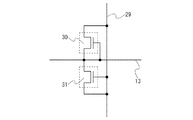
図2は保護回路の一例を示す。この保護回路は、走査線13と共通配線29の間に並列に配置された非線形素子30及び非線形素子31によって構成されている。非線形素子30及び非線形素子31は、ダイオードのような二端子素子又はトランジスタのような三端子素子で構成される。例えば、画素部の画素トランジスタと同じ工程で形成することも可能であり、例えばゲート端子とドレイン端子を接続することによりダイオードと同様の特性を持たせることができる。
FIG. 2 shows an example of a protection circuit. This protection circuit is composed of a
非線形素子30の第1端子(ゲート)と第3端子(ドレイン)は走査線13に接続され、第2端子(ソース)は共通配線29に接続されている。また、非線形素子31の第1端子(ゲート)と第3端子(ドレイン)は共通配線29に接続され、第2端子(ソース)は走査線13に接続されている。すなわち、図2で示す保護回路は、二つのトランジスタのそれぞれが、整流方向を互いに逆向きにして、走査線13と共通配線29を接続する構成である。言い換えると、走査線13と共通配線29の間に、整流方向が走査線13から共通配線29に向かうトランジスタと整流方向が共通配線29から走査線13に向かうトランジスタを接続する構成である。
The first terminal (gate) and the third terminal (drain) of the
図2で示す保護回路は、共通配線29に対し、走査線13が静電気等により正又は負に帯電した場合、その電荷を打ち消す方向に電流が流れる。例えば、走査線13が正に帯電した場合は、その正電荷を共通配線29に逃がす方向に電流が流れる。この動作により、帯電した走査線13に接続している画素トランジスタ19の静電破壊又はしきい値電圧のシフトを防止することができる。また、帯電している走査線13と絶縁層を介して交差する他の配線との間で、絶縁層の絶縁破壊を防止することができる。
In the protection circuit shown in FIG. 2, when the
なお、図2は走査線13に第1端子(ゲート)を接続した非線形素子30と、共通配線29に第1端子(ゲート)を接続した非線形素子31、すなわち整流方向が逆向きの二個一組の非線形素子を用い、それぞれの第2端子(ソース)と第3端子(ドレイン)で共通配線29と走査線13を並列に接続している。すなわち、非線形素子30と非線形素子31は並列である。他の構成として、さらに並列して接続する非線形素子を付加して、保護回路の動作安定性を高めても良い。例えば、図3は走査線13と共通配線29との間に設けられた、非線形素子30aと非線形素子30b及び非線形素子31aと非線形素子31bにより構成される保護回路を示す。この保護回路は、共通配線29に第1端子(ゲート)を接続した二つの非線形素子(30b、31b)と、走査線13に第1端子(ゲート)を接続した二つの非線形素子(30a、31a)の計四つの非線形素子を用いている。すなわち、整流方向が互いに逆向きになるよう2つの非線形素子を接続した一組を、共通配線29と走査線13の間に二組接続している。言い換えると、走査線13と共通配線29の間に、整流方向が走査線13から共通配線29に向かう2つのトランジスタと、整流方向が共通配線29から走査線13に向かう2つのトランジスタを接続する構成である。このように、共通配線29と走査線13を四つの非線形素子で接続することで、走査線13にサージ電圧が印加された場合のみならず、共通配線29静電気等により帯電した場合であっても、その電荷がそのまま走査線13に流れ込んでしまうのを防止することができる。なお、図9に、4つの非線形素子を基板上に配置する場合の一態様を等価回路図と共に示す。図9(B)に例示する等価回路図は図3と等価であり、図9(B)に記載されたそれぞれの非線形素子は図3に記載された非線形素子に対応する。具体的には、非線形素子740aは非線形素子30bに対応し、非線形素子740bは非線形素子31bに対応し、非線形素子740cは非線形素子30aに対応し、非線形素子740dは非線形素子31aに対応する。また、図9の走査線651は走査線13に対応し、共通配線650は共通配線29に対応する。従って、図9(A)に例示する4つの非線形素子を基板上に配置して形成した保護回路の一態様は、図3に例示する保護回路の一態様でもある。
2 shows the
また、奇数個の非線形素子を使った保護回路の例として、非線形素子の基板への配置例を図8(A)に、等価回路図を図8(B)に示す。この回路では非線形素子730cに対し、730b、730aがスイッチング素子として接続している。このように非線形素子を直列に接続することで、保護回路を構成する非線形素子に加わる瞬間的な負荷を分散できる。
As an example of a protection circuit using an odd number of nonlinear elements, FIG. 8A shows an example of arrangement of nonlinear elements on a substrate, and FIG. 8B shows an equivalent circuit diagram. In this circuit, 730b and 730a are connected as switching elements to the
図2は走査線13側に設ける保護回路の例を示すが、同様な構成の保護回路は信号線14側においても適用することができる。
Although FIG. 2 shows an example of a protection circuit provided on the
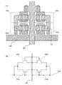
図4(A)は保護回路の一例を示す平面図であり、(B)はその等価回路図を示す。また、図4中に示されるQ1−Q2切断線に対応した断面図を図5に示す。以下の説明では図4及び図5を参照して保護回路の一構成例を説明する。 FIG. 4A is a plan view showing an example of a protection circuit, and FIG. 4B shows an equivalent circuit diagram thereof. FIG. 5 shows a cross-sectional view corresponding to the cutting line Q1-Q2 shown in FIG. In the following description, a configuration example of the protection circuit will be described with reference to FIGS.
非線形素子170a及び非線形素子170bは、走査線13と同じ層で形成されるゲート電極111及びゲート電極16を有している。ゲート電極111及びゲート電極16上にはゲート絶縁膜102が形成されている。ゲート絶縁膜102上には第1酸化物半導体層113が形成され、第1酸化物半導体層113のチャネル形成領域と重なる領域を覆ってチャネル保護層116が形成され、チャネル保護層116及び第1酸化物半導体層113を介してゲート電極111上で相対するように第1配線層117a及び第2配線層117bが設けられている。なお、非線形素子170a及び非線形素子170bは主要部において同じ構成を有している。
The
本発明の一態様ではゲート絶縁膜102に設けたコンタクトホール128を介して、ゲート電極111と同じ層で形成される走査線13と、非線形素子170aの第三端子(ドレイン)とを直接接続することで、接続に伴う界面の形成を一つに抑制できるだけでなく、接続に伴うコンタクトホールの形成を一つに抑制できる。
In one embodiment of the present invention, the
第1酸化物半導体層113は、相対する第1配線層117a及び第2配線層117bの下にゲート絶縁膜を介してゲート電極111を被覆するように設けられている。すなわち第1酸化物半導体層113は、チャネル形成領域と重なる領域を覆うチャネル保護層116の下面部と、ゲート電極111と重畳しゲート絶縁膜102の上面部と第2酸化物半導体層114aおよび114bの下面部とに、接するように設けられている。ここで、第1配線層117aは、第1酸化物半導体層113側から第2酸化物半導体層114aと導電層115aが積層された構成を有している。同様に、第2配線層117bは第1酸化物半導体層113側から第2酸化物半導体層114bと導電層115bが積層された構成を有している。
The first
第2酸化物半導体層(114a及び114b)は第1酸化物半導体層113と導電層(115a及び115b)に接してその間に設けられ、第1酸化物半導体層113と第1酸化物半導体層113よりも電気伝導率が高い第2酸化物半導体層(114aおよび114b)が接する、物性の異なる酸化物半導体層同士の接合が形成される。このような接合構造を非線形素子170a及び非線形素子170bに設けることにより、安定動作をさせることが可能となる。すなわち、熱的安定性が増し、安定動作をさせることが可能となる。それにより保護回路の機能を高め動作の安定化を図ることができる。また、接合リークが低減し、非線形素子170a及び非線形素子170bの特性を向上させることができる。
The second oxide semiconductor layers (114a and 114b) are provided in contact with and in contact with the first
本明細書中で第1酸化物半導体層に用いる酸化物半導体は、InMO3(ZnO)m(m>0)で表記される薄膜を形成し、その薄膜を半導体層として用いた非線形素子および薄膜トランジスタを作製する。なお、Mは、Ga、Fe、Ni、Mn及びCoから選ばれた一の金属元素又は複数の金属元素を示す。例えばMとして、Gaの場合があることの他、GaとNi又はGaとFeなど、Ga以外の上記金属元素が含まれる場合がある。また、上記酸化物半導体において、Mとして含まれる金属元素の他に、不純物元素としてFe、Niその他の遷移金属元素、又は該遷移金属の酸化物が含まれているものがある。本明細書においてはこの薄膜をIn−Ga−Zn−O系非単結晶膜とも呼ぶ。 The oxide semiconductor used for the first oxide semiconductor layer in this specification forms a thin film represented by InMO 3 (ZnO) m (m> 0), and a nonlinear element and a thin film transistor using the thin film as a semiconductor layer Is made. Note that M represents one metal element or a plurality of metal elements selected from Ga, Fe, Ni, Mn, and Co. For example, M may be Ga, and may contain the above metal elements other than Ga, such as Ga and Ni or Ga and Fe. In addition to the metal element contained as M, some of the above oxide semiconductors contain Fe, Ni, other transition metal elements, or oxides of the transition metal as impurity elements. In this specification, this thin film is also referred to as an In—Ga—Zn—O-based non-single-crystal film.
誘導結合プラズマ質量分析法(ICP−MS : Inductively Coupled Plasma Mass Spectrometry)により代表的な測定例を表1に示す。酸化インジウム(In2O3)と酸化ガリウム(Ga2O3)と酸化亜鉛(ZnO)の組成比を1:1:1(=In2O3:Ga2O3:ZnO)としたターゲット(In:Ga:Zn=1:1:0.5)を用い、スパッタ法でのアルゴンガス流量を40sccmとした条件1で得られる酸化物半導体膜は、InGa0.95Zn0.41O3.33である。また、スパッタ法でのアルゴンガス流量を10sccm、酸素を5sccmとした条件2で得られる酸化物半導体膜は、InGa0.94Zn0.40O3.31である。
Table 1 shows a typical measurement example by ICP-MS (Inductively Coupled Plasma Mass Spectrometry). A target in which the composition ratio of indium oxide (In 2 O 3 ), gallium oxide (Ga 2 O 3 ), and zinc oxide (ZnO) is 1: 1: 1 (= In 2 O 3 : Ga 2 O 3 : ZnO) In: Ga: Zn = 1: 1: 0.5), and the oxide semiconductor film obtained under the

また、測定方法をラザフォード後方散乱分析法(RBS : Rutherford Backscattering Spectrometry)に変えて定量化した結果を表2に示す。 Table 2 shows the results of quantification by changing the measurement method to Rutherford Backscattering Spectroscopy (RBS: Rutherford Backscattering Spectrometry).
条件1の試料をRBS分析で測定した結果、酸化物半導体膜は、InGa0.93Zn0.44O3.49である。また、条件2の試料をRBS分析で測定した結果、酸化物半導体膜は、InGa0.92Zn0.45O3.86である。
As a result of measuring the sample under
In−Ga−Zn−O系非単結晶膜の結晶構造は、アモルファス構造がX線回折(XRD:X−ray diffraction)の分析では観察される。なお、測定したサンプルのIn−Ga−Zn−O系非単結晶膜は、スパッタ法で成膜した後、加熱処理を200℃〜500℃、代表的には300〜400℃で10分〜100分行っている。また、薄膜トランジスタの電気特性もゲート電圧±20Vにおいて、オン・オフ比が109以上、移動度が10cm2/V・S以上のものを作製することができる。 As for the crystal structure of the In—Ga—Zn—O-based non-single-crystal film, an amorphous structure is observed by analysis of X-ray diffraction (XRD). Note that the measured In—Ga—Zn—O-based non-single-crystal film of the sample was formed by a sputtering method, and then heat treatment was performed at 200 to 500 ° C., typically 300 to 400 ° C. for 10 minutes to 100. Going minutes. In addition, as for the electrical characteristics of the thin film transistor, an on / off ratio of 10 9 or more and a mobility of 10 cm 2 / V · S or more can be manufactured at a gate voltage of ± 20 V.
第2酸化物半導体層(114aおよび114b)は、第1酸化物半導体層113よりも高い電気伝導率を有している。それゆえ、本実施の形態で例示する非線形素子170a及び非線形素子170bにおいて第2酸化物半導体層(114aおよび114b)は、トランジスタのソース領域及びドレイン領域と同様の機能を発現する。ソース領域及びドレイン領域となる第2の酸化物半導体層(114aおよび114b)は、n型の導電型を有し、活性化エネルギー(ΔE)が0.01eV以上0.1eV以下であり、n+領域とも呼べる。また、第2酸化物半導体層がIn、Ga、Zn、及びOを含む非単結晶酸化物半導体層である場合、非単結晶構造の中にナノクリスタルが含まれている場合がある。
The second oxide semiconductor layers (114a and 114b) have a higher electrical conductivity than the first
第1酸化物半導体層113のチャネル形成領域と重なる領域にはチャネル保護層116を設ける。従って、第1酸化物半導体層のゲート絶縁膜と接する面とは反対側の領域、所謂バックチャネルへダメージを与えることなく、第1配線層117a及び第2配線層117bを形成できる。
A channel
チャネル保護層116は、酸化シリコン又は酸化アルミニウムなどの酸化物で形成される。また、酸化シリコン又は酸化アルミニウム上に窒化シリコン、窒化アルミニウム、酸化窒化シリコン又は酸化窒化アルミニウムを積層することで、保護膜としてより機能を高めることができる。
The channel
いずれにしても、第1酸化物半導体層113と接するチャネル保護層116を酸化物とすることで、第1酸化物半導体層113から酸素が引き抜かれ、酸素欠乏型に変質してしまうことを防ぐことができる。また、第1酸化物半導体層113が窒化物による絶縁層と直接的に接しない構成とすることで、窒化物中の水素が拡散して第1酸化物半導体層113に水酸基などに起因する欠陥を生成するのを防ぐことができる。
In any case, by using the channel
このように、本実施の形態によれば、酸化物半導体により構成される保護回路を有する表示装置を得ることができる。第1酸化物半導体層よりも電気伝導率が高い第2酸化物半導体層を介して、導電層と第1酸化物半導体層が接合する領域を設けることで、安定動作をさせることが可能となる。それにより保護回路の機能を高め動作の安定化を図ることができる。また、ゲート絶縁膜102に設けたコンタクトホール128を介して、ゲート電極111と同じ層で形成される走査線13と、非線形素子170aの第三端子(ドレイン)とを直接接続することで、接続に伴う界面の形成を一つに抑制できるだけでなく、接続のためのコンタクトホールの形成を一つに抑制できる。その結果、保護回路の機能を高め動作の安定化を図ることができるだけでなく、保護回路の占有面積を小さくして、表示装置の小型化を図ることができる。特に、保護回路を構成する非線形素子が3つ、4つに増えるほど、接続に伴う界面の形成とコンタクトホールの形成を抑制する効果が大きくなる。また、チャネル保護層116を設けることで、バックチャネルへダメージを与えることなく、第1配線層117a及び第2配線層117bを形成できる。
Thus, according to this embodiment, a display device having a protection circuit formed using an oxide semiconductor can be obtained. By providing a region where the conductive layer and the first oxide semiconductor layer are joined via the second oxide semiconductor layer having higher electrical conductivity than the first oxide semiconductor layer, stable operation can be achieved. . Accordingly, the function of the protection circuit can be increased and the operation can be stabilized. Further, a connection is made by directly connecting the
なお、図4及び図5では走査線13に設けられる保護回路の一例を示すが、同様の保護回路を信号線、容量バス線などに適用することができる。
4 and 5 illustrate an example of a protection circuit provided in the
本実施の形態は、他の実施の形態に記載した構成と適宜組み合わせて実施することが可能である。 This embodiment can be implemented in appropriate combination with the structures described in the other embodiments.
(実施の形態2)
本実施の形態では、実施の形態1において図4(A)に示した保護回路の作製工程の一様態を図6乃至図7を参照して説明する。図6乃至図7は図4(A)中のQ1−Q2切断線に対応した断面図を表している。
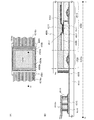
(Embodiment 2)
In this embodiment, one embodiment of a manufacturing process of the protection circuit illustrated in FIG. 4A in
図6(A)において、透光性を有する基板100には市販されているバリウムホウケイ酸ガラス、アルミノホウケイ酸ガラス及びアルミノシリケートガラスなどのガラス基板を用いることができる。例えば、成分比としてホウ酸(B2O3)よりも酸化バリウム(BaO)を多く含み、歪み点が730℃以上のガラス基板を用いると好ましい。酸化物半導体層を700℃程度の高温で熱処理する場合でも、ガラス基板が歪まないで済むからである。
6A, a glass substrate such as a commercially available barium borosilicate glass, aluminoborosilicate glass, or aluminosilicate glass can be used for the light-transmitting
次に、ゲート電極111および走査線13を含むゲート配線、容量配線および端子部の端子となる導電膜を基板100全面に成膜する。導電膜は、アルミニウム(Al)や銅(Cu)などの低抵抗導電性材料で形成することが望ましいが、Al単体では耐熱性が劣り、また腐蝕しやすい等の問題点があるので耐熱性導電性材料と組み合わせて形成する。耐熱性導電性材料としては、チタン(Ti)、タンタル(Ta)、タングステン(W)、モリブデン(Mo)、クロム(Cr)、Nd(ネオジム)、Sc(スカンジウム)から選ばれた元素、または上述した元素を成分とする合金か、または上述した元素を成分とする窒化物で形成する。
Next, a gate wiring including the
ゲート電極111となる導電膜は厚さ50nm以上300nm以下で形成する。ゲート電極111を含む配線層となる導電膜の厚さを300nm以下とすることで、後に形成される半導体膜や配線の段切れ防止が可能である。また、ゲート電極111を含む配線層となる導電膜の厚さを150nm以上とすることで、ゲート電極の抵抗を低減することが可能であり、大面積化が可能である。
The conductive film to be the
なお、ここでは基板100全面に導電膜としてアルミニウムを主成分とする膜とチタン膜をスパッタリング法により積層して成膜する。
Note that a film mainly composed of aluminum as a conductive film and a titanium film are stacked over the entire surface of the
次いで、本実施の形態における第1のフォトマスクを用いて形成したレジストマスクを使い、基板上に形成された導電膜の不要な部分をエッチングして除去して配線及び電極(ゲート電極111を含むゲート配線、容量配線、及び端子)を形成する。このとき少なくともゲート電極111の端部にテーパー形状が形成されるようにエッチングする。この段階での断面図を図6(A)に示す。
Next, unnecessary portions of the conductive film formed over the substrate are removed by etching using the resist mask formed using the first photomask in this embodiment to include wirings and electrodes (including the gate electrode 111) A gate wiring, a capacitor wiring, and a terminal). At this time, etching is performed so that at least an end portion of the
次にゲート絶縁膜102を形成する。ゲート絶縁膜102として利用できる絶縁膜としては、酸化珪素膜、窒化珪素膜、酸化窒化珪素膜、窒化酸化珪素膜、酸化アルミニウム膜、酸化マグネシウム膜、窒化アルミニウム膜、酸化イットリウム膜、酸化ハフニウム膜、酸化タンタル膜をその例に挙げることができる。
Next, the
ここでは、酸化窒化珪素膜とは、その組成として、窒素よりも酸素の含有量が多いものであって、濃度範囲として酸素が55〜65原子%、窒素が1〜20原子%、Siが25〜35原子%、水素が0.1〜10原子%の範囲で含まれるものをいう。また、窒化酸化珪素膜とは、その組成として、酸素よりも窒素の含有量が多いものであって、濃度範囲として酸素が15〜30原子%、窒素が20〜35原子%、Siが25〜35原子%、水素が15〜25原子%の範囲で含まれるものをいう。 Here, the silicon oxynitride film has a composition that contains more oxygen than nitrogen and has a concentration range of 55 to 65 atomic%, 1 to 20 atomic%, and 25 Si. -35 atomic%, and hydrogen is contained in the range of 0.1-10 atomic%. The silicon nitride oxide film has a composition containing more nitrogen than oxygen, and the concentration ranges of oxygen are 15 to 30 atomic%, nitrogen is 20 to 35 atomic%, and Si is 25 to 25%. 35 atomic% and hydrogen are included in the range of 15 to 25 atomic%.
ゲート絶縁膜は単層であっても、絶縁膜を2層または3層積層して形成してもよい。例えば、基板に接するゲート絶縁膜を窒化珪素膜、または窒化酸化珪素膜を用いて形成することで、基板とゲート絶縁膜の密着力が高まり、基板としてガラス基板を用いた場合、基板からの不純物が酸化物半導体層に拡散するのを防止することが可能であり、さらにゲート電極111を含む配線層の酸化を防止できる。即ち、膜剥れを防止することができると共に、後に形成される薄膜トランジスタの電気特性を向上させることができる。
The gate insulating film may be a single layer or may be formed by stacking two or three insulating films. For example, when a gate insulating film in contact with the substrate is formed using a silicon nitride film or a silicon nitride oxide film, adhesion between the substrate and the gate insulating film is increased, and when a glass substrate is used as the substrate, impurities from the substrate Can be prevented from diffusing into the oxide semiconductor layer, and oxidation of the wiring layer including the
また、ゲート絶縁膜102の厚さは50〜250nmとする。ゲート絶縁膜の厚さが50nm以上であると、ゲート電極111を含む配線層の凹凸を被覆できるため好ましい。ここでは、ゲート絶縁膜102としてプラズマCVD法またはスパッタリング法により100nmの厚みの酸化珪素膜を成膜する。
The thickness of the
次に、本実施の形態における第2のフォトマスクを用いて形成したレジストマスクにより、ゲート絶縁膜102をエッチングして、走査線13に達するコンタクトホール128を形成する。
Next, the
次に、第1酸化物半導体膜を形成する前のゲート絶縁膜102にプラズマ処理を行う。ここでは酸素ガスとアルゴンガスを導入してプラズマを発生させる逆スパッタを行い、露出しているゲート絶縁層に酸素ラジカル又は酸素を照射する。こうして、表面に付着しているゴミを除去する。
Next, plasma treatment is performed on the
なお、ゲート絶縁膜102のプラズマ処理、第1酸化物半導体膜、及びチャネル保護層となる絶縁膜は、スパッタ法で、チャンバーに導入するガスまたは設置するターゲットを適宣切り替えることにより大気に触れることなく連続成膜することができる。大気に触れることなく連続成膜すると、不純物の混入を防止することができる。大気に触れることなく連続成膜する場合、マルチチャンバー方式の製造装置を用いることが好ましい。
Note that the plasma treatment of the
特に、第1酸化物半導体膜に接するゲート絶縁膜102のプラズマ処理と第1酸化物半導体膜の成膜は大気に触れることなく連続で実施するのが望ましい。連続成膜することで、水蒸気などの大気成分や大気中に浮遊する不純物元素やゴミによる汚染がない積層界面を形成できるので、非線形素子および薄膜トランジスタの特性のばらつきを低減できる。
In particular, it is preferable that the plasma treatment of the
なお、本明細書中で連続成膜とは、スパッタ法で行う第1の処理工程からスパッタ法で行う第2の処理工程までの一連のプロセス中、被処理基板の置かれている雰囲気が大気等の汚染雰囲気に触れることなく、常に真空中または不活性ガス雰囲気(窒素雰囲気または希ガス雰囲気)で制御されていることを言う。連続成膜を行うことにより、清浄化された被処理基板に水分等が付着しないように保ちながら成膜を行うことができる。また、逆スパッタ処理のようなプラズマ処理も連続成膜に含むものとする。 Note that in this specification, continuous film formation refers to an atmosphere in which a substrate to be processed is placed in a series of processes from a first processing step performed by a sputtering method to a second processing step performed by a sputtering method. It means that it is always controlled in a vacuum or in an inert gas atmosphere (nitrogen atmosphere or rare gas atmosphere) without touching the contaminated atmosphere. By performing continuous film formation, film formation can be performed while keeping moisture or the like from adhering to the cleaned substrate to be processed. In addition, plasma treatment such as reverse sputtering treatment is included in the continuous film formation.
次いで、プラズマ処理されたゲート絶縁膜102を大気に曝すことなく第1酸化物半導体膜を成膜する。プラズマ処理されたゲート絶縁膜102を大気に曝すことなく第1酸化物半導体膜を成膜することにより、ゲート絶縁膜102と第1酸化物半導体膜の界面にゴミや水分が付着する不具合を防ぐことができる。なお、第1酸化物半導体膜の成膜は、先に逆スパッタを行ったチャンバーと同一チャンバーを用いてもよいし、大気に曝すことなく成膜できるのであれば、先に逆スパッタを行ったチャンバーと異なるチャンバーで成膜してもよい。
Next, a first oxide semiconductor film is formed without exposing the plasma-treated
ここでは、直径8インチのIn、Ga、及びZnを含む酸化物半導体ターゲット(組成比として、In2O3:Ga2O3:ZnO=1:1:1)を用いて、基板とターゲットの間との距離を170mm、圧力0.4Pa、直流(DC)電源0.5kW、アルゴン又は酸素雰囲気下で成膜する。なお、パルス直流(DC)電源を用いると、ごみが軽減でき、膜厚分布も均一となるために好ましい。第1酸化物半導体膜の膜厚は、5nm〜200nmとする。本実施の形態では第1酸化物半導体膜の膜厚は、100nmとする。 Here, an oxide semiconductor target containing 8 inches in diameter and containing In, Ga, and Zn (composition ratio: In 2 O 3 : Ga 2 O 3 : ZnO = 1: 1: 1) is used. The film is formed at a distance of 170 mm, a pressure of 0.4 Pa, a direct current (DC) power supply of 0.5 kW, and an argon or oxygen atmosphere. Note that a pulse direct current (DC) power source is preferable because dust can be reduced and the film thickness can be uniform. The thickness of the first oxide semiconductor film is 5 nm to 200 nm. In this embodiment, the thickness of the first oxide semiconductor film is 100 nm.
第2酸化物半導体膜より低い導電率を有する第1酸化物半導体膜は、第2酸化物半導体膜の成膜条件と異なる条件で成膜する。例えば、第2酸化物半導体膜の成膜条件における酸素ガス流量とアルゴンガス流量の比よりも第1酸化物半導体膜の成膜条件における酸素ガス流量の占める比率が多い条件とする。具体的には、第2酸化物半導体膜の成膜条件は、希ガス(アルゴン、又はヘリウムなど)雰囲気下(または酸素ガス10%以下、アルゴンガス90%以上)とし、第1酸化物半導体膜の成膜条件は、酸素雰囲気下(又は酸素ガス流量がアルゴンガス流量と等しいかそれ以上)とする。
The first oxide semiconductor film having lower conductivity than the second oxide semiconductor film is formed under conditions different from the film formation conditions of the second oxide semiconductor film. For example, the ratio of the oxygen gas flow rate in the film formation condition of the first oxide semiconductor film is larger than the ratio of the oxygen gas flow rate and the argon gas flow rate in the film formation condition of the second oxide semiconductor film. Specifically, the second oxide semiconductor film is formed under a rare gas (argon, helium, or the like) atmosphere (or
酸素を多く含む雰囲気で第1酸化物半導体膜を成膜することによって、第2酸化物半導体膜よりも導電率を低くすることができる。また、酸素を多く含む雰囲気で第1酸化物半導体膜を成膜することによって、オフ電流の低減を図ることができるため、オン・オフ比の高い薄膜トランジスタを得ることができる。 By forming the first oxide semiconductor film in an atmosphere containing a large amount of oxygen, the conductivity can be made lower than that of the second oxide semiconductor film. In addition, since the off-state current can be reduced by forming the first oxide semiconductor film in an oxygen-rich atmosphere, a thin film transistor with a high on / off ratio can be obtained.
次に、第1酸化物半導体膜上にチャネル保護層となる絶縁膜を、第1酸化物半導体膜の成膜に引き続いて連続成膜する。連続成膜することで、第1酸化物半導体膜のゲート絶縁膜と接する面とは反対側の領域、所謂バックチャネルに水蒸気などの大気成分や大気中に浮遊する不純物元素やゴミによる汚染がない積層界面を形成することができるので、非線形素子の特性のばらつきを低減できる。 Next, an insulating film serving as a channel protective layer is continuously formed on the first oxide semiconductor film following the formation of the first oxide semiconductor film. By continuously forming the film, the region opposite to the surface in contact with the gate insulating film of the first oxide semiconductor film, that is, the so-called back channel, is free from contamination by atmospheric components such as water vapor, impurity elements floating in the atmosphere, and dust. Since a laminated interface can be formed, variations in characteristics of nonlinear elements can be reduced.
なお、ここでは酸化珪素(人工石英)ターゲットと酸化物半導体膜用のターゲットを備えたマルチチャンバー型のスパッタリング装置を使って、前工程で形成した第1酸化物半導体膜を大気にさらすことなく、チャネル保護層として酸化珪素膜を成膜する。 Note that here, using a multi-chamber sputtering apparatus including a silicon oxide (artificial quartz) target and an oxide semiconductor film target, the first oxide semiconductor film formed in the previous step is not exposed to the atmosphere. A silicon oxide film is formed as a channel protective layer.
次に、本実施の形態における第3のフォトマスクを用いて形成したレジストマスクを使い、第1酸化物半導体膜上に形成された酸化珪素膜を選択的にエッチングしてチャネル保護層116を形成する。この段階での断面図を図6(B)に示す。
Next, the channel
次に、チャネル保護層116及び第1酸化物半導体膜上に第2酸化物半導体膜をスパッタ法で成膜する。ここでは、直径8インチのIn、Ga、及びZnを含む酸化物半導体ターゲット(組成比として、In2O3:Ga2O3:ZnO=1:1:1)を用いて、基板とターゲットの間との距離を170mm、圧力0.4Pa、直流(DC)電源0.5kW、成膜温度を室温とし、アルゴンガス流量40sccmを導入してスパッタ成膜を行う。これにより、第2酸化物半導体膜として、In、Ga、Zn及び酸素を成分とする半導体膜が形成される。In2O3:Ga2O3:ZnO=1:1:1としたターゲットを意図的に用いているにも関わらず、成膜直後で大きさ1nm〜10nmの結晶粒を含む酸化物半導体膜がしばしば形成される。なお、ターゲットの成分比、成膜圧力(0.1Pa〜2.0Pa)、電力(250W〜3000W:8インチφ)、温度(室温〜100℃)、反応性スパッタの成膜条件などを適宜調節することで結晶粒の有無や、結晶粒の密度や、直径サイズを、1nm〜10nmの範囲で調節されうると言える。第2酸化物半導体膜の膜厚は、5nm〜20nmとする。勿論、膜中に結晶粒が含まれる場合、含まれる結晶粒のサイズが膜厚を超える大きさとならない。本実施の形態では第2酸化物半導体膜の膜厚は、5nmとする。
Next, a second oxide semiconductor film is formed over the channel
次に、第4のフォトリソグラフィー工程を行い、レジストマスクを形成し、第1酸化物半導体膜および第2酸化物半導体膜をエッチングする。ここではITO07N(関東化学社製)を用いたウェットエッチングにより、不要な部分を除去して第1酸化物半導体層113および第2酸化物半導体層114を形成する。なお、ここでのエッチングは、ウェットエッチングに限定されずドライエッチングを用いてもよい。この段階での断面図を図6(C)に示す。
Next, a fourth photolithography step is performed to form a resist mask, and the first oxide semiconductor film and the second oxide semiconductor film are etched. Here, unnecessary portions are removed by wet etching using ITO07N (manufactured by Kanto Chemical Co., Inc.), and the first
次に、第2酸化物半導体層114およびゲート絶縁膜102上に金属材料からなる導電膜105をスパッタ法や真空蒸着法で形成する。導電膜105の材料としては、Al、Cr、Ta、Ti、Mo、Wから選ばれた元素、または上述した元素を成分とする合金か、上述した元素を組み合わせた合金膜等が挙げられる。
Next, a
また、工程中に200℃〜600℃の熱処理を行う場合には、この熱処理に耐える耐熱性を導電膜に持たせることが好ましい。Al単体では耐熱性が劣り、また腐蝕しやすい等の問題点があるので耐熱性導電性材料と組み合わせて形成する。Alと組み合わせる耐熱性導電性材料としては、チタン(Ti)、タンタル(Ta)、タングステン(W)、モリブデン(Mo)、クロム(Cr)、Nd(ネオジム)、Sc(スカンジウム)から選ばれた元素、または上述した元素を成分とする合金か、または上述した元素を成分とする窒化物で形成する。 Further, in the case where heat treatment at 200 ° C. to 600 ° C. is performed during the process, it is preferable that the conductive film has heat resistance that can withstand this heat treatment. Al alone is inferior in heat resistance and easily corroded, so it is formed in combination with a heat resistant conductive material. The heat-resistant conductive material combined with Al is an element selected from titanium (Ti), tantalum (Ta), tungsten (W), molybdenum (Mo), chromium (Cr), Nd (neodymium), and Sc (scandium). Or an alloy containing the above-described element as a component, or a nitride containing the above-described element as a component.
ここでは、導電膜105としてTi膜と、そのTi膜上に重ねてNdを含むアルミニウム(Al−Nd)膜を積層し、さらにその上にTi膜を成膜する3層構造とする。また、導電膜105は、2層構造としてもよく、アルミニウム膜上にチタン膜を積層してもよい。また、導電膜105は、シリコンを含むアルミニウム膜の単層構造や、チタン膜の単層構造としてもよい。この段階での断面図を図7(A)に示す。
Here, the
なお、ゲート絶縁膜102にはコンタクトホール128が形成されているため、成膜の際にソース電極層及びドレイン電極層となる導電膜105はコンタクトホール128を介して走査線13と接続する。
Note that since the
次に、第5のフォトリソグラフィー工程を行い、レジストマスク131を形成し、エッチングにより導電膜105の不要な部分を除去して導電層115a及び115bを形成する(図7(B)参照)。この際のエッチング方法としてウェットエッチングまたはドライエッチングを用いる。ここでは、SiCl4とCl2とBCl3の混合ガスを反応ガスとしたドライエッチングによりAl−Nd膜とTi膜を積層した導電膜をエッチングして導電層115a及び115bを形成する。この段階での断面図を図7(B)に示す。
Next, a fifth photolithography step is performed to form a resist
次いで、200℃〜600℃、代表的には300℃〜500℃の熱処理を行うことが好ましい。ここでは炉に入れ、窒素雰囲気下または大気雰囲気下で350℃、1時間の熱処理を行う。この熱処理によりIn−Ga−Zn−O系非単結晶膜の原子レベルの再配列が行われる。この熱処理によりキャリアの移動を阻害する歪が解放されるため、ここでの熱処理(光アニールも含む)は重要である。なお、熱処理を行うタイミングは、酸化物半導体膜の成膜後であれば特に限定されず、例えば画素電極形成後に行ってもよい。以上の工程で第1酸化物半導体層113をチャネル形成領域とする非線形素子170aが作製できる。
Next, it is preferable to perform heat treatment at 200 ° C. to 600 ° C., typically 300 ° C. to 500 ° C. Here, heat treatment is performed at 350 ° C. for one hour in a furnace in a nitrogen atmosphere or an air atmosphere. By this heat treatment, rearrangement at the atomic level of the In—Ga—Zn—O-based non-single-crystal film is performed. Since heat treatment releases strain that hinders carrier movement, heat treatment here (including optical annealing) is important. Note that the timing for performing the heat treatment is not particularly limited as long as it is after the formation of the oxide semiconductor film, and for example, it may be performed after the pixel electrode is formed. Through the above process, the
次いで、非線形素子170aを覆う層間絶縁膜107を形成する。層間絶縁膜107はスパッタ法などを用いて得られる窒化シリコン膜、酸化シリコン膜、酸化窒化シリコン膜、酸化アルミニウム膜、酸化タンタル膜などを用いることができる。こうして5回のフォトリソグラフィー工程により、5枚のフォトマスクを使用して、複数の非線形素子を有する(本実施の形態では、170aおよび170bの二つの非線形素子を有する)保護回路を完成させることができる。この段階での断面図を図7(C)に示す。
Next, an
保護回路の形成に引き続き、非線形素子と同一のプロセスで一体形成した表示装置の画素部分の薄膜トランジスタに、画素電極を形成する。なお、画素部分の薄膜トランジスタは図示していない。先ず、図示していない第6のレジストマスクを用いて、やはり図示していない画素部分の薄膜トランジスタのドレイン電極層に達するコンタクトホールを層間絶縁膜107に形成する。
Subsequent to the formation of the protective circuit, a pixel electrode is formed on the thin film transistor in the pixel portion of the display device integrally formed by the same process as the nonlinear element. Note that the thin film transistor in the pixel portion is not shown. First, a contact hole reaching the drain electrode layer of the thin film transistor in the pixel portion (not shown) is formed in the
次いで、レジストマスクを除去した後、透明導電膜を成膜する。透明導電膜の材料としては、酸化インジウム(In2O3)や酸化インジウム酸化スズ合金(In2O3―SnO2、ITOと略記する)などをスパッタ法や真空蒸着法などを用いて形成する。このような材料のエッチング処理は塩酸系の溶液により行う。しかし、特にITOのエッチングは残渣が発生しやすいので、エッチング加工性を改善するために酸化インジウム酸化亜鉛合金(In2O3―ZnO)を用いても良い。 Next, after removing the resist mask, a transparent conductive film is formed. As a material for the transparent conductive film, indium oxide (In 2 O 3 ), an indium tin oxide alloy (In 2 O 3 —SnO 2 , abbreviated as ITO), or the like is formed by a sputtering method, a vacuum evaporation method, or the like. . Etching treatment of such a material is performed with a hydrochloric acid based solution. However, in particular, since etching of ITO is likely to generate a residue, an indium oxide-zinc oxide alloy (In 2 O 3 —ZnO) may be used to improve etching processability.
次に、第7のフォトリソグラフィー工程を行い、レジストマスクを形成し、エッチングにより透明導電膜の不要な部分を除去して画素電極を形成する。また、容量部におけるゲート絶縁膜102及び層間絶縁膜107を誘電体として、容量配線と画素電極とで保持容量を形成する。また、端子部に透明導電膜を残し、FPCとの接続に用いる電極または配線や、ソース配線の入力端子として機能する接続用の端子電極を形成する。
Next, a seventh photolithography step is performed to form a resist mask, and unnecessary portions of the transparent conductive film are removed by etching to form pixel electrodes. In addition, a storage capacitor is formed by the capacitor wiring and the pixel electrode using the
こうして、非線形素子と同一のプロセスで一体形成した複数の薄膜トランジスタに画素電極を形成すると、nチャネル型TFTを有する画素部の作製と保護回路の作製を同時におこなうことができる。第1酸化物半導体層よりも電気伝導率が高い第2酸化物半導体層と接合する領域を設けることで、安定動作をさせることが可能となる。それにより保護回路の機能を高め動作の安定化を図ることができる。また、ゲート絶縁膜102に設けたコンタクトホール128を介して、ゲート電極111と同じ層で形成される走査線13と、非線形素子170aの第三端子(ドレイン)とを直接接続することで、接続に伴う界面の形成を一つに抑制できるだけでなく、接続のためのコンタクトホールの形成を一つに抑制できる。その結果、保護回路の機能を高め動作の安定化を図ることができるだけでなく、保護回路の占有面積を小さくして、表示装置の小型化を図ることができる。すなわち、本実施の形態に示した工程に従えば、保護回路の機能を高め動作の安定化を図ることができるだけでなく、占有面積が小さい保護回路を搭載したアクティブマトリクス型の表示装置用基板を作製できる。また、チャネル保護層116を設けることで、バックチャネルへダメージを与えることなく、第1配線層117a及び第2配線層117bを形成できる。
In this manner, when a pixel electrode is formed on a plurality of thin film transistors integrally formed by the same process as the nonlinear element, a pixel portion having an n-channel TFT and a protection circuit can be manufactured at the same time. Providing a region to be joined to the second oxide semiconductor layer having higher electrical conductivity than the first oxide semiconductor layer makes it possible to perform stable operation. Accordingly, the function of the protection circuit can be increased and the operation can be stabilized. Further, a connection is made by directly connecting the
本実施の形態は、他の実施の形態に記載した構成と適宜組み合わせて実施することが可能である。 This embodiment can be implemented in appropriate combination with the structures described in the other embodiments.
(実施の形態3)
本実施の形態では、本発明の一態様を適用した表示装置として同一基板上に保護回路と、画素部に配置する薄膜トランジスタを有する電子ペーパーの例を示す。
(Embodiment 3)
In this embodiment, an example of electronic paper including a protective circuit and a thin film transistor provided in a pixel portion over the same substrate as a display device to which one embodiment of the present invention is applied is described.
図10は、本発明の一態様を適用した表示装置の例としてアクティブマトリクス型の電子ペーパーを示す。半導体装置に用いられる薄膜トランジスタ581としては、実施の形態2で示す非線形素子と同様に作製でき、In、Ga、及びZnを含む酸化物半導体を半導体層に用いた電気特性の高い薄膜トランジスタである。
FIG. 10 illustrates active matrix electronic paper as an example of a display device to which one embodiment of the present invention is applied. The
図10の電子ペーパーは、ツイストボール表示方式を用いた表示装置の例である。ツイストボール表示方式とは、白と黒に塗り分けられた球形粒子を表示素子に用い、電極層である第1の電極層及び第2の電極層の間に配置し、第1の電極層及び第2の電極層に電位差を生じさせての球形粒子の向きを制御することにより、表示を行う方法である。 The electronic paper in FIG. 10 is an example of a display device using a twisting ball display system. The twist ball display method uses spherical particles that are painted in white and black as a display element, and is arranged between the first electrode layer and the second electrode layer, which are electrode layers, In this method, display is performed by controlling the orientation of the spherical particles by generating a potential difference in the second electrode layer.
基板580上に形成された薄膜トランジスタ581は、ゲート絶縁層583と絶縁層584を有するボトムゲート構造の薄膜トランジスタであり、絶縁層585に形成する開口を介して、ソース電極層又はドレイン電極層が第1の電極層587と電気的に接続している。第1の電極層587と基板596に形成された第2の電極層588との間には黒色領域590a及び白色領域590bを有し、周りに液体で満たされているキャビティ594を含む球形粒子589が設けられており、球形粒子589の周囲は樹脂等の充填材595で充填されている(図10参照。)。
The
また、ツイストボールの代わりに、電気泳動素子を用いることも可能である。透明な液体と、正に帯電した白い微粒子と負に帯電した黒い微粒子とを封入した直径10μm〜200μm程度のマイクロカプセルを用いる。第1の電極層と第2の電極層との間に設けられるマイクロカプセルは、第1の電極層と第2の電極層によって、電場が与えられると、白い微粒子と、黒い微粒子が逆の方向に移動し、白または黒を表示することができる。この原理を応用した表示素子が電気泳動表示素子であり、一般的に電子ペーパーとよばれている。電気泳動表示素子は、液晶表示素子に比べて反射率が高いため、補助ライトは不要であり、また消費電力が小さく、薄暗い場所でも表示部を認識することが可能である。また、表示部に電源が供給されない場合であっても、一度表示した像を保持することが可能である。従って、例えば電源供給源となる電波発信源から表示機能付き半導体装置(単に表示装置、又は表示装置を具備する半導体装置ともいう)を遠ざけた場合であっても、表示された像を保存しておくことが可能となる。 Further, instead of the twisting ball, an electrophoretic element can be used. A microcapsule having a diameter of about 10 μm to 200 μm in which transparent liquid, positively charged white microparticles, and negatively charged black microparticles are enclosed is used. In the microcapsule provided between the first electrode layer and the second electrode layer, when an electric field is applied by the first electrode layer and the second electrode layer, the white particles and the black particles are in opposite directions. And can display white or black. A display element using this principle is an electrophoretic display element, and is generally called electronic paper. Since the electrophoretic display element has higher reflectance than the liquid crystal display element, an auxiliary light is unnecessary, power consumption is small, and the display portion can be recognized even in a dim place. Further, even when power is not supplied to the display portion, an image once displayed can be held. Therefore, for example, even when a semiconductor device with a display function (also simply referred to as a display device or a semiconductor device including a display device) is moved away from a radio wave source serving as a power supply source, the displayed image is stored. It becomes possible to leave.
以上の工程により作製した電子ペーパーが搭載している保護回路は、接続のためのコンタクトホールを減らして占有面積を減らしているうえ、第1酸化物半導体層よりも電気伝導率が高い第2酸化物半導体層を第1酸化物半導体層と配線層の間に設けられており、機能が高く、動作が安定している。従って、このような保護回路を搭載した本実施の形態の電子ペーパーは、信頼性が高い。 The protection circuit mounted on the electronic paper manufactured through the above steps reduces the contact hole for connection to reduce the occupied area, and the second oxide has higher electrical conductivity than the first oxide semiconductor layer. The physical semiconductor layer is provided between the first oxide semiconductor layer and the wiring layer, and has high function and stable operation. Therefore, the electronic paper of this embodiment equipped with such a protection circuit has high reliability.
本実施の形態は、他の実施の形態に記載した構成と適宜組み合わせて実施することが可能である。 This embodiment can be implemented in appropriate combination with the structures described in the other embodiments.
(実施の形態4)
本実施の形態では、本発明の一態様である表示装置において、同一基板上に少なくとも保護回路と、駆動回路の一部と、画素部に配置する薄膜トランジスタを作製する例について図11乃至図16を用いて以下に説明する。
(Embodiment 4)
In this embodiment, FIGS. 11 to 16 illustrate an example of manufacturing at least a protective circuit, part of a driver circuit, and a thin film transistor provided in a pixel portion over the same substrate in the display device which is one embodiment of the present invention. This will be described below.
保護回路と同一基板上の画素部に配置する薄膜トランジスタは、実施の形態2で示す非線形素子と同様に形成する。また、形成した薄膜トランジスタはnチャネル型TFTであるため、駆動回路のうち、nチャネル型TFTで構成することができる駆動回路の一部を画素部の薄膜トランジスタと同一基板上に形成する。
A thin film transistor disposed in a pixel portion over the same substrate as the protective circuit is formed in a manner similar to the nonlinear element described in
本発明の一態様であるアクティブマトリクス型液晶表示装置のブロック図の一例を図11(A)に示す。図11(A)に示す表示装置は、基板5300上に表示素子を備えた画素を複数有する画素部5301と、各画素を選択する走査線駆動回路5302と、選択された画素へのビデオ信号の入力を制御する信号線駆動回路5303とを有する。
FIG. 11A illustrates an example of a block diagram of an active matrix liquid crystal display device which is one embodiment of the present invention. A display device illustrated in FIG. 11A includes a pixel portion 5301 having a plurality of pixels each provided with a display element over a
画素部5301は、信号線駆動回路5303から列方向に伸張して配置された複数の信号線S1〜Sm(図示せず。)により信号線駆動回路5303と接続され、走査線駆動回路5302から行方向に伸張して配置された複数の走査線G1〜Gn(図示せず。)により走査線駆動回路5302と接続され、信号線S1〜Sm並びに走査線G1〜Gnに対応してマトリクス状に配置された複数の画素(図示せず。)を有する。そして、各画素は、信号線Sj(信号線S1〜Smのうちいずれか一)、走査線Gi(走査線G1〜Gnのうちいずれか一)と接続される。
The pixel portion 5301 is connected to the signal line driver circuit 5303 by a plurality of signal lines S1 to Sm (not shown) arranged extending from the signal line driver circuit 5303 in the column direction. A plurality of scanning lines G1 to Gn (not shown) arranged in the direction are connected to the scanning
また、実施の形態2で示す非線形素子と共に同様の方法で形成できる薄膜トランジスタは、nチャネル型TFTであり、nチャネル型TFTで構成する信号線駆動回路について図12を用いて説明する。
A thin film transistor which can be formed by the same method as the nonlinear element described in
図12に示す信号線駆動回路は、ドライバIC5601、スイッチ群5602_1〜5602_M、第1の配線5611、第2の配線5612、第3の配線5613及び配線5621_1〜5621_Mを有する。スイッチ群5602_1〜5602_Mそれぞれは、第1の薄膜トランジスタ5603a、第2の薄膜トランジスタ5603b及び第3の薄膜トランジスタ5603cを有する。
The signal line driver circuit illustrated in FIG. 12 includes a
ドライバIC5601は第1の配線5611、第2の配線5612、第3の配線5613及び配線5621_1〜5621_Mに接続される。そして、スイッチ群5602_1〜5602_Mそれぞれは、第1の配線5611、第2の配線5612、第3の配線5613及びスイッチ群5602_1〜5602_Mそれぞれに対応した配線5621_1〜5621_Mに接続される。そして、配線5621_1〜5621_Mそれぞれは、第1の薄膜トランジスタ5603a、第2の薄膜トランジスタ5603b及び第3の薄膜トランジスタ5603cを介して、3つの信号線に接続される。例えば、J列目の配線5621_J(配線5621_1〜配線5621_Mのうちいずれか一)は、スイッチ群5602_Jが有する第1の薄膜トランジスタ5603a、第2の薄膜トランジスタ5603b及び第3の薄膜トランジスタ5603cを介して、信号線Sj−1、信号線Sj、信号線Sj+1に接続される。
The
なお、第1の配線5611、第2の配線5612、第3の配線5613には、それぞれ信号が入力される。
Note that a signal is input to each of the
なお、ドライバIC5601は、単結晶基板上に形成されていることが望ましい。さらに、スイッチ群5602_1〜5602_Mは、画素部と同一基板上に形成されていることが望ましい。したがって、ドライバIC5601とスイッチ群5602_1〜5602_MとはFPCなどを介して接続するとよい。
Note that the
次に、図12に示した信号線駆動回路の動作について、図13のタイミングチャートを参照して説明する。なお、図13のタイミングチャートは、i行目の走査線Giが選択されている場合のタイミングチャートを示している。さらに、i行目の走査線Giの選択期間は、第1のサブ選択期間T1、第2のサブ選択期間T2及び第3のサブ選択期間T3に分割されている。さらに、図12の信号線駆動回路は、他の行の走査線が選択されている場合でも図13と同様の動作をする。 Next, operation of the signal line driver circuit illustrated in FIG. 12 is described with reference to a timing chart in FIG. The timing chart of FIG. 13 shows the timing chart when the i-th scanning line Gi is selected. Further, the selection period of the i-th scanning line Gi is divided into a first sub-selection period T1, a second sub-selection period T2, and a third sub-selection period T3. Further, the signal line driver circuit in FIG. 12 operates in the same manner as in FIG. 13 even when a scan line in another row is selected.
なお、図13のタイミングチャートは、J列目の配線5621_Jが第1の薄膜トランジスタ5603a、第2の薄膜トランジスタ5603b及び第3の薄膜トランジスタ5603cを介して、信号線Sj−1、信号線Sj、信号線Sj+1に接続される場合について示している。
Note that in the timing chart of FIG. 13, the wiring 5621_J in the J-th column is connected to the signal line Sj−1, the signal line Sj, and the signal line Sj + 1 through the first
なお、図13のタイミングチャートは、i行目の走査線Giが選択されるタイミング、第1の薄膜トランジスタ5603aのオン・オフのタイミング5703a、第2の薄膜トランジスタ5603bのオン・オフのタイミング5703b、第3の薄膜トランジスタ5603cのオン・オフのタイミング5703c及びJ列目の配線5621_Jに入力される信号5721_Jを示している。
Note that the timing chart in FIG. 13 illustrates the timing at which the i-th scanning line Gi is selected, the on / off timing 5703a of the first
なお、配線5621_1〜配線5621_Mには第1のサブ選択期間T1、第2のサブ選択期間T2及び第3のサブ選択期間T3において、それぞれ別のビデオ信号が入力される。例えば、第1のサブ選択期間T1において配線5621_Jに入力されるビデオ信号は信号線Sj−1に入力され、第2のサブ選択期間T2において配線5621_Jに入力されるビデオ信号は信号線Sjに入力され、第3のサブ選択期間T3において配線5621_Jに入力されるビデオ信号は信号線Sj+1に入力される。さらに、第1のサブ選択期間T1、第2のサブ選択期間T2及び第3のサブ選択期間T3において、配線5621_Jに入力されるビデオ信号をそれぞれData_j−1、Data_j、Data_j+1とする。
Note that different video signals are input to the wirings 5621_1 to 5621_M in the first sub-selection period T1, the second sub-selection period T2, and the third sub-selection period T3. For example, a video signal input to the wiring 5621_J in the first sub-selection period T1 is input to the signal line Sj-1, and a video signal input to the wiring 5621_J in the second sub-selection period T2 is input to the signal line Sj. Then, the video signal input to the wiring 5621_J in the third sub-selection period T3 is input to the signal
図13に示すように、第1のサブ選択期間T1において第1の薄膜トランジスタ5603aがオンし、第2の薄膜トランジスタ5603b及び第3の薄膜トランジスタ5603cがオフする。このとき、配線5621_Jに入力されるData_j−1が、第1の薄膜トランジスタ5603aを介して信号線Sj−1に入力される。第2のサブ選択期間T2では、第2の薄膜トランジスタ5603bがオンし、第1の薄膜トランジスタ5603a及び第3の薄膜トランジスタ5603cがオフする。このとき、配線5621_Jに入力されるData_jが、第2の薄膜トランジスタ5603bを介して信号線Sjに入力される。第3のサブ選択期間T3では、第3の薄膜トランジスタ5603cがオンし、第1の薄膜トランジスタ5603a及び第2の薄膜トランジスタ5603bがオフする。このとき、配線5621_Jに入力されるData_j+1が、第3の薄膜トランジスタ5603cを介して信号線Sj+1に入力される。
As shown in FIG. 13, in the first sub-selection period T1, the first
以上のことから、図12の信号線駆動回路は、1ゲート選択期間を3つに分割することで、1ゲート選択期間中に1つの配線5621から3つの信号線にビデオ信号を入力することができる。したがって、図12の信号線駆動回路は、ドライバIC5601が形成される基板と、画素部が形成されている基板との接続数を信号線の数に比べて約1/3にすることができる。接続数が約1/3になることによって、図12の信号線駆動回路は、信頼性、歩留まりなどを向上できる。
From the above, the signal line driver circuit in FIG. 12 can input a video signal from one wiring 5621 to three signal lines during one gate selection period by dividing one gate selection period into three. it can. Therefore, the signal line driver circuit in FIG. 12 can reduce the number of connections between the substrate on which the
なお、図12のように、1ゲート選択期間を複数のサブ選択期間に分割し、複数のサブ選択期間それぞれにおいて、ある1つの配線から複数の信号線それぞれにビデオ信号を入力することができれば、薄膜トランジスタの配置や数、駆動方法などは限定されない。 Note that as shown in FIG. 12, if one gate selection period is divided into a plurality of sub-selection periods, and a video signal can be input from a certain wiring to each of a plurality of signal lines in each of the plurality of sub-selection periods, The arrangement and number of thin film transistors and the driving method are not limited.
例えば、3つ以上のサブ選択期間それぞれにおいて1つの配線から3つ以上の信号線それぞれにビデオ信号を入力する場合は、薄膜トランジスタ及び薄膜トランジスタを制御するための配線を追加すればよい。ただし、1ゲート選択期間を4つ以上のサブ選択期間に分割すると、1つのサブ選択期間が短くなる。したがって、1ゲート選択期間は、2つ又は3つのサブ選択期間に分割されることが望ましい。 For example, when video signals are input from one wiring to each of three or more signal lines in each of three or more sub-selection periods, a thin film transistor and a wiring for controlling the thin film transistor may be added. However, if one gate selection period is divided into four or more sub selection periods, one sub selection period is shortened. Therefore, it is desirable that one gate selection period is divided into two or three sub selection periods.
別の例として、図14のタイミングチャートに示すように、1つの選択期間をプリチャージ期間Tp、第1のサブ選択期間T1、第2のサブ選択期間T2、第3のサブ選択期間T3に分割してもよい。さらに、図14のタイミングチャートは、i行目の走査線Giが選択されるタイミング、第1の薄膜トランジスタ5603aのオン・オフのタイミング5803a、第2の薄膜トランジスタ5603bのオン・オフのタイミング5803b、第3の薄膜トランジスタ5603cのオン・オフのタイミング5803c及びJ列目の配線5621_Jに入力される信号5821_Jを示している。図14に示すように、プリチャージ期間Tpにおいて第1の薄膜トランジスタ5603a、第2の薄膜トランジスタ5603b及び第3の薄膜トランジスタ5603cがオンする。このとき、配線5621_Jに入力されるプリチャージ電圧Vpが第1の薄膜トランジスタ5603a、第2の薄膜トランジスタ5603b及び第3の薄膜トランジスタ5603cを介してそれぞれ信号線Sj−1、信号線Sj、信号線Sj+1に入力される。第1のサブ選択期間T1において第1の薄膜トランジスタ5603aがオンし、第2の薄膜トランジスタ5603b及び第3の薄膜トランジスタ5603cがオフする。このとき、配線5621_Jに入力されるData_j−1が、第1の薄膜トランジスタ5603aを介して信号線Sj−1に入力される。第2のサブ選択期間T2では、第2の薄膜トランジスタ5603bがオンし、第1の薄膜トランジスタ5603a及び第3の薄膜トランジスタ5603cがオフする。このとき、配線5621_Jに入力されるData_jが、第2の薄膜トランジスタ5603bを介して信号線Sjに入力される。第3のサブ選択期間T3では、第3の薄膜トランジスタ5603cがオンし、第1の薄膜トランジスタ5603a及び第2の薄膜トランジスタ5603bがオフする。このとき、配線5621_Jに入力されるData_j+1が、第3の薄膜トランジスタ5603cを介して信号線Sj+1に入力される。
As another example, as shown in the timing chart of FIG. 14, one selection period is divided into a precharge period Tp, a first sub-selection period T1, a second sub-selection period T2, and a third sub-selection period T3. May be. Further, in the timing chart of FIG. 14, the timing at which the i-th scanning line Gi is selected, the on / off timing 5803a of the first
以上のことから、図14のタイミングチャートを適用した図12の信号線駆動回路は、サブ選択期間の前にプリチャージ選択期間を設けることによって、信号線をプリチャージできるため、画素へのビデオ信号の書き込みを高速に行うことができる。なお、図14において、図13と同様なものに関しては共通の符号を用いて示し、同一部分又は同様な機能を有する部分の詳細な説明は省略する。 From the above, the signal line driver circuit in FIG. 12 to which the timing chart in FIG. 14 is applied can precharge the signal line by providing the precharge selection period before the sub selection period. Can be written at high speed. Note that in FIG. 14, components similar to those in FIG. 13 are denoted by common reference numerals, and detailed description of the same portions or portions having similar functions is omitted.
また、走査線駆動回路の構成について説明する。走査線駆動回路は、シフトレジスタ、バッファを有している。また場合によってはレベルシフタを有していても良い。走査線駆動回路において、シフトレジスタにクロック信号(CLK)及びスタートパルス信号(SP)が入力されることによって、選択信号が生成される。生成された選択信号はバッファにおいて緩衝増幅され、対応する走査線に供給される。走査線には、1ライン分の画素のトランジスタのゲート電極が接続されている。そして、1ライン分の画素のトランジスタを一斉にONにしなくてはならないので、バッファは大きな電流を流すことが可能なものが用いられる。 A structure of the scan line driver circuit will be described. The scan line driver circuit includes a shift register and a buffer. In some cases, a level shifter may be provided. In the scan line driver circuit, when a clock signal (CLK) and a start pulse signal (SP) are input to the shift register, a selection signal is generated. The generated selection signal is buffered and amplified in the buffer and supplied to the corresponding scanning line. A gate electrode of a transistor of a pixel for one line is connected to the scanning line. Since the transistors of pixels for one line must be turned on all at once, a buffer that can flow a large current is used.
走査線駆動回路の一部に用いるシフトレジスタの一形態について図15及び図16を用いて説明する。 One mode of a shift register used for part of the scan line driver circuit is described with reference to FIGS.
図15にシフトレジスタの回路構成を示す。図15に示すシフトレジスタは、フリップフロップ5701_1〜5701_nという複数のフリップフロップで構成される。また、第1のクロック信号、第2のクロック信号、スタートパルス信号、リセット信号が入力されて動作する。 FIG. 15 shows a circuit configuration of the shift register. The shift register illustrated in FIG. 15 includes a plurality of flip-flops, flip-flops 5701_1 to 5701_n. In addition, the first clock signal, the second clock signal, the start pulse signal, and the reset signal are input to operate.
図15のシフトレジスタの接続関係について説明する。図15のシフトレジスタは、i段目のフリップフロップ5701_i(フリップフロップ5701_1〜5701_nのうちいずれか一)は、図16に示した第1の配線5501が第7の配線5717_i−1に接続され、図16に示した第2の配線5502が第7の配線5717_i+1に接続され、図16に示した第3の配線5503が第7の配線5717_iに接続され、図16に示した第6の配線5506が第5の配線5715に接続される。
Connection relations of the shift register in FIG. 15 are described. In the shift register in FIG. 15, the i-th flip-flop 5701_i (any one of the flip-flops 5701_1 to 5701_n) has the
また、図16に示した第4の配線5504が奇数段目のフリップフロップでは第2の配線5712に接続され、偶数段目のフリップフロップでは第3の配線5713に接続され、図16に示した第5の配線5505が第4の配線5714に接続される。
The
ただし、1段目のフリップフロップ5701_1の図16に示す第1の配線5501は第1の配線5711に接続され、n段目のフリップフロップ5701_nの図16に示す第2の配線5502は第6の配線5716に接続される。
Note that the
なお、第1の配線5711、第2の配線5712、第3の配線5713、第6の配線5716を、それぞれ第1の信号線、第2の信号線、第3の信号線、第4の信号線と呼んでもよい。さらに、第4の配線5714、第5の配線5715を、それぞれ第1の電源線、第2の電源線と呼んでもよい。
Note that the
次に、図15に示すフリップフロップの詳細について、図16に示す。図16に示すフリップフロップは、第1の薄膜トランジスタ5571、第2の薄膜トランジスタ5572、第3の薄膜トランジスタ5573、第4の薄膜トランジスタ5574、第5の薄膜トランジスタ5575、第6の薄膜トランジスタ5576、第7の薄膜トランジスタ5577及び第8の薄膜トランジスタ5578を有する。なお、第1の薄膜トランジスタ5571、第2の薄膜トランジスタ5572、第3の薄膜トランジスタ5573、第4の薄膜トランジスタ5574、第5の薄膜トランジスタ5575、第6の薄膜トランジスタ5576、第7の薄膜トランジスタ5577及び第8の薄膜トランジスタ5578は、nチャネル型トランジスタであり、ゲート・ソース間電圧(Vgs)がしきい値電圧(Vth)を上回ったとき導通状態になるものとする。
Next, FIG. 16 shows details of the flip-flop shown in FIG. 16 includes a first
次に、図16に示すフリップフロップの接続構成について、以下に示す。 Next, a connection structure of the flip-flop illustrated in FIG. 16 is described below.
第1の薄膜トランジスタ5571の第1の電極(ソース電極またはドレイン電極の一方)が第4の配線5504に接続され、第1の薄膜トランジスタ5571の第2の電極(ソース電極またはドレイン電極の他方)が第3の配線5503に接続される。
A first electrode (one of a source electrode and a drain electrode) of the first
第2の薄膜トランジスタ5572の第1の電極が第6の配線5506に接続され、第2の薄膜トランジスタ5572第2の電極が第3の配線5503に接続される。
A first electrode of the second
第3の薄膜トランジスタ5573の第1の電極が第5の配線5505に接続され、第3の薄膜トランジスタ5573の第2の電極が第2の薄膜トランジスタ5572のゲート電極に接続され、第3の薄膜トランジスタ5573のゲート電極が第5の配線5505に接続される。
The first electrode of the third
第4の薄膜トランジスタ5574の第1の電極が第6の配線5506に接続され、第4の薄膜トランジスタ5574の第2の電極が第2の薄膜トランジスタ5572のゲート電極に接続され、第4の薄膜トランジスタ5574のゲート電極が第1の薄膜トランジスタ5571のゲート電極に接続される。
The first electrode of the fourth
第5の薄膜トランジスタ5575の第1の電極が第5の配線5505に接続され、第5の薄膜トランジスタ5575の第2の電極が第1の薄膜トランジスタ5571のゲート電極に接続され、第5の薄膜トランジスタ5575のゲート電極が第1の配線5501に接続される。
The first electrode of the fifth
第6の薄膜トランジスタ5576の第1の電極が第6の配線5506に接続され、第6の薄膜トランジスタ5576の第2の電極が第1の薄膜トランジスタ5571のゲート電極に接続され、第6の薄膜トランジスタ5576のゲート電極が第2の薄膜トランジスタ5572のゲート電極に接続される。
The first electrode of the sixth
第7の薄膜トランジスタ5577の第1の電極が第6の配線5506に接続され、第7の薄膜トランジスタ5577の第2の電極が第1の薄膜トランジスタ5571のゲート電極に接続され、第7の薄膜トランジスタ5577のゲート電極が第2の配線5502に接続される。第8の薄膜トランジスタ5578の第1の電極が第6の配線5506に接続され、第8の薄膜トランジスタ5578の第2の電極が第2の薄膜トランジスタ5572のゲート電極に接続され、第8の薄膜トランジスタ5578のゲート電極が第1の配線5501に接続される。
The first electrode of the seventh
なお、第1の薄膜トランジスタ5571のゲート電極、第4の薄膜トランジスタ5574のゲート電極、第5の薄膜トランジスタ5575の第2の電極、第6の薄膜トランジスタ5576の第2の電極及び第7の薄膜トランジスタ5577の第2の電極の接続箇所をノード5543とする。さらに、第2の薄膜トランジスタ5572のゲート電極、第3の薄膜トランジスタ5573の第2の電極、第4の薄膜トランジスタ5574の第2の電極、第6の薄膜トランジスタ5576のゲート電極及び第8の薄膜トランジスタ5578の第2の電極の接続箇所をノード5544とする。
Note that the gate electrode of the first
なお、第1の配線5501、第2の配線5502、第3の配線5503及び第4の配線5504を、それぞれ第1の信号線、第2の信号、第3の信号線、第4の信号線と呼んでもよい。さらに、第5の配線5505を第1の電源線、第6の配線5506を第2の電源線と呼んでもよい。
Note that the
また、信号線駆動回路及び走査線駆動回路を、実施の形態2で示す非線形素子と共に同様の方法で形成できるnチャネル型TFTのみをつかって作製することも可能である。実施の形態2で示す非線形素子と共に同様の方法で形成できるnチャネル型TFTはトランジスタの移動度が大きいため、駆動回路の駆動周波数を高くすることが可能となる。例えば、実施の形態2で示す非線形素子と共に同様の方法で形成できるnチャネル型TFTを用いた走査線駆動回路は、高速に動作させることが出来るため、フレーム周波数を高くすること、または、黒画面挿入なども実現することが出来る。
In addition, the signal line driver circuit and the scan line driver circuit can be manufactured using only n-channel TFTs that can be formed in a similar manner together with the nonlinear element shown in
さらに、走査線駆動回路のトランジスタのチャネル幅を大きくすることや、複数の走査線駆動回路を配置することなどによって、さらに高いフレーム周波数を実現することが出来る。複数の走査線駆動回路を配置する場合は、偶数行の走査線を駆動する為の走査線駆動回路を片側に配置し、奇数行の走査線を駆動するための走査線駆動回路をその反対側に配置することにより、フレーム周波数を高くすることを実現することができる。また、複数の走査線駆動回路により、同じ走査線に信号を出力すると、表示装置の大型化に有利である。 Further, a higher frame frequency can be realized by increasing the channel width of the transistor of the scan line driver circuit or disposing a plurality of scan line driver circuits. When a plurality of scanning line driving circuits are arranged, a scanning line driving circuit for driving even-numbered scanning lines is arranged on one side, and a scanning line driving circuit for driving odd-numbered scanning lines is arranged on the opposite side. By arranging them in this manner, it is possible to increase the frame frequency. In addition, when a plurality of scanning line driving circuits outputs signals to the same scanning line, it is advantageous for increasing the size of the display device.
また、本発明の一態様を適用した半導体装置の一例であるアクティブマトリクス型発光表示装置を作製する場合、少なくとも一つの画素に複数の薄膜トランジスタを配置するため、走査線駆動回路を複数配置することが好ましい。アクティブマトリクス型発光表示装置のブロック図の一例を図11(B)に示す。 In the case of manufacturing an active matrix light-emitting display device which is an example of a semiconductor device to which one embodiment of the present invention is applied, a plurality of thin film transistors are provided in at least one pixel, and thus a plurality of scan line driver circuits may be provided. preferable. An example of a block diagram of an active matrix light-emitting display device is illustrated in FIG.
図11(B)に示す発光表示装置は、基板5400上に表示素子を備えた画素を複数有する画素部5401と、各画素を選択する第1の走査線駆動回路5402及び第2の走査線駆動回路5404と、選択された画素へのビデオ信号の入力を制御する信号線駆動回路5403とを有する。
A light-emitting display device illustrated in FIG. 11B includes a pixel portion 5401 having a plurality of pixels each provided with a display element over a
図11(B)に示す発光表示装置の画素に入力されるビデオ信号をデジタル形式とする場合、画素はトランジスタのオンとオフの切り替えによって、発光もしくは非発光の状態となる。よって、面積階調法または時間階調法を用いて階調の表示を行うことができる。面積階調法は、1画素を複数の副画素に分割し、各副画素を独立にビデオ信号に基づいて駆動させることによって、階調表示を行う駆動法である。また時間階調法は、画素が発光する期間を制御することによって、階調表示を行う駆動法である。 In the case where a video signal input to the pixel of the light-emitting display device illustrated in FIG. 11B is in a digital format, the pixel is turned on or off by switching on and off of the transistor. Therefore, gradation display can be performed using the area gradation method or the time gradation method. The area gradation method is a driving method in which gradation display is performed by dividing one pixel into a plurality of subpixels and independently driving each subpixel based on a video signal. The time gray scale method is a driving method for performing gray scale display by controlling a period during which a pixel emits light.
発光素子は、液晶素子などに比べて応答速度が高いので、液晶素子よりも時間階調法に適している。具体的に時間階調法で表示を行なう場合、1フレーム期間を複数のサブフレーム期間に分割する。そしてビデオ信号に従い、各サブフレーム期間において画素の発光素子を発光または非発光の状態にする。複数のサブフレーム期間に分割することによって、1フレーム期間中に画素が実際に発光する期間のトータルの長さを、ビデオ信号により制御することができ、階調を表示することができる。 Since a light emitting element has a higher response speed than a liquid crystal element or the like, it is more suitable for a time gray scale method than a liquid crystal element. Specifically, when displaying by the time gray scale method, one frame period is divided into a plurality of subframe periods. Then, in accordance with the video signal, the light emitting element of the pixel is turned on or off in each subframe period. By dividing into a plurality of subframe periods, the total length of a period during which a pixel actually emits light during one frame period can be controlled by a video signal, and gradation can be displayed.
なお、図11(B)に示す発光表示装置では、一つの画素に2つのスイッチング用TFTを配置する場合、一方のスイッチング用TFTのゲート配線である第1の走査線に入力される信号を第1走査線駆動回路5402で生成し、他方のスイッチング用TFTのゲート配線である第2の走査線に入力される信号を第2の走査線駆動回路5404で生成している例を示しているが、第1の走査線に入力される信号と、第2の走査線に入力される信号とを、共に1つの走査線駆動回路で生成するようにしても良い。また、例えば、1つの画素が有するスイッチング用TFTの数によって、スイッチング素子の動作を制御するのに用いられる走査線が、各画素に複数設けられることもあり得る。この場合、複数の走査線に入力される信号を、全て1つの走査線駆動回路で生成しても良いし、複数の各走査線駆動回路で生成しても良い。
Note that in the light-emitting display device illustrated in FIG. 11B, when two switching TFTs are provided in one pixel, a signal input to the first scanning line which is a gate wiring of one switching TFT is the first. An example is shown in which a signal generated by one scanning
また、発光表示装置においても、駆動回路のうち、nチャネル型TFTで構成することができる駆動回路の一部を画素部の薄膜トランジスタと同一基板上に形成することができる。また、信号線駆動回路及び走査線駆動回路を実施の形態2で示す非線形素子と共に同様の方法で形成できるnチャネル型TFTのみで作製することも可能である。
In the light-emitting display device, part of a driver circuit that can include n-channel TFTs among driver circuits can be formed over the same substrate as the thin film transistor in the pixel portion. In addition, the signal line driver circuit and the scan line driver circuit can be manufactured using only n-channel TFTs which can be formed in a similar manner together with the nonlinear element shown in
また、上述した駆動回路は、液晶表示装置や発光表示装置に限らず、スイッチング素子と電気的に接続する素子を利用して電子インクを駆動させる電子ペーパーに用いてもよい。電子ペーパーは、電気泳動表示装置(電気泳動ディスプレイ)も呼ばれており、紙と同じ読みやすさ、他の表示装置に比べ低消費電力、薄くて軽い形状とすることが可能という利点を有している。 The driving circuit described above is not limited to a liquid crystal display device or a light-emitting display device, and may be used for electronic paper that drives electronic ink using an element that is electrically connected to a switching element. Electronic paper is also called an electrophoretic display device (electrophoretic display), and has the same readability as paper, low power consumption compared to other display devices, and the advantage that it can be made thin and light. ing.
電気泳動ディスプレイは、様々な形態が考えられ得るが、プラスの電荷を有する第1の粒子と、マイナスの電荷を有する第2の粒子とを含むマイクロカプセルが溶媒または溶質に複数分散されたものであり、マイクロカプセルに電界を印加することによって、マイクロカプセル中の粒子を互いに反対方向に移動させて一方側に集合した粒子の色のみを表示するものである。なお、第1の粒子または第2の粒子は染料を含み、電界がない場合において移動しないものである。また、第1の粒子の色と第2の粒子の色は異なるもの(無色を含む)とする。 The electrophoretic display can be considered in various forms, and a plurality of microcapsules including first particles having a positive charge and second particles having a negative charge are dispersed in a solvent or a solute. In other words, by applying an electric field to the microcapsules, the particles in the microcapsules are moved in opposite directions to display only the color of the particles assembled on one side. Note that the first particle or the second particle contains a dye and does not move in the absence of an electric field. In addition, the color of the first particles and the color of the second particles are different (including colorless).
このように、電気泳動ディスプレイは、誘電定数の高い物質が高い電界領域に移動する、いわゆる誘電泳動的効果を利用したディスプレイである。電気泳動ディスプレイは、液晶表示装置には必要な偏光板、対向基板も電気泳動表示装置には必要なく、厚さや重さが半減する。 As described above, the electrophoretic display is a display using a so-called dielectrophoretic effect in which a substance having a high dielectric constant moves to a high electric field region. In the electrophoretic display, the polarizing plate and the counter substrate necessary for the liquid crystal display device are not necessary for the electrophoretic display device, and the thickness and weight are reduced by half.
上記マイクロカプセルを溶媒中に分散させたものが電子インクと呼ばれるものであり、この電子インクはガラス、プラスチック、布、紙などの表面に印刷することができる。また、カラーフィルタや色素を有する粒子を用いることによってカラー表示も可能である。 A solution in which the above microcapsules are dispersed in a solvent is referred to as electronic ink. This electronic ink can be printed on a surface of glass, plastic, cloth, paper, or the like. Color display is also possible by using particles having color filters or pigments.
また、アクティブマトリクス基板上に適宜、二つの電極の間に挟まれるように上記マイクロカプセルを複数配置すればアクティブマトリクス型の表示装置が完成し、マイクロカプセルに電界を印加すれば表示を行うことができる。例えば、実施の形態2で示す非線形素子と共に同様の方法で形成できる薄膜トランジスタによって得られるアクティブマトリクス基板を用いることができる。
In addition, an active matrix display device can be completed by arranging a plurality of the above microcapsules so as to be appropriately sandwiched between two electrodes on an active matrix substrate, and display can be performed by applying an electric field to the microcapsules. it can. For example, an active matrix substrate obtained by a thin film transistor that can be formed by the same method as the nonlinear element described in
なお、マイクロカプセル中の第1の粒子および第2の粒子は、導電体材料、絶縁体材料、半導体材料、磁性材料、液晶材料、強誘電性材料、エレクトロルミネセント材料、エレクトロクロミック材料、磁気泳動材料から選ばれた一種の材料、またはこれらの複合材料を用いればよい。 Note that the first particle and the second particle in the microcapsule are a conductor material, an insulator material, a semiconductor material, a magnetic material, a liquid crystal material, a ferroelectric material, an electroluminescent material, an electrochromic material, or a magnetophoresis. A kind of material selected from the materials or a composite material thereof may be used.
以上の工程により作製した表示装置が搭載している保護回路は、接続のためのコンタクトホールを減らして占有面積を減らしているうえ、第1酸化物半導体層よりも電気伝導率が高い第2酸化物半導体層を第1酸化物半導体層と配線層の間に設けられており、機能が高く、動作が安定している。従って、このような保護回路を搭載した本実施の形態の表示装置は、信頼性が高い。 In the protection circuit mounted on the display device manufactured through the above steps, the contact hole for connection is reduced to reduce the occupied area, and the second oxide has higher electrical conductivity than the first oxide semiconductor layer. The physical semiconductor layer is provided between the first oxide semiconductor layer and the wiring layer, and has high function and stable operation. Therefore, the display device of this embodiment mounted with such a protection circuit has high reliability.
本実施の形態は、他の実施の形態に記載した構成と適宜組み合わせて実施することが可能である。 This embodiment can be implemented in appropriate combination with the structures described in the other embodiments.
(実施の形態5)
本発明の一態様においては非線形素子と共に薄膜トランジスタを作製し、該薄膜トランジスタを画素部、さらには駆動回路に用いて表示機能を有する半導体装置(表示装置ともいう)を作製することができる。また、本発明の一態様においては非線形素子と薄膜トランジスタを駆動回路の一部または全体に用い、画素部と同じ基板上に一体形成し、システムオンパネルを形成することができる。
(Embodiment 5)
In one embodiment of the present invention, a thin film transistor can be manufactured together with a nonlinear element, and a semiconductor device having a display function (also referred to as a display device) can be manufactured using the thin film transistor in a pixel portion and further in a driver circuit. In one embodiment of the present invention, a system-on-panel can be formed by using a nonlinear element and a thin film transistor for part or all of a driver circuit and forming them integrally on the same substrate as the pixel portion.
表示装置は表示素子を含む。表示素子としては液晶素子(液晶表示素子ともいう)、発光素子(発光表示素子ともいう)を用いることができる。発光素子は、電流または電圧によって輝度が制御される素子をその範疇に含んでおり、具体的には無機EL(Electro Luminescence)、有機EL等が含まれる。また、電子インクなど、電気的作用によりコントラストが変化する表示媒体も適用することができる。 The display device includes a display element. As the display element, a liquid crystal element (also referred to as a liquid crystal display element) or a light-emitting element (also referred to as a light-emitting display element) can be used. The light-emitting element includes, in its category, an element whose luminance is controlled by current or voltage, and specifically includes inorganic EL (Electro Luminescence), organic EL, and the like. In addition, a display medium whose contrast is changed by an electric effect, such as electronic ink, can be used.
また、表示装置は、表示素子が封止された状態にあるパネルと、該パネルにコントローラを含むIC等を実装した状態にあるモジュールとを含む。さらに本発明の一態様は、該表示装置を作製する過程における、表示素子が完成する前の一形態に相当する素子基板に関し、該素子基板は、電流を表示素子に供給するための手段を複数の各画素に備える。素子基板は、具体的には、表示素子の画素電極のみが形成された状態であっても良いし、画素電極となる導電膜を成膜した後であって、エッチングして画素電極を形成する前の状態であっても良いし、あらゆる形態があてはまる。 The display device includes a panel in which the display element is sealed, and a module in which an IC including a controller is mounted on the panel. Further, one embodiment of the present invention relates to an element substrate corresponding to one embodiment before the display element is completed in the process of manufacturing the display device, and the element substrate includes a plurality of means for supplying current to the display element. For each pixel. Specifically, the element substrate may be in a state where only the pixel electrode of the display element is formed, or after the conductive film to be the pixel electrode is formed, the pixel electrode is formed by etching. The previous state may be used, and all forms are applicable.
なお、本明細書中における表示装置とは、画像表示デバイス、表示デバイス、もしくは光源(照明装置含む)を指す。また、コネクター、例えばFPC(Flexible printed circuit)もしくはTAB(Tape Automated Bonding)テープもしくはTCP(Tape Carrier Package)が取り付けられたモジュール、TABテープやTCPの先にプリント配線板が設けられたモジュール、または表示素子にCOG(Chip On Glass)方式によりIC(集積回路)が直接実装されたモジュールも全て表示装置に含むものとする。 Note that a display device in this specification means an image display device, a display device, or a light source (including a lighting device). Also, a connector, for example, a module with a FPC (Flexible printed circuit) or TAB (Tape Automated Bonding) tape or TCP (Tape Carrier Package), a module with a printed wiring board at the end of a TAB tape or TCP, or a display It is assumed that the display device includes all modules in which an IC (integrated circuit) is directly mounted on the element by a COG (Chip On Glass) method.
本実施の形態では、本発明の一態様に相当する液晶表示パネルの外観及び断面について、図17を用いて説明する。図17(A1)(A2)は、非線形素子と同様に第1の基板4001上に形成されたIn、Ga、及びZnを含む酸化物半導体を半導体層に用いた電気特性の高い薄膜トランジスタ4010、4011、及び液晶素子4013を、第2の基板4006との間にシール材4005によって封止した、パネルの上面図であり、図17(B)は、図17(A1)(A2)のM−Nにおける断面図に相当する。
In this embodiment, the appearance and a cross section of a liquid crystal display panel, which is one embodiment of the present invention, will be described with reference to FIGS. 17A1 and 17A2 illustrate
第1の基板4001上に設けられた画素部4002と、走査線駆動回路4004とを囲むようにして、シール材4005が設けられている。また画素部4002と、走査線駆動回路4004の上に第2の基板4006が設けられている。よって画素部4002と、走査線駆動回路4004とは、第1の基板4001とシール材4005と第2の基板4006とによって、液晶層4008と共に封止されている。また第1の基板4001上のシール材4005によって囲まれている領域とは異なる領域に、別途用意された基板上に単結晶半導体膜又は多結晶半導体膜で形成された信号線駆動回路4003が実装されている。
A
なお、別途形成した駆動回路の接続方法は、特に限定されるものではなく、COG方法、ワイヤボンディング方法、或いはTAB方法などを用いることができる。図17(A1)は、COG方法により信号線駆動回路4003を実装する例であり、図17(A2)は、TAB方法により信号線駆動回路4003を実装する例である。
Note that a connection method of a driver circuit which is separately formed is not particularly limited, and a COG method, a wire bonding method, a TAB method, or the like can be used. FIG. 17A1 illustrates an example in which the signal
また第1の基板4001上に設けられた画素部4002と、走査線駆動回路4004は、薄膜トランジスタを複数有しており、図17(B)では、画素部4002に含まれる薄膜トランジスタ4010と、走査線駆動回路4004に含まれる薄膜トランジスタ4011とを例示している。薄膜トランジスタ4010、4011上には絶縁層4020、4021が設けられている。
The
薄膜トランジスタ4010、4011は、In、Ga、及びZnを含む酸化物半導体を半導体層に用いた電気特性の高い薄膜トランジスタに相当し、実施の形態2で示す非線形素子と共に同様の方法で形成できる薄膜トランジスタを適用することができる。本実施の形態において、薄膜トランジスタ4010、4011はnチャネル型薄膜トランジスタである。
また、液晶素子4013が有する画素電極層4030は、薄膜トランジスタ4010と電気的に接続されている。そして液晶素子4013の対向電極層4031は第2の基板4006上に形成されている。画素電極層4030と対向電極層4031と液晶層4008とが重なっている部分が、液晶素子4013に相当する。なお、画素電極層4030、対向電極層4031はそれぞれ配向膜として機能する絶縁層4032、4033が設けられ、絶縁層4032、4033を介して液晶層4008を挟持している。
In addition, the
なお、第1の基板4001、第2の基板4006としては、ガラス、金属(代表的にはステンレス)、セラミックス、プラスチックを用いることができる。プラスチックとしては、FRP(Fiberglass−Reinforced Plastics)板、PVF(ポリビニルフルオライド)フィルム、ポリエステルフィルム、ポリエステルフィルムまたはアクリル樹脂フィルムを用いることができる。また、アルミニウムホイルをPVFフィルムやポリエステルフィルムで挟んだ構造のシートを用いることもできる。
Note that as the
また4035は絶縁膜を選択的にエッチングすることで得られる柱状のスペーサであり、画素電極層4030と対向電極層4031との間の距離(セルギャップ)を制御するために設けられている。なお球状のスペーサを用いていても良い。
また、配向膜を用いないブルー相を示す液晶を用いてもよい。ブルー相は液晶相の一つであり、コレステリック液晶を昇温していくと、コレステリック相から等方相へ転移する直前に発現する相である。ブルー相は狭い温度範囲でしか発現しないため、温度範囲を改善するために5重量%以上のカイラル剤を混合させた液晶組成物を用いて液晶層4008に用いる。ブルー相を示す液晶とカイラル剤とを含む液晶組成物は、応答速度が10μs〜100μsと短く、光学的等方性であるため配向処理が不要であり、視野角依存性が小さい。
Alternatively, a liquid crystal exhibiting a blue phase for which an alignment film is unnecessary may be used. The blue phase is one of the liquid crystal phases. When the temperature of the cholesteric liquid crystal is increased, the blue phase appears immediately before the transition from the cholesteric phase to the isotropic phase. Since the blue phase appears only in a narrow temperature range, a liquid crystal composition mixed with 5% by weight or more of a chiral agent is used for the
なお本実施の形態は透過型液晶表示装置の例であるが、本発明の一態様は反射型液晶表示装置でも半透過型液晶表示装置でも適用できる。 Note that this embodiment is an example of a transmissive liquid crystal display device; however, one embodiment of the present invention can be applied to a reflective liquid crystal display device or a transflective liquid crystal display device.
また、本実施の形態の液晶表示装置では、基板の外側(視認側)に偏光板を設け、内側に着色層、表示素子に用いる電極層という順に設ける例を示すが、偏光板は基板の内側に設けてもよい。また、偏光板と着色層の積層構造も本実施の形態に限定されず、偏光板及び着色層の材料や作製工程条件によって適宜設定すればよい。また、ブラックマトリクスとして機能する遮光膜を設けてもよい。 In the liquid crystal display device of this embodiment, a polarizing plate is provided on the outer side (viewing side) of the substrate, a colored layer is provided on the inner side, and an electrode layer used for the display element is provided in this order. May be provided. Further, the stacked structure of the polarizing plate and the colored layer is not limited to this embodiment mode, and may be set as appropriate depending on the material and manufacturing process conditions of the polarizing plate and the colored layer. Further, a light shielding film functioning as a black matrix may be provided.
また、本実施の形態では、薄膜トランジスタの表面凹凸を低減するため、及び薄膜トランジスタの信頼性を向上させるため、実施の形態2で示す非線形素子と、非線形素子と共に同様の方法で形成できる薄膜トランジスタを保護膜や平坦化絶縁膜として機能する絶縁層(絶縁層4020、絶縁層4021)で覆う構成となっている。なお、保護膜は、大気中に浮遊する有機物や金属物、水蒸気などの汚染不純物の侵入を防ぐためのものであり、緻密な膜が好ましい。保護膜は、スパッタ法を用いて、酸化珪素膜、窒化珪素膜、酸化窒化珪素膜、窒化酸化珪素膜、酸化アルミニウム膜、窒化アルミニウム膜、酸化窒化アルミニウム膜、又は窒化酸化アルミニウム膜の単層、又は積層で形成すればよい。本実施の形態では保護膜をスパッタ法で形成する例を示すが、特に限定されず種々の方法で形成すればよい。
In this embodiment mode, in order to reduce the surface unevenness of the thin film transistor and to improve the reliability of the thin film transistor, the non-linear element shown in
ここでは、保護膜として積層構造の絶縁層4020を形成する。ここでは、絶縁層4020の一層目として、スパッタ法を用いて酸化珪素膜を形成する。保護膜として酸化珪素膜を用いると、ソース電極層及びドレイン電極層として用いるアルミニウム膜のヒロック防止に効果がある。
Here, an insulating
また、保護膜の二層目として絶縁層を形成する。ここでは、絶縁層4020の二層目として、スパッタ法を用いて窒化珪素膜を形成する。保護膜として窒化珪素膜を用いると、ナトリウム等の可動イオンが半導体領域中に侵入して、TFTの電気特性を変化させることを抑制することができる。
In addition, an insulating layer is formed as a second layer of the protective film. Here, as the second layer of the insulating
また、保護膜を形成した後に、酸化物半導体層のアニール(300℃〜400℃)を行ってもよい。 Alternatively, the oxide semiconductor layer may be annealed (300 ° C. to 400 ° C.) after the protective film is formed.
また、平坦化絶縁膜として絶縁層4021を形成する。絶縁層4021としては、ポリイミド、アクリル、ベンゾシクロブテン、ポリアミド、エポキシ等の、耐熱性を有する有機材料を用いることができる。また上記有機材料の他に、低誘電率材料(low−k材料)、シロキサン系樹脂、PSG(リンガラス)、BPSG(リンボロンガラス)等を用いることができる。シロキサン系樹脂は、置換基に水素の他、フッ素、アルキル基、またはアリール基のうち少なくとも1種を有していてもよい。なお、これらの材料で形成される絶縁膜を複数積層させることで、絶縁層4021を形成してもよい。
In addition, the insulating
なおシロキサン系樹脂とは、シロキサン系材料を出発材料として形成されたSi−O−Si結合を含む樹脂に相当する。シロキサン系樹脂は、置換基に水素の他、フッ素、アルキル基、または芳香族炭化水素のうち、少なくとも1種を有していてもよい。 Note that the siloxane-based resin corresponds to a resin including a Si—O—Si bond formed using a siloxane-based material as a starting material. The siloxane-based resin may have at least one of fluorine, alkyl groups, and aromatic hydrocarbons in addition to hydrogen as a substituent.
絶縁層4021の形成法は、特に限定されず、その材料に応じて、スパッタ法、SOG法、スピンコート、ディップ、スプレー塗布、液滴吐出法(インクジェット法、スクリーン印刷、オフセット印刷等)、ドクターナイフ、ロールコーター、カーテンコーター、ナイフコーター等を用いることができる。絶縁層4021を材料液を用いて形成する場合、ベークする工程で同時に、酸化物半導体層のアニール(300℃〜400℃)を行ってもよい。絶縁層4021の焼成工程と酸化物半導体層のアニールを兼ねることで効率よく半導体装置を作製することが可能となる。
The formation method of the insulating
画素電極層4030、対向電極層4031は、酸化タングステンを含むインジウム酸化物、酸化タングステンを含むインジウム亜鉛酸化物、酸化チタンを含むインジウム酸化物、酸化チタンを含むインジウム錫酸化物、インジウム錫酸化物(以下、ITOと示す。)、インジウム亜鉛酸化物、酸化ケイ素を添加したインジウム錫酸化物などの透光性を有する導電性材料を用いることができる。
The
また、画素電極層4030、対向電極層4031として、導電性高分子(導電性ポリマーともいう)を含む導電性組成物を用いて形成することができる。導電性組成物を用いて形成した画素電極は、シート抵抗が10000Ω/□以下、波長550nmにおける透光率が70%以上であることが好ましい。また、導電性組成物に含まれる導電性高分子の抵抗率が0.1Ω・cm以下であることが好ましい。
The
導電性高分子としては、いわゆるπ電子共役系導電性高分子が用いることができる。例えば、ポリアニリンまたはその誘導体、ポリピロールまたはその誘導体、ポリチオフェンまたはその誘導体、若しくはこれらの2種以上の共重合体などがあげられる。 As the conductive polymer, a so-called π-electron conjugated conductive polymer can be used. For example, polyaniline or a derivative thereof, polypyrrole or a derivative thereof, polythiophene or a derivative thereof, or a copolymer of two or more kinds thereof can be given.
また別途形成された信号線駆動回路4003と、走査線駆動回路4004または画素部4002に与えられる各種信号及び電位は、FPC4018から供給されている。
In addition, a variety of signals and potentials are supplied to the signal
本実施の形態では、接続端子電極4015が、液晶素子4013が有する画素電極層4030と同じ導電膜から形成され、端子電極4016は、薄膜トランジスタ4010、4011のソース電極層及びドレイン電極層と同じ導電膜で形成されている。
In this embodiment, the
接続端子電極4015は、FPC4018が有する端子と、異方性導電膜4019を介して電気的に接続されている。
The
また図17においては、信号線駆動回路4003を別途形成し、第1の基板4001に実装している例を示しているが、本実施の形態はこの構成に限定されない。走査線駆動回路を別途形成して実装しても良いし、信号線駆動回路の一部または走査線駆動回路の一部のみを別途形成して実装しても良い。
FIG. 17 illustrates an example in which the signal
図18は、本発明の一態様を適用して作製されるTFT基板2600を用いて半導体装置として液晶表示モジュールを構成する一例を示している。
FIG. 18 illustrates an example in which a liquid crystal display module is formed as a semiconductor device using a
図18は液晶表示モジュールの一例であり、TFT基板2600と対向基板2601がシール材2602により固着され、その間にTFT等を含む画素部2603、液晶層を含む表示素子2604、着色層2605が設けられ表示領域を形成している。着色層2605はカラー表示を行う場合に必要であり、RGB方式の場合は、赤、緑、青の各色に対応した着色層が各画素に対応して設けられている。TFT基板2600と対向基板2601の外側には偏光板2606、偏光板2607、拡散板2613が配設されている。光源は冷陰極管2610と反射板2611により構成され、回路基板2612は、フレキシブル配線基板2609によりTFT基板2600の配線回路部2608と接続され、コントロール回路や電源回路などの外部回路が組みこまれている。また偏光板と、液晶層との間に位相差板を有した状態で積層してもよい。
FIG. 18 illustrates an example of a liquid crystal display module. A
液晶表示モジュールには、TN(Twisted Nematic)モード、IPS(In−Plane−Switching)モード、FFS(Fringe Field Switching)モード、MVA(Multi−domain Vertical Alignment)モード、PVA(Patterned Vertical Alignment)、ASM(Axially Symmetric aligned Micro−cell)モード、OCB(Optical Compensated Birefringence)モード、FLC(Ferroelectric Liquid Crystal)モード、AFLC(AntiFerroelectric Liquid Crystal)などを用いることができる。 The liquid crystal display module includes a TN (Twisted Nematic) mode, an IPS (In-Plane-Switching) mode, an FFS (Fringe Field Switching) mode, an MVA (Multi-domain Vertical Alignment) mode, and a PVA (SMB). Axial Symmetrical Aligned Micro-cell (OCB) mode, OCB (Optical Compensated Birefringence) mode, FLC (Ferroelectric Liquid Crystal) mode, AFLC (Anti-Ferroelectric Liquid) Kill.
以上の工程により作製した液晶パネルが搭載している保護回路は、接続のためのコンタクトホールを減らして占有面積を減らしているうえ、第1酸化物半導体層よりも電気伝導率が高い第2酸化物半導体層を第1酸化物半導体層と配線層の間に設けられており、機能が高く、動作が安定している。従って、このような保護回路を搭載した本実施の形態の液晶パネルは、信頼性が高い。 The protection circuit mounted on the liquid crystal panel manufactured through the above steps reduces the occupied area by reducing contact holes for connection, and also has a second oxide having higher electrical conductivity than the first oxide semiconductor layer. The physical semiconductor layer is provided between the first oxide semiconductor layer and the wiring layer, and has high function and stable operation. Therefore, the liquid crystal panel of this embodiment equipped with such a protection circuit has high reliability.
本実施の形態は、他の実施の形態に記載した構成と適宜組み合わせて実施することが可能である。 This embodiment can be implemented in appropriate combination with the structures described in the other embodiments.
(実施の形態6)
本発明の一態様においては非線形素子と共に薄膜トランジスタを作製し、該薄膜トランジスタを画素部、さらには駆動回路に用いて表示機能を有する半導体装置(表示装置ともいう)を作製することができる。
(Embodiment 6)
In one embodiment of the present invention, a thin film transistor can be manufactured together with a nonlinear element, and a semiconductor device having a display function (also referred to as a display device) can be manufactured using the thin film transistor in a pixel portion and further in a driver circuit.
本実施の形態では、本発明の一態様の表示装置として発光表示装置の例を示す。表示装置の有する表示素子としては、ここではエレクトロルミネッセンスを利用する発光素子を用いて示す。エレクトロルミネッセンスを利用する発光素子は、発光材料が有機化合物であるか、無機化合物であるかによって区別され、一般的に、前者は有機EL素子、後者は無機EL素子と呼ばれている。 In this embodiment, an example of a light-emitting display device is described as the display device of one embodiment of the present invention. As a display element included in the display device, a light-emitting element utilizing electroluminescence is used here. A light-emitting element using electroluminescence is distinguished depending on whether the light-emitting material is an organic compound or an inorganic compound. Generally, the former is called an organic EL element and the latter is called an inorganic EL element.
有機EL素子は、発光素子に電圧を印加することにより、一対の電極から電子および正孔がそれぞれ発光性の有機化合物を含む層に注入され、電流が流れる。そして、それらキャリア(電子および正孔)が再結合することにより、発光性の有機化合物が励起状態を形成し、その励起状態が基底状態に戻る際に発光する。このようなメカニズムから、このような発光素子は、電流励起型の発光素子と呼ばれる。 In the organic EL element, by applying a voltage to the light emitting element, electrons and holes are respectively injected from the pair of electrodes into the layer containing the light emitting organic compound, and a current flows. Then, these carriers (electrons and holes) recombine, whereby the light-emitting organic compound forms an excited state, and emits light when the excited state returns to the ground state. Due to such a mechanism, such a light-emitting element is referred to as a current-excitation light-emitting element.
無機EL素子は、その素子構成により、分散型無機EL素子と薄膜型無機EL素子とに分類される。分散型無機EL素子は、発光材料の粒子をバインダ中に分散させた発光層を有するものであり、発光メカニズムはドナー準位とアクセプター準位を利用するドナー−アクセプター再結合型発光である。薄膜型無機EL素子は、発光層を誘電体層で挟み込み、さらにそれを電極で挟んだ構造であり、発光メカニズムは金属イオンの内殻電子遷移を利用する局在型発光である。なお、ここでは、発光素子として有機EL素子を用いて説明する。 Inorganic EL elements are classified into a dispersion-type inorganic EL element and a thin-film inorganic EL element depending on the element structure. The dispersion-type inorganic EL element has a light-emitting layer in which particles of a light-emitting material are dispersed in a binder, and the light emission mechanism is donor-acceptor recombination light emission using a donor level and an acceptor level. The thin-film inorganic EL element has a structure in which a light emitting layer is sandwiched between dielectric layers and further sandwiched between electrodes, and the light emission mechanism is localized light emission utilizing inner-shell electron transition of metal ions. Note that description is made here using an organic EL element as a light-emitting element.
図19は、本発明の一態様を適用した半導体装置の例としてデジタル時間階調駆動を適用可能な画素構成の一例を示す図である。 FIG. 19 illustrates an example of a pixel structure to which digital time grayscale driving can be applied as an example of a semiconductor device to which one embodiment of the present invention is applied.
デジタル時間階調駆動を適用可能な画素の構成及び画素の動作について説明する。ここでは実施の形態2で示す非線形素子と共に同様の方法で形成できる酸化物半導体層をチャネル形成領域に用いるnチャネル型のトランジスタを1つの画素に2つ用いる例を示す。
A structure and operation of a pixel to which digital time gray scale driving can be applied will be described. Here, an example is shown in which two n-channel transistors using an oxide semiconductor layer which can be formed by a similar method together with the nonlinear element described in
画素6400は、スイッチング用トランジスタ6401、駆動用トランジスタ6402、発光素子6404及び容量素子6403を有している。スイッチング用トランジスタ6401はゲートが走査線6406に接続され、第1電極(ソース電極及びドレイン電極の一方)が信号線6405に接続され、第2電極(ソース電極及びドレイン電極の他方)が駆動用トランジスタ6402のゲートに接続されている。駆動用トランジスタ6402は、ゲートが容量素子6403を介して電源線6407に接続され、第1電極が電源線6407に接続され、第2電極が発光素子6404の第1電極(画素電極)に接続されている。発光素子6404の第2電極は共通電極6408に相当する。
The
なお、発光素子6404の第2電極(共通電極6408)には低電源電位が設定されている。なお、低電源電位とは、電源線6407に設定される高電源電位を基準にして低電源電位<高電源電位を満たす電位であり、低電源電位としては例えばGND、0Vなどが設定されていても良い。この高電源電位と低電源電位との電位差を発光素子6404に印加して、発光素子6404に電流を流して発光素子6404を発光させるため、高電源電位と低電源電位との電位差が発光素子6404の順方向しきい値電圧以上となるようにそれぞれの電位を設定する。
Note that a low power supply potential is set for the second electrode (the common electrode 6408) of the light-emitting
なお、容量素子6403は駆動用トランジスタ6402のゲート容量を代用して省略することも可能である。駆動用トランジスタ6402のゲート容量については、チャネル領域とゲート電極との間で容量が形成されていてもよい。
Note that the
ここで、電圧入力電圧駆動方式の場合には、駆動用トランジスタ6402のゲートには、駆動用トランジスタ6402が十分にオンするか、オフするかの二つの状態となるようなビデオ信号を入力する。つまり、駆動用トランジスタ6402は線形領域で動作させる。駆動用トランジスタ6402は線形領域で動作させるため、電源線6407の電圧よりも高い電圧を駆動用トランジスタ6402のゲートにかける。なお、信号線6405には、(電源線電圧+駆動用トランジスタ6402のVth)以上の電圧をかける。
Here, in the case of the voltage input voltage driving method, a video signal is input to the gate of the driving
また、デジタル時間階調駆動に代えて、アナログ階調駆動を行う場合、信号の入力を異ならせることで、図19と同じ画素構成を用いることができる。 In addition, when analog grayscale driving is performed instead of digital time grayscale driving, the same pixel configuration as that in FIG. 19 can be used by changing signal input.
アナログ階調駆動を行う場合、駆動用トランジスタ6402のゲートに発光素子6404の順方向電圧+駆動用トランジスタ6402のVth以上の電圧をかける。発光素子6404の順方向電圧とは、所望の輝度とする場合の電圧を指しており、少なくとも順方向しきい値電圧を含む。なお、駆動用トランジスタ6402が飽和領域で動作するようなビデオ信号を入力することで、発光素子6404に電流を流すことができる。駆動用トランジスタ6402を飽和領域で動作させるため、電源線6407の電位は、駆動用トランジスタ6402のゲート電位よりも高くする。ビデオ信号をアナログとすることで、発光素子6404にビデオ信号に応じた電流を流し、アナログ階調駆動を行うことができる。
In the case of performing analog gradation driving, a voltage equal to or higher than the forward voltage of the
なお、図19に示す画素構成は、これに限定されない。例えば、図19に示す画素に新たにスイッチ、抵抗素子、容量素子、トランジスタ又は論理回路などを追加してもよい。 Note that the pixel structure illustrated in FIG. 19 is not limited thereto. For example, a switch, a resistor, a capacitor, a transistor, a logic circuit, or the like may be newly added to the pixel illustrated in FIG.
次に、発光素子の構成について、図20を用いて説明する。ここでは、駆動用TFTがn型の場合を例に挙げて、画素の断面構造について説明する。図20(A)(B)(C)の半導体装置に用いられる駆動用TFTであるTFT7001、7011、7021は、実施の形態2で示す非線形素子と共に同様の方法で形成できる薄膜トランジスタであり、In、Ga、及びZnを含む酸化物半導体を半導体層に用いた電気特性の高い薄膜トランジスタである。
Next, the structure of the light-emitting element will be described with reference to FIG. Here, the cross-sectional structure of the pixel will be described with an example in which the driving TFT is an n-type.
発光素子は発光を取り出すために少なくとも陽極又は陰極の一方が透明であればよい。そして、基板上に薄膜トランジスタ及び発光素子を形成し、基板とは逆側の面から発光を取り出す上面射出や、基板側の面から発光を取り出す下面射出や、基板側及び基板とは反対側の面から発光を取り出す両面射出構造の発光素子があり、本発明の一態様の画素構成はどの射出構造の発光素子にも適用することができる。 In order to extract light emitted from the light-emitting element, at least one of the anode and the cathode may be transparent. Then, a thin film transistor and a light emitting element are formed on the substrate, and a top emission that extracts light from a surface opposite to the substrate, a bottom emission that extracts light from a surface on the substrate, and a surface opposite to the substrate and the substrate are provided. And the pixel structure of one embodiment of the present invention can be applied to any light-emitting element having an emission structure.
上面射出構造の発光素子について図20(A)を用いて説明する。 A light-emitting element having a top emission structure will be described with reference to FIG.
図20(A)に、駆動用TFTであるTFT7001がn型で、発光素子7002から発せられる光が陽極7005側に抜ける場合の、画素の断面図を示す。図20(A)では、発光素子7002の陰極7003と駆動用TFTであるTFT7001が電気的に接続されており、陰極7003上に発光層7004、陽極7005が順に積層されている。陰極7003は仕事関数が小さく、なおかつ光を反射する導電膜であれば様々の材料を用いることができる。例えば、Ca、Al、MgAg、AlLi等が望ましい。そして発光層7004は、単数の層で構成されていても、複数の層が積層されるように構成されていてもどちらでも良い。複数の層で構成されている場合、陰極7003上に電子注入層、電子輸送層、発光層、ホール輸送層、ホール注入層の順に積層する。なおこれらの層を全て設ける必要はない。陽極7005は光を透過する透光性を有する導電性材料を用いて形成し、例えば酸化タングステンを含むインジウム酸化物、酸化タングステンを含むインジウム亜鉛酸化物、酸化チタンを含むインジウム酸化物、酸化チタンを含むインジウム錫酸化物、インジウム錫酸化物(以下、ITOと示す。)、インジウム亜鉛酸化物、酸化ケイ素を添加したインジウム錫酸化物などの透光性を有する導電性導電膜を用いても良い。
FIG. 20A is a cross-sectional view of a pixel in the case where the
陰極7003及び陽極7005で発光層7004を挟んでいる領域が発光素子7002に相当する。図20(A)に示した画素の場合、発光素子7002から発せられる光は、矢印で示すように陽極7005側に射出する。
A region where the light-emitting
次に、下面射出構造の発光素子について図20(B)を用いて説明する。駆動用TFT7011がn型で、発光素子7012から発せられる光が陰極7013側に射出する場合の、画素の断面図を示す。図20(B)では、駆動用TFT7011と電気的に接続された透光性を有する導電膜7017上に、発光素子7012の陰極7013が成膜されており、陰極7013上に発光層7014、陽極7015が順に積層されている。なお、陽極7015が透光性を有する場合、陽極上を覆うように、光を反射または遮蔽するための遮蔽膜7016が成膜されていてもよい。陰極7013は、図20(A)の場合と同様に、仕事関数が小さい導電性材料であれば様々な材料を用いることができる。ただしその膜厚は、光を透過する程度(好ましくは、5nm〜30nm程度)とする。例えば20nmの膜厚を有するアルミニウム膜を、陰極7013として用いることができる。そして発光層7014は、図20(A)と同様に、単数の層で構成されていても、複数の層が積層されるように構成されていてもどちらでも良い。陽極7015は光を透過する必要はないが、図20(A)と同様に、透光性を有する導電性材料を用いて形成することができる。そして遮蔽膜7016は、例えば光を反射する金属等を用いることができるが、金属膜に限定されない。例えば黒の顔料を添加した樹脂等を用いることもできる。
Next, a light-emitting element having a bottom emission structure will be described with reference to FIG. A cross-sectional view of a pixel in the case where the driving
陰極7013及び陽極7015で、発光層7014を挟んでいる領域が発光素子7012に相当する。図20(B)に示した画素の場合、発光素子7012から発せられる光は、矢印で示すように陰極7013側に射出する。
A region where the
次に、両面射出構造の発光素子について、図20(C)を用いて説明する。図20(C)では、駆動用TFT7021と電気的に接続された透光性を有する導電膜7027上に、発光素子7022の陰極7023が成膜されており、陰極7023上に発光層7024、陽極7025が順に積層されている。陰極7023は、図20(A)の場合と同様に、仕事関数が小さい導電性材料であれば様々な材料を用いることができる。ただしその膜厚は、光を透過する程度とする。例えば20nmの膜厚を有するAlを、陰極7023として用いることができる。そして発光層7024は、図20(A)と同様に、単数の層で構成されていても、複数の層が積層されるように構成されていてもどちらでも良い。陽極7025は、図20(A)と同様に、光を透過する透光性を有する導電性材料を用いて形成することができる。
Next, a light-emitting element having a dual emission structure will be described with reference to FIG. In FIG. 20C, a
陰極7023と、発光層7024と、陽極7025とが重なっている部分が発光素子7022に相当する。図20(C)に示した画素の場合、発光素子7022から発せられる光は、矢印で示すように陽極7025側と陰極7023側の両方に射出する。
A portion where the
なお、ここでは、発光素子として有機EL素子について述べたが、発光素子として無機EL素子を設けることも可能である。 Note that although an organic EL element is described here as a light-emitting element, an inorganic EL element can also be provided as a light-emitting element.
なお本実施の形態では、発光素子の駆動を制御する薄膜トランジスタ(駆動用TFT)と発光素子が電気的に接続されている例を示したが、駆動用TFTと発光素子との間に電流制御用TFTが接続されている構成であってもよい。 Note that in this embodiment mode, an example in which a thin film transistor (driving TFT) that controls driving of a light emitting element is electrically connected to the light emitting element is shown, but current control is performed between the driving TFT and the light emitting element. A configuration in which TFTs are connected may be used.
なお本実施の形態で示す半導体装置は、図20に示した構成に限定されるものではなく、本発明の技術的思想に基づく各種の変形が可能である。 Note that the semiconductor device described in this embodiment is not limited to the structure illustrated in FIG. 20, and various modifications based on the technical idea of the present invention are possible.
次に、本発明の一態様の発光表示パネル(発光パネルともいう)の外観及び断面について、図21(A)を用いて説明する。図21は、本発明の一態様における非線形素子と同様にIn、Ga、及びZnを含む酸化物半導体を半導体層に用いた電気特性の高い薄膜トランジスタ及び発光素子を、第2の基板との間にシール材によって封止した、パネルの上面図であり、図21(B)は、図21(A)のH−Iにおける断面図に相当する。 Next, the appearance and a cross section of a light-emitting display panel (also referred to as a light-emitting panel) of one embodiment of the present invention will be described with reference to FIG. FIG. 21 illustrates a thin film transistor and a light-emitting element each having high electrical characteristics in which an oxide semiconductor containing In, Ga, and Zn is used for a semiconductor layer as in the nonlinear element of one embodiment of the present invention. FIG. 21B is a top view of the panel sealed with a sealant, and FIG. 21B corresponds to a cross-sectional view taken along line HI in FIG.
第1の基板4501上に設けられた画素部4502、信号線駆動回路4503a、4503b、及び走査線駆動回路4504a、4504bを囲むようにして、シール材4505が設けられている。また画素部4502、信号線駆動回路4503a、4503b、及び走査線駆動回路4504a、4504bの上に第2の基板4506が設けられている。よって画素部4502、信号線駆動回路4503a、4503b、及び走査線駆動回路4504a、4504bは、第1の基板4501とシール材4505と第2の基板4506とによって、充填材4507と共に密封されている。このように外気に曝されないように気密性が高く、脱ガスの少ない保護フィルム(貼り合わせフィルム、紫外線硬化樹脂フィルム等)やカバー材でパッケージング(封入)することが好ましい。
A
また第1の基板4501上に設けられた画素部4502、信号線駆動回路4503a、4503b、及び走査線駆動回路4504a、4504bは、薄膜トランジスタを複数有しており、図21(B)では、画素部4502に含まれる薄膜トランジスタ4510と、信号線駆動回路4503aに含まれる薄膜トランジスタ4509とを例示している。
In addition, the
薄膜トランジスタ4509、4510は、In、Ga、及びZnを含む酸化物半導体を半導体層に用いた電気特性の高い薄膜トランジスタに相当し、実施の形態2で示す非線形素子と共に同様の方法で形成できる薄膜トランジスタを適用することができる。本実施の形態において、薄膜トランジスタ4509、4510はnチャネル型薄膜トランジスタである。
また4511は発光素子に相当し、発光素子4511が有する画素電極である第1の電極層4517は、薄膜トランジスタ4510のソース電極層またはドレイン電極層と電気的に接続されている。なお発光素子4511の構成は、第1の電極層4517、電界発光層4512、第2の電極層4513の積層構造であるが、本実施の形態に示した構成に限定されない。発光素子4511から取り出す光の方向などに合わせて、発光素子4511の構成は適宜変えることができる。
4511 corresponds to a light-emitting element, and a
隔壁4520は、有機樹脂膜、無機絶縁膜または有機ポリシロキサンを用いて形成する。特に感光性の材料を用い、第1の電極層4517上に開口部を形成し、その開口部の側壁が連続した曲率を持って形成される傾斜面となるように形成することが好ましい。
A
電界発光層4512は、単数の層で構成されていても、複数の層が積層されるように構成されていてもどちらでも良い。
The
発光素子4511に酸素、水素、水分、二酸化炭素等が侵入しないように、第2の電極層4513及び隔壁4520上に保護膜を形成してもよい。保護膜としては、窒化珪素膜、窒化酸化珪素膜、DLC膜等を形成することができる。
A protective film may be formed over the
また、信号線駆動回路4503a、4503b、走査線駆動回路4504a、4504b、または画素部4502に与えられる各種信号及び電位は、FPC4518a、4518bから供給されている。
In addition, a variety of signals and potentials are supplied to the signal
本実施の形態では、接続端子電極4515が、発光素子4511が有する第1の電極層4517と同じ導電膜から形成され、端子電極4516は、薄膜トランジスタ4509、4510が有するソース電極層及びドレイン電極層と同じ導電膜から形成されている。
In this embodiment, the
接続端子電極4515は、FPC4518aが有する端子と、異方性導電膜4519を介して電気的に接続されている。
The
発光素子4511からの光の取り出し方向に位置する第2の基板は透光性でなければならない。その場合には、ガラス板、プラスチック板、ポリエステルフィルムまたはアクリルフィルムのような透光性を有する材料を用いる。
The second substrate located in the direction in which light is extracted from the light-emitting
また、充填材4507としては窒素やアルゴンなどの不活性な気体の他に、紫外線硬化樹脂または熱硬化樹脂を用いることができ、PVC(ポリビニルクロライド)、アクリル、ポリイミド、エポキシ樹脂、シリコーン樹脂、PVB(ポリビニルブチラル)またはEVA(エチレンビニルアセテート)を用いることができる。本実施の形態は充填材として窒素を用いた。
In addition to inert gas such as nitrogen and argon, an ultraviolet curable resin or a thermosetting resin can be used as the
また、必要であれば、発光素子の射出面に偏光板、又は円偏光板(楕円偏光板を含む)、位相差板(λ/4板、λ/2板)、カラーフィルタなどの光学フィルムを適宜設けてもよい。また、偏光板又は円偏光板に反射防止膜を設けてもよい。例えば、表面の凹凸により反射光を拡散し、映り込みを低減できるアンチグレア処理を施すことができる。 If necessary, an optical film such as a polarizing plate, a circular polarizing plate (including an elliptical polarizing plate), a retardation plate (λ / 4 plate, λ / 2 plate), a color filter, or the like is provided on the light emitting element exit surface. You may provide suitably. Further, an antireflection film may be provided on the polarizing plate or the circularly polarizing plate. For example, anti-glare treatment can be performed that diffuses reflected light due to surface irregularities and reduces reflection.
信号線駆動回路4503a、4503b、及び走査線駆動回路4504a、4504bは、別途用意された基板上に単結晶半導体膜又は多結晶半導体膜によって形成された駆動回路で実装されていてもよい。また、信号線駆動回路のみ、或いは一部、又は走査線駆動回路のみ、或いは一部のみを別途形成して実装しても良く、本実施の形態は図21の構成に限定されない。
The signal
以上の工程により作製した発光表示装置(表示パネル)が搭載している保護回路は、接続のためのコンタクトホールを減らして占有面積を減らしているうえ、第1酸化物半導体層よりも電気伝導率が高い第2酸化物半導体層を第1酸化物半導体層と配線層の間に設けられており、機能が高く、動作が安定している。従って、このような保護回路を搭載した本実施の形態の発光表示装置(表示パネル)は、信頼性が高い。 The protective circuit mounted on the light-emitting display device (display panel) manufactured through the above steps reduces the occupied area by reducing contact holes for connection, and also has higher electrical conductivity than the first oxide semiconductor layer. The high second oxide semiconductor layer is provided between the first oxide semiconductor layer and the wiring layer, so that the function is high and the operation is stable. Therefore, the light-emitting display device (display panel) according to this embodiment equipped with such a protection circuit has high reliability.
本実施の形態は、他の実施の形態に記載した構成と適宜組み合わせて実施することが可能である。 This embodiment can be implemented in appropriate combination with the structures described in the other embodiments.
(実施の形態7)
本発明の一態様の表示装置は、電子ペーパーとして適用することができる。電子ペーパーは、情報を表示するものであればあらゆる分野の電子機器に用いることが可能である。例えば、電子ペーパーを用いて、電子書籍(電子ブック)、ポスター、電車などの乗り物の車内広告、クレジットカード等の各種カードにおける表示等に適用することができる。電子機器の一例を図22、図23に示す。
(Embodiment 7)
The display device of one embodiment of the present invention can be applied as electronic paper. Electronic paper can be used for electronic devices in various fields as long as they display information. For example, the electronic paper can be applied to an electronic book (electronic book), a poster, an advertisement in a vehicle such as a train, and a display on various cards such as a credit card. Examples of electronic devices are illustrated in FIGS.
図22(A)は、電子ペーパーで作られたポスター2631を示している。広告媒体が紙の印刷物である場合には、広告の交換は人手によって行われるが、本発明の一態様を適用した電子ペーパーを用いれば短時間で広告の表示を変えることができる。また、表示も崩れることなく安定した画像が得られる。なお、ポスターは無線で情報を送受信できる構成としてもよい。
FIG. 22A illustrates a
また、図22(B)は、電車などの乗り物の車内広告2632を示している。広告媒体が紙の印刷物である場合には、広告の交換は人手によって行われるが、本発明の一態様を適用した電子ペーパーを用いれば人手を多くかけることなく短時間で広告の表示を変えることができる。また表示も崩れることなく安定した画像が得られる。なお、車内広告は無線で情報を送受信できる構成としてもよい。
FIG. 22B illustrates an
また、図23は、電子書籍2700の一例を示している。例えば、電子書籍2700は、筐体2701および筐体2703の2つの筐体で構成されている。筐体2701および筐体2703は、軸部2711により一体とされており、該軸部2711を軸として開閉動作を行うことができる。このような構成により、紙の書籍のような動作を行うことが可能となる。
FIG. 23 illustrates an example of an
筐体2701には表示部2705が組み込まれ、筐体2703には表示部2707が組み込まれている。表示部2705および表示部2707は、続き画面を表示する構成としてもよいし、異なる画面を表示する構成としてもよい。異なる画面を表示する構成とすることで、例えば右側の表示部(図23では表示部2705)に文章を表示し、左側の表示部(図23では表示部2707)に画像を表示することができる。
A
また、図23では、筐体2701に操作部などを備えた例を示している。例えば、筐体2701において、電源2721、操作キー2723、スピーカ2725などを備えている。操作キー2723により、頁を送ることができる。なお、筐体の表示部と同一面にキーボードやポインティングディバイスなどを備える構成としてもよい。また、筐体の裏面や側面に、外部接続用端子(イヤホン端子、USB端子、またはACアダプタおよびUSBケーブルなどの各種ケーブルと接続可能な端子など)、記録媒体挿入部などを備える構成としてもよい。さらに、電子書籍2700は、電子辞書としての機能を持たせた構成としてもよい。
FIG. 23 illustrates an example in which the
また、電子書籍2700は、無線で情報を送受信できる構成としてもよい。無線により、電子書籍サーバから、所望の書籍データなどを購入し、ダウンロードする構成とすることも可能である。
Further, the
本実施の形態の表示装置が搭載している保護回路は、接続のためのコンタクトホールを減らして占有面積を減らしているうえ、第1酸化物半導体層よりも電気伝導率が高い第2酸化物半導体層を第1酸化物半導体層と配線層の間に設けており、機能が高く、動作が安定している。このような保護回路を搭載している本実施の形態の表示装置は信頼性が高い。 In the protection circuit mounted on the display device of this embodiment, the contact hole for connection is reduced to reduce the occupied area, and the second oxide has higher electrical conductivity than the first oxide semiconductor layer. The semiconductor layer is provided between the first oxide semiconductor layer and the wiring layer, and has high function and stable operation. The display device of this embodiment in which such a protection circuit is mounted has high reliability.
本実施の形態は、他の実施の形態に記載した構成と適宜組み合わせて実施することが可能である。 This embodiment can be implemented in appropriate combination with the structures described in the other embodiments.
(実施の形態8)
本発明の一態様に係る半導体装置は、さまざまな電子機器(遊技機も含む)に適用することができる。電子機器としては、例えば、テレビジョン装置(テレビ、またはテレビジョン受信機ともいう)、コンピュータ用などのモニタ、デジタルカメラ、デジタルビデオカメラ、デジタルフォトフレーム、携帯電話機(携帯電話、携帯電話装置ともいう)、携帯型ゲーム機、携帯情報端末、音響再生装置、パチンコ機などの大型ゲーム機などが挙げられる。
(Embodiment 8)
The semiconductor device according to one embodiment of the present invention can be applied to a variety of electronic devices (including game machines). Examples of the electronic device include a television device (also referred to as a television or a television receiver), a monitor for a computer, a digital camera, a digital video camera, a digital photo frame, a mobile phone (also referred to as a mobile phone or a mobile phone device). ), Large game machines such as portable game machines, portable information terminals, sound reproducing devices, and pachinko machines.
図24(A)は、テレビジョン装置9600の一例を示している。テレビジョン装置9600は、筐体9601に表示部9603が組み込まれている。表示部9603により、映像を表示することが可能である。また、ここでは、スタンド9605により筐体9601を支持した構成を示している。
FIG. 24A illustrates an example of a
テレビジョン装置9600の操作は、筐体9601が備える操作スイッチや、別体のリモコン操作機9610により行うことができる。リモコン操作機9610が備える操作キー9609により、チャンネルや音量の操作を行うことができ、表示部9603に表示される映像を操作することができる。また、リモコン操作機9610に、当該リモコン操作機9610から出力する情報を表示する表示部9607を設ける構成としてもよい。
The
なお、テレビジョン装置9600は、受信機やモデムなどを備えた構成とする。受信機により一般のテレビ放送の受信を行うことができ、さらにモデムを介して有線または無線による通信ネットワークに接続することにより、一方向(送信者から受信者)または双方向(送信者と受信者間、あるいは受信者間同士など)の情報通信を行うことも可能である。
Note that the
図24(B)は、デジタルフォトフレーム9700の一例を示している。例えば、デジタルフォトフレーム9700は、筐体9701に表示部9703が組み込まれている。表示部9703は、各種画像を表示することが可能であり、例えばデジタルカメラなどで撮影した画像データを表示させることで、通常の写真立てと同様に機能させることができる。
FIG. 24B illustrates an example of a
なお、デジタルフォトフレーム9700は、操作部、外部接続用端子(USB端子、USBケーブルなどの各種ケーブルと接続可能な端子など)、記録媒体挿入部などを備える構成とする。これらの構成は、表示部と同一面に組み込まれていてもよいが、側面や裏面に備えるとデザイン性が向上するため好ましい。例えば、デジタルフォトフレームの記録媒体挿入部に、デジタルカメラで撮影した画像データを記憶したメモリを挿入して画像データを取り込み、取り込んだ画像データを表示部9703に表示させることができる。
Note that the
また、デジタルフォトフレーム9700は、無線で情報を送受信出来る構成としてもよい。無線により、所望の画像データを取り込み、表示させる構成とすることもできる。
Further, the
図25(A)は携帯型遊技機であり、筐体9881と筐体9891の2つの筐体で構成されており、連結部9893により、開閉可能に連結されている。筐体9881には表示部9882が組み込まれ、筐体9891には表示部9883が組み込まれている。また、図25(A)に示す携帯型遊技機は、その他、スピーカ部9884、記録媒体挿入部9886、LEDランプ9890、入力手段(操作キー9885、接続端子9887、センサ9888(力、変位、位置、速度、加速度、角速度、回転数、距離、光、液、磁気、温度、化学物質、音声、時間、硬度、電場、電流、電圧、電力、放射線、流量、湿度、傾度、振動、におい又は赤外線を測定する機能を含むもの)、マイクロフォン9889)等を備えている。もちろん、携帯型遊技機の構成は上述のものに限定されず、少なくとも本発明の一態様に係る半導体装置を備えた構成であればよく、その他付属設備が適宜設けられた構成とすることができる。図25(A)に示す携帯型遊技機は、記録媒体に記録されているプログラム又はデータを読み出して表示部に表示する機能や、他の携帯型遊技機と無線通信を行って情報を共有する機能を有する。なお、図25(A)に示す携帯型遊技機が有する機能はこれに限定されず、様々な機能を有することができる。
FIG. 25A illustrates a portable game machine including two housings, a
図25(B)は大型遊技機であるスロットマシン9900の一例を示している。スロットマシン9900は、筐体9901に表示部9903が組み込まれている。また、スロットマシン9900は、その他、スタートレバーやストップスイッチなどの操作手段、コイン投入口、スピーカなどを備えている。もちろん、スロットマシン9900の構成は上述のものに限定されず、少なくとも本発明の一態様に係る半導体装置を備えた構成であればよく、その他付属設備が適宜設けられた構成とすることができる。
FIG. 25B illustrates an example of a
図26は、携帯電話機1000の一例を示している。携帯電話機1000は、筐体1001に組み込まれた表示部1002の他、操作ボタン1003、外部接続ポート1004、スピーカ1005、マイク1006などを備えている。
FIG. 26 shows an example of the
図26に示す携帯電話機1000は、表示部1002を指などで触れることで、情報を入力ことができる。また、電話を掛ける、或いはメールを打つなどの操作は、表示部1002を指などで触れることにより行うことができる。
A
表示部1002の画面は主として3つのモードがある。第1は、画像の表示を主とする表示モードであり、第2は、文字等の情報の入力を主とする入力モードである。第3は表示モードと入力モードの2つのモードが混合した表示+入力モードである。
There are mainly three screen modes of the
例えば、電話を掛ける、或いはメールを作成する場合は、表示部1002を文字の入力を主とする文字入力モードとし、画面に表示させた文字の入力操作を行えばよい。この場合、表示部1002の画面のほとんどにキーボードまたは番号ボタンを表示させることが好ましい。
For example, when making a phone call or creating an e-mail, the
また、携帯電話機1000内部に、ジャイロ、加速度センサ等の傾きを検出するセンサを有する検出装置を設けることで、携帯電話機1000の向き(縦か横か)を判断して、表示部1002の画面表示を自動的に切り替えるようにすることができる。
Further, by providing a detection device having a sensor for detecting the inclination, such as a gyroscope or an acceleration sensor, in the
また、画面モードの切り替えは、表示部1002を触れること、又は筐体1001の操作ボタン1003の操作により行われる。また、表示部1002に表示される画像の種類によって切り替えるようにすることもできる。例えば、表示部に表示する画像信号が動画のデータであれば表示モード、テキストデータであれば入力モードに切り替える。
The screen mode is switched by touching the
また、入力モードにおいて、表示部1002の光センサで検出される信号を検知し、表示部1002のタッチ操作による入力が一定期間ない場合には、画面のモードを入力モードから表示モードに切り替えるように制御してもよい。
Further, in the input mode, when a signal detected by the optical sensor of the
表示部1002は、イメージセンサとして機能させることもできる。例えば、表示部1002に掌や指を触れることで、掌紋、指紋等を撮像することで、本人認証を行うことができる。また、表示部に近赤外光を発光するバックライトまたは近赤外光を発光するセンシング用光源を用いれば、指静脈、掌静脈などを撮像することもできる。
The
本実施の形態の電子機器が搭載している保護回路は、接続のためのコンタクトホールを減らして占有面積を減らしているうえ、第1酸化物半導体層よりも電気伝導率が高い第2酸化物半導体層を第1酸化物半導体層と配線層の間に設けており、機能が高く、動作が安定している。このような保護回路を搭載している本実施の形態の電子機器は信頼性が高い。 In the protection circuit mounted on the electronic device of this embodiment, the contact hole for connection is reduced to reduce the occupied area, and the second oxide has higher electrical conductivity than the first oxide semiconductor layer. The semiconductor layer is provided between the first oxide semiconductor layer and the wiring layer, and has high function and stable operation. The electronic device of this embodiment equipped with such a protection circuit has high reliability.
本実施の形態は、他の実施の形態に記載した構成と適宜組み合わせて実施することが可能である。 This embodiment can be implemented in appropriate combination with the structures described in the other embodiments.
10 基板
11 走査線入力端子
12 信号線入力端子
13 走査線
14 信号線
16 ゲート電極
17 画素部
18 画素
19 画素トランジスタ
20 保持容量部
21 画素電極
22 容量線
23 共通端子
24 保護回路
25 保護回路
26 保護回路
27 容量バス線
28 共通配線
29 共通配線
30 非線形素子
30a 非線形素子
30b 非線形素子
31 非線形素子
31a 非線形素子
31b 非線形素子
100 基板
102 ゲート絶縁膜
105 導電膜
107 層間絶縁膜
111 ゲート電極
113 酸化物半導体層
114 酸化物半導体層
114a 酸化物半導体層
114b 酸化物半導体層
115a 導電層
115b 導電層
116 チャネル保護層
117a 配線層
117b 配線層
128 コンタクトホール
131 レジストマスク
170a 非線形素子
170b 非線形素子
580 基板
581 薄膜トランジスタ
583 ゲート絶縁層
584 絶縁層
585 絶縁層
587 電極層
588 電極層
589 球形粒子
590a 黒色領域
590b 白色領域
594 キャビティ
595 充填材
596 基板
650 共通配線
651 走査線
730a 非線形素子
730b 非線形素子
730c 非線形素子
740a 非線形素子
740b 非線形素子
740c 非線形素子
740d 非線形素子
1000 携帯電話機
1001 筐体
1002 表示部
1003 操作ボタン
1004 外部接続ポート
1005 スピーカ
1006 マイク
2600 TFT基板
2601 対向基板
2602 シール材
2603 画素部
2604 表示素子
2605 着色層
2606 偏光板
2607 偏光板
2608 配線回路部
2609 フレキシブル配線基板
2610 冷陰極管
2611 反射板
2612 回路基板
2613 拡散板
2631 ポスター
2632 車内広告
2700 電子書籍
2701 筐体
2703 筐体
2705 表示部
2707 表示部
2711 軸部
2721 電源
2723 操作キー
2725 スピーカ
4001 基板
4002 画素部
4003 信号線駆動回路
4004 走査線駆動回路
4005 シール材
4006 基板
4008 液晶層
4010 薄膜トランジスタ
4011 薄膜トランジスタ
4013 液晶素子
4015 接続端子電極
4016 端子電極
4018 FPC
4019 異方性導電膜
4020 絶縁層
4021 絶縁層
4030 画素電極層
4031 対向電極層
4032 絶縁層
4501 基板
4502 画素部
4503a 信号線駆動回路
4504a 走査線駆動回路
4505 シール材
4506 基板
4507 充填材
4509 薄膜トランジスタ
4510 薄膜トランジスタ
4511 発光素子
4512 電界発光層
4513 電極層
4515 接続端子電極
4516 端子電極
4517 電極層
4518a FPC
4519 異方性導電膜
4520 隔壁
5300 基板
5301 画素部
5302 走査線駆動回路
5303 信号線駆動回路
5400 基板
5401 画素部
5402 走査線駆動回路
5403 信号線駆動回路
5404 走査線駆動回路
5501 配線
5502 配線
5503 配線
5504 配線
5505 配線
5506 配線
5543 ノード
5544 ノード
5571 薄膜トランジスタ
5572 薄膜トランジスタ
5573 薄膜トランジスタ
5574 薄膜トランジスタ
5575 薄膜トランジスタ
5576 薄膜トランジスタ
5577 薄膜トランジスタ
5578 薄膜トランジスタ
5601 ドライバIC
5602 スイッチ群
5603a 薄膜トランジスタ
5603b 薄膜トランジスタ
5603c 薄膜トランジスタ
5611 配線
5612 配線
5613 配線
5621 配線
5701 フリップフロップ
5703a タイミング
5703b タイミング
5703c タイミング
5711 配線
5712 配線
5713 配線
5714 配線
5715 配線
5716 配線
5717 配線
5721 信号
5803a タイミング
5803b タイミング
5803c タイミング
5821 信号
6400 画素
6401 スイッチング用トランジスタ
6402 駆動用トランジスタ
6403 容量素子
6404 発光素子
6405 信号線
6406 走査線
6407 電源線
6408 共通電極
7001 TFT
7002 発光素子
7003 陰極
7004 発光層
7005 陽極
7011 駆動用TFT
7012 発光素子
7013 陰極
7014 発光層
7015 陽極
7016 遮蔽膜
7017 導電膜
7021 駆動用TFT
7022 発光素子
7023 陰極
7024 発光層
7025 陽極
7027 導電膜
9600 テレビジョン装置
9601 筐体
9603 表示部
9605 スタンド
9607 表示部
9609 操作キー
9610 リモコン操作機
9700 デジタルフォトフレーム
9701 筐体
9703 表示部
9881 筐体
9882 表示部
9883 表示部
9884 スピーカ部
9885 入力手段(操作キー)
9886 記録媒体挿入部
9887 接続端子
9888 センサ
9889 マイクロフォン
9890 LEDランプ
9891 筐体
9893 連結部
9900 スロットマシン
9901 筐体
9903 表示部
DESCRIPTION OF SYMBOLS 10 Substrate 11 Scan line input terminal 12 Signal line input terminal 13 Scan line 14 Signal line 16 Gate electrode 17 Pixel portion 18 Pixel 19 Pixel transistor 20 Holding capacitor portion 21 Pixel electrode 22 Capacitor line 23 Common terminal 24 Protection circuit 25 Protection circuit 26 Protection Circuit 27 Capacitance bus line 28 Common wiring 29 Common wiring 30 Non-linear element 30a Non-linear element 30b Non-linear element 31 Non-linear element 31a Non-linear element 31b Non-linear element 100 Substrate 102 Gate insulating film 105 Conductive film 107 Interlayer insulating film 111 Gate electrode 113 Oxide semiconductor layer 114 oxide semiconductor layer 114a oxide semiconductor layer 114b oxide semiconductor layer 115a conductive layer 115b conductive layer 116 channel protective layer 117a wiring layer 117b wiring layer 128 contact hole 131 resist mask 170a nonlinear element 170b nonlinear element Child 580 Substrate 581 Thin film transistor 583 Gate insulating layer 584 Insulating layer 585 Insulating layer 587 Electrode layer 588 Electrode layer 589 Spherical particle 590a Black region 590b White region 594 Cavity 595 Filler 596 Substrate 650 Common wiring 651 Scan line 730a Non-linear element 730b Non-linear element 730c Nonlinear Element 740a Nonlinear Element 740b Nonlinear Element 740c Nonlinear Element 740d Nonlinear Element 1000 Mobile Phone 1001 Case 1002 Display Unit 1003 Operation Button 1004 External Connection Port 1005 Speaker 1006 Microphone 2600 TFT Substrate 2601 Counter Substrate 2602 Sealing Material 2603 Pixel Unit 2604 Display Element 2605 Colored layer 2606 Polarizing plate 2607 Polarizing plate 2608 Wiring circuit portion 2609 Flexible wiring board 2610 Cold cathode tube 261 DESCRIPTION OF SYMBOLS 1 Reflector 2612 Circuit board 2613 Diffuser 2631 Poster 2632 Car advertisement 2700 Electronic book 2701 Case 2703 Case 2705 Display part 2707 Display part 2711 Shaft part 2721 Power supply 2723 Operation key 2725 Speaker 4001 Substrate 4002 Pixel part 4003 Signal line drive circuit 4004 Scan line driver circuit 4005 Sealant 4006 Substrate 4008 Liquid crystal layer 4010 Thin film transistor 4011 Thin film transistor 4013 Liquid crystal element 4015 Connection terminal electrode 4016 Terminal electrode 4018 FPC
4019 Anisotropic
4519 Anisotropic
5602
7002
7012 Light-emitting
7022 Light-emitting
9886 Recording
Claims (3)
前記基板上方の第2の導電層と、
前記基板上方の第3の導電層と、
前記第1の導電層上方、前記第2の導電層上方及び前記第3の導電層上方の第1の絶縁層と、
前記第1の絶縁層上方の第1の酸化物半導体と、
前記第1の絶縁層上方の第2の酸化物半導体と、
前記第1の絶縁層上方の第3の酸化物半導体と、
第1の配線と、
第2の配線と、を有し、
前記第1の導電層は、第1のトランジスタのゲート電極として機能する領域を有し、
前記第2の導電層は、第2のトランジスタのゲート電極として機能する領域を有し、
前記第3の導電層は、第3のトランジスタのゲート電極として機能する領域を有し、
前記第1の酸化物半導体は、前記第1のトランジスタのチャネル形成領域を有し、
前記第2の酸化物半導体は、前記第2のトランジスタのチャネル形成領域を有し、
前記第3の酸化物半導体は、前記第3のトランジスタのチャネル形成領域を有し、
前記第1のトランジスタのソース又はドレインの一方は、前記第1の配線と電気的に接続され、
前記第1のトランジスタのゲートは、前記第1の配線と電気的に接続され、
前記第2のトランジスタのソース又はドレインの一方は、前記第2の配線と電気的に接続され、
前記第2のトランジスタのゲートは、前記第2の配線と電気的に接続され、
前記第2のトランジスタのソース又はドレインの他方は、前記第1のトランジスタのソース又はドレインの他方と電気的に接続され、
前記第3のトランジスタのソース又はドレインの一方は、前記第1のトランジスタのソース又はドレインの一方と電気的に接続され、
前記第3のトランジスタのソース又はドレインの他方は、前記第2のトランジスタのソース又はドレインの一方と電気的に接続され、
前記第1のトランジスタのソース又はドレインの一方として機能する領域を有する導電層は、前記第3のトランジスタのソース又はドレインの一方として機能する領域を有し、
前記第1のトランジスタのソース又はドレインの他方として機能する領域を有する導電層は、前記第2のトランジスタのソース又はドレインの他方として機能する領域を有し、
前記第2のトランジスタのソース又はドレインの一方として機能する領域を有する導電層は、前記第3のトランジスタのソース又はドレインの他方として機能する領域を有することを特徴とする表示装置。 A first conductive layer above the substrate;
A second conductive layer above the substrate;
A third conductive layer above the substrate;
A first insulating layer above the first conductive layer, above the second conductive layer and above the third conductive layer;
A first oxide semiconductor above the first insulating layer;
A second oxide semiconductor above the first insulating layer;
A third oxide semiconductor above the first insulating layer;
A first wiring;
A second wiring;
The first conductive layer has a region functioning as a gate electrode of the first transistor;
The second conductive layer has a region functioning as a gate electrode of a second transistor;
The third conductive layer has a region functioning as a gate electrode of a third transistor;
The first oxide semiconductor includes a channel formation region of the first transistor;
The second oxide semiconductor has a channel formation region of the second transistor;
The third oxide semiconductor includes a channel formation region of the third transistor;
One of a source and a drain of the first transistor is electrically connected to the first wiring;
A gate of the first transistor is electrically connected to the first wiring;
One of a source and a drain of the second transistor is electrically connected to the second wiring;
A gate of the second transistor is electrically connected to the second wiring;
The other of the source and the drain of the second transistor is electrically connected to the other of the source and the drain of the first transistor;
One of the source and the drain of the third transistor is electrically connected to one of the source and the drain of the first transistor;
The other of the source and the drain of the third transistor is electrically connected to one of the source and the drain of the second transistor ;
The conductive layer having a region functioning as one of the source and the drain of the first transistor has a region functioning as one of the source and the drain of the third transistor,
The conductive layer having a region functioning as the other of the source and the drain of the first transistor has a region functioning as the other of the source and the drain of the second transistor,
The display device , wherein the conductive layer having a region functioning as one of a source and a drain of the second transistor has a region functioning as the other of the source and the drain of the third transistor .
前記第1の絶縁層は、第1の層と、前記第1の層上方の第2の層と、を有し、
前記第1の層は、窒素及び珪素を含むことを特徴とする表示装置。 In claim 1,
The first insulating layer has a first layer and a second layer above the first layer;
The display device, wherein the first layer contains nitrogen and silicon.
前記第1乃至第3の酸化物半導体のそれぞれは、In、Ga及びZnを含むことを特徴とする表示装置。 In claim 1 or claim 2,
Each of the first to third oxide semiconductors contains In, Ga, and Zn.
Priority Applications (1)
| Application Number | Priority Date | Filing Date | Title |
|---|---|---|---|
| JP2009229350A JP5436129B2 (en) | 2008-10-08 | 2009-10-01 | Display device |
Applications Claiming Priority (3)
| Application Number | Priority Date | Filing Date | Title |
|---|---|---|---|
| JP2008262158 | 2008-10-08 | ||
| JP2008262158 | 2008-10-08 | ||
| JP2009229350A JP5436129B2 (en) | 2008-10-08 | 2009-10-01 | Display device |
Related Child Applications (1)
| Application Number | Title | Priority Date | Filing Date |
|---|---|---|---|
| JP2013254783A Division JP5781143B2 (en) | 2008-10-08 | 2013-12-10 | Semiconductor device |
Publications (3)
| Publication Number | Publication Date |
|---|---|
| JP2010113346A JP2010113346A (en) | 2010-05-20 |
| JP2010113346A5 JP2010113346A5 (en) | 2012-10-11 |
| JP5436129B2 true JP5436129B2 (en) | 2014-03-05 |
Family
ID=42075089
Family Applications (8)
| Application Number | Title | Priority Date | Filing Date |
|---|---|---|---|
| JP2009229350A Active JP5436129B2 (en) | 2008-10-08 | 2009-10-01 | Display device |
| JP2013254783A Active JP5781143B2 (en) | 2008-10-08 | 2013-12-10 | Semiconductor device |
| JP2014242744A Active JP5921652B2 (en) | 2008-10-08 | 2014-12-01 | Semiconductor device |
| JP2016079454A Active JP6225211B2 (en) | 2008-10-08 | 2016-04-12 | Semiconductor device |
| JP2017195784A Withdrawn JP2018049277A (en) | 2008-10-08 | 2017-10-06 | Semiconductor device |
| JP2019065697A Active JP6861753B2 (en) | 2008-10-08 | 2019-03-29 | Semiconductor device |
| JP2021057604A Withdrawn JP2021121848A (en) | 2008-10-08 | 2021-03-30 | Liquid crystal display device |
| JP2023032452A Withdrawn JP2023093427A (en) | 2008-10-08 | 2023-03-03 | Liquid crystal display device |
Family Applications After (7)
| Application Number | Title | Priority Date | Filing Date |
|---|---|---|---|
| JP2013254783A Active JP5781143B2 (en) | 2008-10-08 | 2013-12-10 | Semiconductor device |
| JP2014242744A Active JP5921652B2 (en) | 2008-10-08 | 2014-12-01 | Semiconductor device |
| JP2016079454A Active JP6225211B2 (en) | 2008-10-08 | 2016-04-12 | Semiconductor device |
| JP2017195784A Withdrawn JP2018049277A (en) | 2008-10-08 | 2017-10-06 | Semiconductor device |
| JP2019065697A Active JP6861753B2 (en) | 2008-10-08 | 2019-03-29 | Semiconductor device |
| JP2021057604A Withdrawn JP2021121848A (en) | 2008-10-08 | 2021-03-30 | Liquid crystal display device |
| JP2023032452A Withdrawn JP2023093427A (en) | 2008-10-08 | 2023-03-03 | Liquid crystal display device |
Country Status (5)
| Country | Link |
|---|---|
| US (5) | US8389988B2 (en) |
| JP (8) | JP5436129B2 (en) |
| KR (5) | KR101437964B1 (en) |
| CN (1) | CN101719493B (en) |
| TW (3) | TWI570869B (en) |
Families Citing this family (58)
| Publication number | Priority date | Publication date | Assignee | Title |
|---|---|---|---|---|
| WO2005087480A1 (en) * | 2004-03-15 | 2005-09-22 | Kaneka Corporation | Novel polyimide film and use thereof |
| KR101273913B1 (en) | 2008-09-19 | 2013-06-17 | 가부시키가이샤 한도오따이 에네루기 켄큐쇼 | Display device |
| KR101722409B1 (en) * | 2008-09-19 | 2017-04-03 | 가부시키가이샤 한도오따이 에네루기 켄큐쇼 | Semiconductor device |
| KR101652693B1 (en) | 2008-10-03 | 2016-09-01 | 가부시키가이샤 한도오따이 에네루기 켄큐쇼 | Display device |
| EP2172804B1 (en) | 2008-10-03 | 2016-05-11 | Semiconductor Energy Laboratory Co, Ltd. | Display device |
| CN101719493B (en) | 2008-10-08 | 2014-05-14 | 株式会社半导体能源研究所 | Display device |
| KR101857405B1 (en) | 2009-07-10 | 2018-05-11 | 가부시키가이샤 한도오따이 에네루기 켄큐쇼 | Semiconductor device and method for manufacturing the same |
| KR102317763B1 (en) | 2009-11-06 | 2021-10-27 | 가부시키가이샤 한도오따이 에네루기 켄큐쇼 | Semiconductor device and manufacturing method thereof |
| TWI424392B (en) * | 2010-01-29 | 2014-01-21 | Prime View Int Co Ltd | Active element array substrate and flat display using the same |
| KR101887336B1 (en) * | 2010-04-23 | 2018-08-09 | 가부시키가이샤 한도오따이 에네루기 켄큐쇼 | Display device and driving method thereof |
| US20130102115A1 (en) * | 2010-07-08 | 2013-04-25 | Sharp Kabushiki Kaisha | Method for manufacturing active matrix substrate |
| US8766253B2 (en) * | 2010-09-10 | 2014-07-01 | Semiconductor Energy Laboratory Co., Ltd. | Semiconductor device |
| US8835917B2 (en) * | 2010-09-13 | 2014-09-16 | Semiconductor Energy Laboratory Co., Ltd. | Semiconductor device, power diode, and rectifier |
| US8558960B2 (en) * | 2010-09-13 | 2013-10-15 | Semiconductor Energy Laboratory Co., Ltd. | Liquid crystal display device and method for manufacturing the same |
| US20130188324A1 (en) * | 2010-09-29 | 2013-07-25 | Posco | Method for Manufacturing a Flexible Electronic Device Using a Roll-Shaped Motherboard, Flexible Electronic Device, and Flexible Substrate |
| US8803143B2 (en) * | 2010-10-20 | 2014-08-12 | Semiconductor Energy Laboratory Co., Ltd. | Thin film transistor including buffer layers with high resistivity |
| JP5876249B2 (en) * | 2011-08-10 | 2016-03-02 | ルネサスエレクトロニクス株式会社 | Semiconductor device and manufacturing method of semiconductor device |
| TWI613822B (en) | 2011-09-29 | 2018-02-01 | 半導體能源研究所股份有限公司 | Semiconductor device and method for manufacturing the same |
| KR101506303B1 (en) | 2011-09-29 | 2015-03-26 | 가부시키가이샤 한도오따이 에네루기 켄큐쇼 | Semiconductor device and method for manufacturing the same |
| KR101980749B1 (en) * | 2011-11-29 | 2019-05-22 | 엘지디스플레이 주식회사 | Display device |
| US10090374B2 (en) | 2012-06-18 | 2018-10-02 | Samsung Display Co., Ltd. | Organic light-emitting display device |
| KR102051465B1 (en) * | 2012-06-18 | 2019-12-05 | 삼성디스플레이 주식회사 | Organic light emitting display device |
| KR101389911B1 (en) * | 2012-06-29 | 2014-04-29 | 삼성디스플레이 주식회사 | Thin film transistor and zinc oxide based sputtering target for the same |
| US20150295193A1 (en) * | 2012-11-22 | 2015-10-15 | University of Seoul Industry Cooperation Foundatio n | Semiconductor device using paper as a substrate and method of manufacturing the same |
| TWI627483B (en) | 2012-11-28 | 2018-06-21 | 半導體能源研究所股份有限公司 | Display device and television receiver |
| TWI820614B (en) | 2012-11-28 | 2023-11-01 | 日商半導體能源研究所股份有限公司 | Display device |
| KR20140081413A (en) | 2012-12-21 | 2014-07-01 | 삼성디스플레이 주식회사 | Thin film transistor array panel and manufacturing method thereof |
| WO2014103900A1 (en) | 2012-12-25 | 2014-07-03 | Semiconductor Energy Laboratory Co., Ltd. | Semiconductor device |
| KR102241249B1 (en) | 2012-12-25 | 2021-04-15 | 가부시키가이샤 한도오따이 에네루기 켄큐쇼 | Resistor, display device, and electronic device |
| CN103199513B (en) * | 2013-02-22 | 2016-04-06 | 合肥京东方光电科技有限公司 | Electrostatic discharge protective circuit, display unit and electrostatic protection method |
| TWI611566B (en) | 2013-02-25 | 2018-01-11 | 半導體能源研究所股份有限公司 | Display device and electronic device |
| US9915848B2 (en) | 2013-04-19 | 2018-03-13 | Semiconductor Energy Laboratory Co., Ltd. | Display device and electronic device |
| US9704894B2 (en) | 2013-05-10 | 2017-07-11 | Semiconductor Energy Laboratory Co., Ltd. | Display device including pixel electrode including oxide |
| JP6564559B2 (en) | 2013-05-10 | 2019-08-21 | 株式会社半導体エネルギー研究所 | Display panel and electronic equipment |
| KR102537022B1 (en) | 2013-05-20 | 2023-05-30 | 가부시키가이샤 한도오따이 에네루기 켄큐쇼 | Semiconductor device |
| TWI687748B (en) | 2013-06-05 | 2020-03-11 | 日商半導體能源研究所股份有限公司 | Display device and electronic device |
| CN105308668B (en) * | 2013-06-27 | 2018-02-02 | 凸版印刷株式会社 | Thin film transistor (TFT) array and its manufacture method, image display device and display methods |
| JP6146165B2 (en) * | 2013-07-01 | 2017-06-14 | セイコーエプソン株式会社 | Electrostatic protection circuit, electro-optical device, and electronic device |
| CN103441119B (en) * | 2013-07-05 | 2016-03-30 | 京东方科技集团股份有限公司 | A kind of method, ESD device and display floater manufacturing ESD device |
| CN103972299B (en) * | 2014-04-28 | 2016-03-30 | 京东方科技集团股份有限公司 | A kind of thin-film transistor and preparation method thereof, display base plate, display unit |
| CN103995407B (en) * | 2014-05-08 | 2016-08-24 | 京东方科技集团股份有限公司 | Array base palte and display floater |
| JP6615490B2 (en) * | 2014-05-29 | 2019-12-04 | 株式会社半導体エネルギー研究所 | Semiconductor device and electronic equipment |
| TWI553379B (en) * | 2014-06-25 | 2016-10-11 | 群創光電股份有限公司 | Display panel and display device applying the same |
| KR102252147B1 (en) * | 2014-09-23 | 2021-05-14 | 엘지디스플레이 주식회사 | Electostatic discharge circuit |
| WO2016063169A1 (en) | 2014-10-23 | 2016-04-28 | Semiconductor Energy Laboratory Co., Ltd. | Light-emitting element |
| US10680017B2 (en) | 2014-11-07 | 2020-06-09 | Semiconductor Energy Laboratory Co., Ltd. | Light-emitting element including EL layer, electrode which has high reflectance and a high work function, display device, electronic device, and lighting device |
| KR102322015B1 (en) * | 2015-04-07 | 2021-11-05 | 삼성디스플레이 주식회사 | Manufacturing method of thin-film transistor array substrate and thin-film transistor array substrate thereof |
| CN105448224B (en) * | 2015-12-31 | 2018-05-25 | 上海中航光电子有限公司 | Display panel and display device |
| CN105549288B (en) * | 2016-03-04 | 2021-03-02 | 京东方科技集团股份有限公司 | Array substrate, preparation method thereof and display device |
| US10690975B2 (en) * | 2016-03-31 | 2020-06-23 | Sharp Kabushiki Kaisha | Active matrix substrate, manufacturing method therefor and display device |
| KR102358829B1 (en) * | 2016-05-19 | 2022-02-07 | 가부시키가이샤 한도오따이 에네루기 켄큐쇼 | Composite Oxide Semiconductors and Transistors |
| US10147718B2 (en) * | 2016-11-04 | 2018-12-04 | Dpix, Llc | Electrostatic discharge (ESD) protection for the metal oxide medical device products |
| JP6696046B2 (en) * | 2017-03-13 | 2020-05-20 | 株式会社半導体エネルギー研究所 | Complex oxides and transistors |
| US10319749B1 (en) * | 2017-12-28 | 2019-06-11 | Shenzhen China Star Optoelectronics Semiconductor Display Technology Co., Ltd. | Array substrate, fabricating method for the same and display device |
| WO2020003056A1 (en) | 2018-06-29 | 2020-01-02 | 株式会社半導体エネルギー研究所 | Display panel, display device, input/output device and information processing device |
| CN112384848A (en) * | 2018-08-06 | 2021-02-19 | 日东电工株式会社 | Light-transmitting conductive film and light-adjusting film |
| US11552441B2 (en) * | 2018-12-06 | 2023-01-10 | Canon Kabushiki Kaisha | Display device and display method |
| JP2021001966A (en) * | 2019-06-21 | 2021-01-07 | セイコーエプソン株式会社 | Electro-optical device, and electronic apparatus |
Family Cites Families (202)
| Publication number | Priority date | Publication date | Assignee | Title |
|---|---|---|---|---|
| JPS60198861A (en) | 1984-03-23 | 1985-10-08 | Fujitsu Ltd | Thin film transistor |
| JPS63106788A (en) * | 1986-10-24 | 1988-05-11 | 松下電器産業株式会社 | Manufacture of active matrix driven-type device |
| JPH0244256B2 (en) | 1987-01-28 | 1990-10-03 | Kagaku Gijutsucho Mukizaishitsu Kenkyushocho | INGAZN2O5DESHIMESARERUROTSUHOSHOKEINOSOJOKOZOOJUSURUKAGOBUTSUOYOBISONOSEIZOHO |
| JPH0244260B2 (en) | 1987-02-24 | 1990-10-03 | Kagaku Gijutsucho Mukizaishitsu Kenkyushocho | INGAZN5O8DESHIMESARERUROTSUHOSHOKEINOSOJOKOZOOJUSURUKAGOBUTSUOYOBISONOSEIZOHO |
| JPH0244258B2 (en) | 1987-02-24 | 1990-10-03 | Kagaku Gijutsucho Mukizaishitsu Kenkyushocho | INGAZN3O6DESHIMESARERUROTSUHOSHOKEINOSOJOKOZOOJUSURUKAGOBUTSUOYOBISONOSEIZOHO |
| JPS63210023A (en) | 1987-02-24 | 1988-08-31 | Natl Inst For Res In Inorg Mater | Compound having laminar structure of hexagonal crystal system expressed by ingazn4o7 and its production |
| JPH0244262B2 (en) | 1987-02-27 | 1990-10-03 | Kagaku Gijutsucho Mukizaishitsu Kenkyushocho | INGAZN6O9DESHIMESARERUROTSUHOSHOKEINOSOJOKOZOOJUSURUKAGOBUTSUOYOBISONOSEIZOHO |
| JPH0244263B2 (en) | 1987-04-22 | 1990-10-03 | Kagaku Gijutsucho Mukizaishitsu Kenkyushocho | INGAZN7O10DESHIMESARERUROTSUHOSHOKEINOSOJOKOZOOJUSURUKAGOBUTSUOYOBISONOSEIZOHO |
| JP2585118B2 (en) | 1990-02-06 | 1997-02-26 | 株式会社半導体エネルギー研究所 | Method for manufacturing thin film transistor |
| DE69107101T2 (en) * | 1990-02-06 | 1995-05-24 | Semiconductor Energy Lab | Method of making an oxide film. |
| JP2687667B2 (en) | 1990-04-17 | 1997-12-08 | 日本電気株式会社 | Matrix electrode substrate and manufacturing method thereof |
| JPH04268956A (en) | 1991-02-25 | 1992-09-24 | Toshiba Corp | Document preparing device |
| JP3071851B2 (en) | 1991-03-25 | 2000-07-31 | 株式会社半導体エネルギー研究所 | Electro-optical device |
| JP3375659B2 (en) * | 1991-03-28 | 2003-02-10 | テキサス インスツルメンツ インコーポレイテツド | Method of forming electrostatic discharge protection circuit |
| JPH05251705A (en) | 1992-03-04 | 1993-09-28 | Fuji Xerox Co Ltd | Thin-film transistor |
| JPH08179359A (en) * | 1994-12-20 | 1996-07-12 | Casio Comput Co Ltd | Active matrix panel |
| JPH08179358A (en) * | 1994-12-20 | 1996-07-12 | Casio Comput Co Ltd | Active matrix panel |
| JP3420653B2 (en) * | 1995-03-16 | 2003-06-30 | 株式会社東芝 | Thin film transistor and liquid crystal display device |
| JPH08254693A (en) | 1995-03-16 | 1996-10-01 | Hitachi Ltd | Liquid crystal display substrate and its production |
| JP3479375B2 (en) | 1995-03-27 | 2003-12-15 | 科学技術振興事業団 | Metal oxide semiconductor device in which a pn junction is formed with a thin film transistor made of a metal oxide semiconductor such as cuprous oxide, and methods for manufacturing the same |
| JPH11505377A (en) | 1995-08-03 | 1999-05-18 | フィリップス エレクトロニクス ネムローゼ フェンノートシャップ | Semiconductor device |
| US5847410A (en) | 1995-11-24 | 1998-12-08 | Semiconductor Energy Laboratory Co. | Semiconductor electro-optical device |
| JP3625598B2 (en) * | 1995-12-30 | 2005-03-02 | 三星電子株式会社 | Manufacturing method of liquid crystal display device |
| JPH09281525A (en) * | 1996-02-15 | 1997-10-31 | Hitachi Ltd | Liquid crystal display substrate and its production |
| JPH09265111A (en) | 1996-03-28 | 1997-10-07 | Toshiba Corp | Active matrix panel |
| JP4022783B2 (en) * | 1996-04-19 | 2007-12-19 | 富士通株式会社 | Oxide electronic devices |
| JPH09297321A (en) * | 1996-04-30 | 1997-11-18 | Hitachi Ltd | Liquid crystal display substrate and liquid crystal display device |
| JPH1020336A (en) | 1996-07-02 | 1998-01-23 | Sharp Corp | Active matrix substrate and its production |
| KR100252308B1 (en) * | 1997-01-10 | 2000-04-15 | 구본준, 론 위라하디락사 | Thin film transistor array |
| JPH10294469A (en) * | 1997-02-24 | 1998-11-04 | Sanyo Electric Co Ltd | Manufacture of polycrystalline silicon film, manufacture of thin film transistor and annealing device therefor |
| US6569716B1 (en) | 1997-02-24 | 2003-05-27 | Sanyo Electric Co., Ltd. | Method of manufacturing a polycrystalline silicon film and thin film transistor using lamp and laser anneal |
| JPH11183876A (en) * | 1997-12-24 | 1999-07-09 | Casio Comput Co Ltd | Liquid crystal display device and its driving method |
| JP4170454B2 (en) | 1998-07-24 | 2008-10-22 | Hoya株式会社 | Article having transparent conductive oxide thin film and method for producing the same |
| US6043971A (en) | 1998-11-04 | 2000-03-28 | L.G. Philips Lcd Co., Ltd. | Electrostatic discharge protection device for liquid crystal display using a COG package |
| JP2000150861A (en) * | 1998-11-16 | 2000-05-30 | Tdk Corp | Oxide thin film |
| JP3276930B2 (en) | 1998-11-17 | 2002-04-22 | 科学技術振興事業団 | Transistor and semiconductor device |
| TW498553B (en) | 1999-03-11 | 2002-08-11 | Seiko Epson Corp | Active matrix substrate, electro-optical apparatus and method for producing active matrix substrate |
| JP2001053283A (en) * | 1999-08-12 | 2001-02-23 | Semiconductor Energy Lab Co Ltd | Semiconductor device and its manufacture |
| TW460731B (en) * | 1999-09-03 | 2001-10-21 | Ind Tech Res Inst | Electrode structure and production method of wide viewing angle LCD |
| JP4089858B2 (en) | 2000-09-01 | 2008-05-28 | 国立大学法人東北大学 | Semiconductor device |
| KR20020038482A (en) * | 2000-11-15 | 2002-05-23 | 모리시타 요이찌 | Thin film transistor array, method for producing the same, and display panel using the same |
| JP3997731B2 (en) * | 2001-03-19 | 2007-10-24 | 富士ゼロックス株式会社 | Method for forming a crystalline semiconductor thin film on a substrate |
| JP2002289859A (en) | 2001-03-23 | 2002-10-04 | Minolta Co Ltd | Thin-film transistor |
| KR100386849B1 (en) * | 2001-07-10 | 2003-06-09 | 엘지.필립스 엘시디 주식회사 | Circuit for electro static dischrging of tft-lcd |
| GB0119299D0 (en) | 2001-08-08 | 2001-10-03 | Koninkl Philips Electronics Nv | Electrostatic discharge protection for pixellated electronic device |
| JP2003069028A (en) * | 2001-08-27 | 2003-03-07 | Casio Comput Co Ltd | Thin-film transistor panel |
| JP3925839B2 (en) | 2001-09-10 | 2007-06-06 | シャープ株式会社 | Semiconductor memory device and test method thereof |
| JP4090716B2 (en) | 2001-09-10 | 2008-05-28 | 雅司 川崎 | Thin film transistor and matrix display device |
| JP4164562B2 (en) | 2002-09-11 | 2008-10-15 | 独立行政法人科学技術振興機構 | Transparent thin film field effect transistor using homologous thin film as active layer |
| US7061014B2 (en) * | 2001-11-05 | 2006-06-13 | Japan Science And Technology Agency | Natural-superlattice homologous single crystal thin film, method for preparation thereof, and device using said single crystal thin film |
| JP2003179242A (en) * | 2001-12-12 | 2003-06-27 | National Institute Of Advanced Industrial & Technology | Metal oxide semiconductor thin film and its manufacturing method |
| CN101673508B (en) * | 2002-01-18 | 2013-01-09 | 株式会社半导体能源研究所 | Light-emitting device |
| JP4083486B2 (en) * | 2002-02-21 | 2008-04-30 | 独立行政法人科学技術振興機構 | Method for producing LnCuO (S, Se, Te) single crystal thin film |
| US7049190B2 (en) * | 2002-03-15 | 2006-05-23 | Sanyo Electric Co., Ltd. | Method for forming ZnO film, method for forming ZnO semiconductor layer, method for fabricating semiconductor device, and semiconductor device |
| JP3933591B2 (en) * | 2002-03-26 | 2007-06-20 | 淳二 城戸 | Organic electroluminescent device |
| US7339187B2 (en) * | 2002-05-21 | 2008-03-04 | State Of Oregon Acting By And Through The Oregon State Board Of Higher Education On Behalf Of Oregon State University | Transistor structures |
| JP2004022625A (en) * | 2002-06-13 | 2004-01-22 | Murata Mfg Co Ltd | Manufacturing method of semiconductor device and its manufacturing method |
| US7105868B2 (en) * | 2002-06-24 | 2006-09-12 | Cermet, Inc. | High-electron mobility transistor with zinc oxide |
| KR100555301B1 (en) * | 2002-08-13 | 2006-03-03 | 엘지.필립스 엘시디 주식회사 | Liquid crystal panel for protecting static electricity |
| US7067843B2 (en) * | 2002-10-11 | 2006-06-27 | E. I. Du Pont De Nemours And Company | Transparent oxide semiconductor thin film transistors |
| JP2004246202A (en) | 2003-02-14 | 2004-09-02 | Koninkl Philips Electronics Nv | Electronic equipment having electrostatic discharge protecting circuit |
| JP4166105B2 (en) | 2003-03-06 | 2008-10-15 | シャープ株式会社 | Semiconductor device and manufacturing method thereof |
| JP2004273732A (en) | 2003-03-07 | 2004-09-30 | Sharp Corp | Active matrix substrate and its producing process |
| JP4108633B2 (en) | 2003-06-20 | 2008-06-25 | シャープ株式会社 | THIN FILM TRANSISTOR, MANUFACTURING METHOD THEREOF, AND ELECTRONIC DEVICE |
| US7262463B2 (en) * | 2003-07-25 | 2007-08-28 | Hewlett-Packard Development Company, L.P. | Transistor including a deposited channel region having a doped portion |
| CN100451797C (en) * | 2003-11-14 | 2009-01-14 | 株式会社半导体能源研究所 | Display device and manufacturing method of the same |
| US20070194379A1 (en) | 2004-03-12 | 2007-08-23 | Japan Science And Technology Agency | Amorphous Oxide And Thin Film Transistor |
| US7297977B2 (en) | 2004-03-12 | 2007-11-20 | Hewlett-Packard Development Company, L.P. | Semiconductor device |
| US7145174B2 (en) * | 2004-03-12 | 2006-12-05 | Hewlett-Packard Development Company, Lp. | Semiconductor device |
| US7282782B2 (en) * | 2004-03-12 | 2007-10-16 | Hewlett-Packard Development Company, L.P. | Combined binary oxide semiconductor device |
| KR101116816B1 (en) | 2004-06-05 | 2012-02-28 | 엘지디스플레이 주식회사 | Thin Film Transistor Substrate of Transflective Type And Method for Fabricating The Same |
| US7211825B2 (en) * | 2004-06-14 | 2007-05-01 | Yi-Chi Shih | Indium oxide-based thin film transistors and circuits |
| JP2006100760A (en) * | 2004-09-02 | 2006-04-13 | Casio Comput Co Ltd | Thin-film transistor and its manufacturing method |
| US7285501B2 (en) * | 2004-09-17 | 2007-10-23 | Hewlett-Packard Development Company, L.P. | Method of forming a solution processed device |
| US7298084B2 (en) * | 2004-11-02 | 2007-11-20 | 3M Innovative Properties Company | Methods and displays utilizing integrated zinc oxide row and column drivers in conjunction with organic light emitting diodes |
| US7791072B2 (en) * | 2004-11-10 | 2010-09-07 | Canon Kabushiki Kaisha | Display |
| US7453065B2 (en) * | 2004-11-10 | 2008-11-18 | Canon Kabushiki Kaisha | Sensor and image pickup device |
| US7829444B2 (en) * | 2004-11-10 | 2010-11-09 | Canon Kabushiki Kaisha | Field effect transistor manufacturing method |
| US7872259B2 (en) * | 2004-11-10 | 2011-01-18 | Canon Kabushiki Kaisha | Light-emitting device |
| WO2006051995A1 (en) * | 2004-11-10 | 2006-05-18 | Canon Kabushiki Kaisha | Field effect transistor employing an amorphous oxide |
| US7863611B2 (en) * | 2004-11-10 | 2011-01-04 | Canon Kabushiki Kaisha | Integrated circuits utilizing amorphous oxides |
| EP2453480A2 (en) | 2004-11-10 | 2012-05-16 | Canon Kabushiki Kaisha | Amorphous oxide and field effect transistor |
| US7579224B2 (en) * | 2005-01-21 | 2009-08-25 | Semiconductor Energy Laboratory Co., Ltd. | Method for manufacturing a thin film semiconductor device |
| TWI412138B (en) * | 2005-01-28 | 2013-10-11 | Semiconductor Energy Lab | Semiconductor device, electronic device, and method of manufacturing semiconductor device |
| TWI390735B (en) * | 2005-01-28 | 2013-03-21 | Semiconductor Energy Lab | Semiconductor device, electronic device, and method of manufacturing semiconductor device |
| US7858451B2 (en) * | 2005-02-03 | 2010-12-28 | Semiconductor Energy Laboratory Co., Ltd. | Electronic device, semiconductor device and manufacturing method thereof |
| US7948171B2 (en) * | 2005-02-18 | 2011-05-24 | Semiconductor Energy Laboratory Co., Ltd. | Light emitting device |
| US20060197092A1 (en) * | 2005-03-03 | 2006-09-07 | Randy Hoffman | System and method for forming conductive material on a substrate |
| US8681077B2 (en) * | 2005-03-18 | 2014-03-25 | Semiconductor Energy Laboratory Co., Ltd. | Semiconductor device, and display device, driving method and electronic apparatus thereof |
| KR20060100872A (en) * | 2005-03-18 | 2006-09-21 | 삼성전자주식회사 | Transflective liquid crystal display panel and manufacturing method thereof |
| WO2006105077A2 (en) * | 2005-03-28 | 2006-10-05 | Massachusetts Institute Of Technology | Low voltage thin film transistor with high-k dielectric material |
| US7645478B2 (en) * | 2005-03-31 | 2010-01-12 | 3M Innovative Properties Company | Methods of making displays |
| US8300031B2 (en) * | 2005-04-20 | 2012-10-30 | Semiconductor Energy Laboratory Co., Ltd. | Semiconductor device comprising transistor having gate and drain connected through a current-voltage conversion element |
| CN101694766A (en) * | 2005-05-02 | 2010-04-14 | 株式会社半导体能源研究所 | Light emitting device and electronic apparatus |
| JP2006344849A (en) | 2005-06-10 | 2006-12-21 | Casio Comput Co Ltd | Thin film transistor |
| US7402506B2 (en) * | 2005-06-16 | 2008-07-22 | Eastman Kodak Company | Methods of making thin film transistors comprising zinc-oxide-based semiconductor materials and transistors made thereby |
| US7691666B2 (en) * | 2005-06-16 | 2010-04-06 | Eastman Kodak Company | Methods of making thin film transistors comprising zinc-oxide-based semiconductor materials and transistors made thereby |
| US7507618B2 (en) | 2005-06-27 | 2009-03-24 | 3M Innovative Properties Company | Method for making electronic devices using metal oxide nanoparticles |
| KR100711890B1 (en) * | 2005-07-28 | 2007-04-25 | 삼성에스디아이 주식회사 | Organic Light Emitting Display and Fabrication Method for the same |
| JP2007041096A (en) * | 2005-08-01 | 2007-02-15 | Sanyo Epson Imaging Devices Corp | Electrooptical device, its manufacturing method, and electronic equipment |
| JP2007059128A (en) * | 2005-08-23 | 2007-03-08 | Canon Inc | Organic electroluminescent display device and manufacturing method thereof |
| US7477333B2 (en) * | 2005-08-30 | 2009-01-13 | Chunghwa Picture Tubes, Ltd. | Liquid crystal display panel with electrostatic discharge protection |
| JP4870404B2 (en) | 2005-09-02 | 2012-02-08 | 財団法人高知県産業振興センター | Thin film transistor manufacturing method |
| JP4870403B2 (en) | 2005-09-02 | 2012-02-08 | 財団法人高知県産業振興センター | Thin film transistor manufacturing method |
| JP5116225B2 (en) * | 2005-09-06 | 2013-01-09 | キヤノン株式会社 | Manufacturing method of oxide semiconductor device |
| JP4850457B2 (en) | 2005-09-06 | 2012-01-11 | キヤノン株式会社 | Thin film transistor and thin film diode |
| JP4280736B2 (en) * | 2005-09-06 | 2009-06-17 | キヤノン株式会社 | Semiconductor element |
| JP2007073705A (en) * | 2005-09-06 | 2007-03-22 | Canon Inc | Oxide-semiconductor channel film transistor and its method of manufacturing same |
| EP1998373A3 (en) | 2005-09-29 | 2012-10-31 | Semiconductor Energy Laboratory Co, Ltd. | Semiconductor device having oxide semiconductor layer and manufacturing method thereof |
| JP5064747B2 (en) * | 2005-09-29 | 2012-10-31 | 株式会社半導体エネルギー研究所 | Semiconductor device, electrophoretic display device, display module, electronic device, and method for manufacturing semiconductor device |
| JP5078246B2 (en) | 2005-09-29 | 2012-11-21 | 株式会社半導体エネルギー研究所 | Semiconductor device and manufacturing method of semiconductor device |
| JP5037808B2 (en) * | 2005-10-20 | 2012-10-03 | キヤノン株式会社 | Field effect transistor using amorphous oxide, and display device using the transistor |
| KR101103374B1 (en) * | 2005-11-15 | 2012-01-05 | 가부시키가이샤 한도오따이 에네루기 켄큐쇼 | Semiconductor Device |
| JP5376750B2 (en) | 2005-11-18 | 2013-12-25 | 出光興産株式会社 | Semiconductor thin film, manufacturing method thereof, thin film transistor, active matrix drive display panel |
| US7998372B2 (en) | 2005-11-18 | 2011-08-16 | Idemitsu Kosan Co., Ltd. | Semiconductor thin film, method for manufacturing the same, thin film transistor, and active-matrix-driven display panel |
| JP5250929B2 (en) * | 2005-11-30 | 2013-07-31 | 凸版印刷株式会社 | Transistor and manufacturing method thereof |
| US8212953B2 (en) | 2005-12-26 | 2012-07-03 | Semiconductor Energy Laboratory Co., Ltd. | Semiconductor device and method for manufacturing the same |
| JP5121221B2 (en) * | 2005-12-26 | 2013-01-16 | 株式会社半導体エネルギー研究所 | Semiconductor device |
| TWI292281B (en) * | 2005-12-29 | 2008-01-01 | Ind Tech Res Inst | Pixel structure of active organic light emitting diode and method of fabricating the same |
| US7867636B2 (en) * | 2006-01-11 | 2011-01-11 | Murata Manufacturing Co., Ltd. | Transparent conductive film and method for manufacturing the same |
| US7420727B2 (en) | 2006-01-13 | 2008-09-02 | Ntera Limited | Active matrix electrochromic display |
| US20070182706A1 (en) | 2006-01-13 | 2007-08-09 | Ntera Limited | Reflective display devices |
| WO2007082067A2 (en) | 2006-01-13 | 2007-07-19 | Ntera, Limited | An electrochromic device employing gel or solid polymers having specific channel direction for the conduction of ions |
| JP4977478B2 (en) * | 2006-01-21 | 2012-07-18 | 三星電子株式会社 | ZnO film and method of manufacturing TFT using the same |
| US7576394B2 (en) * | 2006-02-02 | 2009-08-18 | Kochi Industrial Promotion Center | Thin film transistor including low resistance conductive thin films and manufacturing method thereof |
| US7977169B2 (en) * | 2006-02-15 | 2011-07-12 | Kochi Industrial Promotion Center | Semiconductor device including active layer made of zinc oxide with controlled orientations and manufacturing method thereof |
| JP5110803B2 (en) | 2006-03-17 | 2012-12-26 | キヤノン株式会社 | FIELD EFFECT TRANSISTOR USING OXIDE FILM FOR CHANNEL AND METHOD FOR MANUFACTURING THE SAME |
| KR20070101595A (en) * | 2006-04-11 | 2007-10-17 | 삼성전자주식회사 | Zno thin film transistor |
| JP2007293072A (en) | 2006-04-26 | 2007-11-08 | Epson Imaging Devices Corp | Method of manufacturing electro-optical device and the electro-optical device, and electronic equipment |
| JP2007293073A (en) * | 2006-04-26 | 2007-11-08 | Epson Imaging Devices Corp | Method of manufacturing electrooptical device and electrooptical device, and electronic equipment |
| US20070252928A1 (en) * | 2006-04-28 | 2007-11-01 | Toppan Printing Co., Ltd. | Structure, transmission type liquid crystal display, reflection type display and manufacturing method thereof |
| KR100847640B1 (en) | 2006-05-23 | 2008-07-21 | 가시오게산키 가부시키가이샤 | Display device |
| JP2007316104A (en) | 2006-05-23 | 2007-12-06 | Casio Comput Co Ltd | Display device |
| JP5028033B2 (en) | 2006-06-13 | 2012-09-19 | キヤノン株式会社 | Oxide semiconductor film dry etching method |
| JP5328083B2 (en) | 2006-08-01 | 2013-10-30 | キヤノン株式会社 | Oxide etching method |
| JP4609797B2 (en) * | 2006-08-09 | 2011-01-12 | Nec液晶テクノロジー株式会社 | Thin film device and manufacturing method thereof |
| JP4999400B2 (en) * | 2006-08-09 | 2012-08-15 | キヤノン株式会社 | Oxide semiconductor film dry etching method |
| JP5110830B2 (en) | 2006-08-31 | 2012-12-26 | 株式会社半導体エネルギー研究所 | Method for manufacturing semiconductor device |
| JP4332545B2 (en) * | 2006-09-15 | 2009-09-16 | キヤノン株式会社 | Field effect transistor and manufacturing method thereof |
| JP4274219B2 (en) * | 2006-09-27 | 2009-06-03 | セイコーエプソン株式会社 | Electronic devices, organic electroluminescence devices, organic thin film semiconductor devices |
| JP5164357B2 (en) * | 2006-09-27 | 2013-03-21 | キヤノン株式会社 | Semiconductor device and manufacturing method of semiconductor device |
| US7622371B2 (en) * | 2006-10-10 | 2009-11-24 | Hewlett-Packard Development Company, L.P. | Fused nanocrystal thin film semiconductor and method |
| US7772021B2 (en) * | 2006-11-29 | 2010-08-10 | Samsung Electronics Co., Ltd. | Flat panel displays comprising a thin-film transistor having a semiconductive oxide in its channel and methods of fabricating the same for use in flat panel displays |
| JP2008140684A (en) * | 2006-12-04 | 2008-06-19 | Toppan Printing Co Ltd | Color el display, and its manufacturing method |
| KR101363714B1 (en) * | 2006-12-11 | 2014-02-14 | 엘지디스플레이 주식회사 | Organic thin film transistor, manufacturing method thereof, electrostatic discharge device using the same, liquid crystal display device and manufacturing method thereof |
| JP5325415B2 (en) | 2006-12-18 | 2013-10-23 | 株式会社半導体エネルギー研究所 | Semiconductor device |
| KR101303578B1 (en) * | 2007-01-05 | 2013-09-09 | 삼성전자주식회사 | Etching method of thin film |
| JP2008171989A (en) | 2007-01-11 | 2008-07-24 | Toppan Printing Co Ltd | Field effect transistor and manufacturing method thereof |
| JP2008171990A (en) | 2007-01-11 | 2008-07-24 | Toppan Printing Co Ltd | Field effect transistor and manufacturing method thereof |
| US8207063B2 (en) * | 2007-01-26 | 2012-06-26 | Eastman Kodak Company | Process for atomic layer deposition |
| KR100858088B1 (en) * | 2007-02-28 | 2008-09-10 | 삼성전자주식회사 | Thin Film Transistor and method of manufacturing the same |
| KR100851215B1 (en) * | 2007-03-14 | 2008-08-07 | 삼성에스디아이 주식회사 | Thin film transistor and organic light-emitting dislplay device having the thin film transistor |
| US7795613B2 (en) * | 2007-04-17 | 2010-09-14 | Toppan Printing Co., Ltd. | Structure with transistor |
| KR101325053B1 (en) * | 2007-04-18 | 2013-11-05 | 삼성디스플레이 주식회사 | Thin film transistor substrate and manufacturing method thereof |
| KR20080094300A (en) * | 2007-04-19 | 2008-10-23 | 삼성전자주식회사 | Thin film transistor and method of manufacturing the same and flat panel display comprising the same |
| KR101334181B1 (en) * | 2007-04-20 | 2013-11-28 | 삼성전자주식회사 | Thin Film Transistor having selectively crystallized channel layer and method of manufacturing the same |
| WO2008133345A1 (en) * | 2007-04-25 | 2008-11-06 | Canon Kabushiki Kaisha | Oxynitride semiconductor |
| KR101345376B1 (en) | 2007-05-29 | 2013-12-24 | 삼성전자주식회사 | Fabrication method of ZnO family Thin film transistor |
| US7935964B2 (en) | 2007-06-19 | 2011-05-03 | Samsung Electronics Co., Ltd. | Oxide semiconductors and thin film transistors comprising the same |
| KR20090002841A (en) | 2007-07-04 | 2009-01-09 | 삼성전자주식회사 | Oxide semiconductor, thin film transistor comprising the same and manufacturing method |
| JPWO2009034953A1 (en) | 2007-09-10 | 2010-12-24 | 出光興産株式会社 | Thin film transistor |
| KR20100098409A (en) | 2007-11-22 | 2010-09-06 | 간또 가가꾸 가부시끼가이샤 | Ething solution composition |
| JP5215158B2 (en) * | 2007-12-17 | 2013-06-19 | 富士フイルム株式会社 | Inorganic crystalline alignment film, method for manufacturing the same, and semiconductor device |
| KR101461127B1 (en) | 2008-05-13 | 2014-11-14 | 삼성디스플레이 주식회사 | Semiconductor device and method for manufacturing the same |
| TWI577027B (en) * | 2008-07-31 | 2017-04-01 | 半導體能源研究所股份有限公司 | Semiconductor device and method for manufacturing the same |
| US9082857B2 (en) | 2008-09-01 | 2015-07-14 | Semiconductor Energy Laboratory Co., Ltd. | Semiconductor device comprising an oxide semiconductor layer |
| KR101644406B1 (en) | 2008-09-12 | 2016-08-01 | 가부시키가이샤 한도오따이 에네루기 켄큐쇼 | Display device |
| WO2010029859A1 (en) * | 2008-09-12 | 2010-03-18 | Semiconductor Energy Laboratory Co., Ltd. | Semiconductor device and method for manufacturing the same |
| KR101657957B1 (en) | 2008-09-12 | 2016-09-20 | 가부시키가이샤 한도오따이 에네루기 켄큐쇼 | Display device |
| JP4623179B2 (en) * | 2008-09-18 | 2011-02-02 | ソニー株式会社 | Thin film transistor and manufacturing method thereof |
| CN102160104B (en) | 2008-09-19 | 2013-11-06 | 株式会社半导体能源研究所 | Semiconductor device |
| KR101999970B1 (en) | 2008-09-19 | 2019-07-15 | 가부시키가이샤 한도오따이 에네루기 켄큐쇼 | Semiconductor device |
| KR101722409B1 (en) * | 2008-09-19 | 2017-04-03 | 가부시키가이샤 한도오따이 에네루기 켄큐쇼 | Semiconductor device |
| KR101273913B1 (en) * | 2008-09-19 | 2013-06-17 | 가부시키가이샤 한도오따이 에네루기 켄큐쇼 | Display device |
| KR101652693B1 (en) * | 2008-10-03 | 2016-09-01 | 가부시키가이샤 한도오따이 에네루기 켄큐쇼 | Display device |
| EP2172804B1 (en) * | 2008-10-03 | 2016-05-11 | Semiconductor Energy Laboratory Co, Ltd. | Display device |
| KR101435501B1 (en) | 2008-10-03 | 2014-08-29 | 가부시키가이샤 한도오따이 에네루기 켄큐쇼 | Display device |
| EP2172977A1 (en) | 2008-10-03 | 2010-04-07 | Semiconductor Energy Laboratory Co., Ltd. | Display device |
| CN101719493B (en) * | 2008-10-08 | 2014-05-14 | 株式会社半导体能源研究所 | Display device |
| JP5451280B2 (en) * | 2008-10-09 | 2014-03-26 | キヤノン株式会社 | Wurtzite crystal growth substrate, manufacturing method thereof, and semiconductor device |
| JP5361651B2 (en) | 2008-10-22 | 2013-12-04 | 株式会社半導体エネルギー研究所 | Method for manufacturing semiconductor device |
| WO2010047288A1 (en) | 2008-10-24 | 2010-04-29 | Semiconductor Energy Laboratory Co., Ltd. | Method for manufacturing semiconductordevice |
| KR101667909B1 (en) | 2008-10-24 | 2016-10-28 | 가부시키가이샤 한도오따이 에네루기 켄큐쇼 | Method for manufacturing semiconductor device |
| JP5616012B2 (en) | 2008-10-24 | 2014-10-29 | 株式会社半導体エネルギー研究所 | Method for manufacturing semiconductor device |
| US8741702B2 (en) | 2008-10-24 | 2014-06-03 | Semiconductor Energy Laboratory Co., Ltd. | Method for manufacturing semiconductor device |
| EP2180518B1 (en) | 2008-10-24 | 2018-04-25 | Semiconductor Energy Laboratory Co, Ltd. | Method for manufacturing semiconductor device |
| KR101711249B1 (en) | 2008-11-07 | 2017-02-28 | 가부시키가이샤 한도오따이 에네루기 켄큐쇼 | Method of manufacturing a semiconductor device |
| JP2010153802A (en) | 2008-11-20 | 2010-07-08 | Semiconductor Energy Lab Co Ltd | Semiconductor device and method of manufacturing the same |
| KR101690216B1 (en) * | 2009-05-01 | 2016-12-27 | 가부시키가이샤 한도오따이 에네루기 켄큐쇼 | Method for manufacturing semiconductor device |
| JP5564331B2 (en) | 2009-05-29 | 2014-07-30 | 株式会社半導体エネルギー研究所 | Method for manufacturing semiconductor device |
| WO2011007677A1 (en) * | 2009-07-17 | 2011-01-20 | Semiconductor Energy Laboratory Co., Ltd. | Semiconductor device and method for manufacturing the same |
| KR101730347B1 (en) | 2009-09-16 | 2017-04-27 | 가부시키가이샤 한도오따이 에네루기 켄큐쇼 | Semiconductor device and manufacturing method thereof |
| EP2544237B1 (en) | 2009-09-16 | 2017-05-03 | Semiconductor Energy Laboratory Co., Ltd. | Transistor and display device |
| KR102246127B1 (en) | 2009-10-08 | 2021-04-29 | 가부시키가이샤 한도오따이 에네루기 켄큐쇼 | Semiconductor device |
| WO2011043195A1 (en) * | 2009-10-09 | 2011-04-14 | Semiconductor Energy Laboratory Co., Ltd. | Semiconductor device |
| WO2011043194A1 (en) * | 2009-10-09 | 2011-04-14 | Semiconductor Energy Laboratory Co., Ltd. | Semiconductor device and method for manufacturing the same |
| EP2494692B1 (en) | 2009-10-30 | 2016-11-23 | Semiconductor Energy Laboratory Co. Ltd. | Logic circuit and semiconductor device |
| KR20110066370A (en) * | 2009-12-11 | 2011-06-17 | 한국전자통신연구원 | Oxide thin film transistor and method for manufacturing the same |
| US8647919B2 (en) * | 2010-09-13 | 2014-02-11 | Semiconductor Energy Laboratory Co., Ltd. | Light-emitting display device and method for manufacturing the same |
| US8957468B2 (en) * | 2010-11-05 | 2015-02-17 | Semiconductor Energy Laboratory Co., Ltd. | Variable capacitor and liquid crystal display device |
| TWI666776B (en) * | 2014-06-20 | 2019-07-21 | 日商半導體能源研究所股份有限公司 | Semiconductor device and display device having the same |
| KR102300026B1 (en) * | 2015-01-08 | 2021-09-09 | 삼성디스플레이 주식회사 | Display device |
-
2009
- 2009-09-30 CN CN200910204759.0A patent/CN101719493B/en not_active Expired - Fee Related
- 2009-10-01 JP JP2009229350A patent/JP5436129B2/en active Active
- 2009-10-01 US US12/571,554 patent/US8389988B2/en active Active
- 2009-10-06 TW TW103146298A patent/TWI570869B/en active
- 2009-10-06 TW TW103146297A patent/TWI548054B/en active
- 2009-10-06 TW TW098133884A patent/TWI478307B/en active
- 2009-10-07 KR KR1020090094965A patent/KR101437964B1/en active IP Right Grant
-
2013
- 2013-02-28 US US13/780,138 patent/US9130067B2/en active Active
- 2013-12-10 JP JP2013254783A patent/JP5781143B2/en active Active
-
2014
- 2014-04-18 KR KR1020140046458A patent/KR101610136B1/en active IP Right Grant
- 2014-10-07 KR KR20140134767A patent/KR20140131491A/en active Search and Examination
- 2014-12-01 JP JP2014242744A patent/JP5921652B2/en active Active
-
2015
- 2015-08-27 US US14/837,599 patent/US9703157B2/en active Active
-
2016
- 2016-04-12 JP JP2016079454A patent/JP6225211B2/en active Active
- 2016-05-09 KR KR1020160056320A patent/KR101764623B1/en active Application Filing
-
2017
- 2017-06-15 US US15/623,838 patent/US9915843B2/en active Active
- 2017-07-11 KR KR1020170087743A patent/KR20170083996A/en active Search and Examination
- 2017-10-06 JP JP2017195784A patent/JP2018049277A/en not_active Withdrawn
-
2018
- 2018-03-08 US US15/915,663 patent/US10254607B2/en active Active
-
2019
- 2019-03-29 JP JP2019065697A patent/JP6861753B2/en active Active
-
2021
- 2021-03-30 JP JP2021057604A patent/JP2021121848A/en not_active Withdrawn
-
2023
- 2023-03-03 JP JP2023032452A patent/JP2023093427A/en not_active Withdrawn
Also Published As
Similar Documents
| Publication | Publication Date | Title |
|---|---|---|
| JP6600761B1 (en) | Display device | |
| JP6225211B2 (en) | Semiconductor device | |
| JP6408529B2 (en) | Display device | |
| JP6317406B2 (en) | Semiconductor device and display device | |
| JP5534769B2 (en) | Display device | |
| JP5091209B2 (en) | Display device | |
| JP5436108B2 (en) | Display device |
Legal Events
| Date | Code | Title | Description |
|---|---|---|---|
| A521 | Request for written amendment filed |
Free format text: JAPANESE INTERMEDIATE CODE: A523 Effective date: 20120829 |
|
| A621 | Written request for application examination |
Free format text: JAPANESE INTERMEDIATE CODE: A621 Effective date: 20120829 |
|
| A977 | Report on retrieval |
Free format text: JAPANESE INTERMEDIATE CODE: A971007 Effective date: 20130523 |
|
| A131 | Notification of reasons for refusal |
Free format text: JAPANESE INTERMEDIATE CODE: A131 Effective date: 20130529 |
|
| A521 | Request for written amendment filed |
Free format text: JAPANESE INTERMEDIATE CODE: A523 Effective date: 20130606 |
|
| A131 | Notification of reasons for refusal |
Free format text: JAPANESE INTERMEDIATE CODE: A131 Effective date: 20130903 |
|
| A521 | Request for written amendment filed |
Free format text: JAPANESE INTERMEDIATE CODE: A523 Effective date: 20130918 |
|
| TRDD | Decision of grant or rejection written | ||
| A01 | Written decision to grant a patent or to grant a registration (utility model) |
Free format text: JAPANESE INTERMEDIATE CODE: A01 Effective date: 20131203 |
|
| A61 | First payment of annual fees (during grant procedure) |
Free format text: JAPANESE INTERMEDIATE CODE: A61 Effective date: 20131210 |
|
| R150 | Certificate of patent or registration of utility model |
Free format text: JAPANESE INTERMEDIATE CODE: R150 Ref document number: 5436129 Country of ref document: JP Free format text: JAPANESE INTERMEDIATE CODE: R150 |
|
| R250 | Receipt of annual fees |
Free format text: JAPANESE INTERMEDIATE CODE: R250 |
|
| R250 | Receipt of annual fees |
Free format text: JAPANESE INTERMEDIATE CODE: R250 |
|
| R250 | Receipt of annual fees |
Free format text: JAPANESE INTERMEDIATE CODE: R250 |
|
| R250 | Receipt of annual fees |
Free format text: JAPANESE INTERMEDIATE CODE: R250 |
|
| R250 | Receipt of annual fees |
Free format text: JAPANESE INTERMEDIATE CODE: R250 |
|
| R250 | Receipt of annual fees |
Free format text: JAPANESE INTERMEDIATE CODE: R250 |
|
| R250 | Receipt of annual fees |
Free format text: JAPANESE INTERMEDIATE CODE: R250 |
|
| R250 | Receipt of annual fees |
Free format text: JAPANESE INTERMEDIATE CODE: R250 |