JP5110830B2 - Method for manufacturing semiconductor device - Google Patents
Method for manufacturing semiconductor device Download PDFInfo
- Publication number
- JP5110830B2 JP5110830B2 JP2006235522A JP2006235522A JP5110830B2 JP 5110830 B2 JP5110830 B2 JP 5110830B2 JP 2006235522 A JP2006235522 A JP 2006235522A JP 2006235522 A JP2006235522 A JP 2006235522A JP 5110830 B2 JP5110830 B2 JP 5110830B2
- Authority
- JP
- Japan
- Prior art keywords
- layer
- light
- electrode layer
- film
- laser beam
- Prior art date
- Legal status (The legal status is an assumption and is not a legal conclusion. Google has not performed a legal analysis and makes no representation as to the accuracy of the status listed.)
- Expired - Fee Related
Links
Images


Classifications
-
- H—ELECTRICITY
- H01—ELECTRIC ELEMENTS
- H01L—SEMICONDUCTOR DEVICES NOT COVERED BY CLASS H10
- H01L21/00—Processes or apparatus adapted for the manufacture or treatment of semiconductor or solid state devices or of parts thereof
- H01L21/02—Manufacture or treatment of semiconductor devices or of parts thereof
- H01L21/027—Making masks on semiconductor bodies for further photolithographic processing not provided for in group H01L21/18 or H01L21/34
- H01L21/0271—Making masks on semiconductor bodies for further photolithographic processing not provided for in group H01L21/18 or H01L21/34 comprising organic layers
- H01L21/0273—Making masks on semiconductor bodies for further photolithographic processing not provided for in group H01L21/18 or H01L21/34 comprising organic layers characterised by the treatment of photoresist layers
- H01L21/0274—Photolithographic processes
-
- B—PERFORMING OPERATIONS; TRANSPORTING
- B23—MACHINE TOOLS; METAL-WORKING NOT OTHERWISE PROVIDED FOR
- B23K—SOLDERING OR UNSOLDERING; WELDING; CLADDING OR PLATING BY SOLDERING OR WELDING; CUTTING BY APPLYING HEAT LOCALLY, e.g. FLAME CUTTING; WORKING BY LASER BEAM
- B23K2103/00—Materials to be soldered, welded or cut
- B23K2103/50—Inorganic material, e.g. metals, not provided for in B23K2103/02 – B23K2103/26
-
- B—PERFORMING OPERATIONS; TRANSPORTING
- B23—MACHINE TOOLS; METAL-WORKING NOT OTHERWISE PROVIDED FOR
- B23K—SOLDERING OR UNSOLDERING; WELDING; CLADDING OR PLATING BY SOLDERING OR WELDING; CUTTING BY APPLYING HEAT LOCALLY, e.g. FLAME CUTTING; WORKING BY LASER BEAM
- B23K26/00—Working by laser beam, e.g. welding, cutting or boring
- B23K26/02—Positioning or observing the workpiece, e.g. with respect to the point of impact; Aligning, aiming or focusing the laser beam
- B23K26/06—Shaping the laser beam, e.g. by masks or multi-focusing
- B23K26/064—Shaping the laser beam, e.g. by masks or multi-focusing by means of optical elements, e.g. lenses, mirrors or prisms
- B23K26/066—Shaping the laser beam, e.g. by masks or multi-focusing by means of optical elements, e.g. lenses, mirrors or prisms by using masks
-
- B—PERFORMING OPERATIONS; TRANSPORTING
- B23—MACHINE TOOLS; METAL-WORKING NOT OTHERWISE PROVIDED FOR
- B23K—SOLDERING OR UNSOLDERING; WELDING; CLADDING OR PLATING BY SOLDERING OR WELDING; CUTTING BY APPLYING HEAT LOCALLY, e.g. FLAME CUTTING; WORKING BY LASER BEAM
- B23K26/00—Working by laser beam, e.g. welding, cutting or boring
- B23K26/02—Positioning or observing the workpiece, e.g. with respect to the point of impact; Aligning, aiming or focusing the laser beam
- B23K26/06—Shaping the laser beam, e.g. by masks or multi-focusing
- B23K26/067—Dividing the beam into multiple beams, e.g. multifocusing
- B23K26/0676—Dividing the beam into multiple beams, e.g. multifocusing into dependently operating sub-beams, e.g. an array of spots with fixed spatial relationship or for performing simultaneously identical operations
-
- B—PERFORMING OPERATIONS; TRANSPORTING
- B23—MACHINE TOOLS; METAL-WORKING NOT OTHERWISE PROVIDED FOR
- B23K—SOLDERING OR UNSOLDERING; WELDING; CLADDING OR PLATING BY SOLDERING OR WELDING; CUTTING BY APPLYING HEAT LOCALLY, e.g. FLAME CUTTING; WORKING BY LASER BEAM
- B23K26/00—Working by laser beam, e.g. welding, cutting or boring
- B23K26/36—Removing material
- B23K26/38—Removing material by boring or cutting
- B23K26/382—Removing material by boring or cutting by boring
- B23K26/389—Removing material by boring or cutting by boring of fluid openings, e.g. nozzles, jets
-
- B—PERFORMING OPERATIONS; TRANSPORTING
- B23—MACHINE TOOLS; METAL-WORKING NOT OTHERWISE PROVIDED FOR
- B23K—SOLDERING OR UNSOLDERING; WELDING; CLADDING OR PLATING BY SOLDERING OR WELDING; CUTTING BY APPLYING HEAT LOCALLY, e.g. FLAME CUTTING; WORKING BY LASER BEAM
- B23K26/00—Working by laser beam, e.g. welding, cutting or boring
- B23K26/36—Removing material
- B23K26/40—Removing material taking account of the properties of the material involved
-
- H—ELECTRICITY
- H01—ELECTRIC ELEMENTS
- H01L—SEMICONDUCTOR DEVICES NOT COVERED BY CLASS H10
- H01L27/00—Devices consisting of a plurality of semiconductor or other solid-state components formed in or on a common substrate
- H01L27/02—Devices consisting of a plurality of semiconductor or other solid-state components formed in or on a common substrate including semiconductor components specially adapted for rectifying, oscillating, amplifying or switching and having at least one potential-jump barrier or surface barrier; including integrated passive circuit elements with at least one potential-jump barrier or surface barrier
- H01L27/12—Devices consisting of a plurality of semiconductor or other solid-state components formed in or on a common substrate including semiconductor components specially adapted for rectifying, oscillating, amplifying or switching and having at least one potential-jump barrier or surface barrier; including integrated passive circuit elements with at least one potential-jump barrier or surface barrier the substrate being other than a semiconductor body, e.g. an insulating body
- H01L27/1214—Devices consisting of a plurality of semiconductor or other solid-state components formed in or on a common substrate including semiconductor components specially adapted for rectifying, oscillating, amplifying or switching and having at least one potential-jump barrier or surface barrier; including integrated passive circuit elements with at least one potential-jump barrier or surface barrier the substrate being other than a semiconductor body, e.g. an insulating body comprising a plurality of TFTs formed on a non-semiconducting substrate, e.g. driving circuits for AMLCDs
- H01L27/1259—Multistep manufacturing methods
- H01L27/1288—Multistep manufacturing methods employing particular masking sequences or specially adapted masks, e.g. half-tone mask
-
- H—ELECTRICITY
- H01—ELECTRIC ELEMENTS
- H01L—SEMICONDUCTOR DEVICES NOT COVERED BY CLASS H10
- H01L27/00—Devices consisting of a plurality of semiconductor or other solid-state components formed in or on a common substrate
- H01L27/02—Devices consisting of a plurality of semiconductor or other solid-state components formed in or on a common substrate including semiconductor components specially adapted for rectifying, oscillating, amplifying or switching and having at least one potential-jump barrier or surface barrier; including integrated passive circuit elements with at least one potential-jump barrier or surface barrier
- H01L27/12—Devices consisting of a plurality of semiconductor or other solid-state components formed in or on a common substrate including semiconductor components specially adapted for rectifying, oscillating, amplifying or switching and having at least one potential-jump barrier or surface barrier; including integrated passive circuit elements with at least one potential-jump barrier or surface barrier the substrate being other than a semiconductor body, e.g. an insulating body
- H01L27/1214—Devices consisting of a plurality of semiconductor or other solid-state components formed in or on a common substrate including semiconductor components specially adapted for rectifying, oscillating, amplifying or switching and having at least one potential-jump barrier or surface barrier; including integrated passive circuit elements with at least one potential-jump barrier or surface barrier the substrate being other than a semiconductor body, e.g. an insulating body comprising a plurality of TFTs formed on a non-semiconducting substrate, e.g. driving circuits for AMLCDs
- H01L27/1259—Multistep manufacturing methods
- H01L27/1292—Multistep manufacturing methods using liquid deposition, e.g. printing
-
- B—PERFORMING OPERATIONS; TRANSPORTING
- B23—MACHINE TOOLS; METAL-WORKING NOT OTHERWISE PROVIDED FOR
- B23K—SOLDERING OR UNSOLDERING; WELDING; CLADDING OR PLATING BY SOLDERING OR WELDING; CUTTING BY APPLYING HEAT LOCALLY, e.g. FLAME CUTTING; WORKING BY LASER BEAM
- B23K2101/00—Articles made by soldering, welding or cutting
- B23K2101/36—Electric or electronic devices
- B23K2101/40—Semiconductor devices
-
- B—PERFORMING OPERATIONS; TRANSPORTING
- B23—MACHINE TOOLS; METAL-WORKING NOT OTHERWISE PROVIDED FOR
- B23K—SOLDERING OR UNSOLDERING; WELDING; CLADDING OR PLATING BY SOLDERING OR WELDING; CUTTING BY APPLYING HEAT LOCALLY, e.g. FLAME CUTTING; WORKING BY LASER BEAM
- B23K2103/00—Materials to be soldered, welded or cut
- B23K2103/02—Iron or ferrous alloys
-
- B—PERFORMING OPERATIONS; TRANSPORTING
- B23—MACHINE TOOLS; METAL-WORKING NOT OTHERWISE PROVIDED FOR
- B23K—SOLDERING OR UNSOLDERING; WELDING; CLADDING OR PLATING BY SOLDERING OR WELDING; CUTTING BY APPLYING HEAT LOCALLY, e.g. FLAME CUTTING; WORKING BY LASER BEAM
- B23K2103/00—Materials to be soldered, welded or cut
- B23K2103/08—Non-ferrous metals or alloys
- B23K2103/14—Titanium or alloys thereof
-
- B—PERFORMING OPERATIONS; TRANSPORTING
- B23—MACHINE TOOLS; METAL-WORKING NOT OTHERWISE PROVIDED FOR
- B23K—SOLDERING OR UNSOLDERING; WELDING; CLADDING OR PLATING BY SOLDERING OR WELDING; CUTTING BY APPLYING HEAT LOCALLY, e.g. FLAME CUTTING; WORKING BY LASER BEAM
- B23K2103/00—Materials to be soldered, welded or cut
- B23K2103/16—Composite materials, e.g. fibre reinforced
- B23K2103/166—Multilayered materials
- B23K2103/172—Multilayered materials wherein at least one of the layers is non-metallic
-
- B—PERFORMING OPERATIONS; TRANSPORTING
- B23—MACHINE TOOLS; METAL-WORKING NOT OTHERWISE PROVIDED FOR
- B23K—SOLDERING OR UNSOLDERING; WELDING; CLADDING OR PLATING BY SOLDERING OR WELDING; CUTTING BY APPLYING HEAT LOCALLY, e.g. FLAME CUTTING; WORKING BY LASER BEAM
- B23K2103/00—Materials to be soldered, welded or cut
- B23K2103/18—Dissimilar materials
- B23K2103/26—Alloys of Nickel and Cobalt and Chromium
-
- B—PERFORMING OPERATIONS; TRANSPORTING
- B23—MACHINE TOOLS; METAL-WORKING NOT OTHERWISE PROVIDED FOR
- B23K—SOLDERING OR UNSOLDERING; WELDING; CLADDING OR PLATING BY SOLDERING OR WELDING; CUTTING BY APPLYING HEAT LOCALLY, e.g. FLAME CUTTING; WORKING BY LASER BEAM
- B23K2103/00—Materials to be soldered, welded or cut
- B23K2103/30—Organic material
- B23K2103/42—Plastics
-
- B—PERFORMING OPERATIONS; TRANSPORTING
- B23—MACHINE TOOLS; METAL-WORKING NOT OTHERWISE PROVIDED FOR
- B23K—SOLDERING OR UNSOLDERING; WELDING; CLADDING OR PLATING BY SOLDERING OR WELDING; CUTTING BY APPLYING HEAT LOCALLY, e.g. FLAME CUTTING; WORKING BY LASER BEAM
- B23K2103/00—Materials to be soldered, welded or cut
- B23K2103/50—Inorganic material, e.g. metals, not provided for in B23K2103/02 – B23K2103/26
- B23K2103/56—Inorganic material, e.g. metals, not provided for in B23K2103/02 – B23K2103/26 semiconducting
-
- H—ELECTRICITY
- H10—SEMICONDUCTOR DEVICES; ELECTRIC SOLID-STATE DEVICES NOT OTHERWISE PROVIDED FOR
- H10K—ORGANIC ELECTRIC SOLID-STATE DEVICES
- H10K10/00—Organic devices specially adapted for rectifying, amplifying, oscillating or switching; Organic capacitors or resistors having a potential-jump barrier or a surface barrier
- H10K10/40—Organic transistors
- H10K10/46—Field-effect transistors, e.g. organic thin-film transistors [OTFT]
- H10K10/462—Insulated gate field-effect transistors [IGFETs]
- H10K10/466—Lateral bottom-gate IGFETs comprising only a single gate
-
- H—ELECTRICITY
- H10—SEMICONDUCTOR DEVICES; ELECTRIC SOLID-STATE DEVICES NOT OTHERWISE PROVIDED FOR
- H10K—ORGANIC ELECTRIC SOLID-STATE DEVICES
- H10K71/00—Manufacture or treatment specially adapted for the organic devices covered by this subclass
- H10K71/10—Deposition of organic active material
- H10K71/12—Deposition of organic active material using liquid deposition, e.g. spin coating
- H10K71/13—Deposition of organic active material using liquid deposition, e.g. spin coating using printing techniques, e.g. ink-jet printing or screen printing
- H10K71/135—Deposition of organic active material using liquid deposition, e.g. spin coating using printing techniques, e.g. ink-jet printing or screen printing using ink-jet printing
-
- H—ELECTRICITY
- H10—SEMICONDUCTOR DEVICES; ELECTRIC SOLID-STATE DEVICES NOT OTHERWISE PROVIDED FOR
- H10K—ORGANIC ELECTRIC SOLID-STATE DEVICES
- H10K71/00—Manufacture or treatment specially adapted for the organic devices covered by this subclass
- H10K71/60—Forming conductive regions or layers, e.g. electrodes
- H10K71/611—Forming conductive regions or layers, e.g. electrodes using printing deposition, e.g. ink jet printing
-
- H—ELECTRICITY
- H10—SEMICONDUCTOR DEVICES; ELECTRIC SOLID-STATE DEVICES NOT OTHERWISE PROVIDED FOR
- H10K—ORGANIC ELECTRIC SOLID-STATE DEVICES
- H10K85/00—Organic materials used in the body or electrodes of devices covered by this subclass
- H10K85/10—Organic polymers or oligomers
- H10K85/111—Organic polymers or oligomers comprising aromatic, heteroaromatic, or aryl chains, e.g. polyaniline, polyphenylene or polyphenylene vinylene
- H10K85/113—Heteroaromatic compounds comprising sulfur or selene, e.g. polythiophene
-
- H—ELECTRICITY
- H10—SEMICONDUCTOR DEVICES; ELECTRIC SOLID-STATE DEVICES NOT OTHERWISE PROVIDED FOR
- H10K—ORGANIC ELECTRIC SOLID-STATE DEVICES
- H10K85/00—Organic materials used in the body or electrodes of devices covered by this subclass
- H10K85/10—Organic polymers or oligomers
- H10K85/111—Organic polymers or oligomers comprising aromatic, heteroaromatic, or aryl chains, e.g. polyaniline, polyphenylene or polyphenylene vinylene
- H10K85/114—Poly-phenylenevinylene; Derivatives thereof
-
- H—ELECTRICITY
- H10—SEMICONDUCTOR DEVICES; ELECTRIC SOLID-STATE DEVICES NOT OTHERWISE PROVIDED FOR
- H10K—ORGANIC ELECTRIC SOLID-STATE DEVICES
- H10K85/00—Organic materials used in the body or electrodes of devices covered by this subclass
- H10K85/10—Organic polymers or oligomers
- H10K85/111—Organic polymers or oligomers comprising aromatic, heteroaromatic, or aryl chains, e.g. polyaniline, polyphenylene or polyphenylene vinylene
- H10K85/115—Polyfluorene; Derivatives thereof
-
- H—ELECTRICITY
- H10—SEMICONDUCTOR DEVICES; ELECTRIC SOLID-STATE DEVICES NOT OTHERWISE PROVIDED FOR
- H10K—ORGANIC ELECTRIC SOLID-STATE DEVICES
- H10K85/00—Organic materials used in the body or electrodes of devices covered by this subclass
- H10K85/60—Organic compounds having low molecular weight
- H10K85/631—Amine compounds having at least two aryl rest on at least one amine-nitrogen atom, e.g. triphenylamine
-
- Y—GENERAL TAGGING OF NEW TECHNOLOGICAL DEVELOPMENTS; GENERAL TAGGING OF CROSS-SECTIONAL TECHNOLOGIES SPANNING OVER SEVERAL SECTIONS OF THE IPC; TECHNICAL SUBJECTS COVERED BY FORMER USPC CROSS-REFERENCE ART COLLECTIONS [XRACs] AND DIGESTS
- Y02—TECHNOLOGIES OR APPLICATIONS FOR MITIGATION OR ADAPTATION AGAINST CLIMATE CHANGE
- Y02P—CLIMATE CHANGE MITIGATION TECHNOLOGIES IN THE PRODUCTION OR PROCESSING OF GOODS
- Y02P80/00—Climate change mitigation technologies for sector-wide applications
- Y02P80/30—Reducing waste in manufacturing processes; Calculations of released waste quantities
Abstract
Description
本発明は、レーザビーム照射装置(レーザ発振器と、このレーザ発振器から出力されるレーザ光を被照射体まで導くための光学系を含む装置)およびレーザ光照射方法に関するものである。また、上記のレーザ光照射方法の工程を含んで作製された半導体装置の作製方法に関するものである。本発明は、印刷法を用いた表示装置の作製方法に関するものである。 The present invention relates to a laser beam irradiation apparatus (an apparatus including a laser oscillator and an optical system for guiding laser light output from the laser oscillator to an irradiation object) and a laser light irradiation method. Further, the present invention relates to a method for manufacturing a semiconductor device manufactured including the steps of the laser light irradiation method. The present invention relates to a method for manufacturing a display device using a printing method.
近年、液晶テレビやプラズマテレビの大型化や価格低下がすすみ、CRT(ブラウン管テレビ)に比べて液晶テレビやプラズマテレビのテレビ市場を占める割合が高くなっている。液晶テレビやプラズマテレビの価格低下が進んだ背景には、ガラス基板上に薄膜トランジスタ(以下、TFTと記す)を製造する技術の進歩があげられる。特に大型基板での生産能力が飛躍的に向上し、基板1枚からとれる製品分の量(取り数)が増加したことにより、原価が低下し、また生産量が向上したことが商品の価格低下につながっている。 In recent years, liquid crystal televisions and plasma televisions have become larger and prices have decreased, and the proportion of the television market for liquid crystal televisions and plasma televisions is higher than that of CRTs (CRT televisions). The background of the price reduction of liquid crystal televisions and plasma televisions is the progress of technology for manufacturing thin film transistors (hereinafter referred to as TFTs) on a glass substrate. In particular, the production capacity of large substrates has dramatically improved, and the amount of products that can be taken from one substrate (the number of products) has increased, resulting in lower costs and improved product output. Connected to.
薄膜トランジスタ(以下、「TFT」とも記す。)及びそれを用いた電子回路は、半導体、絶縁膜及び導電膜などの各種薄膜を基板上に積層し、適宜フォトリソグラフィ技術により所定のパターンを形成して製造されている。フォトリソグラフィ技術とは、フォトマスクと呼ばれる透明な平板面上に光を通さない材料で形成した回路等のパターンを、光を利用して目的とする基板上に転写する技術であり、半導体集積回路等の製造工程において広く用いられている。そして、フォトリソグラフィ技術を用いて基板上に転写されたパターンをマスクとして、コンタクトホールとなるべき部分に存在する絶縁膜、半導体膜、金属膜等をエッチング除去することで所望の位置にコンタクトホールを形成することができる。 A thin film transistor (hereinafter also referred to as “TFT”) and an electronic circuit using the thin film transistor are obtained by laminating various thin films such as a semiconductor, an insulating film, and a conductive film on a substrate and appropriately forming a predetermined pattern by a photolithography technique. It is manufactured. Photolithographic technology is a technology that uses a light to transfer a circuit pattern or other pattern formed on a transparent flat plate called a photomask onto a target substrate. It is widely used in the manufacturing process. Then, using the pattern transferred onto the substrate using photolithography as a mask, the insulating film, semiconductor film, metal film, etc. existing in the portion to be the contact hole are removed by etching to form a contact hole at a desired position. Can be formed.
例えば、フォトリソグラフィ技術を用いて所望の形状のコンタクトホールを得る場合、まずレジスト剤等の感光剤を薄膜上に塗布する。次に、該感光剤を塗布した基板に対して、あらかじめ所望の形がくり抜かれたフォトマスクの上から、感光剤が感光する波長の光を照射する。すると、フォトマスクでくり抜かれた形が感光剤に転写(パータニング処理)される。パターニングされた基板は、現像液を塗布することによりパターニングされていない部分の感光剤が除去され、逆にパターニングされた部分の感光剤はそのまま残る(現像処理)。その後、該基板は、ドライエッチング法あるいはウエットエッチング法によりレジストが残っていない部分の薄膜が除去され(エッチング処理)、最後に残っている感光剤を剥離する(剥離処理)ことにより、所望の形状のコンタクトホールを形成することができる。 For example, when a contact hole having a desired shape is obtained by using a photolithography technique, first, a photosensitive agent such as a resist agent is applied on the thin film. Next, the substrate coated with the photosensitizer is irradiated with light having a wavelength at which the photosensitizer is exposed from above a photomask having a desired shape cut out in advance. Then, the shape cut out by the photomask is transferred (parting process) to the photosensitive agent. The patterned substrate is coated with a developer to remove the unpatterned portion of the photosensitive agent, while the patterned portion of the photosensitive agent remains as it is (development process). Thereafter, the thin film of the portion where the resist is not left is removed by dry etching or wet etching (etching process), and the remaining photosensitive agent is finally peeled off (peeling process) to form a desired shape of the substrate. Contact holes can be formed.
従来のフォトリソグラフィ技術を用いた製造工程では、フォトレジストと呼ばれる感光性の有機樹脂材料を用いて形成されるマスクパターンの取り扱いだけでも、露光、現像、焼成、剥離といった多段階の工程が必要になる。従って、フォトリソグラフィ工程の回数が増える程、製造コストは必然的に上がってしまうことになる。このような問題点を改善するために、フォトリソグラフィ工程を削減してTFTを製造することが試みられている(例えば、特許文献1参照)。特許文献1では、フォトリソグラフィ工程によって形成されたレジストマスクを、一回用いた後、膨潤により体積膨張をさせて異なる形状のレジストマスクとして再び用いている。
しかしながら、該フォトリソグラフィ工程は、感光剤塗布、パターニング、現像処理、エッチング処理、及び剥離処理と少なくとも5つの処理工程を行う必要があるため、工程終了まで時間がかかり、生産量が低下してしまう。また、感光剤のレジストや現像に使用する現像液、さらに剥離で使用する剥離液等、さまざまな薬品を使用するため、工程中に有害な廃液が生じ、薬品の原価のみならず、廃液の処分費が製造費用に上積みされてしまう。さらには、場合によっては、該薬品による環境汚染も考えられる。 However, the photolithography process requires at least five processing steps including photosensitizing agent coating, patterning, development processing, etching processing, and stripping processing, so that it takes time to complete the process and the production amount is reduced. . In addition, since various chemicals such as a resist for photosensitizers, a developer used for development, and a stripper used for peeling are used, harmful waste liquid is generated during the process. Expenses are added to manufacturing costs. Furthermore, depending on the case, environmental pollution by the chemical may be considered.
本発明は、TFT及びそれを用いる電子回路並びにTFTによって形成される表示装置の製造工程において、フォトリソグラフィ工程を使用せず、さらに工程を簡略化し、生産能力を向上させる技術を提供することを課題とする。 SUMMARY OF THE INVENTION It is an object of the present invention to provide a technique for simplifying a process and improving production capacity without using a photolithography process in a manufacturing process of a TFT, an electronic circuit using the TFT, and a display device formed by the TFT. And
本発明のレーザ照射装置は、レーザ発振器から射出したレーザ光を被照射体表面において線状ビームに形成する光学系を有し、該光学系から射出した線状ビームはマスクを介して複数に分割されて被照射体に照射されることを特徴とする。なお、被照射体は基板上に光吸収層及び光透過層が順に積層されており、該複数に分割されたレーザ光が光透過層上に照射されることにより、光透過層及び光吸収層に同時に複数の開口が形成されることを特徴とする。 The laser irradiation apparatus of the present invention has an optical system for forming a laser beam emitted from a laser oscillator into a linear beam on the surface of an irradiated object, and the linear beam emitted from the optical system is divided into a plurality of parts through a mask. And the irradiated object is irradiated. Note that the object to be irradiated has a light absorption layer and a light transmission layer stacked in order on the substrate, and the light transmission layer and the light absorption layer are formed by irradiating the light transmission layer with the divided laser light. A plurality of openings are formed simultaneously.
本発明のレーザ照射装置は、レーザビームを射出するレーザ発振器と、前記レーザビームを被照射体の表面において線状ビームに形成する光学系と、前記光学系と前記被照射体との間に設けられたマスクと、を有し、前記線状ビームは前記マスクを介して複数のレーザビームに分割され、前記複数のレーザビームは前記被照射体に照射されることを特徴とする。 The laser irradiation apparatus of the present invention is provided between a laser oscillator that emits a laser beam, an optical system that forms the laser beam into a linear beam on the surface of the irradiated object, and the optical system and the irradiated object. The linear beam is divided into a plurality of laser beams through the mask, and the irradiated body is irradiated with the plurality of laser beams.
本発明のレーザ照射装置は、レーザビームを射出するレーザ発振器と、前記レーザビームを被照射体の表面において線状ビームに形成する光学系と、マスクと、複数のレンズから構成されたマイクロレンズアレイと、を有し、前記マスク及び前記マイクロレンズアレイは、前記光学系と前記被照射体との間に設けられており、前記線状ビームは前記マスクを介して複数のレーザビームに分割され、前記複数のレーザビームは前記マイクロレンズアレイを構成する複数のレンズを介して縮小されて被照射体に照射されることを特徴とする。 A laser irradiation apparatus of the present invention includes a laser oscillator that emits a laser beam, an optical system that forms the laser beam into a linear beam on the surface of an object to be irradiated, a mask, and a microlens array that includes a plurality of lenses. The mask and the microlens array are provided between the optical system and the irradiated object, and the linear beam is divided into a plurality of laser beams through the mask, The plurality of laser beams are shrunk through a plurality of lenses constituting the microlens array and irradiated onto an object to be irradiated.
本発明のレーザ照射装置において、前記マスクと前記被照射体とは、前記マイクロレンズアレイによって共役の関係になるように配置されていることを特徴とする。 In the laser irradiation apparatus of the present invention, the mask and the irradiated object are arranged so as to have a conjugate relationship by the microlens array.
本発明のレーザ照射装置において、前記マスクは、複数の穴が形成されたマスク、バイナリーマスク、又は位相シフトマスクであることを特徴とする。 In the laser irradiation apparatus of the present invention, the mask is a mask in which a plurality of holes are formed, a binary mask, or a phase shift mask.
本発明のレーザ照射装置において、前記被照射体は、光吸収層と光透過層との積層体であることを特徴とする。 In the laser irradiation apparatus of the present invention, the irradiated object is a laminated body of a light absorption layer and a light transmission layer.
本発明のレーザビーム照射方法は、レーザ発振器から射出されたレーザビームを光学系を介してエネルギーが均一化された線状ビームにし、前記線状ビームをマスクに照射することにより複数のレーザビームに分割し、前記複数のレーザビームを被照射体に照射することを特徴とする。 According to the laser beam irradiation method of the present invention, a laser beam emitted from a laser oscillator is converted into a linear beam with uniform energy through an optical system, and the mask is irradiated with the linear beam to form a plurality of laser beams. It divides | segments and it irradiates to a to-be-irradiated body the said several laser beam.
本発明のレーザビーム照射方法は、レーザ発振器から射出されたレーザビームを光学系を介してエネルギーが均一化された線状ビームにし、前記線状ビームをマスクに照射することにより複数のレーザビームに分割し、前記複数のレーザビームを光吸収層上に形成された光透過層に照射することを特徴とする。 According to the laser beam irradiation method of the present invention, a laser beam emitted from a laser oscillator is converted into a linear beam with uniform energy through an optical system, and the mask is irradiated with the linear beam to form a plurality of laser beams. It divides | segments and the said several laser beam is irradiated to the light transmissive layer formed on the light absorption layer, It is characterized by the above-mentioned.
本発明のレーザビーム照射方法は、レーザ発振器から射出されたレーザビームを光学系を介してエネルギーが均一化された線状ビームにし、前記線状ビームをマスクに照射することにより複数のレーザビームに分割し、前記複数のレーザビームをマイクロレンズアレイを構成する複数のレンズを介して縮小して被照射体に照射することを特徴とする。 According to the laser beam irradiation method of the present invention, a laser beam emitted from a laser oscillator is converted into a linear beam with uniform energy through an optical system, and the mask is irradiated with the linear beam to form a plurality of laser beams. It divides | segments, The said laser beam is shrunk | reduced and shrunk | reduced through the several lens which comprises a microlens array, It is characterized by the above-mentioned.
本発明のレーザビーム照射方法は、レーザ発振器から射出されたレーザビームを光学系を介してエネルギーが均一化された線状ビームにし、前記線状ビームをマスクに照射することにより複数のレーザビームに分割し、前記複数のレーザビームをマイクロレンズアレイを構成する複数のレンズを介して縮小して光吸収層上に形成された光透過層に照射することを特徴とする。 According to the laser beam irradiation method of the present invention, a laser beam emitted from a laser oscillator is converted into a linear beam with uniform energy through an optical system, and the mask is irradiated with the linear beam to form a plurality of laser beams. The laser beam is divided, and the plurality of laser beams are reduced through a plurality of lenses constituting a microlens array and irradiated onto a light transmission layer formed on the light absorption layer.
本発明のレーザ照射方法において、前記マスクは、複数の穴が形成されたマスク、バイナリーマスク、又は位相シフトマスクであることを特徴とする。 In the laser irradiation method of the present invention, the mask is a mask in which a plurality of holes are formed, a binary mask, or a phase shift mask.
上記構成において光吸収層として、チタン(Ti)、アルミニウム(Al)、タンタル(Ta)、タングステン(W)、モリブデン(Mo)、銅(Cu)、クロム(Cr)、ネオジム(Nd)、鉄(Fe)、ニッケル(Ni)、コバルト(Co)、ルテニウム(Ru)、ロジウム(Rh)、パラジウム(Pd)、オスミウム(Os)、イリジウム(Ir)、銀(Ag)、金(Au)、白金(Pt)、カドミウム(Cd)、亜鉛(Zn)、珪素(Si)、ゲルマニウム(Ge)、ジルコニウム(Zr)、バリウム(Ba)から選ばれた元素からなる材料を用いることができる。また、該元素を主成分とする合金材料、窒素化合物、酸素化合物、炭素化合物、若しくはハロゲン化合物の単層で形成することができる。また、これらの積層を用いることができる。また、光を吸収することが可能な粒子が分散された絶縁膜、代表的にはシリコン微結晶が分散された酸化ケイ素膜を用いることができる。また、色素が絶縁物に溶解または分散された絶縁層を用いることができる。また、光透過層はレーザ光を透過する材料であればよく、例えば透光性の有機樹脂などを用いて形成することができる。 In the above structure, as the light absorption layer, titanium (Ti), aluminum (Al), tantalum (Ta), tungsten (W), molybdenum (Mo), copper (Cu), chromium (Cr), neodymium (Nd), iron ( Fe), nickel (Ni), cobalt (Co), ruthenium (Ru), rhodium (Rh), palladium (Pd), osmium (Os), iridium (Ir), silver (Ag), gold (Au), platinum ( A material made of an element selected from Pt), cadmium (Cd), zinc (Zn), silicon (Si), germanium (Ge), zirconium (Zr), and barium (Ba) can be used. Alternatively, an alloy material containing the element as a main component, a nitrogen compound, an oxygen compound, a carbon compound, or a single layer of a halogen compound can be used. Further, a stack of these can be used. Alternatively, an insulating film in which particles capable of absorbing light are dispersed, typically a silicon oxide film in which silicon microcrystals are dispersed, can be used. Alternatively, an insulating layer in which a dye is dissolved or dispersed in an insulator can be used. The light transmitting layer may be any material that transmits laser light, and can be formed using, for example, a light transmitting organic resin.
本発明は表示機能を有する装置である表示装置にも用いることができ、本発明を用いる表示装置には、エレクトロルミネセンス(以下「EL」ともいう)と呼ばれる発光を発現する有機物、無機物、若しくは有機物と無機物の混合物を含む層を、電極間に介在させた発光素子とTFTとが接続された発光表示装置や、液晶材料を有する液晶素子を表示素子として用いる液晶表示装置などがある。 The present invention can also be used for a display device that is a device having a display function. The display device using the present invention includes an organic substance, an inorganic substance, or an organic substance that emits light called electroluminescence (hereinafter also referred to as “EL”). There are a light-emitting display device in which a light-emitting element in which a layer containing a mixture of an organic substance and an inorganic substance is interposed between electrodes and a TFT are connected, and a liquid crystal display device in which a liquid crystal element having a liquid crystal material is used as a display element.
本発明において、線状ビームの長手方向に沿って複数の開口部が配列されたマスクの複数の開口部に同時に線状ビームを照射する。それにより、線状ビームが複数のレーザビームに分割され、該レーザビームが照射される層間絶縁層に複数のコンタクトホールを同時に形成することができる。また、該マスクの開口部に合わせてマイクロレンズアレイを配列させることにより、被照射体表面に縮小されたレーザビームを照射することが可能となり、コンタクトホールの微細化を図ることができる。本発明を用いることにより、層間絶縁層に複数のコンタクトホールを単一の工程で容易に形成することができる。 In this invention, a linear beam is simultaneously irradiated to the several opening part of the mask in which the several opening part was arranged along the longitudinal direction of a linear beam. Thus, the linear beam is divided into a plurality of laser beams, and a plurality of contact holes can be formed simultaneously in the interlayer insulating layer irradiated with the laser beams. Further, by arranging the microlens array in accordance with the opening of the mask, it is possible to irradiate the surface of the irradiated object with a reduced laser beam, and the contact hole can be miniaturized. By using the present invention, a plurality of contact holes can be easily formed in an interlayer insulating layer in a single process.
本発明を用いることにより、コンタクトホール形成において工程数が多く煩雑なフォトリソグラフィ工程を使用する必要がないため、工程を簡略化でき、生産能力を向上させることができる。よって、材料のロスが少なく、コストダウンが達成できる。本発明により、高性能、高信頼性の半導体装置を歩留まりよく作製することができる。 By using the present invention, it is not necessary to use a complicated photolithography process with many processes in forming the contact hole, so that the process can be simplified and the production capacity can be improved. Therefore, there is little loss of material and cost reduction can be achieved. According to the present invention, a high-performance and highly reliable semiconductor device can be manufactured with high yield.
本発明の実施の形態について、図面を用いて詳細に説明する。但し、本発明は以下の説明に限定されず、本発明の趣旨及びその範囲から逸脱することなくその形態及び詳細を様々に変更し得ることは当業者であれば容易に理解される。従って、本発明は以下に示す実施の形態の記載内容に限定して解釈されるものではない。なお、以下に説明する本発明の構成において、同一部分又は同様な機能を有する部分には同一の符号を異なる図面間で共通して用い、その繰り返しの説明は省略する。なお、以下に示す実施の形態の内容は自由に組み合わせて用いることができる。 Embodiments of the present invention will be described in detail with reference to the drawings. However, the present invention is not limited to the following description, and it is easily understood by those skilled in the art that modes and details can be variously changed without departing from the spirit and scope of the present invention. Therefore, the present invention should not be construed as being limited to the description of the embodiments below. Note that in structures of the present invention described below, the same portions or portions having similar functions are denoted by the same reference numerals in different drawings, and description thereof is not repeated. Note that the contents of the following embodiment modes can be freely combined and used.
(実施の形態1)
本実施の形態において、レーザアブレーションによって光透過層に開口部(いわゆるコンタクトホールとなる)を形成するためのレーザビーム照射装置及びレーザームビーム照射方法を提案する。なお、レーザアブレーションとは、レーザビームを物質に対して照射し、該レーザビームが薄膜あるいは物質に吸収されて熱に変換され、該熱により物質が飛ばされて穴が開くあるいは切削する方法をいう。
(Embodiment 1)
In this embodiment, a laser beam irradiation apparatus and a laser beam irradiation method for forming an opening (a so-called contact hole) in a light transmission layer by laser ablation are proposed. Laser ablation refers to a method in which a material is irradiated with a laser beam, the laser beam is absorbed into a thin film or material and converted into heat, and the material is blown by the heat to open or cut a hole. .
本実施の形態では、所望の場所にコンタクトホール径と同じ乃至同程度の径の穴を複数形成したマスクに線状に整形したレーザビーム(線状ビーム)を照射することにより、該マスクを通過したレーザビームのみがマスクの下部に置かれたコンタクト開口工程前の基板に照射される。本実施の形態では、複数の穴が形成されたマスクを介して線状ビームを照射することにより、複数のコンタクトホールを同時に開口することを特徴とする。 In the present embodiment, a laser beam (linear beam) shaped into a linear shape is irradiated onto a mask in which a plurality of holes having the same or similar diameter as the contact hole diameter is formed at a desired location, thereby passing through the mask. Only the laser beam is irradiated onto the substrate before the contact opening process placed under the mask. In this embodiment mode, a plurality of contact holes are simultaneously opened by irradiating a linear beam through a mask in which a plurality of holes are formed.
なお、本明細書では、被照射面における形状が線状であるレーザビームを線状ビームと呼ぶ。ここでいう「線状」とは、厳密な意味で「線」を意味しているのではなく、アスペクト比が大きい矩形(例えば、アスペクト比が10以上(好ましくは100以上))を意味する。なお、線状ビームとするのは、レーザアブレーションの効率を高めるためであり、その形状が矩形状や楕円状であってもよい。 Note that in this specification, a laser beam having a linear shape on a surface to be irradiated is referred to as a linear beam. The term “linear” as used herein does not mean “line” in a strict sense, but means a rectangle having a large aspect ratio (for example, an aspect ratio of 10 or more (preferably 100 or more)). The linear beam is used to increase the efficiency of laser ablation, and the shape may be rectangular or elliptical.
まず、レーザ光(レーザビームともいう)を処理領域に照射するレーザビーム照射装置の一例について図1を用いて説明する。図1に示すレーザビーム照射装置は、レーザ発振器1101、光学装置1107、落射ミラー1108、ダブレットレンズ1109a、1109b、マスク1110とを有している。なお、必ずしも落射ミラー1108又はダブレットレンズ1109a、1109bを設ける必要はなく、レーザ発振器1101から射出されたレーザビームがマスク1110面において線状ビームに整形される光学系がレーザ発振器1101とマスク1110との間に設けられていればよい。
First, an example of a laser beam irradiation apparatus that irradiates a processing region with laser light (also referred to as a laser beam) will be described with reference to FIG. The laser beam irradiation apparatus illustrated in FIG. 1 includes a
ここで、図2を用いて図1に示すレーザビーム照射装置の光学装置1107の一例について説明する。図2(b)は図1に示すレーザビーム照射装置の上面の模式図である。本実施の形態において、光学装置1107はホモジナイザが組み込まれており、レーザ発振器1101側から順に、球面レンズ1102a、1102b、シリンドリカルレンズアレイ1103a、1103b、シリンドリカルレンズ1104、シリンドリカルレンズアレイ1105a、1105b、シリンドリカルレンズ1106を有している。ここで、シリンドリカルレンズアレイとは、シリンドリカルレンズを曲率方向に複数個並べたもので、構成するシリンドリカルレンズの数と同数個に入射されたレーザビームを分割する役割を有する。なお、本実施の形態で、線状ビームの短辺方向、長辺方向とは、それぞれマスク1110面に形成される線状ビームのビームスポットの幅が短い方向、幅が長い方向と同じとする。また、レーザ発振器1101から射出したレーザビームは矢印の方向に進行するものとする。
Here, an example of the
図2(b)において、レーザ発振器1101から射出されたレーザビームは、球面レンズ1102a及び1102bにより拡大される。なお、球面レンズ1102a、1102bは、レーザ発振器1101から出るビームスポットが十分に大きい場合には必要ない。次いで、シリンドリカルレンズアレイ1103a及び1103bにより、スポットが線状の長辺(長軸)方向に分割される。その後、シリンドリカルレンズアレイ1103bの後方に置かれたシリンドリカルレンズ1104によって、レーザビームはマスク1110において1つに合成された線状ビームが照射される。また、これにより、マスク1110面において線状ビームのビームスポットの長辺方向のエネルギー分布の均一化(長軸ホモジナイズ)がなされ、長辺方向の長さが決定される。
In FIG. 2B, the laser beam emitted from the
次に、図2(a)を用いて本実施の形態の光学系の側面の模式図を説明する。レーザ発振器1101から射出されたレーザビームは、球面レンズ1102a及び1102bにより拡大される。この構成は、レーザ発振器1101から出るビームスポットが十分に大きい場合には必要ない。次いで、シリンドリカルレンズアレイ1105a及び1105bにより、スポットが線状の短辺(短軸)方向に分割される。その後、シリンドリカルレンズアレイ1105bの後方に置かれたシリンドリカルレンズ1106にてレーザビームは1つに合成され、さらにダブレットレンズ1109aおよび1109bにて集光される。これにより、線状ビームのビームスポットの短辺方向のエネルギー分布の均一化(短軸ホモジナイズ)がなされ、エネルギー分布が均一化された線状ビームが被照射体1111に照射される。
Next, a schematic diagram of the side surface of the optical system of the present embodiment will be described with reference to FIG. The laser beam emitted from the
なお、一般的にレーザビームのエネルギー分布を均一化させることをホモジナイズといい、ホモジナイズする光学系をホモジナイザという。なお、光学装置1107の構成は図2に示すものに限られない。
In general, making the energy distribution of a laser beam uniform is called homogenization, and an optical system for homogenization is called a homogenizer. The configuration of the
なお、図1に示すレーザビーム照射装置において、レーザ発振器1101から射出されたレーザビームは、光学装置1107を通過する。次いで落射ミラー1108にて被照射体1111に対して垂直にレーザビームが照射されるように反射される。前記落射ミラー1108にて反射されたレーザビームは、ダブレットレンズ1109aおよび1109bにて線状ビームの短辺方向が集光される。集光された線状ビームは、所望の場所にコンタクト径と同じ乃至同程度の径の穴を形成したマスク1110に至り、該マスク1110を通過したレーザビームのみが被照射体1111に照射され、照射されたレーザビームによりコンタクト開口がなされる。なお、マスク1110の材料は、レーザビームを透過又は吸収しない材料であれば特に限定されない。
Note that in the laser beam irradiation apparatus illustrated in FIG. 1, the laser beam emitted from the
さらに、移動機構1112及びマスク1110が図1中の矢印の方向に一定速度で移動することにより、被照射体1111全体をレーザ照射することができる。本実施の形態では、線状ビームをマスク1110に形成された複数箇所の穴に同時に照射できるため、該線状ビームをマスクを介して複数のレーザビームに分割することができる。よって、被照射体1111上の複数箇所に一度にレーザビームを照射することができる。本実施の形態において移動機構1112はXYステージであり、X軸又はY軸方向に移動する機構を有する。なお、回転する機構を有していてもよい。なお、本実施の形態において、被照射体とは基板上に光吸収層と光透過層とを積層して形成したものである。
Furthermore, the
なお、マスク1110の大きさは、レーザ照射が一回(片道)のスキャンで十分な基板サイズであれば、被照射体1111と同じサイズでなければならない。また、例えばレーザ照射が2回(往復)のスキャンでかつ往復スキャンで形成するコンタクト開口の位置が同じ場合は、マスク1110を繰り返しで使用出来るため、1スキャン分の大きさで良い。
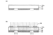
Note that the size of the
次に、図3を用いて図1に示すレーザビーム照射装置を用いた開口方法を具体的に説明する。本実施の形態では、図3に示すように、基板720上に、光吸収層として導電層721aと導電層721bとの積層膜が形成され、光透過層として絶縁層722が形成されている。
Next, an opening method using the laser beam irradiation apparatus shown in FIG. 1 will be specifically described with reference to FIG. In this embodiment mode, as illustrated in FIG. 3, a stacked film of a
導電層721a、及び導電層721bは積層構造となっており、本実施の形態は、導電層721bに比較的蒸発し易い低融点金属(本実施の形態ではクロム)を用い、導電層721aには導電層721bよりも蒸発しにくい高融点金属(本実施の形態ではタングステン)を用いる。なお、本実施の形態では絶縁層下の導電層は融点が異なる導電層を積層しているが、もちろん単層でもよい。なお、絶縁層722としてはレーザ光を透過する材料で形成された層であれば特に限定されない。例えば透光性の有機樹脂などを用いて形成することができる。
The
また、絶縁層下に設けられる層は必ずしも導電層である必要はなく、レーザアブレーションが可能な程度にレーザ光を吸収する材料で形成された層(光吸収層ともいう)であれば特に限定されない。例えば光吸収層として、チタン(Ti)、アルミニウム(Al)、タンタル(Ta)、タングステン(W)、モリブデン(Mo)、銅(Cu)、クロム(Cr)、ネオジム(Nd)、鉄(Fe)、ニッケル(Ni)、コバルト(Co)、ルテニウム(Ru)、ロジウム(Rh)、パラジウム(Pd)、オスミウム(Os)、イリジウム(Ir)、銀(Ag)、金(Au)、白金(Pt)、カドミウム(Cd)、亜鉛(Zn)、珪素(Si)、ゲルマニウム(Ge)、ジルコニウム(Zr)、バリウム(Ba)から選ばれた元素からなる材料を用いることができる。また、該元素を主成分とする合金材料、窒素化合物、酸素化合物、炭素化合物、若しくはハロゲン化合物の単層で形成することができる。また、これらの積層を用いることができる。また、光を吸収することが可能な粒子が分散された絶縁膜、代表的にはシリコン微結晶が分散された酸化ケイ素膜を用いることができる。また、色素が絶縁物に溶解または分散された絶縁層を用いることができる。光吸収層として、これらの材料で形成された層を単層又は積層して用いることができる。 The layer provided below the insulating layer is not necessarily a conductive layer, and is not particularly limited as long as it is a layer (also referred to as a light absorption layer) formed of a material that absorbs laser light to the extent that laser ablation is possible. . For example, as a light absorption layer, titanium (Ti), aluminum (Al), tantalum (Ta), tungsten (W), molybdenum (Mo), copper (Cu), chromium (Cr), neodymium (Nd), iron (Fe) , Nickel (Ni), cobalt (Co), ruthenium (Ru), rhodium (Rh), palladium (Pd), osmium (Os), iridium (Ir), silver (Ag), gold (Au), platinum (Pt) A material made of an element selected from cadmium (Cd), zinc (Zn), silicon (Si), germanium (Ge), zirconium (Zr), and barium (Ba) can be used. Alternatively, an alloy material containing the element as a main component, a nitrogen compound, an oxygen compound, a carbon compound, or a single layer of a halogen compound can be used. Further, a stack of these can be used. Alternatively, an insulating film in which particles capable of absorbing light are dispersed, typically a silicon oxide film in which silicon microcrystals are dispersed, can be used. Alternatively, an insulating layer in which a dye is dissolved or dispersed in an insulator can be used. As the light absorption layer, a layer formed of these materials can be used as a single layer or a stacked layer.
なお、光吸収層の形成方法としては、塗布法、電界メッキ法、PVD法(Physical Vapor Deposition)、又はCVD法(Chemical Vapor Deposition)を用いることができる。 In addition, as a formation method of a light absorption layer, the apply | coating method, an electroplating method, PVD method (Physical Vapor Deposition), or CVD method (Chemical Vapor Deposition) can be used.
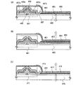
続いて、図3(B)に示すように、絶縁層722側よりレーザ光723を選択的に導電層721a、及び導電層721b(複数の照射領域724)に照射する。なお、レーザ光723は図1に示すレーザビーム照射装置から射出されている。ここで、レーザ光723は絶縁層722を透過するが導電層712bに吸収される。照射されたレーザ光のエネルギーにより導電層721bの照射領域は加熱されて蒸発し、絶縁層722を破壊する。よって、導電層721bの照射領域上の絶縁層722は除去され、導電層721a、721bの一部が露出した複数の開口725を形成することができる(図3(C)参照)。導電層721bは導電層728a、728bに分離され、絶縁層722は絶縁層727aと727bとに分離される(図3(C)参照)。続いて、導電層721a、導電層721bが露出された開口725に導電層726を形成することにより、導電層721a、導電層721bと導電層726とを電気的に接続することができる(図3(D)参照)。
Subsequently, as illustrated in FIG. 3B, the
本実施の形態のレーザビーム照射装置を用いることにより、複雑なフォトリソグラフィ工程を用いることなく複数のコンタクトホールを同時に開口することが可能となる。また、本実施の形態では、エネルギー分布が均一化された線状ビームを用いているため、ガウシアン分布のレーザビームを用いる場合に比べて、コンタクトホール開口時のレーザアブレーションに必要なプロセスマージンを広くとることが可能である。 By using the laser beam irradiation apparatus of this embodiment mode, a plurality of contact holes can be simultaneously opened without using a complicated photolithography process. In this embodiment, since a linear beam having a uniform energy distribution is used, a process margin necessary for laser ablation at the time of opening a contact hole is widened compared with a case where a laser beam having a Gaussian distribution is used. It is possible to take.
レーザ発振器1101としては、紫外光、可視光、又は赤外光を発振することが可能なレーザ発振器を用いることができる。レーザ発振器としては、KrF、ArF、XeCl、Xe等のエキシマレーザ発振器、He、He−Cd、Ar、He−Ne、HF等の気体レーザ発振器、YAG、GdVO4、YVO4、YLF、YAlO3などの結晶にCr、Nd、Er、Ho、Ce、Co、Ti又はTmをドープした結晶を使った固体レーザ発振器、GaN、GaAs、GaAlAs、InGaAsP等の半導体レーザ発振器を用いることができる。なお、固体レーザ発振器においては、基本波の第1高調波〜第5高調波を適用するのが好ましい。レーザ発振器から射出されるレーザ光の形状やレーザ光の進路を調整するため、シャッター、ミラー又はハーフミラー等の反射体、シリンドリカルレンズや凸レンズなどによって構成される光学系が設置されていてもよい。
As the
また、図1に示した装置は、基板の表面側からレーザ光を照射して露光する例を示したが、光学系や移動機構1112を適宜変更し、基板の裏面側からレーザ光を照射して露光する構成としてもよい。
The apparatus shown in FIG. 1 shows an example in which exposure is performed by irradiating a laser beam from the front side of the substrate. However, the optical system and the moving
なお、ここでは、基板を移動して選択的にレーザビームを照射しているが、これに限定されず、レーザビームをXY軸方向に走査してレーザビームを照射することができる。 Note that here, the laser beam is selectively irradiated by moving the substrate; however, the present invention is not limited to this, and the laser beam can be irradiated by scanning the laser beam in the X and Y axis directions.
導電層721a、721bは蒸着法、スパッタリング法、PVD法(Physical Vapor Deposition)、減圧CVD法(LPCVD法)、またはプラズマCVD法等のCVD法(Chemical Vapor Deposition)などを用いて形成することができる。また、構成物が所望のパターンに転写、または描写できる方法、例えば各種印刷法(スクリーン(孔版)印刷、オフセット(平版)印刷、凸版印刷やグラビア(凹版)印刷など所望なパターンで形成される方法)、ディスペンサ法、選択的な塗布法なども用いることができる。導電層721a、721bとしてクロム、モリブデン、ニッケル、チタン、コバルト、銅、又はアルミニウムのうち一種又は複数を用いて形成することができる。
The
図3においては、レーザ光723の照射によって導電層721bが蒸発し、絶縁層722に開口725を形成しており、積層される導電層721aは残存する例を示した。絶縁層下に形成された導電層に達する開口を形成する他の例を図4(A)乃至(D)に示す。なお、図4では開口部を1つ形成する例を示すが、もちろん図3に示す場合と同様に複数の開口部を同時に形成することができる。
FIG. 3 shows an example in which the
図4(A)は、絶縁層下の積層された導電層のうち上層の導電層の上方部のみがレーザ光によりレーザアブレーションされた例である。基板730上に導電層731、導電層732、絶縁層733が設けられ、導電層732、絶縁層733に形成された開口750に導電層734が設けられている。開口750において導電層732が露出され、導電層734に接して電気的に接続している。
FIG. 4A shows an example in which only the upper part of the upper conductive layer of the stacked conductive layers under the insulating layer is laser ablated by laser light. A
絶縁層下の導電層は融点が異なる複数種の導電層を積層してもよいし、もちろん単層でもよい。絶縁層下の導電層が単層の例を図4(B)(C)に示す。図4(B)は、絶縁層下の導電層の上方部のみがレーザ光によりレーザアブレーションされた例であり、図4(C)は絶縁層下の導電層において基板740が露出するまでレーザアブレーションによって除去された例である。
The conductive layer under the insulating layer may be a laminate of a plurality of types of conductive layers having different melting points, or may be a single layer. FIGS. 4B and 4C illustrate an example in which the conductive layer under the insulating layer is a single layer. FIG. 4B shows an example in which only the upper portion of the conductive layer under the insulating layer is laser ablated by laser light, and FIG. 4C shows the laser ablation until the
図4(B)において、基板735上に導電層736、絶縁層738が設けられ、導電層736、絶縁層738に形成された開口751に導電層739が設けられている。開口751において導電層736が露出され、導電層739に接して電気的に接続している。図4(B)のように導電層の膜厚方向において上方のみを部分的に除去する場合、レーザ光の照射条件(エネルギー、照射時間など)を制御するか、導電層736を厚く形成すればよい。
4B, a
図4(C)において、基板740上に導電層741a、741b、絶縁層743が設けられ、導電層744、絶縁層743に形成された開口752に導電層744が設けられている。開口752において導電層741a、741bが露出され、導電層744に接して電気的に接続している。図2(B)のように、開口底面において下部導電層と上部導電層とが必ずしも接しなくてもよく、開口の側面に露出した下部導電層に接するように上部導電層を形成し、電気的に接続する構成でもよい。
4C,
また、コンタクトホールとして機能する開口の形状も側面が底面に対して垂直でなくてもよく、図4(D)のように開口の側辺がテーパーを有する形状でもよい。図4(D)において、基板745上に導電層746、導電層747、絶縁層748が形成され、絶縁層748及び導電層747に開口753が形成されている。開口753はすり鉢状であり、開口753側面は底面に対してテーパーを有する形状となっている。
Further, the shape of the opening functioning as the contact hole may not be such that the side surface is perpendicular to the bottom surface, and the opening side may be tapered as shown in FIG. 4D, a
このように、絶縁層に設けられた開口において絶縁層下の下部導電層と絶縁層上の上部導電層とを電気的に接続させる。本実施の形態では、第1の導電層上に蒸発しやすい金属よりなる第2の導電層を形成し、レーザ光によって第2の導電層を蒸発させることによって第1の導電層及び第2の導電層上に形成された絶縁層に開口を形成する。レーザ光の照射条件(エネルギー強度、照射時間など)及び絶縁層、導電層の材料の性質(熱伝導率、融点、沸点など)によって絶縁層及び導電層に形成される開口の大きさや形状は制御することができる。レーザ光の大きさ及び形成される開口の大きさの例を図5に示す。なお、図5では開口部を1つ形成する例を示すが、もちろん図3に示す場合と同様に複数の開口部を同時に形成することができる。 Thus, the lower conductive layer below the insulating layer and the upper conductive layer on the insulating layer are electrically connected to each other through the opening provided in the insulating layer. In this embodiment mode, a second conductive layer made of a metal that easily evaporates is formed over the first conductive layer, and the second conductive layer is evaporated by laser light, whereby the first conductive layer and the second conductive layer are evaporated. An opening is formed in the insulating layer formed over the conductive layer. The size and shape of the openings formed in the insulating layer and the conductive layer are controlled by the irradiation conditions (energy intensity, irradiation time, etc.) of the laser beam and the properties of the insulating layer and the conductive layer (thermal conductivity, melting point, boiling point, etc.). can do. An example of the size of the laser beam and the size of the opening to be formed is shown in FIG. Although FIG. 5 shows an example in which one opening is formed, it is needless to say that a plurality of openings can be formed simultaneously as in the case shown in FIG.
基板300上に、第1の導電層301a(301a1、301a2、301a3)、第2の導電層301bが積層して形成され、第1の導電層301a(301a1、301a2、301a3)及び第2の導電層301bを覆うように絶縁層302が形成されている。図5において、第1の導電層301a(301a1、301a2、301a3)は複数の薄膜を含む積層構造を示し、例えば、第1の導電層301a1にチタン、第1の導電層301a2にアルミニウム、第1の導電層301a3にチタン、第2の導電層301bにクロムを用いることができる。また第1の導電層301a3にはタングステンやモリブデンなども用いることができる。勿論第2の導電層301bも積層構造とすることができ、銅とクロムの積層などを用いることができる。
A first conductive layer 301a (301a1, 301a2, 301a3) and a second
絶縁層302及び第2の導電層301bにレーザ径L1のレーザ光303を照射し、絶縁層302及び第2の導電層301bにおいて選択的に照射領域304となる。レーザ光303のエネルギーが大きいと、図5(C)のように、第2の導電層301bに与えられるエネルギーも大きくなり、第2の導電層301bにおいて照射領域及びその周辺まで熱が伝導する。よって第2の導電層301bにはレーザ光303の径L1より大きな径L2を有する開口が形成され、第2の導電層301b上に形成された絶縁層302にも開口が形成される。以上のように、第2の導電層301bは第2の導電層308a、308bに分断され、絶縁層302は絶縁層307a、307bに分断され、開口305が形成される。第1の導電層301a3が露出された開口305に導電膜306を形成し、第1の導電層301a(301a1、301a2、301a3)及び第2の導電層308a、308bと電気的に接続する(図5(D)参照)。
The insulating
レーザ光の径によって決定する照射領域に対する開口の大きさは、レーザ光のエネルギーの大きさに依存し、レーザ光のエネルギーが第2の導電層を蒸発させるのに十分な程大きいとエネルギーは照射領域周辺まで伝達し、第2の導電層を蒸発するので、第2の導電層にレーザ光の照射領域より大きな開口を形成する。逆にレーザ光のエネルギーが小さいと、第2の導電層には照射領域とほぼ同じ大きさの開口が形成される。また、第2の導電層に熱伝導率が高く蒸発しやすい金属材料を用いると、レーザ光のエネルギーが伝達しやすいので照射領域に対して大きな開口を形成することができる。なお、レーザ光のエネルギーがしきい値を超えた際には、開口の大きさはエネルギーの大きさではなくマスクの穴の径に依存する。 The size of the opening with respect to the irradiation region determined by the diameter of the laser beam depends on the energy of the laser beam, and the energy is irradiated when the energy of the laser beam is large enough to evaporate the second conductive layer. Since the second conductive layer is transmitted to the periphery of the region and the second conductive layer is evaporated, an opening larger than the region irradiated with the laser light is formed in the second conductive layer. On the other hand, when the energy of the laser beam is small, an opening having almost the same size as the irradiated region is formed in the second conductive layer. In addition, when a metal material having high thermal conductivity and easily vaporized is used for the second conductive layer, the energy of the laser beam can be easily transmitted, so that a large opening can be formed in the irradiation region. When the energy of the laser beam exceeds the threshold value, the size of the opening depends on the diameter of the mask hole, not the size of the energy.
このように、レーザ光のエネルギーを制御することによって、レーザ光が照射される第2の導電層において蒸発する範囲をある程度制御することができるため、第2の導電層及び絶縁層に形成される開口の大きさも適宜制御することができる。 In this way, by controlling the energy of the laser light, the evaporation range in the second conductive layer irradiated with the laser light can be controlled to some extent, so that it is formed in the second conductive layer and the insulating layer. The size of the opening can also be controlled as appropriate.
また、レーザ光の照射により開口を形成した後、液体で開口付近に残存する導電性材料や絶縁性材料(導電層又は絶縁層の除去された部分の残存物)を洗浄し、残存物を除去してもよい。この場合、洗浄に水などの無反応物質を用いてもよいし、絶縁層と反応する(溶解する)エッチャントなどの薬液を用いてもよい。エッチャントを用いると開口がオーバーエッチングされ、ゴミ等が除去され表面がより平坦化される。また開口を広げることもできる。 In addition, after the opening is formed by laser light irradiation, the conductive material or insulating material remaining in the vicinity of the opening with a liquid is washed to remove the residue. May be. In this case, an unreacted substance such as water may be used for cleaning, or a chemical solution such as an etchant that reacts (dissolves) with the insulating layer may be used. When an etchant is used, the opening is over-etched, dust and the like are removed, and the surface is flattened. The opening can also be widened.
本実施の形態において、線状ビームの長手方向に沿って複数の開口部が配列されたマスクの複数の開口部に同時に線状ビームを照射する。それにより、線状ビームが複数のレーザビームに分割され、該レーザビームが照射される層間絶縁層に複数のコンタクトホールを同時に形成することができる。本実施の形態のレーザ照射装置及び照射方法を用いることにより、層間絶縁層に複数のコンタクトホールを単一の工程で容易に形成することができる。 In the present embodiment, the linear beam is simultaneously irradiated to the plurality of openings of the mask in which the plurality of openings are arranged along the longitudinal direction of the linear beam. Thus, the linear beam is divided into a plurality of laser beams, and a plurality of contact holes can be formed simultaneously in the interlayer insulating layer irradiated with the laser beams. By using the laser irradiation apparatus and the irradiation method of this embodiment, a plurality of contact holes can be easily formed in the interlayer insulating layer in a single process.
本実施の形態により、コンタクトホール形成において工程数が多く煩雑なフォトリソ工程を使用する必要がないため、工程を簡略化でき、生産能力を向上させることができる。よって、材料のロスが少なく、コストダウンが達成できる。 According to the present embodiment, it is not necessary to use a complicated photolithography process with many steps in forming the contact hole, so that the process can be simplified and the production capacity can be improved. Therefore, there is little loss of material and cost reduction can be achieved.
(実施の形態2)
本実施の形態では、線状ビームを用いたレーザアブレーションによって複数のコンタクトホールを同時に開口するための実施の形態1とは異なる構成のレーザビーム照射装置について説明する。本実施の形態では、マスクとマイクロレンズアレイとを組み合わせることにより、より小さなコンタクトホールを容易に開口することができるレーザビーム照射装置について説明する。
(Embodiment 2)
In this embodiment, a laser beam irradiation apparatus having a configuration different from that in Embodiment 1 for simultaneously opening a plurality of contact holes by laser ablation using a linear beam will be described. In this embodiment mode, a laser beam irradiation apparatus that can easily open a smaller contact hole by combining a mask and a microlens array will be described.
本実施の形態のレーザビーム照射装置の一例について図6を用いて説明する。本実施の形態のレーザビーム照射装置は図6に示すように、レーザ発振器1101側から順に、光学装置1107、落射ミラー1108、ダブレットレンズ1109a、1109b、マスク1110、マイクロレンズアレイ1113を有している。なお、マイクロレンズアレイ1113は多数のレンズを配列したものであり、各レンズを通過したレーザビームを縮小して被照射体1111に投影する機能を有する。また、レーザ発振器1101、光学装置1107、落射ミラー1108、ダブレットレンズ1109a、1109b、及びマスク1110は実施の形態1と同様のものを用いることができる。なお、必ずしも落射ミラー1108又はダブレットレンズ1109a、1109bを設ける必要はなく、レーザ発振器1101から射出されたレーザビームがマスク1110面において線状ビームに整形される光学系がレーザ発振器1101とマスク1110との間に設けられていればよい。
An example of the laser beam irradiation apparatus of this embodiment will be described with reference to FIG. As shown in FIG. 6, the laser beam irradiation apparatus of this embodiment includes an
本実施の形態において、実施の形態1と同様にマスク1110面において線状ビームのエネルギー分布が均一化されるようにレーザ発振器1101、ホモジナイザが組み込まれた光学装置1107、落射ミラー1108、ダブレットレンズ1109a、1109b、及びマスク1110を配置するとよい。そして、マイクロレンズアレイ1113によってマスク1110と被照射体1111とが共役の関係になるようにマイクロレンズアレイ1113を配置する。マスク1110と被照射体1111とが共役の関係になるように配置することによって、マスク1110面におけるエネルギー分布を維持しながらに被照射体1111表面にレーザビームを照射することができる。つまり、本実施の形態においてマスク1110面でレーザビームのエネルギー分布が均一になるため、マスク1110と被照射体1111とが共役の関係になるように配置することによって、被照射面1111にエネルギー分布が均一化されたレーザビームを照射することができる。また、マスク1110を通過することにより複数に分割されたレーザビームのそれぞれが、マイクロレンズアレイ1113を構成する複数のレンズのうちの1つに入射されるようにする。
In the present embodiment, as in the first embodiment, a
このように配置することにより、マスク1110面におけるエネルギー分布を維持しながらマイクロレンズアレイ1113を介して被照射体1111表面にレーザビームを縮小投影することができる。つまり、被照射体1111表面においてエネルギー分布が均一化され、かつ縮小されたレーザビームを照射することが可能である。
With this arrangement, the laser beam can be reduced and projected onto the surface of the
なお、本実施の形態において、被照射体とは基板上に光吸収層と光透過層とを順に積層して形成したものである。本実施の形態のレーザビーム照射装置を用いて被照射体表面にレーザビームを照射することにより、複雑なフォトリソグラフィ工程を用いることなく被照射体上に複数のコンタクトホールを同時に開口することが可能となる。また、本実施の形態では、エネルギー分布が均一化された線状ビームを用いているため、ガウシアン分布のレーザビームを用いる場合に比べて、コンタクトホール開口時のレーザアブレーションに必要なプロセスマージンを広くとることが可能である。 Note that in this embodiment mode, an object to be irradiated is formed by sequentially stacking a light absorption layer and a light transmission layer over a substrate. By irradiating the surface of the irradiated object with a laser beam using the laser beam irradiation apparatus of this embodiment, a plurality of contact holes can be simultaneously opened on the irradiated object without using a complicated photolithography process. It becomes. In this embodiment, since a linear beam having a uniform energy distribution is used, a process margin necessary for laser ablation at the time of opening a contact hole is widened compared with a case where a laser beam having a Gaussian distribution is used. It is possible to take.
(実施の形態3)
本実施の形態において、レーザアブレーションによって光透過層に複数の開口部(コンタクトホール)を同時に形成するための、実施の形態1又は実施の形態2とは異なる構成のレーザビーム照射装置及びレーザームビーム照射方法を提案する。
(Embodiment 3)
In this embodiment, a laser beam irradiation apparatus and a laser beam having a configuration different from that of Embodiment 1 or
まず、レーザ光(レーザビームともいう)を処理領域に照射するレーザビーム照射装置の一例について図7を用いて説明する。図7に示すレーザビーム照射装置は、レーザ発振器1101、光学装置1107、落射ミラー1108、ダブレットレンズ1109a、1109b、マスク1110、チョッパーフィン1116とを有している。なお、必ずしも落射ミラー1108又はダブレットレンズ1109a、1109bを設ける必要はなく、レーザ発振器1101から射出されたレーザビームがマスク1110面において線状ビームに整形される光学系がレーザ発振器1101とマスク1110との間に設けられていればよい。なお、本実施の形態において、実施の形態1又は実施の形態2と同様にマスク1110面において線状ビームのエネルギー分布が均一化されるようにレーザ発振器1101、ホモジナイザが組み込まれた光学装置1107、落射ミラー1108、ダブレットレンズ1109a、1109b、及びマスク1110を配置するとよい。
First, an example of a laser beam irradiation apparatus that irradiates a processing region with laser light (also referred to as a laser beam) is described with reference to FIGS. The laser beam irradiation apparatus illustrated in FIG. 7 includes a
図7に示すレーザビーム照射装置において、レーザ発振器1101から射出されたレーザビームは、光学装置1107を通過する。次いで、落射ミラー1108にて被照射体1111に対して垂直にレーザビームが照射されるように反射される。前記落射ミラー1108にて反射されたレーザビームは、ダブレットレンズ1109aおよび1109bにて線状ビームの短辺方向が集光される。集光された線状ビームは、所望の場所にコンタクト径と同じ乃至同程度の径の穴を形成したマスク1110に至り、該マスク1110を通過したレーザビームのみがチョッパーフィン1116に至る。チョッパーフィン1116は、一部が弧状に切り取られた円形の板であり、駆動ベルト1114を介してモーター1115の回転動力が伝達されて回転する。なお、チョッパーフィン1116のような板を回転させ、連続的な光を透過・遮光を繰り返して点滅のような断続的な光に変えるものを一般的にチョッパーという。
In the laser beam irradiation apparatus shown in FIG. 7, the laser beam emitted from the
本実施の形態において、チョッパーフィン1116に伝搬されたレーザビームは、チョッパーフィン1116の弧状に切り取られた部分を通過したときのみ被照射体1111に照射され、照射されたレーザビームにより被照射体1111上に複数のコンタクトホールを同時に開口することができる。逆に、切り取られていない部分に照射されたときには、フィン部分に吸収され、被照射体1111に照射されることはない。
In this embodiment mode, the laser beam propagated to the
一般的に、線状ビームを連続的にマスク上に照射する場合において、マスクの位置を固定して被照射体のみを移動させると被照射体上にはマスクに開口された穴と同程度の大きさの穴ではなく、被照射体の移動方向に沿った線状の開口部が形成されてしまう。よって、線状ビームをマスク上に連続的に照射する場合は、マスクと被照射体とを一緒に動かす必要がある。 In general, when a linear beam is continuously irradiated onto a mask, if the position of the mask is fixed and only the irradiated object is moved, the same degree as the hole opened in the mask is formed on the irradiated object. A linear opening along the moving direction of the irradiated object is formed instead of a hole having a size. Therefore, when continuously irradiating a linear beam on a mask, it is necessary to move a mask and a to-be-irradiated body together.
しかしながら、本実施の形態のようにチョッパーフィンを用いることにより、連続的な光を断続的な光にすることができるため、マスク上に連続的に線状ビームを照射する場合においても、マスクを固定して被照射体1111のみを移動させることにより、マスクの穴の径と同じ乃至同程度の大きさのコンタクトホールを被照射体上の複数箇所に同時に形成することができる。よって、マスクサイズを小型化することができる。なお、マスク1110およびチョッパーフィン1110の材料は、レーザビームを透過しない材料であれば特に限定されない。
However, by using chopper fins as in this embodiment, continuous light can be made intermittent light. Therefore, even when a linear beam is continuously irradiated on the mask, the mask is By fixing and moving only the object to be irradiated 1111, contact holes having the same or the same size as the hole diameter of the mask can be simultaneously formed at a plurality of locations on the object to be irradiated. Therefore, the mask size can be reduced. Note that the material of the
続いて、移動機構1112及びマスク1110が図7中の矢印の方向に一定速度で移動することにより、被照射体1111全体をレーザ照射することができる。本実施の形態において移動機構1112はXYステージであり、X軸又はY軸方向に移動する機構を有する。なお、回転する機構を有していてもよい。なお、本実施の形態において、被照射体とは基板上に光吸収層と光透過層とを順に積層して形成したものである。
Subsequently, the
本実施の形態では、線状ビームをマスク1110に形成された複数箇所の穴に同時に照射できるため、該線状ビームをマスクを介して複数のレーザビームに分割することができる。よって、被照射体1111上の複数箇所に一度にレーザビームを照射することができる。従って、本実施の形態のレーザビーム照射装置を用いて被照射体1111表面にレーザビームを照射することにより、複雑なフォトリソグラフィ工程を用いることなく被照射体1111上に複数のコンタクトホールを同時に開口することが可能となる。また、チョッパーを採用したことにより、レーザビームを照射する時間をコントロールできるため、例えば1列に並んだコンタクトホールを基板全面に連続して開口する場合には、該1列分の穴が開いたマスクを用意すれば良く、マスクサイズの小型化につながる。
In this embodiment mode, a linear beam can be simultaneously irradiated to a plurality of holes formed in the
(実施の形態4)
線状ビームを用いたレーザアブレーションによって複数のコンタクトホールを同時に開口する際に、該線状ビームを複数に分割するために用いることが可能なマスクとして実施の形態1〜3で示したもの以外にも様々な構成のものを用いることができる。本実施の形態では、該線状ビームを複数に分割するために用いることが可能なマスクの例について図面を用いて説明する。なお、本実施の形態で示したマスクは、実施の形態1〜3で示したマスクのかわりに適宜用いることが可能である。
(Embodiment 4)
Other than the masks shown in the first to third embodiments as masks that can be used to divide the linear beam into a plurality of holes when simultaneously opening a plurality of contact holes by laser ablation using a linear beam. Also, various configurations can be used. In this embodiment, an example of a mask that can be used to divide the linear beam into a plurality of parts will be described with reference to the drawings. Note that the mask described in this embodiment can be used as appropriate instead of the mask described in any of Embodiments 1 to 3.
本実施の形態のマスクとして、図8(A)に示すようなバイナリーマスク121aを用いることができる。バイナリーマスク121aは、石英等の透光性を有する基板122上に、クロムや酸化クロム等の光を吸収する遮光層123が選択的に形成されている。遮光層123が形成されない領域において光を透過することができる。
As a mask in this embodiment, a
また、光吸収層に照射されるレーザビームのエネルギーが高いとき、図8(B)に示すように、透光性を有する基板122及び遮光層123の間に反射層124を形成することが好ましい。反射層124を設けることにより、遮光層におけるレーザビームの吸収量を低減することができる。このため、レーザビーム104の光吸収によるエネルギーの熱転化及び当該熱よる遮光層のパターンが変形することを回避することができる。
In addition, when the energy of the laser beam applied to the light absorption layer is high, a
なお、反射層124としては、誘電体ミラーや反射性を有する層を用いることができる。誘電体ミラーとは、屈折率の異なる2種類の透明な絶縁層を交互に積層したものである。このとき2種類の透明な絶縁層の屈折率が大きいほど、また層数が多いほど反射効率は高くなる。なお、誘電体ミラーは照射されるレーザビームの波長により適宜積層する材料を選択する。例えば可視光を反射する誘電体ミラーの積層構造としては、二酸化チタン及び二酸化珪素の積層構造、硫化亜鉛及びフッ化マグネシウムの積層構造、アモルファスシリコン及び窒化珪素の積層構造などがある。
As the
また、反射性を有する層として、アルミニウム、金、銀、ニッケル等で形成される層を用いてもよい。さらには、誘電体ミラー及び反射性を有する層を積層させてもよい。 Alternatively, a layer formed of aluminum, gold, silver, nickel, or the like may be used as the reflective layer. Furthermore, a dielectric mirror and a reflective layer may be stacked.
バイナリーマスクを用いることにより、該線状ビームを複数のレーザビームに分割することができる。よって、被照射体上の複数箇所に一度にレーザビームを照射することができる。 By using a binary mask, the linear beam can be divided into a plurality of laser beams. Therefore, a laser beam can be irradiated to a plurality of locations on the irradiated object at a time.
また、本実施の形態のマスクとして、位相シフトマスクを用いることができる。位相シフトマスクを用いることにより、微細な形状、代表的には幅が小さい層、または幅及び長さが小さい層を形成することができる。 Further, a phase shift mask can be used as the mask in this embodiment. By using a phase shift mask, a fine shape, typically a layer with a small width, or a layer with a small width and length can be formed.
位相シフトマスクとして例えば、レベンソン型シフトマスクを用いることができる。レベンソン型シフトマスクとは、図9(A)に示す位相シフトマスク131のように多数の細かい凹凸が周期的に基板表面に形成されたものである。当該凹凸により、位相シフトマスクを透過するレーザビームの位相を変調し、部分的に消滅干渉を生じさせて、レーザビームの強度の周期を変調することが可能である。ここでは、隣接する凹凸の間で位相差が180°となるような凹凸を設ける。この結果、図9(B)に示すように、位相132に180°の差がでる。これらの光が干渉することにより、位相シフトマスク131を通過したレーザビームは図9(C)に示すようなレーザビームの強度分布133を有する。
For example, a Levenson-type shift mask can be used as the phase shift mask. The Levenson-type shift mask is one in which a large number of fine irregularities are periodically formed on the substrate surface as in the
図9(C)に示すようなレーザビームを、図9(A)に示すように絶縁層722、光吸収層721に照射することで、光吸収層にレーザビームが吸収される領域と吸収されない領域の差を十分に確保することができる。この結果、図9(D)に示すように、基板20上に形成された光吸収層721、絶縁層722に同時に複数の開口を形成することが可能である。
When the insulating
なお、図9においては、透光性を有する基板の表面に凹凸を形成してレーザビームの位相差を形成する形態を示したが、これの代わりに、遮光層及び位相シフタ材を用いてレーザビームの位相差を形成する位相シフトマスクを用いることができる。また、バイナリーマスクと位相シフトマスクを組み合わせて用いることも可能である。 Note that although FIG. 9 shows a mode in which irregularities are formed on the surface of a light-transmitting substrate to form a phase difference of a laser beam, a laser using a light shielding layer and a phase shifter material is used instead. A phase shift mask that forms the phase difference of the beam can be used. It is also possible to use a combination of a binary mask and a phase shift mask.
次に、位相シフトマスクとしてハーフトーン型シフトマスクについて説明する。 Next, a halftone shift mask will be described as a phase shift mask.
ハーフトーン型位相シフトマスク160は、図10(A)に示すように、石英等の透光性を有する基板122上に、遮光層の代わりに半透過性の位相シフタ材162が選択的に形成されている。このときのレーザビームの振幅分布163は、図10(B)に示すように、位相シフタ材162を通過した光の位相は、位相シフタ材162がない領域を通過した光に対して反転する。この結果、図10(C)で示すように、位相シフタ材162の界面では、レーザビームの強度分布164が急峻に増加する。
As shown in FIG. 10A, the halftone
図10(C)に示すような強度分布を有するレーザビームを光吸収層103に照射することで、光吸収層にレーザビームが吸収される領域と吸収されない領域の差を十分に確保することができる。この結果、図10(D)に示すように、基板720上に形成された光吸収層721、絶縁層722に微細な幅の開口を形成することができる。
By irradiating the light absorption layer 103 with a laser beam having an intensity distribution as shown in FIG. 10C, a sufficient difference between a region where the laser beam is absorbed and a region where the laser beam is not absorbed can be secured sufficiently. it can. As a result, as illustrated in FIG. 10D, an opening with a minute width can be formed in the
また、本実施の形態のマスクとして、マイクロレンズまたはマイクロレンズアレイ等の少なくとも頂部周辺に曲率を有し、好ましく全体が凸レンズのように半球状であるマイクロレンズを有するマスクを用いることができる。図11においては、マイクロレンズアレイを有するマスクについて説明する。 Further, as the mask of this embodiment, a mask having a microlens having a curvature around at least the apex, such as a microlens or a microlens array, and preferably a semi-spherical microlens like a convex lens can be used. In FIG. 11, a mask having a microlens array will be described.
マスク171の表面には、マイクロレンズアレイが形成される。また、レーザビームを照射する必要のない領域においては、遮光層173を設けている。なお、遮光層173は、図8(B)に示す反射層124と同様の材料で形成することができる。
A microlens array is formed on the surface of the
図11(A)に示すように、マスク171及び透光性を有する絶縁層722を介して光吸収層721にレーザビーム104を照射する。レーザビーム104の一部は遮光層173で遮光される。また、マイクロレンズアレイの各レンズおいて光が集光される。このため、集光されたレーザビーム104が選択的に光吸収層721に照射される。
As shown in FIG. 11A, the
この結果、図11(B)に示すように、基板720上に形成された光吸収層721、絶縁層722に微細な開口を形成することができる。
As a result, as illustrated in FIG. 11B, minute openings can be formed in the
なお、マイクロレンズアレイの代わりに、透明な基板上に選択的に透明な組成物を吐出し焼成してマイクロレンズを形成してもよい。このようなマイクロレンズは、ポリイミド、アクリル、酢酸ビニル樹脂、ポリビニルアセタール、ポリスチレン、AS樹脂、メタクリル樹脂、ポリプロピレン、ポリカーボネート、セルロイド、酢酸繊維素プラスチック、ポリエチレン、メチルペンテン樹脂、塩化ビニル樹脂、ポリエステル樹脂、ユリア樹脂で形成することができる。また、PSG(リンガラス)、BPSG(リンボロンガラス)、シリケート系SOG(Spin on Glass)、ポリシラザン系SOGや、アルコキシシリケート系SOG、ポリメチルシロキサン等に代表されるSi−CH3結合を有するSiO2で形成することができる。 Instead of the microlens array, a microlens may be formed by selectively discharging and baking a transparent composition on a transparent substrate. Such microlenses are polyimide, acrylic, vinyl acetate resin, polyvinyl acetal, polystyrene, AS resin, methacrylic resin, polypropylene, polycarbonate, celluloid, cellulose acetate plastic, polyethylene, methylpentene resin, vinyl chloride resin, polyester resin, It can be formed of urea resin. Further, SiO having Si—CH 3 bond represented by PSG (phosphorus glass), BPSG (phosphorus boron glass), silicate-based SOG (Spin on Glass), polysilazane-based SOG, alkoxysilicate-based SOG, polymethylsiloxane and the like. 2 can be formed.
本実施の形態で示すようなマスクを用いて線状ビームを分割することにより、基板上に形成された光吸収層に同時に複数の微細な開口を選択的に形成することができる。この結果、半導体装置の微細化が可能となる。 By dividing a linear beam using a mask as shown in this embodiment mode, a plurality of fine openings can be selectively formed in the light absorption layer formed over the substrate at the same time. As a result, the semiconductor device can be miniaturized.
(実施の形態5)
本実施の形態では、実施の形態1〜4に示したレーザビーム照射装置及び照射方法を用いて表示装置を作製する方法を説明する。
(Embodiment 5)
In this embodiment, a method for manufacturing a display device using the laser beam irradiation apparatus and the irradiation method described in any of Embodiments 1 to 4 will be described.
図12(A)は本実施の形態の表示パネルの構成を示す上面図であり、絶縁表面を有する基板2700上に画素2702をマトリクス上に配列させた画素部2701、走査線側入力端子2703、信号線側入力端子2704が形成されている。画素数は種々の規格に従って設ければ良く、XGAであってRGBを用いたフルカラー表示であれば1024×768×3(RGB)、UXGAであってRGBを用いたフルカラー表示であれば1600×1200×3(RGB)、フルスペックハイビジョンに対応させ、RGBを用いたフルカラー表示であれば1920×1080×3(RGB)とすれば良い。
12A is a top view illustrating the structure of the display panel of this embodiment. A
画素2702は、走査線側入力端子2703から延在する走査線と、信号線側入力端子2704から延在する信号線とが交差することで、マトリクス状に配設される。画素2702のそれぞれには、スイッチング素子とそれに接続する画素電極が備えられている。スイッチング素子の代表的な一例はTFTであり、TFTのゲート電極側が走査線と、ソース若しくはドレイン側が信号線と接続されることにより、個々の画素を外部から入力する信号によって独立して制御可能としている。
The
図12(A)は、走査線及び信号線へ入力する信号を、外付けの駆動回路により制御する表示パネルの構成を示しているが、図12(A)に示すように、COG(Chip on Glass)方式によりドライバIC2751を基板2700上に実装しても良い。また他の実装形態として、図12(B)に示すようなTAB(Tape Automated Bonding)方式を用いてもよい。ドライバICは単結晶半導体基板に形成されたものでも良いし、ガラス基板上にTFTで回路を形成したものであっても良い。図12において、ドライバIC2751は、FPC2750と接続している。また、画素に設けるTFTを、結晶性が高い多結晶(微結晶)半導体で形成する場合には、走査線側の駆動回路を基板上に形成することもできる。画素に設けるTFTを移動度の高い、多結晶(微結晶)半導体、単結晶半導体などで形成する場合は、走査線の駆動回路と信号線駆動回路とを基板上に一体形成することもできる。
FIG. 12A shows a structure of a display panel in which signals input to the scan lines and signal lines are controlled by an external driver circuit. As shown in FIG. 12A, COG (Chip on The
次に、図13乃至図20を用いて逆スタガ型の薄膜トランジスタを有する表示装置の作製方法について説明する。なお、図13乃至図19の(A)は表示装置画素部の上面図であり、図13乃至図19の(B)は、図13乃至図19の(A)のAとCとを結ぶ破線における断面図、(C)はBとDとを結ぶ破線における断面図である。また、図20(A)(B)は表示装置の断面図である。 Next, a method for manufacturing a display device having an inverted staggered thin film transistor will be described with reference to FIGS. 13A to 19A are top views of the display device pixel portion, and FIGS. 13B to 19B are broken lines connecting A and C in FIGS. 13A to 19A. (C) is sectional drawing in the broken line which ties B and D in FIG. 20A and 20B are cross-sectional views of the display device.
基板100は、バリウムホウケイ酸ガラス、アルミノホウケイ酸ガラス等からなるガラス基板、石英基板、金属基板、又は本作製工程の処理温度に耐えうる耐熱性を有するプラスチック基板を用いる。また、基板100の表面が平坦化されるようにCMP法などによって、研磨しても良い。なお、基板100上に、絶縁層を形成してもよい。絶縁層は、CVD法、プラズマCVD法、スパッタリング法、スピンコート法等の種々の方法により、珪素を含む酸化物材料、窒化物材料を用いて、単層又は積層して形成される。この絶縁層は、形成しなくても良いが、基板100からの汚染物質などを遮断する効果がある。
As the
基板100上に、導電膜101を形成する。導電膜101は、スパッタリング法、PVD法(Physical Vapor Deposition)、減圧CVD法(LPCVD法)、またはプラズマCVD法等のCVD法(Chemical Vapor Deposition)などを用いて形成することができる。導電膜101は、Ag、Au、Ni、Pt、Pd、Ir、Rh、Ta、W、Ti、Mo、Al、Cuから選ばれた元素、又は前記元素を主成分とする合金材料もしくは化合物材料で形成すればよい。また、リン等の不純物元素をドーピングした多結晶シリコン膜に代表される半導体膜や、AgPdCu合金を用いてもよい。また、単層構造でも複数層の構造でもよく、例えば、窒化タングステン(WN)膜とモリブデン(Mo)膜との2層構造としてもよいし、膜厚50nmのタングステン膜、膜厚500nmのアルミニウムとシリコンの合金(Al−Si)膜、膜厚30nmの窒化チタン膜を順次積層した3層構造としてもよい。また、3層構造とする場合、第1の導電膜のタングステンに代えて窒化タングステンを用いてもよいし、第2の導電膜のアルミニウムとシリコンの合金(Al−Si)膜に代えてアルミニウムとチタンの合金膜(Al−Ti)を用いてもよいし、第3の導電膜の窒化チタン膜に代えてチタン膜を用いてもよい。
A conductive film 101 is formed over the
本実施の形態ではゲート電極層は組成物を選択的に吐出して形成する。このように選択的にゲート電極層を形成すると加工の工程が簡略化する効果がある。 In this embodiment mode, the gate electrode layer is formed by selectively discharging a composition. When the gate electrode layer is selectively formed in this way, there is an effect that the processing step is simplified.
本実施の形態では、導電層の形成領域の大きさ及び形状に応じて、液滴吐出装置の吐出口から組成物の吐出方法が異なることを特徴とする。比較的広範囲にわたって形成されるゲート配線に相当するゲート電極層104(104a、104b)は、図13に示すように、液滴吐出装置136a、136bからの組成物の吐出が停止することなく、連続的に吐出させて形成する。一方、比較的狭い範囲に形成されるゲート電極層105(105a、105b)は、図13に示すように、液滴吐出装置137a、137bからの組成物を滴下して形成する。このように形成するパターンによって、液状の組成物の吐出方法を異ならせてもよい。
The present embodiment is characterized in that the method for discharging the composition from the discharge port of the droplet discharge device differs depending on the size and shape of the conductive layer formation region. As shown in FIG. 13, the gate electrode layer 104 (104a, 104b) corresponding to the gate wiring formed over a relatively wide range is continuously discharged without stopping the discharge of the composition from the
ゲート電極層104(104a、104b)及びゲート電極層105(105a、105b)は、Ag、Au、Ni、Pt、Pd、Ir、Rh、Ta、W、Ti、Mo、Al、Cuから選ばれた元素、又は前記元素を主成分とする合金材料もしくは化合物材料で形成すればよい。また、前記元素の混合物を用いてもよい。単層構造のみならず、2層以上の積層構造としてもよい。 The gate electrode layer 104 (104a, 104b) and the gate electrode layer 105 (105a, 105b) were selected from Ag, Au, Ni, Pt, Pd, Ir, Rh, Ta, W, Ti, Mo, Al, Cu. What is necessary is just to form with the alloy material or compound material which has an element or the said element as a main component. Further, a mixture of the above elements may be used. Not only a single layer structure but also a laminated structure of two or more layers may be used.
なお、ゲート電極層104(104a、104b)及びゲート電極層105(105a、105b)の形状に加工が必要な場合、マスク層を形成し、ドライエッチングまたはドライエッチングによりエッチング加工すればよい。ICP(Inductively Coupled Plasma:誘導結合型プラズマ)エッチング法を用い、エッチング条件(コイル型の電極に印加される電力量、基板側の電極に印加される電力量、基板側の電極温度等)を適宜調節することにより、電極層をテーパー形状にエッチングすることができる。なお、エッチング用ガスとしては、Cl2、BCl3、SiCl4もしくはCCl4などを代表とする塩素系ガス、CF4、SF6もしくはNF3などを代表とするフッ素系ガス又はO2を適宜用いることができる。 Note that when the gate electrode layer 104 (104a, 104b) and the gate electrode layer 105 (105a, 105b) need to be processed, a mask layer may be formed and etched by dry etching or dry etching. Using an ICP (Inductively Coupled Plasma) etching method, the etching conditions (the amount of power applied to the coil-type electrode, the amount of power applied to the substrate-side electrode, the electrode temperature on the substrate side, etc.) are appropriately set. By adjusting, the electrode layer can be etched into a tapered shape. As an etching gas, a chlorine-based gas typified by Cl 2 , BCl 3 , SiCl 4, CCl 4, etc., a fluorine-based gas typified by CF 4 , SF 6, NF 3, etc., or O 2 is appropriately used. be able to.
マスク層は、エポキシ樹脂、フェノール樹脂、ノボラック樹脂、アクリル樹脂、メラミン樹脂、ウレタン樹脂等の樹脂材料を用いることができる。また、ベンゾシクロブテン、パリレン、フッ化アリレンエーテル、透過性を有するポリイミドなどの有機材料、シロキサン系ポリマー等の重合によってできた化合物材料、水溶性ホモポリマーと水溶性共重合体を含む組成物材料等を用いて液滴吐出法で形成する。或いは、感光剤を含む市販のレジスト材料を用いてもよく、例えば、代表的なポジ型レジストである、ノボラック樹脂と感光剤であるナフトキノンジアジド化合物、ネガ型レジストであるベース樹脂、ジフェニルシランジオール及び酸発生剤などを用いてもよい。いずれの材料を用いるとしても、その表面張力と粘度は、溶媒の濃度を調整したり、界面活性剤等を加えたりして適宜調整する。 For the mask layer, a resin material such as an epoxy resin, a phenol resin, a novolac resin, an acrylic resin, a melamine resin, or a urethane resin can be used. In addition, a composition comprising an organic material such as benzocyclobutene, parylene, fluorinated arylene ether, permeable polyimide, a compound material obtained by polymerization of a siloxane polymer, a water-soluble homopolymer and a water-soluble copolymer It is formed by a droplet discharge method using a material or the like. Alternatively, a commercially available resist material containing a photosensitizer may be used. For example, a novolak resin that is a typical positive resist and a naphthoquinonediazide compound that is a photosensitizer, a base resin that is a negative resist, diphenylsilanediol, and An acid generator or the like may be used. Whichever material is used, the surface tension and viscosity are appropriately adjusted by adjusting the concentration of the solvent or adding a surfactant or the like.
次に、ゲート電極層104a、104b、105a、105bの上にゲート絶縁層106を形成する(図14)。ゲート絶縁層106としては、珪素の酸化物材料又は窒化物材料等の材料で形成すればよく、積層でも単層でもよい。本実施の形態では、窒化珪素膜、酸化珪素膜の2層の積層を用いる。またそれらや、酸化窒化珪素膜の単層、3層以上からなる積層でも良い。好適には、緻密な膜質を有する窒化珪素膜を用いるとよい。また、液滴吐出法で形成される導電層に銀や銅などを用いる場合、その上にバリア膜として窒化珪素膜やNiB膜を形成すると、不純物の拡散を防ぎ、表面を平坦化する効果がある。なお、低い成膜温度でゲートリーク電流の少ない緻密な絶縁膜を形成するには、アルゴンなどの希ガス元素を反応ガスに含ませ、形成される絶縁膜中に混入させると良い。
Next, the
次に半導体層を形成する。一導電性型を有する半導体層は必要に応じて形成すればよい。またn型を有する半導体層を形成し、nチャネル型TFTのNMOS構造、p型を有する半導体層を形成したpチャネル型TFTのPMOS構造、nチャネル型TFTとpチャネル型TFTとのCMOS構造を作製することができる。また、導電性を付与するために、導電性を付与する元素をドーピングによって添加し、不純物領域を半導体層に形成することで、nチャネル型TFT、pチャネル型TFTを形成することもできる。n型を有する半導体層を形成するかわりに、PH3ガスによるプラズマ処理を行うことによって、半導体層に導電性を付与してもよい。 Next, a semiconductor layer is formed. A semiconductor layer having one conductivity type may be formed as necessary. In addition, an n-type semiconductor layer is formed, an n-channel TFT NMOS structure, a p-channel TFT PMOS structure having a p-type semiconductor layer, and an n-channel TFT and p-channel TFT CMOS structure. Can be produced. Further, in order to impart conductivity, an n-channel TFT or a p-channel TFT can be formed by adding an element imparting conductivity by doping and forming an impurity region in the semiconductor layer. Instead of forming an n-type semiconductor layer, conductivity may be imparted to the semiconductor layer by performing plasma treatment with a PH 3 gas.
半導体層を形成する材料は、シランやゲルマンに代表される半導体材料ガスを用いて気相成長法やスパッタリング法で作製されるアモルファス半導体(以下「AS」ともいう。)、該非晶質半導体を光エネルギーや熱エネルギーを利用して結晶化させた多結晶半導体、或いはセミアモルファス(微結晶若しくはマイクロクリスタルとも呼ばれる。以下「SAS」ともいう。)半導体などを用いることができる。半導体層は各種手段(スパッタ法、LPCVD法、またはプラズマCVD法等)により成膜することができる。 As a material for forming the semiconductor layer, an amorphous semiconductor (hereinafter also referred to as “AS”) manufactured by a vapor deposition method or a sputtering method using a semiconductor material gas typified by silane or germane is used. A polycrystalline semiconductor crystallized using energy or thermal energy, a semi-amorphous (also referred to as microcrystal or microcrystal, hereinafter, also referred to as “SAS”) semiconductor, or the like can be used. The semiconductor layer can be formed by various means (such as sputtering, LPCVD, or plasma CVD).
SASは、非晶質と結晶構造(単結晶、多結晶を含む)の中間的な構造を有し、自由エネルギー的に安定な第3の状態を有する半導体であって、短距離秩序を持ち格子歪みを有する結晶質な領域を含んでいる。少なくとも膜中の一部の領域には、0.5〜20nmの結晶領域を観測することが出来、珪素を主成分とする場合にはラマンスペクトルが520cm−1よりも低波数側にシフトしている。X線回折では珪素結晶格子に由来するとされる(111)、(220)の回折ピークが観測される。未結合手(ダングリングボンド)を終端化するため水素またはハロゲンを少なくとも1原子%またはそれ以上含ませている。SASは、珪素を含む気体をグロー放電分解(プラズマCVD)して形成する。珪素を含む気体としては、SiH4、その他にもSi2H6、SiH2Cl2、SiHCl3、SiCl4、SiF4などを用いることが可能である。またF2、GeF4を混合させても良い。この珪素を含む気体をH2、又は、H2とHe、Ar、Kr、Neから選ばれた一種または複数種の希ガス元素で希釈しても良い。希釈率は2〜1000倍の範囲、圧力は概略0.1Pa〜133Paの範囲、電源周波数は1MHz〜120MHz、好ましくは13MHz〜60MHzである。基板加熱温度は300℃以下が好ましく、100〜200℃の基板加熱温度でも形成可能である。ここで、主に成膜時に取り込まれる不純物元素として、酸素、窒素、炭素などの大気成分に由来する不純物は1×1020cm−3以下とすることが望ましく、特に、酸素濃度は5×1019cm−3以下、好ましくは1×1019cm−3以下となるようにすることが好ましい。また、ヘリウム、アルゴン、クリプトン、ネオンなどの希ガス元素を含ませて格子歪みをさらに助長させることで安定性が増し良好なSASが得られる。また半導体層としてフッ素系ガスより形成されるSAS層に水素系ガスより形成されるSAS層を積層してもよい。 SAS is a semiconductor having an intermediate structure between amorphous and crystalline structures (including single crystal and polycrystal) and having a third state that is stable in terms of free energy and has a short-range order and a lattice. It includes a crystalline region with strain. A crystal region of 0.5 to 20 nm can be observed in at least a part of the film, and when silicon is a main component, the Raman spectrum is shifted to a lower wave number side than 520 cm −1. Yes. In X-ray diffraction, diffraction peaks of (111) and (220) that are derived from the silicon crystal lattice are observed. In order to terminate dangling bonds (dangling bonds), hydrogen or halogen is contained at least 1 atomic% or more. SAS is formed by glow discharge decomposition (plasma CVD) of a gas containing silicon. As a gas containing silicon, SiH 4 , Si 2 H 6 , SiH 2 Cl 2 , SiHCl 3 , SiCl 4 , SiF 4, or the like can be used. Further, F 2 and GeF 4 may be mixed. The gas containing silicon may be diluted with H 2 , or H 2 and one or more kinds of rare gas elements selected from He, Ar, Kr, and Ne. The dilution rate is in the range of 2 to 1000 times, the pressure is in the range of approximately 0.1 Pa to 133 Pa, and the power supply frequency is 1 MHz to 120 MHz, preferably 13 MHz to 60 MHz. The substrate heating temperature is preferably 300 ° C. or lower, and can be formed even at a substrate heating temperature of 100 to 200 ° C. Here, as an impurity element mainly taken in at the time of film formation, impurities derived from atmospheric components such as oxygen, nitrogen, and carbon are preferably 1 × 10 20 cm −3 or less, and in particular, the oxygen concentration is 5 × 10 5. It is preferable to be 19 cm −3 or less, preferably 1 × 10 19 cm −3 or less. Further, by adding a rare gas element such as helium, argon, krypton, or neon to further promote lattice distortion, stability is improved and a favorable SAS can be obtained. In addition, a SAS layer formed of a hydrogen-based gas may be stacked on a SAS layer formed of a fluorine-based gas as a semiconductor layer.
アモルファス半導体としては、代表的には水素化アモルファスシリコン、結晶性半導体としては代表的にはポリシリコンなどがあげられる。ポリシリコン(多結晶シリコン)には、800℃以上のプロセス温度を経て形成されるポリシリコンを主材料として用いた所謂高温ポリシリコンや、600℃以下のプロセス温度で形成されるポリシリコンを主材料として用いた所謂低温ポリシリコン、また結晶化を促進する元素などを添加し結晶化させたポリシリコンなどを含んでいる。もちろん、前述したように、セミアモルファス半導体又は半導体層の一部に結晶相を含む半導体を用いることもできる。 A typical example of an amorphous semiconductor is hydrogenated amorphous silicon, and a typical example of a crystalline semiconductor is polysilicon. Polysilicon (polycrystalline silicon) is mainly made of so-called high-temperature polysilicon using polysilicon formed through a process temperature of 800 ° C. or higher as a main material, or polysilicon formed at a process temperature of 600 ° C. or lower. And so-called low-temperature polysilicon, and polysilicon crystallized by adding an element that promotes crystallization. Of course, as described above, a semi-amorphous semiconductor or a semiconductor including a crystal phase in a part of the semiconductor layer can also be used.
半導体層に、結晶性半導体層を用いる場合、その結晶性半導体層の作製方法は、各種方法(レーザ結晶化法、熱結晶化法、またはニッケルなどの結晶化を助長する元素を用いた熱結晶化法等)を用いれば良い。また、SASである微結晶半導体をレーザ照射して結晶化し、結晶性を高めることもできる。結晶化を助長する元素を導入しない場合は、非晶質珪素膜にレーザ光を照射する前に、窒素雰囲気下500℃で1時間加熱することによって非晶質珪素膜の含有水素濃度を1×10²⁰atoms/cm3以下にまで放出させる。これは水素を多く含んだ非晶質珪素膜にレーザ光を照射すると非晶質珪素膜が破壊されてしまうからである。 When a crystalline semiconductor layer is used for the semiconductor layer, the crystalline semiconductor layer can be manufactured by various methods (laser crystallization, thermal crystallization, or thermal crystallization using an element that promotes crystallization such as nickel. Or the like) may be used. In addition, a microcrystalline semiconductor that is a SAS can be crystallized by laser irradiation to improve crystallinity. In the case where an element for promoting crystallization is not introduced, the amorphous silicon film is heated at 500 ° C. for 1 hour in a nitrogen atmosphere before irradiating the amorphous silicon film with laser light, whereby the concentration of hydrogen contained in the amorphous silicon film is set to 1 ×. Release to 10 20 atoms / cm 3 or less. This is because the amorphous silicon film is destroyed when the amorphous silicon film containing a large amount of hydrogen is irradiated with laser light.
非晶質半導体層への金属元素の導入の仕方としては、当該金属元素を非晶質半導体層の表面又はその内部に存在させ得る手法であれば特に限定はなく、例えばスパッタ法、CVD法、プラズマ処理法(プラズマCVD法も含む)、吸着法、金属塩の溶液を塗布する方法を使用することができる。このうち溶液を用いる方法は簡便であり、金属元素の濃度調整が容易であるという点で有用である。また、このとき非晶質半導体層の表面の濡れ性を改善し、非晶質半導体層の表面全体に水溶液を行き渡らせるため、酸素雰囲気中でのUV光の照射、熱酸化法、ヒドロキシラジカルを含むオゾン水又は過酸化水素による処理等により、酸化膜を成膜することが望ましい。 The method of introducing the metal element into the amorphous semiconductor layer is not particularly limited as long as the metal element can be present on the surface of the amorphous semiconductor layer or inside the amorphous semiconductor layer. For example, sputtering, CVD, A plasma treatment method (including a plasma CVD method), an adsorption method, or a method of applying a metal salt solution can be used. Among these, the method using a solution is simple and useful in that the concentration of the metal element can be easily adjusted. At this time, in order to improve the wettability of the surface of the amorphous semiconductor layer and to spread the aqueous solution over the entire surface of the amorphous semiconductor layer, irradiation with UV light in an oxygen atmosphere, thermal oxidation method, hydroxy radical It is desirable to form an oxide film by treatment with ozone water or hydrogen peroxide.
非晶質半導体層の結晶化は、熱処理とレーザ光照射による結晶化を組み合わせてもよく、熱処理やレーザ光照射を単独で、複数回行っても良い。 The crystallization of the amorphous semiconductor layer may be a combination of heat treatment and crystallization by laser light irradiation, or may be performed multiple times by heat treatment or laser light irradiation alone.
また、結晶性半導体層を、直接基板にプラズマ法により形成しても良い。また、線状プラズマ法を用いて、結晶性半導体層を選択的に基板に形成してもよい。 Alternatively, the crystalline semiconductor layer may be directly formed over the substrate by a plasma method. Alternatively, the crystalline semiconductor layer may be selectively formed over the substrate by a linear plasma method.
半導体として、有機半導体材料を用い、印刷法、ディスペンサ法、スプレー法、スピン塗布法、液滴吐出法などで形成することができる。この場合、上記エッチング工程が必要ないため、工程数を削減することが可能である。有機半導体としては、低分子材料、高分子材料などが用いられ、有機色素、導電性高分子材料などの材料も用いることができる。本発明に用いる有機半導体材料としては、その骨格が共役二重結合から構成されるπ電子共役系の高分子材料が望ましい。代表的には、ポリチオフェン、ポリフルオレン、ポリ(3−アルキルチオフェン)、ポリチオフェン誘導体、ペンタセン等の可溶性の高分子材料を用いることができる。 As a semiconductor, an organic semiconductor material can be used and formed by a printing method, a dispenser method, a spray method, a spin coating method, a droplet discharge method, or the like. In this case, the number of processes can be reduced because the etching process is not necessary. As the organic semiconductor, a low molecular material, a polymer material, or the like is used, and materials such as an organic dye or a conductive polymer material can also be used. The organic semiconductor material used in the present invention is preferably a π-electron conjugated polymer material whose skeleton is composed of conjugated double bonds. Typically, a soluble polymer material such as polythiophene, polyfluorene, poly (3-alkylthiophene), a polythiophene derivative, or pentacene can be used.
その他にも本発明に用いることができる有機半導体材料としては、可溶性の前駆体を成膜した後で処理することにより半導体層を形成することができる材料がある。なお、このような有機半導体材料としては、ポリチエニレンビニレン、ポリ(2,5−チエニレンビニレン)、ポリアセチレン、ポリアセチレン誘導体、ポリアリレンビニレンなどがある。 In addition, as an organic semiconductor material that can be used in the present invention, there is a material that can form a semiconductor layer by processing after forming a soluble precursor. Examples of such an organic semiconductor material include polythienylene vinylene, poly (2,5-thienylene vinylene), polyacetylene, a polyacetylene derivative, and polyarylene vinylene.
前駆体を有機半導体に変換する際には、加熱処理だけではなく塩化水素ガスなどの反応触媒を添加することがなされる。また、これらの可溶性有機半導体材料を溶解させる代表的な溶媒としては、トルエン、キシレン、クロロベンゼン、ジクロロベンゼン、アニソール、クロロフォルム、ジクロロメタン、γブチルラクトン、ブチルセルソルブ、シクロヘキサン、NMP(N−メチル−2−ピロリドン)、シクロヘキサノン、2−ブタノン、ジオキサン、ジメチルホルムアミド(DMF)または、THF(テトラヒドロフラン)などを適用することができる。 When converting the precursor into an organic semiconductor, a reaction catalyst such as hydrogen chloride gas is added as well as heat treatment. Typical solvents for dissolving these soluble organic semiconductor materials include toluene, xylene, chlorobenzene, dichlorobenzene, anisole, chloroform, dichloromethane, γ-butyllactone, butyl cellosolve, cyclohexane, NMP (N-methyl-2) -Pyrrolidone), cyclohexanone, 2-butanone, dioxane, dimethylformamide (DMF), THF (tetrahydrofuran), or the like can be applied.
ゲート絶縁層106上に、半導体膜107及び一導電型を有する半導体膜108を形成する(図14)。本実施の形態では、半導体膜107及び一導電型を有する半導体膜108として非晶質半導体層を形成する。本実施の形態では、一導電型を有する半導体膜として、n型を付与する不純物元素であるリン(P)を含むn型を有する半導体膜を形成する。一導電型を有する半導体膜は、ソース領域及びドレイン領域として機能する。一導電型を有する半導体膜は必要に応じて形成すればよく、n型を付与する不純物元素(P、As)を有するn型を有する半導体膜やp型を付与する不純物元素(B)を有するp型を有する半導体膜を形成することができる。
A
ゲート電極層104、105と同様に、半導体膜107及び一導電型を有する半導体膜108をマスク層を用いて、所望の形状に加工する。半導体膜107及び一導電型を有する半導体膜108上に液滴吐出装置110a、110bによってマスク層形成材料を含む組成物を吐出し、選択的にマスク層109a、109bを形成する(図14(A)乃至(C))。
Similarly to the gate electrode layers 104 and 105, the
マスク層109a、109bを用いて半導体膜107及び一導電型を有する半導体膜108を加工し、半導体層111a、111b、一導電型を有する半導体層112a、112bを形成する(図15)。
The
次に、実施の形態1〜3で示したレーザビーム照射装置を用いて、ゲート絶縁層106の一部に開口114を形成して、その下層側に配置されているゲート電極層105の一部を露出させる(図15(B))。本実施の形態では、ゲート絶縁層106側よりレーザ光を選択的にゲート電極層105に照射し、照射されたエネルギーによりゲート電極層105の照射領域の一部は蒸発する。ゲート電極層105の照射領域上のゲート絶縁層106は除去され、開口114を形成することができる。次に、ゲート電極層105が露出された開口114にソース電極層又はドレイン電極層121を形成し、ゲート電極層105とソース電極層又はドレイン電極層121とは電気的に接続することができる。ソース電極層又はドレイン電極層の一部は容量素子を形成する(図15)。
Next, using the laser beam irradiation apparatus described in any of Embodiments 1 to 3, an
本実施の形態ではソース電極層又はドレイン電極層は組成物を選択的に吐出して形成する。このように選択的にソース電極層又はドレイン電極層を形成すると加工の工程が簡略化する効果がある。 In this embodiment mode, the source electrode layer or the drain electrode layer is formed by selectively discharging a composition. When the source electrode layer or the drain electrode layer is selectively formed in this way, there is an effect that the processing step is simplified.
本実施の形態では、ソース電極層又はドレイン電極層の形成領域の大きさ及び形状に応じて、液滴吐出装置の吐出口から組成物の吐出方法が異なるようにする。比較的広範囲にわたって形成されるソース配線又はドレイン配線に相当するソース電極層又はドレイン電極層120、122は、図15に示すように、液滴吐出装置116a、116bからの組成物の吐出が停止することなく、連続的に吐出させて形成する。一方、比較的狭い範囲に形成されるソース電極層又はドレイン電極層121、123は、図15に示すように、液滴吐出装置117a、117bからの組成物を間欠的に滴下して形成する。このように形成するパターンによって、液状の組成物の吐出方法を異ならせてもよい。
In this embodiment mode, a method for discharging a composition from a discharge port of a droplet discharge device is changed in accordance with the size and shape of a formation region of a source electrode layer or a drain electrode layer. As shown in FIG. 15, in the source or drain electrode layers 120 and 122 corresponding to the source wiring or drain wiring formed over a relatively wide range, ejection of the composition from the
ソース電極層又はドレイン電極層120、ソース電極層又はドレイン電極層121、ソース電極層又はドレイン電極層122、ソース電極層又はドレイン電極層123を形成する導電性材料としては、Ag(銀)、Au(金)、Cu(銅)、W(タングステン)、Al(アルミニウム)等の金属の粒子を主成分とした組成物を用いることができる。また、透光性を有するインジウム錫酸化物(ITO)、酸化珪素を含むインジウム錫酸化物(ITSO)、有機インジウム、有機スズ、酸化亜鉛、窒化チタンなどを組み合わせても良い。
As a conductive material for forming the source or drain
また、液滴吐出法を組み合わせることで、スピンコート法などによる全面塗布形成に比べ、材料のロスが防げ、コストダウンが可能になる。本発明により、配線等が、小型化、薄膜化により密集、複雑に配置される設計であっても、密着性よく安定して形成することができる。 Further, by combining the droplet discharge method, material loss can be prevented and costs can be reduced as compared with the entire surface coating formation by spin coating method or the like. According to the present invention, even when the wiring and the like are designed to be densely and complicatedly arranged by downsizing and thinning, they can be stably formed with good adhesion.
また、本実施の形態で、所望の形状への加工を行うためのソース電極層又はドレイン電極層を液滴吐出法によって形成する際、前処理として、被形成領域及びその近傍をぬれ性が異なる領域を形成する処理を行ってもよい。本発明において、液滴吐出法により液滴を吐出して導電層、絶縁層、マスク層などの構成物を形成する際、構成物の被形成領域に、その形成材料に対する低ぬれ性領域、高ぬれ性領域を形成し、形成物の形状を制御することができる。この処理を被形成領域に行うことによって、被形成領域では、ぬれ性に差が生じ、ぬれ性が高い被形成領域のみ液滴が留まり、制御性よく所望のパターンに形成物を形成することができる。この工程は、液状材料を用いる場合、あらゆる形成物(絶縁層、導電層、マスク層、配線層など)の前処理として適用することができる。 In this embodiment, when a source electrode layer or a drain electrode layer for processing into a desired shape is formed by a droplet discharge method, wettability is different between a formation region and its vicinity as a pretreatment. You may perform the process which forms an area | region. In the present invention, when forming a composition such as a conductive layer, an insulating layer, or a mask layer by discharging a droplet by a droplet discharge method, a low wettability region with respect to the forming material, A wettability region can be formed and the shape of the formed product can be controlled. By performing this process on the formation region, there is a difference in wettability in the formation region, so that droplets remain only in the formation region with high wettability, and a formed product can be formed in a desired pattern with good controllability. it can. This step can be applied as a pretreatment of any formed material (insulating layer, conductive layer, mask layer, wiring layer, etc.) when a liquid material is used.
ソース電極層又はドレイン電極層120はソース配線層としても機能し、ソース電極層又はドレイン電極層122は電源線としても機能する。ソース電極層又はドレイン電極層120、121、122、123を形成した後、半導体層111a、111b、一導電型を有する半導体層112a、112bを所望の形状に加工する(図16)。本実施の形態では、ソース電極層又はドレイン電極層120、121、122、123をマスクとして、半導体層111a、111b、一導電型を有する半導体層112a、112bをエッチングにより加工し、半導体層118a、118b、一導電型を有する半導体層119a、119b、119c、119dを形成する(図16)。
The source or drain
以上の工程で逆スタガ型薄膜トランジスタであるトランジスタ124a、124bを作製する(図16(A)乃至(C))。
Through the above steps,
続いて、ゲート絶縁層106、トランジスタ124a、124b上に絶縁層126を形成する(図17)。絶縁層126としては、無機材料(酸化珪素、窒化珪素、酸化窒化珪素、窒化酸化珪素など)、感光性または非感光性の有機材料(有機樹脂材料)(ポリイミド、アクリル、ポリアミド、ポリイミドアミド、レジスト、ベンゾシクロブテンなど)、低誘電率材料などの一種、もしくは複数種からなる膜、またはこれらの膜の積層などを用いることができる。また、シロキサン材料を用いてもよい。
Subsequently, an insulating
絶縁層126に開口125を形成する(図17)。本実施の形態では、実施の形態1〜3で示したレーザビーム照射装置を用いて開口125を形成する。本実施の形態では、絶縁層126側よりレーザ光を選択的にソース電極層又はドレイン電極層123に照射し、照射されたエネルギーによりソース電極層又はドレイン電極層123の照射領域の一部は蒸発する。ソース電極層又はドレイン電極層123の照射領域上の絶縁層126は除去され、開口125を形成することができる。ソース電極層又はドレイン電極層123が露出された開口125に第1の電極層を形成し、ソース電極層又はドレイン電極層123と第1の電極層とを電気的に接続することができる。
絶縁層126に選択的に、導電性材料を含む組成物を吐出して、第1の電極層を形成する。第1の電極層は、基板100側から光を放射する場合には、インジウム錫酸化物(ITO)、酸化珪素を含むインジウム錫酸化物(ITSO)、酸化亜鉛(ZnO)を含むインジウム亜鉛酸化物(IZO(indium zinc oxide))、酸化亜鉛(ZnO)、ZnOにガリウム(Ga)をドープしたもの、酸化スズ(SnO2)などを含む組成物により所定のパターンを形成し、焼成によって形成しても良い。
A first electrode layer is formed by selectively discharging a composition containing a conductive material to the insulating
本実施の形態では第1の電極層は組成物を選択的に吐出して形成する。このように選択的に第1の電極層を形成すると加工の工程が簡略化する効果がある。 In this embodiment mode, the first electrode layer is formed by selectively discharging a composition. When the first electrode layer is selectively formed in this manner, there is an effect that the processing step is simplified.
本実施の形態の第1の電極層形成方法としては、第1の電極層を形成する際、少なくとも2工程以上に分けて形成する。本実施の形態では、第1の電極層は第1の導電層及び第2の導電層によって形成される。第1の電極層を形成する際、形成したいパターンの外側(パターンの輪郭、端部に相当する)に液状の第1の導電性材料を含む組成物を付着させ、枠状の第1の導電層を形成する。図17(A)乃至(C)に示すように絶縁層126上に液滴吐出装置128a、128bにより枠状の第1の導電層127(127a、127b)を形成する。
As the first electrode layer forming method of the present embodiment, when forming the first electrode layer, it is formed by dividing it into at least two steps. In this embodiment mode, the first electrode layer is formed of a first conductive layer and a second conductive layer. When the first electrode layer is formed, a composition containing the liquid first conductive material is attached to the outside of the pattern to be formed (corresponding to the contour and end of the pattern), and the frame-shaped first conductive material is formed. Form a layer. As shown in FIGS. 17A to 17C, a frame-shaped first conductive layer 127 (127a, 127b) is formed over the insulating
第1の導電層は枠のように閉じられた領域とすることが好ましい。次に枠状の第1の導電層の内側の空間を充填するように、液状の第2の導電性材料を含む組成物を付着させ第2の電極層を形成する。図18(A)乃至(C)に示すように絶縁層126上の第1の導電層127の枠内に液滴吐出装置130により第2の導電層129を形成する。第1の導電層127及び第2の導電層129は接して形成され、第2の導電層129の周囲を囲むように第1の導電層127が形成されるので、第1の導電層127及び第2の導電層129は連続した第1の電極層134として用いることができる(図19(A)乃至(C))。
The first conductive layer is preferably a closed region like a frame. Next, a composition containing a liquid second conductive material is attached so as to fill a space inside the frame-shaped first conductive layer, thereby forming a second electrode layer. As shown in FIGS. 18A to 18C, a second
液状の組成物を用いて導電層などを形成する場合、組成物の粘度や固化する際の乾燥条件(温度や圧力など)、被形成領域とのぬれ性などによって、形成される導電層の形状は大きく影響を受ける。よって、低い粘度であったり、被形成領域とのぬれ性が高かったりすると、液状の組成物は被形成領域にぬれひろがってしまう、一方、高い粘度であったり、被形成領域とのぬれ性が低かったりすると、逆に導電層内部や表面に空間(ピンホールともいう)及び凹凸を有し平坦性が悪くなってしまうという問題が生じうる。 When forming a conductive layer etc. using a liquid composition, the shape of the conductive layer to be formed depends on the viscosity of the composition, the drying conditions when solidifying (temperature, pressure, etc.), the wettability with the formation region, etc. Is greatly affected. Therefore, if the viscosity is low or the wettability with the formation region is high, the liquid composition spreads in the formation region, while the wet composition has a high viscosity or wettability with the formation region. If it is too low, there may occur a problem that, on the contrary, the inside and the surface of the conductive layer have spaces (also referred to as pinholes) and irregularities, resulting in poor flatness.
従って、本発明では、導電層の形成領域の輪郭を決定する第1の導電層を比較的粘度が高く、被形成領域に対してぬれ性が低い組成物を付着させて形成すると、所望のパターンの輪郭となる側端部が制御性よく形成できる。第1の導電層の枠内には粘度が低く、被形成領域に対してぬれ性が高い液状の組成物を付着させて形成すると、内部や表面に気泡などに起因する空間や凹凸などが軽減され、平坦性の高い均一な導電層を形成することができる。よって、導電層を導電層外側と内側とを作りわけることによって、制御性よく所望のパターンを有する平坦性及び欠陥の軽減された導電層を形成することができる。 Therefore, in the present invention, when the first conductive layer that determines the contour of the formation region of the conductive layer is formed by attaching a composition having a relatively high viscosity and low wettability to the formation region, a desired pattern is formed. The side end portion that becomes the contour of can be formed with good controllability. When a liquid composition with low viscosity and high wettability is attached to the formation area, the space and irregularities caused by bubbles and the like are reduced inside and on the surface. Thus, a uniform conductive layer with high flatness can be formed. Accordingly, by making the conductive layer outside and inside the conductive layer, it is possible to form a conductive layer having a desired pattern and reduced flatness and defects with good controllability.
第1の電極層134は、その表面が平坦化されるように、CMP法、ポリビニルアルコール系の多孔質体で拭浄し、研磨しても良い。またCMP法を用いた研磨後に、第1の電極層134の表面に紫外線照射、酸素プラズマ処理などを行ってもよい。
The
以上の工程により、基板100上にボトムゲート型のTFTと第1の電極層134が接続された表示パネル用のTFT基板が完成する。また本実施の形態のTFTは逆スタガ型である。
Through the above process, a TFT substrate for a display panel in which the bottom gate TFT and the
次に、絶縁層131(隔壁とも呼ばれる)を選択的に形成する(図20)。絶縁層131は、第1の電極層134上に開口部を有するように形成する。本実施の形態では、絶縁層131を全面に形成し、レジスト等のマスクによって、エッチングし加工する。絶縁層131を、直接選択的に形成できる液滴吐出法、印刷法、ディスペンサ法などを用いて形成する場合は、エッチングによる加工は必ずしも必要はない。
Next, an insulating layer 131 (also referred to as a partition wall) is selectively formed (FIG. 20). The insulating
絶縁層131は、酸化珪素、窒化珪素、酸化窒化珪素、酸化アルミニウム、窒化アルミニウム、酸窒化アルミニウムその他の無機絶縁性材料、又はアクリル酸、メタクリル酸及びこれらの誘導体、又はポリイミド(polyimide)、芳香族ポリアミド、ポリベンゾイミダゾール(polybenzimidazole)などの耐熱性高分子、又はシロキサン系材料を出発材料として形成された珪素、酸素、水素からなる化合物のうちSi−O−Si結合を含む無機シロキサン、珪素に結合する水素がメチルやフェニルのような有機基によって置換された有機シロキサン系の絶縁材料で形成することができる。アクリル、ポリイミド等の感光性、非感光性の材料を用いて形成してもよい。絶縁層131は曲率半径が連続的に変化する形状が好ましく、上に形成される電界発光層132、第2の電極層133の被覆性が向上する。
The insulating
また、液滴吐出法により、絶縁層131を組成物を吐出し形成した後、その平坦性を高めるために表面を圧力によってプレスして平坦化してもよい。プレスの方法としては、ローラー状のものを表面に走査することによって、凹凸を軽減したり、平坦な板状な物で表面を垂直にプレスしてもよい。また溶剤等によって表面を軟化、または融解させエアナイフで表面の凹凸部を除去しても良い。また、CMP法を用いて研磨しても良い。この工程は、液滴吐出法によって凹凸が生じる場合に、その表面の平坦化する場合適用することができる。この工程により平坦性が向上すると、表示パネルの表示ムラなどを防止することができ、高精細な画像を表示することができる。
Alternatively, after the insulating
そして、表示パネル用のTFT基板である基板100の上に、発光素子を形成する(図20(A)(B))。
Then, a light emitting element is formed over the
なお、発光素子を構成する電界発光層132を形成する前に、大気圧中で200℃の熱処理を行い第1の電極層134、絶縁層131中若しくはその表面に吸着している水分を除去する。また、減圧下で200〜400℃、好ましくは250〜350℃に熱処理を行い、そのまま大気に晒さずに電界発光層132を真空蒸着法や、減圧下の液滴吐出法で形成することが好ましい。
Note that before the
電界発光層132として、赤色(R)、緑色(G)、青色(B)の発光を示す材料を、それぞれ蒸着マスクを用いた蒸着法等によって選択的に形成する。赤色(R)、緑色(G)、青色(B)の発光を示す材料はカラーフィルタ同様、液滴吐出法により形成することもでき(低分子または高分子材料など)、この場合マスクを用いずとも、RGBの塗り分けを行うことができるため好ましい。電界発光層132上に第2の電極層133を積層形成して、発光素子を用いた表示機能を有する表示装置が完成する。
As the
図示しないが、第2の電極層133を覆うようにしてパッシベーション膜を設けることは有効である。表示装置を構成する際に設けるパッシベーション(保護)膜は、単層構造でも多層構造でもよい。パッシベーション膜としては、窒化珪素(SiN)、酸化珪素(SiO2)、酸化窒化珪素(SiON)、窒化酸化珪素(SiNO)、窒化アルミニウム(AlN)、酸化窒化アルミニウム(AlON)、窒素含有量が酸素含有量よりも多い窒化酸化アルミニウム(AlNO)または酸化アルミニウム、ダイアモンドライクカーボン(DLC)、窒素含有炭素膜(CNX)を含む絶縁膜からなり、該絶縁膜を単層もしくは組み合わせた積層を用いることができる。例えば窒素含有炭素膜(CNX)、窒化珪素(SiN)のような積層、また有機材料を用いることも出来、スチレンポリマーなど高分子の積層でもよい。また、シロキサン材料を用いてもよい。
Although not shown, it is effective to provide a passivation film so as to cover the
この際、カバレッジの良い膜をパッシベーション膜として用いることが好ましく、炭素膜、特にDLC膜を用いることは有効である。DLC膜は室温から100℃以下の温度範囲で成膜可能であるため、耐熱性の低い電界発光層の上方にも容易に成膜することができる。DLC膜は、プラズマCVD法(代表的には、RFプラズマCVD法、マイクロ波CVD法、電子サイクロトロン共鳴(ECR)CVD法、熱フィラメントCVD法など)、燃焼炎法、スパッタ法、イオンビーム蒸着法、レーザ蒸着法などで形成することができる。成膜に用いる反応ガスは、水素ガスと、炭化水素系のガス(例えばCH4、C2H2、C6H6など)とを用い、グロー放電によりイオン化し、負の自己バイアスがかかったカソードにイオンを加速衝突させて成膜する。また、CN膜は反応ガスとしてC2H4ガスとN2ガスとを用いて形成すればよい。DLC膜は酸素に対するブロッキング効果が高く、電界発光層の酸化を抑制することが可能である。そのため、この後に続く封止工程を行う間に電界発光層が酸化するといった問題を防止できる。 At this time, it is preferable to use a film with good coverage as the passivation film, and it is effective to use a carbon film, particularly a DLC film. Since the DLC film can be formed in a temperature range from room temperature to 100 ° C., it can be easily formed over the electroluminescent layer having low heat resistance. The DLC film is formed by a plasma CVD method (typically, an RF plasma CVD method, a microwave CVD method, an electron cyclotron resonance (ECR) CVD method, a hot filament CVD method, etc.), a combustion flame method, a sputtering method, or an ion beam evaporation method. It can be formed by laser vapor deposition. The reaction gas used for film formation was hydrogen gas and a hydrocarbon-based gas (for example, CH 4 , C 2 H 2 , C 6 H 6, etc.), ionized by glow discharge, and negative self-bias was applied. Films are formed by accelerated collision of ions with the cathode. The CN film may be formed using C 2 H 4 gas and N 2 gas as reaction gases. The DLC film has a high blocking effect against oxygen and can suppress oxidation of the electroluminescent layer. Therefore, the problem that the electroluminescent layer is oxidized during the subsequent sealing process can be prevented.
シール材を形成し、封止基板を用いて封止する。その後、ゲート電極層104と電気的に接続して形成されるゲート配線層に、フレキシブル配線基板を接続し、外部との電気的な接続をしても良い。これは、ソース配線層でもあるソース電極層又はドレイン電極層120と電気的に接続して形成されるソース配線層も同様である。
A sealing material is formed and sealed using a sealing substrate. After that, a flexible wiring board may be connected to a gate wiring layer formed by being electrically connected to the
素子を有する基板100と封止基板の間には充填剤を封入して封止する。充填剤の封入には滴下法を用いることもできる。充填剤の代わりに、窒素などの不活性ガスを充填してもよい。また、乾燥剤を表示装置内に設置することによって、発光素子の水分による劣化を防止することができる。乾燥剤の設置場所は、封止基板側でも、素子を有する基板100側でもよく、シール材が形成される領域に基板に凹部を形成して設置してもよい。また、封止基板の駆動回路領域や配線領域など表示に寄与しない領域に対応する場所に設置すると、乾燥剤が不透明な物質であっても開口率を低下させることがない。充填剤に吸湿性の材料を含むように形成し、乾燥剤の機能を持たせても良い。以上により、発光素子を用いた表示機能を有する表示装置が完成する。
A filler is sealed between the
本実施の形態では、スイッチングTFTはシングルゲート構造を示したが、ダブルゲート構造などのマルチゲート構造でもよい。また半導体をSASや結晶性半導体を用いて作製した場合、一導電型を付与する不純物の添加によって不純物領域を形成することもできる。この場合、半導体層は濃度の異なる不純物領域を有していてもよい。例えば、半導体層のチャネル領域近傍、ゲート電極層と積層する領域は、低濃度不純物領域とし、その外側の領域を高濃度不純物領域としてもよい。 In this embodiment mode, the switching TFT has a single gate structure, but a multi-gate structure such as a double gate structure may be used. In the case where a semiconductor is manufactured using a SAS or a crystalline semiconductor, an impurity region can be formed by adding an impurity imparting one conductivity type. In this case, the semiconductor layer may have impurity regions having different concentrations. For example, the vicinity of the channel region of the semiconductor layer and the region stacked with the gate electrode layer may be a low concentration impurity region, and the region outside the channel region may be a high concentration impurity region.
本発明により、コンタクトホール形成において工程数が多く煩雑なフォトリソ工程を使用する必要がないため、工程を簡略化でき、生産能力を向上させることができる。材料のロスが少なく、コストダウンが達成できる。よって高性能、高信頼性の表示装置を歩留まりよく作製することができる。 According to the present invention, it is not necessary to use a complicated photolithography process with many steps in forming a contact hole, so that the process can be simplified and the production capacity can be improved. There is little loss of material, and cost reduction can be achieved. Therefore, a high-performance and highly reliable display device can be manufactured with high yield.
本実施の形態によれば、コンタクトホールの配列に合わせて開口部が形成されたマスクに線状ビームを照射することにより、表示パネルの製造工程においてコンタクトホールの形成を効率良く行うことができる。例えば、フルスペックハイビジョンパネルにおいては、約622万個のコンタクトホールを形成する必要があるが、本実施の形態によれば、線状ビームにより複数のコンタクトホールを同時に形成することができるので、生産性を損なうことがない。また、コンタクトホール形成において工程数が多く煩雑なフォトリソ工程を使用する必要がないため、工程を簡略化できる。さらに、大量の薬液を使う必要がないので、廃液処理が不要であり環境への影響を低減することができる。 According to this embodiment, the contact hole can be efficiently formed in the manufacturing process of the display panel by irradiating the mask having the opening formed in accordance with the arrangement of the contact holes with the linear beam. For example, in a full-spec high-definition panel, it is necessary to form about 6.22 million contact holes. However, according to this embodiment, a plurality of contact holes can be formed simultaneously by a linear beam. There is no loss of sex. Further, since it is not necessary to use a complicated photolithography process with many steps in forming the contact hole, the process can be simplified. Furthermore, since it is not necessary to use a large amount of chemical liquid, waste liquid treatment is unnecessary and the influence on the environment can be reduced.
(実施の形態6)
本実施の形態では、表示素子に発光素子を用いる発光表示装置について説明する。本実施の形態における表示装置の作製方法を、図21を用いて詳細に説明する。
(Embodiment 6)
In this embodiment, a light-emitting display device using a light-emitting element as a display element will be described. A method for manufacturing the display device in this embodiment will be described in detail with reference to FIGS.
絶縁表面を有する基板150の上に下地膜として、スパッタリング法、PVD法(Physical Vapor Deposition)、減圧CVD法(LPCVD法)、またはプラズマCVD法等のCVD法(Chemical Vapor Deposition)などにより窒化酸化珪素膜を用いて下地膜151aを10〜200nm(好ましくは50〜150nm)形成し、酸化窒化珪素膜を用いて下地膜151bを50〜200nm(好ましくは100〜150nm)積層する。又はアクリル酸、メタクリル酸及びこれらの誘導体、又はポリイミド(polyimide)、芳香族ポリアミド、ポリベンゾイミダゾール(polybenzimidazole)などの耐熱性高分子、又はシロキサン樹脂を用いてもよい。また、ポリビニルアルコール、ポリビニルブチラールなどのビニル樹脂、エポキシ樹脂、フェノール樹脂、ノボラック樹脂、アクリル樹脂、メラミン樹脂、ウレタン樹脂等の樹脂材料を用いてもよい。また、ベンゾシクロブテン、パリレン、フッ化アリレンエーテル、ポリイミドなどの有機材料、水溶性ホモポリマーと水溶性共重合体を含む組成物材料等を用いてもよい。また、オキサゾール樹脂を用いることもでき、例えば光硬化型ポリベンゾオキサゾールなどを用いることができる。
Silicon nitride oxide by a sputtering method, a PVD method (Physical Vapor Deposition), a low pressure CVD method (LPCVD method), a CVD method (Chemical Vapor Deposition) such as a plasma CVD method, or the like as a base film over a
また、液滴吐出法や、印刷法(スクリーン印刷やオフセット印刷などパターンが形成される方法)、スピンコート法などの塗布法、ディッピング法、ディスペンサ法などを用いることもできる。本実施の形態では、プラズマCVD法を用いて下地膜151a、下地膜151bを形成する。基板150としてはガラス基板、石英基板やシリコン基板、金属基板、またはステンレス基板の表面に絶縁膜を形成したものを用いて良い。また、本実施の形態の処理温度に耐えうる耐熱性を有するプラスチック基板を用いてもよいし、フィルムのような可撓性基板を用いても良い。プラスチック基板としてはPET(ポリエチレンテレフタレート)、PEN(ポリエチレンナフタレート)、PES(ポリエーテルサルフォン)からなる基板、可撓性基板としてはアクリル等の合成樹脂を用いることができる。本実施の形態で作製する表示装置は、基板150を通過させて発光素子よりの光を取り出す構成であるので、基板150は透光性を有する必要がある。
Further, a droplet discharge method, a printing method (a method for forming a pattern such as screen printing or offset printing), a coating method such as a spin coating method, a dipping method, a dispenser method, or the like can also be used. In this embodiment, the
下地膜としては、酸化珪素、窒化珪素、酸化窒化珪素、窒化酸化珪素などを用いることができ、単層でも2層、3層といった積層構造でもよい。 As the base film, silicon oxide, silicon nitride, silicon oxynitride, silicon nitride oxide, or the like can be used, and a single layer or a laminated structure of two layers or three layers may be used.
次いで、下地膜上に半導体膜を形成する。半導体膜は25〜200nm(好ましくは30〜150nm)の厚さで各種手段(スパッタ法、LPCVD法、またはプラズマCVD法等)により成膜すればよい。本実施の形態では、非晶質半導体膜を、レーザ結晶化し、結晶性半導体膜とするものを用いるのが好ましい。 Next, a semiconductor film is formed over the base film. The semiconductor film may be formed by various means (a sputtering method, an LPCVD method, a plasma CVD method, or the like) with a thickness of 25 to 200 nm (preferably 30 to 150 nm). In this embodiment mode, it is preferable to use a crystalline semiconductor film obtained by crystallizing an amorphous semiconductor film by laser crystallization.
このようにして得られた半導体膜に対して、薄膜トランジスタのしきい値電圧を制御するために微量な不純物元素(ボロンまたはリン)のドーピングを行ってもよい。この不純物元素のドーピングは、結晶化工程の前の非晶質半導体膜に行ってもよい。非晶質半導体膜の状態で不純物元素をドーピングすると、その後の結晶化のための加熱処理によって、不純物の活性化も行うことができる。また、ドーピングの際に生じる欠陥等も改善することができる。 In order to control the threshold voltage of the thin film transistor, the semiconductor film thus obtained may be doped with a trace amount of impurity element (boron or phosphorus). This doping of the impurity element may be performed on the amorphous semiconductor film before the crystallization step. When the impurity element is doped in the state of the amorphous semiconductor film, the impurity can be activated by heat treatment for subsequent crystallization. In addition, defects and the like generated during doping can be improved.
次に結晶性半導体膜を、所望な形状にエッチング加工し、半導体層を形成する。 Next, the crystalline semiconductor film is etched into a desired shape to form a semiconductor layer.
エッチング加工は、プラズマエッチング(ドライエッチング)又はウエットエッチングのどちらを採用しても良いが、大面積基板を処理するにはプラズマエッチングが適している。エッチングガスとしては、CF4、NF3などのフッ素系、又はCl2、BCl3などの塩素系のガスを用い、HeやArなどの不活性ガスを適宜加えても良い。また、大気圧放電のエッチング加工を適用すれば、局所的な放電加工も可能であり、基板の全面にマスク層を形成する必要はない。 As the etching process, either plasma etching (dry etching) or wet etching may be employed, but plasma etching is suitable for processing a large area substrate. As an etching gas, a fluorine-based gas such as CF 4 or NF 3 or a chlorine-based gas such as Cl 2 or BCl 3 may be used, and an inert gas such as He or Ar may be appropriately added. Further, if an atmospheric pressure discharge etching process is applied, a local electric discharge process is also possible, and it is not necessary to form a mask layer on the entire surface of the substrate.
本発明において、配線層若しくは電極層を形成する導電層や、所定のパターンを形成するためのマスク層などを、液滴吐出法のような選択的にパターンを形成できる方法により形成してもよい。液滴吐出(噴出)法(その方式によっては、インクジェット法とも呼ばれる。)は、特定の目的に調合された組成物の液滴を選択的に吐出(噴出)して所定のパターン(導電層や絶縁層など)を形成することができる。この際、被形成領域にぬれ性や密着性を制御する処理を行ってもよい。また、パターンが転写、または描写できる方法、例えば印刷法(スクリーン印刷やオフセット印刷などパターンが形成される方法)、ディスペンサ法なども用いることができる。本実施の形態において、ゲート電極層、半導体層、ソース電極層、ドレイン電極層などは実施の形態1のように液滴吐出法などによって複数の工程で選択的に正確に形成された導電層、半導体層を用いることができる。よって工程簡略化し、材料のロスも防止できるため、低コスト化が達成できる。 In the present invention, a conductive layer for forming a wiring layer or an electrode layer, a mask layer for forming a predetermined pattern, or the like may be formed by a method capable of selectively forming a pattern such as a droplet discharge method. . A droplet discharge (ejection) method (also called an ink-jet method depending on the method) is a method in which a droplet of a composition prepared for a specific purpose is selectively ejected (ejection) to form a predetermined pattern (such as a conductive layer or a conductive layer). An insulating layer or the like can be formed. At this time, a process for controlling wettability and adhesion may be performed on the formation region. In addition, a method by which a pattern can be transferred or drawn, for example, a printing method (a method for forming a pattern such as screen printing or offset printing), a dispenser method, or the like can also be used. In this embodiment mode, a gate electrode layer, a semiconductor layer, a source electrode layer, a drain electrode layer, and the like are conductive layers selectively formed in a plurality of steps by a droplet discharge method or the like as in Embodiment Mode 1, A semiconductor layer can be used. Therefore, the process can be simplified and material loss can be prevented, so that cost reduction can be achieved.
本実施の形態において、用いるマスクは、エポキシ樹脂、アクリル樹脂、フェノール樹脂、ノボラック樹脂、メラミン樹脂、ウレタン樹脂等の樹脂材料を用いる。また、ベンゾシクロブテン、パリレン、フッ化アリレンエーテル、透光性を有するポリイミドなどの有機材料、シロキサン系ポリマー等の重合によってできた化合物材料、水溶性ホモポリマーと水溶性共重合体を含む組成物材料等を用いることもできる。或いは、感光剤を含む市販のレジスト材料を用いてもよく、例えば、代表的なポジ型レジストである、ノボラック樹脂と感光剤であるナフトキノンジアジド化合物、ネガ型レジストであるベース樹脂、ジフェニルシランジオール及び酸発生剤などを用いてもよい。液滴吐出法を用いる場合、いずれの材料を用いるとしても、その表面張力と粘度は、溶媒の濃度を調整したり、界面活性剤等を加えたりして適宜調整する。 In this embodiment mode, a resin material such as an epoxy resin, an acrylic resin, a phenol resin, a novolac resin, a melamine resin, or a urethane resin is used as a mask to be used. In addition, a composition comprising an organic material such as benzocyclobutene, parylene, fluorinated arylene ether, translucent polyimide, a compound material obtained by polymerization of a siloxane polymer, a water-soluble homopolymer and a water-soluble copolymer A material or the like can also be used. Alternatively, a commercially available resist material containing a photosensitizer may be used. For example, a novolak resin that is a typical positive resist and a naphthoquinonediazide compound that is a photosensitizer, a base resin that is a negative resist, diphenylsilanediol, and An acid generator or the like may be used. When using the droplet discharge method, regardless of which material is used, the surface tension and viscosity are appropriately adjusted by adjusting the concentration of the solvent or adding a surfactant or the like.
半導体層を覆うゲート絶縁層を形成する。ゲート絶縁層はプラズマCVD法またはスパッタ法などを用い、厚さを10〜150nmとして珪素を含む絶縁膜で形成する。ゲート絶縁層としては、窒化珪素、酸化珪素、酸化窒化珪素、窒化酸化珪素に代表される珪素の酸化物材料又は窒化物材料等の材料で形成すればよく、積層でも単層でもよい。また、絶縁層は窒化珪素膜、酸化珪素膜、窒化珪素膜の3層の積層、酸化窒化珪素膜の単層、2層からなる積層でも良い。 A gate insulating layer is formed to cover the semiconductor layer. The gate insulating layer is formed of an insulating film containing silicon with a thickness of 10 to 150 nm using a plasma CVD method or a sputtering method. The gate insulating layer may be formed using a material such as silicon nitride, silicon oxide, silicon oxynitride, or silicon oxide or nitride material typified by silicon nitride oxide, and may be a stacked layer or a single layer. Further, the insulating layer may be a three-layer stack of a silicon nitride film, a silicon oxide film, and a silicon nitride film, or a stack of a single layer and two layers of a silicon oxynitride film.
次いで、ゲート絶縁層上にゲート電極層を形成する。ゲート電極層は、スパッタリング法、蒸着法、CVD法等の手法により形成することができる。ゲート電極層はタンタル(Ta)、タングステン(W)、チタン(Ti)、モリブデン(Mo)、アルミニウム(Al)、銅(Cu)、クロム(Cr)、ネオジウム(Nd)から選ばれた元素、又は前記元素を主成分とする合金材料もしくは化合物材料で形成すればよい。また、ゲート電極層としてリン等の不純物元素をドーピングした多結晶シリコン膜に代表される半導体膜や、AgPdCu合金を用いてもよい。また、ゲート電極層は単層でも積層でもよい。 Next, a gate electrode layer is formed over the gate insulating layer. The gate electrode layer can be formed by a technique such as sputtering, vapor deposition, or CVD. The gate electrode layer is an element selected from tantalum (Ta), tungsten (W), titanium (Ti), molybdenum (Mo), aluminum (Al), copper (Cu), chromium (Cr), neodymium (Nd), or What is necessary is just to form with the alloy material or compound material which has the said element as a main component. Alternatively, a semiconductor film typified by a polycrystalline silicon film doped with an impurity element such as phosphorus, or an AgPdCu alloy may be used for the gate electrode layer. The gate electrode layer may be a single layer or a stacked layer.
本実施の形態ではゲート電極層をテーパー形状を有する様に形成するが、本発明はそれに限定されず、ゲート電極層を積層構造にして、一層のみがテーパー形状を有し、他方は異方性エッチングによって垂直な側面を有していてもよい。本実施の形態のように、テーパー角度も積層するゲート電極層間で異なっていても良いし、同一でもよい。テーパー形状を有することによって、その上に積層する膜の被覆性が向上し、欠陥が軽減されるので信頼性が向上する。 In this embodiment mode, the gate electrode layer is formed to have a tapered shape; however, the present invention is not limited thereto, and the gate electrode layer has a stacked structure, and only one layer has a tapered shape, and the other is anisotropic. You may have a vertical side surface by an etching. As in this embodiment, the taper angle may be different between the stacked gate electrode layers, or may be the same. By having a tapered shape, the coverage of a film stacked thereon is improved and defects are reduced, so that reliability is improved.
ゲート電極層を形成する際のエッチング工程によって、ゲート絶縁層は多少エッチングされ、膜厚が減る(いわゆる膜減り)ことがある。 The gate insulating layer may be slightly etched by the etching process when forming the gate electrode layer, and the film thickness may be reduced (so-called film reduction).
半導体層に不純物元素を添加し、不純物領域を形成する。不純物領域は、その濃度を制御することにより高濃度不純物領域及び低濃度不純物領域とすることができる。低濃度不純物領域を有する薄膜トランジスタを、LDD(Light doped drain)構造と呼ぶ。また低濃度不純物領域は、ゲート電極と重なるように形成することができ、このような薄膜トランジスタを、GOLD(Gate Overlaped LDD)構造と呼ぶ。また薄膜トランジスタの極性は、不純物領域にリン(P)等を用いることによりn型とする。p型とする場合は、ボロン(B)等を添加すればよい。 An impurity element is added to the semiconductor layer to form an impurity region. The impurity region can be a high concentration impurity region and a low concentration impurity region by controlling the concentration thereof. A thin film transistor having a low concentration impurity region is called an LDD (Light Doped Drain) structure. The low-concentration impurity region can be formed so as to overlap with the gate electrode. Such a thin film transistor is referred to as a GOLD (Gate Overlapped LDD) structure. The polarity of the thin film transistor is n-type by using phosphorus (P) or the like in the impurity region. When p-type is used, boron (B) or the like may be added.
本実施の形態では、不純物領域がゲート絶縁層を介してゲート電極層と重なる領域をLov領域と示し、不純物領域がゲート絶縁層を介してゲート電極層と重ならない領域をLoff領域と示す。図21では、不純物領域においてハッチングと白地で示されているが、これは、白地部分に不純物元素が添加されていないということを示すのではなく、この領域の不純物元素の濃度分布がマスクやドーピング条件を反映していることを直感的に理解できるようにしたためである。なお、このことは本明細書の他の図面においても同様である。 In this embodiment, a region where the impurity region overlaps with the gate electrode layer through the gate insulating layer is referred to as a Lov region, and a region where the impurity region does not overlap with the gate electrode layer through the gate insulating layer is referred to as a Loff region. In FIG. 21, hatching and white background are shown in the impurity region, but this does not indicate that the impurity element is not added to the white background portion, but the concentration distribution of the impurity element in this region is mask or doping. This is because it is possible to intuitively understand that the conditions are reflected. This also applies to other drawings in this specification.
不純物元素を活性化するために加熱処理、強光の照射、又はレーザ光の照射を行ってもよい。活性化と同時にゲート絶縁層へのプラズマダメージやゲート絶縁層と半導体層との界面へのプラズマダメージを回復することができる。 In order to activate the impurity element, heat treatment, intense light irradiation, or laser light irradiation may be performed. Simultaneously with activation, plasma damage to the gate insulating layer and plasma damage to the interface between the gate insulating layer and the semiconductor layer can be recovered.
次いで、ゲート電極層、ゲート絶縁層を覆う第1の層間絶縁層を形成する。本実施の形態では、絶縁膜167と絶縁膜168との積層構造とする。絶縁膜167及び絶縁膜168は、スパッタ法、またはプラズマCVDを用いた窒化珪素膜、窒化酸化珪素膜、酸化窒化珪素膜、酸化珪素膜などを用いることができ、他の珪素を含む絶縁膜を単層または3層以上の積層構造として用いても良い。
Next, a first interlayer insulating layer is formed to cover the gate electrode layer and the gate insulating layer. In this embodiment mode, a stacked structure of the insulating film 167 and the insulating
さらに、窒素雰囲気中で、300〜550℃で1〜12時間の熱処理を行い、半導体層を水素化する工程を行う。好ましくは、400〜500℃で行う。この工程は層間絶縁層である絶縁膜167に含まれる水素により半導体層のダングリングボンドを終端する工程である。本実施の形態では、410度(℃)で加熱処理を行う。 Further, a heat treatment is performed at 300 to 550 ° C. for 1 to 12 hours in a nitrogen atmosphere to perform a step of hydrogenating the semiconductor layer. Preferably, it carries out at 400-500 degreeC. This step is a step of terminating dangling bonds in the semiconductor layer with hydrogen contained in the insulating film 167 which is an interlayer insulating layer. In this embodiment, heat treatment is performed at 410 degrees (° C.).
絶縁膜167、絶縁膜168としては他に窒化アルミニウム(AlN)、酸化窒化アルミニウム(AlON)、窒素含有量が酸素含有量よりも多い窒化酸化アルミニウム(AlNO)または酸化アルミニウム、ダイアモンドライクカーボン(DLC)、窒素含有炭素(CN)、ポリシラザン、その他の無機絶縁性材料を含む物質から選ばれた材料で形成することができる。また、シロキサンを含む材料を用いてもよい。また、有機絶縁性材料を用いてもよく、有機材料としては、ポリイミド、アクリル、ポリアミド、ポリイミドアミド、レジスト又はベンゾシクロブテンを用いることができる。また、オキサゾール樹脂を用いることもでき、例えば光硬化型ポリベンゾオキサゾールなどを用いることができる。
In addition, as the insulating
次いで、レジストからなるマスクを用いて絶縁膜167、絶縁膜168、ゲート絶縁層に半導体層に達するコンタクトホール(開口)を形成する。開口を覆うように導電膜を形成し、導電膜をエッチングして各ソース領域又はドレイン領域の一部とそれぞれ電気的に接続するソース電極層又はドレイン電極層を形成する。ソース電極層又はドレイン電極層は、PVD法、CVD法、蒸着法等により導電膜を成膜した後、所望の形状にエッチングして形成することができる。また、液滴吐出法、印刷法、ディスペンサ法、電界メッキ法等により、所定の場所に選択的に導電層を形成することができる。更にはリフロー法、ダマシン法を用いても良い。ソース電極層又はドレイン電極層の材料は、Ag、Au、Cu、Ni、Pt、Pd、Ir、Rh、W、Al、Ta、Mo、Cd、Zn、Fe、Ti、Si、Ge、Zr、Ba等の金属又はその合金、若しくはその金属窒化物を用いて形成する。また、これらの積層構造としても良い。
Next, contact holes (openings) reaching the semiconductor layer are formed in the insulating film 167, the insulating
本実施の形態において、表示装置を構成するゲート電極層、半導体層、ソース電極層、ドレイン電極層、配線層、又は第1の電極層などを液状の形成材料を含む組成物を複数の工程で吐出して形成してもよい。例えば、まず導電層のパターンの輪郭にそって第1の吐出工程により枠状の第1の導電層を形成し、第1の導電層枠内を充填するように第2の吐出工程により第2の導電層を形成する。その場合、導電層(絶縁層)の形成領域の輪郭を決定する第1の導電層(絶縁層)を比較的粘度が高く、被形成領域に対してぬれ性が低い組成物を付着させて形成すると、所望のパターンの輪郭となる側端部が制御性よく形成できる。第1の導電層(絶縁層)の枠内には粘度が低く、被形成領域に対してぬれ性が高い液状の組成物を付着させて形成すると、内部や表面に気泡などに起因する空間や凹凸などが軽減され、平坦性の高い均一な導電層(絶縁層)を形成することができる。よって、導電層(絶縁層)を導電層(絶縁層)外側と内側とを作りわけることによって、制御性よく所望のパターンを有する平坦性及び欠陥の軽減された導電層(絶縁層)を形成することができる。 In this embodiment, a composition including a liquid forming material such as a gate electrode layer, a semiconductor layer, a source electrode layer, a drain electrode layer, a wiring layer, or a first electrode layer included in a display device in a plurality of steps. It may be formed by discharging. For example, first, a frame-shaped first conductive layer is formed by the first discharge step along the contour of the pattern of the conductive layer, and the second discharge step is performed to fill the first conductive layer frame. The conductive layer is formed. In that case, the first conductive layer (insulating layer) that determines the contour of the formation region of the conductive layer (insulating layer) is formed by attaching a composition having a relatively high viscosity and low wettability to the formation region. Then, the side edge part used as the outline of a desired pattern can be formed with controllability. When a liquid composition having a low viscosity and a high wettability with respect to the formation region is formed in the frame of the first conductive layer (insulating layer), a space caused by bubbles or the like in the interior or surface Unevenness or the like is reduced, and a uniform conductive layer (insulating layer) with high flatness can be formed. Therefore, by forming the conductive layer (insulating layer) outside and inside the conductive layer (insulating layer), a conductive layer (insulating layer) having a desired pattern with flatness and reduced defects is formed with good controllability. be able to.
以上の工程で周辺駆動回路領域204にLov領域にp型不純物領域を有するpチャネル型薄膜トランジスタである薄膜トランジスタ285、Lov領域にnチャネル型不純物領域を有するnチャネル型薄膜トランジスタである薄膜トランジスタ275を、画素領域206にLoff領域にn型不純物領域を有するマルチチャネル型のnチャネル型薄膜トランジスタである薄膜トランジスタ265、Lov領域にp型不純物領域を有するpチャネル型薄膜トランジスタである薄膜トランジスタ255を有するアクティブマトリクス基板を作製することができる。
Through the above steps, the peripheral
本実施の形態に限定されず、薄膜トランジスタはチャネル形成領域が一つ形成されるシングルゲート構造でも、二つ形成されるダブルゲート構造もしくは三つ形成されるトリプルゲート構造であっても良い。また、周辺駆動回路領域の薄膜トランジスタも、シングルゲート構造、ダブルゲート構造もしくはトリプルゲート構造であっても良い。 Without being limited to this embodiment mode, the thin film transistor may have a single gate structure in which one channel formation region is formed, a double gate structure in which two channel formation regions are formed, or a triple gate structure in which three channel formation regions are formed. The thin film transistor in the peripheral driver circuit region may have a single gate structure, a double gate structure, or a triple gate structure.
次に第2の層間絶縁層として絶縁膜181を形成する。図21において、スクライブによる切り離しのための切り離し領域201、FPCの貼り付け部である外部端子接続領域202、周辺部の引き回し配線領域である配線領域203、周辺駆動回路領域204、画素領域206である。配線領域203には配線179a、配線179bが設けられ、外部端子接続領域202には、外部端子と接続する端子電極層178が設けられている。
Next, an insulating
絶縁膜181としては酸化珪素、窒化珪素、酸化窒化珪素、窒化酸化珪素、窒化アルミニウム(AlN)、窒素を含む酸化アルミニウム(酸化窒化アルミニウムともいう)(AlON)、酸素を含む窒化酸化アルミニウム(窒化酸化アルミニウムともいう)(AlNO)、酸化アルミニウム、ダイアモンドライクカーボン(DLC)、窒素含有炭素膜(CN)、PSG(リンガラス)、BPSG(リンボロンガラス)、アルミナ膜、その他の無機絶縁性材料を含む物質から選ばれた材料で形成することができる。また、シロキサン樹脂を用いてもよい。また、有機絶縁性材料を用いてもよく、有機材料としては、感光性、非感光性どちらでも良く、ポリイミド、アクリル、ポリアミド、ポリイミドアミド、レジスト又はベンゾシクロブテン、ポリシラザン、低誘電率(Low−k)材料を用いることができる。また、オキサゾール樹脂を用いることもでき、例えば光硬化型ポリベンゾオキサゾールなどを用いることができる。平坦化のために設ける層間絶縁層としては、耐熱性および絶縁性が高く、且つ、平坦化率の高いものが要求されるので、絶縁膜181の形成方法としては、スピンコート法で代表される塗布法を用いると好ましい。
As the insulating
絶縁膜181は、その他ディップ法、スプレー塗布、ドクターナイフ、ロールコーター、カーテンコーター、ナイフコーター、CVD法、蒸着法等を採用することができる。液滴吐出法により絶縁膜181を形成してもよい。液滴吐出法を用いた場合には材料液を節約することができる。また、液滴吐出法のようにパターンが転写、または描写できる方法、例えば印刷法(スクリーン印刷やオフセット印刷などパターンが形成される方法)、ディスペンサ法なども用いることができる。
The insulating
画素領域206の絶縁膜181に微細な開口、つまりコンタクトホールを形成する。ソース電極層又はドレイン電極層は絶縁膜181に形成された開口で第1の電極層185と電気的に接続している。絶縁膜181に形成される開口を実施の形態1〜4で示したレーザビーム照射装置を用いてレーザ光を照射することによって形成することができる。本実施の形態では、ソース電極層又はドレイン電極層に比較的蒸発し易い低融点金属(本実施の形態ではクロム)を用いる。絶縁膜181側よりレーザ光を選択的にソース電極層又はドレイン電極層に照射し、照射されたエネルギーによりソース電極層又はドレイン電極層の照射領域の一部は蒸発する。ソース電極層又はドレイン電極層の照射領域上の絶縁膜181は除去され、開口を形成することができる。ソース電極層又はドレイン電極層が露出された開口に第1の電極層185を形成し、ソース電極層又はドレイン電極層と第1の電極層185は電気的に接続することができる。
A fine opening, that is, a contact hole is formed in the insulating
第1の電極層185は陽極、または陰極として機能し、Ti、Ni、W、Cr、Pt、Zn、Sn、In、またはMoから選ばれた元素、またはTiN、TiSiXNY、WSiX、WNX、WSiXNY、NbNなどの前記元素を主成分とする合金材料もしくは化合物材料を主成分とする膜またはそれらの積層膜を総膜厚100nm〜800nmの範囲で用いればよい。
The
本実施の形態では、表示素子として発光素子を用い、発光素子からの光を第1の電極層185側から取り出す構造のため、第1の電極層185が透光性を有する。第1の電極層185として、透明導電膜を形成し、所望の形状にエッチングすることで第1の電極層185を形成する。
In this embodiment, a light-emitting element is used as a display element and light from the light-emitting element is extracted from the
本発明においては、透光性電極層である第1の電極層185に、具体的には透光性を有する導電性材料からなる透明導電膜を用いればよく、酸化タングステンを含むインジウム酸化物、酸化タングステンを含むインジウム亜鉛酸化物、酸化チタンを含むインジウム酸化物、酸化チタンを含むインジウム錫酸化物などを用いることができる。勿論、インジウム錫酸化物(ITO)、インジウム亜鉛酸化物(IZO)、酸化ケイ素を添加したインジウム錫酸化物(ITSO)なども用いることができる。
In the present invention, a transparent conductive film made of a light-transmitting conductive material may be used for the
また、透光性を有さない金属膜のような材料であっても膜厚を薄く(好ましくは、5nm〜30nm程度の厚さ)して光を透過可能な状態としておくことで、第1の電極層185から光を放射することが可能となる。また、第1の電極層185に用いることのできる金属薄膜としては、チタン、タングステン、ニッケル、金、白金、銀、アルミニウム、マグネシウム、カルシウム、リチウム、およびそれらの合金からなる導電膜などを用いることができる。
In addition, even a material such as a metal film that does not have translucency is thinned (preferably, a thickness of about 5 nm to 30 nm) so that light can be transmitted. It becomes possible to emit light from the
第1の電極層185は、蒸着法、スパッタ法、CVD法、印刷法、ディスペンサ法または液滴吐出法などを用いて形成することができる。本実施の形態では、第1の電極層185として、酸化タングステンを含むインジウム亜鉛酸化物を用いてスパッタリング法によって作製する。第1の電極層185は、好ましくは総膜厚100nm〜800nmの範囲で用いればよい。
The
第1の電極層185は、その表面が平坦化されるように、CMP法、ポリビニルアルコール系の多孔質体で拭浄し、研磨しても良い。またCMP法を用いた研磨後に、第1の電極層185の表面に紫外線照射、酸素プラズマ処理などを行ってもよい。
The
第1の電極層185を形成後、加熱処理を行ってもよい。この加熱処理により、第1の電極層185中に含まれる水分は放出される。よって、第1の電極層185は脱ガスなどを生じないため、第1の電極層上に水分によって劣化しやすい発光材料を形成しても、発光材料は劣化せず、信頼性の高い表示装置を作製することができる。
Heat treatment may be performed after the
次に、第1の電極層185の端部、ソース電極層又はドレイン電極層を覆う絶縁層186(隔壁、障壁などと呼ばれる)を形成する。
Next, an insulating layer 186 (referred to as a partition wall, a barrier, or the like) is formed to cover the end portion of the
絶縁層186としては酸化珪素、窒化珪素、酸化窒化珪素、窒化酸化珪素などを用いることができ、単層でも2層、3層といった積層構造でもよい。また、絶縁層186の他の材料として、窒化アルミニウム、酸素含有量が窒素含有量よりも多い酸化窒化アルミニウム、窒素含有量が酸素含有量よりも多い窒化酸化アルミニウムまたは酸化アルミニウム、ダイアモンドライクカーボン(DLC)、窒素含有炭素、ポリシラザン、その他の無機絶縁性材料を含む物質から選ばれた材料で形成することができる。シロキサンを含む材料を用いてもよい。また、有機絶縁性材料を用いてもよく、有機材料としては、感光性、非感光性どちらでも良く、ポリイミド、アクリル、ポリアミド、ポリイミドアミド、レジスト又はベンゾシクロブテン、ポリシラザンを用いることができる。また、オキサゾール樹脂を用いることもでき、例えば光硬化型ポリベンゾオキサゾールなどを用いることができる。
As the insulating
絶縁層186は、スパッタリング法、PVD法(Physical Vapor Deposition)、減圧CVD法(LPCVD法)、またはプラズマCVD法等のCVD法(Chemical Vapor Deposition)、また、選択的にパターンを形成できる液滴吐出法や、パターンが転写または描写できる印刷法(スクリーン印刷やオフセット印刷などパターンが形成される方法)、ディスペンサ法、その他スピンコート法などの塗布法、ディッピング法などを用いることもできる。
The insulating
所望の形状に加工するエッチング加工は、プラズマエッチング(ドライエッチング)又はウエットエッチングのどちらを採用しても良い。大面積基板を処理するにはプラズマエッチングが適している。エッチングガスとしては、CF4、NF3などのフッ素系のガス、又はCl2、BCl3などの塩素系のガスを用い、HeやArなどの不活性ガスを適宜加えても良い。また、大気圧放電のエッチング加工を適用すれば、局所的な放電加工も可能であり、基板の全面にマスク層を形成する必要はない。 As the etching process for processing into a desired shape, either plasma etching (dry etching) or wet etching may be employed. Plasma etching is suitable for processing large area substrates. As an etching gas, a fluorine-based gas such as CF 4 or NF 3 or a chlorine-based gas such as Cl 2 or BCl 3 may be used, and an inert gas such as He or Ar may be appropriately added. Further, if an atmospheric pressure discharge etching process is applied, a local electric discharge process is also possible, and it is not necessary to form a mask layer on the entire surface of the substrate.
図21(A)に示す接続領域205において、第2の電極層と同工程、同材料で形成される配線層はゲート電極層と同工程、同材料で形成される配線層と電気的に接続する。
In the
第1の電極層185の上には発光層188が形成される。なお、図21では一画素しか図示していないが、本実施の形態ではR(赤)、G(緑)、B(青)の各色に対応した電界電極層を作り分けている。
A
次に、発光層188の上に導電膜からなる第2の電極層189が設けられる。第2の電極層189としては、Al、Ag、Li、Ca、またはこれらの合金や化合物MgAg、MgIn、AlLi、CaF2、または窒化カルシウムを用いればよい。こうして第1の電極層185、発光層188及び第2の電極層189からなる発光素子190が形成される(図21(B))。
Next, a
図21に示した本実施の形態の表示装置において、発光素子190から発した光は、第1の電極層185側から、図21(B)中の矢印の方向に透過して射出される。
In the display device of this embodiment mode illustrated in FIG. 21, light emitted from the light-emitting
本実施の形態では、第2の電極層189上にパッシベーション膜(保護膜)として絶縁層を設けてもよい。このように第2の電極層189を覆うようにしてパッシベーション膜を設けることは有効である。パッシベーション膜としては、窒化珪素、酸化珪素、酸化窒化珪素、窒化酸化珪素、窒化アルミニウム、酸化窒化アルミニウム、窒素含有量が酸素含有量よりも多い窒化酸化アルミニウムまたは酸化アルミニウム、ダイアモンドライクカーボン(DLC)、窒素含有炭素膜を含む絶縁膜からなり、該絶縁膜を単層もしくは組み合わせた積層を用いることができる。又はシロキサン樹脂を用いてもよい。
In this embodiment, an insulating layer may be provided as a passivation film (a protective film) over the
この際、カバレッジの良い膜をパッシベーション膜として用いることが好ましく、炭素膜、特にDLC膜を用いることは有効である。DLC膜は室温から100℃以下の温度範囲で成膜可能であるため、耐熱性の低い発光層188の上方にも容易に成膜することができる。DLC膜は、プラズマCVD法(代表的には、RFプラズマCVD法、マイクロ波CVD法、電子サイクロトロン共鳴(ECR)CVD法、熱フィラメントCVD法など)、燃焼炎法、スパッタ法、イオンビーム蒸着法、レーザ蒸着法などで形成することができる。成膜に用いる反応ガスは、水素ガスと、炭化水素系のガス(例えばCH4、C2H2、C6H6など)とを用い、グロー放電によりイオン化し、負の自己バイアスがかかったカソードにイオンを加速衝突させて成膜する。また、CN膜は反応ガスとしてC2H4ガスとN2ガスとを用いて形成すればよい。DLC膜は酸素に対するブロッキング効果が高く、発光層188の酸化を抑制することが可能である。そのため、この後に続く封止工程を行う間に発光層188が酸化するといった問題を防止できる。
At this time, it is preferable to use a film with good coverage as the passivation film, and it is effective to use a carbon film, particularly a DLC film. Since the DLC film can be formed in a temperature range from room temperature to 100 ° C., it can be easily formed over the light-emitting
このように発光素子190が形成された基板150と、封止基板195とをシール材192によって固着し、発光素子を封止する(図21)。シール材192としては、代表的には可視光硬化性、紫外線硬化性または熱硬化性の樹脂を用いるのが好ましい。例えば、ビスフェノールA型液状樹脂、ビスフェノールA型固形樹脂、含ブロムエポキシ樹脂、ビスフェノールF型樹脂、ビスフェノールAD型樹脂、フェノール型樹脂、クレゾール型樹脂、ノボラック型樹脂、環状脂肪族エポキシ樹脂、エピビス型エポキシ樹脂、グリシジルエステル樹脂、グリジシルアミン系樹脂、複素環式エポキシ樹脂、変性エポキシ樹脂等のエポキシ樹脂を用いることができる。なお、シール材で囲まれた領域には充填材193を充填してもよく、窒素雰囲気下で封止することによって、窒素等を封入してもよい。本実施の形態は、下面射出型のため、充填材193は透光性を有する必要はないが、充填材193を透過して光を取り出す構造の場合は、透光性を有する必要がある。代表的には可視光硬化、紫外線硬化または熱硬化のエポキシ樹脂を用いればよい。以上の工程において、本実施の形態における、発光素子を用いた表示機能を有する表示装置が完成する。また充填材は、液状の状態で滴下し、表示装置内に充填することもできる。充填剤として、乾燥剤などの吸湿性を含む物質を用いると、さらなる吸水効果が得られ、素子の劣化を防ぐことができる。
Thus, the board |
EL表示パネル内には素子の水分による劣化を防ぐため、乾燥剤が設置される。本実施の形態では、乾燥剤は、画素領域を取り囲むように封止基板に形成された凹部に設置され、薄型化を妨げない構成とする。また、ゲート配線層に対応する領域にも乾燥剤を形成し、吸水面積を広く取ると、吸水効果が高い。また、直接発光しないゲート配線層上に乾燥剤を形成すると、光取り出し効率を低下させることもない。 A desiccant is installed in the EL display panel in order to prevent deterioration of the element due to moisture. In this embodiment mode, the desiccant is provided in a recess formed in the sealing substrate so as to surround the pixel region, and the thickness is not hindered. Moreover, if a desiccant is formed also in the area | region corresponding to a gate wiring layer and a water absorption area is taken widely, the water absorption effect will be high. Further, when a desiccant is formed on the gate wiring layer that does not emit light directly, the light extraction efficiency is not lowered.
なお、本実施の形態では、ガラス基板で発光素子を封止した場合を示すが、封止の処理とは、発光素子を水分から保護するための処理であり、カバー材で機械的に封入する方法、熱硬化性樹脂又は紫外光硬化性樹脂で封入する方法、金属酸化物や窒化物等のバリア能力が高い薄膜により封止する方法のいずれかを用いる。カバー材としては、ガラス、セラミックス、プラスチックもしくは金属を用いることができるが、カバー材側に光を放射させる場合は透光性でなければならない。また、カバー材と上記発光素子が形成された基板とは熱硬化性樹脂又は紫外光硬化性樹脂等のシール材を用いて貼り合わせられ、熱処理又は紫外光照射処理によって樹脂を硬化させて密閉空間を形成する。この密閉空間の中に酸化バリウムに代表される吸湿材を設けることも有効である。この吸湿材は、シール材の上に接して設けても良いし、発光素子よりの光を妨げないような、隔壁の上や周辺部に設けても良い。さらに、カバー材と発光素子の形成された基板との空間を熱硬化性樹脂若しくは紫外光硬化性樹脂で充填することも可能である。この場合、熱硬化性樹脂若しくは紫外光硬化性樹脂の中に酸化バリウムに代表される吸湿材を添加しておくことは有効である。 Note that in this embodiment mode, a case where a light-emitting element is sealed with a glass substrate is shown; however, the sealing process is a process for protecting the light-emitting element from moisture and is mechanically sealed with a cover material. Either a method, a method of encapsulating with a thermosetting resin or an ultraviolet light curable resin, or a method of encapsulating with a thin film having a high barrier ability such as a metal oxide or a nitride is used. As the cover material, glass, ceramics, plastic, or metal can be used. However, when light is emitted to the cover material side, it must be translucent. In addition, the cover material and the substrate on which the light emitting element is formed are bonded together using a sealing material such as a thermosetting resin or an ultraviolet light curable resin, and the resin is cured by heat treatment or ultraviolet light irradiation treatment to form a sealed space. Form. It is also effective to provide a hygroscopic material typified by barium oxide in this sealed space. This hygroscopic material may be provided in contact with the sealing material, or may be provided on the partition wall or in the peripheral portion so as not to block light from the light emitting element. Further, the space between the cover material and the substrate on which the light emitting element is formed can be filled with a thermosetting resin or an ultraviolet light curable resin. In this case, it is effective to add a moisture absorbing material typified by barium oxide in the thermosetting resin or the ultraviolet light curable resin.
また、ソース電極層又はドレイン電極層と第1の電極層が直接接して電気的な接続を行わず、配線層を介して接続いてもよい。 In addition, the source electrode layer or the drain electrode layer and the first electrode layer may be in direct contact with each other and may be connected via a wiring layer without being electrically connected.
また、EL表示モジュールは、位相差板や偏光板を用いて、外部から入射する光の反射光を遮断するようにしてもよい。また上方放射型の表示装置ならば、隔壁となる絶縁層を着色しブラックマトリクスとして用いてもよい。この隔壁は液滴吐出法などによっても形成することができ、顔料系の黒色樹脂や、ポリイミドなどの樹脂材料に、カーボンブラック等を混合させてもよく、その積層でもよい。液滴吐出法によって、異なった材料を同領域に複数回吐出し、隔壁を形成してもよい。位相差板、位相差板としてはλ/4板とλ/2板とを用い、光を制御できるように設計すればよい。構成としては、TFT素子基板側から順に、発光素子、封止基板(封止材)、位相差板、位相差板(λ/4板、λ/2板)、偏光板という構成になり、発光素子から放射された光は、これらを通過し偏光板側より外部に放射される。この位相差板や偏光板は光が放射される側に設置すればよく、両方放射される両方放射型の表示装置であれば両方に設置することもできる。また、偏光板の外側に反射防止膜を有していても良い。これにより、より高精細で精密な画像を表示することができる。 In addition, the EL display module may block reflected light of light incident from the outside using a retardation plate or a polarizing plate. In the case of an upward emission display device, an insulating layer serving as a partition wall may be colored and used as a black matrix. This partition wall can also be formed by a droplet discharge method or the like. Carbon black or the like may be mixed with a pigment-based black resin or a resin material such as polyimide, or may be laminated. A different material may be discharged to the same region a plurality of times by a droplet discharge method to form a partition wall. As the phase difference plate and the phase difference plate, a λ / 4 plate and a λ / 2 plate may be used and designed so that light can be controlled. As a structure, it becomes a structure called a light emitting element, a sealing substrate (sealing material), a phase difference plate, a phase difference plate (λ / 4 plate, λ / 2 plate), and a polarizing plate in order from the TFT element substrate side. The light emitted from the element passes through them and is emitted to the outside from the polarizing plate side. The retardation plate and the polarizing plate may be installed on the side from which light is emitted, and may be installed on both in the case of a dual emission type display device that emits both. Further, an antireflection film may be provided outside the polarizing plate. Thereby, it is possible to display a higher-definition and precise image.
本実施の形態では、外部端子接続領域202において、端子電極層178に異方性導電層196によってFPC194を接続し、外部と電気的に接続する構造とする。また表示装置の上面図である図21(A)で示すように、本実施の形態において作製される表示装置は信号線駆動回路を有する周辺駆動回路領域204、周辺駆動回路領域209のほかに、走査線駆動回路を有する周辺駆動回路領域207、周辺駆動回路領域208が設けられている。
In this embodiment mode, the
本実施の形態では、上記のような回路で形成するが、本発明はこれに限定されず、周辺駆動回路としてICチップを前述したCOG方式やTAB方式によって実装したものでもよい。また、ゲート線駆動回路、ソース線駆動回路は複数であっても単数であっても良い。 In this embodiment mode, the circuit is formed as described above. However, the present invention is not limited to this, and an IC chip may be mounted as a peripheral driver circuit by the above-described COG method or TAB method. Further, the gate line driver circuit and the source line driver circuit may be plural or singular.
また、本発明の表示装置において、画面表示の駆動方法は特に限定されず、例えば、点順次駆動方法や線順次駆動方法や面順次駆動方法などを用いればよい。代表的には、線順次駆動方法とし、時分割階調駆動方法や面積階調駆動方法を適宜用いればよい。また、表示装置のソース線に入力する映像信号は、アナログ信号であってもよいし、デジタル信号であってもよく、適宜、映像信号に合わせて駆動回路などを設計すればよい。 In the display device of the present invention, the screen display driving method is not particularly limited. For example, a dot sequential driving method, a line sequential driving method, a surface sequential driving method, or the like may be used. Typically, a line sequential driving method is used, and a time-division gray scale driving method or an area gray scale driving method may be used as appropriate. The video signal input to the source line of the display device may be an analog signal or a digital signal, and a drive circuit or the like may be designed in accordance with the video signal as appropriate.
また、TFTが形成されている基板に接して若しくは近接させて、熱を機器の外部へ伝えるために使われる、パイプ状の高効率な熱伝導デバイスであるヒートパイプと放熱板を設け、放熱効果を高める構成としてもよい。 In addition, heat pipes and heat dissipation plates, which are pipe-like high-efficiency heat conduction devices, are used to transfer heat to the outside of the equipment in contact with or close to the substrate on which the TFT is formed. It is good also as a structure which raises.
本発明により、表示装置を構成する配線等の構成物を、所望の形状で形成できる。また複雑なフォトリソグラフィ工程を軽減し、簡略化された工程で表示装置を作製することができるので、材料のロスが少なく、コストダウンも達成できる。よって高性能、高信頼性の表示装置を歩留まりよく作製することができる。 According to the present invention, a component such as a wiring constituting the display device can be formed in a desired shape. In addition, a display device can be manufactured through a simplified process by reducing complicated photolithography processes, so that material loss is small and cost reduction can be achieved. Therefore, a high-performance and highly reliable display device can be manufactured with high yield.
(実施の形態7)
本発明を適用して薄膜トランジスタを形成し、該薄膜トランジスタを用いて表示装置を形成することができるが、発光素子を用いて、なおかつ、該発光素子を駆動するトランジスタとしてnチャネル型トランジスタを用いた場合、該発光素子から発せられる光は、下方放射、上方放射、両方放射のいずれかを行う。ここでは、それぞれの場合に応じた発光素子の積層構造について、図22を用いて説明する。
(Embodiment 7)
A thin film transistor is formed by applying the present invention, and a display device can be formed using the thin film transistor. When a light-emitting element is used and an n-channel transistor is used as a transistor for driving the light-emitting element, The light emitted from the light emitting element emits either downward radiation, upward radiation, or both radiation. Here, a stacked structure of light-emitting elements corresponding to each case will be described with reference to FIGS.
また、本実施の形態では、本発明を適用したチャネル保護型の薄膜トランジスタ461、471、481を用いる。薄膜トランジスタ481は、透光性を有する基板480上に設けられ、ゲート電極層493、ゲート絶縁膜497、半導体層494、n型を有する半導体層495a、n型を有する半導体層495b、ソース電極層又はドレイン電極層487a、ソース電極層又はドレイン電極層487b、チャネル保護層496により形成される。
In this embodiment mode, channel protective
本実施の形態において、表示装置を構成するゲート電極層、半導体層、ソース電極層、ドレイン電極層、配線層、または第1の電極層などを実施の形態1で示したように、液状の形成材料を含む組成物を複数の工程で吐出し、形成してもよい。実施の形態1で示したように、まず導電層のパターンの輪郭にそって第1の吐出工程により枠状の第1の導電層を形成し、第1の導電層枠内を充填するように第2の吐出工程により第2の導電層を形成する。 In this embodiment mode, a gate electrode layer, a semiconductor layer, a source electrode layer, a drain electrode layer, a wiring layer, a first electrode layer, or the like included in the display device is formed in a liquid state as described in Embodiment Mode 1. The composition containing the material may be discharged and formed in a plurality of steps. As shown in the first embodiment, first, a frame-shaped first conductive layer is formed by a first discharge process along the contour of the pattern of the conductive layer, and the inside of the first conductive layer frame is filled. A second conductive layer is formed by the second discharge process.
従って、導電層(絶縁層)の形成領域の輪郭を決定する第1の導電層(絶縁層)を比較的粘度が高く、被形成領域に対してぬれ性が低い組成物を付着させて形成すると、所望のパターンの輪郭となる側端部が制御性よく形成できる。第1の導電層(絶縁層)の枠内には粘度が低く、被形成領域に対してぬれ性が高い液状の組成物を付着させて形成すると、内部や表面に気泡などに起因する空間や凹凸などが軽減され、平坦性の高い均一な導電層(絶縁層)を形成することができる。よって、導電層(絶縁層)を導電層(絶縁層)外側と内側とを作りわけることによって、制御性よく所望のパターンを有する平坦性及び欠陥の軽減された導電層(絶縁層)を形成することができる。よって工程は簡略化し、材料のロスも防止できるため、低コスト化が達成できる。 Accordingly, when the first conductive layer (insulating layer) that determines the contour of the formation region of the conductive layer (insulating layer) is formed by attaching a composition having a relatively high viscosity and low wettability to the formation region. The side edges that form the contour of the desired pattern can be formed with good controllability. When a liquid composition having a low viscosity and a high wettability with respect to the formation region is formed in the frame of the first conductive layer (insulating layer), a space caused by bubbles or the like in the interior or surface Unevenness or the like is reduced, and a uniform conductive layer (insulating layer) with high flatness can be formed. Therefore, by forming the conductive layer (insulating layer) outside and inside the conductive layer (insulating layer), a conductive layer (insulating layer) having a desired pattern with flatness and reduced defects is formed with good controllability. be able to. Therefore, the process can be simplified and material loss can be prevented, so that cost reduction can be achieved.
本実施の形態では、半導体層として非晶質半導体層を用いる。しかし本実施の形態に限定されず、半導体層として結晶性半導体層を用い、一導電型の半導体層としてn型を有する半導体層を用いることもできる。n型を有する半導体層を形成するかわりに、PH3ガスによるプラズマ処理を行うことによって、半導体層に導電性を付与してもよい。ポリシリコンのような結晶性半導体層を用いる場合、一導電型の半導体層を形成せず、結晶性半導体層に不純物を導入(添加)して一導電型を有する不純物領域を形成してもよい。また、ペンタセンなどの有機半導体を用いることもでき、有機半導体を液滴吐出法などによって選択的に形成すると、加工工程を簡略化することができる。 In this embodiment mode, an amorphous semiconductor layer is used as the semiconductor layer. However, the present invention is not limited to this embodiment mode, and a crystalline semiconductor layer can be used as a semiconductor layer, and an n-type semiconductor layer can be used as a semiconductor layer of one conductivity type. Instead of forming an n-type semiconductor layer, conductivity may be imparted to the semiconductor layer by performing plasma treatment with a PH 3 gas. When a crystalline semiconductor layer such as polysilicon is used, an impurity region having one conductivity type may be formed by introducing (adding) an impurity into the crystalline semiconductor layer without forming the one conductivity type semiconductor layer. . Alternatively, an organic semiconductor such as pentacene can be used. When the organic semiconductor is selectively formed by a droplet discharge method or the like, the processing process can be simplified.
半導体層として結晶性半導体層を用いる場合を説明する。まず、非晶質半導体層を結晶化し、結晶性半導体層を形成する。結晶化工程で、非晶質半導体層に結晶化を促進する元素(触媒元素、金属元素とも示す)を添加し、熱処理(550℃〜750℃で3分〜24時間)により結晶化を行う。結晶化を助長する元素としては、この珪素の結晶化を助長する金属元素としては鉄(Fe)、ニッケル(Ni)、コバルト(Co)、ルテニウム(Ru)、ロジウム(Rh)、パラジウム(Pd)、オスミニウム(Os)、イリジウム(Ir)、白金(Pt)、銅(Cu)及び金(Au)から選ばれた一種又は複数種類を用いることができる。 The case where a crystalline semiconductor layer is used as the semiconductor layer is described. First, an amorphous semiconductor layer is crystallized to form a crystalline semiconductor layer. In the crystallization step, an element (also referred to as a catalyst element or a metal element) that promotes crystallization is added to the amorphous semiconductor layer, and crystallization is performed by heat treatment (at 550 ° C. to 750 ° C. for 3 minutes to 24 hours). As elements for promoting crystallization, metal elements for promoting crystallization of silicon include iron (Fe), nickel (Ni), cobalt (Co), ruthenium (Ru), rhodium (Rh), palladium (Pd). One or a plurality selected from osmium (Os), iridium (Ir), platinum (Pt), copper (Cu), and gold (Au) can be used.
結晶化を促進する元素を結晶性半導体層から除去、又は軽減するため、結晶性半導体層に接して、不純物元素を含む半導体層を形成し、ゲッタリングシンクとして機能させる。不純物元素としては、n型を付与する不純物元素、p型を付与する不純物元素や希ガス元素などを用いることができ、例えばリン(P)、窒素(N)、ヒ素(As)、アンチモン(Sb)、ビスマス(Bi)、ボロン(B)、ヘリウム(He)、ネオン(Ne)、アルゴン(Ar)、Kr(クリプトン)、Xe(キセノン)から選ばれた一種または複数種を用いることができる。結晶化を促進する元素を含む結晶性半導体層に、n型を有する半導体層を形成し、熱処理(550℃〜750℃で3分〜24時間)を行う。結晶性半導体層中に含まれる結晶化を促進する元素は、n型を有する半導体層中に移動し、結晶性半導体層中の結晶化を促進する元素は除去、又は軽減され、半導体層が形成される。一方n型を有する半導体層は、結晶性を促進する元素である金属元素を含む、n型を有する半導体層となり、その後所望の形状に加工されてn型を有する半導体層となる。このようにn型を有する半導体層は、半導体層のゲッタリングシンクとしても機能し、そのままソース領域及びドレイン領域としても機能する。 In order to remove or reduce an element that promotes crystallization from the crystalline semiconductor layer, a semiconductor layer containing an impurity element is formed in contact with the crystalline semiconductor layer and functions as a gettering sink. As the impurity element, an impurity element imparting n-type conductivity, an impurity element imparting p-type conductivity, a rare gas element, or the like can be used. For example, phosphorus (P), nitrogen (N), arsenic (As), antimony (Sb ), Bismuth (Bi), boron (B), helium (He), neon (Ne), argon (Ar), Kr (krypton), and Xe (xenon) can be used. An n-type semiconductor layer is formed over the crystalline semiconductor layer containing an element that promotes crystallization, and heat treatment (at 550 ° C. to 750 ° C. for 3 minutes to 24 hours) is performed. The element that promotes crystallization contained in the crystalline semiconductor layer moves into the n-type semiconductor layer, and the element that promotes crystallization in the crystalline semiconductor layer is removed or reduced, so that the semiconductor layer is formed. Is done. On the other hand, the n-type semiconductor layer becomes an n-type semiconductor layer containing a metal element which is an element that promotes crystallinity, and is then processed into a desired shape to become an n-type semiconductor layer. Thus, the n-type semiconductor layer functions as a gettering sink of the semiconductor layer, and also functions as a source region and a drain region as it is.
半導体層の結晶化工程とゲッタリング工程を複数の加熱処理により行ってもよく、結晶化工程とゲッタリング工程を一度の加熱処理により行うこともできる。この場合は、非晶質半導体層を形成し、結晶化を促進する元素を添加し、ゲッタリングシンクとなる半導体層を形成した後、加熱処理を行えばよい。 The semiconductor layer crystallization step and the gettering step may be performed by a plurality of heat treatments, and the crystallization step and the gettering step may be performed by a single heat treatment. In this case, an amorphous semiconductor layer is formed, an element that promotes crystallization is added, a semiconductor layer serving as a gettering sink is formed, and then heat treatment is performed.
本実施の形態では、ゲート絶縁層を複数層の積層で形成し、ゲート絶縁膜497としてゲート電極層493側から窒化酸化珪素膜、酸化窒化珪素膜を形成し、2層の積層構造とする。積層される絶縁層は、同チャンバー内で真空を破らずに同一温度下で、反応ガスを切り変えながら連続的に形成するとよい。真空を破らずに連続的に形成すると、積層する膜同士の界面が汚染されるのを防ぐことができる。
In this embodiment, the gate insulating layer is formed by stacking a plurality of layers, and a silicon nitride oxide film and a silicon oxynitride film are formed as the
チャネル保護層496は、液滴吐出法を用いてポリイミド又はポリビニルアルコール等を滴下してもよい。その結果、露光工程を省略することができる。チャネル保護層としては、無機材料(酸化珪素、窒化珪素、酸化窒化珪素、窒化酸化珪素など)、感光性または非感光性の有機材料(有機樹脂材料)(ポリイミド、アクリル、ポリアミド、ポリイミドアミド、レジスト、ベンゾシクロブテンなど)、低誘電率材料などの一種、もしくは複数種からなる膜、またはこれらの膜の積層などを用いることができる。また、シロキサン材料を用いてもよい。作製法としては、プラズマCVD法や熱CVD法などの気相成長法やスパッタリング法を用いることができる。また、液滴吐出法や、ディスペンサ法、印刷法(スクリーン印刷やオフセット印刷などパターンが形成される方法)を用いることもできる。塗布法で得られるSOG膜なども用いることができる。
For the channel
まず、基板480側に放射する場合、つまり下方放射を行う場合について、図22(A)を用いて説明する。この場合、薄膜トランジスタ481に電気的に接続するように、ソース電極層又はドレイン電極層487bに接して、第1の電極層484、電界発光層485、第2の電極層486が順に積層される。光が透過する基板480は少なくとも可視領域の光に対して透光性を有する必要がある。
First, the case where radiation is performed to the
次に、基板460と反対側に放射する場合、つまり上方放射を行う場合について、図22(B)を用いて説明する。薄膜トランジスタ461は、前述した薄膜トランジスタの同様に形成することができる。薄膜トランジスタ461に電気的に接続するソース電極層又はドレイン電極層462が第1の電極層463と接し、電気的に接続する。第1の電極層463、電界発光層464、第2の電極層465が順に積層される。ソース電極層又はドレイン電極層462は反射性を有する金属層であり、発光素子から放射される光を矢印の上面に反射する。ソース電極層又はドレイン電極層462は第1の電極層463と積層する構造となっているので、第1の電極層463に透光性の材料を用いて、光が透過しても、該光はソース電極層又はドレイン電極層462において反射され、基板460と反対側に放射する。もちろん第1の電極層463を、反射性を有する金属膜を用いて形成してもよい。発光素子から放出する光は第2の電極層465を透過して放出されるので、第2の電極層465は、少なくとも可視領域において透光性を有する材料で形成する。
Next, the case where radiation is performed on the side opposite to the
最後に、光が基板470側とその反対側の両側に放射する場合、つまり両方放射を行う場合について、図22(C)を用いて説明する。薄膜トランジスタ471もチャネル保護型の薄膜トランジスタである。薄膜トランジスタ471の半導体層に電気的に接続するソース電極層又はドレイン電極層477に第1の電極層472が電気的に接続している。第1の電極層472、電界発光層473、第2の電極層474が順に積層される。このとき、第1の電極層472と第2の電極層474のどちらも少なくとも可視領域において透光性を有する材料、又は光を透過できる厚さで形成すると、両方放射が実現する。この場合、光が透過する絶縁層や基板470も少なくとも可視領域の光に対して透光性を有する必要がある。
Lastly, the case where light is emitted to the
本発明により、コンタクトホール形成において工程数が多く煩雑なフォトリソ工程を使用する必要がないため、工程を簡略化でき、生産能力を向上させることができる。材料のロスが少なく、コストダウンが達成できる。よって高性能、高信頼性の表示装置を歩留まりよく作製することができる。 According to the present invention, it is not necessary to use a complicated photolithography process with many steps in forming a contact hole, so that the process can be simplified and the production capacity can be improved. There is little loss of material, and cost reduction can be achieved. Therefore, a high-performance and highly reliable display device can be manufactured with high yield.
(実施の形態8)
本実施の形態では、上記実施の形態で示した表示装置の表示素子として適用することのできる発光素子の構成を、図23を用いて説明する。
(Embodiment 8)
In this embodiment, a structure of a light-emitting element that can be used as the display element of the display device described in the above embodiment will be described with reference to FIGS.
本実施の形態では、本発明の表示装置の表示素子として適用することのできる発光素子の構成を、図23を用いて説明する。 In this embodiment mode, a structure of a light-emitting element that can be used as a display element of the display device of the present invention will be described with reference to FIGS.
図23は発光素子の素子構造であり、第1の電極層870と第2の電極層850との間に、有機化合物と無機化合物を混合してなる電界発光層860が狭持されている発光素子である。電界発光層860は、図示した通り、第1の層804、第2の層803、第3の層802から構成されており、特に第1の層804および第3の層802に大きな特徴を有する。
FIG. 23 illustrates an element structure of a light-emitting element. Light emission in which an
まず、第1の層804は、第2の層803にホールを輸送する機能を担う層であり、少なくとも第1の有機化合物と、第1の有機化合物に対して電子受容性を示す第1の無機化合物とを含む構成である。重要なのは、単に第1の有機化合物と第1の無機化合物が混ざり合っているのではなく、第1の無機化合物が第1の有機化合物に対して電子受容性を示す点である。このような構成とすることで、本来内在的なキャリアをほとんど有さない第1の有機化合物に多くのホールキャリアが発生し、極めて優れたホール注入性及びホール輸送性を示す。
First, the
したがって第1の層804は、無機化合物を混合することによって得られると考えられている効果(耐熱性の向上など)だけでなく、優れた導電性(第1の層804においては特に、ホール注入性および輸送性)をも得ることができる。このことは、互いに電子的な相互作用を及ぼさない有機化合物と無機化合物を単に混合した従来のホール輸送層では、得られない効果である。この効果により、従来よりも駆動電圧を低くすることができる。また、駆動電圧の上昇を招くことなく第1の層804を厚くすることができるため、ゴミ等に起因する素子の短絡も抑制することができる。
Therefore, the
ところで、上述したように、第1の有機化合物にはホールキャリアが発生するため、第1の有機化合物としてはホール輸送性の有機化合物が好ましい。ホール輸送性の有機化合物としては、例えば、フタロシアニン(略称:H2Pc)、銅フタロシアニン(略称:CuPc)、バナジルフタロシアニン(略称:VOPc)、4,4’,4’’−トリス(N,N−ジフェニルアミノ)トリフェニルアミン(略称:TDATA)、4,4’,4’’−トリス[N−(3−メチルフェニル)−N−フェニルアミノ]トリフェニルアミン(略称:MTDATA)、1,3,5−トリス[N,N−ジ(m−トリル)アミノ]ベンゼン(略称:m−MTDAB)、N,N’−ジフェニル−N,N’−ビス(3−メチルフェニル)−1,1’−ビフェニル−4,4’−ジアミン(略称:TPD)、4,4’−ビス[N−(1−ナフチル)−N−フェニルアミノ]ビフェニル(略称:NPB)、4,4’−ビス{N−[4−ジ(m−トリル)アミノ]フェニル−N−フェニルアミノ}ビフェニル(略称:DNTPD)、4,4’,4’’−トリス(N−カルバゾリル)トリフェニルアミン(略称:TCTA)などが挙げられるが、これらに限定されることはない。また、上述した化合物の中でも、TDATA、MTDATA、m−MTDAB、TPD、NPB、DNTPD、TCTAなどに代表される芳香族アミン化合物は、ホールキャリアを発生しやすく、第1の有機化合物として好適な化合物群である。 By the way, as described above, since hole carriers are generated in the first organic compound, the first organic compound is preferably a hole-transporting organic compound. Examples of the hole transporting organic compound include phthalocyanine (abbreviation: H 2 Pc), copper phthalocyanine (abbreviation: CuPc), vanadyl phthalocyanine (abbreviation: VOPc), 4,4 ′, 4 ″ -tris (N, N -Diphenylamino) triphenylamine (abbreviation: TDATA), 4,4 ′, 4 ″ -tris [N- (3-methylphenyl) -N-phenylamino] triphenylamine (abbreviation: MTDATA), 1,3 , 5-tris [N, N-di (m-tolyl) amino] benzene (abbreviation: m-MTDAB), N, N′-diphenyl-N, N′-bis (3-methylphenyl) -1,1 ′ -Biphenyl-4,4'-diamine (abbreviation: TPD), 4,4'-bis [N- (1-naphthyl) -N-phenylamino] biphenyl (abbreviation: NPB), 4,4'-bis {N -[4-di m-tolyl) amino] phenyl-N-phenylamino} biphenyl (abbreviation: DNTPD), 4,4 ′, 4 ″ -tris (N-carbazolyl) triphenylamine (abbreviation: TCTA), and the like. It is not limited to. Among the above-mentioned compounds, aromatic amine compounds represented by TDATA, MTDATA, m-MTDAB, TPD, NPB, DNTPD, TCTA, etc. are likely to generate hole carriers and are suitable as the first organic compound. A group.
一方、第1の無機化合物は、第1の有機化合物から電子を受け取りやすいものであれば何であってもよく、種々の金属酸化物または金属窒化物が可能であるが、周期表第4族乃至第12族のいずれかの遷移金属酸化物が電子受容性を示しやすく好適である。具体的には、酸化チタン、酸化ジルコニウム、酸化バナジウム、酸化モリブデン、酸化タングステン、酸化レニウム、酸化ルテニウム、酸化亜鉛などが挙げられる。また、上述した金属酸化物の中でも、周期表第4族乃至第8族のいずれかの遷移金属酸化物は電子受容性の高いものが多く、好ましい一群である。特に酸化バナジウム、酸化モリブデン、酸化タングステン、酸化レニウムは真空蒸着が可能で扱いやすいため、好適である。 On the other hand, the first inorganic compound may be anything as long as it can easily receive electrons from the first organic compound, and various metal oxides or metal nitrides can be used. Any transition metal oxide belonging to Group 12 is preferable because it easily exhibits electron acceptability. Specific examples include titanium oxide, zirconium oxide, vanadium oxide, molybdenum oxide, tungsten oxide, rhenium oxide, ruthenium oxide, and zinc oxide. Among the metal oxides described above, any of the transition metal oxides in Groups 4 to 8 of the periodic table has a high electron accepting property and is a preferred group. Vanadium oxide, molybdenum oxide, tungsten oxide, and rhenium oxide are particularly preferable because they can be vacuum-deposited and are easy to handle.
なお、第1の層804は、上述した有機化合物と無機化合物の組み合わせを適用した層を、複数積層して形成していてもよい。また、他の有機化合物あるいは他の無機化合物をさらに含んでいてもよい。
Note that the
次に、第3の層802について説明する。第3の層802は、第2の層803に電子を輸送する機能を担う層であり、少なくとも第3の有機化合物と、第3の有機化合物に対して電子供与性を示す第3の無機化合物とを含む構成である。重要なのは、単に第3の有機化合物と第3の無機化合物が混ざり合っているのではなく、第3の無機化合物が第3の有機化合物に対して電子供与性を示す点である。このような構成とすることで、本来内在的なキャリアをほとんど有さない第3の有機化合物に多くの電子キャリアが発生し、極めて優れた電子注入性及び電子輸送性を示す。
Next, the
したがって第3の層802は、無機化合物を混合することによって得られると考えられている効果(耐熱性の向上など)だけでなく、優れた導電性(第3の層802においては特に、電子注入性および輸送性)をも得ることができる。このことは、互いに電子的な相互作用を及ぼさない有機化合物と無機化合物を単に混合した従来の電子輸送層では、得られない効果である。この効果により、従来よりも駆動電圧を低くすることができる。また、駆動電圧の上昇を招くことなく第3の層802を厚くすることができるため、ゴミ等に起因する素子の短絡も抑制することができる。
Therefore, the
ところで、上述したように、第3の有機化合物には電子キャリアが発生するため、第3の有機化合物としては電子輸送性の有機化合物が好ましい。電子輸送性の有機化合物としては、例えば、トリス(8−キノリノラト)アルミニウム(略称:Alq3)、トリス(4−メチル−8−キノリノラト)アルミニウム(略称:Almq3)、ビス(10−ヒドロキシベンゾ[h]−キノリナト)ベリリウム(略称:BeBq2)、ビス(2−メチル−8−キノリノラト)(4−フェニルフェノラト)アルミニウム(略称:BAlq)、ビス[2−(2’−ヒドロキシフェニル)ベンズオキサゾラト]亜鉛(略称:Zn(BOX)2)、ビス[2−(2’−ヒドロキシフェニル)ベンゾチアゾラト]亜鉛(略称:Zn(BTZ)2)、バソフェナントロリン(略称:BPhen)、バソキュプロイン(略称:BCP)、2−(4−ビフェニリル)−5−(4−tert−ブチルフェニル)−1,3,4−オキサジアゾール(略称:PBD)、1,3−ビス[5−(4−tert−ブチルフェニル)−1,3,4−オキサジアゾール−2−イル]ベンゼン(略称:OXD−7)、2,2’,2’’−(1,3,5−ベンゼントリイル)−トリス(1−フェニル−1H−ベンゾイミダゾール)(略称:TPBI)、3−(4−ビフェニリル)−4−フェニル−5−(4−tert−ブチルフェニル)−1,2,4−トリアゾール(略称:TAZ)、3−(4−ビフェニリル)−4−(4−エチルフェニル)−5−(4−tert−ブチルフェニル)−1,2,4−トリアゾール(略称:p−EtTAZ)などが挙げられるが、これらに限定されることはない。また、上述した化合物の中でも、Alq3、Almq3、BeBq2、BAlq、Zn(BOX)2、Zn(BTZ)2などに代表される芳香環を含むキレート配位子を有するキレート金属錯体や、BPhen、BCPなどに代表されるフェナントロリン骨格を有する有機化合物や、PBD、OXD−7などに代表されるオキサジアゾール骨格を有する有機化合物は、電子キャリアを発生しやすく、第3の有機化合物として好適な化合物群である。 By the way, as described above, since an electron carrier is generated in the third organic compound, the third organic compound is preferably an electron-transporting organic compound. Examples of the electron-transporting organic compound include tris (8-quinolinolato) aluminum (abbreviation: Alq 3 ), tris (4-methyl-8-quinolinolato) aluminum (abbreviation: Almq 3 ), bis (10-hydroxybenzo [ h] -quinolinato) beryllium (abbreviation: BeBq 2 ), bis (2-methyl-8-quinolinolato) (4-phenylphenolato) aluminum (abbreviation: BAlq), bis [2- (2′-hydroxyphenyl) benzoxa Zolato] zinc (abbreviation: Zn (BOX) 2 ), bis [2- (2′-hydroxyphenyl) benzothiazolate] zinc (abbreviation: Zn (BTZ) 2 ), bathophenanthroline (abbreviation: BPhen), bathocuproin (abbreviation: BCP), 2- (4-biphenylyl) -5- (4-tert-butylphenyl)- , 3,4-oxadiazole (abbreviation: PBD), 1,3-bis [5- (4-tert-butylphenyl) -1,3,4-oxadiazol-2-yl] benzene (abbreviation: OXD) -7), 2,2 ′, 2 ″-(1,3,5-benzenetriyl) -tris (1-phenyl-1H-benzimidazole) (abbreviation: TPBI), 3- (4-biphenylyl)- 4-phenyl-5- (4-tert-butylphenyl) -1,2,4-triazole (abbreviation: TAZ), 3- (4-biphenylyl) -4- (4-ethylphenyl) -5- (4- tert-butylphenyl) -1,2,4-triazole (abbreviation: p-EtTAZ) and the like, but are not limited thereto. Among the compounds described above, a chelate metal complex having a chelate ligand containing an aromatic ring typified by Alq 3 , Almq 3 , BeBq 2 , BAlq, Zn (BOX) 2 , Zn (BTZ) 2 , Organic compounds having a phenanthroline skeleton typified by BPhen, BCP, etc., and organic compounds having an oxadiazole skeleton typified by PBD, OXD-7, etc., are likely to generate electron carriers and are suitable as a third organic compound. Compound group.
一方、第3の無機化合物は、第3の有機化合物に電子を与えやすいものであれば何であってもよく、種々の金属酸化物または金属窒化物が可能であるが、アルカリ金属酸化物、アルカリ土類金属酸化物、希土類金属酸化物、アルカリ金属窒化物、アルカリ土類金属窒化物、希土類金属窒化物が電子供与性を示しやすく好適である。具体的には、酸化リチウム、酸化ストロンチウム、酸化バリウム、酸化エルビウム、窒化リチウム、窒化マグネシウム、窒化カルシウム、窒化イットリウム、窒化ランタンなどが挙げられる。特に酸化リチウム、酸化バリウム、窒化リチウム、窒化マグネシウム、窒化カルシウムは真空蒸着が可能で扱いやすいため、好適である。 On the other hand, the third inorganic compound may be anything as long as it easily gives electrons to the third organic compound, and various metal oxides or metal nitrides can be used. Earth metal oxides, rare earth metal oxides, alkali metal nitrides, alkaline earth metal nitrides, and rare earth metal nitrides are preferable because they easily exhibit electron donating properties. Specific examples include lithium oxide, strontium oxide, barium oxide, erbium oxide, lithium nitride, magnesium nitride, calcium nitride, yttrium nitride, and lanthanum nitride. In particular, lithium oxide, barium oxide, lithium nitride, magnesium nitride, and calcium nitride are preferable because they can be vacuum-deposited and are easy to handle.
なお、第3の層802は、上述した有機化合物と無機化合物の組み合わせを適用した層を、複数積層して形成していてもよい。また、他の有機化合物あるいは他の無機化合物をさらに含んでいてもよい。
Note that the
次に、第2の層803について説明する。第2の層803は発光機能を担う層であり、発光性の第2の有機化合物を含む。また、第2の無機化合物を含む構成であってもよい。第2の層803は、種々の発光性の有機化合物、無機化合物を用いて形成することができる。ただし、第2の層803は、第1の層804や第3の層802に比べて電流が流れにくいと考えられるため、その膜厚は10nm〜100nm程度が好ましい。
Next, the
第2の有機化合物としては、発光性の有機化合物であれば特に限定されることはなく、例えば、9,10−ジ(2−ナフチル)アントラセン(略称:DNA)、9,10−ジ(2−ナフチル)−2−tert−ブチルアントラセン(略称:t−BuDNA)、4,4’−ビス(2,2−ジフェニルビニル)ビフェニル(略称:DPVBi)、クマリン30、クマリン6、クマリン545、クマリン545T、ペリレン、ルブレン、ペリフランテン、2,5,8,11−テトラ(tert−ブチル)ペリレン(略称:TBP)、9,10−ジフェニルアントラセン(略称:DPA)、5,12−ジフェニルテトラセン、4−(ジシアノメチレン)−2−メチル−[p−(ジメチルアミノ)スチリル]−4H−ピラン(略称:DCM1)、4−(ジシアノメチレン)−2−メチル−6−[2−(ジュロリジン−9−イル)エテニル]−4H−ピラン(略称:DCM2)、4−(ジシアノメチレン)−2,6−ビス[p−(ジメチルアミノ)スチリル]−4H−ピラン(略称:BisDCM)等が挙げられる。また、ビス[2−(4’,6’−ジフルオロフェニル)ピリジナト−N,C2’]イリジウム(ピコリナート)(略称:FIrpic)、ビス{2−[3’,5’−ビス(トリフルオロメチル)フェニル]ピリジナト−N,C2’}イリジウム(ピコリナート)(略称:Ir(CF3ppy)2(pic))、トリス(2−フェニルピリジナト−N,C2’)イリジウム(略称:Ir(ppy)3)、ビス(2−フェニルピリジナト−N,C2’)イリジウム(アセチルアセトナート)(略称:Ir(ppy)2(acac))、ビス[2−(2’−チエニル)ピリジナト−N,C3’]イリジウム(アセチルアセトナート)(略称:Ir(thp)2(acac))、ビス(2−フェニルキノリナト−N,C2’)イリジウム(アセチルアセトナート)(略称:Ir(pq)2(acac))、ビス[2−(2’−ベンゾチエニル)ピリジナト−N,C3’]イリジウム(アセチルアセトナート)(略称:Ir(btp)2(acac))などの燐光を放出できる化合物用いることもできる。
The second organic compound is not particularly limited as long as it is a luminescent organic compound. For example, 9,10-di (2-naphthyl) anthracene (abbreviation: DNA), 9,10-di (2 -Naphthyl) -2-tert-butylanthracene (abbreviation: t-BuDNA), 4,4'-bis (2,2-diphenylvinyl) biphenyl (abbreviation: DPVBi), coumarin 30,
第2の層803を一重項励起発光材料の他、金属錯体などを含む三重項励起材料を用いても良い。例えば、赤色の発光性の画素、緑色の発光性の画素及び青色の発光性の画素のうち、輝度半減時間が比較的短い赤色の発光性の画素を三重項励起発光材料で形成し、他を一重項励起発光材料で形成する。三重項励起発光材料は発光効率が良いので、同じ輝度を得るのに消費電力が少なくて済むという特徴がある。すなわち、赤色画素に適用した場合、発光素子に流す電流量が少なくて済むので、信頼性を向上させることができる。低消費電力化として、赤色の発光性の画素と緑色の発光性の画素とを三重項励起発光材料で形成し、青色の発光性の画素を一重項励起発光材料で形成しても良い。人間の視感度が高い緑色の発光素子も三重項励起発光材料で形成することで、より低消費電力化を図ることができる。
For the
また、第2の層803においては、上述した発光を示す第2の有機化合物だけでなく、さらに他の有機化合物が添加されていてもよい。添加できる有機化合物としては、例えば、先に述べたTDATA、MTDATA、m−MTDAB、TPD、NPB、DNTPD、TCTA、Alq3、Almq3、BeBq2、BAlq、Zn(BOX)2、Zn(BTZ)2、BPhen、BCP、PBD、OXD−7、TPBI、TAZ、p−EtTAZ、DNA、t−BuDNA、DPVBiなどの他、4,4’−ビス(N−カルバゾリル)ビフェニル(略称:CBP)、1,3,5−トリス[4−(N−カルバゾリル)フェニル]ベンゼン(略称:TCPB)などを用いることができるが、これらに限定されることはない。なお、このように第2の有機化合物以外に添加する有機化合物は、第2の有機化合物を効率良く発光させるため、第2の有機化合物の励起エネルギーよりも大きい励起エネルギーを有し、かつ第2の有機化合物よりも多く添加されていることが好ましい(それにより、第2の有機化合物の濃度消光を防ぐことができる)。あるいはまた、他の機能として、第2の有機化合物と共に発光を示してもよい(それにより、白色発光なども可能となる)。
Further, in the
第2の層803は、発光波長帯の異なる発光層を画素毎に形成して、カラー表示を行う構成としても良い。典型的には、R(赤)、G(緑)、B(青)の各色に対応した発光層を形成する。この場合にも、画素の光放射側にその発光波長帯の光を透過するフィルターを設けた構成とすることで、色純度の向上や、画素部の鏡面化(映り込み)の防止を図ることができる。フィルターを設けることで、従来必要であるとされていた円偏光板などを省略することが可能となり、発光層から放射される光の損失を無くすことができる。さらに、斜方から画素部(表示画面)を見た場合に起こる色調の変化を低減することができる。
The
第2の層803で用いることのできる材料は低分子系有機発光材料でも高分子系有機発光材料でもよい。高分子系有機発光材料は低分子系に比べて物理的強度が高く、素子の耐久性が高い。また塗布により成膜することが可能であるので、素子の作製が比較的容易である。
The material that can be used for the
発光色は、発光層を形成する材料で決まるため、これらを選択することで所望の発光を示す発光素子を形成することができる。発光層の形成に用いることができる高分子系の電界発光材料は、ポリパラフェニレンビニレン系、ポリパラフェニレン系、ポリチオフェン系、ポリフルオレン系が挙げられる。 Since the light emission color is determined by the material for forming the light emitting layer, a light emitting element exhibiting desired light emission can be formed by selecting these materials. Examples of the polymer electroluminescent material that can be used for forming the light emitting layer include polyparaphenylene vinylene, polyparaphenylene, polythiophene, and polyfluorene.
ポリパラフェニレンビニレン系には、ポリ(パラフェニレンビニレン) [PPV] の誘導体、ポリ(2,5−ジアルコキシ−1,4−フェニレンビニレン) [RO−PPV]、ポリ(2−(2’−エチル−ヘキソキシ)−5−メトキシ−1,4−フェニレンビニレン)[MEH−PPV]、ポリ(2−(ジアルコキシフェニル)−1,4−フェニレンビニレン)[ROPh−PPV]等が挙げられる。ポリパラフェニレン系には、ポリパラフェニレン[PPP]の誘導体、ポリ(2,5−ジアルコキシ−1,4−フェニレン)[RO−PPP]、ポリ(2,5−ジヘキソキシ−1,4−フェニレン)等が挙げられる。ポリチオフェン系には、ポリチオフェン[PT]の誘導体、ポリ(3−アルキルチオフェン)[PAT]、ポリ(3−ヘキシルチオフェン)[PHT]、ポリ(3−シクロヘキシルチオフェン)[PCHT]、ポリ(3−シクロヘキシル−4−メチルチオフェン)[PCHMT]、ポリ(3,4−ジシクロヘキシルチオフェン)[PDCHT]、ポリ[3−(4−オクチルフェニル)−チオフェン][POPT]、ポリ[3−(4−オクチルフェニル)−2,2ビチオフェン][PTOPT]等が挙げられる。ポリフルオレン系には、ポリフルオレン[PF]の誘導体、ポリ(9,9−ジアルキルフルオレン)[PDAF]、ポリ(9,9−ジオクチルフルオレン)[PDOF]等が挙げられる。 Examples of the polyparaphenylene vinylene include poly (paraphenylene vinylene) [PPV] derivatives, poly (2,5-dialkoxy-1,4-phenylene vinylene) [RO-PPV], poly (2- (2′- Ethyl-hexoxy) -5-methoxy-1,4-phenylenevinylene) [MEH-PPV], poly (2- (dialkoxyphenyl) -1,4-phenylenevinylene) [ROPh-PPV] and the like. Examples of polyparaphenylene include derivatives of polyparaphenylene [PPP], poly (2,5-dialkoxy-1,4-phenylene) [RO-PPP], poly (2,5-dihexoxy-1,4-phenylene). ) And the like. The polythiophene series includes polythiophene [PT] derivatives, poly (3-alkylthiophene) [PAT], poly (3-hexylthiophene) [PHT], poly (3-cyclohexylthiophene) [PCHT], poly (3-cyclohexyl). -4-methylthiophene) [PCHMT], poly (3,4-dicyclohexylthiophene) [PDCHT], poly [3- (4-octylphenyl) -thiophene] [POPT], poly [3- (4-octylphenyl) -2,2 bithiophene] [PTOPT] and the like. Examples of the polyfluorene series include polyfluorene [PF] derivatives, poly (9,9-dialkylfluorene) [PDAF], poly (9,9-dioctylfluorene) [PDOF], and the like.
前記第2の無機化合物としては、第2の有機化合物の発光を消光しにくい無機化合物であれば何であってもよく、種々の金属酸化物や金属窒化物を用いることができる。特に、周期表第13族または第14族の金属酸化物は、第2の有機化合物の発光を消光しにくいため好ましく、具体的には酸化アルミニウム、酸化ガリウム、酸化ケイ素、酸化ゲルマニウムが好適である。ただし、これらに限定されることはない。 The second inorganic compound may be any inorganic compound as long as it is difficult to quench the light emission of the second organic compound, and various metal oxides and metal nitrides can be used. In particular, a metal oxide of Group 13 or Group 14 of the periodic table is preferable because it is difficult to quench the light emission of the second organic compound, and specifically, aluminum oxide, gallium oxide, silicon oxide, and germanium oxide are preferable. . However, it is not limited to these.
なお、第2の層803は、上述した有機化合物と無機化合物の組み合わせを適用した層を、複数積層して形成していてもよい。また、他の有機化合物あるいは他の無機化合物をさらに含んでいてもよい。発光層の層構造は変化しうるものであり、特定の電子注入領域や発光領域を備えていない代わりに、もっぱらこの目的用の電極層を備えたり、発光性の材料を分散させて備えたりする変形は、本発明の趣旨を逸脱しない範囲において許容されうるものである。
Note that the
上記のような材料で形成した発光素子は、順方向にバイアスすることで発光する。発光素子を用いて形成する表示装置の画素は、単純マトリクス方式、若しくはアクティブマトリクス方式で駆動することができる。いずれにしても、個々の画素は、ある特定のタイミングで順方向バイアスを印加して発光させることとなるが、ある一定期間は非発光状態となっている。この非発光時間に逆方向のバイアスを印加することで発光素子の信頼性を向上させることができる。発光素子では、一定駆動条件下で発光強度が低下する劣化や、画素内で非発光領域が拡大して見かけ上輝度が低下する劣化モードがあるが、順方向及び逆方向にバイアスを印加する交流的な駆動を行うことで、劣化の進行を遅くすることができ、発光表示装置の信頼性を向上させることができる。また、デジタル駆動、アナログ駆動どちらでも適用可能である。 A light-emitting element formed using the above materials emits light by being forward-biased. A pixel of a display device formed using a light-emitting element can be driven by a simple matrix method or an active matrix method. In any case, each pixel emits light by applying a forward bias at a specific timing, but is in a non-light emitting state for a certain period. By applying a reverse bias during this non-light emitting time, the reliability of the light emitting element can be improved. The light emitting element has a degradation mode in which the light emission intensity decreases under a constant driving condition and a degradation mode in which the non-light emitting area is enlarged in the pixel and the luminance is apparently decreased. However, alternating current that applies a bias in the forward and reverse directions. By performing a typical drive, the progress of deterioration can be delayed, and the reliability of the light-emitting display device can be improved. Further, either digital driving or analog driving can be applied.
よって、封止基板にカラーフィルタ(着色層)を形成してもよい。カラーフィルタ(着色層)は、蒸着法や液滴吐出法によって形成することができ、カラーフィルタ(着色層)を用いると、高精細な表示を行うこともできる。カラーフィルタ(着色層)により、各RGBの発光スペクトルにおいてブロードなピークが鋭いピークになるように補正できるからである。 Therefore, a color filter (colored layer) may be formed on the sealing substrate. The color filter (colored layer) can be formed by an evaporation method or a droplet discharge method. When the color filter (colored layer) is used, high-definition display can be performed. This is because the color filter (colored layer) can be corrected so that a broad peak becomes a sharp peak in the emission spectrum of each RGB.
単色の発光を示す材料を形成し、カラーフィルタや色変換層を組み合わせることによりフルカラー表示を行うことができる。カラーフィルタ(着色層)や色変換層は、例えば封止基板に形成し、素子基板へ張り合わせればよい。 Full color display can be performed by forming a material exhibiting monochromatic light emission and combining a color filter and a color conversion layer. The color filter (colored layer) and the color conversion layer may be formed on, for example, a sealing substrate and attached to the element substrate.
もちろん単色発光の表示を行ってもよい。例えば、単色発光を用いてエリアカラータイプの表示装置を形成してもよい。エリアカラータイプは、パッシブマトリクス型の表示部が適しており、主に文字や記号を表示することができる。 Of course, monochromatic light emission may be displayed. For example, an area color type display device may be formed using monochromatic light emission. As the area color type, a passive matrix type display unit is suitable, and characters and symbols can be mainly displayed.
第1の電極層870及び第2の電極層850は仕事関数を考慮して材料を選択する必要があり、そして第1の電極層870及び第2の電極層850は、画素構成によりいずれも陽極、又は陰極となりうる。駆動用薄膜トランジスタの極性がpチャネル型である場合、図22(A)のように第1の電極層870を陽極、第2の電極層850を陰極とするとよい。また、駆動用薄膜トランジスタの極性がnチャネル型である場合、図22(B)のように、第1の電極層870を陰極、第2の電極層850を陽極とすると好ましい。第1の電極層870および第2の電極層850に用いることのできる材料について述べる。第1の電極層870、第2の電極層850が陽極として機能する場合は仕事関数の大きい材料(具体的には4.5eV以上の材料)が好ましく、第1の電極層、第2の電極層850が陰極として機能する場合は仕事関数の小さい材料(具体的には3.5eV以下の材料)が好ましい。しかしながら、第1の層804のホール注入、ホール輸送特性や、第3の層802の電子注入性、電子輸送特性が優れているため、第1の電極層870、第2の電極層850共に、ほとんど仕事関数の制限を受けることなく、種々の材料を用いることができる。
The materials of the
図23(A)、(B)における発光素子は、第1の電極層870より光を取り出す構造のため、第2の電極層850は、必ずしも光透光性を有する必要はない。第2の電極層850としては、Ti、Ni、W、Cr、Pt、Zn、Sn、In、Ta、Al、Cu、Au、Ag、Mg、Ca、LiまたはMoから選ばれた元素、またはTiN、TiSiXNY、WSiX、WNX、WSiXNY、NbNなどの前記元素を主成分とする合金材料もしくは化合物材料を主成分とする膜またはそれらの積層膜を総膜厚100nm〜800nmの範囲で用いればよい。
23A and 23B has a structure in which light is extracted from the
第2の電極層850は、蒸着法、スパッタ法、CVD法、印刷法、ディスペンサ法または液滴吐出法などを用いて形成することができる。
The
また、第2の電極層850に第1の電極層870で用いる材料のような透光性を有する導電性材料を用いると、第2の電極層850からも光を取り出す構造となり、発光素子から放射される光は、第1の電極層870と第2の電極層850との両方より放射される両面放射構造とすることができる。
In addition, when a light-transmitting conductive material such as a material used for the
なお、第1の電極層870や第2の電極層850の種類を変えることで、本発明の発光素子は様々なバリエーションを有する。
Note that the light-emitting element of the present invention has various variations by changing types of the
図23(B)は、電界発光層860が、第1の電極層870側から第3の層802、第2の層803、第1の層804の順で構成されているケースである。
FIG. 23B illustrates a case where the
以上で述べたように、本発明の発光素子は、第1の電極層870と第2の電極層850との間に狭持された層が、有機化合物と無機化合物が複合された層を含む電界発光層860から成っている。そして、有機化合物と無機化合物を混合することにより、それぞれ単独では得られない高いキャリア注入性、キャリア輸送性という機能が得られる層(すなわち、第1の層804および第3の層802)が設けられている有機及び無機複合型の発光素子である。また、上記第1の層804、第3の層802は、第1の電極層870側に設けられる場合、特に有機化合物と無機化合物が複合された層である必要があり、第2の電極層850側に設けられる場合、有機化合物、無機化合物のみであってもよい。
As described above, in the light-emitting element of the present invention, the layer sandwiched between the
なお、電界発光層860は有機化合物と無機化合物が混合された層であるが、その形成方法としては種々の手法を用いることができる。例えば、有機化合物と無機化合物の両方を抵抗加熱により蒸発させ、共蒸着する手法が挙げられる。その他、有機化合物を抵抗加熱により蒸発させる一方で、無機化合物をエレクトロンビーム(EB)により蒸発させ、共蒸着してもよい。また、有機化合物を抵抗加熱により蒸発させると同時に、無機化合物をスパッタリングし、両方を同時に堆積する手法も挙げられる。その他、湿式法により成膜してもよい。
Note that although the
また、第1の電極層870および第2の電極層850に関しても同様に、抵抗加熱による蒸着法、EB蒸着法、スパッタリング、湿式法などを用いることができる。
Similarly, for the
図23(C)は、図23(A)において、第1の電極層870に反射性を有する電極層を用い、第2の電極層850に透光性を有する電極層を用いており、発光素子より放射された光は第1の電極層870で反射され、第2の電極層850を透過して放射される。同様に図23(D)は、図23(B)において、第1の電極層870に反射性を有する電極層を用い、第2の電極層850に透光性を有する電極層を用いており、発光素子より放射された光は第1の電極層870で反射され、第2の電極層850を透過して放射される。
FIG. 23C shows a structure in which a reflective electrode layer is used for the
本発明により、コンタクトホール形成において工程数が多く煩雑なフォトリソ工程を使用する必要がないため、工程を簡略化でき、生産能力を向上させることができる。材料のロスが少なく、コストダウンが達成できる。よって高性能、高信頼性の表示装置を歩留まりよく作製することができる。 According to the present invention, it is not necessary to use a complicated photolithography process with many steps in forming a contact hole, so that the process can be simplified and the production capacity can be improved. There is little loss of material, and cost reduction can be achieved. Therefore, a high-performance and highly reliable display device can be manufactured with high yield.
(実施の形態9)
本実施の形態では、上記実施の形態で示した表示装置の表示素子として適用することのできる発光素子の構成を図24及び図25を用いて説明する。
(Embodiment 9)
In this embodiment, a structure of a light-emitting element that can be used as the display element of the display device described in the above embodiment will be described with reference to FIGS.
エレクトロルミネセンスを利用する発光素子は、発光材料が有機化合物であるか、無機化合物であるかによって区別され、一般的に、前者は有機EL素子、後者は無機EL素子と呼ばれている。 A light-emitting element utilizing electroluminescence is distinguished depending on whether the light-emitting material is an organic compound or an inorganic compound. Generally, the former is called an organic EL element and the latter is called an inorganic EL element.
無機EL素子は、その素子構成により、分散型無機EL素子と薄膜型無機EL素子とに分類される。前者は、発光材料の粒子をバインダ中に分散させた電界発光層を有し、後者は、発光材料の薄膜からなる電界発光層を有している点に違いはあるが、高電界で加速された電子を必要とする点では共通である。なお、得られる発光のメカニズムとしては、ドナー準位とアクセプター準位を利用するドナー−アクセプター再結合型発光と、金属イオンの内殻電子遷移を利用する局在型発光とがある。一般的に、分散型無機ELではドナー−アクセプター再結合型発光、薄膜型無機EL素子では局在型発光である場合が多い。 Inorganic EL elements are classified into a dispersion-type inorganic EL element and a thin-film inorganic EL element depending on the element structure. The former has an electroluminescent layer in which particles of a luminescent material are dispersed in a binder, and the latter has an electroluminescent layer made of a thin film of luminescent material, but is accelerated by a high electric field. This is common in that it requires more electrons. Note that the obtained light emission mechanism includes donor-acceptor recombination light emission using a donor level and an acceptor level, and localized light emission using inner-shell electron transition of a metal ion. In general, the dispersion-type inorganic EL often has donor-acceptor recombination light emission, and the thin-film inorganic EL element often has localized light emission.
本発明で用いることのできる発光材料は、母体材料と発光中心となる不純物元素とで構成される。含有させる不純物元素を変化させることで、様々な色の発光を得ることができる。発光材料の作製方法としては、固相法や液相法(共沈法)などの様々な方法を用いることができる。また、噴霧熱分解法、複分解法、プレカーサーの熱分解反応による方法、逆ミセル法やこれらの方法と高温焼成を組み合わせた方法、凍結乾燥法などの液相法なども用いることができる。 A light-emitting material that can be used in the present invention includes a base material and an impurity element serving as a light emission center. By changing the impurity element to be contained, light emission of various colors can be obtained. As a method for manufacturing the light-emitting material, various methods such as a solid phase method and a liquid phase method (coprecipitation method) can be used. Also, spray pyrolysis method, metathesis method, precursor thermal decomposition method, reverse micelle method, method combining these methods with high temperature firing, liquid phase method such as freeze-drying method, etc. can be used.
固相法は、母体材料と、不純物元素又は不純物元素を含む化合物を秤量し、乳鉢で混合、電気炉で加熱、焼成を行い反応させ、母体材料に不純物元素を含有させる方法である。焼成温度は、700〜1500℃が好ましい。温度が低すぎる場合は固相反応が進まず、温度が高すぎる場合は母体材料が分解してしまうからである。なお、粉末状態で焼成を行ってもよいが、ペレット状態で焼成を行うことが好ましい。比較的高温での焼成を必要とするが、簡単な方法であるため、生産性がよく大量生産に適している。 The solid phase method is a method in which a base material and an impurity element or a compound containing the impurity element are weighed, mixed in a mortar, heated and fired in an electric furnace, reacted, and the base material contains the impurity element. The firing temperature is preferably 700 to 1500 ° C. This is because the solid phase reaction does not proceed when the temperature is too low, and the base material is decomposed when the temperature is too high. In addition, although baking may be performed in a powder state, it is preferable to perform baking in a pellet state. Although firing at a relatively high temperature is required, it is a simple method, so it has high productivity and is suitable for mass production.
液相法(共沈法)は、母体材料又は母体材料を含む化合物と、不純物元素又は不純物元素を含む化合物を溶液中で反応させ、乾燥させた後、焼成を行う方法である。発光材料の粒子が均一に分布し、粒径が小さく低い焼成温度でも反応が進むことができる。 The liquid phase method (coprecipitation method) is a method in which a base material or a compound containing the base material and an impurity element or a compound containing the impurity element are reacted in a solution, dried, and then fired. The particles of the luminescent material are uniformly distributed, and the reaction can proceed even at a low firing temperature with a small particle size.
発光材料に用いる母体材料としては、硫化物、酸化物、窒化物を用いることができる。硫化物としては、例えば、硫化亜鉛(ZnS)、硫化カドミウム(CdS)、硫化カルシウム(CaS)、硫化イットリウム(Y2S3)、硫化ガリウム(Ga2S3)、硫化ストロンチウム(SrS)、硫化バリウム(BaS)等を用いることができる。また、酸化物としては、例えば、酸化亜鉛(ZnO)、酸化イットリウム(Y2O3)等を用いることができる。また、窒化物としては、例えば、窒化アルミニウム(AlN)、窒化ガリウム(GaN)、窒化インジウム(InN)等を用いることができる。さらに、セレン化亜鉛(ZnSe)、テルル化亜鉛(ZnTe)等も用いることができ、硫化カルシウム−ガリウム(CaGa2S4)、硫化ストロンチウム−ガリウム(SrGa2S4)、硫化バリウム−ガリウム(BaGa2S4)、等の3元系の混晶であってもよい。 As a base material used for the light-emitting material, sulfide, oxide, or nitride can be used. Examples of the sulfide include zinc sulfide (ZnS), cadmium sulfide (CdS), calcium sulfide (CaS), yttrium sulfide (Y 2 S 3 ), gallium sulfide (Ga 2 S 3 ), strontium sulfide (SrS), sulfide. Barium (BaS) or the like can be used. As the oxide, for example, zinc oxide (ZnO), yttrium oxide (Y 2 O 3 ), or the like can be used. As the nitride, for example, aluminum nitride (AlN), gallium nitride (GaN), indium nitride (InN), or the like can be used. Furthermore, zinc selenide (ZnSe), zinc telluride (ZnTe), and the like can also be used, such as calcium sulfide-gallium sulfide (CaGa 2 S 4 ), strontium sulfide-gallium (SrGa 2 S 4 ), barium sulfide-gallium (BaGa). It may be a ternary mixed crystal such as 2 S 4 ).
局在型発光の発光中心として、マンガン(Mn)、銅(Cu)、サマリウム(Sm)、テルビウム(Tb)、エルビウム(Er)、ツリウム(Tm)、ユーロピウム(Eu)、セリウム(Ce)、プラセオジウム(Pr)などを用いることができる。なお、フッ素(F)、塩素(Cl)などのハロゲン元素が添加されていてもよい。ハロゲン元素は電荷補償として機能することもできる。 As the emission center of localized emission, manganese (Mn), copper (Cu), samarium (Sm), terbium (Tb), erbium (Er), thulium (Tm), europium (Eu), cerium (Ce), praseodymium (Pr) or the like can be used. Note that a halogen element such as fluorine (F) or chlorine (Cl) may be added. The halogen element can also function as charge compensation.
一方、ドナー−アクセプター再結合型発光の発光中心として、ドナー準位を形成する第1の不純物元素及びアクセプター準位を形成する第2の不純物元素を含む発光材料を用いることができる。第1の不純物元素は、例えば、フッ素(F)、塩素(Cl)、アルミニウム(Al)等を用いることができる。第2の不純物元素としては、例えば、銅(Cu)、銀(Ag)等を用いることができる。 On the other hand, a light-emitting material containing a first impurity element that forms a donor level and a second impurity element that forms an acceptor level can be used as the emission center of donor-acceptor recombination light emission. As the first impurity element, for example, fluorine (F), chlorine (Cl), aluminum (Al), or the like can be used. For example, copper (Cu), silver (Ag), or the like can be used as the second impurity element.
ドナー−アクセプター再結合型発光の発光材料を固相法を用いて合成する場合、母体材料と、第1の不純物元素又は第1の不純物元素を含む化合物と、第2の不純物元素又は第2の不純物元素を含む化合物をそれぞれ秤量し、乳鉢で混合した後、電気炉で加熱、焼成を行う。母体材料としては、上述した母体材料を用いることができ、第1の不純物元素又は第1の不純物元素を含む化合物としては、例えば、フッ素(F)、塩素(Cl)、硫化アルミニウム(Al2S3)等を用いることができ、第2の不純物元素又は第2の不純物元素を含む化合物としては、例えば、銅(Cu)、銀(Ag)、硫化銅(Cu2S)、硫化銀(Ag2S)等を用いることができる。焼成温度は、700〜1500℃が好ましい。温度が低すぎる場合は固相反応が進まず、温度が高すぎる場合は母体材料が分解してしまうからである。なお、粉末状態で焼成を行ってもよいが、ペレット状態で焼成を行うことが好ましい。 In the case where a light-emitting material for donor-acceptor recombination light emission is synthesized using a solid-phase method, a base material, a first impurity element or a compound containing the first impurity element, a second impurity element, or a second impurity element Each compound containing an impurity element is weighed and mixed in a mortar, and then heated and fired in an electric furnace. As the base material, the above-described base material can be used, and examples of the first impurity element or the compound containing the first impurity element include fluorine (F), chlorine (Cl), and aluminum sulfide (Al 2 S). 3 ) or the like, and examples of the second impurity element or the compound containing the second impurity element include copper (Cu), silver (Ag), copper sulfide (Cu 2 S), and silver sulfide (Ag). 2 S) or the like can be used. The firing temperature is preferably 700 to 1500 ° C. This is because the solid phase reaction does not proceed when the temperature is too low, and the base material is decomposed when the temperature is too high. In addition, although baking may be performed in a powder state, it is preferable to perform baking in a pellet state.
また、固相反応を利用する場合の不純物元素として、第1の不純物元素と第2の不純物元素で構成される化合物を組み合わせて用いてもよい。この場合、不純物元素が拡散されやすく、固相反応が進みやすくなるため、均一な発光材料を得ることができる。さらに、余分な不純物元素が入らないため、純度の高い発光材料が得ることができる。第1の不純物元素と第2の不純物元素で構成される化合物としては、例えば、塩化銅(CuCl)、塩化銀(AgCl)等を用いることができる。 In addition, as an impurity element in the case of using a solid phase reaction, a compound including a first impurity element and a second impurity element may be used in combination. In this case, since the impurity element is easily diffused and the solid-phase reaction easily proceeds, a uniform light emitting material can be obtained. Further, since no extra impurity element is contained, a light-emitting material with high purity can be obtained. As the compound including the first impurity element and the second impurity element, for example, copper chloride (CuCl), silver chloride (AgCl), or the like can be used.
なお、これらの不純物元素の濃度は、母体材料に対して0.01〜10atom%であればよく、好ましくは0.05〜5atom%の範囲である。 Note that the concentration of these impurity elements may be 0.01 to 10 atom% with respect to the base material, and is preferably in the range of 0.05 to 5 atom%.
薄膜型無機ELの場合、電界発光層は、上記発光材料を含む層であり、抵抗加熱蒸着法、電子ビーム蒸着(EB蒸着)法等の真空蒸着法、スパッタリング法等の物理気相成長法(PVD)、有機金属CVD法、ハイドライド輸送減圧CVD法等の化学気相成長法(CVD)、原子エピタキシ法(ALE)等を用いて形成することができる。 In the case of a thin-film inorganic EL, the electroluminescent layer is a layer containing the above-described luminescent material, and is a physical vapor deposition method such as a resistance heating vapor deposition method, a vacuum vapor deposition method such as an electron beam vapor deposition (EB vapor deposition) method, a sputtering method, PVD), metal organic chemical vapor deposition (CVD), chemical vapor deposition (CVD) such as hydride transport low pressure CVD, atomic epitaxy (ALE), or the like.
図24(A)乃至(C)に発光素子として用いることのできる薄膜型無機EL素子の一例を示す。図24(A)乃至(C)において、発光素子は、第1の電極層50、電界発光層52、第2の電極層53を含む。
FIGS. 24A to 24C illustrate an example of a thin-film inorganic EL element that can be used as a light-emitting element. 24A to 24C, the light-emitting element includes a
図24(B)及び図24(C)に示す発光素子は、図24(A)の発光素子において、電極層と電界発光層間に絶縁層を設ける構造である。図24(B)に示す発光素子は、第1の電極層50と電界発光層52との間に絶縁層54を有し、図24(C)に示す発光素子は、第1の電極層50と電界発光層52との間に絶縁層54a、第2の電極層53と電界発光層52との間に絶縁層54bとを有している。このように絶縁層は電界発光層を狭持する一対の電極層のうち一方の間にのみ設けてもよいし、両方の間に設けてもよい。また絶縁層は単層でもよいし複数層からなる積層でもよい。
The light-emitting element illustrated in FIGS. 24B and 24C has a structure in which an insulating layer is provided between the electrode layer and the electroluminescent layer in the light-emitting element in FIG. The light-emitting element illustrated in FIG. 24B includes an insulating
また、図24(B)では第1の電極層50に接するように絶縁層54が設けられているが、絶縁層と電界発光層の順番を逆にして、第2の電極層53に接するように絶縁層54を設けてもよい。
In FIG. 24B, the insulating
分散型無機EL素子の場合、粒子状の発光材料をバインダ中に分散させ膜状の電界発光層を形成する。発光材料の作製方法によって、十分に所望の大きさの粒子が得られない場合は、乳鉢等で粉砕などによって粒子状に加工すればよい。バインダとは、粒状の発光材料を分散した状態で固定し、電界発光層としての形状に保持するための物質である。発光材料は、バインダによって電界発光層中に均一に分散し固定される。 In the case of a dispersion-type inorganic EL element, a particulate light emitting material is dispersed in a binder to form a film-like electroluminescent layer. When particles having a desired size cannot be obtained sufficiently by the method for manufacturing a light emitting material, the particles may be processed into particles by pulverization or the like in a mortar or the like. A binder is a substance for fixing a granular light emitting material in a dispersed state and maintaining the shape as an electroluminescent layer. The light emitting material is uniformly dispersed and fixed in the electroluminescent layer by the binder.
分散型無機EL素子の場合、電界発光層の形成方法は、選択的に電界発光層を形成できる液滴吐出法や、印刷法(スクリーン印刷やオフセット印刷など)、スピンコート法などの塗布法、ディッピング法、ディスペンサ法などを用いることもできる。膜厚は特に限定されることはないが、好ましくは、10〜1000nmの範囲である。また、発光材料及びバインダを含む電界発光層において、発光材料の割合は50wt%以上80wt%以下とするよい。 In the case of a dispersion-type inorganic EL element, the electroluminescent layer can be formed by a droplet discharge method capable of selectively forming an electroluminescent layer, a printing method (screen printing, offset printing, etc.), a coating method such as a spin coating method, A dipping method, a dispenser method, or the like can also be used. The film thickness is not particularly limited, but is preferably in the range of 10 to 1000 nm. In the electroluminescent layer including the light emitting material and the binder, the ratio of the light emitting material may be 50 wt% or more and 80 wt% or less.
図25(A)乃至(C)に発光素子として用いることのできる分散型無機EL素子の一例を示す。図25(A)における発光素子は、第1の電極層60、電界発光層62、第2の電極層63の積層構造を有し、電界発光層62中にバインダによって保持された発光材料61を含む。
FIGS. 25A to 25C illustrate an example of a dispersion-type inorganic EL element that can be used as a light-emitting element. The light-emitting element in FIG. 25A has a stacked structure of a
本実施の形態に用いることのできるバインダとしては、絶縁材料を用いることができ、有機材料や無機材料を用いることができ、有機材料及び無機材料の混合材料を用いてもよい。有機絶縁材料としては、シアノエチルセルロース系樹脂のように、比較的誘電率の高いポリマーや、ポリエチレン、ポリプロピレン、ポリスチレン系樹脂、シリコーン樹脂、エポキシ樹脂、フッ化ビニリデンなどの樹脂を用いることができる。また、芳香族ポリアミド、ポリベンゾイミダゾール(polybenzimidazole)などの耐熱性高分子、又はシロキサン樹脂を用いてもよい。なお、シロキサン樹脂とは、Si−O−Si結合を含む樹脂に相当する。シロキサンは、シリコン(Si)と酸素(O)との結合で骨格構造が構成される。置換基として、少なくとも水素を含む有機基(例えばアルキル基、芳香族炭化水素)が用いられる。置換基として、フルオロ基を用いてもよい。または置換基として、少なくとも水素を含む有機基と、フルオロ基とを用いてもよい。また、ポリビニルアルコール、ポリビニルブチラールなどのビニル樹脂、フェノール樹脂、ノボラック樹脂、アクリル樹脂、メラミン樹脂、ウレタン樹脂、オキサゾール樹脂(ポリベンゾオキサゾール)等の樹脂材料を用いてもよい。これらの樹脂に、チタン酸バリウム(BaTiO3)やチタン酸ストロンチウム(SrTiO3)などの高誘電率の微粒子を適度に混合して誘電率を調整することもできる。 As a binder that can be used in this embodiment mode, an insulating material can be used, an organic material or an inorganic material can be used, and a mixed material of an organic material and an inorganic material can be used. As the organic insulating material, a polymer having a relatively high dielectric constant such as a cyanoethyl cellulose resin, or a resin such as polyethylene, polypropylene, polystyrene resin, silicone resin, epoxy resin, or vinylidene fluoride can be used. Alternatively, a heat-resistant polymer such as aromatic polyamide, polybenzimidazole, or siloxane resin may be used. Note that a siloxane resin corresponds to a resin including a Si—O—Si bond. Siloxane has a skeleton structure formed of a bond of silicon (Si) and oxygen (O). As a substituent, an organic group containing at least hydrogen (for example, an alkyl group or an aromatic hydrocarbon) is used. A fluoro group may be used as a substituent. Alternatively, an organic group containing at least hydrogen and a fluoro group may be used as a substituent. Moreover, resin materials such as vinyl resins such as polyvinyl alcohol and polyvinyl butyral, phenol resins, novolac resins, acrylic resins, melamine resins, urethane resins, and oxazole resins (polybenzoxazole) may be used. The dielectric constant can be adjusted by appropriately mixing fine particles of high dielectric constant such as barium titanate (BaTiO 3 ) and strontium titanate (SrTiO 3 ) with these resins.
バインダに含まれる無機絶縁材料としては、酸化珪素(SiOx)、窒化珪素(SiNx)、酸素及び窒素を含む珪素、窒化アルミニウム(AlN)、酸素及び窒素を含むアルミニウムまたは酸化アルミニウム(Al2O3)、酸化チタン(TiO2)、BaTiO3、SrTiO3、チタン酸鉛(PbTiO3)、ニオブ酸カリウム(KNbO3)、ニオブ酸鉛(PbNbO3)、酸化タンタル(Ta2O5)、タンタル酸バリウム(BaTa2O6)、タンタル酸リチウム(LiTaO3)、酸化イットリウム(Y2O3)、酸化ジルコニウム(ZrO2)、その他の無機絶縁性材料を含む物質から選ばれた材料で形成することができる。有機材料に、誘電率の高い無機材料を含ませる(添加等によって)ことによって、発光材料及びバインダよりなる電界発光層の誘電率をより制御することができ、より誘電率を大きくすることができる。バインダに無機材料と有機材料との混合層を用い、高い誘電率とすると、発光材料により大きい電荷を誘起することができる。 Examples of the inorganic insulating material contained in the binder include silicon oxide (SiOx), silicon nitride (SiNx), silicon containing oxygen and nitrogen, aluminum nitride (AlN), aluminum containing oxygen and nitrogen, or aluminum oxide (Al 2 O 3 ). , Titanium oxide (TiO 2 ), BaTiO 3 , SrTiO 3 , lead titanate (PbTiO 3 ), potassium niobate (KNbO 3 ), lead niobate (PbNbO 3 ), tantalum oxide (Ta 2 O 5 ), barium tantalate (BaTa 2 O 6 ), lithium tantalate (LiTaO 3 ), yttrium oxide (Y 2 O 3 ), zirconium oxide (ZrO 2 ), and other materials selected from substances including inorganic insulating materials it can. By including an inorganic material having a high dielectric constant in the organic material (by addition or the like), the dielectric constant of the electroluminescent layer made of the light emitting material and the binder can be further controlled, and the dielectric constant can be further increased. . When a mixed layer of an inorganic material and an organic material is used for the binder and the dielectric constant is high, a larger charge can be induced in the light emitting material.
作製工程において、発光材料はバインダを含む溶液中に分散されるが本実施の形態に用いることのできるバインダを含む溶液の溶媒としては、バインダ材料が溶解し、電界発光層を形成する方法(種々のウエットプロセス)及び所望の膜厚に適した粘度の溶液を作製できるような溶媒を適宜選択すればよい。有機溶媒等を用いることができ、例えばバインダとしてシロキサン樹脂を用いる場合は、プロピレングリコールモノメチルエーテル、プロピレングリコールモノメチルエーテルアセテート(PGMEAともいう)、3−メトシキ−3メチル−1−ブタノール(MMBともいう)などを用いることができる。 In the manufacturing process, the light-emitting material is dispersed in a solution containing a binder, but as a solvent for the solution containing the binder that can be used in this embodiment, a method of forming an electroluminescent layer by dissolving the binder material (various types) The wet process) and a solvent capable of producing a solution having a viscosity suitable for a desired film thickness may be selected as appropriate. For example, when a siloxane resin is used as a binder, propylene glycol monomethyl ether, propylene glycol monomethyl ether acetate (also referred to as PGMEA), 3-methoxy-3-methyl-1-butanol (also referred to as MMB) can be used. Etc. can be used.
図25(B)及び図25(C)に示す発光素子は、図25(A)の発光素子において、電極層と電界発光層間に絶縁層を設ける構造である。図25(B)に示す発光素子は、第1の電極層60と電界発光層62との間に絶縁層64を有し、図25(C)に示す発光素子は、第1の電極層60と電界発光層62との間に絶縁層64a、第2の電極層63と電界発光層62との間に絶縁層64bとを有している。このように絶縁層は電界発光層を狭持する一対の電極層のうち一方の間にのみ設けてもよいし、両方の間に設けてもよい。また絶縁層は単層でもよいし複数層からなる積層でもよい。
The light-emitting element illustrated in FIGS. 25B and 25C has a structure in which an insulating layer is provided between the electrode layer and the electroluminescent layer in the light-emitting element in FIG. The light-emitting element illustrated in FIG. 25B includes an insulating
また、図25(B)では第1の電極層60に接するように絶縁層64が設けられているが、絶縁層と電界発光層の順番を逆にして、第2の電極層63に接するように絶縁層64を設けてもよい。
In FIG. 25B, the insulating
図24における絶縁層54、図25における絶縁層64のような絶縁層は、特に限定されることはないが、絶縁耐性が高く、緻密な膜質であることが好ましく、さらには、誘電率が高いことが好ましい。例えば、酸化シリコン(SiO2)、酸化イットリウム(Y2O3)、酸化チタン(TiO2)、酸化アルミニウム(Al2O3)、酸化ハフニウム(HfO2)、酸化タンタル(Ta2O5)、チタン酸バリウム(BaTiO3)、チタン酸ストロンチウム(SrTiO3)、チタン酸鉛(PbTiO3)、窒化シリコン(Si3N4)、酸化ジルコニウム(ZrO2)等やこれらの混合膜又は2種以上の積層膜を用いることができる。これらの絶縁膜は、スパッタリング、蒸着、CVD等により成膜することができる。また、絶縁層はこれら絶縁材料の粒子をバインダ中に分散して成膜してもよい。バインダ材料は、電界発光層に含まれるバインダと同様な材料、方法を用いて形成すればよい。膜厚は特に限定されることはないが、好ましくは10〜1000nmの範囲である。
Insulating layers such as the insulating
本実施の形態で示す発光素子は、電界発光層を狭持する一対の電極層間に電圧を印加することで発光が得られるが、直流駆動又は交流駆動のいずれにおいても動作することができる。 The light-emitting element described in this embodiment mode can emit light by applying a voltage between a pair of electrode layers sandwiching an electroluminescent layer, but can operate in either DC driving or AC driving.
本発明により、コンタクトホール形成において工程数が多く煩雑なフォトリソ工程を使用する必要がないため、工程を簡略化でき、生産能力を向上させることができる。材料のロスが少なく、コストダウンが達成できる。よって高性能、高信頼性の表示装置を歩留まりよく作製することができる。 According to the present invention, it is not necessary to use a complicated photolithography process with many steps in forming a contact hole, so that the process can be simplified and the production capacity can be improved. There is little loss of material, and cost reduction can be achieved. Therefore, a high-performance and highly reliable display device can be manufactured with high yield.
(実施の形態10)
本実施の形態では、表示素子に液晶表示素子を用いる液晶表示装置について説明する。
(Embodiment 10)
In this embodiment, a liquid crystal display device using a liquid crystal display element as a display element will be described.
図26(A)は、液晶表示装置の上面図であり、図26(B)は図26(A)のGとHとを結ぶ破線における断面図である。図26(A)の上面図では反射防止膜は省略している。 26A is a top view of the liquid crystal display device, and FIG. 26B is a cross-sectional view taken along a broken line connecting G and H in FIG. In the top view of FIG. 26A, the antireflection film is omitted.
図26(A)で示すように、画素領域606、走査線駆動回路である駆動回路領域608a、走査線駆動領域である駆動回路領域608bが、シール材692によって、基板600と対向基板695との間に封止され、基板600上にICドライバによって形成された信号線駆動回路である駆動回路領域607が設けられている。画素領域606にはトランジスタ622及び容量素子623が設けられ、駆動回路領域608bにはトランジスタ620及びトランジスタ621を有する駆動回路が設けられている。基板600には、上記実施の形態と同様の絶縁基板を適用することができる。また一般的に合成樹脂からなる基板は、他の基板と比較して耐熱温度が低いことが懸念されるが、耐熱性の高い基板を用いた作製工程の後、転置することによっても採用することが可能となる。
As shown in FIG. 26A, a
本実施の形態において、表示装置を構成するゲート電極層、半導体層、ソース電極層、ドレイン電極層、配線層、または第1の電極層などは、液状の形成材料を含む組成物を複数の工程で吐出することにより形成してもよい。例えば、まず導電層のパターンの輪郭にそって第1の吐出工程により枠状の第1の導電層を形成し、第1の導電層枠内を充填するように第2の吐出工程により第2の導電層を形成する。その場合、導電層(絶縁層)の形成領域の輪郭を決定する第1の導電層(絶縁層)を比較的粘度が高く、被形成領域に対してぬれ性が低い組成物を付着させて形成すると、所望のパターンの輪郭となる側端部が制御性よく形成できる。第1の導電層(絶縁層)の枠内には粘度が低く、被形成領域に対してぬれ性が高い液状の組成物を付着させて形成すると、内部や表面に気泡などに起因する空間や凹凸などが軽減され、平坦性の高い均一な導電層(絶縁層)を形成することができる。よって、導電層(絶縁層)を導電層(絶縁層)外側と内側とを作りわけることによって、制御性よく所望のパターンを有する平坦性及び欠陥の軽減された導電層(絶縁層)を形成することができる。よって工程は簡略化し、材料のロスも防止できるため、低コスト化が達成できる。 In this embodiment, a gate electrode layer, a semiconductor layer, a source electrode layer, a drain electrode layer, a wiring layer, a first electrode layer, or the like included in the display device is formed using a composition containing a liquid forming material in a plurality of steps. It is also possible to form by discharging. For example, first, a frame-shaped first conductive layer is formed by the first discharge step along the contour of the pattern of the conductive layer, and the second discharge step is performed to fill the first conductive layer frame. The conductive layer is formed. In that case, the first conductive layer (insulating layer) that determines the contour of the formation region of the conductive layer (insulating layer) is formed by attaching a composition having a relatively high viscosity and low wettability to the formation region. Then, the side edge part used as the outline of a desired pattern can be formed with controllability. When a liquid composition having a low viscosity and a high wettability with respect to the formation region is formed in the frame of the first conductive layer (insulating layer), a space caused by bubbles or the like in the interior or surface Unevenness or the like is reduced, and a uniform conductive layer (insulating layer) with high flatness can be formed. Therefore, by forming the conductive layer (insulating layer) outside and inside the conductive layer (insulating layer), a conductive layer (insulating layer) having a desired pattern with flatness and reduced defects is formed with good controllability. be able to. Therefore, the process can be simplified and material loss can be prevented, so that cost reduction can be achieved.
また、表示装置を構成するゲート電極層、半導体層、ソース電極層、ドレイン電極層、配線層、または第1の電極層などは、スパッタ法又はCVD法により導電膜を形成し、該導電膜を選択的にエッチングすることにより形成してもよい。 A gate electrode layer, a semiconductor layer, a source electrode layer, a drain electrode layer, a wiring layer, a first electrode layer, or the like included in the display device is formed using a conductive film by a sputtering method or a CVD method. It may be formed by selective etching.
画素領域606には、下地膜604a、下地膜604bを介してスイッチング素子となるトランジスタ622が設けられている。本実施の形態では、トランジスタ622にマルチゲート型薄膜トランジスタ(TFT)を用い、ソース領域及びドレイン領域として機能する不純物領域を有する半導体層、ゲート絶縁層、2層の積層構造であるゲート電極層、ソース電極層及びドレイン電極層を有し、ソース電極層又はドレイン電極層は、半導体層の不純物領域と画素電極層630に接して電気的に接続している。
In the
ソース電極層及びドレイン電極層は積層構造となっており、ソース電極層又はドレイン電極層644a、644bは絶縁層615に形成された開口で画素電極層630と電気的に接続している。絶縁層615に形成される開口を実施の形態1〜3に示すようにレーザ光を照射することによって形成することができる。本実施の形態は、ソース電極層又はドレイン電極層644bに比較的蒸発し易い低融点金属(本実施の形態ではクロム)を用い、ソース電極層又はドレイン電極層644aにはソース電極層又はドレイン電極層644bよりも蒸発しにくい高融点金属(本実施の形態ではタングステン)を用いる。絶縁層615側よりレーザ光を選択的にソース電極層又はドレイン電極層644a、644bに照射し、照射されたエネルギーによりソース電極層又はドレイン電極層644bの照射領域は蒸発する。ソース電極層又はドレイン電極層644bの照射領域上の絶縁層615は除去され、開口を形成することができる。ソース電極層又はドレイン電極層644a、644bが露出された開口に画素電極層630を形成し、ソース電極層又はドレイン電極層644a、644bと画素電極層630は電気的に接続することができる。
The source and drain electrode layers have a stacked structure, and the source or drain electrode layers 644 a and 644 b are electrically connected to the
薄膜トランジスタは、多くの方法で作製することができる。例えば、活性層として、結晶性半導体膜を適用する。結晶性半導体膜上には、ゲート絶縁膜を介してゲート電極が設けられる。該ゲート電極を用いて該活性層へ不純物元素を添加することができる。このようにゲート電極を用いた不純物元素の添加により、不純物元素添加のためのマスクを形成する必要はない。ゲート電極は、単層構造、又は積層構造を有することができる。不純物領域は、その濃度を制御することにより高濃度不純物領域及び低濃度不純物領域とすることができる。このように低濃度不純物領域を有する薄膜トランジスタを、LDD(Light doped drain)構造と呼ぶ。また低濃度不純物領域は、ゲート電極と重なるように形成することができ、このような薄膜トランジスタを、GOLD(Gate Overlaped LDD)構造と呼ぶ。また薄膜トランジスタの極性は、不純物領域にリン(P)等を用いることによりn型とする。p型とする場合は、ボロン(B)等を添加すればよい。その後、ゲート電極等を覆う絶縁膜611及び絶縁膜612を形成する。絶縁膜611(及び絶縁膜612)に混入された水素元素により、結晶性半導体膜のダングリングボンドを終端することができる。
Thin film transistors can be manufactured by a number of methods. For example, a crystalline semiconductor film is applied as the active layer. A gate electrode is provided over the crystalline semiconductor film with a gate insulating film interposed therebetween. An impurity element can be added to the active layer using the gate electrode. Thus, it is not necessary to form a mask for adding the impurity element by adding the impurity element using the gate electrode. The gate electrode can have a single-layer structure or a stacked structure. The impurity region can be a high concentration impurity region and a low concentration impurity region by controlling the concentration thereof. A thin film transistor having such a low concentration impurity region is referred to as an LDD (Light Doped Drain) structure. The low-concentration impurity region can be formed so as to overlap with the gate electrode. Such a thin film transistor is referred to as a GOLD (Gate Overlapped LDD) structure. The polarity of the thin film transistor is n-type by using phosphorus (P) or the like in the impurity region. When p-type is used, boron (B) or the like may be added. After that, an insulating
さらに平坦性を高めるため、層間絶縁層として絶縁層615を形成してもよい。絶縁層615には、有機材料、又は無機材料、若しくはそれらの積層構造を用いることができる。例えば酸化珪素、窒化珪素、酸化窒化珪素、窒化酸化珪素、窒化アルミニウム、酸化窒化アルミニウム、窒素含有量が酸素含有量よりも多い窒化酸化アルミニウムまたは酸化アルミニウム、ダイアモンドライクカーボン(DLC)、ポリシラザン、窒素含有炭素(CN)、PSG(リンガラス)、BPSG(リンボロンガラス)、アルミナ、その他の無機絶縁性材料を含む物質から選ばれた材料で形成することができる。また、有機絶縁性材料を用いてもよく、有機材料としては、感光性、非感光性どちらでも良く、ポリイミド、アクリル、ポリアミド、ポリイミドアミド、レジスト又はベンゾシクロブテン、シロキサン樹脂などを用いることができる。なお、シロキサン樹脂とは、Si−O−Si結合を含む樹脂に相当する。シロキサンは、シリコン(Si)と酸素(O)との結合で骨格構造が構成される。置換基として、少なくとも水素を含む有機基(例えばアルキル基、芳香族炭化水素)が用いられる。置換基として、フルオロ基を用いてもよい。または置換基として、少なくとも水素を含む有機基と、フルオロ基とを用いてもよい。
る。
In order to further improve the flatness, an insulating
The
また結晶性半導体膜を用いることにより、画素領域と駆動回路領域を同一基板上に一体形成することができる。その場合、画素部のトランジスタと、駆動回路領域608bのトランジスタとは同時に形成される。駆動回路領域608bに用いるトランジスタは、CMOS回路を構成する。CMOS回路を構成する薄膜トランジスタは、GOLD構造であるが、トランジスタ622のようなLDD構造を用いることもできる。
In addition, by using a crystalline semiconductor film, the pixel region and the driver circuit region can be formed over the same substrate. In that case, the transistor in the pixel portion and the transistor in the
本実施の形態に限定されず、画素領域の薄膜トランジスタはチャネル形成領域が一つ形成されるシングルゲート構造でも、二つ形成されるダブルゲート構造もしくは三つ形成されるトリプルゲート構造であっても良い。また、周辺駆動回路領域の薄膜トランジスタも、シングルゲート構造、ダブルゲート構造もしくはトリプルゲート構造であっても良い。 Without being limited to this embodiment mode, the thin film transistor in the pixel region may have a single gate structure in which one channel formation region is formed, a double gate structure in which two channel formation regions are formed, or a triple gate structure in which three channel formation regions are formed. . The thin film transistor in the peripheral driver circuit region may have a single gate structure, a double gate structure, or a triple gate structure.
なお、本実施の形態で示した薄膜トランジスタの作製方法に限らず、トップゲート型(例えば順スタガ型)、ボトムゲート型(例えば、逆スタガ型)、あるいはチャネル領域の上下にゲート絶縁膜を介して配置された2つのゲート電極層を有する、デュアルゲート型やその他の構造においても適用できる。 Note that not only the method for manufacturing the thin film transistor described in this embodiment mode, but a top gate type (for example, a forward staggered type), a bottom gate type (for example, an inverted staggered type), or a gate insulating film above and below a channel region is used. The present invention can also be applied to a dual gate type or other structure having two gate electrode layers arranged.
次に、画素電極層630を覆うように、印刷法や液滴吐出法により、配向膜と呼ばれる絶縁層631を形成する。なお、絶縁層631は、スクリーン印刷法やオフセット印刷法を用いれば、選択的に形成することができる。その後、ラビング処理を行う。このラビング処理は液晶のモード、例えばVAモードのときには処理を行わないときがある。配向膜として機能する絶縁層633も絶縁層631と同様である。続いて、シール材692を液滴吐出法により画素を形成した周辺の領域に形成する。
Next, an insulating
その後、配向膜として機能する絶縁層633、対向電極として機能する導電層634、カラーフィルタとして機能する着色層635、偏光子641(偏光板ともいう)、及び偏光子642が設けられた対向基板695と、TFT基板である基板600とをスペーサ637を介して貼り合わせ、その空隙に液晶層632を設ける。本実施の形態の液晶表示装置は透過型であるため、基板600の素子を有する面と反対側にも偏光子(偏光板)643を設ける。偏光子は、接着層によって基板に設けることができる。シール材にはフィラーが混入されていても良く、さらに対向基板695には、遮蔽膜(ブラックマトリクス)などが形成されていても良い。なお、カラーフィルタ等は、液晶表示装置をフルカラー表示とする場合、赤色(R)、緑色(G)、青色(B)を呈する材料から形成すればよく、モノカラー表示とする場合、着色層を無くす、もしくは少なくとも一つの色を呈する材料から形成すればよい。
After that, a
なお、バックライトにRGBの発光ダイオード(LED)等を配置し、時分割によりカラー表示する継時加法混色法(フィールドシーケンシャル法)を採用するときには、カラーフィルタを設けない場合がある。ブラックマトリクスは、トランジスタやCMOS回路の配線による外光の反射を低減するため、トランジスタやCMOS回路と重なるように設けるとよい。なお、ブラックマトリクスは、容量素子に重なるように形成してもよい。容量素子を構成する金属膜による反射を防止することができるからである。 Note that a color filter may not be provided when an RGB light emitting diode (LED) or the like is arranged in the backlight and a continuous additive color mixing method (field sequential method) in which color display is performed by time division is adopted. The black matrix is preferably provided so as to overlap with the transistor or the CMOS circuit in order to reduce reflection of external light due to the wiring of the transistor or the CMOS circuit. Note that the black matrix may be formed so as to overlap with the capacitor. This is because reflection by the metal film constituting the capacitor element can be prevented.
液晶層を形成する方法として、ディスペンサ式(滴下式)や、素子を有する基板600と対向基板695とを貼り合わせてから毛細管現象を用いて液晶を注入する注入法を用いることができる。滴下法は、注入法を適用しづらい大型基板を扱うときに適用するとよい。
As a method for forming the liquid crystal layer, a dispenser method (a dropping method) or an injection method in which liquid crystal is injected using a capillary phenomenon after the
スペーサは数μmの粒子を散布して設ける方法でも良いが、本実施の形態では基板全面に樹脂膜を形成した後これをエッチング加工して形成する方法を採用した。このようなスペーサの材料を、スピナーで塗布した後、露光と現像処理によって所定のパターンに形成する。さらにクリーンオーブンなどで150〜200℃で加熱して硬化させる。このようにして作製されるスペーサは露光と現像処理の条件によって形状を異ならせることができるが、好ましくは、スペーサの形状は柱状で頂部が平坦な形状となるようにすると、対向側の基板を合わせたときに液晶表示装置としての機械的な強度を確保することができる。形状は円錐状、角錐状などを用いることができ、特別な限定はない。 The spacer may be provided by spraying particles of several μm, but in this embodiment, a method of forming a resin film on the entire surface of the substrate and then etching it is employed. After applying such a spacer material with a spinner, it is formed into a predetermined pattern by exposure and development processing. Further, it is cured by heating at 150 to 200 ° C. in a clean oven or the like. The spacers produced in this way can have different shapes depending on the conditions of exposure and development processing, but preferably, the spacers are columnar and the top is flat, so that the opposite substrate is When combined, the mechanical strength of the liquid crystal display device can be ensured. The shape can be a conical shape, a pyramid shape, or the like, and there is no particular limitation.
続いて、画素領域と電気的に接続されている端子電極層678a、678bに、異方性導電体層696を介して、接続用の配線基板であるFPC694を設ける。FPC694は、外部からの信号や電位を伝達する役目を担う。上記工程を経て、表示機能を有する液晶表示装置を作製することができる。
Subsequently, an
なおトランジスタが有する配線、ゲート電極層、画素電極層630、対向電極層である導電層634は、インジウム錫酸化物(ITO)、酸化インジウムに酸化亜鉛(ZnO)を混合したIZO(indium zinc oxide)、酸化インジウムに酸化珪素(SiO2)を混合した導電材料、有機インジウム、有機スズ、酸化タングステンを含むインジウム酸化物、酸化タングステンを含むインジウム亜鉛酸化物、酸化チタンを含むインジウム酸化物、酸化チタンを含むインジウム錫酸化物、タングステン(W)、モリブデン(Mo)、ジルコニウム(Zr)、ハフニウム(Hf)、バナジウム(V)、ニオブ(Nb)、タンタル(Ta)、クロム(Cr)、コバルト(Co)、ニッケル(Ni)、チタン(Ti)、白金(Pt)、アルミニウム(Al)、銅(Cu)、銀(Ag)等の金属又はその合金、若しくはその金属窒化物から選ぶことができる。
Note that a wiring included in the transistor, a gate electrode layer, a
偏光板と、液晶層との間に位相差板を有した状態で積層してもよい。 You may laminate | stack in the state which had the phase difference plate between the polarizing plate and the liquid-crystal layer.
なお、本実施の形態ではTN型の液晶パネルについて示しているが、上記のプロセスは他の方式の液晶パネルに対しても同様に適用することができる。例えば、ガラス基板と平行に電界を印加して液晶を配向させる横電界方式の液晶パネルに本実施の形態を適用することができる。また、VA(Vertical Aligment)方式の液晶パネルに本実施の形態を適用することができる。 Note that although a TN liquid crystal panel is described in this embodiment mode, the above process can be similarly applied to other types of liquid crystal panels. For example, the present embodiment can be applied to a horizontal electric field type liquid crystal panel in which an electric field is applied in parallel with a glass substrate to align liquid crystals. Further, the present embodiment can be applied to a VA (Vertical Alignment) liquid crystal panel.
図27と図28は、VA型液晶パネルの画素構造を示している。図27は平面図であり、図中に示す切断線I−Jに対応する断面構造を図28に表している。以下の説明ではこの両図を参照して説明する。 27 and 28 show a pixel structure of a VA liquid crystal panel. FIG. 27 is a plan view, and FIG. 28 shows a cross-sectional structure corresponding to the cutting line I-J shown in the figure. The following description will be given with reference to both the drawings.
この画素構造は、一つの画素に複数の画素電極が有り、それぞれの画素電極にTFTが接続されている。各TFTは、異なるゲート信号で駆動されるように構成されている。すなわち、マルチドメイン設計された画素において、個々の画素電極に印加する信号を、独立して制御する構成を有している。 In this pixel structure, a single pixel has a plurality of pixel electrodes, and a TFT is connected to each pixel electrode. Each TFT is configured to be driven by a different gate signal. In other words, a multi-domain designed pixel has a configuration in which signals applied to individual pixel electrodes are controlled independently.
画素電極層1624は開口(コンタクトホール)1623により、配線層1618でTFT1628と接続している。また、画素電極層1626は開口(コンタクトホール)1627により、配線層1619でTFT1629と接続している。TFT1628のゲート配線層1602と、TFT1629のゲート電極層1603には、異なるゲート信号を与えることができるように分離されている。一方、データ線として機能する配線層1616は、TFT1628とTFT1629で共通に用いられている。
The
画素電極層1624と画素電極層1626は、第1の液滴吐出工程により画素電極層のパターンの輪郭に沿って第1の導電性材料を吐出し、枠状の第1の導電層を形成する。枠状の第1の導電層内部を充填するように第2の導電性材料を含む組成物を吐出し、第2の導電層を形成する。第1の導電層及び第2の導電層は連続的な画素電極層として用いることができ、画素電極層1624、1626を形成することができる。このように本発明を用いると、工程が簡略化し、材料のロスが防げるので、低コストで生産性良く表示装置を作製することができる。
In the
画素電極層1624と画素電極層1626の形状は異なっており、スリット1625によって分離されている。V字型に広がる画素電極層1624の外側を囲むように画素電極層1626が形成されている。画素電極層1624と画素電極層1626に印加する電圧のタイミングを、TFT1628及びTFT1629により異ならせることで、液晶の配向を制御している。対向基板1601には、遮光膜1632、着色層1636、対向電極層1640が形成されている。また、着色層1636と対向電極層1640の間には平坦化膜1637が形成され、液晶の配向乱れを防いでいる。図29対向基板側の構造を示す。対向電極層1640は異なる画素間で共通化されている電極であるが、スリット1641が形成されている。このスリット1641と、画素電極層1624及び画素電極層1626側のスリット1625とを交互に咬み合うように配置することで、斜め電界が効果的に発生させて液晶の配向を制御することができる。これにより、液晶が配向する方向を場所によって異ならせることができ、視野角を広げている。
The
このように、画素電極層として有機化合物と無機化合物を複合化させた複合材料を用いて液晶パネルを製造することができる。このような画素電極を用いることにより、インジウムを主成分とする透明導電膜を使う必要がなく、原材料面でのボトルネックを解消することができる。 Thus, a liquid crystal panel can be manufactured using a composite material in which an organic compound and an inorganic compound are combined as the pixel electrode layer. By using such a pixel electrode, it is not necessary to use a transparent conductive film containing indium as a main component, and a bottleneck in terms of raw materials can be eliminated.
本発明により、コンタクトホール形成において工程数が多く煩雑なフォトリソ工程を使用する必要がないため、工程を簡略化でき、生産能力を向上させることができる。材料のロスが少なく、コストダウンが達成できる。よって高性能、高信頼性の表示装置を歩留まりよく作製することができる。 According to the present invention, it is not necessary to use a complicated photolithography process with many steps in forming a contact hole, so that the process can be simplified and the production capacity can be improved. There is little loss of material, and cost reduction can be achieved. Therefore, a high-performance and highly reliable display device can be manufactured with high yield.
(実施の形態11)
本発明によって形成される表示装置によって、テレビジョン装置(単にテレビ、又はテレビジョン受信機ともよぶ)を完成させることができる。図30はテレビジョン装置の主要な構成を示すブロック図を示している。
(Embodiment 11)
With the display device formed according to the present invention, a television device (also simply referred to as a television or a television receiver) can be completed. FIG. 30 is a block diagram illustrating a main configuration of the television device.
図30において、画素部901のみが形成されて走査線側駆動回路903と信号線側駆動回路902とが、TAB方式により実装される場合と、COG方式により実装される場合と、画素部901と走査線側駆動回路903を基板上に形成し信号線側駆動回路902を別途ドライバICとして実装する場合、または画素部901と信号線側駆動回路902と走査線側駆動回路903を基板上に一体形成する場合などがあるが、どのような形態としても良い。
In FIG. 30, only the
図30において、その他の外部回路の構成として、映像信号の入力側では、チューナ904で受信した信号のうち、映像信号を増幅する映像信号増幅回路905と、そこから出力される信号を赤、緑、青の各色に対応した色信号に変換する映像信号処理回路906と、その映像信号をドライバICの入力仕様に変換するためのコントロール回路907などからなっている。コントロール回路907は、走査線側と信号線側にそれぞれ信号が出力する。デジタル駆動する場合には、信号線側に信号分割回路908を設け、入力デジタル信号をm個に分割して供給する構成としても良い。
In FIG. 30, as other external circuit configurations, on the video signal input side, among the signals received by the
チューナ904で受信した信号のうち、音声信号は、音声信号増幅回路909に送られ、その出力は音声信号処理回路910を経てスピーカー913に供給される。制御回路911は受信局(受信周波数)や音量の制御情報を入力部912から受け、チューナ904や音声信号処理回路910に信号を送出する。
Of the signals received by the
これらの表示モジュールを、図31(A)、(B)に示すように、筐体に組みこんで、テレビジョン装置を完成させることができる。表示モジュールとして液晶表示モジュールを用いれば液晶テレビジョン装置、ELモジュールを用いればELテレビジョン装置、またプラズマテレビジョン、電子ぺーパーなども作製することができる。図31(A)において、表示モジュールにより主画面2003が形成され、その他付属設備としてスピーカー部2009、操作スイッチなどが備えられている。このように、本発明によりテレビジョン装置を完成させることができる。
As shown in FIGS. 31A and 31B, these display modules can be incorporated into a housing to complete a television device. If a liquid crystal display module is used as the display module, a liquid crystal television device can be manufactured. If an EL module is used, an EL television device, a plasma television, an electronic paper, or the like can be manufactured. In FIG. 31A, a main screen 2003 is formed using a display module, and a
筐体2001に表示用パネル2002が組みこまれ、受信機2005により一般のテレビ放送の受信をはじめ、モデム2004を介して有線又は無線による通信ネットワークに接続することにより一方向(送信者から受信者)又は双方向(送信者と受信者間、又は受信者間同士)の情報通信をすることもできる。テレビジョン装置の操作は、筐体に組みこまれたスイッチ又は別体のリモコン装置2006により行うことが可能であり、このリモコン装置にも出力する情報を表示する表示部2007が設けられていても良い。
A display panel 2002 is incorporated in a housing 2001, and general television broadcasting is received by a
また、テレビジョン装置にも、主画面2003の他にサブ画面2008を第2の表示用パネルで形成し、チャネルや音量などを表示する構成が付加されていても良い。この構成において、主画面2003及びサブ画面2008を本発明の液晶表示用パネルで形成することができし、主画面2003を視野角の優れたEL表示用パネルで形成し、サブ画面を低消費電力で表示可能な液晶表示用パネルで形成しても良い。また、低消費電力化を優先させるためには、主画面2003を液晶表示用パネルで形成し、サブ画面をEL表示用パネルで形成し、サブ画面は点滅可能とする構成としても良い。本発明を用いると、このような大型基板を用いて、多くのTFTや電子部品を用いても、信頼性の高い表示装置とすることができる。 In addition, the television device may have a configuration in which a sub screen 2008 is formed using the second display panel in addition to the main screen 2003 to display channels, volume, and the like. In this configuration, the main screen 2003 and the sub-screen 2008 can be formed using the liquid crystal display panel of the present invention, the main screen 2003 is formed using an EL display panel with an excellent viewing angle, and the sub-screen has low power consumption. It may be formed of a liquid crystal display panel that can be displayed with In order to prioritize the reduction in power consumption, the main screen 2003 may be formed using a liquid crystal display panel, the sub screen may be formed using an EL display panel, and the sub screen may blink. When the present invention is used, a highly reliable display device can be obtained even when such a large substrate is used and a large number of TFTs and electronic components are used.
図31(B)は例えば20〜80インチの大型の表示部を有するテレビジョン装置であり、筐体2010、表示部2011、操作部であるリモコン装置2012、スピーカー部2013等を含む。本発明は、表示部2011の作製に適用される。図31(B)のテレビジョン装置は、壁かけ型となっており、設置するスペースを広く必要としない。
FIG. 31B illustrates a television device having a large display portion of 20 to 80 inches, for example, which includes a
勿論、本発明はテレビジョン装置に限定されず、パーソナルコンピュータのモニタをはじめ、鉄道の駅や空港などにおける情報表示盤や、街頭における広告表示盤など特に大面積の表示媒体として様々な用途に適用することができる。 Of course, the present invention is not limited to a television device, but can be applied to various uses such as a monitor for a personal computer, an information display board in a railway station or airport, an advertisement display board in a street, etc. can do.
(実施の形態12)
本発明に係る電子機器として、テレビジョン装置(単にテレビ、又はテレビジョン受信機ともよぶ)、デジタルカメラ、デジタルビデオカメラ、携帯電話装置(単に携帯電話機、携帯電話ともよぶ)、PDA等の携帯情報端末、携帯型ゲーム機、コンピュータ用のモニタ、コンピュータ、カーオーディオ等の音響再生装置、家庭用ゲーム機等の記録媒体を備えた画像再生装置等が挙げられる。その具体例について、図32を参照して説明する。
(Embodiment 12)
As electronic devices according to the present invention, portable information such as a television device (also simply referred to as a television or a television receiver), a digital camera, a digital video camera, a cellular phone device (also simply referred to as a cellular phone or a cellular phone), a PDA, etc. Examples include a terminal, a portable game machine, a computer monitor, a computer, an audio playback device such as a car audio, and an image playback device including a recording medium such as a home game machine. A specific example thereof will be described with reference to FIG.
図32(A)に示す携帯情報端末機器は、本体9201、表示部9202等を含んでいる。表示部9202は、本発明の表示装置を適用することができる。その結果、簡略化した工程で低コストで作製できるため、高信頼性の携帯情報端末機器を低価格で提供することができる。
A portable information terminal device illustrated in FIG. 32A includes a
図32(B)に示すデジタルビデオカメラは、表示部9701、表示部9702等を含んでいる。表示部9701は本発明の表示装置を適用することができる。その結果、簡略化した工程で低コストで作製できるため、高信頼性のデジタルビデオカメラを低価格で提供することができる。
A digital video camera shown in FIG. 32B includes a
図32(C)に示す携帯電話機は、本体9101、表示部9102等を含んでいる。表示部9102は、本発明の表示装置を適用することができる。その結果、簡略化した工程で低コストで作製できるため、高信頼性の携帯電話機を低価格で提供することができる。
A cellular phone shown in FIG. 32C includes a
図32(D)に示す携帯型のテレビジョン装置は、本体9301、表示部9302等を含んでいる。表示部9302は、本発明の表示装置を適用することができる。その結果、簡略化した工程で低コストで作製できるため、高信頼性のテレビジョン装置を低価格で提供することができる。またテレビジョン装置としては、携帯電話機などの携帯端末に搭載する小型のものから、持ち運びをすることができる中型のもの、また、大型のもの(例えば40インチ以上)まで、幅広いものに、本発明の表示装置を適用することができる。
A portable television device illustrated in FIG. 32D includes a
図32(E)に示す携帯型のコンピュータは、本体9401、表示部9402等を含んでいる。表示部9402は、本発明の表示装置を適用することができる。その結果、簡略化した工程で低コストで作製できるため、高信頼性のコンピュータを低価格で提供することができる。
A portable computer shown in FIG. 32E includes a
このように、本発明の表示装置により、視認性が優れた高画質な画像を表示することができる高性能な電子機器を提供することができる。 As described above, the display device of the present invention can provide a high-performance electronic device that can display a high-quality image with excellent visibility.
1101 レーザ発振器
1107 光学装置
1108 落射ミラー
1110 マスク
1111 被照射体
1112 移動機構
1109a ダブレットレンズ
1109b ダブレットレンズ
1101
Claims (5)
前記絶縁膜に開口を形成する第2の工程と、A second step of forming an opening in the insulating film;
前記絶縁膜上に、第1の導電性材料を含む第1の液状組成物を吐出して枠状の第1の導電層を形成する第3の工程と、A third step of forming a frame-shaped first conductive layer on the insulating film by discharging a first liquid composition containing a first conductive material;
枠状の前記第1の導電層の内側に第2の導電性材料を含む第2の液状組成物を吐出して第2の導電層を形成する第4の工程と、を有し、A fourth step of forming a second conductive layer by discharging a second liquid composition containing a second conductive material inside the frame-shaped first conductive layer,
前記第1の導電層は、前記開口を介して前記トランジスタのソース電極又はドレイン電極の一方と電気的に接続されており、The first conductive layer is electrically connected to one of a source electrode or a drain electrode of the transistor through the opening,
前記トランジスタ、前記開口、前記第1の導電層、及び前記第2の導電層はそれぞれ複数形成され、A plurality of the transistors, the openings, the first conductive layers, and the second conductive layers are formed.
複数の前記開口は、前記ソース電極又は前記ドレイン電極の一方と前記絶縁膜とが重なる位置に、複数のレーザビームを照射することにより形成され、The plurality of openings are formed by irradiating a plurality of laser beams at a position where one of the source electrode or the drain electrode and the insulating film overlap,
前記複数のレーザビームは、線状レーザビームを複数の穴を有するマスクに照射することにより形成することを特徴とする半導体装置の作製方法。The method for manufacturing a semiconductor device, wherein the plurality of laser beams are formed by irradiating a mask having a plurality of holes with a linear laser beam.
前記複数の穴は、前記線状レーザビームの長手方向と平行な第1の方向及び前記線状レーザビームの長手方向と垂直な第2の方向に並んで配列されており、The plurality of holes are arranged side by side in a first direction parallel to the longitudinal direction of the linear laser beam and a second direction perpendicular to the longitudinal direction of the linear laser beam,
前記第2の方向に前記線状レーザビームを走査させて照射することにより、複数の前記開口を形成することを特徴とする半導体装置の作製方法。A method for manufacturing a semiconductor device, wherein the plurality of openings are formed by scanning and irradiating the linear laser beam in the second direction.
前記複数の穴は、前記線状レーザビームの長手方向と平行な第1の方向にのみ並んで配置されており、The plurality of holes are arranged side by side only in a first direction parallel to the longitudinal direction of the linear laser beam,
前記マスクと前記絶縁膜との間に配置されたチョッパーフィンを回転させながら、前記線状レーザビームの長手方向と垂直な第2の方向に前記線状レーザビームを走査させて照射することにより、複数の前記開口を形成することを特徴とする半導体装置の作製方法。By rotating and irradiating the linear laser beam in a second direction perpendicular to the longitudinal direction of the linear laser beam while rotating a chopper fin disposed between the mask and the insulating film, A method for manufacturing a semiconductor device, wherein a plurality of the openings are formed.
前記複数の穴と前記絶縁膜との間にマイクロレンズアレイが配置されることを特徴とする半導体装置の作製方法。A method for manufacturing a semiconductor device, wherein a microlens array is disposed between the plurality of holes and the insulating film.
前記第1の液状組成物の粘度は、前記第2の液状組成物の粘度よりも高く、The viscosity of the first liquid composition is higher than the viscosity of the second liquid composition,
前記第1の液状組成物に対する前記絶縁膜のぬれ性は、前記第2の液状組成物に対する前記絶縁膜のぬれ性よりも低いことを特徴とする半導体装置の作製方法。A method for manufacturing a semiconductor device, wherein wettability of the insulating film with respect to the first liquid composition is lower than wettability of the insulating film with respect to the second liquid composition.
Priority Applications (4)
| Application Number | Priority Date | Filing Date | Title |
|---|---|---|---|
| JP2006235522A JP5110830B2 (en) | 2006-08-31 | 2006-08-31 | Method for manufacturing semiconductor device |
| US11/893,226 US8227353B2 (en) | 2006-08-31 | 2007-08-14 | Method for manufacturing semiconductor device |
| KR1020070086179A KR101351813B1 (en) | 2006-08-31 | 2007-08-27 | Method for manufacturing semiconductor device |
| TW096132075A TWI411486B (en) | 2006-08-31 | 2007-08-29 | Method for manufacturing semiconductor device |
Applications Claiming Priority (1)
| Application Number | Priority Date | Filing Date | Title |
|---|---|---|---|
| JP2006235522A JP5110830B2 (en) | 2006-08-31 | 2006-08-31 | Method for manufacturing semiconductor device |
Publications (3)
| Publication Number | Publication Date |
|---|---|
| JP2008055467A JP2008055467A (en) | 2008-03-13 |
| JP2008055467A5 JP2008055467A5 (en) | 2009-09-24 |
| JP5110830B2 true JP5110830B2 (en) | 2012-12-26 |
Family
ID=39152230
Family Applications (1)
| Application Number | Title | Priority Date | Filing Date |
|---|---|---|---|
| JP2006235522A Expired - Fee Related JP5110830B2 (en) | 2006-08-31 | 2006-08-31 | Method for manufacturing semiconductor device |
Country Status (4)
| Country | Link |
|---|---|
| US (1) | US8227353B2 (en) |
| JP (1) | JP5110830B2 (en) |
| KR (1) | KR101351813B1 (en) |
| TW (1) | TWI411486B (en) |
Families Citing this family (43)
| Publication number | Priority date | Publication date | Assignee | Title |
|---|---|---|---|---|
| US7994021B2 (en) * | 2006-07-28 | 2011-08-09 | Semiconductor Energy Laboratory Co., Ltd. | Method of manufacturing semiconductor device |
| US7943287B2 (en) * | 2006-07-28 | 2011-05-17 | Semiconductor Energy Laboratory Co., Ltd. | Method for manufacturing display device |
| TWI412079B (en) * | 2006-07-28 | 2013-10-11 | Semiconductor Energy Lab | Method for manufacturing display device |
| US8563431B2 (en) * | 2006-08-25 | 2013-10-22 | Semiconductor Energy Laboratory Co., Ltd. | Method for manufacturing semiconductor device |
| US8148259B2 (en) | 2006-08-30 | 2012-04-03 | Semiconductor Energy Laboratory Co., Ltd. | Method for manufacturing semiconductor device |
| CN101719493B (en) | 2008-10-08 | 2014-05-14 | 株式会社半导体能源研究所 | Display device |
| TWI463708B (en) * | 2009-02-24 | 2014-12-01 | Advanced Optoelectronic Tech | Side-emitting type semiconductor light emitting device package and manufacturing process thereof |
| JP2010201501A (en) * | 2009-03-06 | 2010-09-16 | Sony Corp | Optical machining method and mask |
| TWI464018B (en) * | 2009-04-17 | 2014-12-11 | Hon Hai Prec Ind Co Ltd | Dispensing device |
| EP2422374A4 (en) * | 2009-04-21 | 2016-09-14 | Tetrasun Inc | Method for forming structures in a solar cell |
| US8816249B2 (en) | 2009-04-28 | 2014-08-26 | Industrial Technology Research Institute | Apparatuses for fabricating patterns using laser diode |
| DE102009020272B4 (en) * | 2009-05-07 | 2014-09-11 | Tyco Electronics Amp Gmbh | Laser welding system |
| JP5471046B2 (en) * | 2009-06-03 | 2014-04-16 | 株式会社ブイ・テクノロジー | Laser annealing method and laser annealing apparatus |
| JP5448619B2 (en) * | 2009-07-21 | 2014-03-19 | 東京応化工業株式会社 | Cleaning the support plate |
| JP5676863B2 (en) * | 2009-09-15 | 2015-02-25 | 株式会社Screenホールディングス | Pattern forming method and pattern forming apparatus |
| JP4888575B2 (en) * | 2010-02-17 | 2012-02-29 | 日産自動車株式会社 | Drying apparatus and drying method |
| JP5637526B2 (en) * | 2010-04-28 | 2014-12-10 | 株式会社ブイ・テクノロジー | Laser processing equipment |
| JP2012004250A (en) * | 2010-06-15 | 2012-01-05 | V Technology Co Ltd | Device and method for forming low-temperature polysilicon film |
| JP5884147B2 (en) | 2010-12-09 | 2016-03-15 | 株式会社ブイ・テクノロジー | Laser annealing apparatus and laser annealing method |
| US10286489B2 (en) * | 2010-12-30 | 2019-05-14 | 3M Innovative Properties Company | Apparatus and method for laser cutting using a support member having a gold facing layer |
| JP2012218049A (en) * | 2011-04-12 | 2012-11-12 | Key Tranding Co Ltd | Resin panel and method for manufacturing the same |
| US8692111B2 (en) * | 2011-08-23 | 2014-04-08 | Sunpower Corporation | High throughput laser ablation processes and structures for forming contact holes in solar cells |
| KR20130023643A (en) | 2011-08-29 | 2013-03-08 | 삼성디스플레이 주식회사 | Fabricating apparatus for an organic light emitting display panel and fabricating method of the organic light emitting display panel using the same |
| CN103309165A (en) * | 2012-03-09 | 2013-09-18 | 中芯国际集成电路制造(上海)有限公司 | Formation method for semiconductor structure |
| CN107579022B (en) * | 2012-04-18 | 2021-03-16 | 应用材料公司 | Apparatus and method for reducing particles in an advanced annealing process |
| KR20140003693A (en) * | 2012-06-22 | 2014-01-10 | 엘지전자 주식회사 | Mask and method for manufacturing the same, and method for manufacturing dopant layer of solar cell |
| KR102000591B1 (en) * | 2013-06-21 | 2019-07-16 | 엘지디스플레이 주식회사 | Organic Electroluminescence Device and fabrication method thereof |
| KR102215364B1 (en) * | 2013-12-02 | 2021-02-10 | 가부시키가이샤 한도오따이 에네루기 켄큐쇼 | Display device and method for manufacturing the same |
| TWI532560B (en) * | 2015-01-09 | 2016-05-11 | 位元奈米科技股份有限公司 | Laser etching method for transparent conductive plate and transparent conductive plate made therefrom |
| US10586817B2 (en) | 2016-03-24 | 2020-03-10 | Semiconductor Energy Laboratory Co., Ltd. | Semiconductor device, manufacturing method thereof, and separation apparatus |
| JP6625928B2 (en) * | 2016-04-27 | 2019-12-25 | 株式会社ディスコ | Laser processing equipment |
| WO2018020333A1 (en) | 2016-07-29 | 2018-02-01 | Semiconductor Energy Laboratory Co., Ltd. | Separation method, display device, display module, and electronic device |
| TW201808628A (en) | 2016-08-09 | 2018-03-16 | Semiconductor Energy Lab | Manufacturing method of semiconductor device |
| JP2018094582A (en) * | 2016-12-12 | 2018-06-21 | 株式会社ブイ・テクノロジー | Laser processing device and laser processing method |
| KR102486037B1 (en) * | 2017-05-17 | 2023-01-06 | 쑤저우 레킨 세미컨덕터 컴퍼니 리미티드 | Light emitting device, light emitting device package comprising the same and lighting apparatus comprising the same |
| JP6616368B2 (en) * | 2017-09-14 | 2019-12-04 | ファナック株式会社 | Laser processing device that corrects processing conditions according to the contamination level of the optical system before laser processing |
| US10695875B2 (en) * | 2018-03-19 | 2020-06-30 | Asia Vital Components Co., Ltd. | Soldering method of soldering jig |
| JP7126244B2 (en) * | 2018-06-01 | 2022-08-26 | 株式会社ブイ・テクノロジー | Projection mask and laser irradiation device |
| CN108526684B (en) * | 2018-06-26 | 2020-09-29 | 中船重工海为郑州高科技有限公司 | Nanosecond laser processing device for titanium alloy filter element through hole with large depth-diameter ratio |
| KR102120722B1 (en) * | 2018-09-18 | 2020-06-09 | 레이저쎌 주식회사 | Laser reflow apparatus and method for electronic components with micron-class thickness |
| KR20200055871A (en) * | 2018-11-13 | 2020-05-22 | 삼성디스플레이 주식회사 | Substrate etching method |
| KR102174928B1 (en) * | 2019-02-01 | 2020-11-05 | 레이저쎌 주식회사 | Multi-beam laser de-bonding equipment and method thereof |
| CN113664391A (en) * | 2021-09-03 | 2021-11-19 | 上海百琪迈科技(集团)有限公司 | Efficient thin material combined type laser rapid cutting equipment |
Family Cites Families (49)
| Publication number | Priority date | Publication date | Assignee | Title |
|---|---|---|---|---|
| US4594471A (en) * | 1983-07-13 | 1986-06-10 | Semiconductor Energy Laboratory Co., Ltd. | Photoelectric conversion device |
| JPS6037283A (en) | 1983-08-08 | 1985-02-26 | Semiconductor Energy Lab Co Ltd | Laser working method |
| US4713518A (en) * | 1984-06-08 | 1987-12-15 | Semiconductor Energy Laboratory Co., Ltd. | Electronic device manufacturing methods |
| AU583423B2 (en) * | 1985-09-21 | 1989-04-27 | Semiconductor Energy Laboratory Co. Ltd. | Semiconductor device free from the electrical shortage through a semiconductor layer and method for manufacturing same |
| KR900006772B1 (en) * | 1985-11-06 | 1990-09-21 | 세미콘닥터 에너지 라보라토리 컴파니 리미티드 | Method for making semiconductor device free from electrical short circuits through a semiconductor layer |
| JPH0820638B2 (en) * | 1986-08-08 | 1996-03-04 | 株式会社半導体エネルギ−研究所 | Liquid crystal device and manufacturing method thereof |
| JPS6384789A (en) * | 1986-09-26 | 1988-04-15 | Semiconductor Energy Lab Co Ltd | Light working method |
| US6149988A (en) * | 1986-09-26 | 2000-11-21 | Semiconductor Energy Laboratory Co., Ltd. | Method and system of laser processing |
| US5708252A (en) * | 1986-09-26 | 1998-01-13 | Semiconductor Energy Laboratory Co., Ltd. | Excimer laser scanning system |
| US6261856B1 (en) * | 1987-09-16 | 2001-07-17 | Semiconductor Energy Laboratory Co., Ltd. | Method and system of laser processing |
| US4937129A (en) * | 1988-01-06 | 1990-06-26 | Semiconductor Energy Laboratory Co., Ltd. | Thin film pattern structure formed on a glass substrate |
| US4842677A (en) * | 1988-02-05 | 1989-06-27 | General Electric Company | Excimer laser patterning of a novel resist using masked and maskless process steps |
| US5187601A (en) * | 1988-03-07 | 1993-02-16 | Semiconductor Energy Laboratory Co., Ltd. | Method for making a high contrast liquid crystal display including laser scribing opaque and transparent conductive strips simultaneously |
| US5018164A (en) * | 1989-09-12 | 1991-05-21 | Hughes Aircraft Company | Excimer laser ablation method and apparatus for microcircuit fabrication |
| JP3071851B2 (en) * | 1991-03-25 | 2000-07-31 | 株式会社半導体エネルギー研究所 | Electro-optical device |
| JP3406946B2 (en) * | 1993-12-22 | 2003-05-19 | キヤノン株式会社 | Illumination optical system, optical apparatus using the same, and device manufacturing method using the optical apparatus |
| DE69426058T2 (en) | 1993-12-22 | 2001-05-10 | Canon Kk | Optical lighting device |
| US5480097A (en) * | 1994-03-25 | 1996-01-02 | General Electric Company | Gas atomizer with reduced backflow |
| US5866444A (en) * | 1995-03-21 | 1999-02-02 | Semiconductor Energy Laboratory Co. | Integrated circuit and method of fabricating the same |
| JP3391717B2 (en) * | 1997-12-24 | 2003-03-31 | シャープ株式会社 | Reflective liquid crystal display |
| JP3236266B2 (en) | 1998-10-27 | 2001-12-10 | 鹿児島日本電気株式会社 | Pattern formation method |
| US6203952B1 (en) * | 1999-01-14 | 2001-03-20 | 3M Innovative Properties Company | Imaged article on polymeric substrate |
| JP2001079678A (en) * | 1999-09-13 | 2001-03-27 | Sumitomo Heavy Ind Ltd | Method for laser piercing and device therefor |
| TW516244B (en) * | 1999-09-17 | 2003-01-01 | Semiconductor Energy Lab | EL display device and method for manufacturing the same |
| US6641933B1 (en) * | 1999-09-24 | 2003-11-04 | Semiconductor Energy Laboratory Co., Ltd. | Light-emitting EL display device |
| US6384427B1 (en) * | 1999-10-29 | 2002-05-07 | Semiconductor Energy Laboratory Co., Ltd. | Electronic device |
| KR100720066B1 (en) * | 1999-11-09 | 2007-05-18 | 가부시키가이샤 한도오따이 에네루기 켄큐쇼 | Method of manufacturing a light emitting device |
| US7662677B2 (en) * | 2000-04-28 | 2010-02-16 | Semiconductor Energy Laboratory Co., Ltd. | Method of fabricating semiconductor device |
| JP3810629B2 (en) | 2000-11-24 | 2006-08-16 | シャープ株式会社 | Semiconductor device and method for manufacturing the same |
| JP2003115650A (en) * | 2001-10-03 | 2003-04-18 | Yazaki Corp | Manufacturing method and manufacturing device for circuit body |
| JP4006994B2 (en) * | 2001-12-18 | 2007-11-14 | 株式会社リコー | Three-dimensional structure processing method, three-dimensional product manufacturing method, and three-dimensional structure |
| TWI258317B (en) * | 2002-01-25 | 2006-07-11 | Semiconductor Energy Lab | A display device and method for manufacturing thereof |
| JP4610867B2 (en) * | 2002-06-14 | 2011-01-12 | 株式会社半導体エネルギー研究所 | Method for manufacturing semiconductor device |
| US6984573B2 (en) * | 2002-06-14 | 2006-01-10 | Semiconductor Energy Laboratory Co., Ltd. | Laser irradiation method and apparatus |
| JP4245329B2 (en) * | 2002-10-31 | 2009-03-25 | 大日本印刷株式会社 | Method for producing functional element |
| JP2004188422A (en) * | 2002-12-06 | 2004-07-08 | Hamamatsu Photonics Kk | Device and method for machining laser beam |
| WO2004070810A1 (en) * | 2003-02-05 | 2004-08-19 | Semiconductor Energy Laboratory Co., Ltd. | Process for manufacturing display |
| WO2004097915A1 (en) * | 2003-04-25 | 2004-11-11 | Semiconductor Energy Laboratory Co., Ltd. | Droplet discharging device, method for forming pattern and method for manufacturing semiconductor device |
| JP4628109B2 (en) * | 2003-04-25 | 2011-02-09 | 株式会社半導体エネルギー研究所 | Method for manufacturing semiconductor device |
| US7202155B2 (en) * | 2003-08-15 | 2007-04-10 | Semiconductor Energy Laboratory Co., Ltd. | Method for manufacturing wiring and method for manufacturing semiconductor device |
| JP4407202B2 (en) * | 2003-08-22 | 2010-02-03 | パナソニック株式会社 | Processing apparatus and processing method and production equipment using the same |
| EP1542272B1 (en) * | 2003-10-06 | 2016-07-20 | Semiconductor Energy Laboratory Co., Ltd. | Semiconductor device and method for manufacturing the same |
| US8101467B2 (en) * | 2003-10-28 | 2012-01-24 | Semiconductor Energy Laboratory Co., Ltd. | Liquid crystal display device and method for manufacturing the same, and liquid crystal television receiver |
| US7226819B2 (en) * | 2003-10-28 | 2007-06-05 | Semiconductor Energy Laboratory Co., Ltd. | Methods for forming wiring and manufacturing thin film transistor and droplet discharging method |
| WO2005048223A1 (en) * | 2003-11-14 | 2005-05-26 | Semiconductor Energy Laboratory Co., Ltd. | Light-emitting device and method for manufacturing the same |
| US8742421B2 (en) * | 2003-12-02 | 2014-06-03 | Semiconductor Energy Laboratory Co., Ltd. | Display device, method for manufacturing the same, and television apparatus |
| JP5093985B2 (en) * | 2004-01-16 | 2012-12-12 | 株式会社半導体エネルギー研究所 | Method for forming a film pattern |
| US7651932B2 (en) * | 2005-05-31 | 2010-01-26 | Semiconductor Energy Laboratory Co., Ltd. | Method for manufacturing antenna and method for manufacturing semiconductor device |
| TWI427682B (en) * | 2006-07-04 | 2014-02-21 | Semiconductor Energy Lab | Method for manufacturing display device |
-
2006
- 2006-08-31 JP JP2006235522A patent/JP5110830B2/en not_active Expired - Fee Related
-
2007
- 2007-08-14 US US11/893,226 patent/US8227353B2/en active Active
- 2007-08-27 KR KR1020070086179A patent/KR101351813B1/en active IP Right Grant
- 2007-08-29 TW TW096132075A patent/TWI411486B/en not_active IP Right Cessation
Also Published As
| Publication number | Publication date |
|---|---|
| US20080057718A1 (en) | 2008-03-06 |
| TWI411486B (en) | 2013-10-11 |
| JP2008055467A (en) | 2008-03-13 |
| US8227353B2 (en) | 2012-07-24 |
| KR20080021521A (en) | 2008-03-07 |
| KR101351813B1 (en) | 2014-01-15 |
| TW200829359A (en) | 2008-07-16 |
Similar Documents
| Publication | Publication Date | Title |
|---|---|---|
| JP5110830B2 (en) | Method for manufacturing semiconductor device | |
| JP5268304B2 (en) | Method for manufacturing semiconductor device | |
| US7943287B2 (en) | Method for manufacturing display device | |
| US8183067B2 (en) | Method for manufacturing display device including laser irradiation and selective removing of a light absorber layer | |
| TWI427702B (en) | Method for manufacturing display device | |
| TWI427682B (en) | Method for manufacturing display device | |
| KR101407371B1 (en) | Method of fabricating display device | |
| US7247529B2 (en) | Method for manufacturing display device | |
| US8158517B2 (en) | Method for manufacturing wiring substrate, thin film transistor, display device and television device | |
| JP5210594B2 (en) | Method for manufacturing semiconductor device | |
| JP5110785B2 (en) | Method for manufacturing display device | |
| JP2008033284A (en) | Manufacturing method of display device | |
| JP5227563B2 (en) | Method for manufacturing semiconductor device | |
| KR20120090899A (en) | A method for manufacturing a semiconductor device | |
| JP5230145B2 (en) | Method for manufacturing display device | |
| JP5127338B2 (en) | Method for manufacturing display device | |
| JP5041903B2 (en) | Method for manufacturing display device | |
| JP2008034832A (en) | Process for fabricating display | |
| JP2008052268A (en) | Method for manufacturing display device |
Legal Events
| Date | Code | Title | Description |
|---|---|---|---|
| A521 | Request for written amendment filed |
Free format text: JAPANESE INTERMEDIATE CODE: A523 Effective date: 20090807 |
|
| A621 | Written request for application examination |
Free format text: JAPANESE INTERMEDIATE CODE: A621 Effective date: 20090807 |
|
| A977 | Report on retrieval |
Free format text: JAPANESE INTERMEDIATE CODE: A971007 Effective date: 20110715 |
|
| A131 | Notification of reasons for refusal |
Free format text: JAPANESE INTERMEDIATE CODE: A131 Effective date: 20120221 |
|
| A521 | Request for written amendment filed |
Free format text: JAPANESE INTERMEDIATE CODE: A523 Effective date: 20120405 |
|
| TRDD | Decision of grant or rejection written | ||
| A01 | Written decision to grant a patent or to grant a registration (utility model) |
Free format text: JAPANESE INTERMEDIATE CODE: A01 Effective date: 20121002 |
|
| A01 | Written decision to grant a patent or to grant a registration (utility model) |
Free format text: JAPANESE INTERMEDIATE CODE: A01 |
|
| A61 | First payment of annual fees (during grant procedure) |
Free format text: JAPANESE INTERMEDIATE CODE: A61 Effective date: 20121009 |
|
| FPAY | Renewal fee payment (event date is renewal date of database) |
Free format text: PAYMENT UNTIL: 20151019 Year of fee payment: 3 |
|
| R150 | Certificate of patent or registration of utility model |
Free format text: JAPANESE INTERMEDIATE CODE: R150 |
|
| FPAY | Renewal fee payment (event date is renewal date of database) |
Free format text: PAYMENT UNTIL: 20151019 Year of fee payment: 3 |
|
| R250 | Receipt of annual fees |
Free format text: JAPANESE INTERMEDIATE CODE: R250 |
|
| R250 | Receipt of annual fees |
Free format text: JAPANESE INTERMEDIATE CODE: R250 |
|
| LAPS | Cancellation because of no payment of annual fees |