JP4832807B2 - 半導体装置 - Google Patents
半導体装置 Download PDFInfo
- Publication number
- JP4832807B2 JP4832807B2 JP2005165252A JP2005165252A JP4832807B2 JP 4832807 B2 JP4832807 B2 JP 4832807B2 JP 2005165252 A JP2005165252 A JP 2005165252A JP 2005165252 A JP2005165252 A JP 2005165252A JP 4832807 B2 JP4832807 B2 JP 4832807B2
- Authority
- JP
- Japan
- Prior art keywords
- hole
- insulating film
- interlayer insulating
- barrier metal
- semiconductor device
- Prior art date
- Legal status (The legal status is an assumption and is not a legal conclusion. Google has not performed a legal analysis and makes no representation as to the accuracy of the status listed.)
- Active
Links
Images


Classifications
-
- H—ELECTRICITY
- H01—ELECTRIC ELEMENTS
- H01L—SEMICONDUCTOR DEVICES NOT COVERED BY CLASS H10
- H01L21/00—Processes or apparatus adapted for the manufacture or treatment of semiconductor or solid state devices or of parts thereof
- H01L21/70—Manufacture or treatment of devices consisting of a plurality of solid state components formed in or on a common substrate or of parts thereof; Manufacture of integrated circuit devices or of parts thereof
- H01L21/71—Manufacture of specific parts of devices defined in group H01L21/70
- H01L21/768—Applying interconnections to be used for carrying current between separate components within a device comprising conductors and dielectrics
- H01L21/76838—Applying interconnections to be used for carrying current between separate components within a device comprising conductors and dielectrics characterised by the formation and the after-treatment of the conductors
- H01L21/76841—Barrier, adhesion or liner layers
- H01L21/76843—Barrier, adhesion or liner layers formed in openings in a dielectric
- H01L21/76844—Bottomless liners
-
- H—ELECTRICITY
- H01—ELECTRIC ELEMENTS
- H01L—SEMICONDUCTOR DEVICES NOT COVERED BY CLASS H10
- H01L21/00—Processes or apparatus adapted for the manufacture or treatment of semiconductor or solid state devices or of parts thereof
- H01L21/70—Manufacture or treatment of devices consisting of a plurality of solid state components formed in or on a common substrate or of parts thereof; Manufacture of integrated circuit devices or of parts thereof
- H01L21/71—Manufacture of specific parts of devices defined in group H01L21/70
- H01L21/768—Applying interconnections to be used for carrying current between separate components within a device comprising conductors and dielectrics
- H01L21/76801—Applying interconnections to be used for carrying current between separate components within a device comprising conductors and dielectrics characterised by the formation and the after-treatment of the dielectrics, e.g. smoothing
- H01L21/76802—Applying interconnections to be used for carrying current between separate components within a device comprising conductors and dielectrics characterised by the formation and the after-treatment of the dielectrics, e.g. smoothing by forming openings in dielectrics
- H01L21/76805—Applying interconnections to be used for carrying current between separate components within a device comprising conductors and dielectrics characterised by the formation and the after-treatment of the dielectrics, e.g. smoothing by forming openings in dielectrics the opening being a via or contact hole penetrating the underlying conductor
-
- H—ELECTRICITY
- H01—ELECTRIC ELEMENTS
- H01L—SEMICONDUCTOR DEVICES NOT COVERED BY CLASS H10
- H01L21/00—Processes or apparatus adapted for the manufacture or treatment of semiconductor or solid state devices or of parts thereof
- H01L21/70—Manufacture or treatment of devices consisting of a plurality of solid state components formed in or on a common substrate or of parts thereof; Manufacture of integrated circuit devices or of parts thereof
- H01L21/71—Manufacture of specific parts of devices defined in group H01L21/70
- H01L21/768—Applying interconnections to be used for carrying current between separate components within a device comprising conductors and dielectrics
- H01L21/76801—Applying interconnections to be used for carrying current between separate components within a device comprising conductors and dielectrics characterised by the formation and the after-treatment of the dielectrics, e.g. smoothing
- H01L21/76802—Applying interconnections to be used for carrying current between separate components within a device comprising conductors and dielectrics characterised by the formation and the after-treatment of the dielectrics, e.g. smoothing by forming openings in dielectrics
- H01L21/76807—Applying interconnections to be used for carrying current between separate components within a device comprising conductors and dielectrics characterised by the formation and the after-treatment of the dielectrics, e.g. smoothing by forming openings in dielectrics for dual damascene structures
- H01L21/76808—Applying interconnections to be used for carrying current between separate components within a device comprising conductors and dielectrics characterised by the formation and the after-treatment of the dielectrics, e.g. smoothing by forming openings in dielectrics for dual damascene structures involving intermediate temporary filling with material
-
- H—ELECTRICITY
- H01—ELECTRIC ELEMENTS
- H01L—SEMICONDUCTOR DEVICES NOT COVERED BY CLASS H10
- H01L21/00—Processes or apparatus adapted for the manufacture or treatment of semiconductor or solid state devices or of parts thereof
- H01L21/70—Manufacture or treatment of devices consisting of a plurality of solid state components formed in or on a common substrate or of parts thereof; Manufacture of integrated circuit devices or of parts thereof
- H01L21/71—Manufacture of specific parts of devices defined in group H01L21/70
- H01L21/768—Applying interconnections to be used for carrying current between separate components within a device comprising conductors and dielectrics
- H01L21/76801—Applying interconnections to be used for carrying current between separate components within a device comprising conductors and dielectrics characterised by the formation and the after-treatment of the dielectrics, e.g. smoothing
- H01L21/76802—Applying interconnections to be used for carrying current between separate components within a device comprising conductors and dielectrics characterised by the formation and the after-treatment of the dielectrics, e.g. smoothing by forming openings in dielectrics
- H01L21/76814—Applying interconnections to be used for carrying current between separate components within a device comprising conductors and dielectrics characterised by the formation and the after-treatment of the dielectrics, e.g. smoothing by forming openings in dielectrics post-treatment or after-treatment, e.g. cleaning or removal of oxides on underlying conductors
-
- H—ELECTRICITY
- H01—ELECTRIC ELEMENTS
- H01L—SEMICONDUCTOR DEVICES NOT COVERED BY CLASS H10
- H01L21/00—Processes or apparatus adapted for the manufacture or treatment of semiconductor or solid state devices or of parts thereof
- H01L21/70—Manufacture or treatment of devices consisting of a plurality of solid state components formed in or on a common substrate or of parts thereof; Manufacture of integrated circuit devices or of parts thereof
- H01L21/71—Manufacture of specific parts of devices defined in group H01L21/70
- H01L21/768—Applying interconnections to be used for carrying current between separate components within a device comprising conductors and dielectrics
- H01L21/76838—Applying interconnections to be used for carrying current between separate components within a device comprising conductors and dielectrics characterised by the formation and the after-treatment of the conductors
- H01L21/76841—Barrier, adhesion or liner layers
- H01L21/76843—Barrier, adhesion or liner layers formed in openings in a dielectric
- H01L21/76849—Barrier, adhesion or liner layers formed in openings in a dielectric the layer being positioned on top of the main fill metal
-
- H—ELECTRICITY
- H01—ELECTRIC ELEMENTS
- H01L—SEMICONDUCTOR DEVICES NOT COVERED BY CLASS H10
- H01L21/00—Processes or apparatus adapted for the manufacture or treatment of semiconductor or solid state devices or of parts thereof
- H01L21/70—Manufacture or treatment of devices consisting of a plurality of solid state components formed in or on a common substrate or of parts thereof; Manufacture of integrated circuit devices or of parts thereof
- H01L21/71—Manufacture of specific parts of devices defined in group H01L21/70
- H01L21/768—Applying interconnections to be used for carrying current between separate components within a device comprising conductors and dielectrics
- H01L21/76838—Applying interconnections to be used for carrying current between separate components within a device comprising conductors and dielectrics characterised by the formation and the after-treatment of the conductors
- H01L21/76841—Barrier, adhesion or liner layers
- H01L21/76853—Barrier, adhesion or liner layers characterized by particular after-treatment steps
- H01L21/76861—Post-treatment or after-treatment not introducing additional chemical elements into the layer
- H01L21/76862—Bombardment with particles, e.g. treatment in noble gas plasmas; UV irradiation
-
- H—ELECTRICITY
- H01—ELECTRIC ELEMENTS
- H01L—SEMICONDUCTOR DEVICES NOT COVERED BY CLASS H10
- H01L21/00—Processes or apparatus adapted for the manufacture or treatment of semiconductor or solid state devices or of parts thereof
- H01L21/70—Manufacture or treatment of devices consisting of a plurality of solid state components formed in or on a common substrate or of parts thereof; Manufacture of integrated circuit devices or of parts thereof
- H01L21/71—Manufacture of specific parts of devices defined in group H01L21/70
- H01L21/768—Applying interconnections to be used for carrying current between separate components within a device comprising conductors and dielectrics
- H01L21/76838—Applying interconnections to be used for carrying current between separate components within a device comprising conductors and dielectrics characterised by the formation and the after-treatment of the conductors
- H01L21/76877—Filling of holes, grooves or trenches, e.g. vias, with conductive material
-
- H—ELECTRICITY
- H01—ELECTRIC ELEMENTS
- H01L—SEMICONDUCTOR DEVICES NOT COVERED BY CLASS H10
- H01L21/00—Processes or apparatus adapted for the manufacture or treatment of semiconductor or solid state devices or of parts thereof
- H01L21/70—Manufacture or treatment of devices consisting of a plurality of solid state components formed in or on a common substrate or of parts thereof; Manufacture of integrated circuit devices or of parts thereof
- H01L21/71—Manufacture of specific parts of devices defined in group H01L21/70
- H01L21/768—Applying interconnections to be used for carrying current between separate components within a device comprising conductors and dielectrics
- H01L21/76838—Applying interconnections to be used for carrying current between separate components within a device comprising conductors and dielectrics characterised by the formation and the after-treatment of the conductors
- H01L21/76886—Modifying permanently or temporarily the pattern or the conductivity of conductive members, e.g. formation of alloys, reduction of contact resistances
- H01L21/76892—Modifying permanently or temporarily the pattern or the conductivity of conductive members, e.g. formation of alloys, reduction of contact resistances modifying the pattern
-
- H—ELECTRICITY
- H01—ELECTRIC ELEMENTS
- H01L—SEMICONDUCTOR DEVICES NOT COVERED BY CLASS H10
- H01L23/00—Details of semiconductor or other solid state devices
- H01L23/52—Arrangements for conducting electric current within the device in operation from one component to another, i.e. interconnections, e.g. wires, lead frames
- H01L23/522—Arrangements for conducting electric current within the device in operation from one component to another, i.e. interconnections, e.g. wires, lead frames including external interconnections consisting of a multilayer structure of conductive and insulating layers inseparably formed on the semiconductor body
- H01L23/5226—Via connections in a multilevel interconnection structure
-
- H—ELECTRICITY
- H01—ELECTRIC ELEMENTS
- H01L—SEMICONDUCTOR DEVICES NOT COVERED BY CLASS H10
- H01L23/00—Details of semiconductor or other solid state devices
- H01L23/52—Arrangements for conducting electric current within the device in operation from one component to another, i.e. interconnections, e.g. wires, lead frames
- H01L23/522—Arrangements for conducting electric current within the device in operation from one component to another, i.e. interconnections, e.g. wires, lead frames including external interconnections consisting of a multilayer structure of conductive and insulating layers inseparably formed on the semiconductor body
- H01L23/532—Arrangements for conducting electric current within the device in operation from one component to another, i.e. interconnections, e.g. wires, lead frames including external interconnections consisting of a multilayer structure of conductive and insulating layers inseparably formed on the semiconductor body characterised by the materials
- H01L23/53204—Conductive materials
- H01L23/53209—Conductive materials based on metals, e.g. alloys, metal silicides
- H01L23/53228—Conductive materials based on metals, e.g. alloys, metal silicides the principal metal being copper
- H01L23/53238—Additional layers associated with copper layers, e.g. adhesion, barrier, cladding layers
-
- H—ELECTRICITY
- H01—ELECTRIC ELEMENTS
- H01L—SEMICONDUCTOR DEVICES NOT COVERED BY CLASS H10
- H01L23/00—Details of semiconductor or other solid state devices
- H01L23/52—Arrangements for conducting electric current within the device in operation from one component to another, i.e. interconnections, e.g. wires, lead frames
- H01L23/522—Arrangements for conducting electric current within the device in operation from one component to another, i.e. interconnections, e.g. wires, lead frames including external interconnections consisting of a multilayer structure of conductive and insulating layers inseparably formed on the semiconductor body
- H01L23/532—Arrangements for conducting electric current within the device in operation from one component to another, i.e. interconnections, e.g. wires, lead frames including external interconnections consisting of a multilayer structure of conductive and insulating layers inseparably formed on the semiconductor body characterised by the materials
- H01L23/5329—Insulating materials
- H01L23/53295—Stacked insulating layers
-
- H—ELECTRICITY
- H01—ELECTRIC ELEMENTS
- H01L—SEMICONDUCTOR DEVICES NOT COVERED BY CLASS H10
- H01L2924/00—Indexing scheme for arrangements or methods for connecting or disconnecting semiconductor or solid-state bodies as covered by H01L24/00
- H01L2924/0001—Technical content checked by a classifier
- H01L2924/0002—Not covered by any one of groups H01L24/00, H01L24/00 and H01L2224/00
Description
(実施の形態1)
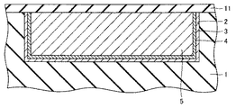
図1は、本発明の実施の形態1における半導体装置の構造を示す断面図である。
図2〜図10は、本発明の実施の形態1における半導体装置の製造方法を工程順に示す断面図である。
図11は、本発明の実施の形態2における半導体装置の構造を示す断面図である。
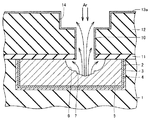
本実施の形態の半導体装置の製造方法において、導電膜15aを形成する際に、下部配線5を貫通するまで物理的にエッチングする。
図12は、本発明の実施の形態3における半導体装置の構造を示す断面図である。
図14は、本発明の実施の形態4における半導体装置の構造を示す断面図である。図14を参照して、本実施の形態の半導体装置は、以下の点において実施の形態1の半導体装置と異なっている。すなわち、Cu膜19を覆うように層間絶縁膜12上にライナー膜111が形成されており、ライナー膜111上に層間絶縁膜112が形成されている。層間絶縁膜112の上部にはトレンチ114が形成されており、トレンチ114内およびライナー膜111には、配線5aの上面29に達する孔110が開口されている。トレンチ114の内壁面および底部と、孔110の内壁面および底部とに沿って、バリアメタル113が形成されている。トレンチ114および孔110内を埋めるようにCu膜119が形成されている。
図15は、本発明の実施の形態5における半導体装置の断面を簡略化して示す図である。図15を参照して、本実施の形態の半導体装置は、多数の配線35a〜35fの各々と、配線35a〜35fの各々の間を電気的に接続するためのコンタクト39a〜39eの各々とを備えている。配線35a〜35fの各々は、絶縁層を介してこの順序で積層して形成されている。また、配線35aおよび配線35bはコンタクト39aによって電気的に接続されており、配線35bおよび配線35cはコンタクト39bによって電気的に接続されている。また、配線35cおよび配線35dはコンタクト39cによって電気的に接続されており、配線35dおよび配線35eはコンタクト39dによって電気的に接続されている。さらに、配線35eおよび配線35fはコンタクト39eによって電気的に接続されている。
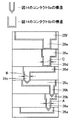
図17は、本発明の実施の形態6における半導体装置の断面を簡略化して示す図である。図17を参照して、コンタクト39a〜39eは口径Aまたは口径Cを有している。コンタクト39a〜39cの各々は口径Aを有しており、コンタクト39dおよび39eの各々は口径Cを有している。口径Cは口径Aよりも大きい。
本実施例では、従来の半導体装置と本発明の半導体装置との信頼性を比較した。具体的には、下部配線をエッチングせずにビアホールを形成した従来の半導体装置と、図1に示す本発明の半導体装置との寿命を調べた。図18にその結果を示す。なお、従来の半導体装置については、図18中の黒丸と白丸との2つの集団についての寿命を調べた。四角は本発明の半導体装置を示している。
Claims (10)
- 半導体基板上に形成され、第一層間絶縁膜と上記第一層間絶縁膜内に第一銅配線とを有する第一層と、
上記第一層上に形成され、上記第一銅配線の上面に接するように形成される第一絶縁膜と、
上記第一絶縁膜上に形成された第二層間絶縁膜と、
上記第一銅配線の上方において上記第一絶縁膜を貫通するように上記第二層間絶縁膜及び上記第一絶縁膜に設けられた第一ホールと、
上記第一ホールの側壁に沿って上記第二層間絶縁膜上及び上記第一絶縁膜上に形成された第一バリアメタルと、
上記第一ホールの下側に上記第一ホールと連通するように上記第一銅配線に設けられ、上記第一ホールの口径よりも大きな口径を有する第二ホールと、
上記第二ホールの下側に上記第二ホールと連通するように上記第一銅配線に設けられた、円錐形状又は半球形状の第三ホールと、
上記第二ホールの内壁面に形成された所定の導電膜と、
上記第一バリアメタル上、上記第二ホール内の上記所定の導電膜上及び上記第三ホールの内壁面に形成された第二バリアメタルと、
上記第一、第二及び第三ホール内に埋め込まれた第一銅金属とを有することを特徴とする半導体装置。 - 半導体基板上に形成され、第一層間絶縁膜と上記第一層間絶縁膜内に第一銅配線とを有する第一層と、
上記第一層上に形成され、上記第一銅配線の上面に接するように形成される第一絶縁膜と、
上記第一絶縁膜上に形成された第二層間絶縁膜と、
上記第一銅配線の上方において上記第一絶縁膜を貫通するように上記第二層間絶縁膜及び上記第一絶縁膜に設けられた第一ホールと、
上記第一ホールの側壁に沿って上記第二層間絶縁膜上及び上記第一絶縁膜上に形成された第一バリアメタルと、
上記第一ホールの下側に上記第一ホールと連通するように上記第一銅配線に設けられ、上記第一ホールの口径よりも大きな口径を有する第二ホールと、
上記第二ホールの下側に上記第二ホールと連通するように上記第一銅配線に設けられ、上記第一銅配線を30nm以上掘り込むことで形成された第三ホールと、
上記第二ホールの内壁面に形成された所定の導電膜と、
上記第一バリアメタル上、上記第二ホール内の上記所定の導電膜上及び上記第三ホールの内壁面に形成された第二バリアメタルと、
上記第一、第二及び第三ホール内に埋め込まれた第一銅金属とを有することを特徴とする半導体装置。 - 半導体基板上に形成され、第一層間絶縁膜と上記第一層間絶縁膜内に第一銅配線とを有する第一層と、
上記第一層上に形成され、上記第一銅配線の上面に接するように形成される第一絶縁膜と、
上記第一絶縁膜上に形成された第二層間絶縁膜と、
上記第一銅配線の上方において上記第一絶縁膜を貫通するように上記第二層間絶縁膜及び上記第一絶縁膜に設けられた第一ホールと、
上記第一ホールの側壁に沿って上記第二層間絶縁膜上及び上記第一絶縁膜上に形成された第一バリアメタルと、
上記第一ホールの下側に上記第一ホールと連通するように上記第一銅配線に設けられ、上記第一ホールの口径よりも大きな口径を有する第二ホールと、
上記第二ホールの下側に上記第二ホールと連通するように上記第一銅配線に設けられ、上記第一ホールの口径よりも小さな口径を有する第三ホールと、
上記第二ホールの内壁面に形成された所定の導電膜と、
上記第一バリアメタル上、上記第二ホール内の上記所定の導電膜上及び上記第三ホールの内壁面に形成された第二バリアメタルと、
上記第一、第二及び第三ホール内に埋め込まれた第一銅金属とを有することを特徴とする半導体装置。 - 上記第二層間絶縁膜内に設けられた第一溝内に形成された第二銅配線を更に有し、
上記第一溝の底面及び側面の上記第二層間絶縁膜上に形成された第三バリアメタルと、上記第一溝内の第二銅金属により上記第二銅配線が形成され、
上記第一バリアメタル、上記第二バリアメタル及び上記第一銅金属により第一ビアが形成され、
上記第三バリアメタルと上記第二バリアメタルは同一工程で形成され、
上記第一銅金属及び上記第二銅金属は同一工程で形成されることを特徴とする請求項1〜3のいずれか一項に記載の半導体装置。 - 上記第一バリアメタルと上記第二バリアメタルとの間に、上記第一バリアメタルの材料と上記第一銅配線の材料との合金で構成された上記所定の導電膜を更に有することを特徴とする請求項4に記載の半導体装置。
- 上記第一層間絶縁膜及び上記第二層間絶縁膜はそれぞれ、TEOS、SiO2、SiO
Cから選択された一つの材料を含有し、
上記第一バリアメタル、上記第二バリアメタルおよび上記第三バリアメタルはそれぞれ、タンタル、タンタル窒化物、タンタル珪化物、タンタル炭化物、チタン窒化物、チタン珪化物、チタン炭化物、タングステン窒化物、タングステン珪化物、タングステン炭化物、ルテニウム、およびルテニウム酸化物よりなる群から選ばれる1種以上の膜より形成されていることを特徴とする請求項4に記載の半導体装置。 - 上記第一銅金属と上記第二銅金属はそれぞれ、シード層と上記シード層上に形成された銅層により構成されていることを特徴とする請求項4に記載の半導体装置。
- 上記第二銅配線上及び上記第二層間絶縁膜上に第二層がさらに形成されており、
上記第二層は、
上記第二銅配線上及び上記第二層間絶縁膜上に形成された第二絶縁膜と、
上記第二絶縁膜上に形成された第三層間絶縁膜と、
上記第二絶縁膜と上記第三層間絶縁膜を貫通するように設けられ、上記第二銅配線を露出するように設けられた第四ホールと、
上記第三層間絶縁膜内に形成され、上記第四ホールと連通する第二溝と、
上記第二溝の側面、上記第二溝の底面、上記第四ホールの側面及び上記第四ホールの底面に形成された第四バリアメタルと、
上記第四バリアメタル上に形成された第三銅金属とを有し、
上記第四ホール内の上記第四バリアメタルと上記第三銅金属により第二ビアが形成され、上記第二溝内の上記第四バリアメタルと上記第三銅金属により第三銅配線が形成され、
上記第四ホールの底面の上記第四バリアメタルは露出した上記第二銅配線と接触しており、
上記第四ホールの底面の上記第四バリアメタルは、上記第二絶縁膜と第二銅配線との接触面よりも高い位置に存在することを特徴とする請求項4に記載の半導体装置。 - 上記第四ホールの径よりも上記第一ホールの径の方が小さいことを特徴とする請求項8記載の半導体装置。
- 上記第一絶縁膜はSiCN、SiC又はSiCOのうちのいずれかを材料とすることを特徴とする請求項4記載の半導体装置。
Priority Applications (8)
| Application Number | Priority Date | Filing Date | Title |
|---|---|---|---|
| JP2005165252A JP4832807B2 (ja) | 2004-06-10 | 2005-06-06 | 半導体装置 |
| US11/148,307 US7192871B2 (en) | 2004-06-10 | 2005-06-09 | Semiconductor device with a line and method of fabrication thereof |
| US11/676,951 US7709955B2 (en) | 2004-06-10 | 2007-02-20 | Semiconductor device with a line and method of fabrication thereof |
| US11/676,962 US7709388B2 (en) | 2004-06-10 | 2007-02-20 | Semiconductor device with a line and method of fabrication thereof |
| US12/730,039 US7936069B2 (en) | 2004-06-10 | 2010-03-23 | Semiconductor device with a line and method of fabrication thereof |
| US13/052,712 US8222146B2 (en) | 2004-06-10 | 2011-03-21 | Semiconductor device with a line and method of fabrication thereof |
| US13/419,053 US8432037B2 (en) | 2004-06-10 | 2012-03-13 | Semiconductor device with a line and method of fabrication thereof |
| US13/867,733 US8749064B2 (en) | 2004-06-10 | 2013-04-22 | Semiconductor device with a line and method of fabrication thereof |
Applications Claiming Priority (3)
| Application Number | Priority Date | Filing Date | Title |
|---|---|---|---|
| JP2004172500 | 2004-06-10 | ||
| JP2004172500 | 2004-06-10 | ||
| JP2005165252A JP4832807B2 (ja) | 2004-06-10 | 2005-06-06 | 半導体装置 |
Related Child Applications (1)
| Application Number | Title | Priority Date | Filing Date |
|---|---|---|---|
| JP2008125029A Division JP4786680B2 (ja) | 2004-06-10 | 2008-05-12 | 半導体装置の製造方法 |
Publications (3)
| Publication Number | Publication Date |
|---|---|
| JP2006024905A JP2006024905A (ja) | 2006-01-26 |
| JP2006024905A5 JP2006024905A5 (ja) | 2008-06-26 |
| JP4832807B2 true JP4832807B2 (ja) | 2011-12-07 |
Family
ID=35459691
Family Applications (1)
| Application Number | Title | Priority Date | Filing Date |
|---|---|---|---|
| JP2005165252A Active JP4832807B2 (ja) | 2004-06-10 | 2005-06-06 | 半導体装置 |
Country Status (2)
| Country | Link |
|---|---|
| US (5) | US7192871B2 (ja) |
| JP (1) | JP4832807B2 (ja) |
Cited By (1)
| Publication number | Priority date | Publication date | Assignee | Title |
|---|---|---|---|---|
| US9553121B2 (en) | 2014-08-28 | 2017-01-24 | Renesas Electronics Corporation | Semiconductor device and method of manufacturing the same |
Families Citing this family (43)
| Publication number | Priority date | Publication date | Assignee | Title |
|---|---|---|---|---|
| US6764940B1 (en) | 2001-03-13 | 2004-07-20 | Novellus Systems, Inc. | Method for depositing a diffusion barrier for copper interconnect applications |
| US7842605B1 (en) * | 2003-04-11 | 2010-11-30 | Novellus Systems, Inc. | Atomic layer profiling of diffusion barrier and metal seed layers |
| US8298933B2 (en) * | 2003-04-11 | 2012-10-30 | Novellus Systems, Inc. | Conformal films on semiconductor substrates |
| JP4786680B2 (ja) * | 2004-06-10 | 2011-10-05 | ルネサスエレクトロニクス株式会社 | 半導体装置の製造方法 |
| US8432037B2 (en) | 2004-06-10 | 2013-04-30 | Renesas Electronics Corporation | Semiconductor device with a line and method of fabrication thereof |
| JP4832807B2 (ja) | 2004-06-10 | 2011-12-07 | ルネサスエレクトロニクス株式会社 | 半導体装置 |
| US20060009030A1 (en) * | 2004-07-08 | 2006-01-12 | Texas Instruments Incorporated | Novel barrier integration scheme for high-reliability vias |
| DE102005024914A1 (de) * | 2005-05-31 | 2006-12-07 | Advanced Micro Devices, Inc., Sunnyvale | Verfahren zum Ausbilden elektrisch leitfähiger Leitungen in einem integrierten Schaltkreis |
| US7727888B2 (en) * | 2005-08-31 | 2010-06-01 | International Business Machines Corporation | Interconnect structure and method for forming the same |
| JP2007109736A (ja) * | 2005-10-11 | 2007-04-26 | Nec Electronics Corp | 半導体装置およびその製造方法 |
| JP2007109894A (ja) * | 2005-10-13 | 2007-04-26 | Matsushita Electric Ind Co Ltd | 半導体装置及びその製造方法 |
| JP2007180407A (ja) * | 2005-12-28 | 2007-07-12 | Matsushita Electric Ind Co Ltd | 半導体装置およびその製造方法 |
| JP5014632B2 (ja) * | 2006-01-13 | 2012-08-29 | ルネサスエレクトロニクス株式会社 | 半導体装置および半導体装置の製造方法 |
| US7528066B2 (en) * | 2006-03-01 | 2009-05-05 | International Business Machines Corporation | Structure and method for metal integration |
| DE102006035645B4 (de) * | 2006-07-31 | 2012-03-08 | Advanced Micro Devices, Inc. | Verfahren zum Ausbilden einer elektrisch leitfähigen Leitung in einem integrierten Schaltkreis |
| US7510634B1 (en) | 2006-11-10 | 2009-03-31 | Novellus Systems, Inc. | Apparatus and methods for deposition and/or etch selectivity |
| US20080128907A1 (en) * | 2006-12-01 | 2008-06-05 | International Business Machines Corporation | Semiconductor structure with liner |
| JP5154789B2 (ja) * | 2006-12-21 | 2013-02-27 | ルネサスエレクトロニクス株式会社 | 半導体装置並びに半導体装置の製造方法 |
| KR100790452B1 (ko) * | 2006-12-28 | 2008-01-03 | 주식회사 하이닉스반도체 | 다마신 공정을 이용한 반도체 소자의 다층 금속배선형성방법 |
| US7682966B1 (en) | 2007-02-01 | 2010-03-23 | Novellus Systems, Inc. | Multistep method of depositing metal seed layers |
| JP5127251B2 (ja) * | 2007-02-01 | 2013-01-23 | パナソニック株式会社 | 半導体装置の製造方法 |
| US7859113B2 (en) * | 2007-02-27 | 2010-12-28 | International Business Machines Corporation | Structure including via having refractory metal collar at copper wire and dielectric layer liner-less interface and related method |
| US8030778B2 (en) * | 2007-07-06 | 2011-10-04 | United Microelectronics Corp. | Integrated circuit structure and manufacturing method thereof |
| JP2009049178A (ja) * | 2007-08-20 | 2009-03-05 | Rohm Co Ltd | 半導体装置 |
| US8354751B2 (en) * | 2008-06-16 | 2013-01-15 | International Business Machines Corporation | Interconnect structure for electromigration enhancement |
| US7951708B2 (en) * | 2009-06-03 | 2011-05-31 | International Business Machines Corporation | Copper interconnect structure with amorphous tantalum iridium diffusion barrier |
| JP5754209B2 (ja) * | 2011-03-31 | 2015-07-29 | 大日本印刷株式会社 | 半導体装置の製造方法 |
| US8791014B2 (en) * | 2012-03-16 | 2014-07-29 | Globalfoundries Inc. | Methods of forming copper-based conductive structures on semiconductor devices |
| US9842765B2 (en) * | 2015-03-16 | 2017-12-12 | Taiwan Semiconductor Manufacturing Co., Ltd. | Semiconductor device structure and method for forming the same |
| US10170358B2 (en) * | 2015-06-04 | 2019-01-01 | International Business Machines Corporation | Reducing contact resistance in vias for copper interconnects |
| US10153351B2 (en) * | 2016-01-29 | 2018-12-11 | Taiwan Semiconductor Manufacturing Co., Ltd. | Semiconductor device and a method for fabricating the same |
| CN107564850B (zh) * | 2016-07-01 | 2020-07-07 | 中芯国际集成电路制造(北京)有限公司 | 互连结构及其制造方法 |
| JP6934726B2 (ja) * | 2017-01-27 | 2021-09-15 | Sppテクノロジーズ株式会社 | スパッタエッチング用マスク、スパッタエッチング方法及びスパッタエッチング装置 |
| CN107104120B (zh) * | 2017-05-24 | 2019-03-15 | 成都线易科技有限责任公司 | 磁感应器件及制造方法 |
| US10249534B2 (en) * | 2017-05-30 | 2019-04-02 | Globalfoundries Inc. | Method of forming a contact element of a semiconductor device and contact element structure |
| US10818545B2 (en) * | 2018-06-29 | 2020-10-27 | Sandisk Technologies Llc | Contact via structure including a barrier metal disc for low resistance contact and methods of making the same |
| CN110797298A (zh) * | 2018-08-03 | 2020-02-14 | 群创光电股份有限公司 | 电子装置及其制备方法 |
| US10685876B2 (en) * | 2018-09-18 | 2020-06-16 | International Business Machines Corporation | Liner and cap structures for reducing local interconnect vertical resistance without compromising reliability |
| US11121025B2 (en) * | 2018-09-27 | 2021-09-14 | Taiwan Semiconductor Manufacturing Company, Ltd. | Layer for side wall passivation |
| CN110718504B (zh) * | 2019-09-02 | 2022-07-29 | 长江存储科技有限责任公司 | 插塞结构、三维存储器的形成方法和三维存储器 |
| KR20210036113A (ko) | 2019-09-25 | 2021-04-02 | 삼성전자주식회사 | 반도체 장치 및 이의 제조 방법 |
| US11424185B2 (en) | 2019-12-30 | 2022-08-23 | Taiwan Semiconductor Manufacturing Co., Ltd. | Semiconductor device and manufacturing method thereof |
| US20220336269A1 (en) * | 2021-04-15 | 2022-10-20 | Taiwan Semiconductor Manufacturing Company, Ltd. | Homogeneous source/drain contact structure |
Family Cites Families (25)
| Publication number | Priority date | Publication date | Assignee | Title |
|---|---|---|---|---|
| US1109955A (en) * | 1914-03-06 | 1914-09-08 | Arthur C Barrett | Expansion-bolt. |
| JPH0714836A (ja) | 1993-06-17 | 1995-01-17 | Kawasaki Steel Corp | 多層配線構造の半導体装置 |
| JP3027951B2 (ja) * | 1997-03-12 | 2000-04-04 | 日本電気株式会社 | 半導体装置の製造方法 |
| JP3660799B2 (ja) * | 1997-09-08 | 2005-06-15 | 株式会社ルネサステクノロジ | 半導体集積回路装置の製造方法 |
| JP2000012684A (ja) * | 1998-06-18 | 2000-01-14 | Sony Corp | 金属層の形成方法 |
| US6287977B1 (en) | 1998-07-31 | 2001-09-11 | Applied Materials, Inc. | Method and apparatus for forming improved metal interconnects |
| JP3317279B2 (ja) | 1998-08-17 | 2002-08-26 | セイコーエプソン株式会社 | 半導体装置の製造方法 |
| JP2000114261A (ja) | 1998-10-02 | 2000-04-21 | Seiko Epson Corp | 半導体装置とその製造方法 |
| JP2001077195A (ja) | 1999-09-07 | 2001-03-23 | Sony Corp | 半導体装置 |
| JP2002064138A (ja) | 2000-08-18 | 2002-02-28 | Hitachi Ltd | 半導体集積回路装置およびその製造方法 |
| JP2002064139A (ja) * | 2000-08-18 | 2002-02-28 | Hitachi Ltd | 半導体装置の製造方法 |
| US6498091B1 (en) * | 2000-11-01 | 2002-12-24 | Applied Materials, Inc. | Method of using a barrier sputter reactor to remove an underlying barrier layer |
| US6436814B1 (en) * | 2000-11-21 | 2002-08-20 | International Business Machines Corporation | Interconnection structure and method for fabricating same |
| US6613664B2 (en) * | 2000-12-28 | 2003-09-02 | Infineon Technologies Ag | Barbed vias for electrical and mechanical connection between conductive layers in semiconductor devices |
| KR100385227B1 (ko) * | 2001-02-12 | 2003-05-27 | 삼성전자주식회사 | 구리 다층 배선을 가지는 반도체 장치 및 그 형성방법 |
| US6607977B1 (en) * | 2001-03-13 | 2003-08-19 | Novellus Systems, Inc. | Method of depositing a diffusion barrier for copper interconnect applications |
| JP2002299436A (ja) * | 2001-03-29 | 2002-10-11 | Toshiba Corp | 半導体装置およびその製造方法 |
| JP2003249547A (ja) * | 2002-02-22 | 2003-09-05 | Mitsubishi Electric Corp | 配線間の接続構造及びその製造方法 |
| US20030203615A1 (en) * | 2002-04-25 | 2003-10-30 | Denning Dean J. | Method for depositing barrier layers in an opening |
| US6949461B2 (en) | 2002-12-11 | 2005-09-27 | International Business Machines Corporation | Method for depositing a metal layer on a semiconductor interconnect structure |
| JP2004342702A (ja) * | 2003-05-13 | 2004-12-02 | Nec Electronics Corp | 半導体装置及び半導体装置の製造方法 |
| JP2005050903A (ja) * | 2003-07-30 | 2005-02-24 | Toshiba Corp | 半導体装置およびその製造方法 |
| JP4278481B2 (ja) * | 2003-10-23 | 2009-06-17 | 株式会社ルネサステクノロジ | 半導体装置の製造方法 |
| US20050173799A1 (en) * | 2004-02-05 | 2005-08-11 | Taiwan Semiconductor Manufacturing Co., Ltd. | Interconnect structure and method for its fabricating |
| JP4832807B2 (ja) | 2004-06-10 | 2011-12-07 | ルネサスエレクトロニクス株式会社 | 半導体装置 |
-
2005
- 2005-06-06 JP JP2005165252A patent/JP4832807B2/ja active Active
- 2005-06-09 US US11/148,307 patent/US7192871B2/en active Active
-
2007
- 2007-02-20 US US11/676,951 patent/US7709955B2/en active Active
- 2007-02-20 US US11/676,962 patent/US7709388B2/en active Active
-
2010
- 2010-03-23 US US12/730,039 patent/US7936069B2/en active Active
-
2011
- 2011-03-21 US US13/052,712 patent/US8222146B2/en not_active Expired - Fee Related
Cited By (1)
| Publication number | Priority date | Publication date | Assignee | Title |
|---|---|---|---|---|
| US9553121B2 (en) | 2014-08-28 | 2017-01-24 | Renesas Electronics Corporation | Semiconductor device and method of manufacturing the same |
Also Published As
| Publication number | Publication date |
|---|---|
| JP2006024905A (ja) | 2006-01-26 |
| US20070141831A1 (en) | 2007-06-21 |
| US20110171828A1 (en) | 2011-07-14 |
| US7709955B2 (en) | 2010-05-04 |
| US20050275110A1 (en) | 2005-12-15 |
| US20070138532A1 (en) | 2007-06-21 |
| US7936069B2 (en) | 2011-05-03 |
| US20100176511A1 (en) | 2010-07-15 |
| US7709388B2 (en) | 2010-05-04 |
| US7192871B2 (en) | 2007-03-20 |
| US8222146B2 (en) | 2012-07-17 |
Similar Documents
| Publication | Publication Date | Title |
|---|---|---|
| JP4832807B2 (ja) | 半導体装置 | |
| US7514354B2 (en) | Methods for forming damascene wiring structures having line and plug conductors formed from different materials | |
| TWI402936B (zh) | 用於金屬集成之新穎結構及其製造方法 | |
| JP4918778B2 (ja) | 半導体集積回路装置の製造方法 | |
| US7439624B2 (en) | Enhanced mechanical strength via contacts | |
| US8749064B2 (en) | Semiconductor device with a line and method of fabrication thereof | |
| US8466055B2 (en) | Semiconductor device and method of manufacturing semiconductor device | |
| US20070059919A1 (en) | Method of manufacturing semiconductor device | |
| JP4764606B2 (ja) | 半導体装置およびその製造方法 | |
| JP2010258215A (ja) | 半導体装置及び半導体装置の製造方法 | |
| JP2009026989A (ja) | 半導体装置及び半導体装置の製造方法 | |
| KR100660915B1 (ko) | 반도체 소자의 배선 형성 방법 | |
| CN110707066A (zh) | 一种内连线结构及其制备方法 | |
| JP2007294625A (ja) | 半導体装置の製造方法 | |
| JP2007115980A (ja) | 半導体装置及びその製造方法 | |
| JP2010507236A (ja) | 半導体デバイスおよび相互接続構造体の形成方法 | |
| KR101141214B1 (ko) | 반도체 소자의 금속 배선 형성 방법 | |
| JP4786680B2 (ja) | 半導体装置の製造方法 | |
| JP2007335578A (ja) | 半導体装置及びその製造方法 | |
| JP5310721B2 (ja) | 半導体装置とその製造方法 | |
| JP2007194566A (ja) | 半導体装置およびその製造方法 | |
| KR100720402B1 (ko) | 듀얼 다마센 공정을 이용한 금속 배선 형성 방법 | |
| US7727885B2 (en) | Reduction of punch-thru defects in damascene processing | |
| JP2009170665A (ja) | 半導体装置および半導体装置の製造方法 | |
| KR20100073779A (ko) | 반도체 소자의 금속배선 및 그 제조 방법 |
Legal Events
| Date | Code | Title | Description |
|---|---|---|---|
| A521 | Request for written amendment filed |
Free format text: JAPANESE INTERMEDIATE CODE: A523 Effective date: 20080512 |
|
| A621 | Written request for application examination |
Free format text: JAPANESE INTERMEDIATE CODE: A621 Effective date: 20080512 |
|
| A977 | Report on retrieval |
Free format text: JAPANESE INTERMEDIATE CODE: A971007 Effective date: 20100331 |
|
| A131 | Notification of reasons for refusal |
Free format text: JAPANESE INTERMEDIATE CODE: A131 Effective date: 20100511 |
|
| A711 | Notification of change in applicant |
Free format text: JAPANESE INTERMEDIATE CODE: A712 Effective date: 20100518 |
|
| A521 | Request for written amendment filed |
Free format text: JAPANESE INTERMEDIATE CODE: A523 Effective date: 20100712 |
|
| A131 | Notification of reasons for refusal |
Free format text: JAPANESE INTERMEDIATE CODE: A131 Effective date: 20110628 |
|
| A521 | Request for written amendment filed |
Free format text: JAPANESE INTERMEDIATE CODE: A523 Effective date: 20110822 |
|
| TRDD | Decision of grant or rejection written | ||
| A01 | Written decision to grant a patent or to grant a registration (utility model) |
Free format text: JAPANESE INTERMEDIATE CODE: A01 Effective date: 20110913 |
|
| A01 | Written decision to grant a patent or to grant a registration (utility model) |
Free format text: JAPANESE INTERMEDIATE CODE: A01 |
|
| A61 | First payment of annual fees (during grant procedure) |
Free format text: JAPANESE INTERMEDIATE CODE: A61 Effective date: 20110921 |
|
| R150 | Certificate of patent or registration of utility model |
Ref document number: 4832807 Country of ref document: JP Free format text: JAPANESE INTERMEDIATE CODE: R150 Free format text: JAPANESE INTERMEDIATE CODE: R150 |
|
| FPAY | Renewal fee payment (event date is renewal date of database) |
Free format text: PAYMENT UNTIL: 20140930 Year of fee payment: 3 |
|
| S531 | Written request for registration of change of domicile |
Free format text: JAPANESE INTERMEDIATE CODE: R313531 |
|
| R350 | Written notification of registration of transfer |
Free format text: JAPANESE INTERMEDIATE CODE: R350 |