JP4014591B2 - 半導体装置および電子機器 - Google Patents
半導体装置および電子機器 Download PDFInfo
- Publication number
- JP4014591B2 JP4014591B2 JP2004292435A JP2004292435A JP4014591B2 JP 4014591 B2 JP4014591 B2 JP 4014591B2 JP 2004292435 A JP2004292435 A JP 2004292435A JP 2004292435 A JP2004292435 A JP 2004292435A JP 4014591 B2 JP4014591 B2 JP 4014591B2
- Authority
- JP
- Japan
- Prior art keywords
- semiconductor device
- insulating film
- wiring
- semiconductor
- heat
- Prior art date
- Legal status (The legal status is an assumption and is not a legal conclusion. Google has not performed a legal analysis and makes no representation as to the accuracy of the status listed.)
- Expired - Lifetime
Links
Images


Classifications
-
- H—ELECTRICITY
- H05—ELECTRIC TECHNIQUES NOT OTHERWISE PROVIDED FOR
- H05K—PRINTED CIRCUITS; CASINGS OR CONSTRUCTIONAL DETAILS OF ELECTRIC APPARATUS; MANUFACTURE OF ASSEMBLAGES OF ELECTRICAL COMPONENTS
- H05K1/00—Printed circuits
- H05K1/02—Details
- H05K1/0201—Thermal arrangements, e.g. for cooling, heating or preventing overheating
- H05K1/0203—Cooling of mounted components
- H05K1/0209—External configuration of printed circuit board adapted for heat dissipation, e.g. lay-out of conductors, coatings
-
- H—ELECTRICITY
- H10—SEMICONDUCTOR DEVICES; ELECTRIC SOLID-STATE DEVICES NOT OTHERWISE PROVIDED FOR
- H10W—GENERIC PACKAGES, INTERCONNECTIONS, CONNECTORS OR OTHER CONSTRUCTIONAL DETAILS OF DEVICES COVERED BY CLASS H10
- H10W70/00—Package substrates; Interposers; Redistribution layers [RDL]
- H10W70/60—Insulating or insulated package substrates; Interposers; Redistribution layers
-
- H—ELECTRICITY
- H10—SEMICONDUCTOR DEVICES; ELECTRIC SOLID-STATE DEVICES NOT OTHERWISE PROVIDED FOR
- H10W—GENERIC PACKAGES, INTERCONNECTIONS, CONNECTORS OR OTHER CONSTRUCTIONAL DETAILS OF DEVICES COVERED BY CLASS H10
- H10W40/00—Arrangements for thermal protection or thermal control
- H10W40/10—Arrangements for heating
-
- H—ELECTRICITY
- H05—ELECTRIC TECHNIQUES NOT OTHERWISE PROVIDED FOR
- H05K—PRINTED CIRCUITS; CASINGS OR CONSTRUCTIONAL DETAILS OF ELECTRIC APPARATUS; MANUFACTURE OF ASSEMBLAGES OF ELECTRICAL COMPONENTS
- H05K1/00—Printed circuits
- H05K1/18—Printed circuits structurally associated with non-printed electric components
- H05K1/189—Printed circuits structurally associated with non-printed electric components characterised by the use of flexible or folded printed circuits
-
- H—ELECTRICITY
- H05—ELECTRIC TECHNIQUES NOT OTHERWISE PROVIDED FOR
- H05K—PRINTED CIRCUITS; CASINGS OR CONSTRUCTIONAL DETAILS OF ELECTRIC APPARATUS; MANUFACTURE OF ASSEMBLAGES OF ELECTRICAL COMPONENTS
- H05K2201/00—Indexing scheme relating to printed circuits covered by H05K1/00
- H05K2201/03—Conductive materials
- H05K2201/0332—Structure of the conductor
- H05K2201/0388—Other aspects of conductors
- H05K2201/0394—Conductor crossing over a hole in the substrate or a gap between two separate substrate parts
-
- H—ELECTRICITY
- H05—ELECTRIC TECHNIQUES NOT OTHERWISE PROVIDED FOR
- H05K—PRINTED CIRCUITS; CASINGS OR CONSTRUCTIONAL DETAILS OF ELECTRIC APPARATUS; MANUFACTURE OF ASSEMBLAGES OF ELECTRICAL COMPONENTS
- H05K2201/00—Indexing scheme relating to printed circuits covered by H05K1/00
- H05K2201/03—Conductive materials
- H05K2201/0332—Structure of the conductor
- H05K2201/0388—Other aspects of conductors
- H05K2201/0397—Tab
-
- H—ELECTRICITY
- H05—ELECTRIC TECHNIQUES NOT OTHERWISE PROVIDED FOR
- H05K—PRINTED CIRCUITS; CASINGS OR CONSTRUCTIONAL DETAILS OF ELECTRIC APPARATUS; MANUFACTURE OF ASSEMBLAGES OF ELECTRICAL COMPONENTS
- H05K2201/00—Indexing scheme relating to printed circuits covered by H05K1/00
- H05K2201/09—Shape and layout
- H05K2201/09209—Shape and layout details of conductors
- H05K2201/09654—Shape and layout details of conductors covering at least two types of conductors provided for in H05K2201/09218 - H05K2201/095
- H05K2201/09781—Dummy conductors, i.e. not used for normal transport of current; Dummy electrodes of components
-
- H—ELECTRICITY
- H05—ELECTRIC TECHNIQUES NOT OTHERWISE PROVIDED FOR
- H05K—PRINTED CIRCUITS; CASINGS OR CONSTRUCTIONAL DETAILS OF ELECTRIC APPARATUS; MANUFACTURE OF ASSEMBLAGES OF ELECTRICAL COMPONENTS
- H05K2201/00—Indexing scheme relating to printed circuits covered by H05K1/00
- H05K2201/10—Details of components or other objects attached to or integrated in a printed circuit board
- H05K2201/10613—Details of electrical connections of non-printed components, e.g. special leads
- H05K2201/10621—Components characterised by their electrical contacts
- H05K2201/10674—Flip chip
-
- H—ELECTRICITY
- H05—ELECTRIC TECHNIQUES NOT OTHERWISE PROVIDED FOR
- H05K—PRINTED CIRCUITS; CASINGS OR CONSTRUCTIONAL DETAILS OF ELECTRIC APPARATUS; MANUFACTURE OF ASSEMBLAGES OF ELECTRICAL COMPONENTS
- H05K2201/00—Indexing scheme relating to printed circuits covered by H05K1/00
- H05K2201/20—Details of printed circuits not provided for in H05K2201/01 - H05K2201/10
- H05K2201/2009—Reinforced areas, e.g. for a specific part of a flexible printed circuit
-
- H—ELECTRICITY
- H05—ELECTRIC TECHNIQUES NOT OTHERWISE PROVIDED FOR
- H05K—PRINTED CIRCUITS; CASINGS OR CONSTRUCTIONAL DETAILS OF ELECTRIC APPARATUS; MANUFACTURE OF ASSEMBLAGES OF ELECTRICAL COMPONENTS
- H05K3/00—Apparatus or processes for manufacturing printed circuits
- H05K3/0058—Laminating printed circuit boards onto other substrates, e.g. metallic substrates
- H05K3/0061—Laminating printed circuit boards onto other substrates, e.g. metallic substrates onto a metallic substrate, e.g. a heat sink
-
- H—ELECTRICITY
- H05—ELECTRIC TECHNIQUES NOT OTHERWISE PROVIDED FOR
- H05K—PRINTED CIRCUITS; CASINGS OR CONSTRUCTIONAL DETAILS OF ELECTRIC APPARATUS; MANUFACTURE OF ASSEMBLAGES OF ELECTRICAL COMPONENTS
- H05K3/00—Apparatus or processes for manufacturing printed circuits
- H05K3/40—Forming printed elements for providing electric connections to or between printed circuits
- H05K3/4038—Through-connections; Vertical interconnect access [VIA] connections
- H05K3/4084—Through-connections; Vertical interconnect access [VIA] connections by deforming at least one of the conductive layers
-
- H—ELECTRICITY
- H10—SEMICONDUCTOR DEVICES; ELECTRIC SOLID-STATE DEVICES NOT OTHERWISE PROVIDED FOR
- H10W—GENERIC PACKAGES, INTERCONNECTIONS, CONNECTORS OR OTHER CONSTRUCTIONAL DETAILS OF DEVICES COVERED BY CLASS H10
- H10W72/00—Interconnections or connectors in packages
- H10W72/071—Connecting or disconnecting
- H10W72/072—Connecting or disconnecting of bump connectors
- H10W72/07251—Connecting or disconnecting of bump connectors characterised by changes in properties of the bump connectors during connecting
-
- H—ELECTRICITY
- H10—SEMICONDUCTOR DEVICES; ELECTRIC SOLID-STATE DEVICES NOT OTHERWISE PROVIDED FOR
- H10W—GENERIC PACKAGES, INTERCONNECTIONS, CONNECTORS OR OTHER CONSTRUCTIONAL DETAILS OF DEVICES COVERED BY CLASS H10
- H10W72/00—Interconnections or connectors in packages
- H10W72/071—Connecting or disconnecting
- H10W72/073—Connecting or disconnecting of die-attach connectors
-
- H—ELECTRICITY
- H10—SEMICONDUCTOR DEVICES; ELECTRIC SOLID-STATE DEVICES NOT OTHERWISE PROVIDED FOR
- H10W—GENERIC PACKAGES, INTERCONNECTIONS, CONNECTORS OR OTHER CONSTRUCTIONAL DETAILS OF DEVICES COVERED BY CLASS H10
- H10W72/00—Interconnections or connectors in packages
- H10W72/20—Bump connectors, e.g. solder bumps or copper pillars; Dummy bumps; Thermal bumps
-
- H—ELECTRICITY
- H10—SEMICONDUCTOR DEVICES; ELECTRIC SOLID-STATE DEVICES NOT OTHERWISE PROVIDED FOR
- H10W—GENERIC PACKAGES, INTERCONNECTIONS, CONNECTORS OR OTHER CONSTRUCTIONAL DETAILS OF DEVICES COVERED BY CLASS H10
- H10W74/00—Encapsulations, e.g. protective coatings
- H10W74/01—Manufacture or treatment
- H10W74/012—Manufacture or treatment of encapsulations on active surfaces of flip-chip devices, e.g. forming underfills
-
- H—ELECTRICITY
- H10—SEMICONDUCTOR DEVICES; ELECTRIC SOLID-STATE DEVICES NOT OTHERWISE PROVIDED FOR
- H10W—GENERIC PACKAGES, INTERCONNECTIONS, CONNECTORS OR OTHER CONSTRUCTIONAL DETAILS OF DEVICES COVERED BY CLASS H10
- H10W74/00—Encapsulations, e.g. protective coatings
- H10W74/10—Encapsulations, e.g. protective coatings characterised by their shape or disposition
- H10W74/15—Encapsulations, e.g. protective coatings characterised by their shape or disposition on active surfaces of flip-chip devices, e.g. underfills
-
- H—ELECTRICITY
- H10—SEMICONDUCTOR DEVICES; ELECTRIC SOLID-STATE DEVICES NOT OTHERWISE PROVIDED FOR
- H10W—GENERIC PACKAGES, INTERCONNECTIONS, CONNECTORS OR OTHER CONSTRUCTIONAL DETAILS OF DEVICES COVERED BY CLASS H10
- H10W90/00—Package configurations
- H10W90/701—Package configurations characterised by the relative positions of pads or connectors relative to package parts
- H10W90/721—Package configurations characterised by the relative positions of pads or connectors relative to package parts of bump connectors
- H10W90/724—Package configurations characterised by the relative positions of pads or connectors relative to package parts of bump connectors between a chip and a stacked insulating package substrate, interposer or RDL
-
- H—ELECTRICITY
- H10—SEMICONDUCTOR DEVICES; ELECTRIC SOLID-STATE DEVICES NOT OTHERWISE PROVIDED FOR
- H10W—GENERIC PACKAGES, INTERCONNECTIONS, CONNECTORS OR OTHER CONSTRUCTIONAL DETAILS OF DEVICES COVERED BY CLASS H10
- H10W90/00—Package configurations
- H10W90/701—Package configurations characterised by the relative positions of pads or connectors relative to package parts
- H10W90/731—Package configurations characterised by the relative positions of pads or connectors relative to package parts of die-attach connectors
- H10W90/734—Package configurations characterised by the relative positions of pads or connectors relative to package parts of die-attach connectors between a chip and a stacked insulating package substrate, interposer or RDL
Landscapes
- Engineering & Computer Science (AREA)
- Microelectronics & Electronic Packaging (AREA)
- Cooling Or The Like Of Semiconductors Or Solid State Devices (AREA)
- Wire Bonding (AREA)
Description
絶縁フィルムと、
この絶縁フィルムの一方の面上に配置された配線と、
上記絶縁フィルムの上記一方の面に対向するように配置された一つまたは複数の半導体素子と、
上記絶縁体フィルムの他方の面上に配置された放熱部材と
を備え、
上記放熱部材は、上記絶縁体フィルムの上記他方の面における上記半導体素子に対応する箇所に、少なくとも配置され、
上記放熱部材は、上記絶縁フィルムの上記他方の面上に直接配置されていることを特徴としている。
また、一実施形態の半導体装置は、上記放熱部材が、放熱板であり、上記放熱板の上記絶縁フィルム側の面の表面積は、上記絶縁フィルムの上記放熱板側の面の表面積よりも大きくなっている。
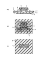
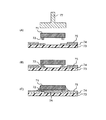
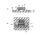
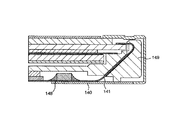
図1は、本発明の第1実施形態の半導体装置を示す図である。詳細には、図1(A)は、第1実施形態の半導体装置の断面図であり、図1(B)は、第1実施形態の半導体装置における半導体素子の搭載面を示す図であり、図1(C)は、第1実施形態の半導体装置の半導体素子が搭載されていない側の面を示す図である。
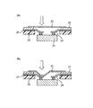
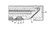
図3は、第2実施形態の半導体装置を示す図である。詳細には、図3(A)は、第2実施形態の半導体装置の断面図であり、図3(B)は、第1実施形態の半導体装置における半導体素子の搭載面と反対側の面を示す図である。
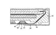
図4は、第3実施形態の半導体装置の絶縁フィルム43の半導体素子側と反対側の面を示す図である。
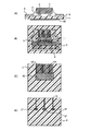
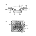
図5は、第4実施形態の半導体装置を示す図である。詳細には、図5(A)は、第4実施形態の半導体装置の断面図であり、図5(B)は、第4実施形態の半導体装置の半導体素子側の上面図であり、図5(C)は、第4実施形態の半導体装置の半導体素子側と反対側の上面図である。
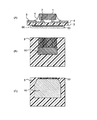
図6は、第5実施形態の半導体装置を示す図である。詳細には、図6(A)は、第5実施形態の半導体装置の断面図であり、図6(B)は、第5実施形態の半導体装置の製造途中の絶縁フィルムにおける半導体素子側と反対側の表面を示す図である。また、図6(C)は、第5実施形態の半導体装置の絶縁フィルムにおける半導体素子側と反対側の表面を示す図である。
2,72 バンプ電極
3,73 絶縁フィルム
4,74 配線
5,75 ソルダーレジスト
6,76 封止樹脂
10,30,40,50,57 放熱板
66 樹脂薄膜
80,90 半導体装置
Claims (14)
- 絶縁フィルムと、
この絶縁フィルムの一方の面上に配置された配線と、
上記絶縁フィルムの上記一方の面に対向するように配置された一つまたは複数の半導体素子と、
上記絶縁体フィルムの他方の面上に配置された放熱部材と
を備え、
上記放熱部材は、上記絶縁体フィルムの上記他方の面における上記半導体素子に対応する箇所に、少なくとも配置され、
上記放熱部材は、上記絶縁フィルムの上記他方の面上に直接配置されていることを特徴とする半導体装置。 - 請求項1に記載の半導体装置において、
上記放熱部材は、上記絶縁体フィルムの上記他方の面における上記配線に対応する箇所に、少なくとも配置されていることを特徴とする半導体装置。 - 請求項1に記載の半導体装置において、
上記放熱部材は、互いに連続していない複数の部分から成ることを特徴とする半導体装置。 - 請求項1に記載の半導体装置において、
上記半導体素子は、少なくとも2種類の半導体素子を含むことを特徴とする半導体装置。 - 請求項1に記載の半導体装置において、
上記半導体素子のバンプ電極と、上記配線とは、Au−Snの合金接合によって接続されていることを特徴とする半導体装置。 - 請求項1に記載の半導体装置において、
上記半導体素子のバンプ電極と、上記配線とは、Au−Auの合金接合によって接続されていることを特徴とする半導体装置。 - 請求項1に記載の半導体装置において、
上記半導体素子のバンプ電極と、上記配線とは、異方性導電接着フィルムによって接続されていることを特徴とする半導体装置。 - 請求項1に記載の半導体装置において、
上記半導体素子のバンプ電極と、上記配線とは、異方性導電接着ペーストによって接続されていることを特徴とする半導体装置。 - 請求項1に記載の半導体装置において、
上記半導体素子のバンプ電極と、上記配線とは、非導電性接着ペーストによって接続されていることを特徴とする半導体装置。 - 請求項1に記載の半導体装置において、
上記半導体素子のバンプ電極と、上記配線とは、非導電性接着フィルムによって接続されていることを特徴とする半導体装置。 - 請求項1に記載の半導体装置において、
上記絶縁フィルムの上に、受動素子を配置していることを特徴とする半導体装置。 - 請求項1に記載の半導体装置において、
上記放熱部材の表面の一部または表面の全面に、絶縁性の薄膜樹脂が塗布されるか、または、上記放熱部材の表面の一部または表面の全面に、絶縁性のシート部材が貼り付けられていることを特徴とする半導体装置。 - 請求項1に記載の半導体装置において、
上記放熱部材は、放熱板であり、
上記放熱板の上記絶縁フィルム側の面の表面積は、上記絶縁フィルムの上記放熱板側の面の表面積よりも大きいことを特徴とする半導体装置。 - 請求項1に記載の半導体装置と、放熱用部品とを備える電子機器であって、
上記半導体装置の放熱部材と、上記放熱用部品とは、直接的に連結されていることを特徴とする電子機器。
Priority Applications (5)
| Application Number | Priority Date | Filing Date | Title |
|---|---|---|---|
| JP2004292435A JP4014591B2 (ja) | 2004-10-05 | 2004-10-05 | 半導体装置および電子機器 |
| CNB2005101291378A CN100385648C (zh) | 2004-10-05 | 2005-09-30 | 半导体器件以及电子设备 |
| KR1020050092674A KR20060051982A (ko) | 2004-10-05 | 2005-10-01 | 반도체 장치 및 전자기기 |
| US11/241,972 US20060071325A1 (en) | 2004-10-05 | 2005-10-04 | Semiconductor device and electronic apparatus |
| TW094134686A TWI302736B (en) | 2004-10-05 | 2005-10-04 | Semiconductor device and electronic apparatus |
Applications Claiming Priority (1)
| Application Number | Priority Date | Filing Date | Title |
|---|---|---|---|
| JP2004292435A JP4014591B2 (ja) | 2004-10-05 | 2004-10-05 | 半導体装置および電子機器 |
Publications (2)
| Publication Number | Publication Date |
|---|---|
| JP2006108356A JP2006108356A (ja) | 2006-04-20 |
| JP4014591B2 true JP4014591B2 (ja) | 2007-11-28 |
Family
ID=36124726
Family Applications (1)
| Application Number | Title | Priority Date | Filing Date |
|---|---|---|---|
| JP2004292435A Expired - Lifetime JP4014591B2 (ja) | 2004-10-05 | 2004-10-05 | 半導体装置および電子機器 |
Country Status (5)
| Country | Link |
|---|---|
| US (1) | US20060071325A1 (ja) |
| JP (1) | JP4014591B2 (ja) |
| KR (1) | KR20060051982A (ja) |
| CN (1) | CN100385648C (ja) |
| TW (1) | TWI302736B (ja) |
Families Citing this family (22)
| Publication number | Priority date | Publication date | Assignee | Title |
|---|---|---|---|---|
| KR101144557B1 (ko) * | 2006-03-27 | 2012-05-11 | 엘지이노텍 주식회사 | 발광 다이오드 조명장치 및 그 제조방법 |
| JP5489394B2 (ja) * | 2006-07-20 | 2014-05-14 | 三星電子株式会社 | Cof型半導体パッケージ |
| KR100785950B1 (ko) * | 2006-11-09 | 2007-12-14 | 스테코 주식회사 | Cof 패키지 및 그의 제조 방법 |
| JP5096782B2 (ja) * | 2007-04-19 | 2012-12-12 | ルネサスエレクトロニクス株式会社 | 半導体装置 |
| JP4109707B1 (ja) * | 2007-05-30 | 2008-07-02 | 新藤電子工業株式会社 | 半導体装置およびその製造方法、ならびにディスプレイ装置およびその製造方法 |
| KR101493869B1 (ko) | 2008-04-17 | 2015-02-23 | 삼성전자주식회사 | 방열 부재 테이프, 방열부재를 구비한 씨오에프(cof)형 반도체 패키지 및 이를 적용한 전자장치 |
| JP5095460B2 (ja) * | 2008-01-17 | 2012-12-12 | シャープ株式会社 | 半導体装置および表示装置 |
| JP5184115B2 (ja) * | 2008-01-31 | 2013-04-17 | 日東電工株式会社 | 配線回路基板およびその製造方法 |
| JP5238274B2 (ja) * | 2008-01-31 | 2013-07-17 | 日東電工株式会社 | 配線回路基板およびその製造方法 |
| DE102008016899A1 (de) * | 2008-04-02 | 2009-10-22 | Continental Automotive Gmbh | Elektrisches Gerät |
| JP4981744B2 (ja) | 2008-05-09 | 2012-07-25 | 日東電工株式会社 | 配線回路基板およびその製造方法 |
| JP5236377B2 (ja) * | 2008-07-16 | 2013-07-17 | シャープ株式会社 | 半導体装置および表示装置 |
| DE102010039146A1 (de) * | 2010-08-10 | 2012-02-16 | Robert Bosch Gmbh | Verfahren zum elektrisch leitenden Verbinden von Leiterbahnen in Leitungsträgern und System umfassend solche Leitungsträger |
| JP6176817B2 (ja) | 2011-10-17 | 2017-08-09 | ローム株式会社 | チップダイオードおよびダイオードパッケージ |
| JP6389300B2 (ja) * | 2011-10-17 | 2018-09-12 | ローム株式会社 | 半導体装置 |
| KR101981173B1 (ko) * | 2012-10-16 | 2019-05-23 | 삼성디스플레이 주식회사 | 표시 장치용 본딩 장치 및 그 방법 |
| US10032969B2 (en) * | 2014-12-26 | 2018-07-24 | Nichia Corporation | Light emitting device |
| US10043737B2 (en) | 2015-12-02 | 2018-08-07 | Novatek Microelectronics Corp. | Chip on film package |
| US9978663B2 (en) | 2015-12-09 | 2018-05-22 | Samsung Display Co., Ltd. | Integrated circuit assembly with heat spreader and method of making the same |
| DE102016220065A1 (de) * | 2016-10-14 | 2018-04-19 | Robert Bosch Gmbh | Verfahren zum Ausbilden mindestens eines Wärmeableitpfades für ein mikroelektronisches Bauteil und entsprechendes mikroelektronisches Bauteil |
| RS64565B1 (sr) * | 2018-12-07 | 2023-10-31 | Continental Automotive Tech Gmbh | Merenje temperature i ambijentalnog svetla kod tehnologija prikaza sa samostalnim osvetljenjem u primenama kod automobila |
| JP6924974B1 (ja) * | 2020-03-10 | 2021-08-25 | パナソニックIpマネジメント株式会社 | 撮像装置 |
Family Cites Families (31)
| Publication number | Priority date | Publication date | Assignee | Title |
|---|---|---|---|---|
| JPS61144098A (ja) * | 1984-12-18 | 1986-07-01 | 三菱電線工業株式会社 | 片側面絶縁型回路用基板の製造方法 |
| JPH0310224A (ja) * | 1989-06-07 | 1991-01-17 | Sharp Corp | 表示装置 |
| US5616520A (en) * | 1992-03-30 | 1997-04-01 | Hitachi, Ltd. | Semiconductor integrated circuit device and fabrication method thereof |
| US5583378A (en) * | 1994-05-16 | 1996-12-10 | Amkor Electronics, Inc. | Ball grid array integrated circuit package with thermal conductor |
| JP2944449B2 (ja) * | 1995-02-24 | 1999-09-06 | 日本電気株式会社 | 半導体パッケージとその製造方法 |
| US5739584A (en) * | 1995-06-07 | 1998-04-14 | Lsi Logic Corporation | Multiple pin die package |
| US5796165A (en) * | 1996-03-19 | 1998-08-18 | Matsushita Electronics Corporation | High-frequency integrated circuit device having a multilayer structure |
| JP2806357B2 (ja) * | 1996-04-18 | 1998-09-30 | 日本電気株式会社 | スタックモジュール |
| JPH10163386A (ja) * | 1996-12-03 | 1998-06-19 | Toshiba Corp | 半導体装置、半導体パッケージおよび実装回路装置 |
| US5942795A (en) * | 1997-07-03 | 1999-08-24 | National Semiconductor Corporation | Leaded substrate carrier for integrated circuit device and leaded substrate carrier device assembly |
| US5901041A (en) * | 1997-12-02 | 1999-05-04 | Northern Telecom Limited | Flexible integrated circuit package |
| JP3859340B2 (ja) * | 1998-01-06 | 2006-12-20 | 三菱電機株式会社 | 半導体装置 |
| JPH11214435A (ja) * | 1998-01-26 | 1999-08-06 | Sharp Corp | 半導体装置およびその製造方法 |
| US6362530B1 (en) * | 1998-04-06 | 2002-03-26 | National Semiconductor Corporation | Manufacturing methods and construction for integrated circuit packages |
| US5939783A (en) * | 1998-05-05 | 1999-08-17 | International Business Machines Corporation | Electronic package |
| JP3147087B2 (ja) * | 1998-06-17 | 2001-03-19 | 日本電気株式会社 | 積層型半導体装置放熱構造 |
| US5854507A (en) * | 1998-07-21 | 1998-12-29 | Hewlett-Packard Company | Multiple chip assembly |
| US6219238B1 (en) * | 1999-05-10 | 2001-04-17 | International Business Machines Corporation | Structure for removably attaching a heat sink to surface mount packages |
| JP2000353770A (ja) * | 1999-05-20 | 2000-12-19 | Whitaker Corp:The | 集積回路パッケージ、ミリ波集積回路パッケージ、及び集積回路パッケージを基板に組立及び実装する方法 |
| TW561799B (en) * | 1999-08-11 | 2003-11-11 | Fujikura Ltd | Chip assembly module of bump connection type using a multi-layer printed circuit substrate |
| JP2001077236A (ja) * | 1999-09-07 | 2001-03-23 | Casio Comput Co Ltd | 半導体装置及びその接合構造 |
| US6677664B2 (en) * | 2000-04-25 | 2004-01-13 | Fujitsu Hitachi Plasma Display Limited | Display driver integrated circuit and flexible wiring board using a flat panel display metal chassis |
| US6512675B1 (en) * | 2000-06-28 | 2003-01-28 | Advanced Micro Devices, Inc. | Heat sink grounded to a grounded package lid |
| JP2002076215A (ja) * | 2000-08-29 | 2002-03-15 | Sony Corp | 半導体装置パッケージ及びその作製方法 |
| US6611055B1 (en) * | 2000-11-15 | 2003-08-26 | Skyworks Solutions, Inc. | Leadless flip chip carrier design and structure |
| US7259448B2 (en) * | 2001-05-07 | 2007-08-21 | Broadcom Corporation | Die-up ball grid array package with a heat spreader and method for making the same |
| JP4067802B2 (ja) * | 2001-09-18 | 2008-03-26 | 松下電器産業株式会社 | 照明装置 |
| JP3878527B2 (ja) * | 2002-08-20 | 2007-02-07 | 住友電工プリントサーキット株式会社 | プリント基板 |
| JP2004214249A (ja) * | 2002-12-27 | 2004-07-29 | Renesas Technology Corp | 半導体モジュール |
| US7095053B2 (en) * | 2003-05-05 | 2006-08-22 | Lamina Ceramics, Inc. | Light emitting diodes packaged for high temperature operation |
| TWI300261B (en) * | 2003-07-02 | 2008-08-21 | Advanced Semiconductor Eng | Chip package structur |
-
2004
- 2004-10-05 JP JP2004292435A patent/JP4014591B2/ja not_active Expired - Lifetime
-
2005
- 2005-09-30 CN CNB2005101291378A patent/CN100385648C/zh not_active Expired - Lifetime
- 2005-10-01 KR KR1020050092674A patent/KR20060051982A/ko not_active Ceased
- 2005-10-04 TW TW094134686A patent/TWI302736B/zh not_active IP Right Cessation
- 2005-10-04 US US11/241,972 patent/US20060071325A1/en not_active Abandoned
Also Published As
| Publication number | Publication date |
|---|---|
| CN100385648C (zh) | 2008-04-30 |
| KR20060051982A (ko) | 2006-05-19 |
| TWI302736B (en) | 2008-11-01 |
| CN1767177A (zh) | 2006-05-03 |
| US20060071325A1 (en) | 2006-04-06 |
| TW200629524A (en) | 2006-08-16 |
| JP2006108356A (ja) | 2006-04-20 |
Similar Documents
| Publication | Publication Date | Title |
|---|---|---|
| JP4014591B2 (ja) | 半導体装置および電子機器 | |
| US9633919B2 (en) | Package structure with an elastomer with lower elastic modulus | |
| US20140029201A1 (en) | Power package module and manufacturing method thereof | |
| JP5582995B2 (ja) | ソケット | |
| JP2008091714A (ja) | 半導体装置 | |
| JP2006073651A (ja) | 半導体装置 | |
| KR102674888B1 (ko) | 인쇄회로기판 조립체 | |
| JPWO2018216627A1 (ja) | 電子機器 | |
| TW201417642A (zh) | 連接基板及層疊封裝結構 | |
| KR100768998B1 (ko) | 다층인쇄회로기판을 사용한 범프접속형 칩실장모듈 | |
| US20100271785A1 (en) | Heat-dissipating and fixing mechanism of electronic component and process for assembling same | |
| JP5169800B2 (ja) | 電子装置 | |
| JP4975584B2 (ja) | 半導体装置及び半導体装置の製造方法。 | |
| JP2005012127A (ja) | 電子制御装置 | |
| JP2013065887A (ja) | 電子装置 | |
| CN1331228C (zh) | 混合型模块 | |
| JP6928129B2 (ja) | 電力変換装置 | |
| JP7223639B2 (ja) | 電子制御装置 | |
| JP5003730B2 (ja) | 電子装置 | |
| JP5667023B2 (ja) | 集合配線基板および電子装置の実装方法 | |
| US7310224B2 (en) | Electronic apparatus with thermal module | |
| JP4193702B2 (ja) | 半導体パッケージの実装構造 | |
| JP4514530B2 (ja) | 精密機器に内蔵される回路モジュールおよび精密機器 | |
| JP2022057425A (ja) | パワーモジュール及びパワーモジュールの製造方法 | |
| JP2003007914A (ja) | 半導体装置 |
Legal Events
| Date | Code | Title | Description |
|---|---|---|---|
| A977 | Report on retrieval |
Free format text: JAPANESE INTERMEDIATE CODE: A971007 Effective date: 20070412 |
|
| A131 | Notification of reasons for refusal |
Free format text: JAPANESE INTERMEDIATE CODE: A131 Effective date: 20070508 |
|
| A521 | Request for written amendment filed |
Free format text: JAPANESE INTERMEDIATE CODE: A523 Effective date: 20070709 |
|
| TRDD | Decision of grant or rejection written | ||
| A01 | Written decision to grant a patent or to grant a registration (utility model) |
Free format text: JAPANESE INTERMEDIATE CODE: A01 Effective date: 20070904 |
|
| A61 | First payment of annual fees (during grant procedure) |
Free format text: JAPANESE INTERMEDIATE CODE: A61 Effective date: 20070911 |
|
| FPAY | Renewal fee payment (event date is renewal date of database) |
Free format text: PAYMENT UNTIL: 20100921 Year of fee payment: 3 |
|
| R150 | Certificate of patent or registration of utility model |
Ref document number: 4014591 Country of ref document: JP Free format text: JAPANESE INTERMEDIATE CODE: R150 Free format text: JAPANESE INTERMEDIATE CODE: R150 |
|
| FPAY | Renewal fee payment (event date is renewal date of database) |
Free format text: PAYMENT UNTIL: 20110921 Year of fee payment: 4 |
|
| FPAY | Renewal fee payment (event date is renewal date of database) |
Free format text: PAYMENT UNTIL: 20120921 Year of fee payment: 5 |
|
| FPAY | Renewal fee payment (event date is renewal date of database) |
Free format text: PAYMENT UNTIL: 20130921 Year of fee payment: 6 |
|
| R250 | Receipt of annual fees |
Free format text: JAPANESE INTERMEDIATE CODE: R250 |
|
| S531 | Written request for registration of change of domicile |
Free format text: JAPANESE INTERMEDIATE CODE: R313531 |
|
| S111 | Request for change of ownership or part of ownership |
Free format text: JAPANESE INTERMEDIATE CODE: R313113 |
|
| R350 | Written notification of registration of transfer |
Free format text: JAPANESE INTERMEDIATE CODE: R350 |
|
| R350 | Written notification of registration of transfer |
Free format text: JAPANESE INTERMEDIATE CODE: R350 |
|
| R250 | Receipt of annual fees |
Free format text: JAPANESE INTERMEDIATE CODE: R250 |
|
| R250 | Receipt of annual fees |
Free format text: JAPANESE INTERMEDIATE CODE: R250 |
|
| R250 | Receipt of annual fees |
Free format text: JAPANESE INTERMEDIATE CODE: R250 |
|
| R250 | Receipt of annual fees |
Free format text: JAPANESE INTERMEDIATE CODE: R250 |
|
| EXPY | Cancellation because of completion of term |