JP3966614B2 - Wide viewing angle LCD - Google Patents
Wide viewing angle LCD Download PDFInfo
- Publication number
- JP3966614B2 JP3966614B2 JP14721398A JP14721398A JP3966614B2 JP 3966614 B2 JP3966614 B2 JP 3966614B2 JP 14721398 A JP14721398 A JP 14721398A JP 14721398 A JP14721398 A JP 14721398A JP 3966614 B2 JP3966614 B2 JP 3966614B2
- Authority
- JP
- Japan
- Prior art keywords
- liquid crystal
- display device
- crystal display
- substrate
- opening
- Prior art date
- Legal status (The legal status is an assumption and is not a legal conclusion. Google has not performed a legal analysis and makes no representation as to the accuracy of the status listed.)
- Expired - Lifetime
Links
Images


Classifications
-
- G—PHYSICS
- G02—OPTICS
- G02F—OPTICAL DEVICES OR ARRANGEMENTS FOR THE CONTROL OF LIGHT BY MODIFICATION OF THE OPTICAL PROPERTIES OF THE MEDIA OF THE ELEMENTS INVOLVED THEREIN; NON-LINEAR OPTICS; FREQUENCY-CHANGING OF LIGHT; OPTICAL LOGIC ELEMENTS; OPTICAL ANALOGUE/DIGITAL CONVERTERS
- G02F1/00—Devices or arrangements for the control of the intensity, colour, phase, polarisation or direction of light arriving from an independent light source, e.g. switching, gating or modulating; Non-linear optics
- G02F1/01—Devices or arrangements for the control of the intensity, colour, phase, polarisation or direction of light arriving from an independent light source, e.g. switching, gating or modulating; Non-linear optics for the control of the intensity, phase, polarisation or colour
- G02F1/13—Devices or arrangements for the control of the intensity, colour, phase, polarisation or direction of light arriving from an independent light source, e.g. switching, gating or modulating; Non-linear optics for the control of the intensity, phase, polarisation or colour based on liquid crystals, e.g. single liquid crystal display cells
- G02F1/137—Devices or arrangements for the control of the intensity, colour, phase, polarisation or direction of light arriving from an independent light source, e.g. switching, gating or modulating; Non-linear optics for the control of the intensity, phase, polarisation or colour based on liquid crystals, e.g. single liquid crystal display cells characterised by the electro-optical or magneto-optical effect, e.g. field-induced phase transition, orientation effect, guest-host interaction or dynamic scattering
-
- G—PHYSICS
- G02—OPTICS
- G02F—OPTICAL DEVICES OR ARRANGEMENTS FOR THE CONTROL OF LIGHT BY MODIFICATION OF THE OPTICAL PROPERTIES OF THE MEDIA OF THE ELEMENTS INVOLVED THEREIN; NON-LINEAR OPTICS; FREQUENCY-CHANGING OF LIGHT; OPTICAL LOGIC ELEMENTS; OPTICAL ANALOGUE/DIGITAL CONVERTERS
- G02F1/00—Devices or arrangements for the control of the intensity, colour, phase, polarisation or direction of light arriving from an independent light source, e.g. switching, gating or modulating; Non-linear optics
- G02F1/01—Devices or arrangements for the control of the intensity, colour, phase, polarisation or direction of light arriving from an independent light source, e.g. switching, gating or modulating; Non-linear optics for the control of the intensity, phase, polarisation or colour
- G02F1/13—Devices or arrangements for the control of the intensity, colour, phase, polarisation or direction of light arriving from an independent light source, e.g. switching, gating or modulating; Non-linear optics for the control of the intensity, phase, polarisation or colour based on liquid crystals, e.g. single liquid crystal display cells
- G02F1/133—Constructional arrangements; Operation of liquid crystal cells; Circuit arrangements
- G02F1/1333—Constructional arrangements; Manufacturing methods
- G02F1/1337—Surface-induced orientation of the liquid crystal molecules, e.g. by alignment layers
- G02F1/133707—Structures for producing distorted electric fields, e.g. bumps, protrusions, recesses, slits in pixel electrodes
-
- G—PHYSICS
- G02—OPTICS
- G02F—OPTICAL DEVICES OR ARRANGEMENTS FOR THE CONTROL OF LIGHT BY MODIFICATION OF THE OPTICAL PROPERTIES OF THE MEDIA OF THE ELEMENTS INVOLVED THEREIN; NON-LINEAR OPTICS; FREQUENCY-CHANGING OF LIGHT; OPTICAL LOGIC ELEMENTS; OPTICAL ANALOGUE/DIGITAL CONVERTERS
- G02F1/00—Devices or arrangements for the control of the intensity, colour, phase, polarisation or direction of light arriving from an independent light source, e.g. switching, gating or modulating; Non-linear optics
- G02F1/01—Devices or arrangements for the control of the intensity, colour, phase, polarisation or direction of light arriving from an independent light source, e.g. switching, gating or modulating; Non-linear optics for the control of the intensity, phase, polarisation or colour
- G02F1/13—Devices or arrangements for the control of the intensity, colour, phase, polarisation or direction of light arriving from an independent light source, e.g. switching, gating or modulating; Non-linear optics for the control of the intensity, phase, polarisation or colour based on liquid crystals, e.g. single liquid crystal display cells
- G02F1/133—Constructional arrangements; Operation of liquid crystal cells; Circuit arrangements
- G02F1/1333—Constructional arrangements; Manufacturing methods
- G02F1/1343—Electrodes
- G02F1/134309—Electrodes characterised by their geometrical arrangement
- G02F1/134336—Matrix
-
- G—PHYSICS
- G02—OPTICS
- G02F—OPTICAL DEVICES OR ARRANGEMENTS FOR THE CONTROL OF LIGHT BY MODIFICATION OF THE OPTICAL PROPERTIES OF THE MEDIA OF THE ELEMENTS INVOLVED THEREIN; NON-LINEAR OPTICS; FREQUENCY-CHANGING OF LIGHT; OPTICAL LOGIC ELEMENTS; OPTICAL ANALOGUE/DIGITAL CONVERTERS
- G02F1/00—Devices or arrangements for the control of the intensity, colour, phase, polarisation or direction of light arriving from an independent light source, e.g. switching, gating or modulating; Non-linear optics
- G02F1/01—Devices or arrangements for the control of the intensity, colour, phase, polarisation or direction of light arriving from an independent light source, e.g. switching, gating or modulating; Non-linear optics for the control of the intensity, phase, polarisation or colour
- G02F1/13—Devices or arrangements for the control of the intensity, colour, phase, polarisation or direction of light arriving from an independent light source, e.g. switching, gating or modulating; Non-linear optics for the control of the intensity, phase, polarisation or colour based on liquid crystals, e.g. single liquid crystal display cells
- G02F1/133—Constructional arrangements; Operation of liquid crystal cells; Circuit arrangements
- G02F1/136—Liquid crystal cells structurally associated with a semi-conducting layer or substrate, e.g. cells forming part of an integrated circuit
- G02F1/1362—Active matrix addressed cells
- G02F1/136213—Storage capacitors associated with the pixel electrode
-
- G—PHYSICS
- G02—OPTICS
- G02F—OPTICAL DEVICES OR ARRANGEMENTS FOR THE CONTROL OF LIGHT BY MODIFICATION OF THE OPTICAL PROPERTIES OF THE MEDIA OF THE ELEMENTS INVOLVED THEREIN; NON-LINEAR OPTICS; FREQUENCY-CHANGING OF LIGHT; OPTICAL LOGIC ELEMENTS; OPTICAL ANALOGUE/DIGITAL CONVERTERS
- G02F1/00—Devices or arrangements for the control of the intensity, colour, phase, polarisation or direction of light arriving from an independent light source, e.g. switching, gating or modulating; Non-linear optics
- G02F1/01—Devices or arrangements for the control of the intensity, colour, phase, polarisation or direction of light arriving from an independent light source, e.g. switching, gating or modulating; Non-linear optics for the control of the intensity, phase, polarisation or colour
- G02F1/13—Devices or arrangements for the control of the intensity, colour, phase, polarisation or direction of light arriving from an independent light source, e.g. switching, gating or modulating; Non-linear optics for the control of the intensity, phase, polarisation or colour based on liquid crystals, e.g. single liquid crystal display cells
- G02F1/137—Devices or arrangements for the control of the intensity, colour, phase, polarisation or direction of light arriving from an independent light source, e.g. switching, gating or modulating; Non-linear optics for the control of the intensity, phase, polarisation or colour based on liquid crystals, e.g. single liquid crystal display cells characterised by the electro-optical or magneto-optical effect, e.g. field-induced phase transition, orientation effect, guest-host interaction or dynamic scattering
- G02F1/139—Devices or arrangements for the control of the intensity, colour, phase, polarisation or direction of light arriving from an independent light source, e.g. switching, gating or modulating; Non-linear optics for the control of the intensity, phase, polarisation or colour based on liquid crystals, e.g. single liquid crystal display cells characterised by the electro-optical or magneto-optical effect, e.g. field-induced phase transition, orientation effect, guest-host interaction or dynamic scattering based on orientation effects in which the liquid crystal remains transparent
- G02F1/1393—Devices or arrangements for the control of the intensity, colour, phase, polarisation or direction of light arriving from an independent light source, e.g. switching, gating or modulating; Non-linear optics for the control of the intensity, phase, polarisation or colour based on liquid crystals, e.g. single liquid crystal display cells characterised by the electro-optical or magneto-optical effect, e.g. field-induced phase transition, orientation effect, guest-host interaction or dynamic scattering based on orientation effects in which the liquid crystal remains transparent the birefringence of the liquid crystal being electrically controlled, e.g. ECB-, DAP-, HAN-, PI-LC cells
-
- G—PHYSICS
- G02—OPTICS
- G02F—OPTICAL DEVICES OR ARRANGEMENTS FOR THE CONTROL OF LIGHT BY MODIFICATION OF THE OPTICAL PROPERTIES OF THE MEDIA OF THE ELEMENTS INVOLVED THEREIN; NON-LINEAR OPTICS; FREQUENCY-CHANGING OF LIGHT; OPTICAL LOGIC ELEMENTS; OPTICAL ANALOGUE/DIGITAL CONVERTERS
- G02F1/00—Devices or arrangements for the control of the intensity, colour, phase, polarisation or direction of light arriving from an independent light source, e.g. switching, gating or modulating; Non-linear optics
- G02F1/01—Devices or arrangements for the control of the intensity, colour, phase, polarisation or direction of light arriving from an independent light source, e.g. switching, gating or modulating; Non-linear optics for the control of the intensity, phase, polarisation or colour
- G02F1/13—Devices or arrangements for the control of the intensity, colour, phase, polarisation or direction of light arriving from an independent light source, e.g. switching, gating or modulating; Non-linear optics for the control of the intensity, phase, polarisation or colour based on liquid crystals, e.g. single liquid crystal display cells
- G02F1/133—Constructional arrangements; Operation of liquid crystal cells; Circuit arrangements
- G02F1/1333—Constructional arrangements; Manufacturing methods
- G02F1/1335—Structural association of cells with optical devices, e.g. polarisers or reflectors
- G02F1/133509—Filters, e.g. light shielding masks
- G02F1/133512—Light shielding layers, e.g. black matrix
-
- G—PHYSICS
- G02—OPTICS
- G02F—OPTICAL DEVICES OR ARRANGEMENTS FOR THE CONTROL OF LIGHT BY MODIFICATION OF THE OPTICAL PROPERTIES OF THE MEDIA OF THE ELEMENTS INVOLVED THEREIN; NON-LINEAR OPTICS; FREQUENCY-CHANGING OF LIGHT; OPTICAL LOGIC ELEMENTS; OPTICAL ANALOGUE/DIGITAL CONVERTERS
- G02F1/00—Devices or arrangements for the control of the intensity, colour, phase, polarisation or direction of light arriving from an independent light source, e.g. switching, gating or modulating; Non-linear optics
- G02F1/01—Devices or arrangements for the control of the intensity, colour, phase, polarisation or direction of light arriving from an independent light source, e.g. switching, gating or modulating; Non-linear optics for the control of the intensity, phase, polarisation or colour
- G02F1/13—Devices or arrangements for the control of the intensity, colour, phase, polarisation or direction of light arriving from an independent light source, e.g. switching, gating or modulating; Non-linear optics for the control of the intensity, phase, polarisation or colour based on liquid crystals, e.g. single liquid crystal display cells
- G02F1/133—Constructional arrangements; Operation of liquid crystal cells; Circuit arrangements
- G02F1/1333—Constructional arrangements; Manufacturing methods
- G02F1/1337—Surface-induced orientation of the liquid crystal molecules, e.g. by alignment layers
-
- G—PHYSICS
- G02—OPTICS
- G02F—OPTICAL DEVICES OR ARRANGEMENTS FOR THE CONTROL OF LIGHT BY MODIFICATION OF THE OPTICAL PROPERTIES OF THE MEDIA OF THE ELEMENTS INVOLVED THEREIN; NON-LINEAR OPTICS; FREQUENCY-CHANGING OF LIGHT; OPTICAL LOGIC ELEMENTS; OPTICAL ANALOGUE/DIGITAL CONVERTERS
- G02F1/00—Devices or arrangements for the control of the intensity, colour, phase, polarisation or direction of light arriving from an independent light source, e.g. switching, gating or modulating; Non-linear optics
- G02F1/01—Devices or arrangements for the control of the intensity, colour, phase, polarisation or direction of light arriving from an independent light source, e.g. switching, gating or modulating; Non-linear optics for the control of the intensity, phase, polarisation or colour
- G02F1/13—Devices or arrangements for the control of the intensity, colour, phase, polarisation or direction of light arriving from an independent light source, e.g. switching, gating or modulating; Non-linear optics for the control of the intensity, phase, polarisation or colour based on liquid crystals, e.g. single liquid crystal display cells
- G02F1/133—Constructional arrangements; Operation of liquid crystal cells; Circuit arrangements
- G02F1/1333—Constructional arrangements; Manufacturing methods
- G02F1/1343—Electrodes
- G02F1/134309—Electrodes characterised by their geometrical arrangement
- G02F1/134372—Electrodes characterised by their geometrical arrangement for fringe field switching [FFS] where the common electrode is not patterned
-
- G—PHYSICS
- G02—OPTICS
- G02F—OPTICAL DEVICES OR ARRANGEMENTS FOR THE CONTROL OF LIGHT BY MODIFICATION OF THE OPTICAL PROPERTIES OF THE MEDIA OF THE ELEMENTS INVOLVED THEREIN; NON-LINEAR OPTICS; FREQUENCY-CHANGING OF LIGHT; OPTICAL LOGIC ELEMENTS; OPTICAL ANALOGUE/DIGITAL CONVERTERS
- G02F1/00—Devices or arrangements for the control of the intensity, colour, phase, polarisation or direction of light arriving from an independent light source, e.g. switching, gating or modulating; Non-linear optics
- G02F1/01—Devices or arrangements for the control of the intensity, colour, phase, polarisation or direction of light arriving from an independent light source, e.g. switching, gating or modulating; Non-linear optics for the control of the intensity, phase, polarisation or colour
- G02F1/13—Devices or arrangements for the control of the intensity, colour, phase, polarisation or direction of light arriving from an independent light source, e.g. switching, gating or modulating; Non-linear optics for the control of the intensity, phase, polarisation or colour based on liquid crystals, e.g. single liquid crystal display cells
- G02F1/137—Devices or arrangements for the control of the intensity, colour, phase, polarisation or direction of light arriving from an independent light source, e.g. switching, gating or modulating; Non-linear optics for the control of the intensity, phase, polarisation or colour based on liquid crystals, e.g. single liquid crystal display cells characterised by the electro-optical or magneto-optical effect, e.g. field-induced phase transition, orientation effect, guest-host interaction or dynamic scattering
- G02F1/13712—Devices or arrangements for the control of the intensity, colour, phase, polarisation or direction of light arriving from an independent light source, e.g. switching, gating or modulating; Non-linear optics for the control of the intensity, phase, polarisation or colour based on liquid crystals, e.g. single liquid crystal display cells characterised by the electro-optical or magneto-optical effect, e.g. field-induced phase transition, orientation effect, guest-host interaction or dynamic scattering the liquid crystal having negative dielectric anisotropy
-
- G—PHYSICS
- G02—OPTICS
- G02F—OPTICAL DEVICES OR ARRANGEMENTS FOR THE CONTROL OF LIGHT BY MODIFICATION OF THE OPTICAL PROPERTIES OF THE MEDIA OF THE ELEMENTS INVOLVED THEREIN; NON-LINEAR OPTICS; FREQUENCY-CHANGING OF LIGHT; OPTICAL LOGIC ELEMENTS; OPTICAL ANALOGUE/DIGITAL CONVERTERS
- G02F2201/00—Constructional arrangements not provided for in groups G02F1/00 - G02F7/00
- G02F2201/12—Constructional arrangements not provided for in groups G02F1/00 - G02F7/00 electrode
- G02F2201/121—Constructional arrangements not provided for in groups G02F1/00 - G02F7/00 electrode common or background
-
- G—PHYSICS
- G02—OPTICS
- G02F—OPTICAL DEVICES OR ARRANGEMENTS FOR THE CONTROL OF LIGHT BY MODIFICATION OF THE OPTICAL PROPERTIES OF THE MEDIA OF THE ELEMENTS INVOLVED THEREIN; NON-LINEAR OPTICS; FREQUENCY-CHANGING OF LIGHT; OPTICAL LOGIC ELEMENTS; OPTICAL ANALOGUE/DIGITAL CONVERTERS
- G02F2201/00—Constructional arrangements not provided for in groups G02F1/00 - G02F7/00
- G02F2201/12—Constructional arrangements not provided for in groups G02F1/00 - G02F7/00 electrode
- G02F2201/128—Constructional arrangements not provided for in groups G02F1/00 - G02F7/00 electrode field shaping
Description
【0001】
【発明の属する技術分野】
本発明は、広視野角液晶表示装置に関する。
【0002】
【従来の技術】
一般に、液晶表示装置は2枚の基板間に液晶を注入し、ここに加える電場の強さを調節して光透過量を調節する構造からなる。
ツイスト・ネマチック(twisted-nematic ; TN)方式の液晶表示装置は、内側面に透明電極が形成されている一対の透明基板、2つの透明基板間の液晶物質及びそれぞれの透明基板の外側面に取付けられて光を偏光する2つの偏光板で構成される。電気場を印加しない状態においては、2つの基板間に詰められた液晶分子が基板に平行で一定のピッチ(pitch)を有して螺線状にねじられ、液晶分子の長軸方向が連続的に変化するねじれた構造を有する。かかる構造のツイスト・ネマチック方式の液晶表示装置では液晶分子の長軸と短軸の配列に従って視覚特性が決定される。
【0003】
しかし、かかるTN方式の液晶表示装置のうちでも、特にノーマリーブラックモード(normally black mode)である場合には、電気場が印加されない状態で入射する光が完全に遮断されないため、コントラスト比がよくない。
【0004】
このような問題点を改善するために、垂直配向されたツイスト・ネマチック(vertically-aligned twisted-nematic ; VATN)方式の液晶表示装置が、米国特許第3,914,022号で提案されており、“Eurodisplay1993,pp.158−159"においてもTakahashi等によって提案されている。
【0005】
垂直配向液晶表示装置における電気場が印加されていない状態の液晶分子は、2つの基板に対して垂直に配向されているため、ノーマリーブラックモードで十分に暗い状態を作る。
【0006】
しかし、前記方式は、視野角があまり広くないという問題点がある。
【0007】
一方、T.Yamamoto等はフリンジフィールド(fringe field)による垂直配向方式の単純マトリックス液晶表示装置を“SID1991,p.762−765"で発表し、Lienは“SID1992,p.33−35"で単純マトリックス多重領域垂直配向液晶表示装置が、オン(ON)状態での光透過率が低い問題点を解決するために、画素電極に開口部を形成する構造を提案した。
【0008】
しかし、Lienが提案した構造では、画素電極が開いた部分、すなわち、分割された画素領域の境界となる部分で、光が漏れる現象が現われる。
【0009】
【発明が解決しようとする課題】
本発明は、前記に鑑みてなされたもので、その目的は、広視野角を有する液晶表示装置を提供することにある。また、本発明の目的は、広視野角液晶表示装置における光漏れを防止することにある。
【0010】
【課題を解決するための手段】
本発明による液晶表示装置は、共通電極が形成されている第1基板と、前記共通電極に対応する位置に画素電極及びこれと重なる維持電極を有する第2基板とからなり、前記共通電極と前記画素電極のうちの1つに開口部が設けられており、前記維持電極は前記開口部に対応する位置に形成されている。
【0011】
この時、維持電極は開口部によって形成されるフリンジフィールドにより発生する光漏れを防止する役割を果たす。
【0012】
ここで、第1基板と前記第2基板との間には負の誘電率異方性を有する液晶物質が注入されており、この液晶物質はキラルネマチック液晶またはキラル添加剤が0.01−3.0wt%含有されているネマチック液晶である。
【0013】
そして、第1基板と前記第2基板は、液晶物質の分子軸を垂直に配向するための配向膜が形成されている。このような配向膜はラビング処理をしてもしなくても良い。
【0014】
なお、維持電極はゲート線と連結することができ、2つ以上を形成することもできる。
【0015】
開口部の幅は3−15μmであることが好ましく、開口部間の幅は8−50μmに形成することが好ましい。
【0016】
一方、視野角を拡張するために、隣り合う単位画素領域に形成される線形の開口部は、互いに異なる方向に、例えば、画素領域を単位にして横方向と縦方向を繰返すように形成する。このような配置を通して液晶分子が多様な方向にねじられるようにする。
【0017】
【発明の実施の形態】
以下、本発明を明確にするために、図面に基づいて本発明による垂直配向を利用した液晶表示装置の実施例についてより詳しく説明する。
【0018】
図1(A)及び(B)は、本発明の実施例による垂直配向を利用した液晶表示装置における、液晶分子の配列をブラックモード及びホワイトモードに分別して示した概念図であり、図2は、本発明の実施例による垂直配向を利用した液晶表示装置において開いた画素電極によって発生するフリンジフィールドによる液晶分子の配列を示した断面図である。
【0019】
図1(A)及び(B)に示すように、ガラス等からなる2つの基板1、2が向かい合っており、2つの基板1、2の内側面にはITO(indium tin oxide)等の透明導電物質からなる透明電極12、120及び配向膜14、140が順に形成されている。2つの基板1、2の間には、負の誘電率異方性を有するキラルネマチック液晶や左旋性または右旋性のキラル添加剤が0.01−3.0wt%添加されているネマチック液晶物質からなる液晶層100がある。それぞれの基板1、2の外側面には、液晶層100に入射する光および液晶層100を通過して出る光を偏光させる偏光板13、130がそれぞれ取付けられており、下部基板1に取付けられた偏光板13の偏光軸(A)は、上部基板2に取付けられた偏光板130の偏光軸(B)に対して90度の角をなしている。配向膜14はラビング処理してもしなくても良い。
【0020】
図1(A)は電界を印加しない場合を示すもので、液晶層100の液晶分子3は、配向膜14の配向力によって2つの基板1、2の表面に対して垂直方向に配列されている。
【0021】
この時、下部基板1に取付けられている偏光板13を通過した光は偏光方向が変わらずに液晶層100を通過する。次に、この光は、上部基板2に取付けられている偏光板130により遮断されてブラック状態を現す。
【0022】
図1(B)は、電界を十分に印加した場合を示すもので、液晶分子3は下部基板1から上部基板2に至るまで90度の角度をなすように螺線状にねじれているため、液晶分子3の長軸の方向が連続的に変化するツイスト構造を有する。ここで、2つの基板1、2に隣接した部分では、加えられた電気場による力よりは配向膜14の配向力が強いので、液晶分子3は垂直に配向されたもとの状態を維持する。
【0023】
この時、下部基板1に取付けられた偏光板13を通過して偏光された光は、液晶層100を通過しながらその偏光軸が液晶分子3の長軸方向のねじれに従って90度回転することになり、これによって、反対側の基板2に取付けられている偏光板13を通過するようになり、ホワイト状態となる。
【0024】
図2は、本発明の実施例による垂直配向を利用した液晶表示装置において視野角を補償するために提案された構造及び原理を示すものである。上部または下部基板1、2に形成されているITO電極4、5のうち、上部基板2の電極4の一部が開いている。電界を印加しない状態においては、図1(A)に示すように、液晶分子3は2つの基板1、2に垂直に配列された状態を維持するため、電極が開いていない時と同様にブラック状態を現す。電界を印加すると、大部分のところでは基板1、2に垂直である電気場が形成されるが、ITO電極4の開いた部分付近での電気場は2つの基板1、2に対して完全に垂直に形成されない。このように開いた部分付近で形成される歪んだ電気場をフリンジフィールド(fringe field)という。液晶が負の誘電率異方性を有するため、液晶分子3の配列方向は電気場の方向と垂直になろうとする。
【0025】
このようなフリンジフィールドによって、開いた部分付近の液晶分子3の長軸は、2つの基板1、2の表面に対して傾いた状態でねじれることになる。
【0026】
本発明の実施例による液晶表示装置は、薄膜トランジスタ基板及びカラーフィルタ基板からなる。薄膜トランジスタ基板には互いに交差する多数のゲート線とデータ線が形成されており、ゲート線とデータ線に定義される各領域を指す単位画素領域には画素電極及び薄膜トランジスタが形成されている。これに向かい合うカラーフィルタ基板には全面に共通電極が形成されており、薄膜トランジスタ基板の単位画素に対応する領域である単位画素領域を定義するブラックマトリックスが形成されている。
【0027】
本発明の第1乃至第4実施例では開口部が設けられた部分に維持電極を形成して光漏れを防止する構造を提示する。
【0028】
まず、図3乃至5を参考にして本発明の第1実施例について説明する。
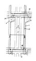
図3は本発明による液晶表示装置におけるカラーフィルタ基板を示した平面図である。 図3はカラーフィルタ基板の共通電極を単位画素領域別に開いた構造であって、1つの単位画素領域を示したものである。
【0029】
図3に示したように、1つの単位画素領域Pの境界にブラックマトリックス7のパターンが形成されており、共通電極6は全面に形成されている。この時、共通電極6には縦方向に2つの線形開口部15が互いに平行に形成されている。
【0030】
ここで、開口部15の幅は3−15μmの範囲であり、開口部15間の距離は8−50μmの範囲であることが好ましい。より好ましくは、開口部15の幅は3−12μmであり、開口部間の距離は10−30μmである。
【0031】
図4は本発明の第1実施例による液晶表示装置における薄膜トランジスタ基板を示した配置図であり、図5は図4のV−V′線により切断した断面図である。図4及び5に示したように、透明なガラス基板20の上に互いに平行な第1及び第2ゲート線81、82が横方向に形成されており、第1ゲート線81と第2ゲート線82とを連結する2つの維持電極11が縦方向に互いに平行に形成されている。この維持電極11はカラーフィルタ基板の共通電極6に形成されている開口部15に該当する位置に配置されて、フリンジフィールドによる光漏れを防止する役割を果たす。
【0032】
ゲート絶縁膜30が維持電極11と第1及び第2ゲート線81、82を覆っており、ゲート絶縁膜30の上部にはデータ線9が縦方向に形成されている。2つのゲート線81、82のうち、上部の第1ゲート線81とデータ線9とが交差する部分には薄膜トランジスタ(thin film transistor ; TFT)が形成されており、この上には平坦化された保護膜40が覆われている。保護膜40の上部には端部分が第1及び第2ゲート線82及びデータ線9と重なる画素電極10が形成されており、その上には画素電極10を覆う配向膜50が形成されている。ここで、配向膜50はラビング処理されていてもいなくても良い。
【0033】
共通電極に形成されている線形開口部は、横方向または傾いた方向に形成されることもできる。
【0034】
図6及び7は開口部が横方向に形成された本発明の第2実施例による構造を示している。
図6に示したように、1つの単位画素領域Pの境界にブラックマトリックス7のパターンが形成されており、共通電極6は全面に形成されている。ここで共通電極6に形成された開口部15は横方向に多数形成されている。
【0035】
ここで、開口部15の幅と開口部15間の距離は、開口部を縦方向に形成した本発明の第1実施例の場合と同様である。
【0036】
図7は本発明の第2実施例による液晶表示装置における薄膜トランジスタ基板を示した配置図である。
図7に示したように、互いに平行な第1及び第2ゲート線81、82が横方向に形成されており、画素領域Pには第1ゲート線81と第2ゲート線82とを連結する1つの分枝12が隣り合うデータ線9と平行に形成されており、多数の維持電極11がゲート線81、82と平行に分枝12から延長されている。この維持電極11は本発明の第1実施例と同様に、カラーフィルタ基板の共通電極6に形成されている開口部15に該当する位置に配置され、フリンジフィールドによる光漏れを防止する役割を果たす。
【0037】
図8乃至11は、開口部が斜線方向に形成された本発明の第3実施例及び第4実施例による構造を示している。
図8及び10に示したように、1つの単位画素領域Pの境界にブラックマトリックス7のパターンが形成されており、共通電極6は全面に形成されている。ここで、共通電極6に形成された開口部15は斜線方向に形成されている。図8に示した本発明の第3実施例の場合、画素の右上から左下に向う方向の開口部及び、画素の右下から左上に向う方向の開口部がそれぞれ1つずつ形成されている。図10に示したように本発明の第4実施例の場合には、2つの開口部が全て画素の右上から左下に向っており、互いに平行に形成されている。
【0038】
ここで、開口部15の幅と開口部15間の距離は、開口部を縦方向に形成した本発明の第1実施例の場合と同様である。
【0039】
図9及び11はそれぞれ、本発明の第3及び第4実施例による液晶表示装置における薄膜トランジスタを示した配置図である。
図9に示したように、互いに平行な第1及び第2ゲート線81、82が横方向に形成されており、画素領域Pには第1ゲート線81と第2ゲート線82とを連結する1つの分枝12が隣り合うデータ線9と平行に形成されており、2つの維持電極11が分枝のゲート線と隣接した下上部分から斜線方向に画素の中央部分に向って延長されている。図11に示した薄膜とトランジスタ基板も互いに平行な第1及び第2ゲート線81、82が横方向に形成されており、画素領域Pには第1ゲート線81と第2ゲート線82とを連結する1つの分枝12が隣り合うデータ線9と平行に形成されており、2つの維持電極11が右上から左下方向に互いに平行に形成されている。第3及び第4実施例において、この維持電極11は、本発明の第1実施例と同様にカラーフィルタ基板の共通電極6に形成されている開口部15に該当する位置に配置されて、フリンジフィールドによる光漏れを防止する役割を果たす。
【0040】
本発明の第3及び第4実施例で、画素電極の上に形成されている配向膜はラビングしてもしなくても良い。但し、ラビング処理をする場合には、ラビング方向は開口部の方向に対して0度から135度をなすことが好ましい。
【0041】
次に、本発明の第5実施例では、隣接した画素に形成される開口部の形状を異なるようにして視野角を拡張する構造を提示する。これを図12乃至15を参照して説明する。
【0042】
図12は本発明によるカラーフィルタ基板を示した図面である。
図12に示したように、赤、緑、青色のカラーフィルタに対応する多数の画素領域を定義するブラックマトリックス7のパターンが形成されており、線形の開口部15が形成されているITO電極4が形成されている。ここで、隣り合う画素領域の開口部15は互いに異なる方向に形成されている。すなわち、開口部15が画素を単位として横方向と縦方向に繰返されて形成されている。たとえば、赤色画素領域には開口部15が縦方向に形成されており、これと隣り合う緑色画素領域には開口部15が横方向に形成されている。
【0043】
このような構造で、画面に赤色を表示すると仮定する。そうすると、青色と緑色の画素はオフ(OFF)状態のままとなり、赤色の画素だけがオン(ON)状態となる。この時、隣接した赤色画素のITO電極4の開口部は、それぞれ横方向と縦方向に形成されている。この時の液晶分子の動きを図13(A)及び図13(B)を参考にして説明する。
【0044】
図13(A)では、ITO電極4の線形開口部15が縦方向に形成されており、図13(B)ではITO電極4の線形開口部15が横方向に形成されている。
【0045】
ここで、横方向をX軸、縦方向をY軸とすると、2つの電極4の間の液晶分子は、地面下部から見る時、左旋性液晶である。
【0046】
2つの電極4、5に電界が印加されると、液晶分子は形成される電気場の方向に垂直に傾くことになる。これと同時に、図13(A)では、開口部15がY軸に形成されて、Y軸上側に位置した液晶分子はX軸の右側に、Y軸下側に位置した液晶分子はX軸の左側の方向にそれぞれねじれる。また、図13(B)では、開口部15がX軸に形成されて、X軸右側に位置した液晶分子はY軸の下側の方向に、X軸左側に位置した液晶分子はY軸の上側にそれぞれねじれる。
【0047】
図13(A)及び図13(B)に示したように、4つの方向で液晶分子がねじれるため、上下左右方向の視野角が同一に形成され、階調反転も現れない。従って、全体に視野角が拡張する。
【0048】
次に、第5実施例によるカラーフィルタ基板及び薄膜トランジスタ基板の構造について詳細に説明する。
【0049】
図14はカラーフィルタ基板の共通電極を単位画素領域別に開いた構造であり、隣り合う2つの単位画素領域を示したものである。
図14に示したように、図3と同様にそれぞれの単位画素領域P1、P2を定義するブラックマトリックス7のパターンが形成されており、共通電極6は全面に形成されている。
【0050】
ここで画素領域P1の共通電極6には、縦方向に2つの線形開口部15が互いに平行に形成されており、これと隣り合う画素領域P2の共通電極6には横方向に多数の線形開口部15が互いに平行に形成されてている。
【0051】
ここで、開口部15の幅及びこれの間の距離は、第1実施例に従うことが好ましい。
【0052】
図15は本発明の第2実施例による薄膜トランジスタ基板の構造を示したもので、図12の画素領域P1に対応する画素領域P1には、図4と同様に第1ゲート線81と第2ゲート線82とを連結する2つの維持電極11が縦方向に互いに平行に形成されている。画素領域P2には、図7と同様に第1ゲート線81と第2ゲート線82とを連結する1つの分枝12が隣り合うデータ線9と平行に形成されており、多数の維持電極11がゲート線81、82と平行に分枝12から延長されている。
【0053】
前述の全ての実施例と同様に、維持電極11は、図14における共通電極6に形成されている開口部15に対応する位置に配置される。
【0054】
このような維持電極11は、画素電極10と重なって維持畜電器を形成する役割を果たすと同時に、共通電極6の開口部15によって形成されるディスクリネーション(disclination)によって漏れる光を遮断するブラックマトリックスの役割を果たす。
【0055】
隣り合う画素の開口部は、様々な形状に形成することができる。図16乃至19に、隣り合う画素の開口部を、異なる形状に形成した本発明の第6乃至第9実施例による液晶表示装置のカラーフィルタ基板の構造を示している。
【0056】
図16に示した本発明の第6実施例による液晶表示装置の構造は、図10に示した本発明の第4実施例による形状の開口部が形成された画素と、これを180度回転させた形状の画素とを横方向に交互に配置し、縦方向には同じ列に同じ形状の画素が配列されるように形成したものである。図17に示した本発明の第7実施例による液晶表示装置の構造は、横方向の配列は第7実施例と同様であるが、縦方向にも画素の形状が交互に繰返されるように配置したものである。図18に示した本発明の第8実施例による液晶表示装置の構造は、図8に示した本発明の第3実施例による形状に開口部が形成された画素と、これを180度回転させた形状の画素とを横方向に交互に配置し、縦方向には同じ列に同じ形状の画素が配列されるように形成したものである。図19に示した本発明の第9実施例による液晶表示装置の構造は、横方向の配列は第8実施例と同様であるが、縦方向にも画素の形状が交互に繰返されるように配置したものである。
【0057】
本発明の実施例による液晶表示装置では、球形の基板間隔材を用いる場合、基板間隔材による液晶配向の不良が生じて光漏れが発生する可能性があるので、金属や有機材料を利用した柱状の基板間隔材を使用することが好ましい。
【0058】
図20は、本発明の実施例による基板間隔材が含まれた液晶表示装置の断面図である。薄膜トランジスタ30が形成されている基板10と、カラーフィルタ(図示省略)が形成されている基板20との間に、液晶物質40が注入されている。下側基板10に形成されている薄膜トランジスタ30は、ゲート電極31とその上を覆っているゲート絶縁膜32、ゲート電極31上のゲート絶縁膜32上に形成されている半導体層33及びゲート電極31を中心に両側に形成されているソース/ドレーン電極341、342からなる。薄膜トランジスタが形成されている基板10の全面に保護膜50が形成されており、画素領域には画素電極60が形成されて保護膜50に穿たれた接触孔を通してドレーン電極342と接触している。基板間隔材100は薄膜トランジスタの上側に形成されており、金属または有機材料からなる。これは薄膜トランジスタ基板を形成する際に用いられる材料を利用して形成することができる。
【0059】
本発明の実施例においては、共通電極6に開口部を形成しているが画素電極10にこれを形成することもできる。しかし、この場合には画素電極10と共通電極6との間に形成されるフリンジフィールドがデータ線9、ゲート線81、82及び維持電極11に印加される電圧の影響を受けることになる。このような信号線に印加される電圧によって形成される電気場の影響を取り除くために、3μm以上の有機絶縁膜で保護膜40を十分に厚く形成することが好ましい。
【0060】
また、本発明の実施例では、維持電極11がゲート線81、82に連結されている構造を示したが、独立配線方式を適用する場合においては維持電極11はゲート線と連結されない。
【0061】
【発明の効果】
本発明による垂直配向を利用した液晶表示装置は、電界印加の際にフリンジフィールドを利用して液晶分子の長軸方向を多様にすることにより、広視野角を有すると同時に、維持電極を利用してフリンジフィールドが形成される部分から光漏れを防止することができる。
【図面の簡単な説明】
【図1】本発明の実施例による垂直配向を利用した液晶表示装置における、液晶分子の配向をブラックモード及びホワイトモードに基づいて示した概念図である。
【図2】本発明の実施例による垂直配向を利用した液晶表示装置における開いた画素電極及び液晶晶分子の配向を示した断面図である。
【図3】本発明の第1実施例による垂直配向を利用した液晶表示装置におけるカラーフィルタ基板を示した平面図である。
【図4】本発明の第1実施例による垂直配向を利用した液晶表示装置における薄膜トランジスタ基板を示した平面図である。
【図5】図4でV−V′線により切断した断面図である。
【図6】本発明の第2実施例による垂直配向を利用した液晶表示装置におけるカラーフィルタ基板を示した平面図である。
【図7】本発明の第2実施例による垂直配向を利用した液晶表示装置における薄膜トランジスタ基板を示した平面図である。
【図8】本発明の第3実施例による垂直配向を利用した液晶表示装置におけるカラーフィルタ基板を示した平面図である。
【図9】本発明の第3実施例による垂直配向を利用した液晶表示装置における薄膜トランジスタ基板を示した平面図である。
【図10】本発明の第4実施例による垂直配向を利用した液晶表示装置におけるカラーフィルタ基板を示した平面図である。
【図11】本発明の第4実施例による垂直配向を利用した液晶表示装置における薄膜トランジスタ基板を示した平面図である。
【図12】本発明の第5実施例による液晶表示装置の赤、緑、青色のカラーフィルタに対応する多数の画素領域を示した図面である。
【図13】本発明の第5実施例による垂直配向を利用した液晶表示装置におけるねじられる液晶分子の配列方向を示した図面である。
【図14】本発明の第5実施例による垂直配向を利用した液晶表示装置におけるカラーフィルタ基板を示した平面図である。
【図15】本発明の第5実施例による垂直配向を利用した液晶表示装置における薄膜トランジスタ基板を示した平面図である。
【図16】本発明の第6実施例による液晶表示装置の赤、緑、青色のカラーフィルタに対応する多数の画素領域を示した図である。
【図17】本発明の第7実施例による液晶表示装置の赤、緑、青色のカラーフィルタに対応する多数の画素領域を示した図である。
【図18】本発明の第8実施例による液晶表示装置の赤、緑、青色のカラーフィルタに対応する多数の画素領域を示した図である。
【図19】本発明の第9実施例による液晶表示装置の赤、緑、青色のカラーフィルタに対応する多数の画素領域を示した図である。
【図20】本発明の実施例による液晶表示装置の断面図である。
【符号の説明】
3 液晶分子
4,5 ITO電極
6 共通電極
7 ブラックマトリックス
9 データ線
10 画素電極
11 維持電極
12 分枝
15 開口部
20 ガラス基板
31 ゲート電極
81,82 ゲート線
12、120 透明電極
14、140 配向膜
13、130 偏光層
100 基板間隔材
341 ソース電極
342 ドレーン電極[0001]
BACKGROUND OF THE INVENTION
The present invention relates to a wide viewing angle liquid crystal display device.
[0002]
[Prior art]
Generally, a liquid crystal display device has a structure in which liquid crystal is injected between two substrates and the amount of light transmission is adjusted by adjusting the strength of an electric field applied thereto.
A twisted-nematic (TN) type liquid crystal display device is attached to a pair of transparent substrates having a transparent electrode formed on the inner surface, a liquid crystal substance between the two transparent substrates, and the outer surface of each transparent substrate. And two polarizing plates that polarize light. In a state where no electric field is applied, the liquid crystal molecules packed between the two substrates are twisted in a spiral shape with a certain pitch parallel to the substrate, and the major axis direction of the liquid crystal molecules is continuous. It has a twisted structure that changes to In such a twisted nematic liquid crystal display device, the visual characteristics are determined according to the arrangement of the major and minor axes of the liquid crystal molecules.
[0003]
However, among such TN liquid crystal display devices, particularly in the normally black mode, the incident light is not completely blocked in the state where no electric field is applied, so the contrast ratio is good. Absent.
[0004]
In order to improve such problems, a vertically-aligned twisted-nematic (VATN) type liquid crystal display device has been proposed in US Pat. No. 3,914,022, “Eurodisplay 1993, pp. 158-159” has also been proposed by Takahashi et al.
[0005]
In the vertically aligned liquid crystal display device, the liquid crystal molecules in the state where no electric field is applied are aligned perpendicularly to the two substrates, so that a sufficiently dark state is created in a normally black mode.
[0006]
However, this method has a problem that the viewing angle is not so wide.
[0007]
On the other hand, T.W. Yamamoto et al. Announced a simple matrix liquid crystal display device of a vertical alignment type by fringe field in “SID1991, p.762-765”, and Lien in “SID1992, p.33-35”. In order to solve the problem that the alignment liquid crystal display device has low light transmittance in the ON state, a structure in which an opening is formed in the pixel electrode has been proposed.
[0008]
However, in the structure proposed by Lien, a phenomenon in which light leaks occurs at a portion where the pixel electrode is opened, that is, a portion which becomes a boundary between the divided pixel regions.
[0009]
[Problems to be solved by the invention]
The present invention has been made in view of the above, and an object thereof is to provide a liquid crystal display device having a wide viewing angle. Another object of the present invention is to prevent light leakage in a wide viewing angle liquid crystal display device.
[0010]
[Means for Solving the Problems]
The liquid crystal display device according to the present invention includes a first substrate on which a common electrode is formed, and a second substrate having a pixel electrode and a sustain electrode overlapping therewith at a position corresponding to the common electrode. One of the pixel electrodes is provided with an opening, and the sustain electrode is formed at a position corresponding to the opening.
[0011]
At this time, the sustain electrode plays a role of preventing light leakage generated by the fringe field formed by the opening.
[0012]
Here, a liquid crystal material having a negative dielectric anisotropy is injected between the first substrate and the second substrate, and the liquid crystal material is a chiral nematic liquid crystal or a chiral additive of 0.01-3. A nematic liquid crystal containing 0.0 wt%.
[0013]
The first substrate and the second substrate are formed with an alignment film for vertically aligning the molecular axes of the liquid crystal material. Such an alignment film may or may not be rubbed.
[0014]
Note that the sustain electrode can be connected to the gate line, and two or more can be formed.
[0015]
The width of the openings is preferably 3-15 μm, and the width between the openings is preferably 8-50 μm.
[0016]
On the other hand, in order to extend the viewing angle, the linear openings formed in adjacent unit pixel regions are formed in different directions, for example, repeating the horizontal direction and the vertical direction in units of pixel regions. Through such an arrangement, liquid crystal molecules are twisted in various directions.
[0017]
DETAILED DESCRIPTION OF THE INVENTION
Hereinafter, in order to clarify the present invention, embodiments of a liquid crystal display device using vertical alignment according to the present invention will be described in more detail with reference to the drawings.
[0018]
FIGS. 1A and 1B are conceptual diagrams showing the arrangement of liquid crystal molecules separately in a black mode and a white mode in a liquid crystal display device using vertical alignment according to an embodiment of the present invention. FIG. 3 is a cross-sectional view illustrating an arrangement of liquid crystal molecules by a fringe field generated by a pixel electrode opened in a liquid crystal display device using vertical alignment according to an embodiment of the present invention.
[0019]
As shown in FIGS. 1 (A) and 1 (B), two
[0020]
FIG. 1A shows a case where an electric field is not applied, and the
[0021]
At this time, the light passing through the
[0022]
FIG. 1B shows a case where an electric field is sufficiently applied, and the
[0023]
At this time, the light polarized through the
[0024]
FIG. 2 illustrates a structure and a principle proposed for compensating a viewing angle in a liquid crystal display using vertical alignment according to an embodiment of the present invention. Among the
[0025]
By such a fringe field, the major axis of the
[0026]
A liquid crystal display according to an embodiment of the present invention includes a thin film transistor substrate and a color filter substrate. A plurality of gate lines and data lines intersecting each other are formed on the thin film transistor substrate, and pixel electrodes and thin film transistors are formed in unit pixel areas indicating respective areas defined by the gate lines and the data lines. A common electrode is formed on the entire surface of the color filter substrate facing this, and a black matrix defining a unit pixel region, which is a region corresponding to the unit pixel of the thin film transistor substrate, is formed.
[0027]
In the first to fourth embodiments of the present invention, a structure for preventing light leakage by forming a sustain electrode in a portion where an opening is provided is presented.
[0028]
First, a first embodiment of the present invention will be described with reference to FIGS.
FIG. 3 is a plan view showing a color filter substrate in the liquid crystal display device according to the present invention. FIG. 3 shows a structure in which the common electrode of the color filter substrate is opened for each unit pixel region, and shows one unit pixel region.
[0029]
As shown in FIG. 3, the pattern of the
[0030]
Here, the width of the
[0031]
FIG. 4 is a layout view showing a thin film transistor substrate in the liquid crystal display device according to the first embodiment of the present invention, and FIG. 5 is a cross-sectional view taken along the line V-V 'of FIG. As shown in FIGS. 4 and 5, first and
[0032]
The
[0033]
The linear opening formed in the common electrode can also be formed in a lateral direction or an inclined direction.
[0034]
6 and 7 show a structure according to a second embodiment of the present invention in which the openings are formed in the lateral direction.
As shown in FIG. 6, the pattern of the
[0035]
Here, the width of the
[0036]
FIG. 7 is a layout view illustrating a thin film transistor substrate in a liquid crystal display device according to a second embodiment of the present invention.
As shown in FIG. 7, first and
[0037]
8 to 11 show structures according to the third and fourth embodiments of the present invention in which the opening is formed in the oblique direction.
As shown in FIGS. 8 and 10, the pattern of the
[0038]
Here, the width of the
[0039]
FIGS. 9 and 11 are arrangement views showing thin film transistors in liquid crystal display devices according to third and fourth embodiments of the present invention, respectively.
As shown in FIG. 9, first and
[0040]
In the third and fourth embodiments of the present invention, the alignment film formed on the pixel electrode may or may not be rubbed. However, when the rubbing process is performed, the rubbing direction is preferably 0 to 135 degrees with respect to the direction of the opening.
[0041]
Next, in the fifth embodiment of the present invention, a structure for extending the viewing angle by changing the shape of the opening formed in the adjacent pixel is presented. This will be described with reference to FIGS.
[0042]
FIG. 12 shows a color filter substrate according to the present invention.
As shown in FIG. 12, the pattern of the
[0043]
Assume that such a structure displays red on the screen. As a result, the blue and green pixels remain in the OFF state, and only the red pixels are in the ON state. At this time, the openings of the
[0044]
13A, the
[0045]
Here, assuming that the horizontal direction is the X-axis and the vertical direction is the Y-axis, the liquid crystal molecules between the two
[0046]
When an electric field is applied to the two
[0047]
As shown in FIGS. 13A and 13B, liquid crystal molecules are twisted in four directions, so that the viewing angles in the vertical and horizontal directions are the same and gradation inversion does not appear. Accordingly, the viewing angle is expanded as a whole.
[0048]
Next, the structures of the color filter substrate and the thin film transistor substrate according to the fifth embodiment will be described in detail.
[0049]
FIG. 14 shows a structure in which the common electrode of the color filter substrate is opened for each unit pixel region, and shows two adjacent unit pixel regions.
As shown in FIG. 14, the pattern of the
[0050]
Here, in the
[0051]
Here, the width of the
[0052]
FIG. 15 shows the structure of the thin film transistor substrate according to the second embodiment of the present invention. In the pixel region P1 corresponding to the pixel region P1 in FIG. 12, the
[0053]
As in all the previous embodiments, the sustain electrode 11 is disposed at a position corresponding to the
[0054]
Such a sustain electrode 11 overlaps with the
[0055]
The openings of adjacent pixels can be formed in various shapes. 16 to 19 show the structure of the color filter substrate of the liquid crystal display device according to the sixth to ninth embodiments of the present invention in which the openings of adjacent pixels are formed in different shapes.
[0056]
The structure of the liquid crystal display device according to the sixth embodiment of the present invention shown in FIG. 16 is the same as the pixel according to the fourth embodiment of the present invention shown in FIG. The pixels having the same shape are alternately arranged in the horizontal direction, and the pixels having the same shape are arranged in the same column in the vertical direction. The structure of the liquid crystal display device according to the seventh embodiment of the present invention shown in FIG. 17 is the same as that of the seventh embodiment in the horizontal direction, but is arranged so that the pixel shapes are alternately repeated in the vertical direction. It is a thing. The structure of the liquid crystal display device according to the eighth embodiment of the present invention shown in FIG. 18 is the same as that of the pixel according to the third embodiment of the present invention shown in FIG. The pixels having the same shape are alternately arranged in the horizontal direction, and the pixels having the same shape are arranged in the same column in the vertical direction. The structure of the liquid crystal display device according to the ninth embodiment of the present invention shown in FIG. 19 is the same as that of the eighth embodiment in the horizontal direction, but is arranged so that the pixel shapes are alternately repeated in the vertical direction. It is a thing.
[0057]
In the liquid crystal display device according to the embodiment of the present invention, when a spherical substrate spacing material is used, a liquid crystal alignment defect due to the substrate spacing material may occur and light leakage may occur. Therefore, a columnar shape using a metal or an organic material is used. It is preferable to use the substrate spacing material.
[0058]
FIG. 20 is a cross-sectional view of a liquid crystal display device including a substrate spacing material according to an embodiment of the present invention. A
[0059]
In the embodiment of the present invention, an opening is formed in the
[0060]
In the embodiment of the present invention, the sustain electrode 11 is connected to the gate lines 81 and 82. However, when the independent wiring method is applied, the sustain electrode 11 is not connected to the gate line.
[0061]
【The invention's effect】
The liquid crystal display device using vertical alignment according to the present invention uses a fringe field when applying an electric field to diversify the major axis direction of liquid crystal molecules, thereby having a wide viewing angle and at the same time using a sustain electrode. Thus, light leakage can be prevented from the portion where the fringe field is formed.
[Brief description of the drawings]
FIG. 1 is a conceptual diagram illustrating alignment of liquid crystal molecules based on a black mode and a white mode in a liquid crystal display device using vertical alignment according to an embodiment of the present invention.
FIG. 2 is a cross-sectional view illustrating alignment of open pixel electrodes and liquid crystal crystal molecules in a liquid crystal display device using vertical alignment according to an embodiment of the present invention.
FIG. 3 is a plan view illustrating a color filter substrate in a liquid crystal display device using vertical alignment according to a first embodiment of the present invention.
FIG. 4 is a plan view illustrating a thin film transistor substrate in a liquid crystal display device using vertical alignment according to a first embodiment of the present invention.
5 is a cross-sectional view taken along line VV ′ in FIG. 4;
FIG. 6 is a plan view illustrating a color filter substrate in a liquid crystal display device using vertical alignment according to a second embodiment of the present invention.
FIG. 7 is a plan view illustrating a thin film transistor substrate in a liquid crystal display using vertical alignment according to a second embodiment of the present invention.
FIG. 8 is a plan view illustrating a color filter substrate in a liquid crystal display device using vertical alignment according to a third embodiment of the present invention.
FIG. 9 is a plan view illustrating a thin film transistor substrate in a liquid crystal display using vertical alignment according to a third embodiment of the present invention.
FIG. 10 is a plan view illustrating a color filter substrate in a liquid crystal display device using vertical alignment according to a fourth embodiment of the present invention.
FIG. 11 is a plan view showing a thin film transistor substrate in a liquid crystal display using vertical alignment according to a fourth embodiment of the present invention.
FIG. 12 is a view illustrating a plurality of pixel regions corresponding to red, green, and blue color filters of a liquid crystal display according to a fifth embodiment of the present invention.
FIG. 13 is a view illustrating an alignment direction of twisted liquid crystal molecules in a liquid crystal display using vertical alignment according to a fifth embodiment of the present invention.
FIG. 14 is a plan view showing a color filter substrate in a liquid crystal display device using vertical alignment according to a fifth embodiment of the present invention.
FIG. 15 is a plan view showing a thin film transistor substrate in a liquid crystal display device using vertical alignment according to a fifth embodiment of the present invention.
FIG. 16 is a diagram illustrating a number of pixel regions corresponding to red, green, and blue color filters of a liquid crystal display device according to a sixth embodiment of the present invention;
FIG. 17 is a diagram illustrating a plurality of pixel regions corresponding to red, green, and blue color filters of a liquid crystal display device according to a seventh embodiment of the present invention.
FIG. 18 is a diagram illustrating a plurality of pixel regions corresponding to red, green, and blue color filters of a liquid crystal display device according to an eighth embodiment of the present invention.
FIG. 19 is a diagram illustrating a plurality of pixel regions corresponding to red, green, and blue color filters of a liquid crystal display device according to a ninth embodiment of the present invention.
FIG. 20 is a cross-sectional view of a liquid crystal display device according to an embodiment of the present invention.
[Explanation of symbols]
3
Claims (59)
前記共通電極に対応する位置に形成されている画素電極及びこれと重なる維持電極を有する第2基板とを含み、
前記共通電極と前記画素電極のうちの1つに開口部が設けられており、前記維持電極は前記開口部に対応する位置に形成されている液晶表示装置。A first substrate on which a common electrode is formed;
A pixel electrode formed at a position corresponding to the common electrode and a second substrate having a sustain electrode overlapping with the pixel electrode,
One of the common electrode and the pixel electrode is provided with an opening, and the sustain electrode is formed at a position corresponding to the opening.
前記第1基板と向かい合って、前記維持電極に対応する位置に開口部を有する共通電極が形成されている第2基板とを含む液晶表示装置。A large number of gate lines and a large number of data lines are provided, and a pixel electrode in each unit defined by the intersection of the gate line and the data line is formed, and a maintenance livestock device is formed overlapping the pixel electrode. A first substrate on which a sustain electrode is formed;
A liquid crystal display device comprising: a second substrate facing the first substrate and having a common electrode having an opening at a position corresponding to the sustain electrode.
前記第1基板と向かい合って、共通電極が形成されている第2基板とを含む液晶表示装置。A large number of gate lines and a large number of data lines are formed, and in each unit pixel region defined by the intersection of the gate lines and the data lines, a pixel electrode and a maintenance livestock device are formed overlapping the pixel electrode. A first electrode having an opening provided at a position corresponding to the sustain electrode;
A liquid crystal display device including a second substrate facing the first substrate and having a common electrode formed thereon.
前記第1基板と向かい合って共通電極が形成されている第2基板と、
を含み、前記共通電極と前記画素電極のうちの1つに線形の開口部が設けられ、隣り合う単位画素領域の前記開口部は互いに異なる方向に形成されている液晶表示装置。A first substrate on which a plurality of gate lines and a plurality of data lines are formed, and a pixel electrode is formed in a pixel region of each unit defined by an intersection of the gate lines and the data lines;
A second substrate on which a common electrode is formed facing the first substrate;
A liquid crystal display device in which a linear opening is provided in one of the common electrode and the pixel electrode, and the openings of adjacent unit pixel regions are formed in different directions.
Applications Claiming Priority (4)
| Application Number | Priority Date | Filing Date | Title |
|---|---|---|---|
| KR19970021708 | 1997-05-29 | ||
| KR1997P21708 | 1997-08-25 | ||
| KR1019970040665A KR100580383B1 (en) | 1997-05-29 | 1997-08-25 | Wide viewing angle liquid crystal display device |
| KR1997P40665 | 1997-08-25 |
Related Child Applications (1)
| Application Number | Title | Priority Date | Filing Date |
|---|---|---|---|
| JP2007034504A Division JP4554627B2 (en) | 1997-05-29 | 2007-02-15 | Wide viewing angle LCD |
Publications (2)
| Publication Number | Publication Date |
|---|---|
| JPH10333170A JPH10333170A (en) | 1998-12-18 |
| JP3966614B2 true JP3966614B2 (en) | 2007-08-29 |
Family
ID=26632780
Family Applications (3)
| Application Number | Title | Priority Date | Filing Date |
|---|---|---|---|
| JP14721398A Expired - Lifetime JP3966614B2 (en) | 1997-05-29 | 1998-05-28 | Wide viewing angle LCD |
| JP2007034504A Expired - Lifetime JP4554627B2 (en) | 1997-05-29 | 2007-02-15 | Wide viewing angle LCD |
| JP2007226864A Expired - Lifetime JP4554656B2 (en) | 1997-05-29 | 2007-08-31 | Wide viewing angle LCD |
Family Applications After (2)
| Application Number | Title | Priority Date | Filing Date |
|---|---|---|---|
| JP2007034504A Expired - Lifetime JP4554627B2 (en) | 1997-05-29 | 2007-02-15 | Wide viewing angle LCD |
| JP2007226864A Expired - Lifetime JP4554656B2 (en) | 1997-05-29 | 2007-08-31 | Wide viewing angle LCD |
Country Status (2)
| Country | Link |
|---|---|
| US (6) | US6285431B2 (en) |
| JP (3) | JP3966614B2 (en) |
Cited By (1)
| Publication number | Priority date | Publication date | Assignee | Title |
|---|---|---|---|---|
| JP2007193347A (en) * | 1997-05-29 | 2007-08-02 | Samsung Electronics Co Ltd | Liquid crystal display device having wide viewing angle |
Families Citing this family (118)
| Publication number | Priority date | Publication date | Assignee | Title |
|---|---|---|---|---|
| EP2085815B1 (en) * | 1997-06-12 | 2013-03-13 | Sharp Kabushiki Kaisha | Vertically aligned (VA) liquid-crystal display device |
| US6335770B1 (en) * | 1997-07-22 | 2002-01-01 | Lg. Philips Lcd Co., Ltd. | In-plane switching mode LCD with specific arrangement of common bus line, data electrode, and common electrode |
| CN1173216C (en) | 1997-11-03 | 2004-10-27 | 三星电子株式会社 | Liquid crystal display having modified electrode array |
| KR100309918B1 (en) | 1998-05-16 | 2001-12-17 | 윤종용 | Liquid crystal display having wide viewing angle and method for manufacturing the same |
| KR100354904B1 (en) * | 1998-05-19 | 2002-12-26 | 삼성전자 주식회사 | Liquid crystal display with wide viewing angle |
| KR100306798B1 (en) * | 1998-05-29 | 2001-11-30 | 박종섭 | Lcd having high opening rate and high transmissivity and preventing color shift |
| KR100590744B1 (en) * | 1998-10-30 | 2006-10-13 | 삼성전자주식회사 | A color filter substrate, a manufacturing method thereof, and a liquid crystal display including the color filter substrate. |
| JP3744714B2 (en) * | 1998-12-08 | 2006-02-15 | シャープ株式会社 | Liquid crystal display device and driving method thereof |
| JP3926072B2 (en) * | 1998-12-18 | 2007-06-06 | シャープ株式会社 | Liquid crystal display |
| US6798475B2 (en) * | 1999-03-02 | 2004-09-28 | International Business Machines Corporation | Reflective light valve |
| KR100357216B1 (en) * | 1999-03-09 | 2002-10-18 | 엘지.필립스 엘시디 주식회사 | Multi-domain liquid crystal display device |
| US6583846B1 (en) * | 1999-04-14 | 2003-06-24 | Hitachi, Ltd. | Liquid crystal display device with spacer covered with an electrode |
| KR100308161B1 (en) * | 1999-05-07 | 2001-09-26 | 구본준, 론 위라하디락사 | Multi-domain liquid crystal display device |
| JP4468529B2 (en) * | 1999-07-09 | 2010-05-26 | シャープ株式会社 | Liquid crystal display |
| JP4401538B2 (en) | 1999-07-30 | 2010-01-20 | シャープ株式会社 | Liquid crystal display device and manufacturing method thereof |
| KR100627107B1 (en) * | 1999-07-31 | 2006-09-25 | 엘지.필립스 엘시디 주식회사 | Multi-Domain Liquid Crystal Display Device and Method of Fabricating the same |
| KR100635940B1 (en) * | 1999-10-29 | 2006-10-18 | 삼성전자주식회사 | A vertically aligned mode liquid crystal display |
| JP2001142073A (en) * | 1999-11-05 | 2001-05-25 | Koninkl Philips Electronics Nv | Liquid crystal display device |
| KR100612995B1 (en) * | 2000-03-13 | 2006-08-14 | 삼성전자주식회사 | A liquid crystal display and a thin film transistor array panel for the same |
| KR100671509B1 (en) * | 2000-06-01 | 2007-01-19 | 비오이 하이디스 테크놀로지 주식회사 | Fringe field switching mode lcd device |
| KR100595295B1 (en) * | 2000-06-27 | 2006-07-03 | 엘지.필립스 엘시디 주식회사 | Multi domain liquide crystal display device and method for fabricating the same |
| US7072017B1 (en) * | 2000-06-29 | 2006-07-04 | Lg. Philips Lcd Co., Ltd. | Multi-domain liquid crystal display device having a common-auxiliary electrode and dielectric structures |
| KR100587365B1 (en) * | 2000-08-08 | 2006-06-08 | 엘지.필립스 엘시디 주식회사 | Multidomain Liquid Crystal Display Device |
| TW573190B (en) * | 2000-08-14 | 2004-01-21 | Samsung Electronics Co Ltd | Liquid crystal display and fabricating method thereof |
| TWI254159B (en) * | 2000-09-29 | 2006-05-01 | Au Optronics Corp | Liquid crystal display with a wide angle of view |
| KR100482468B1 (en) * | 2000-10-10 | 2005-04-14 | 비오이 하이디스 테크놀로지 주식회사 | Fringe field switching mode lcd |
| KR100381868B1 (en) | 2000-11-29 | 2003-05-01 | 삼성전자주식회사 | a liquid crystal display and a substrate for the same |
| KR100776509B1 (en) * | 2000-12-30 | 2007-11-16 | 엘지.필립스 엘시디 주식회사 | Liquid Crystal Display Device and Fabricating Method Thereof |
| KR100366769B1 (en) * | 2001-03-28 | 2003-01-06 | 삼성전자 주식회사 | a liquid crystal display |
| KR100796749B1 (en) * | 2001-05-16 | 2008-01-22 | 삼성전자주식회사 | A thin film transistor array substrate for a liquid crystal display |
| US6778229B2 (en) * | 2001-10-02 | 2004-08-17 | Fujitsu Display Technologies Corporation | Liquid crystal display device and method of fabricating the same |
| JP4197404B2 (en) * | 2001-10-02 | 2008-12-17 | シャープ株式会社 | Liquid crystal display device and manufacturing method thereof |
| WO2003044595A1 (en) * | 2001-11-22 | 2003-05-30 | Samsung Electronics Co., Ltd. | Liquid crystal display and thin film transistor array panel |
| KR20030042221A (en) | 2001-11-22 | 2003-05-28 | 삼성전자주식회사 | a thin film transistor array panel for a liquid crystal display |
| US7079210B2 (en) * | 2001-11-22 | 2006-07-18 | Samsung Electronics Co., Ltd. | Liquid crystal display and thin film transistor array panel |
| KR100752213B1 (en) * | 2001-12-20 | 2007-08-28 | 엘지.필립스 엘시디 주식회사 | Liquid Crystal Display Device |
| JP2003322868A (en) * | 2002-05-08 | 2003-11-14 | Toshiba Corp | Liquid crystal display |
| KR20030093519A (en) | 2002-06-03 | 2003-12-11 | 삼성전자주식회사 | a thin film transistor substrate for a liquid crystal display |
| KR100840326B1 (en) * | 2002-06-28 | 2008-06-20 | 삼성전자주식회사 | a liquid crystal display and a thin film transistor array panel for the same |
| TW200428067A (en) * | 2002-11-01 | 2004-12-16 | Kopin Corp | Multi-domain vertical alignment liquid crystal display |
| US20060072047A1 (en) * | 2002-12-06 | 2006-04-06 | Kanetaka Sekiguchi | Liquid crystal display |
| JP4107978B2 (en) * | 2003-02-21 | 2008-06-25 | スタンレー電気株式会社 | Liquid crystal display element |
| KR100920348B1 (en) * | 2003-02-27 | 2009-10-07 | 삼성전자주식회사 | liquid crystal display |
| US20040233343A1 (en) * | 2003-05-19 | 2004-11-25 | Samsung Electronics Co., Ltd. | Liquid crystal display and thin film transistor array panel therefor |
| JP3834304B2 (en) * | 2003-07-23 | 2006-10-18 | スタンレー電気株式会社 | Liquid crystal display element |
| JP4087306B2 (en) | 2003-08-28 | 2008-05-21 | シャープ株式会社 | Liquid crystal display |
| KR20050036128A (en) * | 2003-10-15 | 2005-04-20 | 삼성전자주식회사 | Multi-domain liquid crystal display including the same |
| US8098355B2 (en) | 2003-10-15 | 2012-01-17 | Samsung Electronics Co., Ltd. | Liquid crystal display |
| JP2005292515A (en) * | 2004-03-31 | 2005-10-20 | Sharp Corp | Liquid crystal display device and its driving method, and electronic equipment |
| JP4627148B2 (en) * | 2004-04-09 | 2011-02-09 | 株式会社 日立ディスプレイズ | Display device |
| JP3891995B2 (en) * | 2004-04-26 | 2007-03-14 | シャープ株式会社 | Liquid crystal display |
| WO2005114313A1 (en) * | 2004-05-21 | 2005-12-01 | Kopin Corporation | Full symmetrical wide-viewing angle display |
| KR100603835B1 (en) * | 2004-05-24 | 2006-07-24 | 엘지.필립스 엘시디 주식회사 | An array substrate for In-Plane switching mode LCD |
| WO2005116745A1 (en) | 2004-05-27 | 2005-12-08 | Sharp Kabushiki Kaisha | Active matrix substrate, method for correcting a pixel deffect therein and manufacturing method thereof |
| JP4230425B2 (en) | 2004-07-26 | 2009-02-25 | シャープ株式会社 | Color filter substrate and display device |
| KR20060057956A (en) * | 2004-11-24 | 2006-05-29 | 삼성에스디아이 주식회사 | Liquid crystal display comprising opposite electrode having hole and fabrication method of the same |
| US7466385B2 (en) * | 2004-12-23 | 2008-12-16 | University Of Central Florida Research Foundation, Inc. | Vertical alignment liquid crystal displays with high transmittance and wide view angle |
| KR101107245B1 (en) * | 2004-12-24 | 2012-01-25 | 엘지디스플레이 주식회사 | Thin film transistor substrate of horizontal electric field and fabricating method thereof |
| KR101107265B1 (en) * | 2004-12-31 | 2012-01-19 | 엘지디스플레이 주식회사 | Thin Film Transistor Substrate of Horizontal Electric Field And Fabricating Method Thereof, Liquid Crystal Display Panel Using The Same And Fabricating Method Thereof |
| KR101125254B1 (en) * | 2004-12-31 | 2012-03-21 | 엘지디스플레이 주식회사 | Thin Film Transistor Substrate of Fringe Field Switching Type And Fabricating Method Thereof, Liquid Crystal Display Panel Using The Same And Fabricating Method Thereof |
| KR101133760B1 (en) * | 2005-01-17 | 2012-04-09 | 삼성전자주식회사 | Thin film transistor array panel and liquid crystal display including the panel |
| JP4738000B2 (en) * | 2005-01-19 | 2011-08-03 | シャープ株式会社 | Liquid crystal display |
| JP4516432B2 (en) * | 2005-01-19 | 2010-08-04 | シャープ株式会社 | Liquid crystal display |
| CN1333295C (en) * | 2005-04-14 | 2007-08-22 | 友达光电股份有限公司 | Pixel arrangement adapted for wide view angle LCD |
| JP4717533B2 (en) * | 2005-07-06 | 2011-07-06 | 株式会社 日立ディスプレイズ | Display device |
| TW200702853A (en) * | 2005-07-07 | 2007-01-16 | Au Optronics Corp | Liquid crystal display devices |
| JP5452834B2 (en) * | 2005-12-28 | 2014-03-26 | エルジー ディスプレイ カンパニー リミテッド | Liquid crystal display |
| JP2007192917A (en) * | 2006-01-17 | 2007-08-02 | Toshiba Matsushita Display Technology Co Ltd | Liquid crystal display device |
| JP4493697B2 (en) * | 2006-01-26 | 2010-06-30 | シャープ株式会社 | Method for manufacturing liquid crystal display device and liquid crystal display device |
| US20070195251A1 (en) * | 2006-02-22 | 2007-08-23 | Toppoly Optoelectronics Corp. | Systems for displaying images involving alignment liquid crystal displays |
| US7450208B2 (en) * | 2006-03-01 | 2008-11-11 | Tpo Displays Corp. | Vertical alignment liquid crystal displays |
| US7710524B2 (en) * | 2006-03-15 | 2010-05-04 | Quanta Display, Inc. | Liquid crystal display with compensated pixel arrays |
| TWI335456B (en) * | 2006-03-24 | 2011-01-01 | Au Optronics Corp | Liquid crystal display |
| JP4466596B2 (en) * | 2006-03-29 | 2010-05-26 | カシオ計算機株式会社 | Orientation transition method |
| KR20080010159A (en) * | 2006-07-26 | 2008-01-30 | 삼성전자주식회사 | Liquid crystal display |
| JP4884176B2 (en) * | 2006-11-16 | 2012-02-29 | スタンレー電気株式会社 | Liquid crystal display element |
| CN101563646B (en) | 2006-12-26 | 2012-11-07 | 夏普株式会社 | Liquid crystal panel, liquid crystal display device, and television device |
| JP4964898B2 (en) * | 2006-12-28 | 2012-07-04 | シャープ株式会社 | Liquid crystal display |
| KR20080082775A (en) * | 2007-03-09 | 2008-09-12 | 삼성전자주식회사 | Liquid crystal display device and manufacturing method of the same |
| JP4571166B2 (en) * | 2007-05-18 | 2010-10-27 | 統寶光電股▲ふん▼有限公司 | Vertical alignment type liquid crystal display device |
| KR101453955B1 (en) * | 2007-08-08 | 2014-10-21 | 삼성디스플레이 주식회사 | Thin film transistor and liquid crystal display having the same |
| JP4501979B2 (en) * | 2007-09-18 | 2010-07-14 | ソニー株式会社 | Liquid crystal display |
| TWI366708B (en) * | 2007-11-12 | 2012-06-21 | Chimei Innolux Corp | Liquid crystal display panel and liquid crystal display device using the same |
| JP4887331B2 (en) * | 2008-05-23 | 2012-02-29 | シャープ株式会社 | Liquid crystal display |
| DE102008058709B4 (en) | 2008-06-25 | 2014-06-26 | Lg Display Co., Ltd. | A fringe field switching mode liquid crystal display device array substrate and a fringe field switching mode liquid crystal display device having the same |
| US8558978B2 (en) * | 2009-02-13 | 2013-10-15 | Apple Inc. | LCD panel with index-matching passivation layers |
| US9612489B2 (en) * | 2009-02-13 | 2017-04-04 | Apple Inc. | Placement and shape of electrodes for use in displays |
| US8294647B2 (en) * | 2009-02-13 | 2012-10-23 | Apple Inc. | LCD pixel design varying by color |
| US8531408B2 (en) * | 2009-02-13 | 2013-09-10 | Apple Inc. | Pseudo multi-domain design for improved viewing angle and color shift |
| US8345177B2 (en) * | 2009-02-13 | 2013-01-01 | Shih Chang Chang | Via design for use in displays |
| US8587758B2 (en) * | 2009-02-13 | 2013-11-19 | Apple Inc. | Electrodes for use in displays |
| US20100208179A1 (en) * | 2009-02-13 | 2010-08-19 | Apple Inc. | Pixel Black Mask Design and Formation Technique |
| US8390553B2 (en) * | 2009-02-13 | 2013-03-05 | Apple Inc. | Advanced pixel design for optimized driving |
| US8633879B2 (en) | 2009-02-13 | 2014-01-21 | Apple Inc. | Undulating electrodes for improved viewing angle and color shift |
| US8111232B2 (en) * | 2009-03-27 | 2012-02-07 | Apple Inc. | LCD electrode arrangement |
| US8294850B2 (en) * | 2009-03-31 | 2012-10-23 | Apple Inc. | LCD panel having improved response |
| US8804081B2 (en) | 2009-12-18 | 2014-08-12 | Samsung Display Co., Ltd. | Liquid crystal display device with electrode having opening over thin film transistor |
| WO2011142144A1 (en) * | 2010-05-11 | 2011-11-17 | シャープ株式会社 | Liquid crystal display device |
| JP5301503B2 (en) * | 2010-06-07 | 2013-09-25 | スタンレー電気株式会社 | Liquid crystal display |
| JP5380416B2 (en) * | 2010-10-20 | 2014-01-08 | 株式会社ジャパンディスプレイ | Liquid crystal display |
| JP5564473B2 (en) | 2011-08-05 | 2014-07-30 | 株式会社ジャパンディスプレイ | Liquid crystal display |
| JP5881057B2 (en) | 2011-11-30 | 2016-03-09 | Nltテクノロジー株式会社 | Horizontal electric field type liquid crystal display device and manufacturing method thereof |
| JP5767186B2 (en) * | 2012-09-28 | 2015-08-19 | 株式会社ジャパンディスプレイ | Display device and electronic device |
| TWI490838B (en) | 2013-01-07 | 2015-07-01 | Au Optronics Corp | Display device with adjustable viewing angle and method for driving the same |
| TWI488168B (en) | 2013-01-07 | 2015-06-11 | Au Optronics Corp | Display device with adjustable viewing angle and driving method thereof |
| JP5690894B2 (en) * | 2013-09-16 | 2015-03-25 | 株式会社半導体エネルギー研究所 | Liquid crystal display |
| JP2016014779A (en) * | 2014-07-02 | 2016-01-28 | 株式会社ジャパンディスプレイ | Liquid crystal display device |
| KR102371780B1 (en) * | 2015-01-08 | 2022-03-08 | 삼성디스플레이 주식회사 | A liquid crystal panel and a display apparatus comprising the same |
| JP6430299B2 (en) * | 2015-03-11 | 2018-11-28 | スタンレー電気株式会社 | Liquid crystal display |
| KR20170010277A (en) * | 2015-07-17 | 2017-01-26 | 삼성디스플레이 주식회사 | Liquid crystal display |
| KR102543088B1 (en) * | 2015-10-02 | 2023-06-13 | 삼성디스플레이 주식회사 | Liquid crystal display device |
| CN105182620B (en) * | 2015-11-06 | 2018-05-08 | 京东方科技集团股份有限公司 | Dot structure and driving method, display base plate and display device |
| CN107045234B (en) * | 2017-03-07 | 2020-06-09 | 合肥联宝信息技术有限公司 | Liquid crystal display panel and display control method |
| TWI632537B (en) | 2017-08-25 | 2018-08-11 | 友達光電股份有限公司 | Liquid crystal display panel |
| TWI648582B (en) * | 2017-09-25 | 2019-01-21 | 友達光電股份有限公司 | Pixel structure |
| CN107422549B (en) * | 2017-09-29 | 2020-11-20 | 厦门天马微电子有限公司 | Display panel and display device |
| US10747070B2 (en) | 2018-09-04 | 2020-08-18 | Samsung Display Co., Ltd. | Liquid crystal display device |
| CN112859461A (en) * | 2021-02-26 | 2021-05-28 | Tcl华星光电技术有限公司 | Display module assembly and display device with same |
Family Cites Families (189)
| Publication number | Priority date | Publication date | Assignee | Title |
|---|---|---|---|---|
| US583679A (en) * | 1897-06-01 | Advertising device | ||
| GB1462978A (en) | 1974-04-17 | 1977-01-26 | Rank Organisation Ltd | Optical apparatus |
| US3914022A (en) * | 1974-07-02 | 1975-10-21 | Gen Electric | Quasi-homeotropic twisted nematic liquid crystal device |
| US4385806A (en) * | 1978-06-08 | 1983-05-31 | Fergason James L | Liquid crystal display with improved angle of view and response times |
| FR2564605B1 (en) * | 1984-05-18 | 1987-12-24 | Commissariat Energie Atomique | LIQUID CRYSTAL CELL CAPABLE OF PRESENTING A HOMEOTROPIC STRUCTURE, WITH BIREFRINGENCE COMPENSATED FOR THIS STRUCTURE |
| FR2568393B1 (en) * | 1984-07-26 | 1986-11-14 | Commissariat Energie Atomique | AN ELECTRICALLY CONTROLLED BIREFRINGENCE TYPE NEMATIC LIQUID CRYSTAL LOW DOPED BY A CHIRAL SOLUTE |
| US4639087A (en) * | 1984-08-08 | 1987-01-27 | Energy Conversion Devices, Inc. | Displays having pixels with two portions and capacitors |
| US5166086A (en) * | 1985-03-29 | 1992-11-24 | Matsushita Electric Industrial Co., Ltd. | Thin film transistor array and method of manufacturing same |
| JPS6280626A (en) * | 1985-10-04 | 1987-04-14 | Hosiden Electronics Co Ltd | Liquid crystal display element |
| JPH0618215B2 (en) | 1985-12-03 | 1994-03-09 | セイコー電子工業株式会社 | Method of manufacturing thin film transistor |
| FR2595156B1 (en) * | 1986-02-28 | 1988-04-29 | Commissariat Energie Atomique | LIQUID CRYSTAL CELL USING ELECTRICALLY CONTROLLED BIREFRINGENCE EFFECT AND METHODS OF MANUFACTURING THE CELL AND A UNIAXIC NEGATIVE ANISOTROPY ANISOTROPY MEDIUM FOR USE THEREIN |
| JPS63300224A (en) | 1987-05-29 | 1988-12-07 | Nec Corp | Liquid crystal display device |
| US5032883A (en) * | 1987-09-09 | 1991-07-16 | Casio Computer Co., Ltd. | Thin film transistor and method of manufacturing the same |
| JPH01189629A (en) | 1988-01-26 | 1989-07-28 | Seiko Instr & Electron Ltd | Liquid crystal display device and its production |
| JPH01196020A (en) | 1988-02-01 | 1989-08-07 | Bio Toron:Kk | Liquid crystal cell having plastic film substrate and surface cleaning method for plastic film substrate for said liquid crystal cell and surface treatment thereof |
| JPH0235416A (en) | 1988-07-26 | 1990-02-06 | Toshiba Corp | Liquid crystal display device |
| JP2693513B2 (en) | 1988-08-30 | 1997-12-24 | 株式会社東芝 | Active matrix type liquid crystal display device |
| JPH02151830A (en) | 1988-12-05 | 1990-06-11 | Seiko Epson Corp | Liquid crystal electrooptic element |
| JPH02190825A (en) | 1989-01-20 | 1990-07-26 | Seiko Epson Corp | Liquid crystal electro-optical element |
| JPH032731A (en) | 1989-05-31 | 1991-01-09 | Toshiba Corp | Active matrix type liquid crystal display element |
| JPH0754363B2 (en) | 1989-07-11 | 1995-06-07 | 凸版印刷株式会社 | Color filter peeling method |
| JPH03209220A (en) | 1990-01-11 | 1991-09-12 | Matsushita Electric Ind Co Ltd | Production of optical modulating element |
| JP2507122B2 (en) | 1990-03-08 | 1996-06-12 | スタンレー電気株式会社 | Liquid crystal display |
| JPH03261914A (en) | 1990-03-13 | 1991-11-21 | Asahi Glass Co Ltd | Liquid crystal display element |
| JP2940689B2 (en) | 1990-03-23 | 1999-08-25 | 三洋電機株式会社 | Thin film transistor array of active matrix display device and method of manufacturing the same |
| JPH07104450B2 (en) * | 1990-10-17 | 1995-11-13 | スタンレー電気株式会社 | Biaxial optical element and manufacturing method thereof |
| JPH04157494A (en) | 1990-10-22 | 1992-05-29 | Nec Corp | Liquid crystal display device |
| JPH0786622B2 (en) * | 1990-11-02 | 1995-09-20 | スタンレー電気株式会社 | Liquid crystal display |
| US5162931A (en) | 1990-11-06 | 1992-11-10 | Honeywell, Inc. | Method of manufacturing flat panel backplanes including redundant gate lines and displays made thereby |
| JP3119709B2 (en) | 1990-12-20 | 2000-12-25 | 旭硝子株式会社 | Liquid crystal display device and projection type liquid crystal display device |
| JP3047477B2 (en) | 1991-01-09 | 2000-05-29 | 松下電器産業株式会社 | Liquid crystal display device and projection display device using the same |
| JP2669954B2 (en) | 1991-05-08 | 1997-10-29 | シャープ株式会社 | Active matrix display |
| JPH05203933A (en) | 1992-01-24 | 1993-08-13 | Canon Inc | Ferroelectric liquid crystal element |
| JP3030973B2 (en) * | 1991-09-30 | 2000-04-10 | 住友化学工業株式会社 | Liquid crystal display device |
| JP3087193B2 (en) | 1991-12-20 | 2000-09-11 | 富士通株式会社 | Liquid crystal display |
| DE69221102T2 (en) * | 1991-12-20 | 1998-01-08 | Fujitsu Ltd | Liquid crystal display device with different divided orientation areas |
| JPH05243333A (en) | 1992-02-26 | 1993-09-21 | Nec Corp | Thin film field-effect transistor substrate |
| JPH05303109A (en) | 1992-04-27 | 1993-11-16 | Sanyo Electric Co Ltd | Liquid crystal display device |
| US5309264A (en) * | 1992-04-30 | 1994-05-03 | International Business Machines Corporation | Liquid crystal displays having multi-domain cells |
| JPH05323373A (en) | 1992-05-22 | 1993-12-07 | Fujitsu Ltd | Production of thin film transistor panel |
| JP3154810B2 (en) | 1992-05-28 | 2001-04-09 | 株式会社東芝 | Liquid crystal display |
| JPH0618923A (en) * | 1992-06-30 | 1994-01-28 | Fujitsu Ltd | Liquid crystal display device |
| JP3206133B2 (en) | 1992-09-07 | 2001-09-04 | 住友化学工業株式会社 | Liquid crystal display |
| JP3321925B2 (en) | 1992-09-08 | 2002-09-09 | セイコーエプソン株式会社 | Liquid crystal display device, mounting structure of semiconductor chip, electro-optical device and electronic printing device |
| JPH06140296A (en) | 1992-10-26 | 1994-05-20 | Fujitsu Ltd | Pattern forming method |
| JP3108768B2 (en) | 1992-12-24 | 2000-11-13 | スタンレー電気株式会社 | TN liquid crystal display device |
| JP3098345B2 (en) | 1992-12-28 | 2000-10-16 | 富士通株式会社 | Thin film transistor matrix device and method of manufacturing the same |
| JP2968139B2 (en) | 1992-12-28 | 1999-10-25 | シャープ株式会社 | Panel mounting structure |
| JP3285168B2 (en) | 1993-08-06 | 2002-05-27 | シャープ株式会社 | Display device mounting structure and mounting method |
| US5592199A (en) * | 1993-01-27 | 1997-01-07 | Sharp Kabushiki Kaisha | Assembly structure of a flat type device including a panel having electrode terminals disposed on a peripheral portion thereof and method for assembling the same |
| JPH06230414A (en) | 1993-01-29 | 1994-08-19 | Toshiba Corp | Liquid crystal display element |
| JPH06230428A (en) | 1993-02-08 | 1994-08-19 | Hitachi Ltd | Liquid crystal display device and its production |
| JP3529153B2 (en) * | 1993-03-04 | 2004-05-24 | 三星電子株式会社 | Liquid crystal display device and method of manufacturing the same |
| JP2921813B2 (en) | 1993-03-04 | 1999-07-19 | シャープ株式会社 | Electrode structure of liquid crystal display |
| JPH06273798A (en) | 1993-03-23 | 1994-09-30 | Fujitsu Ltd | Liquid crystal display panel |
| JPH06301036A (en) | 1993-04-12 | 1994-10-28 | Sanyo Electric Co Ltd | Liquid crystal display device |
| JPH06308533A (en) | 1993-04-22 | 1994-11-04 | Nec Corp | Liquid crystal display device |
| US5579140A (en) * | 1993-04-22 | 1996-11-26 | Sharp Kabushiki Kaisha | Multiple domain liquid crystal display element and a manufacturing method of the same |
| JP2975844B2 (en) * | 1993-06-24 | 1999-11-10 | 三洋電機株式会社 | Liquid crystal display |
| JPH0713191A (en) | 1993-06-28 | 1995-01-17 | Casio Comput Co Ltd | Active matrix liquid crystal display element |
| JP2859093B2 (en) | 1993-06-28 | 1999-02-17 | 三洋電機株式会社 | Liquid crystal display |
| JP3234357B2 (en) | 1993-07-08 | 2001-12-04 | 三洋電機株式会社 | Liquid crystal display |
| US5777700A (en) * | 1993-07-14 | 1998-07-07 | Nec Corporation | Liquid crystal display with improved viewing angle dependence |
| JP2590693B2 (en) | 1993-07-14 | 1997-03-12 | 日本電気株式会社 | Liquid crystal display |
| JP3164702B2 (en) | 1993-07-27 | 2001-05-08 | シャープ株式会社 | Liquid crystal display |
| DE69434302T2 (en) * | 1993-07-27 | 2005-12-29 | Sharp K.K. | A liquid crystal display device |
| JP3529434B2 (en) * | 1993-07-27 | 2004-05-24 | 株式会社東芝 | Liquid crystal display device |
| US5434690A (en) * | 1993-07-27 | 1995-07-18 | Kabushiki Kaisha Toshiba | Liquid crystal device with pixel electrodes in an opposed striped form |
| US5689322A (en) * | 1993-07-30 | 1997-11-18 | Sharp Kabushiki Kaisha | Liquid crystal display device having regions with different twist angles |
| JPH0764089A (en) | 1993-08-31 | 1995-03-10 | Sanyo Electric Co Ltd | Liquid crystal display device |
| JP3220827B2 (en) | 1993-10-07 | 2001-10-22 | コニカ株式会社 | Processing method of silver halide photographic material |
| JP3071076B2 (en) | 1993-10-28 | 2000-07-31 | 三洋電機株式会社 | Liquid crystal display cell manufacturing method |
| JP3294689B2 (en) | 1993-11-09 | 2002-06-24 | 株式会社日立製作所 | Liquid crystal display |
| JPH07147426A (en) | 1993-11-24 | 1995-06-06 | Nec Corp | Semiconductor device |
| JP2972514B2 (en) | 1993-12-28 | 1999-11-08 | 日本電気株式会社 | Liquid crystal display |
| JPH07199205A (en) | 1993-12-28 | 1995-08-04 | Toshiba Corp | Liquid crystal display element |
| JPH07225389A (en) | 1994-02-16 | 1995-08-22 | Matsushita Electric Ind Co Ltd | Liquid crystal display element and its manufacture |
| JP3732242B2 (en) * | 1994-02-18 | 2006-01-05 | シャープ株式会社 | Liquid crystal display |
| JP2991919B2 (en) | 1994-03-04 | 1999-12-20 | 松下電器産業株式会社 | Method for manufacturing thin film transistor |
| JP3281167B2 (en) | 1994-03-17 | 2002-05-13 | 富士通株式会社 | Method for manufacturing thin film transistor |
| JPH07261199A (en) | 1994-03-24 | 1995-10-13 | Matsushita Electric Ind Co Ltd | Thin-film transistor type liquid crystal display device |
| JPH07311392A (en) * | 1994-03-24 | 1995-11-28 | Sharp Corp | Liquid crystal display device |
| JP3489183B2 (en) | 1994-03-31 | 2004-01-19 | カシオ計算機株式会社 | Method for manufacturing thin film transistor |
| JP2547523B2 (en) | 1994-04-04 | 1996-10-23 | インターナショナル・ビジネス・マシーンズ・コーポレイション | Liquid crystal display device and manufacturing method thereof |
| KR950029830A (en) * | 1994-04-19 | 1995-11-24 | 가네꼬 히사시 | Liquid crystal display cell |
| JP3005418B2 (en) | 1994-05-18 | 2000-01-31 | 三洋電機株式会社 | Liquid crystal display |
| JPH07311390A (en) | 1994-05-18 | 1995-11-28 | Sanyo Electric Co Ltd | Liquid crystal display device |
| JPH07318950A (en) | 1994-05-27 | 1995-12-08 | Sony Corp | Formation of spacer of electro-optic display cell |
| US5583679A (en) * | 1994-05-31 | 1996-12-10 | Fuji Photo Film Co., Ltd. | Liquid crystal display with optical compensatory sheet having discotic molecules varyingly inclined |
| JP2755376B2 (en) * | 1994-06-03 | 1998-05-20 | 株式会社フロンテック | Manufacturing method of electro-optical element |
| JP3292591B2 (en) | 1994-06-03 | 2002-06-17 | 株式会社東芝 | Liquid crystal display device |
| JPH086052A (en) | 1994-06-24 | 1996-01-12 | Dainippon Printing Co Ltd | Liquid crystal optical element |
| JPH0815714A (en) | 1994-06-28 | 1996-01-19 | Casio Comput Co Ltd | Liquid crystal display element |
| JPH0822023A (en) | 1994-07-05 | 1996-01-23 | Matsushita Electric Ind Co Ltd | Liquid crystal display element and its production |
| JPH0829790A (en) | 1994-07-18 | 1996-02-02 | Sharp Corp | Liquid crystal display device |
| JPH0829812A (en) | 1994-07-19 | 1996-02-02 | Toshiba Corp | Liquid crystal display device |
| JPH0843825A (en) | 1994-07-27 | 1996-02-16 | Fujitsu Ltd | Liquid crystal display panel |
| JP3066255B2 (en) | 1994-08-31 | 2000-07-17 | 三洋電機株式会社 | Liquid crystal display |
| JPH08313923A (en) * | 1994-09-17 | 1996-11-29 | Toshiba Corp | Liquid crystal display element |
| JP3011072B2 (en) | 1994-09-21 | 2000-02-21 | 松下電器産業株式会社 | Liquid crystal display |
| JP2943665B2 (en) | 1994-09-21 | 1999-08-30 | 松下電器産業株式会社 | Liquid crystal display |
| JP3077962B2 (en) | 1994-09-22 | 2000-08-21 | シャープ株式会社 | Liquid crystal display device and method of manufacturing the same |
| JP2951853B2 (en) | 1994-09-30 | 1999-09-20 | 松下電器産業株式会社 | Liquid crystal display |
| TW347477B (en) * | 1994-09-30 | 1998-12-11 | Sanyo Electric Co | Liquid crystal display with storage capacitors for holding electric charges |
| US5673092A (en) * | 1994-10-14 | 1997-09-30 | Sharp Kabushiki Kaisha | Liquid crystal device and method for fabricating the same |
| JP3193267B2 (en) | 1994-10-14 | 2001-07-30 | シャープ株式会社 | Liquid crystal element and manufacturing method thereof |
| JPH08122822A (en) | 1994-10-28 | 1996-05-17 | Fujitsu Ltd | Thin film transister substrate and its manufacture and anodic oxidation device |
| JPH08129180A (en) | 1994-11-01 | 1996-05-21 | Fujitsu Ltd | Liquid crystal display panel |
| US5710611A (en) * | 1994-11-17 | 1998-01-20 | Nec Corporation | Liquid crystal display apparatus preventing image on screen from influences of disclination line |
| JP3529460B2 (en) * | 1994-12-01 | 2004-05-24 | 株式会社東芝 | Liquid crystal display |
| JPH08179343A (en) | 1994-12-22 | 1996-07-12 | Matsushita Electric Ind Co Ltd | Liquid crystal display element |
| JPH08179341A (en) | 1994-12-22 | 1996-07-12 | Matsushita Electric Ind Co Ltd | Liquid crystal display device and its driving method |
| JPH08179381A (en) | 1994-12-22 | 1996-07-12 | Matsushita Electric Ind Co Ltd | Liquid crystal display element |
| JPH08179372A (en) | 1994-12-26 | 1996-07-12 | Casio Comput Co Ltd | Active matrix panel and its production |
| JPH08190091A (en) * | 1995-01-11 | 1996-07-23 | Aneruba Kk | Thin film substrate for liquid crystal display, liquid crystal display using the thin film substrate and producing device for thin film substrate of liquid crystal display |
| WO1996023244A1 (en) * | 1995-01-23 | 1996-08-01 | Asahi Glass Company Ltd. | Color liquid crystal display apparatus |
| JP3448384B2 (en) | 1995-02-20 | 2003-09-22 | 三洋電機株式会社 | Liquid crystal display |
| JPH08220524A (en) | 1995-02-20 | 1996-08-30 | Sanyo Electric Co Ltd | Liquid crystal display device |
| FR2731526B1 (en) * | 1995-03-09 | 1997-04-04 | Thomson Consumer Electronics | LIQUID CRYSTAL SCREEN WITH IMPROVED ANGLE OF VIEW |
| US5846452A (en) * | 1995-04-06 | 1998-12-08 | Alliant Techsystems Inc. | Liquid crystal optical storage medium with gray scale |
| US5641974A (en) * | 1995-06-06 | 1997-06-24 | Ois Optical Imaging Systems, Inc. | LCD with bus lines overlapped by pixel electrodes and photo-imageable insulating layer therebetween |
| JPH08338995A (en) | 1995-06-12 | 1996-12-24 | Citizen Watch Co Ltd | Liquid crystal display panel and its production |
| JPH0933882A (en) | 1995-07-14 | 1997-02-07 | Hitachi Ltd | Liquid crystal display device |
| US5796456A (en) * | 1995-07-14 | 1998-08-18 | Nec Corporation | Liquid crystal display with optical negative uni-axial compensation layer |
| JPH0943610A (en) | 1995-07-28 | 1997-02-14 | Toshiba Corp | Liquid crystal display device |
| JP3358400B2 (en) | 1995-08-02 | 2002-12-16 | 東レ株式会社 | Color liquid crystal display device |
| KR970011972A (en) * | 1995-08-11 | 1997-03-29 | 쯔지 하루오 | Transmission type liquid crystal display device and manufacturing method thereof |
| JPH0954323A (en) | 1995-08-11 | 1997-02-25 | Toshiba Corp | Liquid crystal display element |
| JPH09120075A (en) | 1995-08-21 | 1997-05-06 | Toshiba Electron Eng Corp | Liquid crystal display element |
| JP3999824B2 (en) * | 1995-08-21 | 2007-10-31 | 東芝電子エンジニアリング株式会社 | Liquid crystal display element |
| JPH0980447A (en) * | 1995-09-08 | 1997-03-28 | Toshiba Electron Eng Corp | Liquid crystal display element |
| JPH0980416A (en) * | 1995-09-13 | 1997-03-28 | Sharp Corp | Liquid crystal display device |
| WO1997012275A1 (en) | 1995-09-26 | 1997-04-03 | Chisso Corporation | Homeotropic sprayed-nematic liquid crystal display device |
| JP3604106B2 (en) * | 1995-09-27 | 2004-12-22 | シャープ株式会社 | Liquid crystal display |
| JPH0990421A (en) * | 1995-09-27 | 1997-04-04 | Sharp Corp | Liquid crystal display device and its manufacture |
| JP3418653B2 (en) * | 1995-09-28 | 2003-06-23 | シャープ株式会社 | Active matrix type liquid crystal display |
| JPH09236826A (en) * | 1995-09-28 | 1997-09-09 | Sharp Corp | Liquid crystal display element and its production |
| JP3272212B2 (en) * | 1995-09-29 | 2002-04-08 | シャープ株式会社 | Transmissive liquid crystal display device and method of manufacturing the same |
| JPH09105908A (en) | 1995-10-09 | 1997-04-22 | Hitachi Ltd | Active matrix type liquid crystal display device |
| TW454101B (en) * | 1995-10-04 | 2001-09-11 | Hitachi Ltd | In-plane field type liquid crystal display device comprising liquid crystal molecules with more than two different kinds of reorientation directions and its manufacturing method |
| JPH09113931A (en) * | 1995-10-16 | 1997-05-02 | Sharp Corp | Liquid crystal display device |
| JP3209317B2 (en) * | 1995-10-31 | 2001-09-17 | シャープ株式会社 | Transmissive liquid crystal display device and method of manufacturing the same |
| JP3187306B2 (en) * | 1995-10-31 | 2001-07-11 | シャープ株式会社 | Transmissive liquid crystal display |
| JP3498448B2 (en) | 1995-11-06 | 2004-02-16 | 富士通株式会社 | Liquid crystal display |
| JPH09160061A (en) | 1995-12-08 | 1997-06-20 | Toshiba Corp | Liquid crystal display element |
| JP3592419B2 (en) | 1995-12-21 | 2004-11-24 | 富士通ディスプレイテクノロジーズ株式会社 | LCD panel |
| JP3167605B2 (en) * | 1995-12-25 | 2001-05-21 | シャープ株式会社 | Liquid crystal display device |
| KR100234402B1 (en) * | 1996-01-19 | 1999-12-15 | 윤종용 | Method for driving a Liquid Crystal Display device and LCD device |
| US6157428A (en) * | 1997-05-07 | 2000-12-05 | Sanyo Electric Co., Ltd. | Liquid crystal display |
| JP3597305B2 (en) * | 1996-03-05 | 2004-12-08 | 株式会社半導体エネルギー研究所 | Liquid crystal display device and manufacturing method thereof |
| JPH09304757A (en) * | 1996-03-11 | 1997-11-28 | Sharp Corp | Liquid crystal display element and its production |
| JP2734444B2 (en) * | 1996-03-22 | 1998-03-30 | 日本電気株式会社 | Liquid crystal display |
| JP3343642B2 (en) | 1996-04-26 | 2002-11-11 | シャープ株式会社 | Tape carrier package and liquid crystal display |
| JPH09325373A (en) | 1996-06-04 | 1997-12-16 | Stanley Electric Co Ltd | Liquid crystal display element and production therefor |
| JPH1010564A (en) | 1996-06-27 | 1998-01-16 | Nec Kagoshima Ltd | Liquid crystal display device |
| JP3317637B2 (en) * | 1996-07-30 | 2002-08-26 | シャープ株式会社 | Liquid crystal display device substrate, method of manufacturing the same, and liquid crystal display device using the same |
| JPH1048634A (en) | 1996-07-30 | 1998-02-20 | Stanley Electric Co Ltd | Liquid crystal display cell and its production |
| JPH1090708A (en) | 1996-09-17 | 1998-04-10 | Toshiba Corp | Liquid crystal display element |
| GB2317734A (en) * | 1996-09-30 | 1998-04-01 | Sharp Kk | Spatial light modulator and directional display |
| KR100209281B1 (en) * | 1996-10-16 | 1999-07-15 | 김영환 | Lcd and its fabrication method |
| US6011531A (en) | 1996-10-21 | 2000-01-04 | Xerox Corporation | Methods and applications of combining pixels to the gate and data lines for 2-D imaging and display arrays |
| JP3949759B2 (en) * | 1996-10-29 | 2007-07-25 | 東芝電子エンジニアリング株式会社 | Color filter substrate and liquid crystal display element |
| US6191836B1 (en) * | 1996-11-07 | 2001-02-20 | Lg Philips Lcd, Co., Ltd. | Method for fabricating a liquid crystal cell |
| CN1148600C (en) * | 1996-11-26 | 2004-05-05 | 三星电子株式会社 | Liquid crystal display using organic insulating material and manufacturing methods thereof |
| JP3405657B2 (en) | 1996-11-29 | 2003-05-12 | シャープ株式会社 | Tape carrier package and display device using the same |
| US6344883B2 (en) | 1996-12-20 | 2002-02-05 | Sharp Kabushiki Kaisha | Liquid crystal display device and method for producing the same |
| JPH10197894A (en) | 1996-12-28 | 1998-07-31 | Casio Comput Co Ltd | Liquid crystal display device and driving method for liquid crystal display device |
| KR19980058484A (en) | 1996-12-30 | 1998-10-07 | 김영환 | LCD Display Module |
| JPH10198285A (en) | 1997-01-13 | 1998-07-31 | Toshiba Corp | Planar display device |
| JPH10221707A (en) | 1997-02-05 | 1998-08-21 | Sharp Corp | Liquid crystal display device |
| JP3231261B2 (en) | 1997-03-26 | 2001-11-19 | 株式会社アドバンスト・ディスプレイ | Liquid crystal display element and liquid crystal display device using the same |
| JP3226830B2 (en) * | 1997-03-31 | 2001-11-05 | 日本電気株式会社 | Liquid crystal display |
| JP4009344B2 (en) * | 1997-04-28 | 2007-11-14 | シャープ株式会社 | Liquid crystal display device and manufacturing method thereof |
| JP3966614B2 (en) | 1997-05-29 | 2007-08-29 | 三星電子株式会社 | Wide viewing angle LCD |
| EP2085815B1 (en) * | 1997-06-12 | 2013-03-13 | Sharp Kabushiki Kaisha | Vertically aligned (VA) liquid-crystal display device |
| JPH1165472A (en) | 1997-08-26 | 1999-03-05 | Toshiba Corp | Flat display device |
| JP3819561B2 (en) | 1997-10-01 | 2006-09-13 | 三洋電機株式会社 | Liquid crystal display |
| US5907380A (en) * | 1997-10-30 | 1999-05-25 | International Business Machines Corporation | Liquid crystal cell employing thin wall for pre-tilt control |
| KR100271041B1 (en) * | 1997-11-05 | 2000-11-01 | 구본준, 론 위라하디락사 | Substrate of lcd and its fabrication method |
| KR100309918B1 (en) * | 1998-05-16 | 2001-12-17 | 윤종용 | Liquid crystal display having wide viewing angle and method for manufacturing the same |
| KR100313952B1 (en) * | 1998-08-20 | 2002-11-23 | 엘지.필립스 엘시디 주식회사 | Multi-domain liquid crystal display device |
| JP2000235371A (en) | 1999-02-15 | 2000-08-29 | Matsushita Electric Ind Co Ltd | Liquid crystal display device with built-in peripheral drive circuit |
| US6266166B1 (en) * | 1999-03-08 | 2001-07-24 | Dai Nippon Printing Co., Ltd. | Self-adhesive film for hologram formation, dry plate for photographing hologram, and method for image formation using the same |
| JP2001109018A (en) | 1999-10-12 | 2001-04-20 | Matsushita Electric Ind Co Ltd | Liquid crystal display device and driving method therefor |
| JP2002122887A (en) * | 2000-06-12 | 2002-04-26 | Nec Corp | Liquid crystal display device and its manufacturing method |
| JP3804910B2 (en) | 2000-07-31 | 2006-08-02 | 株式会社日立製作所 | Liquid crystal display |
| JP2002063020A (en) | 2000-08-18 | 2002-02-28 | Hitachi Eng Co Ltd | Map information display method and display device |
| JP4368515B2 (en) * | 2000-10-31 | 2009-11-18 | シャープ株式会社 | LCD panel |
| JP4037852B2 (en) | 2004-07-01 | 2008-01-23 | シャープ株式会社 | Video playback device |
-
1998
- 1998-05-28 JP JP14721398A patent/JP3966614B2/en not_active Expired - Lifetime
- 1998-05-29 US US09/087,408 patent/US6285431B2/en not_active Expired - Lifetime
-
2001
- 2001-06-08 US US09/877,481 patent/US6771344B2/en not_active Expired - Lifetime
-
2004
- 2004-08-02 US US10/903,480 patent/US7016004B2/en not_active Expired - Lifetime
-
2006
- 2006-01-18 US US11/334,025 patent/US7768615B2/en not_active Expired - Fee Related
-
2007
- 2007-02-15 JP JP2007034504A patent/JP4554627B2/en not_active Expired - Lifetime
- 2007-08-09 US US11/836,506 patent/US20080007665A1/en not_active Abandoned
- 2007-08-31 JP JP2007226864A patent/JP4554656B2/en not_active Expired - Lifetime
-
2014
- 2014-03-03 US US14/194,962 patent/US9041891B2/en not_active Expired - Fee Related
Cited By (2)
| Publication number | Priority date | Publication date | Assignee | Title |
|---|---|---|---|---|
| JP2007193347A (en) * | 1997-05-29 | 2007-08-02 | Samsung Electronics Co Ltd | Liquid crystal display device having wide viewing angle |
| JP4554627B2 (en) * | 1997-05-29 | 2010-09-29 | 三星電子株式会社 | Wide viewing angle LCD |
Also Published As
| Publication number | Publication date |
|---|---|
| US20010001567A1 (en) | 2001-05-24 |
| JP2007310423A (en) | 2007-11-29 |
| US20050062923A1 (en) | 2005-03-24 |
| US20140293200A1 (en) | 2014-10-02 |
| JP4554627B2 (en) | 2010-09-29 |
| US9041891B2 (en) | 2015-05-26 |
| JP2007193347A (en) | 2007-08-02 |
| US7768615B2 (en) | 2010-08-03 |
| US7016004B2 (en) | 2006-03-21 |
| US6285431B2 (en) | 2001-09-04 |
| US20080007665A1 (en) | 2008-01-10 |
| US20060114402A1 (en) | 2006-06-01 |
| JP4554656B2 (en) | 2010-09-29 |
| US20010028414A1 (en) | 2001-10-11 |
| US6771344B2 (en) | 2004-08-03 |
| JPH10333170A (en) | 1998-12-18 |
Similar Documents
| Publication | Publication Date | Title |
|---|---|---|
| JP3966614B2 (en) | Wide viewing angle LCD | |
| KR100546258B1 (en) | Liquid crystal display panel of horizontal electronic field applying type | |
| KR100643039B1 (en) | In-Plane Switching Mode Liquid Crystal Display Device | |
| US6798482B2 (en) | In-plane switching mode liquid crystal display device | |
| KR20020028477A (en) | Fringe field switching mode lcd | |
| KR20070116734A (en) | Liquid crystal device and electronic apparatus | |
| KR100921137B1 (en) | Liquid crystal display | |
| WO2011089774A1 (en) | Liquid crystal panel and liquid crystal display device | |
| KR100833955B1 (en) | Array substate for In Plane Switching mode Liquid crystal display device | |
| JP4287514B2 (en) | Compound electric field type liquid crystal display element | |
| KR101526262B1 (en) | Liquid crystal display device and electronic apparatus | |
| US7599036B2 (en) | In-plane switching active matrix liquid crystal display apparatus | |
| KR100580383B1 (en) | Wide viewing angle liquid crystal display device | |
| KR100430376B1 (en) | Liquid crystal display | |
| KR20050077571A (en) | Multi-domain liquid crystal display | |
| KR100924747B1 (en) | Wide viewing angle LCD | |
| KR100903650B1 (en) | Liquid crystal display device and manufacturing method of the same | |
| KR100345957B1 (en) | In Plane Switching mode Liquid crystal display device | |
| JPH0815714A (en) | Liquid crystal display element | |
| US7151584B2 (en) | Thin film transistor liquid crystal display device for reducing color shift | |
| KR102294632B1 (en) | Fringe field switching mode liquid crystal display device | |
| KR100827460B1 (en) | Fringe field switching mode lcd | |
| KR100617024B1 (en) | Liquid Crystal Display | |
| US7057693B2 (en) | Display device | |
| KR20090036870A (en) | Liquid crystal display device |
Legal Events
| Date | Code | Title | Description |
|---|---|---|---|
| RD04 | Notification of resignation of power of attorney |
Free format text: JAPANESE INTERMEDIATE CODE: A7424 Effective date: 20050104 |
|
| A521 | Request for written amendment filed |
Free format text: JAPANESE INTERMEDIATE CODE: A523 Effective date: 20050530 |
|
| A621 | Written request for application examination |
Free format text: JAPANESE INTERMEDIATE CODE: A621 Effective date: 20050530 |
|
| RD03 | Notification of appointment of power of attorney |
Free format text: JAPANESE INTERMEDIATE CODE: A7423 Effective date: 20050530 |
|
| A131 | Notification of reasons for refusal |
Free format text: JAPANESE INTERMEDIATE CODE: A131 Effective date: 20060704 |
|
| A521 | Request for written amendment filed |
Free format text: JAPANESE INTERMEDIATE CODE: A523 Effective date: 20061004 |
|
| A02 | Decision of refusal |
Free format text: JAPANESE INTERMEDIATE CODE: A02 Effective date: 20061121 |
|
| A521 | Request for written amendment filed |
Free format text: JAPANESE INTERMEDIATE CODE: A523 Effective date: 20070215 |
|
| A911 | Transfer to examiner for re-examination before appeal (zenchi) |
Free format text: JAPANESE INTERMEDIATE CODE: A911 Effective date: 20070323 |
|
| TRDD | Decision of grant or rejection written | ||
| A01 | Written decision to grant a patent or to grant a registration (utility model) |
Free format text: JAPANESE INTERMEDIATE CODE: A01 Effective date: 20070501 |
|
| A61 | First payment of annual fees (during grant procedure) |
Free format text: JAPANESE INTERMEDIATE CODE: A61 Effective date: 20070529 |
|
| R150 | Certificate of patent or registration of utility model |
Free format text: JAPANESE INTERMEDIATE CODE: R150 |
|
| FPAY | Renewal fee payment (event date is renewal date of database) |
Free format text: PAYMENT UNTIL: 20110608 Year of fee payment: 4 |
|
| FPAY | Renewal fee payment (event date is renewal date of database) |
Free format text: PAYMENT UNTIL: 20110608 Year of fee payment: 4 |
|
| FPAY | Renewal fee payment (event date is renewal date of database) |
Free format text: PAYMENT UNTIL: 20120608 Year of fee payment: 5 |
|
| FPAY | Renewal fee payment (event date is renewal date of database) |
Free format text: PAYMENT UNTIL: 20130608 Year of fee payment: 6 |
|
| FPAY | Renewal fee payment (event date is renewal date of database) |
Free format text: PAYMENT UNTIL: 20130608 Year of fee payment: 6 |
|
| S111 | Request for change of ownership or part of ownership |
Free format text: JAPANESE INTERMEDIATE CODE: R313111 |
|
| FPAY | Renewal fee payment (event date is renewal date of database) |
Free format text: PAYMENT UNTIL: 20130608 Year of fee payment: 6 |
|
| R371 | Transfer withdrawn |
Free format text: JAPANESE INTERMEDIATE CODE: R371 |
|
| S111 | Request for change of ownership or part of ownership |
Free format text: JAPANESE INTERMEDIATE CODE: R313111 |
|
| R250 | Receipt of annual fees |
Free format text: JAPANESE INTERMEDIATE CODE: R250 |
|
| R371 | Transfer withdrawn |
Free format text: JAPANESE INTERMEDIATE CODE: R371 |
|
| S111 | Request for change of ownership or part of ownership |
Free format text: JAPANESE INTERMEDIATE CODE: R313111 |
|
| S631 | Written request for registration of reclamation of domicile |
Free format text: JAPANESE INTERMEDIATE CODE: R313631 |
|
| R350 | Written notification of registration of transfer |
Free format text: JAPANESE INTERMEDIATE CODE: R350 |
|
| R250 | Receipt of annual fees |
Free format text: JAPANESE INTERMEDIATE CODE: R250 |
|
| R250 | Receipt of annual fees |
Free format text: JAPANESE INTERMEDIATE CODE: R250 |
|
| R250 | Receipt of annual fees |
Free format text: JAPANESE INTERMEDIATE CODE: R250 |
|
| R250 | Receipt of annual fees |
Free format text: JAPANESE INTERMEDIATE CODE: R250 |
|
| EXPY | Cancellation because of completion of term |