JP2012165012A - 高電圧超接合端子の製造方法 - Google Patents
高電圧超接合端子の製造方法 Download PDFInfo
- Publication number
- JP2012165012A JP2012165012A JP2012100808A JP2012100808A JP2012165012A JP 2012165012 A JP2012165012 A JP 2012165012A JP 2012100808 A JP2012100808 A JP 2012100808A JP 2012100808 A JP2012100808 A JP 2012100808A JP 2012165012 A JP2012165012 A JP 2012165012A
- Authority
- JP
- Japan
- Prior art keywords
- region
- oxide
- main surface
- semiconductor device
- substrate
- Prior art date
- Legal status (The legal status is an assumption and is not a legal conclusion. Google has not performed a legal analysis and makes no representation as to the accuracy of the status listed.)
- Pending
Links
- 238000004519 manufacturing process Methods 0.000 title claims abstract description 11
- 239000004065 semiconductor Substances 0.000 claims abstract description 93
- 239000000758 substrate Substances 0.000 claims abstract description 42
- 239000000463 material Substances 0.000 claims abstract description 15
- 238000000034 method Methods 0.000 claims description 35
- 239000002019 doping agent Substances 0.000 claims description 10
- 238000000137 annealing Methods 0.000 claims description 6
- 230000002265 prevention Effects 0.000 abstract description 2
- 238000005530 etching Methods 0.000 description 21
- 238000005468 ion implantation Methods 0.000 description 17
- 150000002500 ions Chemical class 0.000 description 11
- 238000000151 deposition Methods 0.000 description 8
- VYPSYNLAJGMNEJ-UHFFFAOYSA-N Silicium dioxide Chemical compound O=[Si]=O VYPSYNLAJGMNEJ-UHFFFAOYSA-N 0.000 description 6
- 238000001020 plasma etching Methods 0.000 description 6
- 229910052581 Si3N4 Inorganic materials 0.000 description 5
- 230000008021 deposition Effects 0.000 description 5
- 238000011049 filling Methods 0.000 description 5
- 238000002513 implantation Methods 0.000 description 5
- HQVNEWCFYHHQES-UHFFFAOYSA-N silicon nitride Chemical compound N12[Si]34N5[Si]62N3[Si]51N64 HQVNEWCFYHHQES-UHFFFAOYSA-N 0.000 description 5
- XUIMIQQOPSSXEZ-UHFFFAOYSA-N Silicon Chemical compound [Si] XUIMIQQOPSSXEZ-UHFFFAOYSA-N 0.000 description 4
- 230000015572 biosynthetic process Effects 0.000 description 4
- 239000004020 conductor Substances 0.000 description 4
- 238000009792 diffusion process Methods 0.000 description 4
- 239000012212 insulator Substances 0.000 description 4
- 229910052710 silicon Inorganic materials 0.000 description 4
- 239000010703 silicon Substances 0.000 description 4
- IJGRMHOSHXDMSA-UHFFFAOYSA-N Atomic nitrogen Chemical compound N#N IJGRMHOSHXDMSA-UHFFFAOYSA-N 0.000 description 3
- 230000000903 blocking effect Effects 0.000 description 3
- 239000011521 glass Substances 0.000 description 3
- 230000003647 oxidation Effects 0.000 description 3
- 238000007254 oxidation reaction Methods 0.000 description 3
- 229920002120 photoresistant polymer Polymers 0.000 description 3
- 235000012239 silicon dioxide Nutrition 0.000 description 3
- 239000000377 silicon dioxide Substances 0.000 description 3
- KRHYYFGTRYWZRS-UHFFFAOYSA-N Fluorane Chemical compound F KRHYYFGTRYWZRS-UHFFFAOYSA-N 0.000 description 2
- 238000001505 atmospheric-pressure chemical vapour deposition Methods 0.000 description 2
- QVGXLLKOCUKJST-UHFFFAOYSA-N atomic oxygen Chemical compound [O] QVGXLLKOCUKJST-UHFFFAOYSA-N 0.000 description 2
- 238000006664 bond formation reaction Methods 0.000 description 2
- 238000003486 chemical etching Methods 0.000 description 2
- 238000005229 chemical vapour deposition Methods 0.000 description 2
- 230000000694 effects Effects 0.000 description 2
- 239000012535 impurity Substances 0.000 description 2
- 239000000203 mixture Substances 0.000 description 2
- 239000001301 oxygen Substances 0.000 description 2
- 229910052760 oxygen Inorganic materials 0.000 description 2
- 238000000623 plasma-assisted chemical vapour deposition Methods 0.000 description 2
- SDTHIDMOBRXVOQ-UHFFFAOYSA-N 5-[bis(2-chloroethyl)amino]-6-methyl-1h-pyrimidine-2,4-dione Chemical compound CC=1NC(=O)NC(=O)C=1N(CCCl)CCCl SDTHIDMOBRXVOQ-UHFFFAOYSA-N 0.000 description 1
- JBRZTFJDHDCESZ-UHFFFAOYSA-N AsGa Chemical compound [As]#[Ga] JBRZTFJDHDCESZ-UHFFFAOYSA-N 0.000 description 1
- ZOXJGFHDIHLPTG-UHFFFAOYSA-N Boron Chemical compound [B] ZOXJGFHDIHLPTG-UHFFFAOYSA-N 0.000 description 1
- MYMOFIZGZYHOMD-UHFFFAOYSA-N Dioxygen Chemical compound O=O MYMOFIZGZYHOMD-UHFFFAOYSA-N 0.000 description 1
- GYHNNYVSQQEPJS-UHFFFAOYSA-N Gallium Chemical compound [Ga] GYHNNYVSQQEPJS-UHFFFAOYSA-N 0.000 description 1
- UFHFLCQGNIYNRP-UHFFFAOYSA-N Hydrogen Chemical compound [H][H] UFHFLCQGNIYNRP-UHFFFAOYSA-N 0.000 description 1
- OAICVXFJPJFONN-UHFFFAOYSA-N Phosphorus Chemical compound [P] OAICVXFJPJFONN-UHFFFAOYSA-N 0.000 description 1
- 229910052782 aluminium Inorganic materials 0.000 description 1
- XAGFODPZIPBFFR-UHFFFAOYSA-N aluminium Chemical compound [Al] XAGFODPZIPBFFR-UHFFFAOYSA-N 0.000 description 1
- 229910052787 antimony Inorganic materials 0.000 description 1
- WATWJIUSRGPENY-UHFFFAOYSA-N antimony atom Chemical compound [Sb] WATWJIUSRGPENY-UHFFFAOYSA-N 0.000 description 1
- 229910052785 arsenic Inorganic materials 0.000 description 1
- RQNWIZPPADIBDY-UHFFFAOYSA-N arsenic atom Chemical compound [As] RQNWIZPPADIBDY-UHFFFAOYSA-N 0.000 description 1
- 229910052797 bismuth Inorganic materials 0.000 description 1
- JCXGWMGPZLAOME-UHFFFAOYSA-N bismuth atom Chemical compound [Bi] JCXGWMGPZLAOME-UHFFFAOYSA-N 0.000 description 1
- 229910052796 boron Inorganic materials 0.000 description 1
- 230000015556 catabolic process Effects 0.000 description 1
- 239000011248 coating agent Substances 0.000 description 1
- 238000000576 coating method Methods 0.000 description 1
- 239000000356 contaminant Substances 0.000 description 1
- 238000001816 cooling Methods 0.000 description 1
- 229910001873 dinitrogen Inorganic materials 0.000 description 1
- 230000005669 field effect Effects 0.000 description 1
- 238000005429 filling process Methods 0.000 description 1
- 230000006870 function Effects 0.000 description 1
- 229910052733 gallium Inorganic materials 0.000 description 1
- 229910052732 germanium Inorganic materials 0.000 description 1
- GNPVGFCGXDBREM-UHFFFAOYSA-N germanium atom Chemical compound [Ge] GNPVGFCGXDBREM-UHFFFAOYSA-N 0.000 description 1
- 238000010438 heat treatment Methods 0.000 description 1
- 239000001257 hydrogen Substances 0.000 description 1
- 229910052739 hydrogen Inorganic materials 0.000 description 1
- 229910052738 indium Inorganic materials 0.000 description 1
- APFVFJFRJDLVQX-UHFFFAOYSA-N indium atom Chemical compound [In] APFVFJFRJDLVQX-UHFFFAOYSA-N 0.000 description 1
- 239000011810 insulating material Substances 0.000 description 1
- 239000007788 liquid Substances 0.000 description 1
- 229910044991 metal oxide Inorganic materials 0.000 description 1
- 150000004706 metal oxides Chemical class 0.000 description 1
- 238000012986 modification Methods 0.000 description 1
- 230000004048 modification Effects 0.000 description 1
- 150000004767 nitrides Chemical class 0.000 description 1
- 229910052757 nitrogen Inorganic materials 0.000 description 1
- 230000001590 oxidative effect Effects 0.000 description 1
- 230000003071 parasitic effect Effects 0.000 description 1
- 238000002161 passivation Methods 0.000 description 1
- 229910052698 phosphorus Inorganic materials 0.000 description 1
- 239000011574 phosphorus Substances 0.000 description 1
- 238000005498 polishing Methods 0.000 description 1
- 229910021420 polycrystalline silicon Inorganic materials 0.000 description 1
- 229920005591 polysilicon Polymers 0.000 description 1
- 239000007787 solid Substances 0.000 description 1
- 239000000126 substance Substances 0.000 description 1
- 239000012808 vapor phase Substances 0.000 description 1
Images


Classifications
-
- H—ELECTRICITY
- H01—ELECTRIC ELEMENTS
- H01L—SEMICONDUCTOR DEVICES NOT COVERED BY CLASS H10
- H01L29/00—Semiconductor devices specially adapted for rectifying, amplifying, oscillating or switching and having potential barriers; Capacitors or resistors having potential barriers, e.g. a PN-junction depletion layer or carrier concentration layer; Details of semiconductor bodies or of electrodes thereof ; Multistep manufacturing processes therefor
- H01L29/02—Semiconductor bodies ; Multistep manufacturing processes therefor
- H01L29/06—Semiconductor bodies ; Multistep manufacturing processes therefor characterised by their shape; characterised by the shapes, relative sizes, or dispositions of the semiconductor regions ; characterised by the concentration or distribution of impurities within semiconductor regions
- H01L29/10—Semiconductor bodies ; Multistep manufacturing processes therefor characterised by their shape; characterised by the shapes, relative sizes, or dispositions of the semiconductor regions ; characterised by the concentration or distribution of impurities within semiconductor regions with semiconductor regions connected to an electrode not carrying current to be rectified, amplified or switched and such electrode being part of a semiconductor device which comprises three or more electrodes
- H01L29/1025—Channel region of field-effect devices
- H01L29/1029—Channel region of field-effect devices of field-effect transistors
- H01L29/1033—Channel region of field-effect devices of field-effect transistors with insulated gate, e.g. characterised by the length, the width, the geometric contour or the doping structure
- H01L29/1041—Channel region of field-effect devices of field-effect transistors with insulated gate, e.g. characterised by the length, the width, the geometric contour or the doping structure with a non-uniform doping structure in the channel region surface
- H01L29/1045—Channel region of field-effect devices of field-effect transistors with insulated gate, e.g. characterised by the length, the width, the geometric contour or the doping structure with a non-uniform doping structure in the channel region surface the doping structure being parallel to the channel length, e.g. DMOS like
-
- H—ELECTRICITY
- H01—ELECTRIC ELEMENTS
- H01L—SEMICONDUCTOR DEVICES NOT COVERED BY CLASS H10
- H01L29/00—Semiconductor devices specially adapted for rectifying, amplifying, oscillating or switching and having potential barriers; Capacitors or resistors having potential barriers, e.g. a PN-junction depletion layer or carrier concentration layer; Details of semiconductor bodies or of electrodes thereof ; Multistep manufacturing processes therefor
- H01L29/66—Types of semiconductor device ; Multistep manufacturing processes therefor
- H01L29/66007—Multistep manufacturing processes
- H01L29/66075—Multistep manufacturing processes of devices having semiconductor bodies comprising group 14 or group 13/15 materials
- H01L29/66227—Multistep manufacturing processes of devices having semiconductor bodies comprising group 14 or group 13/15 materials the devices being controllable only by the electric current supplied or the electric potential applied, to an electrode which does not carry the current to be rectified, amplified or switched, e.g. three-terminal devices
- H01L29/66409—Unipolar field-effect transistors
- H01L29/66477—Unipolar field-effect transistors with an insulated gate, i.e. MISFET
- H01L29/66674—DMOS transistors, i.e. MISFETs with a channel accommodating body or base region adjoining a drain drift region
- H01L29/66712—Vertical DMOS transistors, i.e. VDMOS transistors
-
- H—ELECTRICITY
- H01—ELECTRIC ELEMENTS
- H01L—SEMICONDUCTOR DEVICES NOT COVERED BY CLASS H10
- H01L21/00—Processes or apparatus adapted for the manufacture or treatment of semiconductor or solid state devices or of parts thereof
- H01L21/70—Manufacture or treatment of devices consisting of a plurality of solid state components formed in or on a common substrate or of parts thereof; Manufacture of integrated circuit devices or of parts thereof
- H01L21/71—Manufacture of specific parts of devices defined in group H01L21/70
- H01L21/76—Making of isolation regions between components
- H01L21/762—Dielectric regions, e.g. EPIC dielectric isolation, LOCOS; Trench refilling techniques, SOI technology, use of channel stoppers
- H01L21/7624—Dielectric regions, e.g. EPIC dielectric isolation, LOCOS; Trench refilling techniques, SOI technology, use of channel stoppers using semiconductor on insulator [SOI] technology
- H01L21/76251—Dielectric regions, e.g. EPIC dielectric isolation, LOCOS; Trench refilling techniques, SOI technology, use of channel stoppers using semiconductor on insulator [SOI] technology using bonding techniques
-
- H—ELECTRICITY
- H01—ELECTRIC ELEMENTS
- H01L—SEMICONDUCTOR DEVICES NOT COVERED BY CLASS H10
- H01L29/00—Semiconductor devices specially adapted for rectifying, amplifying, oscillating or switching and having potential barriers; Capacitors or resistors having potential barriers, e.g. a PN-junction depletion layer or carrier concentration layer; Details of semiconductor bodies or of electrodes thereof ; Multistep manufacturing processes therefor
- H01L29/02—Semiconductor bodies ; Multistep manufacturing processes therefor
- H01L29/06—Semiconductor bodies ; Multistep manufacturing processes therefor characterised by their shape; characterised by the shapes, relative sizes, or dispositions of the semiconductor regions ; characterised by the concentration or distribution of impurities within semiconductor regions
- H01L29/0603—Semiconductor bodies ; Multistep manufacturing processes therefor characterised by their shape; characterised by the shapes, relative sizes, or dispositions of the semiconductor regions ; characterised by the concentration or distribution of impurities within semiconductor regions characterised by particular constructional design considerations, e.g. for preventing surface leakage, for controlling electric field concentration or for internal isolations regions
- H01L29/0607—Semiconductor bodies ; Multistep manufacturing processes therefor characterised by their shape; characterised by the shapes, relative sizes, or dispositions of the semiconductor regions ; characterised by the concentration or distribution of impurities within semiconductor regions characterised by particular constructional design considerations, e.g. for preventing surface leakage, for controlling electric field concentration or for internal isolations regions for preventing surface leakage or controlling electric field concentration
- H01L29/0611—Semiconductor bodies ; Multistep manufacturing processes therefor characterised by their shape; characterised by the shapes, relative sizes, or dispositions of the semiconductor regions ; characterised by the concentration or distribution of impurities within semiconductor regions characterised by particular constructional design considerations, e.g. for preventing surface leakage, for controlling electric field concentration or for internal isolations regions for preventing surface leakage or controlling electric field concentration for increasing or controlling the breakdown voltage of reverse biased devices
- H01L29/0615—Semiconductor bodies ; Multistep manufacturing processes therefor characterised by their shape; characterised by the shapes, relative sizes, or dispositions of the semiconductor regions ; characterised by the concentration or distribution of impurities within semiconductor regions characterised by particular constructional design considerations, e.g. for preventing surface leakage, for controlling electric field concentration or for internal isolations regions for preventing surface leakage or controlling electric field concentration for increasing or controlling the breakdown voltage of reverse biased devices by the doping profile or the shape or the arrangement of the PN junction, or with supplementary regions, e.g. junction termination extension [JTE]
- H01L29/063—Reduced surface field [RESURF] pn-junction structures
- H01L29/0634—Multiple reduced surface field (multi-RESURF) structures, e.g. double RESURF, charge compensation, cool, superjunction (SJ), 3D-RESURF, composite buffer (CB) structures
-
- H—ELECTRICITY
- H01—ELECTRIC ELEMENTS
- H01L—SEMICONDUCTOR DEVICES NOT COVERED BY CLASS H10
- H01L29/00—Semiconductor devices specially adapted for rectifying, amplifying, oscillating or switching and having potential barriers; Capacitors or resistors having potential barriers, e.g. a PN-junction depletion layer or carrier concentration layer; Details of semiconductor bodies or of electrodes thereof ; Multistep manufacturing processes therefor
- H01L29/02—Semiconductor bodies ; Multistep manufacturing processes therefor
- H01L29/06—Semiconductor bodies ; Multistep manufacturing processes therefor characterised by their shape; characterised by the shapes, relative sizes, or dispositions of the semiconductor regions ; characterised by the concentration or distribution of impurities within semiconductor regions
- H01L29/0603—Semiconductor bodies ; Multistep manufacturing processes therefor characterised by their shape; characterised by the shapes, relative sizes, or dispositions of the semiconductor regions ; characterised by the concentration or distribution of impurities within semiconductor regions characterised by particular constructional design considerations, e.g. for preventing surface leakage, for controlling electric field concentration or for internal isolations regions
- H01L29/0642—Isolation within the component, i.e. internal isolation
- H01L29/0649—Dielectric regions, e.g. SiO2 regions, air gaps
- H01L29/0653—Dielectric regions, e.g. SiO2 regions, air gaps adjoining the input or output region of a field-effect device, e.g. the source or drain region
-
- H—ELECTRICITY
- H01—ELECTRIC ELEMENTS
- H01L—SEMICONDUCTOR DEVICES NOT COVERED BY CLASS H10
- H01L29/00—Semiconductor devices specially adapted for rectifying, amplifying, oscillating or switching and having potential barriers; Capacitors or resistors having potential barriers, e.g. a PN-junction depletion layer or carrier concentration layer; Details of semiconductor bodies or of electrodes thereof ; Multistep manufacturing processes therefor
- H01L29/02—Semiconductor bodies ; Multistep manufacturing processes therefor
- H01L29/06—Semiconductor bodies ; Multistep manufacturing processes therefor characterised by their shape; characterised by the shapes, relative sizes, or dispositions of the semiconductor regions ; characterised by the concentration or distribution of impurities within semiconductor regions
- H01L29/0657—Semiconductor bodies ; Multistep manufacturing processes therefor characterised by their shape; characterised by the shapes, relative sizes, or dispositions of the semiconductor regions ; characterised by the concentration or distribution of impurities within semiconductor regions characterised by the shape of the body
- H01L29/0661—Semiconductor bodies ; Multistep manufacturing processes therefor characterised by their shape; characterised by the shapes, relative sizes, or dispositions of the semiconductor regions ; characterised by the concentration or distribution of impurities within semiconductor regions characterised by the shape of the body specially adapted for altering the breakdown voltage by removing semiconductor material at, or in the neighbourhood of, a reverse biased junction, e.g. by bevelling, moat etching, depletion etching
-
- H—ELECTRICITY
- H01—ELECTRIC ELEMENTS
- H01L—SEMICONDUCTOR DEVICES NOT COVERED BY CLASS H10
- H01L29/00—Semiconductor devices specially adapted for rectifying, amplifying, oscillating or switching and having potential barriers; Capacitors or resistors having potential barriers, e.g. a PN-junction depletion layer or carrier concentration layer; Details of semiconductor bodies or of electrodes thereof ; Multistep manufacturing processes therefor
- H01L29/66—Types of semiconductor device ; Multistep manufacturing processes therefor
- H01L29/68—Types of semiconductor device ; Multistep manufacturing processes therefor controllable by only the electric current supplied, or only the electric potential applied, to an electrode which does not carry the current to be rectified, amplified or switched
- H01L29/76—Unipolar devices, e.g. field effect transistors
- H01L29/772—Field effect transistors
- H01L29/78—Field effect transistors with field effect produced by an insulated gate
- H01L29/7801—DMOS transistors, i.e. MISFETs with a channel accommodating body or base region adjoining a drain drift region
- H01L29/7802—Vertical DMOS transistors, i.e. VDMOS transistors
- H01L29/7811—Vertical DMOS transistors, i.e. VDMOS transistors with an edge termination structure
-
- H—ELECTRICITY
- H01—ELECTRIC ELEMENTS
- H01L—SEMICONDUCTOR DEVICES NOT COVERED BY CLASS H10
- H01L21/00—Processes or apparatus adapted for the manufacture or treatment of semiconductor or solid state devices or of parts thereof
- H01L21/02—Manufacture or treatment of semiconductor devices or of parts thereof
- H01L21/04—Manufacture or treatment of semiconductor devices or of parts thereof the devices having potential barriers, e.g. a PN junction, depletion layer or carrier concentration layer
- H01L21/18—Manufacture or treatment of semiconductor devices or of parts thereof the devices having potential barriers, e.g. a PN junction, depletion layer or carrier concentration layer the devices having semiconductor bodies comprising elements of Group IV of the Periodic Table or AIIIBV compounds with or without impurities, e.g. doping materials
- H01L21/26—Bombardment with radiation
- H01L21/263—Bombardment with radiation with high-energy radiation
- H01L21/265—Bombardment with radiation with high-energy radiation producing ion implantation
- H01L21/26586—Bombardment with radiation with high-energy radiation producing ion implantation characterised by the angle between the ion beam and the crystal planes or the main crystal surface
-
- H—ELECTRICITY
- H01—ELECTRIC ELEMENTS
- H01L—SEMICONDUCTOR DEVICES NOT COVERED BY CLASS H10
- H01L29/00—Semiconductor devices specially adapted for rectifying, amplifying, oscillating or switching and having potential barriers; Capacitors or resistors having potential barriers, e.g. a PN-junction depletion layer or carrier concentration layer; Details of semiconductor bodies or of electrodes thereof ; Multistep manufacturing processes therefor
- H01L29/02—Semiconductor bodies ; Multistep manufacturing processes therefor
- H01L29/06—Semiconductor bodies ; Multistep manufacturing processes therefor characterised by their shape; characterised by the shapes, relative sizes, or dispositions of the semiconductor regions ; characterised by the concentration or distribution of impurities within semiconductor regions
- H01L29/0684—Semiconductor bodies ; Multistep manufacturing processes therefor characterised by their shape; characterised by the shapes, relative sizes, or dispositions of the semiconductor regions ; characterised by the concentration or distribution of impurities within semiconductor regions characterised by the shape, relative sizes or dispositions of the semiconductor regions or junctions between the regions
- H01L29/0692—Surface layout
- H01L29/0696—Surface layout of cellular field-effect devices, e.g. multicellular DMOS transistors or IGBTs
-
- H—ELECTRICITY
- H01—ELECTRIC ELEMENTS
- H01L—SEMICONDUCTOR DEVICES NOT COVERED BY CLASS H10
- H01L2924/00—Indexing scheme for arrangements or methods for connecting or disconnecting semiconductor or solid-state bodies as covered by H01L24/00
- H01L2924/0001—Technical content checked by a classifier
- H01L2924/0002—Not covered by any one of groups H01L24/00, H01L24/00 and H01L2224/00
Landscapes
- Engineering & Computer Science (AREA)
- Microelectronics & Electronic Packaging (AREA)
- Power Engineering (AREA)
- Physics & Mathematics (AREA)
- Condensed Matter Physics & Semiconductors (AREA)
- General Physics & Mathematics (AREA)
- Computer Hardware Design (AREA)
- Ceramic Engineering (AREA)
- Manufacturing & Machinery (AREA)
- Chemical & Material Sciences (AREA)
- Composite Materials (AREA)
- High Energy & Nuclear Physics (AREA)
- Health & Medical Sciences (AREA)
- Toxicology (AREA)
- Crystallography & Structural Chemistry (AREA)
- Element Separation (AREA)
- Bipolar Transistors (AREA)
- Metal-Oxide And Bipolar Metal-Oxide Semiconductor Integrated Circuits (AREA)
Abstract
【課題】ディバイスの逆電圧阻止能力を向上させるための酸化物領域を有する高電圧半導体ディバイスの製造方法を提供する。
【解決手段】相互に対向する半導体材料の第1主表面と第2主表面とを備えた半導体基板を提供する。半導体基板は、第1導電形の強くドープされた領域を第2主表面に有する。相互に対向する酸化物材料の第1主表面と第2主表面とを有する酸化物基板を提供する。酸化物基板の第2主表面を半導体基板の第1主表面に接着あるいは焼きなましする。作動領域に近接する酸化物基板に溝を形成し、この溝が酸化物基板の第1主表面から半導体基板の第1主表面まで延びている。溝をエピタキシャル層で充填する。
【選択図】図1
【解決手段】相互に対向する半導体材料の第1主表面と第2主表面とを備えた半導体基板を提供する。半導体基板は、第1導電形の強くドープされた領域を第2主表面に有する。相互に対向する酸化物材料の第1主表面と第2主表面とを有する酸化物基板を提供する。酸化物基板の第2主表面を半導体基板の第1主表面に接着あるいは焼きなましする。作動領域に近接する酸化物基板に溝を形成し、この溝が酸化物基板の第1主表面から半導体基板の第1主表面まで延びている。溝をエピタキシャル層で充填する。
【選択図】図1
Description
本発明は、端子領域を有する半導体ディバイスの製造方法、特に、ディバイスの逆電圧阻止能力を向上するための絶縁性領域を有する半導体ディバイスの製造方法に関する。
米国特許第5,216,275号に開示されているように、キシンビ チェン博士(Dr.Xingbi Chen)による超接合ディバイスの発明以来、彼の発明の超接合効果を拡大及び改良する多くの試みがなされた。米国特許第6,410,958号および米国特許第6,300,171号ならびに米国特許第6,307,246号はそのような努力の例であり、これらを言及することによりそれらの内容を本願に組み込むこととする。
米国特許第6,410,958号(Usui, et al)は縁部端子構造と半導体構成要素としてのドリフト領域に関する。1つの導電形の半導体本体は、他の導電形の複数個の領域が2つ以上の相互に異なる面に埋め込まれているエッジ領域を有する。半導体構成要素の作動領域の下方に、その下にある基板を用いてドリフト領域が結合されている。
米国特許第6,307,246号(Nitta, et al.)は高電圧維持縁部構造体を有する電力半導体構成要素を開示する。この構造体内では、多数の平行に結合した個別の構成要素がセル通路の多数のセルに配置されている。エッジ領域では、半導体構成要素は、遮光源ゾーン領域を備えたセルを有する。この遮光源ゾーン領域では電力半導体構成要素の整流中、不均一に大きい逆流電流密度によって寄生バイポーラートランジスタの電源が入るのを抑制する。更に、遮光源ゾーン領域を有する縁部構造体は、Nitta, et al.で論じられている科学技術条件で非常に簡単に製造できる。Nitta, et alはパラメータの効果を明確にし、on状態で導電し、off状態では、導電しない平行pn層からなるドリフト層を有する超接合半導体ディバイスの大量生産を可能にしている。n形のドリフト領域での作動不純物の総量は、p形の区分領域の作動不純物の総量の100%から150%の範囲内である。加えて、n形ドリフト領域とp形区分領域とのいずれか1方の幅は、他方の領域の94%から106%の範囲内である。
米国特許第6,300,171号(Frisina)は、高電圧半導体ディバイスの縁部構造体の製造方法を開示する。この方法は、第1導電形の第1半導体層を形成する第1工程と、この第1半導体層の頂面上に第1マスクを形成する第2工程と、このマスクの1部を除去して、マスクに1つ以上の開口部を形成する第3工程と、この1つ以上のマスクの開口部を介して、第1半導体層に第2導電形のドーパントを導入する第4工程と、第1マスクを完全に除去し、第1半導体層上に、第1導電形の第2半導体層を形成する第5工程と、第1半導体層に打込んだドーパントを拡散させて、第1および第2の半導体層に第2導電形のドープされた領域を形成する第6工程とを含む。第2工程から第6工程までを1回以上繰り返し、多数の第1導電形の積層された半導体層と、第2導電形の2列以上のドープ領域を含む最終縁部構造体を形成する。上記の列は、上記の多数の積層された半導体層に挿入され、その後マスクの開口部を介して打込まれたドープ領域を積層することにより形成され、高電圧半導体ディバイスに近い列は、それより遠い列よりも深い。
ディバイスの逆電圧阻止能力を向上させるための酸化物領域を有する高電圧半導体ディバイスの製造方法を提供することが望ましい。
本発明は、半導体ディバイスと、半導体ディバイスの製造方法からなる。この半導体ディバイスは作動領域と端子領域とを有する。半導体ディバイスの製造方法は、相互に対向する半導体材料の第1主表面と第2主表面とを有する半導体基板を提供することを含む。この半導体基板は第2主表面に第1導電形の強くドープされた領域を有する。相互に対向する酸化物材料の第1主表面と第2主表面とを有する酸化物基板も設けられている。酸化物基板の第2主表面は、半導体基板の第1主表面に接着あるいは焼きなましされている。1つの溝が作動領域に近接して酸化物基板に形成されている。この溝は酸化物基板の第1主表面から半導体基板の第1主表面に延びていて、エピタキシャル層が充填されている。
上記の概要並びに以下の本発明の好ましい実施例の詳細な説明は添付図面と共に読めばより良く理解される。本発明を例示するために、図中には、現在好ましい実施例が示されているが、本発明は図示されている正確な装置および器具に限定されるものではない。
或る種の言葉が便宜上以下の説明に使用されているが、これらは限定的なものではない。右、左、下方および上方の言葉は言及している図面に対する方向を示す。内方および外方の言葉は記載されている物体およびその指摘されている部分の幾何学的中心に向かうあるいは遠のく方向を言う。これらの言葉には上記の言葉、その派生語および同様の重要性を持った言葉を含む。加えて、特許請求の範囲および明細書の対応個所に用いられている“a”および“an”の言葉は“少なくとも1つ(あるいは1つ以上)”を意味する。
ここで使用されているように、導電形とは記載されている実施例に限定される。然し、当業者であればp形導電形はn形導電形(即ち、第1あるいは第2導電形)と交換できる、それでもディバイスは正しく機能することを知っている。よって、ここで使用している場合、nあるいはpと言っているのは、また、nとpあるいはpとnのいずれかがその代わりをできることを意味する。
更に、n+およびp+とは夫々強くドープされたnおよびp領域のことを言い、n++およびp++とはそれぞれ非常に強くドープされたnおよびp領域のことを言い、n−およびp−とはそれぞれ弱くドープされたnおよびp領域のことを言い、n−−およびp−とはそれぞれ非常に弱くドープされたnおよびp領域のことを言う。然し、そのような相対的ドープの用語は限定的なものではない。
図1から図16は、全体的に、本発明の好ましい実施例による、従来の端子を備えた超接合半導体ディバイスの製造方法を示す。
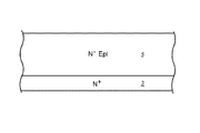
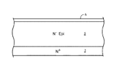
図1に関しては、強くドープされたn+基板3と軽くドープされたn−層5とを含む半導体ウエハの部分図が示されている。この半導体基板はケイ素(Si)からなるのが好ましいが、その他の材料例えば、ガリウムヒ化物(GaAs)、ゲルマニウム(Ge)等から形成してもよい。
図2は、酸化物層6が軽くドープされたn−層5上に成長しているあるいは沈着されているのを示す。図3に関し、第1マスク51(仮想線で図示)が図2の部分的に形成された半導体ディバイスの上側に選択的に当てがわれている。この第1マスク51はフォトレジスト層の沈着あるいは当業者に知られているどれかその他の方法で形成してもよい。発達したフォトレジストは除去され、未発達のフォトレジストが当業界で知られているようにその場所に残る。簡略のため、マスク51とは半導体のある領域がエッチングされ、ドープされ被覆等されるのを防ぐために用いられる材料のことを言う。
溝19はエッチング等の処理で第1マスク51によりカバーされていない領域に形成される。エッチング処理には化学エッチング、プラズマ・エッチング、反応性イオンエッチング(RIE)等でよい。図2の部分的に形成された半導体ディバイスのエッチングにより、複数個のメサ18と複数個の溝19とが、部分的に形成された半導体ディバイスの端子領域に形成される。溝19はエピタキシャル層5から基板(強くドープされた領域)3に向け深さB1により示されている第1深さ位置まで延びているが、必ずしも基板(強くドープされた領域)3までの全ての道のりに亘って延びる必要はない。メサ18に隣接する溝19の各々の幅A1はその他の溝19に対してもほぼ同じである。部分的に形成された半導体ディバイスは端子領域を備えた作動領域を含む。作動領域とは超接合ディバイスが構成される領域である。端子領域とは作動ディバイスが位置しない領域であって、全半導体ウエハあるいはチップ上の作動ディバイスのセル同士を隔離する。よって、作動領域とは半導体ディバイスが形成される領域であって、端子領域は作動ディバイスのセル同士を隔離する領域である。第1の溝形成工程の後、当業界で既知の技術を用いて第1マスク51が取除かれる。
図4は、端子領域に、前にエッチングで形成された溝19(図3)に当業界で周知の方法で酸化物16を充填しているのを示す。任意で、窒化ケイ素(SixNy)のような誘電体の薄層を酸化物16上に沈着させてもよい。十分な冷却期間後、部分的に形成された半導体ディバイスが平坦化される。この平坦化は化学機械研磨(CMP)あるいはいずれかのその他の適切な平坦化技術を用いてなされる。
図5に関し、第2のマスク52(仮想線で図示)が図4の部分的に形成された半導体ディバイス上に選択的に当てがわれる。溝9、17がエッチング等の処理で第2マスクでカバーされていない領域に形成されている。エッチング処理は化学エッチング、プラズマ・エッチング、RIE等でよい。第2のマスクを当てがいエッチング処理により端子領域に残っているエピタキシャル材料を除去し、前回の充填工程で生じた酸化物柱状体8同士の間に溝17を形成し、構造体の作動領域に溝9とメサ11とを形成する。n−層5がエッチングされて、エッチングで形成された溝9、17の底部がn+基板3とn−層5との間のインターフェイス(境界面)に接触あるいは接近している。溝17は第1主表面から基板3に向け、深さB2で示されている第2深さ位置まで延びているが、必ずしも基板3までの全ての道のりに亘って延びる必要はない。酸化物柱状体8に隣接する溝17の各々の幅A2はその他の溝に対してもほぼ同じである。
メサ11は、これを取り巻く端子領域に対向して、作動領域にあるので、「ディバイス・メサ」と言う。このディバイス・メサ11は各トランジスタあるいはこの方法で製造される作動ディバイス・セル用の電圧保持層を形成するために使用される。溝9はエピタキシャル層5の第1主表面から基板3に向け、深さB3で示されている第3深さ位置まで延びているが、必ずしも基板3までの全ての道のりに亘って延びる必要はない。ディバイス・メサ11に隣接する溝9の各々の幅A3はその他の溝9に対してもほぼ同じである。明確には示されていないが、溝の充填工程を容易にするため、溝9の頂部は、その底部に比べて1%から10%広いのが好ましい。よって、メサ11の両側壁面はエピタキシャル層5の第1主表面に対して所定の傾斜を保っている。第2の溝形成処理後、第2のマスク52が当業界で既知の技術を用いて除去される。
半導体基板の表面および/または半導体層および/または溝9、17は必要であれば、以下の工程の1つあるいはそれ以上を用いて平滑にしてもよい。
(i) 溝の表面から(特に、100−1000Å)のシリコン薄層を除去するため等方性プラズマ・エッチングを用いてもよい。
(ii) 棄て二酸化ケイ素層を溝の表面に成長させ、緩衝酸化物エッチングあるいは希釈フッ化水素酸エッチング等のエッチングを用いて除去してもよい。
(i) 溝の表面から(特に、100−1000Å)のシリコン薄層を除去するため等方性プラズマ・エッチングを用いてもよい。
(ii) 棄て二酸化ケイ素層を溝の表面に成長させ、緩衝酸化物エッチングあるいは希釈フッ化水素酸エッチング等のエッチングを用いて除去してもよい。
これらの技術のいずれかあるいは両方を用いることにより残留ストレスおよび望ましくない汚染物を除去しながら丸い角を備えた滑らかな溝表面を作成できる。然し、垂直の両側壁と四角い角を有することが望ましい場合は、異方性エッチングを等方性エッチングの代わりに用いる。異方性エッチングは、一般に、等方性エッチングとは反対に、エッチングをする材料において異なる方向での異なるエッチング率を意味する。
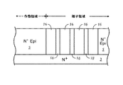
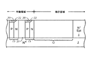
図6に示されているように、図5に示されている第2のマスクの当てがいとエッチング処理とにより、作動領域および端子領域の両領域にそれぞれ形成された溝9、17には酸化物材料が充填され作動領域には酸化物柱状体14がそして端子領域には比較的厚くて広い酸化物領域12(例えば、図11に示す平面図参照)を形成する。酸化物領域12の全体の幅は約20〜60μmである。窒化ケイ素のような絶縁物の薄層10が酸化物上に沈着せられて反りの問題を減少あるいは解消する。
図6の部分的に形成された半導体ディバイスの表面は、次いで、平坦化され、その結果生じる部分的に形成された半導体ディバイスが図7に示されている。図8は、上記と同様の方法により作動領域で溝9に沈着された酸化物14を、マスクを当てがいエッチングをして除去した後生じる部分的に形成された半導体ディバイスである。
図9は、第1所定角度Φ(即ち、第1所定打ち込み角度Φ)から図8の構造体へのイオン打ち込みを示す。第1所定打ち込み角度Φは、溝9の幅A3と深さB3とから決定され(即ち、A3/B3=打ち込み角度Φの正接)、典型的には垂直から約2度から12度である。各溝9の底部にはイオンが打ち込まれないように、イオン打ち込みは角度Φでなされる。周囲への打ち込みの拡散が起きないように、溝9の底部へのイオン打ち込みは避ける。イオン打ち込みは線量範囲1E13から1E14cm−2(即ち、約1×1013から1×1014cm−2)で、エネルギー・レベル、約30−200キロ電子ボルト(KeV)。従って、第1導電形のドーパンとが、隣接する対の複数個の溝にある上記の複数個のディバイス・メサ11と複数個の溝9の所定領域の少なくとも1つのディバイス・メサ11に、1つの溝9の1つの側壁に第1所定打ち込み角度Φで打ち込まれて、その1つの溝9の側壁面に、強くドープされた領域3より低いドープ濃度を有する第1導電形の第1ドープ領域を形成する。この工程から、作動領域のディバイス・メサ11の深さ方向に沿ってp−n結合形成方法が開始する。
図10は、第2所定角度Φ´(即ち、第2所定打ち込み角度Φ´)から図9の構造体へのイオン打ち込みを示す。第2所定打ち込み角度Φ´も、溝9の幅A3と深さB3から決定され(即ち、−(A3/B3)=打ち込み角度Φ´の正接)、典型的には垂直から約−2度から−12度である。各溝9の底部にはイオンが打ち込まれないように、イオン打ち込みは角度Φ´でなされる。第1所定打ち込み角度Φと第2所定打ち込み角度Φ´とはほぼ同じ強度でも異なっていても良い。周囲への打ち込みの拡散が起きないように、溝9の底部へのイオン打ち込みは避ける。イオン打ち込みは線量範囲1E13から1E14cm−2でエネルギー・レベル、約30−200KeVで行なわれる。従って、第2導電形のドーパントが、上記の複数個のディバイス・メサ11と複数個の溝9の所定領域の少なくとも1つのディバイス・メサ11に、第1導電形のドーパントを打ち込んだ側壁とは反対の少なくとも1つのディバイス・メサ11の側壁面に第2所定打ち込み角度Φ´で打ち込まれて、上記の複数個の溝9の少なくとも1つの深さ方向に沿って位置する第1ドープ領域および第2ドープ領域のp−n結合を形成し、イオンを打ち込んでいない作動領域の外側側壁を提供する。このイオン打ち込みで、作動領域のディバイス・メサ11の深さ方向に沿ってのpn結合形成方法が終了する。
ドーピングは、イオン打ち込み、固体拡散、液体拡散、スピン・オン(spin-on)沈着、プラズマ・ドーピング、蒸気相ドーピング、レーザ・ドーピング等の1つにより為される。ホウ素(B)によるドーピングでは、p形領域がより多くでき、リン(P)によるドーピングでは、n形領域がより多くでき、ヒ素(As)によるドーピングでは、n形領域がより多くできる。アンチモン(Sb)、ビスマス(Bi)、アルミニウム(Al)、インジウム(In)、ガリウム(Ga)等のその他のドーパントを基板の材料およびドーピングの所望の強度により用いても良い。ドーピングはイオン打ち込みによるのが好ましい。
イオン打ち込みに続いて、1200℃までの温度で駆動(drive in)工程が12時間までなされ、ディバイス・メサ11がp−n柱状体13に変換される。尚、温度と時間は十分に打ち込まれたドーパントが駆動されるように選択される。然し、上記の、イオン打ち込みを為すのに使用されたエネルギー・レベルはドーパントを十分に駆動するのに足るものであり、本発明から逸脱するものではない。
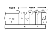
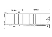
図11はこの方法によって生じた部分的に形成された半導体ディバイスの平面図であり、溝9が作動領域と、端子領域にある広い酸化物領域とにあるn−p柱状体を分離しているのを示す。図11は、部分的に形成された半導体ディバイスの多くの可能な平面図の1つを示す。図11は多角形セル・レイアウトに代え縞模様(即ち、列状のn−p柱状体)を示すが、本実施例は必ずしも多角形セル構造体を排除するものではない。多くの柱状体13と溝9とのその他の幾何学的配置も本発明から逸脱することなく考えられる。柱状体13はn−pに限定されるものではなく、本発明を逸脱することなく、n−p−n、p−n−p、n−pp−n、p−nn−p等でもよい。
どの酸化方法でも溝9を二酸化ケイ素で充填するようにしている(図12)。n−p柱状体13は二酸化ケイ素21で囲まれている。然し、溝9を充填するとディバイスを反らすことが分かった。この反る問題は酸化物上に窒化ケイ素(例えば、SixNy)のような薄い絶縁体層を沈着させることにより軽減あるいは解消できる。図12は、作動領域の溝9が酸化物21で充填され、窒化ケイ素のような薄い絶縁体層192が酸化物21の上に沈着され、部分的に形成された半導体ディバイスの表面が平坦化された後の図10の部分的形成された半導体ディバイスを示す。
図13から図16は上記で生じた構造体上に超接合ディバイスを形成する方法を示す。図13はp+イオンがドープされた領域22が打ち込まれているのを示す。p+イオンでドープされた領域22に形成されたn+イオンでドープされた領域20が図14に示されている。そのn+領域20は超接合ディバイスのソース(源)領域の役割を為す。図15は絶縁ゲート24が沈着され、この絶縁ゲート24にゲート導電体26が沈着されているのを示す。図16はゲート導電体26がもう1つの酸化物層24で被覆されているのを示す。図16は、周知の方法を用いて、図12の部分的に形成された半導体ディバイスに形成された超接合ディバイスを示す。この超接合ディバイスは接触と不動態層を加えることにより今や完成準備状態にある。
不動態化材料は、熱成長、減圧(LP)化学蒸着(CVD)、プラズマ増強化学蒸着(PECVD)、常気圧化学蒸着(APCVD)、スパン・オン・ガラス(SOG)、ガラス・フリット沈着、直接塗布およびこれらの組み合わせのうちの1つを用いて第1あるいは第2主表面に塗布してもよい。不動態化材料は、酸化物、窒化物、ガラス、およびドープされたあるいはドープされないポリシリコンの1つでもよい。
この構造体の上に建造あるいは形成されたディバイスの性能は、従来の半導体トランジスタ・ディバイスに比べて雪崩降伏電圧(Vb)特性を向上した。ついで、従来の金属酸化物半導体電界効果トランジスタ(MOSFET)が作動領域に、周知の工程を用いて形成される。選択的に第2導電形の作動領域を打ち込みし、その後選択的に第1導電形の領域を打ちこんで、追加の工程によりディバイスを完成する。前面および後面への接触もなされ、不動態化層が沈着され、パターン化されてディバイス形成手順が終了する。
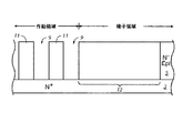
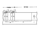
図17から図19に示されている別の実施例では、比較的広い溝30が端子領域に形成されている。この比較的広い溝30の幅はほぼ20−60μmである。図18は、図9及び図10について上記したようにイオン打ち込みが進められているのを示す。ついで、溝30は酸化物で再充填されて図19に示されているように広い酸化物領域12を形成する。この広い酸化物領域12の幅はほぼ20−60μmである。
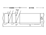
図5に始まる更に別の実施例では、溝9及び17のみが第1主表面に形成されてそれぞれメサ11および8を形成する。端子領域にあるこのメサ8は約1.0から1.5μmの幅を有し、作動領域のメサ11は約4.0から5.0μmの幅を有する。この方法は、更に、作動領域のメサ11の両側壁にドーパントを打ち込む前に複数個の溝9、17およびメサ8、11(図5)の露出面に浅い層の酸化物を形成することを含む。複数個の溝9及び17は、端子領域の約1.0から1.5μmのメサ8の各々が酸化により実質的に消費されるまで酸化される。端子領域に残っている溝17は酸化工程により充填されて作動領域に隣接する端子領域に広い酸化物領域12を作成し、作動領域にある残りの溝9を充填する。この広い酸化物領域12の幅はほぼ20−60μmである。最後に、部分的に形成された半導体ディバイスの表面は平坦化され超接合がその上に形成される。
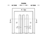
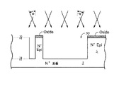
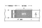
図20−図22に示されている更に別の実施例では、絶縁体上のケイ素(SOI)あるいは単に厚い酸化物ウエハ40が基板3に接着されている。焼きなましあるいは接着工程には焼きなまし炉で数分あるいは数時間基板3とウエハ40とを加熱することを含む。例えば、積層された基板3とウエハ40とは800℃から1200℃の焼きなまし炉に数分から数時間置かれて材料を十分に接着させる。焼きなまし工程は不活性雰囲気、例えば、窒素ガス、酸化雰囲気、例えば、純酸素、酸素・窒素混合物、蒸気等中で行なわれる。湿式焼きなまし中、例えば、蒸気が雰囲気であれば、この蒸気は典型的には800℃より高温で酸素と水素との混合物を用いて発生される。厚い酸化物ウエハ40、例えば、SOIウエハの場合では、その厚い酸化物12の上方のシリコン部分はCMPのような方法により除去される。厚い酸化物ウエハ40の一部分は作動領域を形成するための上記の技術を用いてエッチングにより取除かれる。図21に示されているように、厚いエピタキシャル層5が基板3と残りの酸化物のウエハ40の上に成長している。図22は、部分的に形成された半導体ディバイスが平坦化されて、端子領域には広い酸化物領域12を作動領域にはエピタキシャル層5を残し、これらはエッチングされ、イオンを打ち込まれ、再充填されて、上記のようにn−p柱状体13を形成しているのを示す。
端子領域の比較的広い酸化物領域12を提供することにより、逆電圧防止が作動領域で形成された高電圧ディバイスでは向上されている。
上記より、本発明は、ディバイスの逆電圧阻止能力を向上するため酸化物領域を有する高電圧半導体ディバイスに関することが分かる。本発明の広い発明的概念を逸脱することなく上記の実施例には変更が可能であることは当業者には認識できることである。よって、この発明は開示された特定の実施例に限定されず、その精神の範囲内での変形例もカバーするものと理解される。
Claims (4)
- 作動領域と、この作動領域を取り囲む端子領域とを有する半導体ディバイスの製造方法であって、この方法は、
相互に対向する半導体材料の第1主表面と第2主表面とを備えた半導体基板を提供し、前記半導体基板は、第1導電形の強くドープされた領域を第2主表面に有し、
相互に対向する酸化物材料の第1主表面と第2主表面とを有する酸化物基板を提供し、
前記酸化物基板の前記第2主表面を前記半導体基板の前記第1主表面に接着あるいは焼きなましし、
前記作動領域に近接する前記酸化物基板に溝を形成し、前記溝が前記酸化物基板の前記第1主表面から前記半導体基板の前記第1主表面まで延び、
前記溝をエピタキシャル層で充填することからなるもの。 - 請求項1に記載した方法であって、更に、
第1導電形の柱状体と第2導電形の柱状体を前記作動領域に近接する前記エピタキシャル層に形成することからなり、前記第2導電形のものが前記第1導電形のものと対向しているもの。 - 請求項1に記載した方法であって、更に、
前記エピタキシャル層の前記第1主表面に近接する前記柱状体の少なくとも一部分を第1導電形のドーパントで打ち込むことからなり、前記柱状体の、ドーパントを打ち込んだ部分がゲート領域を形成するもの。 - 請求項1に記載した方法により形成された半導体ディバイス。
Applications Claiming Priority (2)
| Application Number | Priority Date | Filing Date | Title |
|---|---|---|---|
| US63924104P | 2004-12-27 | 2004-12-27 | |
| US60/639,241 | 2004-12-27 |
Related Parent Applications (1)
| Application Number | Title | Priority Date | Filing Date |
|---|---|---|---|
| JP2007548585A Division JP5143567B2 (ja) | 2004-12-27 | 2005-12-27 | 高電圧超接合端子の製造方法 |
Publications (1)
| Publication Number | Publication Date |
|---|---|
| JP2012165012A true JP2012165012A (ja) | 2012-08-30 |
Family
ID=36615484
Family Applications (2)
| Application Number | Title | Priority Date | Filing Date |
|---|---|---|---|
| JP2007548585A Expired - Fee Related JP5143567B2 (ja) | 2004-12-27 | 2005-12-27 | 高電圧超接合端子の製造方法 |
| JP2012100808A Pending JP2012165012A (ja) | 2004-12-27 | 2012-04-26 | 高電圧超接合端子の製造方法 |
Family Applications Before (1)
| Application Number | Title | Priority Date | Filing Date |
|---|---|---|---|
| JP2007548585A Expired - Fee Related JP5143567B2 (ja) | 2004-12-27 | 2005-12-27 | 高電圧超接合端子の製造方法 |
Country Status (7)
| Country | Link |
|---|---|
| US (5) | US7354818B2 (ja) |
| EP (3) | EP2362413B1 (ja) |
| JP (2) | JP5143567B2 (ja) |
| KR (1) | KR20070116219A (ja) |
| CN (1) | CN101421836B (ja) |
| TW (1) | TWI401749B (ja) |
| WO (1) | WO2006071885A2 (ja) |
Cited By (2)
| Publication number | Priority date | Publication date | Assignee | Title |
|---|---|---|---|---|
| CN105702709A (zh) * | 2016-01-29 | 2016-06-22 | 上海华虹宏力半导体制造有限公司 | 沟槽型超级结的制造方法 |
| CN107591451A (zh) * | 2017-08-31 | 2018-01-16 | 上海华虹宏力半导体制造有限公司 | 超结器件 |
Families Citing this family (43)
| Publication number | Priority date | Publication date | Assignee | Title |
|---|---|---|---|---|
| KR100674943B1 (ko) * | 2005-01-15 | 2007-01-26 | 삼성전자주식회사 | Sb,Ga 또는 Bi가 도핑된 반도체 메모리 소자 및 그제조 방법 |
| US7955961B2 (en) * | 2006-03-07 | 2011-06-07 | International Rectifier Corporation | Process for manufacture of trench Schottky |
| US7948033B2 (en) | 2007-02-06 | 2011-05-24 | Semiconductor Components Industries, Llc | Semiconductor device having trench edge termination structure |
| DE102007027626B4 (de) * | 2007-06-12 | 2015-08-06 | Infineon Technologies Austria Ag | Halbleiterbauelement und Verfahren zur Herstellung desselben |
| CN101510557B (zh) | 2008-01-11 | 2013-08-14 | 艾斯莫斯技术有限公司 | 具有电介质终止的超结半导体器件及制造该器件的方法 |
| US7807576B2 (en) * | 2008-06-20 | 2010-10-05 | Fairchild Semiconductor Corporation | Structure and method for forming a thick bottom dielectric (TBD) for trench-gate devices |
| US7943989B2 (en) * | 2008-12-31 | 2011-05-17 | Alpha And Omega Semiconductor Incorporated | Nano-tube MOSFET technology and devices |
| US9508805B2 (en) | 2008-12-31 | 2016-11-29 | Alpha And Omega Semiconductor Incorporated | Termination design for nanotube MOSFET |
| JP5400405B2 (ja) * | 2009-02-05 | 2014-01-29 | 株式会社東芝 | 半導体装置の製造方法 |
| US7910486B2 (en) * | 2009-06-12 | 2011-03-22 | Alpha & Omega Semiconductor, Inc. | Method for forming nanotube semiconductor devices |
| US8299494B2 (en) | 2009-06-12 | 2012-10-30 | Alpha & Omega Semiconductor, Inc. | Nanotube semiconductor devices |
| CN101958283B (zh) * | 2009-07-09 | 2014-07-09 | 上海华虹宏力半导体制造有限公司 | 获得交替排列的p型和n型半导体薄层结构的方法及结构 |
| US20110198689A1 (en) * | 2010-02-17 | 2011-08-18 | Suku Kim | Semiconductor devices containing trench mosfets with superjunctions |
| US8476698B2 (en) * | 2010-02-19 | 2013-07-02 | Alpha And Omega Semiconductor Incorporated | Corner layout for superjunction device |
| CN104538444B (zh) * | 2010-03-05 | 2018-02-23 | 万国半导体股份有限公司 | 带有沟槽‑氧化物‑纳米管超级结的器件结构及制备方法 |
| WO2011158647A1 (ja) * | 2010-06-17 | 2011-12-22 | 富士電機株式会社 | 半導体装置およびその製造方法 |
| US9490372B2 (en) | 2011-01-21 | 2016-11-08 | Semiconductor Components Industries, Llc | Method of forming a semiconductor device termination and structure therefor |
| US8598654B2 (en) | 2011-03-16 | 2013-12-03 | Fairchild Semiconductor Corporation | MOSFET device with thick trench bottom oxide |
| CN104144838B (zh) * | 2011-11-09 | 2017-05-17 | 罗伯特·博世有限公司 | 使用牺牲硅板形成宽沟槽的方法 |
| CN103515450B (zh) * | 2012-06-29 | 2017-02-08 | 朱江 | 一种沟槽电荷补偿肖特基半导体装置及其制造方法 |
| US9112026B2 (en) | 2012-10-17 | 2015-08-18 | Semiconductor Components Industries, Llc | Semiconductor devices and method of making the same |
| CN103022134B (zh) * | 2012-12-06 | 2015-09-09 | 电子科技大学 | 一种超低比导通电阻的soi横向高压功率器件 |
| CN102969358B (zh) * | 2012-12-06 | 2015-08-19 | 电子科技大学 | 一种横向高压功率半导体器件 |
| US8753935B1 (en) | 2012-12-21 | 2014-06-17 | Alpha And Omega Semiconductor Incorporated | High frequency switching MOSFETs with low output capacitance using a depletable P-shield |
| US8951867B2 (en) | 2012-12-21 | 2015-02-10 | Alpha And Omega Semiconductor Incorporated | High density trench-based power MOSFETs with self-aligned active contacts and method for making such devices |
| US8809948B1 (en) | 2012-12-21 | 2014-08-19 | Alpha And Omega Semiconductor Incorporated | Device structure and methods of making high density MOSFETs for load switch and DC-DC applications |
| KR101339265B1 (ko) * | 2012-12-31 | 2013-12-09 | 현대자동차 주식회사 | 반도체 소자의 제조 방법 |
| JP6063280B2 (ja) | 2013-02-05 | 2017-01-18 | ルネサスエレクトロニクス株式会社 | 半導体装置 |
| US9105494B2 (en) | 2013-02-25 | 2015-08-11 | Alpha and Omega Semiconductors, Incorporated | Termination trench for power MOSFET applications |
| US9324784B2 (en) | 2014-04-10 | 2016-04-26 | Semiconductor Components Industries, Llc | Electronic device having a termination region including an insulating region |
| US9343528B2 (en) | 2014-04-10 | 2016-05-17 | Semiconductor Components Industries, Llc | Process of forming an electronic device having a termination region including an insulating region |
| US9508596B2 (en) * | 2014-06-20 | 2016-11-29 | Vishay-Siliconix | Processes used in fabricating a metal-insulator-semiconductor field effect transistor |
| US9171949B1 (en) * | 2014-09-24 | 2015-10-27 | Alpha And Omega Semiconductor Incorporated | Semiconductor device including superjunction structure formed using angled implant process |
| CN104779296B (zh) * | 2015-04-24 | 2018-10-12 | 无锡同方微电子有限公司 | 一种非对称超结mosfet结构及其制作方法 |
| CN104851908A (zh) * | 2015-05-21 | 2015-08-19 | 无锡同方微电子有限公司 | 高压超结mosfet器件终端结构及其制作方法 |
| CN105047718B (zh) * | 2015-08-06 | 2018-07-13 | 无锡紫光微电子有限公司 | 提高耐压能力的mosfet终端结构及方法 |
| CN106783576B (zh) * | 2016-12-20 | 2021-01-26 | 锦州辽晶电子科技有限公司 | 高耐压半导体分立器件芯片二次腐蚀台面工艺 |
| TWI655688B (zh) * | 2018-05-18 | 2019-04-01 | 英屬維爾京群商節能元件控股有限公司 | 具有超接面結構之半導體元件及其製程 |
| CN109119459B (zh) * | 2018-08-14 | 2022-03-08 | 上海华虹宏力半导体制造有限公司 | 沟槽型超级结的制造方法 |
| CN109148562B (zh) * | 2018-08-28 | 2021-08-24 | 上海华虹宏力半导体制造有限公司 | 超级结器件的制造方法 |
| US11764209B2 (en) | 2020-10-19 | 2023-09-19 | MW RF Semiconductors, LLC | Power semiconductor device with forced carrier extraction and method of manufacture |
| CN112289684B (zh) * | 2020-10-28 | 2023-06-30 | 上海华虹宏力半导体制造有限公司 | 功率器件的制作方法及器件 |
| CN112420807B (zh) * | 2020-11-04 | 2021-12-28 | 浙江大学 | 一种超级结器件及其终端 |
Citations (5)
| Publication number | Priority date | Publication date | Assignee | Title |
|---|---|---|---|---|
| JPH11102848A (ja) * | 1997-09-26 | 1999-04-13 | Shin Etsu Handotai Co Ltd | Soiウエーハの製造方法ならびにこの方法で製造されるsoiウエーハ |
| JPH11288858A (ja) * | 1998-01-30 | 1999-10-19 | Canon Inc | Soi基板の再生方法及び再生基板 |
| JP2000331899A (ja) * | 1999-05-21 | 2000-11-30 | Shin Etsu Handotai Co Ltd | Soiウェーハの製造方法およびsoiウェーハ |
| JP2001015591A (ja) * | 1999-06-30 | 2001-01-19 | Toshiba Corp | 半導体装置の製造方法・半導体装置 |
| JP2002164540A (ja) * | 2000-11-27 | 2002-06-07 | Toshiba Corp | 半導体装置 |
Family Cites Families (67)
| Publication number | Priority date | Publication date | Assignee | Title |
|---|---|---|---|---|
| US4158206A (en) | 1977-02-07 | 1979-06-12 | Rca Corporation | Semiconductor device |
| JPS5553462A (en) | 1978-10-13 | 1980-04-18 | Int Rectifier Corp | Mosfet element |
| US4238278A (en) | 1979-06-14 | 1980-12-09 | International Business Machines Corporation | Polycrystalline silicon oxidation method for making shallow and deep isolation trenches |
| US4211582A (en) | 1979-06-28 | 1980-07-08 | International Business Machines Corporation | Process for making large area isolation trenches utilizing a two-step selective etching technique |
| US4491486A (en) | 1981-09-17 | 1985-01-01 | Tokyo Shibaura Denki Kabushiki Kaisha | Method for manufacturing a semiconductor device |
| JPS6276645A (ja) * | 1985-09-30 | 1987-04-08 | Toshiba Corp | 複合半導体結晶体構造 |
| US4895810A (en) | 1986-03-21 | 1990-01-23 | Advanced Power Technology, Inc. | Iopographic pattern delineated power mosfet with profile tailored recessed source |
| US5019522A (en) | 1986-03-21 | 1991-05-28 | Advanced Power Technology, Inc. | Method of making topographic pattern delineated power MOSFET with profile tailored recessed source |
| US5045903A (en) | 1988-05-17 | 1991-09-03 | Advanced Power Technology, Inc. | Topographic pattern delineated power MOSFET with profile tailored recessed source |
| US5472888A (en) | 1988-02-25 | 1995-12-05 | International Rectifier Corporation | Depletion mode power MOSFET with refractory gate and method of making same |
| JPH02193286A (ja) * | 1988-10-19 | 1990-07-30 | Laurel Bank Mach Co Ltd | 硬貨処理機の硬貨除去装置 |
| US4908328A (en) * | 1989-06-06 | 1990-03-13 | National Semiconductor Corporation | High voltage power IC process |
| US4994406A (en) | 1989-11-03 | 1991-02-19 | Motorola Inc. | Method of fabricating semiconductor devices having deep and shallow isolation structures |
| CN1019720B (zh) | 1991-03-19 | 1992-12-30 | 电子科技大学 | 半导体功率器件 |
| US5366914A (en) | 1992-01-29 | 1994-11-22 | Nec Corporation | Vertical power MOSFET structure having reduced cell area |
| JP3037509B2 (ja) | 1992-08-04 | 2000-04-24 | 新日本製鐵株式会社 | 半導体記憶装置の製造方法 |
| US5506421A (en) | 1992-11-24 | 1996-04-09 | Cree Research, Inc. | Power MOSFET in silicon carbide |
| US5308786A (en) * | 1993-09-27 | 1994-05-03 | United Microelectronics Corporation | Trench isolation for both large and small areas by means of silicon nodules after metal etching |
| CN1035294C (zh) | 1993-10-29 | 1997-06-25 | 电子科技大学 | 具有异形掺杂岛的半导体器件耐压层 |
| US5435888A (en) | 1993-12-06 | 1995-07-25 | Sgs-Thomson Microelectronics, Inc. | Enhanced planarization technique for an integrated circuit |
| US5395790A (en) | 1994-05-11 | 1995-03-07 | United Microelectronics Corp. | Stress-free isolation layer |
| US5399507A (en) * | 1994-06-27 | 1995-03-21 | Motorola, Inc. | Fabrication of mixed thin-film and bulk semiconductor substrate for integrated circuit applications |
| KR0151267B1 (ko) * | 1995-05-23 | 1998-12-01 | 문정환 | 반도체장치의 제조방법 |
| EP1408554B1 (de) | 1996-02-05 | 2015-03-25 | Infineon Technologies AG | Durch Feldeffekt steuerbares Halbleiterbauelement |
| US5926713A (en) | 1996-04-17 | 1999-07-20 | Advanced Micro Devices, Inc. | Method for achieving global planarization by forming minimum mesas in large field areas |
| US5744994A (en) | 1996-05-15 | 1998-04-28 | Siliconix Incorporated | Three-terminal power mosfet switch for use as synchronous rectifier or voltage clamp |
| KR0183886B1 (ko) | 1996-06-17 | 1999-04-15 | 김광호 | 반도체장치의 트렌치 소자분리 방법 |
| JP3327135B2 (ja) | 1996-09-09 | 2002-09-24 | 日産自動車株式会社 | 電界効果トランジスタ |
| JP3607016B2 (ja) * | 1996-10-02 | 2005-01-05 | 株式会社半導体エネルギー研究所 | 半導体装置およびその作製方法、並びに携帯型の情報処理端末、ヘッドマウントディスプレイ、ナビゲーションシステム、携帯電話、カメラおよびプロジェクター |
| US5721172A (en) * | 1996-12-02 | 1998-02-24 | Taiwan Semiconductor Manufacturing Company, Ltd. | Self-aligned polish stop layer hard masking method for forming planarized aperture fill layers |
| JP3618517B2 (ja) | 1997-06-18 | 2005-02-09 | 三菱電機株式会社 | 半導体装置およびその製造方法 |
| TW327700B (en) | 1997-07-15 | 1998-03-01 | Mos Electronics Taiwan Inc | The method for using rough oxide mask to form isolating field oxide |
| US5976947A (en) | 1997-08-18 | 1999-11-02 | Micron Technology, Inc. | Method for forming dielectric within a recess |
| US6239463B1 (en) | 1997-08-28 | 2001-05-29 | Siliconix Incorporated | Low resistance power MOSFET or other device containing silicon-germanium layer |
| US6081009A (en) | 1997-11-10 | 2000-06-27 | Intersil Corporation | High voltage mosfet structure |
| DE19801095B4 (de) | 1998-01-14 | 2007-12-13 | Infineon Technologies Ag | Leistungs-MOSFET |
| JP4090518B2 (ja) | 1998-07-23 | 2008-05-28 | 三菱電機株式会社 | 半導体装置およびその製造方法 |
| US6291856B1 (en) | 1998-11-12 | 2001-09-18 | Fuji Electric Co., Ltd. | Semiconductor device with alternating conductivity type layer and method of manufacturing the same |
| DE19854915C2 (de) | 1998-11-27 | 2002-09-05 | Infineon Technologies Ag | MOS-Feldeffekttransistor mit Hilfselektrode |
| US6362510B1 (en) * | 1998-12-07 | 2002-03-26 | Advanced Micro Devices, Inc. | Semiconductor topography having improved active device isolation and reduced dopant migration |
| DE69833743T2 (de) | 1998-12-09 | 2006-11-09 | Stmicroelectronics S.R.L., Agrate Brianza | Herstellungmethode einer integrierte Randstruktur für Hochspannung-Halbleiteranordnungen |
| US6452230B1 (en) | 1998-12-23 | 2002-09-17 | International Rectifier Corporation | High voltage mosgated device with trenches to reduce on-resistance |
| US6190970B1 (en) | 1999-01-04 | 2001-02-20 | Industrial Technology Research Institute | Method of making power MOSFET and IGBT with optimized on-resistance and breakdown voltage |
| US6261923B1 (en) * | 1999-01-04 | 2001-07-17 | Vanguard International Semiconductor Corporation | Method to solve the dishing issue in CMP planarization by using a nitride hard mask for local inverse etchback and CMP |
| US6222229B1 (en) | 1999-02-18 | 2001-04-24 | Cree, Inc. | Self-aligned shield structure for realizing high frequency power MOSFET devices with improved reliability |
| US6198127B1 (en) | 1999-05-19 | 2001-03-06 | Intersil Corporation | MOS-gated power device having extended trench and doping zone and process for forming same |
| EP1058303A1 (en) | 1999-05-31 | 2000-12-06 | STMicroelectronics S.r.l. | Fabrication of VDMOS structure with reduced parasitic effects |
| KR100355034B1 (ko) * | 1999-07-15 | 2002-10-05 | 삼성전자 주식회사 | 선택적 에피택셜 성장층을 가진 반도체 장치 및 그 소자분리방법 |
| DE19964214C2 (de) | 1999-09-07 | 2002-01-17 | Infineon Technologies Ag | Verfahren zur Herstellung einer Driftzone eines Kompensationsbauelements |
| GB9929613D0 (en) | 1999-12-15 | 2000-02-09 | Koninkl Philips Electronics Nv | Manufacture of semiconductor material and devices using that material |
| US6214698B1 (en) | 2000-01-11 | 2001-04-10 | Taiwan Semiconductor Manufacturing Company | Shallow trench isolation methods employing gap filling doped silicon oxide dielectric layer |
| DE10041084A1 (de) * | 2000-08-22 | 2002-03-14 | Infineon Technologies Ag | Verfahren zur Bildung eines dielektrischen Gebiets in einem Halbleitersubstrat |
| US6509220B2 (en) | 2000-11-27 | 2003-01-21 | Power Integrations, Inc. | Method of fabricating a high-voltage transistor |
| US6608350B2 (en) | 2000-12-07 | 2003-08-19 | International Rectifier Corporation | High voltage vertical conduction superjunction semiconductor device |
| US6424007B1 (en) | 2001-01-24 | 2002-07-23 | Power Integrations, Inc. | High-voltage transistor with buried conduction layer |
| US6465325B2 (en) | 2001-02-27 | 2002-10-15 | Fairchild Semiconductor Corporation | Process for depositing and planarizing BPSG for dense trench MOSFET application |
| US20030017622A1 (en) * | 2001-07-20 | 2003-01-23 | Motorola, Inc. | Structure and method for fabricating semiconductor structures with coplanar surfaces |
| CN1331238C (zh) * | 2001-09-19 | 2007-08-08 | 株式会社东芝 | 半导体装置及其制造方法 |
| US6797589B2 (en) | 2001-12-18 | 2004-09-28 | Kionix, Inc. | Insulating micro-structure and method of manufacturing same |
| JPWO2003065459A1 (ja) * | 2002-01-28 | 2005-05-26 | 三菱電機株式会社 | 半導体装置 |
| JP2005127550A (ja) | 2003-10-21 | 2005-05-19 | Twinbird Corp | 携帯型貯蔵庫 |
| KR100994719B1 (ko) * | 2003-11-28 | 2010-11-16 | 페어차일드코리아반도체 주식회사 | 슈퍼정션 반도체장치 |
| EP1706899A4 (en) | 2003-12-19 | 2008-11-26 | Third Dimension 3D Sc Inc | PLANARIZATION PROCESS FOR MANUFACTURING SUPERJUNCTION DEVICE |
| EP1701686A4 (en) * | 2003-12-19 | 2009-07-01 | Third Dimension 3D Sc Inc | METHOD FOR PRODUCING A SUPER-BONDING DEVICE WITH CONVENTIONAL ENDS |
| KR20070038945A (ko) * | 2003-12-19 | 2007-04-11 | 써드 디멘존 세미컨덕터, 인코포레이티드 | 수퍼 접합 장치의 제조 방법 |
| US7023069B2 (en) | 2003-12-19 | 2006-04-04 | Third Dimension (3D) Semiconductor, Inc. | Method for forming thick dielectric regions using etched trenches |
| JP4999464B2 (ja) | 2003-12-19 | 2012-08-15 | サード ディメンジョン (スリーディ) セミコンダクタ インコーポレイテッド | 広いメサを備えた超接合ディバイスの製造方法 |
-
2005
- 2005-12-26 TW TW094146511A patent/TWI401749B/zh not_active IP Right Cessation
- 2005-12-27 JP JP2007548585A patent/JP5143567B2/ja not_active Expired - Fee Related
- 2005-12-27 US US11/318,873 patent/US7354818B2/en not_active Expired - Fee Related
- 2005-12-27 EP EP11004139.9A patent/EP2362413B1/en not_active Not-in-force
- 2005-12-27 EP EP05855642.4A patent/EP1842236B1/en not_active Not-in-force
- 2005-12-27 KR KR1020077017428A patent/KR20070116219A/ko not_active Application Discontinuation
- 2005-12-27 EP EP11004140A patent/EP2362414A1/en not_active Withdrawn
- 2005-12-27 CN CN2005800482592A patent/CN101421836B/zh not_active Expired - Fee Related
- 2005-12-27 WO PCT/US2005/047120 patent/WO2006071885A2/en active Application Filing
-
2008
- 2008-03-21 US US12/053,062 patent/US7759204B2/en not_active Expired - Fee Related
- 2008-03-21 US US12/053,067 patent/US7772086B2/en not_active Expired - Fee Related
- 2008-04-16 US US12/104,131 patent/US20080290442A1/en not_active Abandoned
- 2008-04-16 US US12/104,137 patent/US7622787B2/en not_active Expired - Fee Related
-
2012
- 2012-04-26 JP JP2012100808A patent/JP2012165012A/ja active Pending
Patent Citations (5)
| Publication number | Priority date | Publication date | Assignee | Title |
|---|---|---|---|---|
| JPH11102848A (ja) * | 1997-09-26 | 1999-04-13 | Shin Etsu Handotai Co Ltd | Soiウエーハの製造方法ならびにこの方法で製造されるsoiウエーハ |
| JPH11288858A (ja) * | 1998-01-30 | 1999-10-19 | Canon Inc | Soi基板の再生方法及び再生基板 |
| JP2000331899A (ja) * | 1999-05-21 | 2000-11-30 | Shin Etsu Handotai Co Ltd | Soiウェーハの製造方法およびsoiウェーハ |
| JP2001015591A (ja) * | 1999-06-30 | 2001-01-19 | Toshiba Corp | 半導体装置の製造方法・半導体装置 |
| JP2002164540A (ja) * | 2000-11-27 | 2002-06-07 | Toshiba Corp | 半導体装置 |
Cited By (2)
| Publication number | Priority date | Publication date | Assignee | Title |
|---|---|---|---|---|
| CN105702709A (zh) * | 2016-01-29 | 2016-06-22 | 上海华虹宏力半导体制造有限公司 | 沟槽型超级结的制造方法 |
| CN107591451A (zh) * | 2017-08-31 | 2018-01-16 | 上海华虹宏力半导体制造有限公司 | 超结器件 |
Also Published As
| Publication number | Publication date |
|---|---|
| US20080283956A1 (en) | 2008-11-20 |
| US7759204B2 (en) | 2010-07-20 |
| TW200629429A (en) | 2006-08-16 |
| KR20070116219A (ko) | 2007-12-07 |
| US7622787B2 (en) | 2009-11-24 |
| EP2362414A1 (en) | 2011-08-31 |
| CN101421836A (zh) | 2009-04-29 |
| TWI401749B (zh) | 2013-07-11 |
| US20080164521A1 (en) | 2008-07-10 |
| JP2008535206A (ja) | 2008-08-28 |
| EP1842236A2 (en) | 2007-10-10 |
| EP2362413B1 (en) | 2013-06-26 |
| US20080290442A1 (en) | 2008-11-27 |
| US7772086B2 (en) | 2010-08-10 |
| US20060231915A1 (en) | 2006-10-19 |
| CN101421836B (zh) | 2011-05-11 |
| US20080166855A1 (en) | 2008-07-10 |
| WO2006071885A2 (en) | 2006-07-06 |
| EP1842236A4 (en) | 2010-11-17 |
| JP5143567B2 (ja) | 2013-02-13 |
| WO2006071885A3 (en) | 2008-01-24 |
| US7354818B2 (en) | 2008-04-08 |
| EP2362413A1 (en) | 2011-08-31 |
| EP1842236B1 (en) | 2013-04-17 |
Similar Documents
| Publication | Publication Date | Title |
|---|---|---|
| JP5143567B2 (ja) | 高電圧超接合端子の製造方法 | |
| US7339252B2 (en) | Semiconductor having thick dielectric regions | |
| US7410891B2 (en) | Method of manufacturing a superjunction device | |
| US7052982B2 (en) | Method for manufacturing a superjunction device with wide mesas | |
| US7199006B2 (en) | Planarization method of manufacturing a superjunction device | |
| US9461109B1 (en) | Method of forming superjunction high voltage devices using wafer bonding | |
| US9431286B1 (en) | Deep trench with self-aligned sinker | |
| US8816400B2 (en) | SiGe HBT having deep pseudo buried layer and manufacturing method thereof | |
| JP2002124675A (ja) | 半導体装置およびその製造方法 | |
| KR20070035475A (ko) | 에칭된 트렌치들을 이용하여 두꺼운 유전체 영역들을형성하는 방법 |
Legal Events
| Date | Code | Title | Description |
|---|---|---|---|
| A977 | Report on retrieval |
Free format text: JAPANESE INTERMEDIATE CODE: A971007 Effective date: 20131021 |
|
| A131 | Notification of reasons for refusal |
Free format text: JAPANESE INTERMEDIATE CODE: A131 Effective date: 20131024 |
|
| A02 | Decision of refusal |
Free format text: JAPANESE INTERMEDIATE CODE: A02 Effective date: 20140320 |