JP2010045149A - 不揮発性半導体記憶装置 - Google Patents
不揮発性半導体記憶装置 Download PDFInfo
- Publication number
- JP2010045149A JP2010045149A JP2008207655A JP2008207655A JP2010045149A JP 2010045149 A JP2010045149 A JP 2010045149A JP 2008207655 A JP2008207655 A JP 2008207655A JP 2008207655 A JP2008207655 A JP 2008207655A JP 2010045149 A JP2010045149 A JP 2010045149A
- Authority
- JP
- Japan
- Prior art keywords
- memory
- layer
- columnar
- memory device
- transistor
- Prior art date
- Legal status (The legal status is an assumption and is not a legal conclusion. Google has not performed a legal analysis and makes no representation as to the accuracy of the status listed.)
- Granted
Links
Images


Classifications
-
- H—ELECTRICITY
- H10—SEMICONDUCTOR DEVICES; ELECTRIC SOLID-STATE DEVICES NOT OTHERWISE PROVIDED FOR
- H10B—ELECTRONIC MEMORY DEVICES
- H10B43/00—EEPROM devices comprising charge-trapping gate insulators
- H10B43/20—EEPROM devices comprising charge-trapping gate insulators characterised by three-dimensional arrangements, e.g. with cells on different height levels
-
- G—PHYSICS
- G11—INFORMATION STORAGE
- G11C—STATIC STORES
- G11C16/00—Erasable programmable read-only memories
- G11C16/02—Erasable programmable read-only memories electrically programmable
- G11C16/04—Erasable programmable read-only memories electrically programmable using variable threshold transistors, e.g. FAMOS
- G11C16/0483—Erasable programmable read-only memories electrically programmable using variable threshold transistors, e.g. FAMOS comprising cells having several storage transistors connected in series
-
- G—PHYSICS
- G11—INFORMATION STORAGE
- G11C—STATIC STORES
- G11C5/00—Details of stores covered by group G11C11/00
- G11C5/02—Disposition of storage elements, e.g. in the form of a matrix array
-
- G—PHYSICS
- G11—INFORMATION STORAGE
- G11C—STATIC STORES
- G11C5/00—Details of stores covered by group G11C11/00
- G11C5/02—Disposition of storage elements, e.g. in the form of a matrix array
- G11C5/025—Geometric lay-out considerations of storage- and peripheral-blocks in a semiconductor storage device
-
- G—PHYSICS
- G11—INFORMATION STORAGE
- G11C—STATIC STORES
- G11C5/00—Details of stores covered by group G11C11/00
- G11C5/06—Arrangements for interconnecting storage elements electrically, e.g. by wiring
- G11C5/063—Voltage and signal distribution in integrated semi-conductor memory access lines, e.g. word-line, bit-line, cross-over resistance, propagation delay
-
- G—PHYSICS
- G11—INFORMATION STORAGE
- G11C—STATIC STORES
- G11C8/00—Arrangements for selecting an address in a digital store
- G11C8/14—Word line organisation; Word line lay-out
-
- H—ELECTRICITY
- H10—SEMICONDUCTOR DEVICES; ELECTRIC SOLID-STATE DEVICES NOT OTHERWISE PROVIDED FOR
- H10B—ELECTRONIC MEMORY DEVICES
- H10B43/00—EEPROM devices comprising charge-trapping gate insulators
- H10B43/10—EEPROM devices comprising charge-trapping gate insulators characterised by the top-view layout
-
- H—ELECTRICITY
- H10—SEMICONDUCTOR DEVICES; ELECTRIC SOLID-STATE DEVICES NOT OTHERWISE PROVIDED FOR
- H10B—ELECTRONIC MEMORY DEVICES
- H10B43/00—EEPROM devices comprising charge-trapping gate insulators
- H10B43/20—EEPROM devices comprising charge-trapping gate insulators characterised by three-dimensional arrangements, e.g. with cells on different height levels
- H10B43/23—EEPROM devices comprising charge-trapping gate insulators characterised by three-dimensional arrangements, e.g. with cells on different height levels with source and drain on different levels, e.g. with sloping channels
- H10B43/27—EEPROM devices comprising charge-trapping gate insulators characterised by three-dimensional arrangements, e.g. with cells on different height levels with source and drain on different levels, e.g. with sloping channels the channels comprising vertical portions, e.g. U-shaped channels
-
- H—ELECTRICITY
- H10—SEMICONDUCTOR DEVICES; ELECTRIC SOLID-STATE DEVICES NOT OTHERWISE PROVIDED FOR
- H10D—INORGANIC ELECTRIC SEMICONDUCTOR DEVICES
- H10D30/00—Field-effect transistors [FET]
- H10D30/60—Insulated-gate field-effect transistors [IGFET]
- H10D30/69—IGFETs having charge trapping gate insulators, e.g. MNOS transistors
- H10D30/693—Vertical IGFETs having charge trapping gate insulators
-
- H—ELECTRICITY
- H10—SEMICONDUCTOR DEVICES; ELECTRIC SOLID-STATE DEVICES NOT OTHERWISE PROVIDED FOR
- H10D—INORGANIC ELECTRIC SEMICONDUCTOR DEVICES
- H10D30/00—Field-effect transistors [FET]
- H10D30/60—Insulated-gate field-effect transistors [IGFET]
- H10D30/69—IGFETs having charge trapping gate insulators, e.g. MNOS transistors
- H10D30/694—IGFETs having charge trapping gate insulators, e.g. MNOS transistors characterised by the shapes, relative sizes or dispositions of the gate electrodes
- H10D30/697—IGFETs having charge trapping gate insulators, e.g. MNOS transistors characterised by the shapes, relative sizes or dispositions of the gate electrodes having trapping at multiple separated sites, e.g. multi-particles trapping sites
-
- H—ELECTRICITY
- H10—SEMICONDUCTOR DEVICES; ELECTRIC SOLID-STATE DEVICES NOT OTHERWISE PROVIDED FOR
- H10D—INORGANIC ELECTRIC SEMICONDUCTOR DEVICES
- H10D62/00—Semiconductor bodies, or regions thereof, of devices having potential barriers
- H10D62/10—Shapes, relative sizes or dispositions of the regions of the semiconductor bodies; Shapes of the semiconductor bodies
- H10D62/124—Shapes, relative sizes or dispositions of the regions of semiconductor bodies or of junctions between the regions
- H10D62/125—Shapes of junctions between the regions
Landscapes
- Engineering & Computer Science (AREA)
- Microelectronics & Electronic Packaging (AREA)
- Semiconductor Memories (AREA)
- Non-Volatile Memory (AREA)
Abstract
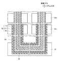
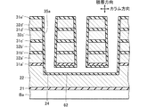
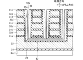
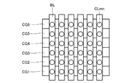
【解決手段】メモリストリングスMSは、基板Baに対して垂直方向に延びる複数の柱状部CLmn、及び複数の柱状部CLmnの下端を連結させるように形成された連結部JPmnを有する半導体層SCmnを有する。ワード線WL1〜4は、この柱状部CLmnを取り囲む板状電極として形成されている。また、選択ゲート線SGは、カラム方向を長手方向として形成され、ビット線BLはロウ方向を長手方向として、1つの柱状部CLmnごとに形成されている。
【選択図】図2
Description
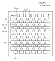
(第1の実施の形態に係る不揮発性半導体記憶装置100の構成)
図1は、本発明の第1の実施の形態に係る不揮発性半導体記憶装置100の概略図を示す。図1に示すように、第1の実施の形態に係る不揮発性半導体記憶装置100は、主として、メモリトランジスタ領域12、ワード線駆動回路13、選択ゲート線駆動回路15、センスアンプ16、及びバックゲートトランジスタ駆動回路18を有する。
次に、図8〜図14を参照して、第1の実施の形態に係る不揮発性半導体記憶装置100の製造方法を説明する。メモリトランジスタ領域12と、図示しない周辺回路領域は同時に形成されるが、ここでは説明の簡単のため、本実施の形態の特徴に関連するメモリトランジスタ領域12の製造工程のみを説明する。
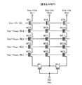
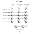
次に、再び図1〜3を参照して、第1の実施の形態に係る不揮発性半導体記憶装置100の動作を説明する。メモリトランジスタMCにおける「書き込み動作」、、「消去動作」、及び「読み出し動作」について説明する。なお、以下では、図3に示すメモリトランジスタMC2を書き込み、読み出しの対象とする場合を例として説明する。
最初に、メモリストリングスMS中の、例えばメモリトランジスタMC2への書き込み動作を、図15を参照して説明する。まず、初期動作として、全てのビット線BL0〜2の電圧を接地電位VSSとし、バックゲート線BGの電圧を接地電位Vssとして、バックゲートトランジスタBT1、BT2を非導通状態に維持しておく。選択ゲートSGの電圧も接地電圧Vssとされ、選択トランジスタST1〜3も非導通状態にされている。
次に、メモリストリングスMS中のメモリトランジスタの消去動作を説明する。
続いて、メモリストリングスMS中の、例えばメモリトランジスタMC2の読み出し動作を、図16を参照して説明する。
次に、第1の実施の形態に係る不揮発性半導体記憶装置100の効果について説明する。第1の実施の形態に係る不揮発性半導体記憶装置100は、上記積層構造に示したように高集積化可能である。また、不揮発性半導体記憶装置100は、上記製造工程にて説明したように、メモリトランジスタMCとなる各層、選択トランジスタ層STとなる各層を、ワード線WLの積層数に関係なく所定のリソグラフィ工程数で製造することができる。すなわち、安価に不揮発性半導体記憶装置100を製造することが可能である。
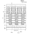
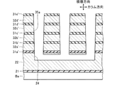
図17は、本発明の第2のの実施の形態に係る不揮発性半導体記憶装置100の、メモリトランジスタ領域12の概略図を示す。図18はその平面図である。なお、第1の実施の形態と同一の構成要素に関しては同一の符号を付し、その説明は省略する。
なお、1つのメモリストリングスMSに含まれる柱状部CLmnの数は3本に限られず、複数であればよい。このとき、1つのメモリストリングスMS中に含まれる柱状部CLmnの数と、メモリトランジスタが形成される柱状部の実効面積との関係は、次のようになる。
柱状部CLmnが3本→6F2
柱状部CLmnが4本→5F2
柱状部CLmnが9本→4.5F2
すなわち、1つのメモリストリングスMS中に含まれる柱状部CLmnの数を増すほど、柱状部CLmnの実効面積を低減でき、メモリの高密度化に寄与することができる。
以上、本発明の実施の形態を説明したが、本発明はこれらに限定されるものではなく、発明の趣旨を逸脱しない範囲内において、様々な変更、追加、削除、置換等が可能である。たとえば、上記の実施の形態では、1つのメモリストリングスを形成する3つの柱状部CLmnを、いずれもポリシリコンを材料として形成すると説明したが、例えば、データが常に消去状態に維持されるメモリトランジスタMC5〜8に沿った柱状部CLmn2については、ポリシリコンの代わりに、例えば表面がコバルト等の金属と反応させてシリサイド化されたシリコン層又は金属膜(アルミニウム等)などの金属元素を含む化合物を用いることも可能である。あるいは、柱状部CLmn2のみ、高濃度の不純物(リン等)を注入して低抵抗化してもよい。この対策により、電圧降下が小さくなり、より安定した読み出し動作を保証できる.
また、上記の実施の形態では、1つのメモリストリングスMS中の少なくとも1列のメモリトランジスタMCは、常に消去状態に維持されるのが好ましいと説明したが、これに限らず、このような常に消去状態に維持されるメモリトランジスタMCを設けないこととしてもよい。この場合、選択ワード線WLの電位を接地電位Vssよりも高く設定する必要があり、読み出し電流量が最悪の場合第1の実施の形態の場合の半分程度に減少する可能性があるが、十分な感度のセンスアンプとノイズ対策が施されれば読み出し可能である。この場合、より有効なセルアレイ利用が可能となり、1つのメモリストリングスMSに含まれる柱状部の数に関わらず、4F2の柱状部の面積を実現でき、半導体メモリ装置の高密度化に寄与するものである。
Claims (5)
- 電気的に書き換え可能な複数のメモリセルと選択トランジスタとが直列に接続された複数のメモリストリングスを有する不揮発性半導体記憶装置であって、
前記メモリストリングスは、
基板に対して垂直方向に延びる複数の柱状部、及び前記複数の柱状部の下端を連結させるように第1方向を長手方向として形成された連結部を有する半導体層と、
前記柱状部の側面を取り囲むように形成された電荷蓄積層と、
前記柱状部の側面及び前記電荷蓄積層を取り囲むように複数層を積層して形成され前記メモリセルの制御電極として機能する複数の第1導電層と、
前記第1方向に並ぶ前記複数の柱状部の周りにゲート絶縁膜を介して前記第1方向を長手方向として形成され前記選択トランジスタの制御電極として機能する第2導電層と、
前記複数の柱状部のそれぞれに接続され前記第1方向と直交する第2方向を長手方向として形成されるビット線と
を備えたことを特徴とする不揮発性半導体記憶装置。 - 前記連結部に絶縁膜を介して接するように形成され前記連結部に形成されるバックゲートトランジスタの制御電極として機能するバックゲート層を更に備えたことを特徴とする請求項1に記載の不揮発性半導体記憶装置。
- 前記第1導電層は、前記基板上に2次元的に配列された複数の前記メモリストリングスに共通に接続される板状電極であることを特徴とする請求項1記載の不揮発性半導体記憶装置。
- 1つの前記メモリストリングスを構成する前記複数の柱状部のうち、少なくとも1つの柱状部に沿って形成される前記メモリセルは、常に消去状態に維持されることを特徴とする請求項1記載の不揮発性半導体記憶装置。
- 1つの前記メモリストリングスを構成する前記複数の柱状部の少なくとも1つは金属元素を含む化合物であることを特徴とする請求項1記載の不揮発性半導体記憶装置。
Priority Applications (4)
| Application Number | Priority Date | Filing Date | Title |
|---|---|---|---|
| JP2008207655A JP5288936B2 (ja) | 2008-08-12 | 2008-08-12 | 不揮発性半導体記憶装置 |
| US12/501,142 US8008710B2 (en) | 2008-08-12 | 2009-07-10 | Non-volatile semiconductor storage device |
| TW098124154A TWI400792B (zh) | 2008-08-12 | 2009-07-16 | 非揮發性半導體儲存裝置 |
| KR1020090073728A KR101031699B1 (ko) | 2008-08-12 | 2009-08-11 | 비휘발성 반도체 저장 장치 |
Applications Claiming Priority (1)
| Application Number | Priority Date | Filing Date | Title |
|---|---|---|---|
| JP2008207655A JP5288936B2 (ja) | 2008-08-12 | 2008-08-12 | 不揮発性半導体記憶装置 |
Publications (2)
| Publication Number | Publication Date |
|---|---|
| JP2010045149A true JP2010045149A (ja) | 2010-02-25 |
| JP5288936B2 JP5288936B2 (ja) | 2013-09-11 |
Family
ID=41680700
Family Applications (1)
| Application Number | Title | Priority Date | Filing Date |
|---|---|---|---|
| JP2008207655A Expired - Fee Related JP5288936B2 (ja) | 2008-08-12 | 2008-08-12 | 不揮発性半導体記憶装置 |
Country Status (4)
| Country | Link |
|---|---|
| US (1) | US8008710B2 (ja) |
| JP (1) | JP5288936B2 (ja) |
| KR (1) | KR101031699B1 (ja) |
| TW (1) | TWI400792B (ja) |
Cited By (8)
| Publication number | Priority date | Publication date | Assignee | Title |
|---|---|---|---|---|
| JP2011198806A (ja) * | 2010-03-17 | 2011-10-06 | Toshiba Corp | 半導体記憶装置及びその製造方法 |
| KR101113766B1 (ko) * | 2010-12-31 | 2012-02-29 | 주식회사 하이닉스반도체 | 비휘발성메모리장치 및 그 제조 방법 |
| JP2012204430A (ja) * | 2011-03-24 | 2012-10-22 | Toshiba Corp | 不揮発性半導体記憶装置及びその製造方法 |
| US8349689B2 (en) | 2010-05-31 | 2013-01-08 | Hynix Semiconductor Inc. | Non-volatile memory device and method for fabricating the same |
| US8455941B2 (en) | 2010-06-22 | 2013-06-04 | Kabushiki Kaisha Toshiba | Nonvolatile semiconductor memory device and method for manufacturing the same |
| US8817538B2 (en) | 2011-06-14 | 2014-08-26 | Kabushiki Kaisha Toshiba | Nonvolatile semiconductor memory device and method for erasing data thereof |
| US8902670B2 (en) | 2012-08-31 | 2014-12-02 | Kabushiki Kaisha Toshiba | Semiconductor memory device |
| JP2015525971A (ja) * | 2012-07-06 | 2015-09-07 | マイクロン テクノロジー, インク. | 少なくとも2個のマスクを使用する階段形成 |
Families Citing this family (210)
| Publication number | Priority date | Publication date | Assignee | Title |
|---|---|---|---|---|
| JP5016832B2 (ja) * | 2006-03-27 | 2012-09-05 | 株式会社東芝 | 不揮発性半導体記憶装置及びその製造方法 |
| JP5142692B2 (ja) | 2007-12-11 | 2013-02-13 | 株式会社東芝 | 不揮発性半導体記憶装置 |
| KR101539699B1 (ko) | 2009-03-19 | 2015-07-27 | 삼성전자주식회사 | 3차원 구조의 비휘발성 메모리 소자 및 그 제조방법 |
| KR101543331B1 (ko) * | 2009-07-06 | 2015-08-10 | 삼성전자주식회사 | 메탈 소스 라인을 갖는 수직 구조의 비휘발성 메모리 소자의 제조방법 |
| JP2011040706A (ja) * | 2009-07-15 | 2011-02-24 | Toshiba Corp | 不揮発性半導体記憶装置 |
| JP5380190B2 (ja) * | 2009-07-21 | 2014-01-08 | 株式会社東芝 | 不揮発性半導体記憶装置及びその製造方法 |
| KR101164954B1 (ko) | 2009-09-14 | 2012-07-12 | 에스케이하이닉스 주식회사 | 3차원 구조를 갖는 비휘발성 메모리 소자 및 그 제조 방법 |
| JP2011061159A (ja) * | 2009-09-14 | 2011-03-24 | Toshiba Corp | 不揮発性半導体記憶装置 |
| KR20110042619A (ko) * | 2009-10-19 | 2011-04-27 | 삼성전자주식회사 | 3차원 반도체 장치 및 그 제조 방법 |
| KR101559958B1 (ko) * | 2009-12-18 | 2015-10-13 | 삼성전자주식회사 | 3차원 반도체 장치의 제조 방법 및 이에 따라 제조된 3차원 반도체 장치 |
| KR101658479B1 (ko) | 2010-02-09 | 2016-09-21 | 삼성전자주식회사 | 불휘발성 메모리 장치, 그것의 동작 방법, 그리고 그것을 포함하는 메모리 시스템 |
| US9378831B2 (en) | 2010-02-09 | 2016-06-28 | Samsung Electronics Co., Ltd. | Nonvolatile memory devices, operating methods thereof and memory systems including the same |
| US9324440B2 (en) | 2010-02-09 | 2016-04-26 | Samsung Electronics Co., Ltd. | Nonvolatile memory devices, operating methods thereof and memory systems including the same |
| KR101691088B1 (ko) | 2010-02-17 | 2016-12-29 | 삼성전자주식회사 | 불휘발성 메모리 장치, 그것의 동작 방법, 그리고 그것을 포함하는 메모리 시스템 |
| KR101691092B1 (ko) | 2010-08-26 | 2016-12-30 | 삼성전자주식회사 | 불휘발성 메모리 장치, 그것의 동작 방법, 그리고 그것을 포함하는 메모리 시스템 |
| JP5788183B2 (ja) | 2010-02-17 | 2015-09-30 | 三星電子株式会社Samsung Electronics Co.,Ltd. | 不揮発性メモリ装置、それの動作方法、そしてそれを含むメモリシステム |
| US8923060B2 (en) | 2010-02-17 | 2014-12-30 | Samsung Electronics Co., Ltd. | Nonvolatile memory devices and operating methods thereof |
| US8908431B2 (en) | 2010-02-17 | 2014-12-09 | Samsung Electronics Co., Ltd. | Control method of nonvolatile memory device |
| JP2011170956A (ja) | 2010-02-18 | 2011-09-01 | Samsung Electronics Co Ltd | 不揮発性メモリ装置およびそのプログラム方法と、それを含むメモリシステム |
| US8792282B2 (en) | 2010-03-04 | 2014-07-29 | Samsung Electronics Co., Ltd. | Nonvolatile memory devices, memory systems and computing systems |
| US8553466B2 (en) | 2010-03-04 | 2013-10-08 | Samsung Electronics Co., Ltd. | Non-volatile memory device, erasing method thereof, and memory system including the same |
| KR101083637B1 (ko) | 2010-05-31 | 2011-11-16 | 주식회사 하이닉스반도체 | 비휘발성 메모리 장치 및 그 제조 방법 |
| KR101818793B1 (ko) * | 2010-06-30 | 2018-02-21 | 샌디스크 테크놀로지스 엘엘씨 | 초고밀도 수직 nand 메모리 장치 및 이를 제조하는 방법 |
| US8349681B2 (en) | 2010-06-30 | 2013-01-08 | Sandisk Technologies Inc. | Ultrahigh density monolithic, three dimensional vertical NAND memory device |
| US9159739B2 (en) | 2010-06-30 | 2015-10-13 | Sandisk Technologies Inc. | Floating gate ultrahigh density vertical NAND flash memory |
| US8187936B2 (en) | 2010-06-30 | 2012-05-29 | SanDisk Technologies, Inc. | Ultrahigh density vertical NAND memory device and method of making thereof |
| US8928061B2 (en) | 2010-06-30 | 2015-01-06 | SanDisk Technologies, Inc. | Three dimensional NAND device with silicide containing floating gates |
| US8193054B2 (en) | 2010-06-30 | 2012-06-05 | SanDisk Technologies, Inc. | Ultrahigh density vertical NAND memory device and method of making thereof |
| US9397093B2 (en) | 2013-02-08 | 2016-07-19 | Sandisk Technologies Inc. | Three dimensional NAND device with semiconductor, metal or silicide floating gates and method of making thereof |
| US10128261B2 (en) | 2010-06-30 | 2018-11-13 | Sandisk Technologies Llc | Cobalt-containing conductive layers for control gate electrodes in a memory structure |
| US8198672B2 (en) | 2010-06-30 | 2012-06-12 | SanDisk Technologies, Inc. | Ultrahigh density vertical NAND memory device |
| KR101688604B1 (ko) * | 2010-07-05 | 2016-12-23 | 삼성전자주식회사 | 3차원 반도체 장치 및 그 제조 방법 |
| JP2013012553A (ja) | 2011-06-28 | 2013-01-17 | Toshiba Corp | 半導体記憶装置 |
| JP5543950B2 (ja) * | 2011-09-22 | 2014-07-09 | 株式会社東芝 | 不揮発性半導体記憶装置の製造方法及び不揮発性半導体記憶装置 |
| KR20130070153A (ko) * | 2011-12-19 | 2013-06-27 | 에스케이하이닉스 주식회사 | 반도체 장치의 캐패시터, 레지스터, 메모리 시스템 및 이들의 제조 방법 |
| US8878278B2 (en) | 2012-03-21 | 2014-11-04 | Sandisk Technologies Inc. | Compact three dimensional vertical NAND and method of making thereof |
| US8847302B2 (en) | 2012-04-10 | 2014-09-30 | Sandisk Technologies Inc. | Vertical NAND device with low capacitance and silicided word lines |
| KR101957897B1 (ko) * | 2012-04-26 | 2019-03-13 | 에스케이하이닉스 주식회사 | 가변 저항 메모리 장치 및 그 제조 방법 |
| US8828884B2 (en) | 2012-05-23 | 2014-09-09 | Sandisk Technologies Inc. | Multi-level contact to a 3D memory array and method of making |
| KR20130136249A (ko) | 2012-06-04 | 2013-12-12 | 에스케이하이닉스 주식회사 | 반도체 장치 및 그 제조 방법 |
| USRE49831E1 (en) | 2012-06-04 | 2024-02-06 | SK Hynix Inc. | 3D semiconductor memory device |
| US10367001B2 (en) | 2012-06-04 | 2019-07-30 | SK Hynix Inc. | 3D semiconductor memory device |
| US8658499B2 (en) | 2012-07-09 | 2014-02-25 | Sandisk Technologies Inc. | Three dimensional NAND device and method of charge trap layer separation and floating gate formation in the NAND device |
| KR102003526B1 (ko) | 2012-07-31 | 2019-07-25 | 삼성전자주식회사 | 반도체 메모리 소자 및 그 제조방법 |
| US8614126B1 (en) | 2012-08-15 | 2013-12-24 | Sandisk Technologies Inc. | Method of making a three-dimensional memory array with etch stop |
| KR102002802B1 (ko) | 2012-09-05 | 2019-07-23 | 삼성전자주식회사 | 반도체 장치 |
| KR102031187B1 (ko) | 2012-10-05 | 2019-10-14 | 삼성전자주식회사 | 수직형 메모리 장치 |
| US9287167B2 (en) | 2012-10-05 | 2016-03-15 | Samsung Electronics Co., Ltd. | Vertical type memory device |
| US9129861B2 (en) | 2012-10-05 | 2015-09-08 | Samsung Electronics Co., Ltd. | Memory device |
| KR20140062636A (ko) | 2012-11-14 | 2014-05-26 | 에스케이하이닉스 주식회사 | 반도체 장치 및 그 제조 방법 |
| US9230987B2 (en) | 2014-02-20 | 2016-01-05 | Sandisk Technologies Inc. | Multilevel memory stack structure and methods of manufacturing the same |
| US9698153B2 (en) | 2013-03-12 | 2017-07-04 | Sandisk Technologies Llc | Vertical NAND and method of making thereof using sequential stack etching and self-aligned landing pad |
| US8946023B2 (en) | 2013-03-12 | 2015-02-03 | Sandisk Technologies Inc. | Method of making a vertical NAND device using sequential etching of multilayer stacks |
| US9515080B2 (en) | 2013-03-12 | 2016-12-06 | Sandisk Technologies Llc | Vertical NAND and method of making thereof using sequential stack etching and landing pad |
| US9449982B2 (en) | 2013-03-12 | 2016-09-20 | Sandisk Technologies Llc | Method of making a vertical NAND device using a sacrificial layer with air gap and sequential etching of multilayer stacks |
| JP2014187191A (ja) * | 2013-03-22 | 2014-10-02 | Toshiba Corp | 半導体記憶装置の製造方法及び半導体記憶装置 |
| US9093480B2 (en) | 2013-04-01 | 2015-07-28 | Sandisk Technologies Inc. | Spacer passivation for high aspect ratio etching of multilayer stacks for three dimensional NAND device |
| US9099496B2 (en) | 2013-04-01 | 2015-08-04 | Sandisk Technologies Inc. | Method of forming an active area with floating gate negative offset profile in FG NAND memory |
| US9437606B2 (en) | 2013-07-02 | 2016-09-06 | Sandisk Technologies Llc | Method of making a three-dimensional memory array with etch stop |
| US9252151B2 (en) | 2013-07-08 | 2016-02-02 | Sandisk Technologies Inc. | Three dimensional NAND device with birds beak containing floating gates and method of making thereof |
| JP2015028990A (ja) | 2013-07-30 | 2015-02-12 | 株式会社東芝 | 不揮発性記憶装置 |
| US9230980B2 (en) | 2013-09-15 | 2016-01-05 | Sandisk Technologies Inc. | Single-semiconductor-layer channel in a memory opening for a three-dimensional non-volatile memory device |
| KR102242022B1 (ko) | 2013-09-16 | 2021-04-21 | 삼성전자주식회사 | 불휘발성 메모리 및 그것의 프로그램 방법 |
| US9460931B2 (en) | 2013-09-17 | 2016-10-04 | Sandisk Technologies Llc | High aspect ratio memory hole channel contact formation |
| US9496274B2 (en) | 2013-09-17 | 2016-11-15 | Sandisk Technologies Llc | Three-dimensional non-volatile memory device |
| KR20150050878A (ko) | 2013-11-01 | 2015-05-11 | 에스케이하이닉스 주식회사 | 메모리 스트링 및 이를 포함하는 반도체 장치 |
| KR102161814B1 (ko) | 2013-11-19 | 2020-10-06 | 삼성전자주식회사 | 수직형 메모리 장치 및 그 제조 방법 |
| US9449983B2 (en) | 2013-12-19 | 2016-09-20 | Sandisk Technologies Llc | Three dimensional NAND device with channel located on three sides of lower select gate and method of making thereof |
| CN104766863B (zh) * | 2014-01-06 | 2017-09-15 | 旺宏电子股份有限公司 | 三维存储器及其制造方法 |
| US9230905B2 (en) | 2014-01-08 | 2016-01-05 | Sandisk 3D Llc | Trench multilevel contact to a 3D memory array and method of making thereof |
| US9343507B2 (en) | 2014-03-12 | 2016-05-17 | Sandisk 3D Llc | Dual channel vertical field effect transistor including an embedded electrode |
| US9331088B2 (en) | 2014-03-25 | 2016-05-03 | Sandisk 3D Llc | Transistor device with gate bottom isolation and method of making thereof |
| US9224747B2 (en) | 2014-03-26 | 2015-12-29 | Sandisk Technologies Inc. | Vertical NAND device with shared word line steps |
| US9331094B2 (en) | 2014-04-30 | 2016-05-03 | Sandisk Technologies Inc. | Method of selective filling of memory openings |
| US9552991B2 (en) | 2014-04-30 | 2017-01-24 | Sandisk Technologies Llc | Trench vertical NAND and method of making thereof |
| US9244865B2 (en) * | 2014-05-28 | 2016-01-26 | SanDisk Technologies, Inc. | Obtaining diagnostic information through host interfaces |
| US9548313B2 (en) * | 2014-05-30 | 2017-01-17 | Sandisk Technologies Llc | Method of making a monolithic three dimensional NAND string using a select gate etch stop layer |
| US9553146B2 (en) | 2014-06-05 | 2017-01-24 | Sandisk Technologies Llc | Three dimensional NAND device having a wavy charge storage layer |
| US9524779B2 (en) | 2014-06-24 | 2016-12-20 | Sandisk Technologies Llc | Three dimensional vertical NAND device with floating gates |
| US9768270B2 (en) | 2014-06-25 | 2017-09-19 | Sandisk Technologies Llc | Method of selectively depositing floating gate material in a memory device |
| US9379124B2 (en) | 2014-06-25 | 2016-06-28 | Sandisk Technologies Inc. | Vertical floating gate NAND with selectively deposited ALD metal films |
| US9455263B2 (en) | 2014-06-27 | 2016-09-27 | Sandisk Technologies Llc | Three dimensional NAND device with channel contacting conductive source line and method of making thereof |
| US9397107B2 (en) | 2014-06-30 | 2016-07-19 | Sandisk Technologies Llc | Methods of making three dimensional NAND devices |
| US9305932B2 (en) | 2014-06-30 | 2016-04-05 | Sandisk Technologies Inc. | Methods of making three dimensional NAND devices |
| US9177966B1 (en) | 2014-07-08 | 2015-11-03 | Sandisk Technologies Inc. | Three dimensional NAND devices with air gap or low-k core |
| US9570460B2 (en) | 2014-07-29 | 2017-02-14 | Sandisk Technologies Llc | Spacer passivation for high-aspect ratio opening film removal and cleaning |
| US9356031B2 (en) | 2014-08-11 | 2016-05-31 | Sandisk Technologies Inc. | Three dimensional NAND string memory devices with voids enclosed between control gate electrodes |
| US9136130B1 (en) | 2014-08-11 | 2015-09-15 | Sandisk Technologies Inc. | Three dimensional NAND string with discrete charge trap segments |
| US9583539B2 (en) | 2014-08-19 | 2017-02-28 | Sandisk Technologies Llc | Word line connection for memory device and method of making thereof |
| US9230983B1 (en) | 2014-08-20 | 2016-01-05 | Sandisk Technologies Inc. | Metal word lines for three dimensional memory devices |
| US9601502B2 (en) | 2014-08-26 | 2017-03-21 | Sandisk Technologies Llc | Multiheight contact via structures for a multilevel interconnect structure |
| US9576975B2 (en) | 2014-08-26 | 2017-02-21 | Sandisk Technologies Llc | Monolithic three-dimensional NAND strings and methods of fabrication thereof |
| US9236392B1 (en) | 2014-08-26 | 2016-01-12 | Sandisk Technologies Inc. | Multiheight electrically conductive via contacts for a multilevel interconnect structure |
| US9401309B2 (en) | 2014-08-26 | 2016-07-26 | Sandisk Technologies Llc | Multiheight contact via structures for a multilevel interconnect structure |
| US9230974B1 (en) | 2014-08-26 | 2016-01-05 | Sandisk Technologies Inc. | Methods of selective removal of blocking dielectric in NAND memory strings |
| US9362298B2 (en) | 2014-09-11 | 2016-06-07 | Kabushiki Kaisha Toshiba | Non-volatile semiconductor memory device and manufacturing method thereof |
| US9431419B2 (en) | 2014-09-12 | 2016-08-30 | Kabushiki Kaisha Toshiba | Semiconductor memory device and method for manufacturing same |
| US9666590B2 (en) | 2014-09-24 | 2017-05-30 | Sandisk Technologies Llc | High stack 3D memory and method of making |
| US9515085B2 (en) | 2014-09-26 | 2016-12-06 | Sandisk Technologies Llc | Vertical memory device with bit line air gap |
| US9305934B1 (en) | 2014-10-17 | 2016-04-05 | Sandisk Technologies Inc. | Vertical NAND device containing peripheral devices on epitaxial semiconductor pedestal |
| US9230979B1 (en) | 2014-10-31 | 2016-01-05 | Sandisk Technologies Inc. | High dielectric constant etch stop layer for a memory structure |
| US9305849B1 (en) | 2014-11-12 | 2016-04-05 | Sandisk Technologies Inc. | Method of making a three dimensional NAND device |
| US9236396B1 (en) | 2014-11-12 | 2016-01-12 | Sandisk Technologies Inc. | Three dimensional NAND device and method of making thereof |
| US9698152B2 (en) | 2014-11-13 | 2017-07-04 | Sandisk Technologies Llc | Three-dimensional memory structure with multi-component contact via structure and method of making thereof |
| US9698223B2 (en) | 2014-11-25 | 2017-07-04 | Sandisk Technologies Llc | Memory device containing stress-tunable control gate electrodes |
| US9570455B2 (en) | 2014-11-25 | 2017-02-14 | Sandisk Technologies Llc | Metal word lines for three dimensional memory devices |
| US9496419B2 (en) | 2014-11-25 | 2016-11-15 | Sandisk Technologies Llc | Ruthenium nucleation layer for control gate electrodes in a memory structure |
| US9793288B2 (en) | 2014-12-04 | 2017-10-17 | Sandisk Technologies Llc | Methods of fabricating memory device with spaced-apart semiconductor charge storage regions |
| US9754956B2 (en) | 2014-12-04 | 2017-09-05 | Sandisk Technologies Llc | Uniform thickness blocking dielectric portions in a three-dimensional memory structure |
| US9553100B2 (en) | 2014-12-04 | 2017-01-24 | Sandisk Techologies Llc | Selective floating gate semiconductor material deposition in a three-dimensional memory structure |
| US10741572B2 (en) | 2015-02-04 | 2020-08-11 | Sandisk Technologies Llc | Three-dimensional memory device having multilayer word lines containing selectively grown cobalt or ruthenium and method of making the same |
| US9984963B2 (en) | 2015-02-04 | 2018-05-29 | Sandisk Technologies Llc | Cobalt-containing conductive layers for control gate electrodes in a memory structure |
| US9780182B2 (en) | 2015-02-04 | 2017-10-03 | Sandisk Technologies Llc | Molybdenum-containing conductive layers for control gate electrodes in a memory structure |
| US9356034B1 (en) | 2015-02-05 | 2016-05-31 | Sandisk Technologies Inc. | Multilevel interconnect structure and methods of manufacturing the same |
| US9419058B1 (en) | 2015-02-05 | 2016-08-16 | Sandisk Technologies Llc | Memory device with comb-shaped electrode having a plurality of electrode fingers and method of making thereof |
| US9484296B2 (en) | 2015-02-12 | 2016-11-01 | Sandisk Technologies Llc | Self-aligned integrated line and via structure for a three-dimensional semiconductor device |
| US9583615B2 (en) | 2015-02-17 | 2017-02-28 | Sandisk Technologies Llc | Vertical transistor and local interconnect structure |
| US9698202B2 (en) | 2015-03-02 | 2017-07-04 | Sandisk Technologies Llc | Parallel bit line three-dimensional resistive random access memory |
| US9870945B2 (en) | 2015-03-10 | 2018-01-16 | Sandisk Technologies Llc | Crystalline layer stack for forming conductive layers in a three-dimensional memory structure |
| US9530788B2 (en) | 2015-03-17 | 2016-12-27 | Sandisk Technologies Llc | Metallic etch stop layer in a three-dimensional memory structure |
| CN106158846B (zh) * | 2015-03-31 | 2019-08-20 | 旺宏电子股份有限公司 | 存储元件及其制造方法 |
| US9799671B2 (en) | 2015-04-07 | 2017-10-24 | Sandisk Technologies Llc | Three-dimensional integration schemes for reducing fluorine-induced electrical shorts |
| US9601508B2 (en) | 2015-04-27 | 2017-03-21 | Sandisk Technologies Llc | Blocking oxide in memory opening integration scheme for three-dimensional memory structure |
| US9397046B1 (en) | 2015-04-29 | 2016-07-19 | Sandisk Technologies Llc | Fluorine-free word lines for three-dimensional memory devices |
| US9627403B2 (en) | 2015-04-30 | 2017-04-18 | Sandisk Technologies Llc | Multilevel memory stack structure employing support pillar structures |
| US10074661B2 (en) | 2015-05-08 | 2018-09-11 | Sandisk Technologies Llc | Three-dimensional junction memory device and method reading thereof using hole current detection |
| US9666281B2 (en) | 2015-05-08 | 2017-05-30 | Sandisk Technologies Llc | Three-dimensional P-I-N memory device and method reading thereof using hole current detection |
| JP2016225614A (ja) * | 2015-05-26 | 2016-12-28 | 株式会社半導体エネルギー研究所 | 半導体装置 |
| KR20160138765A (ko) * | 2015-05-26 | 2016-12-06 | 에스케이하이닉스 주식회사 | 슬리밍 구조물을 포함하는 반도체 메모리 장치 |
| US9859422B2 (en) | 2015-05-28 | 2018-01-02 | Sandisk Technologies Llc | Field effect transistor with elevated active regions and methods of manufacturing the same |
| US9443861B1 (en) | 2015-05-28 | 2016-09-13 | Sandisk Technologies Llc | Fluorine-blocking insulating spacer for backside contact structure of three-dimensional memory structures |
| US9646981B2 (en) | 2015-06-15 | 2017-05-09 | Sandisk Technologies Llc | Passive devices for integration with three-dimensional memory devices |
| US9589981B2 (en) | 2015-06-15 | 2017-03-07 | Sandisk Technologies Llc | Passive devices for integration with three-dimensional memory devices |
| US9419012B1 (en) | 2015-06-19 | 2016-08-16 | Sandisk Technologies Llc | Three-dimensional memory structure employing air gap isolation |
| US9356043B1 (en) | 2015-06-22 | 2016-05-31 | Sandisk Technologies Inc. | Three-dimensional memory devices containing memory stack structures with position-independent threshold voltage |
| US10622368B2 (en) | 2015-06-24 | 2020-04-14 | Sandisk Technologies Llc | Three-dimensional memory device with semicircular metal-semiconductor alloy floating gate electrodes and methods of making thereof |
| US9613977B2 (en) | 2015-06-24 | 2017-04-04 | Sandisk Technologies Llc | Differential etch of metal oxide blocking dielectric layer for three-dimensional memory devices |
| US9530785B1 (en) | 2015-07-21 | 2016-12-27 | Sandisk Technologies Llc | Three-dimensional memory devices having a single layer channel and methods of making thereof |
| US9627399B2 (en) | 2015-07-24 | 2017-04-18 | Sandisk Technologies Llc | Three-dimensional memory device with metal and silicide control gates |
| US9449987B1 (en) | 2015-08-21 | 2016-09-20 | Sandisk Technologies Llc | Three dimensional memory device with epitaxial semiconductor pedestal for peripheral transistors |
| US9543318B1 (en) | 2015-08-21 | 2017-01-10 | Sandisk Technologies Llc | Three dimensional memory device with epitaxial semiconductor pedestal for peripheral transistors |
| US9502471B1 (en) | 2015-08-25 | 2016-11-22 | Sandisk Technologies Llc | Multi tier three-dimensional memory devices including vertically shared bit lines |
| US9853043B2 (en) | 2015-08-25 | 2017-12-26 | Sandisk Technologies Llc | Method of making a multilevel memory stack structure using a cavity containing a sacrificial fill material |
| KR20170027571A (ko) * | 2015-09-02 | 2017-03-10 | 에스케이하이닉스 주식회사 | 반도체 장치 및 그 제조방법 |
| US9806089B2 (en) | 2015-09-21 | 2017-10-31 | Sandisk Technologies Llc | Method of making self-assembling floating gate electrodes for a three-dimensional memory device |
| US9576966B1 (en) | 2015-09-21 | 2017-02-21 | Sandisk Technologies Llc | Cobalt-containing conductive layers for control gate electrodes in a memory structure |
| US9646975B2 (en) | 2015-09-21 | 2017-05-09 | Sandisk Technologies Llc | Lateral stack of cobalt and a cobalt-semiconductor alloy for control gate electrodes in a memory structure |
| US9842907B2 (en) | 2015-09-29 | 2017-12-12 | Sandisk Technologies Llc | Memory device containing cobalt silicide control gate electrodes and method of making thereof |
| US9620512B1 (en) | 2015-10-28 | 2017-04-11 | Sandisk Technologies Llc | Field effect transistor with a multilevel gate electrode for integration with a multilevel memory device |
| US9659955B1 (en) | 2015-10-28 | 2017-05-23 | Sandisk Technologies Llc | Crystalinity-dependent aluminum oxide etching for self-aligned blocking dielectric in a memory structure |
| US9793139B2 (en) | 2015-10-29 | 2017-10-17 | Sandisk Technologies Llc | Robust nucleation layers for enhanced fluorine protection and stress reduction in 3D NAND word lines |
| US9899399B2 (en) | 2015-10-30 | 2018-02-20 | Sandisk Technologies Llc | 3D NAND device with five-folded memory stack structure configuration |
| US9917100B2 (en) | 2015-11-20 | 2018-03-13 | Sandisk Technologies Llc | Three-dimensional NAND device containing support pedestal structures for a buried source line and method of making the same |
| US9799670B2 (en) * | 2015-11-20 | 2017-10-24 | Sandisk Technologies Llc | Three dimensional NAND device containing dielectric pillars for a buried source line and method of making thereof |
| US9831266B2 (en) | 2015-11-20 | 2017-11-28 | Sandisk Technologies Llc | Three-dimensional NAND device containing support pedestal structures for a buried source line and method of making the same |
| KR101944229B1 (ko) * | 2015-11-20 | 2019-01-30 | 샌디스크 테크놀로지스 엘엘씨 | 매립형 소스 라인을 위한 지지 페데스탈 구조물들을 포함하는 3차원 nand 디바이스 및 그 제조 방법 |
| US9589839B1 (en) | 2016-02-01 | 2017-03-07 | Sandisk Technologies Llc | Method of reducing control gate electrode curvature in three-dimensional memory devices |
| US9754820B2 (en) | 2016-02-01 | 2017-09-05 | Sandisk Technologies Llc | Three-dimensional memory device containing an aluminum oxide etch stop layer for backside contact structure and method of making thereof |
| US9673213B1 (en) | 2016-02-15 | 2017-06-06 | Sandisk Technologies Llc | Three dimensional memory device with peripheral devices under dummy dielectric layer stack and method of making thereof |
| US9595535B1 (en) | 2016-02-18 | 2017-03-14 | Sandisk Technologies Llc | Integration of word line switches with word line contact via structures |
| US9721663B1 (en) | 2016-02-18 | 2017-08-01 | Sandisk Technologies Llc | Word line decoder circuitry under a three-dimensional memory array |
| JP6515046B2 (ja) | 2016-03-10 | 2019-05-15 | 東芝メモリ株式会社 | 半導体記憶装置 |
| US10224104B2 (en) | 2016-03-23 | 2019-03-05 | Sandisk Technologies Llc | Three dimensional NAND memory device with common bit line for multiple NAND strings in each memory block |
| US10355015B2 (en) | 2016-03-23 | 2019-07-16 | Sandisk Technologies Llc | Three-dimensional NAND memory device with common bit line for multiple NAND strings in each memory block |
| US9812463B2 (en) | 2016-03-25 | 2017-11-07 | Sandisk Technologies Llc | Three-dimensional memory device containing vertically isolated charge storage regions and method of making thereof |
| US9711530B1 (en) | 2016-03-25 | 2017-07-18 | Sandisk Technologies Llc | Locally-trap-characteristic-enhanced charge trap layer for three-dimensional memory structures |
| US9728547B1 (en) | 2016-05-19 | 2017-08-08 | Sandisk Technologies Llc | Three-dimensional memory device with aluminum-containing etch stop layer for backside contact structure and method of making thereof |
| US9985046B2 (en) | 2016-06-13 | 2018-05-29 | Sandisk Technologies Llc | Method of forming a staircase in a semiconductor device using a linear alignment control feature |
| US10121794B2 (en) | 2016-06-20 | 2018-11-06 | Sandisk Technologies Llc | Three-dimensional memory device having epitaxial germanium-containing vertical channel and method of making thereof |
| US10361213B2 (en) | 2016-06-28 | 2019-07-23 | Sandisk Technologies Llc | Three dimensional memory device containing multilayer wordline barrier films and method of making thereof |
| US10355139B2 (en) | 2016-06-28 | 2019-07-16 | Sandisk Technologies Llc | Three-dimensional memory device with amorphous barrier layer and method of making thereof |
| US9978768B2 (en) | 2016-06-29 | 2018-05-22 | Sandisk Technologies Llc | Method of making three-dimensional semiconductor memory device having laterally undulating memory films |
| US9659866B1 (en) | 2016-07-08 | 2017-05-23 | Sandisk Technologies Llc | Three-dimensional memory structures with low source line resistance |
| US10381372B2 (en) | 2016-07-13 | 2019-08-13 | Sandisk Technologies Llc | Selective tungsten growth for word lines of a three-dimensional memory device |
| US10529620B2 (en) | 2016-07-13 | 2020-01-07 | Sandisk Technologies Llc | Three-dimensional memory device containing word lines formed by selective tungsten growth on nucleation controlling surfaces and methods of manufacturing the same |
| US9748266B1 (en) | 2016-07-20 | 2017-08-29 | Sandisk Technologies Llc | Three-dimensional memory device with select transistor having charge trapping gate dielectric layer and methods of making and operating thereof |
| US9824966B1 (en) | 2016-08-12 | 2017-11-21 | Sandisk Technologies Llc | Three-dimensional memory device containing a lateral source contact and method of making the same |
| US9805805B1 (en) | 2016-08-23 | 2017-10-31 | Sandisk Technologies Llc | Three-dimensional memory device with charge carrier injection wells for vertical channels and method of making and using thereof |
| US9857989B1 (en) | 2016-10-01 | 2018-01-02 | Intel Corporation | Solid state memory component |
| US10050054B2 (en) | 2016-10-05 | 2018-08-14 | Sandisk Technologies Llc | Three-dimensional memory device having drain select level isolation structure and method of making thereof |
| US9881929B1 (en) | 2016-10-27 | 2018-01-30 | Sandisk Technologies Llc | Multi-tier memory stack structure containing non-overlapping support pillar structures and method of making thereof |
| US9929174B1 (en) | 2016-10-28 | 2018-03-27 | Sandisk Technologies Llc | Three-dimensional memory device having non-uniform spacing among memory stack structures and method of making thereof |
| US9985098B2 (en) * | 2016-11-03 | 2018-05-29 | Sandisk Technologies Llc | Bulb-shaped memory stack structures for direct source contact in three-dimensional memory device |
| US9972640B1 (en) * | 2016-11-17 | 2018-05-15 | Sandisk Technologies Llc | Three-dimensional memory device with self-aligned drain side select gate electrodes and method of making thereof |
| US9991277B1 (en) | 2016-11-28 | 2018-06-05 | Sandisk Technologies Llc | Three-dimensional memory device with discrete self-aligned charge storage elements and method of making thereof |
| US9876031B1 (en) | 2016-11-30 | 2018-01-23 | Sandisk Technologies Llc | Three-dimensional memory device having passive devices at a buried source line level and method of making thereof |
| US10056399B2 (en) | 2016-12-22 | 2018-08-21 | Sandisk Technologies Llc | Three-dimensional memory devices containing inter-tier dummy memory cells and methods of making the same |
| US10032908B1 (en) | 2017-01-06 | 2018-07-24 | Sandisk Technologies Llc | Multi-gate vertical field effect transistor with channel strips laterally confined by gate dielectric layers, and method of making thereof |
| US10115735B2 (en) | 2017-02-24 | 2018-10-30 | Sandisk Technologies Llc | Semiconductor device containing multilayer titanium nitride diffusion barrier and method of making thereof |
| US9960180B1 (en) | 2017-03-27 | 2018-05-01 | Sandisk Technologies Llc | Three-dimensional memory device with partially discrete charge storage regions and method of making thereof |
| US20180331117A1 (en) | 2017-05-12 | 2018-11-15 | Sandisk Technologies Llc | Multilevel memory stack structure with tapered inter-tier joint region and methods of making thereof |
| US10224340B2 (en) | 2017-06-19 | 2019-03-05 | Sandisk Technologies Llc | Three-dimensional memory device having discrete direct source strap contacts and method of making thereof |
| US10438964B2 (en) | 2017-06-26 | 2019-10-08 | Sandisk Technologies Llc | Three-dimensional memory device having direct source contact and metal oxide blocking dielectric and method of making thereof |
| CN109326604A (zh) * | 2017-08-01 | 2019-02-12 | 华邦电子股份有限公司 | 三维存储器及其操作方法 |
| US10453798B2 (en) | 2017-09-27 | 2019-10-22 | Sandisk Technologies Llc | Three-dimensional memory device with gated contact via structures and method of making thereof |
| US10115459B1 (en) | 2017-09-29 | 2018-10-30 | Sandisk Technologies Llc | Multiple liner interconnects for three dimensional memory devices and method of making thereof |
| US10229931B1 (en) | 2017-12-05 | 2019-03-12 | Sandisk Technologies Llc | Three-dimensional memory device containing fluorine-free tungsten—word lines and methods of manufacturing the same |
| US10373969B2 (en) | 2018-01-09 | 2019-08-06 | Sandisk Technologies Llc | Three-dimensional memory device including partially surrounding select gates and fringe field assisted programming thereof |
| US10510738B2 (en) | 2018-01-17 | 2019-12-17 | Sandisk Technologies Llc | Three-dimensional memory device having support-die-assisted source power distribution and method of making thereof |
| US10283493B1 (en) | 2018-01-17 | 2019-05-07 | Sandisk Technologies Llc | Three-dimensional memory device containing bonded memory die and peripheral logic die and method of making thereof |
| US10256247B1 (en) | 2018-02-08 | 2019-04-09 | Sandisk Technologies Llc | Three-dimensional memory device with silicided word lines, air gap layers and discrete charge storage elements, and method of making thereof |
| US10615123B2 (en) | 2018-03-14 | 2020-04-07 | Sandisk Technologies Llc | Three-dimensional memory device containing compositionally graded word line diffusion barrier layer for and methods of forming the same |
| US10355017B1 (en) | 2018-03-23 | 2019-07-16 | Sandisk Technologies Llc | CMOS devices containing asymmetric contact via structures and method of making the same |
| US10770459B2 (en) | 2018-03-23 | 2020-09-08 | Sandisk Technologies Llc | CMOS devices containing asymmetric contact via structures |
| US10756186B2 (en) | 2018-04-12 | 2020-08-25 | Sandisk Technologies Llc | Three-dimensional memory device including germanium-containing vertical channels and method of making the same |
| KR102639721B1 (ko) * | 2018-04-13 | 2024-02-26 | 삼성전자주식회사 | 3차원 반도체 메모리 장치 |
| US10381322B1 (en) | 2018-04-23 | 2019-08-13 | Sandisk Technologies Llc | Three-dimensional memory device containing self-aligned interlocking bonded structure and method of making the same |
| US10879260B2 (en) | 2019-02-28 | 2020-12-29 | Sandisk Technologies Llc | Bonded assembly of a support die and plural memory dies containing laterally shifted vertical interconnections and methods for making the same |
| JP2020155450A (ja) * | 2019-03-18 | 2020-09-24 | キオクシア株式会社 | 半導体記憶装置 |
| JP2022189117A (ja) * | 2021-06-10 | 2022-12-22 | キオクシア株式会社 | 不揮発性半導体記憶装置 |
Citations (4)
| Publication number | Priority date | Publication date | Assignee | Title |
|---|---|---|---|---|
| JPH1093083A (ja) * | 1996-09-18 | 1998-04-10 | Toshiba Corp | 半導体装置の製造方法 |
| JP2003092366A (ja) * | 2001-06-23 | 2003-03-28 | Fujio Masuoka | 半導体記憶装置及びその製造方法 |
| JP2005093808A (ja) * | 2003-09-18 | 2005-04-07 | Fujio Masuoka | メモリセルユニット、それを備えてなる不揮発性半導体記憶装置及びメモリセルアレイの駆動方法 |
| JP2007317874A (ja) * | 2006-05-25 | 2007-12-06 | Toshiba Corp | 不揮発性半導体記憶装置 |
Family Cites Families (7)
| Publication number | Priority date | Publication date | Assignee | Title |
|---|---|---|---|---|
| JP3651689B2 (ja) * | 1993-05-28 | 2005-05-25 | 株式会社東芝 | Nand型不揮発性半導体記憶装置及びその製造方法 |
| JP5016832B2 (ja) | 2006-03-27 | 2012-09-05 | 株式会社東芝 | 不揮発性半導体記憶装置及びその製造方法 |
| JP4468433B2 (ja) * | 2007-11-30 | 2010-05-26 | 株式会社東芝 | 不揮発性半導体記憶装置 |
| JP5142692B2 (ja) | 2007-12-11 | 2013-02-13 | 株式会社東芝 | 不揮発性半導体記憶装置 |
| US7910973B2 (en) * | 2008-03-17 | 2011-03-22 | Kabushiki Kaisha Toshiba | Semiconductor storage device |
| US7910979B2 (en) * | 2008-07-08 | 2011-03-22 | Kabushiki Kaisha Toshiba | Nonvolatile semiconductor memory device |
| JP5112201B2 (ja) | 2008-07-11 | 2013-01-09 | 株式会社東芝 | 不揮発性半導体記憶装置 |
-
2008
- 2008-08-12 JP JP2008207655A patent/JP5288936B2/ja not_active Expired - Fee Related
-
2009
- 2009-07-10 US US12/501,142 patent/US8008710B2/en active Active
- 2009-07-16 TW TW098124154A patent/TWI400792B/zh not_active IP Right Cessation
- 2009-08-11 KR KR1020090073728A patent/KR101031699B1/ko not_active Expired - Fee Related
Patent Citations (4)
| Publication number | Priority date | Publication date | Assignee | Title |
|---|---|---|---|---|
| JPH1093083A (ja) * | 1996-09-18 | 1998-04-10 | Toshiba Corp | 半導体装置の製造方法 |
| JP2003092366A (ja) * | 2001-06-23 | 2003-03-28 | Fujio Masuoka | 半導体記憶装置及びその製造方法 |
| JP2005093808A (ja) * | 2003-09-18 | 2005-04-07 | Fujio Masuoka | メモリセルユニット、それを備えてなる不揮発性半導体記憶装置及びメモリセルアレイの駆動方法 |
| JP2007317874A (ja) * | 2006-05-25 | 2007-12-06 | Toshiba Corp | 不揮発性半導体記憶装置 |
Cited By (15)
| Publication number | Priority date | Publication date | Assignee | Title |
|---|---|---|---|---|
| US8410538B2 (en) | 2010-03-17 | 2013-04-02 | Kabushiki Kaisha Toshiba | Semiconductor memory device and method for manufacturing same |
| JP2011198806A (ja) * | 2010-03-17 | 2011-10-06 | Toshiba Corp | 半導体記憶装置及びその製造方法 |
| US8349689B2 (en) | 2010-05-31 | 2013-01-08 | Hynix Semiconductor Inc. | Non-volatile memory device and method for fabricating the same |
| US8455941B2 (en) | 2010-06-22 | 2013-06-04 | Kabushiki Kaisha Toshiba | Nonvolatile semiconductor memory device and method for manufacturing the same |
| US8456909B2 (en) | 2010-12-31 | 2013-06-04 | Hynix Semiconductor Inc. | Nonvolatile memory device and method for fabricating the same |
| KR101113766B1 (ko) * | 2010-12-31 | 2012-02-29 | 주식회사 하이닉스반도체 | 비휘발성메모리장치 및 그 제조 방법 |
| JP2012204430A (ja) * | 2011-03-24 | 2012-10-22 | Toshiba Corp | 不揮発性半導体記憶装置及びその製造方法 |
| US8624316B2 (en) | 2011-03-24 | 2014-01-07 | Kabushiki Kaisha Toshiba | Nonvolatile semiconductor memory device and method of fabricating the same |
| US8817538B2 (en) | 2011-06-14 | 2014-08-26 | Kabushiki Kaisha Toshiba | Nonvolatile semiconductor memory device and method for erasing data thereof |
| JP2015525971A (ja) * | 2012-07-06 | 2015-09-07 | マイクロン テクノロジー, インク. | 少なくとも2個のマスクを使用する階段形成 |
| US9870941B2 (en) | 2012-07-06 | 2018-01-16 | Micron Technology, Inc. | Stair step formation using at least two masks |
| US10269626B2 (en) | 2012-07-06 | 2019-04-23 | Micron Technology, Inc. | Stair step formation using at least two masks |
| US10748811B2 (en) | 2012-07-06 | 2020-08-18 | Micron Technology, Inc. | Memory devices and related methods |
| US11393716B2 (en) | 2012-07-06 | 2022-07-19 | Micron Technology, Inc. | Devices including stair step structures, and related apparatuses and memory devices |
| US8902670B2 (en) | 2012-08-31 | 2014-12-02 | Kabushiki Kaisha Toshiba | Semiconductor memory device |
Also Published As
| Publication number | Publication date |
|---|---|
| TW201025574A (en) | 2010-07-01 |
| JP5288936B2 (ja) | 2013-09-11 |
| TWI400792B (zh) | 2013-07-01 |
| KR101031699B1 (ko) | 2011-04-29 |
| US20100038703A1 (en) | 2010-02-18 |
| KR20100020435A (ko) | 2010-02-22 |
| US8008710B2 (en) | 2011-08-30 |
Similar Documents
| Publication | Publication Date | Title |
|---|---|---|
| JP5288936B2 (ja) | 不揮発性半導体記憶装置 | |
| JP5142692B2 (ja) | 不揮発性半導体記憶装置 | |
| JP5279560B2 (ja) | 不揮発性半導体記憶装置 | |
| JP4822841B2 (ja) | 半導体記憶装置及びその製造方法 | |
| US10020319B2 (en) | Semiconductor memory device having pillars on a peripheral region and method of manufacturing the same | |
| JP5112201B2 (ja) | 不揮発性半導体記憶装置 | |
| JP5317664B2 (ja) | 不揮発性半導体記憶装置の製造方法 | |
| CN110416220B (zh) | 半导体存储装置 | |
| US8199573B2 (en) | Nonvolatile semiconductor memory device | |
| JP4649487B2 (ja) | 不揮発性半導体記憶装置及びその製造方法 | |
| CN112447736A (zh) | 垂直非易失性存储器装置 | |
| CN103187421B (zh) | 非易失性存储器件及其操作方法和制造方法 | |
| JP2011061159A (ja) | 不揮発性半導体記憶装置 | |
| KR20130005430A (ko) | 불휘발성 메모리 소자 및 그 제조방법 | |
| JP2010114369A (ja) | 不揮発性半導体記憶装置 | |
| CN112117278B (zh) | 半导体存储装置及其制造方法 | |
| JP2013197537A (ja) | 不揮発性半導体記憶装置およびその製造方法 | |
| JP5908389B2 (ja) | 不揮発性半導体記憶装置 | |
| TWI792309B (zh) | 半導體記憶裝置及其製造方法 |
Legal Events
| Date | Code | Title | Description |
|---|---|---|---|
| A621 | Written request for application examination |
Free format text: JAPANESE INTERMEDIATE CODE: A621 Effective date: 20100915 |
|
| A131 | Notification of reasons for refusal |
Free format text: JAPANESE INTERMEDIATE CODE: A131 Effective date: 20121211 |
|
| A977 | Report on retrieval |
Free format text: JAPANESE INTERMEDIATE CODE: A971007 Effective date: 20121213 |
|
| A521 | Request for written amendment filed |
Free format text: JAPANESE INTERMEDIATE CODE: A523 Effective date: 20130208 |
|
| RD01 | Notification of change of attorney |
Free format text: JAPANESE INTERMEDIATE CODE: A7421 Effective date: 20130221 |
|
| A131 | Notification of reasons for refusal |
Free format text: JAPANESE INTERMEDIATE CODE: A131 Effective date: 20130226 |
|
| A521 | Request for written amendment filed |
Free format text: JAPANESE INTERMEDIATE CODE: A523 Effective date: 20130423 |
|
| TRDD | Decision of grant or rejection written | ||
| A01 | Written decision to grant a patent or to grant a registration (utility model) |
Free format text: JAPANESE INTERMEDIATE CODE: A01 Effective date: 20130514 |
|
| A61 | First payment of annual fees (during grant procedure) |
Free format text: JAPANESE INTERMEDIATE CODE: A61 Effective date: 20130604 |
|
| LAPS | Cancellation because of no payment of annual fees |