JP2010008902A - 光走査装置及び画像形成装置 - Google Patents
光走査装置及び画像形成装置 Download PDFInfo
- Publication number
- JP2010008902A JP2010008902A JP2008170643A JP2008170643A JP2010008902A JP 2010008902 A JP2010008902 A JP 2010008902A JP 2008170643 A JP2008170643 A JP 2008170643A JP 2008170643 A JP2008170643 A JP 2008170643A JP 2010008902 A JP2010008902 A JP 2010008902A
- Authority
- JP
- Japan
- Prior art keywords
- optical
- scanning
- mirror
- scanning device
- laser light
- Prior art date
- Legal status (The legal status is an assumption and is not a legal conclusion. Google has not performed a legal analysis and makes no representation as to the accuracy of the status listed.)
- Granted
Links
Images


Classifications
-
- G—PHYSICS
- G03—PHOTOGRAPHY; CINEMATOGRAPHY; ANALOGOUS TECHNIQUES USING WAVES OTHER THAN OPTICAL WAVES; ELECTROGRAPHY; HOLOGRAPHY
- G03G—ELECTROGRAPHY; ELECTROPHOTOGRAPHY; MAGNETOGRAPHY
- G03G15/00—Apparatus for electrographic processes using a charge pattern
- G03G15/04—Apparatus for electrographic processes using a charge pattern for exposing, i.e. imagewise exposure by optically projecting the original image on a photoconductive recording material
- G03G15/04036—Details of illuminating systems, e.g. lamps, reflectors
-
- B—PERFORMING OPERATIONS; TRANSPORTING
- B41—PRINTING; LINING MACHINES; TYPEWRITERS; STAMPS
- B41J—TYPEWRITERS; SELECTIVE PRINTING MECHANISMS, i.e. MECHANISMS PRINTING OTHERWISE THAN FROM A FORME; CORRECTION OF TYPOGRAPHICAL ERRORS
- B41J2/00—Typewriters or selective printing mechanisms characterised by the printing or marking process for which they are designed
- B41J2/435—Typewriters or selective printing mechanisms characterised by the printing or marking process for which they are designed characterised by selective application of radiation to a printing material or impression-transfer material
- B41J2/47—Typewriters or selective printing mechanisms characterised by the printing or marking process for which they are designed characterised by selective application of radiation to a printing material or impression-transfer material using the combination of scanning and modulation of light
- B41J2/471—Typewriters or selective printing mechanisms characterised by the printing or marking process for which they are designed characterised by selective application of radiation to a printing material or impression-transfer material using the combination of scanning and modulation of light using dot sequential main scanning by means of a light deflector, e.g. a rotating polygonal mirror
-
- G—PHYSICS
- G02—OPTICS
- G02B—OPTICAL ELEMENTS, SYSTEMS OR APPARATUS
- G02B26/00—Optical devices or arrangements for the control of light using movable or deformable optical elements
- G02B26/08—Optical devices or arrangements for the control of light using movable or deformable optical elements for controlling the direction of light
- G02B26/10—Scanning systems
- G02B26/12—Scanning systems using multifaceted mirrors
- G02B26/123—Multibeam scanners, e.g. using multiple light sources or beam splitters
-
- G—PHYSICS
- G02—OPTICS
- G02B—OPTICAL ELEMENTS, SYSTEMS OR APPARATUS
- G02B26/00—Optical devices or arrangements for the control of light using movable or deformable optical elements
- G02B26/08—Optical devices or arrangements for the control of light using movable or deformable optical elements for controlling the direction of light
- G02B26/10—Scanning systems
- G02B26/12—Scanning systems using multifaceted mirrors
- G02B26/127—Adaptive control of the scanning light beam, e.g. using the feedback from one or more detectors
-
- G—PHYSICS
- G03—PHOTOGRAPHY; CINEMATOGRAPHY; ANALOGOUS TECHNIQUES USING WAVES OTHER THAN OPTICAL WAVES; ELECTROGRAPHY; HOLOGRAPHY
- G03G—ELECTROGRAPHY; ELECTROPHOTOGRAPHY; MAGNETOGRAPHY
- G03G15/00—Apparatus for electrographic processes using a charge pattern
- G03G15/22—Apparatus for electrographic processes using a charge pattern involving the combination of more than one step according to groups G03G13/02 - G03G13/20
- G03G15/32—Apparatus for electrographic processes using a charge pattern involving the combination of more than one step according to groups G03G13/02 - G03G13/20 in which the charge pattern is formed dotwise, e.g. by a thermal head
- G03G15/326—Apparatus for electrographic processes using a charge pattern involving the combination of more than one step according to groups G03G13/02 - G03G13/20 in which the charge pattern is formed dotwise, e.g. by a thermal head by application of light, e.g. using a LED array
-
- G—PHYSICS
- G03—PHOTOGRAPHY; CINEMATOGRAPHY; ANALOGOUS TECHNIQUES USING WAVES OTHER THAN OPTICAL WAVES; ELECTROGRAPHY; HOLOGRAPHY
- G03G—ELECTROGRAPHY; ELECTROPHOTOGRAPHY; MAGNETOGRAPHY
- G03G15/00—Apparatus for electrographic processes using a charge pattern
- G03G15/04—Apparatus for electrographic processes using a charge pattern for exposing, i.e. imagewise exposure by optically projecting the original image on a photoconductive recording material
- G03G15/043—Apparatus for electrographic processes using a charge pattern for exposing, i.e. imagewise exposure by optically projecting the original image on a photoconductive recording material with means for controlling illumination or exposure
- G03G15/0435—Apparatus for electrographic processes using a charge pattern for exposing, i.e. imagewise exposure by optically projecting the original image on a photoconductive recording material with means for controlling illumination or exposure by introducing an optical element in the optical path, e.g. a filter
-
- G—PHYSICS
- G03—PHOTOGRAPHY; CINEMATOGRAPHY; ANALOGOUS TECHNIQUES USING WAVES OTHER THAN OPTICAL WAVES; ELECTROGRAPHY; HOLOGRAPHY
- G03G—ELECTROGRAPHY; ELECTROPHOTOGRAPHY; MAGNETOGRAPHY
- G03G2215/00—Apparatus for electrophotographic processes
- G03G2215/04—Arrangements for exposing and producing an image
- G03G2215/0402—Exposure devices
- G03G2215/0404—Laser
-
- H—ELECTRICITY
- H04—ELECTRIC COMMUNICATION TECHNIQUE
- H04N—PICTORIAL COMMUNICATION, e.g. TELEVISION
- H04N1/00—Scanning, transmission or reproduction of documents or the like, e.g. facsimile transmission; Details thereof
- H04N1/04—Scanning arrangements, i.e. arrangements for the displacement of active reading or reproducing elements relative to the original or reproducing medium, or vice versa
- H04N1/113—Scanning arrangements, i.e. arrangements for the displacement of active reading or reproducing elements relative to the original or reproducing medium, or vice versa using oscillating or rotating mirrors
- H04N1/1135—Scanning arrangements, i.e. arrangements for the displacement of active reading or reproducing elements relative to the original or reproducing medium, or vice versa using oscillating or rotating mirrors for the main-scan only
-
- H—ELECTRICITY
- H04—ELECTRIC COMMUNICATION TECHNIQUE
- H04N—PICTORIAL COMMUNICATION, e.g. TELEVISION
- H04N1/00—Scanning, transmission or reproduction of documents or the like, e.g. facsimile transmission; Details thereof
- H04N1/04—Scanning arrangements, i.e. arrangements for the displacement of active reading or reproducing elements relative to the original or reproducing medium, or vice versa
- H04N1/12—Scanning arrangements, i.e. arrangements for the displacement of active reading or reproducing elements relative to the original or reproducing medium, or vice versa using the sheet-feed movement or the medium-advance or the drum-rotation movement as the slow scanning component, e.g. arrangements for the main-scanning
-
- H—ELECTRICITY
- H04—ELECTRIC COMMUNICATION TECHNIQUE
- H04N—PICTORIAL COMMUNICATION, e.g. TELEVISION
- H04N2201/00—Indexing scheme relating to scanning, transmission or reproduction of documents or the like, and to details thereof
- H04N2201/0077—Types of the still picture apparatus
- H04N2201/0082—Image hardcopy reproducer
-
- H—ELECTRICITY
- H04—ELECTRIC COMMUNICATION TECHNIQUE
- H04N—PICTORIAL COMMUNICATION, e.g. TELEVISION
- H04N2201/00—Indexing scheme relating to scanning, transmission or reproduction of documents or the like, and to details thereof
- H04N2201/04—Scanning arrangements
- H04N2201/047—Detection, control or error compensation of scanning velocity or position
- H04N2201/04701—Detection of scanning velocity or position
- H04N2201/0471—Detection of scanning velocity or position using dedicated detectors
- H04N2201/04713—Details of the detector arrangement, e.g. non-standard position, optical details
-
- H—ELECTRICITY
- H04—ELECTRIC COMMUNICATION TECHNIQUE
- H04N—PICTORIAL COMMUNICATION, e.g. TELEVISION
- H04N2201/00—Indexing scheme relating to scanning, transmission or reproduction of documents or the like, and to details thereof
- H04N2201/04—Scanning arrangements
- H04N2201/047—Detection, control or error compensation of scanning velocity or position
- H04N2201/04701—Detection of scanning velocity or position
- H04N2201/04729—Detection of scanning velocity or position in the main-scan direction
Landscapes
- Physics & Mathematics (AREA)
- General Physics & Mathematics (AREA)
- Optics & Photonics (AREA)
- Mechanical Optical Scanning Systems (AREA)
- Facsimile Scanning Arrangements (AREA)
- Laser Beam Printer (AREA)
- Exposure Or Original Feeding In Electrophotography (AREA)
Abstract
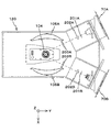
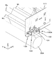
【解決手段】偏向されたレーザ光を受光する受光素子と、レーザ光を反射して受光素子に入射させるミラーとを、ホルダを用いて一体的に保持する。そして、該ホルダを、光源、偏向器、及び走査光学素子のうちの少なくとも1つを保持するハウジングに固定する。これにより、ミラーに対する受光素子の相対位置関係が一定に維持されるとともに、光源、偏向器、及び走査光学素子の少なくとも1つに対する受光素子の相対位置関係も一定に維持される。したがって、受光素子によりレーザ光を精度よく検出することが可能となる。
【選択図】図2
Description
Claims (9)
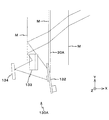
- 被走査面を走査する光走査装置であって、
レーザ光を射出する光源と;
前記光源から射出されたレーザ光を偏向する偏向器と;
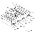
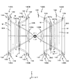
偏向されたレーザ光を前記被走査面に導く複数の走査光学素子と;
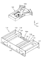
前記光源、前記偏向器、及び前記走査光学素子のうちの少なくとも1つを保持するハウジングと;
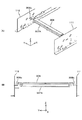
偏向されたレーザ光を受光する受光素子と;
前記偏向されたレーザ光を前記受光素子へ導くミラーと;
前記ハウジングに設けられ、前記受光素子と前記ミラーとを一体的に保持するホルダと;を備える光走査装置。 - 前記ハウジングは、前記光源及び前記偏向器のうちの少なくとも1つを保持する第1ユニットと;
前記走査光学素子を保持する第2ユニットと:を備える請求項1に記載の光走査装置。 - 前記第2ユニットは、プレス加工により形成された板部材を含み、前記ホルダは前記板部材の打ち抜き面により位置決めされている請求項2に記載の光走査装置。
- 前記レーザ光は、前記板部材に設けられた開口部を介して、前記受光素子へ導かれる請求項3に記載の光走査装置。
- 前記ミラーの少なくとも一部が前記ハウジングの外部から内部に差し込まれている請求項1〜4のいずれか一項に記載の光走査装置。
- 前記複数の走査光学素子のうち、最も前記被走査面に近い走査光学素子を通過したレーザ光を分離する分離素子を更に備え、
前記ミラーは前記分離素子に分離されたレーザ光を前記受光素子へ導く請求項1〜5のいずれか一項に記載の光走査装置。 - 前記偏向器は所定の軸回りに回転し、前記ミラーに反射されたレーザ光の光路は、前記軸に直交する請求項6に記載の光走査装置。
- 前記ホルダは、前記走査光学素子のいずれかを保持する請求項1〜7のいずれか一項に記載の光走査装置。
- 画像に関する情報から得られる潜像に基づいて形成されたトナー像を、記録媒体に定着させることにより、画像を形成する画像形成装置であって、
請求項1〜8のいずれか一項に記載の光走査装置と;
前記光走査装置により潜像が形成される感光体と;
前記感光体の被走査面に形成された潜像を顕像化する現像装置と;
前記現像手段により顕像化されたトナー像を前記記録媒体に定着させる転写装置と;を備える画像形成装置。
Priority Applications (2)
| Application Number | Priority Date | Filing Date | Title |
|---|---|---|---|
| JP2008170643A JP5038239B2 (ja) | 2008-06-30 | 2008-06-30 | 光走査装置及び画像形成装置 |
| US12/490,437 US8174747B2 (en) | 2008-06-30 | 2009-06-24 | Optical scanning apparatus and image forming apparatus |
Applications Claiming Priority (1)
| Application Number | Priority Date | Filing Date | Title |
|---|---|---|---|
| JP2008170643A JP5038239B2 (ja) | 2008-06-30 | 2008-06-30 | 光走査装置及び画像形成装置 |
Publications (2)
| Publication Number | Publication Date |
|---|---|
| JP2010008902A true JP2010008902A (ja) | 2010-01-14 |
| JP5038239B2 JP5038239B2 (ja) | 2012-10-03 |
Family
ID=41447043
Family Applications (1)
| Application Number | Title | Priority Date | Filing Date |
|---|---|---|---|
| JP2008170643A Expired - Fee Related JP5038239B2 (ja) | 2008-06-30 | 2008-06-30 | 光走査装置及び画像形成装置 |
Country Status (2)
| Country | Link |
|---|---|
| US (1) | US8174747B2 (ja) |
| JP (1) | JP5038239B2 (ja) |
Cited By (3)
| Publication number | Priority date | Publication date | Assignee | Title |
|---|---|---|---|---|
| JP2011170027A (ja) * | 2010-02-17 | 2011-09-01 | Ricoh Co Ltd | 光学ハウジング、光走査装置及び画像形成装置 |
| US8508808B2 (en) | 2008-02-28 | 2013-08-13 | Ricoh Company, Ltd. | Optical scanning and image forming apparatus with a free-sliding unit for thermal expansion |
| JP2016212429A (ja) * | 2016-07-13 | 2016-12-15 | シャープ株式会社 | 光走査装置、及びそれを備えた画像形成装置 |
Families Citing this family (12)
| Publication number | Priority date | Publication date | Assignee | Title |
|---|---|---|---|---|
| JP5494961B2 (ja) | 2010-06-17 | 2014-05-21 | 株式会社リコー | 光走査装置及び画像形成装置 |
| JP5637494B2 (ja) | 2010-08-20 | 2014-12-10 | 株式会社リコー | 光走査装置及び画像形成装置 |
| US8723908B2 (en) * | 2011-01-13 | 2014-05-13 | Kabushiki Kaisha Toshiba | Optical scanning device including plural lenses and image forming apparatus |
| JP2013178496A (ja) | 2012-02-06 | 2013-09-09 | Ricoh Co Ltd | 光走査装置及び画像形成装置 |
| JP5976495B2 (ja) * | 2012-10-17 | 2016-08-23 | シャープ株式会社 | 光走査装置、及びそれを備えた画像形成装置 |
| JP6127222B2 (ja) * | 2014-11-26 | 2017-05-10 | 京セラドキュメントソリューションズ株式会社 | 光走査装置及びそれを備えた画像形成装置 |
| CN108885338B (zh) * | 2016-04-14 | 2021-01-08 | 京瓷办公信息系统株式会社 | 光扫描装置及具有该光扫描装置的图像形成装置 |
| JP2019105804A (ja) * | 2017-12-14 | 2019-06-27 | 株式会社東芝 | 光走査装置及び画像形成装置 |
| US12332578B2 (en) * | 2022-03-25 | 2025-06-17 | Toshiba Tec Kabushiki Kaisha | Optical scanning device |
| JP2024021978A (ja) * | 2022-08-05 | 2024-02-16 | キヤノン株式会社 | 光走査装置及び画像形成装置 |
| JP2025143707A (ja) * | 2024-03-19 | 2025-10-02 | ブラザー工業株式会社 | 画像形成装置 |
| JP2025144576A (ja) * | 2024-03-20 | 2025-10-03 | ブラザー工業株式会社 | 画像形成装置 |
Citations (3)
| Publication number | Priority date | Publication date | Assignee | Title |
|---|---|---|---|---|
| JPH07140407A (ja) * | 1993-11-15 | 1995-06-02 | Ricoh Co Ltd | 光走査光学系 |
| JPH07318837A (ja) * | 1994-05-19 | 1995-12-08 | Canon Inc | 走査光学装置 |
| JP2005091927A (ja) * | 2003-09-18 | 2005-04-07 | Ricoh Co Ltd | 光走査装置および画像形成装置 |
Family Cites Families (36)
| Publication number | Priority date | Publication date | Assignee | Title |
|---|---|---|---|---|
| US5208612A (en) * | 1989-12-06 | 1993-05-04 | Ricoh Company, Ltd. | Image recording apparatus constituting of selectable units |
| JPH1058738A (ja) * | 1996-08-19 | 1998-03-03 | Ricoh Co Ltd | 光書込装置 |
| JP4774157B2 (ja) * | 2000-04-13 | 2011-09-14 | 株式会社リコー | マルチビーム光源装置及び光走査装置 |
| US6771300B2 (en) * | 2001-03-07 | 2004-08-03 | Ricoh Company, Ltd. | Multi-beam scanning device |
| US7206014B2 (en) * | 2001-07-24 | 2007-04-17 | Ricoh Company, Ltd. | Multi-beam pitch adjusting apparatus and image forming apparatus |
| US7050082B2 (en) * | 2002-01-23 | 2006-05-23 | Ricoh Company, Ltd. | Image forming system employing effective optical scan-line control device |
| US7333254B2 (en) * | 2002-03-15 | 2008-02-19 | Ricoh Company, Ltd. | Optical scanning apparatus, illuminant apparatus and image forming apparatus |
| US7532227B2 (en) * | 2002-07-02 | 2009-05-12 | Ricoh Company, Ltd. | Optical scanner and image forming apparatus |
| US7145589B2 (en) * | 2002-07-12 | 2006-12-05 | Ricoh Company, Ltd. | Light scanning apparatus having a liquid crystal deflector and image forming apparatus using the same |
| JP2004109663A (ja) * | 2002-09-19 | 2004-04-08 | Ricoh Co Ltd | 光源装置、光走査装置及び画像形成装置 |
| US7450274B2 (en) * | 2003-05-07 | 2008-11-11 | Ricoh Company, Ltd. | Optical scanning apparatus, image forming apparatus, and beam positioning method |
| JP4445234B2 (ja) | 2003-09-19 | 2010-04-07 | 株式会社リコー | 光走査装置および画像形成装置 |
| US7403316B2 (en) * | 2004-01-14 | 2008-07-22 | Ricoh Company, Ltd. | Optical scanning device, image forming apparatus and liquid crystal device driving method |
| JP4373800B2 (ja) | 2004-01-26 | 2009-11-25 | 株式会社リコー | 光走査装置、カラー画像形成装置及びレーザビームの検出方法 |
| US7151557B2 (en) * | 2004-03-19 | 2006-12-19 | Lexmark International, Inc. | Collimation assembly for adjusting laser light sources in a multi-beamed laser scanning unit |
| US7528856B2 (en) * | 2004-07-23 | 2009-05-05 | Brother Kogyo Kabushiki Kaisha | Image forming apparatus, optical scanning device and manufacturing method of optical scanning device |
| JP2006126506A (ja) | 2004-10-28 | 2006-05-18 | Ricoh Co Ltd | 光走査装置、および画像形成装置 |
| US7684100B2 (en) * | 2004-11-26 | 2010-03-23 | Ricoh Company, Ltd. | Optical-element holding device, method of adjusting shape of optical element, optical-element shape adjusting device, method of correcting scanning line variation, optical scanning device, and image forming apparatus |
| JP4828838B2 (ja) | 2005-02-21 | 2011-11-30 | 株式会社リコー | 光走査装置の製造方法 |
| JP2006243312A (ja) | 2005-03-03 | 2006-09-14 | Ricoh Co Ltd | 光走査装置と画像形成装置 |
| US20060209171A1 (en) * | 2005-03-15 | 2006-09-21 | Kabushiki Kaisha Toshiba | Optical beam scanning device and image forming apparatus |
| JP4675247B2 (ja) * | 2005-04-20 | 2011-04-20 | 株式会社リコー | 走査光学系、光走査装置及び画像形成装置 |
| JP2006323157A (ja) * | 2005-05-19 | 2006-11-30 | Sharp Corp | 光走査装置及び画像形成装置 |
| JP4801410B2 (ja) * | 2005-10-07 | 2011-10-26 | 株式会社リコー | 光走査装置及び画像形成装置 |
| JP5597906B2 (ja) * | 2005-11-30 | 2014-10-01 | 株式会社リコー | 光走査装置および画像形成装置 |
| JP4921808B2 (ja) * | 2006-02-20 | 2012-04-25 | 株式会社東芝 | 露光装置における光源ユニットおよび露光装置における光軸調整方法 |
| JP2007226130A (ja) * | 2006-02-27 | 2007-09-06 | Ricoh Co Ltd | 光走査装置、画像形成装置、及び位相変調方法 |
| JP4928158B2 (ja) * | 2006-05-26 | 2012-05-09 | キヤノン株式会社 | 走査露光装置及び画像形成装置 |
| US7417662B2 (en) * | 2006-09-12 | 2008-08-26 | Xerox Corporation | Sensor module docking arrangement with multiple degrees of freedom constraint |
| JP4917925B2 (ja) * | 2006-09-15 | 2012-04-18 | 株式会社リコー | 光走査装置及びカラー画像形成装置 |
| JP4922790B2 (ja) * | 2007-03-06 | 2012-04-25 | 株式会社リコー | 光走査装置および画像形成装置 |
| JP4859132B2 (ja) * | 2007-03-28 | 2012-01-25 | 株式会社リコー | 光源装置、光走査装置及び画像形成装置 |
| KR101335997B1 (ko) * | 2007-05-02 | 2013-12-04 | 삼성전자주식회사 | 결상렌즈 어셈블리와, 이를 가지는 광주사유닛 및화상형성장치 |
| JP5316747B2 (ja) | 2007-08-31 | 2013-10-16 | 株式会社リコー | 光源装置、光走査装置及び画像形成装置 |
| JP2009053401A (ja) * | 2007-08-27 | 2009-03-12 | Ricoh Co Ltd | 長尺光学素子の保持機構、光走査装置および画像形成装置 |
| US7710445B2 (en) * | 2007-08-31 | 2010-05-04 | Ricoh Company, Ltd. | Light source unit, optical scan apparatus, and image formation apparatus |
-
2008
- 2008-06-30 JP JP2008170643A patent/JP5038239B2/ja not_active Expired - Fee Related
-
2009
- 2009-06-24 US US12/490,437 patent/US8174747B2/en not_active Expired - Fee Related
Patent Citations (3)
| Publication number | Priority date | Publication date | Assignee | Title |
|---|---|---|---|---|
| JPH07140407A (ja) * | 1993-11-15 | 1995-06-02 | Ricoh Co Ltd | 光走査光学系 |
| JPH07318837A (ja) * | 1994-05-19 | 1995-12-08 | Canon Inc | 走査光学装置 |
| JP2005091927A (ja) * | 2003-09-18 | 2005-04-07 | Ricoh Co Ltd | 光走査装置および画像形成装置 |
Cited By (3)
| Publication number | Priority date | Publication date | Assignee | Title |
|---|---|---|---|---|
| US8508808B2 (en) | 2008-02-28 | 2013-08-13 | Ricoh Company, Ltd. | Optical scanning and image forming apparatus with a free-sliding unit for thermal expansion |
| JP2011170027A (ja) * | 2010-02-17 | 2011-09-01 | Ricoh Co Ltd | 光学ハウジング、光走査装置及び画像形成装置 |
| JP2016212429A (ja) * | 2016-07-13 | 2016-12-15 | シャープ株式会社 | 光走査装置、及びそれを備えた画像形成装置 |
Also Published As
| Publication number | Publication date |
|---|---|
| US20090323147A1 (en) | 2009-12-31 |
| US8174747B2 (en) | 2012-05-08 |
| JP5038239B2 (ja) | 2012-10-03 |
Similar Documents
| Publication | Publication Date | Title |
|---|---|---|
| JP5038239B2 (ja) | 光走査装置及び画像形成装置 | |
| EP2862721A1 (en) | Light scanning unit and image forming apparatus employing the same | |
| JP4480075B2 (ja) | 光書き込み装置及び画像形成装置 | |
| JP2008268683A (ja) | 光走査装置及び画像形成装置 | |
| US8717656B2 (en) | Optical scanning device | |
| JP2008242196A (ja) | 光源装置、光走査装置及び画像形成装置 | |
| JP6489410B2 (ja) | 光走査装置および画像形成装置 | |
| JP5108697B2 (ja) | 光走査装置 | |
| JP5142372B2 (ja) | ミラー、光走査装置及び画像形成装置 | |
| JP2011048085A (ja) | 走査光学装置及び電子写真画像形成装置 | |
| US8717640B2 (en) | Optical scanner and image forming apparatus including same | |
| JP5316747B2 (ja) | 光源装置、光走査装置及び画像形成装置 | |
| JP4818070B2 (ja) | 走査式光学装置及び画像形成装置 | |
| JP5224047B2 (ja) | 光走査装置、ビームピッチ調整方法及び画像形成装置 | |
| JP5326951B2 (ja) | 光走査装置及び画像形成装置 | |
| JP2012150132A (ja) | 発光素子の調整固定構造及び光走査装置及び画像形成装置 | |
| JP5063170B2 (ja) | 光学走査装置及び画像形成装置 | |
| US10120299B2 (en) | Light scanning device with lens holder and image forming apparatus | |
| JP2003185954A (ja) | 走査光学系および画像形成装置 | |
| JP5257723B2 (ja) | 光走査装置及び画像形成装置 | |
| JP2008112041A5 (ja) | ||
| JP2007304166A (ja) | 光学走査装置 | |
| US11914139B2 (en) | Scanning optical apparatus and image forming apparatus | |
| JP4822542B2 (ja) | 光走査装置及び画像形成装置 | |
| JP4695400B2 (ja) | 反射ミラーの支持構造および光書込装置および画像形成装置 |
Legal Events
| Date | Code | Title | Description |
|---|---|---|---|
| A621 | Written request for application examination |
Free format text: JAPANESE INTERMEDIATE CODE: A621 Effective date: 20110112 |
|
| A977 | Report on retrieval |
Free format text: JAPANESE INTERMEDIATE CODE: A971007 Effective date: 20120327 |
|
| A131 | Notification of reasons for refusal |
Free format text: JAPANESE INTERMEDIATE CODE: A131 Effective date: 20120403 |
|
| A521 | Request for written amendment filed |
Free format text: JAPANESE INTERMEDIATE CODE: A523 Effective date: 20120529 |
|
| TRDD | Decision of grant or rejection written | ||
| A01 | Written decision to grant a patent or to grant a registration (utility model) |
Free format text: JAPANESE INTERMEDIATE CODE: A01 Effective date: 20120620 |
|
| A01 | Written decision to grant a patent or to grant a registration (utility model) |
Free format text: JAPANESE INTERMEDIATE CODE: A01 |
|
| A61 | First payment of annual fees (during grant procedure) |
Free format text: JAPANESE INTERMEDIATE CODE: A61 Effective date: 20120705 |
|
| FPAY | Renewal fee payment (event date is renewal date of database) |
Free format text: PAYMENT UNTIL: 20150713 Year of fee payment: 3 |
|
| R150 | Certificate of patent or registration of utility model |
Ref document number: 5038239 Country of ref document: JP Free format text: JAPANESE INTERMEDIATE CODE: R150 Free format text: JAPANESE INTERMEDIATE CODE: R150 |
|
| LAPS | Cancellation because of no payment of annual fees |