JP2006352085A - 波長変換型半導体発光デバイス - Google Patents
波長変換型半導体発光デバイス Download PDFInfo
- Publication number
- JP2006352085A JP2006352085A JP2006109168A JP2006109168A JP2006352085A JP 2006352085 A JP2006352085 A JP 2006352085A JP 2006109168 A JP2006109168 A JP 2006109168A JP 2006109168 A JP2006109168 A JP 2006109168A JP 2006352085 A JP2006352085 A JP 2006352085A
- Authority
- JP
- Japan
- Prior art keywords
- light emitting
- phosphor
- ceramic body
- light
- type region
- Prior art date
- Legal status (The legal status is an assumption and is not a legal conclusion. Google has not performed a legal analysis and makes no representation as to the accuracy of the status listed.)
- Granted
Links
Images


Classifications
-
- H—ELECTRICITY
- H01—ELECTRIC ELEMENTS
- H01L—SEMICONDUCTOR DEVICES NOT COVERED BY CLASS H10
- H01L33/00—Semiconductor devices with at least one potential-jump barrier or surface barrier specially adapted for light emission; Processes or apparatus specially adapted for the manufacture or treatment thereof or of parts thereof; Details thereof
- H01L33/48—Semiconductor devices with at least one potential-jump barrier or surface barrier specially adapted for light emission; Processes or apparatus specially adapted for the manufacture or treatment thereof or of parts thereof; Details thereof characterised by the semiconductor body packages
- H01L33/50—Wavelength conversion elements
- H01L33/501—Wavelength conversion elements characterised by the materials, e.g. binder
-
- B—PERFORMING OPERATIONS; TRANSPORTING
- B82—NANOTECHNOLOGY
- B82Y—SPECIFIC USES OR APPLICATIONS OF NANOSTRUCTURES; MEASUREMENT OR ANALYSIS OF NANOSTRUCTURES; MANUFACTURE OR TREATMENT OF NANOSTRUCTURES
- B82Y30/00—Nanotechnology for materials or surface science, e.g. nanocomposites
-
- C—CHEMISTRY; METALLURGY
- C04—CEMENTS; CONCRETE; ARTIFICIAL STONE; CERAMICS; REFRACTORIES
- C04B—LIME, MAGNESIA; SLAG; CEMENTS; COMPOSITIONS THEREOF, e.g. MORTARS, CONCRETE OR LIKE BUILDING MATERIALS; ARTIFICIAL STONE; CERAMICS; REFRACTORIES; TREATMENT OF NATURAL STONE
- C04B35/00—Shaped ceramic products characterised by their composition; Ceramics compositions; Processing powders of inorganic compounds preparatory to the manufacturing of ceramic products
- C04B35/01—Shaped ceramic products characterised by their composition; Ceramics compositions; Processing powders of inorganic compounds preparatory to the manufacturing of ceramic products based on oxide ceramics
- C04B35/44—Shaped ceramic products characterised by their composition; Ceramics compositions; Processing powders of inorganic compounds preparatory to the manufacturing of ceramic products based on oxide ceramics based on aluminates
-
- C—CHEMISTRY; METALLURGY
- C04—CEMENTS; CONCRETE; ARTIFICIAL STONE; CERAMICS; REFRACTORIES
- C04B—LIME, MAGNESIA; SLAG; CEMENTS; COMPOSITIONS THEREOF, e.g. MORTARS, CONCRETE OR LIKE BUILDING MATERIALS; ARTIFICIAL STONE; CERAMICS; REFRACTORIES; TREATMENT OF NATURAL STONE
- C04B35/00—Shaped ceramic products characterised by their composition; Ceramics compositions; Processing powders of inorganic compounds preparatory to the manufacturing of ceramic products
- C04B35/01—Shaped ceramic products characterised by their composition; Ceramics compositions; Processing powders of inorganic compounds preparatory to the manufacturing of ceramic products based on oxide ceramics
- C04B35/495—Shaped ceramic products characterised by their composition; Ceramics compositions; Processing powders of inorganic compounds preparatory to the manufacturing of ceramic products based on oxide ceramics based on vanadium, niobium, tantalum, molybdenum or tungsten oxides or solid solutions thereof with other oxides, e.g. vanadates, niobates, tantalates, molybdates or tungstates
-
- C—CHEMISTRY; METALLURGY
- C04—CEMENTS; CONCRETE; ARTIFICIAL STONE; CERAMICS; REFRACTORIES
- C04B—LIME, MAGNESIA; SLAG; CEMENTS; COMPOSITIONS THEREOF, e.g. MORTARS, CONCRETE OR LIKE BUILDING MATERIALS; ARTIFICIAL STONE; CERAMICS; REFRACTORIES; TREATMENT OF NATURAL STONE
- C04B35/00—Shaped ceramic products characterised by their composition; Ceramics compositions; Processing powders of inorganic compounds preparatory to the manufacturing of ceramic products
- C04B35/622—Forming processes; Processing powders of inorganic compounds preparatory to the manufacturing of ceramic products
- C04B35/626—Preparing or treating the powders individually or as batches ; preparing or treating macroscopic reinforcing agents for ceramic products, e.g. fibres; mechanical aspects section B
- C04B35/62605—Treating the starting powders individually or as mixtures
- C04B35/62645—Thermal treatment of powders or mixtures thereof other than sintering
- C04B35/6268—Thermal treatment of powders or mixtures thereof other than sintering characterised by the applied pressure or type of atmosphere, e.g. in vacuum, hydrogen or a specific oxygen pressure
-
- C—CHEMISTRY; METALLURGY
- C04—CEMENTS; CONCRETE; ARTIFICIAL STONE; CERAMICS; REFRACTORIES
- C04B—LIME, MAGNESIA; SLAG; CEMENTS; COMPOSITIONS THEREOF, e.g. MORTARS, CONCRETE OR LIKE BUILDING MATERIALS; ARTIFICIAL STONE; CERAMICS; REFRACTORIES; TREATMENT OF NATURAL STONE
- C04B35/00—Shaped ceramic products characterised by their composition; Ceramics compositions; Processing powders of inorganic compounds preparatory to the manufacturing of ceramic products
- C04B35/622—Forming processes; Processing powders of inorganic compounds preparatory to the manufacturing of ceramic products
- C04B35/626—Preparing or treating the powders individually or as batches ; preparing or treating macroscopic reinforcing agents for ceramic products, e.g. fibres; mechanical aspects section B
- C04B35/628—Coating the powders or the macroscopic reinforcing agents
- C04B35/62802—Powder coating materials
- C04B35/62805—Oxide ceramics
- C04B35/62807—Silica or silicates
-
- C—CHEMISTRY; METALLURGY
- C04—CEMENTS; CONCRETE; ARTIFICIAL STONE; CERAMICS; REFRACTORIES
- C04B—LIME, MAGNESIA; SLAG; CEMENTS; COMPOSITIONS THEREOF, e.g. MORTARS, CONCRETE OR LIKE BUILDING MATERIALS; ARTIFICIAL STONE; CERAMICS; REFRACTORIES; TREATMENT OF NATURAL STONE
- C04B35/00—Shaped ceramic products characterised by their composition; Ceramics compositions; Processing powders of inorganic compounds preparatory to the manufacturing of ceramic products
- C04B35/622—Forming processes; Processing powders of inorganic compounds preparatory to the manufacturing of ceramic products
- C04B35/626—Preparing or treating the powders individually or as batches ; preparing or treating macroscopic reinforcing agents for ceramic products, e.g. fibres; mechanical aspects section B
- C04B35/628—Coating the powders or the macroscopic reinforcing agents
- C04B35/62802—Powder coating materials
- C04B35/62805—Oxide ceramics
- C04B35/62813—Alumina or aluminates
-
- C—CHEMISTRY; METALLURGY
- C04—CEMENTS; CONCRETE; ARTIFICIAL STONE; CERAMICS; REFRACTORIES
- C04B—LIME, MAGNESIA; SLAG; CEMENTS; COMPOSITIONS THEREOF, e.g. MORTARS, CONCRETE OR LIKE BUILDING MATERIALS; ARTIFICIAL STONE; CERAMICS; REFRACTORIES; TREATMENT OF NATURAL STONE
- C04B35/00—Shaped ceramic products characterised by their composition; Ceramics compositions; Processing powders of inorganic compounds preparatory to the manufacturing of ceramic products
- C04B35/622—Forming processes; Processing powders of inorganic compounds preparatory to the manufacturing of ceramic products
- C04B35/64—Burning or sintering processes
- C04B35/645—Pressure sintering
-
- C—CHEMISTRY; METALLURGY
- C04—CEMENTS; CONCRETE; ARTIFICIAL STONE; CERAMICS; REFRACTORIES
- C04B—LIME, MAGNESIA; SLAG; CEMENTS; COMPOSITIONS THEREOF, e.g. MORTARS, CONCRETE OR LIKE BUILDING MATERIALS; ARTIFICIAL STONE; CERAMICS; REFRACTORIES; TREATMENT OF NATURAL STONE
- C04B37/00—Joining burned ceramic articles with other burned ceramic articles or other articles by heating
- C04B37/001—Joining burned ceramic articles with other burned ceramic articles or other articles by heating directly with other burned ceramic articles
-
- C—CHEMISTRY; METALLURGY
- C04—CEMENTS; CONCRETE; ARTIFICIAL STONE; CERAMICS; REFRACTORIES
- C04B—LIME, MAGNESIA; SLAG; CEMENTS; COMPOSITIONS THEREOF, e.g. MORTARS, CONCRETE OR LIKE BUILDING MATERIALS; ARTIFICIAL STONE; CERAMICS; REFRACTORIES; TREATMENT OF NATURAL STONE
- C04B37/00—Joining burned ceramic articles with other burned ceramic articles or other articles by heating
- C04B37/003—Joining burned ceramic articles with other burned ceramic articles or other articles by heating by means of an interlayer consisting of a combination of materials selected from glass, or ceramic material with metals, metal oxides or metal salts
- C04B37/005—Joining burned ceramic articles with other burned ceramic articles or other articles by heating by means of an interlayer consisting of a combination of materials selected from glass, or ceramic material with metals, metal oxides or metal salts consisting of glass or ceramic material
-
- C—CHEMISTRY; METALLURGY
- C04—CEMENTS; CONCRETE; ARTIFICIAL STONE; CERAMICS; REFRACTORIES
- C04B—LIME, MAGNESIA; SLAG; CEMENTS; COMPOSITIONS THEREOF, e.g. MORTARS, CONCRETE OR LIKE BUILDING MATERIALS; ARTIFICIAL STONE; CERAMICS; REFRACTORIES; TREATMENT OF NATURAL STONE
- C04B37/00—Joining burned ceramic articles with other burned ceramic articles or other articles by heating
- C04B37/003—Joining burned ceramic articles with other burned ceramic articles or other articles by heating by means of an interlayer consisting of a combination of materials selected from glass, or ceramic material with metals, metal oxides or metal salts
- C04B37/006—Joining burned ceramic articles with other burned ceramic articles or other articles by heating by means of an interlayer consisting of a combination of materials selected from glass, or ceramic material with metals, metal oxides or metal salts consisting of metals or metal salts
-
- C—CHEMISTRY; METALLURGY
- C04—CEMENTS; CONCRETE; ARTIFICIAL STONE; CERAMICS; REFRACTORIES
- C04B—LIME, MAGNESIA; SLAG; CEMENTS; COMPOSITIONS THEREOF, e.g. MORTARS, CONCRETE OR LIKE BUILDING MATERIALS; ARTIFICIAL STONE; CERAMICS; REFRACTORIES; TREATMENT OF NATURAL STONE
- C04B37/00—Joining burned ceramic articles with other burned ceramic articles or other articles by heating
- C04B37/008—Joining burned ceramic articles with other burned ceramic articles or other articles by heating by means of an interlayer consisting of an organic adhesive, e.g. phenol resin or pitch
-
- C—CHEMISTRY; METALLURGY
- C04—CEMENTS; CONCRETE; ARTIFICIAL STONE; CERAMICS; REFRACTORIES
- C04B—LIME, MAGNESIA; SLAG; CEMENTS; COMPOSITIONS THEREOF, e.g. MORTARS, CONCRETE OR LIKE BUILDING MATERIALS; ARTIFICIAL STONE; CERAMICS; REFRACTORIES; TREATMENT OF NATURAL STONE
- C04B37/00—Joining burned ceramic articles with other burned ceramic articles or other articles by heating
- C04B37/02—Joining burned ceramic articles with other burned ceramic articles or other articles by heating with metallic articles
- C04B37/023—Joining burned ceramic articles with other burned ceramic articles or other articles by heating with metallic articles characterised by the interlayer used
- C04B37/026—Joining burned ceramic articles with other burned ceramic articles or other articles by heating with metallic articles characterised by the interlayer used consisting of metals or metal salts
-
- C—CHEMISTRY; METALLURGY
- C04—CEMENTS; CONCRETE; ARTIFICIAL STONE; CERAMICS; REFRACTORIES
- C04B—LIME, MAGNESIA; SLAG; CEMENTS; COMPOSITIONS THEREOF, e.g. MORTARS, CONCRETE OR LIKE BUILDING MATERIALS; ARTIFICIAL STONE; CERAMICS; REFRACTORIES; TREATMENT OF NATURAL STONE
- C04B2235/00—Aspects relating to ceramic starting mixtures or sintered ceramic products
- C04B2235/02—Composition of constituents of the starting material or of secondary phases of the final product
- C04B2235/30—Constituents and secondary phases not being of a fibrous nature
- C04B2235/32—Metal oxides, mixed metal oxides, or oxide-forming salts thereof, e.g. carbonates, nitrates, (oxy)hydroxides, chlorides
- C04B2235/3217—Aluminum oxide or oxide forming salts thereof, e.g. bauxite, alpha-alumina
-
- C—CHEMISTRY; METALLURGY
- C04—CEMENTS; CONCRETE; ARTIFICIAL STONE; CERAMICS; REFRACTORIES
- C04B—LIME, MAGNESIA; SLAG; CEMENTS; COMPOSITIONS THEREOF, e.g. MORTARS, CONCRETE OR LIKE BUILDING MATERIALS; ARTIFICIAL STONE; CERAMICS; REFRACTORIES; TREATMENT OF NATURAL STONE
- C04B2235/00—Aspects relating to ceramic starting mixtures or sintered ceramic products
- C04B2235/02—Composition of constituents of the starting material or of secondary phases of the final product
- C04B2235/30—Constituents and secondary phases not being of a fibrous nature
- C04B2235/32—Metal oxides, mixed metal oxides, or oxide-forming salts thereof, e.g. carbonates, nitrates, (oxy)hydroxides, chlorides
- C04B2235/3224—Rare earth oxide or oxide forming salts thereof, e.g. scandium oxide
- C04B2235/3225—Yttrium oxide or oxide-forming salts thereof
-
- C—CHEMISTRY; METALLURGY
- C04—CEMENTS; CONCRETE; ARTIFICIAL STONE; CERAMICS; REFRACTORIES
- C04B—LIME, MAGNESIA; SLAG; CEMENTS; COMPOSITIONS THEREOF, e.g. MORTARS, CONCRETE OR LIKE BUILDING MATERIALS; ARTIFICIAL STONE; CERAMICS; REFRACTORIES; TREATMENT OF NATURAL STONE
- C04B2235/00—Aspects relating to ceramic starting mixtures or sintered ceramic products
- C04B2235/02—Composition of constituents of the starting material or of secondary phases of the final product
- C04B2235/30—Constituents and secondary phases not being of a fibrous nature
- C04B2235/32—Metal oxides, mixed metal oxides, or oxide-forming salts thereof, e.g. carbonates, nitrates, (oxy)hydroxides, chlorides
- C04B2235/3224—Rare earth oxide or oxide forming salts thereof, e.g. scandium oxide
- C04B2235/3229—Cerium oxides or oxide-forming salts thereof
-
- C—CHEMISTRY; METALLURGY
- C04—CEMENTS; CONCRETE; ARTIFICIAL STONE; CERAMICS; REFRACTORIES
- C04B—LIME, MAGNESIA; SLAG; CEMENTS; COMPOSITIONS THEREOF, e.g. MORTARS, CONCRETE OR LIKE BUILDING MATERIALS; ARTIFICIAL STONE; CERAMICS; REFRACTORIES; TREATMENT OF NATURAL STONE
- C04B2235/00—Aspects relating to ceramic starting mixtures or sintered ceramic products
- C04B2235/02—Composition of constituents of the starting material or of secondary phases of the final product
- C04B2235/50—Constituents or additives of the starting mixture chosen for their shape or used because of their shape or their physical appearance
- C04B2235/54—Particle size related information
- C04B2235/5418—Particle size related information expressed by the size of the particles or aggregates thereof
- C04B2235/5454—Particle size related information expressed by the size of the particles or aggregates thereof nanometer sized, i.e. below 100 nm
-
- C—CHEMISTRY; METALLURGY
- C04—CEMENTS; CONCRETE; ARTIFICIAL STONE; CERAMICS; REFRACTORIES
- C04B—LIME, MAGNESIA; SLAG; CEMENTS; COMPOSITIONS THEREOF, e.g. MORTARS, CONCRETE OR LIKE BUILDING MATERIALS; ARTIFICIAL STONE; CERAMICS; REFRACTORIES; TREATMENT OF NATURAL STONE
- C04B2237/00—Aspects relating to ceramic laminates or to joining of ceramic articles with other articles by heating
- C04B2237/02—Aspects relating to interlayers, e.g. used to join ceramic articles with other articles by heating
- C04B2237/04—Ceramic interlayers
- C04B2237/06—Oxidic interlayers
- C04B2237/064—Oxidic interlayers based on alumina or aluminates
-
- C—CHEMISTRY; METALLURGY
- C04—CEMENTS; CONCRETE; ARTIFICIAL STONE; CERAMICS; REFRACTORIES
- C04B—LIME, MAGNESIA; SLAG; CEMENTS; COMPOSITIONS THEREOF, e.g. MORTARS, CONCRETE OR LIKE BUILDING MATERIALS; ARTIFICIAL STONE; CERAMICS; REFRACTORIES; TREATMENT OF NATURAL STONE
- C04B2237/00—Aspects relating to ceramic laminates or to joining of ceramic articles with other articles by heating
- C04B2237/02—Aspects relating to interlayers, e.g. used to join ceramic articles with other articles by heating
- C04B2237/04—Ceramic interlayers
- C04B2237/06—Oxidic interlayers
- C04B2237/068—Oxidic interlayers based on refractory oxides, e.g. zirconia
-
- C—CHEMISTRY; METALLURGY
- C04—CEMENTS; CONCRETE; ARTIFICIAL STONE; CERAMICS; REFRACTORIES
- C04B—LIME, MAGNESIA; SLAG; CEMENTS; COMPOSITIONS THEREOF, e.g. MORTARS, CONCRETE OR LIKE BUILDING MATERIALS; ARTIFICIAL STONE; CERAMICS; REFRACTORIES; TREATMENT OF NATURAL STONE
- C04B2237/00—Aspects relating to ceramic laminates or to joining of ceramic articles with other articles by heating
- C04B2237/02—Aspects relating to interlayers, e.g. used to join ceramic articles with other articles by heating
- C04B2237/04—Ceramic interlayers
- C04B2237/08—Non-oxidic interlayers
- C04B2237/083—Carbide interlayers, e.g. silicon carbide interlayers
-
- C—CHEMISTRY; METALLURGY
- C04—CEMENTS; CONCRETE; ARTIFICIAL STONE; CERAMICS; REFRACTORIES
- C04B—LIME, MAGNESIA; SLAG; CEMENTS; COMPOSITIONS THEREOF, e.g. MORTARS, CONCRETE OR LIKE BUILDING MATERIALS; ARTIFICIAL STONE; CERAMICS; REFRACTORIES; TREATMENT OF NATURAL STONE
- C04B2237/00—Aspects relating to ceramic laminates or to joining of ceramic articles with other articles by heating
- C04B2237/02—Aspects relating to interlayers, e.g. used to join ceramic articles with other articles by heating
- C04B2237/10—Glass interlayers, e.g. frit or flux
-
- C—CHEMISTRY; METALLURGY
- C04—CEMENTS; CONCRETE; ARTIFICIAL STONE; CERAMICS; REFRACTORIES
- C04B—LIME, MAGNESIA; SLAG; CEMENTS; COMPOSITIONS THEREOF, e.g. MORTARS, CONCRETE OR LIKE BUILDING MATERIALS; ARTIFICIAL STONE; CERAMICS; REFRACTORIES; TREATMENT OF NATURAL STONE
- C04B2237/00—Aspects relating to ceramic laminates or to joining of ceramic articles with other articles by heating
- C04B2237/02—Aspects relating to interlayers, e.g. used to join ceramic articles with other articles by heating
- C04B2237/12—Metallic interlayers
-
- C—CHEMISTRY; METALLURGY
- C04—CEMENTS; CONCRETE; ARTIFICIAL STONE; CERAMICS; REFRACTORIES
- C04B—LIME, MAGNESIA; SLAG; CEMENTS; COMPOSITIONS THEREOF, e.g. MORTARS, CONCRETE OR LIKE BUILDING MATERIALS; ARTIFICIAL STONE; CERAMICS; REFRACTORIES; TREATMENT OF NATURAL STONE
- C04B2237/00—Aspects relating to ceramic laminates or to joining of ceramic articles with other articles by heating
- C04B2237/30—Composition of layers of ceramic laminates or of ceramic or metallic articles to be joined by heating, e.g. Si substrates
- C04B2237/32—Ceramic
- C04B2237/34—Oxidic
- C04B2237/343—Alumina or aluminates
-
- C—CHEMISTRY; METALLURGY
- C04—CEMENTS; CONCRETE; ARTIFICIAL STONE; CERAMICS; REFRACTORIES
- C04B—LIME, MAGNESIA; SLAG; CEMENTS; COMPOSITIONS THEREOF, e.g. MORTARS, CONCRETE OR LIKE BUILDING MATERIALS; ARTIFICIAL STONE; CERAMICS; REFRACTORIES; TREATMENT OF NATURAL STONE
- C04B2237/00—Aspects relating to ceramic laminates or to joining of ceramic articles with other articles by heating
- C04B2237/30—Composition of layers of ceramic laminates or of ceramic or metallic articles to be joined by heating, e.g. Si substrates
- C04B2237/32—Ceramic
- C04B2237/36—Non-oxidic
- C04B2237/365—Silicon carbide
-
- C—CHEMISTRY; METALLURGY
- C04—CEMENTS; CONCRETE; ARTIFICIAL STONE; CERAMICS; REFRACTORIES
- C04B—LIME, MAGNESIA; SLAG; CEMENTS; COMPOSITIONS THEREOF, e.g. MORTARS, CONCRETE OR LIKE BUILDING MATERIALS; ARTIFICIAL STONE; CERAMICS; REFRACTORIES; TREATMENT OF NATURAL STONE
- C04B2237/00—Aspects relating to ceramic laminates or to joining of ceramic articles with other articles by heating
- C04B2237/30—Composition of layers of ceramic laminates or of ceramic or metallic articles to be joined by heating, e.g. Si substrates
- C04B2237/32—Ceramic
- C04B2237/36—Non-oxidic
- C04B2237/366—Aluminium nitride
-
- C—CHEMISTRY; METALLURGY
- C04—CEMENTS; CONCRETE; ARTIFICIAL STONE; CERAMICS; REFRACTORIES
- C04B—LIME, MAGNESIA; SLAG; CEMENTS; COMPOSITIONS THEREOF, e.g. MORTARS, CONCRETE OR LIKE BUILDING MATERIALS; ARTIFICIAL STONE; CERAMICS; REFRACTORIES; TREATMENT OF NATURAL STONE
- C04B2237/00—Aspects relating to ceramic laminates or to joining of ceramic articles with other articles by heating
- C04B2237/30—Composition of layers of ceramic laminates or of ceramic or metallic articles to be joined by heating, e.g. Si substrates
- C04B2237/32—Ceramic
- C04B2237/36—Non-oxidic
- C04B2237/368—Silicon nitride
-
- C—CHEMISTRY; METALLURGY
- C04—CEMENTS; CONCRETE; ARTIFICIAL STONE; CERAMICS; REFRACTORIES
- C04B—LIME, MAGNESIA; SLAG; CEMENTS; COMPOSITIONS THEREOF, e.g. MORTARS, CONCRETE OR LIKE BUILDING MATERIALS; ARTIFICIAL STONE; CERAMICS; REFRACTORIES; TREATMENT OF NATURAL STONE
- C04B2237/00—Aspects relating to ceramic laminates or to joining of ceramic articles with other articles by heating
- C04B2237/50—Processing aspects relating to ceramic laminates or to the joining of ceramic articles with other articles by heating
- C04B2237/52—Pre-treatment of the joining surfaces, e.g. cleaning, machining
- C04B2237/525—Pre-treatment of the joining surfaces, e.g. cleaning, machining by heating
-
- C—CHEMISTRY; METALLURGY
- C04—CEMENTS; CONCRETE; ARTIFICIAL STONE; CERAMICS; REFRACTORIES
- C04B—LIME, MAGNESIA; SLAG; CEMENTS; COMPOSITIONS THEREOF, e.g. MORTARS, CONCRETE OR LIKE BUILDING MATERIALS; ARTIFICIAL STONE; CERAMICS; REFRACTORIES; TREATMENT OF NATURAL STONE
- C04B2237/00—Aspects relating to ceramic laminates or to joining of ceramic articles with other articles by heating
- C04B2237/50—Processing aspects relating to ceramic laminates or to the joining of ceramic articles with other articles by heating
- C04B2237/70—Forming laminates or joined articles comprising layers of a specific, unusual thickness
- C04B2237/704—Forming laminates or joined articles comprising layers of a specific, unusual thickness of one or more of the ceramic layers or articles
-
- C—CHEMISTRY; METALLURGY
- C04—CEMENTS; CONCRETE; ARTIFICIAL STONE; CERAMICS; REFRACTORIES
- C04B—LIME, MAGNESIA; SLAG; CEMENTS; COMPOSITIONS THEREOF, e.g. MORTARS, CONCRETE OR LIKE BUILDING MATERIALS; ARTIFICIAL STONE; CERAMICS; REFRACTORIES; TREATMENT OF NATURAL STONE
- C04B2237/00—Aspects relating to ceramic laminates or to joining of ceramic articles with other articles by heating
- C04B2237/50—Processing aspects relating to ceramic laminates or to the joining of ceramic articles with other articles by heating
- C04B2237/70—Forming laminates or joined articles comprising layers of a specific, unusual thickness
- C04B2237/708—Forming laminates or joined articles comprising layers of a specific, unusual thickness of one or more of the interlayers
-
- C—CHEMISTRY; METALLURGY
- C04—CEMENTS; CONCRETE; ARTIFICIAL STONE; CERAMICS; REFRACTORIES
- C04B—LIME, MAGNESIA; SLAG; CEMENTS; COMPOSITIONS THEREOF, e.g. MORTARS, CONCRETE OR LIKE BUILDING MATERIALS; ARTIFICIAL STONE; CERAMICS; REFRACTORIES; TREATMENT OF NATURAL STONE
- C04B2237/00—Aspects relating to ceramic laminates or to joining of ceramic articles with other articles by heating
- C04B2237/50—Processing aspects relating to ceramic laminates or to the joining of ceramic articles with other articles by heating
- C04B2237/76—Forming laminates or joined articles comprising at least one member in the form other than a sheet or disc, e.g. two tubes or a tube and a sheet or disc
-
- H—ELECTRICITY
- H01—ELECTRIC ELEMENTS
- H01L—SEMICONDUCTOR DEVICES NOT COVERED BY CLASS H10
- H01L2224/00—Indexing scheme for arrangements for connecting or disconnecting semiconductor or solid-state bodies and methods related thereto as covered by H01L24/00
- H01L2224/01—Means for bonding being attached to, or being formed on, the surface to be connected, e.g. chip-to-package, die-attach, "first-level" interconnects; Manufacturing methods related thereto
- H01L2224/02—Bonding areas; Manufacturing methods related thereto
- H01L2224/04—Structure, shape, material or disposition of the bonding areas prior to the connecting process
- H01L2224/05—Structure, shape, material or disposition of the bonding areas prior to the connecting process of an individual bonding area
- H01L2224/0554—External layer
- H01L2224/0556—Disposition
- H01L2224/05568—Disposition the whole external layer protruding from the surface
-
- H—ELECTRICITY
- H01—ELECTRIC ELEMENTS
- H01L—SEMICONDUCTOR DEVICES NOT COVERED BY CLASS H10
- H01L2224/00—Indexing scheme for arrangements for connecting or disconnecting semiconductor or solid-state bodies and methods related thereto as covered by H01L24/00
- H01L2224/01—Means for bonding being attached to, or being formed on, the surface to be connected, e.g. chip-to-package, die-attach, "first-level" interconnects; Manufacturing methods related thereto
- H01L2224/02—Bonding areas; Manufacturing methods related thereto
- H01L2224/04—Structure, shape, material or disposition of the bonding areas prior to the connecting process
- H01L2224/05—Structure, shape, material or disposition of the bonding areas prior to the connecting process of an individual bonding area
- H01L2224/0554—External layer
- H01L2224/05573—Single external layer
-
- H—ELECTRICITY
- H01—ELECTRIC ELEMENTS
- H01L—SEMICONDUCTOR DEVICES NOT COVERED BY CLASS H10
- H01L2224/00—Indexing scheme for arrangements for connecting or disconnecting semiconductor or solid-state bodies and methods related thereto as covered by H01L24/00
- H01L2224/01—Means for bonding being attached to, or being formed on, the surface to be connected, e.g. chip-to-package, die-attach, "first-level" interconnects; Manufacturing methods related thereto
- H01L2224/10—Bump connectors; Manufacturing methods related thereto
- H01L2224/12—Structure, shape, material or disposition of the bump connectors prior to the connecting process
- H01L2224/14—Structure, shape, material or disposition of the bump connectors prior to the connecting process of a plurality of bump connectors
-
- H—ELECTRICITY
- H01—ELECTRIC ELEMENTS
- H01L—SEMICONDUCTOR DEVICES NOT COVERED BY CLASS H10
- H01L2924/00—Indexing scheme for arrangements or methods for connecting or disconnecting semiconductor or solid-state bodies as covered by H01L24/00
- H01L2924/0001—Technical content checked by a classifier
- H01L2924/00014—Technical content checked by a classifier the subject-matter covered by the group, the symbol of which is combined with the symbol of this group, being disclosed without further technical details
-
- H—ELECTRICITY
- H01—ELECTRIC ELEMENTS
- H01L—SEMICONDUCTOR DEVICES NOT COVERED BY CLASS H10
- H01L2924/00—Indexing scheme for arrangements or methods for connecting or disconnecting semiconductor or solid-state bodies as covered by H01L24/00
- H01L2924/0001—Technical content checked by a classifier
- H01L2924/0002—Not covered by any one of groups H01L24/00, H01L24/00 and H01L2224/00
-
- H—ELECTRICITY
- H01—ELECTRIC ELEMENTS
- H01L—SEMICONDUCTOR DEVICES NOT COVERED BY CLASS H10
- H01L33/00—Semiconductor devices with at least one potential-jump barrier or surface barrier specially adapted for light emission; Processes or apparatus specially adapted for the manufacture or treatment thereof or of parts thereof; Details thereof
- H01L33/005—Processes
- H01L33/0093—Wafer bonding; Removal of the growth substrate
-
- H—ELECTRICITY
- H01—ELECTRIC ELEMENTS
- H01L—SEMICONDUCTOR DEVICES NOT COVERED BY CLASS H10
- H01L33/00—Semiconductor devices with at least one potential-jump barrier or surface barrier specially adapted for light emission; Processes or apparatus specially adapted for the manufacture or treatment thereof or of parts thereof; Details thereof
- H01L33/02—Semiconductor devices with at least one potential-jump barrier or surface barrier specially adapted for light emission; Processes or apparatus specially adapted for the manufacture or treatment thereof or of parts thereof; Details thereof characterised by the semiconductor bodies
- H01L33/08—Semiconductor devices with at least one potential-jump barrier or surface barrier specially adapted for light emission; Processes or apparatus specially adapted for the manufacture or treatment thereof or of parts thereof; Details thereof characterised by the semiconductor bodies with a plurality of light emitting regions, e.g. laterally discontinuous light emitting layer or photoluminescent region integrated within the semiconductor body
Abstract
【解決手段】発光領域から蛍光体中に光を効率的に取り出すことを目的として、蛍光体などの材料が、n型領域とp型領域の間に配置された発光領域を含む半導体構造体に、光学的に結合される。蛍光体は、半導体構造体の表面に直接接触した蛍光体粒、又は、半導体構造体又はその上に半導体構造体が成長させられる薄い核生成構造体に接合されたセラミック蛍光体とすることができる。蛍光体は高吸収性で高効率であることが好ましい。半導体構造体がそのような高効率、高吸収性の蛍光体中に光を放射すると、蛍光体は構造体から効率的に光を取り出し、従来技術に存在している光学的損失を低減する。
【選択図】図5
Description
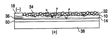
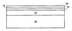
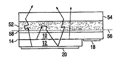
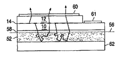
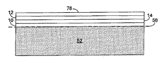
10:半導体層
12:半導体層
14:活性領域
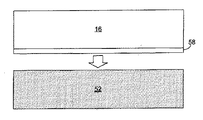
16:透明上層(成長基板)
18、20、60、61:コンタクト
22、24:接続
26、28:基板コンタクト
30:蛍光体層
32:光学的結合媒体
34:蛍光体粒(蛍光体層)
36:エピタキシャル層
38:ホスト基板
50:金属層
52:セラミック蛍光体層
54、62:反射鏡
56:接合材
58:核生成層
72:水素注入部
76:準備層
78:再成長p+材料
100:放熱スラグ
102:反射キャップ
103:熱伝導性補助キャップ
104:発光デバイス・ダイ
105:充填プラスチック材料
106:リードフレーム
108:カバー
130:半導体構造体
132:パッケージ素子
134:金属インターフェース
Claims (37)
- セラミック体蛍光体が第一ピーク波長の光を吸収し第二ピーク波長の光を放射するように形成された蛍光体を含むセラミック体を準備するステップと、
前記セラミック体を核生成構造体に接合するステップと、
前記核生成構造体上に、n型領域とp型領域との間に配置されて前記第一ピーク波長の光を放射するように形成された発光領域を有する半導体構造体を成長させるステップと、
を含み、
前記核生成構造体は、成長前における厚さが100ミクロンより小さいことを特徴とする方法。 - 前記接合ステップが、実質的に金属又は接着剤のない接合を形成するステップを含むことを特徴とする請求項1に記載の方法。
- 前記接合ステップが、前記セラミック体と前記核生成構造体とを500℃より高い温度及び5psiより高い圧力において互いに圧着するステップを含むことを特徴とする請求項1に記載の方法。
- 前記核生成構造体が、GaN,AlN,SiC,及びAl2O3の群から選択されることを特徴とする請求項1に記載の方法。
- 基板上に形成された核生成構造体を準備するステップと、
接合後に前記基板を除去するステップと、
をさらに含むことを特徴とする請求項1に記載の方法。 - 前記n型領域及び前記p型領域の両方の一部を露出させるために、前記半導体構造体をエッチングするステップと、
前記n型領域及び前記p型領域のそれぞれの上にコンタクトを形成するステップと、
をさらに含むことを特徴とする請求項1に記載の方法。 - 前記コンタクトの少なくとも1つが反射性であることを特徴とする請求項6に記載の方法。
- 前記セラミック体をレンズに成型するステップをさらに含むことを特徴とする請求項1に記載の方法。
- 前記セラミック体の表面をテクスチャ加工又は粗面化するステップをさらに含むことを特徴とする請求項1に記載の方法。
- 前記セラミック体が透明であることを特徴とする請求項1に記載の方法。
- 前記セラミック体が不透明であることを特徴とする請求項1に記載の方法。
- 前記核生成構造体は、成長前における厚さが10ミクロンより小さいことを特徴とする請求項1に記載の方法。
- 前記核生成構造体は、成長前における厚さが1ミクロンより小さいことを特徴とする請求項1に記載の方法。
- 前記核生成構造体と前記セラミック構造体との間に接合層を生成するステップをさらに含むことを特徴とする請求項1に記載の方法。
- 第一ピーク波長の光を吸収し第二ピーク波長の光を放射するように形成された蛍光体を含むセラミック体を準備するステップと、
成長基板上に形成され、第一ピーク波長の光を放射するように形成された発光領域がn型領域とp型領域との間に配置された半導体構造体を準備するステップと、
前記セラミック体を前記半導体構造体の表面に接合するステップと、
接合後に成長基板を除去するステップと、
を含むことを特徴とする方法。 - 前記n型領域を成長させる前に前記p型領域が前記成長基板上に成長させられることを特徴とする請求項15に記載の方法。
- 前記成長基板の除去後に前記半導体構造体をアニールするステップをさらに含むことを特徴とする請求項16に記載の方法。
- 前記セラミック体に接合される前記半導体構造体の表面がn−型領域の表面であることを特徴とする請求項15に記載の方法。
- 前記半導体構造体と前記セラミック体との間に接合層を生成するステップをさらに含むことを特徴とする請求項15に記載の方法。
- n−型領域とp−型領域の間に挟まれた発光領域を有する複数の層を含む半導体構造体と、
前記複数の層の1つに直接接触する発光性材料と、
を備え、
前記発光領域によって放射される光の波長において、前記発光性材料の屈折率の虚数部kが0.01より大きいことを特徴とする発光デバイス。 - kが0.1より大きいことを特徴とする請求項20に記載の発光デバイス。
- 前記発光領域がIII−窒化物材料を含むことを特徴とする請求項20に記載の発光デバイス。
- 前記発光性材料が蛍光体を含むことを特徴とする請求項20に記載の発光デバイス。
- 前記発光性材料がセラミック蛍光体を含むことを特徴とする請求項23に記載の発光デバイス。
- 前記発光性材料が蛍光体粒を含むことを特徴とする請求項23に記載の発光デバイス。
- 前記蛍光体粒の上に配置され、1.7より大きな屈折率をもつ透明材料をさらに含むことを特徴とする請求項25に記載の発光デバイス。
- 前記透明材料がガラスを含むことを特徴とする請求項26に記載の発光デバイス。
- 前記ガラスがゾルーゲルガラスを含むことを特徴とする請求項27に記載の発光デバイス。
- 前記透明材料中に配置され、約2nmから約50nmまでの間の直径を有するナノ粒子をさらに含むことを特徴とする請求項26に記載の発光デバイス。
- 前記蛍光体粒に直接接触する複数の層の表面層が、テクスチャ加工されているか又は粗面化されていることを特徴とする請求項25に記載の発光デバイス。
- 前記半導体構造体が、前記半導体構造体の横方向の広がりを超えた広がりを有するパッケージ部品に接合されていることと、
前記パッケージ部品が前記発光性材料から100ミクロンより小さな距離だけ隔てられていることと、
を特徴とする請求項20に記載の発光デバイス。 - セラミック体と、
百ミクロンより薄い核生成構造体と、
前記セラミック体と前記核生成層の間に配置され、前記セラミック体を前記核生成構造に接続する接合インターフェースと、
を含む構造体であって、
前記核生成構造体が、前記核生成構造体上にエピタキシャル構造体が成長させられる ように形成されており、
前記セラミック体と前記核生成構造体の間のいかなる距離も100ミクロンより小さいこと、
を特徴とする構造体。 - 前記核生成構造体上に成長させられた半導体構造体をさらに含み、該半導体構造体がn−型領域とp−型領域の間に配置された発光領域を含み、前記発光領域が第一ピーク波長の光を放射するように形成されており、前記核生成構造体が前記半導体構造体と前記セラミック体との間に配置されたことを特徴とする請求項32に記載の構造体。
- 前記セラミック体が、第一ピーク波長の光を吸収し、第二ピーク波長の光を放射するように形成された蛍光体を含むことを特徴とする請求項33に記載の構造体。
- 前記核生成構造体が、GaN,AlN,SiC,及びAl2O3の群から選択されることを特徴とする請求項33に記載の構造体。
- パッケージ部品と、
セラミック体と、
前記セラミック体と前記パッケージ部品の間に配置され、それらに接続された半導体構造体と、
を含み、前記半導体構造体がn−型領域とp−型領域の間に配置され、前記発光領域が第一ピーク波長の光を放射するように形成された発光領域を有する構造体であって、
前記パッケージ部品がセラミック体から100ミクロンより小さな距離だけ離れ、前記パッケージ部品が、半導体構造体の横方向の広がりを超えた横方向の広がりを有する、
ことを特徴とする構造体。 - 前記セラミック体が、第一ピーク波長の光を吸収し、第二ピーク波長の光を放射するように形成された蛍光体を含むことを特徴とする請求項36に記載の構造体。
Applications Claiming Priority (2)
| Application Number | Priority Date | Filing Date | Title |
|---|---|---|---|
| US11/080,801 | 2005-03-14 | ||
| US11/080,801 US7341878B2 (en) | 2005-03-14 | 2005-03-14 | Wavelength-converted semiconductor light emitting device |
Related Child Applications (2)
| Application Number | Title | Priority Date | Filing Date |
|---|---|---|---|
| JP2010092884A Division JP5451502B2 (ja) | 2005-03-14 | 2010-04-14 | 波長変換型半導体発光デバイス |
| JP2013139876A Division JP5744116B2 (ja) | 2005-03-14 | 2013-07-03 | 波長変換型半導体発光デバイス |
Publications (2)
| Publication Number | Publication Date |
|---|---|
| JP2006352085A true JP2006352085A (ja) | 2006-12-28 |
| JP5373252B2 JP5373252B2 (ja) | 2013-12-18 |
Family
ID=36969843
Family Applications (3)
| Application Number | Title | Priority Date | Filing Date |
|---|---|---|---|
| JP2006109168A Active JP5373252B2 (ja) | 2005-03-14 | 2006-03-14 | 波長変換型半導体発光デバイス |
| JP2010092884A Active JP5451502B2 (ja) | 2005-03-14 | 2010-04-14 | 波長変換型半導体発光デバイス |
| JP2013139876A Active JP5744116B2 (ja) | 2005-03-14 | 2013-07-03 | 波長変換型半導体発光デバイス |
Family Applications After (2)
| Application Number | Title | Priority Date | Filing Date |
|---|---|---|---|
| JP2010092884A Active JP5451502B2 (ja) | 2005-03-14 | 2010-04-14 | 波長変換型半導体発光デバイス |
| JP2013139876A Active JP5744116B2 (ja) | 2005-03-14 | 2013-07-03 | 波長変換型半導体発光デバイス |
Country Status (7)
| Country | Link |
|---|---|
| US (3) | US7341878B2 (ja) |
| EP (1) | EP1861883B8 (ja) |
| JP (3) | JP5373252B2 (ja) |
| KR (2) | KR101370324B1 (ja) |
| CN (1) | CN101176212B (ja) |
| TW (3) | TWI508320B (ja) |
| WO (1) | WO2006097868A2 (ja) |
Cited By (34)
| Publication number | Priority date | Publication date | Assignee | Title |
|---|---|---|---|---|
| JP2007150331A (ja) * | 2005-11-29 | 2007-06-14 | Philips Lumileds Lightng Co Llc | 発光デバイスのための発光セラミック素子 |
| JP2007258486A (ja) * | 2006-03-23 | 2007-10-04 | Toyota Central Res & Dev Lab Inc | 白色発光ダイオード |
| JP2009130360A (ja) * | 2007-11-19 | 2009-06-11 | Iljin Semiconductor Co Ltd | 白色発光ダイオードチップおよびその製造方法 |
| JP2010528479A (ja) * | 2007-05-30 | 2010-08-19 | オスラム オプト セミコンダクターズ ゲゼルシャフト ミット ベシュレンクテル ハフツング | 角度フィルタ素子が設けられたルミネセンスダイオードチップ |
| JP2010538959A (ja) * | 2007-09-14 | 2010-12-16 | ザ ペン ステイト リサーチ ファウンデーション | 透明セラミックスの製造方法 |
| JP2010539715A (ja) * | 2007-09-21 | 2010-12-16 | オスラム オプト セミコンダクターズ ゲゼルシャフト ミット ベシュレンクテル ハフツング | 放射放出コンポーネント |
| JP2010287687A (ja) * | 2009-06-10 | 2010-12-24 | Koito Mfg Co Ltd | 発光モジュールおよび発光モジュールの製造方法 |
| JP2010541221A (ja) * | 2007-09-28 | 2010-12-24 | オスラム オプト セミコンダクターズ ゲゼルシャフト ミット ベシュレンクテル ハフツング | 1次放射源と発光変換エレメントとを備えた半導体光源 |
| JP2011501460A (ja) * | 2007-10-25 | 2011-01-06 | コーニンクレッカ フィリップス エレクトロニクス エヌ ヴィ | 偏光発光装置 |
| JP2011505689A (ja) * | 2007-12-03 | 2011-02-24 | ソウル セミコンダクター カンパニー リミテッド | スリム型ledパッケージ |
| KR20110055554A (ko) * | 2008-09-01 | 2011-05-25 | 오스람 옵토 세미컨덕터스 게엠베하 | 광전 소자 |
| JP2011134761A (ja) * | 2009-12-22 | 2011-07-07 | Toshiba Corp | 発光装置 |
| JP2011134762A (ja) * | 2009-12-22 | 2011-07-07 | Toshiba Corp | 発光装置 |
| WO2011126000A1 (ja) | 2010-04-08 | 2011-10-13 | 日亜化学工業株式会社 | 発光装置及びその製造方法 |
| JP2011216543A (ja) * | 2010-03-31 | 2011-10-27 | Ube Industries Ltd | 発光ダイオード、それに用いられる発光ダイオード用基板及びその製造方法 |
| JPWO2010100942A1 (ja) * | 2009-03-05 | 2012-09-06 | 株式会社小糸製作所 | 発光モジュール、発光モジュールの製造方法、および灯具ユニット |
| JP2012525690A (ja) * | 2009-04-28 | 2012-10-22 | オスラム オプト セミコンダクターズ ゲゼルシャフト ミット ベシュレンクテル ハフツング | 発光ダイオードおよび発光ダイオードを製造する方法 |
| JP2012227544A (ja) * | 2012-07-13 | 2012-11-15 | Toshiba Corp | 発光装置 |
| JP2012243618A (ja) * | 2011-05-20 | 2012-12-10 | Stanley Electric Co Ltd | 光源装置および照明装置 |
| JP2013038438A (ja) * | 2007-11-14 | 2013-02-21 | Cree Inc | ワイヤボンディングのないウェーハ段階のled |
| JP2013513934A (ja) * | 2009-12-11 | 2013-04-22 | オスラム オプト セミコンダクターズ ゲゼルシャフト ミット ベシュレンクテル ハフツング | オプトエレクトロニクス半導体部品 |
| JP2014501447A (ja) * | 2010-12-28 | 2014-01-20 | オスラム オプト セミコンダクターズ ゲゼルシャフト ミット ベシュレンクテル ハフツング | 複合基板、複合基板を有する半導体チップ、並びに複合基板及び半導体チップの製造方法 |
| JP2014501685A (ja) * | 2010-12-01 | 2014-01-23 | 日東電工株式会社 | ドーパントの濃度勾配を有する放射性セラミック材料、ならびにその製造方法および使用方法 |
| JP2014049759A (ja) * | 2012-08-31 | 2014-03-17 | Advanced Optoelectronic Technology Inc | 発光ダイオードチップの製造方法 |
| JP2014514368A (ja) * | 2011-02-24 | 2014-06-19 | 日東電工株式会社 | 蛍光体成分を有する発光複合材 |
| JP2014139998A (ja) * | 2013-01-21 | 2014-07-31 | Toshiba Corp | 半導体発光装置 |
| JP2014525480A (ja) * | 2011-08-16 | 2014-09-29 | 日東電工株式会社 | 蛍光体組成物およびその製造方法 |
| EP2819188A1 (en) | 2013-06-26 | 2014-12-31 | Nichia Corporation | Light-emitting device and manufacturing method thereof |
| JP2015032621A (ja) * | 2013-07-31 | 2015-02-16 | 株式会社東芝 | 半導体発光装置及びその製造方法 |
| KR20150144401A (ko) * | 2014-06-16 | 2015-12-28 | 삼성전기주식회사 | 반도체 발광소자 패키지의 제조 방법 |
| WO2016098853A1 (ja) * | 2014-12-19 | 2016-06-23 | エルシード株式会社 | 発光素子 |
| JP5961740B1 (ja) * | 2015-04-09 | 2016-08-02 | エルシード株式会社 | 光学装置及び発光素子 |
| JP2018146656A (ja) * | 2017-03-02 | 2018-09-20 | 信越化学工業株式会社 | 蛍光体レンズ及び発光装置 |
| JP2020530200A (ja) * | 2017-08-03 | 2020-10-15 | ルミレッズ リミテッド ライアビリティ カンパニー | 発光装置を製造する方法 |
Families Citing this family (127)
| Publication number | Priority date | Publication date | Assignee | Title |
|---|---|---|---|---|
| TWI240434B (en) * | 2003-06-24 | 2005-09-21 | Osram Opto Semiconductors Gmbh | Method to produce semiconductor-chips |
| US7915085B2 (en) | 2003-09-18 | 2011-03-29 | Cree, Inc. | Molded chip fabrication method |
| US20050215041A1 (en) * | 2004-03-23 | 2005-09-29 | Seng William F | Low temperature, long term annealing of nickel contacts to lower interfacial resistance |
| US7341878B2 (en) * | 2005-03-14 | 2008-03-11 | Philips Lumileds Lighting Company, Llc | Wavelength-converted semiconductor light emitting device |
| US8748923B2 (en) * | 2005-03-14 | 2014-06-10 | Philips Lumileds Lighting Company Llc | Wavelength-converted semiconductor light emitting device |
| TWI248222B (en) * | 2005-05-12 | 2006-01-21 | Univ Nat Central | Light emitting diode and manufacturing method thereof |
| DE102005038698A1 (de) * | 2005-07-08 | 2007-01-18 | Tridonic Optoelectronics Gmbh | Optoelektronische Bauelemente mit Haftvermittler |
| CN101238595B (zh) * | 2005-08-10 | 2012-07-04 | 宇部兴产株式会社 | 发光二极管用基板以及发光二极管 |
| KR100750933B1 (ko) * | 2005-08-14 | 2007-08-22 | 삼성전자주식회사 | 희토류 금속이 도핑된 투명 전도성 아연산화물의나노구조를 사용한 탑에미트형 질화물계 백색광 발광소자및 그 제조방법 |
| DE102006004591A1 (de) * | 2005-09-29 | 2007-04-05 | Osram Opto Semiconductors Gmbh | Strahlungsemittierender Halbleiterchip |
| CN101385145B (zh) | 2006-01-05 | 2011-06-08 | 伊鲁米特克斯公司 | 用于引导来自led的光的分立光学装置 |
| WO2008025723A1 (en) * | 2006-08-29 | 2008-03-06 | Osram Sylvania Inc. | Enhanced emission from phosphor-converted leds using interferometric filters |
| DE102006046199A1 (de) * | 2006-09-29 | 2008-04-03 | Osram Opto Semiconductors Gmbh | Optoelektronisches Bauelement |
| US7789531B2 (en) | 2006-10-02 | 2010-09-07 | Illumitex, Inc. | LED system and method |
| TW200822788A (en) * | 2006-11-09 | 2008-05-16 | Univ Nat Central | Method of using laser in fabricating GaN device |
| WO2008056300A1 (en) | 2006-11-10 | 2008-05-15 | Philips Intellectual Property & Standards Gmbh | Illumination system comprising monolithic ceramic luminescence converter |
| JP2010509177A (ja) * | 2006-11-15 | 2010-03-25 | ザ リージェンツ オブ ザ ユニバーシティ オブ カリフォルニア | 有機金属化学気相成長法による、高品質のN面GaN、InNおよびAlNならびにそれらの合金のヘテロエピタキシャル成長の方法 |
| WO2008060531A2 (en) * | 2006-11-15 | 2008-05-22 | The Regents Of The University Of California | Light emitting diode and laser diode using n-face gan, inn, and ain and their alloys |
| US20080111144A1 (en) * | 2006-11-15 | 2008-05-15 | The Regents Of The University Of California | LIGHT EMITTING DIODE AND LASER DIODE USING N-FACE GaN, InN, AND AlN AND THEIR ALLOYS |
| US8193020B2 (en) * | 2006-11-15 | 2012-06-05 | The Regents Of The University Of California | Method for heteroepitaxial growth of high-quality N-face GaN, InN, and AlN and their alloys by metal organic chemical vapor deposition |
| EP2092578B1 (en) | 2006-12-05 | 2015-01-21 | Philips Intellectual Property & Standards GmbH | Illumination device, particularly with luminescent ceramics |
| KR100872281B1 (ko) | 2006-12-15 | 2008-12-05 | 삼성전기주식회사 | 나노와이어 구조체를 이용한 반도체 발광소자 및 그제조방법 |
| US7902564B2 (en) * | 2006-12-22 | 2011-03-08 | Koninklijke Philips Electronics N.V. | Multi-grain luminescent ceramics for light emitting devices |
| US9159888B2 (en) | 2007-01-22 | 2015-10-13 | Cree, Inc. | Wafer level phosphor coating method and devices fabricated utilizing method |
| US8709213B2 (en) | 2007-05-14 | 2014-04-29 | Northwestern University | Composite graphene oxide-polymer laminate and method |
| US8574681B2 (en) * | 2007-05-14 | 2013-11-05 | Northwestern University | Ceramic composite thin films |
| WO2008143829A2 (en) * | 2007-05-14 | 2008-11-27 | Northwestern University | Graphene oxide sheet laminate and method |
| US7863635B2 (en) | 2007-08-07 | 2011-01-04 | Cree, Inc. | Semiconductor light emitting devices with applied wavelength conversion materials |
| US20090039375A1 (en) * | 2007-08-07 | 2009-02-12 | Cree, Inc. | Semiconductor light emitting devices with separated wavelength conversion materials and methods of forming the same |
| US8128249B2 (en) * | 2007-08-28 | 2012-03-06 | Qd Vision, Inc. | Apparatus for selectively backlighting a material |
| CN101419323A (zh) * | 2007-10-22 | 2009-04-29 | 鸿富锦精密工业(深圳)有限公司 | 微型相机模组及其制作方法 |
| KR101525274B1 (ko) * | 2007-10-26 | 2015-06-02 | 크리, 인코포레이티드 | 하나 이상의 루미퍼를 갖는 조명 장치, 및 이의 제조 방법 |
| WO2009072029A2 (en) * | 2007-12-03 | 2009-06-11 | Philips Intellectual Property & Standards Gmbh | Ceramic material for leds with reduced scattering and method of making the same |
| US9041285B2 (en) | 2007-12-14 | 2015-05-26 | Cree, Inc. | Phosphor distribution in LED lamps using centrifugal force |
| US8167674B2 (en) * | 2007-12-14 | 2012-05-01 | Cree, Inc. | Phosphor distribution in LED lamps using centrifugal force |
| JP2011509427A (ja) * | 2008-01-03 | 2011-03-24 | コーニンクレッカ フィリップス エレクトロニクス エヌ ヴィ | 表示装置及び照明装置 |
| CN101925772B (zh) * | 2008-01-22 | 2016-09-28 | 皇家飞利浦电子股份有限公司 | 具有led和包括发光材料的透射支架的照明器件 |
| JP2011512037A (ja) | 2008-02-08 | 2011-04-14 | イルミテックス, インコーポレイテッド | エミッタ層成形のためのシステムおよび方法 |
| KR101470020B1 (ko) * | 2008-03-18 | 2014-12-10 | 엘지이노텍 주식회사 | 샌드위치 구조의 웨이퍼 결합 및 포톤 빔을 이용한 단결정 반도체 박막 전이 |
| US7781780B2 (en) * | 2008-03-31 | 2010-08-24 | Bridgelux, Inc. | Light emitting diodes with smooth surface for reflective electrode |
| CN101983436B (zh) * | 2008-04-08 | 2012-10-03 | 皇家飞利浦电子股份有限公司 | 具有led和包括发光材料的透射支座的照明器件 |
| WO2009141960A1 (en) * | 2008-05-20 | 2009-11-26 | Panasonic Corporation | Semiconductor light-emitting device as well as light source device and lighting system including the same |
| TWI385773B (zh) * | 2008-05-21 | 2013-02-11 | Lefram Technology Corp | Lead frame carrier and method of manufacturing the same |
| DE102008039790B4 (de) | 2008-08-26 | 2022-05-12 | OSRAM Opto Semiconductors Gesellschaft mit beschränkter Haftung | Optoelektronisches Bauelement und Verfahren zu dessen Herstellung |
| US20120181919A1 (en) * | 2008-08-27 | 2012-07-19 | Osram Sylvania Inc. | Luminescent Ceramic Composite Converter and Method of Making the Same |
| JP5373914B2 (ja) * | 2008-09-23 | 2013-12-18 | コーニンクレッカ フィリップス エヌ ヴェ | 電気的可変散乱素子を具備する照明装置 |
| US8432500B2 (en) * | 2008-09-23 | 2013-04-30 | Koninklijke Philips Electronics N.V. | Lighting device with thermally variable reflecting element |
| US8287346B2 (en) * | 2008-11-03 | 2012-10-16 | Cfph, Llc | Late game series information change |
| RU2512091C2 (ru) * | 2008-12-02 | 2014-04-10 | Конинклейке Филипс Электроникс Н.В. | Блок светодиода |
| US9711688B2 (en) | 2008-12-02 | 2017-07-18 | Koninklijke Philips N.V. | Controlling LED emission pattern using optically active materials |
| TW201034256A (en) | 2008-12-11 | 2010-09-16 | Illumitex Inc | Systems and methods for packaging light-emitting diode devices |
| TWI473246B (zh) * | 2008-12-30 | 2015-02-11 | Epistar Corp | 發光二極體晶粒等級封裝 |
| US20100244065A1 (en) | 2009-03-30 | 2010-09-30 | Koninklijke Philips Electronics N.V. | Semiconductor light emitting device grown on an etchable substrate |
| US8299473B1 (en) * | 2009-04-07 | 2012-10-30 | Soraa, Inc. | Polarized white light devices using non-polar or semipolar gallium containing materials and transparent phosphors |
| KR20120008060A (ko) * | 2009-04-21 | 2012-01-25 | 코닌클리즈케 필립스 일렉트로닉스 엔.브이. | 인광체를 갖는 조명 장치 |
| US8545033B2 (en) * | 2009-05-28 | 2013-10-01 | Koninklijke Philips N.V. | Illumination device with an envelope enclosing a light source |
| US8921876B2 (en) * | 2009-06-02 | 2014-12-30 | Cree, Inc. | Lighting devices with discrete lumiphor-bearing regions within or on a surface of remote elements |
| US8507304B2 (en) * | 2009-07-17 | 2013-08-13 | Applied Materials, Inc. | Method of forming a group III-nitride crystalline film on a patterned substrate by hydride vapor phase epitaxy (HVPE) |
| US20110027973A1 (en) * | 2009-07-31 | 2011-02-03 | Applied Materials, Inc. | Method of forming led structures |
| US8148241B2 (en) * | 2009-07-31 | 2012-04-03 | Applied Materials, Inc. | Indium surfactant assisted HVPE of high quality gallium nitride and gallium nitride alloy films |
| US8449128B2 (en) | 2009-08-20 | 2013-05-28 | Illumitex, Inc. | System and method for a lens and phosphor layer |
| US8585253B2 (en) | 2009-08-20 | 2013-11-19 | Illumitex, Inc. | System and method for color mixing lens array |
| US8580593B2 (en) * | 2009-09-10 | 2013-11-12 | Micron Technology, Inc. | Epitaxial formation structures and associated methods of manufacturing solid state lighting devices |
| US8203161B2 (en) * | 2009-11-23 | 2012-06-19 | Koninklijke Philips Electronics N.V. | Wavelength converted semiconductor light emitting device |
| US20110195583A1 (en) | 2010-02-11 | 2011-08-11 | Koninklijke Philips Electronics N.V. | Wavelength converting layer for a light emitting device |
| JP5657012B2 (ja) * | 2010-02-25 | 2015-01-21 | ライタイザー コリア カンパニー リミテッド | 発光ダイオード及びその製造方法 |
| US9275979B2 (en) | 2010-03-03 | 2016-03-01 | Cree, Inc. | Enhanced color rendering index emitter through phosphor separation |
| JP4980492B2 (ja) | 2010-03-10 | 2012-07-18 | パナソニック株式会社 | Led装置の製造方法 |
| US8530883B2 (en) * | 2010-03-11 | 2013-09-10 | Light-Based Technologies Incorporated | Manufacture of quantum dot-enabled solid-state light emitters |
| US8154052B2 (en) | 2010-05-06 | 2012-04-10 | Koninklijke Philips Electronics N.V. | Light emitting device grown on wavelength converting substrate |
| JP5343040B2 (ja) * | 2010-06-07 | 2013-11-13 | 株式会社東芝 | 半導体発光装置 |
| EP2583306A4 (en) * | 2010-06-17 | 2014-09-17 | Achrolux Inc | LIGHT STRUCTURE AND METHOD FOR MANUFACTURING THE SAME |
| EP2407826A1 (en) | 2010-07-08 | 2012-01-18 | Koninklijke Philips Electronics N.V. | Projection system comprising a solid state light source and a luminescent material. |
| EP2407825A1 (en) | 2010-07-08 | 2012-01-18 | Koninklijke Philips Electronics N.V. | Projection system comprising a solid state light source and a luminescent material. |
| US9722154B2 (en) * | 2010-07-19 | 2017-08-01 | Rensselaer Polytechnic Institute | Full spectrum solid state white light source, method for manufacturing and applications |
| US10546846B2 (en) | 2010-07-23 | 2020-01-28 | Cree, Inc. | Light transmission control for masking appearance of solid state light sources |
| DE102010034923A1 (de) * | 2010-08-20 | 2012-02-23 | Osram Opto Semiconductors Gmbh | Verfahren zur Herstellung eines Schichtverbunds aus einer Lumineszenzkonversionsschicht und einer Streuschicht |
| US8242684B2 (en) * | 2010-09-27 | 2012-08-14 | Osram Sylvania Inc. | LED wavelength-converting plate with microlenses |
| US8829777B2 (en) | 2010-09-27 | 2014-09-09 | Osram Sylvania Inc. | Ceramic wavelength converter and LED light source containing same |
| US8334646B2 (en) | 2010-09-27 | 2012-12-18 | Osram Sylvania Inc. | LED wavelength-coverting plate with microlenses in multiple layers |
| KR20180030216A (ko) | 2010-09-29 | 2018-03-21 | 루미리즈 홀딩 비.브이. | 파장 변환된 발광 장치 |
| TWI446590B (zh) | 2010-09-30 | 2014-07-21 | Everlight Electronics Co Ltd | 發光二極體封裝結構及其製作方法 |
| CN102456777A (zh) * | 2010-10-21 | 2012-05-16 | 展晶科技(深圳)有限公司 | 固态半导体制作方法 |
| EP2447746A1 (en) | 2010-10-28 | 2012-05-02 | Koninklijke Philips Electronics N.V. | Lighting device with waveguide plate |
| US9166126B2 (en) | 2011-01-31 | 2015-10-20 | Cree, Inc. | Conformally coated light emitting devices and methods for providing the same |
| JP5570027B2 (ja) * | 2011-02-14 | 2014-08-13 | 大学共同利用機関法人自然科学研究機構 | 透光性多結晶材料とその製造方法 |
| US11251164B2 (en) | 2011-02-16 | 2022-02-15 | Creeled, Inc. | Multi-layer conversion material for down conversion in solid state lighting |
| DE102011014845B4 (de) | 2011-03-23 | 2023-05-17 | OSRAM Opto Semiconductors Gesellschaft mit beschränkter Haftung | Licht emittierendes Halbleiterbauteil und Verfahren zur Herstellung eines Licht emittierenden Halbleiterbauteils |
| KR101325323B1 (ko) * | 2011-03-31 | 2013-11-08 | 한양대학교 산학협력단 | 광결정 구조체, 이를 포함하는 발광 다이오드 및 이의 제조방법 |
| US8884330B2 (en) | 2011-04-13 | 2014-11-11 | Osram Sylvania Inc. | LED wavelength-converting structure including a thin film structure |
| US8492182B2 (en) * | 2011-04-29 | 2013-07-23 | Osram Opto Semiconductors Gmbh | Method for the producing of a light-emitting semiconductor chip, method for the production of a conversion die and light-emitting semiconductor chip |
| CN103503571B (zh) * | 2011-06-28 | 2016-03-30 | 松下知识产权经营株式会社 | 有机电致发光元件 |
| DE102011084949B4 (de) * | 2011-10-21 | 2016-03-31 | Osram Gmbh | Konverteranordnung, Verfahren zum Herstellen der Konverteranordnung und Beleuchtungsanordnung |
| US8931922B2 (en) * | 2012-03-22 | 2015-01-13 | Osram Sylvania Inc. | Ceramic wavelength-conversion plates and light sources including the same |
| JP5842701B2 (ja) * | 2012-03-27 | 2016-01-13 | 信越化学工業株式会社 | 希土類元素が拡散された酸化物セラミック蛍光材料 |
| US9343613B2 (en) * | 2012-03-29 | 2016-05-17 | Koninklijke Philips N.V. | Phosphor in inorganic binder for LED applications |
| CN104185908B (zh) * | 2012-03-29 | 2017-12-22 | 皇家飞利浦有限公司 | 用于led应用的无机结合剂中的磷光体 |
| WO2013144798A1 (en) * | 2012-03-30 | 2013-10-03 | Koninklijke Philips N.V. | Optical cavity including a light emitting device and wavelength converting material |
| JP2013211399A (ja) * | 2012-03-30 | 2013-10-10 | Toshiba Corp | 半導体発光素子 |
| US9437581B2 (en) * | 2012-05-31 | 2016-09-06 | Panasonic Intellectual Property Management Co., Ltd. | LED module |
| JP6003402B2 (ja) * | 2012-08-28 | 2016-10-05 | 住友大阪セメント株式会社 | 光半導体発光装置、照明器具、及び表示装置 |
| TWI474516B (zh) | 2012-08-30 | 2015-02-21 | Lextar Electronics Corp | 覆晶式發光二極體結構及其製造方法 |
| DE102012217776A1 (de) * | 2012-09-28 | 2014-06-12 | Osram Opto Semiconductors Gmbh | Verfahren zur Herstellung eines optoelektronischen Bauelements |
| KR20150044242A (ko) * | 2013-10-16 | 2015-04-24 | 일진엘이디(주) | 발광 다이오드 |
| US20160276520A1 (en) * | 2013-11-11 | 2016-09-22 | The Regents Of The University Of Michigan | Thermally-assisted cold-weld bonding for epitaxial lift-off process |
| CH709020B1 (de) * | 2013-12-24 | 2018-10-31 | Daniel Rytz Dr | Lichtdurchlässiges Objekt und dessen Anwendung. |
| TWI617059B (zh) * | 2014-04-25 | 2018-03-01 | 台達電子工業股份有限公司 | 光源系統及其波長轉換裝置 |
| EP2955573B8 (en) | 2014-04-25 | 2019-03-20 | Delta Electronics, Inc. | Illumination system and wavelength-converting device thereof |
| WO2015195820A1 (en) * | 2014-06-18 | 2015-12-23 | Osram Sylvania Inc. | Method of making a ceramic wavelength converter assembly |
| US9972755B2 (en) * | 2014-10-14 | 2018-05-15 | Philips Lighting Holding B.V. | Sideward emitting luminescent structures and illumination device comprising such luminescent structures |
| KR102252992B1 (ko) | 2014-12-12 | 2021-05-20 | 삼성전자주식회사 | 반도체 발광소자 패키지의 제조 방법 |
| KR20170105532A (ko) * | 2015-01-21 | 2017-09-19 | 미쯔비시 케미컬 주식회사 | 소결 형광체, 발광 장치, 조명 장치, 차량 전조등, 및 소결 형광체의 제조 방법 |
| US20160336482A1 (en) * | 2015-05-12 | 2016-11-17 | Epistar Corporation | Light-emitting device |
| DE102015107586B4 (de) | 2015-05-13 | 2023-10-26 | OSRAM Opto Semiconductors Gesellschaft mit beschränkter Haftung | Verfahren zur Herstellung optoelektronischer Bauelemente und oberflächenmontierbares optoelektronisches Bauelement |
| DE112016003944T5 (de) * | 2015-08-28 | 2018-05-24 | Osram Gmbh | Laseraktiviertes Remote-Phosphor-Ziel und -System |
| DE102016111442A1 (de) * | 2016-06-22 | 2017-12-28 | Osram Opto Semiconductors Gmbh | Halbleiterlichtquelle |
| TWI627768B (zh) * | 2016-08-11 | 2018-06-21 | 國立中興大學 | Modulation method of light-emitting band of light-emitting diode |
| US10319789B2 (en) * | 2016-08-12 | 2019-06-11 | Osram Opto Semiconductors Gmbh | Method for producing an optoelectronic component and an optoelectronic component |
| US10886437B2 (en) | 2016-11-03 | 2021-01-05 | Lumileds Llc | Devices and structures bonded by inorganic coating |
| JP6645486B2 (ja) * | 2017-02-13 | 2020-02-14 | 日亜化学工業株式会社 | 発光装置およびその製造方法 |
| US10128419B1 (en) * | 2017-08-03 | 2018-11-13 | Lumileds Llc | Method of manufacturing a light emitting device |
| DE102017220918A1 (de) * | 2017-11-23 | 2019-05-23 | Osram Gmbh | Umwandlung von Primärlicht in Sekundärlicht mittels eines Wellenlängenkonverters |
| US20190198720A1 (en) | 2017-12-22 | 2019-06-27 | Lumileds Llc | Particle systems and patterning for monolithic led arrays |
| US11348906B2 (en) | 2018-03-21 | 2022-05-31 | Osram Opto Semiconductors Gmbh | Optoelectronic device comprising a phosphor plate and method of manufacturing the optoelectronic device |
| US20200161506A1 (en) * | 2018-11-21 | 2020-05-21 | Osram Opto Semiconductors Gmbh | Method for Producing a Ceramic Converter Element, Ceramic Converter Element, and Optoelectronic Component |
| US11592166B2 (en) | 2020-05-12 | 2023-02-28 | Feit Electric Company, Inc. | Light emitting device having improved illumination and manufacturing flexibility |
| US11876042B2 (en) | 2020-08-03 | 2024-01-16 | Feit Electric Company, Inc. | Omnidirectional flexible light emitting device |
Citations (10)
| Publication number | Priority date | Publication date | Assignee | Title |
|---|---|---|---|---|
| JP2001217461A (ja) * | 2000-02-04 | 2001-08-10 | Matsushita Electric Ind Co Ltd | 複合発光素子 |
| JP2002141556A (ja) * | 2000-09-12 | 2002-05-17 | Lumileds Lighting Us Llc | 改良された光抽出効果を有する発光ダイオード |
| JP2002289912A (ja) * | 2001-03-26 | 2002-10-04 | Canon Inc | 面型発光素子、面型発光素子アレー、およびその製造方法 |
| JP2002293644A (ja) * | 2001-03-29 | 2002-10-09 | Citizen Watch Co Ltd | 太陽電池用基板とその製造方法及びその太陽電池用基板を用いた太陽電池とその太陽電池を文字板に用いた太陽電池時計 |
| JP2002299683A (ja) * | 2001-03-29 | 2002-10-11 | Toshiba Corp | 半導体素子の製造方法 |
| JP2003243717A (ja) * | 2002-02-14 | 2003-08-29 | Matsushita Electric Works Ltd | 発光装置 |
| JP2003258308A (ja) * | 2002-03-06 | 2003-09-12 | Nippon Electric Glass Co Ltd | 発光色変換部材 |
| JP2004200143A (ja) * | 2002-08-08 | 2004-07-15 | Matsushita Electric Ind Co Ltd | 発光素子とその製造方法及びディスプレイデバイス |
| JP2004253743A (ja) * | 2003-02-21 | 2004-09-09 | Nichia Chem Ind Ltd | 付活剤を含有した基板を用いた発光装置 |
| JP2005060195A (ja) * | 2003-08-19 | 2005-03-10 | Toyohashi University Of Technology | 窒化物半導体基板及びその製造方法 |
Family Cites Families (84)
| Publication number | Priority date | Publication date | Assignee | Title |
|---|---|---|---|---|
| US3103607A (en) | 1963-09-10 | Electroluminescent lamp with ceramic dielectric | ||
| US3153166A (en) | 1960-08-05 | 1964-10-13 | Westinghouse Electric Corp | Electroluminescent device having connections on the base |
| JPS6196780A (ja) * | 1984-10-17 | 1986-05-15 | Stanley Electric Co Ltd | Ledチツプのコ−テイング方法 |
| DE69218038T2 (de) * | 1991-05-23 | 1997-08-28 | Canon Kk | Lichtemittierende Vorrichtung, optischer Druckkopf mit solcher Vorrichtung, und optischer Drucker mit solchem Druckkopf |
| US5376580A (en) | 1993-03-19 | 1994-12-27 | Hewlett-Packard Company | Wafer bonding of light emitting diode layers |
| TW289837B (ja) | 1994-01-18 | 1996-11-01 | Hwelett Packard Co | |
| DE4425922B4 (de) | 1994-07-21 | 2004-03-18 | Siemens Ag | Verfahren zur Herstellung einer Leuchtstoffkeramik durch Heißpressen |
| DE19506323A1 (de) | 1995-02-23 | 1996-08-29 | Siemens Ag | Halbleitervorrichtung mit aufgerauhter Halbleiteroberfläche |
| DE19629920B4 (de) | 1995-08-10 | 2006-02-02 | LumiLeds Lighting, U.S., LLC, San Jose | Licht-emittierende Diode mit einem nicht-absorbierenden verteilten Braggreflektor |
| JPH09129922A (ja) * | 1995-10-31 | 1997-05-16 | Sanyo Electric Co Ltd | 発光素子と発光素子の製造方法 |
| US5779924A (en) | 1996-03-22 | 1998-07-14 | Hewlett-Packard Company | Ordered interface texturing for a light emitting device |
| DE19638667C2 (de) * | 1996-09-20 | 2001-05-17 | Osram Opto Semiconductors Gmbh | Mischfarbiges Licht abstrahlendes Halbleiterbauelement mit Lumineszenzkonversionselement |
| US5783477A (en) | 1996-09-20 | 1998-07-21 | Hewlett-Packard Company | Method for bonding compounds semiconductor wafers to create an ohmic interface |
| US5813752A (en) * | 1997-05-27 | 1998-09-29 | Philips Electronics North America Corporation | UV/blue LED-phosphor device with short wave pass, long wave pass band pass and peroit filters |
| US6229160B1 (en) | 1997-06-03 | 2001-05-08 | Lumileds Lighting, U.S., Llc | Light extraction from a semiconductor light-emitting device via chip shaping |
| US5847507A (en) | 1997-07-14 | 1998-12-08 | Hewlett-Packard Company | Fluorescent dye added to epoxy of light emitting diode lens |
| US6849472B2 (en) | 1997-09-30 | 2005-02-01 | Lumileds Lighting U.S., Llc | Nitride semiconductor device with reduced polarization fields |
| JP3955367B2 (ja) | 1997-09-30 | 2007-08-08 | フィリップス ルミレッズ ライティング カンパニー リミテッド ライアビリティ カンパニー | 光半導体素子およびその製造方法 |
| TW524786B (en) * | 1998-01-23 | 2003-03-21 | Du Pont | Glass composition, castable dielectric composition and tape composition made therewith |
| US6252254B1 (en) * | 1998-02-06 | 2001-06-26 | General Electric Company | Light emitting device with phosphor composition |
| US6501091B1 (en) | 1998-04-01 | 2002-12-31 | Massachusetts Institute Of Technology | Quantum dot white and colored light emitting diodes |
| CA2268997C (en) * | 1998-05-05 | 2005-03-22 | National Research Council Of Canada | Quantum dot infrared photodetectors (qdip) and methods of making the same |
| JP3486345B2 (ja) | 1998-07-14 | 2004-01-13 | 東芝電子エンジニアリング株式会社 | 半導体発光装置 |
| US5959316A (en) | 1998-09-01 | 1999-09-28 | Hewlett-Packard Company | Multiple encapsulation of phosphor-LED devices |
| US6274924B1 (en) | 1998-11-05 | 2001-08-14 | Lumileds Lighting, U.S. Llc | Surface mountable LED package |
| US6204523B1 (en) * | 1998-11-06 | 2001-03-20 | Lumileds Lighting, U.S., Llc | High stability optical encapsulation and packaging for light-emitting diodes in the green, blue, and near UV range |
| US6373188B1 (en) | 1998-12-22 | 2002-04-16 | Honeywell International Inc. | Efficient solid-state light emitting device with excited phosphors for producing a visible light output |
| US6273589B1 (en) | 1999-01-29 | 2001-08-14 | Agilent Technologies, Inc. | Solid state illumination source utilizing dichroic reflectors |
| US20010042866A1 (en) | 1999-02-05 | 2001-11-22 | Carrie Carter Coman | Inxalygazn optical emitters fabricated via substrate removal |
| US6320206B1 (en) | 1999-02-05 | 2001-11-20 | Lumileds Lighting, U.S., Llc | Light emitting devices having wafer bonded aluminum gallium indium nitride structures and mirror stacks |
| US6680569B2 (en) | 1999-02-18 | 2004-01-20 | Lumileds Lighting U.S. Llc | Red-deficiency compensating phosphor light emitting device |
| US6351069B1 (en) | 1999-02-18 | 2002-02-26 | Lumileds Lighting, U.S., Llc | Red-deficiency-compensating phosphor LED |
| US6177359B1 (en) | 1999-06-07 | 2001-01-23 | Agilent Technologies, Inc. | Method for detaching an epitaxial layer from one substrate and transferring it to another substrate |
| US6630691B1 (en) | 1999-09-27 | 2003-10-07 | Lumileds Lighting U.S., Llc | Light emitting diode device comprising a luminescent substrate that performs phosphor conversion |
| WO2001024284A1 (en) | 1999-09-27 | 2001-04-05 | Lumileds Lighting, U.S., Llc | A light emitting diode device that produces white light by performing complete phosphor conversion |
| US6686691B1 (en) | 1999-09-27 | 2004-02-03 | Lumileds Lighting, U.S., Llc | Tri-color, white light LED lamps |
| US6696703B2 (en) | 1999-09-27 | 2004-02-24 | Lumileds Lighting U.S., Llc | Thin film phosphor-converted light emitting diode device |
| JP2001127346A (ja) * | 1999-10-22 | 2001-05-11 | Stanley Electric Co Ltd | 発光ダイオード |
| US6486499B1 (en) | 1999-12-22 | 2002-11-26 | Lumileds Lighting U.S., Llc | III-nitride light-emitting device with increased light generating capability |
| US6603258B1 (en) | 2000-04-24 | 2003-08-05 | Lumileds Lighting, U.S. Llc | Light emitting diode device that emits white light |
| US6501100B1 (en) * | 2000-05-15 | 2002-12-31 | General Electric Company | White light emitting phosphor blend for LED devices |
| US6853663B2 (en) | 2000-06-02 | 2005-02-08 | Agilent Technologies, Inc. | Efficiency GaN-based light emitting devices |
| US6526082B1 (en) | 2000-06-02 | 2003-02-25 | Lumileds Lighting U.S., Llc | P-contact for GaN-based semiconductors utilizing a reverse-biased tunnel junction |
| JP4207363B2 (ja) | 2000-06-08 | 2009-01-14 | 日立電線株式会社 | 発光ダイオード |
| EP1228540B1 (en) | 2000-06-29 | 2010-09-29 | Koninklijke Philips Electronics N.V. | Optoelectric element |
| JP2002076445A (ja) * | 2000-09-01 | 2002-03-15 | Sanken Electric Co Ltd | 半導体発光装置 |
| US7064355B2 (en) | 2000-09-12 | 2006-06-20 | Lumileds Lighting U.S., Llc | Light emitting diodes with improved light extraction efficiency |
| US6650044B1 (en) | 2000-10-13 | 2003-11-18 | Lumileds Lighting U.S., Llc | Stenciling phosphor layers on light emitting diodes |
| JP2002141559A (ja) * | 2000-10-31 | 2002-05-17 | Sanken Electric Co Ltd | 発光半導体チップ組立体及び発光半導体リードフレーム |
| US6525335B1 (en) | 2000-11-06 | 2003-02-25 | Lumileds Lighting, U.S., Llc | Light emitting semiconductor devices including wafer bonded heterostructures |
| JP5110744B2 (ja) | 2000-12-21 | 2012-12-26 | フィリップス ルミレッズ ライティング カンパニー リミテッド ライアビリティ カンパニー | 発光装置及びその製造方法 |
| US6484499B2 (en) * | 2001-01-05 | 2002-11-26 | Caterpillar, Inc | Twin variable nozzle turbine exhaust gas recirculation system |
| US6703780B2 (en) * | 2001-01-16 | 2004-03-09 | General Electric Company | Organic electroluminescent device with a ceramic output coupler and method of making the same |
| US6791119B2 (en) | 2001-02-01 | 2004-09-14 | Cree, Inc. | Light emitting diodes including modifications for light extraction |
| US6417019B1 (en) | 2001-04-04 | 2002-07-09 | Lumileds Lighting, U.S., Llc | Phosphor converted light emitting diode |
| US6576488B2 (en) | 2001-06-11 | 2003-06-10 | Lumileds Lighting U.S., Llc | Using electrophoresis to produce a conformally coated phosphor-converted light emitting semiconductor |
| US6642652B2 (en) | 2001-06-11 | 2003-11-04 | Lumileds Lighting U.S., Llc | Phosphor-converted light emitting device |
| JP2003017756A (ja) * | 2001-06-28 | 2003-01-17 | Toyoda Gosei Co Ltd | 発光ダイオード |
| JP2003025299A (ja) | 2001-07-11 | 2003-01-29 | Hitachi Software Eng Co Ltd | 半導体ナノ粒子及びその製造方法 |
| DE10137641A1 (de) * | 2001-08-03 | 2003-02-20 | Osram Opto Semiconductors Gmbh | Hybrid-LED |
| TWI226139B (en) * | 2002-01-31 | 2005-01-01 | Osram Opto Semiconductors Gmbh | Method to manufacture a semiconductor-component |
| JP2003318447A (ja) | 2002-04-24 | 2003-11-07 | Toshiba Lighting & Technology Corp | 発光ダイオードおよびled照明装置 |
| CN100352885C (zh) * | 2002-05-06 | 2007-12-05 | 奥斯兰姆奥普托半导体有限责任公司 | 波长变化的反应性树脂材料和发光二极管元件 |
| CN1653297B (zh) | 2002-05-08 | 2010-09-29 | 佛森技术公司 | 高效固态光源及其使用和制造方法 |
| US6870311B2 (en) | 2002-06-07 | 2005-03-22 | Lumileds Lighting U.S., Llc | Light-emitting devices utilizing nanoparticles |
| TWI329367B (en) * | 2002-06-13 | 2010-08-21 | Cree Inc | Saturated phosphor solid state emitter |
| KR101030068B1 (ko) | 2002-07-08 | 2011-04-19 | 니치아 카가쿠 고교 가부시키가이샤 | 질화물 반도체 소자의 제조방법 및 질화물 반도체 소자 |
| JP2004111514A (ja) * | 2002-09-17 | 2004-04-08 | Sanyo Electric Co Ltd | 窒化物系半導体発光素子およびその製造方法 |
| US6717353B1 (en) | 2002-10-14 | 2004-04-06 | Lumileds Lighting U.S., Llc | Phosphor converted light emitting device |
| MY149573A (en) * | 2002-10-16 | 2013-09-13 | Nichia Corp | Oxynitride phosphor and production process thereof, and light-emitting device using oxynitride phosphor |
| US7554258B2 (en) | 2002-10-22 | 2009-06-30 | Osram Opto Semiconductors Gmbh | Light source having an LED and a luminescence conversion body and method for producing the luminescence conversion body |
| JP4121551B2 (ja) * | 2002-10-23 | 2008-07-23 | 信越半導体株式会社 | 発光素子の製造方法及び発光素子 |
| US6900067B2 (en) * | 2002-12-11 | 2005-05-31 | Lumileds Lighting U.S., Llc | Growth of III-nitride films on mismatched substrates without conventional low temperature nucleation layers |
| US20040173807A1 (en) * | 2003-03-04 | 2004-09-09 | Yongchi Tian | Garnet phosphors, method of making the same, and application to semiconductor LED chips for manufacturing lighting devices |
| US6807211B1 (en) * | 2003-05-27 | 2004-10-19 | Eastman Kodak Company | White-light laser |
| JP4374913B2 (ja) | 2003-06-05 | 2009-12-02 | 日亜化学工業株式会社 | 発光装置 |
| JP2005019981A (ja) * | 2003-06-05 | 2005-01-20 | Matsushita Electric Ind Co Ltd | 蛍光体及び半導体発光素子、並びにこれらの製造方法 |
| DE10351349A1 (de) * | 2003-10-31 | 2005-06-16 | Osram Opto Semiconductors Gmbh | Verfahren zum Hestellen eines Lumineszenzdiodenchips |
| US7453075B2 (en) * | 2004-05-17 | 2008-11-18 | Mapper Lithography Ip B.V. | Charged particle beam exposure system |
| US7361938B2 (en) * | 2004-06-03 | 2008-04-22 | Philips Lumileds Lighting Company Llc | Luminescent ceramic for a light emitting device |
| US7223998B2 (en) | 2004-09-10 | 2007-05-29 | The Regents Of The University Of California | White, single or multi-color light emitting diodes by recycling guided modes |
| US7419839B2 (en) * | 2004-11-12 | 2008-09-02 | Philips Lumileds Lighting Company, Llc | Bonding an optical element to a light emitting device |
| US7452737B2 (en) * | 2004-11-15 | 2008-11-18 | Philips Lumileds Lighting Company, Llc | Molded lens over LED die |
| US7341878B2 (en) * | 2005-03-14 | 2008-03-11 | Philips Lumileds Lighting Company, Llc | Wavelength-converted semiconductor light emitting device |
-
2005
- 2005-03-14 US US11/080,801 patent/US7341878B2/en active Active
-
2006
- 2006-03-07 EP EP06711038.7A patent/EP1861883B8/en active Active
- 2006-03-07 WO PCT/IB2006/050706 patent/WO2006097868A2/en active Application Filing
- 2006-03-07 KR KR1020077023442A patent/KR101370324B1/ko active IP Right Grant
- 2006-03-07 KR KR1020127024370A patent/KR20120107535A/ko not_active Application Discontinuation
- 2006-03-07 CN CN2006800083173A patent/CN101176212B/zh active Active
- 2006-03-10 TW TW095108238A patent/TWI508320B/zh active
- 2006-03-10 TW TW101144579A patent/TWI513035B/zh active
- 2006-03-10 TW TW104129561A patent/TWI622186B/zh active
- 2006-03-14 JP JP2006109168A patent/JP5373252B2/ja active Active
-
2008
- 2008-01-29 US US12/021,627 patent/US20080121919A1/en not_active Abandoned
-
2010
- 2010-03-15 US US12/723,720 patent/US8445929B2/en active Active
- 2010-04-14 JP JP2010092884A patent/JP5451502B2/ja active Active
-
2013
- 2013-07-03 JP JP2013139876A patent/JP5744116B2/ja active Active
Patent Citations (10)
| Publication number | Priority date | Publication date | Assignee | Title |
|---|---|---|---|---|
| JP2001217461A (ja) * | 2000-02-04 | 2001-08-10 | Matsushita Electric Ind Co Ltd | 複合発光素子 |
| JP2002141556A (ja) * | 2000-09-12 | 2002-05-17 | Lumileds Lighting Us Llc | 改良された光抽出効果を有する発光ダイオード |
| JP2002289912A (ja) * | 2001-03-26 | 2002-10-04 | Canon Inc | 面型発光素子、面型発光素子アレー、およびその製造方法 |
| JP2002293644A (ja) * | 2001-03-29 | 2002-10-09 | Citizen Watch Co Ltd | 太陽電池用基板とその製造方法及びその太陽電池用基板を用いた太陽電池とその太陽電池を文字板に用いた太陽電池時計 |
| JP2002299683A (ja) * | 2001-03-29 | 2002-10-11 | Toshiba Corp | 半導体素子の製造方法 |
| JP2003243717A (ja) * | 2002-02-14 | 2003-08-29 | Matsushita Electric Works Ltd | 発光装置 |
| JP2003258308A (ja) * | 2002-03-06 | 2003-09-12 | Nippon Electric Glass Co Ltd | 発光色変換部材 |
| JP2004200143A (ja) * | 2002-08-08 | 2004-07-15 | Matsushita Electric Ind Co Ltd | 発光素子とその製造方法及びディスプレイデバイス |
| JP2004253743A (ja) * | 2003-02-21 | 2004-09-09 | Nichia Chem Ind Ltd | 付活剤を含有した基板を用いた発光装置 |
| JP2005060195A (ja) * | 2003-08-19 | 2005-03-10 | Toyohashi University Of Technology | 窒化物半導体基板及びその製造方法 |
Cited By (70)
| Publication number | Priority date | Publication date | Assignee | Title |
|---|---|---|---|---|
| JP2007150331A (ja) * | 2005-11-29 | 2007-06-14 | Philips Lumileds Lightng Co Llc | 発光デバイスのための発光セラミック素子 |
| JP2007258486A (ja) * | 2006-03-23 | 2007-10-04 | Toyota Central Res & Dev Lab Inc | 白色発光ダイオード |
| US8405104B2 (en) | 2007-05-30 | 2013-03-26 | Osram Opto Semiconductors Gmbh | Luminescent diode chip with luminescence conversion element and angular filter element |
| JP2010528479A (ja) * | 2007-05-30 | 2010-08-19 | オスラム オプト セミコンダクターズ ゲゼルシャフト ミット ベシュレンクテル ハフツング | 角度フィルタ素子が設けられたルミネセンスダイオードチップ |
| JP2010538959A (ja) * | 2007-09-14 | 2010-12-16 | ザ ペン ステイト リサーチ ファウンデーション | 透明セラミックスの製造方法 |
| JP4805410B2 (ja) * | 2007-09-14 | 2011-11-02 | ザ ペン ステイト リサーチ ファウンデーション | 透明セラミックスの製造方法 |
| JP2010539715A (ja) * | 2007-09-21 | 2010-12-16 | オスラム オプト セミコンダクターズ ゲゼルシャフト ミット ベシュレンクテル ハフツング | 放射放出コンポーネント |
| US8963181B2 (en) | 2007-09-21 | 2015-02-24 | Osram Opto Semiconductors Gmbh | Radiation-emitting component |
| TWI473297B (zh) * | 2007-09-21 | 2015-02-11 | Osram Opto Semiconductors Gmbh | 輻射發射組件 |
| US8373186B2 (en) | 2007-09-21 | 2013-02-12 | Osram Opto Semiconductors Gmbh | Radiation-emitting component |
| JP2010541221A (ja) * | 2007-09-28 | 2010-12-24 | オスラム オプト セミコンダクターズ ゲゼルシャフト ミット ベシュレンクテル ハフツング | 1次放射源と発光変換エレメントとを備えた半導体光源 |
| US8564185B2 (en) | 2007-09-28 | 2013-10-22 | Osram Opto Semiconductors Gmbh | Semiconductor light source having a primary radiation source and a luminescence conversion element |
| JP2011501460A (ja) * | 2007-10-25 | 2011-01-06 | コーニンクレッカ フィリップス エレクトロニクス エヌ ヴィ | 偏光発光装置 |
| US9634191B2 (en) | 2007-11-14 | 2017-04-25 | Cree, Inc. | Wire bond free wafer level LED |
| US10199360B2 (en) | 2007-11-14 | 2019-02-05 | Cree, Inc. | Wire bond free wafer level LED |
| JP2013038438A (ja) * | 2007-11-14 | 2013-02-21 | Cree Inc | ワイヤボンディングのないウェーハ段階のled |
| JP2009130360A (ja) * | 2007-11-19 | 2009-06-11 | Iljin Semiconductor Co Ltd | 白色発光ダイオードチップおよびその製造方法 |
| US9412913B2 (en) | 2007-12-03 | 2016-08-09 | Seoul Semiconductor Co., Ltd. | Slim LED package |
| US9530942B2 (en) | 2007-12-03 | 2016-12-27 | Seoul Semiconductor Co., Ltd. | Slim LED package |
| US9899573B2 (en) | 2007-12-03 | 2018-02-20 | Seoul Semiconductor Co., Ltd. | Slim LED package |
| US8659050B2 (en) | 2007-12-03 | 2014-02-25 | Seoul Semiconductor Co., Ltd. | Slim LED package |
| US8963196B2 (en) | 2007-12-03 | 2015-02-24 | Seoul Semiconductor Co., Ltd. | Slim LED package |
| JP2011505689A (ja) * | 2007-12-03 | 2011-02-24 | ソウル セミコンダクター カンパニー リミテッド | スリム型ledパッケージ |
| JP2012501529A (ja) * | 2008-09-01 | 2012-01-19 | オスラム オプト セミコンダクターズ ゲゼルシャフト ミット ベシュレンクテル ハフツング | オプトエレクトロニクス部品 |
| KR101591551B1 (ko) | 2008-09-01 | 2016-02-18 | 오스람 옵토 세미컨덕터스 게엠베하 | 광전 소자 |
| KR20110055554A (ko) * | 2008-09-01 | 2011-05-25 | 오스람 옵토 세미컨덕터스 게엠베하 | 광전 소자 |
| US8785951B2 (en) | 2008-09-01 | 2014-07-22 | Osram Opto Semiconductors Gmbh | Optoelectric component |
| JPWO2010100942A1 (ja) * | 2009-03-05 | 2012-09-06 | 株式会社小糸製作所 | 発光モジュール、発光モジュールの製造方法、および灯具ユニット |
| US8796714B2 (en) | 2009-04-28 | 2014-08-05 | Osram Opto Semiconductor Gmbh | Light-emitting diode comprising a carrier body, a mirror layer, and two contact layers |
| JP2012525690A (ja) * | 2009-04-28 | 2012-10-22 | オスラム オプト セミコンダクターズ ゲゼルシャフト ミット ベシュレンクテル ハフツング | 発光ダイオードおよび発光ダイオードを製造する方法 |
| JP2010287687A (ja) * | 2009-06-10 | 2010-12-24 | Koito Mfg Co Ltd | 発光モジュールおよび発光モジュールの製造方法 |
| JP2013513934A (ja) * | 2009-12-11 | 2013-04-22 | オスラム オプト セミコンダクターズ ゲゼルシャフト ミット ベシュレンクテル ハフツング | オプトエレクトロニクス半導体部品 |
| US9029907B2 (en) | 2009-12-11 | 2015-05-12 | Osram Opto Semiconductor Gmbh | Optoelectronic semiconductor component |
| US8592850B2 (en) | 2009-12-22 | 2013-11-26 | Kabushiki Kaisha Toshiba | Light emitting device |
| US8637890B2 (en) | 2009-12-22 | 2014-01-28 | Kabushiki Kaisha Toshiba | Light emitting device |
| JP2011134761A (ja) * | 2009-12-22 | 2011-07-07 | Toshiba Corp | 発光装置 |
| JP2011134762A (ja) * | 2009-12-22 | 2011-07-07 | Toshiba Corp | 発光装置 |
| US8395169B2 (en) | 2009-12-22 | 2013-03-12 | Kabushiki Kaisha Toshiba | Light emitting device |
| US8368104B2 (en) | 2009-12-22 | 2013-02-05 | Kabushiki Kaisha Toshiba | Light emitting device |
| JP2011216543A (ja) * | 2010-03-31 | 2011-10-27 | Ube Industries Ltd | 発光ダイオード、それに用いられる発光ダイオード用基板及びその製造方法 |
| US9293642B2 (en) | 2010-04-08 | 2016-03-22 | Nichia Corporation | Light emitting device including light emitting element and wavelength converting member with regions having irregular atomic arrangments |
| US9293643B2 (en) | 2010-04-08 | 2016-03-22 | Nichia Corporation | Method of manufacturing light emitting device including light emitting element and wavelength converting member |
| KR20200052981A (ko) | 2010-04-08 | 2020-05-15 | 니치아 카가쿠 고교 가부시키가이샤 | 발광 장치 및 그 제조 방법 |
| US8916399B2 (en) | 2010-04-08 | 2014-12-23 | Nichia Corporation | Method of manufacturing light emitting device including light emitting element and wavelength converting member |
| EP3509113A1 (en) | 2010-04-08 | 2019-07-10 | Nichia Corporation | Method of manufacturing the light emitting device |
| WO2011126000A1 (ja) | 2010-04-08 | 2011-10-13 | 日亜化学工業株式会社 | 発光装置及びその製造方法 |
| KR20180086303A (ko) | 2010-04-08 | 2018-07-30 | 니치아 카가쿠 고교 가부시키가이샤 | 발광 장치 및 그 제조 방법 |
| KR101843760B1 (ko) | 2010-12-01 | 2018-05-14 | 닛토 덴코 가부시키가이샤 | 도펀트 농도 구배를 갖는 방사성 세라믹 재료들 및 그것을 제조하고 사용하는 방법들 |
| JP2014501685A (ja) * | 2010-12-01 | 2014-01-23 | 日東電工株式会社 | ドーパントの濃度勾配を有する放射性セラミック材料、ならびにその製造方法および使用方法 |
| US9997671B2 (en) | 2010-12-28 | 2018-06-12 | Osram Opto Semiconductors Gmbh | Composite substrate, semiconductor chip having a composite substrate and method for producing composite substrates and semiconductor chips |
| KR101526090B1 (ko) * | 2010-12-28 | 2015-06-04 | 오스람 옵토 세미컨덕터스 게엠베하 | 복합 기판, 복합 기판을 포함하는 반도체 칩 및, 복합 기판과 반도체 칩의 제조 방법 |
| US9123528B2 (en) | 2010-12-28 | 2015-09-01 | Osram Opto Semiconductors Gmbh | Composite substrate, semiconductor chip having a composite substrate and method for producing composite substrates and semiconductor chips |
| JP2014501447A (ja) * | 2010-12-28 | 2014-01-20 | オスラム オプト セミコンダクターズ ゲゼルシャフト ミット ベシュレンクテル ハフツング | 複合基板、複合基板を有する半導体チップ、並びに複合基板及び半導体チップの製造方法 |
| JP2014514368A (ja) * | 2011-02-24 | 2014-06-19 | 日東電工株式会社 | 蛍光体成分を有する発光複合材 |
| JP2012243618A (ja) * | 2011-05-20 | 2012-12-10 | Stanley Electric Co Ltd | 光源装置および照明装置 |
| JP2014525480A (ja) * | 2011-08-16 | 2014-09-29 | 日東電工株式会社 | 蛍光体組成物およびその製造方法 |
| JP2012227544A (ja) * | 2012-07-13 | 2012-11-15 | Toshiba Corp | 発光装置 |
| JP2014049759A (ja) * | 2012-08-31 | 2014-03-17 | Advanced Optoelectronic Technology Inc | 発光ダイオードチップの製造方法 |
| JP2014139998A (ja) * | 2013-01-21 | 2014-07-31 | Toshiba Corp | 半導体発光装置 |
| EP2819188A1 (en) | 2013-06-26 | 2014-12-31 | Nichia Corporation | Light-emitting device and manufacturing method thereof |
| US9257619B2 (en) | 2013-06-26 | 2016-02-09 | Nichia Corporation | Light-emitting device and manufacturing method thereof |
| JP2015032621A (ja) * | 2013-07-31 | 2015-02-16 | 株式会社東芝 | 半導体発光装置及びその製造方法 |
| KR20150144401A (ko) * | 2014-06-16 | 2015-12-28 | 삼성전기주식회사 | 반도체 발광소자 패키지의 제조 방법 |
| KR102171024B1 (ko) * | 2014-06-16 | 2020-10-29 | 삼성전자주식회사 | 반도체 발광소자 패키지의 제조 방법 |
| WO2016098853A1 (ja) * | 2014-12-19 | 2016-06-23 | エルシード株式会社 | 発光素子 |
| WO2017056660A1 (ja) * | 2015-04-09 | 2017-04-06 | エルシード株式会社 | 光学装置及び発光素子 |
| JP2016201525A (ja) * | 2015-04-09 | 2016-12-01 | エルシード株式会社 | 光学装置及び発光素子 |
| JP5961740B1 (ja) * | 2015-04-09 | 2016-08-02 | エルシード株式会社 | 光学装置及び発光素子 |
| JP2018146656A (ja) * | 2017-03-02 | 2018-09-20 | 信越化学工業株式会社 | 蛍光体レンズ及び発光装置 |
| JP2020530200A (ja) * | 2017-08-03 | 2020-10-15 | ルミレッズ リミテッド ライアビリティ カンパニー | 発光装置を製造する方法 |
Also Published As
| Publication number | Publication date |
|---|---|
| WO2006097868A2 (en) | 2006-09-21 |
| KR20120107535A (ko) | 2012-10-02 |
| US20060202105A1 (en) | 2006-09-14 |
| TWI513035B (zh) | 2015-12-11 |
| EP1861883B8 (en) | 2018-08-15 |
| KR20070116099A (ko) | 2007-12-06 |
| TWI508320B (zh) | 2015-11-11 |
| JP5744116B2 (ja) | 2015-07-01 |
| WO2006097868A3 (en) | 2007-01-18 |
| JP5373252B2 (ja) | 2013-12-18 |
| CN101176212B (zh) | 2010-05-19 |
| JP2010157774A (ja) | 2010-07-15 |
| US8445929B2 (en) | 2013-05-21 |
| CN101176212A (zh) | 2008-05-07 |
| TW201547054A (zh) | 2015-12-16 |
| TWI622186B (zh) | 2018-04-21 |
| JP5451502B2 (ja) | 2014-03-26 |
| TW200707797A (en) | 2007-02-16 |
| TW201312787A (zh) | 2013-03-16 |
| JP2013225692A (ja) | 2013-10-31 |
| US20100200886A1 (en) | 2010-08-12 |
| EP1861883B1 (en) | 2018-06-13 |
| US7341878B2 (en) | 2008-03-11 |
| KR101370324B1 (ko) | 2014-03-05 |
| US20080121919A1 (en) | 2008-05-29 |
| EP1861883A2 (en) | 2007-12-05 |
Similar Documents
| Publication | Publication Date | Title |
|---|---|---|
| JP5744116B2 (ja) | 波長変換型半導体発光デバイス | |
| US8748923B2 (en) | Wavelength-converted semiconductor light emitting device | |
| US10290775B2 (en) | Luminescent ceramic for a light emitting device | |
| EP2176892B1 (en) | Light emitting device including a photonic crystal, a light valve and a luminescent ceramic | |
| JP2010514189A (ja) | 光放出デバイス用のマルチ−粒子発光セラミックス |
Legal Events
| Date | Code | Title | Description |
|---|---|---|---|
| A621 | Written request for application examination |
Free format text: JAPANESE INTERMEDIATE CODE: A621 Effective date: 20090313 |
|
| A977 | Report on retrieval |
Free format text: JAPANESE INTERMEDIATE CODE: A971007 Effective date: 20110907 |
|
| A131 | Notification of reasons for refusal |
Free format text: JAPANESE INTERMEDIATE CODE: A131 Effective date: 20111003 |
|
| A601 | Written request for extension of time |
Free format text: JAPANESE INTERMEDIATE CODE: A601 Effective date: 20111227 |
|
| A602 | Written permission of extension of time |
Free format text: JAPANESE INTERMEDIATE CODE: A602 Effective date: 20120105 |
|
| A521 | Request for written amendment filed |
Free format text: JAPANESE INTERMEDIATE CODE: A523 Effective date: 20120403 |
|
| A02 | Decision of refusal |
Free format text: JAPANESE INTERMEDIATE CODE: A02 Effective date: 20130304 |
|
| A521 | Request for written amendment filed |
Free format text: JAPANESE INTERMEDIATE CODE: A523 Effective date: 20130703 |
|
| A911 | Transfer to examiner for re-examination before appeal (zenchi) |
Free format text: JAPANESE INTERMEDIATE CODE: A911 Effective date: 20130710 |
|
| RD02 | Notification of acceptance of power of attorney |
Free format text: JAPANESE INTERMEDIATE CODE: A7422 Effective date: 20130711 |
|
| RD04 | Notification of resignation of power of attorney |
Free format text: JAPANESE INTERMEDIATE CODE: A7424 Effective date: 20130712 |
|
| TRDD | Decision of grant or rejection written | ||
| A01 | Written decision to grant a patent or to grant a registration (utility model) |
Free format text: JAPANESE INTERMEDIATE CODE: A01 Effective date: 20130822 |
|
| A61 | First payment of annual fees (during grant procedure) |
Free format text: JAPANESE INTERMEDIATE CODE: A61 Effective date: 20130919 |
|
| R150 | Certificate of patent or registration of utility model |
Ref document number: 5373252 Country of ref document: JP Free format text: JAPANESE INTERMEDIATE CODE: R150 Free format text: JAPANESE INTERMEDIATE CODE: R150 |
|
| R250 | Receipt of annual fees |
Free format text: JAPANESE INTERMEDIATE CODE: R250 |
|
| R250 | Receipt of annual fees |
Free format text: JAPANESE INTERMEDIATE CODE: R250 |
|
| S111 | Request for change of ownership or part of ownership |
Free format text: JAPANESE INTERMEDIATE CODE: R313113 |
|
| S533 | Written request for registration of change of name |
Free format text: JAPANESE INTERMEDIATE CODE: R313533 |
|
| R350 | Written notification of registration of transfer |
Free format text: JAPANESE INTERMEDIATE CODE: R350 |
|
| R250 | Receipt of annual fees |
Free format text: JAPANESE INTERMEDIATE CODE: R250 |
|
| R250 | Receipt of annual fees |
Free format text: JAPANESE INTERMEDIATE CODE: R250 |
|
| R250 | Receipt of annual fees |
Free format text: JAPANESE INTERMEDIATE CODE: R250 |
|
| R250 | Receipt of annual fees |
Free format text: JAPANESE INTERMEDIATE CODE: R250 |
|
| R250 | Receipt of annual fees |
Free format text: JAPANESE INTERMEDIATE CODE: R250 |
|
| R250 | Receipt of annual fees |
Free format text: JAPANESE INTERMEDIATE CODE: R250 |