EP4235672A2 - Verfahren zur erhöhung der geschwindigkeit des lesens von daten aus einer speichervorrichtung - Google Patents
Verfahren zur erhöhung der geschwindigkeit des lesens von daten aus einer speichervorrichtung Download PDFInfo
- Publication number
- EP4235672A2 EP4235672A2 EP23178442.2A EP23178442A EP4235672A2 EP 4235672 A2 EP4235672 A2 EP 4235672A2 EP 23178442 A EP23178442 A EP 23178442A EP 4235672 A2 EP4235672 A2 EP 4235672A2
- Authority
- EP
- European Patent Office
- Prior art keywords
- word line
- voltage
- pulse voltage
- nth
- level
- Prior art date
- Legal status (The legal status is an assumption and is not a legal conclusion. Google has not performed a legal analysis and makes no representation as to the accuracy of the status listed.)
- Granted
Links
Images



Classifications
-
- G—PHYSICS
- G11—INFORMATION STORAGE
- G11C—STATIC STORES
- G11C16/00—Erasable programmable read-only memories
- G11C16/02—Erasable programmable read-only memories electrically programmable
- G11C16/06—Auxiliary circuits, e.g. for writing into memory
- G11C16/26—Sensing or reading circuits; Data output circuits
-
- G—PHYSICS
- G11—INFORMATION STORAGE
- G11C—STATIC STORES
- G11C11/00—Digital stores characterised by the use of particular electric or magnetic storage elements; Storage elements therefor
- G11C11/56—Digital stores characterised by the use of particular electric or magnetic storage elements; Storage elements therefor using storage elements with more than two stable states represented by steps, e.g. of voltage, current, phase, frequency
- G11C11/5621—Digital stores characterised by the use of particular electric or magnetic storage elements; Storage elements therefor using storage elements with more than two stable states represented by steps, e.g. of voltage, current, phase, frequency using charge storage in a floating gate
- G11C11/5642—Sensing or reading circuits; Data output circuits
-
- G—PHYSICS
- G11—INFORMATION STORAGE
- G11C—STATIC STORES
- G11C16/00—Erasable programmable read-only memories
- G11C16/02—Erasable programmable read-only memories electrically programmable
- G11C16/04—Erasable programmable read-only memories electrically programmable using variable threshold transistors, e.g. FAMOS
- G11C16/0483—Erasable programmable read-only memories electrically programmable using variable threshold transistors, e.g. FAMOS comprising cells having several storage transistors connected in series
-
- G—PHYSICS
- G11—INFORMATION STORAGE
- G11C—STATIC STORES
- G11C16/00—Erasable programmable read-only memories
- G11C16/02—Erasable programmable read-only memories electrically programmable
- G11C16/06—Auxiliary circuits, e.g. for writing into memory
- G11C16/08—Address circuits; Decoders; Word-line control circuits
-
- G—PHYSICS
- G11—INFORMATION STORAGE
- G11C—STATIC STORES
- G11C16/00—Erasable programmable read-only memories
- G11C16/02—Erasable programmable read-only memories electrically programmable
- G11C16/06—Auxiliary circuits, e.g. for writing into memory
- G11C16/30—Power supply circuits
-
- G—PHYSICS
- G11—INFORMATION STORAGE
- G11C—STATIC STORES
- G11C16/00—Erasable programmable read-only memories
- G11C16/02—Erasable programmable read-only memories electrically programmable
- G11C16/06—Auxiliary circuits, e.g. for writing into memory
- G11C16/32—Timing circuits
-
- G—PHYSICS
- G11—INFORMATION STORAGE
- G11C—STATIC STORES
- G11C16/00—Erasable programmable read-only memories
- G11C16/02—Erasable programmable read-only memories electrically programmable
- G11C16/06—Auxiliary circuits, e.g. for writing into memory
- G11C16/34—Determination of programming status, e.g. threshold voltage, overprogramming or underprogramming, retention
- G11C16/3418—Disturbance prevention or evaluation; Refreshing of disturbed memory data
- G11C16/3427—Circuits or methods to prevent or reduce disturbance of the state of a memory cell when neighbouring cells are read or written
Definitions
- the invention relates to memory, and in particular, to methods of enhancing a speed of reading data from a memory device.
- Non-volatile memory has been used extensively in personal computers, telecommunications, consumer electronics and other fields for data storage. Electrically erasable programmable read only memory (EEPROM) and flash memory are among the most widely employed non-volatile memory.
- EEPROM Electrically erasable programmable read only memory
- flash memory is among the most widely employed non-volatile memory.
- a method of reading data from a memory device includes N rows of memory cells and N word lines coupled thereto, respectively.
- the method includes: applying a first pre-pulse voltage to an nth word line while applying a second pre-pulse voltage to an adjacent word line adjacent to the nth word line, the second pre-pulse voltage exceeding the first pre-pulse voltage, and n being an integer ranging from 1 to N; grounding the nth word line while maintaining the second pre-pulse voltage on the adjacent word line; pulling a voltage on the nth word line towards a start read level; and prior to the voltage on the nth word line reaching the start read level, driving a voltage on the adjacent word line to the first pre-pulse voltage.
- a method of reading data from a memory device includes N rows of memory cells and N word lines coupled thereto, respectively.
- the method includes: applying a first pre-pulse voltage to an nth word line while applying a second pre-pulse voltage to an adjacent word line adjacent to the nth word line, the second pre-pulse voltage exceeding the first pre-pulse voltage, and n being an integer ranging from 1 to N; grounding the nth word line while maintaining the second pre-pulse voltage on the adjacent word line; and floating the adjacent word line while pulling a voltage on the nth word line towards a start read level.
- FIG. 1 is a block diagram of a memory device 1 according to an embodiment of the invention.
- the memory device 1 may include a controller 10, a voltage generation circuit 11, a row decoder 12, a column decoder 13 and a NAND flash circuit 14.
- the controller 10 is coupled to the voltage generation circuit 11 and the column decoder 13.
- the voltage generation circuit 11 is coupled to the row decoder 12.
- the row decoder 12 may reduce time required for setting up the word lines WL(1) to WL(N) prior to a read operation.
- the controller 10 may communicate with an external host to receive data for storage in the NAND flash circuit 14 and to transmit data fetched from the NAND flash circuit 14.
- the controller 10 may receive commands, address or data from the external host and generate a column address signal, a row address signal and a voltage control signal.
- the voltage generation circuit 11 may generate voltages in response to the voltage control signal from the controller 10. In some embodiments, the voltage generation circuit 11 may generate read levels and pre-pulse voltages for use in a read operation.
- the row decoder 12 may operate in response to the column address signal from the controller 10 to select an appropriate word line WL(n), and provide the various voltages from the voltage generation circuit 11 to the selected word line WL(n), unselected word lines WL(1) to WL(n-1), WL(n+1) to WL(N), the string select line SSL and the ground select line GSL for read, program or erasure operations, n being an integer and 1 ⁇ n ⁇ N .
- the row decoder 12 may apply the read levels and pre-pulse voltages to the word lines WL (1) to WL(N) in the read operation.
- the column decoder 13 may operate in response to the column address signal from the controller 10 to select one or more bit lines BL(p), p being an integer and 1 ⁇ p ⁇ P .
- the column decoder 13 may include a sense amplifier to detect currents from the selected bit lines BL(p), thereby reading data from the NAND flash circuit 14.
- FIG. 2 is a schematic diagram of a NAND flash circuit 14 in FIG. 1 .
- the NAND flash circuit 14 may include memory cells C(1,1) to C(P,N), string select cells Tss (1) to Tss (P) and ground select cells Tgs (1) to Tgs (P) .
- the memory cells C(1,1) to C(P,N) may be arranged into N rows R(1) to R(N) coupled to the respective word lines WL (1) to WL(N).
- data may be read from the memory cells C(1,1) to C (P, N) in a row-by-row manner from the row (1) to the row (N), or from the row (N) to the row (1).
- the memory cells C (1, 1) to C(P,N) may be floating-gate transistors or charge-trapping transistors, and may be of a single-level cell (SLC) type, a multi-level cell (MLC) type, a triple-level cell (TLC) type, a quad-level cell (QLC) type, a penta-level cell (PLC) type, or a higher-level type.
- the Q possible states include an erased state S(0) and program states S(1) to S(Q-1), e.g., 8 possible states of a TLC may include an erased state S(0) and program states S(1) to S(7).
- Each of the memory cells C(1,1) to C(P,N), the string select cells Tss(1) to Tss(P) and the ground select cells Tgs(1) to Tgs(P) may include a control terminal, a first terminal and a second terminal.
- the string select line SSL may be coupled to the control terminals of the string select cells Tss(1) to Tss(P), and the bit lines BL(1) to BL(P) may be respectively coupled to the first terminals of the string select cells Tss (1) to Tss (P) .
- the word lines WL(1) to WL(N) may be coupled to the control terminals of the memory cells C(1,1) to C(P,1) of the first row to the control terminals of the memory cells C(1,N) to C(P,N) of the Nth row, respectively, and the first terminals of the memory cells C(1,1) to C(P,1) may be respectively coupled to the second terminals of the string select cells Tss(1) to Tss (P) .
- the ground select line GSL may be coupled to the control terminals of the ground select cells Tgs(1) to Tgs(P), the first terminals of the ground select cells Tgs(1) to Tgs(P) may be respectively coupled to the second terminals of the memory cells C(1,N) to C(P,N), and the second terminals of the ground select cells Tgs (1) to Tgs (P) may be coupled to ground terminals .
- the ground terminals may provide a ground voltage such as 0V.
- FIG. 3 shows threshold voltage distributions of 8 states of TLCs, including distributions 30 to 37 corresponding to the erased state S (0) and the program states S(1) to S(7), respectively.
- the program state S(1) is the lowest program state and the program state S(7) is the highest program state.
- read levels Vr(1) to Vr(Q-1) may be used to read the state held in each memory cell C(p,n).
- Each read level Vr(q) may be set between the maximum threshold voltage of the threshold voltage distribution of a state S(q-1) and the minimum threshold voltage of the threshold voltage distribution of a state S(q), so as to distinguish between the states in each memory cell C(p,n), q being an integer and 1 ⁇ q ⁇ Q-1 .
- the read level Vr(1) may be set at -1.52V, between the maximum threshold voltage of the distribution 30 of the erased state S(0) and the minimum threshold voltage of the distribution 31 of the program state S(1).
- the read level Vr(2) may be set at -0.81V
- the read level Vr (3) may be set at -0.11V
- the read level Vr(4) may be set at 0.58V
- the read level Vr(5) may be set at 1.41V
- the read level Vr(6) may be set at 2.21V
- the read level Vr(7) may be set at 3.16V.
- the read level Vr(1) may be used to distinguish between the erased state S(0) and the program state S(1) .
- the read level Vr(1) When the read level Vr(1) is applied to the control terminal of a selected memory cell C(p,n) via a word line WL(n), if the selected memory cell C(p,n) is in the erased state, the selected memory cell C(p,n) may be turned on, and the sense amplifier may detect a current exceeding a predetermined current; and if the selected memory cell C(p,n) is in a higher program state, the selected memory cell C(p,n) may be turned off, and the sense amplifier may detect a current less than a predetermined current.
- the row decoder 12 may sequentially apply the read levels Vr(1) to Vr(7) to the word line (n) until the state in the selected memory cell C(p,n) can be identified.
- the read level Vr(1) may be the first level to be applied to the word line (n), and may be referred to as a start read level of the read operation.
- the program states S(1) to S(7) each includes a most-significant bit, referred to as the "upper page,” an intermediate bit, referred to as the “middle page,” and a least-significant bit, referred to as the "lower page”.
- While particular coding values may be assigned to the various states of the distribution (e.g., '111' for the erased state S(0), '110' for the program state S(1), '100' for the program state S(2), '000' for the program state S(3), '010' for the program state S(4), '011' for the program state S(5), '001' for the program state S(6), and '101' for the program state S(7)), other coding schemes may also be used within the scope of the present invention.
- the selected memory cell C(p,n) may be decoded in the sequence of the lower page, middle page and upper page.
- decoding levels may be set at read levels where transitions of the least-significant bit take place, that is, the first decoding level may be set at the read level Vr(1), and the second decoding level may be set as the read level Vr(5).
- corresponding decoding levels may be set at read levels where transitions of the intermediate bit take place, e.g., the third decoding level may be set as the read level Vr(2), the fourth decoding level may be set as the read level Vr(4), and the fifth decoding level may be set as the read level Vr(6).
- corresponding decoding levels may be set at read levels where transitions of the most-significant bit take place, e.g., the sixth decoding level may be set as the read level Vr(3), and the seventh decoding level may be set as the read level Vr(7).
- the coding value of the selected memory cell C(p,n) may be decoded by applying a selective combination of the first decoding level to the seventh read level to the word line (n). Since the lower page is firstly decoded, the first decoding level, or the read level Vr(1), may be the first level to be applied to the word line (n), and may be referred to as the start read level of the read operation.
- the string select line SSL may be driven to a supply voltage, e.g., 3V, to turn on the string select cells Tss(1) to Tss(P)
- the ground select line GSL may be driven to the supply voltage to turn on the ground select cells Tgs (1) to Tgs(P)
- the unselected word lines may be driven to a read pass voltage Vread
- the selected word line W(n) may be driven to a read level Vr(q).
- the read pass voltage Vread may exceed the maximum threshold voltage of the memory cell in the highest program state to ensure that all unselected memory cells C(p,1) to C(p,n-1), C(p,n+1) to C(p,N) on the selected bit line BL(p) are turned on, leaving only the state of the selected memory cell C(p,n) to be determined using the read level Vr(q).
- the read pass voltage Vread may exceed the maximum threshold voltage of the distribution 37, for example, Vread may be 4.5V.
- the row decoder 12 may apply pre-pulses to the selected word line WL(n) and the unselected word lines, so as to redistribute charges in channels of memory cells of each cell string of the NAND flash circuit 14 by charge sharing, thereby establishing substantially uniform charge distribution in the channels of the memory cells of each cell string, reducing the level of read disturbance, and enhancing data reliability.
- the memory device 1 may perform a read method 400 in FIG. 4 or a read method 600 in FIG. 6 to accelerate a read operation.
- the read method 400 comprises Steps S402 to S410, employing signal coupling from an adjacent word line of a selected word lines WL(n) to reduce time required for setting up the selected word line WL (n) prior to a read operation. Steps S402 to S408 are used to set up the selected word line WL(n) and the adjacent word line to appropriate voltage levels prior to the read operation. Step S410 is used to perform the read operation. Any reasonable step change or adjustment is within the scope of the disclosure.
- Step S402 The row decoder 12 applies a first pre-pulse voltage Vp1 to an nth word line WL(n) while applying a second pre-pulse voltage Vp2 to an adj acent word line adjacent to the nth word line WL(n);
- Step S404 The row decoder 12 grounds the nth word line WL (n) while maintaining the second pre-pulse voltage Vp2 on the adjacent word line;
- Step S406 The row decoder 12 pulls a voltage on the nth word line W(n) towards a start read level;
- Step S408 Prior to the voltage on the nth word line reaching the start read level, the row decoder 12 drives a voltage on the adjacent word line to the first pre-pulse voltage Vp1;
- Step S410 In a read operation, the row decoder 12 pulls the voltage on the nth word line from the start read level to a next read level while maintaining the voltage on the adjacent word
- the second pre-pulse voltage Vp2 may exceed the first pre-pulse voltage Vp1 by a predetermined level.
- the predetermined level may be adjustable by the controller 10 and may be less than 0.7V.
- the first pre-pulse voltage Vp1 may be substantially equal to the read pass voltage Vread.
- the first pre-pulse voltage Vp1 and the second pre-pulse voltage Vp2 may be generated by the voltage generation circuit 11.
- the adjacent word line may be the (n-1)th word line, the (n+1)th word line, both, a portion of or all the unselected word lines.
- the adjacent word line may be the second word line WL(2), all the unselected word lines WL(2) to WL(N) or a portion the unselected word lines, e.g., the word lines WL(2) and WL(3).
- the adjacent word line may be the first word line WL(1), the third word line WL(3), both the first word line WL(1) and the third word line WL(3), all the unselected word lines WL(1), WL(3) to WL(N), or a portion of the unselected word lines, e.g., the word lines WL(1), WL(3) and WL(4).
- the first pre-pulse voltage Vp1 may be applied to the remaining portion of the unselected word lines. For example, when the word lines WL(1), WL(3) to WL(N) are unselected, the second pre-pulse voltage Vp2 may be applied to the unselected word lines WL(1), WL(3) and the first pre-pulse voltage Vp1 may be applied to the unselected word lines WL(4) to WL(N).
- the first pre-pulse voltage Vp1 applied to the nth word line WL(n) and the second pre-pulse voltage Vp2 applied to an adjacent word line may redistribute charges in channels of memory cells of each cell string by charge sharing, so as to reduce the level of read disturbance and enhance data reliability.
- Step S404 the nth word line W(n) is grounded, and in Step S406, the nth word line W(n) is driven towards a start read level.
- the start read level may be the first level used to determine the state of a selected memory cell on the word line WL(n).
- the start read level may be a negative voltage level for reading a lowest program state, e.g., the start read level may be the read level Vr(1) for reading the lowest program state S(1) in FIG. 3 .
- the adjacent word line may be driven to the lower first pre-pulse voltage Vp1 to set the adjacent word line to the first pre-pulse voltage, getting reading for the read operation while inducing negative coupling voltage in the selected word line WL(n).
- the negative coupling voltage may accelerate the rate of voltage change on the selected word line WL(n), effectively reducing time required for driving the voltage on the selected word line WL(n) to the start read level.
- the row encoder 12 may drive or float the selected word line W(n).
- the row encoder 12 may drive the selected word line W(n) to the start read level while driving the adjacent word line to the first pre-pulse voltage, using both the driving from the row encoder 12 and the capacitive coupling from the adjacent word line to drive the selected word line W(n) to the start read level.
- the row encoder 12 may float the selected word line W(n) while driving the adjacent word line to the first pre-pulse voltage, enabling the capacitive coupling from the adjacent word line to drive the selected word line W(n) to the start read level, and upon the voltage on the selected word line W(n) reaching the start read level, the row encoder 12 may hold the voltage on the selected word line W(n) at the start read level and is ready for the read operation.
- the row encoder 12 may drive the adjacent word line from the second pre-pulse voltage Vp2 to the first pre-pulse voltage Vp1 without or with a time delay. In some embodiments, the row encoder 12 may maintain the second pre-pulse voltage Vp2 on the adjacent word line during the time delay immediately after pulling the voltage on the selected word line WL(n), and drive the adjacent word line from the second pre-pulse voltage Vp2 to the first pre-pulse voltage Vp1 after the time delay. In other embodiments, the row encoder 12 may drive the adjacent word line from the second pre-pulse voltage Vp2 to the first pre-pulse voltage Vp1 substantially simultaneously with pulling the voltage on the selected word line WL(n) towards the start read level.
- the row decoder 12 may sequentially drive the selected word line W(n) from one read level to the next read level, until the state of the selected memory cell can be determined.
- the next read level after the start read level may be the read level Vr(2) for reading the second to the lowest program state S(1) in FIG. 3 , e.g., the read level Vr(2) may be -0.81V.
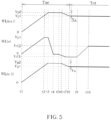
- FIG. 5 is a timing diagram of selected signals of the memory device 1 in FIG. 1 , employing the read method 400.
- the selected signals include signals on a word line WL(n) and adj acent word lines WL(n-1), WL(n+1).
- the word line WL(n) may be selected and the adjacent word lines WL(n-1), WL(n+1) may be unselected.
- the memory device 1 may perform a setup operation in a setup period Tset prior to a read operation in a read period Trd.
- the setup period Tset is between Times t1 and t8, in which the selected word line WL(n) and the unselected word lines WL(n-1), WL(n+1) are set up for the read operation.
- the row decoder 12 drives the selected word line WL(n) and the unselected word lines WL(n-1), WL(n+1) from a ground voltage (e.g., 0V) to the first pre-pulse voltage Vp1 (e.g., 4.5V). From Times t2 to t3, the row decoder 12 continues to drive the unselected word lines WL(n-1), WL(n+1) from the first pre-pulse voltage Vp1 to the second pre-pulse voltage Vp2 (e.g., 5.2V), while holding the selected word line WL(n) at the first pre-pulse voltage Vp1.
- a ground voltage e.g., 0V
- Vp1 e.g., 4.5V
- the second pre-pulse voltage Vp2 exceeds the first pre-pulse voltage Vp1 by a voltage difference Va, and Va may be less than 0.7V.
- the row decoder 12 grounds the selected word lines WL(n) from the first pre-pulse voltage Vp1 to the ground voltage, while holding the unselected word lines WL(n-1), WL(n+1) at the second pre-pulse voltage Vp2.
- the row decoder 12 maintains the selected word lines WL(n) at the ground voltage, and the unselected word lines WL(n-1), WL(n+1) at the second pre-pulse voltage Vp2.
- the row decoder 12 pulls the selected word lines WL(n) from the ground voltage towards the start read level Vr(1), while holding the unselected word lines WL(n-1), WL(n+1) at the second pre-pulse voltage Vp2. From Times t6 to t7, the row decoder 12 drives the unselected word lines WL(n-1), WL (n+1) from the second pre-pulse voltage Vp2 towards the first pre-pulse voltage Vp1. Between Times t6 and t7, the selected word lines WL(n) may be floating or driven by the row decoder 12.
- the selected word lines WL(n) will continue to be driven towards the start read level Vr(1) by the negative coupling voltage induced by the pull-down voltages on the unselected word lines WL(n-1), WL(n+1).
- the selected word lines WL(n) will continue to be driven towards the start read level Vr(1) by both the row decoder 12 and the induced negative coupling voltage, reducing time required for reaching the start read level Vr(1).
- the row decoder 12 continues to drive the unselected word lines WL(n-1), WL(n+1) until the first pre-pulse voltage Vp1 is reached, while maintaining the selected word lines WL(n) at the start read level Vr(1).
- the memory device 1 uses a reduced time to set the selected word line WL(n) to the start read level Vr(1) and the unselected word lines WL(n-1), WL(n+1) to the first pre-pulse voltage Vp1.
- the memory device 1 starts the read operation.
- the row decoder 12 From Times t8 to t9, upon the voltages on the unselected word lines WL(n-1), WL(n+1) reaching the first pre-pulse voltage Vp1, the row decoder 12 continues to maintain the unselected word lines WL(n-1), WL (n+1) at the first pre-pulse voltage Vp1, and continues to maintain the selected word line WL(n) at the start read level Vr(1). From Times t9 to t10, the row decoder 12 drives the selected word lines WL(n) from the start read level Vr(1) to the next read level Vr(2) . After Time t10, the row decoder 12 may continue to drive the selected word lines WL(n) from one read level to another until the state of one or more selected memory cells on the selected word line WL (n) can be determined.
- the read method 600 comprises Steps S602 to S608, employing signal coupling from an adjacent word line of a selected word lines WL(n) to reduce time required for setting up the selected word lines WL (n) prior to a read operation. Steps S602 to S606 are used to set up the selected word line WL(n) and the adjacent word line to appropriate voltage levels prior to the read operation. Step S608 is used to perform the read operation. Any reasonable step change or adjustment is within the scope of the disclosure.
- Step S602 The row decoder 12 applies a first pre-pulse voltage Vp1 to an nth word line WL(n) while applying a second pre-pulse voltage Vp2 to an adj acent word line adjacent to the nth word line WL(n);
- Step S604 The row decoder 12 grounds the nth word line WL (n) while maintaining the second pre-pulse voltage Vp2 on the adjacent word line;
- Step S606 The row decoder 12 floats the adjacent word line while pulling a voltage on the nth word line WL(n) towards a start read level;
- Step S608 In a read operation, the row decoder 12 pulls the voltage on the nth word line WL(n) from the start read level to a next read level while maintaining the voltage on the adjacent word line at the first pre-pulse voltage Vp1.
- Steps S602, S604, S608 are similar to Steps S402, S404, S410.
- Step S606 the adjacent word line is left floating, the voltage thereon is driven by a capacitive coupling effect induced by the voltage change on the selected word line WL(n), resulting in a voltage ramp on the adjacent word line that brings the voltage of the adjacent word line to the first pre-pulse voltage Vp1.
- the voltage ramp on the adjacent word line generates a coupling voltage on the selected word line WL(n) to speed up the voltage change on the selected word line WL (n) and decrease the time required for reaching the start read level.
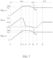
- FIG. 7 is a timing diagram of selected signals of the memory device in FIG. 1 , employing the read method 600.
- the selected signals include signals on a word line WL(n) and adj acent word lines WL(n-1), WL(n+1).
- the word line WL(n) may be selected and the adjacent word lines WL(n-1), WL(n+1) may be unselected.
- the memory device 1 may perform a setup operation in a setup period Tset prior to a read operation in a read period Trd.
- the setup period Tset is between Times t1 and t6, in which the selected word line WL(n) and the unselected word lines WL(n-1), WL(n+1) are set up for the read operation.
- the memory device 1 operates in a manner similar to FIG. 5 .
- the row decoder 12 drives the selected word line WL(n) from the ground voltage to the start read level Vr(1) and floats the unselected word lines WL(n-1), WL(n+1) .
- Cross coupling may occur between the unselected word lines WL(n-1), WL(n+1) and the selected word line WL(n), the voltage ramp-down on the selected word line WL (n) initiates voltage ramp-downs on the unselected word lines WL(n-1), WL(n+1), and the voltage ramp-downs on the unselected word lines WL(n-1), WL(n+1) further induce a steeper voltage ramp-down on the selected word line WL(n), reducing time taken for driving the selected word line WL(n) from the ground voltage to the start read level Vr(1).
- the row decoder 12 continues to maintain the unselected word lines WL(n-1), WL(n+1) at the first pre-pulse voltage Vp1, and upon the voltage on the selected word line WL (n) reaching the start read level Vr(1), the row decoder 12 continues to maintain the selected word line WL(n) at the start read level Vr(1).
- the memory device 1 uses a reduced time to set the selected word line WL(n) to the start read level Vr (1) and the unselected word lines WL(n-1), WL(n+1) to the first pre-pulse voltage Vp1.
- the row decoder 12 drives the selected word lines WL(n) from the start read level Vr(1) to the next read level Vr(2).
- the row decoder 12 may continue to drive the selected word lines WL(n) from one read level to another until the state of one or more selected memory cells on the selected word line WL(n) can be determined.
- the memory device 1 and the read methods 400, 600 employ a coupling effect from an adjacent word line of a selected word line to drive the selected word line to a start read level at an increased speed, setting the selected word line to the start read level using a reduced time, saving time required for setting up selected word line prior to a read operation.
Landscapes
- Engineering & Computer Science (AREA)
- Microelectronics & Electronic Packaging (AREA)
- Computer Hardware Design (AREA)
- Read Only Memory (AREA)
- Static Random-Access Memory (AREA)
Priority Applications (1)
| Application Number | Priority Date | Filing Date | Title |
|---|---|---|---|
| EP23178442.2A EP4235672B1 (de) | 2019-11-28 | 2019-11-28 | Verfahren zur erhöhung der geschwindigkeit des lesens von daten aus einer speichervorrichtung |
Applications Claiming Priority (3)
| Application Number | Priority Date | Filing Date | Title |
|---|---|---|---|
| PCT/CN2019/121510 WO2021102777A1 (en) | 2019-11-28 | 2019-11-28 | Methods of enhancing speed of reading data from memory device |
| EP23178442.2A EP4235672B1 (de) | 2019-11-28 | 2019-11-28 | Verfahren zur erhöhung der geschwindigkeit des lesens von daten aus einer speichervorrichtung |
| EP19953729.1A EP3915115B1 (de) | 2019-11-28 | 2019-11-28 | Verfahren zur erhöhung der geschwindigkeit des lesens von daten aus einer speichervorrichtung |
Related Parent Applications (2)
| Application Number | Title | Priority Date | Filing Date |
|---|---|---|---|
| EP19953729.1A Division EP3915115B1 (de) | 2019-11-28 | 2019-11-28 | Verfahren zur erhöhung der geschwindigkeit des lesens von daten aus einer speichervorrichtung |
| EP19953729.1A Division-Into EP3915115B1 (de) | 2019-11-28 | 2019-11-28 | Verfahren zur erhöhung der geschwindigkeit des lesens von daten aus einer speichervorrichtung |
Publications (3)
| Publication Number | Publication Date |
|---|---|
| EP4235672A2 true EP4235672A2 (de) | 2023-08-30 |
| EP4235672A3 EP4235672A3 (de) | 2023-10-18 |
| EP4235672B1 EP4235672B1 (de) | 2025-02-12 |
Family
ID=70400236
Family Applications (2)
| Application Number | Title | Priority Date | Filing Date |
|---|---|---|---|
| EP23178442.2A Active EP4235672B1 (de) | 2019-11-28 | 2019-11-28 | Verfahren zur erhöhung der geschwindigkeit des lesens von daten aus einer speichervorrichtung |
| EP19953729.1A Active EP3915115B1 (de) | 2019-11-28 | 2019-11-28 | Verfahren zur erhöhung der geschwindigkeit des lesens von daten aus einer speichervorrichtung |
Family Applications After (1)
| Application Number | Title | Priority Date | Filing Date |
|---|---|---|---|
| EP19953729.1A Active EP3915115B1 (de) | 2019-11-28 | 2019-11-28 | Verfahren zur erhöhung der geschwindigkeit des lesens von daten aus einer speichervorrichtung |
Country Status (7)
| Country | Link |
|---|---|
| US (2) | US11056196B2 (de) |
| EP (2) | EP4235672B1 (de) |
| JP (1) | JP7358496B2 (de) |
| KR (1) | KR102665095B1 (de) |
| CN (2) | CN112466374B (de) |
| TW (1) | TWI729668B (de) |
| WO (1) | WO2021102777A1 (de) |
Families Citing this family (8)
| Publication number | Priority date | Publication date | Assignee | Title |
|---|---|---|---|---|
| WO2021232223A1 (en) * | 2020-05-19 | 2021-11-25 | Yangtze Memory Technologies Co., Ltd. | 3d nand flash and operation method thereof |
| JP2022018404A (ja) * | 2020-07-15 | 2022-01-27 | キオクシア株式会社 | 半導体記憶装置 |
| US20220230674A1 (en) * | 2021-01-21 | 2022-07-21 | Macronix International Co., Ltd. | Read operation method for non-volatile memory device to reduce disturbance |
| CN113257304B (zh) * | 2021-06-22 | 2021-10-08 | 上海亿存芯半导体有限公司 | 存储器及数据存储和读取方法 |
| KR20250052449A (ko) * | 2022-12-30 | 2025-04-18 | 양쯔 메모리 테크놀로지스 씨오., 엘티디. | 메모리 디바이스와 그에 대한 읽기 작업 |
| KR20240109128A (ko) | 2023-01-03 | 2024-07-10 | 삼성전자주식회사 | 비휘발성 메모리 장치 및 그의 동작 방법 |
| US12249365B2 (en) * | 2023-03-06 | 2025-03-11 | Windbond Electronics Corp. | Memory device capable of performing in-memory computing |
| US12333150B1 (en) | 2023-12-13 | 2025-06-17 | Nxp B.V. | Partitioned non-volatile memory (NVM) having a normal read bus and a verify read bus |
Family Cites Families (38)
| Publication number | Priority date | Publication date | Assignee | Title |
|---|---|---|---|---|
| JP4157065B2 (ja) * | 2004-03-29 | 2008-09-24 | 株式会社東芝 | 半導体記憶装置 |
| US7064981B2 (en) * | 2004-08-04 | 2006-06-20 | Micron Technology, Inc. | NAND string wordline delay reduction |
| TWI380311B (en) * | 2006-12-29 | 2012-12-21 | Sandisk Technologies Inc | Systems and methods for margined neighbor reading for non-volatile memory read operations including coupling compensation |
| EP2122628B1 (de) * | 2007-02-07 | 2012-05-30 | MOSAID Technologies Incorporated | Quellenseitiges asymmetrisches vorlade-programmierungsschema |
| ITRM20070273A1 (it) * | 2007-05-16 | 2008-11-17 | Micron Technology Inc | Lettura di celle di memoria non volatile a livello mutiplo. |
| KR101416740B1 (ko) * | 2007-11-26 | 2014-07-09 | 삼성전자주식회사 | 플래시 메모리 장치 및 그것의 읽기 방법 |
| JP2010129125A (ja) | 2008-11-27 | 2010-06-10 | Toshiba Corp | 多値不揮発性半導体メモリ |
| JP2011170956A (ja) * | 2010-02-18 | 2011-09-01 | Samsung Electronics Co Ltd | 不揮発性メモリ装置およびそのプログラム方法と、それを含むメモリシステム |
| US8274831B2 (en) * | 2010-05-24 | 2012-09-25 | Sandisk Technologies Inc. | Programming non-volatile storage with synchronized coupling |
| JP2012027988A (ja) * | 2010-07-23 | 2012-02-09 | Toshiba Corp | 半導体記憶装置およびその制御方法 |
| JP5198529B2 (ja) * | 2010-09-22 | 2013-05-15 | 株式会社東芝 | 不揮発性半導体記憶装置 |
| JP5595901B2 (ja) * | 2010-12-28 | 2014-09-24 | 株式会社東芝 | 不揮発性半導体記憶装置 |
| US8472266B2 (en) | 2011-03-31 | 2013-06-25 | Sandisk Technologies Inc. | Reducing neighbor read disturb |
| JP5017480B1 (ja) * | 2011-05-02 | 2012-09-05 | 株式会社東芝 | 半導体記憶装置 |
| JP2013012267A (ja) * | 2011-06-29 | 2013-01-17 | Toshiba Corp | 不揮発性半導体記憶装置 |
| KR102127416B1 (ko) * | 2013-06-27 | 2020-06-26 | 삼성전자주식회사 | 비휘발성 메모리 장치, 그것을 포함하는 메모리 시스템 및 그것의 읽기 방법 |
| KR102058664B1 (ko) | 2013-08-29 | 2019-12-23 | 삼성전자주식회사 | 불휘발성 메모리 장치 및 그것의 동작 방법 |
| US9047970B2 (en) * | 2013-10-28 | 2015-06-02 | Sandisk Technologies Inc. | Word line coupling for deep program-verify, erase-verify and read |
| KR102233810B1 (ko) * | 2014-02-03 | 2021-03-30 | 삼성전자주식회사 | 비휘발성 메모리 장치 및 그것의 워드라인 구동 방법 |
| KR101556681B1 (ko) * | 2014-07-02 | 2015-10-02 | 서울대학교산학협력단 | 셀 스트링에서의 읽기 방법 |
| KR102273185B1 (ko) * | 2014-07-09 | 2021-07-06 | 삼성전자주식회사 | 비휘발성 메모리 장치, 그것을 포함하는 저장 장치 및 그것의 구동 방법 |
| KR102182804B1 (ko) * | 2014-07-29 | 2020-11-25 | 삼성전자주식회사 | 메모리 장치의 독출 방법 |
| KR20160024503A (ko) * | 2014-08-26 | 2016-03-07 | 삼성전자주식회사 | 반도체 메모리 장치 및 이를 포함하는 메모리 시스템 |
| JP6271460B2 (ja) | 2015-03-02 | 2018-01-31 | 東芝メモリ株式会社 | 半導体記憶装置 |
| KR20160110592A (ko) * | 2015-03-09 | 2016-09-22 | 에스케이하이닉스 주식회사 | 반도체 장치 및 이의 동작 방법 |
| KR102294352B1 (ko) * | 2015-04-20 | 2021-08-26 | 삼성전자주식회사 | 불휘발성 메모리 장치 및 그것의 프로그램 방법과 독출 방법 |
| KR20160136675A (ko) | 2015-05-20 | 2016-11-30 | 에스케이하이닉스 주식회사 | 반도체 메모리 장치 및 그것의 동작 방법 |
| KR102504294B1 (ko) * | 2016-03-25 | 2023-02-28 | 삼성전자 주식회사 | 메모리 장치, 메모리 시스템 및 이에 대한 독출/검증 동작 방법 |
| KR102499388B1 (ko) * | 2016-07-15 | 2023-02-14 | 에스케이하이닉스 주식회사 | 음의 전압 생성 장치를 포함하는 메모리 장치 |
| KR102633029B1 (ko) * | 2016-08-22 | 2024-02-06 | 삼성전자주식회사 | 불휘발성 메모리 장치, 불휘발성 메모리 장치를 포함하는 스토리지 장치 및 불휘발성 메모리 장치의 읽기 방법 |
| US9640273B1 (en) * | 2016-08-25 | 2017-05-02 | Sandisk Technologies Llc | Mitigating hot electron program disturb |
| KR102620820B1 (ko) * | 2016-09-23 | 2024-01-03 | 삼성전자주식회사 | 비휘발성 메모리 장치의 데이터 독출 방법 |
| CN108538333B (zh) * | 2017-03-06 | 2022-02-11 | 北京兆易创新科技股份有限公司 | Nand闪存的读操作处理方法、装置和nand存储设备 |
| JP2018156711A (ja) * | 2017-03-21 | 2018-10-04 | 東芝メモリ株式会社 | メモリコントローラおよびデータ読み出し方法 |
| CN108735265A (zh) * | 2017-04-24 | 2018-11-02 | 北京兆易创新科技股份有限公司 | 一种读操作方法和装置 |
| CN109215696B (zh) * | 2017-06-29 | 2022-10-04 | 爱思开海力士有限公司 | 执行编程操作的非易失性存储器件及其操作方法 |
| CN207302634U (zh) * | 2017-09-05 | 2018-05-01 | 珠海泓芯科技有限公司 | 存储器读取电路 |
| KR102288138B1 (ko) * | 2018-01-08 | 2021-08-10 | 삼성전자주식회사 | 메모리 장치 |
-
2019
- 2019-11-28 EP EP23178442.2A patent/EP4235672B1/de active Active
- 2019-11-28 CN CN202011441406.5A patent/CN112466374B/zh active Active
- 2019-11-28 KR KR1020217029203A patent/KR102665095B1/ko active Active
- 2019-11-28 JP JP2021554775A patent/JP7358496B2/ja active Active
- 2019-11-28 CN CN201980003405.1A patent/CN111095419B/zh active Active
- 2019-11-28 EP EP19953729.1A patent/EP3915115B1/de active Active
- 2019-11-28 WO PCT/CN2019/121510 patent/WO2021102777A1/en not_active Ceased
-
2020
- 2020-01-07 US US16/736,754 patent/US11056196B2/en active Active
- 2020-01-08 TW TW109100596A patent/TWI729668B/zh active
-
2021
- 2021-05-25 US US17/330,290 patent/US11468954B2/en active Active
Also Published As
| Publication number | Publication date |
|---|---|
| CN112466374B (zh) | 2023-01-13 |
| TW202121180A (zh) | 2021-06-01 |
| EP4235672B1 (de) | 2025-02-12 |
| CN112466374A (zh) | 2021-03-09 |
| EP3915115A1 (de) | 2021-12-01 |
| US11056196B2 (en) | 2021-07-06 |
| EP4235672A3 (de) | 2023-10-18 |
| US11468954B2 (en) | 2022-10-11 |
| EP3915115B1 (de) | 2023-07-19 |
| EP3915115A4 (de) | 2022-06-29 |
| WO2021102777A1 (en) | 2021-06-03 |
| US20210166769A1 (en) | 2021-06-03 |
| JP2022525116A (ja) | 2022-05-11 |
| KR102665095B1 (ko) | 2024-05-09 |
| CN111095419A (zh) | 2020-05-01 |
| TWI729668B (zh) | 2021-06-01 |
| CN111095419B (zh) | 2021-01-29 |
| US20210280258A1 (en) | 2021-09-09 |
| JP7358496B2 (ja) | 2023-10-10 |
| KR20210124452A (ko) | 2021-10-14 |
Similar Documents
| Publication | Publication Date | Title |
|---|---|---|
| EP3915115B1 (de) | Verfahren zur erhöhung der geschwindigkeit des lesens von daten aus einer speichervorrichtung | |
| US12080360B2 (en) | Reducing programming disturbance in memory devices | |
| KR100890016B1 (ko) | 비휘발성 메모리 장치, 그것을 포함하는 메모리 시스템 및그것의 프로그램 방법 | |
| US7668014B2 (en) | Non-volatile memory device and program method | |
| TWI628657B (zh) | Semiconductor memory device | |
| KR102655678B1 (ko) | 메모리 디바이스의 프로그램 교란을 감소시키는 방법 및 이를 이용한 메모리 디바이스 | |
| JP6492202B1 (ja) | 半導体記憶装置および消去方法 | |
| JP5992983B2 (ja) | 不揮発性半導体記憶装置 | |
| US20130294155A1 (en) | Plural operation of memory device | |
| US9196366B2 (en) | Semiconductor memory apparatus and method for erasing the same | |
| KR20160005840A (ko) | 반도체 장치 | |
| JP5631436B2 (ja) | 半導体記憶装置 | |
| US8824206B2 (en) | Non-volatile semiconductor memory device and readout method thereof | |
| JP5467938B2 (ja) | 半導体メモリ | |
| KR20160000034A (ko) | 반도체 장치 | |
| CN121153081A (zh) | 存储器装置、存储器系统及其操作方法 | |
| JP2010218623A (ja) | 不揮発性半導体記憶装置 | |
| CN104934063B (zh) | 半导体存储装置及擦除方法 | |
| CN121713241A (zh) | 存储器装置及其操作方法 |
Legal Events
| Date | Code | Title | Description |
|---|---|---|---|
| PUAI | Public reference made under article 153(3) epc to a published international application that has entered the european phase |
Free format text: ORIGINAL CODE: 0009012 |
|
| STAA | Information on the status of an ep patent application or granted ep patent |
Free format text: STATUS: REQUEST FOR EXAMINATION WAS MADE |
|
| 17P | Request for examination filed |
Effective date: 20230609 |
|
| AC | Divisional application: reference to earlier application |
Ref document number: 3915115 Country of ref document: EP Kind code of ref document: P |
|
| AK | Designated contracting states |
Kind code of ref document: A2 Designated state(s): AL AT BE BG CH CY CZ DE DK EE ES FI FR GB GR HR HU IE IS IT LI LT LU LV MC MK MT NL NO PL PT RO RS SE SI SK SM TR |
|
| PUAL | Search report despatched |
Free format text: ORIGINAL CODE: 0009013 |
|
| AK | Designated contracting states |
Kind code of ref document: A3 Designated state(s): AL AT BE BG CH CY CZ DE DK EE ES FI FR GB GR HR HU IE IS IT LI LT LU LV MC MK MT NL NO PL PT RO RS SE SI SK SM TR |
|
| RIC1 | Information provided on ipc code assigned before grant |
Ipc: G11C 16/34 20060101ALI20230912BHEP Ipc: G11C 16/32 20060101ALI20230912BHEP Ipc: G11C 16/26 20060101ALI20230912BHEP Ipc: G11C 16/10 20060101ALI20230912BHEP Ipc: G11C 16/08 20060101ALI20230912BHEP Ipc: G11C 16/04 20060101ALI20230912BHEP Ipc: G11C 11/56 20060101AFI20230912BHEP |
|
| STAA | Information on the status of an ep patent application or granted ep patent |
Free format text: STATUS: EXAMINATION IS IN PROGRESS |
|
| 17Q | First examination report despatched |
Effective date: 20240524 |
|
| GRAP | Despatch of communication of intention to grant a patent |
Free format text: ORIGINAL CODE: EPIDOSNIGR1 |
|
| STAA | Information on the status of an ep patent application or granted ep patent |
Free format text: STATUS: GRANT OF PATENT IS INTENDED |
|
| INTG | Intention to grant announced |
Effective date: 20241022 |
|
| P01 | Opt-out of the competence of the unified patent court (upc) registered |
Free format text: CASE NUMBER: APP_61760/2024 Effective date: 20241119 |
|
| GRAS | Grant fee paid |
Free format text: ORIGINAL CODE: EPIDOSNIGR3 |
|
| GRAA | (expected) grant |
Free format text: ORIGINAL CODE: 0009210 |
|
| STAA | Information on the status of an ep patent application or granted ep patent |
Free format text: STATUS: THE PATENT HAS BEEN GRANTED |
|
| AC | Divisional application: reference to earlier application |
Ref document number: 3915115 Country of ref document: EP Kind code of ref document: P |
|
| AK | Designated contracting states |
Kind code of ref document: B1 Designated state(s): AL AT BE BG CH CY CZ DE DK EE ES FI FR GB GR HR HU IE IS IT LI LT LU LV MC MK MT NL NO PL PT RO RS SE SI SK SM TR |
|
| REG | Reference to a national code |
Ref country code: GB Ref legal event code: FG4D |
|
| REG | Reference to a national code |
Ref country code: CH Ref legal event code: EP |
|
| REG | Reference to a national code |
Ref country code: DE Ref legal event code: R096 Ref document number: 602019066034 Country of ref document: DE |
|
| REG | Reference to a national code |
Ref country code: IE Ref legal event code: FG4D |
|
| REG | Reference to a national code |
Ref country code: NL Ref legal event code: MP Effective date: 20250212 |
|
| PG25 | Lapsed in a contracting state [announced via postgrant information from national office to epo] |
Ref country code: RS Free format text: LAPSE BECAUSE OF FAILURE TO SUBMIT A TRANSLATION OF THE DESCRIPTION OR TO PAY THE FEE WITHIN THE PRESCRIBED TIME-LIMIT Effective date: 20250512 |
|
| PG25 | Lapsed in a contracting state [announced via postgrant information from national office to epo] |
Ref country code: FI Free format text: LAPSE BECAUSE OF FAILURE TO SUBMIT A TRANSLATION OF THE DESCRIPTION OR TO PAY THE FEE WITHIN THE PRESCRIBED TIME-LIMIT Effective date: 20250212 |
|
| PG25 | Lapsed in a contracting state [announced via postgrant information from national office to epo] |
Ref country code: PL Free format text: LAPSE BECAUSE OF FAILURE TO SUBMIT A TRANSLATION OF THE DESCRIPTION OR TO PAY THE FEE WITHIN THE PRESCRIBED TIME-LIMIT Effective date: 20250212 |
|
| PG25 | Lapsed in a contracting state [announced via postgrant information from national office to epo] |
Ref country code: ES Free format text: LAPSE BECAUSE OF FAILURE TO SUBMIT A TRANSLATION OF THE DESCRIPTION OR TO PAY THE FEE WITHIN THE PRESCRIBED TIME-LIMIT Effective date: 20250212 |
|
| REG | Reference to a national code |
Ref country code: LT Ref legal event code: MG9D |
|
| PG25 | Lapsed in a contracting state [announced via postgrant information from national office to epo] |
Ref country code: IS Free format text: LAPSE BECAUSE OF FAILURE TO SUBMIT A TRANSLATION OF THE DESCRIPTION OR TO PAY THE FEE WITHIN THE PRESCRIBED TIME-LIMIT Effective date: 20250612 Ref country code: NO Free format text: LAPSE BECAUSE OF FAILURE TO SUBMIT A TRANSLATION OF THE DESCRIPTION OR TO PAY THE FEE WITHIN THE PRESCRIBED TIME-LIMIT Effective date: 20250512 |
|
| PG25 | Lapsed in a contracting state [announced via postgrant information from national office to epo] |
Ref country code: NL Free format text: LAPSE BECAUSE OF FAILURE TO SUBMIT A TRANSLATION OF THE DESCRIPTION OR TO PAY THE FEE WITHIN THE PRESCRIBED TIME-LIMIT Effective date: 20250212 |
|
| PG25 | Lapsed in a contracting state [announced via postgrant information from national office to epo] |
Ref country code: HR Free format text: LAPSE BECAUSE OF FAILURE TO SUBMIT A TRANSLATION OF THE DESCRIPTION OR TO PAY THE FEE WITHIN THE PRESCRIBED TIME-LIMIT Effective date: 20250212 |
|
| PG25 | Lapsed in a contracting state [announced via postgrant information from national office to epo] |
Ref country code: PT Free format text: LAPSE BECAUSE OF FAILURE TO SUBMIT A TRANSLATION OF THE DESCRIPTION OR TO PAY THE FEE WITHIN THE PRESCRIBED TIME-LIMIT Effective date: 20250612 Ref country code: LV Free format text: LAPSE BECAUSE OF FAILURE TO SUBMIT A TRANSLATION OF THE DESCRIPTION OR TO PAY THE FEE WITHIN THE PRESCRIBED TIME-LIMIT Effective date: 20250212 |
|
| PG25 | Lapsed in a contracting state [announced via postgrant information from national office to epo] |
Ref country code: GR Free format text: LAPSE BECAUSE OF FAILURE TO SUBMIT A TRANSLATION OF THE DESCRIPTION OR TO PAY THE FEE WITHIN THE PRESCRIBED TIME-LIMIT Effective date: 20250513 Ref country code: BG Free format text: LAPSE BECAUSE OF FAILURE TO SUBMIT A TRANSLATION OF THE DESCRIPTION OR TO PAY THE FEE WITHIN THE PRESCRIBED TIME-LIMIT Effective date: 20250212 |
|
| REG | Reference to a national code |
Ref country code: AT Ref legal event code: MK05 Ref document number: 1766879 Country of ref document: AT Kind code of ref document: T Effective date: 20250212 |
|
| PG25 | Lapsed in a contracting state [announced via postgrant information from national office to epo] |
Ref country code: SE Free format text: LAPSE BECAUSE OF FAILURE TO SUBMIT A TRANSLATION OF THE DESCRIPTION OR TO PAY THE FEE WITHIN THE PRESCRIBED TIME-LIMIT Effective date: 20250212 |
|
| PG25 | Lapsed in a contracting state [announced via postgrant information from national office to epo] |
Ref country code: SM Free format text: LAPSE BECAUSE OF FAILURE TO SUBMIT A TRANSLATION OF THE DESCRIPTION OR TO PAY THE FEE WITHIN THE PRESCRIBED TIME-LIMIT Effective date: 20250212 |
|
| PG25 | Lapsed in a contracting state [announced via postgrant information from national office to epo] |
Ref country code: DK Free format text: LAPSE BECAUSE OF FAILURE TO SUBMIT A TRANSLATION OF THE DESCRIPTION OR TO PAY THE FEE WITHIN THE PRESCRIBED TIME-LIMIT Effective date: 20250212 |
|
| PG25 | Lapsed in a contracting state [announced via postgrant information from national office to epo] |
Ref country code: IT Free format text: LAPSE BECAUSE OF FAILURE TO SUBMIT A TRANSLATION OF THE DESCRIPTION OR TO PAY THE FEE WITHIN THE PRESCRIBED TIME-LIMIT Effective date: 20250212 |
|
| PG25 | Lapsed in a contracting state [announced via postgrant information from national office to epo] |
Ref country code: AT Free format text: LAPSE BECAUSE OF FAILURE TO SUBMIT A TRANSLATION OF THE DESCRIPTION OR TO PAY THE FEE WITHIN THE PRESCRIBED TIME-LIMIT Effective date: 20250212 |
|
| PG25 | Lapsed in a contracting state [announced via postgrant information from national office to epo] |
Ref country code: EE Free format text: LAPSE BECAUSE OF FAILURE TO SUBMIT A TRANSLATION OF THE DESCRIPTION OR TO PAY THE FEE WITHIN THE PRESCRIBED TIME-LIMIT Effective date: 20250212 Ref country code: CZ Free format text: LAPSE BECAUSE OF FAILURE TO SUBMIT A TRANSLATION OF THE DESCRIPTION OR TO PAY THE FEE WITHIN THE PRESCRIBED TIME-LIMIT Effective date: 20250212 |
|
| PG25 | Lapsed in a contracting state [announced via postgrant information from national office to epo] |
Ref country code: RO Free format text: LAPSE BECAUSE OF FAILURE TO SUBMIT A TRANSLATION OF THE DESCRIPTION OR TO PAY THE FEE WITHIN THE PRESCRIBED TIME-LIMIT Effective date: 20250212 |
|
| PG25 | Lapsed in a contracting state [announced via postgrant information from national office to epo] |
Ref country code: SK Free format text: LAPSE BECAUSE OF FAILURE TO SUBMIT A TRANSLATION OF THE DESCRIPTION OR TO PAY THE FEE WITHIN THE PRESCRIBED TIME-LIMIT Effective date: 20250212 |
|
| REG | Reference to a national code |
Ref country code: DE Ref legal event code: R097 Ref document number: 602019066034 Country of ref document: DE |
|
| PLBE | No opposition filed within time limit |
Free format text: ORIGINAL CODE: 0009261 |
|
| STAA | Information on the status of an ep patent application or granted ep patent |
Free format text: STATUS: NO OPPOSITION FILED WITHIN TIME LIMIT |
|
| PGFP | Annual fee paid to national office [announced via postgrant information from national office to epo] |
Ref country code: DE Payment date: 20251118 Year of fee payment: 7 |
|
| PGFP | Annual fee paid to national office [announced via postgrant information from national office to epo] |
Ref country code: GB Payment date: 20251020 Year of fee payment: 7 |
|
| PGFP | Annual fee paid to national office [announced via postgrant information from national office to epo] |
Ref country code: FR Payment date: 20251020 Year of fee payment: 7 |
|
| 26N | No opposition filed |
Effective date: 20251113 |