JP5631436B2 - 半導体記憶装置 - Google Patents
半導体記憶装置 Download PDFInfo
- Publication number
- JP5631436B2 JP5631436B2 JP2013081020A JP2013081020A JP5631436B2 JP 5631436 B2 JP5631436 B2 JP 5631436B2 JP 2013081020 A JP2013081020 A JP 2013081020A JP 2013081020 A JP2013081020 A JP 2013081020A JP 5631436 B2 JP5631436 B2 JP 5631436B2
- Authority
- JP
- Japan
- Prior art keywords
- bit line
- voltage
- sense circuit
- soft program
- verify
- Prior art date
- Legal status (The legal status is an assumption and is not a legal conclusion. Google has not performed a legal analysis and makes no representation as to the accuracy of the status listed.)
- Active
Links
Images


Description
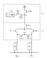
110:メモリアレイ
120:入出力バッファ
130:アドレスレジスタ
140:データレジスタ
150:コントローラ
160:ワード線選択回路
170:ページバッファ/センス回路
180:プリチャージ回路
190:列選択回路
200:内部電圧発生回路
GBL_e:偶数ビット線
GBL_o:奇数ビット線
SL:ソース線
VIR:仮想電位
SEL_e:偶数選択トランジスタ
SEL_o:奇数選択トランジスタ
BLS:ビット線選択トランジスタ
YSEL_e:偶数バイアストランジスタ
YSEL_o:奇数バイアストランジスタ
SSEL_e:偶数ソース線選択トランジスタ
SSEL_o:奇数ソース線選択トランジスタ
Claims (10)
- 複数のメモリセルが形成されたNAND型のメモリアレイと、
行方向のメモリセルを選択するワード線選択回路と、
メモリアレイの各ビット線に結合され、選択されたビット線を流れる電流が予め決められた値よりも大きいか否かを検出する電流検出型のセンス回路と、
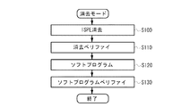
メモリアレイの選択されたブロックのメモリセルのデータを消去する消去手段とを含み、
前記消去手段は、消去ベリファイシーケンスと、ソフトプログラムシーケンスとを含み、
消去ベリファイシーケンスにおいて、消去されたブロックの全ワード線に第1のベリファイ電圧を印加したとき、前記センス回路により消去されたブロックの各ビット線に流れる電流が前記予め決められた値より大きいか否かを判定し、各ビット線を流れる電流が前記予め決められた値以上であれば消去を終了し、
前記ソフトプログラムシーケンスにおいて、消去されたブロックの全ワード線にソフトプログラム電圧を印加し、かつ全ワード線に前記第1のベリファイ電圧よりも大きい第2のベリファイ電圧を印加したとき、前記センス回路により消去されたブロックの各ビット線に流れる電流が前記予め決められた値より小さいか否かを判定するソフトプログラムベリファイを行い、各ビット線を流れる電流が前記予め決められた値よりも小さければソフトプログラムシーケンスを終了する、半導体記憶装置。 - 前記ソフトプログラムベリファイは、全ワード線に、読出し動作時に非選択ワード線に印加されるパス電圧を前記第2のベリファイ電圧として印加し、前記予め決められた値よりも小さいか否かを検知する、請求項1に記載の半導体記憶装置。
- 前記ソフトプログラムベリファイは、前記予め決められた値よりも小さいと検知されたビット線に書き込み禁止電圧を供給し、前記予め決められた値よりも大きいビット線に結合されたメモリセルにソフトプログラムを行う、請求項2に記載の半導体記憶装置。
- 半導体記憶装置はさらに、ビット線にプリチャージ電圧を供給する複数のプリチャージ回路を含み、複数のプリチャージ回路は、ブロック間に配置される、請求項1ないし3いずれか1つに記載の半導体記憶装置。
- 前記プリチャージ回路は、前記センス回路によりビット線に電流が供給される前にビット線にプリチャージ電圧を供給する、請求項4に記載の半導体記憶装置。
- 前記センス回路は、偶数ビット線に接続される第1のセンス回路と、奇数ビット線に接続される第2のセンス回路とを含み、第1のセンス回路は、メモリアレイの一方の端部に配置され、第2のセンス回路は、メモリアレイの他方の端部に配置され、第1のセンス回路と第2のセンス回路との間に、複数のプリチャージ回路が配置される、請求項4または5に記載の半導体記憶装置。
- 前記プリチャージ回路は、前記ワード線選択回路からメモリアレイの行方向に延在し、前記ビット線に接続される配線を含む、請求項4ないし6いずれか1つに記載の半導体記憶装置。
- NAND型の不揮発性メモリセルを備えた半導体記憶装置における消去方法であって、
消去されたブロックの全ワード線に第1のベリファイ電圧を印加したとき、各ビット線に流れる電流が、電流センス回路により予め決められた値より大きいか否かを判定し、各ビット線を流れる電流が前記予め決められた値以上であれば消去を終了する消去ベリファイシーケンスと、
消去されたブロックの全ワード線にソフトプログラム電圧を印加し、消去されたブロックの全ワード線に前記第1のベリファイ電圧よりも大きい第2のベリファイ電圧を印加したとき、各ビット線に流れる電流が前記予め決められた値より小さいか否かを判定し、各ビット線を流れる電流が前記予め決められた値よりも小さければソフトプログラムシーケンスを終了するソフトプログラムシーケンスと、
を有する消去方法。 - 前記ソフトプログラムシーケンスは、全ワード線に、読出し動作時に非選択ワード線に印加されるパス電圧を前記第2のベリファイ電圧として印加し、前記予め決められた値よりも小さいか否かを検知する、請求項8に記載の消去方法。
- 前記ソフトプログラムシーケンスは、前記予め決められた値よりも小さいと検知されたビット線に書き込み禁止電圧を供給し、前記予め決められた値よりも大きいビット線に結合されたメモリセルにソフトプログラムを行う、請求項8に記載の消去方法。
Priority Applications (1)
| Application Number | Priority Date | Filing Date | Title |
|---|---|---|---|
| JP2013081020A JP5631436B2 (ja) | 2013-04-09 | 2013-04-09 | 半導体記憶装置 |
Applications Claiming Priority (1)
| Application Number | Priority Date | Filing Date | Title |
|---|---|---|---|
| JP2013081020A JP5631436B2 (ja) | 2013-04-09 | 2013-04-09 | 半導体記憶装置 |
Publications (2)
| Publication Number | Publication Date |
|---|---|
| JP2014203498A JP2014203498A (ja) | 2014-10-27 |
| JP5631436B2 true JP5631436B2 (ja) | 2014-11-26 |
Family
ID=52145040
Family Applications (1)
| Application Number | Title | Priority Date | Filing Date |
|---|---|---|---|
| JP2013081020A Active JP5631436B2 (ja) | 2013-04-09 | 2013-04-09 | 半導体記憶装置 |
Country Status (1)
| Country | Link |
|---|---|
| JP (1) | JP5631436B2 (ja) |
Cited By (2)
| Publication number | Priority date | Publication date | Assignee | Title |
|---|---|---|---|---|
| US10141036B2 (en) | 2016-08-24 | 2018-11-27 | Winbond Electronics Corp. | Semiconductor memory device and reading method thereof |
| US11170828B2 (en) | 2019-06-17 | 2021-11-09 | Winbond Electronics Corp. | Voltage generating circuit, semiconductor storage device and bit line charging method thereof |
Families Citing this family (2)
| Publication number | Priority date | Publication date | Assignee | Title |
|---|---|---|---|---|
| JP6887044B1 (ja) * | 2020-05-22 | 2021-06-16 | ウィンボンド エレクトロニクス コーポレーション | 半導体記憶装置および読出し方法 |
| JP6895002B1 (ja) * | 2020-05-27 | 2021-06-30 | ウィンボンド エレクトロニクス コーポレーション | 半導体記憶装置および読出し方法 |
Citations (6)
| Publication number | Priority date | Publication date | Assignee | Title |
|---|---|---|---|---|
| US3014A (en) * | 1843-03-21 | Improvement sn awl-hafts | ||
| JP2006523911A (ja) * | 2003-04-14 | 2006-10-19 | サンディスク コーポレイション | 低電圧の不揮発性メモリに適した読み出しと消去を検証する方法および回路 |
| JP2007172775A (ja) * | 2005-12-26 | 2007-07-05 | Toshiba Corp | センスアンプ及び半導体記憶装置 |
| JP2007305204A (ja) * | 2006-05-10 | 2007-11-22 | Toshiba Corp | 不揮発性半導体記憶装置 |
| JP2009230818A (ja) * | 2008-03-24 | 2009-10-08 | Toshiba Corp | 半導体記憶装置 |
| WO2011119500A1 (en) * | 2010-03-25 | 2011-09-29 | Sandisk Il Ltd. | Simultaneous multi-state read or verify in non-volatile storage |
-
2013
- 2013-04-09 JP JP2013081020A patent/JP5631436B2/ja active Active
Patent Citations (6)
| Publication number | Priority date | Publication date | Assignee | Title |
|---|---|---|---|---|
| US3014A (en) * | 1843-03-21 | Improvement sn awl-hafts | ||
| JP2006523911A (ja) * | 2003-04-14 | 2006-10-19 | サンディスク コーポレイション | 低電圧の不揮発性メモリに適した読み出しと消去を検証する方法および回路 |
| JP2007172775A (ja) * | 2005-12-26 | 2007-07-05 | Toshiba Corp | センスアンプ及び半導体記憶装置 |
| JP2007305204A (ja) * | 2006-05-10 | 2007-11-22 | Toshiba Corp | 不揮発性半導体記憶装置 |
| JP2009230818A (ja) * | 2008-03-24 | 2009-10-08 | Toshiba Corp | 半導体記憶装置 |
| WO2011119500A1 (en) * | 2010-03-25 | 2011-09-29 | Sandisk Il Ltd. | Simultaneous multi-state read or verify in non-volatile storage |
Cited By (3)
| Publication number | Priority date | Publication date | Assignee | Title |
|---|---|---|---|---|
| US10141036B2 (en) | 2016-08-24 | 2018-11-27 | Winbond Electronics Corp. | Semiconductor memory device and reading method thereof |
| US11170828B2 (en) | 2019-06-17 | 2021-11-09 | Winbond Electronics Corp. | Voltage generating circuit, semiconductor storage device and bit line charging method thereof |
| TWI750655B (zh) * | 2019-06-17 | 2021-12-21 | 華邦電子股份有限公司 | 電壓生成電路、半導體儲存裝置及其位元線充電方法 |
Also Published As
| Publication number | Publication date |
|---|---|
| JP2014203498A (ja) | 2014-10-27 |
Similar Documents
| Publication | Publication Date | Title |
|---|---|---|
| US6026025A (en) | Electrically erasable and programmable non-volatile semiconductor memory with automatic write-verify controller | |
| KR101119371B1 (ko) | 반도체 메모리 장치 및 이의 동작 방법 | |
| US10418113B2 (en) | Operation method for suppressing floating gate (FG) coupling | |
| JP5964401B2 (ja) | 不揮発性半導体記憶装置 | |
| US8923055B2 (en) | Semiconductor device and method of operating the same | |
| JP2008135100A (ja) | 半導体記憶装置及びそのデータ消去方法 | |
| JP5992983B2 (ja) | 不揮発性半導体記憶装置 | |
| JP5565948B2 (ja) | 半導体メモリ | |
| US20110194354A1 (en) | Non-volatile semiconductor memory device | |
| KR20090055806A (ko) | 불휘발성 메모리 소자의 프로그램 검증 방법 | |
| US9196366B2 (en) | Semiconductor memory apparatus and method for erasing the same | |
| US9865358B2 (en) | Flash memory device and erase method thereof capable of reducing power consumption | |
| JP2016100030A (ja) | 不揮発性半導体記憶装置 | |
| CN104347117A (zh) | 半导体存储装置及其擦除方法 | |
| KR950003348B1 (ko) | 자동 기입-검증 제어기를 갖는 전기적으로 소거가능하고 프로그램가능한 불휘발성 반도체 메모리 | |
| JP5631436B2 (ja) | 半導体記憶装置 | |
| JP5805162B2 (ja) | 半導体記憶装置 | |
| JP6154879B2 (ja) | Nand型フラッシュメモリとそのプログラム方法 | |
| JP4846814B2 (ja) | 不揮発性半導体記憶装置 | |
| US7782676B2 (en) | Method of operating a nonvolatile memory device | |
| JP6439026B1 (ja) | 半導体記憶装置 | |
| JP2000149577A (ja) | 不揮発性半導体記憶装置およびそのデータ書き込み方法 | |
| JP2010218623A (ja) | 不揮発性半導体記憶装置 | |
| KR101610176B1 (ko) | 반도체 메모리 장치 및 그것을 소거하는 방법 | |
| TWI514391B (zh) | 半導體記憶裝置及其抹除方法 |
Legal Events
| Date | Code | Title | Description |
|---|---|---|---|
| TRDD | Decision of grant or rejection written | ||
| A01 | Written decision to grant a patent or to grant a registration (utility model) |
Free format text: JAPANESE INTERMEDIATE CODE: A01 Effective date: 20141007 |
|
| A61 | First payment of annual fees (during grant procedure) |
Free format text: JAPANESE INTERMEDIATE CODE: A61 Effective date: 20141007 |
|
| R150 | Certificate of patent or registration of utility model |
Ref document number: 5631436 Country of ref document: JP Free format text: JAPANESE INTERMEDIATE CODE: R150 |
|
| R250 | Receipt of annual fees |
Free format text: JAPANESE INTERMEDIATE CODE: R250 |
|
| R250 | Receipt of annual fees |
Free format text: JAPANESE INTERMEDIATE CODE: R250 |
|
| R250 | Receipt of annual fees |
Free format text: JAPANESE INTERMEDIATE CODE: R250 |
|
| R250 | Receipt of annual fees |
Free format text: JAPANESE INTERMEDIATE CODE: R250 |
|
| R250 | Receipt of annual fees |
Free format text: JAPANESE INTERMEDIATE CODE: R250 |
|
| R250 | Receipt of annual fees |
Free format text: JAPANESE INTERMEDIATE CODE: R250 |
|
| R250 | Receipt of annual fees |
Free format text: JAPANESE INTERMEDIATE CODE: R250 |