JP5631436B2 - Semiconductor memory device - Google Patents
Semiconductor memory device Download PDFInfo
- Publication number
- JP5631436B2 JP5631436B2 JP2013081020A JP2013081020A JP5631436B2 JP 5631436 B2 JP5631436 B2 JP 5631436B2 JP 2013081020 A JP2013081020 A JP 2013081020A JP 2013081020 A JP2013081020 A JP 2013081020A JP 5631436 B2 JP5631436 B2 JP 5631436B2
- Authority
- JP
- Japan
- Prior art keywords
- bit line
- voltage
- sense circuit
- soft program
- verify
- Prior art date
- Legal status (The legal status is an assumption and is not a legal conclusion. Google has not performed a legal analysis and makes no representation as to the accuracy of the status listed.)
- Active
Links
Images


Landscapes
- Read Only Memory (AREA)
Description
本発明は、半導体記憶装置に関し、特に、NAND型フラッシュメモリの電流センシングを用いたデータの読出しに関する。 The present invention relates to a semiconductor memory device, and more particularly to reading data using current sensing of a NAND flash memory.
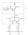
図1は、従来のフラッシュメモリのビット線選択回路およびページバッファ/センス回路の一例を示す図であり、ここには、一対のビット線として、偶数ビット線GBL_eと奇数ビット線GBL_oが例示されている。ビット線選択回路10は、偶数ビット線GBL_eに接続された偶数選択トランジスタSEL_eと、奇数ビット線GBL_oに接続された奇数選択トランジスタSEL_oと、偶数ビット線GBL_eと仮想電位VIRとの間に接続された偶数バイアス選択トランジスタYSEL_eと、奇数ビット線GBL_oと仮想電位VIRとの間に接続された奇数バイアス選択トランジスタYSEL_oと、偶数選択トランジスタSEL_eおよび奇数選択トランジスタSEL_oの共通ノードN1に接続されたビット線選択トランジスタBLSとを有する。
FIG. 1 is a diagram illustrating an example of a bit line selection circuit and a page buffer / sense circuit of a conventional flash memory, in which an even bit line GBL_e and an odd bit line GBL_o are illustrated as a pair of bit lines. Yes. The bit
偶数ビット線GBL_eおよび奇数ビット線GBL_oには、それぞれNANDストリングNUが接続される。NANDストリングNUは、直列に接続された複数のメモリセルとその両端に接続されたドレイン選択トランジスタおよびソース選択トランジスタとを含み、ドレイン選択トランジスタは偶数ビット線GBL_e/奇数ビット線GBL_oに接続され、ソース選択トランジスタは、共通のソース線SLに接続される。 A NAND string NU is connected to each of the even bit line GBL_e and the odd bit line GBL_o. The NAND string NU includes a plurality of memory cells connected in series and a drain selection transistor and a source selection transistor connected to both ends of the memory cell. The drain selection transistor is connected to the even bit line GBL_e / odd bit line GBL_o, The selection transistors are connected to a common source line SL.
センス回路20は、ビット線にプリチャージ電位を供給するためのプリチャージトランジスタBLPREと、プリチャージトランジスタBLPREとビット線選択トランジスタBLSとの間に形成されるセンスノードSNに接続されたキャパシタCと、センスノードSNの電位をラッチ回路12へ転送する転送トランジスタBLCD等を有する。
The
偶数ビット線GBL_eが選択されるとき、奇数ビット線GBL_oが非選択とされ、偶数選択トランジスタSEL_e、ビット線選択トランジスタBLSがオンし、奇数選択トランジスタSEL_oがオフする。また、奇数ビット線GBL_oが選択されるとき、偶数ビット線GBL_eが非選択とされ、奇数選択トランジスタSEL_o、ビット線選択トランジスタBLSがオンし、偶数選択トランジスタSEL_eがオフする。こうして、1つのセンス回路10は、2本のビット線GBL_eおよびGBL_oに共通に使用される。
When the even bit line GBL_e is selected, the odd bit line GBL_o is not selected, the even selection transistor SEL_e and the bit line selection transistor BLS are turned on, and the odd selection transistor SEL_o is turned off. When the odd bit line GBL_o is selected, the even bit line GBL_e is not selected, the odd selection transistor SEL_o and the bit line selection transistor BLS are turned on, and the even selection transistor SEL_e is turned off. Thus, one
読出し動作において、偶数ビット線GBL_eが選択され、奇数ビット線GBL_oが非選択されるとき、偶数バイアストランジスタYSEL_eがオフし、奇数バイアストランジスタYSEL_oがオンし、奇数ビット線GBL_oには仮想電位VIRによりGND電位が供給される。反対に、偶数ビット線GBL_eが非選択され、奇数ビット線GBL_oが選択されるとき、偶数バイアストランジスタYSEL_eがオンし、奇数バイアストランジスタYSEL_oがオフし、偶数ビット線GBL_eには仮想電位VIRによりGND電位が供給される。このように、偶数ビット線の読出しを行うとき、奇数ビット線にGND電位を供給し、奇数ビット線の読出しを行うとき、偶数ビット線にGND電位を供給することで、隣接するビット線間の容量結合によるノイズを低減するビット線シールドが特許文献1等に開示されている。
In the read operation, when the even bit line GBL_e is selected and the odd bit line GBL_o is not selected, the even bias transistor YSEL_e is turned off, the odd bias transistor YSEL_o is turned on, and the odd bit line GBL_o is grounded by the virtual potential VIR. A potential is supplied. Conversely, when the even bit line GBL_e is not selected and the odd bit line GBL_o is selected, the even bias transistor YSEL_e is turned on, the odd bias transistor YSEL_o is turned off, and the even bit line GBL_e is connected to the GND potential by the virtual potential VIR. Is supplied. As described above, when the even bit line is read, the GND potential is supplied to the odd bit line, and when the odd bit line is read, the GND potential is supplied to the even bit line. A bit line shield that reduces noise due to capacitive coupling is disclosed in
図1に示すセンス回路20は、いわゆる電圧検出型のセンス回路であり、偶数ビット線GBL_eまたは奇数ビット線GBL_oにプリチャージトランジスタBLPREを介してプリチャージ電位を供給し、その後、選択されたメモリセルの記憶状態に応じてビット線を放電させ、その放電状態をセンスノードSNで検出する。しかしながら、電圧検出型のセンス回路は、ビット線の微細化によりビット線抵抗が高くなり、また、NANDストリングを構成するメモリセル数の増加によりビット線容量も増加すると、時定数が大きくなり、ビット線の充放電に要する時間が長くなり、データの読出しに時間がかかってしまう。このため、電圧検出型のセンス回路は、もはや高集積化のフラッシュメモリには適さないものになりつつある。
A
このような理由から、センス回路には、電流検出型が用いられつつある。電流検出型のセンス回路は、メモリセルの記憶状態に応じてメモリセルを流れる電流をビット線を介して検出するものであり、電圧検出型と比較して高速センスが可能である。電流検出型のセンス回路は、例えば、電流−電圧変換を行うカスコード回路等が利用されている。 For this reason, a current detection type is being used for the sense circuit. The current detection type sensing circuit detects a current flowing through the memory cell through a bit line in accordance with the storage state of the memory cell, and can perform high-speed sensing compared to the voltage detection type. As the current detection type sensing circuit, for example, a cascode circuit that performs current-voltage conversion is used.
次に、従来の電流検出型のセンス回路の課題について説明する。フラッシュメモリにおいて、プログラムでは、フローティングゲートに電子を蓄積させ、メモリセルのしきい値電圧を正方向にシフトさせ、消去では、フローティングゲートから電子を放出させ、メモリセルのしきい値電圧を負方向にシフトさせるが、このようなプログラムおよび消去は、メモリセルのしきい値が「0」、「1」の分布幅内に入るように制御されなければならない。また、メモリセルに多ビットを記憶させる場合には、さらに「00」、「01」、「10」、「11」の分布幅に入るように制御しなければならない。メモリセルのしきい値をより正確に制御するため、従来より、ISPE(Incremental Step Pulse Erase)方式が用いられている。ISPEでは、選択されたブロックのメモリセルに初期の消去パルスVers0を印加し、消去ベリファイにより消去が不合格と判定された場合には、消去パルスVers0よりも1ステップ電圧だけ高い消去パルスVers1を印加し、ブロック内のすべてのメモリセルの消去が合格と判定されるまで消去パルスの電圧が順次増加されていく。 Next, problems of the conventional current detection type sensing circuit will be described. In flash memory, in programming, electrons are accumulated in the floating gate, and the threshold voltage of the memory cell is shifted in the positive direction. In erasing, electrons are discharged from the floating gate, and the threshold voltage of the memory cell is negatively changed. However, such programming and erasing must be controlled so that the threshold value of the memory cell falls within the distribution width of “0” and “1”. In addition, when multiple bits are stored in the memory cell, control must be performed so that the distribution widths of “00”, “01”, “10”, and “11” are included. Conventionally, an ISPE (Incremental Step Pulse Erase) method is used to control the threshold value of the memory cell more accurately. In ISPE, the initial erase pulse Vers0 is applied to the memory cell of the selected block. If the erase verify determines that the erase has failed, the erase pulse Vers1 that is one step voltage higher than the erase pulse Vers0 is applied. Then, the erase pulse voltage is sequentially increased until it is determined that the erase of all the memory cells in the block is acceptable.
ここで問題となるのは、各メモリセルのサイズや形状には、製造工程のパラメータの変動によってバラツキがあり、さらにプログラムや消去の回数等によりトンネル酸化膜が劣化するなどの要因があり、その結果、メモリセル間でデータが消去しやすいものと、そうでないものが生じる。つまり、あるメモリセルでは、コンダクタンスが大きいために電流が流れ易く、あるメモリセルでは、コンダクタンスが小さいために電流が流れ難いものが存在する。消去ベリファイでは、1つ1つのメモリセルの消去状態をチェックしておらず、ビット線単位でブロック全体の合否を判定している。このため、仮に、1つのビット線に、コンダクタンスの大きなメモリセルとコンダクタンスの小さなメモリセルが含まれていれば、コンダクタンスの小さなメモリセルを基準に合否の判定が成されることになり、コンダクタンスの大きなメモリセルは過消去(オーバーイレース)される。その結果、データの読出しにおいて、オーバーイレースされたメモリセルには相対的に大きな電流が流れ、電力消費が大きくなってしまう。同時に、センス回路側も大きな電流を供給する仕様にしなければならず、センス回路の小型化等の妨げとなる。 The problem here is that there are variations in the size and shape of each memory cell due to fluctuations in the parameters of the manufacturing process, and there are other factors such as deterioration of the tunnel oxide film due to the number of programming and erasing, etc. As a result, some data is easily erased between memory cells, and some data is not. That is, in some memory cells, the conductance is large and current flows easily, and in some memory cells, the conductance is small and current does not easily flow. In the erase verify, the erase state of each memory cell is not checked, and pass / fail of the entire block is determined in units of bit lines. For this reason, if a single bit line includes a memory cell having a large conductance and a memory cell having a small conductance, the pass / fail judgment is made based on the memory cell having a small conductance. Large memory cells are over-erased (over-erased). As a result, in reading data, a relatively large current flows through the overerased memory cells, and power consumption increases. At the same time, the sense circuit must be designed to supply a large current, which hinders downsizing the sense circuit.
本発明は、上記従来の課題を解決し、消費電力を抑制し高速動作が可能な半導体記憶装置を提供することを目的とする。 An object of the present invention is to solve the above-described conventional problems and to provide a semiconductor memory device that can operate at high speed while suppressing power consumption.
本発明に係る半導体記憶装置は、複数のメモリセルが形成されたメモリアレイと、行方向のメモリセルを選択するワード線選択回路と、メモリアレイの各ビット線に結合され、選択されたビット線を流れる電流を検出する電流検出型のセンス回路と、メモリアレイの選択されたブロックのメモリセルのデータを消去する消去手段とを含み、前記消去手段は、消去ベリファイシーケンスと、ソフトプログラムシーケンスとを含み、消去ベリファイシーケンスは、消去されたブロックの各ビット線に流れる電流が第1の値より大きいか否かを判定し、各ビット線を流れる電流が第1の値以上であれば消去を終了し、前記ソフトプログラムシーケンスは、消去されたブロックの全ワード線にソフトプログラム電圧を印加し、各ビット線に流れる電流が前記第1の値よりも小さい第2の値よりも小さいか否かを判定するソフトプログラムベリファイを行い、各ビット線を流れる電流が前記第2の値よりも小さければソフトプログラムシーケンスを終了する。 A semiconductor memory device according to the present invention includes a memory array in which a plurality of memory cells are formed, a word line selection circuit for selecting memory cells in the row direction, and a selected bit line coupled to each bit line of the memory array. Current detection type sensing circuit for detecting the current flowing through the memory array, and erasing means for erasing data in the memory cells of the selected block of the memory array, the erasing means comprising an erase verify sequence and a soft program sequence. In addition, the erase verify sequence determines whether or not the current flowing through each bit line of the erased block is greater than the first value, and if the current flowing through each bit line is equal to or greater than the first value, the erase is terminated. In the soft program sequence, a soft program voltage is applied to all the word lines of the erased block, and a current flowing through each bit line is Perform determining soft program verify whether the smaller smaller second value than the first value, the current flowing through each bit line is completed the soft program sequence is smaller than the second value.
好ましくは前記ソフトプログラムベリファイは、全ワード線に、読出し動作時に非選択ワード線に印加されるパス電圧を印加し、前記第2の値よりも小さいか否かを検知する。好ましくは前記ソフトプログラムベリファイは、前記第2の値よりも小さいと検知されたビット線に書き込み禁止電圧を供給し、前記第2の値よりも大きいビット線に結合されたメモリセルにソフトプログラムを行う。好ましくは半導体記憶装置はさらに、ビット線にプリチャージ電圧を供給する複数のプリチャージ回路を含み、複数のプリチャージ回路は、ブロック間に配置される。好ましくは前記プリチャージ回路は、前記センス回路によりビット線に電流が供給される前にビット線にプリチャージ電圧を供給する。好ましくは前記センス回路は、偶数ビット線に接続される第1のセンス回路と、奇数ビット線に接続される第2のセンス回路とを含み、第1のセンス回路は、メモリアレイの一方の端部に配置され、第2のセンス回路は、メモリアレイの他方の端部に配置され、第1のセンス回路と第2のセンス回路との間に、複数のプリチャージ回路が配置される。好ましくは前記プリチャージ回路は、前記ワード線選択回路からメモリアレイの行方向に延在し、前記ビット線に接続される配線を含む。 Preferably, the soft program verify applies a pass voltage applied to the unselected word lines during a read operation to all the word lines, and detects whether or not it is smaller than the second value. Preferably, the soft program verify supplies a write inhibit voltage to a bit line detected as being smaller than the second value, and performs a soft program on a memory cell coupled to the bit line larger than the second value. Do. Preferably, the semiconductor memory device further includes a plurality of precharge circuits for supplying a precharge voltage to the bit lines, and the plurality of precharge circuits are arranged between the blocks. Preferably, the precharge circuit supplies a precharge voltage to the bit line before a current is supplied to the bit line by the sense circuit. Preferably, the sense circuit includes a first sense circuit connected to the even-numbered bit line and a second sense circuit connected to the odd-numbered bit line, and the first sense circuit is connected to one end of the memory array. The second sense circuit is arranged at the other end of the memory array, and a plurality of precharge circuits are arranged between the first sense circuit and the second sense circuit. Preferably, the precharge circuit includes a wiring extending from the word line selection circuit in a row direction of the memory array and connected to the bit line.
本発明に係るNAND型の不揮発性メモリセルを備えた半導体記憶装置における消去方法は、消去されたブロックの各ビット線に流れる電流が第1の値より大きいか否かを判定し、各ビット線を流れる電流が第1の値以上であれば消去を終了する消去ベリファイシーケンスと、消去されたブロックの全ワード線にソフトプログラム電圧を印加し、各ビット線に流れる電流が前記第1の値よりも小さい第2の値より小さいか否かを判定し、各ビット線を流れる電流が前記第2の値よりも小さければソフトプログラムシーケンスを終了するソフトプログラムシーケンスとを有する。 An erasing method in a semiconductor memory device having a NAND type nonvolatile memory cell according to the present invention determines whether or not a current flowing through each bit line of an erased block is larger than a first value, and each bit line If the current flowing through the first block is equal to or higher than the first value, an erase verify sequence for ending the erase operation, and a soft program voltage is applied to all the word lines of the erased block. And a soft program sequence for ending the soft program sequence if the current flowing through each bit line is smaller than the second value.
本発明によれば、消費電力を抑制し高速動作が可能な電流検出型のセンス回路を用いた半導体記憶装置を提供することができる。 According to the present invention, it is possible to provide a semiconductor memory device using a current detection type sense circuit that can operate at high speed while suppressing power consumption.
本発明のフラッシュメモリでは、電流検出型のセンス回路を用いメモリセルを流れる電流の有無を判定する。読出し時の電流消費を抑制するため、メモリセルのデータの消去が行われるとき、メモリセルの負のしきい値が一定以上になることを抑制するためのスキームが実施される。これにより、読出し時に電流検出型のセンス回路からビット線へ供給される電流量が一定以下に抑制され、消費電力が低減される。以下、本発明の実施の形態について図面を参照して詳細に説明する。なお、図面は、分かり易くするために各部を強調して示してあり、実際のデバイスのスケールとは異なることに留意すべきである。 In the flash memory of the present invention, the presence or absence of a current flowing through the memory cell is determined using a current detection type sense circuit. In order to suppress current consumption at the time of reading, a scheme for suppressing the negative threshold value of the memory cell from exceeding a certain level when data in the memory cell is erased is implemented. As a result, the amount of current supplied from the current detection type sensing circuit to the bit line at the time of reading is suppressed below a certain level, and power consumption is reduced. Hereinafter, embodiments of the present invention will be described in detail with reference to the drawings. It should be noted that in the drawings, each part is highlighted for easy understanding, and is different from an actual device scale.
図2は、本発明の実施例に係るフラッシュメモリの構成を示すブロック図である。但し、ここに示すフラッシュメモリの構成は、例示であって、本発明は、必ずしもこのような構成に限定されるものではない。 FIG. 2 is a block diagram showing the configuration of the flash memory according to the embodiment of the present invention. However, the configuration of the flash memory shown here is an example, and the present invention is not necessarily limited to such a configuration.
本実施例のフラッシュメモリ100は、行列状に配列された複数のメモリセルを有するメモリアレイ110と、外部入出力端子I/Oに接続され入出力データを保持する入出力バッファ120と、入出力バッファ120からのアドレスデータを受け取るアドレスレジスタ130と、入出力されるデータを保持するデータレジスタ140、入出力バッファ120からのコマンドデータおよび外部制御信号(図示されないチップイネーブルやアドレスラッチイネーブル等)に基づき各部を制御する制御信号C1、C2、C3等を供給するコントローラ150と、アドレスレジスタ130からの行アドレス情報Axをデコードしデコード結果に基づきブロックの選択およびワード線の選択等を行うワード線選択回路160と、ワード線選択回路160によって選択されたページから読み出されたデータを保持したり、選択されたページへの書込みデータを保持するページバッファ/センス回路170と、ビット線にプリチャージ電圧を供給するプリチャージ回路180と、アドレスレジスタ130からの列アドレス情報Ayをデコードし当該デコード結果に基づきページバッファ170内の列データを選択する列選択回路190と、データの読出し、プログラムおよび消去等のために必要な電圧(プログラム電圧Vpgm、パス電圧Vpass、読出しパス電圧Vread、消去電圧Vers、ソフトプログラム電圧Vsoft、非選択読出し電圧VPASSR)などを生成する内部電圧発生回路200とを含んで構成される。
The flash memory 100 according to this embodiment includes a
メモリアレイ110は、列方向に配置された複数のブロックBLK(0)、BLK(1)、・・・、BLK(m)を有する。ブロックの両側には、ページバッファ/センス回路170が配置され、メモリアレイ110の列方向には、複数のプリチャージ回路180が配置される。
The
図3は、メモリブロック内に形成されるNANDストリングの構成とブロック間に配置されるプリチャージ回路を示す図である。1つのメモリブロックには、複数のメモリセルを直列に接続したNANDストリングNUが複数形成され、図3には、1つのメモリブロック内にn+1個のセルユニットNUが行方向に配列されている。 FIG. 3 is a diagram showing a configuration of a NAND string formed in a memory block and a precharge circuit arranged between the blocks. In one memory block, a plurality of NAND strings NU in which a plurality of memory cells are connected in series are formed. In FIG. 3, n + 1 cell units NU are arranged in the row direction in one memory block.
セルユニットNUは、直列に接続された複数のメモリセルMCi(i=0、1、・・・、31)と、一方の端部であるメモリセルMC31のドレイン側に接続された選択トランジスタTR1と、他方の端部であるメモリセルMC0のソース側に接続された選択トランジスタTR2とを含み、選択トランジスタTR1のドレインは、対応する1つのビット線GBLに接続され、選択トランジスタTR2のソースは、共通のソース線SLに接続される。 The cell unit NU includes a plurality of memory cells MCi (i = 0, 1,..., 31) connected in series, and a selection transistor TR1 connected to the drain side of the memory cell MC31 which is one end. , The selection transistor TR2 connected to the source side of the memory cell MC0 which is the other end, the drain of the selection transistor TR1 is connected to one corresponding bit line GBL, and the source of the selection transistor TR2 is common Connected to the source line SL.
メモリセルMCiのコントロールゲートは、ワード線WLiに接続され、選択トランジスタTR1、TR2のゲートは、ワード線WLと並行する選択ゲート線SGD、SGSに接続される。ワード線選択回路160は、行アドレスAxに基づきメモリブロックを選択するとき、当該メモリブロックの選択ゲート信号SGS、SGDを介して選択トランジスタTR1、TR2を選択的に駆動する。
The control gate of the memory cell MCi is connected to the word line WLi, and the gates of the selection transistors TR1 and TR2 are connected to selection gate lines SGD and SGS parallel to the word line WL. When selecting a memory block based on the row address Ax, the word
典型的に、半導体基板または半導体層内にPウエルが形成され、1つのPウエル内に1つのブロックが形成される。メモリセルは、N型の拡散領域であるソース/ドレインと、ソース/ドレイン間のチャンネル上に形成されたトンネル酸化膜と、トンネル酸化膜上に形成された電荷と蓄積するフローティングゲート(電荷蓄積層)と、フローティングゲート上に誘電体膜を介して形成されたコントロールゲートとを含むMOS構造を有する。フローティングゲートに電荷が蓄積されていないときまたは消去されたとき、つまりデータ「1」が保持されているとき、しきい値は負状態にあり、メモリセルは、ノーマリオンである。フローティングゲートに電子が蓄積されたときまたはプログラムされたとき、つまりデータ「0」が保持されているとき、しきい値は正にシフトし、メモリセルは、ノーマリオフである。 Typically, a P well is formed in a semiconductor substrate or semiconductor layer, and one block is formed in one P well. The memory cell includes a source / drain that is an N-type diffusion region, a tunnel oxide film formed on a channel between the source / drain, and a floating gate (charge storage layer) that accumulates charges formed on the tunnel oxide film. ) And a control gate formed on the floating gate via a dielectric film. When charge is not accumulated in the floating gate or when it is erased, that is, when data “1” is held, the threshold value is in a negative state, and the memory cell is normally on. When electrons are stored or programmed in the floating gate, that is, when data “0” is held, the threshold value shifts to positive, and the memory cell is normally off.
また、図3に示すように、ブロックBLK(i)とブロックBLK(i+1)との間には、ビット線GBLにプリチャージ電圧を供給するためのプリチャージ回路180が挿入される。プリチャージ回路180が挿入される位置および数は任意であるが、好ましくは、プリチャージ回路180とページバッファ/センス回路170との間に含まれるブロックの数や、プリチャージ回路180の間に含まれるブロックの数が等しいか近似されるように、プリチャージ回路が配置される。プリチャージ回路180を設けることにより、ビット線をプリチャージする時間を短縮する。
Further, as shown in FIG. 3, a
好ましい例では、プリチャージ回路180は、偶数ビット線GBL_eに接続される偶数プリチャージトランジスタPRE_eと、奇数ビット線GBL_oに接続される奇数プリチャージトランジスタPRE_oとを含む。偶数プリチャージトランジスタPRE_eおよび奇数プリチャージトランジスタPRE_oは、ワード線選択回路160内に形成され、コントローラ150からの制御信号に基づき動作される。偶数プリチャージトランジスタPRE_eおよび奇数プリチャージトランジスタPRE_oにそれぞれ接続された金属配線WP_e、WP_oがメモリアレイ110上を行方向に延び、金属配線WP_eが偶数ビット線GBL_eに接続され、金属配線WP_oが奇数ビット線GBL_eに接続される。好ましくは、金属配線WP_e、WP_oは、ソース線SL上を延在する。例えば、読み出し動作が行われるとき、偶数プリチャージトランジスタPRE_eまたは奇数プリチャージトランジスタPRE_oがオンされ、偶数ビット線GBL_eまたは奇数ビット線GBL_oにプリチャージ電位Vpreが供給される。
In a preferred example, the
セルユニットNUに接続されたビット線GBL0、GBL1、・・・、GBLnは、ビット線選択回路を介してページバッファ/センス回路170に接続される。ビット線選択回路は、読出し時やプログラム時等に、偶数ビット線または奇数ビット線を選択し、選択された偶数ビット線または奇数ビット線をページバッファ/センス回路170に接続する。例えば、偶数ビット線が選択されるとき、偶数ビット線は、メモリアレイ110の上方のページバッファ/センス回路170に接続され、奇数ビット線が選択されたとき、奇数ビット線は、メモリアレイ110の下方のページバッファ/センス回路170に接続される。
Bit lines GBL0, GBL1,..., GBLn connected to the cell unit NU are connected to the page buffer /
図4は、本実施例のページバッファ/センス回路の一例を示す回路図である。ここでは、1つの偶数ビット線GBL_eに接続されたページバッファ/センス回路170を例にする。ページバッファ/センス回路170は、読出し時に、偶数ビット線GBL_eの電流を検出するためのセンス回路と、読み出されたデータやプログラムするデータを保持するラッチ回路等を含む。
FIG. 4 is a circuit diagram showing an example of the page buffer / sense circuit of this embodiment. Here, the page buffer /
本実施例のセンス回路は、電流検出型であり、電流検出型のセンス回路は、公知の回路によって構成することができる。図4は、簡略化されたカスコード回路を例示するが、これ以外にも、リファレンス用のカスコード回路を用意し、2つのカスコード回路によって電流−電圧変換された信号を差動増幅回路によって増幅するような回路であってもよい。図4に示すセンス回路は、Vdd電源に接続されたPチャンネルMOSトランジスタM1と、PMOSトランジスタM1に直列に接続された抵抗Rと、抵抗Rに直列に接続されたNチャンネルMOSトランジスタM2と、NMOSトランジスタM2のゲートに接続されたCMOSインバータINとを含んで構成される。 The sense circuit of this embodiment is a current detection type, and the current detection type sense circuit can be configured by a known circuit. FIG. 4 illustrates a simplified cascode circuit. In addition to this, a cascode circuit for reference is prepared, and a signal that has been subjected to current-voltage conversion by two cascode circuits is amplified by a differential amplifier circuit. It may be a simple circuit. The sense circuit shown in FIG. 4 includes a P-channel MOS transistor M1 connected to the Vdd power source, a resistor R connected in series to the PMOS transistor M1, an N-channel MOS transistor M2 connected in series to the resistor R, and an NMOS. And a CMOS inverter IN connected to the gate of the transistor M2.
トランジスタM1のゲートには、センス回路を活性化させるための/信号Activeが入力され、このトランジスタM1は、電流源として機能する。トランジスタM2のゲートにはインバータINの出力が結合され、インバータINは、ビット線GBL_eの反転した電位をトランジスタM2に印加する。つまり、ノードN2は、ビット線選択回路を介して偶数ビット線GBL_eに接続され、偶数ビット線GBL_eを流れる電流を監視する。ビット線GBL_eのメモリセルに電流が流れると、ノードN2が低下しトランジスタM2がオンし、トランジスタM1を流れる検出電流が抵抗Rによって電圧に変換され、センスノードSNから検出電流に応じた電圧(抵抗R×当該抵抗Rを流れる検出電流)が出力される。選択されたビット線GBL_eに電流が流れないとき、あるいは微小な電流が流れるとき、トランジスタM2はオフし、検出電流が抵抗Rを流れないためセンスノードSNの出力Outはゼロである。なお、偶数ビット線の読出しが行われるとき、奇数ビット線を基準電位にし、反対に、奇数ビット線の読出しが行われるとき、偶数ビット線を基準電位にするシールド読出しが行われるようにしてもよい。本実施例の電流検出型のセンス回路は、後述するように供給する最大の電流値を一定以下に制限するように動作され、読出しやベリファイ時等の電力消費を抑制する。 The / signal Active for activating the sense circuit is input to the gate of the transistor M1, and the transistor M1 functions as a current source. The output of the inverter IN is coupled to the gate of the transistor M2, and the inverter IN applies the inverted potential of the bit line GBL_e to the transistor M2. That is, the node N2 is connected to the even bit line GBL_e via the bit line selection circuit, and monitors the current flowing through the even bit line GBL_e. When a current flows through the memory cell of the bit line GBL_e, the node N2 is lowered and the transistor M2 is turned on, and the detected current flowing through the transistor M1 is converted into a voltage by the resistor R. R × detection current flowing through the resistor R) is output. When no current flows through the selected bit line GBL_e or when a very small current flows, the transistor M2 is turned off, and the detection current does not flow through the resistor R, so the output Out of the sense node SN is zero. When the even bit line is read, the odd bit line is set to the reference potential, and conversely, when the odd bit line is read, the shield read is performed using the even bit line as the reference potential. Good. The current detection type sense circuit of this embodiment is operated so as to limit the maximum current value to be supplied to a certain value or less as will be described later, and suppresses power consumption during reading and verification.
次に、本実施例に係るフラッシュメモリの動作について説明する。図5の表は、消去、書込み、読出し動作時に印加される電圧のバイアス条件の一例を示している。Fは、フローティングである。コントローラ150は、読出し、プログラムまたは消去に関するコマンドを受け取ると、当該コマンドを解読し、ワード線駆動回路160、列選択回路190、内部電圧発生回路200等を制御し、各動作を実行させる。
Next, the operation of the flash memory according to this embodiment will be described. The table of FIG. 5 shows an example of bias conditions for the voltages applied during erase, write, and read operations. F is floating. When the
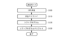
本実施例によるフラッシュメモリでは、図6に示すようなシーケンスを含む消去モードが実行される。コントローラ150は、消去に関するコマンドを受け取ると、図6に示す消去モードを実行する。この消去モードは、選択されたブロックに消去パルスを印加してメモリセルのデータを消去するISPE消去(S100)と、メモリセルのしきい値電圧が消去ベリファイ電圧以下になっていることを確認するための消去ベリファイ(S110)と、メモリセルのしきい値分布幅を狭くするようなソフトプログラム(S120)、およびソフトプログラムベリファイ(S130)とを含む。
In the flash memory according to the present embodiment, an erase mode including a sequence as shown in FIG. 6 is executed. When the
図7は、消去ベリファイ(ERV)およびソフトプログラム(SPGM)のときに印加される信号波形のタイミングチャートである。フラッシュメモリの消去では、公知にように選択されたブロック内のメモリセルのデータが一括で消去される。例えば、コントローラ150の制御により、選択されたブロックの全ワード線には0Vが印加され、選択ゲート信号SGD、SGSがフローティングにされ、Pウエルに約20Vの消去電圧Versが印加され、メモリセルのデータの一括消去が行われる。
FIG. 7 is a timing chart of signal waveforms applied during erase verify (ERV) and soft program (SPGM). In erasing the flash memory, the data in the memory cells in the block selected as is well known is erased at once. For example, under the control of the
次に、コントローラ150の制御の下で、消去ベリファイが実行される。消去ベリファイ(ERV)では、図7に示すように、選択されたブロック内の全ワード線に0Vが印加され、選択ゲート信号SGD、SGSに電源電圧Vddが印加され、センス回路によって全ビット線に電圧(例えば、0.8V)が印加される。消去ベリファイが行われる際、ビット線には、プリチャージ回路180からプリチャージ電圧Vpreが供給され、ビット線がセンス回路170に接続されたとき、ビット線の電圧が変化させないようにする。すなわち、センス回路170がビット線に接続される時点より前の一定期間、図3に示す偶数プリチャージトランジスタPRE_eまたは奇数プリチャージトランジスタPRE_oがオンされる。センス回路170へのビット線の接続に際して、ビット線の電圧変動を最小にするため、プリチャージ電圧Vpreとセンス回路170が供給する電圧とは等しいことが望ましい。
Next, erase verify is executed under the control of the
選択されたブロック内のメモリセルの電荷が消去されたとき、しきい値電圧は負の方向にシフトされ、メモリセルはデータ「1」の状態になる。但し、メモリセルのトンネル酸化膜の劣化やその他要因によりメモリセル間にはバラツキがあるため、メモリセル間のしきい値電圧にもバラツキが生じる。消去ベリファイは、選択されたブロック内のメモリセルのしきい値電圧がベリファイのしきい値電圧Vth以下になったか否かを確認する。本実施例では、センス回路170は電流検出型であるため、全ビット線の各々を流れる電流がしきい値電流以上、例えば1μA以上であるとき、消去が合格であると判定される。図4に示すセンス回路において、しきい値電流以上がトランジスタM1を流れるとき、センスノードSNには当該しきい値電流に応じた比較的高い電圧が表れる。もし、ビット線に含まれるメモリセルが電流を流さないとき、あるいはメモリセルを流れる電流がしきい値電流未満であるとき、センスノードSNにはゼロまたは比較的小さい電圧が表れる。センスノードSNから出力される電圧に基づき、消去が合格か不合格かが確認される。もし、消去が不合格であることが確認されると、前回印加された消去パルスよりも一定電圧だけ大きな消去パルスがPウエルに印加され、メモリセルのしきい値電圧がさらに負の方向へシフトされる。このような消去−消去ベリファイを繰り返すことで、消去ベリファイの合格が確認された時点で、ブロック内のメモリセルのしきい値電圧の分布幅の上限値Vmaxは、ベリファイのしきい値電流に相当するしきい値電圧Vth以下であることが保証される。図8(A)は、消去ベリファイが終了した時点のメモリセルのしきい値分布を表しており、しきい値電圧の分布幅の上限値Vmaxは、消去ベリファイのしきい値電流に相当するしきい値電圧Vthよりも小さい。メモリセルを流れる電流は、しきい値電圧Vthを確定させるドレイン電流Idである。
When the charge of the memory cell in the selected block is erased, the threshold voltage is shifted in the negative direction, and the memory cell enters the data “1” state. However, since the memory cells vary due to deterioration of the tunnel oxide film of the memory cells and other factors, the threshold voltage between the memory cells also varies. In the erase verify, it is confirmed whether or not the threshold voltage of the memory cell in the selected block is equal to or lower than the verify threshold voltage Vth. In this embodiment, since the
次に、メモリセルのしきい値電圧の分布幅が狭くなるようなソフトプログラム/ベリファイが行われる。データ消去/消去ベリファイでは、分布幅の上限値Vmaxをしきい値Vthよりも小さくするが、分布幅の下限値Vminについては考慮されていない。ISPE消去/消去ベリファイでは、最も電流を流しにくいメモリセルを対象にブロック全体に消去パルスを印加するため、ブロック内には、過消去状態のメモリセル、すなわちしきい値電圧が大きく負の方向にシフトされたメモリセルが存在する。そこで、ソフトプログラムでは、ブロック内のワード線に、通常のプログラムのときに印加する電圧Vpgmよりも小さいソフトプログラム電圧Vsoft1を印加することで、メモリセルに電荷を注入させ、しきい値電圧を正の方向へシフトさせるようなストレスを与える。 Next, soft programming / verification is performed so that the threshold voltage distribution width of the memory cell is narrowed. In the data erasure / erase verification, the upper limit value Vmax of the distribution width is made smaller than the threshold value Vth, but the lower limit value Vmin of the distribution width is not taken into consideration. In ISPE erase / erase verify, an erase pulse is applied to the entire block for the memory cell that is most difficult to pass current. Therefore, in the block, an over-erased memory cell, that is, the threshold voltage is large and in the negative direction. There are shifted memory cells. Therefore, in the soft program, by applying a soft program voltage Vsoft1 smaller than the voltage Vpgm applied in the normal program to the word lines in the block, charges are injected into the memory cell, and the threshold voltage is positive. Applying stress that shifts in the direction of
図9は、本実施例のソフトプログラム/ベリファイの動作フローを示す図である。ソフトプログラムでは、メモリ等に予め設定された初期ソフトプログラム電圧Vsoft1が設定され(S200)、図7に示すように、選択されたブロック内の全ワード線に、ソフトプログラム電圧Vsoft1が印加され、選択ゲート信号SGD、SGSに電源電圧Vddが印加され、全ビット線にプログラム可能な電圧0Vが印加される(S202)。この際、プリチャージ回路180は、消去ベリファイのときと同様に、ビット線にプリチャージ電圧Vpreを供給する。ソフトプログラム電圧Vsoft1は、通常のプログラム電圧Vpgmよりも小さく、相対的にオーバーイレース状態のメモリセルに電荷が注入され易く、上限値近傍のメモリセルには電荷が注入され難い。従って、図8(B)に示すように、分布幅の下限値近傍のメモリセルのしきい値電圧が正の方向へシフトされ、結果的に、分布幅が狭帯化される。
FIG. 9 is a diagram showing an operation flow of the soft program / verify according to the present embodiment. In the soft program, an initial soft program voltage Vsoft1 preset in a memory or the like is set (S200), and the soft program voltage Vsoft1 is applied to all the word lines in the selected block as shown in FIG. A power supply voltage Vdd is applied to the gate signals SGD and SGS, and a programmable voltage 0 V is applied to all bit lines (S202). At this time, the
ソフトプログラムベリファイでは、選択されたブロック内の全ワード線に、非選択ワード線へのパス電圧VPASSR(図5のテーブルの例では、4.5V)が印加される(S204)。このベリファイでも、消去ベリファイのときと同様に、プリチャージ回路180による充電が行われ、かつ選択ゲート信号SGD、SGSにも同様のバイアス電圧が印加される。次に、センス回路170において、ビット線を流れる電流がしきい値電流未満(Id<1μA)であるか否かが検出され、しきい値電流未満であれば、ソフトプログラムが合格であることを確認する(S206)。つまり、図4のセンスノードSNの出力に比較的小さな電圧が出力されたときに合格を確認する。ソフトプログラムが不合格であること確認した場合には、次のソフトプログラムが実施される(S208)。この場合、前回のソフトプログラム電圧Vsoft1よりも大きなソフトプログラム電圧Vsoft2が、不合格とされたページに印加される。また、既にソフトプログラムの合格を確認されたビット線には、例えば昇圧回路等によって昇圧されたプログラム禁止の電圧が供給される。これにより、不合格とされたビット線のメモリセルのしきい値がさらに正の方向へシフトされる。このようなソフトプログラムおよびベリファイが、すべてのビット線で合格するまで繰り返される(S210)。最終的に、ソフトプログラムを終了したブロックの各ビット線を流れる電流は、1μA近傍に収束されることになる。なお、図8(C)は、プログラムベリファイのしきい値分布であり、例えば、選択されたワード線に1.5Vが印加されたとき、ビット線に流れる電流は、Id<0.15μAである。
In the soft program verify, the pass voltage VPASSR (4.5 V in the example of the table of FIG. 5) to the unselected word line is applied to all the word lines in the selected block (S204). In this verify, as in the erase verify, charging by the
本実施例によれば、しきい値電圧の分布幅の下限値を正の方向シフトさせ、メモリセルのしきい値電圧の分布幅狭くしたので、データの読出し時にセンス回路からビット線を介して供給される電流の上限を制限することができ、これにより、電力消費を抑制することができる。すなわち、ソフトプログラムベリファイでは、全ワード線に、読出し時の非選択ワード線へのパス電圧VPASSRを印加し、しきい値電流よりも小さな電流を流すビット線を検知し、それを合格させるようにしたので、読出し時にセンス回路が供給する最大電流を抑制することができる。このことは、同時にセンス回路の小型化にも繋がる。さらにセンス回路からセルユニットNUを接続するビット線間の任意の複数の地点に、プリチャージ電圧を供給するようにしたので、センス回路からビット線を充電する時間を大幅に短縮させることができ、読出しやプログラムの高速化を図ることができる。 According to the present embodiment, since the lower limit value of the threshold voltage distribution width is shifted in the positive direction and the threshold voltage distribution width of the memory cell is narrowed, the data is read from the sense circuit via the bit line. The upper limit of the supplied current can be limited, and thereby power consumption can be suppressed. That is, in the soft program verify, the pass voltage VPASSR to the unselected word line at the time of reading is applied to all the word lines, and the bit line that flows a current smaller than the threshold current is detected and passed. Therefore, the maximum current supplied by the sense circuit during reading can be suppressed. This also leads to downsizing of the sense circuit. Furthermore, since the precharge voltage is supplied to any plurality of points between the bit lines connecting the cell units NU from the sense circuit, the time for charging the bit lines from the sense circuit can be greatly reduced. Reading and programming can be speeded up.
上記実施例では、メモリアレイの上下に一対のページバッファ/センス回路を配置し、それぞれのページバッファ/センス回路が偶数ビット線と奇数ビット線に接続される例を示したが、1つのページバッファ/センス回路が偶数ビット線および奇数ビット線に共有されるものであってもよい。この場合、ページバッファ/センス回路170は、図10に示すようにビット線選択回路10を介して偶数ビット線GBL_eおよび奇数ビット線GBL_eに選択的に接続される。さらに本実施例のように一対のページバッファ/センス回路をそれぞれ偶数ビット線および奇数ビット線に接続させた場合、奇数ビット線の読出しを行うとき、偶数ビット線をGND等の基準電位にし、他方、偶数ビット線の読出しを行うとき、奇数ビット線をGND等の基準電位にするビット線シールドを行うようにしてもよい。
In the above embodiment, a pair of page buffers / sense circuits are arranged above and below the memory array, and each page buffer / sense circuit is connected to an even bit line and an odd bit line. / The sense circuit may be shared by even bit lines and odd bit lines. In this case, the page buffer /
上記実施例では、消去モードが図6に示すようなシーケンスを包含する例を示したが、消去ベリファイモードが図6に示すようなシーケンスを包含するものであってもよい。上記実施例では、メモリセルは2値データを保持する例を示したが、メモリセルは多値データを保持するものであってもよい。さらに上記実施例で示した数値は、単なる例示であることは言うまでもない。 In the above embodiment, the erase mode includes the sequence as shown in FIG. 6, but the erase verify mode may include the sequence as shown in FIG. In the above embodiment, an example is shown in which the memory cell holds binary data, but the memory cell may hold multilevel data. Furthermore, it goes without saying that the numerical values shown in the above embodiments are merely examples.
本発明の好ましい実施の形態について詳述したが、本発明は、特定の実施形態に限定されるものではなく、特許請求の範囲に記載された本発明の要旨の範囲内において、種々の変形・変更が可能である。 Although the preferred embodiments of the present invention have been described in detail, the present invention is not limited to the specific embodiments, and various modifications and changes can be made within the scope of the gist of the present invention described in the claims. It can be changed.
100:フラッシュメモリ
110:メモリアレイ
120:入出力バッファ
130:アドレスレジスタ
140:データレジスタ
150:コントローラ
160:ワード線選択回路
170:ページバッファ/センス回路
180:プリチャージ回路
190:列選択回路
200:内部電圧発生回路
GBL_e:偶数ビット線
GBL_o:奇数ビット線
SL:ソース線
VIR:仮想電位
SEL_e:偶数選択トランジスタ
SEL_o:奇数選択トランジスタ
BLS:ビット線選択トランジスタ
YSEL_e:偶数バイアストランジスタ
YSEL_o:奇数バイアストランジスタ
SSEL_e:偶数ソース線選択トランジスタ
SSEL_o:奇数ソース線選択トランジスタ
100: flash memory 110: memory array 120: input / output buffer 130: address register 140: data register 150: controller 160: word line selection circuit 170: page buffer / sense circuit 180: precharge circuit 190: column selection circuit 200: internal Voltage generation circuit
GBL_e: Even bit line
GBL_o: Odd bit line
SL: Source line
VIR: Virtual potential
SEL_e: Even selection transistor
SEL_o: Odd select transistor
BLS: Bit line selection transistor
YSEL_e: Even bias transistor
YSEL_o: Odd bias transistor
SSEL_e: Even source line selection transistor
SSEL_o: Odd source line selection transistor
Claims (10)
行方向のメモリセルを選択するワード線選択回路と、
メモリアレイの各ビット線に結合され、選択されたビット線を流れる電流が予め決められた値よりも大きいか否かを検出する電流検出型のセンス回路と、
メモリアレイの選択されたブロックのメモリセルのデータを消去する消去手段とを含み、
前記消去手段は、消去ベリファイシーケンスと、ソフトプログラムシーケンスとを含み、
消去ベリファイシーケンスにおいて、消去されたブロックの全ワード線に第1のベリファイ電圧を印加したとき、前記センス回路により消去されたブロックの各ビット線に流れる電流が前記予め決められた値より大きいか否かを判定し、各ビット線を流れる電流が前記予め決められた値以上であれば消去を終了し、
前記ソフトプログラムシーケンスにおいて、消去されたブロックの全ワード線にソフトプログラム電圧を印加し、かつ全ワード線に前記第1のベリファイ電圧よりも大きい第2のベリファイ電圧を印加したとき、前記センス回路により消去されたブロックの各ビット線に流れる電流が前記予め決められた値より小さいか否かを判定するソフトプログラムベリファイを行い、各ビット線を流れる電流が前記予め決められた値よりも小さければソフトプログラムシーケンスを終了する、半導体記憶装置。 A NAND type memory array in which a plurality of memory cells are formed;
A word line selection circuit for selecting memory cells in the row direction;
A current detection type sensing circuit that is coupled to each bit line of the memory array and detects whether a current flowing through the selected bit line is greater than a predetermined value ;
Erasing means for erasing data in memory cells of a selected block of the memory array,
The erase means includes an erase verify sequence and a soft program sequence,
Whether or not the current flowing through each bit line of the block erased by the sense circuit is greater than the predetermined value when a first verify voltage is applied to all word lines of the erased block in the erase verify sequence If the current flowing through each bit line is equal to or greater than the predetermined value, erasing is terminated,
In the soft program sequence , when a soft program voltage is applied to all word lines of an erased block and a second verify voltage larger than the first verify voltage is applied to all word lines, the sense circuit current flowing to each bit line of the erased block performs the determining soft program verify whether the smaller than a predetermined value, is smaller than the value current is the predetermined flowing through each bit line soft A semiconductor memory device that ends a program sequence.
消去されたブロックの全ワード線に第1のベリファイ電圧を印加したとき、各ビット線に流れる電流が、電流センス回路により予め決められた値より大きいか否かを判定し、各ビット線を流れる電流が前記予め決められた値以上であれば消去を終了する消去ベリファイシーケンスと、
消去されたブロックの全ワード線にソフトプログラム電圧を印加し、消去されたブロックの全ワード線に前記第1のベリファイ電圧よりも大きい第2のベリファイ電圧を印加したとき、各ビット線に流れる電流が前記予め決められた値より小さいか否かを判定し、各ビット線を流れる電流が前記予め決められた値よりも小さければソフトプログラムシーケンスを終了するソフトプログラムシーケンスと、
を有する消去方法。 An erasing method in a semiconductor memory device including a NAND type nonvolatile memory cell,
When the first verify voltage is applied to all the word lines of the erased block, it is determined whether or not the current flowing through each bit line is greater than a value predetermined by the current sense circuit , and flows through each bit line. An erase verify sequence for ending erase if the current is equal to or greater than the predetermined value;
When a soft program voltage is applied to all the word lines of the erased block and a second verify voltage higher than the first verify voltage is applied to all the word lines of the erased block , the current flowing through each bit line a soft program sequence but determines whether the less than a predetermined value, the current flowing through each bit line is to terminate if smaller soft program sequence than said predetermined value,
An erasing method comprising:
Priority Applications (1)
| Application Number | Priority Date | Filing Date | Title |
|---|---|---|---|
| JP2013081020A JP5631436B2 (en) | 2013-04-09 | 2013-04-09 | Semiconductor memory device |
Applications Claiming Priority (1)
| Application Number | Priority Date | Filing Date | Title |
|---|---|---|---|
| JP2013081020A JP5631436B2 (en) | 2013-04-09 | 2013-04-09 | Semiconductor memory device |
Publications (2)
| Publication Number | Publication Date |
|---|---|
| JP2014203498A JP2014203498A (en) | 2014-10-27 |
| JP5631436B2 true JP5631436B2 (en) | 2014-11-26 |
Family
ID=52145040
Family Applications (1)
| Application Number | Title | Priority Date | Filing Date |
|---|---|---|---|
| JP2013081020A Active JP5631436B2 (en) | 2013-04-09 | 2013-04-09 | Semiconductor memory device |
Country Status (1)
| Country | Link |
|---|---|
| JP (1) | JP5631436B2 (en) |
Cited By (2)
| Publication number | Priority date | Publication date | Assignee | Title |
|---|---|---|---|---|
| US10141036B2 (en) | 2016-08-24 | 2018-11-27 | Winbond Electronics Corp. | Semiconductor memory device and reading method thereof |
| US11170828B2 (en) | 2019-06-17 | 2021-11-09 | Winbond Electronics Corp. | Voltage generating circuit, semiconductor storage device and bit line charging method thereof |
Families Citing this family (2)
| Publication number | Priority date | Publication date | Assignee | Title |
|---|---|---|---|---|
| JP6887044B1 (en) * | 2020-05-22 | 2021-06-16 | ウィンボンド エレクトロニクス コーポレーション | Semiconductor storage device and readout method |
| JP6895002B1 (en) * | 2020-05-27 | 2021-06-30 | ウィンボンド エレクトロニクス コーポレーション | Semiconductor storage device and readout method |
Citations (6)
| Publication number | Priority date | Publication date | Assignee | Title |
|---|---|---|---|---|
| US3014A (en) * | 1843-03-21 | Improvement sn awl-hafts | ||
| JP2006523911A (en) * | 2003-04-14 | 2006-10-19 | サンディスク コーポレイション | Method and circuit for verifying read and erase suitable for low voltage non-volatile memory |
| JP2007172775A (en) * | 2005-12-26 | 2007-07-05 | Toshiba Corp | Sense amplifier and semiconductor memory device |
| JP2007305204A (en) * | 2006-05-10 | 2007-11-22 | Toshiba Corp | Nonvolatile semiconductor memory device |
| JP2009230818A (en) * | 2008-03-24 | 2009-10-08 | Toshiba Corp | Semiconductor storage device |
| WO2011119500A1 (en) * | 2010-03-25 | 2011-09-29 | Sandisk Il Ltd. | Simultaneous multi-state read or verify in non-volatile storage |
-
2013
- 2013-04-09 JP JP2013081020A patent/JP5631436B2/en active Active
Patent Citations (6)
| Publication number | Priority date | Publication date | Assignee | Title |
|---|---|---|---|---|
| US3014A (en) * | 1843-03-21 | Improvement sn awl-hafts | ||
| JP2006523911A (en) * | 2003-04-14 | 2006-10-19 | サンディスク コーポレイション | Method and circuit for verifying read and erase suitable for low voltage non-volatile memory |
| JP2007172775A (en) * | 2005-12-26 | 2007-07-05 | Toshiba Corp | Sense amplifier and semiconductor memory device |
| JP2007305204A (en) * | 2006-05-10 | 2007-11-22 | Toshiba Corp | Nonvolatile semiconductor memory device |
| JP2009230818A (en) * | 2008-03-24 | 2009-10-08 | Toshiba Corp | Semiconductor storage device |
| WO2011119500A1 (en) * | 2010-03-25 | 2011-09-29 | Sandisk Il Ltd. | Simultaneous multi-state read or verify in non-volatile storage |
Cited By (3)
| Publication number | Priority date | Publication date | Assignee | Title |
|---|---|---|---|---|
| US10141036B2 (en) | 2016-08-24 | 2018-11-27 | Winbond Electronics Corp. | Semiconductor memory device and reading method thereof |
| US11170828B2 (en) | 2019-06-17 | 2021-11-09 | Winbond Electronics Corp. | Voltage generating circuit, semiconductor storage device and bit line charging method thereof |
| TWI750655B (en) * | 2019-06-17 | 2021-12-21 | 華邦電子股份有限公司 | Voltage generating circuit, semiconductor storage device and bit line charging method thereof |
Also Published As
| Publication number | Publication date |
|---|---|
| JP2014203498A (en) | 2014-10-27 |
Similar Documents
| Publication | Publication Date | Title |
|---|---|---|
| US6026025A (en) | Electrically erasable and programmable non-volatile semiconductor memory with automatic write-verify controller | |
| KR101119371B1 (en) | Semiconductor memory apparatus and a method of operating thereof | |
| JP5964401B2 (en) | Nonvolatile semiconductor memory device | |
| US10418113B2 (en) | Operation method for suppressing floating gate (FG) coupling | |
| JP5992983B2 (en) | Nonvolatile semiconductor memory device | |
| US8923055B2 (en) | Semiconductor device and method of operating the same | |
| JP2008135100A (en) | Semiconductor memory device and its data erasing method | |
| JP5565948B2 (en) | Semiconductor memory | |
| US20110194354A1 (en) | Non-volatile semiconductor memory device | |
| KR20090055806A (en) | Method of verifying program a non volatile memory device | |
| US9196366B2 (en) | Semiconductor memory apparatus and method for erasing the same | |
| US9865358B2 (en) | Flash memory device and erase method thereof capable of reducing power consumption | |
| JP2016100030A (en) | Non-volatile semiconductor memory device | |
| JP5805162B2 (en) | Semiconductor memory device | |
| JP6154879B2 (en) | NAND flash memory and programming method thereof | |
| CN104347117A (en) | Semiconductor storage device and erasing method thereof | |
| KR950003348B1 (en) | Electrically erasable and programmable nonvolatile semiconductor memory with automatic write-verify controller | |
| JP5631436B2 (en) | Semiconductor memory device | |
| JP6439026B1 (en) | Semiconductor memory device | |
| JP4846814B2 (en) | Nonvolatile semiconductor memory device | |
| US7782676B2 (en) | Method of operating a nonvolatile memory device | |
| JP2000149577A (en) | Nonvolatile semiconductor memory and method of writing data therein | |
| JP2010218623A (en) | Nonvolatile semiconductor storage device | |
| KR101610176B1 (en) | Semiconductor memory apparatus and method for erasing the same | |
| TWI514391B (en) | Semiconductor memory apparatus and method for erasing the same |
Legal Events
| Date | Code | Title | Description |
|---|---|---|---|
| TRDD | Decision of grant or rejection written | ||
| A01 | Written decision to grant a patent or to grant a registration (utility model) |
Free format text: JAPANESE INTERMEDIATE CODE: A01 Effective date: 20141007 |
|
| A61 | First payment of annual fees (during grant procedure) |
Free format text: JAPANESE INTERMEDIATE CODE: A61 Effective date: 20141007 |
|
| R150 | Certificate of patent or registration of utility model |
Ref document number: 5631436 Country of ref document: JP Free format text: JAPANESE INTERMEDIATE CODE: R150 |
|
| R250 | Receipt of annual fees |
Free format text: JAPANESE INTERMEDIATE CODE: R250 |
|
| R250 | Receipt of annual fees |
Free format text: JAPANESE INTERMEDIATE CODE: R250 |
|
| R250 | Receipt of annual fees |
Free format text: JAPANESE INTERMEDIATE CODE: R250 |
|
| R250 | Receipt of annual fees |
Free format text: JAPANESE INTERMEDIATE CODE: R250 |
|
| R250 | Receipt of annual fees |
Free format text: JAPANESE INTERMEDIATE CODE: R250 |
|
| R250 | Receipt of annual fees |
Free format text: JAPANESE INTERMEDIATE CODE: R250 |
|
| R250 | Receipt of annual fees |
Free format text: JAPANESE INTERMEDIATE CODE: R250 |