EP3722880A1 - Appareil de formation d'image - Google Patents
Appareil de formation d'image Download PDFInfo
- Publication number
- EP3722880A1 EP3722880A1 EP20169718.2A EP20169718A EP3722880A1 EP 3722880 A1 EP3722880 A1 EP 3722880A1 EP 20169718 A EP20169718 A EP 20169718A EP 3722880 A1 EP3722880 A1 EP 3722880A1
- Authority
- EP
- European Patent Office
- Prior art keywords
- image
- density
- pixel
- correction
- main scanning
- Prior art date
- Legal status (The legal status is an assumption and is not a legal conclusion. Google has not performed a legal analysis and makes no representation as to the accuracy of the status listed.)
- Granted
Links
- 238000012937 correction Methods 0.000 claims description 259
- 238000012545 processing Methods 0.000 claims description 169
- 230000008859 change Effects 0.000 claims description 28
- 238000011144 upstream manufacturing Methods 0.000 claims description 4
- 230000007423 decrease Effects 0.000 abstract description 50
- 230000036961 partial effect Effects 0.000 description 113
- 230000003287 optical effect Effects 0.000 description 61
- 238000010586 diagram Methods 0.000 description 45
- 230000015572 biosynthetic process Effects 0.000 description 42
- 238000006243 chemical reaction Methods 0.000 description 25
- 230000003247 decreasing effect Effects 0.000 description 17
- 238000000605 extraction Methods 0.000 description 13
- 238000003780 insertion Methods 0.000 description 13
- 230000037431 insertion Effects 0.000 description 13
- 238000000034 method Methods 0.000 description 13
- 230000006870 function Effects 0.000 description 12
- 230000004044 response Effects 0.000 description 11
- 238000007639 printing Methods 0.000 description 8
- 238000004891 communication Methods 0.000 description 6
- 230000000052 comparative effect Effects 0.000 description 6
- 239000011159 matrix material Substances 0.000 description 6
- 238000004904 shortening Methods 0.000 description 5
- 238000013459 approach Methods 0.000 description 4
- 230000008878 coupling Effects 0.000 description 4
- 238000010168 coupling process Methods 0.000 description 4
- 238000005859 coupling reaction Methods 0.000 description 4
- 230000007613 environmental effect Effects 0.000 description 4
- 238000005259 measurement Methods 0.000 description 3
- 238000012544 monitoring process Methods 0.000 description 3
- 230000002829 reductive effect Effects 0.000 description 3
- 230000000694 effects Effects 0.000 description 2
- 239000000284 extract Substances 0.000 description 2
- 230000002349 favourable effect Effects 0.000 description 2
- 238000004519 manufacturing process Methods 0.000 description 2
- 230000035945 sensitivity Effects 0.000 description 2
- 101100365087 Arabidopsis thaliana SCRA gene Proteins 0.000 description 1
- 101100063942 Neurospora crassa (strain ATCC 24698 / 74-OR23-1A / CBS 708.71 / DSM 1257 / FGSC 987) dot-1 gene Proteins 0.000 description 1
- 101150105073 SCR1 gene Proteins 0.000 description 1
- 101100134054 Saccharomyces cerevisiae (strain ATCC 204508 / S288c) NTG1 gene Proteins 0.000 description 1
- 229920000535 Tan II Polymers 0.000 description 1
- 230000002238 attenuated effect Effects 0.000 description 1
- 238000001514 detection method Methods 0.000 description 1
- 238000011161 development Methods 0.000 description 1
- 239000011521 glass Substances 0.000 description 1
- 238000005286 illumination Methods 0.000 description 1
- 238000001746 injection moulding Methods 0.000 description 1
- 238000012986 modification Methods 0.000 description 1
- 230000004048 modification Effects 0.000 description 1
- 238000002360 preparation method Methods 0.000 description 1
- 230000008569 process Effects 0.000 description 1
- 238000011084 recovery Methods 0.000 description 1
- 230000009467 reduction Effects 0.000 description 1
- 230000000630 rising effect Effects 0.000 description 1
- 239000004065 semiconductor Substances 0.000 description 1
- 230000003068 static effect Effects 0.000 description 1
- 230000007704 transition Effects 0.000 description 1
Images


Classifications
-
- G—PHYSICS
- G03—PHOTOGRAPHY; CINEMATOGRAPHY; ANALOGOUS TECHNIQUES USING WAVES OTHER THAN OPTICAL WAVES; ELECTROGRAPHY; HOLOGRAPHY
- G03G—ELECTROGRAPHY; ELECTROPHOTOGRAPHY; MAGNETOGRAPHY
- G03G15/00—Apparatus for electrographic processes using a charge pattern
- G03G15/04—Apparatus for electrographic processes using a charge pattern for exposing, i.e. imagewise exposure by optically projecting the original image on a photoconductive recording material
- G03G15/043—Apparatus for electrographic processes using a charge pattern for exposing, i.e. imagewise exposure by optically projecting the original image on a photoconductive recording material with means for controlling illumination or exposure
-
- G—PHYSICS
- G03—PHOTOGRAPHY; CINEMATOGRAPHY; ANALOGOUS TECHNIQUES USING WAVES OTHER THAN OPTICAL WAVES; ELECTROGRAPHY; HOLOGRAPHY
- G03G—ELECTROGRAPHY; ELECTROPHOTOGRAPHY; MAGNETOGRAPHY
- G03G15/00—Apparatus for electrographic processes using a charge pattern
- G03G15/04—Apparatus for electrographic processes using a charge pattern for exposing, i.e. imagewise exposure by optically projecting the original image on a photoconductive recording material
- G03G15/04018—Image composition, e.g. adding or superposing informations on the original image
-
- H—ELECTRICITY
- H04—ELECTRIC COMMUNICATION TECHNIQUE
- H04N—PICTORIAL COMMUNICATION, e.g. TELEVISION
- H04N1/00—Scanning, transmission or reproduction of documents or the like, e.g. facsimile transmission; Details thereof
- H04N1/024—Details of scanning heads ; Means for illuminating the original
- H04N1/028—Details of scanning heads ; Means for illuminating the original for picture information pick-up
- H04N1/02815—Means for illuminating the original, not specific to a particular type of pick-up head
- H04N1/02885—Means for compensating spatially uneven illumination, e.g. an aperture arrangement
-
- H—ELECTRICITY
- H04—ELECTRIC COMMUNICATION TECHNIQUE
- H04N—PICTORIAL COMMUNICATION, e.g. TELEVISION
- H04N1/00—Scanning, transmission or reproduction of documents or the like, e.g. facsimile transmission; Details thereof
- H04N1/04—Scanning arrangements, i.e. arrangements for the displacement of active reading or reproducing elements relative to the original or reproducing medium, or vice versa
- H04N1/047—Detection, control or error compensation of scanning velocity or position
- H04N1/053—Detection, control or error compensation of scanning velocity or position in main scanning direction, e.g. synchronisation of line start or picture elements in a line
-
- H—ELECTRICITY
- H04—ELECTRIC COMMUNICATION TECHNIQUE
- H04N—PICTORIAL COMMUNICATION, e.g. TELEVISION
- H04N1/00—Scanning, transmission or reproduction of documents or the like, e.g. facsimile transmission; Details thereof
- H04N1/04—Scanning arrangements, i.e. arrangements for the displacement of active reading or reproducing elements relative to the original or reproducing medium, or vice versa
- H04N1/113—Scanning arrangements, i.e. arrangements for the displacement of active reading or reproducing elements relative to the original or reproducing medium, or vice versa using oscillating or rotating mirrors
- H04N1/1135—Scanning arrangements, i.e. arrangements for the displacement of active reading or reproducing elements relative to the original or reproducing medium, or vice versa using oscillating or rotating mirrors for the main-scan only
-
- G—PHYSICS
- G03—PHOTOGRAPHY; CINEMATOGRAPHY; ANALOGOUS TECHNIQUES USING WAVES OTHER THAN OPTICAL WAVES; ELECTROGRAPHY; HOLOGRAPHY
- G03G—ELECTROGRAPHY; ELECTROPHOTOGRAPHY; MAGNETOGRAPHY
- G03G2215/00—Apparatus for electrophotographic processes
- G03G2215/04—Arrangements for exposing and producing an image
- G03G2215/0429—Changing or enhancing the image
Definitions
- the present disclosure relates to image-forming apparatuses such as a laser beam printer (LBP), a digital copier, and a digital facsimile. Specifically, the present disclosure relates to an image-forming apparatus that performs optical writing by using a laser beam.
- LBP laser beam printer
- a digital copier digital copier
- a digital facsimile digital facsimile
- An electrophotographic image-forming apparatus includes an optical scanning unit for exposing a photosensitive member.
- the optical scanning unit emits laser light on the basis of image data, causes the laser light to be reflected by a rotational polygon mirror, causes the reflected light to be transmitted through a scanning lens, and thereby irradiates the photosensitive member with the transmitted light so that the photosensitive member is exposed.
- scanning is performed by moving a spot of laser light formed on the surface of the photosensitive member, and thereby a latent image is formed on the photosensitive member.
- a scanning lens is a lens having a so-called f ⁇ characteristic.
- the f ⁇ characteristic is an optical characteristic in which laser light is focused on the surface of a photosensitive member so that the spot of the laser light moves on the surface of the photosensitive member at a uniform velocity when a rotational polygon mirror is rotating at a uniform angular velocity. With use of a scanning lens having such an f ⁇ characteristic, appropriate exposure can be performed.
- the size and cost of a scanning lens having such an f ⁇ characteristic are relatively large.
- Japanese Patent Laid-Open No. 58-125064 discloses a technique of performing electrical correction to change an image clock frequency during one scanning operation, so that dots formed on the surface of a photosensitive member have a constant width even if the spot of laser light does not move at a uniform velocity on the surface of the photosensitive member.
- the time for forming one dot varies at an end portion and a center portion in the main scanning direction, for example. That is, the velocity at which the spot of laser light moves on the surface of the photosensitive member to form a dot varies in the case of forming a dot at an end portion in the main scanning direction and in the case of forming a dot at a center portion in the main scanning direction. Therefore, the amount of exposure per unit area on a drum surface differs between a dot at the end portion in the main scanning direction and a dot at the center portion in the main scanning direction, and the difference in the amount of exposure may cause image failure.
- the present disclosure provides an image-forming apparatus that performs exposure by suppressing the occurrence of image failure without using a scanning lens having an f ⁇ characteristic.
- the present disclosure in an aspect provides an image-forming apparatus as specified in claims 1 to 13.
- Fig. 1 is a schematic diagram illustrating the configuration of an image-forming apparatus 9.
- a laser driving unit 300 included in an optical scanning device 400 which is an optical scanning unit, generates scanning light (laser light) 208 in response to an image signal output from an image signal generating unit 100 and a control signal output from a control unit 1.
- a photosensitive drum (photosensitive member) 4 that has been charged by a charge unit (not illustrated) is scanned by using the laser light 208, so that a latent image is formed on the surface of the photosensitive drum 4.
- a developing unit (not illustrated) applies tonner onto the latent image so as to form a tonner image corresponding to the latent image.
- the toner image is transferred onto a recording medium, such as paper, that has been fed from a paper feed unit 8 to a position where the recording medium is brought into contact with the photosensitive drum 4 by rollers 5.
- the toner image that has been transferred onto the recording medium is thermally fixed to the recording medium by a fixing unit 6, and is output to the outside of the apparatus through paper ejection rollers 7.
- Figs. 2A and 2B are cross-sectional views of the optical scanning device 400 according to this exemplary embodiment.
- Fig. 2A is a cross-sectional view taken along the main scanning direction
- Fig. 2B is a cross-sectional view taken along the sub-scanning direction.
- the laser light (light beam) 208 emitted by a light source 401 is formed into an elliptic shape by an aperture 402 and enters a coupling lens 403.
- the light beam that has passed through the coupling lens 403 is converted to substantially parallel light and enters an anamorphic lens 404.
- the substantially parallel light includes weak converged light and weak diverged light.
- the anamorphic lens 404 has a positive refractive power in the cross section along the main scanning direction, and converts a light beam incident thereon to converged light in the cross section along the main scanning direction.
- the anamorphic lens 404 collects light beams at the vicinity of a deflection surface 405a of a deflector 405 in the cross section along the sub-scanning direction, so as to form a linear image that is long in the main scanning direction.
- the light beam that has passed through the anamorphic lens 404 is reflected by the deflection surface (reflection surface) 405a of the deflector (polygon mirror) 405.
- the light beam reflected by the reflection surface 405a serves as the scanning light 208 (see Fig. 1 ), passes through an image formation lens 406, and is applied to the surface of the photosensitive drum 4.
- the image formation lens 406 is an image formation optical element. In this exemplary embodiment, only a single image formation optical element (image formation lens 406) constitutes an image formation optical system.
- the surface of the photosensitive drum 4 to which the light beam passed (transmitted) through the image formation lens 406 is applied serves as a scanned surface 407 that is scanned by using a light beam.
- the image formation lens 406 causes a light beam to be focused on the scanned surface 407, so as to form a certain spot image (spot).
- spot moves on the scanned surface 407 in the main scanning direction, so that an electrostatic latent image is formed on the scanned surface 407.
- the main scanning direction is a direction that is parallel to the surface of the photosensitive drum 4 and that is orthogonal to the movement direction on the surface of the photosensitive drum 4.
- the sub-scanning direction is a direction that is orthogonal to the main scanning direction and the optical axis of the light beam.
- optical members of the optical scanning device 400 such as the light source 401, the coupling lens 403, the anamorphic lens 404, the deflector 405, and the image formation lens 406, are accommodated in a casing (optical housing) 400a (see Fig. 1 ) .
- Equation (1) ⁇ represents a scanning angle (scanning angle of view) of the deflector 405
- Y (mm) represents a light collection position (image height) in the main scanning direction where a light beam is collected on the scanned surface 407
- K (mm) represents an image formation coefficient at an on-axis image height
- B represents a coefficient for determining the scanning characteristic of the image formation lens 406 (scanning characteristic coefficient).
- a center portion of the certain region corresponds to the on-axis image height, and an end portion of the certain region corresponds to a most off-axis image height.
- the scanning velocity is the lowest at the on-axis image height (a center portion of a scanning region) and the scanning velocity is the highest at the most off-axis image height (an end portion of the scanning region).
- the PS conversion unit 123 captures the 16-bit multivalued signal 129 from the halftone processing unit 122 in synchronization with the clock signal 125, and transmits the serial signal 130 to the FIFO 124 in synchronization with the clock signal 126.
- the FIFO 124 captures the serial signal 130 only in a case where the WE signal 131 is valid ("HIGH").
- the pixel piece insertion/extraction controller 128 partially invalidates ("LOW") the WE signal 131, so as to cause the FIFO 124 not to capture the serial signal 130. That is, a pixel piece is extracted.
- Fig. 9 illustrates an example in which, in a case where one pixel is constituted by sixteen pixel pieces, one pixel piece is extracted from the first pixel so that the first pixel is constituted by fifteen pixel pieces.
- Seven pixel pieces are extracted, with a uniform interval or substantially uniform interval, from a group of one hundred contiguous pixel pieces, and thereby the pixel width can be changed to decrease the partial magnification by 7% and a latent image can be shortened in the main scanning direction.
- a pixel width whose length in the main scanning direction is less than one pixel is changed, so that dot-like latent images corresponding to individual pixels of image data can be formed with a substantially uniform interval in the main scanning direction.
- the substantially uniform interval in the main scanning direction includes an imperfectly uniform interval in the main scanning direction.
- the brightness of the light emitter 11 gradually increases from the center portion (on-axis image height) to the end portion (most off-axis image height), that is, as the absolute value of the image height Y increases.
- the brightness indicated by point B or point D in Fig. 12 in the center portion and light is emitted with the brightness indicated by point A or point C in the end portion.
- Brightness correction is performed by subtracting the current Id corresponding to the certain currents ⁇ I (N) and ⁇ I (H) from the current Ia that has been automatically adjusted to emit light with the certain brightness.
- the scanning velocity increases as the absolute value of the image height Y increases.
- the total amount of exposure (the integrated amount of light) for one pixel decreases as the absolute value of the image height Y increases.
- correction is performed so that the brightness increases as the absolute value of the image height Y increases.
- a setting is made so that the current value Id decreases as the absolute value of the image height Y increases, so that the current IL increases as the absolute value of the image height Y increases. In this way, partial magnification can be appropriately corrected.
- the CPU core 2 On the basis of the information, the CPU core 2 generates partial magnification correction information 314, and transmits it to the pixel piece insertion/extraction controller 128 in the image modulating unit 101 illustrated in Fig. 5 .
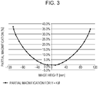
- Fig. 13 illustrates an example in which the rate of change in scanning velocity C is 35% and thus a partial magnification of 35% is generated at the most off-axis image height when the on-axis image height is a reference.
- the partial magnification correction information 314 indicates that the point of 17% corresponds to zero magnification correction, the most off-axis image height corresponds to -18% (-18/100), and the on-axis image height corresponds to +17% (+17/100).
- the partial magnification correction information 314 indicates that the point of 17% corresponds to zero magnification correction, the most off-axis image height corresponds to -18% (-18/100), and the on-axis image height corresponds to +17% (+17/100).
- the brightness correction value 315 that is generated by the CPU core 2 on the basis of the partial magnification characteristic information 317 and the correction current information is set so that the current value Id decreases as the absolute value of the image height Y increases.
- the current IL increases as the absolute value of the image height Y increases. In other words, during one scanning operation, the current value Id changes, and the current IL decreases toward the center portion of the image (as the absolute value of the image height Y decreases).
- the amount of laser light output from the light emitter 11 is corrected so that the light emitter 11 emits light with the brightness Papc1 at the most off-axis image height and emits light with a brightness 0.74 times the brightness Papc1, as illustrated in Fig. 13 .
- the laser light is attenuated at an attenuation ratio of 26%. That is, the brightness at the most off-axis image height is 1.35 times the brightness at the on-axis image height.
- An input of the DA converter 21 and the rate of decrease in brightness have a proportional relationship. For example, in a case where a setting is made so that an input of the DA converter 21 in the CPU core 2 is FFh and the amount of light decreases by 26%, the amount of light decreases by 13% at 80h.
- the irradiation period is shortened, that is, the irradiation period at the intermediate image height is 0.87 times T3, and the irradiation period at the most off-axis image height is 0.74 times T3, and thus the peak of the integrated amount of light is further lowered compared to Fig. 4A .
- partial magnification correction and brightness correction are performed, and accordingly exposure can be performed while suppressing the occurrence of image failure without using a scanning lens having an f ⁇ characteristic.
- partial magnification correction can be performed without changing the clock frequencies of the clock signal 125 and the clock signal 126.
- partial magnification correction can be performed only by providing one clock generating unit, and an increase in the cost of a clock generating unit can be suppressed.
- partial magnification correction can be performed by inserting or extracting pixel pieces, and thus a relatively high accuracy of partial magnification correction can be achieved.
- the memory 304 stores only partial magnification characteristic information.
- the correction current for the light emitter 11, which is calculated by using the partial magnification characteristic information and is used to obtain target brightness is calculated by using a laser brightness monitoring unit of the laser driving unit 300 under control by the apparatus.
- the partial magnification correction and the other configuration are the same as those in the first exemplary embodiment, and thus the same reference numerals are assigned and the description thereof is omitted.
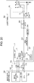
- Fig. 14 is an electric block diagram illustrating an exposure control configuration.
- the laser driving unit 300 according to this exemplary embodiment ( Fig. 14 ) is different from the laser driving unit 300 according to the first exemplary embodiment ( Fig. 5 ) in that a VI conversion circuit 318 has a different function from that of the VI conversion circuit 306 and that a buffer circuit 320 is provided. Further, an IC 20 of the control unit 1 includes an AD converter.
- the buffer circuit 320 is used to buffer a voltage obtained by converting, with the variable resistor 13, a current generated at the photodetector 12 in accordance with the emission brightness of the light emitter 11, and transmit the buffered voltage to the IC 20 of the control unit 1.
- the VI conversion circuit 318 has a characteristic in which the direction of a current output therefrom is opposite to that in the first exemplary embodiment.
- the memory 304 stores only partial magnification characteristic information.
- the elements other than the above-described circuit and device are the same as those in the first exemplary embodiment, and are thus denoted by the same reference numerals and the description thereof is omitted.
- the IC 20 including the CPU core 2 calculates a brightness correction value, and outputs the brightness correction analog voltage 312 that increases/decreases in the main scanning in synchronization with the BD signal 111 as a horizontal synchronization signal.
- the brightness correction analog voltage 312 is determined by the brightness correction value 315 generated by the CPU core 2 in the IC 20 and the reference voltage 23 of the DA converter 21 output from the regulator 22.
- the brightness can be increased to 1.35 times Papc2 (points B and D in Fig. 15 ).
- the output current 313 of the VI conversion circuit 318 gradually increases in accordance with change of a laser light irradiation position from the center portion (on-axis image height) to the end portion (most off-axis image height), so that a laser current is increased and the brightness of the light emitter 11 is increased.
- This processing flow is performed by the CPU core 2 when the power of the image-forming apparatus 9 is turned on for the first time and is stored in the memory 304. When the power is turned on thereafter, the CPU core 2 refers to a value stored in the memory 304. Alternatively, the CPU core 2 may perform the processing flow every time the power is turned on or may perform the processing flow at a recovery from a standby mode.
- the CPU core 2 of the IC 20 inputs 00h to the DA converter 21 so that an output voltage is 0 V (steps S1 and S2).
- the laser driver IC 16 automatically adjusts the laser current IL so that laser light is output with a certain brightness (step S3).
- the image modulating unit 101 continuously keeps the VDO signal 110 in an ON-state, and the CPU core 2 captures a voltage Von as a PD monitor voltage 319 (step S4).
- the image modulating unit 101 continuously keeps the VDO signal 110 in an OFF-state, and the CPU core 2 captures a voltage Voff as the PD monitor voltage 319 (steps S5 and S6).
- the image modulating unit 101 causes the VDO signal 110 to be in an ON-state (step S9).
- the CPU core 2 sets the input of the DA converter 21 to FFh (step S10).
- the CPU core 2 increments the reference voltage 23 represented by VrefH output from the regulator 22 from 0 V, and compares the reference voltage 23 with the target voltage Va with reference to the PD monitor voltage 319 (steps S11 and S12).
- the CPU core 2 stores, in the memory 304, the reference voltage 23 of the DA converter 21 when the PD monitor voltage 319 matches Va, that is, the set value of the regulator 22 (step S13). As illustrated in Fig.
- the laser current and the brightness have a proportional relationship.
- the brightness increases by 17.5% by inputting half of FFh, that is, 80h.
- the main scanning LSF profile can be corrected so that an image is not affected.
- an illumination (emission) period and brightness of the light source 401 controlled by using the VDO signal 110 are made more appropriate so as to achieve optimal image formation for a fine image constituted by lines (vertical lines) extending in the sub-scanning direction with a width of one pixel (dot), for example.
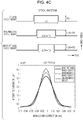
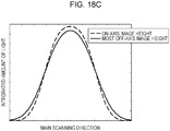
- Figs. 18A to 18C illustrate main scanning LSF profiles obtained as a result of performing laser scanning for one dot in a case where the same partial magnification correction and brightness correction as those in the first exemplary embodiment are performed.
- Fig. 18A illustrates a main scanning LSF profile of the on-axis image height
- Fig. 18B illustrates a main scanning LSF profile of the most off-axis image height
- Fig. 18C illustrates the main scanning LSF profiles of one dot of the on-axis image height and the most off-axis image height illustrated in Figs. 18A and 18B in an overlapped manner.
- the resolution is 600 dpi
- the width in the main scanning direction of one dot (pixel) is 42.3 ⁇ m.
- the main scanning LSF profile of one dot differs between the on-axis image height and the most off-axis image height. This is because the profiles of stationary spots represented by broken lines in Figs. 18A and 18B differ between the on-axis image height and the most off-axis image height.
- the profile of a stationary spot is a main scanning LSF profile formed by a laser spot at a certain moment. As a result of summing up the profiles of stationary spots at individual main scanning positions, the main scanning LSF profiles of one dot represented by solid lines in Figs. 18A and 18B are obtained.
- emission period correction and brightness correction for the light source 401 are performed on the basis of the VDO signal 110, in addition to the partial magnification correction according to the first exemplary embodiment, and thereby the reproducibility of a fine image is further enhanced.
- Figs. 19A and 19B are diagrams illustrating optical waveforms and main scanning LSF profiles. These optical waveforms and main scanning LSF profiles are obtained in a case where the light source 401 emits light with a certain brightness for a certain period at the on-axis image height, the intermediate image height, and the most off-axis image height.
- Fig. 19A illustrates a main scanning LSF profile in a case where the partial magnification correction and brightness correction according to the first exemplary embodiment are performed
- Fig. 19B illustrates a main scanning LSF profile in a case where correction according to this exemplary embodiment is performed.
- T3 represents a period that is necessary for main-scanning one pixel (42.3 ⁇ m) at the on-axis image height.
- Fig. 19A and 19B are diagrams illustrating optical waveforms and main scanning LSF profiles. These optical waveforms and main scanning LSF profiles are obtained in a case where the light source 401 emits light with a certain brightness for a certain period at the
- FIG. 19A illustrates a case where the emission period of laser is T3 and the brightness is P3 at the on-axis image height, and the emission period for an amount of emitted laser light 170 is 0.74 times T3 and the emission brightness is 1.35 times P3 at the most off-axis image height.
- Fig. 19B illustrates a case where correction is performed through the processing described below so that the emission period is 0.22 times T3 and the emission brightness is 4.5 times P3 at the most off-axis image height.
- the main scanning LSF profiles of laser scanning for one dot can be made more similar to each other between the on-axis image height and the most off-axis image height.
- the interval between dots of adjacent pixels needs to be maintained in a state equivalent to a state where the partial magnification correction according to the first exemplary embodiment is performed.
- the period corresponding to one dot (pixel) is 0.74 ⁇ T3 at the most off-axis image height, and 0.87 ⁇ T3 at the intermediate image height.
- emission period correction is performed by using the halftone processing unit 122 serving as a screen processing unit, with the partial magnification correction according to the first exemplary embodiment being performed.
- a correction constant for the brightness correction described above in the first exemplary embodiment is set to a value in consideration of emission period correction.
- Emission period correction is performed by a halftone processing unit 186 of the image modulating unit 160 illustrated in Fig. 21 .
- the halftone processing unit 186 stores screens corresponding to individual image heights, selects a screen on the basis of information output from a screen (SCR) switching unit 185, and performs halftone processing.
- the SCR switching unit 185 generates screen switching information 184 by using the BD signal 111 serving as a synchronization signal and the image clock signal 125.
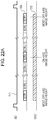
- Fig. 22A is a diagram illustrating screens corresponding to individual image heights.
- the SCR switching unit 185 outputs the screen switching information 184 in accordance with an image height in the main scanning direction, as illustrated in Fig. 22A .
- the screen switching information 184 is a first screen SCR1 at the most off-axis image height, and is an n-th screen SCRn at the on-axis image height.
- the halftone processing unit 186 and the SCR switching unit 185 function as an emission period correcting unit.
- Fig. 22B illustrates an example of the n-th screen that is used near the on-axis image height
- Fig. 22C illustrates an example of the first screen that is used near the most off-axis image height
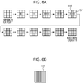
- Each of the screens is constituted by a matrix formed of two hundred lines
- the gradation of each pixel can be expressed by sixteen pixel pieces that are obtained by dividing the pixel
- the area of the screen constituted by nine pixels grows in accordance with density information represented by 8-bit multivalued parallel data of the VDO signal 110.
- the matrix 153 is provided for each gradation level, and the gradation level increases (the density increases) in the order indicated by arrows.
- the first screen is set so that not all the sixteen pixel pieces are illuminated even in the matrix of the highest gradation level (maximum density).
- the maximum emission period at the most off-axis image height is set to 0.22 * T3, with T3 at the on-axis image height being a reference.
- the emission period corresponding to one dot (pixel) is limited to 0.74 ⁇ T3.
- up to about five pixel pieces may be illuminated in the screen.
- Brightness correction can be performed by changing a correction constant. That is, the reference voltage 23 to be input to the DA converter 21 illustrated in the electric block diagram in Fig. 5 according to the first exemplary embodiment may be changed, and thus the description thereof is omitted.
- Fig. 23 is a timing chart of the processing according to this exemplary embodiment.
- An amount of correction at the off-axis image height for a brightness correction analog voltage 330, a VI conversion output current Id 331, and an amount of emitted laser light 332 is larger than in the first exemplary embodiment.
- the brightness at the on-axis image height is equivalent to that in the first exemplary embodiment, but the brightness at the most off-axis image height is 4.5 times in this exemplary embodiment, though it is 1.35 times in the first exemplary embodiment.
- the brightness P3 at the on-axis image height is 0.22 times the brightness P3' (100%/450%).
- the emission period and emission brightness of the light source 401 are corrected through partial magnification correction, emission period correction, and brightness correction.
- the following condition is necessary to make the density of an image constant in the main scanning direction. That is, as indicated by the optical waveforms illustrated in Figs. 19A and 19B , the value obtained by integrating an emission brightness with an emission period is the same or substantially the same at the on-axis image height, intermediate image height, and most off-axis image height.
- the integrals at the individual image heights are as follows.
- the emission period of the light source 401 is shortened and the brightness thereof is increased compared to the first exemplary embodiment so that the main scanning LSF profiles of one dot match each other.
- a correction amount between the amount according to the first exemplary embodiment and the amount according to the third exemplary embodiment may be used. Further, the correction amount may be changed in accordance with the type of an image to be printed. For example, in the case of an ordinary image, partial magnification correction and brightness correction may be performed as in the first exemplary embodiment. In the case of an image using many thin lines, partial magnification correction, emission period correction, and brightness correction may be performed as in the third exemplary embodiment.
- partial magnification correction and brightness correction are performed, and thus exposure can be performed while suppressing the occurrence of image failure without using a scanning lens having an f ⁇ characteristic.
- emission period correction is performed in which the ratio of an emission period among periods assigned to individual pixels that have undergone partial magnification correction is decreased from the on-axis image height to the most off-axis image height.
- emission brightness is increased by performing brightness correction. Accordingly, even a thin-line image constituted by vertical lines having a width of one dot can be printed with good image quality.
- the other parts, such as partial magnification correction, is the same as in the first exemplary embodiment.
- the same parts as those in the first exemplary embodiment are denoted by the same reference numerals, and the description thereof is omitted.
- Fig. 24 is an electric block diagram illustrating an exposure control configuration in the image-forming apparatus 9.
- the image signal generating unit 100 receives print information from the host computer (not illustrated) and generates the VDO signal 110 corresponding to image data (image signal). Also, the image signal generating unit 100 has a function of a pixel width correcting unit and a function as a density correcting unit for correcting image density.
- the control unit 1 controls the image-forming apparatus 9.
- the laser driving unit 300 includes the memory 304, the laser driver IC 16, and the light emitter 11 of the light source 401.
- the laser driver IC 16 switches, in accordance with the VDO signal 110, whether to supply the current IL to the light emitter 11 to cause the light emitter 11 to emit light or to supply a dummy resistance 10 to the light emitter 11 to turn off the light emitter 11, so as to control ON/OFF of light emission of the light source 401 on the basis of the VDO signal 110.
- the photodetector 12 detects the amount of light emitted by the light emitter 11.
- the image signal generating unit 100 instructs the control unit 1 to start printing through serial communication 113.
- the control unit 1 includes the CPU core 2.
- the CPU core 2 transmits the TOP signal 112 serving as a sub-scanning synchronization signal and the BD signal 111 serving as a main scanning synchronization signal to the image signal generating unit 100.
- the image signal generating unit 100 outputs the VDO signal 110 serving as an image signal to the laser driving unit 300 at a certain timing.
- Fig. 26 is a timing chart illustrating an example of the above-described partial magnification correction.
- the memory 304 illustrated in Fig. 24 stores the partial magnification characteristic information 317 about the optical scanning device 400.
- the partial magnification characteristic information may be measured and stored for each device after the optical scanning device 400 has been assembled. In a case where there is a small variation among the individual devices, a representative characteristic may be stored without measurement of information for the individual devices.
- the CPU core 2 reads the partial magnification characteristic information 317 from the memory 304 through serial communication 307, and transmits it to the CPU 102 in the image signal generating unit 100.
- the CPU core 2 On the basis of the information, the CPU core 2 generates the partial magnification correction information 314, and transmits it to the pixel piece insertion/extraction controller 128 in the image modulating unit 101 illustrated in Fig. 24 .
- Partial magnification correction is the same as in the first exemplary embodiment.
- Fig. 26 illustrates an example in which the rate of change in scanning velocity C is 35% and thus partial magnification of 35% is generated at the most off-axis image height when the on-axis image height is a reference.
- the partial magnification correction information 314 indicates that the point of 17% corresponds to zero magnification correction, the most off-axis image height corresponds to -18% (-18/100), and the on-axis image height corresponds to +17% (+17/100).
- pixel pieces are extracted to decrease an image length near the end portion where the absolute value of the image height is large, and pixel pieces are inserted to increase an image length near the center portion where the absolute value of the image height is small.
- pixel pieces are extracted to increase an image length near the center portion where the absolute value of the image height is small.
- eighteen pixel pieces are extracted from one hundred pixel pieces.
- seventeen pixel pieces are inserted into one hundred pixel pieces.
- the state near the most off-axis image height (end portion) is substantially the same as a state where thirty-five pixel pieces are extracted from one hundred pixel pieces, and accordingly partial magnification of 35% can be corrected. That is, the time period over which the spot of the laser light 208 is moved a distance corresponding to the width of one pixel (42.3 ⁇ m (600 dpi)) on the scanned surface 407 at the most off-axis image height is 0.74 times that at the on-axis image height.
- the pixel width (pixel interval) can be corrected, and latent images corresponding to individual pixels can be formed with a substantially uniform interval in the main scanning direction. That is, if a pixel piece is extracted, a pixel interval decreases and an emission interval of laser light decreases. If a pixel piece is inserted, a pixel interval increases and an emission interval of laser light increases. Thus, more pixel pieces are extracted as the scanning velocity increases, and/or more pixel pieces are inserted as the scanning velocity decreases, and accordingly the emission timing of laser light can be corrected so that latent image dots of laser light can be formed with a substantially uniform interval in the main scanning direction. Accordingly, partial magnification can be corrected. In this way, the pixel piece insertion/extraction controller 128 functions as an emission timing correcting unit that corrects an emission timing.
- the on-axis image height may be regarded as a reference, neither insertion nor extraction of a pixel piece may be performed near the on-axis image height, and the rate of extracting pixel pieces may be increased as the image height approaches the most off-axis image height.
- the most off-axis image height may be regarded as a reference, neither insertion nor extraction of a pixel piece may be performed near the most off-axis image height, and the rate of inserting pixel pieces may be increased as the image height approaches the on-axis image height.
- density correction processing for correcting, with image processing, variation of density caused by an integrated amount of light that is decreased by shortening an irradiation period of a light source from the on-axis image height to the most off-axis image height through partial magnification correction.
- the density correction processing the density of an image is corrected so that the density becomes uniform from the on-axis image height to the off-image image height in the main scanning direction.
- Fig. 27 is a flowchart illustrating density correction processing according to the fourth exemplary embodiment.
- the density correction processing is performed by the image modulating unit 101.
- a density correction value stored in the memory 304 (see Fig. 24 ) is read (step S1).
- the density correction value stored in the memory 304 may be measured and stored in each device. Alternatively, a representative characteristic may be stored at the time of manufacturing without individually measuring values.
- the density correction value stored in the memory 304 is transmitted to the control unit 1 through serial communication 307, is further transmitted to the image modulating unit 101 of the image signal generating unit 100 through serial communication 113, and is stored in the density correcting unit 121 (see Fig. 7 ).
- the density correcting unit 121 performs density correction processing on image data by using the stored density correction value (step S2).
- the density correcting unit 121 is an emission ratio correcting unit that corrects image density of a printed image by correcting the emission ratio of laser light emitted by the light source 401.
- the density correcting unit 121 reads the density correction value in synchronization with the BD signal 111, and performs correction to decrease an image gradation value from the off-axis image height to the on-axis image height so as to prevent a decrease in image density caused by a decrease in the total amount of exposure per unit length from the on-axis image height to the off-axis image height due to a decrease in the amount of exposure.
- the image density is made uniform at the on-axis image height and the off-axis image height.
- image density is a value for each pixel that is obtained by measuring the toner density of a printed image.
- FIG. 26 is a timing chart illustrating an example of the above-described density correction.
- a density correction value 321 is a value read from the memory 304.
- the density correction value 321 varies according to an image height, and is thus not constant in a print region.
- a reference image density is the image density at the most off-axis image height.
- the image density increases from the most off-axis image height to the on-axis image height.
- the processing of decreasing image density from the most off-axis image height to the on-axis image height so as to uniform the image density in the main scanning direction.
- the density correction value 321 corresponds to a range of reduction (value) in density.
- the processing of gradually decreasing the density from the most off-axis image height to the on-axis image height is performed, and thus the density correction value gradually increases from the most off-axis image height to the on-axis image height.
- Changing of density is changing of a screen as illustrated in Fig. 8A , and is synonymous with changing of the emission ratio of laser light emitted by the light source 401.
- the density correction value 321 is a value indicating the number of levels of density to be decreased from the image density value of 256 levels of gradation of image data.
- the density correction value 321 can be expressed by a hexadecimal number, like the density levels of image data.
- a print region is divided into three regions in the main scanning direction, and the density correction value 321 is assigned to each region.
- the three regions include a region near the most off-axis image height, a region near the on-axis image height, and an intermediate image height region between the region near the most off-axis image height and the region near the on-axis image height.
- the region near the most off-axis image height is a region where the density is not changed, a density correction value "00h” is assigned thereto, and the amount of correction for decreasing density corresponds to zero levels of gradation.
- a density correction value "07h” is assigned to decrease the image density by 2.7%, and the density is corrected so as to be decreased by seven levels of gradation.
- a density correction value "0Fh” is assigned to decrease the image density by 5.8%, and the density is corrected so as to be decreased by sixteen levels of gradation.
- an image density value before density correction 311 is performed is an image density value input to the density correcting unit 121 (see Fig. 7 ).
- An image density value in image data is a value corresponding to the density of a toner image formed on the photosensitive drum 4.
- Fig. 26 illustrates a case where the image density value input to the density correcting unit 121 is at the highest level "FFh" in all the regions (image heights) of the print region.
- the density correcting unit 121 performs density correction processing by using the density correction value 321 and the image density value 311.
- a value “F8h” obtained by subtracting the density correction value "07h” from the image density value "FFh” is an image density value after density correction 310.
- a value “F0h” obtained by subtracting the density correction value "0Fh” from the image density value "FFh” is the image density value after density correction 310.
- the density correcting unit 121 performs correction so that the density of the image decreases as the scanning velocity decreases.
- Figs. 25A to 25C illustrate an example of a screen on which density correction processing is performed and then halftone processing is performed.
- Each screen is a matrix constituted by three pixels in the main scanning direction and three pixels in the sub-scanning direction and including two hundred lines.
- the area ratio of a portion illuminated by the light source 401 (black portion) to the entire area is 100%.
- the area ratio is 93% in a screen 121, and the area ratio is 85% in a screen 122.
- the area ratio is a light emission ratio in the screen.
- the screen 120 is assigned to the region where the image density value after density correction 310 is "FFh”
- the screen 121 is assigned to the region where the image density value after density correction 310 is "F8h”
- the screen 122 is assigned to the region where the image density value after density correction 310 is "F0h”.
- PS conversion is performed by the PS conversion unit 123
- the processing is performed by the FIFO 124
- the VDO signal 110 is output to the laser driving unit 300
- the light source 401 emits light.
- the density correcting unit 121 functions as an emission ratio correcting unit that corrects the emission ratio of laser light emitted by the light source 401.
- the density correcting unit 121 performs correction so that the density of an image decreases as the scanning velocity decreases.
- the density correcting unit 121 may perform correction so that the density of an image increases as the scanning velocity increases.
- the density correcting unit 121 may perform correction so that the density of an image increases as the scanning velocity increases while performing correction so that the density of an image decreases as the scanning velocity decreases.
- partial magnification correction and density correction for correcting image density of image data are performed, and accordingly exposure can be performed while suppressing the occurrence of image failure without using a scanning lens having an f ⁇ characteristic.
- partial magnification correction is performed by inserting or extracting pixel pieces.
- partial magnification correction may be performed by correcting the emission timing of laser light by changing a clock frequency in the main scanning direction, as disclosed in Japanese Patent Laid-Open No. 58-125064 .
- the following effect can be obtained compared to the method of changing a clock frequency in the main scanning direction disclosed in Japanese Patent Laid-Open No. 58-125064 . That is, in the configuration disclosed in Japanese Patent Laid-Open No.
- a clock frequency is changed in the main scanning direction, and thus a clock generating unit capable of outputting clock signals of a plurality of different frequencies is necessary, which causes an increase in cost.
- partial magnification correction can be performed only by providing one clock generating unit, and thus the cost for a clock generating unit can be reduced.
- the fifth exemplary embodiment is different from the fourth exemplary embodiment in the density correction method, but is the same as the fourth exemplary embodiment regarding the partial magnification correction and so forth.
- the same parts as those in the fourth exemplary embodiment are denoted by the same reference numerals, and the description thereof is omitted.
- the image density value of image data is not corrected, but the density of an image is corrected by performing forced OFF processing, in which the light source 401 is forcibly turned off with high resolution in units of pixel pieces each having a width smaller than the width of one pixel.
- Fig. 28 is a block diagram illustrating an example of the image modulating unit 101 according to the fifth exemplary embodiment.
- a forced OFF processing unit 133 is provided between the halftone processing unit 122 and the PS conversion unit 123.
- the forced OFF processing unit 133 performs processing of forcibly turning OFF the light source 401.
- the forced OFF processing unit 133 corresponds to a correcting unit that substantially corrects the image density of a printed image.
- step S1 a processing value for forced OFF processing is read from the memory 304, as in the case of the density correction value according to the fourth exemplary embodiment.
- the read processing value is stored in the forced OFF processing unit 133.
- step S2 the forced OFF processing unit 133 performs forced OFF processing in units of one-sixteenth of a pixel on the basis of the processing value.
- one pixel is constituted by sixteen pixel pieces formed by dividing one dot of 600 dpi into sixteen pieces.
- the above-described processing value is a value corresponding to the number of pixel pieces for which the light source 401 is forcibly turned off.
- the forced OFF processing is processing of forcibly turning off the sixteen pixel pieces, which are obtained by dividing one pixel into sixteen pieces in the main scanning direction, at a certain rate (frequency) in the main scanning direction.
- FIG. 30A to 30C is a diagram illustrating emission data of one pixel on which forced OFF processing has been performed in a case where the image density value of image data before forced OFF processing is FFh.
- Fig. 30A illustrates emission data of one pixel in a case where the number of pixel pieces as a target of forced OFF processing is zero.
- Fig. 30B illustrates emission data of one pixel in a case where the number of pixel pieces as a target of forced OFF processing is one.
- Fig. 30C illustrates emission data of one pixel in a case where the number of pixel pieces as a target of forced OFF processing is two.
- the emission data of one pixel illustrated in Fig. 30A is obtained in a case where the processing value is zero
- the emission data of one pixel illustrated in Fig. 30B is obtained in a case where the processing value is one
- the emission data of one pixel illustrated in Fig. 30C is obtained in a case where the processing value is two.
- the processing value of forced OFF processing is set so that the number of pixel pieces as a target of forced OFF processing increases from the most off-axis image height to the on-axis image height (from the end portion to the center portion of the print region).
- a 16-bit parallel signal 134 is output to the PS conversion unit 123. After that, the same processing as in the fourth exemplary embodiment is performed.
- Fig. 29 is a timing chart illustrating a case where partial magnification correction and forced OFF processing are performed.
- an image density value 162 of image data is FFh.
- the number of pixel pieces in one pixel to be forcibly turned off by the forced OFF processing unit 133 is illustrated as a processing value 163.
- a density of a printed image 164 is an image density that is obtained by performing the above-described partial magnification correction and forced OFF processing, and is an image density obtained by measuring the image density after printing.
- the forced OFF processing unit 133 corrects emission data so that the density of an image decreases as the scanning velocity decreases. Accordingly, the image can be printed by substantially decreasing the image density, and finally an appropriate image density can be obtained from the most off-axis image height to the on-axis image height.
- the image density value of the image data is constant in the main scanning direction
- the image density can be made constant in the main scanning direction, as can be seen in the density of the printed image 164 after correction illustrated in Fig. 29 .
- the pixel piece for which forced OFF processing is performed may be any pixel piece of one pixel.
- the processing value for forced OFF processing is 2 or more and a plurality of pixel pieces in one pixel are to be forcibly turned off, a more uniform image density can be obtained by disposing, between pixel pieces subjected to forced OFF processing, at least one pixel piece not subjected to forced OFF processing.
- the processing value for forced OFF processing may be a value smaller than 1. For example, in a case where the processing value is 0.5, one pixel piece in two pixels contiguous in the main scanning direction is forcibly turned off.
- partial magnification correction and forced OFF processing are performed, and thereby exposure can be performed while suppressing the occurrence of image failure without using a scanning lens having an f ⁇ characteristic.
- both of the density correction processing according to the fourth exemplary embodiment and the forced OFF processing according to the fifth exemplary embodiment are performed to decrease image density from off-axis to on-axis so as to optimize the image density, in a situation where the image density is decreased from on-axis to off-axis due to a decrease in the amount of exposure.
- the same parts as those in the fourth and fifth exemplary embodiments are denoted by the same reference numerals, and the description thereof is omitted.
- both of the density correction processing and the forced OFF processing as in this exemplary embodiment is appropriate in a case where only one of the density correction processing and the forced OFF processing is insufficient to cope with change in density caused by change in scanning velocity due to a high rate of change in scanning velocity or other reasons.
- Fig. 32 is a block a block diagram illustrating an example of the image modulating unit 101 according to the sixth exemplary embodiment.
- the forced OFF processing unit 133 for forcibly turning OFF the light source 401 is provided between the halftone processing unit 122 and the PS conversion unit 123.
- step S1 a correction value is read from the memory 304.
- the correction value is 16-bit data.
- the upper 8 bits of the correction value correspond to the density correction value according to the fourth exemplary embodiment used by the density correcting unit 121, and are stored in in the density correcting unit 121.
- the lower 8 bits correspond to the processing value according to the fifth exemplary embodiment used by the forced OFF processing unit 133, and are stored in the forced OFF processing unit 133.
- step S2 the same density correction processing as in the fourth exemplary embodiment is performed by using the stored upper 8 bits of the correction value.
- step S3 halftone processing is performed by the same halftone processing unit 122 as that in the fourth exemplary embodiment.
- step S4 forced OFF processing is performed by the same forced OFF processing unit 133 as that in the fifth exemplary embodiment.
- the lower 8 bits of the correction value correspond to the number of pixel pieces for which forced OFF processing is performed by the forced OFF processing unit 133.
- the lower 8 bits of the correction value correspond to 01h
- one pixel piece having a 1/16 width of each pixel is forcibly turned off in each pixel.
- the lower 8 bits of the correction value correspond to 02h
- two pixel pieces in each pixel are forcibly turned off.
- FIG. 34A to 34C is a diagram illustrating a screen (corresponding to emission data of a plurality of pixels) on which halftone processing is performed after density correction processing and forced OFF processing have been performed in a case where the image density value of image data before forced OFF processing is FFh.
- Fig. 34A illustrates a case where density correction processing and forced OFF processing are not performed
- Fig. 34B illustrates a case where the correction value is 0701h
- Fig. 34C illustrates a case where the correction value is 0F02h.
- the 16-bit parallel signal 134 is output to the PS conversion unit 123. After that, the same processing as in the fourth exemplary embodiment is performed.
- Fig. 33 is a timing chart of a case where partial magnification correction, density correction processing, and forced OFF processing are performed.
- the image density value 162 of image data is FFh.
- the image density value of the image data after the density correcting unit 12 has corrected the density is the image density value 202 of the image data.
- the number of pixel pieces in one pixel that are forcibly turned OFF by the forced OFF processing unit 133 is indicated as the processing value 203.
- the density of the printed image 164 is an image density of an image printed after the above-described partial magnification correction and forced OFF processing have been performed, and is an image density obtained through measurement after printing.
- an image can be printed by substantially decreasing the image density, and finally an appropriate image density can be obtained from the most off-axis image height to the on-axis image height.
- the image density can be made constant in the main scanning direction as indicated by the density of the printed image 164 after correction illustrated in Fig. 33 .
- the pixel piece to be forcibly turned off may be any pixel piece of one pixel.
- the processing value for forced OFF processing is 2 or more and a plurality of pixel pieces in one pixel are to be forcibly turned off, a more uniform image density can be obtained by disposing, between pixel pieces subjected to forced OFF processing, at least one pixel piece not subjected to forced OFF processing.
- the correspondence between the lower 8 bits of the correction value and the processing value for forced OFF processing is not limited to the one described above, and may be appropriately set.
- the processing value for forced OFF processing may be a value smaller than 1. For example, in a case where the processing value is 0.5, one pixel piece in two pixels contiguous in the main scanning direction is forcibly turned off.
- the image height at which the density correction value changes need not be the same as the image height at which the processing value of forced OFF processing changes.
- the density correction value and processing value may be appropriately set in consideration of gradation of image data, density characteristic, and so forth.
- partial magnification correction, density correction processing, and forced OFF processing are performed, and thereby exposure can be performed while suppressing the occurrence of image failure without using a scanning lens having an f ⁇ characteristic.
- An image-forming apparatus (9) that includes a light-irradiation means configured to irradiate a surface of a charged photosensitive member with laser light emitted by a light source in accordance with image data so that a spot
Landscapes
- Engineering & Computer Science (AREA)
- Multimedia (AREA)
- Signal Processing (AREA)
- Physics & Mathematics (AREA)
- General Physics & Mathematics (AREA)
- Facsimile Scanning Arrangements (AREA)
- Laser Beam Printer (AREA)
- Optics & Photonics (AREA)
- Mechanical Optical Scanning Systems (AREA)
Priority Applications (1)
| Application Number | Priority Date | Filing Date | Title |
|---|---|---|---|
| EP22192310.5A EP4141558A1 (fr) | 2014-06-12 | 2015-05-28 | Appareil de formation d'images |
Applications Claiming Priority (3)
| Application Number | Priority Date | Filing Date | Title |
|---|---|---|---|
| JP2014121882A JP6261452B2 (ja) | 2014-06-12 | 2014-06-12 | 画像形成装置 |
| JP2014121883A JP6261453B2 (ja) | 2014-06-12 | 2014-06-12 | 画像形成装置 |
| EP15169666.3A EP2955585B1 (fr) | 2014-06-12 | 2015-05-28 | Appareil de formation d'image |
Related Parent Applications (2)
| Application Number | Title | Priority Date | Filing Date |
|---|---|---|---|
| EP15169666.3A Division-Into EP2955585B1 (fr) | 2014-06-12 | 2015-05-28 | Appareil de formation d'image |
| EP15169666.3A Division EP2955585B1 (fr) | 2014-06-12 | 2015-05-28 | Appareil de formation d'image |
Related Child Applications (2)
| Application Number | Title | Priority Date | Filing Date |
|---|---|---|---|
| EP22192310.5A Division EP4141558A1 (fr) | 2014-06-12 | 2015-05-28 | Appareil de formation d'images |
| EP22192310.5A Division-Into EP4141558A1 (fr) | 2014-06-12 | 2015-05-28 | Appareil de formation d'images |
Publications (2)
| Publication Number | Publication Date |
|---|---|
| EP3722880A1 true EP3722880A1 (fr) | 2020-10-14 |
| EP3722880B1 EP3722880B1 (fr) | 2022-10-05 |
Family
ID=53264598
Family Applications (3)
| Application Number | Title | Priority Date | Filing Date |
|---|---|---|---|
| EP22192310.5A Pending EP4141558A1 (fr) | 2014-06-12 | 2015-05-28 | Appareil de formation d'images |
| EP20169718.2A Active EP3722880B1 (fr) | 2014-06-12 | 2015-05-28 | Appareil de formation d'image |
| EP15169666.3A Active EP2955585B1 (fr) | 2014-06-12 | 2015-05-28 | Appareil de formation d'image |
Family Applications Before (1)
| Application Number | Title | Priority Date | Filing Date |
|---|---|---|---|
| EP22192310.5A Pending EP4141558A1 (fr) | 2014-06-12 | 2015-05-28 | Appareil de formation d'images |
Family Applications After (1)
| Application Number | Title | Priority Date | Filing Date |
|---|---|---|---|
| EP15169666.3A Active EP2955585B1 (fr) | 2014-06-12 | 2015-05-28 | Appareil de formation d'image |
Country Status (4)
| Country | Link |
|---|---|
| US (4) | US9319553B2 (fr) |
| EP (3) | EP4141558A1 (fr) |
| KR (1) | KR101890016B1 (fr) |
| CN (2) | CN105319892B (fr) |
Families Citing this family (16)
| Publication number | Priority date | Publication date | Assignee | Title |
|---|---|---|---|---|
| JP6551150B2 (ja) * | 2015-10-23 | 2019-07-31 | 株式会社リコー | 画像処理装置、画像形成装置、及び画像処理方法 |
| JP2017083511A (ja) * | 2015-10-23 | 2017-05-18 | 京セラドキュメントソリューションズ株式会社 | 光走査装置およびこれを備える画像形成装置 |
| JP6230586B2 (ja) * | 2015-11-26 | 2017-11-15 | キヤノン株式会社 | 光走査装置及びそれを備える画像形成装置 |
| US9927735B2 (en) * | 2016-04-28 | 2018-03-27 | Canon Kabushiki Kaisha | Image forming apparatus that divides one pixel into plurality of pixel pieces and performs exposure on pixel piece-by-pixel piece basis |
| JP6706144B2 (ja) | 2016-05-27 | 2020-06-03 | キヤノン株式会社 | 画像形成装置 |
| JP6821340B2 (ja) | 2016-06-30 | 2021-01-27 | キヤノン株式会社 | 画像形成装置 |
| JP2018086781A (ja) * | 2016-11-29 | 2018-06-07 | キヤノン株式会社 | 画像形成装置 |
| JP6649630B2 (ja) * | 2016-12-22 | 2020-02-19 | 京セラドキュメントソリューションズ株式会社 | 光走査装置及びこれを備えた画像形成装置 |
| JP6918486B2 (ja) * | 2016-12-27 | 2021-08-11 | キヤノン株式会社 | 画像形成装置 |
| JP2019124873A (ja) | 2018-01-18 | 2019-07-25 | キヤノン株式会社 | 画像形成装置およびその制御方法 |
| JP2019200376A (ja) * | 2018-05-18 | 2019-11-21 | キヤノン株式会社 | 走査装置及び画像形成装置 |
| US10747139B1 (en) * | 2019-09-10 | 2020-08-18 | Toshiba Tec Kabushiki Kaisha | Control circuit, image forming apparatus, and control method |
| CN112068264B (zh) * | 2020-09-24 | 2022-07-12 | 福建师范大学 | 一种高功率激光光束匀化耦合装置 |
| JP2022057608A (ja) * | 2020-09-30 | 2022-04-11 | キヤノン株式会社 | 画像形成装置 |
| CN112884093B (zh) * | 2021-04-29 | 2021-08-31 | 四川大学 | 基于dscrn模型的旋转机械故障诊断方法、设备和存储介质 |
| CN114274657B (zh) * | 2021-12-22 | 2023-01-31 | 深圳市先地图像科技有限公司 | 一种激光直接制版控制方法、系统及相关设备 |
Citations (6)
| Publication number | Priority date | Publication date | Assignee | Title |
|---|---|---|---|---|
| JPS58125064A (ja) | 1982-01-20 | 1983-07-25 | Sharp Corp | レ−ザプリンタ |
| JPH02131212A (ja) * | 1988-11-11 | 1990-05-21 | Minolta Camera Co Ltd | レーザビームの走査速度補正方式 |
| JPH063911A (ja) * | 1992-06-19 | 1994-01-14 | Canon Inc | 画像形成装置 |
| EP0581083A1 (fr) * | 1992-07-31 | 1994-02-02 | E.I. Du Pont De Nemours And Company | Procédés de réduction des erreurs dans des systèmes de balayage |
| EP1061729A2 (fr) * | 1999-06-15 | 2000-12-20 | Lexmark International, Inc. | Dispositif de commande pour imprimante laser |
| US20080144122A1 (en) * | 2006-12-14 | 2008-06-19 | Canon Kabushiki Kaisha | Optical scanning apparatus and optical scanning method |
Family Cites Families (22)
| Publication number | Priority date | Publication date | Assignee | Title |
|---|---|---|---|---|
| JPH08114759A (ja) | 1994-10-17 | 1996-05-07 | Tec Corp | 光走査装置のfθ誤差補正方法 |
| JP3690202B2 (ja) | 1999-08-18 | 2005-08-31 | セイコーエプソン株式会社 | 液晶装置及び電子機器 |
| JP4413470B2 (ja) * | 2002-04-11 | 2010-02-10 | シャープ株式会社 | 画像形成装置及びその初期化制御方法 |
| JP4593884B2 (ja) * | 2002-05-10 | 2010-12-08 | キヤノン株式会社 | レーザ走査制御装置 |
| US6833853B2 (en) * | 2002-11-27 | 2004-12-21 | Kabushiki Kaisha Toshiba | Light beam scanning apparatus and image forming apparatus |
| JP2004326548A (ja) * | 2003-04-25 | 2004-11-18 | Nippon Conlux Co Ltd | 紙葉類識別装置および方法 |
| JP4355549B2 (ja) * | 2003-09-26 | 2009-11-04 | キヤノン株式会社 | 画像形成装置および走査位置の修正方法 |
| JP2006030912A (ja) * | 2004-07-21 | 2006-02-02 | Brother Ind Ltd | 画像形成装置及び走査ユニット |
| JP4502121B2 (ja) * | 2004-09-27 | 2010-07-14 | ブラザー工業株式会社 | 画像形成装置、カラー画像形成装置、走査ユニット及び走査レンズ |
| JP2006162698A (ja) * | 2004-12-02 | 2006-06-22 | Canon Inc | 画像形成装置及びその制御方法 |
| JP4655714B2 (ja) | 2005-03-22 | 2011-03-23 | 富士ゼロックス株式会社 | 光走査装置 |
| US7936493B2 (en) * | 2005-06-21 | 2011-05-03 | Ricoh Company, Ltd. | Dot position correcting apparatus, optical scanning apparatus, imaging apparatus, and color imaging apparatus |
| JP2007292918A (ja) | 2006-04-24 | 2007-11-08 | Konica Minolta Holdings Inc | 光走査装置 |
| JP5037885B2 (ja) * | 2006-09-19 | 2012-10-03 | 株式会社リコー | 光走査装置及び画像形成装置 |
| JP5311781B2 (ja) | 2006-10-04 | 2013-10-09 | キヤノン株式会社 | 画像形成装置及びその制御方法 |
| JP4979455B2 (ja) * | 2007-05-14 | 2012-07-18 | キヤノン株式会社 | 画像形成装置 |
| US7898562B2 (en) * | 2007-09-05 | 2011-03-01 | Casio Computer Co., Ltd. | Exposing device and image forming apparatus |
| JP5874256B2 (ja) * | 2011-09-09 | 2016-03-02 | 株式会社リコー | 光源制御装置及び画像形成装置 |
| JP2013240994A (ja) * | 2012-04-26 | 2013-12-05 | Canon Inc | レーザ光間の位置ずれを補正する画像形成装置 |
| JP6188395B2 (ja) * | 2012-04-27 | 2017-08-30 | キヤノン株式会社 | 画像形成位置の補正制御を行う画像形成装置及びその制御方法 |
| JP6143540B2 (ja) * | 2012-06-08 | 2017-06-07 | キヤノン株式会社 | 画像形成装置 |
| US9019333B2 (en) * | 2013-01-22 | 2015-04-28 | Ricoh Company, Limited | Optical scanning apparatus and image forming apparatus utilizing a rotational polygon mirror |
-
2015
- 2015-05-28 EP EP22192310.5A patent/EP4141558A1/fr active Pending
- 2015-05-28 EP EP20169718.2A patent/EP3722880B1/fr active Active
- 2015-05-28 EP EP15169666.3A patent/EP2955585B1/fr active Active
- 2015-06-01 US US14/727,036 patent/US9319553B2/en active Active
- 2015-06-11 KR KR1020150082623A patent/KR101890016B1/ko active IP Right Grant
- 2015-06-12 CN CN201510320594.9A patent/CN105319892B/zh active Active
- 2015-06-12 CN CN201711231750.XA patent/CN107991846B/zh active Active
-
2016
- 2016-03-09 US US15/065,448 patent/US9696651B2/en not_active Expired - Fee Related
-
2017
- 2017-05-01 US US15/583,659 patent/US10007208B2/en active Active
-
2018
- 2018-05-25 US US15/990,505 patent/US10197942B2/en not_active Ceased
Patent Citations (6)
| Publication number | Priority date | Publication date | Assignee | Title |
|---|---|---|---|---|
| JPS58125064A (ja) | 1982-01-20 | 1983-07-25 | Sharp Corp | レ−ザプリンタ |
| JPH02131212A (ja) * | 1988-11-11 | 1990-05-21 | Minolta Camera Co Ltd | レーザビームの走査速度補正方式 |
| JPH063911A (ja) * | 1992-06-19 | 1994-01-14 | Canon Inc | 画像形成装置 |
| EP0581083A1 (fr) * | 1992-07-31 | 1994-02-02 | E.I. Du Pont De Nemours And Company | Procédés de réduction des erreurs dans des systèmes de balayage |
| EP1061729A2 (fr) * | 1999-06-15 | 2000-12-20 | Lexmark International, Inc. | Dispositif de commande pour imprimante laser |
| US20080144122A1 (en) * | 2006-12-14 | 2008-06-19 | Canon Kabushiki Kaisha | Optical scanning apparatus and optical scanning method |
Also Published As
| Publication number | Publication date |
|---|---|
| CN105319892A (zh) | 2016-02-10 |
| US10007208B2 (en) | 2018-06-26 |
| CN105319892B (zh) | 2018-09-14 |
| US9319553B2 (en) | 2016-04-19 |
| US20150365554A1 (en) | 2015-12-17 |
| CN107991846A (zh) | 2018-05-04 |
| EP2955585B1 (fr) | 2020-10-28 |
| KR101890016B1 (ko) | 2018-08-20 |
| US20180275557A1 (en) | 2018-09-27 |
| US20170235247A1 (en) | 2017-08-17 |
| EP2955585A1 (fr) | 2015-12-16 |
| EP4141558A1 (fr) | 2023-03-01 |
| CN107991846B (zh) | 2022-02-01 |
| US10197942B2 (en) | 2019-02-05 |
| US9696651B2 (en) | 2017-07-04 |
| US20160187806A1 (en) | 2016-06-30 |
| EP3722880B1 (fr) | 2022-10-05 |
| KR20150143345A (ko) | 2015-12-23 |
Similar Documents
| Publication | Publication Date | Title |
|---|---|---|
| US10197942B2 (en) | Image-forming apparatus | |
| JP6261452B2 (ja) | 画像形成装置 | |
| JP6261453B2 (ja) | 画像形成装置 | |
| JP6489861B2 (ja) | 画像形成装置 | |
| JP6594142B2 (ja) | 画像形成装置、画像形成方法、およびプログラム | |
| US20180152586A1 (en) | Image forming apparatus | |
| JP6539061B2 (ja) | 画像形成装置 | |
| USRE50141E1 (en) | Image-forming apparatus | |
| US10114309B2 (en) | Information processing apparatus, image forming apparatus, method of adjusting image formation start position in main scanning direction of image forming apparatus, and storage medium | |
| JP6700744B2 (ja) | 画像形成装置及びその制御方法 | |
| US9927735B2 (en) | Image forming apparatus that divides one pixel into plurality of pixel pieces and performs exposure on pixel piece-by-pixel piece basis | |
| JP2016151758A (ja) | 画像形成装置及光走査装置 | |
| JP6812216B2 (ja) | 画像形成装置 | |
| JP2017030309A (ja) | 画像形成装置、画像形成装置の制御方法 | |
| JP2018089866A (ja) | 画像形成装置および画像形成方法 | |
| JP6851737B2 (ja) | 情報処理装置、画像形成装置、画像形成装置の主走査方向における画像形成開始位置を調整する方法及びプログラム | |
| JP2017202595A (ja) | 画像形成装置、画像形成方法、並びにプログラム | |
| JP6548530B2 (ja) | 画像処理装置および画像処理方法 | |
| JP2017223733A (ja) | 情報処理装置、画像形成装置、情報処理方法およびプログラム | |
| JP2017223732A (ja) | 画像形成装置および画像形成方法 |
Legal Events
| Date | Code | Title | Description |
|---|---|---|---|
| PUAI | Public reference made under article 153(3) epc to a published international application that has entered the european phase |
Free format text: ORIGINAL CODE: 0009012 |
|
| STAA | Information on the status of an ep patent application or granted ep patent |
Free format text: STATUS: THE APPLICATION HAS BEEN PUBLISHED |
|
| AC | Divisional application: reference to earlier application |
Ref document number: 2955585 Country of ref document: EP Kind code of ref document: P |
|
| AK | Designated contracting states |
Kind code of ref document: A1 Designated state(s): AL AT BE BG CH CY CZ DE DK EE ES FI FR GB GR HR HU IE IS IT LI LT LU LV MC MK MT NL NO PL PT RO RS SE SI SK SM TR |
|
| STAA | Information on the status of an ep patent application or granted ep patent |
Free format text: STATUS: REQUEST FOR EXAMINATION WAS MADE |
|
| 17P | Request for examination filed |
Effective date: 20210414 |
|
| RBV | Designated contracting states (corrected) |
Designated state(s): AL AT BE BG CH CY CZ DE DK EE ES FI FR GB GR HR HU IE IS IT LI LT LU LV MC MK MT NL NO PL PT RO RS SE SI SK SM TR |
|
| GRAP | Despatch of communication of intention to grant a patent |
Free format text: ORIGINAL CODE: EPIDOSNIGR1 |
|
| STAA | Information on the status of an ep patent application or granted ep patent |
Free format text: STATUS: GRANT OF PATENT IS INTENDED |
|
| INTG | Intention to grant announced |
Effective date: 20220428 |
|
| GRAS | Grant fee paid |
Free format text: ORIGINAL CODE: EPIDOSNIGR3 |
|
| GRAA | (expected) grant |
Free format text: ORIGINAL CODE: 0009210 |
|
| STAA | Information on the status of an ep patent application or granted ep patent |
Free format text: STATUS: THE PATENT HAS BEEN GRANTED |
|
| AC | Divisional application: reference to earlier application |
Ref document number: 2955585 Country of ref document: EP Kind code of ref document: P |
|
| AK | Designated contracting states |
Kind code of ref document: B1 Designated state(s): AL AT BE BG CH CY CZ DE DK EE ES FI FR GB GR HR HU IE IS IT LI LT LU LV MC MK MT NL NO PL PT RO RS SE SI SK SM TR |
|
| REG | Reference to a national code |
Ref country code: GB Ref legal event code: FG4D |
|
| REG | Reference to a national code |
Ref country code: CH Ref legal event code: EP |
|
| REG | Reference to a national code |
Ref country code: AT Ref legal event code: REF Ref document number: 1523125 Country of ref document: AT Kind code of ref document: T Effective date: 20221015 |
|
| REG | Reference to a national code |
Ref country code: IE Ref legal event code: FG4D |
|
| REG | Reference to a national code |
Ref country code: DE Ref legal event code: R096 Ref document number: 602015081123 Country of ref document: DE |
|
| REG | Reference to a national code |
Ref country code: LT Ref legal event code: MG9D |
|
| REG | Reference to a national code |
Ref country code: NL Ref legal event code: MP Effective date: 20221005 |
|
| REG | Reference to a national code |
Ref country code: AT Ref legal event code: MK05 Ref document number: 1523125 Country of ref document: AT Kind code of ref document: T Effective date: 20221005 |
|
| PG25 | Lapsed in a contracting state [announced via postgrant information from national office to epo] |
Ref country code: NL Free format text: LAPSE BECAUSE OF FAILURE TO SUBMIT A TRANSLATION OF THE DESCRIPTION OR TO PAY THE FEE WITHIN THE PRESCRIBED TIME-LIMIT Effective date: 20221005 |
|
| PG25 | Lapsed in a contracting state [announced via postgrant information from national office to epo] |
Ref country code: SE Free format text: LAPSE BECAUSE OF FAILURE TO SUBMIT A TRANSLATION OF THE DESCRIPTION OR TO PAY THE FEE WITHIN THE PRESCRIBED TIME-LIMIT Effective date: 20221005 Ref country code: PT Free format text: LAPSE BECAUSE OF FAILURE TO SUBMIT A TRANSLATION OF THE DESCRIPTION OR TO PAY THE FEE WITHIN THE PRESCRIBED TIME-LIMIT Effective date: 20230206 Ref country code: NO Free format text: LAPSE BECAUSE OF FAILURE TO SUBMIT A TRANSLATION OF THE DESCRIPTION OR TO PAY THE FEE WITHIN THE PRESCRIBED TIME-LIMIT Effective date: 20230105 Ref country code: LT Free format text: LAPSE BECAUSE OF FAILURE TO SUBMIT A TRANSLATION OF THE DESCRIPTION OR TO PAY THE FEE WITHIN THE PRESCRIBED TIME-LIMIT Effective date: 20221005 Ref country code: FI Free format text: LAPSE BECAUSE OF FAILURE TO SUBMIT A TRANSLATION OF THE DESCRIPTION OR TO PAY THE FEE WITHIN THE PRESCRIBED TIME-LIMIT Effective date: 20221005 Ref country code: ES Free format text: LAPSE BECAUSE OF FAILURE TO SUBMIT A TRANSLATION OF THE DESCRIPTION OR TO PAY THE FEE WITHIN THE PRESCRIBED TIME-LIMIT Effective date: 20221005 Ref country code: AT Free format text: LAPSE BECAUSE OF FAILURE TO SUBMIT A TRANSLATION OF THE DESCRIPTION OR TO PAY THE FEE WITHIN THE PRESCRIBED TIME-LIMIT Effective date: 20221005 |
|
| PG25 | Lapsed in a contracting state [announced via postgrant information from national office to epo] |
Ref country code: RS Free format text: LAPSE BECAUSE OF FAILURE TO SUBMIT A TRANSLATION OF THE DESCRIPTION OR TO PAY THE FEE WITHIN THE PRESCRIBED TIME-LIMIT Effective date: 20221005 Ref country code: PL Free format text: LAPSE BECAUSE OF FAILURE TO SUBMIT A TRANSLATION OF THE DESCRIPTION OR TO PAY THE FEE WITHIN THE PRESCRIBED TIME-LIMIT Effective date: 20221005 Ref country code: LV Free format text: LAPSE BECAUSE OF FAILURE TO SUBMIT A TRANSLATION OF THE DESCRIPTION OR TO PAY THE FEE WITHIN THE PRESCRIBED TIME-LIMIT Effective date: 20221005 Ref country code: IS Free format text: LAPSE BECAUSE OF FAILURE TO SUBMIT A TRANSLATION OF THE DESCRIPTION OR TO PAY THE FEE WITHIN THE PRESCRIBED TIME-LIMIT Effective date: 20230205 Ref country code: HR Free format text: LAPSE BECAUSE OF FAILURE TO SUBMIT A TRANSLATION OF THE DESCRIPTION OR TO PAY THE FEE WITHIN THE PRESCRIBED TIME-LIMIT Effective date: 20221005 Ref country code: GR Free format text: LAPSE BECAUSE OF FAILURE TO SUBMIT A TRANSLATION OF THE DESCRIPTION OR TO PAY THE FEE WITHIN THE PRESCRIBED TIME-LIMIT Effective date: 20230106 |
|
| REG | Reference to a national code |
Ref country code: DE Ref legal event code: R097 Ref document number: 602015081123 Country of ref document: DE |
|
| PG25 | Lapsed in a contracting state [announced via postgrant information from national office to epo] |
Ref country code: SM Free format text: LAPSE BECAUSE OF FAILURE TO SUBMIT A TRANSLATION OF THE DESCRIPTION OR TO PAY THE FEE WITHIN THE PRESCRIBED TIME-LIMIT Effective date: 20221005 Ref country code: RO Free format text: LAPSE BECAUSE OF FAILURE TO SUBMIT A TRANSLATION OF THE DESCRIPTION OR TO PAY THE FEE WITHIN THE PRESCRIBED TIME-LIMIT Effective date: 20221005 Ref country code: EE Free format text: LAPSE BECAUSE OF FAILURE TO SUBMIT A TRANSLATION OF THE DESCRIPTION OR TO PAY THE FEE WITHIN THE PRESCRIBED TIME-LIMIT Effective date: 20221005 Ref country code: DK Free format text: LAPSE BECAUSE OF FAILURE TO SUBMIT A TRANSLATION OF THE DESCRIPTION OR TO PAY THE FEE WITHIN THE PRESCRIBED TIME-LIMIT Effective date: 20221005 Ref country code: CZ Free format text: LAPSE BECAUSE OF FAILURE TO SUBMIT A TRANSLATION OF THE DESCRIPTION OR TO PAY THE FEE WITHIN THE PRESCRIBED TIME-LIMIT Effective date: 20221005 |
|
| PLBE | No opposition filed within time limit |
Free format text: ORIGINAL CODE: 0009261 |
|
| STAA | Information on the status of an ep patent application or granted ep patent |
Free format text: STATUS: NO OPPOSITION FILED WITHIN TIME LIMIT |
|
| PG25 | Lapsed in a contracting state [announced via postgrant information from national office to epo] |
Ref country code: SK Free format text: LAPSE BECAUSE OF FAILURE TO SUBMIT A TRANSLATION OF THE DESCRIPTION OR TO PAY THE FEE WITHIN THE PRESCRIBED TIME-LIMIT Effective date: 20221005 Ref country code: AL Free format text: LAPSE BECAUSE OF FAILURE TO SUBMIT A TRANSLATION OF THE DESCRIPTION OR TO PAY THE FEE WITHIN THE PRESCRIBED TIME-LIMIT Effective date: 20221005 |
|
| 26N | No opposition filed |
Effective date: 20230706 |
|
| PG25 | Lapsed in a contracting state [announced via postgrant information from national office to epo] |
Ref country code: SI Free format text: LAPSE BECAUSE OF FAILURE TO SUBMIT A TRANSLATION OF THE DESCRIPTION OR TO PAY THE FEE WITHIN THE PRESCRIBED TIME-LIMIT Effective date: 20221005 |
|
| REG | Reference to a national code |
Ref country code: CH Ref legal event code: PL |
|
| PG25 | Lapsed in a contracting state [announced via postgrant information from national office to epo] |
Ref country code: MC Free format text: LAPSE BECAUSE OF FAILURE TO SUBMIT A TRANSLATION OF THE DESCRIPTION OR TO PAY THE FEE WITHIN THE PRESCRIBED TIME-LIMIT Effective date: 20221005 |
|
| REG | Reference to a national code |
Ref country code: BE Ref legal event code: MM Effective date: 20230531 |
|
| PG25 | Lapsed in a contracting state [announced via postgrant information from national office to epo] |
Ref country code: MC Free format text: LAPSE BECAUSE OF FAILURE TO SUBMIT A TRANSLATION OF THE DESCRIPTION OR TO PAY THE FEE WITHIN THE PRESCRIBED TIME-LIMIT Effective date: 20221005 Ref country code: LU Free format text: LAPSE BECAUSE OF NON-PAYMENT OF DUE FEES Effective date: 20230528 Ref country code: LI Free format text: LAPSE BECAUSE OF NON-PAYMENT OF DUE FEES Effective date: 20230531 Ref country code: CH Free format text: LAPSE BECAUSE OF NON-PAYMENT OF DUE FEES Effective date: 20230531 |
|
| REG | Reference to a national code |
Ref country code: IE Ref legal event code: MM4A |
|
| PG25 | Lapsed in a contracting state [announced via postgrant information from national office to epo] |
Ref country code: IE Free format text: LAPSE BECAUSE OF NON-PAYMENT OF DUE FEES Effective date: 20230528 |
|
| PG25 | Lapsed in a contracting state [announced via postgrant information from national office to epo] |
Ref country code: IE Free format text: LAPSE BECAUSE OF NON-PAYMENT OF DUE FEES Effective date: 20230528 |
|
| PG25 | Lapsed in a contracting state [announced via postgrant information from national office to epo] |
Ref country code: IT Free format text: LAPSE BECAUSE OF FAILURE TO SUBMIT A TRANSLATION OF THE DESCRIPTION OR TO PAY THE FEE WITHIN THE PRESCRIBED TIME-LIMIT Effective date: 20221005 Ref country code: BE Free format text: LAPSE BECAUSE OF NON-PAYMENT OF DUE FEES Effective date: 20230531 |
|
| PGFP | Annual fee paid to national office [announced via postgrant information from national office to epo] |
Ref country code: GB Payment date: 20240419 Year of fee payment: 10 |
|
| PGFP | Annual fee paid to national office [announced via postgrant information from national office to epo] |
Ref country code: DE Payment date: 20240418 Year of fee payment: 10 |
|
| PGFP | Annual fee paid to national office [announced via postgrant information from national office to epo] |
Ref country code: FR Payment date: 20240418 Year of fee payment: 10 |