EP3605509B1 - Oled-anzeigetafel und anzeigevorrichtung - Google Patents
Oled-anzeigetafel und anzeigevorrichtung Download PDFInfo
- Publication number
- EP3605509B1 EP3605509B1 EP17902168.8A EP17902168A EP3605509B1 EP 3605509 B1 EP3605509 B1 EP 3605509B1 EP 17902168 A EP17902168 A EP 17902168A EP 3605509 B1 EP3605509 B1 EP 3605509B1
- Authority
- EP
- European Patent Office
- Prior art keywords
- wiring layer
- oled display
- reinforcing plate
- region
- driving
- Prior art date
- Legal status (The legal status is an assumption and is not a legal conclusion. Google has not performed a legal analysis and makes no representation as to the accuracy of the status listed.)
- Active
Links
Images

Classifications
-
- H—ELECTRICITY
- H10—SEMICONDUCTOR DEVICES; ELECTRIC SOLID-STATE DEVICES NOT OTHERWISE PROVIDED FOR
- H10K—ORGANIC ELECTRIC SOLID-STATE DEVICES
- H10K59/00—Integrated devices, or assemblies of multiple devices, comprising at least one organic light-emitting element covered by group H10K50/00
- H10K59/10—OLED displays
- H10K59/12—Active-matrix OLED [AMOLED] displays
- H10K59/131—Interconnections, e.g. wiring lines or terminals
-
- H—ELECTRICITY
- H10—SEMICONDUCTOR DEVICES; ELECTRIC SOLID-STATE DEVICES NOT OTHERWISE PROVIDED FOR
- H10K—ORGANIC ELECTRIC SOLID-STATE DEVICES
- H10K50/00—Organic light-emitting devices
- H10K50/80—Constructional details
- H10K50/84—Passivation; Containers; Encapsulations
- H10K50/844—Encapsulations
-
- H—ELECTRICITY
- H10—SEMICONDUCTOR DEVICES; ELECTRIC SOLID-STATE DEVICES NOT OTHERWISE PROVIDED FOR
- H10K—ORGANIC ELECTRIC SOLID-STATE DEVICES
- H10K59/00—Integrated devices, or assemblies of multiple devices, comprising at least one organic light-emitting element covered by group H10K50/00
- H10K59/80—Constructional details
- H10K59/87—Passivation; Containers; Encapsulations
- H10K59/873—Encapsulations
-
- H—ELECTRICITY
- H10—SEMICONDUCTOR DEVICES; ELECTRIC SOLID-STATE DEVICES NOT OTHERWISE PROVIDED FOR
- H10K—ORGANIC ELECTRIC SOLID-STATE DEVICES
- H10K77/00—Constructional details of devices covered by this subclass and not covered by groups H10K10/80, H10K30/80, H10K50/80 or H10K59/80
- H10K77/10—Substrates, e.g. flexible substrates
- H10K77/111—Flexible substrates
-
- Y—GENERAL TAGGING OF NEW TECHNOLOGICAL DEVELOPMENTS; GENERAL TAGGING OF CROSS-SECTIONAL TECHNOLOGIES SPANNING OVER SEVERAL SECTIONS OF THE IPC; TECHNICAL SUBJECTS COVERED BY FORMER USPC CROSS-REFERENCE ART COLLECTIONS [XRACs] AND DIGESTS
- Y02—TECHNOLOGIES OR APPLICATIONS FOR MITIGATION OR ADAPTATION AGAINST CLIMATE CHANGE
- Y02E—REDUCTION OF GREENHOUSE GAS [GHG] EMISSIONS, RELATED TO ENERGY GENERATION, TRANSMISSION OR DISTRIBUTION
- Y02E10/00—Energy generation through renewable energy sources
- Y02E10/50—Photovoltaic [PV] energy
- Y02E10/549—Organic PV cells
Definitions
- the present disclosure relates to a liquid crystal display technical field, and more particularly to an OLED display panel and a display device with the OLED display device.
- OLED Organic Light-Emitting Diode
- OLED Organic Light-Emitting Diode
- the organic electroluminescence display device has received more and more attention, and may become the next generation of display technology, replacing liquid crystal displays, due to having the properties of active emitting, high brightness, wide viewing angle, fast response, low power consumption, and flexibility.
- Flexible OLED display technologies continue to mature, and categories of flexible display products continue to diversify.
- Frameless display products have become a mainstream in markets, and process requirements of the frameless display products are also increasing, wherein a bending technology of a panel driving region has become a key point for determining a yield.
- the bending technology of the panel driving region is to bend the panel driving region for fitting a panel back portion, so as to save an occupied space of the driving region and raise a screen-to-body ratio, thereby achieving a full-screen display effect.
- US 2014/307396 A1 discloses a flexible display device and a method of manufacturing the same, which is a related art for this field.
- the present disclosure provides an OLED display panel, which can improve the toughness of parts of flexible substrates and has a protection on a driving chip, so as to solve the technical problems of a poor bending accuracy of parts of panels induced by a material problem of the flexible substrates upon bending and the driving chip without being protected after the bending of parts of the panels, so as to influence the display effect.
- the present invention provides an OLED display panel according to claim 1. Further developments of the invention are defined in the dependent claims.
- OLED display panel defined as:
- a plurality of adhesive grooves are disposed in the bottom portion of the reinforcing plate.
- a second protective layer is fabricated between the flexible substrate and the substrate wiring layer of the bending region; and a third protective layer is fabricated on an upper surface of the substrate wiring layer.
- the reinforcing plate is integrally molded with a rigid PET material.
- an OLED display device comprises an OLED display panel as disclosed herein.
- the beneficial effects of the present disclosure are that: in comparison with a conventional OLED display panel, the OLED display panel of the present disclosure improves toughness of parts of flexible substrates by disposing a reinforcing plate in a driving region, so as to achieve easy bending; reducing an amount of deformation of the flexible substrates; and improving a fitting accuracy and inducing a protection on a driving chip. Therefore, the technical problems in the conventional OLED display panels, in which a poor bending accuracy of parts of panels is induced by a material problem of the flexible substrates upon bending and the driving chip is not protected after the bending of parts of the panels, so as to influence the display effect, are solved.
- the present disclosure is focused on the conventional OLED display panels, which have technical problems of a poor bending accuracy of parts of panels induced by a material problem of flexible substrates and the driving chip without being protected after the bending of the panel portion, so as to influence the display effect.
- the present embodiment can solve the defects.
- the present disclosure provides an OLED display panel, defined as: a display region 101, a bending region 102, and a driving bonding region.
- the bending region 102 and the driving bonding region are extending portions of the display region 101.
- the driving bonding region has a driving chip 1031, and the driving chip 1031 is connected with a flexible circuit board 1032.
- the driving bonding region has a reinforcing plate 1033.
- the display region 201 comprises: a first protective layer 204, a flexible substrate 205, a substrate wiring layer 206, and a display element layer 207, which are sequentially stacked and disposed.
- the flexible substrate 205 and the substrate wiring layer 206 are extended toward a side of the display region 201.
- An adhesive layer 208 is disposed on a bottom surface of the first protective layer 204.
- the bending region 202 is a first extending portion of the flexible substrate 205 and the substrate wiring layer 206.
- a second protective layer 209 is fabricated between the flexible substrate 205 and the substrate wiring layer 206 of the bending region 202.
- a third protective layer 210 is fabricated on an upper surface of the substrate wiring layer 206.
- a driving bonding region 203 is a second extending portion of the flexible substrate 205 and the substrate wiring layer, wherein the second extending portion is located outside the first extending portion.
- the driving bonding region 203 has: a driving chip 2031 disposed on a surface of the substrate wiring layer 206 and configured to input a requiring voltage to each of pixels; a flexible circuit board 2032 configured to achieve a connection between the driving chip 2031 and a motherboard; and a reinforcing plate 2033 adhered to and covering a surface of the substrate wiring layer 206 of the driving bonding region 203, wherein a chamber is formed in a bottom portion of the reinforcing plate 2033, and the driving chip 2031 is located in the chamber.
- the bending region 202 is bent and folded with respect to the display region 201.
- the driving bonding region 203 is connected with the bending region 202.
- the driving bonding region 203 is jointly transferred to a lower side of the display region 201 while the bending region 202 is bent, and the flexible substrate 205 located in the driving bonding region 203 is adhesive to the adhesive layer 208 in the display region 201.
- the flexible substrate located at the bending region 202 and at the driving bonding region 203 is relatively soft, and a relatively ideal bending effect is difficult to achieve.
- an irregular deformation of the flexible substrate 205 located at the bending region 202 is prevented by disposing the reinforcing plate 2033 on the surface of the flexible substrate 205 located at the driving bonding region 203, wherein the reinforcing plate 2033 is coordinated with the flexible substrate 205 located at the display region 201 and is used as a support of the flexible substrate 205 located at the bending region 202.
- the reinforcing plate 2033 is injection-molded with a rigid PET (polythylene terephthalate) material.
- the reinforcing plate 2033 is adhered to and disposed on the surface of the flexible substrate 205 located at the driving bonding region 203, prior to the bending of an end product of the OLED display panel.
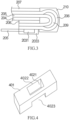
- Fig. 3 is a bending state of the OLED display panel. Reference numbers are identical to those in Fig. 2 , and the specific structure is not repeated again.
- the reinforcing plate 401 includes a body thereof.
- a chamber 4021 is formed in a bottom portion of the reinforcing plate 401.
- the chamber 4021 is used to evade a position of the driving chip and is able to protect the driving chip simultaneously, so as to avoid a risk of being scratched easily due to the driving chip protruding from the back portion of the OLED display panel after the bending.
- a first opening 4022 is disposed in a top portion of the reinforcing plate 401.
- the chamber 4021 is extended upwardly to the top portion of the reinforcing plate 401 and combined with the first opening 4022.
- a top surface of the driving chip is parallel and aligned to a plane at which the first opening 4022 located, such that a thickness of the reinforcing plate 401 can be reduced. Therefore, a thickness of the product is not increased by the disposing of the fixing plate.
- a second opening 4023 is disposed in the reinforcing plate 401 towards an end of the driving chip connected with the flexible circuit board, and a top portion of the second opening 4023 is slightly higher than the flexible circuit board.
- An end of the flexible circuit board is extended from the second opening 4023 into the chamber 4021 for connecting with pins of the driving chip.
- a plurality of adhesive grooves are disposed in the bottom portion of the reinforcing plate 401.
- a glue is not pushed out of an adhesive surface of the bottom portion of the reinforcing plate 401, but is gathered in the adhesive grooves of the bottom portion of the reinforcing plate 401, so as to eliminate the trouble of cleaning the residual glue.
- the adhesive grooves increase an adhesive area between the bottom portion of the reinforcing plate and the flexible substrate, and the fixation of the reinforcing plate 401 is further enhanced.
- an OLED display device comprising: an OLED display panel, defined as: a display region comprising: a first protective layer, a flexible substrate, a substrate wiring layer and a display element layer which are sequentially stacked and disposed, wherein the flexible substrate and the substrate wiring layer are extended toward a side of the display region; a bending region being a first extending portion of the flexible substrate and the substrate wiring layer; and a driving bonding region being a second extending portion of the flexible substrate and the substrate wiring layer, wherein the second extending portion is located outside the first extending portion; wherein the driving bonding region comprises: a driving chip disposed on a surface of the substrate wiring layer and configured to input a requiring voltage to each of pixels; a flexible circuit board configured to achieve a connection between the driving chip and a motherboard; and a reinforcing plate adhesive to and covering a surface of the substrate wiring layer of the driving bonding region, wherein a chamber is formed in a bottom portion of the reinforcing plate, and the driving chip is located in
- the operation principle of the OLED display device of the present preferred embodiment is identical to that of the OLED display panel of the above preferred embodiment. Specifically, the operation principle of the OLED display panel of the preferred embodiment described above can be referred thereto, and here is not repeated again.
- the beneficial effects are that: in comparison with a conventional OLED display panel, the OLED display panel of the present disclosure improves toughness of parts of flexible substrates by disposing a reinforcing plate in a driving region, so as to achieve easy bending; reducing an amount of deformation of the flexible substrates; and improving a fitting accuracy and inducing a protection on a driving chip. Therefore, the technical problems in the conventional OLED display panels, which a poor bending accuracy of parts of panels is induced by a material problem of the flexible substrates upon bending and the driving chip is not protected after the bending of parts of the panels, so as to affect the display effect, are solved.
Landscapes
- Engineering & Computer Science (AREA)
- Microelectronics & Electronic Packaging (AREA)
- Physics & Mathematics (AREA)
- Optics & Photonics (AREA)
- Electroluminescent Light Sources (AREA)
- Devices For Indicating Variable Information By Combining Individual Elements (AREA)
Claims (6)
- Eine OLED-Anzeigetafel, die folgende Merkmale aufweist:eine Anzeigeregion (101) mit: einer ersten Schutzschicht (204), einem flexiblen Substrat (205), einer Substratverdrahtungsschicht (206) und einer Anzeigeelementschicht (207), die der Reihe nach gestapelt und angeordnet sind, wobei das flexible Substrat (205) und die Substratverdrahtungsschicht (206) in Richtung einer Seite der Anzeigeregion (101) erweitert sind;eine Biegeregion (102), die ein erster Erweiterungsabschnitt des flexiblen Substrats (205) und der Substratverdrahtungsschicht (206) ist; undeine Treiberbindungsregion (203), die ein zweiter Erweiterungsabschnitt des flexiblen Substrats (205) und der Substratverdrahtungsschicht (206) ist, wobei sich der zweite Erweiterungsabschnitt außerhalb des ersten Erweiterungsabschnitts befindet; wobei die Treiberbindungsregion (203) folgende Merkmale aufweist:einen Treiberchip (1031), der an einer Oberfläche der Substratverdrahtungsschicht (206) angeordnet und dazu ausgebildet ist, eine Spannung an jedes Pixel einzugeben;eine flexible Schaltungsplatine (1032), die dazu ausgebildet ist, eine Verbindung zwischen dem Treiberchip (1031) und einer Hauptplatine zu erzielen; undeine Verstärkungsplatte (1033), die an der Oberfläche der Substratverdrahtungsschicht (206) der Treiberbindungsregion (203) angeordnet ist und die Oberfläche der Substratverdrahtungsschicht (206) der Treiberbindungsregion (203) bedeckt, wobei eine Kammer (4021) in einem Bodenabschnitt der Verstärkungsplatte (1033) gebildet ist und der Treiberchip (1031) sich in der Kammer (4021) befindet;dadurch gekennzeichnet, dass eine zweite Öffnung (4023) in einer Seite der Kammer (4021) der Verstärkungsplatte (1033) angeordnet ist, die zweite Öffnung (4023) in Richtung des Treiberchips (1031) zeigt und mit einem Ende der flexiblen Schaltungsplatine (1032) verbunden ist und ein oberer Abschnitt der zweiten Öffnung (4023) etwas höher ist als eine obere Oberfläche der flexiblen Schaltungsplatine (1032).
- Die OLED-Anzeigetafel gemäß Anspruch 1, bei der die Verstärkungsplatte (1033) an der Oberfläche der Substratverdrahtungsschicht (206) der Treiberbindungsregion (203) angeordnet ist und eine Mehrzahl von Haftrillen in dem Bodenabschnitt angeordnet ist.
- Die OLED-Anzeigetafel gemäß einem der Ansprüche 1 und 2, bei der eine zweite Schutzschicht (209) zwischen dem flexiblen Substrat (205) und der Substratverdrahtungsschicht (206) der Biegeregion (102) hergestellt ist; und eine dritte Schutzschicht (210) an einer oberen Oberfläche der Substratverdrahtungsschicht (206) hergestellt ist.
- Die OLED-Anzeigetafel gemäß einem der Ansprüche 1-3, bei der die Verstärkungsplatte (1033) einstückig mit einem starren PET-Material geformt ist.
- Die OLED-Anzeigetafel gemäß einem der Ansprüche 1-4, bei der eine erste Öffnung (4022) in einem oberen Abschnitt der Kammer (4021) der Verstärkungsplatte (1033) angeordnet ist, wobei eine Ebene, an der sich der obere Abschnitt der Kammer (4021) befindet, parallel zu und ausgerichtet mit einer oberen Oberfläche des Treiberchips (1031) ist.
- Eine OLED-Anzeigevorrichtung, die eine OLED-Anzeigetafel gemäß einem der Ansprüche 1-5 aufweist.
Applications Claiming Priority (2)
| Application Number | Priority Date | Filing Date | Title |
|---|---|---|---|
| CN201710174784.3A CN106847871B (zh) | 2017-03-22 | 2017-03-22 | Oled显示面板及其显示装置 |
| PCT/CN2017/080961 WO2018170979A1 (zh) | 2017-03-22 | 2017-04-18 | Oled显示面板及其显示装置 |
Publications (3)
| Publication Number | Publication Date |
|---|---|
| EP3605509A1 EP3605509A1 (de) | 2020-02-05 |
| EP3605509A4 EP3605509A4 (de) | 2020-12-23 |
| EP3605509B1 true EP3605509B1 (de) | 2023-06-21 |
Family
ID=59130212
Family Applications (1)
| Application Number | Title | Priority Date | Filing Date |
|---|---|---|---|
| EP17902168.8A Active EP3605509B1 (de) | 2017-03-22 | 2017-04-18 | Oled-anzeigetafel und anzeigevorrichtung |
Country Status (5)
| Country | Link |
|---|---|
| US (1) | US10381594B2 (de) |
| EP (1) | EP3605509B1 (de) |
| JP (1) | JP6824419B2 (de) |
| CN (1) | CN106847871B (de) |
| WO (1) | WO2018170979A1 (de) |
Families Citing this family (41)
| Publication number | Priority date | Publication date | Assignee | Title |
|---|---|---|---|---|
| JP2018205486A (ja) * | 2017-06-02 | 2018-12-27 | 株式会社ジャパンディスプレイ | 表示装置および表示装置の製造方法 |
| CN107564416B (zh) * | 2017-09-15 | 2019-08-30 | 上海天马微电子有限公司 | 一种显示面板及显示装置 |
| US10707289B2 (en) | 2018-02-08 | 2020-07-07 | Wuhan China Star Optoelectronics Semiconductor Display Technology Co., Ltd. | Flexible display panel and flexible display |
| CN108389876A (zh) * | 2018-02-08 | 2018-08-10 | 武汉华星光电半导体显示技术有限公司 | 一种柔性显示面板及柔性显示器 |
| CN111788516A (zh) * | 2018-03-16 | 2020-10-16 | 深圳市柔宇科技股份有限公司 | Cof载带及其加工方法、cof载带加工设备 |
| CN108594549B (zh) * | 2018-04-24 | 2020-12-22 | 武汉华星光电技术有限公司 | 面板驱动架构、覆晶柔性薄膜及覆晶柔性薄膜补强方法 |
| CN112889144A (zh) * | 2018-10-22 | 2021-06-01 | 深圳市柔宇科技股份有限公司 | 柔性基材、柔性面板及电子设备 |
| CN109461381B (zh) * | 2018-11-30 | 2021-03-23 | 云谷(固安)科技有限公司 | 一种显示面板、显示装置及显示面板的制作方法 |
| CN109637382A (zh) * | 2018-12-12 | 2019-04-16 | 武汉华星光电半导体显示技术有限公司 | 显示面板及显示装置 |
| CN109640511B (zh) * | 2018-12-14 | 2020-09-08 | 武汉华星光电半导体显示技术有限公司 | 柔性电路板及其制作方法与oled显示装置 |
| CN113169215A (zh) * | 2018-12-19 | 2021-07-23 | 深圳市柔宇科技股份有限公司 | 柔性面板及柔性面板制作方法 |
| WO2020124417A1 (zh) * | 2018-12-19 | 2020-06-25 | 深圳市柔宇科技有限公司 | 柔性面板及柔性面板制作方法 |
| CN109817101B (zh) * | 2019-03-25 | 2020-01-31 | 云谷(固安)科技有限公司 | 一种柔性显示模组和柔性显示屏 |
| CN109976009B (zh) * | 2019-04-15 | 2024-04-09 | 武汉华星光电技术有限公司 | 显示面板、芯片及柔性电路板 |
| CN110164874B (zh) * | 2019-06-04 | 2021-06-22 | 上海天马微电子有限公司 | 柔性显示模组、显示装置及柔性显示模组的制作方法 |
| CN110224081B (zh) * | 2019-06-24 | 2022-04-12 | 京东方科技集团股份有限公司 | 一种显示模组和显示设备 |
| CN110610904A (zh) | 2019-08-29 | 2019-12-24 | 武汉华星光电半导体显示技术有限公司 | 显示面板及其制作方法 |
| US11129284B2 (en) * | 2019-09-16 | 2021-09-21 | Apple Inc. | Display system and rigid flex PCB with flip chip bonded inside cavity |
| CN110570753B (zh) * | 2019-09-17 | 2021-08-03 | 京东方科技集团股份有限公司 | 一种显示装置及其组装方法 |
| KR20210035382A (ko) | 2019-09-23 | 2021-04-01 | 삼성디스플레이 주식회사 | 표시 장치 및 캐리어 패널 |
| CN110797352B (zh) * | 2019-11-08 | 2022-10-28 | 京东方科技集团股份有限公司 | 显示面板及其制作方法、显示装置 |
| CN110674797B (zh) * | 2019-11-11 | 2025-10-03 | 昆山丘钛生物识别科技有限公司 | 光学指纹模组和移动终端 |
| CN113644181B (zh) * | 2020-05-11 | 2024-04-16 | 京东方科技集团股份有限公司 | 发光基板及其制造方法、显示装置 |
| CN111554202B (zh) * | 2020-05-27 | 2022-08-09 | 上海中航光电子有限公司 | 一种显示面板和显示装置 |
| CN111833742B (zh) * | 2020-06-30 | 2022-07-05 | 合肥维信诺科技有限公司 | 一种显示装置 |
| KR102743166B1 (ko) | 2020-07-15 | 2024-12-18 | 삼성디스플레이 주식회사 | 전자 장치 |
| US11889647B2 (en) | 2020-08-19 | 2024-01-30 | Apple Inc. | Display panel bend reinforcement |
| CN112002257B (zh) * | 2020-09-25 | 2025-03-21 | 京东方科技集团股份有限公司 | 显示模组和显示装置 |
| CN112310139B (zh) * | 2020-10-19 | 2023-04-07 | 深圳市华星光电半导体显示技术有限公司 | 显示基板及其制备方法、显示装置 |
| CN112599021B (zh) * | 2021-01-06 | 2022-08-05 | 武汉华星光电半导体显示技术有限公司 | 显示装置 |
| CN113053246A (zh) | 2021-03-12 | 2021-06-29 | 京东方科技集团股份有限公司 | 一种显示面板、显示装置 |
| CN113192420A (zh) * | 2021-04-09 | 2021-07-30 | 武汉华星光电半导体显示技术有限公司 | 柔性显示面板及显示装置 |
| CN113270039B (zh) * | 2021-05-20 | 2022-07-19 | 昆山国显光电有限公司 | 显示模组 |
| WO2022252094A1 (zh) * | 2021-05-31 | 2022-12-08 | 京东方科技集团股份有限公司 | 显示基板及其制作方法、显示装置 |
| CN113436530B (zh) * | 2021-06-16 | 2022-05-03 | 武汉华星光电半导体显示技术有限公司 | 显示模组及其制作方法、显示装置 |
| CN113471258B (zh) * | 2021-06-22 | 2022-04-08 | 武汉华星光电技术有限公司 | 显示装置 |
| CN113707014B (zh) * | 2021-08-18 | 2022-07-12 | 武汉华星光电半导体显示技术有限公司 | 一种显示装置 |
| CN116978898A (zh) * | 2022-04-15 | 2023-10-31 | 华为技术有限公司 | 显示模组、电子设备、显示模组的制备方法 |
| CN115798325A (zh) * | 2022-11-11 | 2023-03-14 | 合肥维信诺科技有限公司 | 显示模组和绝缘胶带 |
| WO2025097332A1 (zh) * | 2023-11-08 | 2025-05-15 | 上海显耀显示科技有限公司 | 微型显示面板 |
| CN121053857A (zh) * | 2024-05-31 | 2025-12-02 | 京东方科技集团股份有限公司 | 显示面板、显示模组及其制作方法、面板电路板 |
Citations (1)
| Publication number | Priority date | Publication date | Assignee | Title |
|---|---|---|---|---|
| US20140177147A1 (en) * | 2012-12-26 | 2014-06-26 | Mitsubishi Electric Corporation | Display device and method of manufacturing the same |
Family Cites Families (26)
| Publication number | Priority date | Publication date | Assignee | Title |
|---|---|---|---|---|
| JPH0358679U (de) * | 1989-10-13 | 1991-06-07 | ||
| JPH05144875A (ja) * | 1991-11-18 | 1993-06-11 | Sharp Corp | 配線基板の実装方法 |
| JPH08213072A (ja) * | 1995-02-06 | 1996-08-20 | Casio Comput Co Ltd | 電子部品の実装構造 |
| JP2005134637A (ja) * | 2003-10-30 | 2005-05-26 | Optrex Corp | 液晶表示装置 |
| JP2008159873A (ja) * | 2006-12-25 | 2008-07-10 | Epson Imaging Devices Corp | フレキシブルプリント配線基板およびその製造方法、電気光学装置および電子機器 |
| KR100942554B1 (ko) * | 2008-02-21 | 2010-02-12 | 삼성모바일디스플레이주식회사 | 평판표시장치 |
| TW201007894A (en) * | 2008-08-07 | 2010-02-16 | Univ Ishou | Packaging structure of driver IC used in flat panel display and flexible carrier board used for packaging driver IC |
| JP5008767B2 (ja) * | 2008-09-29 | 2012-08-22 | シャープ株式会社 | 基板モジュールおよびその製造方法 |
| CN201967253U (zh) * | 2011-03-10 | 2011-09-07 | 福建火炬电子科技股份有限公司 | 一种用于连接器的滤波电路板 |
| JP2013020133A (ja) * | 2011-07-12 | 2013-01-31 | Fujitsu Mobile Communications Ltd | 液晶表示装置及び電子機器 |
| KR101942918B1 (ko) * | 2012-05-03 | 2019-01-28 | 삼성전자주식회사 | 칩 온 필름 패키지 및 이를 포함하는 장치 어셈블리 |
| KR102017158B1 (ko) * | 2013-03-04 | 2019-09-02 | 삼성전자주식회사 | 칩 온 필름 패키지 및 이를 갖는 표시 장치 |
| KR102081650B1 (ko) * | 2013-04-10 | 2020-02-26 | 엘지디스플레이 주식회사 | 플렉서블 디스플레이 장치 및 그 제조 방법 |
| KR102033625B1 (ko) * | 2013-04-10 | 2019-10-17 | 엘지디스플레이 주식회사 | 플렉서블 디스플레이 장치 및 그 제조 방법 |
| KR102089246B1 (ko) * | 2013-07-19 | 2020-03-16 | 엘지디스플레이 주식회사 | 플렉서블 디스플레이 장치 및 플렉서블 디스플레이 장치의 제조방법 |
| KR102305489B1 (ko) * | 2015-01-26 | 2021-09-28 | 삼성디스플레이 주식회사 | 표시 장치 및 그 제조 방법 |
| JP6448391B2 (ja) * | 2015-01-28 | 2019-01-09 | 株式会社ジャパンディスプレイ | 表示モジュール |
| KR102363261B1 (ko) * | 2015-04-16 | 2022-02-16 | 삼성디스플레이 주식회사 | 플렉시블 디스플레이 패널 및 그 제조방법 |
| JP6506653B2 (ja) * | 2015-07-30 | 2019-04-24 | 日本メクトロン株式会社 | 伸縮性配線基板 |
| KR102463838B1 (ko) * | 2015-08-24 | 2022-11-04 | 삼성디스플레이 주식회사 | 가요성 표시 장치와 이의 제조 방법 |
| CN204884440U (zh) * | 2015-08-27 | 2015-12-16 | 京东方科技集团股份有限公司 | 柔性显示面板和柔性显示装置 |
| CN105530755B (zh) * | 2016-02-25 | 2018-01-23 | 广东欧珀移动通信有限公司 | 软硬结合板及移动终端 |
| KR102596956B1 (ko) * | 2016-05-23 | 2023-11-01 | 삼성디스플레이 주식회사 | 표시 장치 |
| KR20180032742A (ko) * | 2016-09-22 | 2018-04-02 | 삼성디스플레이 주식회사 | 플렉시블 디스플레이 패널 및 플렉시블 디스플레이 패널 벤딩 방법 |
| CN106299098B (zh) * | 2016-10-12 | 2018-10-26 | 成都寰宇科芯科技有限责任公司 | Commb-led光源的外引电极的制造方法 |
| CN106383555A (zh) * | 2016-10-20 | 2017-02-08 | 成都京东方光电科技有限公司 | 一种柔性显示面板及其制作方法、显示装置 |
-
2017
- 2017-03-22 CN CN201710174784.3A patent/CN106847871B/zh active Active
- 2017-04-18 US US15/566,714 patent/US10381594B2/en active Active
- 2017-04-18 JP JP2019535317A patent/JP6824419B2/ja active Active
- 2017-04-18 EP EP17902168.8A patent/EP3605509B1/de active Active
- 2017-04-18 WO PCT/CN2017/080961 patent/WO2018170979A1/zh not_active Ceased
Patent Citations (1)
| Publication number | Priority date | Publication date | Assignee | Title |
|---|---|---|---|---|
| US20140177147A1 (en) * | 2012-12-26 | 2014-06-26 | Mitsubishi Electric Corporation | Display device and method of manufacturing the same |
Also Published As
| Publication number | Publication date |
|---|---|
| CN106847871A (zh) | 2017-06-13 |
| US20190036075A1 (en) | 2019-01-31 |
| JP2020503651A (ja) | 2020-01-30 |
| CN106847871B (zh) | 2020-06-16 |
| EP3605509A4 (de) | 2020-12-23 |
| JP6824419B2 (ja) | 2021-02-03 |
| EP3605509A1 (de) | 2020-02-05 |
| US10381594B2 (en) | 2019-08-13 |
| WO2018170979A1 (zh) | 2018-09-27 |
Similar Documents
| Publication | Publication Date | Title |
|---|---|---|
| US10381594B2 (en) | OLED display panel and display device thereof | |
| US9362521B2 (en) | Organic light emitting diode display | |
| EP3244385B1 (de) | Anzeigesubstrat, anzeigetafel und anzeigevorrichtung | |
| US8817223B2 (en) | Flexible display device and fabrication method thereof | |
| KR102035005B1 (ko) | 터치 표시장치 | |
| US10191517B2 (en) | Flexible device | |
| US10172233B2 (en) | Display device and manufacturing method thereof | |
| US20180166037A1 (en) | Display apparatus having a small bezel | |
| US11163185B2 (en) | Display device | |
| US10082897B2 (en) | Double-sided touch panel display device and manufacturing method | |
| KR20170015805A (ko) | 플렉서블 표시 장치 및 그의 제조 방법 | |
| TWI691756B (zh) | 背蓋及包含其之顯示器 | |
| KR102852919B1 (ko) | 디스플레이 모듈 및 디스플레이 장치 | |
| US20210011566A1 (en) | Display module and electronic equipment | |
| CN113284423A (zh) | 一种柔性显示面板及显示装置 | |
| US20210304641A1 (en) | Large rollable display device and method for manufacturing same | |
| US20250328041A1 (en) | Electronic device | |
| KR20180058283A (ko) | 플렉서블 표시장치 | |
| WO2022241857A1 (zh) | 一种自容式触控显示面板及显示装置 | |
| US10950670B2 (en) | Display panel | |
| US10203552B2 (en) | Rubber frame and manufacturing method thereof, backlight module, and display device and assembling method thereof | |
| US9007778B2 (en) | Signal wiring of touch panel | |
| US20160225830A1 (en) | Organic light emitting diode display | |
| KR102901656B1 (ko) | 표시장치 | |
| KR20180028202A (ko) | 곡면형 디스플레이장치의 제조방법 |
Legal Events
| Date | Code | Title | Description |
|---|---|---|---|
| STAA | Information on the status of an ep patent application or granted ep patent |
Free format text: STATUS: THE INTERNATIONAL PUBLICATION HAS BEEN MADE |
|
| PUAI | Public reference made under article 153(3) epc to a published international application that has entered the european phase |
Free format text: ORIGINAL CODE: 0009012 |
|
| STAA | Information on the status of an ep patent application or granted ep patent |
Free format text: STATUS: REQUEST FOR EXAMINATION WAS MADE |
|
| 17P | Request for examination filed |
Effective date: 20191022 |
|
| AK | Designated contracting states |
Kind code of ref document: A1 Designated state(s): AL AT BE BG CH CY CZ DE DK EE ES FI FR GB GR HR HU IE IS IT LI LT LU LV MC MK MT NL NO PL PT RO RS SE SI SK SM TR |
|
| AX | Request for extension of the european patent |
Extension state: BA ME |
|
| DAV | Request for validation of the european patent (deleted) | ||
| DAX | Request for extension of the european patent (deleted) | ||
| A4 | Supplementary search report drawn up and despatched |
Effective date: 20201120 |
|
| RIC1 | Information provided on ipc code assigned before grant |
Ipc: H01L 27/32 20060101ALI20201116BHEP Ipc: H01L 51/54 20060101ALI20201116BHEP Ipc: G09F 9/00 20060101AFI20201116BHEP Ipc: H01L 51/52 20060101ALI20201116BHEP |
|
| REG | Reference to a national code |
Ref country code: DE Ref legal event code: R079 Free format text: PREVIOUS MAIN CLASS: G09F0009000000 Ipc: H10K0050844000 Ref country code: DE Ref legal event code: R079 Ref document number: 602017070554 Country of ref document: DE Free format text: PREVIOUS MAIN CLASS: G09F0009000000 Ipc: H10K0050844000 |
|
| GRAP | Despatch of communication of intention to grant a patent |
Free format text: ORIGINAL CODE: EPIDOSNIGR1 |
|
| STAA | Information on the status of an ep patent application or granted ep patent |
Free format text: STATUS: GRANT OF PATENT IS INTENDED |
|
| RIC1 | Information provided on ipc code assigned before grant |
Ipc: H10K 59/131 20230101ALI20230111BHEP Ipc: H10K 77/10 20230101ALI20230111BHEP Ipc: H10K 50/844 20230101AFI20230111BHEP |
|
| INTG | Intention to grant announced |
Effective date: 20230131 |
|
| GRAS | Grant fee paid |
Free format text: ORIGINAL CODE: EPIDOSNIGR3 |
|
| GRAA | (expected) grant |
Free format text: ORIGINAL CODE: 0009210 |
|
| STAA | Information on the status of an ep patent application or granted ep patent |
Free format text: STATUS: THE PATENT HAS BEEN GRANTED |
|
| AK | Designated contracting states |
Kind code of ref document: B1 Designated state(s): AL AT BE BG CH CY CZ DE DK EE ES FI FR GB GR HR HU IE IS IT LI LT LU LV MC MK MT NL NO PL PT RO RS SE SI SK SM TR |
|
| REG | Reference to a national code |
Ref country code: CH Ref legal event code: EP |
|
| P01 | Opt-out of the competence of the unified patent court (upc) registered |
Effective date: 20230530 |
|
| REG | Reference to a national code |
Ref country code: DE Ref legal event code: R096 Ref document number: 602017070554 Country of ref document: DE |
|
| REG | Reference to a national code |
Ref country code: AT Ref legal event code: REF Ref document number: 1581859 Country of ref document: AT Kind code of ref document: T Effective date: 20230715 |
|
| REG | Reference to a national code |
Ref country code: IE Ref legal event code: FG4D |
|
| REG | Reference to a national code |
Ref country code: LT Ref legal event code: MG9D |
|
| REG | Reference to a national code |
Ref country code: NL Ref legal event code: MP Effective date: 20230621 |
|
| PG25 | Lapsed in a contracting state [announced via postgrant information from national office to epo] |
Ref country code: SE Free format text: LAPSE BECAUSE OF FAILURE TO SUBMIT A TRANSLATION OF THE DESCRIPTION OR TO PAY THE FEE WITHIN THE PRESCRIBED TIME-LIMIT Effective date: 20230621 Ref country code: NO Free format text: LAPSE BECAUSE OF FAILURE TO SUBMIT A TRANSLATION OF THE DESCRIPTION OR TO PAY THE FEE WITHIN THE PRESCRIBED TIME-LIMIT Effective date: 20230921 |
|
| REG | Reference to a national code |
Ref country code: AT Ref legal event code: MK05 Ref document number: 1581859 Country of ref document: AT Kind code of ref document: T Effective date: 20230621 |
|
| PG25 | Lapsed in a contracting state [announced via postgrant information from national office to epo] |
Ref country code: RS Free format text: LAPSE BECAUSE OF FAILURE TO SUBMIT A TRANSLATION OF THE DESCRIPTION OR TO PAY THE FEE WITHIN THE PRESCRIBED TIME-LIMIT Effective date: 20230621 Ref country code: NL Free format text: LAPSE BECAUSE OF FAILURE TO SUBMIT A TRANSLATION OF THE DESCRIPTION OR TO PAY THE FEE WITHIN THE PRESCRIBED TIME-LIMIT Effective date: 20230621 Ref country code: LV Free format text: LAPSE BECAUSE OF FAILURE TO SUBMIT A TRANSLATION OF THE DESCRIPTION OR TO PAY THE FEE WITHIN THE PRESCRIBED TIME-LIMIT Effective date: 20230621 Ref country code: LT Free format text: LAPSE BECAUSE OF FAILURE TO SUBMIT A TRANSLATION OF THE DESCRIPTION OR TO PAY THE FEE WITHIN THE PRESCRIBED TIME-LIMIT Effective date: 20230621 Ref country code: HR Free format text: LAPSE BECAUSE OF FAILURE TO SUBMIT A TRANSLATION OF THE DESCRIPTION OR TO PAY THE FEE WITHIN THE PRESCRIBED TIME-LIMIT Effective date: 20230621 Ref country code: GR Free format text: LAPSE BECAUSE OF FAILURE TO SUBMIT A TRANSLATION OF THE DESCRIPTION OR TO PAY THE FEE WITHIN THE PRESCRIBED TIME-LIMIT Effective date: 20230922 |
|
| PG25 | Lapsed in a contracting state [announced via postgrant information from national office to epo] |
Ref country code: FI Free format text: LAPSE BECAUSE OF FAILURE TO SUBMIT A TRANSLATION OF THE DESCRIPTION OR TO PAY THE FEE WITHIN THE PRESCRIBED TIME-LIMIT Effective date: 20230621 |
|
| PG25 | Lapsed in a contracting state [announced via postgrant information from national office to epo] |
Ref country code: SK Free format text: LAPSE BECAUSE OF FAILURE TO SUBMIT A TRANSLATION OF THE DESCRIPTION OR TO PAY THE FEE WITHIN THE PRESCRIBED TIME-LIMIT Effective date: 20230621 |
|
| PG25 | Lapsed in a contracting state [announced via postgrant information from national office to epo] |
Ref country code: ES Free format text: LAPSE BECAUSE OF FAILURE TO SUBMIT A TRANSLATION OF THE DESCRIPTION OR TO PAY THE FEE WITHIN THE PRESCRIBED TIME-LIMIT Effective date: 20230621 |
|
| PG25 | Lapsed in a contracting state [announced via postgrant information from national office to epo] |
Ref country code: IS Free format text: LAPSE BECAUSE OF FAILURE TO SUBMIT A TRANSLATION OF THE DESCRIPTION OR TO PAY THE FEE WITHIN THE PRESCRIBED TIME-LIMIT Effective date: 20231021 |
|
| PG25 | Lapsed in a contracting state [announced via postgrant information from national office to epo] |
Ref country code: SM Free format text: LAPSE BECAUSE OF FAILURE TO SUBMIT A TRANSLATION OF THE DESCRIPTION OR TO PAY THE FEE WITHIN THE PRESCRIBED TIME-LIMIT Effective date: 20230621 Ref country code: SK Free format text: LAPSE BECAUSE OF FAILURE TO SUBMIT A TRANSLATION OF THE DESCRIPTION OR TO PAY THE FEE WITHIN THE PRESCRIBED TIME-LIMIT Effective date: 20230621 Ref country code: RO Free format text: LAPSE BECAUSE OF FAILURE TO SUBMIT A TRANSLATION OF THE DESCRIPTION OR TO PAY THE FEE WITHIN THE PRESCRIBED TIME-LIMIT Effective date: 20230621 Ref country code: PT Free format text: LAPSE BECAUSE OF FAILURE TO SUBMIT A TRANSLATION OF THE DESCRIPTION OR TO PAY THE FEE WITHIN THE PRESCRIBED TIME-LIMIT Effective date: 20231023 Ref country code: IS Free format text: LAPSE BECAUSE OF FAILURE TO SUBMIT A TRANSLATION OF THE DESCRIPTION OR TO PAY THE FEE WITHIN THE PRESCRIBED TIME-LIMIT Effective date: 20231021 Ref country code: ES Free format text: LAPSE BECAUSE OF FAILURE TO SUBMIT A TRANSLATION OF THE DESCRIPTION OR TO PAY THE FEE WITHIN THE PRESCRIBED TIME-LIMIT Effective date: 20230621 Ref country code: EE Free format text: LAPSE BECAUSE OF FAILURE TO SUBMIT A TRANSLATION OF THE DESCRIPTION OR TO PAY THE FEE WITHIN THE PRESCRIBED TIME-LIMIT Effective date: 20230621 Ref country code: CZ Free format text: LAPSE BECAUSE OF FAILURE TO SUBMIT A TRANSLATION OF THE DESCRIPTION OR TO PAY THE FEE WITHIN THE PRESCRIBED TIME-LIMIT Effective date: 20230621 Ref country code: AT Free format text: LAPSE BECAUSE OF FAILURE TO SUBMIT A TRANSLATION OF THE DESCRIPTION OR TO PAY THE FEE WITHIN THE PRESCRIBED TIME-LIMIT Effective date: 20230621 |
|
| PG25 | Lapsed in a contracting state [announced via postgrant information from national office to epo] |
Ref country code: PL Free format text: LAPSE BECAUSE OF FAILURE TO SUBMIT A TRANSLATION OF THE DESCRIPTION OR TO PAY THE FEE WITHIN THE PRESCRIBED TIME-LIMIT Effective date: 20230621 |
|
| REG | Reference to a national code |
Ref country code: DE Ref legal event code: R097 Ref document number: 602017070554 Country of ref document: DE |
|
| PLBE | No opposition filed within time limit |
Free format text: ORIGINAL CODE: 0009261 |
|
| STAA | Information on the status of an ep patent application or granted ep patent |
Free format text: STATUS: NO OPPOSITION FILED WITHIN TIME LIMIT |
|
| PG25 | Lapsed in a contracting state [announced via postgrant information from national office to epo] |
Ref country code: DK Free format text: LAPSE BECAUSE OF FAILURE TO SUBMIT A TRANSLATION OF THE DESCRIPTION OR TO PAY THE FEE WITHIN THE PRESCRIBED TIME-LIMIT Effective date: 20230621 |
|
| PG25 | Lapsed in a contracting state [announced via postgrant information from national office to epo] |
Ref country code: SI Free format text: LAPSE BECAUSE OF FAILURE TO SUBMIT A TRANSLATION OF THE DESCRIPTION OR TO PAY THE FEE WITHIN THE PRESCRIBED TIME-LIMIT Effective date: 20230621 |
|
| 26N | No opposition filed |
Effective date: 20240322 |
|
| PG25 | Lapsed in a contracting state [announced via postgrant information from national office to epo] |
Ref country code: SI Free format text: LAPSE BECAUSE OF FAILURE TO SUBMIT A TRANSLATION OF THE DESCRIPTION OR TO PAY THE FEE WITHIN THE PRESCRIBED TIME-LIMIT Effective date: 20230621 Ref country code: IT Free format text: LAPSE BECAUSE OF FAILURE TO SUBMIT A TRANSLATION OF THE DESCRIPTION OR TO PAY THE FEE WITHIN THE PRESCRIBED TIME-LIMIT Effective date: 20230621 |
|
| PG25 | Lapsed in a contracting state [announced via postgrant information from national office to epo] |
Ref country code: BG Free format text: LAPSE BECAUSE OF FAILURE TO SUBMIT A TRANSLATION OF THE DESCRIPTION OR TO PAY THE FEE WITHIN THE PRESCRIBED TIME-LIMIT Effective date: 20230621 |
|
| PG25 | Lapsed in a contracting state [announced via postgrant information from national office to epo] |
Ref country code: MC Free format text: LAPSE BECAUSE OF FAILURE TO SUBMIT A TRANSLATION OF THE DESCRIPTION OR TO PAY THE FEE WITHIN THE PRESCRIBED TIME-LIMIT Effective date: 20230621 |
|
| PG25 | Lapsed in a contracting state [announced via postgrant information from national office to epo] |
Ref country code: MC Free format text: LAPSE BECAUSE OF FAILURE TO SUBMIT A TRANSLATION OF THE DESCRIPTION OR TO PAY THE FEE WITHIN THE PRESCRIBED TIME-LIMIT Effective date: 20230621 Ref country code: BG Free format text: LAPSE BECAUSE OF FAILURE TO SUBMIT A TRANSLATION OF THE DESCRIPTION OR TO PAY THE FEE WITHIN THE PRESCRIBED TIME-LIMIT Effective date: 20230621 |
|
| REG | Reference to a national code |
Ref country code: CH Ref legal event code: PL |
|
| PG25 | Lapsed in a contracting state [announced via postgrant information from national office to epo] |
Ref country code: LU Free format text: LAPSE BECAUSE OF NON-PAYMENT OF DUE FEES Effective date: 20240418 |
|
| GBPC | Gb: european patent ceased through non-payment of renewal fee |
Effective date: 20240418 |
|
| REG | Reference to a national code |
Ref country code: BE Ref legal event code: MM Effective date: 20240430 |
|
| PG25 | Lapsed in a contracting state [announced via postgrant information from national office to epo] |
Ref country code: LU Free format text: LAPSE BECAUSE OF NON-PAYMENT OF DUE FEES Effective date: 20240418 |
|
| PG25 | Lapsed in a contracting state [announced via postgrant information from national office to epo] |
Ref country code: BE Free format text: LAPSE BECAUSE OF NON-PAYMENT OF DUE FEES Effective date: 20240430 |
|
| PG25 | Lapsed in a contracting state [announced via postgrant information from national office to epo] |
Ref country code: GB Free format text: LAPSE BECAUSE OF NON-PAYMENT OF DUE FEES Effective date: 20240418 |
|
| PG25 | Lapsed in a contracting state [announced via postgrant information from national office to epo] |
Ref country code: FR Free format text: LAPSE BECAUSE OF NON-PAYMENT OF DUE FEES Effective date: 20240430 |
|
| PG25 | Lapsed in a contracting state [announced via postgrant information from national office to epo] |
Ref country code: GB Free format text: LAPSE BECAUSE OF NON-PAYMENT OF DUE FEES Effective date: 20240418 Ref country code: FR Free format text: LAPSE BECAUSE OF NON-PAYMENT OF DUE FEES Effective date: 20240430 Ref country code: BE Free format text: LAPSE BECAUSE OF NON-PAYMENT OF DUE FEES Effective date: 20240430 Ref country code: CH Free format text: LAPSE BECAUSE OF NON-PAYMENT OF DUE FEES Effective date: 20240430 |
|
| PG25 | Lapsed in a contracting state [announced via postgrant information from national office to epo] |
Ref country code: IE Free format text: LAPSE BECAUSE OF NON-PAYMENT OF DUE FEES Effective date: 20240418 |
|
| PGFP | Annual fee paid to national office [announced via postgrant information from national office to epo] |
Ref country code: DE Payment date: 20250422 Year of fee payment: 9 |
|
| PG25 | Lapsed in a contracting state [announced via postgrant information from national office to epo] |
Ref country code: CY Free format text: LAPSE BECAUSE OF FAILURE TO SUBMIT A TRANSLATION OF THE DESCRIPTION OR TO PAY THE FEE WITHIN THE PRESCRIBED TIME-LIMIT; INVALID AB INITIO Effective date: 20170418 |
|
| PG25 | Lapsed in a contracting state [announced via postgrant information from national office to epo] |
Ref country code: HU Free format text: LAPSE BECAUSE OF FAILURE TO SUBMIT A TRANSLATION OF THE DESCRIPTION OR TO PAY THE FEE WITHIN THE PRESCRIBED TIME-LIMIT; INVALID AB INITIO Effective date: 20170418 |