EP3573108A1 - Procédé de fabrication d'un dispositif semi-conducteur - Google Patents
Procédé de fabrication d'un dispositif semi-conducteur Download PDFInfo
- Publication number
- EP3573108A1 EP3573108A1 EP19185984.2A EP19185984A EP3573108A1 EP 3573108 A1 EP3573108 A1 EP 3573108A1 EP 19185984 A EP19185984 A EP 19185984A EP 3573108 A1 EP3573108 A1 EP 3573108A1
- Authority
- EP
- European Patent Office
- Prior art keywords
- layer
- oxide semiconductor
- thin film
- semiconductor layer
- film transistor
- Prior art date
- Legal status (The legal status is an assumption and is not a legal conclusion. Google has not performed a legal analysis and makes no representation as to the accuracy of the status listed.)
- Withdrawn
Links
- 239000004065 semiconductor Substances 0.000 title claims abstract description 496
- 238000000034 method Methods 0.000 title description 101
- 238000004519 manufacturing process Methods 0.000 title description 47
- 230000015572 biosynthetic process Effects 0.000 claims abstract description 72
- 229910052739 hydrogen Inorganic materials 0.000 claims abstract description 23
- 239000001257 hydrogen Substances 0.000 claims abstract description 20
- UFHFLCQGNIYNRP-UHFFFAOYSA-N Hydrogen Chemical compound [H][H] UFHFLCQGNIYNRP-UHFFFAOYSA-N 0.000 claims abstract description 15
- 239000013078 crystal Substances 0.000 claims description 34
- 239000011701 zinc Substances 0.000 claims description 8
- 229910052738 indium Inorganic materials 0.000 claims description 5
- 238000001004 secondary ion mass spectrometry Methods 0.000 claims description 3
- 229910052725 zinc Inorganic materials 0.000 claims description 3
- APFVFJFRJDLVQX-UHFFFAOYSA-N indium atom Chemical compound [In] APFVFJFRJDLVQX-UHFFFAOYSA-N 0.000 claims description 2
- HCHKCACWOHOZIP-UHFFFAOYSA-N Zinc Chemical compound [Zn] HCHKCACWOHOZIP-UHFFFAOYSA-N 0.000 claims 1
- 239000010410 layer Substances 0.000 description 771
- 239000010408 film Substances 0.000 description 353
- 239000010409 thin film Substances 0.000 description 296
- 238000010438 heat treatment Methods 0.000 description 161
- 239000000758 substrate Substances 0.000 description 155
- 230000002829 reductive effect Effects 0.000 description 81
- 239000012298 atmosphere Substances 0.000 description 66
- 239000000463 material Substances 0.000 description 60
- 238000012360 testing method Methods 0.000 description 60
- 239000004973 liquid crystal related substance Substances 0.000 description 52
- 229910052760 oxygen Inorganic materials 0.000 description 50
- 238000004544 sputter deposition Methods 0.000 description 49
- 239000001301 oxygen Substances 0.000 description 47
- IJGRMHOSHXDMSA-UHFFFAOYSA-N Atomic nitrogen Chemical compound N#N IJGRMHOSHXDMSA-UHFFFAOYSA-N 0.000 description 46
- QVGXLLKOCUKJST-UHFFFAOYSA-N atomic oxygen Chemical compound [O] QVGXLLKOCUKJST-UHFFFAOYSA-N 0.000 description 46
- 239000007789 gas Substances 0.000 description 45
- XKRFYHLGVUSROY-UHFFFAOYSA-N Argon Chemical compound [Ar] XKRFYHLGVUSROY-UHFFFAOYSA-N 0.000 description 44
- 239000012535 impurity Substances 0.000 description 41
- 229910007541 Zn O Inorganic materials 0.000 description 40
- 239000012299 nitrogen atmosphere Substances 0.000 description 38
- 230000006870 function Effects 0.000 description 35
- 230000001681 protective effect Effects 0.000 description 31
- 238000006356 dehydrogenation reaction Methods 0.000 description 30
- VYPSYNLAJGMNEJ-UHFFFAOYSA-N Silicium dioxide Chemical compound O=[Si]=O VYPSYNLAJGMNEJ-UHFFFAOYSA-N 0.000 description 29
- 230000018044 dehydration Effects 0.000 description 29
- 238000006297 dehydration reaction Methods 0.000 description 29
- 229910052814 silicon oxide Inorganic materials 0.000 description 29
- 238000010583 slow cooling Methods 0.000 description 28
- 239000011261 inert gas Substances 0.000 description 26
- 239000002245 particle Substances 0.000 description 26
- 239000000956 alloy Substances 0.000 description 23
- 229910052786 argon Inorganic materials 0.000 description 23
- 238000005530 etching Methods 0.000 description 23
- 229910052757 nitrogen Inorganic materials 0.000 description 23
- 229910052782 aluminium Inorganic materials 0.000 description 22
- 229910045601 alloy Inorganic materials 0.000 description 21
- XLOMVQKBTHCTTD-UHFFFAOYSA-N Zinc monoxide Chemical compound [Zn]=O XLOMVQKBTHCTTD-UHFFFAOYSA-N 0.000 description 20
- 239000003990 capacitor Substances 0.000 description 20
- 229910052581 Si3N4 Inorganic materials 0.000 description 19
- 239000011159 matrix material Substances 0.000 description 19
- HQVNEWCFYHHQES-UHFFFAOYSA-N silicon nitride Chemical compound N12[Si]34N5[Si]62N3[Si]51N64 HQVNEWCFYHHQES-UHFFFAOYSA-N 0.000 description 19
- 239000010936 titanium Substances 0.000 description 19
- 238000005259 measurement Methods 0.000 description 18
- 239000003094 microcapsule Substances 0.000 description 18
- 239000000123 paper Substances 0.000 description 17
- 229910052719 titanium Inorganic materials 0.000 description 17
- XAGFODPZIPBFFR-UHFFFAOYSA-N aluminium Chemical compound [Al] XAGFODPZIPBFFR-UHFFFAOYSA-N 0.000 description 16
- 229920005989 resin Polymers 0.000 description 16
- 239000011347 resin Substances 0.000 description 16
- 230000005684 electric field Effects 0.000 description 15
- 238000000206 photolithography Methods 0.000 description 15
- 239000011241 protective layer Substances 0.000 description 15
- 239000001307 helium Substances 0.000 description 14
- 229910052734 helium Inorganic materials 0.000 description 14
- SWQJXJOGLNCZEY-UHFFFAOYSA-N helium atom Chemical compound [He] SWQJXJOGLNCZEY-UHFFFAOYSA-N 0.000 description 14
- 229910052751 metal Inorganic materials 0.000 description 14
- 229910052750 molybdenum Inorganic materials 0.000 description 14
- XUIMIQQOPSSXEZ-UHFFFAOYSA-N Silicon Chemical compound [Si] XUIMIQQOPSSXEZ-UHFFFAOYSA-N 0.000 description 13
- 125000004429 atom Chemical group 0.000 description 13
- 230000008569 process Effects 0.000 description 13
- 229910052710 silicon Inorganic materials 0.000 description 13
- 239000010703 silicon Substances 0.000 description 13
- RTAQQCXQSZGOHL-UHFFFAOYSA-N Titanium Chemical compound [Ti] RTAQQCXQSZGOHL-UHFFFAOYSA-N 0.000 description 12
- 239000011521 glass Substances 0.000 description 12
- 239000002184 metal Substances 0.000 description 12
- 239000000565 sealant Substances 0.000 description 12
- 239000002356 single layer Substances 0.000 description 12
- 229910052721 tungsten Inorganic materials 0.000 description 12
- 239000011651 chromium Substances 0.000 description 11
- 239000004020 conductor Substances 0.000 description 11
- 239000011787 zinc oxide Substances 0.000 description 11
- ZOKXTWBITQBERF-UHFFFAOYSA-N Molybdenum Chemical compound [Mo] ZOKXTWBITQBERF-UHFFFAOYSA-N 0.000 description 10
- 229910003437 indium oxide Inorganic materials 0.000 description 10
- PJXISJQVUVHSOJ-UHFFFAOYSA-N indium(iii) oxide Chemical compound [O-2].[O-2].[O-2].[In+3].[In+3] PJXISJQVUVHSOJ-UHFFFAOYSA-N 0.000 description 10
- 239000011733 molybdenum Substances 0.000 description 10
- 229910052754 neon Inorganic materials 0.000 description 10
- GKAOGPIIYCISHV-UHFFFAOYSA-N neon atom Chemical compound [Ne] GKAOGPIIYCISHV-UHFFFAOYSA-N 0.000 description 10
- QTBSBXVTEAMEQO-UHFFFAOYSA-N Acetic acid Chemical compound CC(O)=O QTBSBXVTEAMEQO-UHFFFAOYSA-N 0.000 description 9
- 229910052804 chromium Inorganic materials 0.000 description 9
- 229910052715 tantalum Inorganic materials 0.000 description 9
- 238000000151 deposition Methods 0.000 description 8
- 229910052733 gallium Inorganic materials 0.000 description 8
- 239000000203 mixture Substances 0.000 description 8
- 238000001039 wet etching Methods 0.000 description 8
- 238000004040 coloring Methods 0.000 description 7
- 238000004891 communication Methods 0.000 description 7
- 230000008021 deposition Effects 0.000 description 7
- 238000007667 floating Methods 0.000 description 7
- 238000003780 insertion Methods 0.000 description 7
- 230000037431 insertion Effects 0.000 description 7
- 239000007788 liquid Substances 0.000 description 7
- 239000010937 tungsten Substances 0.000 description 7
- NBIIXXVUZAFLBC-UHFFFAOYSA-N Phosphoric acid Chemical compound OP(O)(O)=O NBIIXXVUZAFLBC-UHFFFAOYSA-N 0.000 description 6
- 239000000945 filler Substances 0.000 description 6
- AMGQUBHHOARCQH-UHFFFAOYSA-N indium;oxotin Chemical compound [In].[Sn]=O AMGQUBHHOARCQH-UHFFFAOYSA-N 0.000 description 6
- 230000009467 reduction Effects 0.000 description 6
- 230000003252 repetitive effect Effects 0.000 description 6
- 239000012798 spherical particle Substances 0.000 description 6
- WFKWXMTUELFFGS-UHFFFAOYSA-N tungsten Chemical compound [W] WFKWXMTUELFFGS-UHFFFAOYSA-N 0.000 description 6
- 239000012300 argon atmosphere Substances 0.000 description 5
- 238000001312 dry etching Methods 0.000 description 5
- 230000000694 effects Effects 0.000 description 5
- 230000008030 elimination Effects 0.000 description 5
- 238000003379 elimination reaction Methods 0.000 description 5
- 238000011156 evaluation Methods 0.000 description 5
- -1 hydrogen ions Chemical class 0.000 description 5
- 229910044991 metal oxide Inorganic materials 0.000 description 5
- 150000004706 metal oxides Chemical class 0.000 description 5
- QGLKJKCYBOYXKC-UHFFFAOYSA-N nonaoxidotritungsten Chemical compound O=[W]1(=O)O[W](=O)(=O)O[W](=O)(=O)O1 QGLKJKCYBOYXKC-UHFFFAOYSA-N 0.000 description 5
- 238000005192 partition Methods 0.000 description 5
- 239000000049 pigment Substances 0.000 description 5
- 229920003023 plastic Polymers 0.000 description 5
- 239000004033 plastic Substances 0.000 description 5
- 238000007670 refining Methods 0.000 description 5
- 238000004088 simulation Methods 0.000 description 5
- 229910001930 tungsten oxide Inorganic materials 0.000 description 5
- VYZAMTAEIAYCRO-UHFFFAOYSA-N Chromium Chemical compound [Cr] VYZAMTAEIAYCRO-UHFFFAOYSA-N 0.000 description 4
- 229910052779 Neodymium Inorganic materials 0.000 description 4
- GWEVSGVZZGPLCZ-UHFFFAOYSA-N Titan oxide Chemical compound O=[Ti]=O GWEVSGVZZGPLCZ-UHFFFAOYSA-N 0.000 description 4
- 230000008859 change Effects 0.000 description 4
- 150000001875 compounds Chemical class 0.000 description 4
- 238000001816 cooling Methods 0.000 description 4
- 229910052802 copper Inorganic materials 0.000 description 4
- 239000010949 copper Substances 0.000 description 4
- 238000009792 diffusion process Methods 0.000 description 4
- KPUWHANPEXNPJT-UHFFFAOYSA-N disiloxane Chemical class [SiH3]O[SiH3] KPUWHANPEXNPJT-UHFFFAOYSA-N 0.000 description 4
- 239000000428 dust Substances 0.000 description 4
- 150000002431 hydrogen Chemical class 0.000 description 4
- 230000006872 improvement Effects 0.000 description 4
- 229910052742 iron Inorganic materials 0.000 description 4
- 239000011859 microparticle Substances 0.000 description 4
- 238000000329 molecular dynamics simulation Methods 0.000 description 4
- QEFYFXOXNSNQGX-UHFFFAOYSA-N neodymium atom Chemical compound [Nd] QEFYFXOXNSNQGX-UHFFFAOYSA-N 0.000 description 4
- 229910052759 nickel Inorganic materials 0.000 description 4
- 150000002894 organic compounds Chemical class 0.000 description 4
- 125000004430 oxygen atom Chemical group O* 0.000 description 4
- 238000005268 plasma chemical vapour deposition Methods 0.000 description 4
- 229910052706 scandium Inorganic materials 0.000 description 4
- SIXSYDAISGFNSX-UHFFFAOYSA-N scandium atom Chemical compound [Sc] SIXSYDAISGFNSX-UHFFFAOYSA-N 0.000 description 4
- 239000000243 solution Substances 0.000 description 4
- 239000002904 solvent Substances 0.000 description 4
- 230000003068 static effect Effects 0.000 description 4
- 238000003860 storage Methods 0.000 description 4
- 239000000126 substance Substances 0.000 description 4
- GUVRBAGPIYLISA-UHFFFAOYSA-N tantalum atom Chemical compound [Ta] GUVRBAGPIYLISA-UHFFFAOYSA-N 0.000 description 4
- VZGDMQKNWNREIO-UHFFFAOYSA-N tetrachloromethane Chemical compound ClC(Cl)(Cl)Cl VZGDMQKNWNREIO-UHFFFAOYSA-N 0.000 description 4
- OGIDPMRJRNCKJF-UHFFFAOYSA-N titanium oxide Inorganic materials [Ti]=O OGIDPMRJRNCKJF-UHFFFAOYSA-N 0.000 description 4
- 210000000707 wrist Anatomy 0.000 description 4
- YVTHLONGBIQYBO-UHFFFAOYSA-N zinc indium(3+) oxygen(2-) Chemical compound [O--].[Zn++].[In+3] YVTHLONGBIQYBO-UHFFFAOYSA-N 0.000 description 4
- ZAMOUSCENKQFHK-UHFFFAOYSA-N Chlorine atom Chemical compound [Cl] ZAMOUSCENKQFHK-UHFFFAOYSA-N 0.000 description 3
- XPDWGBQVDMORPB-UHFFFAOYSA-N Fluoroform Chemical compound FC(F)F XPDWGBQVDMORPB-UHFFFAOYSA-N 0.000 description 3
- 230000005355 Hall effect Effects 0.000 description 3
- GRYLNZFGIOXLOG-UHFFFAOYSA-N Nitric acid Chemical compound O[N+]([O-])=O GRYLNZFGIOXLOG-UHFFFAOYSA-N 0.000 description 3
- NRTOMJZYCJJWKI-UHFFFAOYSA-N Titanium nitride Chemical compound [Ti]#N NRTOMJZYCJJWKI-UHFFFAOYSA-N 0.000 description 3
- NIXOWILDQLNWCW-UHFFFAOYSA-N acrylic acid group Chemical group C(C=C)(=O)O NIXOWILDQLNWCW-UHFFFAOYSA-N 0.000 description 3
- 229910000147 aluminium phosphate Inorganic materials 0.000 description 3
- 239000000969 carrier Substances 0.000 description 3
- 239000000460 chlorine Substances 0.000 description 3
- 229910052801 chlorine Inorganic materials 0.000 description 3
- 239000003086 colorant Substances 0.000 description 3
- 238000002425 crystallisation Methods 0.000 description 3
- 230000008025 crystallization Effects 0.000 description 3
- 238000003795 desorption Methods 0.000 description 3
- 238000010586 diagram Methods 0.000 description 3
- 238000009826 distribution Methods 0.000 description 3
- 239000005262 ferroelectric liquid crystals (FLCs) Substances 0.000 description 3
- 230000007246 mechanism Effects 0.000 description 3
- 239000007769 metal material Substances 0.000 description 3
- 229910017604 nitric acid Inorganic materials 0.000 description 3
- 230000003287 optical effect Effects 0.000 description 3
- 229920006267 polyester film Polymers 0.000 description 3
- 229920002620 polyvinyl fluoride Polymers 0.000 description 3
- 230000004044 response Effects 0.000 description 3
- 230000002441 reversible effect Effects 0.000 description 3
- 230000000630 rising effect Effects 0.000 description 3
- 239000007787 solid Substances 0.000 description 3
- TXEYQDLBPFQVAA-UHFFFAOYSA-N tetrafluoromethane Chemical compound FC(F)(F)F TXEYQDLBPFQVAA-UHFFFAOYSA-N 0.000 description 3
- 239000002699 waste material Substances 0.000 description 3
- UWCWUCKPEYNDNV-LBPRGKRZSA-N 2,6-dimethyl-n-[[(2s)-pyrrolidin-2-yl]methyl]aniline Chemical compound CC1=CC=CC(C)=C1NC[C@H]1NCCC1 UWCWUCKPEYNDNV-LBPRGKRZSA-N 0.000 description 2
- QGZKDVFQNNGYKY-UHFFFAOYSA-N Ammonia Chemical compound N QGZKDVFQNNGYKY-UHFFFAOYSA-N 0.000 description 2
- 239000004215 Carbon black (E152) Substances 0.000 description 2
- CURLTUGMZLYLDI-UHFFFAOYSA-N Carbon dioxide Chemical compound O=C=O CURLTUGMZLYLDI-UHFFFAOYSA-N 0.000 description 2
- KZBUYRJDOAKODT-UHFFFAOYSA-N Chlorine Chemical compound ClCl KZBUYRJDOAKODT-UHFFFAOYSA-N 0.000 description 2
- RYGMFSIKBFXOCR-UHFFFAOYSA-N Copper Chemical compound [Cu] RYGMFSIKBFXOCR-UHFFFAOYSA-N 0.000 description 2
- YCKRFDGAMUMZLT-UHFFFAOYSA-N Fluorine atom Chemical compound [F] YCKRFDGAMUMZLT-UHFFFAOYSA-N 0.000 description 2
- GYHNNYVSQQEPJS-UHFFFAOYSA-N Gallium Chemical compound [Ga] GYHNNYVSQQEPJS-UHFFFAOYSA-N 0.000 description 2
- 206010052128 Glare Diseases 0.000 description 2
- VEXZGXHMUGYJMC-UHFFFAOYSA-N Hydrochloric acid Chemical compound Cl VEXZGXHMUGYJMC-UHFFFAOYSA-N 0.000 description 2
- MHAJPDPJQMAIIY-UHFFFAOYSA-N Hydrogen peroxide Chemical compound OO MHAJPDPJQMAIIY-UHFFFAOYSA-N 0.000 description 2
- FYYHWMGAXLPEAU-UHFFFAOYSA-N Magnesium Chemical compound [Mg] FYYHWMGAXLPEAU-UHFFFAOYSA-N 0.000 description 2
- 239000004642 Polyimide Substances 0.000 description 2
- 229910020923 Sn-O Inorganic materials 0.000 description 2
- QCWXUUIWCKQGHC-UHFFFAOYSA-N Zirconium Chemical compound [Zr] QCWXUUIWCKQGHC-UHFFFAOYSA-N 0.000 description 2
- AZWHFTKIBIQKCA-UHFFFAOYSA-N [Sn+2]=O.[O-2].[In+3] Chemical compound [Sn+2]=O.[O-2].[In+3] AZWHFTKIBIQKCA-UHFFFAOYSA-N 0.000 description 2
- 229910052790 beryllium Inorganic materials 0.000 description 2
- ATBAMAFKBVZNFJ-UHFFFAOYSA-N beryllium atom Chemical compound [Be] ATBAMAFKBVZNFJ-UHFFFAOYSA-N 0.000 description 2
- 239000005380 borophosphosilicate glass Substances 0.000 description 2
- DQXBYHZEEUGOBF-UHFFFAOYSA-N but-3-enoic acid;ethene Chemical compound C=C.OC(=O)CC=C DQXBYHZEEUGOBF-UHFFFAOYSA-N 0.000 description 2
- 238000004364 calculation method Methods 0.000 description 2
- 230000001413 cellular effect Effects 0.000 description 2
- 238000004140 cleaning Methods 0.000 description 2
- 230000000052 comparative effect Effects 0.000 description 2
- 239000002131 composite material Substances 0.000 description 2
- 229920001940 conductive polymer Polymers 0.000 description 2
- 239000000356 contaminant Substances 0.000 description 2
- 150000001879 copper Chemical class 0.000 description 2
- PMHQVHHXPFUNSP-UHFFFAOYSA-M copper(1+);methylsulfanylmethane;bromide Chemical compound Br[Cu].CSC PMHQVHHXPFUNSP-UHFFFAOYSA-M 0.000 description 2
- 230000003247 decreasing effect Effects 0.000 description 2
- 230000009977 dual effect Effects 0.000 description 2
- 230000005611 electricity Effects 0.000 description 2
- 238000005401 electroluminescence Methods 0.000 description 2
- 239000005038 ethylene vinyl acetate Substances 0.000 description 2
- 230000001747 exhibiting effect Effects 0.000 description 2
- 239000004744 fabric Substances 0.000 description 2
- 239000011152 fibreglass Substances 0.000 description 2
- 229910052731 fluorine Inorganic materials 0.000 description 2
- 239000011737 fluorine Substances 0.000 description 2
- 125000001153 fluoro group Chemical group F* 0.000 description 2
- QZQVBEXLDFYHSR-UHFFFAOYSA-N gallium(III) oxide Inorganic materials O=[Ga]O[Ga]=O QZQVBEXLDFYHSR-UHFFFAOYSA-N 0.000 description 2
- 229930195733 hydrocarbon Natural products 0.000 description 2
- 150000002430 hydrocarbons Chemical class 0.000 description 2
- GPRLSGONYQIRFK-UHFFFAOYSA-N hydron Chemical compound [H+] GPRLSGONYQIRFK-UHFFFAOYSA-N 0.000 description 2
- 238000009616 inductively coupled plasma Methods 0.000 description 2
- 229910010272 inorganic material Inorganic materials 0.000 description 2
- 239000011810 insulating material Substances 0.000 description 2
- 229910052749 magnesium Inorganic materials 0.000 description 2
- 239000011777 magnesium Substances 0.000 description 2
- 239000000696 magnetic material Substances 0.000 description 2
- WPBNNNQJVZRUHP-UHFFFAOYSA-L manganese(2+);methyl n-[[2-(methoxycarbonylcarbamothioylamino)phenyl]carbamothioyl]carbamate;n-[2-(sulfidocarbothioylamino)ethyl]carbamodithioate Chemical compound [Mn+2].[S-]C(=S)NCCNC([S-])=S.COC(=O)NC(=S)NC1=CC=CC=C1NC(=S)NC(=O)OC WPBNNNQJVZRUHP-UHFFFAOYSA-L 0.000 description 2
- 239000011259 mixed solution Substances 0.000 description 2
- 239000002159 nanocrystal Substances 0.000 description 2
- 150000004767 nitrides Chemical class 0.000 description 2
- 125000000962 organic group Chemical group 0.000 description 2
- 239000011368 organic material Substances 0.000 description 2
- TWNQGVIAIRXVLR-UHFFFAOYSA-N oxo(oxoalumanyloxy)alumane Chemical compound O=[Al]O[Al]=O TWNQGVIAIRXVLR-UHFFFAOYSA-N 0.000 description 2
- 238000000059 patterning Methods 0.000 description 2
- 239000005360 phosphosilicate glass Substances 0.000 description 2
- 238000001020 plasma etching Methods 0.000 description 2
- 229920001200 poly(ethylene-vinyl acetate) Polymers 0.000 description 2
- 229920002037 poly(vinyl butyral) polymer Polymers 0.000 description 2
- 229920001721 polyimide Polymers 0.000 description 2
- 229920000915 polyvinyl chloride Polymers 0.000 description 2
- 239000004800 polyvinyl chloride Substances 0.000 description 2
- 238000001552 radio frequency sputter deposition Methods 0.000 description 2
- 125000006850 spacer group Chemical group 0.000 description 2
- 238000004611 spectroscopical analysis Methods 0.000 description 2
- 238000003786 synthesis reaction Methods 0.000 description 2
- XOLBLPGZBRYERU-UHFFFAOYSA-N tin dioxide Chemical compound O=[Sn]=O XOLBLPGZBRYERU-UHFFFAOYSA-N 0.000 description 2
- 238000012546 transfer Methods 0.000 description 2
- 238000001771 vacuum deposition Methods 0.000 description 2
- XLYOFNOQVPJJNP-UHFFFAOYSA-N water Substances O XLYOFNOQVPJJNP-UHFFFAOYSA-N 0.000 description 2
- 229910052726 zirconium Inorganic materials 0.000 description 2
- 239000004925 Acrylic resin Substances 0.000 description 1
- 229920000178 Acrylic resin Polymers 0.000 description 1
- 229910000838 Al alloy Inorganic materials 0.000 description 1
- 229910017073 AlLi Inorganic materials 0.000 description 1
- 239000004986 Cholesteric liquid crystals (ChLC) Substances 0.000 description 1
- 239000004593 Epoxy Substances 0.000 description 1
- CPELXLSAUQHCOX-UHFFFAOYSA-N Hydrogen bromide Chemical compound Br CPELXLSAUQHCOX-UHFFFAOYSA-N 0.000 description 1
- 206010021143 Hypoxia Diseases 0.000 description 1
- 239000004952 Polyamide Substances 0.000 description 1
- BLRPTPMANUNPDV-UHFFFAOYSA-N Silane Chemical compound [SiH4] BLRPTPMANUNPDV-UHFFFAOYSA-N 0.000 description 1
- 229910002808 Si–O–Si Inorganic materials 0.000 description 1
- 206010047571 Visual impairment Diseases 0.000 description 1
- 238000010521 absorption reaction Methods 0.000 description 1
- 230000001133 acceleration Effects 0.000 description 1
- 125000000217 alkyl group Chemical group 0.000 description 1
- 239000005407 aluminoborosilicate glass Substances 0.000 description 1
- 229910021529 ammonia Inorganic materials 0.000 description 1
- 238000000137 annealing Methods 0.000 description 1
- 125000003118 aryl group Chemical group 0.000 description 1
- SWXQKHHHCFXQJF-UHFFFAOYSA-N azane;hydrogen peroxide Chemical compound [NH4+].[O-]O SWXQKHHHCFXQJF-UHFFFAOYSA-N 0.000 description 1
- 229910052788 barium Inorganic materials 0.000 description 1
- DSAJWYNOEDNPEQ-UHFFFAOYSA-N barium atom Chemical compound [Ba] DSAJWYNOEDNPEQ-UHFFFAOYSA-N 0.000 description 1
- UMIVXZPTRXBADB-UHFFFAOYSA-N benzocyclobutene Chemical compound C1=CC=C2CCC2=C1 UMIVXZPTRXBADB-UHFFFAOYSA-N 0.000 description 1
- 239000011230 binding agent Substances 0.000 description 1
- 230000005540 biological transmission Effects 0.000 description 1
- 230000000903 blocking effect Effects 0.000 description 1
- 239000005388 borosilicate glass Substances 0.000 description 1
- 229910052791 calcium Inorganic materials 0.000 description 1
- 239000001569 carbon dioxide Substances 0.000 description 1
- 229910002092 carbon dioxide Inorganic materials 0.000 description 1
- 239000000919 ceramic Substances 0.000 description 1
- 230000003098 cholesteric effect Effects 0.000 description 1
- 238000011109 contamination Methods 0.000 description 1
- 229920001577 copolymer Polymers 0.000 description 1
- 238000000354 decomposition reaction Methods 0.000 description 1
- 238000007872 degassing Methods 0.000 description 1
- 230000000994 depressogenic effect Effects 0.000 description 1
- 238000013461 design Methods 0.000 description 1
- 238000011161 development Methods 0.000 description 1
- 238000007598 dipping method Methods 0.000 description 1
- 238000006073 displacement reaction Methods 0.000 description 1
- 239000007772 electrode material Substances 0.000 description 1
- 239000003822 epoxy resin Substances 0.000 description 1
- 230000005281 excited state Effects 0.000 description 1
- 239000011888 foil Substances 0.000 description 1
- 238000013467 fragmentation Methods 0.000 description 1
- 238000006062 fragmentation reaction Methods 0.000 description 1
- 230000004313 glare Effects 0.000 description 1
- 230000005283 ground state Effects 0.000 description 1
- 230000005525 hole transport Effects 0.000 description 1
- 238000011065 in-situ storage Methods 0.000 description 1
- 238000002347 injection Methods 0.000 description 1
- 239000007924 injection Substances 0.000 description 1
- 150000002484 inorganic compounds Chemical class 0.000 description 1
- 239000011147 inorganic material Substances 0.000 description 1
- 150000002500 ions Chemical class 0.000 description 1
- 239000005001 laminate film Substances 0.000 description 1
- 230000007774 longterm Effects 0.000 description 1
- 230000005389 magnetism Effects 0.000 description 1
- 238000001755 magnetron sputter deposition Methods 0.000 description 1
- 229910052748 manganese Inorganic materials 0.000 description 1
- 239000011572 manganese Substances 0.000 description 1
- 229910021645 metal ion Inorganic materials 0.000 description 1
- 238000002156 mixing Methods 0.000 description 1
- GVGCUCJTUSOZKP-UHFFFAOYSA-N nitrogen trifluoride Chemical compound FN(F)F GVGCUCJTUSOZKP-UHFFFAOYSA-N 0.000 description 1
- 238000007645 offset printing Methods 0.000 description 1
- 239000012788 optical film Substances 0.000 description 1
- AHLBNYSZXLDEJQ-FWEHEUNISA-N orlistat Chemical compound CCCCCCCCCCC[C@H](OC(=O)[C@H](CC(C)C)NC=O)C[C@@H]1OC(=O)[C@H]1CCCCCC AHLBNYSZXLDEJQ-FWEHEUNISA-N 0.000 description 1
- 230000010355 oscillation Effects 0.000 description 1
- BPUBBGLMJRNUCC-UHFFFAOYSA-N oxygen(2-);tantalum(5+) Chemical compound [O-2].[O-2].[O-2].[O-2].[O-2].[Ta+5].[Ta+5] BPUBBGLMJRNUCC-UHFFFAOYSA-N 0.000 description 1
- 230000003071 parasitic effect Effects 0.000 description 1
- 230000036961 partial effect Effects 0.000 description 1
- 230000002093 peripheral effect Effects 0.000 description 1
- 238000009832 plasma treatment Methods 0.000 description 1
- 229920002647 polyamide Polymers 0.000 description 1
- 229920000767 polyaniline Polymers 0.000 description 1
- 229920000647 polyepoxide Polymers 0.000 description 1
- 229920000128 polypyrrole Polymers 0.000 description 1
- 229920001296 polysiloxane Polymers 0.000 description 1
- 229920000123 polythiophene Polymers 0.000 description 1
- 238000005381 potential energy Methods 0.000 description 1
- 238000005086 pumping Methods 0.000 description 1
- 230000005855 radiation Effects 0.000 description 1
- 238000005546 reactive sputtering Methods 0.000 description 1
- 230000006798 recombination Effects 0.000 description 1
- 238000005215 recombination Methods 0.000 description 1
- 238000007650 screen-printing Methods 0.000 description 1
- FDNAPBUWERUEDA-UHFFFAOYSA-N silicon tetrachloride Chemical compound Cl[Si](Cl)(Cl)Cl FDNAPBUWERUEDA-UHFFFAOYSA-N 0.000 description 1
- 229920002050 silicone resin Polymers 0.000 description 1
- 229910001415 sodium ion Inorganic materials 0.000 description 1
- 238000004528 spin coating Methods 0.000 description 1
- 238000005507 spraying Methods 0.000 description 1
- 239000010935 stainless steel Substances 0.000 description 1
- 229910001220 stainless steel Inorganic materials 0.000 description 1
- 239000007858 starting material Substances 0.000 description 1
- 125000001424 substituent group Chemical group 0.000 description 1
- SFZCNBIFKDRMGX-UHFFFAOYSA-N sulfur hexafluoride Chemical compound FS(F)(F)(F)(F)F SFZCNBIFKDRMGX-UHFFFAOYSA-N 0.000 description 1
- 230000001360 synchronised effect Effects 0.000 description 1
- MZLGASXMSKOWSE-UHFFFAOYSA-N tantalum nitride Chemical compound [Ta]#N MZLGASXMSKOWSE-UHFFFAOYSA-N 0.000 description 1
- 229910001936 tantalum oxide Inorganic materials 0.000 description 1
- 239000013076 target substance Substances 0.000 description 1
- 238000002230 thermal chemical vapour deposition Methods 0.000 description 1
- 229920001187 thermosetting polymer Polymers 0.000 description 1
- 229910001887 tin oxide Inorganic materials 0.000 description 1
- 230000007704 transition Effects 0.000 description 1
- 238000013519 translation Methods 0.000 description 1
- 238000002834 transmittance Methods 0.000 description 1
- FAQYAMRNWDIXMY-UHFFFAOYSA-N trichloroborane Chemical compound ClB(Cl)Cl FAQYAMRNWDIXMY-UHFFFAOYSA-N 0.000 description 1
- 238000007740 vapor deposition Methods 0.000 description 1
- OYQCBJZGELKKPM-UHFFFAOYSA-N zinc indium(3+) oxygen(2-) Chemical compound [O-2].[Zn+2].[O-2].[In+3] OYQCBJZGELKKPM-UHFFFAOYSA-N 0.000 description 1
Images


Classifications
-
- H—ELECTRICITY
- H01—ELECTRIC ELEMENTS
- H01L—SEMICONDUCTOR DEVICES NOT COVERED BY CLASS H10
- H01L29/00—Semiconductor devices adapted for rectifying, amplifying, oscillating or switching, or capacitors or resistors with at least one potential-jump barrier or surface barrier, e.g. PN junction depletion layer or carrier concentration layer; Details of semiconductor bodies or of electrodes thereof ; Multistep manufacturing processes therefor
- H01L29/66—Types of semiconductor device ; Multistep manufacturing processes therefor
- H01L29/66007—Multistep manufacturing processes
- H01L29/66969—Multistep manufacturing processes of devices having semiconductor bodies not comprising group 14 or group 13/15 materials
-
- H—ELECTRICITY
- H01—ELECTRIC ELEMENTS
- H01L—SEMICONDUCTOR DEVICES NOT COVERED BY CLASS H10
- H01L21/00—Processes or apparatus adapted for the manufacture or treatment of semiconductor or solid state devices or of parts thereof
- H01L21/02—Manufacture or treatment of semiconductor devices or of parts thereof
- H01L21/02104—Forming layers
- H01L21/02365—Forming inorganic semiconducting materials on a substrate
- H01L21/02656—Special treatments
- H01L21/02664—Aftertreatments
-
- H—ELECTRICITY
- H01—ELECTRIC ELEMENTS
- H01L—SEMICONDUCTOR DEVICES NOT COVERED BY CLASS H10
- H01L21/00—Processes or apparatus adapted for the manufacture or treatment of semiconductor or solid state devices or of parts thereof
- H01L21/02—Manufacture or treatment of semiconductor devices or of parts thereof
- H01L21/02104—Forming layers
- H01L21/02365—Forming inorganic semiconducting materials on a substrate
- H01L21/02518—Deposited layers
- H01L21/02521—Materials
- H01L21/02565—Oxide semiconducting materials not being Group 12/16 materials, e.g. ternary compounds
-
- H—ELECTRICITY
- H01—ELECTRIC ELEMENTS
- H01L—SEMICONDUCTOR DEVICES NOT COVERED BY CLASS H10
- H01L27/00—Devices consisting of a plurality of semiconductor or other solid-state components formed in or on a common substrate
- H01L27/02—Devices consisting of a plurality of semiconductor or other solid-state components formed in or on a common substrate including semiconductor components specially adapted for rectifying, oscillating, amplifying or switching and having at least one potential-jump barrier or surface barrier; including integrated passive circuit elements with at least one potential-jump barrier or surface barrier
- H01L27/12—Devices consisting of a plurality of semiconductor or other solid-state components formed in or on a common substrate including semiconductor components specially adapted for rectifying, oscillating, amplifying or switching and having at least one potential-jump barrier or surface barrier; including integrated passive circuit elements with at least one potential-jump barrier or surface barrier the substrate being other than a semiconductor body, e.g. an insulating body
- H01L27/1214—Devices consisting of a plurality of semiconductor or other solid-state components formed in or on a common substrate including semiconductor components specially adapted for rectifying, oscillating, amplifying or switching and having at least one potential-jump barrier or surface barrier; including integrated passive circuit elements with at least one potential-jump barrier or surface barrier the substrate being other than a semiconductor body, e.g. an insulating body comprising a plurality of TFTs formed on a non-semiconducting substrate, e.g. driving circuits for AMLCDs
- H01L27/1222—Devices consisting of a plurality of semiconductor or other solid-state components formed in or on a common substrate including semiconductor components specially adapted for rectifying, oscillating, amplifying or switching and having at least one potential-jump barrier or surface barrier; including integrated passive circuit elements with at least one potential-jump barrier or surface barrier the substrate being other than a semiconductor body, e.g. an insulating body comprising a plurality of TFTs formed on a non-semiconducting substrate, e.g. driving circuits for AMLCDs with a particular composition, shape or crystalline structure of the active layer
- H01L27/1225—Devices consisting of a plurality of semiconductor or other solid-state components formed in or on a common substrate including semiconductor components specially adapted for rectifying, oscillating, amplifying or switching and having at least one potential-jump barrier or surface barrier; including integrated passive circuit elements with at least one potential-jump barrier or surface barrier the substrate being other than a semiconductor body, e.g. an insulating body comprising a plurality of TFTs formed on a non-semiconducting substrate, e.g. driving circuits for AMLCDs with a particular composition, shape or crystalline structure of the active layer with semiconductor materials not belonging to the group IV of the periodic table, e.g. InGaZnO
-
- H—ELECTRICITY
- H01—ELECTRIC ELEMENTS
- H01L—SEMICONDUCTOR DEVICES NOT COVERED BY CLASS H10
- H01L29/00—Semiconductor devices adapted for rectifying, amplifying, oscillating or switching, or capacitors or resistors with at least one potential-jump barrier or surface barrier, e.g. PN junction depletion layer or carrier concentration layer; Details of semiconductor bodies or of electrodes thereof ; Multistep manufacturing processes therefor
- H01L29/66—Types of semiconductor device ; Multistep manufacturing processes therefor
- H01L29/66007—Multistep manufacturing processes
- H01L29/66075—Multistep manufacturing processes of devices having semiconductor bodies comprising group 14 or group 13/15 materials
- H01L29/66227—Multistep manufacturing processes of devices having semiconductor bodies comprising group 14 or group 13/15 materials the devices being controllable only by the electric current supplied or the electric potential applied, to an electrode which does not carry the current to be rectified, amplified or switched, e.g. three-terminal devices
- H01L29/66409—Unipolar field-effect transistors
- H01L29/66477—Unipolar field-effect transistors with an insulated gate, i.e. MISFET
- H01L29/66742—Thin film unipolar transistors
- H01L29/6675—Amorphous silicon or polysilicon transistors
- H01L29/66765—Lateral single gate single channel transistors with inverted structure, i.e. the channel layer is formed after the gate
-
- H—ELECTRICITY
- H01—ELECTRIC ELEMENTS
- H01L—SEMICONDUCTOR DEVICES NOT COVERED BY CLASS H10
- H01L29/00—Semiconductor devices adapted for rectifying, amplifying, oscillating or switching, or capacitors or resistors with at least one potential-jump barrier or surface barrier, e.g. PN junction depletion layer or carrier concentration layer; Details of semiconductor bodies or of electrodes thereof ; Multistep manufacturing processes therefor
- H01L29/66—Types of semiconductor device ; Multistep manufacturing processes therefor
- H01L29/68—Types of semiconductor device ; Multistep manufacturing processes therefor controllable by only the electric current supplied, or only the electric potential applied, to an electrode which does not carry the current to be rectified, amplified or switched
- H01L29/76—Unipolar devices, e.g. field effect transistors
- H01L29/772—Field effect transistors
- H01L29/78—Field effect transistors with field effect produced by an insulated gate
- H01L29/786—Thin film transistors, i.e. transistors with a channel being at least partly a thin film
- H01L29/78603—Thin film transistors, i.e. transistors with a channel being at least partly a thin film characterised by the insulating substrate or support
-
- H—ELECTRICITY
- H01—ELECTRIC ELEMENTS
- H01L—SEMICONDUCTOR DEVICES NOT COVERED BY CLASS H10
- H01L29/00—Semiconductor devices adapted for rectifying, amplifying, oscillating or switching, or capacitors or resistors with at least one potential-jump barrier or surface barrier, e.g. PN junction depletion layer or carrier concentration layer; Details of semiconductor bodies or of electrodes thereof ; Multistep manufacturing processes therefor
- H01L29/66—Types of semiconductor device ; Multistep manufacturing processes therefor
- H01L29/68—Types of semiconductor device ; Multistep manufacturing processes therefor controllable by only the electric current supplied, or only the electric potential applied, to an electrode which does not carry the current to be rectified, amplified or switched
- H01L29/76—Unipolar devices, e.g. field effect transistors
- H01L29/772—Field effect transistors
- H01L29/78—Field effect transistors with field effect produced by an insulated gate
- H01L29/786—Thin film transistors, i.e. transistors with a channel being at least partly a thin film
- H01L29/78606—Thin film transistors, i.e. transistors with a channel being at least partly a thin film with supplementary region or layer in the thin film or in the insulated bulk substrate supporting it for controlling or increasing the safety of the device
- H01L29/78618—Thin film transistors, i.e. transistors with a channel being at least partly a thin film with supplementary region or layer in the thin film or in the insulated bulk substrate supporting it for controlling or increasing the safety of the device characterised by the drain or the source properties, e.g. the doping structure, the composition, the sectional shape or the contact structure
- H01L29/78621—Thin film transistors, i.e. transistors with a channel being at least partly a thin film with supplementary region or layer in the thin film or in the insulated bulk substrate supporting it for controlling or increasing the safety of the device characterised by the drain or the source properties, e.g. the doping structure, the composition, the sectional shape or the contact structure with LDD structure or an extension or an offset region or characterised by the doping profile
- H01L29/78624—Thin film transistors, i.e. transistors with a channel being at least partly a thin film with supplementary region or layer in the thin film or in the insulated bulk substrate supporting it for controlling or increasing the safety of the device characterised by the drain or the source properties, e.g. the doping structure, the composition, the sectional shape or the contact structure with LDD structure or an extension or an offset region or characterised by the doping profile the source and the drain regions being asymmetrical
-
- H—ELECTRICITY
- H01—ELECTRIC ELEMENTS
- H01L—SEMICONDUCTOR DEVICES NOT COVERED BY CLASS H10
- H01L29/00—Semiconductor devices adapted for rectifying, amplifying, oscillating or switching, or capacitors or resistors with at least one potential-jump barrier or surface barrier, e.g. PN junction depletion layer or carrier concentration layer; Details of semiconductor bodies or of electrodes thereof ; Multistep manufacturing processes therefor
- H01L29/66—Types of semiconductor device ; Multistep manufacturing processes therefor
- H01L29/68—Types of semiconductor device ; Multistep manufacturing processes therefor controllable by only the electric current supplied, or only the electric potential applied, to an electrode which does not carry the current to be rectified, amplified or switched
- H01L29/76—Unipolar devices, e.g. field effect transistors
- H01L29/772—Field effect transistors
- H01L29/78—Field effect transistors with field effect produced by an insulated gate
- H01L29/786—Thin film transistors, i.e. transistors with a channel being at least partly a thin film
- H01L29/7869—Thin film transistors, i.e. transistors with a channel being at least partly a thin film having a semiconductor body comprising an oxide semiconductor material, e.g. zinc oxide, copper aluminium oxide, cadmium stannate
- H01L29/78693—Thin film transistors, i.e. transistors with a channel being at least partly a thin film having a semiconductor body comprising an oxide semiconductor material, e.g. zinc oxide, copper aluminium oxide, cadmium stannate the semiconducting oxide being amorphous
-
- H—ELECTRICITY
- H01—ELECTRIC ELEMENTS
- H01L—SEMICONDUCTOR DEVICES NOT COVERED BY CLASS H10
- H01L29/00—Semiconductor devices adapted for rectifying, amplifying, oscillating or switching, or capacitors or resistors with at least one potential-jump barrier or surface barrier, e.g. PN junction depletion layer or carrier concentration layer; Details of semiconductor bodies or of electrodes thereof ; Multistep manufacturing processes therefor
- H01L29/66—Types of semiconductor device ; Multistep manufacturing processes therefor
- H01L29/68—Types of semiconductor device ; Multistep manufacturing processes therefor controllable by only the electric current supplied, or only the electric potential applied, to an electrode which does not carry the current to be rectified, amplified or switched
- H01L29/76—Unipolar devices, e.g. field effect transistors
- H01L29/772—Field effect transistors
- H01L29/78—Field effect transistors with field effect produced by an insulated gate
- H01L29/786—Thin film transistors, i.e. transistors with a channel being at least partly a thin film
- H01L29/78696—Thin film transistors, i.e. transistors with a channel being at least partly a thin film characterised by the structure of the channel, e.g. multichannel, transverse or longitudinal shape, length or width, doping structure, or the overlap or alignment between the channel and the gate, the source or the drain, or the contacting structure of the channel
-
- H—ELECTRICITY
- H01—ELECTRIC ELEMENTS
- H01L—SEMICONDUCTOR DEVICES NOT COVERED BY CLASS H10
- H01L2924/00—Indexing scheme for arrangements or methods for connecting or disconnecting semiconductor or solid-state bodies as covered by H01L24/00
- H01L2924/10—Details of semiconductor or other solid state devices to be connected
- H01L2924/11—Device type
- H01L2924/13—Discrete devices, e.g. 3 terminal devices
- H01L2924/1304—Transistor
- H01L2924/1306—Field-effect transistor [FET]
- H01L2924/13069—Thin film transistor [TFT]
Definitions
- the present invention relates to a semiconductor device including an oxide semiconductor and a manufacturing method thereof.
- a semiconductor device generally means a device which can function by utilizing semiconductor characteristics
- an electrooptic device, a semiconductor circuit, and an electronic appliance are all semiconductor devices.
- metal oxides include not only an oxide of a single metal element but also an oxide of a plurality of metal elements (multi-component oxides).
- multi-component oxides For example, InGaO 3 (ZnO) m ( m is a natural number) which is a homologous compound is a known material as multi-component oxides including In, Ga, and Zn (Non-Patent Documents 2 to 4).
- heat treatment is performed under an inert-gas atmosphere of nitrogen or a rare gas such as argon or helium or under reduced pressure, at 200 °C or higher, preferably, 400 °C to 600 °C inclusive.
- the formed oxide semiconductor film is exposed.
- impurities such as moisture, which are contained in the oxide semiconductor film, are reduced.
- slow cooling is performed to a temperature which is equal to or higher than room temperature and lower than 100 °C under an inert-gas atmosphere.
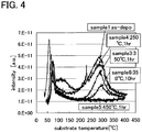
- FIG. 4 is a graph showing comparison of samples, which shows TDS measurement results of H 2 O.
- the comparison was performed on the following samples: the sample (Sample 1) where an In-Ga-Zn-O-based non-single-crystal film with a set thickness of 50 nm is formed over a glass substrate; a sample (Sample 4) where the structure of Sample 1 is subjected to heat treatment for an hour at 250 °C under a nitrogen atmosphere; the sample (Sample 3) where the structure of Sample 1 is subjected to heat treatment for an hour at 350 °C under a nitrogen atmosphere; a sample (Sample 5) where the structure of Sample 1 is subjected to heat treatment for an hour at 450 °C under a nitrogen atmosphere; and a sample (Sample 6) where the structure of Sample 1 is subjected to heat treatment for 10 hours at 350 °C under a nitrogen atmosphere.
- peaks can be confirmed: a first peak in the vicinity of 200 °C to 250 °C, which indicates discharge of impurities such as moisture (H 2 O); and a second peak at 300 °C or higher, which indicates discharge of impurities such as moisture (H 2 O).
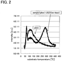
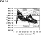
- FIG. 1 shows measurement results of carrier concentrations. Conditions of heat temperature under a nitrogen atmosphere were set to 150 °C, 175 °C, 200 °C, 225 °C, 250 °C, 275 °C, 300 °C, 325 °C, 350 °C, 375 °C, 400 °C, 425 °C, and 450 °C, and a carrier concentration at each temperature was measured.
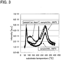
- FIG. 5A illustrates a three-dimensional view of a property-evaluation sample 510 for evaluating properties (the carrier concentrations and Hall mobility) of an oxide semiconductor film (an In-Ga-Zn-O-based non-single-crystal film).
- the property-evaluation sample 510 was fabricated and subjected to Hall effect measurement at room temperature. The carrier concentration and Hall mobility of the oxide semiconductor film were evaluated.
- the property-evaluation sample 510 was fabricated in the following manner: an insulating film 501 including silicon oxynitride was formed over a substrate 500, an oxide semiconductor film 502 with a size of 10 mm ⁇ 10 mm, which serves as an evaluation object, was formed over the insulating film 501, and electrodes 503 to 506 each having a diameter of 1 mm were formed over the oxide semiconductor film 502.
- the carrier concentrations of the oxide semiconductor film obtained by the Hall effect measurement are shown in FIG. 1
- the Hall mobility thereof is shown in FIG. 5B
- conductivity thereof is shown in FIG. 5C .
- H, O, OH, H 2 , O 2 , N, N 2 , and Ar, in addition to H 2 O were each measured by TDS.
- the measurement resulted in that peaks of H 2 O, H, O, and OH were observed clearly but peaks of H 2 , O 2 , N, N 2 , and Ar were not observed.
- samples of the above measurement a structure where an In-Ga-Zn-O-based non-single-crystal film with a set thickness of 50 nm was formed over a glass substrate was used.
- heat treatment for dehydration or dehydrogenation heat treatment performed under an inert-gas atmosphere of nitrogen or an inert gas such as argon or helium or under reduced pressure.
- dehydrogenation does not indicate elimination of only H 2 by heat treatment.
- elimination of H, OH, and the like is referred to as “dehydration or dehydrogenation”.
- Impurities (H 2 O) contained in an oxide semiconductor layer is reduced and the carrier concentration are increased by heat treatment performed under an inert gas, and then slow cooling is performed. After slow cooling, the carrier concentration in the oxide semiconductor layer is reduced by formation of an oxide insulating film in contact with the oxide semiconductor layer or the like, which leads to improvement in reliability.
- the carrier concentration is increased, preferably to 1 ⁇ 10 18 /cm 3 or higher
- the carrier concentration is reduced, preferably to lower than 1 ⁇ 10 18 /cm 3 , more preferably 1 ⁇ 10 14 /cm 3 or lower.
- an inorganic insulating film which blocks impurities such as moisture, hydrogen ions, and OH - is used as the oxide insulating film formed to be in contact with the low-resistance oxide semiconductor layer.
- an inorganic insulating film which blocks impurities such as moisture, hydrogen ions, and OH - is used as the oxide insulating film formed to be in contact with the low-resistance oxide semiconductor layer.
- a silicon oxide film or a silicon nitride oxide film is used as a silicon nitride oxide film.
- second heat treatment may be performed after formation of the oxide insulating film serving as a protective film to be over and in contact with the oxide semiconductor layer.
- variation in electric characteristics of thin film transistors can be reduced.
- One embodiment of the present invention disclosed in this specification is a semiconductor device including a gate electrode layer, a gate insulating layer over the gate electrode layer, an oxide semiconductor layer over the gate insulating layer, and an insulating layer over the oxide semiconductor layer.
- the gate insulating layer, the oxide semiconductor layer, the insulating layer, an interface between the gate insulating layer and the oxide semiconductor layer, and an interface between the oxide semiconductor layer and the insulating layer have a hydrogen concentration of 3 ⁇ 10 20 cm -3 or lower.
- SIMS secondary ion mass spectrometry
- One embodiment of the present invention to realize the above structure is a method for manufacturing a semiconductor device including the steps of forming a gate electrode layer, forming a gate insulating layer over the gate electrode layer, forming an oxide semiconductor layer over the gate insulating layer, performing dehydration or dehydrogenation on the oxide semiconductor layer, forming a source electrode layer and a drain electrode layer over the dehydrated or dehydrogenated oxide semiconductor layer, and forming an oxide insulating film which is in contact with a part of the oxide semiconductor layer and over the gate insulating layer, the oxide semiconductor layer, the source electrode layer, and the drain electrode layer.
- dehydration or dehydrogenation is heat treatment performed under a nitrogen atmosphere or a rare gas atmosphere or under reduced pressure.
- Another embodiment of the present invention to realize the above structure is a method for manufacturing a semiconductor device including the steps of forming a gate electrode layer, forming a gate insulating layer over the gate electrode layer, forming an oxide semiconductor layer over the gate insulating layer, heating the oxide semiconductor layer under an inert atmosphere to increase a carrier concentration, forming a source electrode layer and a drain electrode layer over the oxide semiconductor layer whose carrier concentration is increased, and forming an oxide insulating film which is in contact with a part of the heated oxide semiconductor layer and over the gate insulating layer, the heated oxide semiconductor layer, the source electrode layer, and the drain electrode layer, so that a carrier concentration is reduced.
- the oxide semiconductor layer is heated under an inert atmosphere at a temperature of 400 °C or higher, slow cooling is performed to a temperature which is equal to higher than room temperature and lower than 100 °C.
- Another embodiment of the present invention to realize the above structure is a method for manufacturing a semiconductor device including the steps of forming a gate electrode layer, forming a gate insulating layer over the gate electrode layer, forming an oxide semiconductor layer over the gate insulating layer, heating the oxide semiconductor layer under a reduced pressure to increase a carrier concentration, forming a source electrode layer and a drain electrode layer over the oxide semiconductor layer whose carrier concentration is increased, and forming an oxide insulating film which is in contact with a part of the heated oxide semiconductor layer and over the gate insulating layer, the heated oxide semiconductor layer, and the source electrode layer, and the drain electrode layer, so that a carrier concentration is reduced.
- the oxide semiconductor used in this specification is, for example, a thin film expressed by InMO 3 (ZnO) m (m>0), and a thin film transistor using the thin film as a semiconductor layer is manufactured.
- M denotes one metal element or a plurality of metal elements selected from Ga, Fe, Ni, Mn, and Co.
- M denotes Ga in some cases; meanwhile, M denotes the above metal element such as Ni or Fe in addition to Ga (Ga and Ni or Ga and Fe) in other cases.
- the above oxide semiconductor may include Fe or Ni, another transitional metal element, or an oxide of the transitional metal as an impurity element in addition to the metal element included as M.
- any of the following oxide semiconductors can be applied in addition to the above: an In-Sn-Zn-O-based oxide semiconductor; an In-Al-Zn-O-based oxide semiconductor; a Sn-Ga-Zn-O-based oxide semiconductor; an Al-Ga-Zn-O-based oxide semiconductor; a Sn-Al-Zn-O-based oxide semiconductor; an In-Zn-O-based oxide semiconductor; an In-Ga-O-based oxide semiconductor; a Sn-Zn-O-based oxide semiconductor; an Al-Zn-O-based oxide semiconductor; an In-O-based oxide semiconductor; a Sn-O-based oxide semiconductor; and a Zn-O-based oxide semiconductor.
- the oxide semiconductor preferably includes In, further preferably, includes In and Ga. Dehydration or dehydrogenation is effective in a process of forming an i-type (intrinsic) oxide semiconductor layer.
- a protective circuit for protecting the driver circuit is preferably provided over the same substrate as a gate line or a source line.
- the protective circuit is preferably formed with a non-linear element including an oxide semiconductor.
- a substrate transfer step an alignment step, a slow cooling step, a heating or cooling a substrate step which is for setting the substrate to have temperature suitable to the second film formation step, or the like.
- a thin film transistor having stable electric characteristics can be provided. Further, a semiconductor device which includes thin film transistors having excellent electric characteristics and high reliability can be provided.
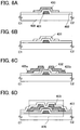
- FIGS. 6A to 6D and FIGS. 7A and 7B A semiconductor device and a method for manufacturing a semiconductor device will be described with reference to FIGS. 6A to 6D and FIGS. 7A and 7B .
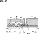
- FIG. 7A is a top view of a thin film transistor 470 of a semiconductor device
- FIG. 7B is a cross-sectional view along line C1-C2 of FIG. 7A
- the thin film transistor 470 is a bottom-gate thin film transistor and includes, over a substrate 400 which is a substrate having an insulating surface, a gate electrode layer 401, a gate insulating layer 402, a semiconductor layer 403, and source and drain electrode layers 405a and 405b.
- an oxide insulating film 407 is provided to cover the thin film transistor 470 and be in contact with the semiconductor layer 403.
- the carrier concentration of the oxide semiconductor layer is reduced by formation of an oxide insulating film to be in contact with the oxide semiconductor layer or the like, which improves reliability of the thin film transistor 470.
- the heat treatment causes reduction in impurities such as moisture inside the gate insulating layer 402 and in interfaces provided between the semiconductor layer 403 formed using an oxide semiconductor and films which are over and below the semiconductor layer 403 to be in contact therewith.
- the interfaces indicate an interface between the gate insulating layer 402 and the semiconductor layer 403 and an interface between the oxide insulating film 407 and the semiconductor layer 403.
- the temperature of a substrate over which a thin film transistor is formed (substrate temperature) is set at fixed temperature, a source and a drain of the thin film transistor are set at the same potential, and a gate is supplied with potential different from those of the source and the drain for a certain period.
- the substrate temperature may be set as appropriate in accordance with the purpose of the test.
- a test in the case where potential applied to the gate is higher than potentials of the source and the drain is referred to as a +BT test
- a test in the case where potential applied to the gate is lower than potentials of the source and the drain is referred to as a -BT test.
- the stress conditions for the BT test can be determined by setting the substrate temperature, electric field intensity applied to a gate insulating film, or a time period of application of electric field.
- the electric field intensity applied to a gate insulating film can be determined by dividing the potential difference between the gate potential and the source and drain potential by the thickness of the gate insulating film. For example, in the case where the electric field intensity applied to the 100-nm-thick gate insulating film is to be set to 2 MV/cm, the potential difference may be set to 20 V.
- a +BT test and a -BT test were performed under such conditions that a substrate temperature was 150 °C, an electric field intensity applied to a gate insulating film was 2 MV/cm, and a time period for application was one hour.
- the +BT test is described.
- a change in characteristics of the source-drain current (hereinafter, referred to as the drain current) was measured, under the conditions where the substrate temperature was set to 40 °C, the voltage between source and drain (hereinafter, the drain voltage) was set to 10 V, and the voltage between source and gate (hereinafter, the gate voltage) was changed in the range of -20 V to +20 V. That is, Vg-Id characteristics were measured.
- the substrate temperature was set to 40 °C.
- the measurement may be performed at room temperature (25 °C) or lower if there is no particular problem.
- the BT test it is important to use a thin film transistor which has been never subjected to a BT test. For example, if a -BT test is performed with use of a thin film transistor which has been once subjected to a +BT test, the results of the -BT test cannot be evaluated correctly due to influence of the +BT test which has been performed previously. Similarly, if the thin film transistor which has been once subjected to a +BT test is used for another +BT test, the results cannot be evaluated correctly.
- the usage of the thin film transistor is not limited to the above in the case where the BT test is performed repeatedly in consideration of such influence.
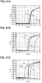
- the horizontal axis represents the gate voltage (Vg) which is shown with a logarithmic scale
- the vertical axis represents the drain current (Id) which is shown with a logarithmic scale.
- Initial characteristics 711, 721, and 731 indicate the Vg-Id characteristics of the thin film transistors before the +BT tests
- +BTs 712, 722, and 732 indicate the Vg-Id characteristics of the thin film transistors after +BT tests
- -BTs 713, 723, and 733 indicate the Vg-Id characteristics of the thin film transistors after -BT tests. Note that the Vg-Id characteristics of the thin film transistors before the -BT tests are almost the same as those before the +BT tests; thus, they are not shown in the graphs.
- Heat treatment is performed on the oxide semiconductor layer under an atmosphere of an inert gas (such as nitrogen, helium, neon, or argon) or under reduced pressure, and then, slow cooling is performed under an inert atmosphere (see FIG. 6B ).
- an inert gas such as nitrogen, helium, neon, or argon
- slow cooling is performed under an inert atmosphere (see FIG. 6B ).
- nitrogen or a rare gas such as helium, neon, or argon it is preferable that moisture, hydrogen, and the like be not contained in nitrogen or a rare gas such as helium, neon, or argon.
- nitrogen or a rare gas such as helium, neon, or argon introduced into an apparatus for heat treatment have purity of 6N (99.9999 %) or more, preferably, 7N (99.99999 %) or more; that is, an impurity concentration is set to 1 ppm or lower, preferably, 0.1 ppm or lower.
- FIG. 14 is a schematic view of the electric furnace 601.
- Heaters 603 are provided outside a chamber 602, which heats the chamber 602. Inside the chamber 602, a susceptor 605 in which a substrate 604 is mounted is provided. The substrate 604 is transferred into/from the chamber 602.
- the chamber 602 is provided with a gas supply means 606 and an evacuation means 607. With the gas supply means 606, a gas is introduced into the chamber 602.
- the evacuation means 607 exhausts the inside of the chamber 602 or reduces the pressure in the chamber 602.
- the temperature rising characteristics of the electric furnace is preferably set to from 0.1 °C/min to 20 °C/min.
- the temperature decreasing characteristics of the electric furnace is preferably set to from 0.1 °C/min to 15 °C/min.
- nitrogen or a rare gas is introduced into the chamber 602 from the gas supply source 611, so that the inside of the chamber 602 is in a nitrogen or a rare gas atmosphere.
- the oxide semiconductor layer 430 formed over the substrate 604 is heated, whereby the oxide semiconductor layer 430 can be dehydrated or dehydrogenated.
- an element selected from Al, Cr, Ta, Ti, Mo, and W; an alloy containing any of the above elements as its component; an alloy film containing a combination of any of the above elements; and the like can be given.
- the oxide insulating film 407 is formed by a sputtering method, a PCVD method, or the like to be in contact with the low-resistance oxide semiconductor layer 432, in the low-resistance oxide semiconductor layer 432, at least a region in contact with the oxide insulating film 407 have increased resistance (i.e., the carrier concentration is reduced, preferably to lower than 1 ⁇ 10 18 /cm 3 ). Thus, a high-resistance oxide semiconductor region can be obtained.
- the oxide semiconductor layer 432 becomes the semiconductor layer 403 having a high-resistance oxide semiconductor region (a third oxide semiconductor layer), and then, the thin film transistor 470 can be completed (see FIG. 6D ).
- heat treatment may be performed on the thin film transistor 470, under a nitrogen atmosphere or an air atmosphere (in air) at temperature equal to or higher than 150 °C and lower than 350 °C, preferably.
- heat treatment under a nitrogen atmosphere at 250 °C is performed for one hour.
- the oxide semiconductor layer 432 in a condition of being in contact with the oxide insulating film 407 is heated; thus, variation in electric characteristics of the thin film transistor 470 can be reduced.
- this heat treatment at temperature equal to or higher than 150 °C and lower than 350 °C, preferably
- this heat treatment also serves as heat treatment in another step, e.g., heat treatment in formation of a resin film or heat treatment for reducing resistance of a transparent conductive film, the number of steps can be prevented from increasing.
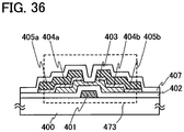
- the source and drain electrode layers 455a and 455b in contact with the semiconductor layer 453 which is an oxide semiconductor layer is formed using one or more materials selected from titanium, aluminum, manganese, magnesium, zirconium, and beryllium.
- a conductive film is formed and patterned into island-shaped source and drain electrode layers 455a and 455b by a photolithography step ( FIG. 8A ).
- the material of the source and drain electrode layers 455a and 455b there are an element selected from Al, Cr, Ta, Ti, Mo, and W, an alloy including any of these elements as its component, an alloy including a combination of any of these elements, and the like. Further, an alloy film including these elements in combination, and the like, may be stacked.
- Heat treatment for dehydration or dehydrogenation is performed on the oxide semiconductor layer 483, and then, slow cooling is performed under an inert atmosphere.
- heat treatment for dehydration or dehydrogenation heat treatment is performed under an inert gas (such as nitrogen, helium, neon, or argon) atmosphere or under reduced pressure at temperature of from 200 °C to 600 °C inclusive, preferably, from 400 °C to 450 °C inclusive.
- resistance of the oxide semiconductor layer 483 is reduced (i.e., the carrier concentration is increased, preferably to 1 ⁇ 10 18 /cm 3 or higher), so that a low-resistance oxide semiconductor layer 484 (a second oxide semiconductor layer) can be obtained (see FIG. 8C ).
- moisture, hydrogen, and the like be not contained in nitrogen or a rare gas such as helium, neon, or argon.
- nitrogen or a rare gas such as helium, neon, or argon introduced into an apparatus for heat treatment have purity of 6N (99.9999 %) or more, preferably, 7N (99.99999 %) or more; that is, an impurity concentration is set to 1 ppm or lower, preferably, 0.1 ppm or lower.
- the oxide insulating film 457 is formed by a sputtering method to be in contact with the low-resistance oxide semiconductor layer 484, in the low-resistance oxide semiconductor layer 484, at least a region in contact with the oxide insulating film 457 which is a silicon oxide film have increased resistance (i.e., the carrier concentration is reduced, preferably to lower than 1 ⁇ 10 18 /cm 3 ). Thus, a high-resistance oxide semiconductor region can be obtained.
- it is important to increase and decrease the carrier concentration in the oxide semiconductor layer by performance of heat treatment and slow cooling under an inert-gas atmosphere (or under reduced pressure), formation of an oxide insulating film, and the like.
- the oxide semiconductor layer 484 becomes the semiconductor layer 453 having the high-resistance oxide semiconductor region (a third oxide semiconductor layer), and then, the thin film transistor 460 can be completed (see FIG. 8D ).
- Impurities (such as H 2 O, H, and OH) contained in the oxide semiconductor layer are reduced by performance of heat treatment for dehydration or dehydrogenation, and the carrier concentration is increased. After that, slow cooling is performed. Then, formation of an oxide insulating film in contact with the oxide semiconductor layer, or the like, is performed, so that the carrier concentration of the oxide semiconductor layer is reduced. Thus, reliability of the thin film transistor 460 can be improved.
- heat treatment may be performed on the thin film transistor 460, under a nitrogen atmosphere or an air atmosphere (in air) at temperature equal to or higher than 150 °C and lower than 350 °C, preferably.
- heat treatment is performed under a nitrogen atmosphere at 250 °C for one hour.
- the semiconductor layer 453 in a condition being in contact with the oxide insulating film 457 is heated; thus, variation in electric characteristics of the thin film transistor 460 can be reduced.
- this heat treatment at equal to or higher than 150 °C and lower than 350 °C, preferably
- this heat treatment also serves as heat treatment in another step, e.g., heat treatment in formation of a resin film or heat treatment for reducing resistance of a transparent conductive film, the number of steps can be prevented from increasing.
- Embodiment 1 can be freely combined with Embodiment 1.
- FIGS. 10A to 10D A manufacturing process of a semiconductor device including a thin film transistor will be described with reference to FIGS. 10A to 10D , FIGS. 11A to 11C , FIG. 12 , and FIGS. 13A1, 13A2, 13B1, and 13B2 .
- a conductive layer is formed over an entire surface of the substrate 100, and then a first photolithography step is performed.
- a resist mask is formed, and then an unnecessary portion is removed by etching, so that wirings and electrodes (a gate wiring including a gate electrode layer 101, a capacitor wiring 108, and a first terminal 121) are formed.
- the etching is performed so that at least end portions of the gate electrode layer 101 have a tapered shape.
- a gate insulating layer 102 is formed over the entire surface of the gate electrode layer 101.
- the gate insulating layer 102 is formed to a thickness of 50 to 250 nm by a PCVD method, a sputtering method, or the like.
- an oxide semiconductor film (an In-Ga-Zn-O-based non-single-crystal film) is formed over the gate insulating layer 102. It is effective to form the In-Ga-Zn-O-based non-single-crystal film without exposure to air after the plasma treatment because dust and moisture do not adhere to the interface between the gate insulating layer and the semiconductor film.
- Examples of a sputtering method include an RF sputtering method in which a high-frequency power source is used as a sputtering power source, a DC sputtering method, and a pulsed DC sputtering method in which a bias is applied in a pulsed manner.
- An RF sputtering method is mainly used in the case where an insulating film is formed, and a DC sputtering method is mainly used in the case where a metal film is formed.
- a deposition method using sputtering there are also a reactive sputtering method in which a target substance and a sputtering gas component are chemically reacted with each other during deposition to form a thin compound film thereof, and a bias sputtering in which a voltage is also applied to a substrate during deposition.
- etching gas for dry etching a gas containing chlorine (chlorine-based gas such as chlorine (Cl 2 ), boron chloride (BCl 3 ), silicon chloride (SiCl 4 ), or carbon tetrachloride (CCl 4 )) is preferably used.
- the conductive film When heat treatment is performed after the conductive film 132 is formed, the conductive film preferably has heat resistance enough to withstand this heat resistance.
- Heat treatment may be performed under an oxygen atmosphere before formation of the protective insulating layer 107.
- the heat treatment under an oxygen atmosphere may be performed at a temperature higher than or equal to 150 °C and lower than 350 °C.
- a fifth photolithography step is performed.
- a resist mask is formed, and an unnecessary portion of the transparent conductive film is removed by etching to form a pixel electrode layer 110.
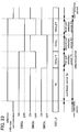
- a driving method called double-frame rate driving may be employed in which a vertical synchronizing frequency is 1.5 times or more, preferably, 2 times or more as high as a usual vertical synchronizing frequency to improve the moving-image characteristics.
- the display characteristics of a liquid crystal display device such as moving-image characteristics, can be improved as compared to those of conventional liquid crystal display devices.
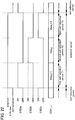
- the signal line driver circuit of FIG. 21 to which the timing chart of FIG. 23 is applied, the signal line can be pre-charged by providing the pre-charge period before the sub-selection periods.
- a video signal can be written to a pixel with high speed.
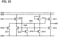
- a first electrode of the seventh thin film transistor 5577 is connected to the sixth wiring 5506.
- a second electrode of the seventh thin film transistor 5577 is connected to the gate electrode of the first thin film transistor 5571.
- a gate electrode of the seventh thin film transistor 5577 is connected to the second wiring 5502.
- a first electrode of the eighth thin film transistor 5578 is connected to the sixth wiring 5506.
- a second electrode of the eighth thin film transistor 5578 is connected to the gate electrode of the second thin film transistor 5572.
- a gate electrode of the eighth thin film transistor 5578 is connected to the first wiring 5501.
- the points at which the gate electrode of the first thin film transistor 5571, the gate electrode of the fourth thin film transistor 5574, the second electrode of the fifth thin film transistor 5575, the second electrode of the sixth thin film transistor 5576, and the second electrode of the seventh thin film transistor 5577 are connected are each referred to as a node 5543.
- the points at which the gate electrode of the second thin film transistor 5572, the second electrode of the third thin film transistor 5573, the second electrode of the fourth thin film transistor 5574, the gate electrode of the sixth thin film transistor 5576, and the second electrode of the eighth thin film transistor 5578 are connected are each referred to as a node 5544.
- first substrate 4001 and the second substrate 4006 can be formed of glass, metal (typically, stainless steel), ceramic, or plastic.
- plastic a fiberglass-reinforced plastics (FRP) plate, a polyvinyl fluoride (PVF) film, a polyester film, or an acrylic resin film can be used.
- FRP fiberglass-reinforced plastics
- PVF polyvinyl fluoride
- polyester film a polyester film
- acrylic resin film acrylic resin film
- a sheet with a structure in which an aluminum foil is sandwiched between PVF films or polyester films can be used.
- the insulating layer 4020 having a stacked-layer structure is formed as a protective film.
- a silicon oxide film is formed by a sputtering method.
- the use of a silicon oxide film as a protective film has an effect of preventing hillock of an aluminum film used for the source and drain electrode layers.
- the pixel electrode layer 4030 and the counter electrode layer 4031 can be formed using a light-transmitting conductive material such as indium oxide containing tungsten oxide, indium zinc oxide containing tungsten oxide, indium oxide containing titanium oxide, indium tin oxide containing titanium oxide, indium tin oxide (hereinafter referred to as ITO), indium zinc oxide, indium tin oxide to which silicon oxide is added, or the like.
- a light-transmitting conductive material such as indium oxide containing tungsten oxide, indium zinc oxide containing tungsten oxide, indium oxide containing titanium oxide, indium tin oxide containing titanium oxide, indium tin oxide (hereinafter referred to as ITO), indium zinc oxide, indium tin oxide to which silicon oxide is added, or the like.
- a light source includes a cold cathode tube 2610 and a reflective plate 2611, and a circuit board 2612 is connected to a wiring circuit portion 2608 of the TFT substrate 2600 by a flexible wiring board 2609 and includes an external circuit such as a control circuit or a power source circuit.
- the polarizing plate and the liquid crystal layer may be stacked with a retardation plate therebetween.
- the liquid crystal display module can employ a TN (Twisted Nematic) mode, an IPS (In-Plane-Switching) mode, an FFS (Fringe Field Switching) mode, an MVA (Multi-domain Vertical Alignment) mode, a PVA (Patterned Vertical Alignment) mode, an ASM (Axially Symmetric aligned Micro-cell) mode, an OCB (Optical Compensated Birefringence) mode, an FLC (Ferroelectric Liquid Crystal) mode, an AFLC (Anti Ferroelectric Liquid Crystal) mode, or the like.
- TN Transmission Nematic
- IPS In-Plane-Switching
- FFS Fe Field Switching
- MVA Multi-domain Vertical Alignment
- PVA Powerned Vertical Alignment
- ASM Accelerd Vertical Alignment
- OCB Optical Compensated Birefringence
- FLC Fluorroelectric Liquid Crystal
- AFLC Anti Ferro
- the electrophoretic display element has higher reflectance than a liquid crystal display element, and thus, an auxiliary light is unnecessary, power consumption is low, and a display portion can be recognized in a dim place. In addition, even when power is not supplied to the display portion, an image which has been displayed once can be maintained. Accordingly, a displayed image can be stored even if a semiconductor device having a display function (which may be referred to simply as a display device or a semiconductor device provided with a display device) is distanced from an electric wave source.
- a semiconductor device having a display function which may be referred to simply as a display device or a semiconductor device provided with a display device
- FIG. 18 illustrates an example of a pixel structure to which digital time grayscale driving can be applied, as an example of a semiconductor device.
- the pixel structure illustrated in FIG. 18 is not limited thereto.
- a switch, a resistor, a capacitor, a transistor, a logic circuit, or the like may be added to the pixel illustrated in FIG. 18 .
- a light-blocking film 7016 for reflecting or blocking light may be formed to cover the anode 7015 when the anode 7015 has a light-transmitting property.
- the cathode 7013 a variety of materials can be used as in the case of FIG. 19A as long as they are conductive materials having a low work function.
- the cathode 7013 is formed to have a thickness that can transmit light (preferably, approximately 5 nm to 30 nm).
- an aluminum film with a thickness of 20 nm can be used as the cathode 7013.
- the light-emitting layer 7014 may be formed using either a single layer or a plurality of layers stacked.
- a 20-nm-thich aluminum film can be used as the cathode 7023.
- the light-emitting layer 7024 may be formed using either a single layer or a plurality of layers stacked.
- the anode 7025 can be formed using a light-transmitting conductive material as in the case of FIG. 19A .
- the structure of the semiconductor device is not limited to those illustrated in FIGS. 19A to 19C and can be modified in various ways based on techniques disclosed in this specification.
- the pixel portion 4502, the signal line driver circuits 4503a and 4503b, and the scan line driver circuits 4504a and 4504b formed over the first substrate 4501 each include a plurality of thin film transistors, and a thin film transistor 4510 included in the pixel portion 4502 and a thin film transistor 4509 included in the signal line driver circuit 4503a are illustrated as an example in FIG. 17B .
- a connection terminal electrode 4515 is formed from the same conductive film as the first electrode layer 4517 included in the light-emitting element 4511, and a terminal electrode 4516 is formed from the same conductive film as the source and drain electrode layers included in the thin film transistors 4509 and 4510.
- connection terminal electrode 4515 is electrically connected to a terminal included in the FPC 4518a via an anisotropic conductive film 4519.
- FIG. 27 illustrates an example of an e-book reader 2700.
- the e-book reader 2700 includes two housings, a housing 2701 and a housing 2703.
- the housing 2701 and the housing 2703 are combined with a hinge 2711 so that the e-book reader 2700 can be opened and closed with the hinge 2711 as an axis.
- the e-book reader 2700 can operate like a paper book.
- FIG. 29B illustrates an example of a slot machine 9900 which is a large-sized game machine.
- a display portion 9903 is incorporated in a housing 9901.
- the slot machine 9900 includes an operation means such as a start lever or a stop switch, a coin slot, a speaker, and the like. It is needless to say that the structure of the slot machine 9900 is not limited to the above and other structures provided with at least a semiconductor device disclosed in this specification may be employed.
- the slot machine 9900 may include other accessory equipment as appropriate.
- the main body includes a camera portion 9206 including an image pick-up means having a function of converting an image of an object, which is formed through a camera lens, to an electronic image signal.
- the camera portion is not necessarily provided.
- the mobile phone illustrated in FIG. 30B is provided with a receiver of a television broadcast and the like, and can display an image on the display portion 9201 by receiving a television broadcast.
- the mobile phone illustrated in FIG. 30B is provided with a memory device and the like such as a memory, and can record a television broadcast in the memory.
- the mobile phone illustrated in FIG. 30B may have a function of collecting location information, such as the GPS.
- FIG. 32 is a cross-sectional view of the thin film transistor 471 included in a semiconductor device.
- the thin film transistor 471 is a bottom-gate thin film transistor and includes, over the substrate 400 which is a substrate having an insulating surface, the gate electrode layer 401, the gate insulating layer 402, the semiconductor layer 403, the source and drain electrode layers 405a and 405b, and the conductive layer 409.
- the conductive layer 409 is provided over the oxide insulating film 407 so as to overlap with the gate electrode layer 401.
- a semiconductor device and a method for manufacturing a semiconductor device will be described with reference to FIG 33 .
- the same portion as or a portion having similar function to those described in Embodiment 1 can be formed in a manner similar to that described in Embodiment 1; therefore, repetitive description is omitted.
- FIG. 33 is a cross-sectional view of the thin film transistor 472 included in a semiconductor device.
- the thin film transistor 472 is a bottom-gate thin film transistor and includes, over the substrate 400 which is a substrate having an insulating surface, the gate electrode layer 401, the gate insulating layer 402, the semiconductor layer 403, source and drain regions 404a and 404b, the source and drain electrode layers 405a and 405b, and the conductive layer 419.
- the conductive layer 419 is provided over the oxide insulating film 407 and the insulating layer 410 to overlap with the gate electrode layer 401.
- the insulating layer 410 serving as a planarization film is stacked over the oxide insulating film 407, and an opening which reaches the source or drain electrode layer 405b is formed in the oxide insulating film 407 and the insulating layer 410.
- a conductive film is formed over the insulating layer 410 and in the opening formed in the oxide insulating film 407 and the insulating layer 410, and etched into a desired shape, so that the conductive layer 419 and a pixel electrode layer 411 are formed.
- the conductive layer 419 can be formed together with the pixel electrode layer 411, using the same material by the same method.
- the pixel electrode layer 411 and the conductive layer 419 are formed using indium oxide-tin oxide alloy containing silicon oxide (an In-Sn-O based oxide containing silicon oxide).
- dehydration or dehydrogenation is performed.
- the channel protective layer 1418 can be formed using an inorganic material including oxygen (such as silicon oxide, silicon oxynitride, or silicon nitride oxide).
- oxygen such as silicon oxide, silicon oxynitride, or silicon nitride oxide.
- a vapor deposition method such as a plasma CVD method or a thermal CVD method or a sputtering method can be used.
- the channel protective layer 1418 is processed by etching a shape of a deposited film.
- the channel protective layer 1418 is formed in such a manner that a silicon oxide film is formed by a sputtering method and processed by etching using a mask formed by photolithography.
- this embodiment is not limited to the above-described structure including the n + layers 1406a and 1406b; a structure in which an n + layer is not provided may be employed.
- the conductive layer 1409 can be formed using a material similar to that of the gate electrode layer 1401 or the source and drain electrode layers 1405a and 1405b by a method similar thereto. In the case where a pixel electrode layer is provided, the conductive layer 1409 may be formed using a material similar to that of the pixel electrode layer by a method similar thereto. In this embodiment, a stack of a titanium film, an aluminum film, and a titanium film is used as the conductive layer 1409.
- FIG. 35B illustrates an example partly different from FIG. 35A .
- the same portion and a step as, or a portion having function similar to those illustrated in FIG 35A can be made in a manner similar to that illustrated in FIG. 35A ; therefore, repetitive description is omitted.
- heat treatment is performed under an atmosphere of an inert gas (such as nitrogen, helium, neon, or argon) or under reduced pressure, and then slow cooling is performed.
- an inert gas such as nitrogen, helium, neon, or argon
- Heat treatment performed on the first oxide semiconductor layer under the above atmosphere makes it possible to eliminate impurities such as hydrogen and moisture in an oxide semiconductor layer 403.
- FIG. 42 illustrates a model of an oxide semiconductor layer which was used for the simulation.
- a structure in which a layer 1203 having low oxygen density and a layer 1205 having high oxygen density were stacked was employed for an oxide semiconductor layer 1201.
Applications Claiming Priority (3)
| Application Number | Priority Date | Filing Date | Title |
|---|---|---|---|
| JP2009156410 | 2009-06-30 | ||
| EP10794048.8A EP2449594B1 (fr) | 2009-06-30 | 2010-06-16 | Procédé de fabrication de dispositif à semi-conducteurs |
| PCT/JP2010/060694 WO2011001879A1 (fr) | 2009-06-30 | 2010-06-16 | Procédé de fabrication de dispositif à semi-conducteurs |
Related Parent Applications (2)
| Application Number | Title | Priority Date | Filing Date |
|---|---|---|---|
| EP10794048.8A Division EP2449594B1 (fr) | 2009-06-30 | 2010-06-16 | Procédé de fabrication de dispositif à semi-conducteurs |
| EP10794048.8A Division-Into EP2449594B1 (fr) | 2009-06-30 | 2010-06-16 | Procédé de fabrication de dispositif à semi-conducteurs |
Publications (1)
| Publication Number | Publication Date |
|---|---|
| EP3573108A1 true EP3573108A1 (fr) | 2019-11-27 |
Family
ID=43410954
Family Applications (2)
| Application Number | Title | Priority Date | Filing Date |
|---|---|---|---|
| EP19185984.2A Withdrawn EP3573108A1 (fr) | 2009-06-30 | 2010-06-16 | Procédé de fabrication d'un dispositif semi-conducteur |
| EP10794048.8A Active EP2449594B1 (fr) | 2009-06-30 | 2010-06-16 | Procédé de fabrication de dispositif à semi-conducteurs |
Family Applications After (1)
| Application Number | Title | Priority Date | Filing Date |
|---|---|---|---|
| EP10794048.8A Active EP2449594B1 (fr) | 2009-06-30 | 2010-06-16 | Procédé de fabrication de dispositif à semi-conducteurs |
Country Status (7)
| Country | Link |
|---|---|
| US (6) | US8557641B2 (fr) |
| EP (2) | EP3573108A1 (fr) |
| JP (11) | JP5459909B2 (fr) |
| KR (8) | KR20200031709A (fr) |
| CN (3) | CN106409684B (fr) |
| TW (6) | TWI623046B (fr) |
| WO (1) | WO2011001879A1 (fr) |
Cited By (1)
| Publication number | Priority date | Publication date | Assignee | Title |
|---|---|---|---|---|
| US10741414B2 (en) | 2013-10-10 | 2020-08-11 | Semiconductor Energy Laboratory Co., Ltd. | Semiconductor device |
Families Citing this family (45)
| Publication number | Priority date | Publication date | Assignee | Title |
|---|---|---|---|---|
| WO2011001881A1 (fr) | 2009-06-30 | 2011-01-06 | Semiconductor Energy Laboratory Co., Ltd. | Procédé de fabrication de dispositif à semi-conducteurs |
| CN106409684B (zh) | 2009-06-30 | 2020-01-21 | 株式会社半导体能源研究所 | 用于制造半导体器件的方法 |
| KR101604577B1 (ko) | 2009-06-30 | 2016-03-17 | 가부시키가이샤 한도오따이 에네루기 켄큐쇼 | 반도체 장치 제조 방법 |
| KR101810699B1 (ko) | 2009-06-30 | 2018-01-25 | 가부시키가이샤 한도오따이 에네루기 켄큐쇼 | 반도체 장치 제작 방법 |
| KR102503687B1 (ko) * | 2009-07-03 | 2023-02-27 | 가부시키가이샤 한도오따이 에네루기 켄큐쇼 | 반도체 장치의 제작 방법 |
| SG10201403913PA (en) | 2009-07-10 | 2014-10-30 | Semiconductor Energy Lab | Method for manufacturing semiconductor device |
| TWI559501B (zh) | 2009-08-07 | 2016-11-21 | 半導體能源研究所股份有限公司 | 半導體裝置和其製造方法 |
| WO2011027656A1 (fr) | 2009-09-04 | 2011-03-10 | Semiconductor Energy Laboratory Co., Ltd. | Transistor et dispositif d'affichage |
| KR101791812B1 (ko) | 2009-09-04 | 2017-10-30 | 가부시키가이샤 한도오따이 에네루기 켄큐쇼 | 반도체 장치의 제작 방법 |
| CN107195328B (zh) | 2009-10-09 | 2020-11-10 | 株式会社半导体能源研究所 | 移位寄存器和显示装置以及其驱动方法 |
| KR101370301B1 (ko) | 2009-11-20 | 2014-03-05 | 가부시키가이샤 한도오따이 에네루기 켄큐쇼 | 반도체 장치의 제작 방법 |
| DE112011101069B4 (de) | 2010-03-26 | 2018-05-03 | Semiconductor Energy Laboratory Co., Ltd. | Halbleitervorrichtung und Verfahren zur Herstellung der Halbleitervorrichtung |
| WO2011118741A1 (fr) | 2010-03-26 | 2011-09-29 | Semiconductor Energy Laboratory Co., Ltd. | Procédé de fabrication d'un dispositif semi-conducteur |
| US8906756B2 (en) | 2010-05-21 | 2014-12-09 | Semiconductor Energy Laboratory Co., Ltd. | Method for manufacturing semiconductor device |
| WO2011145484A1 (fr) | 2010-05-21 | 2011-11-24 | Semiconductor Energy Laboratory Co., Ltd. | Dispositif à semi-conducteurs |
| CN105957802A (zh) | 2010-05-21 | 2016-09-21 | 株式会社半导体能源研究所 | 半导体装置及其制造方法 |
| US8441010B2 (en) | 2010-07-01 | 2013-05-14 | Semiconductor Energy Laboratory Co., Ltd. | Semiconductor device |
| WO2012014952A1 (fr) | 2010-07-27 | 2012-02-02 | Semiconductor Energy Laboratory Co., Ltd. | Dispositif à semi-conducteur et son procédé de fabrication |
| JP5189674B2 (ja) * | 2010-12-28 | 2013-04-24 | 出光興産株式会社 | 酸化物半導体薄膜層を有する積層構造、積層構造の製造方法、薄膜トランジスタ及び表示装置 |
| US8957442B2 (en) * | 2011-02-11 | 2015-02-17 | Semiconductor Energy Laboratory Co., Ltd. | Light-emitting device and display device |
| JP5766467B2 (ja) | 2011-03-02 | 2015-08-19 | 株式会社東芝 | 薄膜トランジスタ及びその製造方法、表示装置 |
| JP5657434B2 (ja) * | 2011-03-14 | 2015-01-21 | 富士フイルム株式会社 | 酸化物半導体薄膜の製造方法、電界効果型トランジスタ、表示装置及びセンサ |
| US9219159B2 (en) | 2011-03-25 | 2015-12-22 | Semiconductor Energy Laboratory Co., Ltd. | Method for forming oxide semiconductor film and method for manufacturing semiconductor device |
| TWI545652B (zh) | 2011-03-25 | 2016-08-11 | 半導體能源研究所股份有限公司 | 半導體裝置及其製造方法 |
| US9012904B2 (en) * | 2011-03-25 | 2015-04-21 | Semiconductor Energy Laboratory Co., Ltd. | Semiconductor device and method for manufacturing the same |
| JP2012256406A (ja) * | 2011-04-08 | 2012-12-27 | Semiconductor Energy Lab Co Ltd | 記憶装置、及び当該記憶装置を用いた半導体装置 |
| JP2013087962A (ja) * | 2011-10-13 | 2013-05-13 | Panasonic Corp | 加熱調理装置 |
| TWI581431B (zh) * | 2012-01-26 | 2017-05-01 | 半導體能源研究所股份有限公司 | 半導體裝置及半導體裝置的製造方法 |
| US9048265B2 (en) | 2012-05-31 | 2015-06-02 | Semiconductor Energy Laboratory Co., Ltd. | Method for manufacturing semiconductor device comprising oxide semiconductor layer |
| KR102072099B1 (ko) | 2012-11-08 | 2020-01-31 | 가부시키가이샤 한도오따이 에네루기 켄큐쇼 | 금속 산화물 막 및 금속 산화물 막의 형성 방법 |
| KR20230023050A (ko) * | 2012-12-28 | 2023-02-16 | 가부시키가이샤 한도오따이 에네루기 켄큐쇼 | 반도체 장치 |
| JP6401483B2 (ja) | 2013-04-26 | 2018-10-10 | 株式会社半導体エネルギー研究所 | 半導体装置の作製方法 |
| KR102169628B1 (ko) * | 2013-11-26 | 2020-10-23 | 한국전자통신연구원 | 산화물 반도체 형성방법 |
| CA2932446A1 (fr) * | 2013-12-04 | 2015-06-11 | The Governors Of The University Of Alberta | Transistor a couches minces a barriere source de schottky enfouie, et procede de fabrication |
| CN104810263B (zh) * | 2014-01-24 | 2018-11-20 | 北大方正集团有限公司 | 栅氧化层的制造方法 |
| CN106415801B (zh) | 2014-06-03 | 2019-12-13 | 夏普株式会社 | 半导体装置及其制造方法 |
| US20160163869A1 (en) * | 2014-12-08 | 2016-06-09 | Semiconductor Energy Laboratory Co., Ltd. | Transistor |
| CN104576656A (zh) * | 2014-12-23 | 2015-04-29 | 京东方科技集团股份有限公司 | 一种显示基板及其制作方法、显示装置 |
| JP6097808B2 (ja) * | 2015-10-15 | 2017-03-15 | 株式会社ジャパンディスプレイ | 半導体装置及び半導体装置の製造方法 |
| CN107039298B (zh) * | 2016-11-04 | 2019-12-24 | 厦门市三安光电科技有限公司 | 微元件的转移装置、转移方法、制造方法、装置和电子设备 |
| KR102343573B1 (ko) * | 2017-05-26 | 2021-12-28 | 삼성디스플레이 주식회사 | 플렉서블 디스플레이 장치 |
| CN107369716B (zh) * | 2017-07-17 | 2021-02-12 | 京东方科技集团股份有限公司 | 薄膜晶体管及制作方法、显示装置 |
| KR102616996B1 (ko) | 2017-09-05 | 2023-12-27 | 가부시키가이샤 한도오따이 에네루기 켄큐쇼 | 반도체 장치 및 반도체 장치의 제작 방법 |
| KR20210009000A (ko) | 2019-07-16 | 2021-01-26 | 삼성전자주식회사 | 반도체 장치 |
| CN111952317B (zh) * | 2020-08-04 | 2024-04-09 | 长江存储科技有限责任公司 | 三维存储器及其制备方法 |
Citations (14)
| Publication number | Priority date | Publication date | Assignee | Title |
|---|---|---|---|---|
| JPS60198861A (ja) | 1984-03-23 | 1985-10-08 | Fujitsu Ltd | 薄膜トランジスタ |
| JPH08264794A (ja) | 1995-03-27 | 1996-10-11 | Res Dev Corp Of Japan | 亜酸化銅等の金属酸化物半導体による薄膜トランジスタとpn接合を形成した金属酸化物半導体装置およびそれらの製造方法 |
| JPH11505377A (ja) | 1995-08-03 | 1999-05-18 | フィリップス エレクトロニクス ネムローゼ フェンノートシャップ | 半導体装置 |
| JP2000150900A (ja) | 1998-11-17 | 2000-05-30 | Japan Science & Technology Corp | トランジスタ及び半導体装置 |
| JP2004103957A (ja) | 2002-09-11 | 2004-04-02 | Japan Science & Technology Corp | ホモロガス薄膜を活性層として用いる透明薄膜電界効果型トランジスタ |
| US20080038882A1 (en) * | 2006-08-09 | 2008-02-14 | Kazushige Takechi | Thin-film device and method of fabricating the same |
| JP2008141119A (ja) * | 2006-12-05 | 2008-06-19 | Canon Inc | 酸化物半導体を用いた表示装置及びその製造方法 |
| US20080303020A1 (en) * | 2007-05-29 | 2008-12-11 | Hyun-Soo Shin | Thin film transistor, flat panel display device having the same, and associated methods |
| US20090045397A1 (en) * | 2005-09-06 | 2009-02-19 | Canon Kabushiki Kaisha | Field effect transistor using amorphous oxide film as channel layer, manufacturing method of field effect transistor using amorphous oxide film as channel layer, and manufacturing method of amorphous oxide film |
| US20090057674A1 (en) * | 2007-08-28 | 2009-03-05 | Jong-Han Jeong | Thin film transistor, light-emitting display device having the same and associated methods |
| US20090065771A1 (en) * | 2006-03-17 | 2009-03-12 | Canon Kabushiki Kaisha | Field effect transistor using oxide film for channel and method of manufacturing the same |
| WO2009072532A1 (fr) * | 2007-12-04 | 2009-06-11 | Canon Kabushiki Kaisha | Dispositif à semi-conducteur d'oxyde comprenant une couche isolante et appareil d'affichage associé |
| JP2009135380A (ja) * | 2007-05-30 | 2009-06-18 | Canon Inc | 酸化物半導体を用いた薄膜トランジスタの製造方法および表示装置 |
| JP2009156410A (ja) | 2007-12-27 | 2009-07-16 | Toyota Motor Corp | 流量調整器、および、高圧ガス容器 |
Family Cites Families (170)
| Publication number | Priority date | Publication date | Assignee | Title |
|---|---|---|---|---|
| GB2087147B (en) | 1980-11-06 | 1985-03-13 | Nat Res Dev | Methods of manufacturing semiconductor devices |
| JPH0244256B2 (ja) | 1987-01-28 | 1990-10-03 | Kagaku Gijutsucho Mukizaishitsu Kenkyushocho | Ingazn2o5deshimesarerurotsuhoshokeinosojokozoojusurukagobutsuoyobisonoseizoho |
| JPH0244260B2 (ja) | 1987-02-24 | 1990-10-03 | Kagaku Gijutsucho Mukizaishitsu Kenkyushocho | Ingazn5o8deshimesarerurotsuhoshokeinosojokozoojusurukagobutsuoyobisonoseizoho |
| JPS63210023A (ja) | 1987-02-24 | 1988-08-31 | Natl Inst For Res In Inorg Mater | InGaZn↓4O↓7で示される六方晶系の層状構造を有する化合物およびその製造法 |
| JPH0244258B2 (ja) | 1987-02-24 | 1990-10-03 | Kagaku Gijutsucho Mukizaishitsu Kenkyushocho | Ingazn3o6deshimesarerurotsuhoshokeinosojokozoojusurukagobutsuoyobisonoseizoho |
| JPH0244262B2 (ja) | 1987-02-27 | 1990-10-03 | Kagaku Gijutsucho Mukizaishitsu Kenkyushocho | Ingazn6o9deshimesarerurotsuhoshokeinosojokozoojusurukagobutsuoyobisonoseizoho |
| JPH0244263B2 (ja) | 1987-04-22 | 1990-10-03 | Kagaku Gijutsucho Mukizaishitsu Kenkyushocho | Ingazn7o10deshimesarerurotsuhoshokeinosojokozoojusurukagobutsuoyobisonoseizoho |
| JP2652267B2 (ja) * | 1990-10-29 | 1997-09-10 | 株式会社半導体エネルギー研究所 | 絶縁ゲイト型半導体装置 |
| JPH05251705A (ja) | 1992-03-04 | 1993-09-28 | Fuji Xerox Co Ltd | 薄膜トランジスタ |
| JP3625598B2 (ja) | 1995-12-30 | 2005-03-02 | 三星電子株式会社 | 液晶表示装置の製造方法 |
| JP3394433B2 (ja) * | 1997-10-16 | 2003-04-07 | 株式会社日立製作所 | アクティブマトリクス液晶表示装置 |
| JP4170454B2 (ja) | 1998-07-24 | 2008-10-22 | Hoya株式会社 | 透明導電性酸化物薄膜を有する物品及びその製造方法 |
| EP1115163A4 (fr) | 1998-09-10 | 2001-12-05 | Rohm Co Ltd | Del a semi-conducteur et son procede de fabrication |
| TW449949B (en) | 1998-09-10 | 2001-08-11 | Rohm Co Ltd | Light emitting semiconductor element and method for manufacturing the same |
| JP2000150861A (ja) | 1998-11-16 | 2000-05-30 | Tdk Corp | 酸化物薄膜 |
| US6573195B1 (en) * | 1999-01-26 | 2003-06-03 | Semiconductor Energy Laboratory Co., Ltd. | Method for manufacturing a semiconductor device by performing a heat-treatment in a hydrogen atmosphere |
| JP2000357586A (ja) | 1999-06-15 | 2000-12-26 | Sharp Corp | 薄膜el素子の製造方法および薄膜el素子 |
| TW460731B (en) | 1999-09-03 | 2001-10-21 | Ind Tech Res Inst | Electrode structure and production method of wide viewing angle LCD |
| JP4089858B2 (ja) | 2000-09-01 | 2008-05-28 | 国立大学法人東北大学 | 半導体デバイス |
| KR20020038482A (ko) | 2000-11-15 | 2002-05-23 | 모리시타 요이찌 | 박막 트랜지스터 어레이, 그 제조방법 및 그것을 이용한표시패널 |
| JP3997731B2 (ja) | 2001-03-19 | 2007-10-24 | 富士ゼロックス株式会社 | 基材上に結晶性半導体薄膜を形成する方法 |
| JP2002289859A (ja) | 2001-03-23 | 2002-10-04 | Minolta Co Ltd | 薄膜トランジスタ |
| JP2003037268A (ja) * | 2001-07-24 | 2003-02-07 | Minolta Co Ltd | 半導体素子及びその製造方法 |
| JP4090716B2 (ja) | 2001-09-10 | 2008-05-28 | 雅司 川崎 | 薄膜トランジスタおよびマトリクス表示装置 |
| JP3925839B2 (ja) | 2001-09-10 | 2007-06-06 | シャープ株式会社 | 半導体記憶装置およびその試験方法 |
| WO2003040441A1 (fr) | 2001-11-05 | 2003-05-15 | Japan Science And Technology Agency | Film mince monocristallin homologue a super-reseau naturel, procede de preparation et dispositif dans lequel est utilise ledit film mince monocristallin |
| JP4083486B2 (ja) | 2002-02-21 | 2008-04-30 | 独立行政法人科学技術振興機構 | LnCuO(S,Se,Te)単結晶薄膜の製造方法 |
| CN1445821A (zh) | 2002-03-15 | 2003-10-01 | 三洋电机株式会社 | ZnO膜和ZnO半导体层的形成方法、半导体元件及其制造方法 |
| US7119365B2 (en) | 2002-03-26 | 2006-10-10 | Sharp Kabushiki Kaisha | Semiconductor device and manufacturing method thereof, SOI substrate and display device using the same, and manufacturing method of the SOI substrate |
| JP3933591B2 (ja) | 2002-03-26 | 2007-06-20 | 淳二 城戸 | 有機エレクトロルミネッセント素子 |
| US7339187B2 (en) | 2002-05-21 | 2008-03-04 | State Of Oregon Acting By And Through The Oregon State Board Of Higher Education On Behalf Of Oregon State University | Transistor structures |
| JP2004022625A (ja) | 2002-06-13 | 2004-01-22 | Murata Mfg Co Ltd | 半導体デバイス及び該半導体デバイスの製造方法 |
| US7105868B2 (en) | 2002-06-24 | 2006-09-12 | Cermet, Inc. | High-electron mobility transistor with zinc oxide |
| US7067843B2 (en) | 2002-10-11 | 2006-06-27 | E. I. Du Pont De Nemours And Company | Transparent oxide semiconductor thin film transistors |
| JP4166105B2 (ja) | 2003-03-06 | 2008-10-15 | シャープ株式会社 | 半導体装置およびその製造方法 |
| JP2004273732A (ja) | 2003-03-07 | 2004-09-30 | Sharp Corp | アクティブマトリクス基板およびその製造方法 |
| JP4360826B2 (ja) * | 2003-04-24 | 2009-11-11 | シャープ株式会社 | 半導体膜およびその製造方法 |
| JP4108633B2 (ja) | 2003-06-20 | 2008-06-25 | シャープ株式会社 | 薄膜トランジスタおよびその製造方法ならびに電子デバイス |
| US7262463B2 (en) | 2003-07-25 | 2007-08-28 | Hewlett-Packard Development Company, L.P. | Transistor including a deposited channel region having a doped portion |
| CN1998087B (zh) | 2004-03-12 | 2014-12-31 | 独立行政法人科学技术振兴机构 | 非晶形氧化物和薄膜晶体管 |
| US7282782B2 (en) | 2004-03-12 | 2007-10-16 | Hewlett-Packard Development Company, L.P. | Combined binary oxide semiconductor device |
| US7145174B2 (en) | 2004-03-12 | 2006-12-05 | Hewlett-Packard Development Company, Lp. | Semiconductor device |
| US7297977B2 (en) | 2004-03-12 | 2007-11-20 | Hewlett-Packard Development Company, L.P. | Semiconductor device |
| US7211825B2 (en) | 2004-06-14 | 2007-05-01 | Yi-Chi Shih | Indium oxide-based thin film transistors and circuits |
| JP2006100760A (ja) | 2004-09-02 | 2006-04-13 | Casio Comput Co Ltd | 薄膜トランジスタおよびその製造方法 |
| US7285501B2 (en) | 2004-09-17 | 2007-10-23 | Hewlett-Packard Development Company, L.P. | Method of forming a solution processed device |
| US7382421B2 (en) | 2004-10-12 | 2008-06-03 | Hewlett-Packard Development Company, L.P. | Thin film transistor with a passivation layer |
| US7298084B2 (en) | 2004-11-02 | 2007-11-20 | 3M Innovative Properties Company | Methods and displays utilizing integrated zinc oxide row and column drivers in conjunction with organic light emitting diodes |
| RU2399989C2 (ru) | 2004-11-10 | 2010-09-20 | Кэнон Кабусики Кайся | Аморфный оксид и полевой транзистор с его использованием |
| US7863611B2 (en) | 2004-11-10 | 2011-01-04 | Canon Kabushiki Kaisha | Integrated circuits utilizing amorphous oxides |
| WO2006051994A2 (fr) | 2004-11-10 | 2006-05-18 | Canon Kabushiki Kaisha | Dispositif electroluminescent |
| US7453065B2 (en) | 2004-11-10 | 2008-11-18 | Canon Kabushiki Kaisha | Sensor and image pickup device |
| US7791072B2 (en) | 2004-11-10 | 2010-09-07 | Canon Kabushiki Kaisha | Display |
| US7829444B2 (en) | 2004-11-10 | 2010-11-09 | Canon Kabushiki Kaisha | Field effect transistor manufacturing method |
| US7868326B2 (en) | 2004-11-10 | 2011-01-11 | Canon Kabushiki Kaisha | Field effect transistor |
| KR101142996B1 (ko) * | 2004-12-31 | 2012-05-08 | 재단법인서울대학교산학협력재단 | 표시 장치 및 그 구동 방법 |
| JP5094019B2 (ja) * | 2005-01-21 | 2012-12-12 | 株式会社半導体エネルギー研究所 | 半導体装置の作製方法 |
| US7579224B2 (en) | 2005-01-21 | 2009-08-25 | Semiconductor Energy Laboratory Co., Ltd. | Method for manufacturing a thin film semiconductor device |
| TWI569441B (zh) | 2005-01-28 | 2017-02-01 | 半導體能源研究所股份有限公司 | 半導體裝置,電子裝置,和半導體裝置的製造方法 |
| TWI412138B (zh) | 2005-01-28 | 2013-10-11 | Semiconductor Energy Lab | 半導體裝置,電子裝置,和半導體裝置的製造方法 |
| JP5171003B2 (ja) | 2005-01-28 | 2013-03-27 | 株式会社半導体エネルギー研究所 | 半導体装置 |
| US7858451B2 (en) | 2005-02-03 | 2010-12-28 | Semiconductor Energy Laboratory Co., Ltd. | Electronic device, semiconductor device and manufacturing method thereof |
| US7948171B2 (en) | 2005-02-18 | 2011-05-24 | Semiconductor Energy Laboratory Co., Ltd. | Light emitting device |
| US20060197092A1 (en) | 2005-03-03 | 2006-09-07 | Randy Hoffman | System and method for forming conductive material on a substrate |
| US8681077B2 (en) | 2005-03-18 | 2014-03-25 | Semiconductor Energy Laboratory Co., Ltd. | Semiconductor device, and display device, driving method and electronic apparatus thereof |
| WO2006105077A2 (fr) | 2005-03-28 | 2006-10-05 | Massachusetts Institute Of Technology | Transistor organique/transparent souple a basse tension pour la detection de gaz selective, la photodetection et des applications de dispositifs cmos |
| US7645478B2 (en) | 2005-03-31 | 2010-01-12 | 3M Innovative Properties Company | Methods of making displays |
| US8300031B2 (en) | 2005-04-20 | 2012-10-30 | Semiconductor Energy Laboratory Co., Ltd. | Semiconductor device comprising transistor having gate and drain connected through a current-voltage conversion element |
| JP2006344849A (ja) | 2005-06-10 | 2006-12-21 | Casio Comput Co Ltd | 薄膜トランジスタ |
| US7402506B2 (en) | 2005-06-16 | 2008-07-22 | Eastman Kodak Company | Methods of making thin film transistors comprising zinc-oxide-based semiconductor materials and transistors made thereby |
| US7691666B2 (en) | 2005-06-16 | 2010-04-06 | Eastman Kodak Company | Methods of making thin film transistors comprising zinc-oxide-based semiconductor materials and transistors made thereby |
| US7507618B2 (en) | 2005-06-27 | 2009-03-24 | 3M Innovative Properties Company | Method for making electronic devices using metal oxide nanoparticles |
| KR100711890B1 (ko) | 2005-07-28 | 2007-04-25 | 삼성에스디아이 주식회사 | 유기 발광표시장치 및 그의 제조방법 |
| JP2007059128A (ja) | 2005-08-23 | 2007-03-08 | Canon Inc | 有機el表示装置およびその製造方法 |
| JP4873528B2 (ja) * | 2005-09-02 | 2012-02-08 | 財団法人高知県産業振興センター | 薄膜トランジスタの製造方法 |
| JP4850457B2 (ja) | 2005-09-06 | 2012-01-11 | キヤノン株式会社 | 薄膜トランジスタ及び薄膜ダイオード |
| CN101258607B (zh) * | 2005-09-06 | 2011-01-05 | 佳能株式会社 | 使用非晶氧化物膜作为沟道层的场效应晶体管、使用非晶氧化物膜作为沟道层的场效应晶体管的制造方法、以及非晶氧化物膜的制造方法 |
| JP4280736B2 (ja) | 2005-09-06 | 2009-06-17 | キヤノン株式会社 | 半導体素子 |
| JP5116225B2 (ja) | 2005-09-06 | 2013-01-09 | キヤノン株式会社 | 酸化物半導体デバイスの製造方法 |
| JP2007073705A (ja) | 2005-09-06 | 2007-03-22 | Canon Inc | 酸化物半導体チャネル薄膜トランジスタおよびその製造方法 |
| JP5078246B2 (ja) | 2005-09-29 | 2012-11-21 | 株式会社半導体エネルギー研究所 | 半導体装置、及び半導体装置の作製方法 |
| JP5064747B2 (ja) * | 2005-09-29 | 2012-10-31 | 株式会社半導体エネルギー研究所 | 半導体装置、電気泳動表示装置、表示モジュール、電子機器、及び半導体装置の作製方法 |
| EP1995787A3 (fr) | 2005-09-29 | 2012-01-18 | Semiconductor Energy Laboratory Co, Ltd. | Dispositif de semi-conducteur disposant d'une couche de semi-conducteur d'oxyde et son procédé de fabrication |
| JP5037808B2 (ja) | 2005-10-20 | 2012-10-03 | キヤノン株式会社 | アモルファス酸化物を用いた電界効果型トランジスタ、及び該トランジスタを用いた表示装置 |
| US7485928B2 (en) | 2005-11-09 | 2009-02-03 | Memc Electronic Materials, Inc. | Arsenic and phosphorus doped silicon wafer substrates having intrinsic gettering |
| CN101577282A (zh) | 2005-11-15 | 2009-11-11 | 株式会社半导体能源研究所 | 半导体器件及其制造方法 |
| TWI292281B (en) | 2005-12-29 | 2008-01-01 | Ind Tech Res Inst | Pixel structure of active organic light emitting diode and method of fabricating the same |
| US7867636B2 (en) | 2006-01-11 | 2011-01-11 | Murata Manufacturing Co., Ltd. | Transparent conductive film and method for manufacturing the same |
| JP4977478B2 (ja) | 2006-01-21 | 2012-07-18 | 三星電子株式会社 | ZnOフィルム及びこれを用いたTFTの製造方法 |
| US7576394B2 (en) | 2006-02-02 | 2009-08-18 | Kochi Industrial Promotion Center | Thin film transistor including low resistance conductive thin films and manufacturing method thereof |
| JP5015471B2 (ja) * | 2006-02-15 | 2012-08-29 | 財団法人高知県産業振興センター | 薄膜トランジスタ及びその製法 |
| US7977169B2 (en) | 2006-02-15 | 2011-07-12 | Kochi Industrial Promotion Center | Semiconductor device including active layer made of zinc oxide with controlled orientations and manufacturing method thereof |
| JP4930704B2 (ja) | 2006-03-14 | 2012-05-16 | セイコーエプソン株式会社 | 有機エレクトロルミネッセンス装置及び電子機器 |
| US7435633B2 (en) | 2006-03-14 | 2008-10-14 | Seiko Epson Corporation | Electroluminescence device, manufacturing method thereof, and electronic apparatus |
| KR20070101595A (ko) | 2006-04-11 | 2007-10-17 | 삼성전자주식회사 | ZnO TFT |
| KR100785038B1 (ko) * | 2006-04-17 | 2007-12-12 | 삼성전자주식회사 | 비정질 ZnO계 TFT |
| US20070252928A1 (en) | 2006-04-28 | 2007-11-01 | Toppan Printing Co., Ltd. | Structure, transmission type liquid crystal display, reflection type display and manufacturing method thereof |
| JP2007311404A (ja) | 2006-05-16 | 2007-11-29 | Fuji Electric Holdings Co Ltd | 薄膜トランジスタの製造方法 |
| JP5028033B2 (ja) | 2006-06-13 | 2012-09-19 | キヤノン株式会社 | 酸化物半導体膜のドライエッチング方法 |
| JPWO2007148601A1 (ja) * | 2006-06-19 | 2009-11-19 | パナソニック株式会社 | 薄膜トランジスタおよびその製造方法ならびにそれを用いた電子機器 |
| JP4321557B2 (ja) * | 2006-07-06 | 2009-08-26 | エプソンイメージングデバイス株式会社 | 電気光学装置、電気光学装置の製造方法及び電子機器 |
| US7906415B2 (en) * | 2006-07-28 | 2011-03-15 | Xerox Corporation | Device having zinc oxide semiconductor and indium/zinc electrode |
| JP4999400B2 (ja) | 2006-08-09 | 2012-08-15 | キヤノン株式会社 | 酸化物半導体膜のドライエッチング方法 |
| JP5127183B2 (ja) * | 2006-08-23 | 2013-01-23 | キヤノン株式会社 | アモルファス酸化物半導体膜を用いた薄膜トランジスタの製造方法 |
| JP4332545B2 (ja) | 2006-09-15 | 2009-09-16 | キヤノン株式会社 | 電界効果型トランジスタ及びその製造方法 |
| JP5164357B2 (ja) | 2006-09-27 | 2013-03-21 | キヤノン株式会社 | 半導体装置及び半導体装置の製造方法 |
| JP4274219B2 (ja) | 2006-09-27 | 2009-06-03 | セイコーエプソン株式会社 | 電子デバイス、有機エレクトロルミネッセンス装置、有機薄膜半導体装置 |
| US7622371B2 (en) | 2006-10-10 | 2009-11-24 | Hewlett-Packard Development Company, L.P. | Fused nanocrystal thin film semiconductor and method |
| JP2008117863A (ja) * | 2006-11-01 | 2008-05-22 | Sharp Corp | 半導体素子及び表示装置 |
| US7772021B2 (en) | 2006-11-29 | 2010-08-10 | Samsung Electronics Co., Ltd. | Flat panel displays comprising a thin-film transistor having a semiconductive oxide in its channel and methods of fabricating the same for use in flat panel displays |
| JP2008140684A (ja) | 2006-12-04 | 2008-06-19 | Toppan Printing Co Ltd | カラーelディスプレイおよびその製造方法 |
| WO2008069255A1 (fr) | 2006-12-05 | 2008-06-12 | Canon Kabushiki Kaisha | Procédé de fabrication de transistor à couche mince utilisant un semi-conducteur d'oxyde et un appareil d'affichage |
| US8143115B2 (en) | 2006-12-05 | 2012-03-27 | Canon Kabushiki Kaisha | Method for manufacturing thin film transistor using oxide semiconductor and display apparatus |
| JP5305630B2 (ja) | 2006-12-05 | 2013-10-02 | キヤノン株式会社 | ボトムゲート型薄膜トランジスタの製造方法及び表示装置の製造方法 |
| KR101303578B1 (ko) | 2007-01-05 | 2013-09-09 | 삼성전자주식회사 | 박막 식각 방법 |
| US8207063B2 (en) | 2007-01-26 | 2012-06-26 | Eastman Kodak Company | Process for atomic layer deposition |
| KR100862593B1 (ko) | 2007-02-01 | 2008-10-09 | 한양대학교 산학협력단 | 투명 전도성 박막 및 이의 제조방법 |
| WO2008105347A1 (fr) | 2007-02-20 | 2008-09-04 | Canon Kabushiki Kaisha | Procédé de fabrication d'un transistor à couches minces et dispositif d'affichage |
| US8436349B2 (en) * | 2007-02-20 | 2013-05-07 | Canon Kabushiki Kaisha | Thin-film transistor fabrication process and display device |
| JP5196870B2 (ja) | 2007-05-23 | 2013-05-15 | キヤノン株式会社 | 酸化物半導体を用いた電子素子及びその製造方法 |
| KR100851215B1 (ko) | 2007-03-14 | 2008-08-07 | 삼성에스디아이 주식회사 | 박막 트랜지스터 및 이를 이용한 유기 전계 발광표시장치 |
| JP5286826B2 (ja) | 2007-03-28 | 2013-09-11 | 凸版印刷株式会社 | 薄膜トランジスタアレイ、薄膜トランジスタアレイの製造方法、およびアクティブマトリスクディスプレイ |
| WO2008126879A1 (fr) * | 2007-04-09 | 2008-10-23 | Canon Kabushiki Kaisha | Appareil électroluminescent et son procédé de production |
| JP5197058B2 (ja) * | 2007-04-09 | 2013-05-15 | キヤノン株式会社 | 発光装置とその作製方法 |
| US7795613B2 (en) | 2007-04-17 | 2010-09-14 | Toppan Printing Co., Ltd. | Structure with transistor |
| KR101325053B1 (ko) | 2007-04-18 | 2013-11-05 | 삼성디스플레이 주식회사 | 박막 트랜지스터 기판 및 이의 제조 방법 |
| KR20080094300A (ko) | 2007-04-19 | 2008-10-23 | 삼성전자주식회사 | 박막 트랜지스터 및 그 제조 방법과 박막 트랜지스터를포함하는 평판 디스플레이 |
| KR101334181B1 (ko) | 2007-04-20 | 2013-11-28 | 삼성전자주식회사 | 선택적으로 결정화된 채널층을 갖는 박막 트랜지스터 및 그제조 방법 |
| KR100982395B1 (ko) | 2007-04-25 | 2010-09-14 | 주식회사 엘지화학 | 박막 트랜지스터 및 이의 제조방법 |
| WO2008133345A1 (fr) | 2007-04-25 | 2008-11-06 | Canon Kabushiki Kaisha | Semi-conducteur d'oxynitrure |
| JP5215589B2 (ja) | 2007-05-11 | 2013-06-19 | キヤノン株式会社 | 絶縁ゲート型トランジスタ及び表示装置 |
| JP2008284136A (ja) | 2007-05-17 | 2008-11-27 | Shimadzu Corp | 超音波プローブ用アタッチメント及び超音波プローブ |
| JP5294651B2 (ja) | 2007-05-18 | 2013-09-18 | キヤノン株式会社 | インバータの作製方法及びインバータ |
| KR101334182B1 (ko) * | 2007-05-28 | 2013-11-28 | 삼성전자주식회사 | ZnO 계 박막 트랜지스터의 제조방법 |
| KR101345376B1 (ko) | 2007-05-29 | 2013-12-24 | 삼성전자주식회사 | ZnO 계 박막 트랜지스터 및 그 제조방법 |
| WO2008149873A1 (fr) | 2007-05-31 | 2008-12-11 | Canon Kabushiki Kaisha | Procédé de production de transistor à couches minces comprenant l'utilisation d'un oxyde semi-conducteur |
| JP5242083B2 (ja) | 2007-06-13 | 2013-07-24 | 出光興産株式会社 | 結晶酸化物半導体、及びそれを用いてなる薄膜トランジスタ |
| US7682882B2 (en) * | 2007-06-20 | 2010-03-23 | Samsung Electronics Co., Ltd. | Method of manufacturing ZnO-based thin film transistor |
| JP2009031750A (ja) * | 2007-06-28 | 2009-02-12 | Fujifilm Corp | 有機el表示装置およびその製造方法 |
| US20090001881A1 (en) * | 2007-06-28 | 2009-01-01 | Masaya Nakayama | Organic el display and manufacturing method thereof |
| US8354674B2 (en) | 2007-06-29 | 2013-01-15 | Semiconductor Energy Laboratory Co., Ltd. | Semiconductor device wherein a property of a first semiconductor layer is different from a property of a second semiconductor layer |
| US8686412B2 (en) * | 2007-07-31 | 2014-04-01 | Hewlett-Packard Development Company, L.P. | Microelectronic device |
| KR101536101B1 (ko) | 2007-08-02 | 2015-07-13 | 어플라이드 머티어리얼스, 인코포레이티드 | 박막 반도체 물질들을 이용하는 박막 트랜지스터들 |
| KR100882677B1 (ko) | 2007-08-20 | 2009-02-06 | 삼성모바일디스플레이주식회사 | 박막 트랜지스터, 그의 제조 방법 및 박막 트랜지스터를구비하는 평판 표시 장치 |
| JP4759598B2 (ja) | 2007-09-28 | 2011-08-31 | キヤノン株式会社 | 薄膜トランジスタ、その製造方法及びそれを用いた表示装置 |
| JP2009099847A (ja) * | 2007-10-18 | 2009-05-07 | Canon Inc | 薄膜トランジスタとその製造方法及び表示装置 |
| JP5489445B2 (ja) | 2007-11-15 | 2014-05-14 | 富士フイルム株式会社 | 薄膜電界効果型トランジスタおよびそれを用いた表示装置 |
| KR100947748B1 (ko) * | 2007-11-16 | 2010-03-17 | 광주과학기술원 | P형의 전기적 특성을 갖는 아연산화물 반도체 제조방법 |
| JP2009128761A (ja) | 2007-11-27 | 2009-06-11 | Sharp Corp | 基板装置及びその製造方法並びに表示装置 |
| JP5183173B2 (ja) * | 2007-11-29 | 2013-04-17 | 株式会社ジャパンディスプレイウェスト | 光センサーおよび表示装置 |
| KR101270174B1 (ko) | 2007-12-03 | 2013-05-31 | 삼성전자주식회사 | 산화물 반도체 박막 트랜지스터의 제조방법 |
| WO2009075281A1 (fr) * | 2007-12-13 | 2009-06-18 | Idemitsu Kosan Co., Ltd. | Transistor à effet de champ utilisant un semi-conducteur à oxyde et procédé de fabrication de celui-ci |
| US8202365B2 (en) | 2007-12-17 | 2012-06-19 | Fujifilm Corporation | Process for producing oriented inorganic crystalline film, and semiconductor device using the oriented inorganic crystalline film |
| WO2009139009A1 (fr) | 2008-05-14 | 2009-11-19 | Valigeria Roncato S. P. A. | Bagage présentant une poignée |
| KR100963104B1 (ko) | 2008-07-08 | 2010-06-14 | 삼성모바일디스플레이주식회사 | 박막 트랜지스터, 그의 제조 방법 및 박막 트랜지스터를구비하는 평판 표시 장치 |
| US7812346B2 (en) * | 2008-07-16 | 2010-10-12 | Cbrite, Inc. | Metal oxide TFT with improved carrier mobility |
| TWI500159B (zh) * | 2008-07-31 | 2015-09-11 | Semiconductor Energy Lab | 半導體裝置和其製造方法 |
| TWI770659B (zh) | 2008-07-31 | 2022-07-11 | 日商半導體能源研究所股份有限公司 | 半導體裝置及半導體裝置的製造方法 |
| JP5608347B2 (ja) | 2008-08-08 | 2014-10-15 | 株式会社半導体エネルギー研究所 | 半導体装置及び半導体装置の作製方法 |
| US8129718B2 (en) | 2008-08-28 | 2012-03-06 | Canon Kabushiki Kaisha | Amorphous oxide semiconductor and thin film transistor using the same |
| US9082857B2 (en) | 2008-09-01 | 2015-07-14 | Semiconductor Energy Laboratory Co., Ltd. | Semiconductor device comprising an oxide semiconductor layer |
| JP4623179B2 (ja) | 2008-09-18 | 2011-02-02 | ソニー株式会社 | 薄膜トランジスタおよびその製造方法 |
| JP5451280B2 (ja) | 2008-10-09 | 2014-03-26 | キヤノン株式会社 | ウルツ鉱型結晶成長用基板およびその製造方法ならびに半導体装置 |
| WO2010047288A1 (fr) | 2008-10-24 | 2010-04-29 | Semiconductor Energy Laboratory Co., Ltd. | Procédé de fabrication d’un dispositif semi-conducteur |
| WO2010064590A1 (fr) | 2008-12-01 | 2010-06-10 | Semiconductor Energy Laboratory Co., Ltd. | Dispositif semi-conducteur et son procédé de fabrication |
| CN103456794B (zh) | 2008-12-19 | 2016-08-10 | 株式会社半导体能源研究所 | 晶体管的制造方法 |
| KR101608887B1 (ko) * | 2009-04-17 | 2016-04-05 | 삼성전자주식회사 | 인버터와 그 제조방법 및 인버터를 포함하는 논리회로 |
| EP2256795B1 (fr) | 2009-05-29 | 2014-11-19 | Semiconductor Energy Laboratory Co., Ltd. | Procédé de fabrication d'un dispositif à semi-conducteurs d'oxyde |
| EP2256814B1 (fr) | 2009-05-29 | 2019-01-16 | Semiconductor Energy Laboratory Co, Ltd. | Dispositif semi-conducteur d'oxide et son procédé de fabrication |
| CN106409684B (zh) * | 2009-06-30 | 2020-01-21 | 株式会社半导体能源研究所 | 用于制造半导体器件的方法 |
-
2010
- 2010-06-16 CN CN201610981924.3A patent/CN106409684B/zh active Active
- 2010-06-16 KR KR1020207007586A patent/KR20200031709A/ko not_active IP Right Cessation
- 2010-06-16 KR KR1020157015963A patent/KR101645146B1/ko active IP Right Grant
- 2010-06-16 CN CN201911352160.1A patent/CN111081550A/zh active Pending
- 2010-06-16 KR KR1020177011202A patent/KR101915421B1/ko active IP Right Grant
- 2010-06-16 WO PCT/JP2010/060694 patent/WO2011001879A1/fr active Application Filing
- 2010-06-16 EP EP19185984.2A patent/EP3573108A1/fr not_active Withdrawn
- 2010-06-16 KR KR1020187031288A patent/KR20180120804A/ko active Search and Examination
- 2010-06-16 KR KR1020217021830A patent/KR102458127B1/ko active IP Right Grant
- 2010-06-16 KR KR1020167020354A patent/KR101732859B1/ko active IP Right Grant
- 2010-06-16 EP EP10794048.8A patent/EP2449594B1/fr active Active
- 2010-06-16 KR KR1020147009967A patent/KR101644249B1/ko active IP Right Grant
- 2010-06-16 KR KR1020127002298A patent/KR101420025B1/ko active IP Right Grant
- 2010-06-16 CN CN201080028690.1A patent/CN102460713B/zh active Active
- 2010-06-28 TW TW106104917A patent/TWI623046B/zh active
- 2010-06-28 TW TW104135834A patent/TWI582855B/zh active
- 2010-06-28 TW TW108127768A patent/TW201943085A/zh unknown
- 2010-06-28 TW TW108112528A patent/TWI699001B/zh active
- 2010-06-28 TW TW107105353A patent/TWI664737B/zh active
- 2010-06-28 TW TW099121074A patent/TWI517257B/zh active
- 2010-06-29 US US12/826,000 patent/US8557641B2/en active Active
- 2010-06-29 JP JP2010148185A patent/JP5459909B2/ja not_active Expired - Fee Related
-
2013
- 2013-01-25 JP JP2013011965A patent/JP5377779B2/ja active Active
- 2013-09-10 US US14/022,392 patent/US8846460B2/en active Active
- 2013-09-24 JP JP2013196494A patent/JP5622909B2/ja active Active
-
2014
- 2014-09-09 US US14/480,760 patent/US10062570B2/en active Active
- 2014-09-18 JP JP2014189902A patent/JP5898741B2/ja active Active
-
2016
- 2016-03-02 JP JP2016039616A patent/JP6087456B2/ja active Active
-
2017
- 2017-02-01 JP JP2017016924A patent/JP2017076823A/ja not_active Withdrawn
-
2018
- 2018-07-06 JP JP2018128687A patent/JP2018166216A/ja not_active Withdrawn
- 2018-08-23 US US16/110,396 patent/US10796908B2/en active Active
-
2019
- 2019-07-10 JP JP2019128380A patent/JP2019195095A/ja not_active Withdrawn
- 2019-07-23 US US16/519,067 patent/US20190348285A1/en not_active Abandoned
-
2020
- 2020-04-01 JP JP2020065757A patent/JP2020115565A/ja not_active Withdrawn
-
2021
- 2021-07-29 US US17/388,403 patent/US20210366709A1/en active Pending
-
2022
- 2022-01-19 JP JP2022006195A patent/JP7329632B2/ja active Active
-
2023
- 2023-08-07 JP JP2023128508A patent/JP2023155269A/ja active Pending
Patent Citations (14)
| Publication number | Priority date | Publication date | Assignee | Title |
|---|---|---|---|---|
| JPS60198861A (ja) | 1984-03-23 | 1985-10-08 | Fujitsu Ltd | 薄膜トランジスタ |
| JPH08264794A (ja) | 1995-03-27 | 1996-10-11 | Res Dev Corp Of Japan | 亜酸化銅等の金属酸化物半導体による薄膜トランジスタとpn接合を形成した金属酸化物半導体装置およびそれらの製造方法 |
| JPH11505377A (ja) | 1995-08-03 | 1999-05-18 | フィリップス エレクトロニクス ネムローゼ フェンノートシャップ | 半導体装置 |
| JP2000150900A (ja) | 1998-11-17 | 2000-05-30 | Japan Science & Technology Corp | トランジスタ及び半導体装置 |
| JP2004103957A (ja) | 2002-09-11 | 2004-04-02 | Japan Science & Technology Corp | ホモロガス薄膜を活性層として用いる透明薄膜電界効果型トランジスタ |
| US20090045397A1 (en) * | 2005-09-06 | 2009-02-19 | Canon Kabushiki Kaisha | Field effect transistor using amorphous oxide film as channel layer, manufacturing method of field effect transistor using amorphous oxide film as channel layer, and manufacturing method of amorphous oxide film |
| US20090065771A1 (en) * | 2006-03-17 | 2009-03-12 | Canon Kabushiki Kaisha | Field effect transistor using oxide film for channel and method of manufacturing the same |
| US20080038882A1 (en) * | 2006-08-09 | 2008-02-14 | Kazushige Takechi | Thin-film device and method of fabricating the same |
| JP2008141119A (ja) * | 2006-12-05 | 2008-06-19 | Canon Inc | 酸化物半導体を用いた表示装置及びその製造方法 |
| US20080303020A1 (en) * | 2007-05-29 | 2008-12-11 | Hyun-Soo Shin | Thin film transistor, flat panel display device having the same, and associated methods |
| JP2009135380A (ja) * | 2007-05-30 | 2009-06-18 | Canon Inc | 酸化物半導体を用いた薄膜トランジスタの製造方法および表示装置 |
| US20090057674A1 (en) * | 2007-08-28 | 2009-03-05 | Jong-Han Jeong | Thin film transistor, light-emitting display device having the same and associated methods |
| WO2009072532A1 (fr) * | 2007-12-04 | 2009-06-11 | Canon Kabushiki Kaisha | Dispositif à semi-conducteur d'oxyde comprenant une couche isolante et appareil d'affichage associé |
| JP2009156410A (ja) | 2007-12-27 | 2009-07-16 | Toyota Motor Corp | 流量調整器、および、高圧ガス容器 |
Non-Patent Citations (6)
| Title |
|---|
| K. NOMURAH. OHTAA. TAKAGIT. KAMIYAM. HIRANOH. HOSONO: "Room-temperature fabrication of transparent flexible thin-film transistors using amorphous oxide semiconductors", NATURE, vol. 432, 2004, pages 488 - 492 |
| K. NOMURAH. OHTAK. UEDAT. KAMIYAM. HIRANOH. HOSONO: "Thin-film transistor fabricated in single-crystalline transparent oxide semiconductor", SCIENCE, vol. 300, 2003, pages 1269 - 1272, XP002322199, doi:10.1126/science.1083212 |
| M. NAKAMURAN. KIMIZUKAT. MOHRI: "The Phase Relations in the In 0 -Ga Zn0 -Zn0 System at 1350 °C", J. SOLID STATE CHEM., vol. 93, 1991, pages 298 - 315 |
| M. NAKAMURAN. KIMIZUKAT. MOHRIM. ISOBE: "Homologous Series, Synthesis and Crystal Structure of InFe0 (Zn0) (m: natural number) and its Isostructural Compound", KOTAI BUTSURI (SOLID STATE PHYSICS), vol. 28, no. 5, 1993, pages 317 - 327 |
| M. W. PRINSK. O. GROSSE-HOLZCX MULLER, J. F. M. CILLESSENJ. B. GIESBERSR. P. WEENINGR. M. WOLF: "A ferroelectric transparent thin-film transistor", APPL. PHYS. LETT., vol. 68, 17 June 1996 (1996-06-17), pages 3650 - 3652 |
| N. KIMIZUKAM. ISOBEM. NAKAMURA: "Syntheses and Single-Crystal Data of Homologous Compounds, In 0 (ZnO) (m=3, 4, and 5), InGa0 (Zn0) , and Ga 0 (Zn0) (m=7, 8, 9, and 16) in the In 0 -ZnGa 0 -ZnO System", J. SOLID STATE CHEM., vol. 116, 1995, pages 170 - 178 |
Cited By (3)
| Publication number | Priority date | Publication date | Assignee | Title |
|---|---|---|---|---|
| US10741414B2 (en) | 2013-10-10 | 2020-08-11 | Semiconductor Energy Laboratory Co., Ltd. | Semiconductor device |
| US10770310B2 (en) | 2013-10-10 | 2020-09-08 | Semiconductor Energy Laboratory Co., Ltd. | Semiconductor device |
| US11764074B2 (en) | 2013-10-10 | 2023-09-19 | Semiconductor Energy Laboratory Co., Ltd. | Semiconductor device |
Also Published As
Similar Documents
| Publication | Publication Date | Title |
|---|---|---|
| US20210366709A1 (en) | Semiconductor device and method for manufacturing the same | |
| US9831101B2 (en) | Method for manufacturing semiconductor device | |
| EP2449595B1 (fr) | Procédé de fabrication de dispositif à semi-conducteurs | |
| EP2452362B1 (fr) | Procédé permettant de fabriquer un dispositif à semi-conducteur | |
| US20110003427A1 (en) | Method for manufacturing semiconductor device | |
| WO2011004723A1 (fr) | Dispositif à semi-conducteur et procédé de fabrication associé |
Legal Events
| Date | Code | Title | Description |
|---|---|---|---|
| PUAI | Public reference made under article 153(3) epc to a published international application that has entered the european phase |
Free format text: ORIGINAL CODE: 0009012 |
|
| STAA | Information on the status of an ep patent application or granted ep patent |
Free format text: STATUS: THE APPLICATION HAS BEEN PUBLISHED |
|
| AC | Divisional application: reference to earlier application |
Ref document number: 2449594 Country of ref document: EP Kind code of ref document: P |
|
| AK | Designated contracting states |
Kind code of ref document: A1 Designated state(s): AL AT BE BG CH CY CZ DE DK EE ES FI FR GB GR HR HU IE IS IT LI LT LU LV MC MK MT NL NO PL PT RO SE SI SK SM TR |
|
| STAA | Information on the status of an ep patent application or granted ep patent |
Free format text: STATUS: REQUEST FOR EXAMINATION WAS MADE |
|
| 17P | Request for examination filed |
Effective date: 20200515 |
|
| RBV | Designated contracting states (corrected) |
Designated state(s): AL AT BE BG CH CY CZ DE DK EE ES FI FR GB GR HR HU IE IS IT LI LT LU LV MC MK MT NL NO PL PT RO SE SI SK SM TR |
|
| STAA | Information on the status of an ep patent application or granted ep patent |
Free format text: STATUS: EXAMINATION IS IN PROGRESS |
|
| 17Q | First examination report despatched |
Effective date: 20200907 |
|
| STAA | Information on the status of an ep patent application or granted ep patent |
Free format text: STATUS: EXAMINATION IS IN PROGRESS |
|
| STAA | Information on the status of an ep patent application or granted ep patent |
Free format text: STATUS: THE APPLICATION IS DEEMED TO BE WITHDRAWN |
|
| 18D | Application deemed to be withdrawn |
Effective date: 20220405 |