EP2747147B1 - Systèmes et procédés pour contacts ohmiques dans des dispositifs en carbure de silicium - Google Patents
Systèmes et procédés pour contacts ohmiques dans des dispositifs en carbure de silicium Download PDFInfo
- Publication number
- EP2747147B1 EP2747147B1 EP13189168.1A EP13189168A EP2747147B1 EP 2747147 B1 EP2747147 B1 EP 2747147B1 EP 13189168 A EP13189168 A EP 13189168A EP 2747147 B1 EP2747147 B1 EP 2747147B1
- Authority
- EP
- European Patent Office
- Prior art keywords
- silicon carbide
- layer
- carbide device
- contact region
- nickel
- Prior art date
- Legal status (The legal status is an assumption and is not a legal conclusion. Google has not performed a legal analysis and makes no representation as to the accuracy of the status listed.)
- Active
Links
- 229910010271 silicon carbide Inorganic materials 0.000 title claims description 152
- HBMJWWWQQXIZIP-UHFFFAOYSA-N silicon carbide Chemical compound [Si+]#[C-] HBMJWWWQQXIZIP-UHFFFAOYSA-N 0.000 title claims description 149
- 238000000034 method Methods 0.000 title claims description 92
- PXHVJJICTQNCMI-UHFFFAOYSA-N Nickel Chemical compound [Ni] PXHVJJICTQNCMI-UHFFFAOYSA-N 0.000 claims description 138
- 229910021334 nickel silicide Inorganic materials 0.000 claims description 81
- RUFLMLWJRZAWLJ-UHFFFAOYSA-N nickel silicide Chemical compound [Ni]=[Si]=[Ni] RUFLMLWJRZAWLJ-UHFFFAOYSA-N 0.000 claims description 81
- 229910052759 nickel Inorganic materials 0.000 claims description 69
- 238000000151 deposition Methods 0.000 claims description 25
- 238000000137 annealing Methods 0.000 claims description 19
- 239000010936 titanium Substances 0.000 claims description 18
- RTAQQCXQSZGOHL-UHFFFAOYSA-N Titanium Chemical compound [Ti] RTAQQCXQSZGOHL-UHFFFAOYSA-N 0.000 claims description 17
- 229910052782 aluminium Inorganic materials 0.000 claims description 17
- XAGFODPZIPBFFR-UHFFFAOYSA-N aluminium Chemical compound [Al] XAGFODPZIPBFFR-UHFFFAOYSA-N 0.000 claims description 17
- 229910052719 titanium Inorganic materials 0.000 claims description 17
- 238000005530 etching Methods 0.000 claims description 16
- 125000006850 spacer group Chemical group 0.000 claims description 15
- XUIMIQQOPSSXEZ-UHFFFAOYSA-N Silicon Chemical compound [Si] XUIMIQQOPSSXEZ-UHFFFAOYSA-N 0.000 claims description 13
- 239000010703 silicon Substances 0.000 claims description 13
- 229910052710 silicon Inorganic materials 0.000 claims description 13
- 239000000758 substrate Substances 0.000 claims description 11
- 239000004065 semiconductor Substances 0.000 claims description 10
- 230000005669 field effect Effects 0.000 claims description 6
- 238000000059 patterning Methods 0.000 claims description 6
- 229910044991 metal oxide Inorganic materials 0.000 claims description 3
- 239000004411 aluminium Substances 0.000 claims 3
- -1 silicon carbide metal-oxide Chemical class 0.000 claims 1
- XKRFYHLGVUSROY-UHFFFAOYSA-N Argon Chemical compound [Ar] XKRFYHLGVUSROY-UHFFFAOYSA-N 0.000 description 8
- IJGRMHOSHXDMSA-UHFFFAOYSA-N Atomic nitrogen Chemical compound N#N IJGRMHOSHXDMSA-UHFFFAOYSA-N 0.000 description 8
- 238000005229 chemical vapour deposition Methods 0.000 description 8
- 238000004519 manufacturing process Methods 0.000 description 8
- VYPSYNLAJGMNEJ-UHFFFAOYSA-N Silicium dioxide Chemical compound O=[Si]=O VYPSYNLAJGMNEJ-UHFFFAOYSA-N 0.000 description 6
- 230000015572 biosynthetic process Effects 0.000 description 6
- 239000005380 borophosphosilicate glass Substances 0.000 description 5
- 230000008021 deposition Effects 0.000 description 5
- 239000005360 phosphosilicate glass Substances 0.000 description 5
- 229910005487 Ni2Si Inorganic materials 0.000 description 4
- 229910005883 NiSi Inorganic materials 0.000 description 4
- 229910052786 argon Inorganic materials 0.000 description 4
- 238000010438 heat treatment Methods 0.000 description 4
- 229910052751 metal Inorganic materials 0.000 description 4
- 239000002184 metal Substances 0.000 description 4
- 229910052757 nitrogen Inorganic materials 0.000 description 4
- 238000001039 wet etching Methods 0.000 description 4
- 229910052581 Si3N4 Inorganic materials 0.000 description 3
- 239000003989 dielectric material Substances 0.000 description 3
- 235000012239 silicon dioxide Nutrition 0.000 description 3
- 239000000377 silicon dioxide Substances 0.000 description 3
- HQVNEWCFYHHQES-UHFFFAOYSA-N silicon nitride Chemical compound N12[Si]34N5[Si]62N3[Si]51N64 HQVNEWCFYHHQES-UHFFFAOYSA-N 0.000 description 3
- 238000004528 spin coating Methods 0.000 description 3
- 229910021335 Ni31Si12 Inorganic materials 0.000 description 2
- 230000008901 benefit Effects 0.000 description 2
- 238000010276 construction Methods 0.000 description 2
- 238000013461 design Methods 0.000 description 2
- 238000010586 diagram Methods 0.000 description 2
- 150000004706 metal oxides Chemical class 0.000 description 2
- 238000001020 plasma etching Methods 0.000 description 2
- 230000009257 reactivity Effects 0.000 description 2
- 238000004544 sputter deposition Methods 0.000 description 2
- 229910045601 alloy Inorganic materials 0.000 description 1
- 239000000956 alloy Substances 0.000 description 1
- 230000009286 beneficial effect Effects 0.000 description 1
- 230000007547 defect Effects 0.000 description 1
- 238000001465 metallisation Methods 0.000 description 1
- 150000002739 metals Chemical class 0.000 description 1
- 229920002120 photoresistant polymer Polymers 0.000 description 1
- 230000000704 physical effect Effects 0.000 description 1
- 239000011295 pitch Substances 0.000 description 1
- 238000002203 pretreatment Methods 0.000 description 1
- 230000035945 sensitivity Effects 0.000 description 1
- 238000000992 sputter etching Methods 0.000 description 1
- 239000000126 substance Substances 0.000 description 1
Images


Classifications
-
- H—ELECTRICITY
- H01—ELECTRIC ELEMENTS
- H01L—SEMICONDUCTOR DEVICES NOT COVERED BY CLASS H10
- H01L29/00—Semiconductor devices adapted for rectifying, amplifying, oscillating or switching, or capacitors or resistors with at least one potential-jump barrier or surface barrier, e.g. PN junction depletion layer or carrier concentration layer; Details of semiconductor bodies or of electrodes thereof ; Multistep manufacturing processes therefor
- H01L29/66—Types of semiconductor device ; Multistep manufacturing processes therefor
- H01L29/68—Types of semiconductor device ; Multistep manufacturing processes therefor controllable by only the electric current supplied, or only the electric potential applied, to an electrode which does not carry the current to be rectified, amplified or switched
- H01L29/76—Unipolar devices, e.g. field effect transistors
- H01L29/772—Field effect transistors
- H01L29/78—Field effect transistors with field effect produced by an insulated gate
- H01L29/7801—DMOS transistors, i.e. MISFETs with a channel accommodating body or base region adjoining a drain drift region
- H01L29/7802—Vertical DMOS transistors, i.e. VDMOS transistors
-
- H—ELECTRICITY
- H01—ELECTRIC ELEMENTS
- H01L—SEMICONDUCTOR DEVICES NOT COVERED BY CLASS H10
- H01L21/00—Processes or apparatus adapted for the manufacture or treatment of semiconductor or solid state devices or of parts thereof
- H01L21/02—Manufacture or treatment of semiconductor devices or of parts thereof
- H01L21/04—Manufacture or treatment of semiconductor devices or of parts thereof the devices having at least one potential-jump barrier or surface barrier, e.g. PN junction, depletion layer or carrier concentration layer
- H01L21/0445—Manufacture or treatment of semiconductor devices or of parts thereof the devices having at least one potential-jump barrier or surface barrier, e.g. PN junction, depletion layer or carrier concentration layer the devices having semiconductor bodies comprising crystalline silicon carbide
- H01L21/048—Making electrodes
- H01L21/0485—Ohmic electrodes
-
- H—ELECTRICITY
- H01—ELECTRIC ELEMENTS
- H01L—SEMICONDUCTOR DEVICES NOT COVERED BY CLASS H10
- H01L21/00—Processes or apparatus adapted for the manufacture or treatment of semiconductor or solid state devices or of parts thereof
- H01L21/02—Manufacture or treatment of semiconductor devices or of parts thereof
- H01L21/02104—Forming layers
- H01L21/02697—Forming conducting materials on a substrate
-
- H—ELECTRICITY
- H01—ELECTRIC ELEMENTS
- H01L—SEMICONDUCTOR DEVICES NOT COVERED BY CLASS H10
- H01L21/00—Processes or apparatus adapted for the manufacture or treatment of semiconductor or solid state devices or of parts thereof
- H01L21/02—Manufacture or treatment of semiconductor devices or of parts thereof
- H01L21/04—Manufacture or treatment of semiconductor devices or of parts thereof the devices having at least one potential-jump barrier or surface barrier, e.g. PN junction, depletion layer or carrier concentration layer
- H01L21/18—Manufacture or treatment of semiconductor devices or of parts thereof the devices having at least one potential-jump barrier or surface barrier, e.g. PN junction, depletion layer or carrier concentration layer the devices having semiconductor bodies comprising elements of Group IV of the Periodic System or AIIIBV compounds with or without impurities, e.g. doping materials
- H01L21/28—Manufacture of electrodes on semiconductor bodies using processes or apparatus not provided for in groups H01L21/20 - H01L21/268
- H01L21/283—Deposition of conductive or insulating materials for electrodes conducting electric current
- H01L21/285—Deposition of conductive or insulating materials for electrodes conducting electric current from a gas or vapour, e.g. condensation
- H01L21/28506—Deposition of conductive or insulating materials for electrodes conducting electric current from a gas or vapour, e.g. condensation of conductive layers
- H01L21/28512—Deposition of conductive or insulating materials for electrodes conducting electric current from a gas or vapour, e.g. condensation of conductive layers on semiconductor bodies comprising elements of Group IV of the Periodic System
- H01L21/28518—Deposition of conductive or insulating materials for electrodes conducting electric current from a gas or vapour, e.g. condensation of conductive layers on semiconductor bodies comprising elements of Group IV of the Periodic System the conductive layers comprising silicides
-
- H—ELECTRICITY
- H01—ELECTRIC ELEMENTS
- H01L—SEMICONDUCTOR DEVICES NOT COVERED BY CLASS H10
- H01L21/00—Processes or apparatus adapted for the manufacture or treatment of semiconductor or solid state devices or of parts thereof
- H01L21/02—Manufacture or treatment of semiconductor devices or of parts thereof
- H01L21/04—Manufacture or treatment of semiconductor devices or of parts thereof the devices having at least one potential-jump barrier or surface barrier, e.g. PN junction, depletion layer or carrier concentration layer
- H01L21/18—Manufacture or treatment of semiconductor devices or of parts thereof the devices having at least one potential-jump barrier or surface barrier, e.g. PN junction, depletion layer or carrier concentration layer the devices having semiconductor bodies comprising elements of Group IV of the Periodic System or AIIIBV compounds with or without impurities, e.g. doping materials
- H01L21/28—Manufacture of electrodes on semiconductor bodies using processes or apparatus not provided for in groups H01L21/20 - H01L21/268
- H01L21/283—Deposition of conductive or insulating materials for electrodes conducting electric current
- H01L21/285—Deposition of conductive or insulating materials for electrodes conducting electric current from a gas or vapour, e.g. condensation
- H01L21/28506—Deposition of conductive or insulating materials for electrodes conducting electric current from a gas or vapour, e.g. condensation of conductive layers
- H01L21/28512—Deposition of conductive or insulating materials for electrodes conducting electric current from a gas or vapour, e.g. condensation of conductive layers on semiconductor bodies comprising elements of Group IV of the Periodic System
- H01L21/28556—Deposition of conductive or insulating materials for electrodes conducting electric current from a gas or vapour, e.g. condensation of conductive layers on semiconductor bodies comprising elements of Group IV of the Periodic System by chemical means, e.g. CVD, LPCVD, PECVD, laser CVD
- H01L21/28562—Selective deposition
-
- H—ELECTRICITY
- H01—ELECTRIC ELEMENTS
- H01L—SEMICONDUCTOR DEVICES NOT COVERED BY CLASS H10
- H01L21/00—Processes or apparatus adapted for the manufacture or treatment of semiconductor or solid state devices or of parts thereof
- H01L21/02—Manufacture or treatment of semiconductor devices or of parts thereof
- H01L21/04—Manufacture or treatment of semiconductor devices or of parts thereof the devices having at least one potential-jump barrier or surface barrier, e.g. PN junction, depletion layer or carrier concentration layer
- H01L21/18—Manufacture or treatment of semiconductor devices or of parts thereof the devices having at least one potential-jump barrier or surface barrier, e.g. PN junction, depletion layer or carrier concentration layer the devices having semiconductor bodies comprising elements of Group IV of the Periodic System or AIIIBV compounds with or without impurities, e.g. doping materials
- H01L21/28—Manufacture of electrodes on semiconductor bodies using processes or apparatus not provided for in groups H01L21/20 - H01L21/268
- H01L21/283—Deposition of conductive or insulating materials for electrodes conducting electric current
- H01L21/285—Deposition of conductive or insulating materials for electrodes conducting electric current from a gas or vapour, e.g. condensation
- H01L21/28506—Deposition of conductive or insulating materials for electrodes conducting electric current from a gas or vapour, e.g. condensation of conductive layers
- H01L21/28512—Deposition of conductive or insulating materials for electrodes conducting electric current from a gas or vapour, e.g. condensation of conductive layers on semiconductor bodies comprising elements of Group IV of the Periodic System
- H01L21/28568—Deposition of conductive or insulating materials for electrodes conducting electric current from a gas or vapour, e.g. condensation of conductive layers on semiconductor bodies comprising elements of Group IV of the Periodic System the conductive layers comprising transition metals
-
- H—ELECTRICITY
- H01—ELECTRIC ELEMENTS
- H01L—SEMICONDUCTOR DEVICES NOT COVERED BY CLASS H10
- H01L21/00—Processes or apparatus adapted for the manufacture or treatment of semiconductor or solid state devices or of parts thereof
- H01L21/02—Manufacture or treatment of semiconductor devices or of parts thereof
- H01L21/04—Manufacture or treatment of semiconductor devices or of parts thereof the devices having at least one potential-jump barrier or surface barrier, e.g. PN junction, depletion layer or carrier concentration layer
- H01L21/18—Manufacture or treatment of semiconductor devices or of parts thereof the devices having at least one potential-jump barrier or surface barrier, e.g. PN junction, depletion layer or carrier concentration layer the devices having semiconductor bodies comprising elements of Group IV of the Periodic System or AIIIBV compounds with or without impurities, e.g. doping materials
- H01L21/30—Treatment of semiconductor bodies using processes or apparatus not provided for in groups H01L21/20 - H01L21/26
- H01L21/31—Treatment of semiconductor bodies using processes or apparatus not provided for in groups H01L21/20 - H01L21/26 to form insulating layers thereon, e.g. for masking or by using photolithographic techniques; After treatment of these layers; Selection of materials for these layers
- H01L21/3105—After-treatment
- H01L21/311—Etching the insulating layers by chemical or physical means
- H01L21/31105—Etching inorganic layers
- H01L21/31111—Etching inorganic layers by chemical means
-
- H—ELECTRICITY
- H01—ELECTRIC ELEMENTS
- H01L—SEMICONDUCTOR DEVICES NOT COVERED BY CLASS H10
- H01L21/00—Processes or apparatus adapted for the manufacture or treatment of semiconductor or solid state devices or of parts thereof
- H01L21/02—Manufacture or treatment of semiconductor devices or of parts thereof
- H01L21/04—Manufacture or treatment of semiconductor devices or of parts thereof the devices having at least one potential-jump barrier or surface barrier, e.g. PN junction, depletion layer or carrier concentration layer
- H01L21/18—Manufacture or treatment of semiconductor devices or of parts thereof the devices having at least one potential-jump barrier or surface barrier, e.g. PN junction, depletion layer or carrier concentration layer the devices having semiconductor bodies comprising elements of Group IV of the Periodic System or AIIIBV compounds with or without impurities, e.g. doping materials
- H01L21/30—Treatment of semiconductor bodies using processes or apparatus not provided for in groups H01L21/20 - H01L21/26
- H01L21/31—Treatment of semiconductor bodies using processes or apparatus not provided for in groups H01L21/20 - H01L21/26 to form insulating layers thereon, e.g. for masking or by using photolithographic techniques; After treatment of these layers; Selection of materials for these layers
- H01L21/3205—Deposition of non-insulating-, e.g. conductive- or resistive-, layers on insulating layers; After-treatment of these layers
- H01L21/321—After treatment
- H01L21/3213—Physical or chemical etching of the layers, e.g. to produce a patterned layer from a pre-deposited extensive layer
- H01L21/32133—Physical or chemical etching of the layers, e.g. to produce a patterned layer from a pre-deposited extensive layer by chemical means only
-
- H—ELECTRICITY
- H01—ELECTRIC ELEMENTS
- H01L—SEMICONDUCTOR DEVICES NOT COVERED BY CLASS H10
- H01L21/00—Processes or apparatus adapted for the manufacture or treatment of semiconductor or solid state devices or of parts thereof
- H01L21/02—Manufacture or treatment of semiconductor devices or of parts thereof
- H01L21/04—Manufacture or treatment of semiconductor devices or of parts thereof the devices having at least one potential-jump barrier or surface barrier, e.g. PN junction, depletion layer or carrier concentration layer
- H01L21/18—Manufacture or treatment of semiconductor devices or of parts thereof the devices having at least one potential-jump barrier or surface barrier, e.g. PN junction, depletion layer or carrier concentration layer the devices having semiconductor bodies comprising elements of Group IV of the Periodic System or AIIIBV compounds with or without impurities, e.g. doping materials
- H01L21/30—Treatment of semiconductor bodies using processes or apparatus not provided for in groups H01L21/20 - H01L21/26
- H01L21/324—Thermal treatment for modifying the properties of semiconductor bodies, e.g. annealing, sintering
-
- H—ELECTRICITY
- H01—ELECTRIC ELEMENTS
- H01L—SEMICONDUCTOR DEVICES NOT COVERED BY CLASS H10
- H01L23/00—Details of semiconductor or other solid state devices
- H01L23/52—Arrangements for conducting electric current within the device in operation from one component to another, i.e. interconnections, e.g. wires, lead frames
- H01L23/522—Arrangements for conducting electric current within the device in operation from one component to another, i.e. interconnections, e.g. wires, lead frames including external interconnections consisting of a multilayer structure of conductive and insulating layers inseparably formed on the semiconductor body
- H01L23/5226—Via connections in a multilevel interconnection structure
-
- H—ELECTRICITY
- H01—ELECTRIC ELEMENTS
- H01L—SEMICONDUCTOR DEVICES NOT COVERED BY CLASS H10
- H01L29/00—Semiconductor devices adapted for rectifying, amplifying, oscillating or switching, or capacitors or resistors with at least one potential-jump barrier or surface barrier, e.g. PN junction depletion layer or carrier concentration layer; Details of semiconductor bodies or of electrodes thereof ; Multistep manufacturing processes therefor
- H01L29/02—Semiconductor bodies ; Multistep manufacturing processes therefor
- H01L29/12—Semiconductor bodies ; Multistep manufacturing processes therefor characterised by the materials of which they are formed
- H01L29/16—Semiconductor bodies ; Multistep manufacturing processes therefor characterised by the materials of which they are formed including, apart from doping materials or other impurities, only elements of Group IV of the Periodic System
- H01L29/1608—Silicon carbide
-
- H—ELECTRICITY
- H01—ELECTRIC ELEMENTS
- H01L—SEMICONDUCTOR DEVICES NOT COVERED BY CLASS H10
- H01L29/00—Semiconductor devices adapted for rectifying, amplifying, oscillating or switching, or capacitors or resistors with at least one potential-jump barrier or surface barrier, e.g. PN junction depletion layer or carrier concentration layer; Details of semiconductor bodies or of electrodes thereof ; Multistep manufacturing processes therefor
- H01L29/40—Electrodes ; Multistep manufacturing processes therefor
- H01L29/43—Electrodes ; Multistep manufacturing processes therefor characterised by the materials of which they are formed
- H01L29/45—Ohmic electrodes
-
- H—ELECTRICITY
- H01—ELECTRIC ELEMENTS
- H01L—SEMICONDUCTOR DEVICES NOT COVERED BY CLASS H10
- H01L29/00—Semiconductor devices adapted for rectifying, amplifying, oscillating or switching, or capacitors or resistors with at least one potential-jump barrier or surface barrier, e.g. PN junction depletion layer or carrier concentration layer; Details of semiconductor bodies or of electrodes thereof ; Multistep manufacturing processes therefor
- H01L29/66—Types of semiconductor device ; Multistep manufacturing processes therefor
- H01L29/66007—Multistep manufacturing processes
- H01L29/66053—Multistep manufacturing processes of devices having a semiconductor body comprising crystalline silicon carbide
- H01L29/66068—Multistep manufacturing processes of devices having a semiconductor body comprising crystalline silicon carbide the devices being controllable only by the electric current supplied or the electric potential applied, to an electrode which does not carry the current to be rectified, amplified or switched, e.g. three-terminal devices
-
- H—ELECTRICITY
- H01—ELECTRIC ELEMENTS
- H01L—SEMICONDUCTOR DEVICES NOT COVERED BY CLASS H10
- H01L29/00—Semiconductor devices adapted for rectifying, amplifying, oscillating or switching, or capacitors or resistors with at least one potential-jump barrier or surface barrier, e.g. PN junction depletion layer or carrier concentration layer; Details of semiconductor bodies or of electrodes thereof ; Multistep manufacturing processes therefor
- H01L29/66—Types of semiconductor device ; Multistep manufacturing processes therefor
- H01L29/66007—Multistep manufacturing processes
- H01L29/66075—Multistep manufacturing processes of devices having semiconductor bodies comprising group 14 or group 13/15 materials
- H01L29/66227—Multistep manufacturing processes of devices having semiconductor bodies comprising group 14 or group 13/15 materials the devices being controllable only by the electric current supplied or the electric potential applied, to an electrode which does not carry the current to be rectified, amplified or switched, e.g. three-terminal devices
- H01L29/66409—Unipolar field-effect transistors
- H01L29/66477—Unipolar field-effect transistors with an insulated gate, i.e. MISFET
- H01L29/66674—DMOS transistors, i.e. MISFETs with a channel accommodating body or base region adjoining a drain drift region
- H01L29/66681—Lateral DMOS transistors, i.e. LDMOS transistors
- H01L29/66689—Lateral DMOS transistors, i.e. LDMOS transistors with a step of forming an insulating sidewall spacer
-
- H—ELECTRICITY
- H01—ELECTRIC ELEMENTS
- H01L—SEMICONDUCTOR DEVICES NOT COVERED BY CLASS H10
- H01L29/00—Semiconductor devices adapted for rectifying, amplifying, oscillating or switching, or capacitors or resistors with at least one potential-jump barrier or surface barrier, e.g. PN junction depletion layer or carrier concentration layer; Details of semiconductor bodies or of electrodes thereof ; Multistep manufacturing processes therefor
- H01L29/66—Types of semiconductor device ; Multistep manufacturing processes therefor
- H01L29/68—Types of semiconductor device ; Multistep manufacturing processes therefor controllable by only the electric current supplied, or only the electric potential applied, to an electrode which does not carry the current to be rectified, amplified or switched
- H01L29/76—Unipolar devices, e.g. field effect transistors
- H01L29/772—Field effect transistors
- H01L29/78—Field effect transistors with field effect produced by an insulated gate
- H01L29/7801—DMOS transistors, i.e. MISFETs with a channel accommodating body or base region adjoining a drain drift region
- H01L29/7816—Lateral DMOS transistors, i.e. LDMOS transistors
-
- H—ELECTRICITY
- H01—ELECTRIC ELEMENTS
- H01L—SEMICONDUCTOR DEVICES NOT COVERED BY CLASS H10
- H01L29/00—Semiconductor devices adapted for rectifying, amplifying, oscillating or switching, or capacitors or resistors with at least one potential-jump barrier or surface barrier, e.g. PN junction depletion layer or carrier concentration layer; Details of semiconductor bodies or of electrodes thereof ; Multistep manufacturing processes therefor
- H01L29/66—Types of semiconductor device ; Multistep manufacturing processes therefor
- H01L29/68—Types of semiconductor device ; Multistep manufacturing processes therefor controllable by only the electric current supplied, or only the electric potential applied, to an electrode which does not carry the current to be rectified, amplified or switched
- H01L29/76—Unipolar devices, e.g. field effect transistors
- H01L29/772—Field effect transistors
- H01L29/80—Field effect transistors with field effect produced by a PN or other rectifying junction gate, i.e. potential-jump barrier
- H01L29/808—Field effect transistors with field effect produced by a PN or other rectifying junction gate, i.e. potential-jump barrier with a PN junction gate, e.g. PN homojunction gate
-
- H—ELECTRICITY
- H01—ELECTRIC ELEMENTS
- H01L—SEMICONDUCTOR DEVICES NOT COVERED BY CLASS H10
- H01L2924/00—Indexing scheme for arrangements or methods for connecting or disconnecting semiconductor or solid-state bodies as covered by H01L24/00
- H01L2924/0001—Technical content checked by a classifier
- H01L2924/0002—Not covered by any one of groups H01L24/00, H01L24/00 and H01L2224/00
Definitions
- the subject matter disclosed herein relates to silicon carbide semiconductor devices and, more specifically, to silicon carbide semiconductor devices for power applications.
- one or more contacts may be formed (e.g., in a contact region of a FET device).
- a contact it may be desirable for a contact to have a low resistance (e.g., an ohmic contact) when constructing, for example, a contact via in a silicon carbide FET device.
- certain semiconductor device manufacturing techniques e.g., lift-off technique
- defects in the resulting device structure e.g., rough edges, stringers, torn contacts, undesired excess metal, poor adhesion, and/or other forms of damage to the device.
- other device manufacturing techniques e.g., self-aligning techniques
- methods that work well for constructing silicon devices often do not prove to be effective for constructing silicon carbide devices.
- US 2009/0209090 describes a semiconductor device in which a nickel layer is converted to nickel silicide by annealing.
- US8035112 discloses a VDMOSFET where the P+ short is contacted by Ti/Al and the sources by nickel silicide.
- a semiconductor device such as a silicon carbide FET
- certain semiconductor manufacturing techniques e.g., lift-off techniques, self-alignment techniques used for silicon devices, etc.
- presently disclosed embodiments enable the formation of an ohmic contact (e.g., for a contact via) during the construction of a silicon carbide device (e.g., a silicon carbide FET).
- a silicon carbide device e.g., a silicon carbide FET.
- the present technique enables only portions of a nickel layer deposited on an exposed silicon carbide surface of silicon carbide device to be converted under annealing conditions to yield a nickel silicide layer, which may provide an ohmic contact to the contact region of the silicon carbide device.
- portions of the nickel layer deposited on a dielectric surface of the silicon carbide device do not react under annealing conditions, these unreacted portions of the nickel layer may be selectively removed (e.g., via wet etching), leaving behind the nickel silicide layer in the contact region of the silicon carbide device.
- this approach may be applied to methods for constructing both non-self-aligned (e.g., according to the method 10 of FIG. 1 ) and self-aligned (e.g., according to the method 70 of FIG. 8 ) silicon carbide devices that include the nickel silicide ohmic contact.
- the present technique may also be applied to methods for constructing silicon carbide devices that include other metal layers (e.g., a titanium/aluminum layer) in addition to having nickel silicide disposed in the contact region of the silicon carbide device to provide an ohmic contact.
- other metal layers e.g., a titanium/aluminum layer
- nickel generally may provide a higher contact resistance for certain silicon carbide devices (e.g., heavily-doped P+ silicon carbide layers) than other metals (e.g., titanium, aluminum, or alloys thereof).
- the presently disclosed ohmic contact layer comprises at least one nickel silicide species.
- the properties e.g., electrical properties, physical properties, chemical reactivity, etc.
- the present approach may substantially improve the usefulness of nickel during the manufacture of silicon carbide devices.
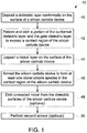
- FIG. 1 illustrates a method 10 whereby an ohmic contact may be formed on a silicon carbide device, in accordance with an embodiment of the present approach.
- FIGS. 2-7 depict an example silicon carbide device 12, a metal-oxide semiconductor field-effect transistor (MOSFET) for power applications, at various stages during the execution of the method 10.
- MOSFET metal-oxide semiconductor field-effect transistor
- FIGS. 2-7 depict an example silicon carbide device 12, a metal-oxide semiconductor field-effect transistor (MOSFET) for power applications, at various stages during the execution of the method 10.
- MOSFET metal-oxide semiconductor field-effect transistor
- JFETs junction-gate field-effect transistors
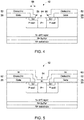
- FIG. 2 illustrates the example silicon carbide device 12 prior to the method 10.
- the basic structure of the MOSFET silicon carbide device 12 illustrated in FIG. 2 includes a substrate body 14 having a substrate layer (e.g., N+ SiC substrate 16) with a number of other layers disposed above, such as the N+ SiC buffer layer 18 and the N- SiC drift layer 20.
- a substrate layer e.g., N+ SiC substrate 16
- the N- SiC drift layer 20 Formed atop the N- SiC drift layer 20 is a P well 22, which includes two heavily-doped N+ regions 24 disposed on opposite sides of a heavily-doped P+ base 26.
- silicon carbide device 12 merely provides an example device structure, and that other silicon carbide device structures (e.g., devices being oppositely doped, devices having additional or fewer layers, devices having structures of different relative dimensions, and so forth) are also presently contemplated.
- a gate e.g., a metallic gate 28
- a relatively thin gate dielectric 30 layer is deposited atop portions of the substrate body 14, separated from the substrate body 14 by a relatively thin gate dielectric 30 layer.
- the method 10 illustrated in FIG. 1 begins with depositing (block 40) a conformal dielectric layer on the surface of a silicon carbide device 12 illustrated in FIG. 2 .
- the resulting structure, illustrated by the silicon carbide device 12 of FIG. 3 includes the conformal dielectric layer 52 deposited over the surface of the silicon carbide device 12.
- the dielectric layer 52 may include silicon dioxide, phospho-silicate glass (PSG), boro-phospho-silicate glass (BPSG), silicon nitride, or any other suitable dielectric material.
- the dielectric layer 52 may be deposited using a chemical vapor deposition (CVD) technique, a spin-coating technique, or another suitable deposition method.
- CVD chemical vapor deposition
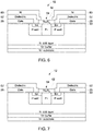
- the method 10 illustrated in FIG. 1 continues with the patterning and etching (block 42) portions of the dielectric layer 52, as well as portions of the gate dielectric layer 30, to expose a contact region of the silicon carbide device 12.
- a portion of the dielectric layer 52 and the gate dielectric layer 30 of the silicon carbide device 12 illustrated in FIG. 3 may be removed to expose a portion of the surface of the substrate body 14.
- FIG. 4 the silicon carbide device 12 of FIG. 3 is illustrated after having a portion of the dielectric layer 52 and the gate dielectric layer 30 removed to expose a contact region 54 at the surface of the substrate body 14.
- the distance 58 may be greater than a distance achievable using self-aligned techniques, as discussed below with regard to FIG. 8 .
- the larger distance 58 provided by the non-self-aligned method 10 may generally allow for minor variations that may be encountered during the patterning and etching of block 42, while still providing a functional device 12.
- the method 10 continues with depositing (block 44) a nickel layer on the surface of the silicon carbide device 12. That is, a nickel layer may be deposited on the surface of the dielectric layer 52 as well as the exposed contact region 54 of the silicon carbide device 12 illustrated in FIG. 4 .
- a nickel layer may be deposited on the surface of the dielectric layer 52 as well as the exposed contact region 54 of the silicon carbide device 12 illustrated in FIG. 4 .
- the silicon carbide device 12 of FIG. 4 is illustrated after having a nickel layer 60 deposited over both the surface of the dielectric layer 52 and the contact region 54.
- the nickel layer 52 may be deposited using a chemical vapor deposition (CVD) technique, sputtering, or another suitable deposition method. Accordingly, after completion of the block 44, the nickel layer 60 illustrated in FIG.
- CVD chemical vapor deposition
- a dielectric surface e.g., the portions of the nickel layer 60 disposed on the dielectric layer 52
- a silicon carbide surface e.g., the portions of the nickel layer 60 disposed on the highly-doped silicon carbide contact region 54.
- RIE reactive ion etching
- back-sputter etching to prepare the surface for metal deposition (e.g., nickel layer 60).
- such aggressive etching techniques are not generally compatible with a lift-off method due to the sensitivity of the exposed photoresist surface.
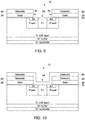
- the method 10 continues with annealing (block 46) the silicon carbide device 12 to form at least one nickel silicide species in the contact region 54 of the silicon carbide device 12. That is, turning to FIG. 6 , the silicon carbide device 12 may be heated such that the portion of the nickel layer 60 (e.g., deposited in block 44) may react with a portion of the silicon carbide contact region 54 to form a nickel silicide layer 62 that includes one or more nickel silicide species.
- the portion of the nickel layer 60 e.g., deposited in block 44
- the silicon carbide device 12 may be heated to between approximately 300 °C and approximately 1100 °C, between approximately 500 °C and approximately 900 °C, or between approximately 600 °C and approximately 800 °C, under a particular atmosphere (e.g., argon, nitrogen, or another suitable atmosphere).
- the anneal of block 46 may provide a nickel silicide layer 62 having a contact resistivity that is approximately four to ten times lower than the contact resistivity of a similarly positioned nickel layer.
- the contact resistivity provided by the nickel silicide layer 62 may be on the order of approximately 10 -3 ohm ⁇ cm 2 to approximately 10 -6 ohm ⁇ cm 2 .
- heating the silicon carbide device 12 during an anneal may cause the formation of one or more nickel silicide species in the nickel silicide layer 62 from the nickel layer 60.
- a continuum of nickel silicide species may exist within the nickel silicide layer 62.
- the nickel silicide layer 62 is formed at a lower annealing temperature (e.g., approximately 300 °C to approximately 500 °C)
- the resulting nickel silicide layer 62 may include a significant amount of Ni 31 Si 12 .
- the ratio of nickel to silicon may range between approximately 2.6 and approximately 1.0.
- the nickel silicide layer 62 is formed at a higher annealing temperature (e.g., approximately 600 °C to approximately 900 °C)
- the resulting nickel silicide layer may including a significant amount of Ni 2 Si.
- the ratio of nickel to silicon may range between approximately 2.6 and approximately 2.0.
- the nickel silicide layer 62 is formed at an even higher annealing temperature (e.g., approximately 900 °C to approximately 1100 °C)
- the resulting nickel silicide layer may including a significant amount of NiSi.
- the ratio of nickel to silicon may range between approximately 2.0 and approximately 1.0. It should further be noted that the remainder of the nickel layer 60 disposed over the dielectric layer 52 may be substantially unaltered during the annealing of block 46 while only the portion of the nickel layer 60 disposed over the contact region 54 may form the nickel silicide layer 62.
- the unreacted nickel layer 60 (e.g., disposed over the dielectric layer 52) may be etched (block 48) from the dielectric surfaces of the silicon carbide device.
- the nickel silicide layer 62 having a different reactivity than the unreacted nickel layer 60, may remain substantially unaltered.
- the silicon carbide device 12 is illustrated after the unreacted nickel layer 60 has been etched such that only the nickel silicide layer 62 remains.
- the unreacted nickel layer 60 may be removed using a wet-etching technique.
- the etching of the unreacted nickel layer 60 set forth in block 48 may not be performed such that the final device structure includes the unreacted nickel layer 60, in addition to the nickel silicide layer 62. It should be appreciated that in such embodiments, adequate care may be taken to avoid contacting the nickel layer 60 with certain other device features, such as the gate contact pad (not shown).
- the silicon carbide device 12 maybe annealed (block 50) a second time, at a higher temperature than the first anneal, to further improve the contact resistance at the nickel silicide layer 62.
- the silicon carbide device 12 may be heated to between approximately 800 °C to approximately 1100 °C under a particular atmosphere (e.g., argon, nitrogen, or another suitable atmosphere).
- a particular atmosphere e.g., argon, nitrogen, or another suitable atmosphere.
- heating the silicon carbide device 12 to a higher temperature e.g., during the second anneal set forth in block 50
- the nickel silicide layer 62 may be richer in certain nickel silicide species (e.g., Ni 2 Si, NiSi, etc.).
- the ratio of nickel to silicon in the nickel silicide layer 62 may approach approximately 1. It should further be appreciated that the nickel silicide layer 62 formed by the second anneal of block 50 may further reduce the contact resistance at the contact region 54 of the silicon carbide device 12.
- FIG. 8 illustrates a second method 70 whereby a self-aligned ohmic contact (e.g., for a contact via) may be formed on a silicon carbide device 12, in accordance with another embodiment of the present approach.
- FIGS. 2 and 9-14 depict the same example MOSFET silicon carbide device 12 discussed above, at various stages during the execution of the method 70 illustrated in FIG. 8 .
- the discussion of the second method 70 may be directed to the silicon carbide MOSFET 12, the present technique may be applicable to any MOSFET or other suitable silicon carbide devices.
- FIG. 2 which is described above, illustrates an example silicon carbide device 12 prior to the execution of the method 70 illustrated in FIG. 8 .
- the method 70 illustrated in FIG. 8 begins with depositing (block 72) a dielectric layer on the surface of a silicon carbide device 12 illustrated in FIG. 2 , followed by patterning and etching the deposited dielectric film, as well as the gate electrode, to form a co-incident edge.
- the resulting structure, illustrated by the silicon carbide device 12 illustrated in FIG. 9 . includes a dielectric layer 90 (e.g., including silicon dioxide, phospho-silicate glass, boro-phospho-silicate glass, silicon nitride, or any other suitable dielectric material) disposed over the gate 28. Additionally, the dielectric layer 90 may be deposited using CVD, spin-coating, or another suitable deposition technique. Further, the dielectric layer 90 illustrated in FIG. 9 has been patterned and etched (e.g., using photolithographic techniques) to expose the contact region 54 of the silicon carbide device 12 and to provide a coincident edge 92.
- a dielectric layer 90 e.g., including silicon dioxide, phospho
- the method 70 illustrated in FIG. 8 continues with the deposition (block 74) of another dielectric layer conformably on the surface of the silicon carbide device 12.
- the silicon carbide device 12 is illustrated after the conformal deposition of the dielectric layer 94.
- the dielectric layer 94 may include silicon dioxide, phospho-silicate glass (PSG), boro-phospho-silicate glass (BPSG), silicon nitride, or any other suitable dielectric material. Additionally, the dielectric layer 94 may be deposited using CVD, spin-coating, or another suitable deposition technique.
- the method 70 continues with blanket etching (block 76) of the conformal dielectric layer deposited in block 74 to create a dielectric spacer between the gate 30 and the contact region 54.
- the silicon carbide device 12 is illustrated after the blanket etching (e.g., as set forth in block 76) of the dielectric layer 94 deposited in block 74.
- the blanket etching removes most of the dielectric layer 94, exposing the contact region 54, but leaving behind a spacer 96 disposed between the gate 28 and the contact region 54 of the silicon carbide device 12. It should be appreciated that, by controlling the thickness of the dielectric layer 94 deposited in block 74 and the blanket etching conditions of block 76, the width 98 of the dielectric spacer 96 may be controlled.
- the method 70 of FIG. 8 continues with the deposition (block 78) of a nickel layer over the surface of the silicon carbide device.
- a nickel layer over the surface of the silicon carbide device.
- the silicon carbide device 12 is illustrated having the nickel layer 60 disposed over the surface of the silicon carbide device, including the surfaces of the remaining dielectric layer 90, the exposed contact region 54, and the dielectric spacer 96.
- the nickel layer 52 may be deposited using a chemical vapor deposition (CVD) technique, sputtering, or another suitable deposition method.
- CVD chemical vapor deposition
- the silicon carbide device 12 maybe annealed (block 80) such that at least one nickel silicide species is formed in the contact region 54 of the silicon carbide device.
- the silicon carbide device 12 is illustrated after having been annealed such that a nickel silicide layer 62 is formed from the portion of the nickel layer 60 deposited over the contact region 54.
- the silicon carbide device 12 may be heated to between approximately 300 °C and approximately 1100 °C, between approximately 500 °C and approximately 900 °C, or between approximately 600 °C and approximately 800 °C, under a particular atmosphere (e.g., argon, nitrogen, or another suitable atmosphere).
- the anneal of block 80 may provide a nickel silicide layer 62 having a contact resistivity that is approximately four to ten times lower than the contact resistivity of a similarly positioned nickel layer.
- the contact resistivity provided by the nickel silicide layer 62 may be on the order of approximately 10 -3 to approximately 10 -6 ohm ⁇ cm 2 .
- heating the silicon carbide device 12 during an anneal may cause the formation of one or more nickel silicide species in the nickel silicide layer 62 from the nickel layer 60.
- the nickel silicide layer 62 may include a significant amount of Ni 31 Si 12 . Accordingly, for such a nickel silicide layer 62, the ratio of nickel to silicon may range between approximately 2.6 and approximately 1.0.
- the resulting nickel silicide layer may including a significant amount of Ni 2 Si. Accordingly, for such a nickel silicide layer 62, the ratio of nickel to silicon may range between approximately 2.6 and approximately 2.0.
- the nickel silicide layer 62 is formed at an even higher annealing temperature (e.g., approximately 900 °C to approximately 1100 °C)
- the resulting nickel silicide layer may including a significant amount of NiSi. Accordingly, for such a nickel silicide layer 62, the ratio of nickel to silicon may range between approximately 2.0 and approximately 1.0.
- the remainder of the nickel layer 60 disposed over the dielectric layer 90 and/or the dielectric spacer 96 may be substantially unaltered during the annealing of block 46 while only the portion of the nickel layer 60 disposed over the contact region 54 may form the nickel silicide layer 62.
- the unreacted portions of the nickel layer 60 may be etched (block 82) from the dielectric surfaces (e.g., the dielectric layer 90 and the dielectric spacer 96) while leaving the nickel silicide layer 62 substantially unaffected.
- the silicon carbide device 12 is illustrated after the unreacted nickel layer 60 has been removed (e.g., using a wet etching technique), leaving behind only the nickel silicide layer 62.
- the nickel silicide layer 62 is self-aligned relative to the gate 28 and/or the contact region 54 by the spacer 96.
- the width 98 of the dielectric spacer 96 may generally be less than the spacing between the gate and the nickel silicide layer that may be achieved using other alignment methods (e.g., less than the width 58 illustrated in FIG. 4 for the non-self-aligned method 10 illustrated in FIG. 1 ). It should be appreciated that, in other embodiments, the etching of the unreacted nickel layer 60 set forth in block 82 may not be performed such that the final device structure includes the unreacted nickel layer 60, in addition to the nickel silicide layer 62. It should be appreciated that in such embodiments, adequate care may be taken to avoid contacting the nickel layer 60 with certain other device features, such as the gate contact pad (not shown).
- the method 70 continues with a second anneal being performed (block 84) on the silicon carbide device 12. That is, after the unreacted nickel layer 60 has been removed as set forth in block 82, the silicon carbide device 12 illustrated in FIG. 14 may be annealed a second time, at a higher temperature than the first anneal set forth in block 80.
- the silicon carbide device 12 may be heated to between approximately 800 °C to approximately 1100 °C under a particular atmosphere (e.g., argon, nitrogen, or another suitable atmosphere).
- heating the silicon carbide device 12 to a higher temperature may cause the nickel silicide layer 62 that is formed during the first anneal (e.g., set forth in block 80) to further react with the silicon carbide contact region 54 to form other nickel silicide species (e.g., Ni 2 Si, NiSi, etc.), in which the ratio of nickel to silicon in the nickel silicide layer 62 may approach approximately 1.0.
- the nickel silicide layer 62 formed by the second anneal of block 80 may further reduce the contact resistance at the contact region 54 of the silicon carbide device 12.
- FIG. 15 illustrates an alternative embodiment of a non-self-aligned silicon carbide device 12 that includes a titanium/aluminum layer 100 disposed over a portion of the contact region 54. More specifically, the titanium/aluminum layer 100 is disposed on the P+ base 32 of the silicon carbide device 12, while a nickel silicide 102 is disposed over the remainder of the contact region 54. Furthermore, the portion of the nickel layer 104 remains disposed over the titanium/aluminum layer 100.
- the silicon carbide device 12 illustrated in FIG. 15 may be manufactured using a non-self-aligned method (e.g., similar to the method 10 illustrated in FIG. 1 ), but including steps to selectively deposit the titanium/aluminum layer 100 in the middle of the contact region 54 prior to the deposition of the nickel layer (e.g., between blocks 42 and 44 of the method 10 illustrated in FIG. 1 ).
- FIG. 16 illustrates an alternative embodiment of a self-aligned silicon carbide device 12 that also includes the titanium/aluminum layer 100 disposed over a portion of the contact region 54.
- the silicon carbide device 12 illustrated in FIG. 16 includes a titanium/aluminum layer 100 disposed over the P+ base 32 of the silicon carbide device 12, while nickel silicide 102 is disposed over the remainder of the contact region 54.
- a portion of the nickel layer 104 remains disposed over the titanium/aluminum layer 100.
- the silicon carbide device 12 illustrated in FIG. 16 may be manufactured using a self-aligned method (e.g., like the method 70 illustrated in FIG. 8 ), but including steps to selectively deposit the titanium/aluminum layer 100 in the middle of the contact region 54 prior to the deposition of the nickel layer (e.g., between blocks 76 and 78 of the method 70 illustrated in FIG. 8 ).
- Beneficial effects of the presently disclosed technique include the facile formation of an ohmic contact for a silicon carbide device. That is, the present technique enables only portions of the nickel layer deposited on a silicon carbide surface to be converted to the nickel silicide under annealing conditions to provide the ohmic contact (e.g., in the contact region of a silicon carbide field-effect transistor (FET) device). Further, since the conditions of the anneal do not provoke portions of the nickel layer deposited on a dielectric surface to react or form nickel silicide, these unreacted portions of the deposited nickel layer may be easily and selectively removed (e.g., via wet etching) such that only the nickel silicide remains in the contact region of the silicon carbide device.
- FET silicon carbide field-effect transistor
- the present technique may be applied to methods for constructing both non-self-aligned (e.g., according to the method 10 of FIG. 1 ) and self-aligned (e.g., according to the method 70 of FIG. 8 ) silicon carbide devices that include the nickel silicide ohmic contact. It should further be appreciated that using the disclosed approach with a self-aligning technique (e.g., as set forth in the method 70 of FIG. 8 ) may enable higher device densities (e.g., smaller cell pitches) and improved device yields. Furthermore, the present technique may be applied to methods for constructing silicon carbide devices that include other metal layers (e.g., the titanium/aluminum layer 100 illustrated in FIGS. 15 and 16 ) in addition to having nickel silicide disposed in the contact region of the silicon carbide device to provide an ohmic contact.
- other metal layers e.g., the titanium/aluminum layer 100 illustrated in FIGS. 15 and 16
Claims (15)
- Dispositif au carbure de silicium (12) comprenant :une électrode de grille (28) disposée sur une portion d'un substrat de carbure de silicium (14) ;un film diélectrique (52) disposé sur l'électrode de grille ;une région de contact (54) du dispositif au carbure de silicium disposée près de l'électrode de grille, la région de contact (54) incluant une base (26) d'un puits (22) du substrat de carbure de silicium (14), la base (26) du puits (22) étant dopée avec un premier type de connectivité, et deux régions (24) sur des côtés opposés de la base (26) du puits (22), les deux régions (24) étant dopées avec un deuxième type de connectivité opposé au premier type de connectivité ; etune pluralité de couches (62, 100, 102) disposées sur la région de contact du dispositif au carbure de silicium, dans lequel la pluralité de couches sont configurées pour fournir un contact ohmique à la région de contact du dispositif au carbure de silicium, dans lequel la pluralité de couches s'étendent sur une totalité d'une surface supérieure de la base (26) du puits (22) et sont en contact direct avec la surface supérieure de la base (26) du puits (22) et en travers d'au moins des portions de chacune des deux régions (24) sur des côtés opposés de la base (26) du puits (22), dans lequel la pluralité de couches comprennent une couche de titane/aluminium (100) disposée sur une première portion de la base du puits de la région de contact (54) du dispositif au carbure de silicium ; et dans lequel la pluralité de couches comprennent en outre des couches de siliciure de nickel (102) disposées sur des portions des deux régions et étant en contact direct avec une surface supérieure d'une deuxième portion de la base (26) du puits (22) de la région de contact (54) du dispositif au carbure de silicium.
- Dispositif selon la revendication 1, comprenant une couche de nickel (104) disposée sur la couche de titane/aluminium.
- Dispositif selon la revendication 1, dans lequel la région de contact (54) du dispositif au carbure de silicium est configurée pour être espacée d'une distance de l'électrode de grille (28).
- Dispositif selon la revendication 3, comprenant un élément d'écartement diélectrique (96) disposé entre l'électrode de grille (28) et la région de contact (54) du dispositif au carbure de silicium, dans lequel l'élément d'écartement diélectrique (96) est configuré pour aligner automatiquement la région de contact (54) du dispositif au carbure de silicium par rapport à l'électrode de grille (28).
- Dispositif selon la revendication 4, dans lequel l'élément d'écartement diélectrique (96) est configuré pour aligner automatiquement un trou d'interconnexion de contact par rapport à la région de contact (54) du dispositif au carbure de silicium.
- Dispositif selon la revendication 1, dans lequel un rapport nickel/silicium de la couche de siliciure de nickel est compris entre 2,6 et 1,0.
- Dispositif selon la revendication 6, dans lequel le rapport nickel/silicium de la couche de siliciure de nickel est compris entre 2,6 et 2,0.
- Dispositif selon la revendication 6, dans lequel le rapport nickel/silicium de la couche de siliciure de nickel est compris entre 2,0 et 1,0.
- Dispositif selon la revendication 1, dans lequel le dispositif au carbure de silicium est un transistor à effet de champ à semi-conducteur à oxydes métalliques au carbure de silicium (MOSFET).
- Procédé (10, 70) comprenant :la formation d'un dispositif au carbure de silicium (12), le dispositif au carbure de silicium comprenant une électrode de grille (28) disposée sur une portion d'un substrat de carbure de silicium (14), le dépôt d'un film diélectrique comprenant le dépôt d'une première couche diélectrique (90) et d'une deuxième couche diélectrique (94) disposées sur l'électrode de grille (28), et la formation d'une région de contact (54) du dispositif au carbure de silicium près de l'électrode de grille (28), la région de contact (54) du dispositif au carbure de silicium comprenant une base (26) d'un puits (22) du substrat de carbure de silicium (14), la base du puits étant dopée avec un premier type de connectivité, et la formation deux régions (24) sur des côtés opposés de la base du puits, les deux régions (24) étant dopées avec un deuxième type de connectivité opposé au premier type de connectivité, dans lequel une surface du dispositif au carbure de silicium comprend une surface supérieure de la région de contact du dispositif au carbure de silicium ; et la gravure de la deuxième couche diélectrique (94) pour exposer la région de contact (54) du dispositif au carbure de silicium tout en fournissant un élément d'écartement diélectrique entre l'électrode de grille et la région de contact du dispositif au carbure de silicium ; le dépôt d'une couche de titane/aluminium (100) au milieu de la région de contact (54) ; et le dépôt (40) d'une couche de nickel (80) sur la surface d'un dispositif au carbure de silicium (12) et sur la couche de titane/aluminium (100) ; etle recuit (46) du dispositif au carbure de silicium pour convertir une portion de la couche de nickel (80) en une couche de siliciure de nickel (62) comprenant au moins une espèce de siliciure de nickel, dans lequel la couche de siliciure de nickel (62) est configurée pour fournir un contact à faible résistance dans la région de contact du dispositif au carbure de silicium et s'étend sur une totalité d'une surface supérieure de la base (26) du puits (22) et est en contact direct avec la surface supérieure de la base (26) du puits (22) et en travers d'au moins des portions de chacune des deux régions (24) sur des côtés opposés de la base (26) du puits (22).
- Procédé selon la revendication 10, dans lequel le contact à faible résistance comprend une résistivité de contact inférieure à 10-5 ohm.cm2.
- Procédé selon la revendication 10, dans lequel le contact à faible résistance comprend une résistivité de contact 4 à 10 fois inférieure à la couche de nickel avant le recuit.
- Procédé selon la revendication 10, comprenant le dépôt d'une couche diélectrique de grille sur la surface du dispositif au carbure de silicium.
- Procédé selon la revendication 13, comprenant le dépôt de la première couche diélectrique sur la couche diélectrique de grille et l'électrode de grille ; le modelage et la gravure de la première couche diélectrique et de la couche d'électrode de grille pour former un bord coïncident et exposer la région de contact ; le dépôt de la deuxième couche diélectrique de manière conforme sur la surface du dispositif au carbure de silicium.
- Procédé selon la revendication 14, dans lequel l'élément d'écartement diélectrique est configuré pour aligner automatiquement la couche de siliciure de nickel par rapport à l'électrode de grille et par rapport à la région de contact du dispositif au carbure de silicium.
Applications Claiming Priority (1)
| Application Number | Priority Date | Filing Date | Title |
|---|---|---|---|
| US13/718,031 US9230807B2 (en) | 2012-12-18 | 2012-12-18 | Systems and methods for ohmic contacts in silicon carbide devices |
Publications (3)
| Publication Number | Publication Date |
|---|---|
| EP2747147A2 EP2747147A2 (fr) | 2014-06-25 |
| EP2747147A3 EP2747147A3 (fr) | 2017-08-02 |
| EP2747147B1 true EP2747147B1 (fr) | 2019-02-06 |
Family
ID=49378169
Family Applications (1)
| Application Number | Title | Priority Date | Filing Date |
|---|---|---|---|
| EP13189168.1A Active EP2747147B1 (fr) | 2012-12-18 | 2013-10-17 | Systèmes et procédés pour contacts ohmiques dans des dispositifs en carbure de silicium |
Country Status (6)
| Country | Link |
|---|---|
| US (2) | US9230807B2 (fr) |
| EP (1) | EP2747147B1 (fr) |
| JP (2) | JP6642931B2 (fr) |
| CN (1) | CN103872103B (fr) |
| BR (1) | BR102013026784A2 (fr) |
| CA (1) | CA2829245C (fr) |
Families Citing this family (12)
| Publication number | Priority date | Publication date | Assignee | Title |
|---|---|---|---|---|
| US9425153B2 (en) | 2013-04-04 | 2016-08-23 | Monolith Semiconductor Inc. | Semiconductor devices comprising getter layers and methods of making and using the same |
| JP2016046309A (ja) * | 2014-08-20 | 2016-04-04 | 住友電気工業株式会社 | 炭化珪素半導体装置の製造方法 |
| WO2017041268A1 (fr) * | 2015-09-10 | 2017-03-16 | 中国科学院微电子研究所 | Dispositif mosfet au carbure de silicium et son procédé de fabrication |
| US9666482B1 (en) * | 2016-09-14 | 2017-05-30 | Infineon Technologies Ag | Self aligned silicon carbide contact formation using protective layer |
| US10607841B2 (en) * | 2017-12-17 | 2020-03-31 | Applied Materials, Inc. | Silicide films through selective deposition |
| US10629686B2 (en) * | 2018-08-02 | 2020-04-21 | Semiconductor Components Industries, Llc | Carbon-controlled ohmic contact layer for backside ohmic contact on a silicon carbide power semiconductor device |
| EP3660885B1 (fr) * | 2018-11-28 | 2023-05-24 | Infineon Technologies AG | Dispositif de nitrure du groupe iii et procédé de fabrication d'un contact ohmique pour un dispositif à base de nitrure de groupe iii |
| CN109979813B (zh) * | 2019-03-28 | 2020-12-11 | 厦门市三安集成电路有限公司 | 一种低温碳化硅欧姆接触的制备方法及金属结构 |
| US11075277B2 (en) * | 2019-06-04 | 2021-07-27 | Genesic Semiconductor Inc. | Manufacture of self-aligned power devices |
| JP7354028B2 (ja) * | 2020-03-13 | 2023-10-02 | 株式会社東芝 | 半導体装置、半導体装置の製造方法、インバータ回路、駆動装置、車両、及び、昇降機 |
| JP7354027B2 (ja) * | 2020-03-13 | 2023-10-02 | 株式会社東芝 | 半導体装置、半導体装置の製造方法、インバータ回路、駆動装置、車両、及び、昇降機 |
| CN117238969A (zh) * | 2023-11-13 | 2023-12-15 | 深圳基本半导体有限公司 | 碳化硅mosfet器件及其制备方法与应用 |
Family Cites Families (28)
| Publication number | Priority date | Publication date | Assignee | Title |
|---|---|---|---|---|
| FR2542920B1 (fr) | 1983-03-18 | 1986-06-06 | Commissariat Energie Atomique | Procede de positionnement d'une ligne d'interconnexion sur un trou de contact electrique d'un circuit integre |
| JPH0864801A (ja) * | 1994-08-26 | 1996-03-08 | Fuji Electric Co Ltd | 炭化けい素半導体素子およびその製造方法 |
| US5510281A (en) | 1995-03-20 | 1996-04-23 | General Electric Company | Method of fabricating a self-aligned DMOS transistor device using SiC and spacers |
| JPH10125620A (ja) | 1996-10-17 | 1998-05-15 | Denso Corp | 炭化珪素半導体装置 |
| US6043126A (en) * | 1996-10-25 | 2000-03-28 | International Rectifier Corporation | Process for manufacture of MOS gated device with self aligned cells |
| JP3703643B2 (ja) * | 1998-12-25 | 2005-10-05 | 三菱電機株式会社 | 半導体装置およびその製造方法 |
| JP4876321B2 (ja) * | 2001-03-30 | 2012-02-15 | 株式会社デンソー | 炭化珪素半導体装置の製造方法 |
| US7297626B1 (en) * | 2001-08-27 | 2007-11-20 | United States Of America As Represented By The Secretary Of The Army | Process for nickel silicide Ohmic contacts to n-SiC |
| US8133789B1 (en) * | 2003-04-11 | 2012-03-13 | Purdue Research Foundation | Short-channel silicon carbide power mosfet |
| JP4230869B2 (ja) * | 2003-09-25 | 2009-02-25 | 株式会社東芝 | 高耐圧半導体装置 |
| JP2005276978A (ja) * | 2004-03-24 | 2005-10-06 | Nissan Motor Co Ltd | オーミック電極構造体の製造方法、オーミック電極構造体、半導体装置の製造方法および半導体装置 |
| US20060006393A1 (en) * | 2004-07-06 | 2006-01-12 | Ward Allan Iii | Silicon-rich nickel-silicide ohmic contacts for SiC semiconductor devices |
| GB2424312B (en) | 2005-03-14 | 2010-03-03 | Denso Corp | Method of forming an ohmic contact in wide band semiconductor |
| US8377812B2 (en) | 2006-11-06 | 2013-02-19 | General Electric Company | SiC MOSFETs and self-aligned fabrication methods thereof |
| US20080108190A1 (en) | 2006-11-06 | 2008-05-08 | General Electric Company | SiC MOSFETs and self-aligned fabrication methods thereof |
| JP4939960B2 (ja) * | 2007-02-05 | 2012-05-30 | 株式会社東芝 | 半導体装置およびその製造方法 |
| JP4539684B2 (ja) * | 2007-06-21 | 2010-09-08 | 株式会社デンソー | 炭化珪素半導体装置およびその製造方法 |
| JP2009019837A (ja) * | 2007-07-13 | 2009-01-29 | Tlv Co Ltd | 廃蒸気回収装置 |
| JP4365894B2 (ja) * | 2007-08-07 | 2009-11-18 | パナソニック株式会社 | 炭化珪素半導体素子の製造方法 |
| JP2009043880A (ja) * | 2007-08-08 | 2009-02-26 | Panasonic Corp | 炭化珪素半導体装置の製造方法および炭化珪素半導体装置 |
| JP2009194216A (ja) * | 2008-02-15 | 2009-08-27 | Hitachi Ltd | 半導体装置の製造方法 |
| KR20100123589A (ko) * | 2008-02-22 | 2010-11-24 | 스미토모덴키고교가부시키가이샤 | 반도체 장치 및 반도체 장치의 제조 방법 |
| CN102007595B (zh) * | 2008-04-15 | 2013-12-25 | 住友电气工业株式会社 | 半导体器件及其制造方法 |
| US8035112B1 (en) * | 2008-04-23 | 2011-10-11 | Purdue Research Foundation | SIC power DMOSFET with self-aligned source contact |
| US8188482B2 (en) | 2008-12-22 | 2012-05-29 | Infineon Technologies Austria Ag | SiC semiconductor device with self-aligned contacts, integrated circuit and manufacturing method |
| JP2012094555A (ja) * | 2009-02-18 | 2012-05-17 | Mitsubishi Electric Corp | 半導体装置の製造方法 |
| WO2011027540A1 (fr) * | 2009-09-02 | 2011-03-10 | パナソニック株式会社 | Elément semi-conducteur et procédé de fabrication associé |
| JP5777455B2 (ja) * | 2011-09-08 | 2015-09-09 | 株式会社東芝 | 半導体装置および半導体装置の製造方法 |
-
2012
- 2012-12-18 US US13/718,031 patent/US9230807B2/en active Active
-
2013
- 2013-10-03 CA CA2829245A patent/CA2829245C/fr active Active
- 2013-10-15 JP JP2013214306A patent/JP6642931B2/ja active Active
- 2013-10-17 BR BRBR102013026784-8A patent/BR102013026784A2/pt not_active Application Discontinuation
- 2013-10-17 EP EP13189168.1A patent/EP2747147B1/fr active Active
- 2013-10-18 CN CN201310726139.XA patent/CN103872103B/zh active Active
-
2016
- 2016-01-04 US US14/986,922 patent/US9601332B2/en active Active
-
2017
- 2017-12-18 JP JP2017241267A patent/JP6537082B2/ja active Active
Non-Patent Citations (1)
| Title |
|---|
| None * |
Also Published As
| Publication number | Publication date |
|---|---|
| BR102013026784A2 (pt) | 2014-09-16 |
| US9230807B2 (en) | 2016-01-05 |
| CA2829245C (fr) | 2020-09-22 |
| CA2829245A1 (fr) | 2014-06-18 |
| EP2747147A3 (fr) | 2017-08-02 |
| JP2018082190A (ja) | 2018-05-24 |
| US9601332B2 (en) | 2017-03-21 |
| US20140167068A1 (en) | 2014-06-19 |
| JP6642931B2 (ja) | 2020-02-12 |
| JP6537082B2 (ja) | 2019-07-03 |
| CN103872103B (zh) | 2019-08-20 |
| EP2747147A2 (fr) | 2014-06-25 |
| US20160118258A1 (en) | 2016-04-28 |
| JP2014120758A (ja) | 2014-06-30 |
| CN103872103A (zh) | 2014-06-18 |
Similar Documents
| Publication | Publication Date | Title |
|---|---|---|
| EP2747147B1 (fr) | Systèmes et procédés pour contacts ohmiques dans des dispositifs en carbure de silicium | |
| CN104425367B (zh) | 硅化物形成中的双层金属沉积 | |
| US9024330B2 (en) | Semiconductor device and manufacturing method thereof | |
| JPS5950567A (ja) | 電界効果トランジスタの製造方法 | |
| US9704743B2 (en) | Method for manufacturing silicon carbide semiconductor device | |
| CN113594038B (zh) | 一种半导体器件制备方法 | |
| JP2019212902A (ja) | 炭化ケイ素体を有する半導体デバイスおよび製造方法 | |
| CN103094330B (zh) | 半导体器件及其制造方法 | |
| CN102822976A (zh) | 用于场效应晶体管器件的自动对准接触 | |
| US11728389B2 (en) | Group III nitride device having an ohmic contact | |
| JP6376736B2 (ja) | 半導体デバイスおよびその製造方法 | |
| TW200418128A (en) | High density trench power MOSFET structure and method thereof | |
| CN114496764B (zh) | 一种半导体器件及其制备方法 | |
| JP7070392B2 (ja) | 半導体装置の製造方法 | |
| CN112838121B (zh) | 环栅全控型AlGaN/GaN毫米波HEMT器件及其制备方法 | |
| CN112259607A (zh) | 氮化镓半导体器件及其制备方法 | |
| CN103377894A (zh) | 金属硅化物制造方法 | |
| CN113871464A (zh) | 硅终端金刚石场效应晶体管及其制备方法 | |
| JPH0324733A (ja) | 半導体装置及びその製造方法 | |
| JPS60226180A (ja) | 半導体装置及びその製造方法 | |
| JP2019083293A (ja) | 半導体装置とその製造方法 | |
| JPS6151979A (ja) | 半導体装置の製造方法 | |
| KR20100063336A (ko) | 실리콘 카바이드 반도체 소자의 제작 방법 | |
| JPS62293778A (ja) | 半導体装置の製造方法 |
Legal Events
| Date | Code | Title | Description |
|---|---|---|---|
| PUAI | Public reference made under article 153(3) epc to a published international application that has entered the european phase |
Free format text: ORIGINAL CODE: 0009012 |
|
| 17P | Request for examination filed |
Effective date: 20131017 |
|
| AK | Designated contracting states |
Kind code of ref document: A2 Designated state(s): AL AT BE BG CH CY CZ DE DK EE ES FI FR GB GR HR HU IE IS IT LI LT LU LV MC MK MT NL NO PL PT RO RS SE SI SK SM TR |
|
| AX | Request for extension of the european patent |
Extension state: BA ME |
|
| PUAL | Search report despatched |
Free format text: ORIGINAL CODE: 0009013 |
|
| AK | Designated contracting states |
Kind code of ref document: A3 Designated state(s): AL AT BE BG CH CY CZ DE DK EE ES FI FR GB GR HR HU IE IS IT LI LT LU LV MC MK MT NL NO PL PT RO RS SE SI SK SM TR |
|
| AX | Request for extension of the european patent |
Extension state: BA ME |
|
| RIC1 | Information provided on ipc code assigned before grant |
Ipc: H01L 21/336 20060101ALI20170627BHEP Ipc: H01L 29/78 20060101AFI20170627BHEP Ipc: H01L 29/45 20060101ALI20170627BHEP Ipc: H01L 21/28 20060101ALI20170627BHEP Ipc: H01L 29/16 20060101ALN20170627BHEP |
|
| STAA | Information on the status of an ep patent application or granted ep patent |
Free format text: STATUS: REQUEST FOR EXAMINATION WAS MADE |
|
| R17P | Request for examination filed (corrected) |
Effective date: 20180202 |
|
| RBV | Designated contracting states (corrected) |
Designated state(s): AL AT BE BG CH CY CZ DE DK EE ES FI FR GB GR HR HU IE IS IT LI LT LU LV MC MK MT NL NO PL PT RO RS SE SI SK SM TR |
|
| RIC1 | Information provided on ipc code assigned before grant |
Ipc: H01L 29/45 20060101ALI20180906BHEP Ipc: H01L 21/336 20060101ALI20180906BHEP Ipc: H01L 21/28 20060101ALI20180906BHEP Ipc: H01L 29/78 20060101AFI20180906BHEP Ipc: H01L 29/16 20060101ALN20180906BHEP |
|
| GRAP | Despatch of communication of intention to grant a patent |
Free format text: ORIGINAL CODE: EPIDOSNIGR1 |
|
| STAA | Information on the status of an ep patent application or granted ep patent |
Free format text: STATUS: GRANT OF PATENT IS INTENDED |
|
| RIC1 | Information provided on ipc code assigned before grant |
Ipc: H01L 29/16 20060101ALN20180911BHEP Ipc: H01L 29/45 20060101ALI20180911BHEP Ipc: H01L 21/336 20060101ALI20180911BHEP Ipc: H01L 21/28 20060101ALI20180911BHEP Ipc: H01L 29/78 20060101AFI20180911BHEP |
|
| RIC1 | Information provided on ipc code assigned before grant |
Ipc: H01L 21/28 20060101ALI20180918BHEP Ipc: H01L 29/78 20060101AFI20180918BHEP Ipc: H01L 29/16 20060101ALN20180918BHEP Ipc: H01L 29/45 20060101ALI20180918BHEP Ipc: H01L 21/336 20060101ALI20180918BHEP |
|
| INTG | Intention to grant announced |
Effective date: 20181012 |
|
| GRAS | Grant fee paid |
Free format text: ORIGINAL CODE: EPIDOSNIGR3 |
|
| GRAA | (expected) grant |
Free format text: ORIGINAL CODE: 0009210 |
|
| STAA | Information on the status of an ep patent application or granted ep patent |
Free format text: STATUS: THE PATENT HAS BEEN GRANTED |
|
| AK | Designated contracting states |
Kind code of ref document: B1 Designated state(s): AL AT BE BG CH CY CZ DE DK EE ES FI FR GB GR HR HU IE IS IT LI LT LU LV MC MK MT NL NO PL PT RO RS SE SI SK SM TR |
|
| REG | Reference to a national code |
Ref country code: GB Ref legal event code: FG4D |
|
| REG | Reference to a national code |
Ref country code: CH Ref legal event code: EP Ref country code: AT Ref legal event code: REF Ref document number: 1095426 Country of ref document: AT Kind code of ref document: T Effective date: 20190215 |
|
| REG | Reference to a national code |
Ref country code: IE Ref legal event code: FG4D |
|
| REG | Reference to a national code |
Ref country code: DE Ref legal event code: R096 Ref document number: 602013050446 Country of ref document: DE |
|
| REG | Reference to a national code |
Ref country code: NL Ref legal event code: MP Effective date: 20190206 |
|
| REG | Reference to a national code |
Ref country code: LT Ref legal event code: MG4D |
|
| PG25 | Lapsed in a contracting state [announced via postgrant information from national office to epo] |
Ref country code: PT Free format text: LAPSE BECAUSE OF FAILURE TO SUBMIT A TRANSLATION OF THE DESCRIPTION OR TO PAY THE FEE WITHIN THE PRESCRIBED TIME-LIMIT Effective date: 20190606 Ref country code: NL Free format text: LAPSE BECAUSE OF FAILURE TO SUBMIT A TRANSLATION OF THE DESCRIPTION OR TO PAY THE FEE WITHIN THE PRESCRIBED TIME-LIMIT Effective date: 20190206 Ref country code: LT Free format text: LAPSE BECAUSE OF FAILURE TO SUBMIT A TRANSLATION OF THE DESCRIPTION OR TO PAY THE FEE WITHIN THE PRESCRIBED TIME-LIMIT Effective date: 20190206 Ref country code: NO Free format text: LAPSE BECAUSE OF FAILURE TO SUBMIT A TRANSLATION OF THE DESCRIPTION OR TO PAY THE FEE WITHIN THE PRESCRIBED TIME-LIMIT Effective date: 20190506 Ref country code: SE Free format text: LAPSE BECAUSE OF FAILURE TO SUBMIT A TRANSLATION OF THE DESCRIPTION OR TO PAY THE FEE WITHIN THE PRESCRIBED TIME-LIMIT Effective date: 20190206 Ref country code: FI Free format text: LAPSE BECAUSE OF FAILURE TO SUBMIT A TRANSLATION OF THE DESCRIPTION OR TO PAY THE FEE WITHIN THE PRESCRIBED TIME-LIMIT Effective date: 20190206 |
|
| REG | Reference to a national code |
Ref country code: AT Ref legal event code: MK05 Ref document number: 1095426 Country of ref document: AT Kind code of ref document: T Effective date: 20190206 |
|
| PG25 | Lapsed in a contracting state [announced via postgrant information from national office to epo] |
Ref country code: GR Free format text: LAPSE BECAUSE OF FAILURE TO SUBMIT A TRANSLATION OF THE DESCRIPTION OR TO PAY THE FEE WITHIN THE PRESCRIBED TIME-LIMIT Effective date: 20190507 Ref country code: IS Free format text: LAPSE BECAUSE OF FAILURE TO SUBMIT A TRANSLATION OF THE DESCRIPTION OR TO PAY THE FEE WITHIN THE PRESCRIBED TIME-LIMIT Effective date: 20190606 Ref country code: BG Free format text: LAPSE BECAUSE OF FAILURE TO SUBMIT A TRANSLATION OF THE DESCRIPTION OR TO PAY THE FEE WITHIN THE PRESCRIBED TIME-LIMIT Effective date: 20190506 Ref country code: RS Free format text: LAPSE BECAUSE OF FAILURE TO SUBMIT A TRANSLATION OF THE DESCRIPTION OR TO PAY THE FEE WITHIN THE PRESCRIBED TIME-LIMIT Effective date: 20190206 Ref country code: LV Free format text: LAPSE BECAUSE OF FAILURE TO SUBMIT A TRANSLATION OF THE DESCRIPTION OR TO PAY THE FEE WITHIN THE PRESCRIBED TIME-LIMIT Effective date: 20190206 Ref country code: HR Free format text: LAPSE BECAUSE OF FAILURE TO SUBMIT A TRANSLATION OF THE DESCRIPTION OR TO PAY THE FEE WITHIN THE PRESCRIBED TIME-LIMIT Effective date: 20190206 |
|
| PG25 | Lapsed in a contracting state [announced via postgrant information from national office to epo] |
Ref country code: SK Free format text: LAPSE BECAUSE OF FAILURE TO SUBMIT A TRANSLATION OF THE DESCRIPTION OR TO PAY THE FEE WITHIN THE PRESCRIBED TIME-LIMIT Effective date: 20190206 Ref country code: RO Free format text: LAPSE BECAUSE OF FAILURE TO SUBMIT A TRANSLATION OF THE DESCRIPTION OR TO PAY THE FEE WITHIN THE PRESCRIBED TIME-LIMIT Effective date: 20190206 Ref country code: IT Free format text: LAPSE BECAUSE OF FAILURE TO SUBMIT A TRANSLATION OF THE DESCRIPTION OR TO PAY THE FEE WITHIN THE PRESCRIBED TIME-LIMIT Effective date: 20190206 Ref country code: AL Free format text: LAPSE BECAUSE OF FAILURE TO SUBMIT A TRANSLATION OF THE DESCRIPTION OR TO PAY THE FEE WITHIN THE PRESCRIBED TIME-LIMIT Effective date: 20190206 Ref country code: DK Free format text: LAPSE BECAUSE OF FAILURE TO SUBMIT A TRANSLATION OF THE DESCRIPTION OR TO PAY THE FEE WITHIN THE PRESCRIBED TIME-LIMIT Effective date: 20190206 Ref country code: ES Free format text: LAPSE BECAUSE OF FAILURE TO SUBMIT A TRANSLATION OF THE DESCRIPTION OR TO PAY THE FEE WITHIN THE PRESCRIBED TIME-LIMIT Effective date: 20190206 Ref country code: EE Free format text: LAPSE BECAUSE OF FAILURE TO SUBMIT A TRANSLATION OF THE DESCRIPTION OR TO PAY THE FEE WITHIN THE PRESCRIBED TIME-LIMIT Effective date: 20190206 Ref country code: CZ Free format text: LAPSE BECAUSE OF FAILURE TO SUBMIT A TRANSLATION OF THE DESCRIPTION OR TO PAY THE FEE WITHIN THE PRESCRIBED TIME-LIMIT Effective date: 20190206 |
|
| REG | Reference to a national code |
Ref country code: DE Ref legal event code: R097 Ref document number: 602013050446 Country of ref document: DE |
|
| PG25 | Lapsed in a contracting state [announced via postgrant information from national office to epo] |
Ref country code: PL Free format text: LAPSE BECAUSE OF FAILURE TO SUBMIT A TRANSLATION OF THE DESCRIPTION OR TO PAY THE FEE WITHIN THE PRESCRIBED TIME-LIMIT Effective date: 20190206 Ref country code: SM Free format text: LAPSE BECAUSE OF FAILURE TO SUBMIT A TRANSLATION OF THE DESCRIPTION OR TO PAY THE FEE WITHIN THE PRESCRIBED TIME-LIMIT Effective date: 20190206 |
|
| PLBE | No opposition filed within time limit |
Free format text: ORIGINAL CODE: 0009261 |
|
| STAA | Information on the status of an ep patent application or granted ep patent |
Free format text: STATUS: NO OPPOSITION FILED WITHIN TIME LIMIT |
|
| PG25 | Lapsed in a contracting state [announced via postgrant information from national office to epo] |
Ref country code: AT Free format text: LAPSE BECAUSE OF FAILURE TO SUBMIT A TRANSLATION OF THE DESCRIPTION OR TO PAY THE FEE WITHIN THE PRESCRIBED TIME-LIMIT Effective date: 20190206 |
|
| 26N | No opposition filed |
Effective date: 20191107 |
|
| PG25 | Lapsed in a contracting state [announced via postgrant information from national office to epo] |
Ref country code: SI Free format text: LAPSE BECAUSE OF FAILURE TO SUBMIT A TRANSLATION OF THE DESCRIPTION OR TO PAY THE FEE WITHIN THE PRESCRIBED TIME-LIMIT Effective date: 20190206 |
|
| PG25 | Lapsed in a contracting state [announced via postgrant information from national office to epo] |
Ref country code: TR Free format text: LAPSE BECAUSE OF FAILURE TO SUBMIT A TRANSLATION OF THE DESCRIPTION OR TO PAY THE FEE WITHIN THE PRESCRIBED TIME-LIMIT Effective date: 20190206 |
|
| PG25 | Lapsed in a contracting state [announced via postgrant information from national office to epo] |
Ref country code: MC Free format text: LAPSE BECAUSE OF FAILURE TO SUBMIT A TRANSLATION OF THE DESCRIPTION OR TO PAY THE FEE WITHIN THE PRESCRIBED TIME-LIMIT Effective date: 20190206 |
|
| REG | Reference to a national code |
Ref country code: CH Ref legal event code: PL |
|
| PG25 | Lapsed in a contracting state [announced via postgrant information from national office to epo] |
Ref country code: CH Free format text: LAPSE BECAUSE OF NON-PAYMENT OF DUE FEES Effective date: 20191031 Ref country code: LI Free format text: LAPSE BECAUSE OF NON-PAYMENT OF DUE FEES Effective date: 20191031 Ref country code: LU Free format text: LAPSE BECAUSE OF NON-PAYMENT OF DUE FEES Effective date: 20191017 |
|
| REG | Reference to a national code |
Ref country code: BE Ref legal event code: MM Effective date: 20191031 |
|
| PG25 | Lapsed in a contracting state [announced via postgrant information from national office to epo] |
Ref country code: BE Free format text: LAPSE BECAUSE OF NON-PAYMENT OF DUE FEES Effective date: 20191031 |
|
| PG25 | Lapsed in a contracting state [announced via postgrant information from national office to epo] |
Ref country code: IE Free format text: LAPSE BECAUSE OF NON-PAYMENT OF DUE FEES Effective date: 20191017 |
|
| PG25 | Lapsed in a contracting state [announced via postgrant information from national office to epo] |
Ref country code: CY Free format text: LAPSE BECAUSE OF FAILURE TO SUBMIT A TRANSLATION OF THE DESCRIPTION OR TO PAY THE FEE WITHIN THE PRESCRIBED TIME-LIMIT Effective date: 20190206 |
|
| PG25 | Lapsed in a contracting state [announced via postgrant information from national office to epo] |
Ref country code: HU Free format text: LAPSE BECAUSE OF FAILURE TO SUBMIT A TRANSLATION OF THE DESCRIPTION OR TO PAY THE FEE WITHIN THE PRESCRIBED TIME-LIMIT; INVALID AB INITIO Effective date: 20131017 Ref country code: MT Free format text: LAPSE BECAUSE OF FAILURE TO SUBMIT A TRANSLATION OF THE DESCRIPTION OR TO PAY THE FEE WITHIN THE PRESCRIBED TIME-LIMIT Effective date: 20190206 |
|
| PG25 | Lapsed in a contracting state [announced via postgrant information from national office to epo] |
Ref country code: MK Free format text: LAPSE BECAUSE OF FAILURE TO SUBMIT A TRANSLATION OF THE DESCRIPTION OR TO PAY THE FEE WITHIN THE PRESCRIBED TIME-LIMIT Effective date: 20190206 |
|
| P01 | Opt-out of the competence of the unified patent court (upc) registered |
Effective date: 20230414 |
|
| PGFP | Annual fee paid to national office [announced via postgrant information from national office to epo] |
Ref country code: GB Payment date: 20230920 Year of fee payment: 11 |
|
| PGFP | Annual fee paid to national office [announced via postgrant information from national office to epo] |
Ref country code: FR Payment date: 20230920 Year of fee payment: 11 |
|
| PGFP | Annual fee paid to national office [announced via postgrant information from national office to epo] |
Ref country code: DE Payment date: 20230920 Year of fee payment: 11 |