EP2664430B1 - Procédé de fabrication de moule pour transfert de motif fin, procédé de fabrication de réseau de diffraction avec celui-ci, et procédé de fabrication d'élément électroluminescent organique comportant ce réseau - Google Patents
Procédé de fabrication de moule pour transfert de motif fin, procédé de fabrication de réseau de diffraction avec celui-ci, et procédé de fabrication d'élément électroluminescent organique comportant ce réseau Download PDFInfo
- Publication number
- EP2664430B1 EP2664430B1 EP12733862.2A EP12733862A EP2664430B1 EP 2664430 B1 EP2664430 B1 EP 2664430B1 EP 12733862 A EP12733862 A EP 12733862A EP 2664430 B1 EP2664430 B1 EP 2664430B1
- Authority
- EP
- European Patent Office
- Prior art keywords
- mold
- concavity
- block copolymer
- convexity
- diffraction grating
- Prior art date
- Legal status (The legal status is an assumption and is not a legal conclusion. Google has not performed a legal analysis and makes no representation as to the accuracy of the status listed.)
- Not-in-force
Links
- 238000000034 method Methods 0.000 title claims description 324
- 238000004519 manufacturing process Methods 0.000 title claims description 61
- 238000012546 transfer Methods 0.000 title claims description 32
- 239000011347 resin Substances 0.000 claims description 249
- 229920005989 resin Polymers 0.000 claims description 249
- 229920001400 block copolymer Polymers 0.000 claims description 203
- 239000010410 layer Substances 0.000 claims description 200
- 239000000758 substrate Substances 0.000 claims description 188
- 238000005323 electroforming Methods 0.000 claims description 179
- 239000010409 thin film Substances 0.000 claims description 155
- 238000005530 etching Methods 0.000 claims description 106
- 229920003229 poly(methyl methacrylate) Polymers 0.000 claims description 100
- 239000004926 polymethyl methacrylate Substances 0.000 claims description 100
- 229920000642 polymer Polymers 0.000 claims description 80
- 238000010438 heat treatment Methods 0.000 claims description 69
- 238000009826 distribution Methods 0.000 claims description 56
- 229910052751 metal Inorganic materials 0.000 claims description 55
- 239000002184 metal Substances 0.000 claims description 55
- 239000000463 material Substances 0.000 claims description 52
- 239000004793 Polystyrene Substances 0.000 claims description 45
- 229920001519 homopolymer Polymers 0.000 claims description 44
- 238000004140 cleaning Methods 0.000 claims description 41
- 229920002223 polystyrene Polymers 0.000 claims description 38
- 238000005191 phase separation Methods 0.000 claims description 37
- 239000012044 organic layer Substances 0.000 claims description 28
- 238000011282 treatment Methods 0.000 claims description 25
- 238000007740 vapor deposition Methods 0.000 claims description 23
- 238000004544 sputter deposition Methods 0.000 claims description 21
- 238000003825 pressing Methods 0.000 claims description 19
- 230000009477 glass transition Effects 0.000 claims description 17
- 238000001035 drying Methods 0.000 claims description 15
- 229920000233 poly(alkylene oxides) Polymers 0.000 claims description 5
- 238000009713 electroplating Methods 0.000 claims description 4
- PXHVJJICTQNCMI-UHFFFAOYSA-N Nickel Chemical compound [Ni] PXHVJJICTQNCMI-UHFFFAOYSA-N 0.000 description 463
- 229910052759 nickel Inorganic materials 0.000 description 231
- 238000004458 analytical method Methods 0.000 description 230
- 230000008569 process Effects 0.000 description 203
- 239000010408 film Substances 0.000 description 146
- 239000000243 solution Substances 0.000 description 97
- 239000002585 base Substances 0.000 description 90
- 239000011521 glass Substances 0.000 description 79
- 238000004528 spin coating Methods 0.000 description 61
- YCKRFDGAMUMZLT-UHFFFAOYSA-N Fluorine atom Chemical compound [F] YCKRFDGAMUMZLT-UHFFFAOYSA-N 0.000 description 60
- 229910052731 fluorine Inorganic materials 0.000 description 60
- 239000011737 fluorine Substances 0.000 description 60
- YXFVVABEGXRONW-UHFFFAOYSA-N Toluene Chemical compound CC1=CC=CC=C1 YXFVVABEGXRONW-UHFFFAOYSA-N 0.000 description 57
- 239000011295 pitch Substances 0.000 description 51
- 239000000523 sample Substances 0.000 description 51
- 239000000126 substance Substances 0.000 description 50
- 238000000576 coating method Methods 0.000 description 48
- 239000011248 coating agent Substances 0.000 description 47
- 238000000137 annealing Methods 0.000 description 46
- -1 octylstyrene Chemical compound 0.000 description 43
- 238000004506 ultrasonic cleaning Methods 0.000 description 31
- 230000000052 comparative effect Effects 0.000 description 29
- 238000005259 measurement Methods 0.000 description 27
- XLYOFNOQVPJJNP-UHFFFAOYSA-N water Substances O XLYOFNOQVPJJNP-UHFFFAOYSA-N 0.000 description 27
- CSCPPACGZOOCGX-UHFFFAOYSA-N Acetone Chemical compound CC(C)=O CSCPPACGZOOCGX-UHFFFAOYSA-N 0.000 description 26
- WYURNTSHIVDZCO-UHFFFAOYSA-N Tetrahydrofuran Chemical compound C1CCOC1 WYURNTSHIVDZCO-UHFFFAOYSA-N 0.000 description 26
- 229920000139 polyethylene terephthalate Polymers 0.000 description 25
- 239000005020 polyethylene terephthalate Substances 0.000 description 25
- BFXIKLCIZHOAAZ-UHFFFAOYSA-N methyltrimethoxysilane Chemical compound CO[Si](C)(OC)OC BFXIKLCIZHOAAZ-UHFFFAOYSA-N 0.000 description 23
- VYPSYNLAJGMNEJ-UHFFFAOYSA-N Silicium dioxide Chemical compound O=[Si]=O VYPSYNLAJGMNEJ-UHFFFAOYSA-N 0.000 description 21
- PQXKHYXIUOZZFA-UHFFFAOYSA-M lithium fluoride Chemical compound [Li+].[F-] PQXKHYXIUOZZFA-UHFFFAOYSA-M 0.000 description 21
- PPBRXRYQALVLMV-UHFFFAOYSA-N Styrene Chemical compound C=CC1=CC=CC=C1 PPBRXRYQALVLMV-UHFFFAOYSA-N 0.000 description 20
- NIXOWILDQLNWCW-UHFFFAOYSA-N 2-Propenoic acid Natural products OC(=O)C=C NIXOWILDQLNWCW-UHFFFAOYSA-N 0.000 description 18
- 229910052757 nitrogen Inorganic materials 0.000 description 18
- JCGDCINCKDQXDX-UHFFFAOYSA-N trimethoxy(2-trimethoxysilylethyl)silane Chemical compound CO[Si](OC)(OC)CC[Si](OC)(OC)OC JCGDCINCKDQXDX-UHFFFAOYSA-N 0.000 description 18
- 238000012545 processing Methods 0.000 description 17
- 238000005245 sintering Methods 0.000 description 16
- QTBSBXVTEAMEQO-UHFFFAOYSA-N Acetic acid Chemical compound CC(O)=O QTBSBXVTEAMEQO-UHFFFAOYSA-N 0.000 description 15
- 239000012528 membrane Substances 0.000 description 15
- QSHDDOUJBYECFT-UHFFFAOYSA-N mercury Chemical compound [Hg] QSHDDOUJBYECFT-UHFFFAOYSA-N 0.000 description 15
- 229910052753 mercury Inorganic materials 0.000 description 15
- KERTUBUCQCSNJU-UHFFFAOYSA-L nickel(2+);disulfamate Chemical compound [Ni+2].NS([O-])(=O)=O.NS([O-])(=O)=O KERTUBUCQCSNJU-UHFFFAOYSA-L 0.000 description 15
- 229940057838 polyethylene glycol 4000 Drugs 0.000 description 15
- 239000011148 porous material Substances 0.000 description 15
- HEDRZPFGACZZDS-UHFFFAOYSA-N Chloroform Chemical compound ClC(Cl)Cl HEDRZPFGACZZDS-UHFFFAOYSA-N 0.000 description 14
- 229910052782 aluminium Inorganic materials 0.000 description 14
- 230000015572 biosynthetic process Effects 0.000 description 14
- 238000004364 calculation method Methods 0.000 description 14
- XAGFODPZIPBFFR-UHFFFAOYSA-N aluminium Chemical compound [Al] XAGFODPZIPBFFR-UHFFFAOYSA-N 0.000 description 13
- 239000000203 mixture Substances 0.000 description 13
- 239000002904 solvent Substances 0.000 description 13
- YLQBMQCUIZJEEH-UHFFFAOYSA-N tetrahydrofuran Natural products C=1C=COC=1 YLQBMQCUIZJEEH-UHFFFAOYSA-N 0.000 description 13
- KFZMGEQAYNKOFK-UHFFFAOYSA-N Isopropanol Chemical compound CC(C)O KFZMGEQAYNKOFK-UHFFFAOYSA-N 0.000 description 12
- IMNFDUFMRHMDMM-UHFFFAOYSA-N N-Heptane Chemical compound CCCCCCC IMNFDUFMRHMDMM-UHFFFAOYSA-N 0.000 description 12
- TVIVIEFSHFOWTE-UHFFFAOYSA-K tri(quinolin-8-yloxy)alumane Chemical compound [Al+3].C1=CN=C2C([O-])=CC=CC2=C1.C1=CN=C2C([O-])=CC=CC2=C1.C1=CN=C2C([O-])=CC=CC2=C1 TVIVIEFSHFOWTE-UHFFFAOYSA-K 0.000 description 11
- 230000000694 effects Effects 0.000 description 10
- LFQSCWFLJHTTHZ-UHFFFAOYSA-N Ethanol Chemical compound CCO LFQSCWFLJHTTHZ-UHFFFAOYSA-N 0.000 description 9
- GZGREZWGCWVAEE-UHFFFAOYSA-N chloro-dimethyl-octadecylsilane Chemical compound CCCCCCCCCCCCCCCCCC[Si](C)(C)Cl GZGREZWGCWVAEE-UHFFFAOYSA-N 0.000 description 9
- 230000003287 optical effect Effects 0.000 description 9
- 239000000377 silicon dioxide Substances 0.000 description 9
- RTZKZFJDLAIYFH-UHFFFAOYSA-N Diethyl ether Chemical compound CCOCC RTZKZFJDLAIYFH-UHFFFAOYSA-N 0.000 description 8
- NTIZESTWPVYFNL-UHFFFAOYSA-N Methyl isobutyl ketone Chemical compound CC(C)CC(C)=O NTIZESTWPVYFNL-UHFFFAOYSA-N 0.000 description 8
- UIHCLUNTQKBZGK-UHFFFAOYSA-N Methyl isobutyl ketone Natural products CCC(C)C(C)=O UIHCLUNTQKBZGK-UHFFFAOYSA-N 0.000 description 8
- ZMXDDKWLCZADIW-UHFFFAOYSA-N N,N-Dimethylformamide Chemical compound CN(C)C=O ZMXDDKWLCZADIW-UHFFFAOYSA-N 0.000 description 8
- 229920003171 Poly (ethylene oxide) Polymers 0.000 description 8
- 238000000605 extraction Methods 0.000 description 8
- 229940043265 methyl isobutyl ketone Drugs 0.000 description 8
- 230000000737 periodic effect Effects 0.000 description 8
- PYJJCSYBSYXGQQ-UHFFFAOYSA-N trichloro(octadecyl)silane Chemical compound CCCCCCCCCCCCCCCCCC[Si](Cl)(Cl)Cl PYJJCSYBSYXGQQ-UHFFFAOYSA-N 0.000 description 8
- 239000004734 Polyphenylene sulfide Substances 0.000 description 7
- 230000007547 defect Effects 0.000 description 7
- 239000007789 gas Substances 0.000 description 7
- 238000001459 lithography Methods 0.000 description 7
- 229920000069 polyphenylene sulfide Polymers 0.000 description 7
- ZWEHNKRNPOVVGH-UHFFFAOYSA-N 2-Butanone Chemical compound CCC(C)=O ZWEHNKRNPOVVGH-UHFFFAOYSA-N 0.000 description 6
- UHOVQNZJYSORNB-UHFFFAOYSA-N Benzene Chemical compound C1=CC=CC=C1 UHOVQNZJYSORNB-UHFFFAOYSA-N 0.000 description 6
- KAKZBPTYRLMSJV-UHFFFAOYSA-N Butadiene Chemical compound C=CC=C KAKZBPTYRLMSJV-UHFFFAOYSA-N 0.000 description 6
- QGJOPFRUJISHPQ-UHFFFAOYSA-N Carbon disulfide Chemical compound S=C=S QGJOPFRUJISHPQ-UHFFFAOYSA-N 0.000 description 6
- YMWUJEATGCHHMB-UHFFFAOYSA-N Dichloromethane Chemical compound ClCCl YMWUJEATGCHHMB-UHFFFAOYSA-N 0.000 description 6
- XEKOWRVHYACXOJ-UHFFFAOYSA-N Ethyl acetate Chemical compound CCOC(C)=O XEKOWRVHYACXOJ-UHFFFAOYSA-N 0.000 description 6
- 239000012298 atmosphere Substances 0.000 description 6
- 150000001875 compounds Chemical class 0.000 description 6
- 238000011156 evaluation Methods 0.000 description 6
- 230000004907 flux Effects 0.000 description 6
- VLKZOEOYAKHREP-UHFFFAOYSA-N n-Hexane Chemical compound CCCCCC VLKZOEOYAKHREP-UHFFFAOYSA-N 0.000 description 6
- 239000012299 nitrogen atmosphere Substances 0.000 description 6
- 239000003960 organic solvent Substances 0.000 description 6
- BASFCYQUMIYNBI-UHFFFAOYSA-N platinum Chemical compound [Pt] BASFCYQUMIYNBI-UHFFFAOYSA-N 0.000 description 6
- 229910052710 silicon Inorganic materials 0.000 description 6
- XUIMIQQOPSSXEZ-UHFFFAOYSA-N Silicon Chemical compound [Si] XUIMIQQOPSSXEZ-UHFFFAOYSA-N 0.000 description 5
- BOTDANWDWHJENH-UHFFFAOYSA-N Tetraethyl orthosilicate Chemical compound CCO[Si](OCC)(OCC)OCC BOTDANWDWHJENH-UHFFFAOYSA-N 0.000 description 5
- 229920013629 Torelina Polymers 0.000 description 5
- 239000004742 Torelina™ Substances 0.000 description 5
- 230000003247 decreasing effect Effects 0.000 description 5
- 238000007607 die coating method Methods 0.000 description 5
- LYCAIKOWRPUZTN-UHFFFAOYSA-N ethylene glycol Natural products OCCO LYCAIKOWRPUZTN-UHFFFAOYSA-N 0.000 description 5
- 238000005227 gel permeation chromatography Methods 0.000 description 5
- 229910010272 inorganic material Inorganic materials 0.000 description 5
- 239000011147 inorganic material Substances 0.000 description 5
- 239000000178 monomer Substances 0.000 description 5
- 239000002243 precursor Substances 0.000 description 5
- 238000001878 scanning electron micrograph Methods 0.000 description 5
- 239000010703 silicon Substances 0.000 description 5
- QPFMBZIOSGYJDE-UHFFFAOYSA-N 1,1,2,2-tetrachloroethane Chemical compound ClC(Cl)C(Cl)Cl QPFMBZIOSGYJDE-UHFFFAOYSA-N 0.000 description 4
- YEJRWHAVMIAJKC-UHFFFAOYSA-N 4-Butyrolactone Chemical compound O=C1CCCO1 YEJRWHAVMIAJKC-UHFFFAOYSA-N 0.000 description 4
- 229920000089 Cyclic olefin copolymer Polymers 0.000 description 4
- XTHFKEDIFFGKHM-UHFFFAOYSA-N Dimethoxyethane Chemical compound COCCOC XTHFKEDIFFGKHM-UHFFFAOYSA-N 0.000 description 4
- VEXZGXHMUGYJMC-UHFFFAOYSA-N Hydrochloric acid Chemical compound Cl VEXZGXHMUGYJMC-UHFFFAOYSA-N 0.000 description 4
- RRHGJUQNOFWUDK-UHFFFAOYSA-N Isoprene Chemical compound CC(=C)C=C RRHGJUQNOFWUDK-UHFFFAOYSA-N 0.000 description 4
- BLRPTPMANUNPDV-UHFFFAOYSA-N Silane Chemical compound [SiH4] BLRPTPMANUNPDV-UHFFFAOYSA-N 0.000 description 4
- MWPLVEDNUUSJAV-UHFFFAOYSA-N anthracene Chemical compound C1=CC=CC2=CC3=CC=CC=C3C=C21 MWPLVEDNUUSJAV-UHFFFAOYSA-N 0.000 description 4
- 230000005540 biological transmission Effects 0.000 description 4
- 239000000872 buffer Substances 0.000 description 4
- 239000003795 chemical substances by application Substances 0.000 description 4
- 238000010168 coupling process Methods 0.000 description 4
- JHIVVAPYMSGYDF-UHFFFAOYSA-N cyclohexanone Chemical compound O=C1CCCCC1 JHIVVAPYMSGYDF-UHFFFAOYSA-N 0.000 description 4
- DIOQZVSQGTUSAI-UHFFFAOYSA-N decane Chemical compound CCCCCCCCCC DIOQZVSQGTUSAI-UHFFFAOYSA-N 0.000 description 4
- 230000005684 electric field Effects 0.000 description 4
- LZCLXQDLBQLTDK-UHFFFAOYSA-N ethyl 2-hydroxypropanoate Chemical compound CCOC(=O)C(C)O LZCLXQDLBQLTDK-UHFFFAOYSA-N 0.000 description 4
- 230000006870 function Effects 0.000 description 4
- HJOVHMDZYOCNQW-UHFFFAOYSA-N isophorone Chemical compound CC1=CC(=O)CC(C)(C)C1 HJOVHMDZYOCNQW-UHFFFAOYSA-N 0.000 description 4
- JVTAAEKCZFNVCJ-UHFFFAOYSA-N lactic acid Chemical compound CC(O)C(O)=O JVTAAEKCZFNVCJ-UHFFFAOYSA-N 0.000 description 4
- 150000004866 oxadiazoles Chemical class 0.000 description 4
- 229920005553 polystyrene-acrylate Polymers 0.000 description 4
- 229910000077 silane Inorganic materials 0.000 description 4
- 229920002379 silicone rubber Polymers 0.000 description 4
- 239000004945 silicone rubber Substances 0.000 description 4
- 238000004381 surface treatment Methods 0.000 description 4
- CPUDPFPXCZDNGI-UHFFFAOYSA-N triethoxy(methyl)silane Chemical compound CCO[Si](C)(OCC)OCC CPUDPFPXCZDNGI-UHFFFAOYSA-N 0.000 description 4
- ODHXBMXNKOYIBV-UHFFFAOYSA-N triphenylamine Chemical class C1=CC=CC=C1N(C=1C=CC=CC=1)C1=CC=CC=C1 ODHXBMXNKOYIBV-UHFFFAOYSA-N 0.000 description 4
- RYHBNJHYFVUHQT-UHFFFAOYSA-N 1,4-Dioxane Chemical compound C1COCCO1 RYHBNJHYFVUHQT-UHFFFAOYSA-N 0.000 description 3
- ARXJGSRGQADJSQ-UHFFFAOYSA-N 1-methoxypropan-2-ol Chemical compound COCC(C)O ARXJGSRGQADJSQ-UHFFFAOYSA-N 0.000 description 3
- RYGMFSIKBFXOCR-UHFFFAOYSA-N Copper Chemical compound [Cu] RYGMFSIKBFXOCR-UHFFFAOYSA-N 0.000 description 3
- OKKJLVBELUTLKV-UHFFFAOYSA-N Methanol Chemical compound OC OKKJLVBELUTLKV-UHFFFAOYSA-N 0.000 description 3
- 229910000990 Ni alloy Inorganic materials 0.000 description 3
- 239000005062 Polybutadiene Substances 0.000 description 3
- 239000004642 Polyimide Substances 0.000 description 3
- DNIAPMSPPWPWGF-UHFFFAOYSA-N Propylene glycol Chemical compound CC(O)CO DNIAPMSPPWPWGF-UHFFFAOYSA-N 0.000 description 3
- BQCADISMDOOEFD-UHFFFAOYSA-N Silver Chemical compound [Ag] BQCADISMDOOEFD-UHFFFAOYSA-N 0.000 description 3
- 239000007983 Tris buffer Substances 0.000 description 3
- 150000004703 alkoxides Chemical class 0.000 description 3
- 230000004888 barrier function Effects 0.000 description 3
- 230000008859 change Effects 0.000 description 3
- 239000002131 composite material Substances 0.000 description 3
- 239000000470 constituent Substances 0.000 description 3
- 229910052802 copper Inorganic materials 0.000 description 3
- 239000010949 copper Substances 0.000 description 3
- 238000011161 development Methods 0.000 description 3
- 230000018109 developmental process Effects 0.000 description 3
- 238000003618 dip coating Methods 0.000 description 3
- 238000005108 dry cleaning Methods 0.000 description 3
- PCHJSUWPFVWCPO-UHFFFAOYSA-N gold Chemical compound [Au] PCHJSUWPFVWCPO-UHFFFAOYSA-N 0.000 description 3
- 229910052737 gold Inorganic materials 0.000 description 3
- 239000010931 gold Substances 0.000 description 3
- 230000007062 hydrolysis Effects 0.000 description 3
- 238000006460 hydrolysis reaction Methods 0.000 description 3
- RAXXELZNTBOGNW-UHFFFAOYSA-N imidazole Natural products C1=CNC=N1 RAXXELZNTBOGNW-UHFFFAOYSA-N 0.000 description 3
- 238000002347 injection Methods 0.000 description 3
- 239000007924 injection Substances 0.000 description 3
- 150000002739 metals Chemical class 0.000 description 3
- 238000001000 micrograph Methods 0.000 description 3
- 239000011368 organic material Substances 0.000 description 3
- WCPAKWJPBJAGKN-UHFFFAOYSA-N oxadiazole Chemical compound C1=CON=N1 WCPAKWJPBJAGKN-UHFFFAOYSA-N 0.000 description 3
- 238000007747 plating Methods 0.000 description 3
- 229910052697 platinum Inorganic materials 0.000 description 3
- 229920002857 polybutadiene Polymers 0.000 description 3
- 229920001721 polyimide Polymers 0.000 description 3
- 229920001195 polyisoprene Polymers 0.000 description 3
- 238000002360 preparation method Methods 0.000 description 3
- 229910052709 silver Inorganic materials 0.000 description 3
- 239000004332 silver Substances 0.000 description 3
- 238000005507 spraying Methods 0.000 description 3
- 239000004094 surface-active agent Substances 0.000 description 3
- OCJBOOLMMGQPQU-UHFFFAOYSA-N 1,4-dichlorobenzene Chemical compound ClC1=CC=C(Cl)C=C1 OCJBOOLMMGQPQU-UHFFFAOYSA-N 0.000 description 2
- KZVBBTZJMSWGTK-UHFFFAOYSA-N 1-[2-(2-butoxyethoxy)ethoxy]butane Chemical compound CCCCOCCOCCOCCCC KZVBBTZJMSWGTK-UHFFFAOYSA-N 0.000 description 2
- RECMXJOGNNTEBG-UHFFFAOYSA-N 1-phenylmethoxyethanol Chemical compound CC(O)OCC1=CC=CC=C1 RECMXJOGNNTEBG-UHFFFAOYSA-N 0.000 description 2
- GEQBRULPNIVQPP-UHFFFAOYSA-N 2-[3,5-bis(1-phenylbenzimidazol-2-yl)phenyl]-1-phenylbenzimidazole Chemical compound C1=CC=CC=C1N1C2=CC=CC=C2N=C1C1=CC(C=2N(C3=CC=CC=C3N=2)C=2C=CC=CC=2)=CC(C=2N(C3=CC=CC=C3N=2)C=2C=CC=CC=2)=C1 GEQBRULPNIVQPP-UHFFFAOYSA-N 0.000 description 2
- ISPYQTSUDJAMAB-UHFFFAOYSA-N 2-chlorophenol Chemical compound OC1=CC=CC=C1Cl ISPYQTSUDJAMAB-UHFFFAOYSA-N 0.000 description 2
- KGIGUEBEKRSTEW-UHFFFAOYSA-N 2-vinylpyridine Chemical compound C=CC1=CC=CC=N1 KGIGUEBEKRSTEW-UHFFFAOYSA-N 0.000 description 2
- UJOBWOGCFQCDNV-UHFFFAOYSA-N 9H-carbazole Chemical compound C1=CC=C2C3=CC=CC=C3NC2=C1 UJOBWOGCFQCDNV-UHFFFAOYSA-N 0.000 description 2
- QGZKDVFQNNGYKY-UHFFFAOYSA-N Ammonia Chemical compound N QGZKDVFQNNGYKY-UHFFFAOYSA-N 0.000 description 2
- SOGAXMICEFXMKE-UHFFFAOYSA-N Butylmethacrylate Chemical compound CCCCOC(=O)C(C)=C SOGAXMICEFXMKE-UHFFFAOYSA-N 0.000 description 2
- OKTJSMMVPCPJKN-UHFFFAOYSA-N Carbon Chemical compound [C] OKTJSMMVPCPJKN-UHFFFAOYSA-N 0.000 description 2
- XDTMQSROBMDMFD-UHFFFAOYSA-N Cyclohexane Chemical compound C1CCCCC1 XDTMQSROBMDMFD-UHFFFAOYSA-N 0.000 description 2
- IAYPIBMASNFSPL-UHFFFAOYSA-N Ethylene oxide Chemical compound C1CO1 IAYPIBMASNFSPL-UHFFFAOYSA-N 0.000 description 2
- HEFNNWSXXWATRW-UHFFFAOYSA-N Ibuprofen Chemical compound CC(C)CC1=CC=C(C(C)C(O)=O)C=C1 HEFNNWSXXWATRW-UHFFFAOYSA-N 0.000 description 2
- XEEYBQQBJWHFJM-UHFFFAOYSA-N Iron Chemical compound [Fe] XEEYBQQBJWHFJM-UHFFFAOYSA-N 0.000 description 2
- CERQOIWHTDAKMF-UHFFFAOYSA-M Methacrylate Chemical compound CC(=C)C([O-])=O CERQOIWHTDAKMF-UHFFFAOYSA-M 0.000 description 2
- BAPJBEWLBFYGME-UHFFFAOYSA-N Methyl acrylate Chemical compound COC(=O)C=C BAPJBEWLBFYGME-UHFFFAOYSA-N 0.000 description 2
- VVQNEPGJFQJSBK-UHFFFAOYSA-N Methyl methacrylate Chemical compound COC(=O)C(C)=C VVQNEPGJFQJSBK-UHFFFAOYSA-N 0.000 description 2
- FXHOOIRPVKKKFG-UHFFFAOYSA-N N,N-Dimethylacetamide Chemical compound CN(C)C(C)=O FXHOOIRPVKKKFG-UHFFFAOYSA-N 0.000 description 2
- LRHPLDYGYMQRHN-UHFFFAOYSA-N N-Butanol Chemical compound CCCCO LRHPLDYGYMQRHN-UHFFFAOYSA-N 0.000 description 2
- SECXISVLQFMRJM-UHFFFAOYSA-N N-Methylpyrrolidone Chemical compound CN1CCCC1=O SECXISVLQFMRJM-UHFFFAOYSA-N 0.000 description 2
- UFWIBTONFRDIAS-UHFFFAOYSA-N Naphthalene Chemical compound C1=CC=CC2=CC=CC=C21 UFWIBTONFRDIAS-UHFFFAOYSA-N 0.000 description 2
- CTQNGGLPUBDAKN-UHFFFAOYSA-N O-Xylene Chemical compound CC1=CC=CC=C1C CTQNGGLPUBDAKN-UHFFFAOYSA-N 0.000 description 2
- CBENFWSGALASAD-UHFFFAOYSA-N Ozone Chemical compound [O-][O+]=O CBENFWSGALASAD-UHFFFAOYSA-N 0.000 description 2
- ISWSIDIOOBJBQZ-UHFFFAOYSA-N Phenol Chemical compound OC1=CC=CC=C1 ISWSIDIOOBJBQZ-UHFFFAOYSA-N 0.000 description 2
- 239000004698 Polyethylene Substances 0.000 description 2
- 238000003917 TEM image Methods 0.000 description 2
- YTPLMLYBLZKORZ-UHFFFAOYSA-N Thiophene Chemical compound C=1C=CSC=1 YTPLMLYBLZKORZ-UHFFFAOYSA-N 0.000 description 2
- GWEVSGVZZGPLCZ-UHFFFAOYSA-N Titan oxide Chemical compound O=[Ti]=O GWEVSGVZZGPLCZ-UHFFFAOYSA-N 0.000 description 2
- XLOMVQKBTHCTTD-UHFFFAOYSA-N Zinc monoxide Chemical compound [Zn]=O XLOMVQKBTHCTTD-UHFFFAOYSA-N 0.000 description 2
- YRKCREAYFQTBPV-UHFFFAOYSA-N acetylacetone Chemical compound CC(=O)CC(C)=O YRKCREAYFQTBPV-UHFFFAOYSA-N 0.000 description 2
- 239000002253 acid Substances 0.000 description 2
- 230000002411 adverse Effects 0.000 description 2
- 150000001338 aliphatic hydrocarbons Chemical class 0.000 description 2
- 239000003513 alkali Substances 0.000 description 2
- 150000001408 amides Chemical class 0.000 description 2
- 150000004945 aromatic hydrocarbons Chemical class 0.000 description 2
- 238000007611 bar coating method Methods 0.000 description 2
- 230000008901 benefit Effects 0.000 description 2
- 229910052799 carbon Inorganic materials 0.000 description 2
- MVPPADPHJFYWMZ-UHFFFAOYSA-N chlorobenzene Chemical compound ClC1=CC=CC=C1 MVPPADPHJFYWMZ-UHFFFAOYSA-N 0.000 description 2
- 229910052681 coesite Inorganic materials 0.000 description 2
- VPUGDVKSAQVFFS-UHFFFAOYSA-N coronene Chemical compound C1=C(C2=C34)C=CC3=CC=C(C=C3)C4=C4C3=CC=C(C=C3)C4=C2C3=C1 VPUGDVKSAQVFFS-UHFFFAOYSA-N 0.000 description 2
- 230000007797 corrosion Effects 0.000 description 2
- 238000005260 corrosion Methods 0.000 description 2
- 229910052906 cristobalite Inorganic materials 0.000 description 2
- 238000007766 curtain coating Methods 0.000 description 2
- ZSWFCLXCOIISFI-UHFFFAOYSA-N cyclopentadiene Chemical compound C1C=CC=C1 ZSWFCLXCOIISFI-UHFFFAOYSA-N 0.000 description 2
- 230000001419 dependent effect Effects 0.000 description 2
- 229910003460 diamond Inorganic materials 0.000 description 2
- 239000010432 diamond Substances 0.000 description 2
- 229940117389 dichlorobenzene Drugs 0.000 description 2
- SBZXBUIDTXKZTM-UHFFFAOYSA-N diglyme Chemical compound COCCOCCOC SBZXBUIDTXKZTM-UHFFFAOYSA-N 0.000 description 2
- 239000004205 dimethyl polysiloxane Substances 0.000 description 2
- ZUOUZKKEUPVFJK-UHFFFAOYSA-N diphenyl Chemical compound C1=CC=CC=C1C1=CC=CC=C1 ZUOUZKKEUPVFJK-UHFFFAOYSA-N 0.000 description 2
- 238000005516 engineering process Methods 0.000 description 2
- 150000002148 esters Chemical class 0.000 description 2
- 150000002170 ethers Chemical class 0.000 description 2
- 229940116333 ethyl lactate Drugs 0.000 description 2
- 238000002474 experimental method Methods 0.000 description 2
- 239000012530 fluid Substances 0.000 description 2
- 238000001879 gelation Methods 0.000 description 2
- 238000007646 gravure printing Methods 0.000 description 2
- 229910052736 halogen Inorganic materials 0.000 description 2
- 150000002367 halogens Chemical class 0.000 description 2
- 150000007857 hydrazones Chemical class 0.000 description 2
- WGCNASOHLSPBMP-UHFFFAOYSA-N hydroxyacetaldehyde Natural products OCC=O WGCNASOHLSPBMP-UHFFFAOYSA-N 0.000 description 2
- 230000003993 interaction Effects 0.000 description 2
- 150000008040 ionic compounds Chemical class 0.000 description 2
- NSABRUJKERBGOU-UHFFFAOYSA-N iridium(3+);2-phenylpyridine Chemical compound [Ir+3].[C-]1=CC=CC=C1C1=CC=CC=N1.[C-]1=CC=CC=C1C1=CC=CC=N1.[C-]1=CC=CC=C1C1=CC=CC=N1 NSABRUJKERBGOU-UHFFFAOYSA-N 0.000 description 2
- 150000002576 ketones Chemical class 0.000 description 2
- 239000004310 lactic acid Substances 0.000 description 2
- 235000014655 lactic acid Nutrition 0.000 description 2
- 230000007246 mechanism Effects 0.000 description 2
- AUHZEENZYGFFBQ-UHFFFAOYSA-N mesitylene Substances CC1=CC(C)=CC(C)=C1 AUHZEENZYGFFBQ-UHFFFAOYSA-N 0.000 description 2
- 125000001827 mesitylenyl group Chemical group [H]C1=C(C(*)=C(C([H])=C1C([H])([H])[H])C([H])([H])[H])C([H])([H])[H] 0.000 description 2
- TVMXDCGIABBOFY-UHFFFAOYSA-N octane Chemical compound CCCCCCCC TVMXDCGIABBOFY-UHFFFAOYSA-N 0.000 description 2
- 239000005416 organic matter Substances 0.000 description 2
- 238000000059 patterning Methods 0.000 description 2
- 125000002080 perylenyl group Chemical group C1(=CC=C2C=CC=C3C4=CC=CC5=CC=CC(C1=C23)=C45)* 0.000 description 2
- 150000002989 phenols Chemical class 0.000 description 2
- 229920000435 poly(dimethylsiloxane) Polymers 0.000 description 2
- 229920001230 polyarylate Polymers 0.000 description 2
- 229920000515 polycarbonate Polymers 0.000 description 2
- 239000004417 polycarbonate Substances 0.000 description 2
- 229920000573 polyethylene Polymers 0.000 description 2
- 229920001296 polysiloxane Polymers 0.000 description 2
- 238000007639 printing Methods 0.000 description 2
- LLHKCFNBLRBOGN-UHFFFAOYSA-N propylene glycol methyl ether acetate Chemical compound COCC(C)OC(C)=O LLHKCFNBLRBOGN-UHFFFAOYSA-N 0.000 description 2
- 150000003219 pyrazolines Chemical class 0.000 description 2
- BBEAQIROQSPTKN-UHFFFAOYSA-N pyrene Chemical compound C1=CC=C2C=CC3=CC=CC4=CC=C1C2=C43 BBEAQIROQSPTKN-UHFFFAOYSA-N 0.000 description 2
- 229910001927 ruthenium tetroxide Inorganic materials 0.000 description 2
- 238000007650 screen-printing Methods 0.000 description 2
- 239000004065 semiconductor Substances 0.000 description 2
- 238000003980 solgel method Methods 0.000 description 2
- 238000001228 spectrum Methods 0.000 description 2
- 238000010186 staining Methods 0.000 description 2
- PJANXHGTPQOBST-UHFFFAOYSA-N stilbene Chemical class C=1C=CC=CC=1C=CC1=CC=CC=C1 PJANXHGTPQOBST-UHFFFAOYSA-N 0.000 description 2
- 229910052682 stishovite Inorganic materials 0.000 description 2
- 229940042055 systemic antimycotics triazole derivative Drugs 0.000 description 2
- LFQCEHFDDXELDD-UHFFFAOYSA-N tetramethyl orthosilicate Chemical compound CO[Si](OC)(OC)OC LFQCEHFDDXELDD-UHFFFAOYSA-N 0.000 description 2
- 229910052718 tin Inorganic materials 0.000 description 2
- 239000011135 tin Substances 0.000 description 2
- 239000010936 titanium Substances 0.000 description 2
- 229910052719 titanium Inorganic materials 0.000 description 2
- 229910052905 tridymite Inorganic materials 0.000 description 2
- 238000009834 vaporization Methods 0.000 description 2
- 230000008016 vaporization Effects 0.000 description 2
- 239000011800 void material Substances 0.000 description 2
- 239000008096 xylene Substances 0.000 description 2
- 229910052725 zinc Inorganic materials 0.000 description 2
- 239000011701 zinc Substances 0.000 description 2
- 229920002818 (Hydroxyethyl)methacrylate Polymers 0.000 description 1
- UWRZIZXBOLBCON-VOTSOKGWSA-N (e)-2-phenylethenamine Chemical compound N\C=C\C1=CC=CC=C1 UWRZIZXBOLBCON-VOTSOKGWSA-N 0.000 description 1
- POILWHVDKZOXJZ-ARJAWSKDSA-M (z)-4-oxopent-2-en-2-olate Chemical compound C\C([O-])=C\C(C)=O POILWHVDKZOXJZ-ARJAWSKDSA-M 0.000 description 1
- NGQSLSMAEVWNPU-YTEMWHBBSA-N 1,2-bis[(e)-2-phenylethenyl]benzene Chemical class C=1C=CC=CC=1/C=C/C1=CC=CC=C1\C=C\C1=CC=CC=C1 NGQSLSMAEVWNPU-YTEMWHBBSA-N 0.000 description 1
- KLCLIOISYBHYDZ-UHFFFAOYSA-N 1,4,4-triphenylbuta-1,3-dienylbenzene Chemical compound C=1C=CC=CC=1C(C=1C=CC=CC=1)=CC=C(C=1C=CC=CC=1)C1=CC=CC=C1 KLCLIOISYBHYDZ-UHFFFAOYSA-N 0.000 description 1
- VERMWGQSKPXSPZ-BUHFOSPRSA-N 1-[(e)-2-phenylethenyl]anthracene Chemical class C=1C=CC2=CC3=CC=CC=C3C=C2C=1\C=C\C1=CC=CC=C1 VERMWGQSKPXSPZ-BUHFOSPRSA-N 0.000 description 1
- LIKMAJRDDDTEIG-UHFFFAOYSA-N 1-hexene Chemical compound CCCCC=C LIKMAJRDDDTEIG-UHFFFAOYSA-N 0.000 description 1
- GUPMCMZMDAGSPF-UHFFFAOYSA-N 1-phenylbuta-1,3-dienylbenzene Chemical compound C=1C=CC=CC=1[C](C=C[CH2])C1=CC=CC=C1 GUPMCMZMDAGSPF-UHFFFAOYSA-N 0.000 description 1
- MVWPVABZQQJTPL-UHFFFAOYSA-N 2,3-diphenylcyclohexa-2,5-diene-1,4-dione Chemical class O=C1C=CC(=O)C(C=2C=CC=CC=2)=C1C1=CC=CC=C1 MVWPVABZQQJTPL-UHFFFAOYSA-N 0.000 description 1
- SMZOUWXMTYCWNB-UHFFFAOYSA-N 2-(2-methoxy-5-methylphenyl)ethanamine Chemical compound COC1=CC=C(C)C=C1CCN SMZOUWXMTYCWNB-UHFFFAOYSA-N 0.000 description 1
- OMIGHNLMNHATMP-UHFFFAOYSA-N 2-hydroxyethyl prop-2-enoate Chemical compound OCCOC(=O)C=C OMIGHNLMNHATMP-UHFFFAOYSA-N 0.000 description 1
- CTHJQRHPNQEPAB-UHFFFAOYSA-N 2-methoxyethenylbenzene Chemical compound COC=CC1=CC=CC=C1 CTHJQRHPNQEPAB-UHFFFAOYSA-N 0.000 description 1
- AGBXYHCHUYARJY-UHFFFAOYSA-N 2-phenylethenesulfonic acid Chemical compound OS(=O)(=O)C=CC1=CC=CC=C1 AGBXYHCHUYARJY-UHFFFAOYSA-N 0.000 description 1
- XLLXMBCBJGATSP-UHFFFAOYSA-N 2-phenylethenol Chemical compound OC=CC1=CC=CC=C1 XLLXMBCBJGATSP-UHFFFAOYSA-N 0.000 description 1
- QWNCDHYYJATYOG-UHFFFAOYSA-N 2-phenylquinoxaline Chemical class C1=CC=CC=C1C1=CN=C(C=CC=C2)C2=N1 QWNCDHYYJATYOG-UHFFFAOYSA-N 0.000 description 1
- MGADZUXDNSDTHW-UHFFFAOYSA-N 2H-pyran Chemical compound C1OC=CC=C1 MGADZUXDNSDTHW-UHFFFAOYSA-N 0.000 description 1
- CAAMSDWKXXPUJR-UHFFFAOYSA-N 3,5-dihydro-4H-imidazol-4-one Chemical compound O=C1CNC=N1 CAAMSDWKXXPUJR-UHFFFAOYSA-N 0.000 description 1
- GOLORTLGFDVFDW-UHFFFAOYSA-N 3-(1h-benzimidazol-2-yl)-7-(diethylamino)chromen-2-one Chemical compound C1=CC=C2NC(C3=CC4=CC=C(C=C4OC3=O)N(CC)CC)=NC2=C1 GOLORTLGFDVFDW-UHFFFAOYSA-N 0.000 description 1
- ONKCIMOQGCARHN-UHFFFAOYSA-N 3-methyl-n-[4-[4-(3-methylanilino)phenyl]phenyl]aniline Chemical compound CC1=CC=CC(NC=2C=CC(=CC=2)C=2C=CC(NC=3C=C(C)C=CC=3)=CC=2)=C1 ONKCIMOQGCARHN-UHFFFAOYSA-N 0.000 description 1
- WEELZNKFYGCZKL-UHFFFAOYSA-N 4-(4-phenylphenyl)-n,n-bis[4-(4-phenylphenyl)phenyl]aniline Chemical compound C1=CC=CC=C1C1=CC=C(C=2C=CC(=CC=2)N(C=2C=CC(=CC=2)C=2C=CC(=CC=2)C=2C=CC=CC=2)C=2C=CC(=CC=2)C=2C=CC(=CC=2)C=2C=CC=CC=2)C=C1 WEELZNKFYGCZKL-UHFFFAOYSA-N 0.000 description 1
- JLBJTVDPSNHSKJ-UHFFFAOYSA-N 4-Methylstyrene Chemical compound CC1=CC=C(C=C)C=C1 JLBJTVDPSNHSKJ-UHFFFAOYSA-N 0.000 description 1
- LLLVZDVNHNWSDS-UHFFFAOYSA-N 4-methylidene-3,5-dioxabicyclo[5.2.2]undeca-1(9),7,10-triene-2,6-dione Chemical compound C1(C2=CC=C(C(=O)OC(=C)O1)C=C2)=O LLLVZDVNHNWSDS-UHFFFAOYSA-N 0.000 description 1
- DIVZFUBWFAOMCW-UHFFFAOYSA-N 4-n-(3-methylphenyl)-1-n,1-n-bis[4-(n-(3-methylphenyl)anilino)phenyl]-4-n-phenylbenzene-1,4-diamine Chemical compound CC1=CC=CC(N(C=2C=CC=CC=2)C=2C=CC(=CC=2)N(C=2C=CC(=CC=2)N(C=2C=CC=CC=2)C=2C=C(C)C=CC=2)C=2C=CC(=CC=2)N(C=2C=CC=CC=2)C=2C=C(C)C=CC=2)=C1 DIVZFUBWFAOMCW-UHFFFAOYSA-N 0.000 description 1
- ZYASLTYCYTYKFC-UHFFFAOYSA-N 9-methylidenefluorene Chemical class C1=CC=C2C(=C)C3=CC=CC=C3C2=C1 ZYASLTYCYTYKFC-UHFFFAOYSA-N 0.000 description 1
- HRPVXLWXLXDGHG-UHFFFAOYSA-N Acrylamide Chemical compound NC(=O)C=C HRPVXLWXLXDGHG-UHFFFAOYSA-N 0.000 description 1
- 239000004925 Acrylic resin Substances 0.000 description 1
- 229920000178 Acrylic resin Polymers 0.000 description 1
- NLHHRLWOUZZQLW-UHFFFAOYSA-N Acrylonitrile Chemical compound C=CC#N NLHHRLWOUZZQLW-UHFFFAOYSA-N 0.000 description 1
- 229910017073 AlLi Inorganic materials 0.000 description 1
- 229920002799 BoPET Polymers 0.000 description 1
- 229920002284 Cellulose triacetate Polymers 0.000 description 1
- VEXZGXHMUGYJMC-UHFFFAOYSA-M Chloride anion Chemical compound [Cl-] VEXZGXHMUGYJMC-UHFFFAOYSA-M 0.000 description 1
- VYZAMTAEIAYCRO-UHFFFAOYSA-N Chromium Chemical compound [Cr] VYZAMTAEIAYCRO-UHFFFAOYSA-N 0.000 description 1
- 229910000531 Co alloy Inorganic materials 0.000 description 1
- 238000000018 DNA microarray Methods 0.000 description 1
- IMROMDMJAWUWLK-UHFFFAOYSA-N Ethenol Chemical compound OC=C IMROMDMJAWUWLK-UHFFFAOYSA-N 0.000 description 1
- JIGUQPWFLRLWPJ-UHFFFAOYSA-N Ethyl acrylate Chemical compound CCOC(=O)C=C JIGUQPWFLRLWPJ-UHFFFAOYSA-N 0.000 description 1
- ZHNUHDYFZUAESO-UHFFFAOYSA-N Formamide Chemical compound NC=O ZHNUHDYFZUAESO-UHFFFAOYSA-N 0.000 description 1
- WOBHKFSMXKNTIM-UHFFFAOYSA-N Hydroxyethyl methacrylate Chemical compound CC(=C)C(=O)OCCO WOBHKFSMXKNTIM-UHFFFAOYSA-N 0.000 description 1
- 229920002153 Hydroxypropyl cellulose Polymers 0.000 description 1
- WRYCSMQKUKOKBP-UHFFFAOYSA-N Imidazolidine Chemical compound C1CNCN1 WRYCSMQKUKOKBP-UHFFFAOYSA-N 0.000 description 1
- 239000004640 Melamine resin Substances 0.000 description 1
- 229920000877 Melamine resin Polymers 0.000 description 1
- CERQOIWHTDAKMF-UHFFFAOYSA-N Methacrylic acid Chemical compound CC(=C)C(O)=O CERQOIWHTDAKMF-UHFFFAOYSA-N 0.000 description 1
- 229910017911 MgIn Inorganic materials 0.000 description 1
- PAYRUJLWNCNPSJ-UHFFFAOYSA-N N-phenyl amine Natural products NC1=CC=CC=C1 PAYRUJLWNCNPSJ-UHFFFAOYSA-N 0.000 description 1
- 101100058191 Neurospora crassa (strain ATCC 24698 / 74-OR23-1A / CBS 708.71 / DSM 1257 / FGSC 987) bcp-1 gene Proteins 0.000 description 1
- ZCQWOFVYLHDMMC-UHFFFAOYSA-N Oxazole Chemical compound C1=COC=N1 ZCQWOFVYLHDMMC-UHFFFAOYSA-N 0.000 description 1
- 229910001096 P alloy Inorganic materials 0.000 description 1
- 229910001252 Pd alloy Inorganic materials 0.000 description 1
- 229920001609 Poly(3,4-ethylenedioxythiophene) Polymers 0.000 description 1
- 239000002202 Polyethylene glycol Substances 0.000 description 1
- 239000004721 Polyphenylene oxide Substances 0.000 description 1
- 239000004372 Polyvinyl alcohol Substances 0.000 description 1
- GOOHAUXETOMSMM-UHFFFAOYSA-N Propylene oxide Chemical compound CC1CO1 GOOHAUXETOMSMM-UHFFFAOYSA-N 0.000 description 1
- NRCMAYZCPIVABH-UHFFFAOYSA-N Quinacridone Chemical compound N1C2=CC=CC=C2C(=O)C2=C1C=C1C(=O)C3=CC=CC=C3NC1=C2 NRCMAYZCPIVABH-UHFFFAOYSA-N 0.000 description 1
- 229910004541 SiN Inorganic materials 0.000 description 1
- 239000006087 Silane Coupling Agent Substances 0.000 description 1
- XBDYBAVJXHJMNQ-UHFFFAOYSA-N Tetrahydroanthracene Natural products C1=CC=C2C=C(CCCC3)C3=CC2=C1 XBDYBAVJXHJMNQ-UHFFFAOYSA-N 0.000 description 1
- ATJFFYVFTNAWJD-UHFFFAOYSA-N Tin Chemical compound [Sn] ATJFFYVFTNAWJD-UHFFFAOYSA-N 0.000 description 1
- RTAQQCXQSZGOHL-UHFFFAOYSA-N Titanium Chemical compound [Ti] RTAQQCXQSZGOHL-UHFFFAOYSA-N 0.000 description 1
- GSEJCLTVZPLZKY-UHFFFAOYSA-N Triethanolamine Chemical compound OCCN(CCO)CCO GSEJCLTVZPLZKY-UHFFFAOYSA-N 0.000 description 1
- 230000006750 UV protection Effects 0.000 description 1
- 229920001807 Urea-formaldehyde Polymers 0.000 description 1
- BZHJMEDXRYGGRV-UHFFFAOYSA-N Vinyl chloride Chemical compound ClC=C BZHJMEDXRYGGRV-UHFFFAOYSA-N 0.000 description 1
- 229920004482 WACKER® Polymers 0.000 description 1
- HCHKCACWOHOZIP-UHFFFAOYSA-N Zinc Chemical compound [Zn] HCHKCACWOHOZIP-UHFFFAOYSA-N 0.000 description 1
- NNLVGZFZQQXQNW-ADJNRHBOSA-N [(2r,3r,4s,5r,6s)-4,5-diacetyloxy-3-[(2s,3r,4s,5r,6r)-3,4,5-triacetyloxy-6-(acetyloxymethyl)oxan-2-yl]oxy-6-[(2r,3r,4s,5r,6s)-4,5,6-triacetyloxy-2-(acetyloxymethyl)oxan-3-yl]oxyoxan-2-yl]methyl acetate Chemical compound O([C@@H]1O[C@@H]([C@H]([C@H](OC(C)=O)[C@H]1OC(C)=O)O[C@H]1[C@@H]([C@@H](OC(C)=O)[C@H](OC(C)=O)[C@@H](COC(C)=O)O1)OC(C)=O)COC(=O)C)[C@@H]1[C@@H](COC(C)=O)O[C@@H](OC(C)=O)[C@H](OC(C)=O)[C@H]1OC(C)=O NNLVGZFZQQXQNW-ADJNRHBOSA-N 0.000 description 1
- IGOJDKCIHXGPTI-UHFFFAOYSA-N [P].[Co].[Ni] Chemical compound [P].[Co].[Ni] IGOJDKCIHXGPTI-UHFFFAOYSA-N 0.000 description 1
- 150000007513 acids Chemical class 0.000 description 1
- 239000000654 additive Substances 0.000 description 1
- 230000000996 additive effect Effects 0.000 description 1
- 150000001298 alcohols Chemical class 0.000 description 1
- 229910052784 alkaline earth metal Inorganic materials 0.000 description 1
- 150000001342 alkaline earth metals Chemical class 0.000 description 1
- 239000012670 alkaline solution Substances 0.000 description 1
- 229910045601 alloy Inorganic materials 0.000 description 1
- 239000000956 alloy Substances 0.000 description 1
- PNEYBMLMFCGWSK-UHFFFAOYSA-N aluminium oxide Inorganic materials [O-2].[O-2].[O-2].[Al+3].[Al+3] PNEYBMLMFCGWSK-UHFFFAOYSA-N 0.000 description 1
- 229910021529 ammonia Inorganic materials 0.000 description 1
- RJGDLRCDCYRQOQ-UHFFFAOYSA-N anthrone Chemical compound C1=CC=C2C(=O)C3=CC=CC=C3CC2=C1 RJGDLRCDCYRQOQ-UHFFFAOYSA-N 0.000 description 1
- 239000002518 antifoaming agent Substances 0.000 description 1
- 150000004982 aromatic amines Chemical class 0.000 description 1
- 230000001174 ascending effect Effects 0.000 description 1
- 238000004380 ashing Methods 0.000 description 1
- QVGXLLKOCUKJST-UHFFFAOYSA-N atomic oxygen Chemical compound [O] QVGXLLKOCUKJST-UHFFFAOYSA-N 0.000 description 1
- 229910052788 barium Inorganic materials 0.000 description 1
- HFACYLZERDEVSX-UHFFFAOYSA-N benzidine Chemical compound C1=CC(N)=CC=C1C1=CC=C(N)C=C1 HFACYLZERDEVSX-UHFFFAOYSA-N 0.000 description 1
- 235000010290 biphenyl Nutrition 0.000 description 1
- 239000004305 biphenyl Substances 0.000 description 1
- QDWJUBJKEHXSMT-UHFFFAOYSA-N boranylidynenickel Chemical compound [Ni]#B QDWJUBJKEHXSMT-UHFFFAOYSA-N 0.000 description 1
- CQEYYJKEWSMYFG-UHFFFAOYSA-N butyl acrylate Chemical compound CCCCOC(=O)C=C CQEYYJKEWSMYFG-UHFFFAOYSA-N 0.000 description 1
- 229910052791 calcium Inorganic materials 0.000 description 1
- 150000001718 carbodiimides Chemical class 0.000 description 1
- 150000007942 carboxylates Chemical class 0.000 description 1
- 239000000919 ceramic Substances 0.000 description 1
- 238000006243 chemical reaction Methods 0.000 description 1
- 239000003638 chemical reducing agent Substances 0.000 description 1
- 239000011651 chromium Substances 0.000 description 1
- XRBURMNBUVEAKD-UHFFFAOYSA-N chromium copper nickel Chemical compound [Cr].[Ni].[Cu] XRBURMNBUVEAKD-UHFFFAOYSA-N 0.000 description 1
- 239000010941 cobalt Substances 0.000 description 1
- 229910017052 cobalt Inorganic materials 0.000 description 1
- GUTLYIVDDKVIGB-UHFFFAOYSA-N cobalt atom Chemical compound [Co] GUTLYIVDDKVIGB-UHFFFAOYSA-N 0.000 description 1
- SFOSJWNBROHOFJ-UHFFFAOYSA-N cobalt gold Chemical compound [Co].[Au] SFOSJWNBROHOFJ-UHFFFAOYSA-N 0.000 description 1
- 239000012141 concentrate Substances 0.000 description 1
- 229920001940 conductive polymer Polymers 0.000 description 1
- 238000011109 contamination Methods 0.000 description 1
- 229920001577 copolymer Polymers 0.000 description 1
- 238000012937 correction Methods 0.000 description 1
- 229910052593 corundum Inorganic materials 0.000 description 1
- 238000004132 cross linking Methods 0.000 description 1
- 230000006866 deterioration Effects 0.000 description 1
- 229920000359 diblock copolymer Polymers 0.000 description 1
- RCJVRSBWZCNNQT-UHFFFAOYSA-N dichloridooxygen Chemical compound ClOCl RCJVRSBWZCNNQT-UHFFFAOYSA-N 0.000 description 1
- 239000000975 dye Substances 0.000 description 1
- 238000005401 electroluminescence Methods 0.000 description 1
- 238000010894 electron beam technology Methods 0.000 description 1
- 239000003822 epoxy resin Substances 0.000 description 1
- SUPCQIBBMFXVTL-UHFFFAOYSA-N ethyl 2-methylprop-2-enoate Chemical compound CCOC(=O)C(C)=C SUPCQIBBMFXVTL-UHFFFAOYSA-N 0.000 description 1
- SBRXLTRZCJVAPH-UHFFFAOYSA-N ethyl(trimethoxy)silane Chemical compound CC[Si](OC)(OC)OC SBRXLTRZCJVAPH-UHFFFAOYSA-N 0.000 description 1
- KUCGHDUQOVVQED-UHFFFAOYSA-N ethyl(tripropoxy)silane Chemical compound CCCO[Si](CC)(OCCC)OCCC KUCGHDUQOVVQED-UHFFFAOYSA-N 0.000 description 1
- MYEJNNDSIXAGNK-UHFFFAOYSA-N ethyl-tri(propan-2-yloxy)silane Chemical compound CC(C)O[Si](CC)(OC(C)C)OC(C)C MYEJNNDSIXAGNK-UHFFFAOYSA-N 0.000 description 1
- 238000001704 evaporation Methods 0.000 description 1
- 238000000445 field-emission scanning electron microscopy Methods 0.000 description 1
- GVEPBJHOBDJJJI-UHFFFAOYSA-N fluoranthrene Natural products C1=CC(C2=CC=CC=C22)=C3C2=CC=CC3=C1 GVEPBJHOBDJJJI-UHFFFAOYSA-N 0.000 description 1
- NWPWGNPPZVZAKO-UHFFFAOYSA-N fluoren-1-one Chemical class C1=CC=C2C3=CC=CC(=O)C3=CC2=C1 NWPWGNPPZVZAKO-UHFFFAOYSA-N 0.000 description 1
- 125000000524 functional group Chemical group 0.000 description 1
- 150000002334 glycols Chemical class 0.000 description 1
- MSNOMDLPLDYDME-UHFFFAOYSA-N gold nickel Chemical compound [Ni].[Au] MSNOMDLPLDYDME-UHFFFAOYSA-N 0.000 description 1
- 230000020169 heat generation Effects 0.000 description 1
- 229910001385 heavy metal Inorganic materials 0.000 description 1
- RBTKNAXYKSUFRK-UHFFFAOYSA-N heliogen blue Chemical compound [Cu].[N-]1C2=C(C=CC=C3)C3=C1N=C([N-]1)C3=CC=CC=C3C1=NC([N-]1)=C(C=CC=C3)C3=C1N=C([N-]1)C3=CC=CC=C3C1=N2 RBTKNAXYKSUFRK-UHFFFAOYSA-N 0.000 description 1
- KETWBQOXTBGBBN-UHFFFAOYSA-N hex-1-enylbenzene Chemical compound CCCCC=CC1=CC=CC=C1 KETWBQOXTBGBBN-UHFFFAOYSA-N 0.000 description 1
- LNCPIMCVTKXXOY-UHFFFAOYSA-N hexyl 2-methylprop-2-enoate Chemical compound CCCCCCOC(=O)C(C)=C LNCPIMCVTKXXOY-UHFFFAOYSA-N 0.000 description 1
- LNMQRPPRQDGUDR-UHFFFAOYSA-N hexyl prop-2-enoate Chemical compound CCCCCCOC(=O)C=C LNMQRPPRQDGUDR-UHFFFAOYSA-N 0.000 description 1
- 229940083761 high-ceiling diuretics pyrazolone derivative Drugs 0.000 description 1
- 125000002887 hydroxy group Chemical group [H]O* 0.000 description 1
- 239000001863 hydroxypropyl cellulose Substances 0.000 description 1
- 235000010977 hydroxypropyl cellulose Nutrition 0.000 description 1
- 238000005286 illumination Methods 0.000 description 1
- 238000010191 image analysis Methods 0.000 description 1
- 150000002460 imidazoles Chemical class 0.000 description 1
- 150000003949 imides Chemical class 0.000 description 1
- 239000012535 impurity Substances 0.000 description 1
- 229910052738 indium Inorganic materials 0.000 description 1
- 229910003437 indium oxide Inorganic materials 0.000 description 1
- PJXISJQVUVHSOJ-UHFFFAOYSA-N indium(iii) oxide Chemical compound [O-2].[O-2].[O-2].[In+3].[In+3] PJXISJQVUVHSOJ-UHFFFAOYSA-N 0.000 description 1
- AMGQUBHHOARCQH-UHFFFAOYSA-N indium;oxotin Chemical compound [In].[Sn]=O AMGQUBHHOARCQH-UHFFFAOYSA-N 0.000 description 1
- 239000011810 insulating material Substances 0.000 description 1
- 229940079865 intestinal antiinfectives imidazole derivative Drugs 0.000 description 1
- 229910052741 iridium Inorganic materials 0.000 description 1
- GKOZUEZYRPOHIO-UHFFFAOYSA-N iridium atom Chemical compound [Ir] GKOZUEZYRPOHIO-UHFFFAOYSA-N 0.000 description 1
- 229910052742 iron Inorganic materials 0.000 description 1
- 230000001788 irregular Effects 0.000 description 1
- 239000007788 liquid Substances 0.000 description 1
- 239000004973 liquid crystal related substance Substances 0.000 description 1
- 229910001512 metal fluoride Inorganic materials 0.000 description 1
- 229910021645 metal ion Inorganic materials 0.000 description 1
- 229910044991 metal oxide Inorganic materials 0.000 description 1
- 150000004706 metal oxides Chemical class 0.000 description 1
- RJMRIDVWCWSWFR-UHFFFAOYSA-N methyl(tripropoxy)silane Chemical compound CCCO[Si](C)(OCCC)OCCC RJMRIDVWCWSWFR-UHFFFAOYSA-N 0.000 description 1
- HLXDKGBELJJMHR-UHFFFAOYSA-N methyl-tri(propan-2-yloxy)silane Chemical compound CC(C)O[Si](C)(OC(C)C)OC(C)C HLXDKGBELJJMHR-UHFFFAOYSA-N 0.000 description 1
- 229910003465 moissanite Inorganic materials 0.000 description 1
- 239000006082 mold release agent Substances 0.000 description 1
- JESXATFQYMPTNL-UHFFFAOYSA-N mono-hydroxyphenyl-ethylene Natural products OC1=CC=CC=C1C=C JESXATFQYMPTNL-UHFFFAOYSA-N 0.000 description 1
- DCZNSJVFOQPSRV-UHFFFAOYSA-N n,n-diphenyl-4-[4-(n-phenylanilino)phenyl]aniline Chemical class C1=CC=CC=C1N(C=1C=CC(=CC=1)C=1C=CC(=CC=1)N(C=1C=CC=CC=1)C=1C=CC=CC=1)C1=CC=CC=C1 DCZNSJVFOQPSRV-UHFFFAOYSA-N 0.000 description 1
- IBHBKWKFFTZAHE-UHFFFAOYSA-N n-[4-[4-(n-naphthalen-1-ylanilino)phenyl]phenyl]-n-phenylnaphthalen-1-amine Chemical compound C1=CC=CC=C1N(C=1C2=CC=CC=C2C=CC=1)C1=CC=C(C=2C=CC(=CC=2)N(C=2C=CC=CC=2)C=2C3=CC=CC=C3C=CC=2)C=C1 IBHBKWKFFTZAHE-UHFFFAOYSA-N 0.000 description 1
- QNILTEGFHQSKFF-UHFFFAOYSA-N n-propan-2-ylprop-2-enamide Chemical compound CC(C)NC(=O)C=C QNILTEGFHQSKFF-UHFFFAOYSA-N 0.000 description 1
- 238000001127 nanoimprint lithography Methods 0.000 description 1
- AODWRBPUCXIRKB-UHFFFAOYSA-N naphthalene perylene Chemical group C1=CC=CC2=CC=CC=C21.C1=CC(C2=CC=CC=3C2=C2C=CC=3)=C3C2=CC=CC3=C1 AODWRBPUCXIRKB-UHFFFAOYSA-N 0.000 description 1
- LKKPNUDVOYAOBB-UHFFFAOYSA-N naphthalocyanine Chemical class N1C(N=C2C3=CC4=CC=CC=C4C=C3C(N=C3C4=CC5=CC=CC=C5C=C4C(=N4)N3)=N2)=C(C=C2C(C=CC=C2)=C2)C2=C1N=C1C2=CC3=CC=CC=C3C=C2C4=N1 LKKPNUDVOYAOBB-UHFFFAOYSA-N 0.000 description 1
- BSIDXUHWUKTRQL-UHFFFAOYSA-N nickel palladium Chemical compound [Ni].[Pd] BSIDXUHWUKTRQL-UHFFFAOYSA-N 0.000 description 1
- CLDVQCMGOSGNIW-UHFFFAOYSA-N nickel tin Chemical compound [Ni].[Sn] CLDVQCMGOSGNIW-UHFFFAOYSA-N 0.000 description 1
- 229910000623 nickel–chromium alloy Inorganic materials 0.000 description 1
- RCALDWJXTVCBAZ-UHFFFAOYSA-N oct-1-enylbenzene Chemical compound CCCCCCC=CC1=CC=CC=C1 RCALDWJXTVCBAZ-UHFFFAOYSA-N 0.000 description 1
- NZIDBRBFGPQCRY-UHFFFAOYSA-N octyl 2-methylprop-2-enoate Chemical compound CCCCCCCCOC(=O)C(C)=C NZIDBRBFGPQCRY-UHFFFAOYSA-N 0.000 description 1
- 229940065472 octyl acrylate Drugs 0.000 description 1
- ANISOHQJBAQUQP-UHFFFAOYSA-N octyl prop-2-enoate Chemical compound CCCCCCCCOC(=O)C=C ANISOHQJBAQUQP-UHFFFAOYSA-N 0.000 description 1
- AHLBNYSZXLDEJQ-FWEHEUNISA-N orlistat Chemical compound CCCCCCCCCCC[C@H](OC(=O)[C@H](CC(C)C)NC=O)C[C@@H]1OC(=O)[C@H]1CCCCCC AHLBNYSZXLDEJQ-FWEHEUNISA-N 0.000 description 1
- 150000007978 oxazole derivatives Chemical class 0.000 description 1
- 230000003647 oxidation Effects 0.000 description 1
- 238000007254 oxidation reaction Methods 0.000 description 1
- TWNQGVIAIRXVLR-UHFFFAOYSA-N oxo(oxoalumanyloxy)alumane Chemical compound O=[Al]O[Al]=O TWNQGVIAIRXVLR-UHFFFAOYSA-N 0.000 description 1
- 229910052760 oxygen Inorganic materials 0.000 description 1
- 239000001301 oxygen Substances 0.000 description 1
- 125000004430 oxygen atom Chemical group O* 0.000 description 1
- KHMYONNPZWOTKW-UHFFFAOYSA-N pent-1-enylbenzene Chemical compound CCCC=CC1=CC=CC=C1 KHMYONNPZWOTKW-UHFFFAOYSA-N 0.000 description 1
- PNJWIWWMYCMZRO-UHFFFAOYSA-N pent‐4‐en‐2‐one Natural products CC(=O)CC=C PNJWIWWMYCMZRO-UHFFFAOYSA-N 0.000 description 1
- 230000008447 perception Effects 0.000 description 1
- CSHWQDPOILHKBI-UHFFFAOYSA-N peryrene Natural products C1=CC(C2=CC=CC=3C2=C2C=CC=3)=C3C2=CC=CC3=C1 CSHWQDPOILHKBI-UHFFFAOYSA-N 0.000 description 1
- 150000005041 phenanthrolines Chemical class 0.000 description 1
- 239000005011 phenolic resin Substances 0.000 description 1
- FABOKLHQXVRECE-UHFFFAOYSA-N phenyl(tripropoxy)silane Chemical compound CCCO[Si](OCCC)(OCCC)C1=CC=CC=C1 FABOKLHQXVRECE-UHFFFAOYSA-N 0.000 description 1
- VPLNCHFJAOKWBT-UHFFFAOYSA-N phenyl-tri(propan-2-yloxy)silane Chemical compound CC(C)O[Si](OC(C)C)(OC(C)C)C1=CC=CC=C1 VPLNCHFJAOKWBT-UHFFFAOYSA-N 0.000 description 1
- 150000004986 phenylenediamines Chemical class 0.000 description 1
- 229920002120 photoresistant polymer Polymers 0.000 description 1
- IEQIEDJGQAUEQZ-UHFFFAOYSA-N phthalocyanine Chemical class N1C(N=C2C3=CC=CC=C3C(N=C3C4=CC=CC=C4C(=N4)N3)=N2)=C(C=CC=C2)C2=C1N=C1C2=CC=CC=C2C4=N1 IEQIEDJGQAUEQZ-UHFFFAOYSA-N 0.000 description 1
- 239000000049 pigment Substances 0.000 description 1
- 238000001020 plasma etching Methods 0.000 description 1
- 229920001643 poly(ether ketone) Polymers 0.000 description 1
- 229920003207 poly(ethylene-2,6-naphthalate) Polymers 0.000 description 1
- 229920000747 poly(lactic acid) Polymers 0.000 description 1
- 229920003050 poly-cycloolefin Polymers 0.000 description 1
- 238000006068 polycondensation reaction Methods 0.000 description 1
- 229920000647 polyepoxide Polymers 0.000 description 1
- 229920001225 polyester resin Polymers 0.000 description 1
- 239000004645 polyester resin Substances 0.000 description 1
- 229920001223 polyethylene glycol Polymers 0.000 description 1
- 239000011112 polyethylene naphthalate Substances 0.000 description 1
- 239000004626 polylactic acid Substances 0.000 description 1
- 230000000379 polymerizing effect Effects 0.000 description 1
- 229920006380 polyphenylene oxide Polymers 0.000 description 1
- 229920001451 polypropylene glycol Polymers 0.000 description 1
- 229920002451 polyvinyl alcohol Polymers 0.000 description 1
- 229920002717 polyvinylpyridine Polymers 0.000 description 1
- 150000004033 porphyrin derivatives Chemical class 0.000 description 1
- SZEGZMUSBCXNLO-UHFFFAOYSA-N propan-2-yl(tripropoxy)silane Chemical compound CCCO[Si](OCCC)(OCCC)C(C)C SZEGZMUSBCXNLO-UHFFFAOYSA-N 0.000 description 1
- YHNFWGSEMSWPBF-UHFFFAOYSA-N propan-2-yl-tri(propan-2-yloxy)silane Chemical compound CC(C)O[Si](OC(C)C)(OC(C)C)C(C)C YHNFWGSEMSWPBF-UHFFFAOYSA-N 0.000 description 1
- NHARPDSAXCBDDR-UHFFFAOYSA-N propyl 2-methylprop-2-enoate Chemical compound CCCOC(=O)C(C)=C NHARPDSAXCBDDR-UHFFFAOYSA-N 0.000 description 1
- PNXMTCDJUBJHQJ-UHFFFAOYSA-N propyl prop-2-enoate Chemical compound CCCOC(=O)C=C PNXMTCDJUBJHQJ-UHFFFAOYSA-N 0.000 description 1
- 239000008213 purified water Substances 0.000 description 1
- JEXVQSWXXUJEMA-UHFFFAOYSA-N pyrazol-3-one Chemical class O=C1C=CN=N1 JEXVQSWXXUJEMA-UHFFFAOYSA-N 0.000 description 1
- DNXIASIHZYFFRO-UHFFFAOYSA-N pyrazoline Chemical compound C1CN=NC1 DNXIASIHZYFFRO-UHFFFAOYSA-N 0.000 description 1
- 150000003252 quinoxalines Chemical group 0.000 description 1
- 125000001567 quinoxalinyl group Chemical group N1=C(C=NC2=CC=CC=C12)* 0.000 description 1
- 239000002994 raw material Substances 0.000 description 1
- 239000011342 resin composition Substances 0.000 description 1
- YYMBJDOZVAITBP-UHFFFAOYSA-N rubrene Chemical compound C1=CC=CC=C1C(C1=C(C=2C=CC=CC=2)C2=CC=CC=C2C(C=2C=CC=CC=2)=C11)=C(C=CC=C2)C2=C1C1=CC=CC=C1 YYMBJDOZVAITBP-UHFFFAOYSA-N 0.000 description 1
- 238000004904 shortening Methods 0.000 description 1
- 229910010271 silicon carbide Inorganic materials 0.000 description 1
- 150000003967 siloles Chemical class 0.000 description 1
- 239000005361 soda-lime glass Substances 0.000 description 1
- 229910000679 solder Inorganic materials 0.000 description 1
- 239000007787 solid Substances 0.000 description 1
- 239000003381 stabilizer Substances 0.000 description 1
- 238000007447 staining method Methods 0.000 description 1
- 238000003860 storage Methods 0.000 description 1
- 125000004434 sulfur atom Chemical group 0.000 description 1
- 238000003786 synthesis reaction Methods 0.000 description 1
- OQTSOKXAWXRIAC-UHFFFAOYSA-N tetrabutan-2-yl silicate Chemical compound CCC(C)O[Si](OC(C)CC)(OC(C)CC)OC(C)CC OQTSOKXAWXRIAC-UHFFFAOYSA-N 0.000 description 1
- UQMOLLPKNHFRAC-UHFFFAOYSA-N tetrabutyl silicate Chemical compound CCCCO[Si](OCCCC)(OCCCC)OCCCC UQMOLLPKNHFRAC-UHFFFAOYSA-N 0.000 description 1
- IFLREYGFSNHWGE-UHFFFAOYSA-N tetracene Chemical compound C1=CC=CC2=CC3=CC4=CC=CC=C4C=C3C=C21 IFLREYGFSNHWGE-UHFFFAOYSA-N 0.000 description 1
- BFKJFAAPBSQJPD-UHFFFAOYSA-N tetrafluoroethene Chemical group FC(F)=C(F)F BFKJFAAPBSQJPD-UHFFFAOYSA-N 0.000 description 1
- ZQZCOBSUOFHDEE-UHFFFAOYSA-N tetrapropyl silicate Chemical compound CCCO[Si](OCCC)(OCCC)OCCC ZQZCOBSUOFHDEE-UHFFFAOYSA-N 0.000 description 1
- 229920002803 thermoplastic polyurethane Polymers 0.000 description 1
- 150000004867 thiadiazoles Chemical class 0.000 description 1
- 229930192474 thiophene Natural products 0.000 description 1
- IBBLKSWSCDAPIF-UHFFFAOYSA-N thiopyran Chemical compound S1C=CC=C=C1 IBBLKSWSCDAPIF-UHFFFAOYSA-N 0.000 description 1
- XOLBLPGZBRYERU-UHFFFAOYSA-N tin dioxide Chemical compound O=[Sn]=O XOLBLPGZBRYERU-UHFFFAOYSA-N 0.000 description 1
- 229910001887 tin oxide Inorganic materials 0.000 description 1
- 230000007704 transition Effects 0.000 description 1
- MQVCTPXBBSKLFS-UHFFFAOYSA-N tri(propan-2-yloxy)-propylsilane Chemical compound CCC[Si](OC(C)C)(OC(C)C)OC(C)C MQVCTPXBBSKLFS-UHFFFAOYSA-N 0.000 description 1
- 150000003852 triazoles Chemical class 0.000 description 1
- DENFJSAFJTVPJR-UHFFFAOYSA-N triethoxy(ethyl)silane Chemical compound CCO[Si](CC)(OCC)OCC DENFJSAFJTVPJR-UHFFFAOYSA-N 0.000 description 1
- JCVQKRGIASEUKR-UHFFFAOYSA-N triethoxy(phenyl)silane Chemical compound CCO[Si](OCC)(OCC)C1=CC=CC=C1 JCVQKRGIASEUKR-UHFFFAOYSA-N 0.000 description 1
- BJDLPDPRMYAOCM-UHFFFAOYSA-N triethoxy(propan-2-yl)silane Chemical compound CCO[Si](OCC)(OCC)C(C)C BJDLPDPRMYAOCM-UHFFFAOYSA-N 0.000 description 1
- NBXZNTLFQLUFES-UHFFFAOYSA-N triethoxy(propyl)silane Chemical compound CCC[Si](OCC)(OCC)OCC NBXZNTLFQLUFES-UHFFFAOYSA-N 0.000 description 1
- YFNKIDBQEZZDLK-UHFFFAOYSA-N triglyme Chemical compound COCCOCCOCCOC YFNKIDBQEZZDLK-UHFFFAOYSA-N 0.000 description 1
- ZNOCGWVLWPVKAO-UHFFFAOYSA-N trimethoxy(phenyl)silane Chemical compound CO[Si](OC)(OC)C1=CC=CC=C1 ZNOCGWVLWPVKAO-UHFFFAOYSA-N 0.000 description 1
- LGROXJWYRXANBB-UHFFFAOYSA-N trimethoxy(propan-2-yl)silane Chemical compound CO[Si](OC)(OC)C(C)C LGROXJWYRXANBB-UHFFFAOYSA-N 0.000 description 1
- HQYALQRYBUJWDH-UHFFFAOYSA-N trimethoxy(propyl)silane Chemical compound CCC[Si](OC)(OC)OC HQYALQRYBUJWDH-UHFFFAOYSA-N 0.000 description 1
- 125000006617 triphenylamine group Chemical group 0.000 description 1
- AAAQKTZKLRYKHR-UHFFFAOYSA-N triphenylmethane Chemical compound C1=CC=CC=C1C(C=1C=CC=CC=1)C1=CC=CC=C1 AAAQKTZKLRYKHR-UHFFFAOYSA-N 0.000 description 1
- VUWVDNLZJXLQPT-UHFFFAOYSA-N tripropoxy(propyl)silane Chemical compound CCCO[Si](CCC)(OCCC)OCCC VUWVDNLZJXLQPT-UHFFFAOYSA-N 0.000 description 1
- 229910001845 yogo sapphire Inorganic materials 0.000 description 1
- 239000011787 zinc oxide Substances 0.000 description 1
- 229910052726 zirconium Inorganic materials 0.000 description 1
- PAPBSGBWRJIAAV-UHFFFAOYSA-N ε-Caprolactone Chemical compound O=C1CCCCCO1 PAPBSGBWRJIAAV-UHFFFAOYSA-N 0.000 description 1
Images


Classifications
-
- B—PERFORMING OPERATIONS; TRANSPORTING
- B29—WORKING OF PLASTICS; WORKING OF SUBSTANCES IN A PLASTIC STATE IN GENERAL
- B29C—SHAPING OR JOINING OF PLASTICS; SHAPING OF MATERIAL IN A PLASTIC STATE, NOT OTHERWISE PROVIDED FOR; AFTER-TREATMENT OF THE SHAPED PRODUCTS, e.g. REPAIRING
- B29C33/00—Moulds or cores; Details thereof or accessories therefor
- B29C33/38—Moulds or cores; Details thereof or accessories therefor characterised by the material or the manufacturing process
- B29C33/3842—Manufacturing moulds, e.g. shaping the mould surface by machining
- B29C33/3857—Manufacturing moulds, e.g. shaping the mould surface by machining by making impressions of one or more parts of models, e.g. shaped articles and including possible subsequent assembly of the parts
-
- G—PHYSICS
- G02—OPTICS
- G02B—OPTICAL ELEMENTS, SYSTEMS OR APPARATUS
- G02B5/00—Optical elements other than lenses
- G02B5/18—Diffraction gratings
- G02B5/1847—Manufacturing methods
- G02B5/1852—Manufacturing methods using mechanical means, e.g. ruling with diamond tool, moulding
-
- B—PERFORMING OPERATIONS; TRANSPORTING
- B29—WORKING OF PLASTICS; WORKING OF SUBSTANCES IN A PLASTIC STATE IN GENERAL
- B29C—SHAPING OR JOINING OF PLASTICS; SHAPING OF MATERIAL IN A PLASTIC STATE, NOT OTHERWISE PROVIDED FOR; AFTER-TREATMENT OF THE SHAPED PRODUCTS, e.g. REPAIRING
- B29C33/00—Moulds or cores; Details thereof or accessories therefor
- B29C33/42—Moulds or cores; Details thereof or accessories therefor characterised by the shape of the moulding surface, e.g. ribs or grooves
- B29C33/424—Moulding surfaces provided with means for marking or patterning
-
- B—PERFORMING OPERATIONS; TRANSPORTING
- B29—WORKING OF PLASTICS; WORKING OF SUBSTANCES IN A PLASTIC STATE IN GENERAL
- B29C—SHAPING OR JOINING OF PLASTICS; SHAPING OF MATERIAL IN A PLASTIC STATE, NOT OTHERWISE PROVIDED FOR; AFTER-TREATMENT OF THE SHAPED PRODUCTS, e.g. REPAIRING
- B29C35/00—Heating, cooling or curing, e.g. crosslinking or vulcanising; Apparatus therefor
- B29C35/02—Heating or curing, e.g. crosslinking or vulcanizing during moulding, e.g. in a mould
- B29C35/08—Heating or curing, e.g. crosslinking or vulcanizing during moulding, e.g. in a mould by wave energy or particle radiation
- B29C35/0805—Heating or curing, e.g. crosslinking or vulcanizing during moulding, e.g. in a mould by wave energy or particle radiation using electromagnetic radiation
-
- B—PERFORMING OPERATIONS; TRANSPORTING
- B29—WORKING OF PLASTICS; WORKING OF SUBSTANCES IN A PLASTIC STATE IN GENERAL
- B29C—SHAPING OR JOINING OF PLASTICS; SHAPING OF MATERIAL IN A PLASTIC STATE, NOT OTHERWISE PROVIDED FOR; AFTER-TREATMENT OF THE SHAPED PRODUCTS, e.g. REPAIRING
- B29C43/00—Compression moulding, i.e. applying external pressure to flow the moulding material; Apparatus therefor
- B29C43/02—Compression moulding, i.e. applying external pressure to flow the moulding material; Apparatus therefor of articles of definite length, i.e. discrete articles
- B29C43/021—Compression moulding, i.e. applying external pressure to flow the moulding material; Apparatus therefor of articles of definite length, i.e. discrete articles characterised by the shape of the surface
-
- B—PERFORMING OPERATIONS; TRANSPORTING
- B29—WORKING OF PLASTICS; WORKING OF SUBSTANCES IN A PLASTIC STATE IN GENERAL
- B29C—SHAPING OR JOINING OF PLASTICS; SHAPING OF MATERIAL IN A PLASTIC STATE, NOT OTHERWISE PROVIDED FOR; AFTER-TREATMENT OF THE SHAPED PRODUCTS, e.g. REPAIRING
- B29C43/00—Compression moulding, i.e. applying external pressure to flow the moulding material; Apparatus therefor
- B29C43/32—Component parts, details or accessories; Auxiliary operations
- B29C43/36—Moulds for making articles of definite length, i.e. discrete articles
-
- B—PERFORMING OPERATIONS; TRANSPORTING
- B29—WORKING OF PLASTICS; WORKING OF SUBSTANCES IN A PLASTIC STATE IN GENERAL
- B29C—SHAPING OR JOINING OF PLASTICS; SHAPING OF MATERIAL IN A PLASTIC STATE, NOT OTHERWISE PROVIDED FOR; AFTER-TREATMENT OF THE SHAPED PRODUCTS, e.g. REPAIRING
- B29C59/00—Surface shaping of articles, e.g. embossing; Apparatus therefor
- B29C59/02—Surface shaping of articles, e.g. embossing; Apparatus therefor by mechanical means, e.g. pressing
-
- B—PERFORMING OPERATIONS; TRANSPORTING
- B29—WORKING OF PLASTICS; WORKING OF SUBSTANCES IN A PLASTIC STATE IN GENERAL
- B29D—PRODUCING PARTICULAR ARTICLES FROM PLASTICS OR FROM SUBSTANCES IN A PLASTIC STATE
- B29D11/00—Producing optical elements, e.g. lenses or prisms
- B29D11/0074—Production of other optical elements not provided for in B29D11/00009- B29D11/0073
- B29D11/00769—Producing diffraction gratings
-
- B—PERFORMING OPERATIONS; TRANSPORTING
- B81—MICROSTRUCTURAL TECHNOLOGY
- B81C—PROCESSES OR APPARATUS SPECIALLY ADAPTED FOR THE MANUFACTURE OR TREATMENT OF MICROSTRUCTURAL DEVICES OR SYSTEMS
- B81C1/00—Manufacture or treatment of devices or systems in or on a substrate
- B81C1/00015—Manufacture or treatment of devices or systems in or on a substrate for manufacturing microsystems
- B81C1/00023—Manufacture or treatment of devices or systems in or on a substrate for manufacturing microsystems without movable or flexible elements
- B81C1/00031—Regular or irregular arrays of nanoscale structures, e.g. etch mask layer
-
- B—PERFORMING OPERATIONS; TRANSPORTING
- B82—NANOTECHNOLOGY
- B82Y—SPECIFIC USES OR APPLICATIONS OF NANOSTRUCTURES; MEASUREMENT OR ANALYSIS OF NANOSTRUCTURES; MANUFACTURE OR TREATMENT OF NANOSTRUCTURES
- B82Y10/00—Nanotechnology for information processing, storage or transmission, e.g. quantum computing or single electron logic
-
- B—PERFORMING OPERATIONS; TRANSPORTING
- B82—NANOTECHNOLOGY
- B82Y—SPECIFIC USES OR APPLICATIONS OF NANOSTRUCTURES; MEASUREMENT OR ANALYSIS OF NANOSTRUCTURES; MANUFACTURE OR TREATMENT OF NANOSTRUCTURES
- B82Y20/00—Nanooptics, e.g. quantum optics or photonic crystals
-
- B—PERFORMING OPERATIONS; TRANSPORTING
- B82—NANOTECHNOLOGY
- B82Y—SPECIFIC USES OR APPLICATIONS OF NANOSTRUCTURES; MEASUREMENT OR ANALYSIS OF NANOSTRUCTURES; MANUFACTURE OR TREATMENT OF NANOSTRUCTURES
- B82Y30/00—Nanotechnology for materials or surface science, e.g. nanocomposites
-
- B—PERFORMING OPERATIONS; TRANSPORTING
- B82—NANOTECHNOLOGY
- B82Y—SPECIFIC USES OR APPLICATIONS OF NANOSTRUCTURES; MEASUREMENT OR ANALYSIS OF NANOSTRUCTURES; MANUFACTURE OR TREATMENT OF NANOSTRUCTURES
- B82Y40/00—Manufacture or treatment of nanostructures
-
- C—CHEMISTRY; METALLURGY
- C25—ELECTROLYTIC OR ELECTROPHORETIC PROCESSES; APPARATUS THEREFOR
- C25D—PROCESSES FOR THE ELECTROLYTIC OR ELECTROPHORETIC PRODUCTION OF COATINGS; ELECTROFORMING; APPARATUS THEREFOR
- C25D1/00—Electroforming
- C25D1/10—Moulds; Masks; Masterforms
-
- G—PHYSICS
- G02—OPTICS
- G02B—OPTICAL ELEMENTS, SYSTEMS OR APPARATUS
- G02B27/00—Optical systems or apparatus not provided for by any of the groups G02B1/00 - G02B26/00, G02B30/00
- G02B27/42—Diffraction optics, i.e. systems including a diffractive element being designed for providing a diffractive effect
- G02B27/4266—Diffraction theory; Mathematical models
-
- G—PHYSICS
- G02—OPTICS
- G02B—OPTICAL ELEMENTS, SYSTEMS OR APPARATUS
- G02B5/00—Optical elements other than lenses
- G02B5/18—Diffraction gratings
-
- G—PHYSICS
- G02—OPTICS
- G02B—OPTICAL ELEMENTS, SYSTEMS OR APPARATUS
- G02B5/00—Optical elements other than lenses
- G02B5/18—Diffraction gratings
- G02B5/1809—Diffraction gratings with pitch less than or comparable to the wavelength
-
- G—PHYSICS
- G02—OPTICS
- G02B—OPTICAL ELEMENTS, SYSTEMS OR APPARATUS
- G02B5/00—Optical elements other than lenses
- G02B5/18—Diffraction gratings
- G02B5/1847—Manufacturing methods
-
- G—PHYSICS
- G03—PHOTOGRAPHY; CINEMATOGRAPHY; ANALOGOUS TECHNIQUES USING WAVES OTHER THAN OPTICAL WAVES; ELECTROGRAPHY; HOLOGRAPHY
- G03F—PHOTOMECHANICAL PRODUCTION OF TEXTURED OR PATTERNED SURFACES, e.g. FOR PRINTING, FOR PROCESSING OF SEMICONDUCTOR DEVICES; MATERIALS THEREFOR; ORIGINALS THEREFOR; APPARATUS SPECIALLY ADAPTED THEREFOR
- G03F7/00—Photomechanical, e.g. photolithographic, production of textured or patterned surfaces, e.g. printing surfaces; Materials therefor, e.g. comprising photoresists; Apparatus specially adapted therefor
- G03F7/0002—Lithographic processes using patterning methods other than those involving the exposure to radiation, e.g. by stamping
-
- H—ELECTRICITY
- H10—SEMICONDUCTOR DEVICES; ELECTRIC SOLID-STATE DEVICES NOT OTHERWISE PROVIDED FOR
- H10K—ORGANIC ELECTRIC SOLID-STATE DEVICES
- H10K50/00—Organic light-emitting devices
- H10K50/80—Constructional details
-
- H—ELECTRICITY
- H10—SEMICONDUCTOR DEVICES; ELECTRIC SOLID-STATE DEVICES NOT OTHERWISE PROVIDED FOR
- H10K—ORGANIC ELECTRIC SOLID-STATE DEVICES
- H10K50/00—Organic light-emitting devices
- H10K50/80—Constructional details
- H10K50/85—Arrangements for extracting light from the devices
- H10K50/858—Arrangements for extracting light from the devices comprising refractive means, e.g. lenses
-
- H—ELECTRICITY
- H10—SEMICONDUCTOR DEVICES; ELECTRIC SOLID-STATE DEVICES NOT OTHERWISE PROVIDED FOR
- H10K—ORGANIC ELECTRIC SOLID-STATE DEVICES
- H10K71/00—Manufacture or treatment specially adapted for the organic devices covered by this subclass
-
- B—PERFORMING OPERATIONS; TRANSPORTING
- B29—WORKING OF PLASTICS; WORKING OF SUBSTANCES IN A PLASTIC STATE IN GENERAL
- B29C—SHAPING OR JOINING OF PLASTICS; SHAPING OF MATERIAL IN A PLASTIC STATE, NOT OTHERWISE PROVIDED FOR; AFTER-TREATMENT OF THE SHAPED PRODUCTS, e.g. REPAIRING
- B29C35/00—Heating, cooling or curing, e.g. crosslinking or vulcanising; Apparatus therefor
- B29C35/02—Heating or curing, e.g. crosslinking or vulcanizing during moulding, e.g. in a mould
- B29C35/08—Heating or curing, e.g. crosslinking or vulcanizing during moulding, e.g. in a mould by wave energy or particle radiation
- B29C35/0805—Heating or curing, e.g. crosslinking or vulcanizing during moulding, e.g. in a mould by wave energy or particle radiation using electromagnetic radiation
- B29C2035/0827—Heating or curing, e.g. crosslinking or vulcanizing during moulding, e.g. in a mould by wave energy or particle radiation using electromagnetic radiation using UV radiation
-
- B—PERFORMING OPERATIONS; TRANSPORTING
- B29—WORKING OF PLASTICS; WORKING OF SUBSTANCES IN A PLASTIC STATE IN GENERAL
- B29C—SHAPING OR JOINING OF PLASTICS; SHAPING OF MATERIAL IN A PLASTIC STATE, NOT OTHERWISE PROVIDED FOR; AFTER-TREATMENT OF THE SHAPED PRODUCTS, e.g. REPAIRING
- B29C43/00—Compression moulding, i.e. applying external pressure to flow the moulding material; Apparatus therefor
- B29C43/02—Compression moulding, i.e. applying external pressure to flow the moulding material; Apparatus therefor of articles of definite length, i.e. discrete articles
- B29C43/021—Compression moulding, i.e. applying external pressure to flow the moulding material; Apparatus therefor of articles of definite length, i.e. discrete articles characterised by the shape of the surface
- B29C2043/023—Compression moulding, i.e. applying external pressure to flow the moulding material; Apparatus therefor of articles of definite length, i.e. discrete articles characterised by the shape of the surface having a plurality of grooves
-
- B—PERFORMING OPERATIONS; TRANSPORTING
- B29—WORKING OF PLASTICS; WORKING OF SUBSTANCES IN A PLASTIC STATE IN GENERAL
- B29K—INDEXING SCHEME ASSOCIATED WITH SUBCLASSES B29B, B29C OR B29D, RELATING TO MOULDING MATERIALS OR TO MATERIALS FOR MOULDS, REINFORCEMENTS, FILLERS OR PREFORMED PARTS, e.g. INSERTS
- B29K2105/00—Condition, form or state of moulded material or of the material to be shaped
- B29K2105/0058—Liquid or visquous
- B29K2105/0061—Gel or sol
-
- B—PERFORMING OPERATIONS; TRANSPORTING
- B81—MICROSTRUCTURAL TECHNOLOGY
- B81C—PROCESSES OR APPARATUS SPECIALLY ADAPTED FOR THE MANUFACTURE OR TREATMENT OF MICROSTRUCTURAL DEVICES OR SYSTEMS
- B81C2201/00—Manufacture or treatment of microstructural devices or systems
- B81C2201/01—Manufacture or treatment of microstructural devices or systems in or on a substrate
- B81C2201/0101—Shaping material; Structuring the bulk substrate or layers on the substrate; Film patterning
- B81C2201/0147—Film patterning
- B81C2201/0149—Forming nanoscale microstructures using auto-arranging or self-assembling material
Definitions
- the present invention relates to a method for producing a mold for minute or fine pattern transfer used for nanoimprint and the like, a method for producing a diffraction grating using the same, and a method for producing an organic EL element (Organic Electro-Luminescence element or organic light emitting diode) including the diffraction grating as well as the mold for the minute pattern transfer, the diffraction grating, and the organic EL element, those of which are obtained by using the methods described above.
- organic EL element Organic Electro-Luminescence element or organic light emitting diode
- CN 101 205 054 A there is known a method for making a micro metal nickel mold by ultraviolet nano imprint lithography and micro electroforming composite technology.
- a lithography method as a method for forming a minute pattern such as a semiconductor integrated circuit.
- the resolution of the pattern formed by the lithography method is dependent on the wavelength of a light source and/or the numerical aperture of an optical system, and a light source having shorter wavelength is expected in order to meet demand for miniaturized devices in recent years.
- the light source having the short wavelength is expensive, development thereof is not easy, and development of an optical material transmitting such a short-wavelength light is also needed.
- manufacture of a large-area pattern by a conventional lithography method requires a large-size optical element, thereby having difficulties in technical and economic aspects.
- a novel method for forming a desired pattern having a large area has been considered.
- the nanoimprint method is a technique such that a pattern of an order of nanometer can be transferred by sandwiching resin between a mold and a substrate.
- the nanoimprint method basically includes four steps of: i) application of a resin layer; ii) press of the mold; iii) pattern transfer; and iv) mold-releasing.
- the nanoimprint method is excellent in that processing on a nanoscale can be realized by the simple process as described above.
- an apparatus used in the nanoimprint method is simple or easy, is capable of performing a large-area processing, and promises a high throughput.
- the nanoimprint method is expected to come into practical use in many fields such as a storage medium, an optical member, and a biochip, in addition to a semiconductor device.
- a mold for transferring a pattern having a line width of tens of nanometers basically requires that the pattern of a resist (resist pattern) on a silicon substrate is exposed and then is developed with using the lithography apparatus.
- a current seed layer made of metal is formed on the resist pattern to perform electroforming of the mold with using the obtained resist pattern.
- definition of the pattern is not more than 100 nm
- coatability or coverage of the current seed layer formed on the resist pattern by a sputtering is decreased, and the film thickness of the current seed layer obtained varies among the upper portion, the sidewall, and the bottom portion (substrate exposed portion in a concave portion of the pattern, that is a trench) of the resist pattern.
- a hole or trench and a ridge are formed on the substrate by using a resist layer
- metal is less likely to be deposited on the bottom portion of the hole or trench during the formation of the current seed layer; and overhang is caused at the upper portion of the ridge of the resist layer.
- the electroforming process of a stacked body is performed by using such a current seed layer, an electroformed layer is joined to the upper part of the hole or trench due to the overhang and a void is left inside the trench.
- the mold obtained by the electroforming has a problem such that the mold has low mechanical strength and therefore defects such as deformation of the mold and pattern defect are caused.
- Patent Literature 1 discloses a method for manufacturing a mold for nanoimprint including the steps of: forming a resist layer which includes a concavity and convexity pattern on a substrate having a conductive surface and then exposing the conductive surface at a concave portion of the concavity and convexity pattern of the resist layer; performing electroforming on the conductive surface exposed at the concave portion of the concavity and convexity pattern of the resist layer and then forming an electroformed layer having a film thickness greater than that of the resist layer; and removing the substrate having the conductive surface and the resist layer.
- Patent Literature 2 a method for obtaining a mold having a minute and irregular concavity and convexity pattern formed therein by applying a block copolymer solution including a block copolymer and a solvent, satisfying a predetermined condition, onto a base member; and performing drying to form a micro phase separation structure of the block copolymer.
- this method it is possible to obtain the mold used for the nanoimprint and the like by using a self-organizing phenomenon of the block copolymer without using the lithography method.
- a mixture of a silicone-based polymer and a curing agent is dripped onto the obtained mold and then cured to obtain the transferred pattern.
- an organic EL element obtained by stacking a transparent electrode, an organic layer, and a metal electrode on the diffraction grating has sufficiently high light emission efficiency, sufficiently high level of external extraction efficiency, sufficiently low wavelength-dependence of light emission, sufficiently low directivity of light emission, and sufficiently high power efficiency.
- Patent Literature 2 It is desired to take the method for producing the diffraction grating achieved in the previous patent application (Patent Literature 2) by the inventor(s) of the present invention one step further, so as to improve the method to be suitable for mass production of a product including the organic EL element and the like.
- an object of the present invention is to provide a method for producing a mold for minute pattern transfer, which is suitable for production of an optical component such as a diffraction grating used for general products including an organic EL element and the like, a method for producing a diffraction grating using the obtained mold, and a method for producing an organic EL element using such diffraction grating.
- Another object of the present invention is to provide the mold for the minute pattern transfer, the diffraction grating, and the organic EL element, using the producing methods as described above.
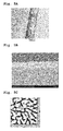
- a cross-section of a concavity and convexity structure of the block copolymer has a smooth chevron shape. Accordingly, the concavity and convexity structure of the block copolymer can be completely covered with a seed layer having a uniform film thickness and it is possible to manufacture an electroformed mold having high mechanical strength without causing a pattern defect or the like.
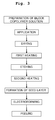
- the method for producing the mold mainly includes a step (processing) of preparing a block copolymer solution, a step for applying the block copolymer solution, a drying step, a first heating step, an etching step, a second heating step, a seed layer forming step, an electroforming step, and a releasing or peeling step.
- a step (processing) of preparing a block copolymer solution a step for applying the block copolymer solution
- a drying step a first heating step, an etching step, a second heating step, a seed layer forming step, an electroforming step, and a releasing or peeling step.
- the block copolymer used for the present invention includes at least a first polymer segment made of a first homopolymer and a second polymer segment made of a second homopolymer different from the fist homopolymer.
- the second homopolymer desirably has a solubility parameter which is higher than a solubility parameter of the first homopolymer by 0.1 to 10 (cal/cm 3 ) 1/2 .
- the difference between the solubility parameters of the first and second homopolymers is less than 0.1 (cal/cm 3 ) 1/2 , it is difficult to form a regular micro phase separation structure of the block copolymer.
- the difference exceeds 10 (cal/cm 3 ) 1/2 , it is difficult to prepare a uniform solution of the block copolymer.
- Examples of monomers serving as raw materials of homopolymers usable as the first homopolymer and second homopolymer include styrene, methylstyrene, propylstyrene, butylstyrene, hexylstyrene, octylstyrene, methoxystyrene, ethylene, propylene, butene, hexene, acrylonitrile, acrylamide, methyl methacrylate, ethyl methacrylate, propyl methacrylate, butyl methacrylate, hexyl methacrylate, octyl methacrylate, methyl acrylate, ethyl acrylate, propyl acrylate, butyl acrylate, hexyl acrylate, octyl acrylate, methacrylic acid, acrylic acid, hydroxyethyl methacrylate, hydroxyethyl acrylate,
- styrene methyl methacrylate, ethylene oxide, butadiene, isoprene, vinylpyridine, and lactic acid are preferably used from the viewpoints that the formation of phase separation easily occurs, and that the concavities and convexities are easily formed by an etching.
- examples of a combination of the first homopolymer and the second homopolymer include combinations of two selected from the group consisting of a styrene-based polymer (more preferably polystyrene), polyalkyl methacrylate (more preferably polymethyl methacrylate), polyethylene oxide, polybutadiene, polyisoprene, polyvinylpyridine, and polylactic acid.
- a styrene-based polymer more preferably polystyrene
- polyalkyl methacrylate more preferably polymethyl methacrylate
- polyethylene oxide polybutadiene
- polyisoprene polyvinylpyridine
- polylactic acid examples of a combination of the first homopolymer and the second homopolymer
- a combination of the styrene-based polymer and polyalkyl methacrylate, a combination of the styrene-based polymer and polyethylene oxide, a combination of the styrene-based polymer and polyisoprene, a combination of the styrene-based polymer and polybutadiene are more preferable, and the combination of the styrene-based polymer and polymethyl methacrylate, the combination of the styrene-based polymer and polyisoprene, the combination of the styrene-based polymer and polybutadiene are particularly preferable, from the viewpoint that the depths of the concavities and convexities formed in the block copolymer can be further increased by preferentially removing one of the homopolymers by the etching process.
- a combination of polystyrene (PS) and polymethyl methacrylate (PMMA) is further preferable.
- the number average molecular weight (Mn) of the block copolymer is preferably 500,000 or more, and is more preferably 1,000,000 or more, and particularly preferably 1,000,000 to 5,000,000. In a case that the number average molecular weight is less than 500,000, the average pitch of the concavities and convexities formed by the micro phase separation structure of the block copolymer is so small that the average pitch of the concavities and convexities of the obtained diffraction grating becomes insufficient.
- the average pitch is desirably 100 to 600 nm, and thus the number average molecular weight (Mn) of the block copolymer is preferably 500,000 or more.
- Mn number average molecular weight of the block copolymer
- the molecular weight distribution (Mw/Mn) of the block copolymer is preferably 1.5 or less, and is more preferably 1.0 to 1.35. In a case that the molecular weight distribution exceeds 1.5, it is difficult to form the regular micro phase separation structure of the block copolymer.
- the number average molecular weight (Mn) and the weight average molecular weight (Mw) of the block copolymer are values measured by gel permeation chromatography (GPC) and converted to molecular weights of standard polystyrene.
- a volume ratio between the first polymer segment and the second polymer segment is desirably 3:7 to 7:3 in order to create a lamellar structure by self-organization or assembly, and is more preferably 4:6 to 6:4.
- the volume ratio is out of the above-described range, a concavity and convexity pattern owing to the lamellar structure is difficult to form.
- the block copolymer solution used in the present invention is prepared by dissolving the block copolymer in a solvent.
- the solvent include aliphatic hydrocarbons such as hexane, heptane, octane, decane, and cyclohexane; aromatic hydrocarbons such as benzene, toluene, xylene, and mesitylene; ethers such as diethyl ether, tetrahydrofuran, and dioxane; ketones such as acetone, methyl ethyl ketone, isophorone, and cyclohexanone; ether alcohols such as butoxyethyl ether, hexyloxyethyl alcohol, methoxy-2-propanol, and benzyloxyethanol; glycol ethers such as ethylene glycol dimethyl ether, diethylene glycol dimethyl ether, triglyme, propylene glycol monomethyl ether, and propylene
- the block copolymer solution may further include a different homopolymer (a homopolymer other than the first homopolymer and the second homopolymer in the block copolymer contained in the solution: for example, when the combination of the first homopolymer and the second homopolymer in the block copolymer is the combination of polystyrene and polymethyl methacrylate, the different homopolymer may be any kind of homopolymer other than polystyrene and polymethyl methacrylate), a surfactant, an ionic compound, an anti-foaming agent, a leveling agent, and the like.
- a different homopolymer a homopolymer other than the first homopolymer and the second homopolymer in the block copolymer contained in the solution: for example, when the combination of the first homopolymer and the second homopolymer in the block copolymer is the combination of polystyrene and polymethyl methacrylate, the different homopolymer may be any kind
- the micro phase separation structure of the block copolymer can be improved.
- polyalkylene oxide can be used to increase the depths of the concavities and convexities formed by the micro phase separation structure.
- polyalkylene oxide polyethylene oxide or polypropylene oxide is more preferable, and polyethylene oxide is particularly preferable.
- polyethylene oxide one represented by the following formula is preferable: HO-(CH 2 -CH 2 -O) n -H [in the formula, n represents an integer of 10 to 5000 (more preferably an integer of 50 to 1000, and further preferably an integer of 50 to 500)].
- n is less than the lower limit
- the molecular weight is so low that the effect obtained by containing the different homopolymer becomes insufficient, because the polyethylene oxide is lost due to volatilization, vaporization, or the like during a heating process at a high-temperature.
- the value exceeds the upper limit the molecular weight is so high that the molecular mobility is low. Hence, the speed of the phase separation is lowered, and the formation of the micro phase separation structure is adversely affected.
- the number average molecular weight (Mn) of the different homopolymer is preferably 460 to 220,000, and is more preferably 2,200 to 46,000.
- the number average molecular weight is less than the lower limit, the molecular weight is so low that the effect obtained by containing the different homopolymer becomes insufficient, because the different homopolymer is lost due to volatilization, vaporization, or the like during the heating process at the high-temperature.
- the number average molecular weight exceeds the upper limit, the molecular weight is so high that the molecular mobility is low. Hence, the speed of the phase separation is lowered, and the formation of the micro phase separation structure is adversely affected.
- the molecular weight distribution (Mw/Mn) of the different homopolymer is preferably 1.5 or less, and more preferably 1.0 to 1.3. In a case that the molecular weight distribution exceeds the upper limit, uniformity of the shape of the micro phase separation is less likely to be maintained.
- Mn and Mw are values measured by gel permeation chromatography (GPC) and converted to molecular weights of standard polystyrene.
- the combination of the first homopolymer and the second homopolymer in the block copolymer be the combination of polystyrene and polymethyl methacrylate (polystyrene-polymethyl methacrylate), and that the different homopolymer be a polyalkylene oxide.
- the content thereof is preferably 100 parts by mass or less, and more preferably 5 parts by mass to 100 parts by mass, relative to 100 parts by mass of the block copolymer. In a case that the content of the different homopolymer is less than the lower limit, the effect obtained by containing the different homopolymer becomes insufficient.
- the content thereof is preferably 10 parts by mass or less relative to 100 parts by mass of the block copolymer.
- the content thereof is preferably 10 parts by mass or less relative to 100 parts by mass of the block copolymer.
- the total percentage content of the block copolymer and the different homopolymer is preferably 0.1 to 15% by mass, and more preferably 0.3 to 5% by mass, in the block copolymer solution.
- the total percentage content is less than the lower limit, it is difficult to uniformly apply the solution to attain a film thickness sufficient to obtain a necessary film thickness.
- the total percentage content exceeds the upper limit, it is relatively difficult to prepare a solution in which the block copolymer and the different homopolymer are uniformly dissolved in the solvent.
- the block copolymer solution prepared as described above is applied on a base member 10 to form a thin film 30.
- the base member 10 is not especially limited, and is exemplified, for example, by substrates of resins such as polyimide, polyphenylene sulfide (PPS), polyphenylene oxide, polyether ketone, polyethylene naphthalate, polyethylene terephthalate, polyarylate, triacetyl cellulose, and polycycloolefin; inorganic substrates such as glass, octadecyldimethyl chlorosilane (ODS) treated glass, octadecyl trichlorosilane (OTS) treated glass, organo silicate treated glass, and silicon substrates; and substrates of metals such as aluminum, iron, and copper.
- resins such as polyimide, polyphenylene sulfide (PPS), polyphenylene oxide, polyether ketone, polyethylene naphthalate, polyethylene ter
- the base member 10 may be subjected to surface treatments such as an orientation treatment.
- surface treatments such as an orientation treatment.
- the micro phase separation structure such as the lamellar structure, a cylinder structure, and a globular or spherical structure is more likely to be arranged perpendicular to the surface in a heating step as will be described later on.
- the reason thereof is that domain of each block forming the block copolymer is more likely to be perpendicularly-oriented by decreasing the difference in interface energy between each block copolymer component and the surface of the substrate.
- the method for applying the block copolymer solution is not particularly limited, and, for example, a spin coating method, a spray coating method, a dip coating method, a dropping method, a gravure printing method, a screen printing method, a relief printing method, a die coating method, a curtain coating method, or an ink-jet method can be employed as the method.
- the thickness of the thin film 30 of the block copolymer is preferably within a range which allows the thickness of a dried coating film, as will be described later, to be 10 to 3000 nm, and more preferably within a range which allows the thickness of the dried coating film to be 50 to 500 nm.
- the thin film 30 on the base member 10 is dried.
- the drying can be performed in the ambient atmosphere.
- the temperature for drying the thin film 30 is not particularly limited, provided that the solvent can be removed from the thin film 30.
- the temperature is preferably 30 degrees Celsius to 200 degrees Celsius, and more preferably 40 degrees Celsius to 100 degrees Celsius. It is noted that concavities and convexities are found, in some cases, on the surface of the thin film 30 when the formation of the micro phase separation structure of the block copolymer is started during the drying step.
- the thin film 30 is heated at a temperature of not less than a glass transition temperature (Tg) of the block copolymer (first heating step or annealing process).
- the heating step promotes the self-organization or assembly of the block copolymer, and the micro phase separation of the block copolymer into portions of a first polymer segment 32 and second polymer segment 34 occurs as shown in Fig. 1(B) .
- the heating temperature is less than the glass transition temperature of the block copolymer, the molecular mobility of the polymer is so low that the self-organization or assembly of the block copolymer does not make progress adequately and thus the micro phase separation structure can not be formed enough or the heating time required for sufficiently generating the micro phase separation structure is long.
- the upper limit of the heating temperature is not particularly limited, unless the block copolymer is pyrolyzed at the temperature.
- the first heating step can be performed in the ambient atmosphere using an oven or the like.
- the drying step and the heating step can be performed continuously by gradually increasing the heating temperature. Accordingly, the drying step is included in the heating step.
- the etching process of the thin film 30 is performed. Since the molecular structure of the first polymer segment 32 is different from the molecular structure of the second polymer segment 34, etchability of the first polymer segment 32 is also different from that of the second polymer segment 34. Therefore, by performing the etching process depending on each type of the polymer segments, that is, depending on each type of homopolymer, it is possible to selectively remove one of the polymer segments (second polymer segment 34) forming the block copolymer. A remarkable concavity and convexity structure appears on the coating film by removing each second polymer segment 34 from the micro phase separation structure in the etching process, as shown in Fig. 1(C) schematically.
- an etching method using, for example, a reactive ion etching method, an ozone oxidation method, a hydrolysis method, a metal ion staining method, an ultraviolet-ray etching method, or the like can be employed.
- a method may be employed in which covalent bonds in the block copolymer are cleaved by treating the covalent bonds with at least one selected from the group consisting of acids, bases, and reducing agents, and then the coating film in which the micro phase separation structure is formed is cleaned with a solvent which dissolves only one of the polymer segments, or the like, thereby removing only the one of the polymer segments, while keeping the micro phase separation structure.
- the ultraviolet-ray etching is used in view of operability and the like.
- the second heating process or the annealing process is performed to a concavity and convexity structure 36 of the thin film 30 obtained by the etching step.
- the heating temperature in the second heating process is desirably not less than the glass transition temperature of the first polymer segment 32 remaining after the etching, that is, not less than the glass transition temperature of the first homopolymer.
- the heating temperature in the second heating process is desirably not less than the glass transition temperature of the first homopolymer and not more than a temperature higher than the glass transition temperature of the first homopolymer by 70 degrees Celsius.
- the heating temperature is less than the glass transition temperature of the first homopolymer, it is not possible to obtain a desired concavity and convexity structure (that is, a smooth chevron structure) after the electroforming, or a long time is required to perform the heating.
- the heating temperature is much higher than the glass transition temperature of the first homopolymer, the first polymer segment 32 is melted and/or the shape of the first polymer segment 32 is collapsed severely. Thus, it is not preferable.
- the heating is desirably performed within a range from the glass transition temperature to the temperature higher than the glass transition temperature by about 70 degrees Celsius. Similar to the first heating process, the second heating process can be performed in the ambient atmosphere using the oven or the like.
- a distribution of the pitch is required to be such that diffraction occurs in a wavelength region such as the visible region including a wavelength range which is wide and includes relatively long wavelength.
- a block copolymer having a relatively high molecular weight it is necessary to reliably obtain, by the electroforming, a concavity and convexity structure having the desired pitch distribution.
- a metallic mold in which the concavity and convexity structure is also reflected enough, is successfully obtained in the subsequent electroforming step.
- the concavity and convexity structure 36 after the etching is considered to have a complicated cross-section structure, in which the side surfaces of grooves defined by the concavity and convexity structure are coarse and the concavities and convexities (including the overhang) are generated in a direction perpendicular to a thickness direction.
- the following three problems are arisen by the complicated cross-section structure.
- each cross-section shape defined by the first polymer segment 32 is formed of a relatively smooth and sloped surface to have a shape of chevron narrowing upward from the base member (referred to as "chevron-shaped structure" in this invention).
- the overhang does not appear in such chevron-shaped structure, and the chevron-shaped structure is duplicated into the inverted pattern in a metal layer accumulated on the first polymer segment 32, thereby the metal layer can be released easily.
- Fig. 5B is a micrograph, taken by a scanning electron microscope (SEM), showing the cross-section structure of the mold, which is formed, by Ni-electroforming using the concavity and convexity structure obtained by the heating process after the etching process of the block copolymer, in Example 1 which will be described later.
- SEM scanning electron microscope
- FIG. 14A is a SEM micrograph showing the cross-section structure of the mold, which is formed by the Ni-electroforming (nickel electroforming) using the concavity and convexity structure obtained without the second heating process after the etching process of the block copolymer, in Comparative Example 1 which will be described later. It has been appreciated that Ni portions corresponding to white portions in Fig. 14A form grooves each having a complicated shape including an overhang structure; and that the resins (black portions in Fig. 14A ) are penetrated or entered into the grooves.
- Ni-electroforming nickel electroforming
- the average pitch of the concavities and convexities representing the chevron-shaped structure 38 is preferably within a range from 100 to 600 nm, and more preferably 200 to 600 nm. In a case that the average pitch of the concavities and convexities is less than the lower limit, the pitches are so small relative to wavelengths of the visible light that required diffraction of the visible light is less likely to occur by using the diffraction grating obtained by use of such a master.
- the average pitch of the concavities and convexities refers to an average value of pitches of the concavities and convexities obtained when pitches of the concavities and convexities on the surface of the cured resin layer (distances between adjacent concave portions or between adjacent convex portions) are measured.
- a value which can be calculated as follows is employed as such average value of the pitches of the concavities and convexities.
- a concavity and convexity analysis image is obtained by measuring the shape of the concavities and convexities on the surface by use of a scanning probe microscope (for example, one manufactured by SII Nano Technology Inc., under the product name of "E-sweep", or the like), then the distances between randomly selected adjacent convex portions or the distances between randomly selected adjacent concave portions are measured at 100 points or more in the concavity and convexity analysis image, and then an average of these distances is determined as the average value of the pitches of concavities and convexities.
- a scanning probe microscope for example, one manufactured by SII Nano Technology Inc., under the product name of "E-sweep", or the like
- the average height of the concavities and convexities representing the chevron-shaped structure 38 is preferably within a range from 5 to 200 nm, more preferably within a range from 20 to 200 nm, and further preferably within a range from 50 to 150 nm.
- the average height of the concavities and convexities is less than the lower limit, the height is so small relative to the wavelengths of the visible light that the diffraction is insufficient.
- the average height exceeds the upper limit, the following tendency is found.
- the element When the obtained diffraction grating is used as an optical element on the light extraction port side of the organic EL element, the element tends to be easily destructed and the life thereof tends to be shortened because of heat generation which occurs when the electric field distribution in the EL layer becomes non-uniform, and hence electric fields concentrate on a certain position or area.
- the average height of the concavities and convexities refers to an average value of the heights of the concavities and convexities obtained when heights of the concavities and convexities (the distances between concave portions and convex portions in the depth direction) on the surface of the cured resin layer are measured.
- a value calculated as follows is employed as the average value of the heights of the concavities and convexities. That is, a concavity and convexity analysis image is obtained by measuring the shape of the concavities and convexities on the surface by use of the scanning probe microscope (for example, one manufactured by SII NanoTechnology Inc., under the product name of "E-sweep", or the like), then the distances between randomly selected concave portions and convex portions in the depth direction are measured at 100 points or more in the concavity and convexity analysis image, and then the average of the distances is determined as the average value of heights of concavities and convexities.
- the scanning probe microscope for example, one manufactured by SII NanoTechnology Inc., under the product name of "E-sweep", or the like
- a seed layer 40 functioning as an electroconductive layer for a subsequent electroforming process is formed on the surface of the chevron-shaped structure 38 of the master obtained as described above.
- the seed layer 40 can be formed by non-electrolytic plating, sputtering, or vapor deposition.
- the thickness of the seed layer 40 is preferably not less than 10 nm and more preferably not less than 100 nm to uniformalize current density during the subsequent electroforming process, and thereby making the thickness of the metal layer accumulated by the subsequent electroforming process to be constant.
- the seed layer As a material of the seed layer, it is possible to use, for example, nickel, copper, gold, silver, platinum, titanium, cobalt, tin, zinc, chrome, gold-cobalt alloy, gold-nickel alloy, boron-nickel alloy, solder, copper-nickel-chromium alloy, tin-nickel alloy, nickel-palladium alloy, nickel-cobalt-phosphorus alloy, or alloy thereof. It is considered that the relatively smooth chevron-shaped structure as shown in Fig. 1(D) is more likely to be attached to by the seed layer completely and with a uniform thickness, compared with the complicated cross-section structure as shown in Fig, 1(C) .
- the entire thickness of a metal layer 50 including the thickness of the seed layer 40 can be, for example, 10 to 3000 ⁇ m.
- a material of the metal layer 50 accumulated by the electroforming it is possible to use any of metal species as described above which can be used as the seed layer 40.
- nickel is preferable. In this case, nickel is also preferably used for the seed layer 40.
- the current density during the electroforming may be, for example, 0.03 to 10 A/cm 2 for suppressing bridge to form a uniform metal layer and in view of shortening of an electroforming time.
- the formed metal layer 50 desirably has appropriate hardness and thickness.
- a diamond like carbon (DLC) process or a Cr plating processing treatment can be performed on the surface of the metal layer in order to improve the hardness of the metal layer formed by the electroforming.
- the hardness of the surface may be improved by further performing the heating process of the metal layer.
- the metal layer 50 including the seed layer obtained as described above is peeled off from the base member having the concavity and convexity structure to obtain a mold as a father die.
- the metal layer 50 may be peeled off physically, or the first homopolymer and the remained block copolymer may be dissolved to be removed by using an organic solvent dissolving them, such as toluene, tetrahydrofuran (THF), and chloroform.
- each part 60 remained in the mold can be removed by a cleaning.
- a cleaning method a wet cleaning or a dry cleaning can be used.
- the wet cleaning the remained parts can be removed by performing the cleaning with the organic solvent such as toluene and tetrahydrofuran, the surfactant, or an alkaline solution.
- an ultrasonic cleaning may be carried out.
- the remained parts may be removed by performing an electrolytic cleaning.
- the dry cleaning the remained parts can be removed by an ashing using ultraviolet rays and/or plasma.
- the wet cleaning and the dry cleaning may be used in combination.
- a rinse process with pure water or purified water may be performed, and then ozone irradiation may be carried out after a drying. Accordingly, a mold 70 having a desired concavity and convexity structure is obtained.
- a mold-release treatment of the mold 70 may be performed to improve the mold releasability from the resin.
- the mold-release treatment a manner to decrease surface energy is commonly used, and the mold-release treatment is not particularly limited and includes, for example, a method in which a concave and convex surface 70a of the mold 70 is coated with a mold-release agent such as a fluorine-based material and a silicon resin as shown in Fig. 2(A) , a method in which the surface is subjected to a treatment using a fluorine-based silane coupling agent, and a method in which a film of a diamond like carbon is formed on the surface.
- a mother die is produced by transferring the concavity and convexity structure (pattern) of the mold to a layer formed of an organic material such as resin or an inorganic material such as a sol-gel material.
- a resin layer 80 as a layer to which the concavity and convexity pattern is transferred, as an example.
- the curable resin is applied on a transparent supporting substrate 90, and then the resin layer 80 is cured while pressing the concavity and convexity structure of the mold 70 against the resin layer 80, as shown in Fig. 2(B) .
- the transparent supporting substrate 90 is exemplified, for example, by base members made of a transparent inorganic substance such as glass; base members made of a resin such as polyethylene terephthalate (PET), polyethylene diaphthalate (PEN), polycarbonate (PC), cycloolefin polymer (COP), polymethyl methacrylate (PMMA), or polystyrene (PS); stacked base members having a gas barrier layer made of an inorganic substance such as SiN, SiO 2 , SiC, SiO 2 N y , TiO 2 , or Al 2 O 3 formed on the surface of the base member made of any of the above-described resins; and stacked base members having base members made of any of the above-described resins and gas barrier layers made of any of the above-described inorganic substances stacked alternately on each other.
- the thickness of the transparent supporting substrate may be within a range from 1 to 500 ⁇ m.
- the curable resin examples include epoxy resin, acrylic resin, urethane resin, melamine resin, urea resin, polyester resin, phenol resin, and cross-linking type liquid crystal resin.
- the thickness of the cured resin is preferably within a range from 0.5 to 500 ⁇ m. In a case that the thickness is less than the lower limit, heights of the concavities and convexities formed on the surface of the cured resin layer are more likely to be insufficient. In a case that the thickness exceeds the upper limit, an effect of volume change of the resin which occurs during upon curing is likely to be so large that the formation of the shape of the concavities and convexities tends to be insufficient.
- the condition for curing the curable resin varies depending on the kind of the resin used.
- a curing temperature is preferably within a range from room temperature to 250 degrees Celsius
- a curing time is preferably within a range from 0.5 minutes to 3 hours.
- the curable resin is cured by irradiation with energy rays such as ultraviolet rays or electron beams.
- energy rays such as ultraviolet rays or electron beams.
- the amount of the irradiation is preferably within a range from 20 mJ/cm 2 to 5 J/cm 2 .
- the mold 70 is detached from the cured rein layer 80 in a cured state.
- a method for detaching the mold 70 is not limited to a mechanical peeling method, and can adopt any known method.
- the resin film structure 100 may be used, as it is, as the diffraction grating.
- the resin film structure 100 is further used as the mold to make a diffraction grating made of the organic material such as the resin or a structure made of the inorganic material such as the sol-gel material, and the structure made of the organic material or the structure made of the inorganic material can be used as the diffraction grating.
- the method for producing the mold of the present invention can be used not only in production of the diffraction grating provided on the light extraction port side of the organic EL element but also in production of an optical component having a minute or fine pattern used for various devices.
- the method for producing the mold of the present invention can be used to produce a wire grid polarizer, an antireflection film, or an optical element for providing a light confinement effect in a solar cell by being placed on the photoelectric conversion surface side of the solar cell.
- the resin film structure 100 having a desired pattern can be obtained.
- the resin film structure 100 obtained through the transfer process of the mold as described above is used as the mother die; a curable resin layer 82 is applied on another transparent supporting substrate 92 as shown in Fig. 2(D) ; and the curable resin layer 82 is cured while pressing the resin film structure 100 against the curable resin layer 82, similar to a case in which the resin film structure 100 is formed. Subsequently, the resin film structure 100 is peeled off from the curable resin layer 82 in a cured state. Accordingly, a replica 110 as another resin film structure as shown in Fig.
- 2(E) can be obtained. Further, it is allowable to produce a replica having the inverted pattern of the replica 110 by performing the above transfer step using the replica 110 as a master and/or to produce a sub-replica by repeating the above transfer step again using the replica having the inverted pattern as the master.
- a method for forming a substrate having a concavity and convexity pattern using the sol-gel material mainly includes: a solution preparation step for preparing a sol solution; an application step for applying the prepared sol solution on the substrate; a drying step for drying the coating film of the sol solution applied on the substrate; a pressing step for pressing a mold with a transfer pattern; a pre-sintering step during which the coating film to which the mold is pressed is subjected to the pre-sintering; a peeling step for peeling off the mold from the coating film; and a main sintering step during which the coating film is subjected to the main sintering.
- a solution preparation step for preparing a sol solution an application step for applying the prepared sol solution on the substrate
- a drying step for drying the coating film of the sol solution applied on the substrate a pressing step for pressing a mold with a transfer pattern
- a pre-sintering step during which the coating film to which the mold is pressed is subjected to the pre-s
- a sol-gel solution is prepared to form a coating film to which a pattern is transferred by a sol-gel method.
- a sol-gel method For example, in a case that silica is synthesized by the sol-gel method on the substrate, the sol solution of metal alkoxide (silica precursor) is prepared.
- the silica precursor is exemplified by metal alkoxides including, for example, tetraalkoxide monomers such as tetramethoxysilane (TMOS), tetraethoxysilane (TEOS), tetra-i-propoxysilane, tetra-n-propoxysilane, tetra-i-butoxysilane, tetra-n-butoxysilane, tetra-sec-butoxysilane, and tetra-t-butoxysilane; trialkoxide monomers such as methyl trimethoxysilane, ethyl trimethoxysilane, propyl trimethoxysilane, isopropyl trimethoxysilane, phenyl trimethoxysilane, methyl triethoxysilane, ethyl triethoxysilane, propyl triethoxysilane, isopropyl triethoxysi
- the silica precursor is exemplified, for example, by metal acetylacetonate, metal carboxylate, oxychloride, chloride, and mixtures thereof.
- the silica precursor is not limited thereto.
- metal species include, in addition to Si, Ti, Sn, Al, Zn, Zr, In, and mixtures thereof, but are not limited thereto. It is also possible to use any appropriate mixture of precursors of the above oxidized metals.
- the mixture ratio thereof can be 1:1, for example, in a molar ratio.
- the sol solution produces amorphous silica by performing hydrolysis and polycondensation reaction.
- An acid such as hydrochloric acid or an alkali such as ammonia is added in order to adjust pH of the solution as a synthesis condition.
- the pH is preferably not more than 4 or not less than 10.
- Water may be added to perform the hydrolysis. An amount of water to be added can be 1.5 times or more with respect to metal alkoxide species in the molar ratio.
- the solvent examples include alcohols such as methanol, ethanol, isopropyl alcohol (IPA), and butanol; aliphatic hydrocarbons such as hexane, heptane, octane, decane, and cyclohexane; aromatic hydrocarbons such as benzene, toluene, xylene, and mesitylene; ethers such as diethyl ether, tetrahydrofuran, and dioxane; ketones such as acetone, methyl ethyl ketone, isophorone, and cyclohexanone; ether alcohols such as butoxyethyl ether, hexyloxyethyl alcohol, methoxy-2-propanol, and benzyloxyethanol; glycols such as ethylene glycol and propylene glycol; glycol ethers such as ethylene glycol dimethyl ether, diethylene glycol dimethyl ether, and propylene glycol monomethyl
- polyethylene glycol polyethylene oxide, hydroxypropylcellulose, and polyvinyl alcohol for viscosity adjustment
- alkanolamine such as triethanolamine as a solution stabilizer
- ⁇ -diketone such as acetylacetone
- ⁇ -ketoester formamid
- dimetylformamide dioxane
- the sol solution prepared as described above is applied on the substrate.
- substrates made of inorganic materials such as glass, silica glass, and silicon substrates or substrates of resins such as polyethylene terephthalate (PET), polyethylene diaphthalate (PEN), polycarbonate (PC), cycloolefin polymer (COP), polymethyl methacrylate (PMMA), polystyrene (PS), polyimide (PI), and polyarylate may be used.
- the substrate may be transparent or opaque. In a case that a substrate having a concavity and convexity pattern obtained from the substrate is used for production of the organic EL element as will be described later, the substrate desirably has resistance to heat and ultraviolet (UV) light etc.
- UV ultraviolet
- the substrates made of the inorganic materials such as the glass, the silica glass, and the silicon substrates are more preferable. It is allowable to perform a surface treatment or provide an easy-adhesion layer on the substrate in order to improve adhesion property and to provide a gas barrier layer in order to keep out moisture and/or gas such as oxygen.
- a method for applying the sol solution it is possible to use any application method such as a bar coating method, a spin coating method, a spray coating method, a dip coating method, a die coating method, and an ink-jet method.
- the bar coating method, the die coating method, and the spin coating method are preferable, because the sol solution can be uniformly applied on the substrate having a relatively large area and the application can be quickly completed prior to gelation of the sol solution. It is noted that, since a desired concavity and convexity pattern by a sol-gel material layer is formed in subsequent steps, the surface of the substrate (including the surface treatment or the easy-adhesion layer in case that the surface treatment or the easy-adhesion layer is present) may be flat, and the substrate itself does not have the desired concavity and convexity pattern.
- the substrate is kept in the atmosphere or under reduced pressure to evaporate the solution in the applied coating film (hereinafter referred to also as "sol-gel material layer" as appropriate).
- the resin film structure 100 (mold) is pressed against the coating film. In this situation, the resin film structure 100 may be pressed by using a pressing roll.
- a period of time during which the mold and the coating film are brought in contact with each other in a roll process is shorter than that in a pressing system, and thus there are advantages such that it is possible to prevent deformation of pattern due to difference among coefficients of thermal expansion of the mold, the substrate, a stage on which the substrate is provided, and the like; it is possible to prevent generation of bubbles of gas in the pattern due to bumping of the solvent in the gel solution or to prevent trace or mark of gas from being left; it is possible to reduce transfer pressure and peeling force due to line contact with the substrate (coating film), and thereby making it possible to deal with a larger substrate readily; no bubble is included during the pressing; and the like. Further, the heating may be performed while pressing the resin film structure 100.
- the coating film may be subjected to the pre-sintering.
- the pre-sintering promotes gelation of the coating film to solidify the pattern, and thereby the pattern is less likely to be collapsed during the peeling.
- the heating is preferably performed at a temperature from 40 degrees Celsius to 150 degrees Celsius in the atmosphere. It is not indispensable to perform the pre-sintering.
- the resin film structure 100 is peeled off from the coating film (sol-gel material layer) after the pressing step or the pre-sintering step.
- the peeling force may be smaller than that in a case that a plate-shaped mold is used, and it is possible to easily peel off the mold from the coating film without remaining the coating film in the mold.
- the coating film is subjected to the main sintering. Hydroxyl group and the like contained in silica (amorphous silica) forming the coating film is desorbed or eliminated by the main sintering to further strengthen the coating film.
- the main sintering may be performed at a temperature from 200 degrees Celsius to 1200 degrees Celsius for about 5 minutes to 6 hours.
- the coating film is cured, and thereby obtaining a sol-gel structure (diffraction grating) with a concavity and convexity pattern film which corresponds to the concavity and convexity pattern of the resin film structure 100, that is, a sol-gel structure (diffraction grating) in which the sol-gel material layer having the concavity and convexity pattern is directly formed on the flat substrate.
- a sol-gel structure diffiffraction grating in which the sol-gel material layer having the concavity and convexity pattern is directly formed on the flat substrate.
- the silica as the sol-gel material layer is amorphous, crystalline, or in a mixture state of the amorphous and the crystalline.
- a film may be laminated or stacked, on the surface of the resin film structure 100 or the replica 110 (or sol-gel structure) having the concavity and convexity pattern, by a gas phase method such as an evaporation method or a sputtering method.
- a gas phase method such as an evaporation method or a sputtering method.
- the vapor-deposited film examples include metals such as aluminum, gold, silver, platinum, and nickel; and metal oxides such as aluminum oxide.
- the thickness of the vapor-deposited film is preferably 5 to 500 nm. In a case that the thickness is less than the lower limit, a uniform film is difficult to obtain, so that sufficient effect of lowering the adhesion is decreased. In a case that the thickness exceeds the upper limit, the shape of the master block is more likely to be dull.
- postcure may be conducted as appropriate by, for example, ultraviolet light irradiation, after curing of the resin.
- the curable resins 80, 82 are applied on the transparent supporting substrates 90, 92, respectively.
- the curable resin is applied directly on the surface of the mold 70 which is the master block or the surface of the cured resin layer 80, and then the cured resin is detached.
- a transparent electrode denoted by a reference numeral 3 is stacked on a resin layer 80 of the resin film 100 to maintain a concavity and convexity structure formed on the surface of the resin 80.
- a material for the transparent electrode 3 for example, indium oxide, zinc oxide, tin oxide, indium-tin oxide (ITO), which is a composite material thereof, gold, platinum, silver, or copper is used. Of these materials, ITO is preferable from the viewpoint of the transparency and the electrical conductivity.
- the thickness of the transparent electrode 3 is preferably within a range from 20 to 500 nm. In a case that the thickness is less than the lower limit, the electrical conductivity is more likely to be insufficient.
- any known method such as a vapor deposition method or a sputtering method can be employed as appropriate.
- the vapor deposition method is preferably employed from the viewpoint of maintaining the shape of the concavities and convexities formed on the surface of the cured resin layer; and the sputtering method is preferably employed from the viewpoint of improving adhesion property. It is allowable to put a glass substrate on a side opposite to the resin layer 80 of the resin film 100 before the transparent electrode 3 is provided on the resin layer 80.
- an organic layer denoted by a reference numeral 4 as shown in Fig. 4 is stacked on the transparent electrode 3 to maintain the shape of the concavities and convexities formed on the surface of the resin 80.
- the organic layer 4 is not particularly limited, provided that the organic layer 4 is one usable as an organic layer of the organic EL element.
- any known organic layer can be used as appropriate.
- the organic layer 4 may be a stacked body of various organic thin films, and, for example, may be a stacked body of an anode buffer layer 11, a hole transporting layer 12, and an electron transporting layer 13 as shown in Fig. 4 .
- examples of materials for the anode buffer layer 11 include copper phthalocyanine, PEDOT, and the like.
- Examples of materials for the hole transporting layer 12 include derivatives of triphenylamine, triphenyldiamine derivatives (TPD), benzidine, pyrazoline, styrylamine, hydrazone, triphenylmethane, carbazole, and the like.
- Examples of materials for the electron transporting layer 13 include aluminum-quinolinol complex (Alq), phenanthroline derivatives, oxadiazole derivatives, triazole derivatives, phenylquinoxaline derivatives, silole derivatives, and the like.
- the organic layer 4 may be, for example, a stacked body of a hole injecting layer made of a triphenylamine derivative or the like, and a light emitting layer made of a fluorescent organic solid such as anthracene, a stacked body of the light emitting layer and an electron injecting layer made of a perylene derivative or the like, or a stacked body of these hole injecting layer, light emitting layer, and electron injecting layer.
- the organic layer 4 may be a stacked body of the hole transporting layer, the light emitting layer, and the electron transporting layer as exemplified in Example 22 as will be described later on.
- examples of materials of the hole transporting layer include aromatic diamine compounds such as phthalocyanine derivatives, naphthalocyanine derivatives, porphyrin derivatives, N,N'-bis(3-methylphenyl)-(1,1'-biphenyl)-4,4'-diamine (TPD), and 4,4'-bis[N-(naphthyl)-N-phenyl-amino]biphenyl( ⁇ -NPD); oxazole; oxadiazole; triazole; imidazole; imidazolone; stilbene derivatives; pyrazoline derivatives; tetrahydroimidazole; polyarylalkane; butadiene; and 4,4',4"-tris(N-(3-methylphenyl)N-phen
- the materials of the hole transporting layer are not limited thereto.
- a hole injected from the transparent electrode and electron injected from a metal electrode are recombined to occur light emission.
- materials of the light emitting layer include metallo-organic complex such as anthracene, naphthalene, pyrene, tetracene, coronene, perylene, phthaloperylene, naphthaloperylene, diphenylbutadiene, tetraphenylbutadiene, coumarin, oxadiazole, bisbenzoxazoline, bisstyryl, cyclopentadiene, and aluminum-quinolinol complex (Alq3); tri-(p-terphenyl-4-yl)amine; 1-aryl-2,5-di(2-thienyl) pyrrole derivatives; pyran; quinacridone; rubren; distyrylbenzene derivatives; disty
- light-emitting materials selected from the above compounds are mixed as appropriate and then are used.
- a material system generating emission of light from a spin multiplet such as a phosphorescence emitting material generating emission of phosphorescence and a compound including, in a part of the molecules, a constituent portion formed by the above materials.
- the phosphorescence emitting material preferably includes heavy metal such as iridium.
- a host material having high carrier mobility may be doped with each of the light-emitting materials as a guest material to generate the light emission using dipole-dipole interaction (Forster mechanism), electron exchange interaction (Dexer mechanism).
- Examples of materials of the electron transporting layer include heterocyclic tetracarboxylic anhydrides such as nitro-substituted fluorene derivatives, diphenylquinone derivatives, thiopyran dioxide derivatives, and naphthaleneperylene; and metallo-organic complex such as carbodiimide, fluorenylidene methane derivatives, anthraquino dimethane and anthrone derivarives, oxadiazole derivatives, and aluminum-quinolinol complex (Alq3).
- heterocyclic tetracarboxylic anhydrides such as nitro-substituted fluorene derivatives, diphenylquinone derivatives, thiopyran dioxide derivatives, and naphthaleneperylene
- metallo-organic complex such as carbodiimide, fluorenylidene methane derivatives, anthraquino dimethane and anthrone derivarives,
- oxadiazole derivatives it is also possible to use, as an electron transporting material, thiadiazole derivatives in which oxygen atoms of oxadiazole rings are substituted by sulfur atoms and quinoxaline derivatives having quinoxaline rings known as electron attractive group.
- thiadiazole derivatives in which oxygen atoms of oxadiazole rings are substituted by sulfur atoms and quinoxaline derivatives having quinoxaline rings known as electron attractive group.
- a polymeric material in which the above materials are introduced into a macromolecular chain or the above materials are made to be a main chain of the macromolecular chain.
- the hole transporting layer or the electron transporting layer may also function as the light-emitting layer. In this case, there are two organic layers between the transparent electrode and the metal electrode which will be described later.
- a layer made of a metal fluoride such as lithium fluoride (LiF) or Li 2 O 3 , a highly active alkaline earth metal such as Ca, Ba, or Cs, an organic insulating material, or the like may be provided on the transparent electrode 3 or the organic layer 4.
- a layer made of triazole derivatives; oxadiazole derivatives; imidazole derivatives; polyarylalkane derivatives; pyrazoline derivatives and pyrazolone derivatives; phenylenediamine derivatives; arylamine derivatives; amino-substituted chalcone derivatives; oxazole derivatives; styrylanthracene derivatives; fluorenon derivatives; hydrazone derivatives; stilbene derivatives; silazane derivatives; aniline copolymer; or a conductive polymer oligomer, in particular, thiophene oligomer, may be provided between the organic layer and the transparent electrode as the hole injecting layer.
- the thicknesses of the anode buffer layer 11, the hole transporting layer 12, and the electron transporting layer 13 are preferably within a range from 1 to 50 nm, a range from 5 to 200 nm, and a range from 5 to 200 nm, respectively, from the viewpoint of maintaining the shape of the concavities and convexities formed on the surface of the cured resin layer.
- the thicknesses of the hole transporting layer, the light-emitting layer, and the electron transporting layer are preferably within a range from 1 to 200 nm, a range from 5 to 100 nm, and a range from 5 to 200 nm, respectively.
- any known method such as a vapor deposition method, a sputtering method, and a die coating method can be employed as appropriate.
- the vapor deposition method is preferably employed from the viewpoint of maintaining the shape of the concavities and convexities formed on the surface of the resin 80.
- a metal electrode denoted by a reference numeral 5 is stacked on the organic layer 4 so as to maintain the shape of the concavities and convexities formed on the surface of the resin 80 in the step for forming the organic EL element.
- Materials of the metal electrode 5 are not particularly limited, and a substance having a small work function can be used as appropriate. Examples of the materials include aluminum, MgAg, MgIn, and AlLi.
- the thickness of the metal electrode 5 is preferably within a range from 50 to 500 nm. In a case that the thickness is less than the lower limit, the electrical conductivity is more likely to be decreased.
- any known method such as a vapor deposition method and a sputtering method can be adopted to stack the metal electrode 5.
- the vapor deposition method is preferably employed from the viewpoint of maintaining the concavity and convexity structure formed on the surface of the resin 80. Accordingly, an organic EL element 200 having a structure as shown in Fig. 4 can be obtained.
- the resin 80 on the base member 10 has the chevron-shaped structure.
- each of the transparent electrode 3, the organic layer 4, and the metal electrode 5 is readily stacked to maintain the chevron-shaped structure of the resin 80.
- each of the transparent electrode 3, the organic layer 4, and the metal electrode 5 is more likely to have the same structure as the chevron-shaped structure formed on the surface of the resin layer 80, an inter-electrode distance between the transparent electrode 3 and the metal electrode 5 is partially short. For this reason, in comparison with those in which the inter-electrode distance between the transparent electrode 3 and the metal electrode 5 is uniform, an increase in electric field intensity can be expected in application of voltage, and also light emission efficiency of the organic EL element can be improved.
- the average height of the concavities and convexities formed on the surface (the cured surface of curable resin) of the diffraction grating is preferably within the range from 5 to 200 nm, more preferably within the range from 20 to 200 nm, and further preferably within the range from 50 to 150 nm as described above.
- the average pitch of the concavities and convexities formed on the surface (the cured surface of curable resin) of the diffraction grating is preferably within the range from 100 to 600 nm, and more preferably within the range from 200 to 600 nm as described above.
- an average value m and a median M of a depth distribution of the concavities and convexities on the cross-section obtained by a method which will be described later preferably satisfy the following expression: 1.062 m ⁇ 2.2533 ⁇ 0.95 ⁇ M ⁇ 1.062 m ⁇ 0.2533 ⁇ 1.05
- a kurtosis of the cross-section shape of the concavity and convexity structure formed on the surface (the surface of cured curable resin) of the diffraction grating is preferably -1.2 or more, and more preferably -1.2 to 1.2. In a case that the kurtosis is less than the lower limit, the leakage current is more likely to be generated when the diffraction grating is used for the organic EL element.
- the kurtosis exceeds the upper limit, the concavities and convexities on the surface (resin layer) of the diffraction grating are decreased. As a result, it is considered to cause the following situation. That is, not only the diffraction effect cannot be obtained sufficiently, but also the electric field is more likely to be concentrated on the portions of the projections, so that leakage currents are more likely to be generated.
- the kurtosis and a method for measuring the kurtosis will be described later on.
- polystyrene hereinafter referred to as "PS” in an abbreviated manner as appropriate
- PMMA polymethyl methacrylate
- the volume ratio of the first polymer segment and second polymer segment (the first polymer segment: the second polymer segment) in each block copolymer was calculated on the assumption that the density of polystyrene was 1.05 g/cm 3 , the density of polymethyl methacrylate was 1.19 g/ cm 3 .
- the number average molecular weights (Mn) and the weight average molecular weights (Mw) of polymer segments or polymers were measured by using gel permeation chromatography (Model No: "GPC-8020” manufactured by Tosoh Corporation, in which TSK-GEL SuperH1000, SuperH2000, SuperH3000, and SuperH4000 were connected in series).
- the glass transition temperatures (Tg) of polymer segments were measured by use of a differential scanning calorimeter (manufactured by Perkin-Elmer under the product name of "DSC7"), while the temperature was raised at a rate of temperature rise of 20 degrees Celsius/min over a temperature range from 0 to 200 degrees Celsius.
- the solubility parameters of polystyrene and polymethyl methacrylate were 9.0 and 9.3, respectively (see Kagaku Binran Ouyou Hen (Handbook of Chemistry, Applied Chemistry), 2nd edition).
- the obtained block copolymer solution was applied, on a polyphenylene sulfide film (TORELINA manufactured by TORAY INDUSTRIRES, INC.) as a base member, in a film thickness of 200 to 250 nm, by a spin coating.
- the spin coating was performed at a spin speed of 500 rpm for 10 seconds, and then performed at a spin speed of 800 rpm for 30 seconds.
- the thin film applied by the spin coating was left at a room temperature for 10 minutes until the thin film was dried.
- the base member on which the thin film was formed was heated for 5 hours in an oven of 170 degrees Celsius (first annealing process). Concavities and convexities were observed on the surface of the heated thin film, and it was found out that micro phase separation of the block copolymer forming the thin film was caused.
- the cross-section of the thin film was observed with a transmission electron microscope (TEM) (H-7100FA manufactured by Hitachi, Ltd.). As shown in the micrograph, of Fig. 5A , obtained by the transmission electron microscope, as a result of RuO4 staining, PS portions look black and PMMA portions look white.
- TEM transmission electron microscope
- the heated thin film as described above was subjected to an etching process as described below to selectively decompose and remove PMMA on the base member.
- the thin film was irradiated with ultraviolet rays at an irradiation intensity of 30J/cm 2 by use of a high pressure mercury lamp. Then, the thin film was immersed in acetic acid, and was subjected to cleaning with ion-exchanged water, followed by being dried. As a result, there was formed, on the base member, a concavity and convexity pattern clearly deeper than the concavities and convexities which appeared on the surface of the thin film by the heating process.
- the base member was subjected to a heating process (second annealing process) for 1 hour in an oven of 140 degrees Celsius so that the concavity and convexity pattern formed by the etching process was deformed to have a chevron-shaped structure (process for forming a shape of chevrons).
- a thin nickel layer was formed as a current seed layer by a sputtering on the surface of the thin film, for which the process for forming the shape of chevrons had been performed.
- the base member with the thin film was subjected to an electroforming process (maximum current density: 0.05A/cm 2 ) in a nickel sulfamate bath at a temperature of 50 degrees Celsius to precipitate nickel until the thickness of nickel became 250 ⁇ m.
- the base member Chemisolwith the thin film was mechanically peeled off from the nickel electroforming body obtained as described above.
- the nickel electroforming body was immersed in Chemisol 2303 manufactured by The Japan Cee-Bee Chemical Co., Ltd., followed by being cleaned while being stirred for 2 hours at 50 degrees Celsius. Thereafter, polymer component(s) adhered to a part of the surface of the electroforming body was(were) removed by repeating the following process three times. That is, an acrylic-based UV curable resin was applied on the nickel electroforming body; and the applied acrylic-based UV curable resin was cured; and then the cured resin was peeled off.
- Chemisol 2303 manufactured by The Japan Cee-Bee Chemical Co., Ltd.
- Fig. 5B magnifying magnification: 100-thousand times. It was understood from Fig. 5B that concavities and convexities of the nickel electroforming body were smooth and the cross-section of each convex portion had a smooth chevron shape having no overhang.
- the nickel electroforming body was immersed in HD-2101TH manufactured by Daikin Chemicals Sales, Co., Ltd. for about 1 minute and was dried, and then stationarily placed overnight. The next day, the nickel electroforming body was immersed in HDTH manufactured by Daikin Chemicals Sales, Co., Ltd. to perform an ultrasonic cleaning process for about 1 minute. Accordingly, a nickel mold for which mold-release treatment had been performed was obtained.
- a fluorine-based UV curable resin was applied on a PET substrate (COSMOSHINE A-4100 manufactured by Toyobo Co., Ltd.). Then, the fluorine-based UV curable resin was cured by irradiation with ultraviolet rays at 600 mJ/cm 2 , with the obtained nickel mold being pressed thereto. After curing of the resin, the nickel mold was peeled off from the cured resin. Accordingly, a diffraction grating made of the PET substrate with the resin film to which the surface profile of the nickel mold was transferred was obtained.
- Fig. 5E shows a concavity and convexity analysis image of the surface of the resin of the obtained diffraction grating.
- Fig. 5C shows a concavity and convexity analysis image of the concavity and convexity pattern of the block copolymer from which PMMA was selectively removed by the etching process
- Fig. 5D shows a concavity and convexity analysis image of the concavity and convexity pattern of the mold formed by the electroforming.
- the pattern shown in Fig. 5D was a pattern transferred from the pattern shown in Fig. 5C , and thus the pattern shown in Fig. 5D was the inverted pattern of the pattern shown in Fig. 5C .
- Fig. 5F shows a concavity and convexity analysis image of the cross-section in the vicinity of the surface of the resin of the obtained diffraction grating.
- a concavity and convexity analysis image was obtained as described above by performing a measurement in a randomly selected measuring region of 3 ⁇ m square (length: 3 ⁇ m, width: 3 ⁇ m) in the diffraction grating. Distances between randomly selected concave portions and convex portions in the depth direction were measured at 100 points or more in the concavity and convexity analysis image, and the average of the distances was calculated as the average height (depth) of the concavities and convexities.
- the average height of the concavity and convexity pattern in the analysis image obtained in this example was 62 nm.
- a concavity and convexity analysis image was obtained as described above by performing a measurement in a randomly selected measuring region of 3 ⁇ m square (length: 3 ⁇ m, width: 3 ⁇ m) in the diffraction grating. Distances between randomly selected adjacent convex portions or between randomly selected adjacent concave portions were measured at 100 points or more in the concavity and convexity analysis image, and the average of the distances was calculated as the average pitch of the concavities and convexities.
- the average pitch of the concavity and convexity pattern in the analysis image obtained in this example was 480 nm.
- a concavity and convexity analysis image was obtained as described above by performing a measurement in a randomly selected measuring region of 3 ⁇ m square (length: 3 ⁇ m, width: 3 ⁇ m) in the diffraction grating.
- the obtained concavity and convexity analysis image was subjected to a flattening process including primary inclination correction, and then to two-dimensional fast Fourier transform processing.
- a Fourier-transformed image was obtained.
- Fig. 5G shows the obtained Fourier-transformed image.
- the Fourier-transformed image showed a circular pattern substantially centered at an origin at which an absolute value of wavenumber was 0 ⁇ m -1 , and that the circular pattern was present within a region where the absolute value of wavenumber was within a range of 10 ⁇ m -1 or less.
- the circular pattern of the Fourier-transformed image is a pattern observed due to gathering of bright spots in the Fourier-transformed image.
- the term "circular” herein means that the pattern of the gathering of the bright spots looks like a substantially circular shape, and is a concept further including a case where a part of a contour looks like a convex shape or a concave shape.
- the gathering of the bright spots may look like a substantially annular shape, and this case is expressed as the term "annular".
- annular is a concept further including a case where a shape of an outer circle or inner circle of the ring looks like a substantially circular shape and further including a case where a part of the contours of the outer circle and/or the inner circle of the ring looks like a convex shape or a concave shape.
- the two-dimensional fast Fourier transform processing on the concavity and convexity analysis image can be easily performed by electronic image processing using a computer equipped with software for two-dimensional fast Fouriertransform processing.
- a concavity and convexity analysis image was obtained by performing a measurement in a randomly selected measuring region of 3 ⁇ m square (length: 3 ⁇ m, width: 3 ⁇ m) in the diffraction grating.
- data of each of the heights of the concavities and convexities was determined at 16384 (128 columns x 128 rows) or more measuring points in the measuring region on the nanometer scale.
- a measuring point P which had the largest height from the surface of the substrate among all the measuring points was determined. Then, while a plane which included the measuring point P and was parallel to the surface of the substrate was taken as a reference plane (horizontal plane), values of depths from the reference plane (the differences each obtained by subtracting the height from the substrate at one of the measuring points from the value of the height from the substrate at the measuring point P) were determined as concavity and convexity depth data.
- the concavity and convexity depth data could be determined by automatic calculation with software provided in E-sweep.
- the values determined by automatic calculation could be used as the concavity and convexity depth data.
- N represents a total number of measuring points (the number of all the pixels), i represents any integer of 1 to N, x i represents the concavity and convexity depth data at the i-th measuring point, and m represents the average value of the depth distribution of the concavities and convexities.
- M the median of the depth distribution of the concavities and convexities could be determined as follows.
- the concavity and convexity depth data X i at all the 1 to N-th measuring points were rearranged in ascending order, and expressed as X( i ) (in this case, the order of the heights was as follows : X (1) ⁇ X (2) ⁇ X (3) ⁇ ...
- N represents the total number of measuring points (the number of all the pixels)
- M represents the median of the depth distribution of the concavities and convexities.
- the average value (m) of the depth distribution of the concavities and convexities in the diffraction grating obtained in this example was 52.21 nm and the median (M) of the depth distribution of the concavities and convexities was 57.00 nm.
- the average value (m) could be determined by calculation according to the above-described formula (I) as described above.
- N a total number of measuring points (the number of all the pixels)
- X i the concavity and convexity depth data at the i-th measuring point
- m the average value of the depth distribution of the concavities and convexities.
- N represents the total number of measuring points (the number of all the pixels)
- x i represents the concavity and convexity depth data at the i-th measuring point
- m represents the average value of the depth distribution of the concavities and convexities
- ⁇ represents a value of the standard deviation.
- a transparent electrode ITO, thickness: 120 nm
- a hole transporting layer N,N'-diphenyl-N,N'-bis(3-methylphenyl)-1,1'-diphenyl-4,4' -diamine, thickness: 40 nm
- an electron transporting layer 8-hydroxyquinoline aluminum, thickness: 30 nm
- a lithium fluoride layer thickness: 1.5 nm
- a metal electrode aluminum, thickness: 100 nm
- Toluene was added to 120 mg of the block copolymer 2 and 30 mg of Polyethylene Glycol 4000 manufactured by Tokyo Chemical Industry Co., Ltd. so that the total amount thereof was 10g, followed by dissolving them. Then, it was filtrated or filtered through a membrane filter having a pore diameter of 0.5 ⁇ m to obtain a block copolymer solution.
- ODS octadecyldimethylchlorosilane
- the obtained block copolymer solution was applied, on the ODS-processed glass substrate, in a film thickness of 200 to 250 nm, by a spin coating to form a thin film.
- the spin coating was performed at a spin speed of 500 rpm for 10 seconds, and then performed at a spin speed of 800 rpm for 30 seconds. After the spin coating, the thin film was left at a room temperature for 10 minutes until the thin film was dried.
- the substrate was heated for 3 hours in an oven of 160 degrees Celsius (first annealing process). It was observed that concavities and convexities were formed on the thin film on the surface of the heated base member and that micro phase separation of the block copolymer was caused.
- the heated thin film was subjected to an etching process as described below.
- the thin film was irradiated with ultraviolet rays at an irradiation intensity of 30J/cm 2 by use of a high pressure mercury lamp. Then, the thin film was immersed in acetone, and was subjected to cleaning with ion-exchanged water, followed by being dried. By performing the etching process, PMMA on the substrate was selectively removed to obtain a thin film with a minute concavity and convexity pattern.
- the base member was subjected to a heating process (second annealing process) for 3 hours in an oven of 125 degrees Celsius so that the thin film was subjected to a process for forming a shape of chevrons.
- the base member was subjected to an electroforming process under the same condition as Example 1 in a nickel sulfamate bath to precipitate nickel until the thickness of nickel became 250 ⁇ m.
- the base member on which the nickel was deposited as described above was mechanically peeled off from the nickel electroforming body.
- the nickel electroforming body from which the base member was peeled off was immersed in Chemisol 2303 manufactured by The Japan Cee-Bee Chemical Co., Ltd., followed by being cleaned while being stirred for 2 hours at 50 degrees Celsius.
- the nickel electroforming body was immersed in a tetrahydrofuran solution and an ultrasonic cleaning process was carried out for 30 minutes. Polymer component(s), adhered to a part of the surface of the electroforming body, which was(were) visually confirmed was(were) removed.
- the nickel electroforming body was immersed in HD-2101TH manufactured by Daikin Chemicals Sales, Co., Ltd. for about 1 minute and was dried, and then stationarily placed overnight. The next day, the nickel electroforming body was immersed in HDTH manufactured by Daikin Chemicals Sales, Co., Ltd. to perform an ultrasonic cleaning process for about 1 minute. Accordingly, a nickel mold for which a mold-release treatment had been performed was obtained.
- a fluorine-based UV curable resin was applied on a PET substrate (COSMOSHINE A-4100 manufactured by Toyobo Co., Ltd.).
- the fluorine-based UV curable resin was cured by irradiation with ultraviolet rays at 600 mJ/cm 2 and then the nickel mold was peeled off. Accordingly, a UV curable resin film to which the surface profile of the nickel mold was transferred was obtained.
- the fluorine-based UV curable resin was applied on a PET substrate (COSMOSHINE A-4100 manufactured by Toyobo Co., Ltd.).
- the fluorine-based UV curable resin was cured by irradiation with ultraviolet rays at 600 mJ/cm 2 and then the UV curable resin film was peeled off. Accordingly, a second UV curable resin film was obtained. Further, the fluorine-based UV curable resin was applied on a glass for which a silane coupling process had been performed. After the second UV curable resin film was pressed against the fluorine-based UV curable resin, the fluorine-based UV curable resin was cured by irradiation with ultraviolet rays at 600 mJ/cm 2 and then the second UV curable resin film was peeled off.
- Example 1 a diffraction grating in which a pattern was formed on the glass substrate was obtained.
- the concavity and convexity pattern of the diffraction grating the concavity and convexity shape on the surface was analyzed by using the atomic force microscope in the same manner as Example 1 to obtain an analysis image. Analysis conditions of the atomic force microscope were the same as those in Example 1.
- Fig. 6D shows the obtained concavity and convexity analysis image.
- Fig. 6A shows a concavity and convexity analysis image of the concavity and convexity pattern of the block copolymer from which PMMA was selectively removed by the etching process
- Fig. 6B shows a concavity and convexity analysis image of the concavity and convexity pattern for which the process for forming the shape of chevrons was performed in the second anneal step after the etching process
- Fig. 6C shows a concavity and convexity analysis image of the concavity and convexity pattern of the mold formed by the electroforming. The pattern shown in Fig.
- FIG. 6C was the inverted pattern of those shown in Figs. 6A, 6B , and 6D . It was found out that patterns of Figs. 6A, 6B , 6C, and 6D had a common pattern regularity and/or common pattern pitch, and that the planar shape of the concavity and convexity pattern of the block copolymer from which PMMA was selectively removed by the etching process was satisfactorily reflected by the second heating, the electroforming, and the transfer to the resin to be thereafter performed.
- Fig. 6E shows a concavity and convexity analysis image of the cross-section in the vicinity of the surface of the obtained diffraction grating. From the analysis images ( Figs. 6D and 6E ) of the surfaces of the diffraction grating, an average height of the concavities and convexities, an average pitch of the concavities and convexities, an average value (m) and a median (M) of a depth distribution of the concavities and convexities, and a kurtosis of the concavities and convexities of the diffraction grating were each obtained in the same manner as Example 1. The results thereof are described as follows.
- Fig. 6F shows a Fourier-transformed image obtained from the analysis images. As is apparent from the result shown in Fig. 6F , it was observed that the Fourier-transformed image showed a circular pattern substantially centered at an origin at which an absolute value of wavenumber was 0 ⁇ m -1 , and that the circular pattern was present within a region where the absolute value of wavenumber was within a range of 10 ⁇ m -1 or less.
- a transparent electrode ITO, thickness: 120 nm
- a hole transporting layer N,N'-diphenyl-N,N'-bis(3-methylphenyl)-1,1'-diphenyl-4,4' -diamine, thickness: 40 nm
- an electron transporting layer 8-hydroxyquinoline aluminum, thickness: 30 nm
- a lithium fluoride layer thicknessickness: 1.5 nm
- a metal electrode aluminum, thickness: 100 nm
- a light emission efficiency of the organic EL element obtained in this example was measured by the following method. That is, voltage was applied to the obtained organic EL element, and then the applied voltage V and current I flowing through the organic EL element were measured with a source measurement instrument (manufactured by ADC CORPORATION, R6244), and a total luminous flux amount L was measured with a total flux measurement apparatus manufactured by Spectra Co-op. From the thus obtained measured value of the applied voltage V, the current I, and the total luminous flux amount L, a luminance value L' was calculated.
- Current efficiency L ⁇ / I ⁇ S
- Fig. 6G shows a graph showing change of the current efficiency of the organic EL element obtained by using the above formula with respect to the luminance L'.
- Fig. 6H shows a graph showing change of the power efficiency of the organic EL element calculated by using the above formula with respect to the luminance L'.
- the current efficiency of the organic EL element of this example at a luminance of 500 to 2000 cd/m 2 was about 2.5 times that of the organic EL element having no concavity and convexity on the glass substrate.
- the current efficiency of the organic EL element of this example at the luminance of 500 to 2000 cd/m 2 was about 3 times that of the organic EL element having no concavity and convexity on the glass substrate. Therefore, the organic EL element of the present invention had an external extraction efficiency sufficiently.
- the directivity of light emission of the organic EL element obtained in this example was evaluated by the following method. That is, the organic EL element in a luminescent state was visually observed in all the directions (directions of all around 360°). Neither particularly bright sites nor particularly dark sites were observed when the organic EL element obtained in Example 2 was observed in any of the directions of all around 360°, and the brightness was uniform in all the directions. In this way, it was shown that the directivity of light emission of the organic EL element of the present invention was sufficiently low.
- Toluene was added to 120 mg of the block copolymer 2 and 30 mg of Polyethylene Glycol 4000 manufactured by Tokyo Chemical Industry Co., Ltd. so that the total amount thereof was 10g, followed by dissolving them. Then, it was filtrated or filtered through a membrane filter having a pore diameter of 0.5 ⁇ m to obtain a block copolymer solution.
- methyltrimethoxysilane MTMS
- 89mg of 1,2-bis(trimethoxysilyl)ethane BTMSE
- methyltrimethoxysilane/1,2-bis(trimethoxysilyl)ethane solution methyltrimethoxysilane/1,2-bis(trimethoxysilyl)ethane solution.
- This solution was applied on a glass substrate after cleaning having a thickness of 1.1 mm by a spin coating to obtain a glass substrate with a coating film made of methyltrimethoxysilane/1,2-bis(trimethoxysilyl)ethane.
- the spin coating was performed at a spin speed of 500 rpm for 10 seconds, and then performed at a spin speed of 800 rpm for 30 seconds.
- the glass substrate with the coating film was sintered for 6 hours in a nitrogen atmosphere at a temperature of 280 degrees Celsius to obtain an organo silicate processed glass substrate.
- the obtained block copolymer solution was applied, on the organo silicate processed glass substrate, in a film thickness of 200 to 250 nm, by a spin coating, to form a thin film.
- the spin coating was performed at a spin speed of 500 rpm for 10 seconds, and then performed at a spin speed of 800 rpm for 30 seconds. After the spin coating, the thin film was left at a room temperature for 10 minutes until the thin film was dried.
- the base member was heated for 6 hours in an oven of 160 degrees Celsius (first annealing process). It was observed that concavities and convexities were formed on the thin film on the surface of the heated base member and that micro phase separation of the block copolymer was caused.
- the heated thin film was subjected to an etching process as described below.
- the thin film was irradiated with ultraviolet rays at an irradiation intensity of 30J/cm 2 by use of a high pressure mercury lamp. Then, the thin film was immersed in acetone, and was subjected to cleaning with ion-exchanged water, followed by being dried. By performing the etching process, PMMA on the substrate was selectively removed to obtain a thin film with a minute concavity and convexity pattern.
- the base member was subjected to a heating process (second annealing process) for 1 hour in an oven of 125 degrees Celsius so that the thin film was subjected to a process for forming a shape of chevrons.
- a heating process second annealing process
- the base member was subjected to an electroforming process under the same condition as Example 1 in a nickel sulfamate bath to precipitate nickel until the thickness of nickel became 250 ⁇ m.
- the base member on which the nickel was deposited as described above was immersed in a tetrahydrofuran solution, and then the base member was peeled off from the nickel electroforming body.
- the nickel electroforming body from which the base member was peeled off was immersed in the tetrahydrofuran solution and an ultrasonic cleaning process was carried out for 30 minutes. Polymer component(s), adhered to a part of the surface of the electroforming body, which was(were) visually confirmed was(were) removed.
- the nickel electroforming body was immersed in HD-2101 TH manufactured by Daikin Chemicals Sales, Co., Ltd. for about 1 minute and was dried, and then stationarily placed overnight. The next day, the nickel electroforming body was immersed in HDTH manufactured by Daikin Chemicals Sales, Co., Ltd. to perform an ultrasonic cleaning process for about 1 minute. Accordingly, a nickel mold for which a mold-release treatment had been performed was obtained. Subsequently, a fluorine-based UV curable resin was applied on a PET substrate (COSMOSHINE A-4100 manufactured by Toyobo Co., Ltd.).
- the fluorine-based UV curable resin was cured by irradiation with ultraviolet rays at 600 mJ/cm 2 and then the nickel mold was peeled off. Accordingly, a UV curable resin film to which the surface profile of the nickel mold was transferred was obtained. Further, the fluorine-based UV curable resin was applied on a glass for which a silane coupling process had been performed. After the UV curable resin film was pressed against the fluorine-based UV curable resin, the fluorine-based UV curable resin was cured by irradiation with ultraviolet rays at 600 mJ/cm 2 and then the UV curable resin film was peeled off.
- Example 1 a diffraction grating formed of the glass substrate was obtained.
- the concavity and convexity pattern of the diffraction grating the concavity and convexity shape on the surface was analyzed by using the atomic force microscope used in Example 1 to obtain an analysis image. Analysis conditions of the atomic force microscope were the same as those in Example 1.
- Fig. 7C shows the obtained concavity and convexity analysis image.
- Fig. 7A shows a concavity and convexity analysis image of the concavity and convexity pattern of the block copolymer from which PMMA was selectively removed by the etching process
- Fig. 7B shows a concavity and convexity analysis image of the concavity and convexity pattern for which the process for forming the shape of chevrons was performed in the second anneal step after the etching process.
- Fig. 7D shows a concavity and convexity analysis image of the cross-section in the vicinity of the surface of the obtained diffraction grating. From the analysis images of the surfaces of the diffraction grating, an average height of the concavities and convexities, an average pitch of the concavities and convexities, an average value (m) and a median (M) of a depth distribution of the concavities and convexities, and a kurtosis of the concavities and convexities of the diffraction grating were each obtained in the same manner as Example 1. The results thereof are described as follows.
- Fig. 7E shows a Fourier-transformed image obtained from the analysis images. As is apparent from the result shown in Fig. 7E , it was observed that the Fourier-transformed image showed a circular pattern substantially centered at an origin at which an absolute value of wavenumber was 0 ⁇ m -1 , and that the circular pattern was present within a region where the absolute value of wavenumber was within a range of 10 ⁇ m -1 or less.
- a transparent electrode ITO, thickness: 120 nm
- a hole transporting layer N,N'-diphenyl-N,N'-bis(3-methylphenyl)-1,1'-diphenyl-4,4' -diamine, thickness: 40 nm
- an electron transporting layer 8-hydroxyquinoline aluminum, thickness: 30 nm
- a lithium fluoride layer thickness: 1.5 nm
- a metal electrode aluminum, thickness: 100 nm
- Toluene was added to 120 mg of the block copolymer 3 and 30 mg of Polyethylene Glycol 4000 manufactured by Tokyo Chemical Industry Co., Ltd. so that the total amount thereof was 10g, followed by dissolving them. Then, it was filtrated or filtered through a membrane filter having a pore diameter of 0.5 ⁇ m to obtain a block copolymer solution.
- methyltrimethoxysilane MTMS
- BTMSE 1,2-bis(trimethoxysilyl)ethane
- This solution was applied on a glass substrate after cleaning having a thickness of 1.1 mm by a spin coating to obtain a glass substrate with a coating film made of methyltrimethoxysilane/1,2-bis(trimethoxysilyl)ethane.
- the spin coating was performed at a spin speed of 500 rpm for 10 seconds, and then performed at a spin speed of 800 rpm for 30 seconds. Subsequently, the glass substrate with the coating film was sintered for 6 hours in a nitrogen atmosphere at a temperature of 300 degrees Celsius to obtain an organo silicate processed glass substrate.
- the obtained block copolymer solution was applied, on the organo silicate processed glass substrate, in a film thickness of 200 to 250 nm, by a spin coating.
- the spin coating was performed at a spin speed of 500 rpm for 10 seconds, and then performed at a spin speed of 800 rpm for 30 seconds. After the spin coating, the thin film was left at a room temperature for 10 minutes until the thin film was dried.
- the substrate was heated for 6 hours in an oven of 160 degrees Celsius (first annealing process). It was observed that concavities and convexities were formed on the thin film on the surface of the heated base member and that micro phase separation of the block copolymer was caused.
- the heated thin fil was subjected to an etching process as described below.
- the thin film was irradiated with ultraviolet rays at an irradiation intensity of 30J/cm 2 by use of a high pressure mercury lamp. Then, the thin film was immersed in acetone, and was subjected to cleaning with ion-exchanged water, followed by being dried. By performing the etching process, PMMA on the substrate was selectively removed to obtain a thin film with a minute concavity and convexity pattern.
- the base member was subjected to a heating process (second annealing process) for 1 hour in an oven of 125 degrees Celsius so that the thin film was subjected to a process for forming a shape of chevrons.
- a heating process second annealing process
- the nickel electroforming body was immersed in Chemizol 2303 manufactured by The Japan Cee-Bee Chemical Co., Ltd., followed by being cleaned while being stirred for 2 hours at a temperature of 50 degrees Celsius. Accordingly, polymer component(s), adhered to a part of the surface of the electroforming body, which was(were) visually confirmed was(were) removed.
- the nickel electroforming body was immersed in HD-2101TH manufactured by Daikin Chemicals Sales, Co., Ltd. for about 1 minute and was dried, and then stationarily placed overnight. The next day, the nickel electroforming body was immersed in HDTH manufactured by Daikin Chemicals Sales, Co., Ltd. to perform an ultrasonic cleaning process for about 1 minute. Accordingly, a nickel mold for which a mold-release treatment had been performed was obtained.
- a silicone-based polymer [a resin composition of a mixture of 90% by mass of a silicone rubber (manufactured by Wacker Chemie AG under the product name of "Elastosil RT601 ”) and 10% by mass of a curing agent] was applied onto the nickel mold by a dropping method, then cured by being heated at 50 degrees Celsius for 1 hour, and thereafter detached from the nickel mold.
- a silicone rubber to which the surface profile of the nickel mold was transferred was obtained.
- a fluorine-based UV curable resin was applied on a glass for which a silane coupling process had been performed.
- the fluorine-based UV curable resin was cured by irradiation with ultraviolet rays at 600 mJ/cm 2 and then the silicone rubber was peeled off. Accordingly, a diffraction grating formed of the glass substrate, in which the concavity and convexity pattern of a fluorine-based resin was formed, was obtained.
- Example 1 For the concavity and convexity pattern of the diffraction grating, the concavity and convexity shape on the surface was analyzed by using the atomic force microscope used in Example 1 to obtain an analysis image. Analysis conditions of the atomic force microscope were the same as those in Example 1.
- Fig. 8C shows the obtained concavity and convexity analysis image.
- Fig. 8A shows a concavity and convexity analysis image of the concavity and convexity pattern of the block copolymer from which PMMA was selectively removed by the etching process
- Fig. 8B shows a concavity and convexity analysis image of the concavity and convexity pattern for which the process for forming the shape of chevrons was performed in the second anneal step after the etching process. It was found out that the patterns shown in Figs.
- 8A, 8B , and 8C had a common pattern regularity and/or common pattern pitch and that the planar shape of the concavity and convexity pattern of the block copolymer from which PMMA was selectively removed by the etching process was satisfactorily reflected by the second annealing process and the transfer of the mold to the resin.
- Fig. 8D shows a concavity and convexity analysis image of the cross-section in the vicinity of the surface of the obtained diffraction grating. From the analysis images of the surfaces of the diffraction grating, an average height of the concavities and convexities, an average pitch of the concavities and convexities, an average value (m) and a median (M) of a depth distribution of the concavities and convexities, and a kurtosis of the concavities and convexities of the diffraction grating were each obtained in the same manner as Example 1. The results thereof are described as follows.
- Fig. 8E shows a Fourier-transformed image obtained from the analysis images. As is apparent from the result shown in Fig. 8E , it was observed that the Fourier-transformed image showed a circular pattern substantially centered at an origin at which an absolute value of wavenumber was 0 ⁇ m -1 , and that the circular pattern was present within a region where the absolute value of wavenumber was within a range of 10 ⁇ m -1 or less.
- a transparent electrode ITO, thickness: 120 nm
- a hole transporting layer N,N'-diphenyl-N,N'-bis(3-methylphenyl)-1,1'-diphenyl-4,4' -diamine, thickness: 40 nm
- an electron transporting layer 8-hydroxyquinoline aluminum, thickness: 30 nm
- a lithium fluoride layer thickness: 1.5 nm
- a metal electrode aluminum, thickness: 100 nm
- a light emission efficiency of the organic EL element obtained in this example was measured in the same manner as Example 2.
- Fig. 8F shows a relation between a current efficiency and a luminance L' of the organic EL element;
- Fig. 8G shows a relation between a power efficiency and the luminance L' of the organic EL element.
- the current efficiency of the organic EL element of this example at the luminance of 500 to 2000 cd/m 2 was about 3 times that of the organic EL element having no concavity and convexity on the glass substrate. Therefore, the organic EL element of the present invention had an external extraction efficiency sufficiently.
- the directivity of light emission of the organic EL element obtained in this example was evaluated in the similar manner as Example 2. That is, the organic EL element in a luminescent state was visually observed in all the directions (directions of all around 360°). Neither particularly bright sites nor particularly dark sites were observed when the organic EL element obtained in Example 4 was observed in any of the directions of all around 360°, and the brightness was uniform in all the directions. In this way, it was shown that the directivity of light emission of the organic EL element of the present invention was sufficiently low.
- Toluene was added to 150 mg of the block copolymer 4 and 23 mg of Polyethylene Glycol 4000 manufactured by Tokyo Chemical Industry Co., Ltd. so that the total amount thereof was 10g, followed by dissolving them. Then, it was filtrated or filtered through a membrane filter having a pore diameter of 0.5 ⁇ m to obtain a block copolymer solution.
- OTS octadecyl trichlorosilane
- the obtained block copolymer solution was applied, on the OTS-processed glass substrate, in a film thickness of 200 to 250 nm, by a spin coating.
- the spin coating was performed at a spin speed of 500 rpm for 10 seconds, and then performed at a spin speed of 800 rpm for 30 seconds. After the spin coating, the thin film was left at a room temperature for 10 minutes until the thin film was dried.
- the base member was heated for 8 hours in an oven of 150 degrees Celsius (first annealing process). It was observed that concavities and convexities were formed on the thin film on the surface of the heated base member and that micro phase separation of the block copolymer was caused.
- the heated thin film was subjected to an etching process as described below.
- the thin film was irradiated with ultraviolet rays at an irradiation intensity of 30J/cm 2 by use of a high pressure mercury lamp. Then, the thin film was immersed in acetone, and was subjected to cleaning with ion-exchanged water, followed by being dried. By performing the etching process, PMMA on the base member was selectively removed to obtain a thin film with a minute concavity and convexity pattern.
- the base member was subjected to a heating process (second annealing process) for 1 hour in an oven of 125 degrees Celsius so that the thin film was subjected to a process for forming a shape of chevrons.
- a heating process second annealing process
- the nickel electroforming body was immersed in Chemisol 2303 manufactured by The Japan Cee-Bee Chemical Co., Ltd., followed by being cleaned while being stirred for 2 hours at 50 degrees Celsius. Accordingly, polymer component(s), adhered to a part of the surface of the electroforming body, which was(were) visually confirmed was(were) removed.
- the nickel electroforming body was immersed in HD-2101TH manufactured by Daikin Chemicals Sales, Co., Ltd. for about 1 minute and was dried, and then stationarily placed overnight. The next day, the nickel electroforming body was immersed in HDTH manufactured by Daikin Chemicals Sales, Co., Ltd. to perform an ultrasonic cleaning process for about 1 minute. Accordingly, a nickel mold for which a mold-release treatment had been performed was obtained. Subsequently, a fluorine-based UV curable resin was applied on a PET substrate (COSMOSHINE A-4100 manufactured by Toyobo Co., Ltd.).
- the fluorine-based UV curable resin was cured by irradiation with ultraviolet rays at 600 mJ/cm 2 and then the nickel mold was peeled off. Accordingly, a diffraction grating made of a UV curable resin film to which the surface profile of the nickel mold was transferred was obtained.
- the concavity and convexity pattern of the diffraction grating the concavity and convexity shape on the surface was analyzed by using the atomic force microscope used in Example 1 to obtain an analysis image. Analysis conditions of the atomic force microscope were the same as those in Example 1.
- Fig. 9A shows the obtained concavity and convexity analysis image. Further, Fig. 9B shows the obtained concavity and convexity analysis image of the cross-section. From the analysis images, an average height of the concavities and convexities, an average pitch of the concavities and convexities, an average value (m) and a median (M) of a depth distribution of the concavities and convexities, and a kurtosis of the concavities and convexities were each obtained in the same manner as Example 1. The results thereof are described as follows.
- Fig. 9C shows a Fourier-transformed image obtained from the analysis images. As is apparent from the result shown in Fig. 9C , it was observed that the Fourier-transformed image showed a circular pattern substantially centered at an origin at which an absolute value of wavenumber was 0 ⁇ m -1 , and that the circular pattern was present within a region where the absolute value of wavenumber was within a range of 10 ⁇ m -1 or less.
- a transparent electrode ITO, thickness: 120 nm
- a hole transporting layer N,N'-diphenyl-N,N'-bis(3-methylphenyl)-1,1'-diphenyl-4,4' -diamine, thickness: 40 nm
- an electron transporting layer 8-hydroxyquinoline aluminum, thickness: 30 nm
- a lithium fluoride layer thickness: 1.5 nm
- a metal electrode aluminum, thickness: 100 nm
- Toluene was added to 120 mg of the block copolymer 2 and 30 mg of Polyethylene Glycol 4000 manufactured by Tokyo Chemical Industry Co., Ltd. so that the total amount thereof was 10g, followed by dissolving them. Then, it was filtrated or filtered through a membrane filter having a pore diameter of 0.5 ⁇ m to obtain a block copolymer solution.
- methyltrimethoxysilane MTMS
- 89 mg of 1,2-bis(trimethoxysilyl)ethane BTMSE
- methyltrimethoxysilane/1,2-bis(trimethoxysilyl)ethane solution methyltrimethoxysilane/1,2-bis(trimethoxysilyl)ethane solution.
- This solution was applied on a glass substrate after cleaning having a thickness of 1.1 mm by a spin coating to obtain a glass substrate with a coating film made of methyltrimethoxysilane/1,2-bis(trimethoxysilyl)ethane.
- the spin coating was performed at a spin speed of 500 rpm for 10 seconds, and then performed at a spin speed of 800 rpm for 30 seconds. Thereafter, the glass substrate with the coating film was sintered for 6 hours in a nitrogen atmosphere at a temperature of 280 degrees Celsius to obtain an organo silicate processed glass substrate.
- the obtained block copolymer solution was applied, on the organo silicate processed glass substrate, in a film thickness of 200 to 250 nm, by a spin coating.
- the spin coating was performed at a spin speed of 500 rpm for 10 seconds, and then performed at a spin speed of 800 rpm for 30 seconds. After the spin coating, the thin film was left at a room temperature for 10 minutes until the thin film was dried.
- the base member was heated for 5 hours in an oven of 160 degrees Celsius (first annealing process). It was observed that concavities and convexities were formed on the thin film on the surface of the heated base member and that micro phase separation of the block copolymer was caused.
- the heated thin film was subjected to an etching process as described below.
- the thin film was irradiated with ultraviolet rays at an irradiation intensity of 30J/cm 2 by use of a high pressure mercury lamp. Then, the thin film was immersed in acetone, and was subjected to cleaning with ion-exchanged water, followed by being dried. By performing the etching process, PMMA on the base member was selectively removed to obtain a thin film with a minute concavity and convexity pattern.
- the base member was subjected to a heating process (second annealing process) for 85 hours in an oven of 110 degrees Celsius so that the thin film was subjected to a process for forming a shape of chevrons.
- the base member was subjected to an electroforming process under the same condition as Example 1 in a nickel sulfamate bath to precipitate nickel until the thickness of nickel became 250 ⁇ m.
- the base member on which the nickel was deposited as described above was mechanically peeled off from the nickel electroforming body.
- the nickel electroforming body from which the base member was peeled off was immersed in Chemisol 2303 manufactured by The Japan Cee-Bee Chemical Co., Ltd., followed by being cleaned while being stirred for 2 hours at 50 degrees Celsius.
- the nickel electroforming body was immersed in a tetrahydrofuran solution and an ultrasonic cleaning process was carried out for 30 minutes. Accordingly, polymer component(s), adhered to a part of the surface of the electroforming body, which was(were) visually confirmed was(were) removed.
- the nickel electroforming body was immersed in HD-2101 TH manufactured by Daikin Chemicals Sales, Co., Ltd. for about 1 minute and was dried, and then stationarily placed overnight. The next day, the nickel electroforming body was immersed in HDTH manufactured by Daikin Chemicals Sales, Co., Ltd. to perform an ultrasonic cleaning process for about 1 minute. Accordingly, a nickel mold for which a mold-release treatment had been performed was obtained. Subsequently, a fluorine-based UV curable resin was applied on a PET substrate (COSMOSHINE A-4100 manufactured by Toyobo Co., Ltd.).
- the fluorine-based UV curable resin was cured by irradiation with ultraviolet rays at 600 mJ/cm 2 and then the nickel mold was peeled off. Accordingly, a diffraction grating made of the UV curable resin film to which the surface profile of the nickel mold was transferred was obtained.
- the concavity and convexity pattern of the diffraction grating the concavity and convexity shape on the surface was analyzed by using the atomic force microscope used in Example 1 to obtain an analysis image. Analysis conditions of the atomic force microscope were the same as those in Example 1.
- Fig. 10C shows the obtained concavity and convexity analysis image.
- Fig. 10A shows a concavity and convexity analysis image of the concavity and convexity pattern of the block copolymer from which PMMA was selectively removed by the etching process
- Fig. 10B shows a concavity and convexity analysis image of the concavity and convexity pattern of the mold formed by the electroforming.
- the pattern shown in Fig. 10B showed the inverted pattern, of the pattern shown in Fig. 10A , which was transferred from the pattern shown in Fig. 10A . From Figs. 10A, 10B, and 10C , it was found out that the patterns of Figs.
- 10A, 10B, and 10C had a common pattern regularity and/or common pattern pitch and that the planar shape of the concavity and convexity pattern of the block copolymer from which PMMA was selectively removed by the etching process was satisfactorily reflected by the electroforming and the transfer of the mold to the resin.
- Fig. 10D shows a concavity and convexity analysis image of the cross-section in the vicinity of the surface of the obtained diffraction grating. From the analysis images of the surfaces of the diffraction grating, an average height of the concavities and convexities, an average pitch of the concavities and convexities, an average value (m) and a median (M) of a depth distribution of the concavities and convexities, and a kurtosis of the concavities and convexities of the diffraction grating were each obtained in the same manner as Example 1. The results thereof are described as follows.
- Fig. 10E shows a Fourier-transformed image obtained from the analysis images. As is apparent from the result shown in Fig. 10E , it was observed that the Fourier-transformed image showed a circular pattern substantially centered at an origin at which an absolute value of wavenumber was 0 ⁇ m -1 , and that the circular pattern was present within a region where the absolute value of wavenumber was within a range of 10 ⁇ m -1 or less.
- a transparent electrode ITO, thickness: 120 nm
- a hole transporting layer N,N'-diphenyl-N,N'-bis(3-methylphenyl)-1,1'-diphenyl-4,4' -diamine, thickness: 40 nm
- an electron transporting layer 8-hydroxyquinoline aluminum, thickness: 30 nm
- a lithium fluoride layer thickness: 1.5 nm
- a metal electrode aluminum, thickness: 100 nm
- Toluene was added to 120 mg of the block copolymer 2 and 30 mg of Polyethylene Glycol 4000 manufactured by Tokyo Chemical Industry Co., Ltd. so that the total amount thereof was 10g, followed by dissolving them. Then, it was filtrated or filtered through a membrane filter having a pore diameter of 0.5 ⁇ m to obtain a block copolymer solution.
- methyltrimethoxysilane MTMS
- 89 mg of 1,2-bis(trimethoxysilyl)ethane BTMSE
- methyltrimethoxysilane/1,2-bis(trimethoxysilyl)ethane solution methyltrimethoxysilane/1,2-bis(trimethoxysilyl)ethane solution.
- This solution was applied on a glass substrate after cleaning having a thickness of 1.1 mm by a spin coating to obtain a glass substrate with a coating film made of methyltrimethoxysilane/1,2-bis(trimethoxysilyl)ethane.
- the spin coating was performed at a spin speed of 500 rpm for 10 seconds, and then performed at a spin speed of 800 rpm for 30 seconds. Thereafter, the glass substrate with the coating film was sintered for 6 hours in a nitrogen atmosphere at a temperature of 280 degrees Celsius to obtain an organo silicate processed glass substrate.
- the obtained block copolymer solution was applied, on the organo silicate processed glass substrate, in a film thickness of 200 to 250 nm, by a spin coating.
- the spin coating was performed at a spin speed of 500 rpm for 10 seconds, and then performed at a spin speed of 800 rpm for 30 seconds. After the spin coating, the thin film was left at a room temperature for 10 minutes until the thin film was dried.
- the substrate was heated for 5 hours in an oven of 160 degrees Celsius (annealing process). It was observed that concavities and convexities were formed on the thin film on the surface of the heated base member and that micro phase separation of the block copolymer was caused.
- the heated thin film was subjected to an etching process as described below.
- the thin film was irradiated with ultraviolet rays at an irradiation intensity of 30J/cm 2 by use of a high pressure mercury lamp. Then, the thin film was immersed in acetone, and was subjected to cleaning with ion-exchanged water, followed by being dried. By performing the etching process, PMMA on the base member was selectively removed to obtain a thin film with a minute concavity and convexity pattern.
- the base member was subjected to a heating process (second annealing process) for 20 minutes in an oven of 170 degrees Celsius so that the thin film was subjected to a process for forming a shape of chevrons.
- a heating process second annealing process
- the base member was subjected to an electroforming process under the same condition as Example 1 in a nickel sulfamate bath to precipitate nickel until the thickness of nickel became 250 ⁇ m.
- the base member on which the nickel was deposited as described above was mechanically peeled off from the nickel electroforming body.
- the nickel electroforming body from which the base member was peeled off was immersed in Chemisol 2303 manufactured by The Japan Cee-Bee Chemical Co., Ltd., followed by being cleaned while being stirred for 2 hours at 50 degrees Celsius.
- the nickel electroforming body was immersed in a tetrahydrofuran solution and an ultrasonic cleaning process was carried out for 30 minutes. Accordingly, polymer component(s), adhered to a part of the surface of the electroforming body, which was(were) visually confirmed was(were) removed.
- the nickel electroforming body was immersed in HD-2101TH manufactured by Daikin Chemicals Sales, Co., Ltd. for about 1 minute and was dried, and then stationarily placed overnight. The next day, the nickel electroforming body was immersed in HDTH manufactured by Daikin Chemicals Sales, Co., Ltd. to perform an ultrasonic cleaning process for about 1 minute. Accordingly, a nickel mold for which a mold-release treatment had been performed was obtained. Subsequently, a fluorine-based UV curable resin was applied on the nickel mold.
- the fluorine-based UV curable resin was cured by irradiation with ultraviolet rays at 600 mJ/cm 2 and then the nickel mold was peeled off. Accordingly, a diffraction grating made of the glass substrate on which the concavity and convexity pattern of the fluorine-based resin, to which the surface profile of the nickel mold was transferred, was formed was obtained.
- the concavity and convexity pattern of the diffraction grating the concavity and convexity shape on the surface was analyzed by using the atomic force microscope used in Example 1 to obtain an analysis image. Analysis conditions of the atomic force microscope were the same as those in Example 1.
- Fig. 11B shows the obtained concavity and convexity analysis image.
- Fig. 11 A shows a concavity and convexity analysis image of the concavity and convexity pattern of the block copolymer from which PMMA was selectively removed by the etching process. From Figs. 11A and 11B , it was found out that the patterns shown in Figs. 11A and 11B had a common pattern regularity and/or common pattern pitch and that the planar shape of the concavity and convexity pattern of the block copolymer from which PMMA was selectively removed by the etching process was satisfactorily reflected by the transfer of the mold to the resin.
- Fig. 11C shows a concavity and convexity analysis image of the cross-section in the vicinity of the surface of the obtained diffraction grating. From the analysis images of the surfaces of the diffraction grating, an average height of the concavities and convexities, an average pitch of the concavities and convexities, an average value (m) and a median (M) of a depth distribution of the concavities and convexities, and a kurtosis of the concavities and convexities of the diffraction grating were each obtained in the same manner as Example 1. The results thereof are described as follows.
- Fig. 11D shows a Fourier-transformed image obtained from the analysis images. As is apparent from the result shown in Fig. 11D , it was observed that the Fourier-transformed image showed a circular pattern substantially centered at an origin at which an absolute value of wavenumber was 0 ⁇ m -1 , and that the circular pattern was present within a region where the absolute value of wavenumber was within a range of 10 ⁇ m -1 or less.
- a transparent electrode ITO, thickness: 120 nm
- a hole transporting layer N,N'-diphenyl-N,N'-bis(3-methylphenyl)-1,1'-diphenyl-4,4' -diamine, thickness: 40 nm
- an electron transporting layer 8-hydroxyquinoline aluminum, thickness: 30 nm
- a lithium fluoride layer thickness: 1.5 nm
- a metal electrode aluminum, thickness: 100 nm
- Toluene was added to 120 mg of the block copolymer 1 and 30 mg of Polyethylene Glycol 4000 manufactured by Tokyo Chemical Industry Co., Ltd. so that the total amount thereof was 10g, followed by dissolving them. Then, it was filtrated or filtered through a membrane filter having a pore diameter of 0.5 ⁇ m to obtain a block copolymer solution.
- the obtained block copolymer solution was applied, on a polyphenylene sulfide film (TORELINA manufactured by TORAY INDUSTRIRES, INC.), in a film thickness of 200 to 250 nm, by a spin coating.
- the spin coating was performed at a spin speed of 500 rpm for 10 seconds, and then performed at a spin speed of 800 rpm for 30 seconds.
- the thin film applied by the spin coating was left at a room temperature for 10 minutes until the thin film was dried.
- the base member was heated for 3 hours in an oven of 170 degrees Celsius (first annealing process). It was observed that concavities and convexities were formed on the thin film on the surface of the heated base member and that micro phase separation of the block copolymer was caused.
- the cross-section of the thin film was observed with the transmission electron microscope used in Example 1. As shown in the micrograph of Fig. 12A , which is obtained by the transmission electron microscope, PS portions correspond to black portions and PMMA portions correspond to white portions as a result of RuO 4 staining.
- the heated thin film was subjected to an etching process as described below.
- the thin film was irradiated with ultraviolet rays at an irradiation intensity of 30J/cm 2 by use of a high pressure mercury lamp. Then, the thin film was immersed in acetic acid, and was subjected to cleaning with ion-exchanged water, followed by being dried. By performing the etching process, PMMA on the base member was selectively removed to obtain a thin film with a minute concavity and convexity pattern.
- the base member was subjected to a heating process (second annealing process) for 1 hour in an oven of 140 degrees Celsius so that the thin film was subjected to a process for forming a shape of chevrons.
- the base member was subjected to an electroforming process under the same condition as Example 1 in a nickel sulfamate bath to precipitate nickel until the thickness of nickel became 250 ⁇ m.
- the base member on which the nickel was deposited as described above was mechanically peeled off from the nickel electroforming body.
- the nickel electro forming body from which the base member was peeled off was immersed in Chemisol 2303 manufactured by The Japan Cee-Bee Chemical Co., Ltd., followed by being cleaned while being stirred for 2 hours at 50 degrees Celsius.
- Fig. 12B shows a measurement result of the cross-section of the nickel electroforming body using the SEM. It is understood from Fig. 12B that concavities and convexities of the nickel electroforming body were smooth and the cross-section of each convex portion had a chevron shape.
- the nickel electroforming body was immersed in HD-2101TH manufactured by Daikin Chemicals Sales, Co., Ltd. for about 1 minute and was dried, and then stationarily placed overnight. The next day, the nickel electroforming body was immersed in HDTH manufactured by Daikin Chemicals Sales, Co., Ltd. to perform an ultrasonic cleaning process for about 1 minute. Accordingly, a nickel mold for which a mold-release treatment had been performed was obtained. Subsequently, a fluorine-based UV curable resin was applied on a PET substrate (COSMOSHINE A-4100 manufactured by Toyobo Co., Ltd.).
- the fluorine-based UV curable resin was cured by irradiation with ultraviolet rays at 600 mJ/cm 2 and then the nickel mold was peeled off. Accordingly, a diffraction grating made of the UV curable resin film to which the surface profile of the nickel mold was transferred was obtained.
- the concavity and convexity pattern of the diffraction grating the concavity and convexity shape on the surface was analyzed by using the atomic force microscope used in Example 1 to obtain an analysis image. Analysis conditions of the atomic force microscope were the same as those in Example 1.
- Fig. 12E shows a concavity and convexity analysis image of the surface of the resin of the obtained diffraction grating.
- Fig. 12C shows a concavity and convexity analysis image of the concavity and convexity pattern of the block copolymer from which PMMA was selectively removed by the etching process
- Fig. 5D shows a concavity and convexity analysis image of the concavity and convexity pattern of the mold formed by the electroforming.
- the pattern shown in Fig. 12D was a pattern transferred from the pattern shown in Fig. 12C , and thus the pattern shown in Fig. 12D was the inverted pattern of the pattern shown in Fig. 12C .
- Fig. 12F shows a concavity and convexity analysis image of the cross-section in the vicinity of the resin surface of the obtained diffraction grating. From the analysis images of the concavities and convexities of the diffraction grating shown in Figs. 12E and 12F , an average height of the concavities and convexities, an average pitch of the concavities and convexities, a Fourier-transformed image, an average value and a median of a depth distribution of the concavities and convexities, and a kurtosis of the concavities and convexities were each obtained in the same manner as Example 1. The results thereof are described as follows.
- Fig. 12G shows a Fourier-transformed image obtained from the analysis images. As is apparent from the result shown in Fig. 12G , it was observed that the Fourier-transformed image showed a circular pattern substantially centered at an origin at which an absolute value of wavenumber was 0 ⁇ m -1 , and that the circular pattern was present within a region where the absolute value of wavenumber was within a range of 10 ⁇ m -1 or less.
- a transparent electrode ITO, thickness: 120 nm
- a hole transporting layer N,N'-diphenyl-N,N'-bis(3-methylphenyl)-1,1'-diphenyl-4,4' -diamine, thickness: 40 nm
- an electron transporting layer 8-hydroxyquinoline aluminum, thickness: 30 nm
- a lithium fluoride layer thickness: 1.5 nm
- a metal electrode aluminum, thickness: 100 nm
- Toluene was added to 120 mg of the block copolymer 2 and 30 mg of Polyethylene Glycol 4000 manufactured by Tokyo Chemical Industry Co., Ltd. so that the total amount thereof was 10g, followed by dissolving them. Then, it was filtrated or filtered through a membrane filter having a pore diameter of 0.5 ⁇ m to obtain a block copolymer solution.
- methyltrimethoxysilane MTMS
- 89 mg of 1,2-bis(trimethoxysilyl)ethane BTMSE
- methyltrimethoxysilane/1,2-bis(trimethoxysilyl)ethane solution methyltrimethoxysilane/1,2-bis(trimethoxysilyl)ethane solution.
- This solution was applied on a glass substrate after cleaning having a thickness of 1.1 mm by a spin coating to obtain a glass substrate with a coating film made of methyltrimethoxysilane/1,2-bis(trimethoxysilyl)ethane.
- the spin coating was performed at a spin speed of 500 rpm for 10 seconds, and then performed at a spin speed of 800 rpm for 30 seconds.
- the glass substrate with the coating film was sintered for 6 hours in a nitrogen atmosphere at a temperature of 320 degrees Celsius to obtain an organo silicate processed glass substrate.
- the obtained block copolymer solution was applied, on the organo silicate processed glass substrate, in a film thickness of 200 to 250 nm, by a spin coating.
- the spin coating was performed at a spin speed of 500 rpm for 10 seconds, and then performed at a spin speed of 800 rpm for 30 seconds. After the spin coating, the thin film was left at a room temperature for 10 minutes until the thin film was dried.
- the base member was heated for 24 hours in an oven of 160 degrees Celsius (first annealing process). It was observed that concavities and convexities were formed on the thin film on the surface of the heated base member and that micro phase separation of the block copolymer was caused.
- the heated thin film was subjected to an etching process as described below.
- the thin film was irradiated with ultraviolet rays at an irradiation intensity of 30J/cm 2 by use of a high pressure mercury lamp. Then, the thin film was immersed in acetone, and was subjected to cleaning with ion-exchanged water, followed by being dried. By performing the etching process, PMMA on the substrate was selectively removed to obtain a thin film with a minute concavity and convexity pattern.
- the base member was subjected to a heating process (second annealing process) for 1 hour in an oven of 125 degrees Celsius so that the thin film was subjected to a process for forming a shape of chevrons.
- a heating process second annealing process
- the base member was subjected to an electroforming process under the same condition as Example 1 in a nickel sulfamate bath to precipitate nickel until the thickness of nickel became 250 ⁇ m.
- the base member on which the nickel was deposited as described above was mechanically peeled off from the nickel electroforming body.
- the nickel electroforming body from which the base member was peeled off was immersed in Chemisol 2303 manufactured by The Japan Cee-Bee Chemical Co., Ltd., followed by being cleaned while being stirred for 2 hours at 50 degrees Celsius. Thereafter, the following process was repeated three times.
- An acrylic-based UV curable resin was applied on the nickel electroforming body; the applied acrylic-based UV curable resin was cured; and then the cured resin was peeled off. Accordingly, polymer component(s) adhered to a part of the surface of the electroforming body was(were) removed.
- the nickel electroforming body was immersed in HD-2101TH manufactured by Daikin Chemicals Sales, Co., Ltd. for about 1 minute and was dried, and then stationarily placed overnight. The next day, the nickel electroforming body was immersed in HDTH manufactured by Daikin Chemicals Sales, Co., Ltd. to perform an ultrasonic cleaning process for about 1 minute. Accordingly, a nickel mold for which a mold-release treatment had been performed was obtained. Subsequently, a fluorine-based UV curable resin was applied on a PET substrate (COSMOSHINE A-4100 manufactured by Toyobo Co., Ltd.).
- the fluorine-based UV curable resin was cured by irradiation with ultraviolet rays at 600 mJ/cm 2 and then the nickel mold was peeled off. Accordingly, a diffraction grating made of the UV curable resin film to which the surface profile of the nickel mold was transferred was obtained.
- the concavity and convexity pattern of the diffraction grating the concavity and convexity shape on the surface was analyzed by using the atomic force microscope used in Example 1 to obtain an analysis image. Analysis conditions of the atomic force microscope were the same as those in Example 1.
- Fig. 13D shows the obtained concavity and convexity analysis image.
- Fig. 13A shows a concavity and convexity analysis image of the concavity and convexity pattern of the block copolymer from which PMMA was selectively removed by the etching process
- Fig. 13B shows a concavity and convexity analysis image of the concavity and convexity pattern for which the process for forming the shape of chevrons was performed in the second anneal step after the etching process
- Fig. 13C shows a concavity and convexity analysis image of the concavity and convexity pattern of the mold formed by the electro forming.
- FIG. 13C was a pattern transferred from the pattern shown in Fig. 13A , and thus the pattern shown in Fig. 13C was the inverted pattern of those shown in Figs. 13A , 13B , and 13D . It was found out that patterns of Figs. 13A , 13B , 13C , and 13D had a common pattern regularity and/or common pattern pitch and that the planar shape of the concavity and convexity pattern of the block copolymer from which PMMA was selectively removed by the etching process was satisfactorily reflected by the second annealing process, the electroforming, and the transfer to the resin to be thereafter performed.
- Fig. 13E shows a concavity and convexity analysis image of the cross-section in the vicinity of the surface of the obtained diffraction grating. From the concavity and convexity analysis images ( Figs. 13D and 13E ) of the surfaces of the diffraction grating, an average height of the concavities and convexities, an average pitch of the concavities and convexities, an average value (m) and a median (M) of a depth distribution of the concavities and convexities, and a kurtosis of the concavities and convexities of the diffraction grating were each obtained in the same manner as Example 1. The results thereof are described as follows.
- Fig. 13F shows a Fourier-transformed image obtained from the analysis images. As is apparent from the result shown in Fig. 13F , it was observed that the Fourier-transformed image showed a circular pattern substantially centered at an origin at which an absolute value of wavenumber was 0 ⁇ m -1 , and that the circular pattern was present within a region where the absolute value of wavenumber was within a range of 10 ⁇ m -1 or less.
- a transparent electrode ITO, thickness: 120 nm
- a hole transporting layer N,N'-diphenyl-N,N'-bis(3-methylphenyl)-1,1'-diphenyl-4,4' -diamine, thickness: 40 nm
- an electron transporting layer 8-hydroxyquinoline aluminum, thickness: 30 nm
- a lithium fluoride layer thickness: 1.5 nm
- a metal electrode aluminum, thickness: 100 nm
- FIG. 14A shows a SEM measurement result of the cross-section of the nickel electroforming body.
- the concavity and convexity shape on the surface of the nickel electroforming body was measured by using the atomic force microscope used in Example 1 to obtain an analysis image. Analysis conditions of the atomic force microscope were the same as those in Example 1.
- the obtained analysis image is shown in Fig. 14C .
- Fig. 14B shows a concavity and convexity analysis image of the concavity and convexity pattern of the block copolymer from which PMMA was selectively removed by the etching process.
- Fig. 14A regarding the nickel electroforming body obtained in this example, the concavities and convexities on the surface were ununiform and coarse as compared with those obtained in Example 1, and further portions like overhangs were observed. Furthermore, it was found that polystyrene (portions look black) was remained at each concave portion of the nickel surface. In Fig. 14C , the periodic concavity and convexity pattern which appeared in Fig. 14B was not observed. Therefore, it is considered that the concavity and convexity pattern of the block copolymer from which PMMA was selectively removed by the etching process had a cross-section structure (see Fig. 1(C) ) which was not suitable for the transfer even by the electroforming.
- FIG. 15A shows a SEM measurement result of the cross-section of the nickel electroforming body.
- the concavity and convexity shape of the nickel electroforming body was measured by using the atomic force microscope used in Example 1 to obtain an analysis image. Analysis conditions of the atomic force microscope were the same as those in Example 1.
- the obtained analysis image is shown in Fig. 15C .
- Fig. 15B shows a concavity and convexity analysis image of the concavity and convexity pattern of the block copolymer from which PMMA was selectively removed by the etching process.
- Fig. 15A regarding the nickel electroforming body obtained in this example, the concavities and convexities on the surface were ununiform and coarse as compared with those obtained in Example 8, and further portions like overhangs were observed. Furthermore, it was found that polystyrene (portions look black) was remained at each concave portion of the nickel. In Fig. 15C , the periodic concavity and convexity pattern which appeared in Fig. 15B was not observed. Therefore, it is considered that the concavity and convexity pattern of the block copolymer from which PMMA was selectively removed by the etching process had a cross-section structure which was not suitable for the transfer by the electroforming.
- Toluene was added to 120 mg of the block copolymer 1 and 30 mg of Polyethylene Glycol 4000 manufactured by Tokyo Chemical Industry Co., Ltd. so that the total amount thereof was 10g, followed by dissolving them. Then, it was filtrated or filtered through a membrane filter having a pore diameter of 0.5 ⁇ m to obtain a block copolymer solution.
- ODS octadecyldimethylchlorosilane
- the obtained block copolymer solution was applied, on the ODS-processed glass substrate, in a film thickness of 200 to 250 nm, by a spin coating.
- the spin coating was performed at a spin speed of 500 rpm for 10 seconds, and then performed at a spin speed of 800 rpm for 30 seconds. After the spin coating, the thin film was left at a room temperature for 10 minutes until the thin film was dried.
- the base member was heated for 3 hours in an oven of 160 degrees Celsius (annealing process). It was observed that concavities and convexities were formed on the thin film on the surface of the heated base member and that micro phase separation of the block copolymer was caused.
- the heated thin film was subjected to an etching process as described below.
- the thin film was irradiated with ultraviolet rays at an irradiation intensity of 30J/cm 2 by use of a high pressure mercury lamp. Then, the thin film was immersed in acetone, and was subjected to cleaning with ion-exchanged water, followed by being dried. By performing the etching process, PMMA on the base member was selectively removed to obtain a thin film with a minute concavity and convexity pattern.
- the base member was subjected to an electro forming process under the same condition as Example 1 in a nickel sulfamate bath to precipitate nickel until the thickness of nickel became 250 ⁇ m.
- the base member on which the nickel was deposited as described above was mechanically peeled off from the nickel electroforming body.
- the nickel electroforming body from which the base member was peeled off was immersed in Chemisol 2303 manufactured by The Japan Cee-Bee Chemical Co., Ltd., followed by being cleaned while being stirred for 2 hours at 50 degrees Celsius. Thereafter, the nickel electroforming body was immersed in a tetrahydrofuran solution and an ultrasonic cleaning process was carried out for 30 minutes.
- the nickel electroforming body was immersed in HD-2101TH manufactured by Daikin Chemicals Sales, Co., Ltd. for about 1 minute and was dried, and then stationarily placed overnight. The next day, the nickel electroforming body was immersed in HDTH manufactured by Daikin Chemicals Sales, Co., Ltd. to perform an ultrasonic cleaning process for about 1 minute. Accordingly, a nickel mold for which a mold-release treatment had been performed was obtained. Then, a fluorine-based UV curable resin was applied on a PET substrate (COSMOSHINE A-4100 manufactured by Toyobo Co., Ltd.).
- the fluorine-based UV curable resin was cured by irradiation with ultraviolet rays at 600 mJ/cm 2 and then the nickel mold was peeled off. Accordingly, a diffraction grating made of the UV curable resin film to which the surface profile of the nickel mold was transferred was obtained.
- the concavity and convexity pattern of the diffraction grating the concavity and convexity shape on the surface was analyzed by using the atomic force microscope used in Example 1 to obtain an analysis image. However, the shape representing the concavity and convexity on the surface was not observed in the analysis image.
- the analysis image of the concavity and convexity pattern of the block copolymer from which PMMA was selectively removed by the etching process and the analysis image of concavity and convexity pattern of the surface of the nickel electroforming body were each obtained by performing measurement using the atomic force microscope used in Example 1. Analysis conditions of the atomic force microscope were the same as those in Example 1. Respective analysis images are shown in Figs. 16A and 16B .
- Toluene was added to 120 mg of the block copolymer 1 and 30 mg of Polyethylene Glycol 4000 manufactured by Tokyo Chemical Industry Co., Ltd. so that the total amount thereof was 10g, followed by dissolving them. Then, it was filtrated or filtered through a membrane filter having a pore diameter of 0.5 ⁇ m to obtain a block copolymer solution.
- the obtained block copolymer solution was applied, on a polyphenylene sulfide film (TORELINA manufactured by TORAY INDUSTRIRES, INC.), in a film thickness of 200 to 250 nm, by a spin coating.
- the spin coating was performed at a spin speed of 500 rpm for 10 seconds, and then performed at a spin speed of 800 rpm for 30 seconds.
- the thin film applied by the spin coating was left at a room temperature for 10 minutes until the thin film was dried.
- the base member was heated for 5 hours in an oven of 170 degrees Celsius (first annealing process). It was observed that concavities and convexities were formed on the thin film on the surface of the heated base member and that micro phase separation of the block copolymer was caused.
- the heated thin film was subjected to an etching process as described below.
- the thin film was irradiated with ultraviolet rays at an irradiation intensity of 30J/cm 2 by use of a high pressure mercury lamp. Then, the thin film was immersed in acetic acid, and was subjected to cleaning with ion-exchanged water, followed by being dried. By performing the etching process, PMMA on the base member was selectively removed to obtain a thin film with a minute concavity and convexity pattern.
- the base member was subjected to an electroforming process under the same condition as Example 1 in a nickel sulfamate bath to precipitate nickel until the thickness of nickel became 250 ⁇ m.
- the base member on which the nickel was deposited as described above was mechanically peeled off from the nickel electroforming body.
- the nickel electroforming body from which the base member was peeled off was immersed in Chemisol 2303 manufactured by The Japan Cee-Bee Chemical Co., Ltd., followed by being cleaned while being stirred for 2 hours at 50 degrees Celsius. Thereafter, the nickel electroforming body was immersed in a tetrahydrofuran solution and an ultrasonic cleaning process was carried out for 30 minutes.
- the nickel electroforming body was immersed in HD-2101TH manufactured by Daikin Chemicals Sales, Co., Ltd. for about 1 minute and was dried, and then stationarily placed overnight. The next day, the nickel electroforming body was immersed in HDTH manufactured by Daikin Chemicals Sales, Co., Ltd. to perform an ultrasonic cleaning process for about 1 minute. Accordingly, a nickel mold for which a mold-release treatment had been performed was obtained. Subsequently, a fluorine-based UV curable resin was applied on a PET substrate (COSMOSHINE A-4100 manufactured by Toyobo Co., Ltd.).
- the fluorine-based UV curable resin was cured by irradiation with ultraviolet rays at 600 mJ/cm2 while the nickel mold was pressed against the fluorine-based UV curable resin. Then, the nickel mold was peeled off from the cured resin. Accordingly, a diffraction grating made of the UV curable resin film to which the surface profile of the nickel mold was transferred was obtained.
- the concavity and convexity pattern of the diffraction grating the concavity and convexity shape on the surface was analyzed by using the atomic force microscope used in Example 1. However, the shape representing the concavity and convexity on the surface was not observed in the analysis image.
- the analysis image of the concavity and convexity pattern of the block copolymer from which PMMA was selectively removed by the etching process and the analysis image of the concavity and convexity pattern on the surface of the nickel electroforming body were each obtained by performing measurement using the atomic force microscope used in Example 1. Analysis conditions of the atomic force microscope were the same as those in Example 1. Respective analysis images are shown in Figs. 17A and 17B .
- Toluene was added to 120 mg of the block copolymer 5 and 30 mg of Polyethylene Glycol 4000 manufactured by Tokyo Chemical Industry Co., Ltd. so that the total amount thereof was 10g, followed by dissolving them. Then, it was filtrated or filtered through a membrane filter having a pore diameter of 0.5 ⁇ m to obtain a block copolymer solution.
- OTS octadecyl trichlorosilane
- the obtained block copolymer solution was applied, on the OTS-processed glass substrate, in a film thickness of 200 to 250 nm, by a spin coating.
- the spin coating was performed at a spin speed of 500 rpm for 10 seconds, and then performed at a spin speed of 800 rpm for 30 seconds. After the spin coating, the thin film was left at a room temperature for 10 minutes until the thin film was dried.
- the base member was heated for 8 hours in an oven of 190 degrees Celsius (first annealing process). It was observed that concavities and convexities were formed on the thin film on the surface of the heated base member and that micro phase separation of the block copolymer was caused.
- the heated thin film was subjected to an etching process as described below.
- the thin film was irradiated with ultraviolet rays at an irradiation intensity of 30J/cm 2 by use of a high pressure mercury lamp. Then, the thin film was immersed in acetone, and was subjected to cleaning with ion-exchanged water, followed by being dried. By performing the etching process, PMMA on the base member was selectively removed to obtain a thin film with a minute concavity and convexity pattern.
- the nickel electroforming body was immersed in Chemisol 2303 manufactured by The Japan Cee-Bee Chemical Co., Ltd., followed by being cleaned while being stirred for 2 hours at 50 degrees Celsius. Accordingly, polymer component(s), adhered to a part of the surface of the electroforming body, which was(were) visually confirmed was(were) removed.
- the nickel electroforming body was immersed in HD-2101TH manufactured by Daikin Chemicals Sales, Co., Ltd. for about 1 minute and was dried, and then stationarily placed overnight. The next day, the nickel electroforming body was immersed in HDTH manufactured by Daikin Chemicals Sales, Co., Ltd. to perform an ultrasonic cleaning process for about 1 minute. Accordingly, a nickel mold for which a mold-release treatment had been performed was obtained. Subsequently, a fluorine-based UV curable resin was applied on a PET substrate (COSMOSHINE A-4100 manufactured by Toyobo Co., Ltd.).
- the fluorine-based UV curable resin was cured by irradiation with ultraviolet rays at 600 mJ/cm 2 and then the nickel mold was peeled off. Accordingly, a diffraction grating made of the UV curable resin film to which the surface profile of the nickel mold was transferred was obtained.
- the analysis image was obtained by performing measurement using the atomic force microscope used in Example 1. Analysis conditions of the atomic force microscope were the same as those in Example 1. The analysis image is shown in Fig. 18 . Although the second annealing process was not performed in this example, it was found out from Fig. 18 that the periodic concavity and convexity pattern appeared on the surface of the diffraction grating while it was unclear (the pattern was not as clear as that of Example 1). The reason thereof is considered that the molecular weight of the block copolymer 5 was relatively low.
- Toluene was added to 120 mg of the block copolymer 2 and 30 mg of Polyethylene Glycol 4000 manufactured by Tokyo Chemical Industry Co., Ltd. so that the total amount thereof was 10g, followed by dissolving them. Then, it was filtrated or filtered through a membrane filter having a pore diameter of 0.5 ⁇ m to obtain a block copolymer solution.
- the obtained block copolymer solution was applied, on a polyphenylene sulfide film (TORELINA manufactured by TORAY INDUSTRIRES, INC.), in a film thickness of 200 to 250 nm, by a spin coating to form a thin film.
- the spin coating was performed at a spin speed of 500 rpm for 10 seconds, and then performed at a spin speed of 800 rpm for 30 seconds.
- the thin film applied by the spin coating was left at a room temperature for 10 minutes until the thin film was dried.
- the base member was heated for 5 hours in an oven of 170 degrees Celsius (first annealing process).
- the heated thin film was subjected to an etching process as described below.
- the thin film was irradiated with ultraviolet rays at an irradiation intensity of 30J/cm 2 by use of a high pressure mercury lamp. Then, the thin film was immersed in acetic acid, and was subjected to cleaning with ion-exchanged water, followed by being dried. By performing the etching process, PMMA on the base member was selectively removed to obtain a thin film with a minute concavity and convexity pattern.
- the nickel electroforming body was immersed in Chemisol 2303 manufactured by The Japan Cee-Bee Chemical Co., Ltd., followed by being cleaned while being stirred for 2 hours at 50 degrees Celsius. Accordingly, polymer component(s), adhered to a part of the surface of the electroforming body, which was(were) visually confirmed was(were) removed.
- the nickel electroforming body was immersed in HD-2101TH manufactured by Daikin Chemicals Sales, Co., Ltd. for about 1 minute and was dried, and then stationarily placed overnight. The next day, the nickel electroforming body was immersed in HDTH manufactured by Daikin Chemicals Sales, Co., Ltd. to perform an ultrasonic cleaning process for about 1 minute. Accordingly, a nickel mold for which a mold-release treatment had been performed was obtained.
- a fluorine-based UV curable resin was applied on a PET substrate (COSMOSHINE A-4100 manufactured by Toyobo Co., Ltd.). After the nickel electroforming body was pressed against the fluorine-based UV curable resin, the fluorine-based UV curable resin was cured by irradiation with ultraviolet rays at 600 mJ/cm2 and then the nickel mold was peeled off. Accordingly, a diffraction grating made of the UV curable resin film to which the surface profile of the nickel mold was transferred was obtained.
- the concavity and convexity shape on the surface was measured by using the atomic force microscope used in Example 1. However, the concavity and convexity shape on the surface was not observed.
- the analysis image of the concavity and convexity pattern of the surface of the nickel electroforming body was obtained by performing measurement using the atomic force microscope used in Example 1. Analysis conditions of the atomic force microscope were the same as those in Example 1. The obtained analysis image is shown in Fig. 19 . It was found out that the periodic concavity and convexity pattern did not appear at all in Fig. 19 .
- Toluene was added to 120 mg of the block copolymer 1 and 30 mg of Polyethylene Glycol 4000 manufactured by Tokyo Chemical Industry Co., Ltd. so that the total amount thereof was 10g, followed by dissolving them. Then, it was filtrated or filtered through a membrane filter having a pore diameter of 0.5 ⁇ m to obtain a block copolymer solution.
- the obtained block copolymer solution was applied, on a polyphenylene sulfide film (TORELINA manufactured by TORAY INDUSTRIRES, INC.), in a film thickness of 200 to 250 nm, by a spin coating.
- the spin coating was performed at a spin speed of 500 rpm for 10 seconds, and then performed at a spin speed of 800 rpm for 30 seconds.
- the thin film applied by the spin coating was left at a room temperature for 10 minutes until the thin film was dried.
- the base member was heated for 6 hours in an oven of 160 degrees Celsius (first annealing process).
- the heated thin film was subjected to an etching process as described below.
- the thin film was irradiated with ultraviolet rays at an irradiation intensity of 30J/cm 2 by use of a high pressure mercury lamp. Then, the thin film was immersed in acetic acid, and was subjected to cleaning with ion-exchanged water, followed by being dried. By performing the etching process, PMMA on the base member was selectively removed to obtain a thin film with a minute concavity and convexity pattern.
- the nickel electroforming body was immersed in Chemisol 2303 manufactured by The Japan Cee-Bee Chemical Co., Ltd., followed by being cleaned while being stirred for 2 hours at 50 degrees Celsius. Accordingly, polymer component(s), adhered to a part of the surface of the electroforming body, which was(were) visually confirmed was(were) removed.
- the nickel electroforming body was immersed in HD-2101 TH manufactured by Daikin Chemicals Sales, Co., Ltd. for about 1 minute and was dried, and then stationarily placed overnight. The next day, the nickel electroforming body was immersed in HDTH manufactured by Daikin Chemicals Sales, Co., Ltd. to perform an ultrasonic cleaning process for about 1 minute. Accordingly, a nickel mold for which a mold-release treatment had been performed was obtained. Subsequently, a fluorine-based UV curable resin was applied on a PET substrate (COSMOSHINE A-4100 manufactured by Toyobo Co., Ltd.).
- the fluorine-based UV curable resin was cured by irradiation with ultraviolet rays at 600 mJ/cm 2 and then the nickel mold was peeled off. Accordingly, a diffraction grating made of the UV curable resin film to which the surface profile of the nickel mold was transferred was obtained.
- the concavity and convexity pattern of the diffraction grating the concavity and convexity shape on the surface was measured by using the atomic force microscope used in Example 1. However, the concavity and convexity shape on the surface was not observed.
- the analysis image of the concavity and convexity pattern of the surface of the nickel electroforming body was obtained by performing measurement using the atomic force microscope used in Example 1. Analysis conditions of the atomic force microscope were the same as those in Example 1. The obtained analysis image is shown in Fig. 20 . It was found out that the periodic concavity and convexity pattern did not appear at all in Fig. 20 .
- Toluene was added to 120 mg of the block copolymer 2 and 30 mg of Polyethylene Glycol 4000 manufactured by Tokyo Chemical Industry Co., Ltd. so that the total amount thereof was 10g, followed by dissolving them. Then, it was filtrated or filtered through a membrane filter having a pore diameter of 0.5 ⁇ m to obtain a block copolymer solution.
- methyltrimethoxysilane (MTMS) and 89mg of 1,2-bis(trimethoxysilyl)ethane (BTMSE) were added to 4.75 g of methylisobutylketone, followed by being stirred to prepare methylisobutylketone /1,2-bis(trimethoxysilyl)ethane solution.
- This solution was applied on a glass substrate after cleaning having a thickness of 1.1 mm by a spin coating to obtain a glass substrate with a coating film made of methylisobutylketone /1,2-bis(trimethoxysilyl)ethane.
- the spin coating was performed at a spin speed of 500 rpm for 10 seconds, and then performed at a spin speed of 800 rpm for 30 seconds.
- the glass substrate with the coating film was sintered for 6 hours in a nitrogen atmosphere at a temperature of 280 degrees Celsius to obtain an organo silicate processed glass substrate.
- the prepared block copolymer solution was applied on the organo silicate processed glass substrate by a spin coating to form a thin film.
- the spin coating was performed at a spin speed of 500 rpm for 10 seconds, and then performed at a spin speed of 800 rpm for 30 seconds. After the spin coating, the thin film was left at a room temperature for 10 minutes.
- the glass substrate with the thin film was subjected to an annealing process for 5 hours in an oven of 160 degrees Celsius (first annealing process).
- first annealing process In order to selectively remove PMMA from the obtained thin film by an etching, the glass substrate with the thin film was irradiated with ultraviolet rays at an irradiation intensity of 30J/cm 2 by use of a high pressure mercury lamp. Then, the glass substrate with the thin film was immersed in acetone, and was subjected to cleaning with ion-exchanged water, followed by being dried.
- PMMA a concavity and convexity thin film which was substantially made of PS was obtained.
- the glass substrate with the thin film was subjected to a heating process for 80 hours in an oven of 95 degrees Celsius which was lower than the glass transition temperature of PS. After the heating process, about 10 nm of a thin nickel layer was formed on the surface of the concavity and convexity thin film by a sputtering. Then, the substrate was subjected to an electroforming process under the same condition as Example 1 in a nickel sulfamate bath to precipitate nickel until the thickness of nickel became 250 ⁇ m. The glass substrate with the thin film was mechanically peeled off from the obtained nickel electroforming body.
- the surface of the nickel electroforming body from which the substrate was peeled off was immersed in Chemisol 2303 manufactured by The Japan Cee-Bee Chemical Co., Ltd., followed by being cleaned while being stirred for 2 hours at 50 degrees Celsius. Thereafter, transfer was performed three times using an acrylic-based UV curable resin.
- the nickel electro forming body was immersed in HD-2101TH manufactured by Daikin Chemicals Sales, Co., Ltd. for about 1 minute and was dried, and then stationarily placed overnight. The next day, the nickel electroforming body was immersed in HDTH manufactured by Daikin Chemicals Sales, Co., Ltd. to perform an ultrasonic cleaning process for about 1 minute. Accordingly, a nickel mold for which a mold-release treatment had been performed was obtained.
- a fluorine-based UV curable resin was applied on a PET substrate (COSMOSHINE A-4100 manufactured by Toyobo Co., Ltd.). Then, the fluorine-based UV curable resin was cured by irradiation with ultraviolet rays at 600 mJ/cm 2 while pressing the nickel mold against the fluorine-based UV curable resin. Accordingly, a PET substrate with the resin to which the surface profile of the nickel mold was transferred was obtained.
- the concavity and convexity shape on the resin surface was analyzed by using the atomic force microscope used in Example 1. However, the shape representing the concavity and convexity on the surface was not observed in the analysis image.
- the analysis image of the concavity and convexity pattern of the block copolymer from which PMMA was selectively removed by the etching process and the analysis image of the concavity and convexity pattern of the surface of the nickel electroforming body were each obtained by performing measurement using the atomic force microscope used in Example 1. Analysis conditions of the atomic force microscope were the same as those in Example 1. Respective analysis images are shown in Figs. 21 A and 21B .
- the organic EL element of the present invention has superior light-extraction efficiency. Further, as is apparent from the measurement results of directivity of light emission of the organic EL element in these Examples, the directivity of light emission of the organic EL element of the present invention is sufficiently low.
- the diffraction grating of which the average height of the concavities and convexities was within a range from 40 to 110 nm, and the average pitch was within a range from 110 to 480 nm, was obtained. It was confirmed that the satisfactory diffraction was generated, provided that the average height and the average pitch of the concavities and convexities of the diffraction grating were at least within the above ranges. Further, in the above Example(s), the diffraction grating, of which the kurtosis of the concavities and convexities was within a range from -1.2 to 0.729, was obtained.
- a nickel mold (nickel substrate), for which a mold-release treatment was performed, was obtained by using a BCP method similar to Example 1.
- a fluorine-based UV curable resin was applied on a PET substrate (easily-adhesion PET film manufactured by Toyobo Co., Ltd., product name: COSMOSHINE A-4100).
- the fluorine-based UV curable resin was cured by irradiation with ultraviolet rays at 600 mJ/cm 2 with the nickel mold being pressed thereto. After curing of the resin, the nickel mold was peeled off from the cured resin.
- a diffraction grating mold made of the PET substrate with the resin film to which the surface profile of the nickel mold was transferred was obtained.
- 2.5 g of tetraethoxysilane (TEOS) and 2.1 g of methyltriethoxysilane (MTES) were added by drops to a mixture of 24.3 g of ethanol, 2.16 g of water, and 0.0094 g of concentrated hydrochloric acid, followed by being stirred for 2 hours at a temperature of 23 degrees Celsius and humidity of 45 % to obtain a sol solution.
- the sol solution was applied on a soda-lime glass plate of 15 x 15 x 0.11 cm by a bar coating.
- Doctor Blade manufactured by Yoshimitsu Seiki Co., Ltd.
- the doctor blade was designed so that the film thickness of the coating film was 5 ⁇ m. However, the doctor blade was adjusted so that the film thickness of the coating film was 40 ⁇ m by sticking an imide tape having the thickness of 35 ⁇ m to the doctor blade.
- the diffraction grating mold made of the PET substrate with the resin film to which the surface profile of the nickel mold was transferred, which was prepared similar to Example 1, was pressed against the coating film on the glass plate by a pressing roll using a method described below.
- the surface on which the pattern of the mold has been formed was pressed against the coating film on the glass substrate while rotating the pressing roll of which temperature was 23 degrees Celsius from one end to the other end of the glass substrate.
- the substrate was moved on a hot plate and then heated at a temperature of 100 degrees Celsius (pre-sintering). After continuing the heating for 5 minutes, the substrate was removed from the hot plate and the mold was manually peeled off from the substrate from the edge. The mold was peeled off such that an angle (peel angle) of the mold with respect to the substrate was about 30°.
- a main sintering was performed by heating the substrate for 60 minutes in an oven of 300 degrees Celsius, and then the pattern transferred to the coating film was evaluated.
- Example 1 For the diffraction grating, the analysis image of the concavity and convexity shape on the resin surface was obtained by using the atomic force microscope used in Example 1. Analysis conditions of the atomic force microscope were the same as those in Example 1.
- a concavity and convexity analysis image was obtained as described above by performing a measurement in a randomly selected measuring region of 3 ⁇ m square (length: 3 ⁇ m, width: 3 ⁇ m) in the diffraction grating. Distances between randomly selected concave portions and convex portions in the depth direction were measured at 100 points or more in the concavity and convexity analysis image, and the average of the distances was calculated as the average height (depth) of the concavities and convexities.
- the average height of the concavity and convexity pattern obtained by the analysis image in this example was 56 nm.
- a concavity and convexity analysis image was obtained by performing a measurement in a randomly selected measuring region of 3 ⁇ m square (length: 3 ⁇ m, width: 3 ⁇ m) in the diffraction grating similar to Example 1. It was confirmed that the Fourier-transformed image showed a circular pattern substantially centered at an origin at which an absolute value of wavenumber was 0 ⁇ m -1 , and that the circular pattern was present within a region where the absolute value of wavenumber was within a range of 10 ⁇ m -1 or less.
- the wavenumber 2.38 ⁇ m -1 was the most intensive. That is, the average pitch was 420 nm.
- the average pitch could be obtained as follows. For each of the points of Fourier-transformed image, intensity and distance (unit: ⁇ m -1 ) from the origin of Fourier-transformed image were obtained. Then, the average value of the intensity was obtained for the points each having the same distance from the origin. As described above, a relation between the distance from the origin of the Fourier-transformed image and the average value of the intensity was plotted, a fitting with a spline function was carried out, and the wavenumber of peak intensity was regarded as the average wavenumber ( ⁇ m -1 ).
- a concavity and convexity analysis image is obtained by performing a measurement in a randomly selected measuring region of 3 ⁇ m square (length: 3 ⁇ m, width: 3 ⁇ m) in the diffraction grating, then the distances between randomly selected adjacent convex portions or between randomly selected adjacent concave portions are measured at 100 points or more in the concavity and convexity analysis image, and then an average of these distances is determined.
- a glass substrate with a pattern made of a sol-gel material layer as the diffraction grating obtained as described above was cleaned with a brush to remove foreign matter and the like adhered thereto, then organic matter and the like was removed by an alkaline cleaner and an organic solvent.
- a film of ITO having the thickness of 120 nm was formed at a temperature of 300 degrees Celsius by a sputtering method.
- a photoresist was applied and an exposure was performed with an electrode mask pattern, and then an etching was performed by a developer. Accordingly, a transparent electrode having a predetermined pattern was obtained.
- the obtained transparent electrode was cleaned with a brush, and organic matter and the like was removed by an alkaline cleaner and an organic solvent.
- a hole transporting layer (4,4',4" tris(9-carbazole)triphenylamine, thickness: 35 nm
- a light emitting layer tris(2-phenylpyridinato)iridium(III) complex-doped 4,4',4"tris(9-carbazole)triphenylamine, thickness: 15 nm
- an electron transporting layer (1,3,5-tris(N-phenylbenzimidazole-2-yl)benzene, thickness: 65 nm
- a lithium fluoride layer thinness: 1.5 nm
- the organic EL element 200 which has a coating film (sol-gel material layer) 42, a transparent electrode 92, an organic layer 94 (a hole transporting layer 95, a light-emitting layer 96, and an electron transporting layer 97), and a metal electrode 98 on a substrate 40 in this order, was obtained.
- the substrate was formed of the sol-gel material and had the superior mechanical strength.
- the cleaning with the brush was performed for the substrate and the surface of the concavity and convexity pattern after formation of the transparent electrode as described above, damage, adhesion of the foreign matter, projection on the transparent electrode and the like were less likely to occur, and thereby element failure therefrom could be suppressed. Therefore, the obtained organic EL element was superior, as compared with a case in which a curable resin substrate was used, in terms of the mechanical strength of the substrate having the concavity and convexity pattern.
- the substrate made of the sol-gel material produced in accordance with the method of this example had satisfactory chemical resistance, and had alkali resistance superior to the substrate formed of a curable resin material. Therefore, the substrate of this example had a certain corrosion resistance to alkaline fluid and the organic solvent used for the cleaning step of the substrate and the transparent electrode, and thus it is possible to use various cleaning liquids. Further, an alkaline developer is used at the time of the patterning of the transparent substrate in some cases. The substrate in this example also has the corrosion resistance to such a developer. In this respect, the substrate in this example has an advantage over the curable resin substrate having generally low resistance in the alkaline fluid. Further, the substrate formed of the sol-gel material has superior UV resistance and superior weather resistance as compared with the curable resin substrate.
- the substrate in this example also has resistance to a UV-ozone cleaning process after the formation of the transparent electrode. Further, in a case that the organic EL element produced by the method of this example is used outside or outdoors, it is possible to suppress deterioration due to sunlight as compared with the case in which the curable resin substrate is used.
- a light emission efficiency of the organic EL element obtained in this example was measured by the following method. That is, a voltage was applied to the obtained organic EL element, and then the applied voltage V and a current I flowing through the organic EL element were measured with a source measurement instrument (manufactured by ADC CORPORATION, R6244), and a total luminous flux amount L was measured with a total flux measurement apparatus manufactured by Spectra Co-op. From the thus obtained measured value of the applied voltage V, the current I, and the total luminous flux amount L, a luminance value L' was calculated.
- the current efficiency of the organic EL element of this example at a luminance of 1000 cd/m 2 was about 1.4 times that of the organic EL element having no concavity and convexity on the glass substrate. Further, the current efficiency of the organic EL element of this example at the luminance of 1000 cd/m 2 was about 1.6 times that of the organic EL element having no concavity and convexity on the glass substrate. Therefore, the organic EL element of the present invention had a sufficient external extraction efficiency.
- the directivity of light emission of the organic EL element obtained in this example was evaluated by the following method. That is, the organic EL element in a luminescent state was visually observed in all the directions (directions of all around 360°). Neither particularly bright sites nor particularly dark sites were observed when the organic EL element obtained in Example 3 was observed in any of the directions of all around 360°, and the brightness was uniform in all the directions. In this way, it was shown that the directivity of light emission of the organic EL element of the present invention was sufficiently low.
- a temperature at the time of forming the film of the transparent electrode (ITO) of the organic EL element in this example was 300 degrees Celsius. It is allowable that the temperature at the time of forming the film of the transparent electrode is lower than 300 degrees Celsius, but the transparent electrode is desired to have low resistivity and the film formation is preferably performed at a high temperature to increase crystallinity. In a case that the temperature during the film formation is low (about 100 degrees Celsius), an ITO film formed on the substrate is relatively amorphous, has inferior specific resistance, has inferior adhesion property between the substrate and the ITO thin film.
- the concavity and convexity pattern formed of a general UV curable resin and the like had difficulty in withstanding a film formation step at a high temperature
- the concavity and convexity pattern can be applied even in the film formation step at the high temperature by using the sol-gel material which is an example of ceramic. Therefore, the method in this example is also suitable for producing the substrate (diffraction grating) for the organic EL element.
- the present invention it is possible to produce a mold for nanoimprint, which is suitable for manufacturing a diffraction grating used for a device such as an organic EL element and has excellent mass producibility, easily and with high accuracy.
- the diffraction grating obtained by using this mold and the organic EL in which the diffracting grating is used have low light directivity and superior light-extraction efficiency.
Claims (15)
- Procédé de production d'un moule (70) pour un transfert de motif fin, comprenant :une étape d'application d'une solution de copolymère séquencé constituée d'au moins un premier polymère et un deuxième polymère sur une surface d'un organe de base (10) pour former un film mince (30) ;une étape de séchage du film mince (30) sur l'organe de base (10) ;une première étape de chauffage pour chauffer le film mince (30) après le séchage à une température supérieure à une température de transition vitreuse d'un copolymère séquencé de la solution de copolymère séquencé ; etune étape de mordançage pour mordancer le film mince (30) après la première étape de chauffage afin d'enlever le deuxième polymère de sorte qu'une structure de concavité et de convexité (36) soit formée sur l'organe de base (10) ;caractérisé par une deuxième étape de chauffage pour chauffer la structure de concavité et de convexité (36) à une température supérieure à une température de transition vitreuse du premier polymère ;une étape de formation d'une couche germe (40) sur la structure de concavité et de convexité après la deuxième étape de chauffage ;une étape d'empilement d'une couche métallique (50) sur la couche germe (40) par un électroformage ; etune étape de décollement de l'organe de base (10) ayant la structure de concavité et de convexité de la couche métallique (50) et de la couche germe (40).
- Procédé de production du moule (70) selon la revendication 1, caractérisé en ce qu'une microstructure de séparation de phase du copolymère séquencé est générée au cours de l'étape de séchage ou de la première étape de chauffage.
- Procédé de production du moule (70) selon la revendication 2, caractérisé en ce que la microstructure de séparation de phase a une forme lamellaire.
- Procédé de production du moule (70) selon l'une quelconque des revendications 1 à 3, caractérisé en ce que la structure de concavité et de convexité est chauffée, pendant 10 minutes à 100 heures, à une température dans une plage de la température de transition vitreuse du premier polymère à une température supérieure de 70 degrés Celsius à la température de transition vitreuse du premier polymère, au cours de la deuxième étape de chauffage.
- Procédé de production du moule (70) selon l'une quelconque des revendications 1 à 4, caractérisé en ce que la structure de concavité et de convexité est déformée pour avoir une structure en forme de chevrons par la deuxième étape de chauffage.
- Procédé de production du moule (70) selon l'une quelconque des revendications 1 à 5, caractérisé en ce qu'un poids moléculaire moyen (Mn) du copolymère séquencé est supérieur ou égal à 500 000.
- Procédé de production du moule (70) selon l'une quelconque des revendications 1 à 6, caractérisé en ce qu'une distribution de poids moléculaire (Mw/Mn) du copolymère séquencé est supérieure ou égale à 1,5.
- Procédé de production du moule (70) selon l'une quelconque des revendications 1 à 7, caractérisé en ce qu'un rapport volumétrique entre le premier polymère et le deuxième polymère dans le copolymère séquencé est de 3:7 à 7:3, et en ce qu'une différence entre des paramètres de solubilité du premier polymère et du deuxième polymère est de 0,1 à 10 (cal/cm3)1/2.
- Procédé de production du moule (70) selon l'une quelconque des revendications 1 à 8, caractérisé en ce que le premier polymère constituant le copolymère séquencé est du polystyrène et le deuxième polymère constituant le copolymère séquencé est du polyméthyle méthacrylate.
- Procédé de production du moule (70) selon l'une quelconque des revendications 1 à 9, caractérisé en ce qu'un oxyde de polyalkylène est contenu dans la solution de copolymère séquencé en tant qu'un homopolymère différent.
- Procédé de production du moule (70) selon l'une quelconque des revendications 1 à 10, caractérisé en ce que la couche germe (40) est formée par l'un d'un procédé de placage non électrolytique, un procédé de pulvérisation cathodique et un procédé de dépôt en phase vapeur.
- Procédé de production du moule (70) selon l'une quelconque des revendications 1 à 11, caractérisé en ce qu'il comprend en outre le nettoyage du moule (70) obtenu par le décollement de l'organe de base (10) ayant la structure de concavité et de convexité de la couche métallique (50) et de la couche germe (40) ; et l'exécution d'un traitement de démoulage sur une surface du moule (70).
- Procédé de production d'un réseau de diffraction, comprenant :la production d'un moule (70) par le procédé de production du moule (70) selon la revendication 1 ;le pressage du moule (70) sur un substrat transparent (90) sur lequel une résine durcissable (80) a été appliquée ;le durcissement de la résine durcissable (80) ; etle détachement du moule (70) du substrat pour obtenir le réseau de diffraction (100) ayant une structure de concavité et de convexité sur le substrat transparent (90).
- Procédé de production d'un réseau de diffraction, comprenant :la production d'un moule (70) par le procédé de production du moule selon la revendication 1 ;le pressage du moule sur un substrat transparent (90) sur lequel une résine durcissable (80) a été appliquée ;le durcissement de la résine durcissable (80) ;le détachement du moule (70) du substrat transparent (90) pour obtenir une structure (100) ayant une structure de concavité et de convexité sur le substrat transparent (90) ;le pressage de la structure (100) sur un substrat (92) sur lequel un matériau sol-gel (82) a été appliqué ;le durcissement du matériau sol-gel (82) ; etle détachement de la structure (100) du substrat (92) pour obtenir le réseau de diffraction (110) ayant la structure de concavité et de convexité constituée du matériau sol-gel.
- Procédé de production d'un élément électroluminescent organique, dans lequel
un réseau de diffraction (100 ; 110) est produit par le procédé selon la revendication 13 ou 14 ; et
une électrode transparente (3 ; 92), une couche organique (4 ; 94), une électrode métallique (5 ; 98) sont empilées dans cet ordre sur la structure de concavité et de convexité du réseau de diffraction (100 ; 110), en produisant de ce fait l'élément électroluminescent organique (200).
Priority Applications (1)
| Application Number | Priority Date | Filing Date | Title |
|---|---|---|---|
| EP16153893.9A EP3047949A1 (fr) | 2011-01-14 | 2012-01-13 | Réseau de diffraction, procédé de fabrication de réseau de diffraction, et procédé de fabrication d'un moule |
Applications Claiming Priority (2)
| Application Number | Priority Date | Filing Date | Title |
|---|---|---|---|
| JP2011006487 | 2011-01-14 | ||
| PCT/JP2012/050564 WO2012096368A1 (fr) | 2011-01-14 | 2012-01-13 | Procédé de fabrication de moule pour transfert de motif fin, procédé de fabrication de réseau de diffraction avec celui-ci, et procédé de fabrication d'élément électroluminescent organique comportant ce réseau |
Related Child Applications (2)
| Application Number | Title | Priority Date | Filing Date |
|---|---|---|---|
| EP16153893.9A Division EP3047949A1 (fr) | 2011-01-14 | 2012-01-13 | Réseau de diffraction, procédé de fabrication de réseau de diffraction, et procédé de fabrication d'un moule |
| EP16153893.9A Division-Into EP3047949A1 (fr) | 2011-01-14 | 2012-01-13 | Réseau de diffraction, procédé de fabrication de réseau de diffraction, et procédé de fabrication d'un moule |
Publications (3)
| Publication Number | Publication Date |
|---|---|
| EP2664430A1 EP2664430A1 (fr) | 2013-11-20 |
| EP2664430A4 EP2664430A4 (fr) | 2015-06-10 |
| EP2664430B1 true EP2664430B1 (fr) | 2016-11-30 |
Family
ID=46507259
Family Applications (2)
| Application Number | Title | Priority Date | Filing Date |
|---|---|---|---|
| EP16153893.9A Withdrawn EP3047949A1 (fr) | 2011-01-14 | 2012-01-13 | Réseau de diffraction, procédé de fabrication de réseau de diffraction, et procédé de fabrication d'un moule |
| EP12733862.2A Not-in-force EP2664430B1 (fr) | 2011-01-14 | 2012-01-13 | Procédé de fabrication de moule pour transfert de motif fin, procédé de fabrication de réseau de diffraction avec celui-ci, et procédé de fabrication d'élément électroluminescent organique comportant ce réseau |
Family Applications Before (1)
| Application Number | Title | Priority Date | Filing Date |
|---|---|---|---|
| EP16153893.9A Withdrawn EP3047949A1 (fr) | 2011-01-14 | 2012-01-13 | Réseau de diffraction, procédé de fabrication de réseau de diffraction, et procédé de fabrication d'un moule |
Country Status (9)
| Country | Link |
|---|---|
| US (2) | US9291754B2 (fr) |
| EP (2) | EP3047949A1 (fr) |
| JP (1) | JP5755662B2 (fr) |
| KR (1) | KR101499600B1 (fr) |
| CN (1) | CN103328176B (fr) |
| AU (1) | AU2012206073B2 (fr) |
| CA (1) | CA2824148C (fr) |
| TW (1) | TWI552848B (fr) |
| WO (1) | WO2012096368A1 (fr) |
Cited By (1)
| Publication number | Priority date | Publication date | Assignee | Title |
|---|---|---|---|---|
| US11977233B2 (en) | 2017-12-15 | 2024-05-07 | Magic Leap, Inc. | Eyepieces for augmented reality display system |
Families Citing this family (84)
| Publication number | Priority date | Publication date | Assignee | Title |
|---|---|---|---|---|
| CN103518422B (zh) | 2011-04-27 | 2016-04-06 | 吉坤日矿日石能源株式会社 | 有机el元件用的光取出透明基板及使用其的有机el元件 |
| KR101803569B1 (ko) * | 2011-05-24 | 2017-12-28 | 엘지이노텍 주식회사 | 발광 소자 |
| US9851579B2 (en) | 2012-08-01 | 2017-12-26 | Panasonic Intellectual Property Management Co., Ltd. | Optical sheet, light-emitting device, method for manufacturing optical sheet, and method for manufacturing light-emitting device |
| JP2014066976A (ja) * | 2012-09-27 | 2014-04-17 | Asahi Kasei E-Materials Corp | 微細凹凸成形体及び微細凹凸成形鋳型並びにそれらの製造方法 |
| CN104685970B (zh) | 2012-09-28 | 2016-10-19 | 吉坤日矿日石能源株式会社 | 检查具有不规则凹凸表面的基板的装置及使用该装置的检查方法 |
| CA2886852C (fr) | 2012-10-05 | 2017-07-25 | Jx Nippon Oil & Energy Corporation | Procede de fabrication de substrat optique utilisant un moule pelliculaire, dispositif de fabrication et substrat optique ainsi obtenu |
| US9566609B2 (en) * | 2013-01-24 | 2017-02-14 | Corning Incorporated | Surface nanoreplication using polymer nanomasks |
| CA2900452C (fr) | 2013-02-08 | 2017-03-28 | Jx Nippon Oil & Energy Corporation | Dispositif de rouleau employant un rouleau d'aspiration et methode de production d'un element presentant une structure inegale et methode de production d'un element electroluminescent organique |
| CA2901335A1 (fr) | 2013-03-06 | 2014-09-12 | Jx Nippon Oil & Energy Corporation | Procede de fabrication d'un element ayant une structure de relief, et element ayant une structure de relief fabrique par celui-ci |
| CA2910125A1 (fr) | 2013-04-26 | 2014-10-30 | Jx Nippon Oil & Energy Corporation | Substrat ayant une structure cannelee obtenue a partir d'un materiau sol/gel hydrophobe |
| JP6167057B2 (ja) * | 2013-05-31 | 2017-07-19 | Jxtgエネルギー株式会社 | 凹凸パターン転写用モールドの製造方法及び凹凸構造を有する部材の製造方法 |
| JP6342895B2 (ja) | 2013-07-26 | 2018-06-13 | Jxtgエネルギー株式会社 | 凹凸構造を有する基板の製造方法 |
| WO2015022922A1 (fr) | 2013-08-14 | 2015-02-19 | Jx日鉱日石エネルギー株式会社 | Élément émetteur de lumière et procédé pour fabriquer un élément émetteur de lumière |
| US20150050816A1 (en) * | 2013-08-19 | 2015-02-19 | Korea Atomic Energy Research Institute | Method of electrochemically preparing silicon film |
| FR3012255B1 (fr) * | 2013-10-17 | 2017-03-10 | Commissariat Energie Atomique | Procede de formation de rides par fusion d'une fondation sur laquelle repose une couche contrainte |
| TWI611218B (zh) * | 2013-11-08 | 2018-01-11 | 逢甲大學 | 一種光學擴散膜片製作方法 |
| JP6528039B2 (ja) * | 2013-11-11 | 2019-06-12 | コニカ ミノルタ ラボラトリー ユー.エス.エー.,インコーポレイテッド | 格子構造の電極を備えた広帯域発光デバイス |
| CN104714263A (zh) | 2013-12-16 | 2015-06-17 | 松下知识产权经营株式会社 | 光学薄片以及发光装置 |
| KR101894342B1 (ko) | 2013-12-27 | 2018-09-03 | 제이엑스티지 에네루기 가부시키가이샤 | 발광 소자 |
| WO2015104968A1 (fr) | 2014-01-10 | 2015-07-16 | Jx日鉱日石エネルギー株式会社 | Substrat optique, moule à utiliser dans la fabrication d'un substrat optique, et élément émettant de la lumière comprenant un substrat optique |
| CN104803342B (zh) * | 2014-01-23 | 2016-08-17 | 清华大学 | 碗状金属纳米结构的制备方法 |
| KR20150095971A (ko) * | 2014-02-12 | 2015-08-24 | 삼성디스플레이 주식회사 | 마스터 몰드, 임프린트 몰드 및 임프린트 몰드를 이용하여 표시장치를 제조하는 방법 |
| TW201601990A (zh) * | 2014-03-26 | 2016-01-16 | Jx Nippon Oil & Energy Corp | 磊晶成長用基板及使用其之發光元件 |
| JP6438678B2 (ja) * | 2014-05-14 | 2018-12-19 | Jxtgエネルギー株式会社 | 凹凸構造を有するフィルム部材 |
| WO2015191339A1 (fr) * | 2014-06-13 | 2015-12-17 | 3M Innovative Properties Company | Empilements optiques permettant de réduire le scintillement |
| JPWO2016017593A1 (ja) * | 2014-07-28 | 2017-04-27 | 住友化学株式会社 | 半導体発光装置の製造方法 |
| KR20240005987A (ko) | 2014-09-29 | 2024-01-12 | 매직 립, 인코포레이티드 | 상이한 파장의 광을 도파관 밖으로 출력하기 위한 아키텍쳐 및 방법 |
| JP6391499B2 (ja) * | 2015-03-04 | 2018-09-19 | 株式会社M&T | 微小凹凸構造体 |
| US20180059291A1 (en) * | 2015-03-06 | 2018-03-01 | Agency For Science, Technology And Research | Anti-reflective and anti-fogging materials |
| NZ773822A (en) | 2015-03-16 | 2022-07-29 | Magic Leap Inc | Methods and systems for diagnosing and treating health ailments |
| KR101781976B1 (ko) * | 2015-04-08 | 2017-10-23 | 한국과학기술연구원 | 나노구조 하이브리드 입자 및 그 제조방법, 그리고 상기 입자를 포함하는 장치 |
| NZ738352A (en) | 2015-06-15 | 2019-07-26 | Magic Leap Inc | Method of manufacturing a liquid crystal device |
| KR102452945B1 (ko) * | 2015-08-27 | 2022-10-11 | 삼성전자주식회사 | 푸리에 변환을 수행하는 방법 및 장치 |
| JP6561706B2 (ja) * | 2015-09-10 | 2019-08-21 | 王子ホールディングス株式会社 | 金型、有機発光ダイオードの製造方法及び有機発光ダイオード |
| JP6784487B2 (ja) * | 2015-10-30 | 2020-11-11 | デクセリアルズ株式会社 | 光学体、および表示装置 |
| WO2017082662A1 (fr) * | 2015-11-11 | 2017-05-18 | 주식회사 아모텍 | Procédé de production de feuille de ferrite et feuille de ferrite l'utilisant |
| US10688692B2 (en) * | 2015-11-22 | 2020-06-23 | Orbotech Ltd. | Control of surface properties of printed three-dimensional structures |
| US10103357B2 (en) | 2016-02-17 | 2018-10-16 | The Curators Of The University Of Missouri | Fabrication of multilayer nanograting structures |
| EP3440497B1 (fr) | 2016-04-08 | 2023-08-16 | Magic Leap, Inc. | Systèmes et procédés de réalité augmentée comprenant des éléments de lentille à focale variable |
| US9688215B1 (en) | 2016-05-11 | 2017-06-27 | Ford Global Technologies, Llc | Iridescent vehicle applique |
| EP3455661B1 (fr) | 2016-05-12 | 2023-04-26 | Magic Leap, Inc. | Manipulation de lumière distribuée sur un guide d'ondes d'imagerie |
| EP3463790B1 (fr) * | 2016-06-05 | 2020-05-13 | Okinawa Institute of Science and Technology School Corporation | Procédé de formation de modelage à l'échelle nanométrique sur la base de la formation de trous d'épingle commandés |
| WO2018009363A1 (fr) * | 2016-07-08 | 2018-01-11 | University Of Massachusetts | Modelage de nanostructures à l'aide d'une lithographie par impression |
| US10035473B2 (en) | 2016-11-04 | 2018-07-31 | Ford Global Technologies, Llc | Vehicle trim components |
| KR102506485B1 (ko) | 2016-11-18 | 2023-03-03 | 매직 립, 인코포레이티드 | 넓은 입사 각도 범위들의 광을 방향전환시키기 위한 다중층 액정 회절 격자들 |
| IL310194A (en) | 2016-11-18 | 2024-03-01 | Magic Leap Inc | Liquid crystal refraction lattices vary spatially |
| US11067860B2 (en) | 2016-11-18 | 2021-07-20 | Magic Leap, Inc. | Liquid crystal diffractive devices with nano-scale pattern and methods of manufacturing the same |
| KR20190082303A (ko) | 2016-11-18 | 2019-07-09 | 매직 립, 인코포레이티드 | 교차 격자를 이용한 도파관 광 멀티플렉서 |
| KR102298018B1 (ko) | 2016-12-08 | 2021-09-02 | 매직 립, 인코포레이티드 | 콜레스테릭 액정에 기초한 회절 디바이스들 |
| JP7164525B2 (ja) | 2016-12-14 | 2022-11-01 | マジック リープ, インコーポレイテッド | 表面整合パターンのソフトインプリント複製を用いた液晶のパターン化 |
| KR20230053724A (ko) | 2017-01-23 | 2023-04-21 | 매직 립, 인코포레이티드 | 가상, 증강, 또는 혼합 현실 시스템들을 위한 접안렌즈 |
| IL301881B1 (en) | 2017-02-23 | 2024-04-01 | Magic Leap Inc | Display system with variable power reflector |
| JP6823262B2 (ja) | 2017-03-15 | 2021-02-03 | ミツミ電機株式会社 | 光学モジュールの製造方法及び光学モジュール |
| IL303471B1 (en) | 2017-03-21 | 2024-04-01 | Magic Leap Inc | An eye imaging device that uses optical refractive elements |
| TW201907183A (zh) | 2017-05-19 | 2019-02-16 | 日商Jxtg能源股份有限公司 | 抗反射構件 |
| WO2018221593A1 (fr) | 2017-05-31 | 2018-12-06 | Jxtgエネルギー株式会社 | Élément antibuée |
| FI127799B (en) * | 2017-06-02 | 2019-02-28 | Dispelix Oy | Process for producing a diffraction grating |
| US10234630B2 (en) * | 2017-07-12 | 2019-03-19 | Applied Materials, Inc. | Method for creating a high refractive index wave guide |
| KR102077614B1 (ko) * | 2017-08-18 | 2020-02-17 | 주식회사 엘지화학 | 복수 패턴 영역을 가지는 모듈의 제조방법, 그 제조방법에 따른 복수 패턴 영역을 가지는 모듈, 및 회절격자모듈 또는 회절격자모듈용 몰드의 제조방법 |
| US11841481B2 (en) | 2017-09-21 | 2023-12-12 | Magic Leap, Inc. | Augmented reality display with waveguide configured to capture images of eye and/or environment |
| KR102506441B1 (ko) * | 2017-12-04 | 2023-03-06 | 삼성전자주식회사 | 반도체 발광 어레이의 제조 방법 및 반도체 발광 어레이 |
| JP6458174B1 (ja) * | 2018-01-12 | 2019-01-23 | デクセリアルズ株式会社 | パターン形成方法及び偏光板の製造方法 |
| CN108371750B (zh) * | 2018-02-24 | 2021-06-11 | 上海揽微医疗器械有限公司 | 金属微针阵列阴模模具的制备方法 |
| CN108345057A (zh) * | 2018-03-23 | 2018-07-31 | 中国科学院长春光学精密机械与物理研究所 | 一种大面积金属光栅的制备方法及制备系统 |
| JP7136532B2 (ja) * | 2018-03-30 | 2022-09-13 | ミネベアミツミ株式会社 | モジュールの製造方法及び光学モジュールの製造方法 |
| EP3556454A1 (fr) * | 2018-04-16 | 2019-10-23 | IMEC vzw | Formation de membranes de diamant |
| TWI688832B (zh) * | 2018-08-22 | 2020-03-21 | 鋆洤科技股份有限公司 | 精細金屬遮罩的製法 |
| WO2020106824A1 (fr) | 2018-11-20 | 2020-05-28 | Magic Leap, Inc. | Oculaires destinés à un système d'affichage à réalité augmentée |
| KR20200113850A (ko) * | 2019-03-26 | 2020-10-07 | 주식회사 엘지화학 | 사출 성형 장치 및 사출 성형 방법 |
| CN113710384B (zh) * | 2019-04-11 | 2024-03-22 | 康宁股份有限公司 | 抗反射透明疏油表面及其制造方法 |
| CN114286962A (zh) | 2019-06-20 | 2022-04-05 | 奇跃公司 | 用于增强现实显示系统的目镜 |
| KR102267128B1 (ko) * | 2019-07-19 | 2021-06-23 | 주식회사 제이마이크로 | 엔코더를 제작하는 방법 |
| CN110412684A (zh) * | 2019-08-01 | 2019-11-05 | 国家纳米科学中心 | 一种近眼显示器衍射光栅波导的制备方法 |
| CN110828482B (zh) * | 2019-11-15 | 2022-01-07 | 京东方科技集团股份有限公司 | 一种待电镀基板、背板和显示面板 |
| CN112904664B (zh) * | 2019-11-19 | 2024-04-30 | 苏州维业达科技有限公司 | 微纳模具及其制作方法 |
| CN112026073B (zh) * | 2020-08-24 | 2022-04-08 | 青岛理工大学 | 一种ar衍射光波导压印模具的制备方法及软模具和应用 |
| CN114089476A (zh) * | 2021-11-25 | 2022-02-25 | Oppo广东移动通信有限公司 | 光波导镜片、制备光波导镜片的方法、增强现实设备 |
| CN114228000B (zh) * | 2022-02-21 | 2022-05-03 | 北京航天天美科技有限公司 | 一种硅橡胶小型网格筋增强结构复合材料舱段用模具 |
| WO2023172766A2 (fr) * | 2022-03-11 | 2023-09-14 | Board Of Regents, The University Of Texas System | Techniques de formation de motifs de nanoforme qui permettent la fabrication à haut débit de nanostructures fonctionnelles avec des géométries complexes sur des substrats plans et non plans |
| CN114919107B (zh) * | 2022-05-17 | 2024-02-27 | 深圳技术大学 | 硅模具的高温模压成型装置 |
| CN115236779A (zh) * | 2022-06-22 | 2022-10-25 | 京东方科技集团股份有限公司 | 第一模具及其制备方法、闪耀光栅及其制备方法 |
| CN114895394B (zh) * | 2022-07-15 | 2022-09-30 | 华侨大学 | 具有宽频段光能存储特性的亚波长光栅结构及其制备方法 |
| CN115166885B (zh) * | 2022-09-09 | 2023-02-17 | 荣耀终端有限公司 | 衍射光栅结构、制备方法、成像装置及头戴设备 |
| CN115900404B (zh) * | 2022-11-21 | 2023-07-21 | 上海交通大学 | 加热平板沸腾强化微结构改性表面及其实现方法 |
Family Cites Families (27)
| Publication number | Priority date | Publication date | Assignee | Title |
|---|---|---|---|---|
| JP2836050B2 (ja) * | 1989-12-04 | 1998-12-14 | キヤノン株式会社 | 光波長フィルター及びそれを用いた装置 |
| JP2001091715A (ja) * | 1999-09-27 | 2001-04-06 | Nippon Mitsubishi Oil Corp | 複合回折素子 |
| JP3536766B2 (ja) * | 2000-03-07 | 2004-06-14 | 日本電気株式会社 | 回折格子を含む有機el素子 |
| JP2003157976A (ja) * | 2001-11-21 | 2003-05-30 | Canon Inc | 発光素子及び発光素子アレイ |
| US7143609B2 (en) * | 2002-10-29 | 2006-12-05 | Corning Incorporated | Low-temperature fabrication of glass optical components |
| JP2004358923A (ja) * | 2003-06-09 | 2004-12-24 | Toppan Printing Co Ltd | 樹脂成形用金属原版の作製方法及びその金属原版 |
| JP2005063839A (ja) * | 2003-08-13 | 2005-03-10 | Toshiba Matsushita Display Technology Co Ltd | 光学デバイス及び有機el表示装置 |
| JP4511440B2 (ja) * | 2004-10-05 | 2010-07-28 | 三星モバイルディスプレイ株式會社 | 有機発光素子及び有機発光素子の製造方法 |
| JP2007087463A (ja) * | 2005-09-20 | 2007-04-05 | Toshiba Corp | 磁気記録媒体、その製造方法、及び磁気記録再生装置 |
| JP4665720B2 (ja) * | 2005-11-01 | 2011-04-06 | 株式会社日立製作所 | パターン基板,パターン基板の製造方法、微細金型および磁気記録用パターン媒体 |
| EP1862827B2 (fr) * | 2006-05-31 | 2012-05-30 | CSEM Centre Suisse d'Electronique et de Microtechnique SA - Recherche et Développement | Filtre diffractif d'ordre zéro nano-structuré |
| KR100805229B1 (ko) * | 2006-06-07 | 2008-02-21 | 삼성전자주식회사 | 나노임프린트를 이용한 미세 패턴의 형성방법 |
| JP4421582B2 (ja) * | 2006-08-15 | 2010-02-24 | 株式会社東芝 | パターン形成方法 |
| US8542442B2 (en) * | 2007-05-07 | 2013-09-24 | Centre Suisse d'Electronique et de Microtechnique SA—Recherche et Developpement | Isotropic zero-order diffractive filter |
| JP4445538B2 (ja) * | 2007-09-26 | 2010-04-07 | 株式会社東芝 | パターン形成方法 |
| JP4381444B2 (ja) * | 2007-11-22 | 2009-12-09 | 株式会社東芝 | 磁気記録媒体、磁気記録媒体の製造方法、および磁気記録装置 |
| CN101205054B (zh) * | 2007-12-11 | 2011-03-30 | 山东大学 | 一种微型金属镍模具制作方法 |
| US7993816B2 (en) * | 2008-03-17 | 2011-08-09 | International Business Machines Corporation | Method for fabricating self-aligned nanostructure using self-assembly block copolymers, and structures fabricated therefrom |
| JP2009255497A (ja) * | 2008-03-18 | 2009-11-05 | Fujifilm Corp | 可撓性基板上ミクロ相分離構造体、及びその製造方法 |
| JP5233789B2 (ja) * | 2008-03-26 | 2013-07-10 | 大日本印刷株式会社 | パターン形成方法 |
| JP5158641B2 (ja) * | 2008-05-29 | 2013-03-06 | 国立大学法人東京工業大学 | ナノインプリント用モールド |
| JP2010017865A (ja) | 2008-07-08 | 2010-01-28 | Fuji Electric Device Technology Co Ltd | ナノインプリント用モールドの製造方法 |
| JP5161707B2 (ja) * | 2008-08-28 | 2013-03-13 | 株式会社日立産機システム | 微細構造転写モールド及び微細構造転写装置 |
| JP5359154B2 (ja) * | 2008-09-26 | 2013-12-04 | 住友電気工業株式会社 | 回折格子の形成方法および分布帰還型半導体レーザの製造方法 |
| JP5281386B2 (ja) * | 2008-12-22 | 2013-09-04 | 株式会社日立製作所 | 高分子薄膜及びパターン媒体並びにこれらの製造方法 |
| JP5667747B2 (ja) * | 2009-03-18 | 2015-02-12 | 株式会社東芝 | 薄膜太陽電池およびその製造方法 |
| JP4740403B2 (ja) * | 2009-07-16 | 2011-08-03 | Jx日鉱日石エネルギー株式会社 | 回折格子及びそれを用いた有機el素子、並びにそれらの製造方法 |
-
2012
- 2012-01-13 EP EP16153893.9A patent/EP3047949A1/fr not_active Withdrawn
- 2012-01-13 EP EP12733862.2A patent/EP2664430B1/fr not_active Not-in-force
- 2012-01-13 CN CN201280005430.1A patent/CN103328176B/zh not_active Expired - Fee Related
- 2012-01-13 AU AU2012206073A patent/AU2012206073B2/en not_active Ceased
- 2012-01-13 WO PCT/JP2012/050564 patent/WO2012096368A1/fr active Application Filing
- 2012-01-13 CA CA2824148A patent/CA2824148C/fr not_active Expired - Fee Related
- 2012-01-13 TW TW101101344A patent/TWI552848B/zh not_active IP Right Cessation
- 2012-01-13 JP JP2012552766A patent/JP5755662B2/ja not_active Expired - Fee Related
- 2012-01-13 KR KR1020137019967A patent/KR101499600B1/ko not_active IP Right Cessation
-
2013
- 2013-07-10 US US13/938,597 patent/US9291754B2/en not_active Expired - Fee Related
-
2016
- 2016-02-11 US US15/041,764 patent/US20160161647A1/en not_active Abandoned
Non-Patent Citations (1)
| Title |
|---|
| None * |
Cited By (1)
| Publication number | Priority date | Publication date | Assignee | Title |
|---|---|---|---|---|
| US11977233B2 (en) | 2017-12-15 | 2024-05-07 | Magic Leap, Inc. | Eyepieces for augmented reality display system |
Also Published As
| Publication number | Publication date |
|---|---|
| CA2824148A1 (fr) | 2012-07-19 |
| EP3047949A1 (fr) | 2016-07-27 |
| KR20130112058A (ko) | 2013-10-11 |
| CN103328176B (zh) | 2015-07-29 |
| EP2664430A4 (fr) | 2015-06-10 |
| EP2664430A1 (fr) | 2013-11-20 |
| JPWO2012096368A1 (ja) | 2014-06-09 |
| TW201240791A (en) | 2012-10-16 |
| TWI552848B (zh) | 2016-10-11 |
| KR101499600B1 (ko) | 2015-03-06 |
| US20130299796A1 (en) | 2013-11-14 |
| AU2012206073B2 (en) | 2015-04-02 |
| AU2012206073A1 (en) | 2013-08-15 |
| US20160161647A1 (en) | 2016-06-09 |
| CN103328176A (zh) | 2013-09-25 |
| CA2824148C (fr) | 2016-01-05 |
| WO2012096368A1 (fr) | 2012-07-19 |
| US9291754B2 (en) | 2016-03-22 |
| JP5755662B2 (ja) | 2015-07-29 |
Similar Documents
| Publication | Publication Date | Title |
|---|---|---|
| EP2664430B1 (fr) | Procédé de fabrication de moule pour transfert de motif fin, procédé de fabrication de réseau de diffraction avec celui-ci, et procédé de fabrication d'élément électroluminescent organique comportant ce réseau | |
| EP2842721B1 (fr) | Procédé de production d'un moule pour transférer une structure fine, procédé de production d'un substrat présentant une structure irrégulière en utilisant celui-ci et procédé de production d'un élément organique présentant ledit substrat présentant une structure irrégulière | |
| US9023668B2 (en) | Method for producing substrate having concavity and convexity structure and method for producing organic EL element using the same | |
| US9310319B2 (en) | Device for inspecting substrate having irregular rough surface and inspection method using same | |
| US9059420B2 (en) | Organic EL element with light extraction and light emission efficiency | |
| EP2774743B1 (fr) | Procédé de production de substrat concave-convexe utilisant un procédé sol-gel, procédé de production d'élément el organique utilisant celui-ci et élément el organique obtenu par celui-ci | |
| JP6013945B2 (ja) | 凹凸パターンを有する基板を備えたデバイスの製造方法 | |
| JP5763517B2 (ja) | 有機el素子 | |
| JP5763506B2 (ja) | 有機el素子 |
Legal Events
| Date | Code | Title | Description |
|---|---|---|---|
| PUAI | Public reference made under article 153(3) epc to a published international application that has entered the european phase |
Free format text: ORIGINAL CODE: 0009012 |
|
| 17P | Request for examination filed |
Effective date: 20130716 |
|
| AK | Designated contracting states |
Kind code of ref document: A1 Designated state(s): AL AT BE BG CH CY CZ DE DK EE ES FI FR GB GR HR HU IE IS IT LI LT LU LV MC MK MT NL NO PL PT RO RS SE SI SK SM TR |
|
| DAX | Request for extension of the european patent (deleted) | ||
| RA4 | Supplementary search report drawn up and despatched (corrected) |
Effective date: 20150512 |
|
| RIC1 | Information provided on ipc code assigned before grant |
Ipc: B29C 59/02 20060101ALI20150506BHEP Ipc: B82Y 40/00 20110101ALI20150506BHEP Ipc: H01L 51/50 20060101ALI20150506BHEP Ipc: B29C 33/42 20060101ALI20150506BHEP Ipc: H01L 21/027 20060101ALI20150506BHEP Ipc: B29L 11/00 20060101ALI20150506BHEP Ipc: H05B 33/02 20060101ALI20150506BHEP Ipc: G03F 7/20 20060101ALI20150506BHEP Ipc: G02B 5/18 20060101ALI20150506BHEP Ipc: B29C 33/38 20060101AFI20150506BHEP Ipc: B29C 39/26 20060101ALI20150506BHEP Ipc: B82B 1/00 20060101ALI20150506BHEP |
|
| GRAP | Despatch of communication of intention to grant a patent |
Free format text: ORIGINAL CODE: EPIDOSNIGR1 |
|
| INTG | Intention to grant announced |
Effective date: 20160708 |
|
| GRAS | Grant fee paid |
Free format text: ORIGINAL CODE: EPIDOSNIGR3 |
|
| GRAA | (expected) grant |
Free format text: ORIGINAL CODE: 0009210 |
|
| AK | Designated contracting states |
Kind code of ref document: B1 Designated state(s): AL AT BE BG CH CY CZ DE DK EE ES FI FR GB GR HR HU IE IS IT LI LT LU LV MC MK MT NL NO PL PT RO RS SE SI SK SM TR |
|
| REG | Reference to a national code |
Ref country code: CH Ref legal event code: EP Ref country code: GB Ref legal event code: FG4D |
|
| REG | Reference to a national code |
Ref country code: AT Ref legal event code: REF Ref document number: 849368 Country of ref document: AT Kind code of ref document: T Effective date: 20161215 |
|
| REG | Reference to a national code |
Ref country code: IE Ref legal event code: FG4D |
|
| REG | Reference to a national code |
Ref country code: DE Ref legal event code: R096 Ref document number: 602012026030 Country of ref document: DE |
|
| REG | Reference to a national code |
Ref country code: FR Ref legal event code: PLFP Year of fee payment: 6 |
|
| PG25 | Lapsed in a contracting state [announced via postgrant information from national office to epo] |
Ref country code: LV Free format text: LAPSE BECAUSE OF FAILURE TO SUBMIT A TRANSLATION OF THE DESCRIPTION OR TO PAY THE FEE WITHIN THE PRESCRIBED TIME-LIMIT Effective date: 20161130 |
|
| REG | Reference to a national code |
Ref country code: NL Ref legal event code: FP |
|
| REG | Reference to a national code |
Ref country code: LT Ref legal event code: MG4D |
|
| PGFP | Annual fee paid to national office [announced via postgrant information from national office to epo] |
Ref country code: NL Payment date: 20170110 Year of fee payment: 6 |
|
| REG | Reference to a national code |
Ref country code: AT Ref legal event code: MK05 Ref document number: 849368 Country of ref document: AT Kind code of ref document: T Effective date: 20161130 |
|
| PG25 | Lapsed in a contracting state [announced via postgrant information from national office to epo] |
Ref country code: GR Free format text: LAPSE BECAUSE OF FAILURE TO SUBMIT A TRANSLATION OF THE DESCRIPTION OR TO PAY THE FEE WITHIN THE PRESCRIBED TIME-LIMIT Effective date: 20170301 Ref country code: LT Free format text: LAPSE BECAUSE OF FAILURE TO SUBMIT A TRANSLATION OF THE DESCRIPTION OR TO PAY THE FEE WITHIN THE PRESCRIBED TIME-LIMIT Effective date: 20161130 Ref country code: SE Free format text: LAPSE BECAUSE OF FAILURE TO SUBMIT A TRANSLATION OF THE DESCRIPTION OR TO PAY THE FEE WITHIN THE PRESCRIBED TIME-LIMIT Effective date: 20161130 Ref country code: NO Free format text: LAPSE BECAUSE OF FAILURE TO SUBMIT A TRANSLATION OF THE DESCRIPTION OR TO PAY THE FEE WITHIN THE PRESCRIBED TIME-LIMIT Effective date: 20170228 |
|
| PGFP | Annual fee paid to national office [announced via postgrant information from national office to epo] |
Ref country code: DE Payment date: 20170103 Year of fee payment: 6 Ref country code: FR Payment date: 20170117 Year of fee payment: 6 |
|
| PG25 | Lapsed in a contracting state [announced via postgrant information from national office to epo] |
Ref country code: ES Free format text: LAPSE BECAUSE OF FAILURE TO SUBMIT A TRANSLATION OF THE DESCRIPTION OR TO PAY THE FEE WITHIN THE PRESCRIBED TIME-LIMIT Effective date: 20161130 Ref country code: PL Free format text: LAPSE BECAUSE OF FAILURE TO SUBMIT A TRANSLATION OF THE DESCRIPTION OR TO PAY THE FEE WITHIN THE PRESCRIBED TIME-LIMIT Effective date: 20161130 Ref country code: BE Free format text: LAPSE BECAUSE OF NON-PAYMENT OF DUE FEES Effective date: 20170131 Ref country code: PT Free format text: LAPSE BECAUSE OF FAILURE TO SUBMIT A TRANSLATION OF THE DESCRIPTION OR TO PAY THE FEE WITHIN THE PRESCRIBED TIME-LIMIT Effective date: 20170330 Ref country code: RS Free format text: LAPSE BECAUSE OF FAILURE TO SUBMIT A TRANSLATION OF THE DESCRIPTION OR TO PAY THE FEE WITHIN THE PRESCRIBED TIME-LIMIT Effective date: 20161130 Ref country code: AT Free format text: LAPSE BECAUSE OF FAILURE TO SUBMIT A TRANSLATION OF THE DESCRIPTION OR TO PAY THE FEE WITHIN THE PRESCRIBED TIME-LIMIT Effective date: 20161130 Ref country code: FI Free format text: LAPSE BECAUSE OF FAILURE TO SUBMIT A TRANSLATION OF THE DESCRIPTION OR TO PAY THE FEE WITHIN THE PRESCRIBED TIME-LIMIT Effective date: 20161130 Ref country code: HR Free format text: LAPSE BECAUSE OF FAILURE TO SUBMIT A TRANSLATION OF THE DESCRIPTION OR TO PAY THE FEE WITHIN THE PRESCRIBED TIME-LIMIT Effective date: 20161130 |
|
| PGFP | Annual fee paid to national office [announced via postgrant information from national office to epo] |
Ref country code: GB Payment date: 20170203 Year of fee payment: 6 |
|
| PG25 | Lapsed in a contracting state [announced via postgrant information from national office to epo] |
Ref country code: DK Free format text: LAPSE BECAUSE OF FAILURE TO SUBMIT A TRANSLATION OF THE DESCRIPTION OR TO PAY THE FEE WITHIN THE PRESCRIBED TIME-LIMIT Effective date: 20161130 Ref country code: EE Free format text: LAPSE BECAUSE OF FAILURE TO SUBMIT A TRANSLATION OF THE DESCRIPTION OR TO PAY THE FEE WITHIN THE PRESCRIBED TIME-LIMIT Effective date: 20161130 Ref country code: CZ Free format text: LAPSE BECAUSE OF FAILURE TO SUBMIT A TRANSLATION OF THE DESCRIPTION OR TO PAY THE FEE WITHIN THE PRESCRIBED TIME-LIMIT Effective date: 20161130 Ref country code: SK Free format text: LAPSE BECAUSE OF FAILURE TO SUBMIT A TRANSLATION OF THE DESCRIPTION OR TO PAY THE FEE WITHIN THE PRESCRIBED TIME-LIMIT Effective date: 20161130 Ref country code: RO Free format text: LAPSE BECAUSE OF FAILURE TO SUBMIT A TRANSLATION OF THE DESCRIPTION OR TO PAY THE FEE WITHIN THE PRESCRIBED TIME-LIMIT Effective date: 20161130 |
|
| PG25 | Lapsed in a contracting state [announced via postgrant information from national office to epo] |
Ref country code: SM Free format text: LAPSE BECAUSE OF FAILURE TO SUBMIT A TRANSLATION OF THE DESCRIPTION OR TO PAY THE FEE WITHIN THE PRESCRIBED TIME-LIMIT Effective date: 20161130 Ref country code: BE Free format text: LAPSE BECAUSE OF FAILURE TO SUBMIT A TRANSLATION OF THE DESCRIPTION OR TO PAY THE FEE WITHIN THE PRESCRIBED TIME-LIMIT Effective date: 20161130 Ref country code: BG Free format text: LAPSE BECAUSE OF FAILURE TO SUBMIT A TRANSLATION OF THE DESCRIPTION OR TO PAY THE FEE WITHIN THE PRESCRIBED TIME-LIMIT Effective date: 20170228 Ref country code: IT Free format text: LAPSE BECAUSE OF FAILURE TO SUBMIT A TRANSLATION OF THE DESCRIPTION OR TO PAY THE FEE WITHIN THE PRESCRIBED TIME-LIMIT Effective date: 20161130 |
|
| REG | Reference to a national code |
Ref country code: CH Ref legal event code: PL Ref country code: DE Ref legal event code: R097 Ref document number: 602012026030 Country of ref document: DE |
|
| PG25 | Lapsed in a contracting state [announced via postgrant information from national office to epo] |
Ref country code: MC Free format text: LAPSE BECAUSE OF FAILURE TO SUBMIT A TRANSLATION OF THE DESCRIPTION OR TO PAY THE FEE WITHIN THE PRESCRIBED TIME-LIMIT Effective date: 20161130 |
|
| PLBE | No opposition filed within time limit |
Free format text: ORIGINAL CODE: 0009261 |
|
| STAA | Information on the status of an ep patent application or granted ep patent |
Free format text: STATUS: NO OPPOSITION FILED WITHIN TIME LIMIT |
|
| PG25 | Lapsed in a contracting state [announced via postgrant information from national office to epo] |
Ref country code: LI Free format text: LAPSE BECAUSE OF NON-PAYMENT OF DUE FEES Effective date: 20170131 Ref country code: CH Free format text: LAPSE BECAUSE OF NON-PAYMENT OF DUE FEES Effective date: 20170131 |
|
| REG | Reference to a national code |
Ref country code: IE Ref legal event code: MM4A |
|
| 26N | No opposition filed |
Effective date: 20170831 |
|
| PG25 | Lapsed in a contracting state [announced via postgrant information from national office to epo] |
Ref country code: SI Free format text: LAPSE BECAUSE OF FAILURE TO SUBMIT A TRANSLATION OF THE DESCRIPTION OR TO PAY THE FEE WITHIN THE PRESCRIBED TIME-LIMIT Effective date: 20161130 Ref country code: LU Free format text: LAPSE BECAUSE OF NON-PAYMENT OF DUE FEES Effective date: 20170113 |
|
| PG25 | Lapsed in a contracting state [announced via postgrant information from national office to epo] |
Ref country code: IE Free format text: LAPSE BECAUSE OF NON-PAYMENT OF DUE FEES Effective date: 20170113 |
|
| REG | Reference to a national code |
Ref country code: DE Ref legal event code: R119 Ref document number: 602012026030 Country of ref document: DE |
|
| REG | Reference to a national code |
Ref country code: NL Ref legal event code: MM Effective date: 20180201 |
|
| GBPC | Gb: european patent ceased through non-payment of renewal fee |
Effective date: 20180113 |
|
| PG25 | Lapsed in a contracting state [announced via postgrant information from national office to epo] |
Ref country code: MT Free format text: LAPSE BECAUSE OF NON-PAYMENT OF DUE FEES Effective date: 20170113 |
|
| PG25 | Lapsed in a contracting state [announced via postgrant information from national office to epo] |
Ref country code: FR Free format text: LAPSE BECAUSE OF NON-PAYMENT OF DUE FEES Effective date: 20180131 Ref country code: DE Free format text: LAPSE BECAUSE OF NON-PAYMENT OF DUE FEES Effective date: 20180801 |
|
| REG | Reference to a national code |
Ref country code: FR Ref legal event code: ST Effective date: 20180928 |
|
| PG25 | Lapsed in a contracting state [announced via postgrant information from national office to epo] |
Ref country code: GB Free format text: LAPSE BECAUSE OF NON-PAYMENT OF DUE FEES Effective date: 20180113 Ref country code: NL Free format text: LAPSE BECAUSE OF NON-PAYMENT OF DUE FEES Effective date: 20180201 |
|
| PG25 | Lapsed in a contracting state [announced via postgrant information from national office to epo] |
Ref country code: HU Free format text: LAPSE BECAUSE OF FAILURE TO SUBMIT A TRANSLATION OF THE DESCRIPTION OR TO PAY THE FEE WITHIN THE PRESCRIBED TIME-LIMIT; INVALID AB INITIO Effective date: 20120113 |
|
| PG25 | Lapsed in a contracting state [announced via postgrant information from national office to epo] |
Ref country code: CY Free format text: LAPSE BECAUSE OF NON-PAYMENT OF DUE FEES Effective date: 20161130 |
|
| PG25 | Lapsed in a contracting state [announced via postgrant information from national office to epo] |
Ref country code: MK Free format text: LAPSE BECAUSE OF FAILURE TO SUBMIT A TRANSLATION OF THE DESCRIPTION OR TO PAY THE FEE WITHIN THE PRESCRIBED TIME-LIMIT Effective date: 20161130 |
|
| PG25 | Lapsed in a contracting state [announced via postgrant information from national office to epo] |
Ref country code: TR Free format text: LAPSE BECAUSE OF FAILURE TO SUBMIT A TRANSLATION OF THE DESCRIPTION OR TO PAY THE FEE WITHIN THE PRESCRIBED TIME-LIMIT Effective date: 20161130 |
|
| PG25 | Lapsed in a contracting state [announced via postgrant information from national office to epo] |
Ref country code: AL Free format text: LAPSE BECAUSE OF FAILURE TO SUBMIT A TRANSLATION OF THE DESCRIPTION OR TO PAY THE FEE WITHIN THE PRESCRIBED TIME-LIMIT Effective date: 20161130 Ref country code: IS Free format text: LAPSE BECAUSE OF FAILURE TO SUBMIT A TRANSLATION OF THE DESCRIPTION OR TO PAY THE FEE WITHIN THE PRESCRIBED TIME-LIMIT Effective date: 20170330 |