EP2842721B1 - Procédé de production d'un moule pour transférer une structure fine, procédé de production d'un substrat présentant une structure irrégulière en utilisant celui-ci et procédé de production d'un élément organique présentant ledit substrat présentant une structure irrégulière - Google Patents
Procédé de production d'un moule pour transférer une structure fine, procédé de production d'un substrat présentant une structure irrégulière en utilisant celui-ci et procédé de production d'un élément organique présentant ledit substrat présentant une structure irrégulière Download PDFInfo
- Publication number
- EP2842721B1 EP2842721B1 EP13781178.2A EP13781178A EP2842721B1 EP 2842721 B1 EP2842721 B1 EP 2842721B1 EP 13781178 A EP13781178 A EP 13781178A EP 2842721 B1 EP2842721 B1 EP 2842721B1
- Authority
- EP
- European Patent Office
- Prior art keywords
- substrate
- block copolymer
- producing
- mold
- concave
- Prior art date
- Legal status (The legal status is an assumption and is not a legal conclusion. Google has not performed a legal analysis and makes no representation as to the accuracy of the status listed.)
- Not-in-force
Links
- 239000000758 substrate Substances 0.000 title claims description 279
- 238000004519 manufacturing process Methods 0.000 title claims description 70
- 238000000034 method Methods 0.000 claims description 228
- 229920001400 block copolymer Polymers 0.000 claims description 211
- 239000010410 layer Substances 0.000 claims description 142
- 239000000463 material Substances 0.000 claims description 114
- 230000008569 process Effects 0.000 claims description 111
- 239000002904 solvent Substances 0.000 claims description 111
- 238000000576 coating method Methods 0.000 claims description 92
- 239000011248 coating agent Substances 0.000 claims description 89
- 229920003229 poly(methyl methacrylate) Polymers 0.000 claims description 70
- 239000004926 polymethyl methacrylate Substances 0.000 claims description 70
- 229920000642 polymer Polymers 0.000 claims description 68
- 239000004793 Polystyrene Substances 0.000 claims description 67
- 229920002223 polystyrene Polymers 0.000 claims description 60
- 238000009826 distribution Methods 0.000 claims description 56
- 229910052751 metal Inorganic materials 0.000 claims description 48
- 239000002184 metal Substances 0.000 claims description 48
- 238000003825 pressing Methods 0.000 claims description 44
- 238000005323 electroforming Methods 0.000 claims description 43
- HEDRZPFGACZZDS-UHFFFAOYSA-N Chloroform Chemical compound ClC(Cl)Cl HEDRZPFGACZZDS-UHFFFAOYSA-N 0.000 claims description 38
- CSCPPACGZOOCGX-UHFFFAOYSA-N Acetone Chemical compound CC(C)=O CSCPPACGZOOCGX-UHFFFAOYSA-N 0.000 claims description 34
- 238000005191 phase separation Methods 0.000 claims description 31
- 239000003960 organic solvent Substances 0.000 claims description 28
- 229920000233 poly(alkylene oxides) Polymers 0.000 claims description 25
- QGJOPFRUJISHPQ-UHFFFAOYSA-N Carbon disulfide Chemical compound S=C=S QGJOPFRUJISHPQ-UHFFFAOYSA-N 0.000 claims description 24
- YMWUJEATGCHHMB-UHFFFAOYSA-N Dichloromethane Chemical compound ClCCl YMWUJEATGCHHMB-UHFFFAOYSA-N 0.000 claims description 24
- 239000012044 organic layer Substances 0.000 claims description 22
- 230000003578 releasing effect Effects 0.000 claims description 22
- 238000005530 etching Methods 0.000 claims description 21
- 239000012046 mixed solvent Substances 0.000 claims description 4
- 239000010408 film Substances 0.000 description 131
- 239000010409 thin film Substances 0.000 description 111
- 239000011347 resin Substances 0.000 description 101
- 229920005989 resin Polymers 0.000 description 101
- 238000000137 annealing Methods 0.000 description 79
- 238000004458 analytical method Methods 0.000 description 78
- 239000000243 solution Substances 0.000 description 68
- PXHVJJICTQNCMI-UHFFFAOYSA-N Nickel Chemical compound [Ni] PXHVJJICTQNCMI-UHFFFAOYSA-N 0.000 description 64
- 239000002585 base Substances 0.000 description 58
- 229920001519 homopolymer Polymers 0.000 description 46
- 238000012546 transfer Methods 0.000 description 45
- 239000011521 glass Substances 0.000 description 43
- 238000010438 heat treatment Methods 0.000 description 43
- 238000005259 measurement Methods 0.000 description 37
- 229910052759 nickel Inorganic materials 0.000 description 32
- VYPSYNLAJGMNEJ-UHFFFAOYSA-N Silicium dioxide Chemical compound O=[Si]=O VYPSYNLAJGMNEJ-UHFFFAOYSA-N 0.000 description 28
- 229920003171 Poly (ethylene oxide) Polymers 0.000 description 27
- -1 octylstyrene Chemical compound 0.000 description 27
- YXFVVABEGXRONW-UHFFFAOYSA-N Toluene Chemical compound CC1=CC=CC=C1 YXFVVABEGXRONW-UHFFFAOYSA-N 0.000 description 24
- 238000004364 calculation method Methods 0.000 description 23
- 230000003287 optical effect Effects 0.000 description 21
- PPBRXRYQALVLMV-UHFFFAOYSA-N Styrene Chemical compound C=CC1=CC=CC=C1 PPBRXRYQALVLMV-UHFFFAOYSA-N 0.000 description 20
- 238000004140 cleaning Methods 0.000 description 18
- 238000002156 mixing Methods 0.000 description 18
- 238000012545 processing Methods 0.000 description 18
- 238000001035 drying Methods 0.000 description 17
- 239000000203 mixture Substances 0.000 description 17
- WYURNTSHIVDZCO-UHFFFAOYSA-N Tetrahydrofuran Chemical compound C1CCOC1 WYURNTSHIVDZCO-UHFFFAOYSA-N 0.000 description 16
- KFZMGEQAYNKOFK-UHFFFAOYSA-N Isopropanol Chemical compound CC(C)O KFZMGEQAYNKOFK-UHFFFAOYSA-N 0.000 description 15
- 238000010168 coupling process Methods 0.000 description 14
- 238000005859 coupling reaction Methods 0.000 description 14
- LFQSCWFLJHTTHZ-UHFFFAOYSA-N Ethanol Chemical compound CCO LFQSCWFLJHTTHZ-UHFFFAOYSA-N 0.000 description 13
- 238000004544 sputter deposition Methods 0.000 description 13
- 239000000377 silicon dioxide Substances 0.000 description 11
- 239000012298 atmosphere Substances 0.000 description 10
- 230000015572 biosynthetic process Effects 0.000 description 10
- 229920000139 polyethylene terephthalate Polymers 0.000 description 10
- 239000005020 polyethylene terephthalate Substances 0.000 description 10
- 239000000126 substance Substances 0.000 description 10
- XLYOFNOQVPJJNP-UHFFFAOYSA-N water Substances O XLYOFNOQVPJJNP-UHFFFAOYSA-N 0.000 description 10
- 230000007547 defect Effects 0.000 description 9
- 230000000694 effects Effects 0.000 description 9
- 239000002243 precursor Substances 0.000 description 9
- RTZKZFJDLAIYFH-UHFFFAOYSA-N Diethyl ether Chemical compound CCOCC RTZKZFJDLAIYFH-UHFFFAOYSA-N 0.000 description 8
- ZMXDDKWLCZADIW-UHFFFAOYSA-N N,N-Dimethylformamide Chemical compound CN(C)C=O ZMXDDKWLCZADIW-UHFFFAOYSA-N 0.000 description 8
- 238000006243 chemical reaction Methods 0.000 description 8
- 239000007789 gas Substances 0.000 description 8
- 229910010272 inorganic material Inorganic materials 0.000 description 8
- 239000011147 inorganic material Substances 0.000 description 8
- 238000001459 lithography Methods 0.000 description 7
- 239000000523 sample Substances 0.000 description 7
- 238000004528 spin coating Methods 0.000 description 7
- YLQBMQCUIZJEEH-UHFFFAOYSA-N tetrahydrofuran Natural products C=1C=COC=1 YLQBMQCUIZJEEH-UHFFFAOYSA-N 0.000 description 7
- 238000007740 vapor deposition Methods 0.000 description 7
- ZWEHNKRNPOVVGH-UHFFFAOYSA-N 2-Butanone Chemical compound CCC(C)=O ZWEHNKRNPOVVGH-UHFFFAOYSA-N 0.000 description 6
- UHOVQNZJYSORNB-UHFFFAOYSA-N Benzene Chemical compound C1=CC=CC=C1 UHOVQNZJYSORNB-UHFFFAOYSA-N 0.000 description 6
- KAKZBPTYRLMSJV-UHFFFAOYSA-N Butadiene Chemical compound C=CC=C KAKZBPTYRLMSJV-UHFFFAOYSA-N 0.000 description 6
- XEKOWRVHYACXOJ-UHFFFAOYSA-N Ethyl acetate Chemical compound CCOC(C)=O XEKOWRVHYACXOJ-UHFFFAOYSA-N 0.000 description 6
- YCKRFDGAMUMZLT-UHFFFAOYSA-N Fluorine atom Chemical compound [F] YCKRFDGAMUMZLT-UHFFFAOYSA-N 0.000 description 6
- IMNFDUFMRHMDMM-UHFFFAOYSA-N N-Heptane Chemical compound CCCCCCC IMNFDUFMRHMDMM-UHFFFAOYSA-N 0.000 description 6
- CBENFWSGALASAD-UHFFFAOYSA-N Ozone Chemical compound [O-][O+]=O CBENFWSGALASAD-UHFFFAOYSA-N 0.000 description 6
- 230000002950 deficient Effects 0.000 description 6
- 238000000605 extraction Methods 0.000 description 6
- 229910052731 fluorine Inorganic materials 0.000 description 6
- 239000011737 fluorine Substances 0.000 description 6
- VLKZOEOYAKHREP-UHFFFAOYSA-N n-Hexane Chemical compound CCCCCC VLKZOEOYAKHREP-UHFFFAOYSA-N 0.000 description 6
- BASFCYQUMIYNBI-UHFFFAOYSA-N platinum Chemical compound [Pt] BASFCYQUMIYNBI-UHFFFAOYSA-N 0.000 description 6
- NIXOWILDQLNWCW-UHFFFAOYSA-N 2-Propenoic acid Natural products OC(=O)C=C NIXOWILDQLNWCW-UHFFFAOYSA-N 0.000 description 5
- BOTDANWDWHJENH-UHFFFAOYSA-N Tetraethyl orthosilicate Chemical compound CCO[Si](OCC)(OCC)OCC BOTDANWDWHJENH-UHFFFAOYSA-N 0.000 description 5
- 229910052782 aluminium Inorganic materials 0.000 description 5
- 230000008859 change Effects 0.000 description 5
- GZGREZWGCWVAEE-UHFFFAOYSA-N chloro-dimethyl-octadecylsilane Chemical compound CCCCCCCCCCCCCCCCCC[Si](C)(C)Cl GZGREZWGCWVAEE-UHFFFAOYSA-N 0.000 description 5
- 230000000052 comparative effect Effects 0.000 description 5
- 238000007607 die coating method Methods 0.000 description 5
- 238000009713 electroplating Methods 0.000 description 5
- LYCAIKOWRPUZTN-UHFFFAOYSA-N ethylene glycol Natural products OCCO LYCAIKOWRPUZTN-UHFFFAOYSA-N 0.000 description 5
- 238000005227 gel permeation chromatography Methods 0.000 description 5
- 230000009477 glass transition Effects 0.000 description 5
- 230000007246 mechanism Effects 0.000 description 5
- 239000000178 monomer Substances 0.000 description 5
- 238000004381 surface treatment Methods 0.000 description 5
- CPUDPFPXCZDNGI-UHFFFAOYSA-N triethoxy(methyl)silane Chemical compound CCO[Si](C)(OCC)OCC CPUDPFPXCZDNGI-UHFFFAOYSA-N 0.000 description 5
- QPFMBZIOSGYJDE-UHFFFAOYSA-N 1,1,2,2-tetrachloroethane Chemical compound ClC(Cl)C(Cl)Cl QPFMBZIOSGYJDE-UHFFFAOYSA-N 0.000 description 4
- YEJRWHAVMIAJKC-UHFFFAOYSA-N 4-Butyrolactone Chemical compound O=C1CCCO1 YEJRWHAVMIAJKC-UHFFFAOYSA-N 0.000 description 4
- 229920000089 Cyclic olefin copolymer Polymers 0.000 description 4
- XTHFKEDIFFGKHM-UHFFFAOYSA-N Dimethoxyethane Chemical compound COCCOC XTHFKEDIFFGKHM-UHFFFAOYSA-N 0.000 description 4
- VEXZGXHMUGYJMC-UHFFFAOYSA-N Hydrochloric acid Chemical compound Cl VEXZGXHMUGYJMC-UHFFFAOYSA-N 0.000 description 4
- RRHGJUQNOFWUDK-UHFFFAOYSA-N Isoprene Chemical compound CC(=C)C=C RRHGJUQNOFWUDK-UHFFFAOYSA-N 0.000 description 4
- XUIMIQQOPSSXEZ-UHFFFAOYSA-N Silicon Chemical compound [Si] XUIMIQQOPSSXEZ-UHFFFAOYSA-N 0.000 description 4
- XLOMVQKBTHCTTD-UHFFFAOYSA-N Zinc monoxide Chemical compound [Zn]=O XLOMVQKBTHCTTD-UHFFFAOYSA-N 0.000 description 4
- XAGFODPZIPBFFR-UHFFFAOYSA-N aluminium Chemical compound [Al] XAGFODPZIPBFFR-UHFFFAOYSA-N 0.000 description 4
- 230000005540 biological transmission Effects 0.000 description 4
- 239000012459 cleaning agent Substances 0.000 description 4
- 150000001875 compounds Chemical class 0.000 description 4
- JHIVVAPYMSGYDF-UHFFFAOYSA-N cyclohexanone Chemical compound O=C1CCCCC1 JHIVVAPYMSGYDF-UHFFFAOYSA-N 0.000 description 4
- DIOQZVSQGTUSAI-UHFFFAOYSA-N decane Chemical compound CCCCCCCCCC DIOQZVSQGTUSAI-UHFFFAOYSA-N 0.000 description 4
- 230000005684 electric field Effects 0.000 description 4
- LZCLXQDLBQLTDK-UHFFFAOYSA-N ethyl 2-hydroxypropanoate Chemical compound CCOC(=O)C(C)O LZCLXQDLBQLTDK-UHFFFAOYSA-N 0.000 description 4
- 230000004907 flux Effects 0.000 description 4
- 230000006870 function Effects 0.000 description 4
- 238000006460 hydrolysis reaction Methods 0.000 description 4
- 238000002347 injection Methods 0.000 description 4
- 239000007924 injection Substances 0.000 description 4
- 229910052741 iridium Inorganic materials 0.000 description 4
- GKOZUEZYRPOHIO-UHFFFAOYSA-N iridium atom Chemical compound [Ir] GKOZUEZYRPOHIO-UHFFFAOYSA-N 0.000 description 4
- HJOVHMDZYOCNQW-UHFFFAOYSA-N isophorone Chemical compound CC1=CC(=O)CC(C)(C)C1 HJOVHMDZYOCNQW-UHFFFAOYSA-N 0.000 description 4
- JVTAAEKCZFNVCJ-UHFFFAOYSA-N lactic acid Chemical compound CC(O)C(O)=O JVTAAEKCZFNVCJ-UHFFFAOYSA-N 0.000 description 4
- 239000005416 organic matter Substances 0.000 description 4
- 238000000059 patterning Methods 0.000 description 4
- 230000000704 physical effect Effects 0.000 description 4
- 229920005553 polystyrene-acrylate Polymers 0.000 description 4
- 239000000047 product Substances 0.000 description 4
- 229920006395 saturated elastomer Polymers 0.000 description 4
- 239000010703 silicon Substances 0.000 description 4
- 229910052710 silicon Inorganic materials 0.000 description 4
- 239000004094 surface-active agent Substances 0.000 description 4
- PYJJCSYBSYXGQQ-UHFFFAOYSA-N trichloro(octadecyl)silane Chemical compound CCCCCCCCCCCCCCCCCC[Si](Cl)(Cl)Cl PYJJCSYBSYXGQQ-UHFFFAOYSA-N 0.000 description 4
- RYHBNJHYFVUHQT-UHFFFAOYSA-N 1,4-Dioxane Chemical compound C1COCCO1 RYHBNJHYFVUHQT-UHFFFAOYSA-N 0.000 description 3
- ARXJGSRGQADJSQ-UHFFFAOYSA-N 1-methoxypropan-2-ol Chemical compound COCC(C)O ARXJGSRGQADJSQ-UHFFFAOYSA-N 0.000 description 3
- QTBSBXVTEAMEQO-UHFFFAOYSA-N Acetic acid Chemical compound CC(O)=O QTBSBXVTEAMEQO-UHFFFAOYSA-N 0.000 description 3
- RYGMFSIKBFXOCR-UHFFFAOYSA-N Copper Chemical compound [Cu] RYGMFSIKBFXOCR-UHFFFAOYSA-N 0.000 description 3
- OKKJLVBELUTLKV-UHFFFAOYSA-N Methanol Chemical compound OC OKKJLVBELUTLKV-UHFFFAOYSA-N 0.000 description 3
- NTIZESTWPVYFNL-UHFFFAOYSA-N Methyl isobutyl ketone Chemical compound CC(C)CC(C)=O NTIZESTWPVYFNL-UHFFFAOYSA-N 0.000 description 3
- UIHCLUNTQKBZGK-UHFFFAOYSA-N Methyl isobutyl ketone Natural products CCC(C)C(C)=O UIHCLUNTQKBZGK-UHFFFAOYSA-N 0.000 description 3
- 229910000990 Ni alloy Inorganic materials 0.000 description 3
- 239000005062 Polybutadiene Substances 0.000 description 3
- 239000002202 Polyethylene glycol Substances 0.000 description 3
- 239000004642 Polyimide Substances 0.000 description 3
- DNIAPMSPPWPWGF-UHFFFAOYSA-N Propylene glycol Chemical compound CC(O)CO DNIAPMSPPWPWGF-UHFFFAOYSA-N 0.000 description 3
- 239000006087 Silane Coupling Agent Substances 0.000 description 3
- 239000007983 Tris buffer Substances 0.000 description 3
- 239000012670 alkaline solution Substances 0.000 description 3
- 150000004703 alkoxides Chemical class 0.000 description 3
- 230000004888 barrier function Effects 0.000 description 3
- 229910052802 copper Inorganic materials 0.000 description 3
- 239000010949 copper Substances 0.000 description 3
- 108010077279 cyclo(lysyl-prolyl-glycyl-prolyl-glycyl-glutamyl-prolyl-glycyl-prolyl-glycyl)cyclo(1epsilon-6-gamma)glycine Proteins 0.000 description 3
- 108010017838 cyclo-(lysyl-prolyl-glycyl-prolyl-glycyl-glutamyl-prolyl-glycyl-prolyl-glycyl)cyclo(1epsilon-6gamma)glycyl-glycine Proteins 0.000 description 3
- 230000003247 decreasing effect Effects 0.000 description 3
- 238000003618 dip coating Methods 0.000 description 3
- 238000005108 dry cleaning Methods 0.000 description 3
- PCHJSUWPFVWCPO-UHFFFAOYSA-N gold Chemical compound [Au] PCHJSUWPFVWCPO-UHFFFAOYSA-N 0.000 description 3
- 229910052737 gold Inorganic materials 0.000 description 3
- 239000010931 gold Substances 0.000 description 3
- 230000007062 hydrolysis Effects 0.000 description 3
- RAXXELZNTBOGNW-UHFFFAOYSA-N imidazole Natural products C1=CNC=N1 RAXXELZNTBOGNW-UHFFFAOYSA-N 0.000 description 3
- 150000008040 ionic compounds Chemical class 0.000 description 3
- 230000001788 irregular Effects 0.000 description 3
- PQXKHYXIUOZZFA-UHFFFAOYSA-M lithium fluoride Chemical compound [Li+].[F-] PQXKHYXIUOZZFA-UHFFFAOYSA-M 0.000 description 3
- 150000002739 metals Chemical class 0.000 description 3
- BFXIKLCIZHOAAZ-UHFFFAOYSA-N methyltrimethoxysilane Chemical compound CO[Si](C)(OC)OC BFXIKLCIZHOAAZ-UHFFFAOYSA-N 0.000 description 3
- WCPAKWJPBJAGKN-UHFFFAOYSA-N oxadiazole Chemical compound C1=CON=N1 WCPAKWJPBJAGKN-UHFFFAOYSA-N 0.000 description 3
- 150000004866 oxadiazoles Chemical class 0.000 description 3
- 229920002120 photoresistant polymer Polymers 0.000 description 3
- 229910052697 platinum Inorganic materials 0.000 description 3
- 229920002857 polybutadiene Polymers 0.000 description 3
- 229920001223 polyethylene glycol Polymers 0.000 description 3
- 239000011112 polyethylene naphthalate Substances 0.000 description 3
- 229920001721 polyimide Polymers 0.000 description 3
- 229920001195 polyisoprene Polymers 0.000 description 3
- 238000002360 preparation method Methods 0.000 description 3
- 230000008439 repair process Effects 0.000 description 3
- 239000004065 semiconductor Substances 0.000 description 3
- 229910052709 silver Inorganic materials 0.000 description 3
- 239000004332 silver Substances 0.000 description 3
- 238000005507 spraying Methods 0.000 description 3
- 239000010936 titanium Substances 0.000 description 3
- ODHXBMXNKOYIBV-UHFFFAOYSA-N triphenylamine Chemical compound C1=CC=CC=C1N(C=1C=CC=CC=1)C1=CC=CC=C1 ODHXBMXNKOYIBV-UHFFFAOYSA-N 0.000 description 3
- OCJBOOLMMGQPQU-UHFFFAOYSA-N 1,4-dichlorobenzene Chemical compound ClC1=CC=C(Cl)C=C1 OCJBOOLMMGQPQU-UHFFFAOYSA-N 0.000 description 2
- KZVBBTZJMSWGTK-UHFFFAOYSA-N 1-[2-(2-butoxyethoxy)ethoxy]butane Chemical compound CCCCOCCOCCOCCCC KZVBBTZJMSWGTK-UHFFFAOYSA-N 0.000 description 2
- RECMXJOGNNTEBG-UHFFFAOYSA-N 1-phenylmethoxyethanol Chemical compound CC(O)OCC1=CC=CC=C1 RECMXJOGNNTEBG-UHFFFAOYSA-N 0.000 description 2
- GEQBRULPNIVQPP-UHFFFAOYSA-N 2-[3,5-bis(1-phenylbenzimidazol-2-yl)phenyl]-1-phenylbenzimidazole Chemical compound C1=CC=CC=C1N1C2=CC=CC=C2N=C1C1=CC(C=2N(C3=CC=CC=C3N=2)C=2C=CC=CC=2)=CC(C=2N(C3=CC=CC=C3N=2)C=2C=CC=CC=2)=C1 GEQBRULPNIVQPP-UHFFFAOYSA-N 0.000 description 2
- ISPYQTSUDJAMAB-UHFFFAOYSA-N 2-chlorophenol Chemical compound OC1=CC=CC=C1Cl ISPYQTSUDJAMAB-UHFFFAOYSA-N 0.000 description 2
- KGIGUEBEKRSTEW-UHFFFAOYSA-N 2-vinylpyridine Chemical compound C=CC1=CC=CC=N1 KGIGUEBEKRSTEW-UHFFFAOYSA-N 0.000 description 2
- QGZKDVFQNNGYKY-UHFFFAOYSA-N Ammonia Chemical compound N QGZKDVFQNNGYKY-UHFFFAOYSA-N 0.000 description 2
- PAYRUJLWNCNPSJ-UHFFFAOYSA-N Aniline Chemical compound NC1=CC=CC=C1 PAYRUJLWNCNPSJ-UHFFFAOYSA-N 0.000 description 2
- SOGAXMICEFXMKE-UHFFFAOYSA-N Butylmethacrylate Chemical compound CCCCOC(=O)C(C)=C SOGAXMICEFXMKE-UHFFFAOYSA-N 0.000 description 2
- OKTJSMMVPCPJKN-UHFFFAOYSA-N Carbon Chemical compound [C] OKTJSMMVPCPJKN-UHFFFAOYSA-N 0.000 description 2
- XDTMQSROBMDMFD-UHFFFAOYSA-N Cyclohexane Chemical compound C1CCCCC1 XDTMQSROBMDMFD-UHFFFAOYSA-N 0.000 description 2
- 229920002943 EPDM rubber Polymers 0.000 description 2
- IAYPIBMASNFSPL-UHFFFAOYSA-N Ethylene oxide Chemical compound C1CO1 IAYPIBMASNFSPL-UHFFFAOYSA-N 0.000 description 2
- XEEYBQQBJWHFJM-UHFFFAOYSA-N Iron Chemical compound [Fe] XEEYBQQBJWHFJM-UHFFFAOYSA-N 0.000 description 2
- 241000446313 Lamella Species 0.000 description 2
- CERQOIWHTDAKMF-UHFFFAOYSA-M Methacrylate Chemical compound CC(=C)C([O-])=O CERQOIWHTDAKMF-UHFFFAOYSA-M 0.000 description 2
- BAPJBEWLBFYGME-UHFFFAOYSA-N Methyl acrylate Chemical compound COC(=O)C=C BAPJBEWLBFYGME-UHFFFAOYSA-N 0.000 description 2
- VVQNEPGJFQJSBK-UHFFFAOYSA-N Methyl methacrylate Chemical compound COC(=O)C(C)=C VVQNEPGJFQJSBK-UHFFFAOYSA-N 0.000 description 2
- FXHOOIRPVKKKFG-UHFFFAOYSA-N N,N-Dimethylacetamide Chemical compound CN(C)C(C)=O FXHOOIRPVKKKFG-UHFFFAOYSA-N 0.000 description 2
- LRHPLDYGYMQRHN-UHFFFAOYSA-N N-Butanol Chemical compound CCCCO LRHPLDYGYMQRHN-UHFFFAOYSA-N 0.000 description 2
- SECXISVLQFMRJM-UHFFFAOYSA-N N-Methylpyrrolidone Chemical compound CN1CCCC1=O SECXISVLQFMRJM-UHFFFAOYSA-N 0.000 description 2
- UFWIBTONFRDIAS-UHFFFAOYSA-N Naphthalene Chemical compound C1=CC=CC2=CC=CC=C21 UFWIBTONFRDIAS-UHFFFAOYSA-N 0.000 description 2
- CTQNGGLPUBDAKN-UHFFFAOYSA-N O-Xylene Chemical compound CC1=CC=CC=C1C CTQNGGLPUBDAKN-UHFFFAOYSA-N 0.000 description 2
- ISWSIDIOOBJBQZ-UHFFFAOYSA-N Phenol Chemical compound OC1=CC=CC=C1 ISWSIDIOOBJBQZ-UHFFFAOYSA-N 0.000 description 2
- 229920000390 Poly(styrene-block-methyl methacrylate) Polymers 0.000 description 2
- 239000004734 Polyphenylene sulfide Substances 0.000 description 2
- BQCADISMDOOEFD-UHFFFAOYSA-N Silver Chemical compound [Ag] BQCADISMDOOEFD-UHFFFAOYSA-N 0.000 description 2
- YTPLMLYBLZKORZ-UHFFFAOYSA-N Thiophene Chemical compound C=1C=CSC=1 YTPLMLYBLZKORZ-UHFFFAOYSA-N 0.000 description 2
- GWEVSGVZZGPLCZ-UHFFFAOYSA-N Titan oxide Chemical compound O=[Ti]=O GWEVSGVZZGPLCZ-UHFFFAOYSA-N 0.000 description 2
- MCMNRKCIXSYSNV-UHFFFAOYSA-N Zirconium dioxide Chemical compound O=[Zr]=O MCMNRKCIXSYSNV-UHFFFAOYSA-N 0.000 description 2
- YRKCREAYFQTBPV-UHFFFAOYSA-N acetylacetone Chemical compound CC(=O)CC(C)=O YRKCREAYFQTBPV-UHFFFAOYSA-N 0.000 description 2
- 150000001298 alcohols Chemical class 0.000 description 2
- 150000001338 aliphatic hydrocarbons Chemical class 0.000 description 2
- PNEYBMLMFCGWSK-UHFFFAOYSA-N aluminium oxide Inorganic materials [O-2].[O-2].[O-2].[Al+3].[Al+3] PNEYBMLMFCGWSK-UHFFFAOYSA-N 0.000 description 2
- 150000001408 amides Chemical class 0.000 description 2
- MWPLVEDNUUSJAV-UHFFFAOYSA-N anthracene Chemical compound C1=CC=CC2=CC3=CC=CC=C3C=C21 MWPLVEDNUUSJAV-UHFFFAOYSA-N 0.000 description 2
- 150000004945 aromatic hydrocarbons Chemical class 0.000 description 2
- 238000003491 array Methods 0.000 description 2
- 238000007611 bar coating method Methods 0.000 description 2
- 230000008901 benefit Effects 0.000 description 2
- 229910052799 carbon Inorganic materials 0.000 description 2
- 230000015556 catabolic process Effects 0.000 description 2
- 239000003795 chemical substances by application Substances 0.000 description 2
- MVPPADPHJFYWMZ-UHFFFAOYSA-N chlorobenzene Chemical compound ClC1=CC=CC=C1 MVPPADPHJFYWMZ-UHFFFAOYSA-N 0.000 description 2
- 239000002131 composite material Substances 0.000 description 2
- 239000012141 concentrate Substances 0.000 description 2
- VPUGDVKSAQVFFS-UHFFFAOYSA-N coronene Chemical compound C1=C(C2=C34)C=CC3=CC=C(C=C3)C4=C4C3=CC=C(C=C3)C4=C2C3=C1 VPUGDVKSAQVFFS-UHFFFAOYSA-N 0.000 description 2
- 230000007797 corrosion Effects 0.000 description 2
- 238000005260 corrosion Methods 0.000 description 2
- 229910052593 corundum Inorganic materials 0.000 description 2
- 238000007766 curtain coating Methods 0.000 description 2
- ZSWFCLXCOIISFI-UHFFFAOYSA-N cyclopentadiene Chemical compound C1C=CC=C1 ZSWFCLXCOIISFI-UHFFFAOYSA-N 0.000 description 2
- 238000006731 degradation reaction Methods 0.000 description 2
- 229910003460 diamond Inorganic materials 0.000 description 2
- 239000010432 diamond Substances 0.000 description 2
- 229940117389 dichlorobenzene Drugs 0.000 description 2
- SBZXBUIDTXKZTM-UHFFFAOYSA-N diglyme Chemical compound COCCOCCOC SBZXBUIDTXKZTM-UHFFFAOYSA-N 0.000 description 2
- ZUOUZKKEUPVFJK-UHFFFAOYSA-N diphenyl Chemical compound C1=CC=CC=C1C1=CC=CC=C1 ZUOUZKKEUPVFJK-UHFFFAOYSA-N 0.000 description 2
- 239000000428 dust Substances 0.000 description 2
- 230000002708 enhancing effect Effects 0.000 description 2
- 150000002148 esters Chemical class 0.000 description 2
- 150000002170 ethers Chemical class 0.000 description 2
- 229940116333 ethyl lactate Drugs 0.000 description 2
- 238000011156 evaluation Methods 0.000 description 2
- 238000001704 evaporation Methods 0.000 description 2
- 230000008020 evaporation Effects 0.000 description 2
- 238000002474 experimental method Methods 0.000 description 2
- 238000007646 gravure printing Methods 0.000 description 2
- 229910052736 halogen Inorganic materials 0.000 description 2
- 150000002367 halogens Chemical class 0.000 description 2
- 230000020169 heat generation Effects 0.000 description 2
- WGCNASOHLSPBMP-UHFFFAOYSA-N hydroxyacetaldehyde Natural products OCC=O WGCNASOHLSPBMP-UHFFFAOYSA-N 0.000 description 2
- AMGQUBHHOARCQH-UHFFFAOYSA-N indium;oxotin Chemical compound [In].[Sn]=O AMGQUBHHOARCQH-UHFFFAOYSA-N 0.000 description 2
- 230000003993 interaction Effects 0.000 description 2
- NSABRUJKERBGOU-UHFFFAOYSA-N iridium(3+);2-phenylpyridine Chemical compound [Ir+3].[C-]1=CC=CC=C1C1=CC=CC=N1.[C-]1=CC=CC=C1C1=CC=CC=N1.[C-]1=CC=CC=C1C1=CC=CC=N1 NSABRUJKERBGOU-UHFFFAOYSA-N 0.000 description 2
- 150000002576 ketones Chemical class 0.000 description 2
- 239000004310 lactic acid Substances 0.000 description 2
- 235000014655 lactic acid Nutrition 0.000 description 2
- 239000007788 liquid Substances 0.000 description 2
- 239000004973 liquid crystal related substance Substances 0.000 description 2
- AUHZEENZYGFFBQ-UHFFFAOYSA-N mesitylene Substances CC1=CC(C)=CC(C)=C1 AUHZEENZYGFFBQ-UHFFFAOYSA-N 0.000 description 2
- 125000001827 mesitylenyl group Chemical group [H]C1=C(C(*)=C(C([H])=C1C([H])([H])[H])C([H])([H])[H])C([H])([H])[H] 0.000 description 2
- 229910044991 metal oxide Inorganic materials 0.000 description 2
- 150000004706 metal oxides Chemical class 0.000 description 2
- 239000006082 mold release agent Substances 0.000 description 2
- KERTUBUCQCSNJU-UHFFFAOYSA-L nickel(2+);disulfamate Chemical compound [Ni+2].NS([O-])(=O)=O.NS([O-])(=O)=O KERTUBUCQCSNJU-UHFFFAOYSA-L 0.000 description 2
- TVMXDCGIABBOFY-UHFFFAOYSA-N octane Chemical compound CCCCCCCC TVMXDCGIABBOFY-UHFFFAOYSA-N 0.000 description 2
- 239000011368 organic material Substances 0.000 description 2
- 150000002989 phenols Chemical class 0.000 description 2
- 238000007747 plating Methods 0.000 description 2
- 229920001230 polyarylate Polymers 0.000 description 2
- 229920000515 polycarbonate Polymers 0.000 description 2
- 239000004417 polycarbonate Substances 0.000 description 2
- 238000006068 polycondensation reaction Methods 0.000 description 2
- 238000006116 polymerization reaction Methods 0.000 description 2
- 229920000069 polyphenylene sulfide Polymers 0.000 description 2
- 229920001296 polysiloxane Polymers 0.000 description 2
- 239000002244 precipitate Substances 0.000 description 2
- 238000007639 printing Methods 0.000 description 2
- LLHKCFNBLRBOGN-UHFFFAOYSA-N propylene glycol methyl ether acetate Chemical compound COCC(C)OC(C)=O LLHKCFNBLRBOGN-UHFFFAOYSA-N 0.000 description 2
- BBEAQIROQSPTKN-UHFFFAOYSA-N pyrene Chemical compound C1=CC=C2C=CC3=CC=CC4=CC=C1C2=C43 BBEAQIROQSPTKN-UHFFFAOYSA-N 0.000 description 2
- 125000001567 quinoxalinyl group Chemical group N1=C(C=NC2=CC=CC=C12)* 0.000 description 2
- 238000007650 screen-printing Methods 0.000 description 2
- 238000000235 small-angle X-ray scattering Methods 0.000 description 2
- 239000007779 soft material Substances 0.000 description 2
- 238000003980 solgel method Methods 0.000 description 2
- PJANXHGTPQOBST-UHFFFAOYSA-N stilbene Chemical class C=1C=CC=CC=1C=CC1=CC=CC=C1 PJANXHGTPQOBST-UHFFFAOYSA-N 0.000 description 2
- 238000003786 synthesis reaction Methods 0.000 description 2
- LFQCEHFDDXELDD-UHFFFAOYSA-N tetramethyl orthosilicate Chemical compound CO[Si](OC)(OC)OC LFQCEHFDDXELDD-UHFFFAOYSA-N 0.000 description 2
- 229910052718 tin Inorganic materials 0.000 description 2
- 239000011135 tin Substances 0.000 description 2
- 229910052719 titanium Inorganic materials 0.000 description 2
- TVIVIEFSHFOWTE-UHFFFAOYSA-K tri(quinolin-8-yloxy)alumane Chemical compound [Al+3].C1=CN=C2C([O-])=CC=CC2=C1.C1=CN=C2C([O-])=CC=CC2=C1.C1=CN=C2C([O-])=CC=CC2=C1 TVIVIEFSHFOWTE-UHFFFAOYSA-K 0.000 description 2
- 238000004506 ultrasonic cleaning Methods 0.000 description 2
- 239000011800 void material Substances 0.000 description 2
- 238000004804 winding Methods 0.000 description 2
- 239000008096 xylene Substances 0.000 description 2
- 229910001845 yogo sapphire Inorganic materials 0.000 description 2
- 229910052725 zinc Inorganic materials 0.000 description 2
- 239000011701 zinc Substances 0.000 description 2
- 239000011787 zinc oxide Substances 0.000 description 2
- 229920002818 (Hydroxyethyl)methacrylate Polymers 0.000 description 1
- POILWHVDKZOXJZ-ARJAWSKDSA-M (z)-4-oxopent-2-en-2-olate Chemical compound C\C([O-])=C\C(C)=O POILWHVDKZOXJZ-ARJAWSKDSA-M 0.000 description 1
- NGQSLSMAEVWNPU-YTEMWHBBSA-N 1,2-bis[(e)-2-phenylethenyl]benzene Chemical class C=1C=CC=CC=1/C=C/C1=CC=CC=C1\C=C\C1=CC=CC=C1 NGQSLSMAEVWNPU-YTEMWHBBSA-N 0.000 description 1
- KLCLIOISYBHYDZ-UHFFFAOYSA-N 1,4,4-triphenylbuta-1,3-dienylbenzene Chemical compound C=1C=CC=CC=1C(C=1C=CC=CC=1)=CC=C(C=1C=CC=CC=1)C1=CC=CC=C1 KLCLIOISYBHYDZ-UHFFFAOYSA-N 0.000 description 1
- VERMWGQSKPXSPZ-BUHFOSPRSA-N 1-[(e)-2-phenylethenyl]anthracene Chemical class C=1C=CC2=CC3=CC=CC=C3C=C2C=1\C=C\C1=CC=CC=C1 VERMWGQSKPXSPZ-BUHFOSPRSA-N 0.000 description 1
- LIKMAJRDDDTEIG-UHFFFAOYSA-N 1-hexene Chemical compound CCCCC=C LIKMAJRDDDTEIG-UHFFFAOYSA-N 0.000 description 1
- GUPMCMZMDAGSPF-UHFFFAOYSA-N 1-phenylbuta-1,3-dienylbenzene Chemical compound C=1C=CC=CC=1[C](C=C[CH2])C1=CC=CC=C1 GUPMCMZMDAGSPF-UHFFFAOYSA-N 0.000 description 1
- QWENRTYMTSOGBR-UHFFFAOYSA-N 1H-1,2,3-Triazole Chemical class C=1C=NNN=1 QWENRTYMTSOGBR-UHFFFAOYSA-N 0.000 description 1
- MVWPVABZQQJTPL-UHFFFAOYSA-N 2,3-diphenylcyclohexa-2,5-diene-1,4-dione Chemical class O=C1C=CC(=O)C(C=2C=CC=CC=2)=C1C1=CC=CC=C1 MVWPVABZQQJTPL-UHFFFAOYSA-N 0.000 description 1
- SMZOUWXMTYCWNB-UHFFFAOYSA-N 2-(2-methoxy-5-methylphenyl)ethanamine Chemical compound COC1=CC=C(C)C=C1CCN SMZOUWXMTYCWNB-UHFFFAOYSA-N 0.000 description 1
- OMIGHNLMNHATMP-UHFFFAOYSA-N 2-hydroxyethyl prop-2-enoate Chemical compound OCCOC(=O)C=C OMIGHNLMNHATMP-UHFFFAOYSA-N 0.000 description 1
- CTHJQRHPNQEPAB-UHFFFAOYSA-N 2-methoxyethenylbenzene Chemical compound COC=CC1=CC=CC=C1 CTHJQRHPNQEPAB-UHFFFAOYSA-N 0.000 description 1
- AGBXYHCHUYARJY-UHFFFAOYSA-N 2-phenylethenesulfonic acid Chemical compound OS(=O)(=O)C=CC1=CC=CC=C1 AGBXYHCHUYARJY-UHFFFAOYSA-N 0.000 description 1
- XLLXMBCBJGATSP-UHFFFAOYSA-N 2-phenylethenol Chemical compound OC=CC1=CC=CC=C1 XLLXMBCBJGATSP-UHFFFAOYSA-N 0.000 description 1
- MGADZUXDNSDTHW-UHFFFAOYSA-N 2H-pyran Chemical compound C1OC=CC=C1 MGADZUXDNSDTHW-UHFFFAOYSA-N 0.000 description 1
- CAAMSDWKXXPUJR-UHFFFAOYSA-N 3,5-dihydro-4H-imidazol-4-one Chemical compound O=C1CNC=N1 CAAMSDWKXXPUJR-UHFFFAOYSA-N 0.000 description 1
- GOLORTLGFDVFDW-UHFFFAOYSA-N 3-(1h-benzimidazol-2-yl)-7-(diethylamino)chromen-2-one Chemical compound C1=CC=C2NC(C3=CC4=CC=C(C=C4OC3=O)N(CC)CC)=NC2=C1 GOLORTLGFDVFDW-UHFFFAOYSA-N 0.000 description 1
- ONKCIMOQGCARHN-UHFFFAOYSA-N 3-methyl-n-[4-[4-(3-methylanilino)phenyl]phenyl]aniline Chemical compound CC1=CC=CC(NC=2C=CC(=CC=2)C=2C=CC(NC=3C=C(C)C=CC=3)=CC=2)=C1 ONKCIMOQGCARHN-UHFFFAOYSA-N 0.000 description 1
- WEELZNKFYGCZKL-UHFFFAOYSA-N 4-(4-phenylphenyl)-n,n-bis[4-(4-phenylphenyl)phenyl]aniline Chemical compound C1=CC=CC=C1C1=CC=C(C=2C=CC(=CC=2)N(C=2C=CC(=CC=2)C=2C=CC(=CC=2)C=2C=CC=CC=2)C=2C=CC(=CC=2)C=2C=CC(=CC=2)C=2C=CC=CC=2)C=C1 WEELZNKFYGCZKL-UHFFFAOYSA-N 0.000 description 1
- JLBJTVDPSNHSKJ-UHFFFAOYSA-N 4-Methylstyrene Chemical compound CC1=CC=C(C=C)C=C1 JLBJTVDPSNHSKJ-UHFFFAOYSA-N 0.000 description 1
- LLLVZDVNHNWSDS-UHFFFAOYSA-N 4-methylidene-3,5-dioxabicyclo[5.2.2]undeca-1(9),7,10-triene-2,6-dione Chemical compound C1(C2=CC=C(C(=O)OC(=C)O1)C=C2)=O LLLVZDVNHNWSDS-UHFFFAOYSA-N 0.000 description 1
- DIVZFUBWFAOMCW-UHFFFAOYSA-N 4-n-(3-methylphenyl)-1-n,1-n-bis[4-(n-(3-methylphenyl)anilino)phenyl]-4-n-phenylbenzene-1,4-diamine Chemical compound CC1=CC=CC(N(C=2C=CC=CC=2)C=2C=CC(=CC=2)N(C=2C=CC(=CC=2)N(C=2C=CC=CC=2)C=2C=C(C)C=CC=2)C=2C=CC(=CC=2)N(C=2C=CC=CC=2)C=2C=C(C)C=CC=2)=C1 DIVZFUBWFAOMCW-UHFFFAOYSA-N 0.000 description 1
- ZYASLTYCYTYKFC-UHFFFAOYSA-N 9-methylidenefluorene Chemical class C1=CC=C2C(=C)C3=CC=CC=C3C2=C1 ZYASLTYCYTYKFC-UHFFFAOYSA-N 0.000 description 1
- HRPVXLWXLXDGHG-UHFFFAOYSA-N Acrylamide Chemical compound NC(=O)C=C HRPVXLWXLXDGHG-UHFFFAOYSA-N 0.000 description 1
- 239000004925 Acrylic resin Substances 0.000 description 1
- 229920000178 Acrylic resin Polymers 0.000 description 1
- NLHHRLWOUZZQLW-UHFFFAOYSA-N Acrylonitrile Chemical compound C=CC#N NLHHRLWOUZZQLW-UHFFFAOYSA-N 0.000 description 1
- 229910017073 AlLi Inorganic materials 0.000 description 1
- 229920002799 BoPET Polymers 0.000 description 1
- 229920002284 Cellulose triacetate Polymers 0.000 description 1
- VEXZGXHMUGYJMC-UHFFFAOYSA-M Chloride anion Chemical compound [Cl-] VEXZGXHMUGYJMC-UHFFFAOYSA-M 0.000 description 1
- VYZAMTAEIAYCRO-UHFFFAOYSA-N Chromium Chemical compound [Cr] VYZAMTAEIAYCRO-UHFFFAOYSA-N 0.000 description 1
- 229910000531 Co alloy Inorganic materials 0.000 description 1
- 238000000018 DNA microarray Methods 0.000 description 1
- IMROMDMJAWUWLK-UHFFFAOYSA-N Ethenol Chemical compound OC=C IMROMDMJAWUWLK-UHFFFAOYSA-N 0.000 description 1
- JIGUQPWFLRLWPJ-UHFFFAOYSA-N Ethyl acrylate Chemical compound CCOC(=O)C=C JIGUQPWFLRLWPJ-UHFFFAOYSA-N 0.000 description 1
- ZHNUHDYFZUAESO-UHFFFAOYSA-N Formamide Chemical compound NC=O ZHNUHDYFZUAESO-UHFFFAOYSA-N 0.000 description 1
- WOBHKFSMXKNTIM-UHFFFAOYSA-N Hydroxyethyl methacrylate Chemical compound CC(=C)C(=O)OCCO WOBHKFSMXKNTIM-UHFFFAOYSA-N 0.000 description 1
- 229920002153 Hydroxypropyl cellulose Polymers 0.000 description 1
- WRYCSMQKUKOKBP-UHFFFAOYSA-N Imidazolidine Chemical compound C1CNCN1 WRYCSMQKUKOKBP-UHFFFAOYSA-N 0.000 description 1
- 239000004640 Melamine resin Substances 0.000 description 1
- 229920000877 Melamine resin Polymers 0.000 description 1
- CERQOIWHTDAKMF-UHFFFAOYSA-N Methacrylic acid Chemical compound CC(=C)C(O)=O CERQOIWHTDAKMF-UHFFFAOYSA-N 0.000 description 1
- 229910017911 MgIn Inorganic materials 0.000 description 1
- 229920000459 Nitrile rubber Polymers 0.000 description 1
- ZCQWOFVYLHDMMC-UHFFFAOYSA-N Oxazole Chemical compound C1=COC=N1 ZCQWOFVYLHDMMC-UHFFFAOYSA-N 0.000 description 1
- 229910001096 P alloy Inorganic materials 0.000 description 1
- 229910001252 Pd alloy Inorganic materials 0.000 description 1
- 239000004721 Polyphenylene oxide Substances 0.000 description 1
- 239000004372 Polyvinyl alcohol Substances 0.000 description 1
- GOOHAUXETOMSMM-UHFFFAOYSA-N Propylene oxide Chemical compound CC1CO1 GOOHAUXETOMSMM-UHFFFAOYSA-N 0.000 description 1
- NRCMAYZCPIVABH-UHFFFAOYSA-N Quinacridone Chemical compound N1C2=CC=CC=C2C(=O)C2=C1C=C1C(=O)C3=CC=CC=C3NC1=C2 NRCMAYZCPIVABH-UHFFFAOYSA-N 0.000 description 1
- 229910004541 SiN Inorganic materials 0.000 description 1
- 229910020286 SiOxNy Inorganic materials 0.000 description 1
- BLRPTPMANUNPDV-UHFFFAOYSA-N Silane Chemical compound [SiH4] BLRPTPMANUNPDV-UHFFFAOYSA-N 0.000 description 1
- XBDYBAVJXHJMNQ-UHFFFAOYSA-N Tetrahydroanthracene Natural products C1=CC=C2C=C(CCCC3)C3=CC2=C1 XBDYBAVJXHJMNQ-UHFFFAOYSA-N 0.000 description 1
- ATJFFYVFTNAWJD-UHFFFAOYSA-N Tin Chemical compound [Sn] ATJFFYVFTNAWJD-UHFFFAOYSA-N 0.000 description 1
- RTAQQCXQSZGOHL-UHFFFAOYSA-N Titanium Chemical compound [Ti] RTAQQCXQSZGOHL-UHFFFAOYSA-N 0.000 description 1
- GSEJCLTVZPLZKY-UHFFFAOYSA-N Triethanolamine Chemical compound OCCN(CCO)CCO GSEJCLTVZPLZKY-UHFFFAOYSA-N 0.000 description 1
- 230000006750 UV protection Effects 0.000 description 1
- 229920001807 Urea-formaldehyde Polymers 0.000 description 1
- BZHJMEDXRYGGRV-UHFFFAOYSA-N Vinyl chloride Chemical compound ClC=C BZHJMEDXRYGGRV-UHFFFAOYSA-N 0.000 description 1
- HCHKCACWOHOZIP-UHFFFAOYSA-N Zinc Chemical compound [Zn] HCHKCACWOHOZIP-UHFFFAOYSA-N 0.000 description 1
- NNLVGZFZQQXQNW-ADJNRHBOSA-N [(2r,3r,4s,5r,6s)-4,5-diacetyloxy-3-[(2s,3r,4s,5r,6r)-3,4,5-triacetyloxy-6-(acetyloxymethyl)oxan-2-yl]oxy-6-[(2r,3r,4s,5r,6s)-4,5,6-triacetyloxy-2-(acetyloxymethyl)oxan-3-yl]oxyoxan-2-yl]methyl acetate Chemical compound O([C@@H]1O[C@@H]([C@H]([C@H](OC(C)=O)[C@H]1OC(C)=O)O[C@H]1[C@@H]([C@@H](OC(C)=O)[C@H](OC(C)=O)[C@@H](COC(C)=O)O1)OC(C)=O)COC(=O)C)[C@@H]1[C@@H](COC(C)=O)O[C@@H](OC(C)=O)[C@H](OC(C)=O)[C@H]1OC(C)=O NNLVGZFZQQXQNW-ADJNRHBOSA-N 0.000 description 1
- IGOJDKCIHXGPTI-UHFFFAOYSA-N [P].[Co].[Ni] Chemical compound [P].[Co].[Ni] IGOJDKCIHXGPTI-UHFFFAOYSA-N 0.000 description 1
- 239000002253 acid Substances 0.000 description 1
- 229920000800 acrylic rubber Polymers 0.000 description 1
- 239000000654 additive Substances 0.000 description 1
- 230000000996 additive effect Effects 0.000 description 1
- 239000000853 adhesive Substances 0.000 description 1
- 230000001070 adhesive effect Effects 0.000 description 1
- 230000002411 adverse Effects 0.000 description 1
- 239000003513 alkali Substances 0.000 description 1
- 229910052784 alkaline earth metal Inorganic materials 0.000 description 1
- 150000001342 alkaline earth metals Chemical class 0.000 description 1
- 229910045601 alloy Inorganic materials 0.000 description 1
- 239000000956 alloy Substances 0.000 description 1
- 125000003277 amino group Chemical group 0.000 description 1
- 229910021529 ammonia Inorganic materials 0.000 description 1
- 150000008425 anthrones Chemical class 0.000 description 1
- 239000002518 antifoaming agent Substances 0.000 description 1
- 150000004982 aromatic amines Chemical class 0.000 description 1
- 238000004380 ashing Methods 0.000 description 1
- QVGXLLKOCUKJST-UHFFFAOYSA-N atomic oxygen Chemical compound [O] QVGXLLKOCUKJST-UHFFFAOYSA-N 0.000 description 1
- 229910052788 barium Inorganic materials 0.000 description 1
- 235000010290 biphenyl Nutrition 0.000 description 1
- 239000004305 biphenyl Substances 0.000 description 1
- 238000007664 blowing Methods 0.000 description 1
- 238000009835 boiling Methods 0.000 description 1
- QDWJUBJKEHXSMT-UHFFFAOYSA-N boranylidynenickel Chemical compound [Ni]#B QDWJUBJKEHXSMT-UHFFFAOYSA-N 0.000 description 1
- CQEYYJKEWSMYFG-UHFFFAOYSA-N butyl acrylate Chemical compound CCCCOC(=O)C=C CQEYYJKEWSMYFG-UHFFFAOYSA-N 0.000 description 1
- 238000001354 calcination Methods 0.000 description 1
- 229910052791 calcium Inorganic materials 0.000 description 1
- 150000001718 carbodiimides Chemical class 0.000 description 1
- QGJOPFRUJISHPQ-NJFSPNSNSA-N carbon disulfide-14c Chemical compound S=[14C]=S QGJOPFRUJISHPQ-NJFSPNSNSA-N 0.000 description 1
- 150000007942 carboxylates Chemical class 0.000 description 1
- 238000004113 cell culture Methods 0.000 description 1
- 239000013043 chemical agent Substances 0.000 description 1
- 239000011651 chromium Substances 0.000 description 1
- XRBURMNBUVEAKD-UHFFFAOYSA-N chromium copper nickel Chemical compound [Cr].[Ni].[Cu] XRBURMNBUVEAKD-UHFFFAOYSA-N 0.000 description 1
- 239000010941 cobalt Substances 0.000 description 1
- 229910017052 cobalt Inorganic materials 0.000 description 1
- GUTLYIVDDKVIGB-UHFFFAOYSA-N cobalt atom Chemical compound [Co] GUTLYIVDDKVIGB-UHFFFAOYSA-N 0.000 description 1
- SFOSJWNBROHOFJ-UHFFFAOYSA-N cobalt gold Chemical compound [Co].[Au] SFOSJWNBROHOFJ-UHFFFAOYSA-N 0.000 description 1
- 229910052681 coesite Inorganic materials 0.000 description 1
- 239000000470 constituent Substances 0.000 description 1
- 229920001577 copolymer Polymers 0.000 description 1
- 238000012937 correction Methods 0.000 description 1
- 230000008878 coupling Effects 0.000 description 1
- 238000005336 cracking Methods 0.000 description 1
- 229910052906 cristobalite Inorganic materials 0.000 description 1
- 238000004132 cross linking Methods 0.000 description 1
- 238000005520 cutting process Methods 0.000 description 1
- 238000013500 data storage Methods 0.000 description 1
- 230000006735 deficit Effects 0.000 description 1
- 238000011161 development Methods 0.000 description 1
- RCJVRSBWZCNNQT-UHFFFAOYSA-N dichloridooxygen Chemical compound ClOCl RCJVRSBWZCNNQT-UHFFFAOYSA-N 0.000 description 1
- 238000004090 dissolution Methods 0.000 description 1
- 238000010981 drying operation Methods 0.000 description 1
- 239000000975 dye Substances 0.000 description 1
- 238000010894 electron beam technology Methods 0.000 description 1
- 239000003822 epoxy resin Substances 0.000 description 1
- SUPCQIBBMFXVTL-UHFFFAOYSA-N ethyl 2-methylprop-2-enoate Chemical compound CCOC(=O)C(C)=C SUPCQIBBMFXVTL-UHFFFAOYSA-N 0.000 description 1
- SBRXLTRZCJVAPH-UHFFFAOYSA-N ethyl(trimethoxy)silane Chemical compound CC[Si](OC)(OC)OC SBRXLTRZCJVAPH-UHFFFAOYSA-N 0.000 description 1
- KUCGHDUQOVVQED-UHFFFAOYSA-N ethyl(tripropoxy)silane Chemical compound CCCO[Si](CC)(OCCC)OCCC KUCGHDUQOVVQED-UHFFFAOYSA-N 0.000 description 1
- MYEJNNDSIXAGNK-UHFFFAOYSA-N ethyl-tri(propan-2-yloxy)silane Chemical compound CC(C)O[Si](CC)(OC(C)C)OC(C)C MYEJNNDSIXAGNK-UHFFFAOYSA-N 0.000 description 1
- GVEPBJHOBDJJJI-UHFFFAOYSA-N fluoranthrene Natural products C1=CC(C2=CC=CC=C22)=C3C2=CC=CC3=C1 GVEPBJHOBDJJJI-UHFFFAOYSA-N 0.000 description 1
- 150000008376 fluorenones Chemical class 0.000 description 1
- 229920001973 fluoroelastomer Polymers 0.000 description 1
- 125000000524 functional group Chemical group 0.000 description 1
- 238000001879 gelation Methods 0.000 description 1
- 150000002334 glycols Chemical class 0.000 description 1
- MSNOMDLPLDYDME-UHFFFAOYSA-N gold nickel Chemical compound [Ni].[Au] MSNOMDLPLDYDME-UHFFFAOYSA-N 0.000 description 1
- 229910001385 heavy metal Inorganic materials 0.000 description 1
- KETWBQOXTBGBBN-UHFFFAOYSA-N hex-1-enylbenzene Chemical compound CCCCC=CC1=CC=CC=C1 KETWBQOXTBGBBN-UHFFFAOYSA-N 0.000 description 1
- LNCPIMCVTKXXOY-UHFFFAOYSA-N hexyl 2-methylprop-2-enoate Chemical compound CCCCCCOC(=O)C(C)=C LNCPIMCVTKXXOY-UHFFFAOYSA-N 0.000 description 1
- LNMQRPPRQDGUDR-UHFFFAOYSA-N hexyl prop-2-enoate Chemical compound CCCCCCOC(=O)C=C LNMQRPPRQDGUDR-UHFFFAOYSA-N 0.000 description 1
- 229940083761 high-ceiling diuretics pyrazolone derivative Drugs 0.000 description 1
- 150000007857 hydrazones Chemical class 0.000 description 1
- 125000002887 hydroxy group Chemical group [H]O* 0.000 description 1
- 239000001863 hydroxypropyl cellulose Substances 0.000 description 1
- 235000010977 hydroxypropyl cellulose Nutrition 0.000 description 1
- 238000005286 illumination Methods 0.000 description 1
- 150000002460 imidazoles Chemical class 0.000 description 1
- 150000003949 imides Chemical class 0.000 description 1
- 230000036039 immunity Effects 0.000 description 1
- 229910052738 indium Inorganic materials 0.000 description 1
- 229910003437 indium oxide Inorganic materials 0.000 description 1
- PJXISJQVUVHSOJ-UHFFFAOYSA-N indium(iii) oxide Chemical compound [O-2].[O-2].[O-2].[In+3].[In+3] PJXISJQVUVHSOJ-UHFFFAOYSA-N 0.000 description 1
- 238000007689 inspection Methods 0.000 description 1
- 239000011810 insulating material Substances 0.000 description 1
- 229910052742 iron Inorganic materials 0.000 description 1
- 238000010030 laminating Methods 0.000 description 1
- 230000007774 longterm Effects 0.000 description 1
- 239000012528 membrane Substances 0.000 description 1
- QSHDDOUJBYECFT-UHFFFAOYSA-N mercury Chemical compound [Hg] QSHDDOUJBYECFT-UHFFFAOYSA-N 0.000 description 1
- 229910052753 mercury Inorganic materials 0.000 description 1
- 229910001512 metal fluoride Inorganic materials 0.000 description 1
- RJMRIDVWCWSWFR-UHFFFAOYSA-N methyl(tripropoxy)silane Chemical compound CCCO[Si](C)(OCCC)OCCC RJMRIDVWCWSWFR-UHFFFAOYSA-N 0.000 description 1
- HLXDKGBELJJMHR-UHFFFAOYSA-N methyl-tri(propan-2-yloxy)silane Chemical compound CC(C)O[Si](C)(OC(C)C)OC(C)C HLXDKGBELJJMHR-UHFFFAOYSA-N 0.000 description 1
- 239000011259 mixed solution Substances 0.000 description 1
- 229910003465 moissanite Inorganic materials 0.000 description 1
- JESXATFQYMPTNL-UHFFFAOYSA-N mono-hydroxyphenyl-ethylene Natural products OC1=CC=CC=C1C=C JESXATFQYMPTNL-UHFFFAOYSA-N 0.000 description 1
- IBHBKWKFFTZAHE-UHFFFAOYSA-N n-[4-[4-(n-naphthalen-1-ylanilino)phenyl]phenyl]-n-phenylnaphthalen-1-amine Chemical compound C1=CC=CC=C1N(C=1C2=CC=CC=C2C=CC=1)C1=CC=C(C=2C=CC(=CC=2)N(C=2C=CC=CC=2)C=2C3=CC=CC=C3C=CC=2)C=C1 IBHBKWKFFTZAHE-UHFFFAOYSA-N 0.000 description 1
- QNILTEGFHQSKFF-UHFFFAOYSA-N n-propan-2-ylprop-2-enamide Chemical compound CC(C)NC(=O)C=C QNILTEGFHQSKFF-UHFFFAOYSA-N 0.000 description 1
- 239000002105 nanoparticle Substances 0.000 description 1
- AODWRBPUCXIRKB-UHFFFAOYSA-N naphthalene perylene Chemical group C1=CC=CC2=CC=CC=C21.C1=CC(C2=CC=CC=3C2=C2C=CC=3)=C3C2=CC=CC3=C1 AODWRBPUCXIRKB-UHFFFAOYSA-N 0.000 description 1
- LKKPNUDVOYAOBB-UHFFFAOYSA-N naphthalocyanine Chemical class N1C(N=C2C3=CC4=CC=CC=C4C=C3C(N=C3C4=CC5=CC=CC=C5C=C4C(=N4)N3)=N2)=C(C=C2C(C=CC=C2)=C2)C2=C1N=C1C2=CC3=CC=CC=C3C=C2C4=N1 LKKPNUDVOYAOBB-UHFFFAOYSA-N 0.000 description 1
- BSIDXUHWUKTRQL-UHFFFAOYSA-N nickel palladium Chemical compound [Ni].[Pd] BSIDXUHWUKTRQL-UHFFFAOYSA-N 0.000 description 1
- CLDVQCMGOSGNIW-UHFFFAOYSA-N nickel tin Chemical compound [Ni].[Sn] CLDVQCMGOSGNIW-UHFFFAOYSA-N 0.000 description 1
- 229910000623 nickel–chromium alloy Inorganic materials 0.000 description 1
- RCALDWJXTVCBAZ-UHFFFAOYSA-N oct-1-enylbenzene Chemical compound CCCCCCC=CC1=CC=CC=C1 RCALDWJXTVCBAZ-UHFFFAOYSA-N 0.000 description 1
- NZIDBRBFGPQCRY-UHFFFAOYSA-N octyl 2-methylprop-2-enoate Chemical compound CCCCCCCCOC(=O)C(C)=C NZIDBRBFGPQCRY-UHFFFAOYSA-N 0.000 description 1
- 229940065472 octyl acrylate Drugs 0.000 description 1
- ANISOHQJBAQUQP-UHFFFAOYSA-N octyl prop-2-enoate Chemical compound CCCCCCCCOC(=O)C=C ANISOHQJBAQUQP-UHFFFAOYSA-N 0.000 description 1
- AHLBNYSZXLDEJQ-FWEHEUNISA-N orlistat Chemical compound CCCCCCCCCCC[C@H](OC(=O)[C@H](CC(C)C)NC=O)C[C@@H]1OC(=O)[C@H]1CCCCCC AHLBNYSZXLDEJQ-FWEHEUNISA-N 0.000 description 1
- 229910000487 osmium oxide Inorganic materials 0.000 description 1
- 150000007978 oxazole derivatives Chemical class 0.000 description 1
- TWNQGVIAIRXVLR-UHFFFAOYSA-N oxo(oxoalumanyloxy)alumane Chemical compound O=[Al]O[Al]=O TWNQGVIAIRXVLR-UHFFFAOYSA-N 0.000 description 1
- JIWAALDUIFCBLV-UHFFFAOYSA-N oxoosmium Chemical compound [Os]=O JIWAALDUIFCBLV-UHFFFAOYSA-N 0.000 description 1
- 229910052760 oxygen Inorganic materials 0.000 description 1
- 239000001301 oxygen Substances 0.000 description 1
- 125000004430 oxygen atom Chemical group O* 0.000 description 1
- KHMYONNPZWOTKW-UHFFFAOYSA-N pent-1-enylbenzene Chemical compound CCCC=CC1=CC=CC=C1 KHMYONNPZWOTKW-UHFFFAOYSA-N 0.000 description 1
- PNJWIWWMYCMZRO-UHFFFAOYSA-N pent‐4‐en‐2‐one Natural products CC(=O)CC=C PNJWIWWMYCMZRO-UHFFFAOYSA-N 0.000 description 1
- 239000012466 permeate Substances 0.000 description 1
- 125000002080 perylenyl group Chemical group C1(=CC=C2C=CC=C3C4=CC=CC5=CC=CC(C1=C23)=C45)* 0.000 description 1
- CSHWQDPOILHKBI-UHFFFAOYSA-N peryrene Natural products C1=CC(C2=CC=CC=3C2=C2C=CC=3)=C3C2=CC=CC3=C1 CSHWQDPOILHKBI-UHFFFAOYSA-N 0.000 description 1
- 239000005011 phenolic resin Substances 0.000 description 1
- FABOKLHQXVRECE-UHFFFAOYSA-N phenyl(tripropoxy)silane Chemical compound CCCO[Si](OCCC)(OCCC)C1=CC=CC=C1 FABOKLHQXVRECE-UHFFFAOYSA-N 0.000 description 1
- VPLNCHFJAOKWBT-UHFFFAOYSA-N phenyl-tri(propan-2-yloxy)silane Chemical compound CC(C)O[Si](OC(C)C)(OC(C)C)C1=CC=CC=C1 VPLNCHFJAOKWBT-UHFFFAOYSA-N 0.000 description 1
- 150000004986 phenylenediamines Chemical class 0.000 description 1
- IEQIEDJGQAUEQZ-UHFFFAOYSA-N phthalocyanine Chemical class N1C(N=C2C3=CC=CC=C3C(N=C3C4=CC=CC=C4C(=N4)N3)=N2)=C(C=CC=C2)C2=C1N=C1C2=CC=CC=C2C4=N1 IEQIEDJGQAUEQZ-UHFFFAOYSA-N 0.000 description 1
- 239000000049 pigment Substances 0.000 description 1
- 229920001084 poly(chloroprene) Polymers 0.000 description 1
- 229920001643 poly(ether ketone) Polymers 0.000 description 1
- 229920003207 poly(ethylene-2,6-naphthalate) Polymers 0.000 description 1
- 229920000747 poly(lactic acid) Polymers 0.000 description 1
- 229920003050 poly-cycloolefin Polymers 0.000 description 1
- 229920000058 polyacrylate Polymers 0.000 description 1
- 229920000647 polyepoxide Polymers 0.000 description 1
- 229920001225 polyester resin Polymers 0.000 description 1
- 239000004645 polyester resin Substances 0.000 description 1
- 239000004626 polylactic acid Substances 0.000 description 1
- 230000000379 polymerizing effect Effects 0.000 description 1
- 229920006380 polyphenylene oxide Polymers 0.000 description 1
- 229920001451 polypropylene glycol Polymers 0.000 description 1
- 229920002451 polyvinyl alcohol Polymers 0.000 description 1
- 229920002717 polyvinylpyridine Polymers 0.000 description 1
- 239000011148 porous material Substances 0.000 description 1
- 150000004033 porphyrin derivatives Chemical class 0.000 description 1
- 230000001737 promoting effect Effects 0.000 description 1
- SZEGZMUSBCXNLO-UHFFFAOYSA-N propan-2-yl(tripropoxy)silane Chemical compound CCCO[Si](OCCC)(OCCC)C(C)C SZEGZMUSBCXNLO-UHFFFAOYSA-N 0.000 description 1
- YHNFWGSEMSWPBF-UHFFFAOYSA-N propan-2-yl-tri(propan-2-yloxy)silane Chemical compound CC(C)O[Si](OC(C)C)(OC(C)C)C(C)C YHNFWGSEMSWPBF-UHFFFAOYSA-N 0.000 description 1
- NHARPDSAXCBDDR-UHFFFAOYSA-N propyl 2-methylprop-2-enoate Chemical compound CCCOC(=O)C(C)=C NHARPDSAXCBDDR-UHFFFAOYSA-N 0.000 description 1
- PNXMTCDJUBJHQJ-UHFFFAOYSA-N propyl prop-2-enoate Chemical compound CCCOC(=O)C=C PNXMTCDJUBJHQJ-UHFFFAOYSA-N 0.000 description 1
- 230000001681 protective effect Effects 0.000 description 1
- 239000008213 purified water Substances 0.000 description 1
- JEXVQSWXXUJEMA-UHFFFAOYSA-N pyrazol-3-one Chemical class O=C1C=CN=N1 JEXVQSWXXUJEMA-UHFFFAOYSA-N 0.000 description 1
- DNXIASIHZYFFRO-UHFFFAOYSA-N pyrazoline Chemical class C1CN=NC1 DNXIASIHZYFFRO-UHFFFAOYSA-N 0.000 description 1
- 150000003219 pyrazolines Chemical class 0.000 description 1
- 239000002994 raw material Substances 0.000 description 1
- YYMBJDOZVAITBP-UHFFFAOYSA-N rubrene Chemical compound C1=CC=CC=C1C(C1=C(C=2C=CC=CC=2)C2=CC=CC=C2C(C=2C=CC=CC=2)=C11)=C(C=CC=C2)C2=C1C1=CC=CC=C1 YYMBJDOZVAITBP-UHFFFAOYSA-N 0.000 description 1
- 229910001925 ruthenium oxide Inorganic materials 0.000 description 1
- WOCIAKWEIIZHES-UHFFFAOYSA-N ruthenium(iv) oxide Chemical compound O=[Ru]=O WOCIAKWEIIZHES-UHFFFAOYSA-N 0.000 description 1
- 238000004904 shortening Methods 0.000 description 1
- 229910000077 silane Inorganic materials 0.000 description 1
- 229910010271 silicon carbide Inorganic materials 0.000 description 1
- 229920002050 silicone resin Polymers 0.000 description 1
- 229920002379 silicone rubber Polymers 0.000 description 1
- 239000004945 silicone rubber Substances 0.000 description 1
- 239000005361 soda-lime glass Substances 0.000 description 1
- 239000002689 soil Substances 0.000 description 1
- 229910000679 solder Inorganic materials 0.000 description 1
- 241000894007 species Species 0.000 description 1
- 238000001228 spectrum Methods 0.000 description 1
- 239000003381 stabilizer Substances 0.000 description 1
- 238000010186 staining Methods 0.000 description 1
- 229910052682 stishovite Inorganic materials 0.000 description 1
- 238000003860 storage Methods 0.000 description 1
- 125000004434 sulfur atom Chemical group 0.000 description 1
- 230000001360 synchronised effect Effects 0.000 description 1
- OQTSOKXAWXRIAC-UHFFFAOYSA-N tetrabutan-2-yl silicate Chemical compound CCC(C)O[Si](OC(C)CC)(OC(C)CC)OC(C)CC OQTSOKXAWXRIAC-UHFFFAOYSA-N 0.000 description 1
- UQMOLLPKNHFRAC-UHFFFAOYSA-N tetrabutyl silicate Chemical compound CCCCO[Si](OCCCC)(OCCCC)OCCCC UQMOLLPKNHFRAC-UHFFFAOYSA-N 0.000 description 1
- IFLREYGFSNHWGE-UHFFFAOYSA-N tetracene Chemical compound C1=CC=CC2=CC3=CC4=CC=CC=C4C=C3C=C21 IFLREYGFSNHWGE-UHFFFAOYSA-N 0.000 description 1
- BFKJFAAPBSQJPD-UHFFFAOYSA-N tetrafluoroethene Chemical group FC(F)=C(F)F BFKJFAAPBSQJPD-UHFFFAOYSA-N 0.000 description 1
- ZQZCOBSUOFHDEE-UHFFFAOYSA-N tetrapropyl silicate Chemical compound CCCO[Si](OCCC)(OCCC)OCCC ZQZCOBSUOFHDEE-UHFFFAOYSA-N 0.000 description 1
- 229920002803 thermoplastic polyurethane Polymers 0.000 description 1
- 150000004867 thiadiazoles Chemical class 0.000 description 1
- 229930192474 thiophene Natural products 0.000 description 1
- IBBLKSWSCDAPIF-UHFFFAOYSA-N thiopyran Chemical compound S1C=CC=C=C1 IBBLKSWSCDAPIF-UHFFFAOYSA-N 0.000 description 1
- XOLBLPGZBRYERU-UHFFFAOYSA-N tin dioxide Chemical compound O=[Sn]=O XOLBLPGZBRYERU-UHFFFAOYSA-N 0.000 description 1
- 229910001887 tin oxide Inorganic materials 0.000 description 1
- MQVCTPXBBSKLFS-UHFFFAOYSA-N tri(propan-2-yloxy)-propylsilane Chemical compound CCC[Si](OC(C)C)(OC(C)C)OC(C)C MQVCTPXBBSKLFS-UHFFFAOYSA-N 0.000 description 1
- 150000003852 triazoles Chemical class 0.000 description 1
- 229910052905 tridymite Inorganic materials 0.000 description 1
- DENFJSAFJTVPJR-UHFFFAOYSA-N triethoxy(ethyl)silane Chemical compound CCO[Si](CC)(OCC)OCC DENFJSAFJTVPJR-UHFFFAOYSA-N 0.000 description 1
- JCVQKRGIASEUKR-UHFFFAOYSA-N triethoxy(phenyl)silane Chemical compound CCO[Si](OCC)(OCC)C1=CC=CC=C1 JCVQKRGIASEUKR-UHFFFAOYSA-N 0.000 description 1
- BJDLPDPRMYAOCM-UHFFFAOYSA-N triethoxy(propan-2-yl)silane Chemical compound CCO[Si](OCC)(OCC)C(C)C BJDLPDPRMYAOCM-UHFFFAOYSA-N 0.000 description 1
- NBXZNTLFQLUFES-UHFFFAOYSA-N triethoxy(propyl)silane Chemical compound CCC[Si](OCC)(OCC)OCC NBXZNTLFQLUFES-UHFFFAOYSA-N 0.000 description 1
- YFNKIDBQEZZDLK-UHFFFAOYSA-N triglyme Chemical compound COCCOCCOCCOC YFNKIDBQEZZDLK-UHFFFAOYSA-N 0.000 description 1
- JCGDCINCKDQXDX-UHFFFAOYSA-N trimethoxy(2-trimethoxysilylethyl)silane Chemical compound CO[Si](OC)(OC)CC[Si](OC)(OC)OC JCGDCINCKDQXDX-UHFFFAOYSA-N 0.000 description 1
- ZNOCGWVLWPVKAO-UHFFFAOYSA-N trimethoxy(phenyl)silane Chemical compound CO[Si](OC)(OC)C1=CC=CC=C1 ZNOCGWVLWPVKAO-UHFFFAOYSA-N 0.000 description 1
- LGROXJWYRXANBB-UHFFFAOYSA-N trimethoxy(propan-2-yl)silane Chemical compound CO[Si](OC)(OC)C(C)C LGROXJWYRXANBB-UHFFFAOYSA-N 0.000 description 1
- HQYALQRYBUJWDH-UHFFFAOYSA-N trimethoxy(propyl)silane Chemical compound CCC[Si](OC)(OC)OC HQYALQRYBUJWDH-UHFFFAOYSA-N 0.000 description 1
- VUWVDNLZJXLQPT-UHFFFAOYSA-N tripropoxy(propyl)silane Chemical compound CCCO[Si](CCC)(OCCC)OCCC VUWVDNLZJXLQPT-UHFFFAOYSA-N 0.000 description 1
- 238000011144 upstream manufacturing Methods 0.000 description 1
- 238000005406 washing Methods 0.000 description 1
- 238000004383 yellowing Methods 0.000 description 1
- 229910052726 zirconium Inorganic materials 0.000 description 1
- PAPBSGBWRJIAAV-UHFFFAOYSA-N ε-Caprolactone Chemical compound O=C1CCCCCO1 PAPBSGBWRJIAAV-UHFFFAOYSA-N 0.000 description 1
Images


Classifications
-
- B—PERFORMING OPERATIONS; TRANSPORTING
- B29—WORKING OF PLASTICS; WORKING OF SUBSTANCES IN A PLASTIC STATE IN GENERAL
- B29C—SHAPING OR JOINING OF PLASTICS; SHAPING OF MATERIAL IN A PLASTIC STATE, NOT OTHERWISE PROVIDED FOR; AFTER-TREATMENT OF THE SHAPED PRODUCTS, e.g. REPAIRING
- B29C59/00—Surface shaping of articles, e.g. embossing; Apparatus therefor
- B29C59/02—Surface shaping of articles, e.g. embossing; Apparatus therefor by mechanical means, e.g. pressing
-
- G—PHYSICS
- G03—PHOTOGRAPHY; CINEMATOGRAPHY; ANALOGOUS TECHNIQUES USING WAVES OTHER THAN OPTICAL WAVES; ELECTROGRAPHY; HOLOGRAPHY
- G03F—PHOTOMECHANICAL PRODUCTION OF TEXTURED OR PATTERNED SURFACES, e.g. FOR PRINTING, FOR PROCESSING OF SEMICONDUCTOR DEVICES; MATERIALS THEREFOR; ORIGINALS THEREFOR; APPARATUS SPECIALLY ADAPTED THEREFOR
- G03F7/00—Photomechanical, e.g. photolithographic, production of textured or patterned surfaces, e.g. printing surfaces; Materials therefor, e.g. comprising photoresists; Apparatus specially adapted therefor
- G03F7/0002—Lithographic processes using patterning methods other than those involving the exposure to radiation, e.g. by stamping
-
- B—PERFORMING OPERATIONS; TRANSPORTING
- B29—WORKING OF PLASTICS; WORKING OF SUBSTANCES IN A PLASTIC STATE IN GENERAL
- B29C—SHAPING OR JOINING OF PLASTICS; SHAPING OF MATERIAL IN A PLASTIC STATE, NOT OTHERWISE PROVIDED FOR; AFTER-TREATMENT OF THE SHAPED PRODUCTS, e.g. REPAIRING
- B29C33/00—Moulds or cores; Details thereof or accessories therefor
- B29C33/38—Moulds or cores; Details thereof or accessories therefor characterised by the material or the manufacturing process
- B29C33/3842—Manufacturing moulds, e.g. shaping the mould surface by machining
- B29C33/3857—Manufacturing moulds, e.g. shaping the mould surface by machining by making impressions of one or more parts of models, e.g. shaped articles and including possible subsequent assembly of the parts
- B29C33/3878—Manufacturing moulds, e.g. shaping the mould surface by machining by making impressions of one or more parts of models, e.g. shaped articles and including possible subsequent assembly of the parts used as masters for making successive impressions
-
- B—PERFORMING OPERATIONS; TRANSPORTING
- B29—WORKING OF PLASTICS; WORKING OF SUBSTANCES IN A PLASTIC STATE IN GENERAL
- B29C—SHAPING OR JOINING OF PLASTICS; SHAPING OF MATERIAL IN A PLASTIC STATE, NOT OTHERWISE PROVIDED FOR; AFTER-TREATMENT OF THE SHAPED PRODUCTS, e.g. REPAIRING
- B29C33/00—Moulds or cores; Details thereof or accessories therefor
- B29C33/38—Moulds or cores; Details thereof or accessories therefor characterised by the material or the manufacturing process
- B29C33/3807—Resin-bonded materials, e.g. inorganic particles
-
- B—PERFORMING OPERATIONS; TRANSPORTING
- B29—WORKING OF PLASTICS; WORKING OF SUBSTANCES IN A PLASTIC STATE IN GENERAL
- B29C—SHAPING OR JOINING OF PLASTICS; SHAPING OF MATERIAL IN A PLASTIC STATE, NOT OTHERWISE PROVIDED FOR; AFTER-TREATMENT OF THE SHAPED PRODUCTS, e.g. REPAIRING
- B29C33/00—Moulds or cores; Details thereof or accessories therefor
- B29C33/42—Moulds or cores; Details thereof or accessories therefor characterised by the shape of the moulding surface, e.g. ribs or grooves
- B29C33/424—Moulding surfaces provided with means for marking or patterning
-
- B—PERFORMING OPERATIONS; TRANSPORTING
- B29—WORKING OF PLASTICS; WORKING OF SUBSTANCES IN A PLASTIC STATE IN GENERAL
- B29C—SHAPING OR JOINING OF PLASTICS; SHAPING OF MATERIAL IN A PLASTIC STATE, NOT OTHERWISE PROVIDED FOR; AFTER-TREATMENT OF THE SHAPED PRODUCTS, e.g. REPAIRING
- B29C45/00—Injection moulding, i.e. forcing the required volume of moulding material through a nozzle into a closed mould; Apparatus therefor
- B29C45/17—Component parts, details or accessories; Auxiliary operations
- B29C45/26—Moulds
- B29C45/263—Moulds with mould wall parts provided with fine grooves or impressions, e.g. for record discs
-
- B—PERFORMING OPERATIONS; TRANSPORTING
- B29—WORKING OF PLASTICS; WORKING OF SUBSTANCES IN A PLASTIC STATE IN GENERAL
- B29C—SHAPING OR JOINING OF PLASTICS; SHAPING OF MATERIAL IN A PLASTIC STATE, NOT OTHERWISE PROVIDED FOR; AFTER-TREATMENT OF THE SHAPED PRODUCTS, e.g. REPAIRING
- B29C59/00—Surface shaping of articles, e.g. embossing; Apparatus therefor
- B29C59/02—Surface shaping of articles, e.g. embossing; Apparatus therefor by mechanical means, e.g. pressing
- B29C59/022—Surface shaping of articles, e.g. embossing; Apparatus therefor by mechanical means, e.g. pressing characterised by the disposition or the configuration, e.g. dimensions, of the embossments or the shaping tools therefor
-
- B—PERFORMING OPERATIONS; TRANSPORTING
- B29—WORKING OF PLASTICS; WORKING OF SUBSTANCES IN A PLASTIC STATE IN GENERAL
- B29C—SHAPING OR JOINING OF PLASTICS; SHAPING OF MATERIAL IN A PLASTIC STATE, NOT OTHERWISE PROVIDED FOR; AFTER-TREATMENT OF THE SHAPED PRODUCTS, e.g. REPAIRING
- B29C59/00—Surface shaping of articles, e.g. embossing; Apparatus therefor
- B29C59/02—Surface shaping of articles, e.g. embossing; Apparatus therefor by mechanical means, e.g. pressing
- B29C59/026—Surface shaping of articles, e.g. embossing; Apparatus therefor by mechanical means, e.g. pressing of layered or coated substantially flat surfaces
-
- B—PERFORMING OPERATIONS; TRANSPORTING
- B82—NANOTECHNOLOGY
- B82Y—SPECIFIC USES OR APPLICATIONS OF NANOSTRUCTURES; MEASUREMENT OR ANALYSIS OF NANOSTRUCTURES; MANUFACTURE OR TREATMENT OF NANOSTRUCTURES
- B82Y10/00—Nanotechnology for information processing, storage or transmission, e.g. quantum computing or single electron logic
-
- B—PERFORMING OPERATIONS; TRANSPORTING
- B82—NANOTECHNOLOGY
- B82Y—SPECIFIC USES OR APPLICATIONS OF NANOSTRUCTURES; MEASUREMENT OR ANALYSIS OF NANOSTRUCTURES; MANUFACTURE OR TREATMENT OF NANOSTRUCTURES
- B82Y40/00—Manufacture or treatment of nanostructures
-
- C—CHEMISTRY; METALLURGY
- C25—ELECTROLYTIC OR ELECTROPHORETIC PROCESSES; APPARATUS THEREFOR
- C25D—PROCESSES FOR THE ELECTROLYTIC OR ELECTROPHORETIC PRODUCTION OF COATINGS; ELECTROFORMING; APPARATUS THEREFOR
- C25D1/00—Electroforming
- C25D1/10—Moulds; Masks; Masterforms
-
- G—PHYSICS
- G03—PHOTOGRAPHY; CINEMATOGRAPHY; ANALOGOUS TECHNIQUES USING WAVES OTHER THAN OPTICAL WAVES; ELECTROGRAPHY; HOLOGRAPHY
- G03F—PHOTOMECHANICAL PRODUCTION OF TEXTURED OR PATTERNED SURFACES, e.g. FOR PRINTING, FOR PROCESSING OF SEMICONDUCTOR DEVICES; MATERIALS THEREFOR; ORIGINALS THEREFOR; APPARATUS SPECIALLY ADAPTED THEREFOR
- G03F7/00—Photomechanical, e.g. photolithographic, production of textured or patterned surfaces, e.g. printing surfaces; Materials therefor, e.g. comprising photoresists; Apparatus specially adapted therefor
- G03F7/16—Coating processes; Apparatus therefor
- G03F7/165—Monolayers, e.g. Langmuir-Blodgett
-
- H—ELECTRICITY
- H01—ELECTRIC ELEMENTS
- H01L—SEMICONDUCTOR DEVICES NOT COVERED BY CLASS H10
- H01L21/00—Processes or apparatus adapted for the manufacture or treatment of semiconductor or solid state devices or of parts thereof
- H01L21/02—Manufacture or treatment of semiconductor devices or of parts thereof
- H01L21/027—Making masks on semiconductor bodies for further photolithographic processing not provided for in group H01L21/18 or H01L21/34
-
- H—ELECTRICITY
- H05—ELECTRIC TECHNIQUES NOT OTHERWISE PROVIDED FOR
- H05B—ELECTRIC HEATING; ELECTRIC LIGHT SOURCES NOT OTHERWISE PROVIDED FOR; CIRCUIT ARRANGEMENTS FOR ELECTRIC LIGHT SOURCES, IN GENERAL
- H05B33/00—Electroluminescent light sources
- H05B33/10—Apparatus or processes specially adapted to the manufacture of electroluminescent light sources
-
- H—ELECTRICITY
- H10—SEMICONDUCTOR DEVICES; ELECTRIC SOLID-STATE DEVICES NOT OTHERWISE PROVIDED FOR
- H10K—ORGANIC ELECTRIC SOLID-STATE DEVICES
- H10K50/00—Organic light-emitting devices
- H10K50/80—Constructional details
- H10K50/85—Arrangements for extracting light from the devices
-
- H—ELECTRICITY
- H10—SEMICONDUCTOR DEVICES; ELECTRIC SOLID-STATE DEVICES NOT OTHERWISE PROVIDED FOR
- H10K—ORGANIC ELECTRIC SOLID-STATE DEVICES
- H10K71/00—Manufacture or treatment specially adapted for the organic devices covered by this subclass
-
- B—PERFORMING OPERATIONS; TRANSPORTING
- B29—WORKING OF PLASTICS; WORKING OF SUBSTANCES IN A PLASTIC STATE IN GENERAL
- B29C—SHAPING OR JOINING OF PLASTICS; SHAPING OF MATERIAL IN A PLASTIC STATE, NOT OTHERWISE PROVIDED FOR; AFTER-TREATMENT OF THE SHAPED PRODUCTS, e.g. REPAIRING
- B29C33/00—Moulds or cores; Details thereof or accessories therefor
- B29C33/38—Moulds or cores; Details thereof or accessories therefor characterised by the material or the manufacturing process
- B29C33/3842—Manufacturing moulds, e.g. shaping the mould surface by machining
- B29C2033/385—Manufacturing moulds, e.g. shaping the mould surface by machining by laminating a plurality of layers
-
- B—PERFORMING OPERATIONS; TRANSPORTING
- B29—WORKING OF PLASTICS; WORKING OF SUBSTANCES IN A PLASTIC STATE IN GENERAL
- B29C—SHAPING OR JOINING OF PLASTICS; SHAPING OF MATERIAL IN A PLASTIC STATE, NOT OTHERWISE PROVIDED FOR; AFTER-TREATMENT OF THE SHAPED PRODUCTS, e.g. REPAIRING
- B29C59/00—Surface shaping of articles, e.g. embossing; Apparatus therefor
- B29C59/02—Surface shaping of articles, e.g. embossing; Apparatus therefor by mechanical means, e.g. pressing
- B29C59/022—Surface shaping of articles, e.g. embossing; Apparatus therefor by mechanical means, e.g. pressing characterised by the disposition or the configuration, e.g. dimensions, of the embossments or the shaping tools therefor
- B29C2059/023—Microembossing
-
- B—PERFORMING OPERATIONS; TRANSPORTING
- B29—WORKING OF PLASTICS; WORKING OF SUBSTANCES IN A PLASTIC STATE IN GENERAL
- B29C—SHAPING OR JOINING OF PLASTICS; SHAPING OF MATERIAL IN A PLASTIC STATE, NOT OTHERWISE PROVIDED FOR; AFTER-TREATMENT OF THE SHAPED PRODUCTS, e.g. REPAIRING
- B29C33/00—Moulds or cores; Details thereof or accessories therefor
- B29C33/38—Moulds or cores; Details thereof or accessories therefor characterised by the material or the manufacturing process
- B29C33/3842—Manufacturing moulds, e.g. shaping the mould surface by machining
-
- B—PERFORMING OPERATIONS; TRANSPORTING
- B29—WORKING OF PLASTICS; WORKING OF SUBSTANCES IN A PLASTIC STATE IN GENERAL
- B29K—INDEXING SCHEME ASSOCIATED WITH SUBCLASSES B29B, B29C OR B29D, RELATING TO MOULDING MATERIALS OR TO MATERIALS FOR MOULDS, REINFORCEMENTS, FILLERS OR PREFORMED PARTS, e.g. INSERTS
- B29K2105/00—Condition, form or state of moulded material or of the material to be shaped
- B29K2105/0058—Liquid or visquous
- B29K2105/0061—Gel or sol
-
- B—PERFORMING OPERATIONS; TRANSPORTING
- B29—WORKING OF PLASTICS; WORKING OF SUBSTANCES IN A PLASTIC STATE IN GENERAL
- B29K—INDEXING SCHEME ASSOCIATED WITH SUBCLASSES B29B, B29C OR B29D, RELATING TO MOULDING MATERIALS OR TO MATERIALS FOR MOULDS, REINFORCEMENTS, FILLERS OR PREFORMED PARTS, e.g. INSERTS
- B29K2825/00—Use of polymers of vinyl-aromatic compounds or derivatives thereof as mould material
- B29K2825/04—Polymers of styrene
- B29K2825/08—Copolymers of styrene, e.g. AS or SAN, i.e. acrylonitrile styrene
-
- B—PERFORMING OPERATIONS; TRANSPORTING
- B29—WORKING OF PLASTICS; WORKING OF SUBSTANCES IN A PLASTIC STATE IN GENERAL
- B29K—INDEXING SCHEME ASSOCIATED WITH SUBCLASSES B29B, B29C OR B29D, RELATING TO MOULDING MATERIALS OR TO MATERIALS FOR MOULDS, REINFORCEMENTS, FILLERS OR PREFORMED PARTS, e.g. INSERTS
- B29K2833/00—Use of polymers of unsaturated acids or derivatives thereof as mould material
- B29K2833/04—Polymers of esters
- B29K2833/12—Polymers of methacrylic acid esters, e.g. PMMA, i.e. polymethylmethacrylate
-
- B—PERFORMING OPERATIONS; TRANSPORTING
- B29—WORKING OF PLASTICS; WORKING OF SUBSTANCES IN A PLASTIC STATE IN GENERAL
- B29L—INDEXING SCHEME ASSOCIATED WITH SUBCLASS B29C, RELATING TO PARTICULAR ARTICLES
- B29L2011/00—Optical elements, e.g. lenses, prisms
-
- H—ELECTRICITY
- H10—SEMICONDUCTOR DEVICES; ELECTRIC SOLID-STATE DEVICES NOT OTHERWISE PROVIDED FOR
- H10K—ORGANIC ELECTRIC SOLID-STATE DEVICES
- H10K50/00—Organic light-emitting devices
- H10K50/80—Constructional details
- H10K50/85—Arrangements for extracting light from the devices
- H10K50/858—Arrangements for extracting light from the devices comprising refractive means, e.g. lenses
Definitions
- the present invention relates to a method for producing a mold for transferring a minute (fine) pattern usable for nano-imprinting, etc., a method for producing a substrate having a concave-convex structure (concavity and convexity structure, uneven or irregular structure) using the mold, a method for producing an organic electro-luminescent (EL) element provided with the substrate having the concave-convex structure, a mold for transferring a fine pattern, a substrate having a concave-convex structure, and an organic EL element which are obtained by using one of the producing methods.
- EL organic electro-luminescent
- the lithography method is known as a method for forming a fine pattern such as a semiconductor integrated circuit.
- the resolution of a pattern formed by the lithography method depends on the wavelength of a light source, the numerical aperture of an optical system, etc., and a shorter wavelength light source is desired so as to respond to the demand for miniaturized devices in the recent years.
- Any short wavelength light source is, however, expensive and is not easily developed, and any optical material allowing such short wavelength light passing therethrough needs to be developed, as well.
- a large sized optical element is required for producing a pattern with a large area by means of the conventional lithography method, which is difficult both technically and economically. Therefore, a new method for forming a desired pattern having a large area has been considered.
- the nano-imprinting method is known as a method for forming a fine pattern without using any conventional lithography apparatus.
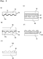
- the nano-imprinting method is a technique capable of transferring a pattern in nano-meter order by sandwiching a resin between a mold and a substrate, and basically is composed of the following four steps of: (i) coating with a resin layer (application of a resin layer), (ii) pressing with the mold, (iii) transferring of the pattern and (iv) releasing of the mold (mold-releasing).
- the nano-imprint method is excellent in that the nano-sized processing can be realized with such a simple process.
- the nano-imprint method devises or apparatuses used therefor are simple, the processing can be performed for a large area as well as a high throughput can be expected. Accordingly, the nano-imprint method is expected to be practiced not only in the field of semiconductor device but also in many fields such as storage media, optical members, biochips, etc.
- a mold for transferring a pattern having a line width of several tens of nanometers (nm) needs to be formed basically by exposing a resist on a silicon substrate and developing the resist to form a resist pattern (a pattern of a resist), with a lithography apparatus. Further, an electric current seed layer (current seed layer) made of a metal is formed on the resist pattern for performing electroforming (electroplating) of the mold by using the obtained resist pattern.
- the coating performance (coatability or coverage) of the current seed layer formed on the pattern by sputtering is lowered, which in turn causes such a state that the film thickness (thickness) of the obtained current seed layer is different or non-uniform among an upper portion, a side wall portion and a bottom portion of the resist pattern (the bottom portion being a substrate-exposure portion in which the substrate is exposed in a recessed portion in the pattern, namely in a trench).
- the formation of the current seed layer is progressed preferentially in the upper portion of the resist pattern, thereby causing such a problem that the opening of the trench is constricted or narrowed.
- Patent Literature 1 discloses a method for producing a mold for nano-imprint including the steps of:
- this method is capable of growing the electroforming film in unidirectional manner upwardly from the conductive surface at the bottom portion of the resist pattern without using a current seed layer, it is considered that any void is not present inside the mold for nano-imprint. Even with this method, however, the mold used in the nano-imprint method should be made with the lithography method, same as before.
- the inventors of the present invention disclose the following method in PATENT LITERATURE 2. Namely, a block copolymer solution containing a block copolymer satisfying a predetermined condition and a solvent is applied on a base member (the base member is coated with the block copolymer solution), and drying is performed for the applied block copolymer solution to form a micro phase separation structure of the block copolymer, thereby obtaining a master block (mold) in which a fine (minute) and irregular concave-convex pattern is formed. According to this method, it is possible to obtain the master block usable for the nano-imprint and the like by using a self-organizing phenomenon of the block copolymer, without using the lithography method.
- a mixture of a silicone-based polymer and a curing agent is dropped onto the obtained master block and then cured to obtain a transferred pattern. Then, a glass substrate coated with a curable resin is pressed to (against) the transferred pattern and the curable resin is cured by irradiation with an ultraviolet light. In this way, a diffraction grating in which the transferred pattern is duplicated is manufactured.
- an organic EL diode organic light-emitting diode obtained by stacking a transparent electrode, an organic layer, and a metal electrode on the diffraction grating has sufficiently high light emission efficiency, sufficiently high level of external extraction efficiency, as well as sufficiently low wavelength-dependence of light emission, sufficiently low directivity of light emission, and sufficiently high power efficiency.
- a step is required for removing one of polymers composing the block copolymer with the etching process, so as to obtain the concave-convex pattern after the formation of the micro phase separation structure of the block copolymer. Due to this removing step, one of the polymers is removed as portions at each of which the base member is exposed and the other of the polymers is remained to form the convex portions. However, the remaining convex portions have small area of contact with the surface of the base member, and thus easily drop off or detach from the surface of the base member.
- Patent Literature 2 Japanese Patent Literature 2
- Patent Literature 3 disclose forming a columnar-shaped micro domain structure, lamella-type micro domain structure, etc., by phase-separating a high polymer layer including a block copolymer of which molecular weight is relatively low. This method, however, removes one of the polymers by the etching, etc., for the patterning purpose.
- an object of the present invention is to provide a method for producing a mold for transferring a fine pattern suitable for mass-producing a substrate having a concave-convex structure such as a diffraction grating usable for a general-purpose item such as an organic EL element, a method for producing a substrate having a concave-convex structure by using the obtained mold, and a method for producing an organic EL element using the substrate having such concave-convex structure.
- Another object of the present invention is to produce a mold for transferring a fine pattern, a substrate having a concave-convex structure, and an organic EL element with a high throughput by using one of these producing methods.
- a method for producing a mold for transferring a fine pattern including:
- a volume ratio between the first and second polymer segments in the block copolymer is in a range of 4:6 to 6:4, in view of generating the horizontal cylinder structure.
- a content amount of the polyalkylene oxide is preferably in a range of 5 parts by mass to 70 parts by mass relative to 100 parts by mass of the block copolymer, in view of obtaining sufficient height (groove depth) of the concave-convex structure.
- number average molecular weight of the block copolymer is preferably not less than 500,000.
- any etching process is not necessary after the solvent phase-separation process (step).
- the first polymer segment composing the block copolymer may be polystyrene; the second polymer segment composing the block copolymer may be polymethyl methacrylate.
- the organic solvent may be one selected from the group consisting of chloroform, acetone, dichloromethane, and a mixed solvent of carbon bisulfide and acetone.
- a time for phase-separating the block copolymer under the presence of the vapor of the organic solvent may be in a range of 6 hours to 168 hours.
- the concave-convex structure appears on the surface.
- an average value of depth distribution of concavities and convexities of the concave-convex structure is in a range of 20 nm to 200 nm, preferably in a range of 30 nm to 150 nm; and that standard deviation of depth of the concavities and convexities is in a range of 10 nm to 100 nm, more preferably in a range of 15 nm to 75 nm.
- a primer layer is formed on the surface of the base member before coating the surface of the base member with the solution containing the block copolymer, which is composed of at least the first and second polymer segments, and the polyalkylene oxide.
- Mw/Mn molecular weight distribution of the block copolymer is preferably not more than 1.5, and difference in solubility parameter between the first and second polymer segments is in a range of 0.1 (cal/cm 3 ) 1/2 to 10 (cal/cm 3 ) 1/2 .
- a method for producing a diffraction grating including:
- a method for producing a diffraction grating including:
- a method for producing an organic EL element including: stacking a transparent electrode, an organic layer and a metal electrode successively on a concave-convex structure of a diffraction grating, produced by the above method of producing the diffraction grating, so as to form the organic EL element.
- a mold for transferring a fine pattern produced by the above method for producing the mold is provided.
- a seventh aspect of the present invention there is provided a method for producing an organic EL element.
- a method for producing a substrate having a concave-convex structure including: pressing a mold obtained by the above method for producing the mold onto a substrate coated with a concavity-convexity forming material, curing the concavity-convexity forming material, and removing the mold from the substrate so as to form the substrate having a concave-convex structure.
- a method for producing a substrate having a concave-convex structure including:
- a block copolymer film of which surface has a smooth and wave-like concave-convex structure and of which cross-sectional structure has a horizontal cylinder structure can be obtained by phase-separating the solution, which contains the block copolymer, with the organic solvent so as to cause the self-organization of the block copolymer.
- the etching step which has been required for forming the concave-convex structure becomes unnecessary, thereby realizing a simplified production process and lowering the possibility that any dirt (stain, soil, dust) and/or any foreign matter might adhere to the mold through the production process, as well.
- the surface property of a metal layer of the obtained mold is such that smooth concavities and convexities are distributed substantially uniformly, and that a resin is suppressed from remaining on a side of the mold when the block copolymer and the base member are released (peeled off) from the mold, thereby enhancing the releasing property (peeling property) of the mold. With this, any pattern defect is prevented from generating. Further, even in a case that the molecular weight of the block copolymer is as high as 500,000 or more, it is possible to form a mold having a desired concave-convex pattern in an ensured manner.
- a substrate having the concave-convex structure such as a diffraction grating diffracting a light of the visible region without any wavelength dependency and with low directivity, can be produced with a relatively low cost and with a high throughput.
- the mold-producing method mainly includes a step for preparing a solution of block copolymer (block copolymer solution), a step of coating a base member with the block copolymer solution (applying the block copolymer solution), a drying step, a solvent annealing step, a step of forming a seed layer, an electroforming step and a releasing step (peeling step).
- a substrate having the concave-convex structure according to the present invention is not limited to the optical substrate such as the diffraction grating substrate and is applicable also to a variety of substrates having various applications, as will be described later on.
- the block copolymer used for present invention includes at least a first polymer segment made of a first homopolymer and a second polymer segment made of a second homopolymer different from the fist homopolymer.
- the second homopolymer desirably has a solubility parameter which is higher than a solubility parameter of the first homopolymer by 0.1 (cal/cm 3 ) 1/2 to 10 (cal/cm 3 ) 1/2 .
- the difference in the solubility parameter between the first and second homopolymers is less than 0.1 (cal/cm 3 ) 1/2 , it is difficult to form a regular micro phase separation structure of the block copolymer.
- the difference exceeds 10 (cal/cm 3 ) 1/2 , it is difficult to prepare a uniform solution of the block copolymer.
- Examples of monomers serving as raw materials of homopolymers usable as the first homopolymer and second homopolymer include styrene, methylstyrene, propylstyrene, butylstyrene, hexylstyrene, octylstyrene, methoxystyrene, ethylene, propylene, butene, hexene, acrylonitrile, acrylamide, methyl methacrylate, ethyl methacrylate, propyl methacrylate, butyl methacrylate, hexyl methacrylate, octyl methacrylate, methyl acrylate, ethyl acrylate, propyl acrylate, butyl acrylate, hexyl acrylate, octyl acrylate, methacrylic acid, acrylic acid, hydroxyethyl methacrylate, hydroxyethyl acrylate,
- styrene, methyl methacrylate, ethylene oxide, butadiene, isoprene, vinylpyridine, and lactic acid are preferably used from the viewpoints that the formation of phase separation easily occurs, and that concavities and convexities of the concave-convex structure are easily formed by an etching.
- examples of a combination of the first homopolymer and the second homopolymer may include combinations of two selected from the group consisting of a styrene-based polymer (more preferably, polystyrene), polyalkyl methacrylate (more preferably, polymethyl methacrylate), polyethylene oxide, polybutadiene, polyisoprene, polyvinylpyridine, and polylactic acid.
- a styrene-based polymer more preferably, polystyrene
- polyalkyl methacrylate more preferably, polymethyl methacrylate
- polyethylene oxide polybutadiene
- polyisoprene polyvinylpyridine
- polylactic acid polylactic acid
- a combination of the styrene-based polymer and polyalkyl methacrylate, a combination of the styrene-based polymer and polyethylene oxide, a combination of the styrene-based polymer and polyisoprene, a combination of the styrene-based polymer and polybutadiene are more preferable, and the combination of the styrene-based polymer and polymethyl methacrylate, the combination of the styrene-based polymer and polyisoprene, the combination of the styrene-based polymer and polybutadiene are particularly preferable.
- a combination of polystyrene (PS) and polymethyl methacrylate (PMMA) is further preferable from the viewpoint of obtaining a preferable number average molecular weight (Mn) of the block copolymer.
- the number average molecular weight (Mn) of the block copolymer is preferably not less than 500,000, and more preferably not less than 1,000,000, and particularly preferably in a range of 1,000,000 to 5,000,000.
- the domain size of the block copolymer increases as the molecular weight thereof increases. In a case that the number average molecular weight is less than 500,000, the average pitch of the concavities and convexities formed by the micro phase separation structure of the block copolymer is so small that the average pitch of the concavities and convexities of the obtained diffraction grating becomes insufficient.
- the diffraction grating needs to diffract illumination light over a range of wavelength of the visible region, and thus the average pitch is desirably in a range of 100 nm to 1,500 nm, more desirably in a range of 200 nm to 1,200 nm.
- the number average molecular weight (Mn) of the block copolymer is preferably not less than 500,000.
- the molecular weight distribution (Mw/Mn) of the block copolymer is preferably not more than 1.5, and is more preferably in a range of 1.0 to 1.35. In a case that the molecular weight distribution exceeds 1.5, it is difficult to form the regular micro phase separation structure of the block copolymer.
- the number average molecular weight (Mn) and the weight average molecular weight (Mw) of the block copolymer are values measured by the gel permeation chromatography (GPC) and converted to the molecular weights of standard polystyrene.
- the volume ratio between the first polymer segment and the second polymer segment is in a range of 4:6 to 6:4 in order to generate a horizontal cylinder structure by self-organization or assembly (to be described later on), and is preferably about 5:5.
- the volume ratio is out of the above-described range, it is difficult to form a concave-convex pattern (concavity and convexity pattern) owing to the horizontal cylinder structure (to be described later on) and there is a tendency that a globular or spherical structure or vertical cylinder structure appears.
- the block copolymer solution used in the present invention is prepared by dissolving the block copolymer in a solvent.
- the solvent include aliphatic hydrocarbons such as hexane, heptane, octane, decane, and cyclohexane; aromatic hydrocarbons such as benzene, toluene, xylene, and mesitylene; ethers such as diethyl ether, tetrahydrofuran, and dioxane; ketones such as acetone, methyl ethyl ketone, isophorone, and cyclohexanone; ether alcohols such as butoxyethyl ether, hexyloxyethyl alcohol, methoxy-2-propanol, and benzyloxyethanol; glycol ethers such as ethylene glycol dimethyl ether, diethylene glycol dimethyl ether, triglyme, propylene glycol monomethyl ether, and propylene
- the percentage content of the block copolymer in the block copolymer solution is preferably in a range of 0.1% by mass to 15% by mass, and more preferably in a range of 0.3% by mass to 5% by mass, relative to 100% by mass of the block copolymer solution.
- the block copolymer solution further contains polyalkylene oxide as a different homopolymer (a homopolymer other than the first homopolymer and the second homopolymer in the block copolymer contained in the solution: for example, in a case that the combination of the first homopolymer and the second homopolymer in the block copolymer is the combination of polystyrene and polymethyl methacrylate, the different homopolymer may be any kind of homopolymer other than polystyrene and polymethyl methacrylate).
- the depth of the concavities and convexities formed by the micro phase separation structure of the block copolymer can be increased.
- polyalkylene oxide polyethylene oxide or polypropylene oxide is more preferable, and polyethylene oxide is particularly preferable.
- polyethylene oxide one represented by the following formula is preferable: HO-(CH 2 -CH 2 -O) n -H [in the formula, "n" represents an integer in a range of 10 to 5,000 (more preferably an integer in a range of 50 to 1,000, and further preferably an integer in a range of 50 to 500)].
- the number average molecular weight (Mn) of polyalkylene oxide is preferably in a range of 460 to 220,000, and is more preferably in a range of 2,200 to 46,000. In a case that the number average molecular weight is less than the lower limit, the molecular weight is so low that polyalkylene oxide is liquid at room temperature, is easily separated out and precipitates; in another case that the number average molecular weight exceeds the upper limit, the synthesis of such polyalkylene oxide is difficult.
- the molecular weight distribution (Mw/Mn) of polyalkylene oxide is preferably not more than 1.5, and more preferably in a range of 1.0 to 1.3. In a case that the molecular weight distribution exceeds the upper limit, the uniformity of shape of the micro phase separation is less likely to be maintained.
- Mn and Mw are values measured by the gel permeation chromatography (GPC) and converted to molecular weights of standard polystyrene.
- the combination of the first homopolymer and the second homopolymer in the block copolymer is the combination of polystyrene and polymethyl methacrylate (polystyrene-polymethyl methacrylate).
- polystyrene-polymethyl methacrylate block copolymer and polyalkylene oxide such as polyethylene oxide in combination as described above, the orientation in the vertical direction is further improved, thereby making it possible to further increase the depths of the concavities and convexities on the surface, and to shorten the solvent annealing process time during the production.
- the content of polyalkylene oxide is preferably in a range of 1 part by mass to 100 parts by mass, and particularly preferably in a range of 5 parts by mass to 100 parts by mass, relative to 100 parts by mass of the block copolymer.
- the content of polyalkylene oxide is further preferably in a range of 5 parts by mass to 70 parts by mass. In a case that the content of polyalkylene oxide is less than 5 parts by mass, the effect obtained by containing polyalkylene oxide becomes insufficient.
- the total percentage content of polyalkylene oxide and the different homopolymer in the block copolymer solution is preferably in a range of 0.1 % by mass to 15% by mass, and more preferably in a range of 0.3% by mass to 5% by mass, in the block copolymer solution.
- the total percentage content is less than the lower limit, it is difficult to uniformly apply the solution on a base member (coat a base member with the solution) to attain a film of which thickness is sufficient to obtain a necessary film thickness.
- the total percentage content exceeds the upper limit, it is relatively difficult to prepare a solution in which polyalkylene oxide and the different homopolymer are uniformly dissolved in the solvent.
- block copolymer solution may further contain another homopolymer different from polyalkylene oxide, a surfactant, an ionic compound, an anti-foaming agent, a leveling agent, and the like.
- the another homopolymer may be contained at a ratio in a range of 1 part by mass to 100 parts by mass, relative to 100 parts by mass of the block copolymer, similarly to polyalkylene oxide.
- the content of the surfactant is preferably not more than 10 parts by mass, relative to 100 parts by mass of the block copolymer.
- the ionic compound is used, the content of the ionic compound is preferably not more than 10 parts by mass, relative to 100 parts by mass of the block copolymer.
- the block copolymer solution prepared as described above is applied on a base member 10 (a base member 10 is coated with the block copolymer solution) to form a thin film 30.
- the base member 10 is not especially limited, and includes, for example, resin substrates of resins such as polyimide, polyphenylene sulfide (PPS), polyphenylene oxide, polyether ketone, polyethylene naphthalate, polyethylene terephthalate, polyarylate, triacetyl cellulose, and polycycloolefin; inorganic substrates such as glass, octadecyldimethyl chlorosilane (ODS) treated glass, octadecyl trichlorosilane (OTS) treated glass, organo silicate treated glass, glass substrates treated with a silane coupling agent, and silicon substrates; and substrates of metals such as aluminum, iron, and copper.
- resin substrates of resins such as polyimide, polyphenylene sulfide (PPS), polyphenylene oxide, polyether ketone, polyethylene naphthalate, polyethylene terephthalate, polyarylate, triacetyl cellulose, and
- the base member 10 may be subjected to a surface treatment such as an orientation treatment, etc.
- the organo silicate treated glass can be prepared by coating a glass with a methyl isobutyl ketone (MIBK) solution of methyl trimethoxysilane (MTMS) and 1,2-bis(trimethoxysilyl) ethane (BTMSE), and then performing heating process to the glass coated with the MIBK solution.
- MIBK methyl isobutyl ketone
- MTMS methyl trimethoxysilane
- BTMSE 1,2-bis(trimethoxysilyl) ethane
- each of the octadecyldimethyl chlorosilane treated glass and octadecyl trichlorosilane treated glass can be prepared by such a method including immersing a glass in a heptane solution of one of the octadecyldimethyl chlorosilane and octadecyl trichlorosilane, and washing out the unreacted portion from the glass.
- the method for applying the block copolymer solution on the base member is not particularly limited; it is allowable to employ, for example, the spin coating method, spray coating method, dip coating method, dropping method, gravure printing method, screen printing method, relief printing method, die coating method, curtain coating method, ink-jet method, etc., as the method for applying the block copolymer solution.
- the thickness of the thin film 30 of the block copolymer is preferably within a range which allows the thickness of a dried coating film, as will be described later, to be in a range of 10 nm to 3,000 nm, and more preferably within a range which allows the thickness of the dried coating film to be in a range of 50 nm to 500 nm.
- the thin film 30 on the base member 10 is dried.
- the drying can be performed in the ambient atmosphere.
- the temperature for drying the thin film 30 is not particularly limited, provided that the solvent can be removed from the thin film 30.
- the drying temperature is preferably in a range of 10 degrees Celsius to 200 degrees Celsius, and more preferably in a range of 20 degrees Celsius to 100 degrees Celsius. Note that in some cases, the drying step starts the formation of micro phase separation structure of the block copolymer, which results in appearance of concavities and convexities on the surface of the thin film 30 during the drying step.
- the solvent annealing process (solvent phase-separation process) is performed for the thin film 30 under atmosphere of the vapor of an organic solvent so as to form a phase separation structure of the block copolymer inside the thin film 30.
- the self-organization of the block copolymer is advanced such that the block copolymer undergoes micro phase separation into a portion corresponding to a first polymer segment 32 and a portion corresponding to a second polymer segment 34, thereby generating a horizontal cylinder structure, as shown in Fig. 1(B) .
- horizontal cylinder structure means a structure wherein the first polymer segment or the second polymer segment is self-organized such that the first or second polymer segment extends (is oriented) in a form of cylinders in a direction along the surface, of the base member, coated with the solution of the block copolymer.
- vertical cylinder structure means a structure wherein the first polymer segment or the second polymer segment is self-organized such that the first or second polymer segment extends (is oriented) in a form of cylinders in a direction substantially vertical to the surface, of the base member, coated with the solution of the block copolymer.
- SAXS small-angle X-ray scattering
- the solvent annealing process can be practiced by providing atmosphere of the vapor of organic solvent (organic solvent vapor) inside a tightly sealable container such as a desiccator, and by exposing the thin film 30 as the objective under this atmosphere.
- the concentration of the organic solvent vapor is preferably high for the purpose of promoting the phase separation of the block copolymer, is preferably saturated vapor pressure.
- the concentration of the organic solvent vapor is relatively easy to control.
- the saturated vapor pressure of chloroform is known to be in a range of 0.4 g/l to 2.5 g/l at room temperature (0 degrees Celsius to 45 degrees Celsius).
- the process time (process time period) of the solvent annealing process can be in a range of 6 hours to 168 hours, preferably in a range of 12 hours to 48 hours, more preferably in a range of 12 hours to 36 hours.
- the concave-convex shape collapses (becomes blunt); in a case that the process time is too short, the depth of the grooves in the concave-convex structure is shallow, and in a case that a diffraction grating is produced by using the mold, the diffraction effect of the diffraction grating is not sufficient.
- the organic solvent to be used in the solvent annealing process is preferably an organic solvent of which boiling point is in a range of 20 degrees Celsius to 120 degrees Celsius; it is possible to use, for example, chloroform, dichloromethane, toluene, tetrahydrofuran (THF), acetone, carbon disulfide, and mixture solvents thereof. Among these solvents, chloroform, dichloromethane, acetone, a mixture solvent of acetone/carbon disulfide are preferable.
- the solvent annealing may be performed at the ambient temperature in a range of 0 degrees Celsius to 45 degrees Celsius. In a case that the ambient temperature is higher than 45 degrees Celsius, the concave-convex structure formed in the thin film become blunt and easily collapses. In an environment lower than 0 degrees Celsius, the organic solvent hardly evaporates, and the phase separation of the block copolymer is hard to occur.
- the solvent annealing process causes the block copolymer to undergo the phase separation into the horizontal cylinder structure.
- the mixing ratio between the first homopolymer and the second homopolymer constructing the block copolymer is even (5:5) or approximately even, a phase separation structure of the lamella type appears by the thermal annealing process; in a case that the mixing ratio is approximately 3:7, the cylinder structure appears by the thermal annealing process; and in a case that the mixing ratio is approximately 2:8, the spherical structure appears by the thermal annealing process.
- the inventors found out that, when performing the solvent annealing process according to the present invention, the phase separation occurs while generating a cylinder structure in the horizontal direction even in a case that the mixing ratio of the first homopolymer and the second homopolymer constructing the block copolymer is in a range of 40:60 to 60:40. Although the reason for the above phenomenon is not clear, the inventors consider that as the organic solvent permeates into one of the homopolymers and causes one of the homopolymers to swell, which in turn creates such a situation that the apparent volume ratio between the first and second homopolymers is different from the actual mixing ratio between the first and second homopolymers.
- a first homopolymer 32 is present in a layer of a second homopolymer 34, and is oriented in a form of cylinders extending in a direction substantially parallel to the surface of the base member 10, as shown in Fig. 1(B) .
- a surface (top) layer portion, of the second homopolymer 34, under (inside) which the first homopolymer 32 is present is smoothly raised to form a wave-like shape.
- the cylinder-like arrangement in which the first homopolymer 32 is oriented in the form of cylinders extending in the direction substantially parallel to the surface of the base member 10 is formed in a plurality of layers (plurality of tiers or stages) in a direction (height direction) vertical to the surface of the base member 10 (see Figs. 8A and 8B which will be described later on).
- the raised wave-like structure can be used as it is as a concave-convex pattern of an optical substrate such as a diffraction grating. Accordingly, unlike the case of phase separation by the thermal annealing, there is no need to remove one of the homopolymers by the etching after the phase separation.
- a vertical cylinder structure or a spherical structure may be included in a part of the horizontal cylinder structure.
- the etching process is not necessary in the solvent annealing process, the patterning process for the mold can be simplified. Further, although the etching process normally involves the following problems, the mold-producing method of the present invention does not involve such problems. Namely, when performing the etching process, any projecting portion is easily generated in the remaining homopolymer pattern, the value of kurtosis (to be described later on) is small, and any cross-sectional shape having an overhang portion is easily generated. Accordingly, in the electroforming process performed thereafter, the plating metal is easily drawn to a projection portion and/or a projected corner (edge) of the object, and is less likely to be drawn to a recessed portion or a dented portion of the object.
- a seed layer to be deposited before the electroplating process is also less likely to adhere to a portion having such a complicated structure. Due to the situations described above, any defect is likely to occur in the pattern due to the etching process. Furthermore, any stain and/or debris (dust) are/is easily generated on the mold in the etching process due to the usage of etching liquid and/or the removal of one of the homopolymers constructing the block copolymers.
- the necessity for the etching process is eliminated, thereby solving the above-described problems associated with the etching and making it possible to obtain a mold which has a reliable concave-convex pattern and to which little foreign matter adheres and to obtain an optical substrate such as a diffraction grating produced based on the mold. Accordingly, the optical substrate such as the diffraction grating can be produced with a high throughput and in a simple process.
- the surface shape defined by the polymer segment 34 through the solvent annealing process is constructed of a relatively smooth and sloped (inclined) surface, as conceptually shown in Fig. 1 (B) , forming a wave-like shape (referred to as "wave-like structure" in the present application, as appropriate) in a direction upward from the base member.
- wave-like structure 38 there is no overhang, and thus the wave-like structure is duplicated into an inverted pattern in a metal layer accumulated on the wave-like structure 38, thereby allowing the metal layer to be easily releasable (peelable).
- the base member 10, which has the wave-like structure 38 obtained in such a manner, can be used as a master (mold) for transfer in a subsequent step.
- the average pitch of the concavities and convexities representing the wave-like structure 38 is preferably in a range of 100 nm to 1,500 nm, and more preferably in a range of 200 nm to 1,200 nm. In a case that the average pitch of the concavities and convexities is less than the lower limit, the pitch is too small relative to the wavelength of a visible light, and thus any required diffraction of the visible light is less likely to occur in a diffraction grating obtained by use of such a master (master block).
- the average pitch of the concavities and convexities means an average value of the pitch of concavities and convexities in a case of measuring the pitch of the concavities and convexities (spacing distance between adjacent convex portions or spacing distance between adjacent concave portions) on a surface of a curable resin layer. Further, such an average value of the pitch of concavities and convexities is obtained as follows.
- a concavity and convexity analysis image is obtained by measuring the shape of the concavities and convexities on the surface by using a scanning probe microscope (for example, a scanning probe microscope manufactured by Hitachi High-Tech Science Corporation, under the product name of "E-sweep", or the like), then the distances between randomly selected concave portions or convex portions adjacent to each other are measured at not less than 100 points in the concavity and convexity analysis image, and then the average of the distances is calculated and is determined as the average value of the pitch of concavities and convexities.
- a scanning probe microscope for example, a scanning probe microscope manufactured by Hitachi High-Tech Science Corporation, under the product name of "E-sweep", or the like
- the average value of depth distribution of concavities and convexities representing the concave-convex structure 38 is preferably in a range of 20 nm to 200 nm, more preferably in a range of 30 nm to 150 nm.
- the average value of depth distribution of the concavities and convexities is less than the lower limit, the height is not sufficient with respect to the wavelength of the visible light, thus resulting in insufficient diffraction; in a case that the average value exceeds the upper limit and that the obtained diffraction grating is used as an optical element on the light extraction port side of an organic EL element, the organic EL element tends to be easily destructed and the life thereof tends to be shortened due to the heat generation occurring when the electric field distribution in the organic layer becomes non-uniform, causing the electric field to concentrate on a certain position or area in the organic layer.
- the average value (m) of the depth distribution of concavities and convexities is represented by the following formula (I):
- the heating process blunts the formed concave-convex structure in some case.
- the heating process is not necessarily indispensable.
- the heating process is useful, for example, in such a case that any projection portion is formed, due to any reason, at a portion on the surface of the concave-convex structure after the solvent annealing process and/or such a case that the heating process is needed for adjusting the periodicity and/or height of the concave-convex structure.
- the heating temperature can be, for example, not less than the glass-transition temperatures of the first and second homopolymer segments 32, 34, such as a temperature not less than the glass-transition temperature of each of the first and second homopolymers 32, 34 and not more than a temperature that is higher than the glass-transition temperature by 70 degrees Celsius.
- the heating process can be performed in the ambient atmosphere by using an oven, etc.
- a seed layer 40 functioning as an electroconductive layer for a subsequent electroforming process is formed on the surface of the wave-like structure 38 of the master obtained as described above.
- the seed layer 40 can be formed by the non-electrolytic plating, sputtering, or vapor deposition.
- the thickness of the seed layer 40 is preferably not less than 10 nm, and more preferably not less than 20 nm to uniformize the current density during the subsequent electroforming process, thereby making the thickness of the metal layer accumulated by the subsequent electroforming process to be constant.
- the material of the seed layer it is possible to use, for example, nickel, copper, gold, silver, platinum, titanium, cobalt, tin, zinc, chrome, gold-cobalt alloy, gold-nickel alloy, boron-nickel alloy, solder, copper-nickel-chromium alloy, tin-nickel alloy, nickel-palladium alloy, nickel-cobalt-phosphorus alloy, or alloy thereof.
- a metal layer 50 is accumulated on the seed layer 40 by the electroforming (electroplating), as shown in Fig. 1(D) .
- the whole thickness of the metal layer 50 including the thickness of the seed layer 40 can be, for example, in a range of 10 ⁇ m to 3,000 ⁇ m.
- the material of the metal layer 50 to be accumulated by the electroforming it is possible to use any of metal species as described above which can be used as the seed layer 40.
- Nickel is preferable in view of the wear resistance and releasing property as the mold. In this case, nickel is also preferably used for the seed layer 40.
- the current density during the electroforming may be, for example, in a range of 0.03 A/cm 2 to 10 A/cm 2 for suppressing bridge to form a uniform metal layer and in view of shortening of electroforming time (duration of electroforming time).
- the formed metal layer 50 desirably has appropriate hardness and thickness.
- a diamond like carbon (DLC) processing or a Cr plating processing treatment may be performed on the surface of the metal layer formed by the electroforming in order to improve the hardness of the metal layer.
- the surface hardness of the metal layer may be improved by further performing the heating process of the metal layer.
- the metal layer 50 including the seed layer obtained as described above is released (peeled off) from the base member having the concave-convex structure to thereby obtain a mold as a father die.
- the metal layer 50 may be released physically, or the first and second homopolymer and the remaining block copolymer may be dissolved to be removed by using an organic solvent which dissolves the first and second homopolymer and the remaining block copolymer, such as toluene, tetrahydrofuran (THF), and chloroform.
- a polymer portion or portions 60 of the polymer remain(s) on the mold in some cases, as shown in Fig. 1(E) .
- each of the polymer portions 60 remaining on the mold can be removed by cleaning.
- the wet cleaning or dry cleaning can be used.
- the remaining polymer portions 60 can be removed by performing the cleaning with an organic solvent such as toluene and tetrahydrofuran, a surfactant, or an alkaline solution. In a case that the organic solvent is used, ultrasonic cleaning may be carried out.
- the remained polymer portions 60 may be removed by performing electrolytic cleaning.
- the remaining polymer portions 60 can be removed by ashing using ultraviolet light and/or plasma.
- the wet cleaning and the dry cleaning may be used in combination.
- a rinse process with pure water or purified water may be performed, and then ozone irradiation may be carried out after a drying process.
- a mold 70 having a desired concave-convex structure as shown in Fig. 1(F) is obtained.
- a mold-release treatment may be performed for the mold 70 so as to improve the releasability of the mold from the resin.
- the mold-release treatment a manner to decrease the surface energy is commonly used.
- the mold-release treatment includes, for example, a method in which a concave-convex surface 70a of the mold 70 is coated with a mold-release agent 72 such as a fluorine-based material and a silicone resin-based mold-release agent, as shown in Fig. 2(A) , a method in which the surface is subjected to a treatment using a fluorine-based silane coupling agent, a method in which a film of a diamond like carbon is formed on the surface, etc.
- a substrate (or a master block) having a concave-convex structure transferred thereon is produced by transferring the concave-convex structure (pattern) of the mold to a concave-convex forming material layer which is formed of an organic material such as a resin or an inorganic material such as a sol-gel material.
- the shape of the mold 70 may be changed suitably to the transfer.
- the mold 70 may be wound around the outer circumferential surface of a cylindrical body as a roll-shaped mold (transfer process using the roll-shaped mold will be described in detail later on).
- the concave-convex forming material to which the concave-convex structure is to be transferred is a resin layer.
- a supporting substrate 90 is coated with a curable resin to form a resin layer 80, and then the resin layer 80 is cured while the concave-convex structure of the mold 70 is being pressed against the resin layer 80, as shown in Fig. 2(B) .
- the supporting substrate 90 examples include a base member made of a transparent inorganic material such as glass; a base member made of a resin such as polyethylene terephthalate (PET), polyethylene naphthalate (PEN), polycarbonate (PC), cycloolefin polymer (COP), polymethyl methacrylate (PMMA) or polystyrene (PS); a stacked base member having a gas barrier layer made of an inorganic substance such as SiN, SiO 2 , SiC, SiO x N y , TiO 2 , or Al 2 O 3 formed on the surface of a base member made of any one of the above-described resins; and a stacked base member formed by alternately stacking a base member made of any one of the above-described resins and a gas barrier layer made of any one of the above-described inorganic substances.
- a base member made of a transparent inorganic material such as glass
- a base member made of a resin such as polyethylene terephthalate
- the thickness of the supporting substrate 90 may be within a range of 1 ⁇ m to 500 ⁇ m.
- an elongated (lengthy) sheet-shaped substrate having flexibility is preferably used as the supporting substrate 90, as will be described later on. Note that although the supporting substrate 90 is desirably transparent depending on the usage, the supporting substrate 90 needs not be transparent in a case of using the resin layer 80 having the concave-convex structure transferred thereon is used again as the mold (master block).
- the concave-convex forming material examples include curable resins including a variety of kinds of UV curable resin such as epoxy resin, acrylic resin, urethane resin, melamine resin, urea resin, polyester resin, phenol resin, and cross-linking type liquid crystal resin.
- the thickness of the curable resin is preferably in a range of 0.5 ⁇ m to 500 ⁇ m. In a case that the thickness is less than the lower limit, heights of the concavities and convexities formed on the surface of the cured resin layer are more likely to be insufficient. In a case that the thickness exceeds the upper limit, the effect of volume change of the resin which occurs upon curing is likely to be so large that the formation of the shape of the concavities and convexities tends to be unsatisfactory.
- the condition for curing a concave-convex forming material such as the curable resin varies depending on the kind of the resin used.
- the curing temperature is preferably in a range of the room temperature to 250 degrees Celsius
- the curing time is preferably in a range of 0.5 minutes to 3 hours.
- the curable resin is cured by being irradiated with energy ray such as ultraviolet light or electron beam.
- energy ray such as ultraviolet light or electron beam.
- the amount of the irradiation is preferably in a range of 20 mJ/cm 2 to 5 J/cm 2 .
- the method for detaching the mold 70 is not limited to a mechanical releasing method, and any known method can be adopted as the detaching method.
- a releasing roll peeling roll
- a resin film structure 100 in which the cured rein layer 80 having the concavities and convexities is formed on the supporting substrate 90 may be used, as it is, as the diffraction grating.
- the resin film structure 100 further as a mold to produce a structure constructed of an organic material such as a resin or a structure constructed of an inorganic material such as a sol-gel material, and to use either of the structures as a diffraction grating, as will be described later on.
- the mold-producing method according to the present invention can be used not only for producing a diffraction grating provided on the light extraction port side of the organic EL element but also for producing an optical component having a minute or fine pattern usable for various devices.
- the mold-producing method according to the present invention can be used to produce a wire grid polarizer, an antireflection film, a liquid crystal display, a touch panel or an optical element for providing the light confinement effect in a solar cell by being placed on the photoelectric conversion surface side of the solar cell.
- the resin film structure 100 having a desired pattern can be obtained.
- the resin film structure 100 obtained through the transfer process of the mold as described above is used as the master block; another transparent supporting substrate 92 is coated with a curable resin layer 82 and the curable resin layer 82 is cured while the resin film structure 100 is being pressed against the curable resin layer 82, as shown in Fig. 2(D) , similar to a case in which the resin film structure 100 is formed.
- the resin film structure 100 is released from the curable resin layer 82 which has been cured, and thus a replica 110 as another resin film structure as shown in Fig.
- 2(E) can be obtained. Further, it is allowable to produce a replica having the inverted pattern of the replica 110 by performing the above transfer step using the replica 110 as a master and/or to form a sub-replica by repeating the above transfer step again using the replica having the inverted pattern as the master block.
- a roll processing apparatus 170 shown in Fig. 4 forms a concave-convex pattern on a coating film applied (formed) on an elongated (long-length) substrate film 180 to thereby produce a film-shaped substrate 180a.
- the roll processing apparatus 170 is mainly provided with a transporting system 186 configured to transport the substrate film (base member) 180; a die coater 182 configured to coat the substrate film 180, which is being transported, with a concave-convex forming material; a metallic roll 190 located on the downstream of the die coater 182 and configured to transfer a pattern; and an irradiation light source 185 which is disposed to face the metallic roll 190 with the substrate film 180 being intervened between the irradiation light source 185 and the metallic roll 190, and which is configured to irradiate an UV light onto the substrate film 180.
- a transporting system 186 configured to transport the substrate film (base member) 180
- a die coater 182 configured to coat the substrate film 180, which is being transported, with a concave-convex forming material
- a metallic roll 190 located on the downstream of the die coater 182 and configured to transfer a pattern
- an irradiation light source 185 which is disposed
- the transporting system 186 for transporting the substrate film 180 has a film feeding roll 172 configured to feed the substrate film 180; a nip roll 174 and a releasing roll 176 arranged respectively on the upstream and the downstream of the metallic roll 190 and configured to urge the substrate film 180 toward the metallic roll 190; a take-up roll (winding roll) 187 configured to take up (wind up) a substrate film 180a having the pattern transferred thereon; and a plurality of transporting rolls 178 configured to transport the substrate film 180.
- the metallic roll 190 a roll-shaped mold obtained by winding the mold 70 (see Fig. 1(F) ), which has been prepared in advance, around the outer circumferential surface of a cylindrical body.
- the roll processing apparatus 170 is used to obtain a film-shaped substrate having a pattern of the metallic roll 190 transferred thereon, with the following process.
- the substrate film 180 wound around the film feeding roll 172 in advance is fed toward the downstream by the rotation of the film feeding roll 172, the film take-up roll 187, etc.
- the die coater 182 coats a surface of the substrate film 180 with a concave-convex forming material 184, thereby forming a coating film having a predetermined thickness.
- the coating film on the substrate film 180 is pressed against the outer circumferential surface of the metallic roll 190 by the nip roll 174, thereby the pattern on the outer circumferential surface of the metallic roll 190 is transferred to the coating film.
- the coating film is irradiated with the UV light from the irradiation light source 185, thereby the concave-convex forming material 184 is cured.
- the wavelength of the UV light is different depending on the kind or property of the concave-convex forming material 184, the wavelength is generally in a range of 200 nm to 450 nm; the irradiation amount of the UV light may be in a range of 10 mJ/cm 2 to 5 J/cm 2 .
- the substrate film 180 coated with the concave-convex forming material having the cured pattern is released away from the metallic roll 190 by the releasing roll 176, and then is took up (wound up) by the take-up roll 187. In such a manner, the elongated film-shaped substrate 180a can be obtained.
- the elongated film-shaped substrate 180a can be cut appropriately to be used as diffraction gratings.
- the elongated film-shaped substrate 180a can be used as a mold to transfer the concave-convex pattern again on a curable resin, a sol-gel material, etc.
- such an elongated film-shaped substrate 180a is obtained while being wound in a roll form, and thus is suitable as the mold used in a mass production process of an optical substrate (diffraction grating substrate), and has a suitable form for being transported to an apparatus for mass-producing the optical substrate.
- the film-shaped substrate can be stored or aged while being wound in a rolled form temporarily.
- sol-gel structure a structure having concavities and convexities made of a sol-gel material (hereinafter referred to as "sol-gel structure" as appropriate) by further using the obtained resin film structure 100, as shown in Fig. 2(C) , as the master block.
- sol-gel structure a sol-gel material
- a substrate-forming method for forming a substrate (structure) having a concave-convex pattern using the sol-gel material mainly includes: a solution preparation step S1 for preparing a sol; a coating step (application step) S2 for applying the prepared sol on a substrate (coating the substrate with the sol) to form a coating film; a drying step S3 for drying the coating film with which the substrate is coated; a transferring step S4 for pressing a mold having a transfer pattern formed thereon to the coating film; a releasing step S5 for releasing the mold from the coating film; and a main baking (main calcination) step S6 for subjecting the coating film to main baking.
- a solution preparation step S1 for preparing a sol
- a coating step (application step) S2 for applying the prepared sol on a substrate (coating the substrate with the sol) to form a coating film
- a drying step S3 for drying the coating film with which the substrate is coated
- a transferring step S4 for pressing a mold
- a sol is prepared to form a coating film, to which a pattern is to be transferred, by the sol-gel method (step S1 in Fig. 5 ).
- a sol of metal alkoxide sica precursor
- the silica precursor is exemplified by metal alkoxides including, for example, tetraalkoxide monomers such as tetramethoxysilane (TMOS), tetraethoxysilane (TEOS), tetra-i-propoxysilane, tetra-n-propoxysilane, tetra-i-butoxysilane, tetra-n-butoxysilane, tetra-sec-butoxysilane, and tetra-t-butoxysilane; trialkoxide monomers such as methyl trimethoxysilane, ethyl trimethoxysilane, propyl trimethoxysilane, isopropyl trimethoxysilane, phenyl trimethoxysilane, methyl triethoxysilane (MTES), ethyl triethoxysilane, propyl triethoxysilane, isopropyl trieth
- examples of the silica precursor include metal acetylacetonate, metal carboxylate, oxychloride, chloride, and mixtures thereof.
- the silica precursor is not limited to these.
- the examples of the metal species include Ti, Sn, Al, Zn, Zr, In, and mixtures thereof, but are not limited to these. It is also possible to use any appropriate mixture of precursors of the oxides of the above metals.
- the mixture ratio thereof can be 1:1, for example, in a molar ratio.
- This sol produces amorphous silica when caused to perform the hydrolysis and polycondensation reaction.
- An acid such as hydrochloric acid or an alkali such as ammonia is added in order to adjust the pH of the sol as a synthesis condition.
- the pH is preferably not more than 4 or not less than 10.
- Water may be added to perform the hydrolysis. An amount of water to be added can be not less than 1.5 times, with respect to metal alkoxide species, in the molar ratio.
- sol-gel material it is possible to use a material different from silica, and a material such as a Ti-based material, ITO (indium-tin oxide)-based material, Al 2 O 3 , ZrO 2 , ZnO, etc., may be used.
- a material such as a Ti-based material, ITO (indium-tin oxide)-based material, Al 2 O 3 , ZrO 2 , ZnO, etc., may be used.
- Examples of the solvent of the sol include alcohols such as methanol, ethanol, isopropyl alcohol (IPA), and butanol; aliphatic hydrocarbons such as hexane, heptane, octane, decane, and cyclohexane; aromatic hydrocarbons such as benzene, toluene, xylene, and mesitylene; ethers such as diethyl ether, tetrahydrofuran, and dioxane; ketones such as acetone, methyl ethyl ketone, isophorone, and cyclohexanone; ether alcohols such as butoxyethyl ether, hexyloxyethyl alcohol, methoxy-2-propanol, and benzyloxyethanol; glycols such as ethylene glycol and propylene glycol; glycol ethers such as ethylene glycol dimethyl ether, diethylene glycol dimethyl ether, and propylene
- polyethylene glycol polyethylene oxide, hydroxypropylcellulose, and polyvinyl alcohol for viscosity adjustment
- alkanolamine such as triethanolamine
- ⁇ -diketone such as acetylacetone, ⁇ -ketoester, formamid, dimetylformamide, and dioxane
- the substrate is coated with the sol prepared as described above (step S2 in Fig. 5 ).
- the substrate is preferably coated with the sol at a predetermined position while a plurality of substrates are being transported continuously.
- the coating method it is possible to adopt any coating method such as the bar coating method, spin coating method, spray coating method, dip coating method, die coating method, ink-jet method, etc.
- the die coating method, bar coating method and spin coating method are preferable because these methods are capable of performing the uniform coating of a substrate, which has a relatively large area, with the sol, and of quickly completing the coating before the sol turns into a gel.
- substrates made of inorganic materials such as glass, silica glass, and silicon substrates, or substrates made of resins such as polyethylene terephthalate (PET), polyethylene naphthalate (PEN), polycarbonate (PC), cycloolefin polymer (COP), polymethyl methacrylate (PMMA), polystyrene (PS), polyimide (PI), and polyarylate.
- PET polyethylene terephthalate
- PEN polyethylene naphthalate
- PC polycarbonate
- COP cycloolefin polymer
- PMMA polymethyl methacrylate
- PS polystyrene
- PI polyimide
- the substrate may be transparent or opaque, and a relatively hard substrate is preferable considering that a coating film (sol-gel material layer) is formed on the substrate and further a function layer is formed on the sol-gel material layer when the optical substrate is incorporated into a device.
- this substrate preferably is a substrate having the heat resistance and the weather resistance against the UV light, etc.
- the substrates made of the inorganic materials such as the glass, silica glass and silicon substrates are more preferable. Since the sol-gel material, with which the substrates made of the inorganic materials is to be coated, is made of the inorganic material, the difference in the refractive index between the substrates made of inorganic materials and the sol-gel material layer is small, and thus these substrates are preferable also in view of the capability for preventing any unintended refraction and/or reflection inside the optical substrate.
- a desired concave-convex pattern is formed with the sol-gel material layer in a subsequent or following step, and thus the surface of the substrate (including the surface treatment or the easy-adhesion layer in case that the surface treatment has been performed or the easy-adhesion layer has been formed) may be flat, and the substrate itself does not have the desired concave-convex pattern.
- Each of the substrates coated with the sol is transferred (transported) preferably as it is for the subsequent drying and transfer steps.
- the substrate is kept (held) in the atmosphere or under reduced pressure to evaporate the solvent in the coating film (hereinafter referred to also as "sol-gel material layer" as appropriate) applied on the substrate (step S3 in Fig. 5 ) to dry the coating film.
- the viscosity of the coating film is so low that the pattern cannot be transferred in the following transfer step; in a case that the holding time is too long, the polymerization reaction of the precursor is so advanced that the pattern cannot be transferred in the following transfer step.
- the holding time can be controlled by managing the transporting time during which the substrate is transported from a position where the coating of the substrate with the sol is performed to a position where the substrate is subjected to the following transfer step with the film-shaped substrate (mold).
- the holding temperature at which the temperature of the substrate is kept in the drying step is preferably a constant temperature in a range of 10 degrees Celsius to 100 degrees Celsius, and more preferably in a range of 10 degrees Celsius to 30 degrees Celsius.
- the gel reaction of the coating film is rapidly proceeds before the transfer step and thus is not desired; in a case that the holding temperature is lower than the lower limit of this range, the gel reaction of the coating film is slowly proceeds before the transfer step, which in turn lowers the productivity and thus not desired.
- the polymerization reaction of the precursor proceeds as the evaporation of the solvent proceeds, and the physical property such as the viscosity of the sol changes also in a short period of time.
- the evaporation amount of the solvent depends also on the amount of solvent (concentration of the sol) used in preparation of the sol.
- the sol contains the silica precursor
- the hydrolysis and polycondensation reaction of the silica precursor occur as the gel reaction, thereby producing alcohol in the sol via the dealcoholation reaction.
- a volatile solvent such as alcohol is used in the sol as the solvent.
- the sol contains the alcohol produced in the hydrolysis reaction and the alcohol present as the solvent, and the sol-gel reaction proceeds by removing these alcohols in the drying step. Therefore, it is desirable to adjust the holding time and/or holding temperature considering the gel reaction and the solvent used.
- the solvent in the sol evaporates just by holding the substrate as it is, and thus it is not necessarily indispensable to perform any active drying operation such as heating, air blowing, etc. It is sufficient just to hold the substrate formed with the coating film as it is for a predetermined period of time, to transfer the substrate for a predetermined period of time for the following step(s), etc. From this viewpoint, the drying step may be omitted.
- the film-shaped substrate 180a as the mold obtained in the roll processing apparatus 170 shown in Fig. 4 is pressed against the coating film with a pressing roll (laminating roll) so as to transfer the concave-convex pattern on the film-shaped substrate 180a to the coating film on the substrate (step S4 in Fig. 5 ).
- the concave-convex pattern of the film-shaped substrate 180a can be transferred to a coating film (sol) 142 on a substrate 140 by feeding the film-shaped substrate 180a between a pressing roll 122 and the substrate 140 transported immediately below the pressing roll 122, as shown in Fig. 6 .
- the film-shaped substrate 180a is made to cover the surface of the coating film 142 of the substrate 140 while the film-shaped substrate 180a and the substrate 140 are being transported in a synchronized manner.
- the pressing roll 122 is rotated while being pressed against the back surface of the film-shaped substrate 180a (surface on the opposite side to the other surface of the film-shaped substrate 180a having the concave-convex pattern formed thereon), thereby causing the film-shaped substrate 180a and the substrate 140 to tightly contact with each other while being advanced.
- the elongated film-shaped substrate 180a As the mold, the following advantages are obtained. Namely, with respect to a hard mold that is formed of metal, silica glass, etc., when any defect is found in the concave-convex pattern formed in the hard mold, it is possible to clean a defective portion of the concave-convex pattern at which the defect is located or to repair such defective portion (defect repairing). With this, it is possible to prevent any failure in the substrate 140 which would have been otherwise caused due to the defect transferred to the sol-gel side (the sol-gel material layer on the substrate 140). With respect to a film-shaped mold (soft mold), however, such cleaning and/or repair are not easy to perform therefor.
- the mold formed of the metal, silica glass, etc. is roll-shaped, and thus when any defect occurs in this mold due to, for example, clogging, etc., the transfer apparatus should be stopped immediately and the mold should be exchanged.
- the transfer with the film-shaped mold is performed while each of the parts of the film-shaped mold being made to correspond to each single glass substrate. Therefore, it is possible to mark any defective portion such as the clogging in the film-shaped mold in advance in an inspection stage, and the transporting operation of the glass substrate can be paused until the defective portion of the film-shaped mold pass the glass substrate. Accordingly, the occurrence of defective product can be lowered as a whole, thereby realizing enhanced throughput.
- the mold and the substrate are both hard. Therefore, when the pressing pressure for the mold is increased, any damage such as cracking or breakage of the substrate occurs; on the contrary, when the pressing pressure for the mold is decreased, the transfer of the concave-convex pattern is shallow, etc., and thus the pressing pressure is hard to adjust.
- the roll process using the pressing roll as described above has the following advantages over the pressing system. Namely, (i) since the period of time during which the mold and the coating film are brought in contact with each other in the roll process is short, it is possible to prevent any deformation of pattern due to the difference in coefficient of thermal expansion among the mold, the substrate, and a stage in which the substrate is placed, etc.; (ii) the productivity is improved owing to the roll process, and the productivity can be further improved by using the elongated film-shaped substrate (film-shaped mold); (iii) it is possible to prevent the generation of bubbles of gas in the pattern due to the bumping of the solvent in the sol or to prevent any trace or mark of gas from remaining; (iv) it is possible to reduce the transfer pressure and releasing force (peeling force) owing to the line contact with the substrate (coating film), thereby making it possible to easily handle a substrate with larger area; and (v) no bubble is included during the pressing.
- the producing method of the present invention uses the flexible, film-shaped substrate as the mold. Therefore, in a case of transferring the concave-convex pattern of the mold onto the sol-gel material layer formed on a relatively hard substrate, the concave-convex pattern of the mold can be pressed to the sol-gel material layer uniformly across the entire surface of the substrate. With this, the concave-convex pattern of the mold can be transferred faithfully to the sol-gel material layer, thereby making it possible to suppress any occurrence of lack of transfer, or any occurrence of defect, etc.
- the film-shaped substrate may be pressed against the coating film while the coating film is being heated.
- the heating may be performed via the pressing roll, or the coating film may be heated directly or indirectly from the side of the substrate.
- a heating mechanism may be provided inside the pressing roll (transfer roll), and any heating mechanism may be used.
- any heating mechanism that includes a heater inside the pressing roll is suitable, any separate heater different from the pressing roll may be provided. In either case, any pressing roll may be used, provided that the coating film can be pressed while being heated.
- the pressing roll is preferably a roll having a heat-resisting coating film, which is provided on a surface thereof and which is made of resin material such as ethylene-propylene-diene rubber (EPDM), silicone rubber, nitrile rubber, fluoro rubber, acrylic rubber, chloroprene rubber, etc.
- a support roll may be provided to face the pressing roll and to sandwich the substrate between the support roll and the pressing roll, or a support stand configured to support the substrate may be provided, for the purpose of resisting the pressure applied by the pressing roll.
- a heating temperature at which the coating film is heated during the transfer can be in a range of 40 degrees Celsius to 150 degrees Celsius.
- the heating temperature of the pressing roll can be similarly in a range of 40 degrees Celsius to 150 degrees Celsius.
- the heating temperature of the coating film or the pressing roll is less than 40 degrees Celsius, the mold cannot be expected to be released quickly from the coating film; in a case that the heating temperature exceeds 150 degrees Celsius, the solvent used evaporate rapidly, which in turn might result in the concave-convex pattern unsatisfactorily transferred.
- the coating film may be subjected to pre-baking. It is preferred to perform the pre-baking in a case that the transfer is performed without heating the coating film.
- the pre-baking promotes the gelation of the coating film to solidify the pattern, thereby making the pattern be less likely to be collapsed during the releasing.
- the heating is preferably performed at a temperature in a range of 40 degrees Celsius to 150 degrees Celsius in the atmosphere.
- the film-shaped substrate is released from the coating film (sol-gel material layer) after the pressing step or the pre-baking step (step S5 in Fig. 5 ). Since the roll process is used as described above, the releasing force may be smaller than that in a case of using a plate-shaped mold employed in the pressing system, and it is possible to easily release the mold (film-shaped substrate) from the coating film without leaving the coating film to be remained on the mold (film-shaped substrate). In particular, since the transfer is performed while heating the coating film, the reaction easily proceeds, and the mold can be easily released from the coating film immediately after the transfer. Further, a releasing roll (peeling roll) may be used for enhancing the releasability (peelability) of the mold. As shown in Fig.
- a peeling roll (releasing roll) 123 is provided on the downstream of the pressing roll 122, and the film-shaped substrate 180a is supported by the rotating peeling roll 123 while being urged by the peeling roll 123 toward the coating film 142.
- the film-shaped substrate 180a is peeled off from the coating film 142.
- the pre-baking and/or the heating of the coating film described above may be performed during a period of time when the film-shaped substrate 180a is adhered to the coating film 142. Further, in a case of using the peeling roll 123, the peeling off of the film-shaped substrate 180a from the coating film can be performed more easily by performing the peeling while the coating film is heated, for example, at a temperature in a range of 40 degrees Celsius to 150 degrees Celsius.
- the coating film 142 is subjected to the main baking (step S6 in Fig. 5 ).
- the hydroxyl group and the like contained in silica, etc. forming the coating film is desorbed or eliminated by the main baking to further strengthen the coating film.
- the main baking may be performed at a temperature in a range of 200 degrees Celsius to 1200 degrees Celsius for a duration of time about in a range of 5 minutes to 6 hours.
- the coating film is cured, and a substrate provided with a concave-convex pattern film which corresponds to the concave-convex pattern of the film-shaped substrate 180a is obtained, namely a substrate (diffraction grating) in which the sol-gel material layer having the concave-convex pattern is directly formed on the flat substrate is obtained.
- the sol-gel material layer is formed of silica
- the sol-gel material layer is amorphous, crystalline or in a mixture state of the amorphous and the crystalline, depending on the baking temperature and baking time.
- a film may be stacked or deposited, on the surface of the resin film structure 100 or the replica 110 (or sol-gel structure) having the concave-convex pattern formed thereon, by a gas phase method such as the vapor deposition or sputtering method.
- the adhesion between the resin (for example, a UV curable resin) and resin film structure 100 (the replica 110 or the sol-gel structure) can be lowered so as to allow the master block to be peeled off more easily.
- the vapor-deposited film include metals such as aluminum, gold, silver, platinum, and nickel; and metal oxides such as aluminum oxide.
- the thickness of such a vapor-deposited film is preferably in a range of 5 nm to 500 nm. In a case that the thickness is less than the lower limit, a uniform film is difficult to obtain, and thus that the effect of sufficiently lowering the adhesion is decreased.
- the shape of the master block is more likely to be blunt or dull.
- postcure may be conducted as appropriate by, for example, performing the irradiation with ultraviolet light again after the resin has been cured.
- the curable resins 80, 82 are applied on the supporting substrates 90, 92, respectively. It is allowable, however, to use a master block obtained by applying the curable resin directly on the surface of the mold 70 which is the original master block or on the surface of the cured resin layer 80, curing the applied curable resin and then detaching the cured curable resin.
- the master block instead of coating the surface of the master block with the resin, it is allowable to press the master block to a coating film of the resin and to cure the resin so as to obtain a concave-convex film which has concavities and convexities and formed of the cured resin, and to use the obtained concave-convex film of the cured resin as the master block.
- a substrate 140 on which a pattern made of a sol-gel material layer (coating film) 142 formed via the roll process explained with reference to Fig. 6 , is prepared.
- the substrate 140 is cleaned with a brush, etc., in order to remove any foreign matter adhered to the substrate 140, and an organic matter, etc. is removed with an alkaline cleaning agent and an organic solvent.
- a transparent electrode 93 is stacked on the sol-gel material layer 142 on the substrate 140 so as to maintain the concave-convex structure formed on the surface of the sol-gel material layer (coating film) 142.
- Examples of those usable as the material for the transparent electrode 93 include indium oxide, zinc oxide, tin oxide, indium-tin oxide (ITO) which is a composite material thereof; gold; platinum, silver; copper, etc. Among these materials, ITO is preferable from the viewpoint of the transparency and the electrical conductivity.
- the thickness of the transparent electrode 93 is preferably within a range of 20 nm to 500 nm. In a case that the thickness is less than the lower limit, the electrical conductivity is more likely to be insufficient. In a case that the thickness exceeds the upper limit, there is possibility that the transparency is so insufficient that the emitted EL light cannot be extracted to the outside sufficiently.
- the method for stacking the transparent electrode 93 it is possible to appropriately use any known method such as the vapor deposition method, sputtering method, spin coating method, etc.
- the sputtering method is preferably employed from the viewpoint of improving adhesion property.
- the transparent electrode 93 is coated with photoresist, followed by being exposed with an electrode mask pattern.
- etching is performed with a developing solution, thereby obtaining a transparent electrode having a predetermined pattern.
- the substrate is exposed to a high temperature of about 300 degrees Celsius.
- an UV ozone treatment is preferably performed.
- an organic layer 94 as shown in Fig. 7 is stacked on the transparent electrode 93.
- the organic layer 94 is not particularly limited, provided that the organic layer 94 is one usable as an organic layer of the organic EL element.
- the organic layer 94 any known organic layer can be used as appropriate.
- the organic layer 94 may be a stacked body of various organic thin films, and may be, for example, a stacked body of a hole transporting layer 95, a light emitting layer 96, and an electron transporting layer 97 as shown in Fig. 7 .
- examples of the material of the hole transporting layer 95 include aromatic diamine compounds such as phthalocyanine derivatives, naphthalocyanine derivatives, porphyrin derivatives, N,N'-bis(3-methylphenyl)-(1,1'-biphenyl)-4,4'-diamine (TPD), and 4,4'-bis[N-(naphthyl)-N-phenyl-amino]biphenyl( ⁇ -NPD); oxazole; oxadiazole; triazole; imidazole; imidazolone; stilbene derivatives; pyrazoline derivatives; tetrahydroimidazole; polyarylalkane; butadiene; and 4,4',4"-tris(N-(3-methylphenyl)N-phenylamino) triphenylamine (m-MTDATA).
- aromatic diamine compounds such as phthalocyanine derivatives, naphthalocyanine derivatives, porphyrin derivative
- the light emitting layer 96 is provided so that a hole injected from the transparent electrode 93 and an electron injected from a metal electrode 98 are recombined to emit light.
- the material usable as the light emitting layer 96 include: metallo-organic complex such as anthracene, naphthalene, pyrene, tetracene, coronene, perylene, phthaloperylene, naphthaloperylene, diphenylbutadiene, tetraphenylbutadiene, coumarin, oxadiazole, bisbenzoxazoline, bisstyryl, cyclopentadiene, and aluminum-quinolinol complex (Alq3); tri-(p-terphenyl-4-yl)amine; 1-aryl-2,5-di(2-thienyl) pyrrole derivatives; pyran; quinacridone; rubren; distyrylbenzene derivatives; distyryl
- light-emitting materials selected from the above compounds are mixed as appropriate and then are used.
- a material system generating emission of light from a spin multiplet such as a phosphorescence emitting material generating emission of phosphorescence, and a compound including, in a part of the molecules, a constituent portion formed by the above materials.
- the phosphorescence emitting material preferably includes heavy metal such as iridium.
- a host material having high carrier mobility may be doped with each of the light-emitting materials as a guest material to generate the light emission using the dipole-dipole interaction (Forster mechanism) or electron exchange interaction (Dexter mechanism).
- Examples of the material of the electron transporting layer 97 include heterocyclic tetracarboxylic anhydrides such as nitro-substituted fluorene derivatives, diphenylquinone derivatives, thiopyran dioxide derivatives, and naphthaleneperylene; and metallo-organic complex such as carbodiimide, fluorenylidene methane derivatives, anthraquino dimethane and anthrone derivatives, oxadiazole derivatives, and aluminum-quinolinol complex (Alq3).
- heterocyclic tetracarboxylic anhydrides such as nitro-substituted fluorene derivatives, diphenylquinone derivatives, thiopyran dioxide derivatives, and naphthaleneperylene
- metallo-organic complex such as carbodiimide, fluorenylidene methane derivatives, anthraquino dimethane and anthrone derivatives,
- oxadiazole derivatives it is also possible to use, as an electron transporting material, thiadiazole derivatives in which oxygen atoms of oxadiazole rings are substituted by sulfur atoms and quinoxaline derivatives having quinoxaline rings known as electron attractive group. Furthermore, it is also possible to use a polymeric material in which the above materials are introduced into a macromolecular chain or the above materials are made to be a main chain of the macromolecular chain. Note that the hole transporting layer 95 or the electron transporting layer 97 may also function as the light-emitting layer 96. In this case, the organic layer between the transparent electrode 93 and the metal electrode 98 is double-layered.
- a layer made of a metal fluoride or metal oxide such as lithium fluoride (LiF) or Li 2 O 3 , a highly active alkaline earth metal such as Ca, Ba, or Cs, an organic insulating material, or the like may be provided as an electron injection layer between the organic layer 94 and the metal electrode 98.
- the thicknesses of the hole transporting layer 95, the light emitting layer 96 and the electron transporting layer 97 are preferably within a range of 1 nm to 200 nm, a range of 5 nm to 100 nm, and a range of 5 nm to 200 nm, respectively.
- any known method such as the vapor deposition method, sputtering method, spin coating method and die coating method can be employed as appropriate.
- a metal electrode 98 is stacked on the organic layer 94, as shown in Fig. 7 .
- Materials of the metal electrode 98 are not particularly limited, and a substance having a small work function can be used as appropriate. Examples of the materials include aluminum, MgAg, MgIn, and AlLi.
- the thickness of the metal electrode 98 is preferably within a range of 50 nm to 500 nm. In a case that the thickness is less than the lower limit, the electrical conductivity is more likely to be decreased. In a case that the thickness exceeds the upper limit, there is possibility that the repair might be difficult to perform when any short circuit occurs between the electrodes. Any known method such as the vapor deposition method, sputtering method, etc. can be adopted to stack the metal electrode 98. Accordingly, an organic EL element 200 having a structure as shown in Fig. 7 can be obtained.
- the organic EL element produced by using a diffraction grating formed of the sol-gel material as described above is advantageous in the following points as compared with an organic EL element produced by using a diffraction grating of which concave-convex pattern is formed of a curable resin.
- the sol-gel material has excellent mechanical strength, any flaw or scratch, adhesion of any foreign matter, generation of any projected portion on the transparent electrode during the production process of the organic EL element are less likely to occur even in a case that the cleaning with a brush is performed for the surface formed with the concave-convex pattern after the formation of the substrate and the transparent electrode, thereby making it possible to suppress any failure of the element which would be otherwise caused by the flaw, foreign matter, projected portion, etc. Therefore, the organic EL element obtained by the method of the present invention is more superior to that obtained by using the substrate made of the curable resin, in view of the mechanical strength of the substrate having the concave-convex pattern.
- the substrate formed of the sol-gel material has excellent chemical resistance, and thus has a relatively high corrosion resistance against the alkaline solution, the organic solvent, etc. used in the cleaning step of the substrate and the transparent electrode, thereby making it possible to use a variety of kinds of cleaning solutions.
- the alkaline developing solution is used during the patterning of substrate in some cases as described above, the substrate formed of the sol-gel material has also chemical resistance against such a developing solution.
- the substrate formed of the sol-gel material is advantageous as compared with the substrate formed of the curable resin of which chemical resistance to an alkaline solution is relatively low.
- the substrate formed of the sol-gel material has excellent heat resistance.
- the substrate formed of the sol-gel material can withstand a high temperature environment of the sputtering step in the process of forming transparent electrode for the organic EL element. Further, the substrate formed of the sol-gel material has UV resistance and weather resistance superior to those of the substrate made of the curable resin, and thus also has the resistance against the UV ozone cleaning treatment performed after the formation of transparent electrode.
- any degradation due to the sunlight can be suppressed more than in a case that an organic EL element produced by using the substrate formed of the curable resin is used.
- the curable resin as described above is left under a high temperature environment for a long period of time due to the heat generation during the light emission, the curable resin might be degraded to generate any yellowing, any gas, etc., making any long term use of the organic EL element formed with the resin substrate to be difficult.
- such degradation is suppressed in the organic EL element provided with the substrate made of the sol-gel material.
- block copolymers 1 to 11 manufactured by POLYMER SOURCE, INC. (hereinafter referred to as "BCP-1” to “BCP-11 “, as appropriate) to be used in Examples 1 and 2 were prepared.
- BCP-1 polystyrene
- BCP-11 polymethyl methacrylate
- TABLE 1 shows, for each of the block copolymers 1 to 11, the number average molecular weight Mn of the block copolymer, the number average molecular weight Mn of the PS segment and the number average molecular weight Mn of the PMMA segment as Mn (BCP), Mn (PS) and Mn(PMMA), respectively.
- TABLE 1 also shows, for each of the block copolymers 1 to 11, the volume ratio between the PS segment and the PMMA segment (PS:PMMA) and the molecular weight distribution (Mw/Mn) of the block copolymer, and Tg (glass transition temperature) of each of the PS and PMMA segments as well.
- the volume ratio between the first polymer segment and second polymer segment (the first polymer segment: the second polymer segment) in each of the block copolymers was calculated on the assumption that the density of polystyrene was 1.05 g/cm 3 and the density of polymethyl methacrylate was 1.19 g/cm 3 .
- the number average molecular weights (Mn) and the weight average molecular weights (Mw) of polymer segments or polymers were measured by using a gel permeation chromatography (Model No: "GPC-8020” manufactured by TOSOH CORPORATION, in which TSKgel SuperH1000, SuperH2000, SuperH3000, and SuperH4000 were connected in series).
- the glass transition temperatures (Tg) of the polymer segments were measured by using a differential scanning calorimeter (manufactured by PERKIN-ELMER, INC. under the product name of "DSC7"), while the temperature was raised at a rate of temperature rise of 20 degrees Celsius/min over a temperature range of 0 degrees Celsius to 200 degrees Celsius.
- the solubility parameters of polystyrene and polymethyl methacrylate were 9.0 and 9.3, respectively (see " Kagaku Binran Ouyou Hen” (Handbook of Chemistry, Applied Chemistry), 2nd editi on).
- the physical property of the block copolymer 1 (hereinafter abbreviated as "BCP-1" as appropriate) is shown in TABLE 1.
- a glass substrate was coated with a mixed solution containing 1 g of KBM-5103 manufactured by SHIN-ETSU SILICONE (SHIN-ETSU CHEMICAL, CO., LTD.), 1 g of ion-exchanged water, 0.1 ml of acetic acid and 19 g of isopropyl alcohol, by the spin coating (which was performed for 10 seconds with rotation speed of 500 rpm, and then performed for 45 seconds with rotation speed of 800 rpm). Then, the heating was performed for 15 minutes at 130 degrees Celsius, and thus a silane-coupling treated glass was obtained.
- the silane-coupling treated glass as the base member was coated with the obtained block copolymer solution by the spin coat with a film thickness in a range of 150 nm to 170 nm.
- the spin coat was performed for 10 seconds with a rotation speed of 200 rpm and then was performed for 30 seconds at a rotation speed of 300 rpm.
- the base member on which the thin film was formed was stationarily placed in a desiccator, filled in advance with chloroform vapor, at a room temperature for 24 hours to thereby apply the solvent annealing process for the base member.
- a desiccator volume: 5 L
- a screw-type container charged with 100 g of chloroform was placed, and the atmosphere inside the desiccator was filled with chloroform at the saturated vapor pressure. Concavities and convexities were observed on the surface of the thin film after the solvent annealing process, and it was found that the block copolymer composing the thin film underwent the micro phase separation.
- Fig. 8A shows a photograph of the observed cross section of the thin film
- Fig. 8B shows an enlarged image of the photograph of Fig. 8A . Since a portion of PS (PS portion) was dyed with Ru04 in advance, the PS portion was photographed to be dark (dark gray) and a portion of PMMA (PMMA portion) was photographed to be light (light gray), as shown in Fig. 8B .
- the cross section of the PS portion which is circular, was aligned in two tiers (stages or rows) in a direction perpendicular to the surface of the substrate (height direction) while the circular cross sections of the PS portion are separated from each other in a direction parallel to the surface of the substrate.
- the PS portion is phase-separated from the PMMA portion so as to generate a horizontal cylinder structure. This is a state in which the PS portion as the core (island) is surrounded by the PMMA portion (sea).
- chloroform as the solvent is a good solvent to both of PS and PMMA, but is better solvent to the PMMA. Therefore, the portion of PMMA swelled to a greater extent than the portion of PS, and thus resulted in the formation of phase separation structure in which a block copolymer has the volume ratio deviating from 5:5. Further, it is also apparent that the surface of the thin film has a wave-like shape reflecting the presence of the PS portion separated with the PMMA portion sandwiched therebetween.
- Fig. 8C shows the structure of the cross section of the thin film observed by the transmission electron microscope
- Fig. 8D is an enlarged image of the cross sectional structure of Fig. 8C .
- the horizontal cylinder structure was maintained, the horizontal cylinder structure was aligned in one tier (row or stage) in the height direction due to the lowered concentration of the block copolymer. Further, also in Fig.
- the surface of the thin film has a wave-like shape reflecting the presence of the PS portion separated with the PMMA portion sandwiched therebetween. Note that in Figs. 8A to 8D , a portion seen as a deep black portion on the surface of the thin film is a shadow of a protective film coated for the purpose of cutting the thin film, and is not a component of the thin film itself.
- a thin nickel layer was formed as a current seed layer by performing a sputtering on the surface of the thin film processed to have the wave-like shaped by the solvent annealing process. Subsequently, the base member with the thin film was immersed in a nickel sulfamate bath and subjected to an electroforming process (maximum current density: 0.05 A/cm 2 ) at a temperature of 50 degrees Celsius so as to precipitate nickel until the thickness of nickel became 250 ⁇ m. The base member with the thin film was mechanically peeled off or released from the nickel electroforming body obtained in such a manner.
- the nickel electroforming body was immersed in a tetrahydrofuran solvent for 2 hours; then the nickel electroforming body was coated with an acrylic-based UV curable resin; and the acrylic-based UV curable resin, with which the nickel electroforming body is coated, was cured; and then the cured resin was peeled off.
- the nickel electroforming body was immersed in Chemisol 2303 manufactured by THE JAPAN CEE-BEE CHEMICAL CO., LTD., and was cleaned while being stirred for 2 hours at 50 degrees Celsius. Thereafter, the UV ozone treatment was performed for the nickel electroforming body for 10 minutes.
- the nickel electroforming body was immersed in HD-2101TH manufactured by DAIKIN CHEMICAL SALES, CO., LTD. for about 1 minute and was dried, and then stationarily placed overnight. The next day, the nickel electroforming body was immersed in HDTH manufactured by DAIKIN CHEMICAL SALES, CO., LTD. and was subjected to an ultrasonic cleaning process for about 1 minute. In such a manner, a nickel mold for which a mold-release treatment had been performed was obtained.
- a PET substrate (COSMOSHINE A-4100 manufactured by TOYOBO CO., LTD.) was coated with a fluorine-based UV curable resin. Then, the fluorine-based UV curable resin was cured by being irradiated with ultraviolet light at 600 mJ/cm 2 while the nickel mold was pressed to the PET substrate. After curing of the resin, the nickel mold was peeled off or released from the cured resin. In such a manner, a diffraction grating made of the PET substrate with the resin film to which the surface profile (surface shape) of the nickel mold was transferred was obtained.
- Fig. 9A shows a concavity and convexity analysis image of the surface of the thin film.
- Fig. 9B shows a concavity and convexity analysis image of the cross section at a portion in the vicinity of the surface of the concave-convex structure of the thin film (showing the cross section along a line in Fig. 9A ). From the cross-sectional structure in Fig. 9B , it is appreciated that smooth concavities and convexities are formed on the surface. Note that the full scale of the vertical axis is 160 nm (this is similarly applied to other concavity and convexity analysis image of the cross section).
- Concavity and convexity analysis images were obtained in the above-described manner, by performing a measurement in a randomly selected measurement region of 3 ⁇ m square (length: 3 ⁇ m, width: 3 ⁇ m) in the diffraction grating.
- the obtained concavity and convexity analysis images were subjected to a flattening process including primary inclination correction, and then to two-dimensional fast Fourier transform processing.
- a Fourier-transformed image was obtained.
- Fig. 9C shows the obtained Fourier-transformed image.
- the Fourier-transformed image showed an annular pattern substantially centered at an origin at which an absolute value of wavenumber was 0 ⁇ m -1 , and that the annular pattern was present within a region where the absolute value of wavenumber was within a range of not more than 10 ⁇ m -1 .
- the circular pattern of the Fourier-transformed image is a pattern observed due to gathering of bright spots in the Fourier-transformed image.
- the term "circular” herein means that the pattern of the gathering of the bright spots looks like a substantially circular shape, and is a concept further including a case where a part of the contour looks like a convex shape or a concave shape.
- the pattern formed by the gathering of bright spots may look like a substantially annular shape in some cases, and such cases are expressed with the term "annular".
- annular is a concept further including a case where a shape of an outer circle or inner circle of the ring looks like a substantially circular shape and further including a case where a part of the contours of the outer circle and/or the inner circle of the ring looks like a convex shape or a concave shape.
- the phrase "the circular or annular pattern is present within a region where an absolute value of wavenumber is within a range of not more than 10 ⁇ m -1 (more preferably in a range of 1.25 ⁇ m -1 to 10 ⁇ m -1 , further preferably from in a range of 1.25 ⁇ m -1 to 5 ⁇ m -1 )" means that not less than 30% (more preferably not less than 50%, further more preferably not less than 80%, and particularly preferably not less than 90%) of the bright spots forming the Fourier-transformed image are present within a region where the absolute value of wavenumber is within a range of not more than 10 ⁇ m -1 (more preferably in a range of 1.25 ⁇ m -1 to 10 ⁇ m -1 , and further preferably in a range of 1.25 ⁇ m -1 to 5 ⁇ m -1 ).
- the two-dimensional fast Fourier transform processing on the concavity and convexity analysis image can be easily performed by electronic image processing using a computer equipped with software for two-dimensional fast Fourier transform processing.
- a concavity and convexity analysis image was obtained in the manner described above by performing a measurement in a randomly selected measurement region of 3 ⁇ m square (length: 3 ⁇ m, width: 3 ⁇ m) in the diffraction grating. Spacing distances between randomly selected concave or convex portions which were adjacent to each other were measured at not less than 100 points in the concavity and convexity analysis image, and the average of the spacing distances was calculated as the average pitch of the concavities and convexities.
- the average pitch of the concavity and convexity pattern obtained by the analysis image in this example was 73.5 nm.
- a concavity and convexity analysis image was obtained by performing a measurement in a randomly selected measurement region of 3 ⁇ m square (length: 3 ⁇ m, width: 3 ⁇ m) in the thin film.
- data of height of concavities and convexities at not less than 16,384 points (vertical: 128 points x horizontal: 128 points) was obtained within the measurement region, each in nanometer scale.
- the measurement was performed at 65,536 points (vertical: 256 points x horizontal: 256 points, namely the measurement at a resolution of 256 pixels) in the measurement region of 3 ⁇ m square.
- a measurement point P is determined, among all the measurement points, which is the highest from the surface of the substrate. Then, a plane which includes the measurement point P and which is parallel to the surface of the substrate is determined as a reference plane (horizontal plane), and a depth value from the reference plane (difference obtained by subtracting, from the value of height from the substrate at the measurement point P, the height from the substrate at each of the measurement points) was obtained as the data of depth of concavities and convexities.
- such a depth data of the concavities and convexities can be obtained by performing automatic calculation with software in the E-sweep, and the value obtained by the automatic calculation in such a manner can be utilized as the data of depth of concavities and convexities.
- the average value (m) of the depth distribution of concavities and convexities can be obtained by performing calculation with the expression (I) described above.
- the average value (m) of the depth distribution of concavities and convexities of the diffraction grating obtained in this example was 20.6 nm.
- the data of depth of concavities and convexities are obtained by performing a measurement at not less than 16,384 measurement points (vertical: 128 points x horizontal: 128 points) in a randomly selected measurement region of 3 ⁇ m square. In this example, measurement points of 65,536 points (vertical: 256 points x horizontal: 256 points) were adopted. Then, the average value (m) of the depth distribution of concavities and convexities and the standard deviation ( ⁇ ) of depth of concavities and convexities are calculated based on the data of the depth of concavities and convexities at each of the measurement points.
- the average value (m) of the depth distribution of concavities and convexities can be obtained by performing the calculation (I) described above.
- the standard deviation ( ⁇ ) of depth of concavities and convexities can be obtained by performing the following calculation (II):
- the standard deviation ( ⁇ ) of depth of concavities and convexities of the thin film was 18.2 nm.
- the data of depth of concavities and convexities are obtained by performing a measurement in a randomly selected measurement region of 3 ⁇ m square at not less than 16,384 measurement points (vertical: 128 points x horizontal: 128 points). In this example, measurement points of 65,536 points (vertical: 256 points x horizontal: 256 points) were adopted. Then, the average value (m) of the depth distribution of concavities and convexities and the standard deviation ( ⁇ ) of depth of concavities and convexities are calculated based on the data of the depth of concavity and convexity at each of the measurement points in a manner similar to that described above.
- the kurtosis (k) can be obtained by performing the following calculation (III):
- the kurtosis of the concavities and convexities formed on the surface of the thin film is preferably not less than -1.2, more preferably in a range of -1.2 to 1.2, further more preferably in a range of -1.2 to 1, and particularly preferably in a range of -1.1 to 0.0.
- the kurtosis as described above is less than the lower limit, there is a tendency that when the diffraction grating is used in the organic EL element, the occurrence of leak current is hard to be suppressed sufficiently.
- the kurtosis exceeds the upper limit, there are hardly any concavities and convexities in the cross-sectional shape of the thin film and only provides a state that projection portions or recessed portions are present only sparsely, which in turn makes it hard to sufficiently improve the light extraction efficiency as the characteristic of the concave-convex structure (hard to obtain any sufficient diffraction effect).
- the electric field easily concentrates to the projection portions, and the leak current tends to generate.
- the concavities and convexities form a smooth wave-like shape regardless of the height and pitch of concavities and convexities of the wave-like shape and regardless of whether the shape of the surface is regular or irregular.
- this is used for the production of organic EL element and that an organic layer is vapor-deposited on the surfaces of the concavities and convexities, it is considered that the thickness of a portion of the organic layer can be prevented from becoming extremely thin, and the organic layer can be stacked with a sufficiently uniform thickness.
- the distance between the electrodes can be sufficiently uniform, thereby making it possible to sufficiently prevent any concentration of the electric field.
- the gradient of the electric potential distribution in the organic EL element is smooth at an inclined portion of the wave-like shape of the concave-convex structure, and thus the occurrence of leak current can be sufficiently suppressed.
- the kurtosis of the concavities and convexities of the diffraction grating obtained in Example 1 was -0.67.
- Example 2 observation was made as to how the concave-convex structure of the thin film after the solvent annealing process changed, by varying the number average molecular weight (Mn) of the block copolymer and the ratio between the PS portion and PMMA portion composing the block copolymer.
- Mn number average molecular weight
- block copolymer 1 (BCP-1) to block copolymers 11 (BCP-11) respectively having the physical properties as shown in TABLE 1 were used, and a silane-coupling treated glass base member was coated with a solution of the block copolymer, followed by being dried and subjected to the solvent annealing process in a similar manner to that in Example 1, but Example 2 was different from Example 1 in that the blending amount of polyethylene oxide was changed to be 30 parts by mass relative to 100 parts by mass of the block copolymer.
- An analysis image of the concave-convex shape of the surface of the thin film after having been subjected to the solvent annealing process was observed with an atomic force microscope, under a similar analysis condition to that in Example 1.
- the physical properties of the used block copolymers 1 to 11 (BCP-1 to BCP-11) are as shown in TABLE 1, and the results of observation of the thin films each obtained by using one of the block copolymers are indicated below.
- Example 2 Although the block copolymer 1 was similar to that used in Example 1, the block copolymer solution in Example 2 contained polyethylene oxide in a blending amount higher than in Example 1. From a concavity and convexity analysis image (not shown) of the cross section at a portion in the vicinity of the surface of the thin film obtained by the solvent annealing process, it was appreciated that the shape of concavities and convexities was clearer than that of Example 1. This is considered due to the difference in blending amount of polyethylene oxide. The effect of the blending amount of polyethylene oxide on the height of concavities and convexities will be described in detail in Example 5.
- the average value of the depth distribution of concavities and convexities was 78.1 nm
- the average pitch of concavities and convexities was 305 nm
- the standard deviation of the depth of concavities and convexities was 24.7 nm.
- the Fourier-transformed image showed an annular pattern substantially centered at an origin at which an absolute value of wavenumber was 0 ⁇ m -1 , and that the annular pattern was present within a region where an absolute value of wavenumber was within a range of not more than 10 ⁇ m -1 .
- the kurtosis of concavities and convexities was -0.63.
- the average value of the depth distribution of concavities and convexities was 22.5 nm
- the average pitch of concavities and convexities was 162 nm
- the standard deviation of the depth of concavities and convexities was 10.1 nm. It was confirmed that the Fourier-transformed image showed an annular pattern substantially centered at an origin at which an absolute value of wavenumber was 0 ⁇ m -1 , and that the annular pattern was present within a region where an absolute value of wavenumber was within a range of not more than 10 ⁇ m -1 .
- the kurtosis of concavities and convexities was -1.01.
- the number average molecular weight (Mn) of the block copolymer 3 was 1,010,000, wherein the number average molecular weights (Mn) of the PS portion and PMMA portion composing the block copolymer 3 were 510,000 and 500,000, respectively. Further, a ratio PS:PMMA as the ratio between the PS portion and the PMMA portion was 54:46 that was same as the ratio in Example 1. From a concavity and convexity analysis image (not shown) of the cross section at a portion in the vicinity of the surface of the thin film obtained by the solvent annealing process, it was appreciated that the concavities and convexities on the surface were smooth similarly to that in Example 1.
- the average value of the depth distribution of concavities and convexities was 47.1 nm
- the average pitch of concavities and convexities was 258 nm
- the standard deviation of the depth of concavities and convexities was 18.0 nm.
- the Fourier-transformed image showed an annular pattern substantially centered at an origin at which an absolute value of wavenumber was 0 ⁇ m -1 , and that the annular pattern was present within a region where an absolute value of wavenumber was within a range of not more than 10 ⁇ m -1 .
- the kurtosis of concavities and convexities was -0.95.
- the number average molecular weight (Mn) of the block copolymer 4 was 1,160,000, wherein the number average molecular weights (Mn) of the PS portion and PMMA portion composing the block copolymer 4 were 590,000 and 570,000, respectively. Further, a ratio PS:PMMA as the ratio between the PS portion and the PMMA portion was 54:46 that was same as the ratio in Example 1. From a concavity and convexity analysis image (not shown) of the cross section at a portion in the vicinity of the surface of the thin film obtained by the solvent annealing process, it was appreciated that the concavities and convexities on the surface were generally smooth, although there were some projection at a portion of the concavities and convexities on the surface.
- the average value of the depth distribution of concavities and convexities was 80.1 nm
- the average pitch of concavities and convexities was 278 nm
- the standard deviation of the depth of concavities and convexities was 31.2 nm. It was confirmed that the Fourier-transformed image showed an annular pattern substantially centered at an origin at which an absolute value of wavenumber was 0 ⁇ m -1 , and that the annular pattern was present within a region where an absolute value of wavenumber was within a range of not more than 10 ⁇ m -1 .
- the kurtosis of concavities and convexities was -1.06.
- the number average molecular weight (Mn) of the block copolymer 5 was 1,600,000, wherein the number average molecular weights (Mn) of the PS portion and PMMA portion composing the block copolymer 5 were 700,000 and 900,000, respectively. Further, a ratio PS:PMMA as the ratio between the PS portion and the PMMA portion was 47:53. From a concavity and convexity analysis image (not shown) of the cross section at a portion in the vicinity of the surface of the thin film obtained by the solvent annealing process, it was appreciated that the concavities and convexities on the surface were smooth.
- the average value of the depth distribution of concavities and convexities was 53.7 nm
- the average pitch of concavities and convexities was 315 nm
- the standard deviation of the depth of concavities and convexities was 18.0 nm.
- the Fourier-transformed image showed an annular pattern substantially centered at an origin at which an absolute value of wavenumber was 0 ⁇ m -1 , and that the annular pattern was present within a region where an absolute value of wavenumber was within a range of not more than 10 ⁇ m -1 .
- the kurtosis of concavities and convexities was -0.33.
- the number average molecular weight (Mn) of the block copolymer 6 was 1,725,000, wherein the number average molecular weights (Mn) of the PS portion and PMMA portion composing the block copolymer 6 were 868,000 and 857,000, respectively. Further, a ratio PS:PMMA as the ratio between the PS portion and the PMMA portion was 53:47. From a concavity and convexity analysis image (not shown) of the cross section at a portion in the vicinity of the surface of the thin film obtained by the solvent annealing process, it was appreciated that the concavities and convexities on the surface were smooth.
- the average value of the depth distribution of concavities and convexities was 72.9 nm
- the average pitch of concavities and convexities was 356 nm
- the standard deviation of the depth of concavities and convexities was 19.9 nm. It was confirmed that the Fourier-transformed image showed an annular pattern substantially centered at an origin at which an absolute value of wavenumber was 0 ⁇ m -1 , and that the annular pattern was present within a region where an absolute value of wavenumber was within a range of not more than 10 ⁇ m -1 .
- the kurtosis of concavities and convexities was -0.09.
- the number average molecular weight (Mn) of the block copolymer 7 was 1,120,000, wherein the number average molecular weights (Mn) of the PS portion and PMMA portion composing the block copolymer 7 were 700,000 and 420,000, respectively. Further, a ratio PS:PMMA as the ratio between the PS portion and the PMMA portion was 65:35. From a concavity and convexity analysis image (not shown) of the cross section at a portion in the vicinity of the surface of the thin film obtained by the solvent annealing process, it was appreciated that the concavities and convexities on the surface hardly appeared.
- the average value of the depth distribution of concavities and convexities was 5.0 nm, which was extremely low, and the standard deviation of the depth of concavities and convexities was 1.4 nm.
- the average pitch of concavities and convexities could not be measured. It was confirmed that the Fourier-transformed image showed a circular pattern substantially centered at an origin at which an absolute value of wavenumber was 0 ⁇ m -1 , and that the circular pattern was present within a region where an absolute value of wavenumber was within a range of not more than 10 ⁇ m -1 .
- the kurtosis of concavities and convexities was -0.33.
- the number average molecular weight (Mn) of the block copolymer 8 was 1,350,000, wherein the number average molecular weights (Mn) of the PS portion and PMMA portion composing the block copolymer 8 were 1,200,000 and 150,000, respectively. Further, a ratio PS:PMMA as the ratio between the PS portion and the PMMA portion was 90:10. From a concavity and convexity analysis image (not shown) of the cross section at a portion in the vicinity of the surface of the thin film obtained by the solvent annealing process, it was appreciated that the concavities and convexities slightly appeared on the surface of the thin film.
- the average value of the depth distribution of concavities and convexities was 36.9 nm, and the standard deviation of the depth of concavities and convexities was 5.6 nm.
- the average pitch of concavities and convexities could not be measured. It was confirmed that the Fourier-transformed image showed a circular pattern substantially centered at an origin at which an absolute value of wavenumber was 0 ⁇ m -1 , and that the circular pattern was present within a region where an absolute value of wavenumber was within a range of not more than 10 ⁇ m -1 .
- the kurtosis of concavities and convexities was 2.29.
- the number average molecular weight (Mn) of the block copolymer 9 was 1,756,000, wherein the number average molecular weights (Mn) of the PS portion and PMMA portion composing the block copolymer 9 were 556,000 and 1,200,000, respectively. Further, a ratio PS:PMMA as the ratio between the PS portion and the PMMA portion was 34:66. From a concavity and convexity analysis image (not shown) of the cross section at a portion in the vicinity of the surface of the thin film obtained by the solvent annealing process, the concavities and convexities slightly appeared on the surface of the thin film.
- the average value of the depth distribution of concavities and convexities was 35.7 nm, and the standard deviation of the depth of concavities and convexities was 14.5 nm.
- the average pitch of concavities and convexities could not be measured. It was confirmed that the Fourier-transformed image showed a circular pattern substantially centered at an origin at which an absolute value of wavenumber was 0 ⁇ m -1 , and that the circular pattern was present within a region where an absolute value of wavenumber was within a range of not more than 10 ⁇ m -1 .
- the kurtosis of concavities and convexities was 0.03.
- the number average molecular weight (Mn) of the block copolymer 10 was 995,000, wherein the number average molecular weights (Mn) of the PS portion and PMMA portion composing the block copolymer 10 were 315,000 and 680,000, respectively. Further, a ratio PS:PMMA that is a ratio between the PS portion and the PMMA portion was 34:66. From a concavity and convexity analysis image (not shown) of the cross section at a portion in the vicinity of the surface of the thin film obtained by the solvent annealing process, the concavities and convexities slightly appeared on the surface of the thin film.
- the average value of the depth distribution of concavities and convexities was 31.3 nm, and the standard deviation of the depth of concavities and convexities was 8.5 nm.
- the average pitch of concavities and convexities could not be measured. It was confirmed that the Fourier-transformed image showed a circular pattern substantially centered at an origin at which an absolute value of wavenumber was 0 ⁇ m -1 , and that the circular pattern was present within a region where an absolute value of wavenumber was within a range of not more than 10 ⁇ m -1 .
- the kurtosis of concavities and convexities was -0.13.
- the number average molecular weight (Mn) of the block copolymer 11 was 263,000, wherein the number average molecular weights (Mn) of the PS portion and PMMA portion composing the block copolymer 11 were 133,000 and 130,000, respectively. Further, a ratio PS:PMMA as the ratio between the PS portion and the PMMA portion was 54:46. From a concavity and convexity analysis image (not shown) of the cross section at a portion in the vicinity of the surface of the thin film obtained by the solvent annealing process, it was appreciated that the concavities and convexities on the surface were small.
- the average value of the depth distribution of concavities and convexities was 17.7 nm
- the average pitch of concavities and convexities was 87 nm
- the standard deviation of the depth of concavities and convexities was 4.8 nm.
- the Fourier-transformed image showed an annular pattern substantially centered at an origin at which an absolute value of wavenumber was 0 ⁇ m -1 , and that the annular pattern was present within a region where an absolute value of wavenumber was within a range of not more than 15 ⁇ m -1 .
- the kurtosis of concavities and convexities was 1.4.
- Example 3 observation was made as to how the concave-convex structure of the thin film changed, by varying the time (time period) during which the solvent annealing process was performed.
- the block copolymer the block copolymer 1 (BCP-1) which was used in Example 1, was used, and a silane-coupling treated glass base member was coated with a solution of the block copolymer, followed by being dried and subjected to the solvent annealing process with chloroform in a similar manner to that in Example 1, but Example 3 was different from Example 1 in that the solvent annealing processing time was changed to be 1 hour, 3 hours, 6 hours, 12 hours, 48 hours and 168 hours.
- the Fourier-transformed image showed an annular pattern substantially centered at an origin at which an absolute value of wavenumber was 0 ⁇ m -1 , and that the annular pattern was present within a region where an absolute value of wavenumber was within a range of not more than 10 ⁇ m -1 with respect to the film formed with each of these processing time periods.
- the processing time is preferably in a range of 6 hours to 168 hours, in view of the average value of the depth distribution of concavities and convexities.
- Example 4 observation was made as to how the concave-convex structure of the thin film changed, by varying the kind of solvent used for the solvent annealing process.
- a silane-coupling treated glass base member was coated with a solution of the block copolymer (block copolymer BCP-1), followed by being dried and subjected to the solvent annealing process in a similar manner to that in Example 1, but Example 4 was different from Example 1 in that a mixed solvent of carbon bisulfide and acetone (75:25) was used as the solvent, rather than using chloroform.
- the Fourier-transformed image showed an annular pattern substantially centered at an origin at which an absolute value of wavenumber was 0 ⁇ m -1 , and that the annular pattern was present within a region where an absolute value of wavenumber was within a range of not more than 10 ⁇ m -1 .
- the kurtosis of concavities and convexities was -0.27.
- a silane-coupling treated glass base member was coated with a solution of the block copolymer (block copolymer BCP-1), followed by being dried and subjected to the solvent annealing process, except that the mixture ratio of carbon bisulfide and acetone was changed to 50:50 that was used as the solvent instead of using chloroform.
- block copolymer BCP-1 block copolymer BCP-1
- the average value of the depth distribution of concavities and convexities was 23.6 nm, and the standard deviation of the depth of concavities and convexities was 10.3 nm. It is appreciated that as the mixture ratio of acetone was greater, the height of concavities and convexities became lower.
- the Fourier-transformed image showed an annular pattern substantially centered at an origin at which an absolute value of wavenumber was 0 ⁇ m -1 , and that the annular pattern was present within a region where an absolute value of wavenumber was within a range of not more than 10 ⁇ m -1 .
- the kurtosis of concavities and convexities was -0.98.
- a silane-coupling treated glass base member was coated with a solution of the block copolymer (block copolymer BCP-1), followed by being dried and subjected to the solvent annealing process, except that dichloromethane was singly used as the solvent.
- block copolymer BCP-1 block copolymer BCP-1
- the average value of the depth distribution of concavities and convexities was 45.0 nm, and the standard deviation of the depth of concavities and convexities was 15.0 nm.
- the Fourier-transformed image showed an annular pattern substantially centered at an origin at which an absolute value of wavenumber was 0 ⁇ m -1 , and that the annular pattern was present within a region where an absolute value of wavenumber was within a range of not more than 10 ⁇ m -1 .
- the kurtosis of concavities and convexities was -0.51.
- a silane-coupling treated glass base member was coated with a solution of the block copolymer (block copolymer BCP-1), followed by being dried and subjected to the solvent annealing process, except that toluene was used as the solvent.
- block copolymer BCP-1 block copolymer BCP-1
- the average value of the depth distribution of concavities and convexities was 33.0 nm, and the standard deviation of the depth of concavities and convexities was 10.3 nm. It was confirmed that the Fourier-transformed image showed a circular pattern substantially centered at an origin at which an absolute value of wavenumber was 0 ⁇ m -1 , and that the circular pattern was present within a region where an absolute value of wavenumber was within a range of not more than 10 ⁇ m -1 . The kurtosis of concavities and convexities was -0.17.
- a silane-coupling treated glass base member was coated with a solution of the block copolymer (block copolymer BCP-1), followed by being dried and subjected to the solvent annealing process, except that acetone was singly used as the solvent.
- block copolymer BCP-1 block copolymer BCP-1
- the average value of the depth distribution of concavities and convexities was 52.1 nm, and the standard deviation of the depth of concavities and convexities was 16.3 nm.
- the Fourier-transformed image showed an annular pattern substantially centered at an origin at which an absolute value of wavenumber was 0 ⁇ m -1 , and that the annular pattern was present within a region where an absolute value of wavenumber was within a range of not more than 10 ⁇ m -1 .
- the kurtosis of concavities and convexities was -0.6.
- Example 5 observation was made as to how the concave-convex shape after the solvent annealing process changed, by varying the blending amount of polyethylene oxide (PEO) added to the block copolymer solution.
- a silane-coupling treated glass base member was coated with a solution of the block copolymer (block copolymer BCP-1), followed by being dried and subjected to the solvent annealing process in a manner similar to that in Example 1, but Example 5 was different from Example 1 in that the parts by mass of polyethylene oxide (expressed in %) relative to 100 parts by mass of the block copolymer was changed to be 0%, 5%, 15%, 25%, 30%, 35% and 70%.
- Blending amount of PEO % 0 5 15 25 30 35 70 Average of concavities and convexities (nm) 10.9 32.5 51.7 73.5 78.1 83.6 62.2 Standard deviation (nm) 3.4 11.5 13.7 20.6 24.7 29.2 20.0 Kurtosis -0.74 -0.59 -0.25 -0.67 -0.63 -0.81 -0.44
- the Fourier-transformed image showed an annular pattern substantially centered at an origin at which an absolute value of wavenumber was 0 ⁇ m -1 , and that the annular pattern was present within a region where an absolute value of wavenumber was within a range of not more than 10 ⁇ m -1 with respect to each of the thin films which were different in the blending amount of PEO.
- Example 6 observation was made as to how the concave-convex shape changed, depending on the presence or absence of heating treatment (heating annealing) after the solvent annealing process and depending on the heating temperature.
- the block copolymer the block copolymer 1 (BCP-1) was used, and a silane-coupling treated glass base member was coated with a solution of the block copolymer, followed by being dried and subjected to the solvent annealing process in a manner similar to that in Example 1, but Example 6 was different from Example 1 in that the blending amount of polyethylene oxide relative to (100 parts by mass of) the block copolymer was changed to be 30% (30 parts by mass).
- TABLE 4 shows the average values of the depth distribution of concavities and convexities on the surface of the thin film, the standard deviation values of the depth of concavities and convexities and the kurtosis values of the concavities and convexities which were calculated with the E-sweep based on the analysis images taken for the respective samples.
- the average value of depth distribution of concavities and convexities was 71.3 nm, whereas the heating performed at 40 degrees Celsius for one hour resulted in lowering the average value of depth distribution of concavities and convexities to 55.8 nm.
- Raising the heating temperature up to 50 degrees Celsius resulted in further lowering the average value of depth distribution of concavities and convexities to 40.4 nm.
- raising the heating temperature further up to 60 degrees Celsius resulted in lowering the average value of depth distribution of concavities and convexities further to 27.1 nm.
- the heating process after the solvent annealing process works as thermal annealing (thermal blunting) to cause the pattern to be blunt, lowering the height of concavities and convexities.
- thermal annealing thermal blunting
- the method of the present invention realizes the sufficient height of concavities and convexities as well as the kurtosis of -0.75 only with the solvent annealing process, thus obtaining a smooth wave-like shape of the concavities and convexities.
- the temperature annealing after the patterning is basically unnecessary, except for any special case wherein the height of concavities and convexities needs to be adjusted.
- the base member was heated for 3 hours in an oven at a temperature of 160 degrees Celsius (annealing process).
- a thin film on the surface of the base member after the heating was formed with concavities and convexities, and it was observed that the block copolymer underwent the micro phase separation.
- the heated thin film was subjected to etching in the following manner: the thin film was irradiated with ultraviolet light by using a high-pressure mercury lamp at irradiation intensity of 30 J/cm 2 , then the thin film was immersed in acetone, followed by being cleaned with an ion-exchanged water and then dried. By this etching process, the PMMA on the substrate (base member) was selectively removed, and thus a thin film having a fine concave-convex pattern formed thereon was obtained.
- Fig. 10A shows a concavity and convexity analysis image of the surface of the obtained thin film.
- Fig. 10B shows a concavity and convexity analysis image of the cross section at a portion in the vicinity of the surface of the thin film.
- PS and PMMA have the lamella orientation because a vertical cross-sectional structure was present.
- the Fourier-transformed image showed a circular pattern substantially centered at an origin, and that the circular pattern was present within a region where an absolute value of wavenumber was within a range of not more than 10 ⁇ m -1 ., as shown in Fig. 10C . From these results, it is appreciated that even using the block copolymer having the same composition as that in Example 1, the micro phase separation structure generated by the self-organization of the block copolymer is different due to the difference in the annealing method, and that the horizontal cylinder structure can be generated only by the solvent phase separation (solvent annealing) according to the present invention. Further, it is appreciated that the solvent phase separation according to the present invention can realize a concave-convex structure having a wave-like shape with a smooth surface.
- Example 7 a mold was produced in accordance with the method of the present invention, a diffraction grating was produced by using the mold, and an organic EL element was produced by using the obtained diffraction grating.
- block copolymer 1 (BCP-1) was used, and a solution of the block copolymer was prepared and then a silane-coupling treated glass base member was coated with the prepared solution of the block copolymer, followed by being dried and subjected to the solvent annealing process in a manner similar to that in Example 1, but Example 7 was different from Example 1 in that the blending amount of polyethylene oxide was changed to be 30 parts by mass relative to 100 parts by mass of the block copolymer.
- the nickel electroforming body was immersed in a tetrahydrofuran solvent for 2 hours; then the nickel electroforming body was coated with an acrylic-based UV curable resin; the acrylic-based UV curable resin, with which the nickel electroforming body was coated, was cured; and then the cured resin was peeled off. After that, the nickel electroforming body was immersed in Chemisol 2303 manufactured by THE JAPAN CEE-BEE CHEMICAL CO., LTD., and cleaned while being stirred for 2 hours at 50 degrees Celsius. Thereafter, the UV ozone treatment was performed for the nickel electroforming body for 10 minutes.
- the shape of the concavities and convexities on the surface of the nickel electroforming body was analyzed with the atomic force microscope used in Example 1, and an analysis image was obtained.
- the analysis image was observed with the atomic force microscope under an analysis condition similar to that in Example 1.
- the average height of concavities and convexities (the average value of the depth distribution of concavities and convexities) was 45.7 nm, and the standard deviation of the depth of concavities and convexities was 22.4 nm.
- a resin substrate provided with a concave-convex pattern was produced by using the nickel electroforming body as the mold, in the following manner. Namely, a PET substrate (adhesive PET film COSMOSHINE A-4100 manufactured by TOYOBO CO., LTD.) was coated with a fluorine-based UV curable resin. Then, the fluorine-based UV curable resin was cured by irradiation with ultraviolet light at 600 mJ/cm 2 while the mold was pressed to the PET substrate. After curing of the resin, the mold was peeled off from the cured resin. Accordingly, a resin substrate with the concave-convex pattern to which the surface profile (surface shape) of the mold was transferred was obtained.
- a PET substrate adheresive PET film COSMOSHINE A-4100 manufactured by TOYOBO CO., LTD.
- the fluorine-based UV curable resin was cured by irradiation with ultraviolet light at 600 mJ/cm 2 while the mold was pressed to the
- the resin substrate with the concave-convex pattern can be used as it is as a diffraction grating.
- this resin substrate with the concave-convex pattern was used again as a mold (diffraction grating-mold) to thereby produce a diffraction grating in the following manner.
- TEOS tetraethoxysilane
- MTES methyltriethoxysilane
- the doctor blade was adjusted to form the coating film having a thickness of 40 ⁇ m by sticking an imide tape having the thickness of 35 ⁇ m to the doctor blade.
- the diffraction grating-mold was pressed against the coating film on the glass plate by a pressing roll using a method described below.
- the surface, of the diffraction grating-mold, formed with the pattern was pressed against the coating film on the glass substrate while the pressing roll of which temperature was 23 degrees Celsius was rotated from one end to the other end of the glass substrate.
- the substrate was moved on a hot plate and then heated at a temperature of 100 degrees Celsius (pre-baking). After the heating continued for 5 minutes, the substrate was removed from the hot plate and the diffraction grating-mold was manually peeled off from the substrate from the edge such that an angle (peel angle) of the diffraction grating-mold with respect to the substrate was about 30 degrees.
- main baking was performed by heating the substrate for 60 minutes in an oven at 300 degrees Celsius.
- the glass substrate formed with the pattern made of the sol-gel material thus obtained as the diffraction grating cleaning was performed with a brush so as to remove any foreign matter, etc., adhered to the glass substrate. After the cleaning, any organic matter, etc., was removed with an alkaline cleaning agent and an organic solvent.
- ITO was deposited to form an ITO film having a thickness of 120 nm by the sputtering method at 300 degrees Celsius. Then the ITO film was coated with photoresist, and the photoresist was exposed with an electrode mask pattern (mask pattern for electrode), and the etching was performed with an developing solution, thereby obtaining a transparent electrode having a predetermined pattern.
- the obtained transparent electrode was cleaned with a brush, any organic matter, etc. was removed with an alkaline cleaning agent and an organic solvent, and then the UV ozone treatment was performed for the transparent electrode.
- a hole transporting layer (4,4',4"-tris(9-carbazole) triphenylamine; thickness: 35 nm
- a light emitting layer (4,4',4"-tris(9-carbazole) triphenylamine doped with tris(2-phenyl pyridinato) iridium (III) complex
- an electron transporting layer (1,3,5-tris(N-phenylbenzimidazol-2-yl)benzene; thickness: 65 nm)
- an organic EL element 200 having a coating film (sol-gel material layer) 142, a transparent electrode 93, an organic layer 94 (hole transporting layer 95, light emitting layer 96, and electron transporting layer 97), and a metal electrode 98 provided in this order on a substrate 140 as shown in Fig. 7 was obtained.
- the light emission efficiency of the organic EL element obtained in Example 7 was measured in the following method. Namely, voltage V was applied to the obtained organic EL element, and the applied voltage V and electric current I flowing through the organic EL element were measured with a voltage application current measurement apparatus (manufactured by ADC CORPORATION, model name: R6244) and a total light flux amount L was measured with a total light flux measuring apparatus manufactured by SPECTRA CO-OP.
- a voltage application current measurement apparatus manufactured by ADC CORPORATION, model name: R6244
- a total light flux amount L was measured with a total light flux measuring apparatus manufactured by SPECTRA CO-OP.
- Fig. 11 shows the change in electric current efficiency of the organic EL element with respect to the luminance of the organic EL element.
- Fig. 12 shows the change in electric power efficiency of the organic EL element with respect to the luminance of the organic EL element. Note that for purpose of comparison, an organic EL element was produced by using a glass substrate not having any concavity and convexity (flat substrate) by a method similar to the method described above, and the electric current efficiency and electric power efficiency of this organic EL element with respect to the luminance of the organic EL element were also indicated in Fig. 11 and Fig. 12 , respectively.
- the organic EL element of Example 7 exhibited the electric current efficiency at the luminance of 1000 cd/m 2 that was approximately 1.5 times the electric current efficiency of the organic EL element having no concavity and convexity on the glass substrate. Further, the organic EL element of Example 7 exhibited the electric power efficiency at the luminance of 1000 cd/m 2 that was approximately 1.7 times the electric power efficiency of the organic EL element having no concavity and convexity on the glass substrate. Thus, the organic EL element of the present invention had sufficient light extraction efficiency.
- the light emission directionality of the organic EL element obtained in Example 7 was evaluated with the following method. Namely, the organic EL element made to emit light was visually observed from all the direction (all-surrounding direction of 360 degrees). There were no particularly bright or dark spots even observing in any direction of all-surrounding 360 degrees, and the organic EL element exhibited uniform brightness in all the direction. Accordingly, the organic EL element of the present invention was confirmed to have a sufficiently low light emission directionality.
- an organic El element which is obtained by using a mold and a diffraction grating obtained by using the substrate having the concave-convex pattern formed thereon, which is obtained by the solvent annealing process, have a sufficient light extraction efficiency.
- the concave-convex pattern of the diffraction grating produced in Example 7 is formed of the sol-gel material and thus has excellent mechanical strength, chemical resistance and weather resistance, the concave-convex pattern of the diffraction grating is capable of sufficiently withstanding the atmosphere, chemical agent, etc. in each of the steps in the production process for producing the transparent electrode of the organic EL element.
- an organic EL element as a device produced by the method of the present invention has excellent weather resistance, heat resistance and corrosion resistance, and thus have a long service life.
- the mold-producing method, diffraction grating-producing method and organic EL element-producing method of the present invention are not limited to the above-described examples, and may be appropriately modified or changed appropriately within the range of the technical ideas described in the following claims.
- the "substrate having a concave-convex pattern" has been explained with an example of a diffraction grating substrate (optical substrate), the “substrate having a concave-convex pattern” is not limited to this; the present invention is applicable to substrates having a variety of applications or usages.
- the present invention is applicable, for example, to substrates for producing: optical elements such as micro lens arrays, nano prism arrays and optical waveguides; optical parts or components such as lenses; solar cells; anti-reflection films; semiconductor chips; patterned media; data storage; electronic paper; LSI; etc., and to substrates used in applications in the field of the paper production, food production, biotechnology such as immunity analysis chips, cell culture sheets, etc.
- the concave-convex pattern can be formed via the self-organization of the block copolymer by the solvent annealing process, and there is no need to perform the etching. Therefore, the present invention is capable of producing a substrate having the concave-convex pattern exemplified by the diffraction grating, and useful devices such as an organic EL element using such a substrate, etc., with a simple process and high throughput.
- the method of the present invention has excellent mass productivity, thereby greatly contributing to the development of the optical device industry in our country.
Landscapes
- Engineering & Computer Science (AREA)
- Chemical & Material Sciences (AREA)
- Manufacturing & Machinery (AREA)
- Physics & Mathematics (AREA)
- Mechanical Engineering (AREA)
- Nanotechnology (AREA)
- General Physics & Mathematics (AREA)
- Crystallography & Structural Chemistry (AREA)
- Condensed Matter Physics & Semiconductors (AREA)
- Optics & Photonics (AREA)
- Mathematical Physics (AREA)
- Theoretical Computer Science (AREA)
- Inorganic Chemistry (AREA)
- Materials Engineering (AREA)
- Organic Chemistry (AREA)
- Metallurgy (AREA)
- Electrochemistry (AREA)
- Chemical Kinetics & Catalysis (AREA)
- Computer Hardware Design (AREA)
- Microelectronics & Electronic Packaging (AREA)
- Power Engineering (AREA)
- Electroluminescent Light Sources (AREA)
- Shaping Of Tube Ends By Bending Or Straightening (AREA)
- Diffracting Gratings Or Hologram Optical Elements (AREA)
- Moulds For Moulding Plastics Or The Like (AREA)
- Photovoltaic Devices (AREA)
Claims (17)
- Procédé de production d'un moule pour transférer une structure fine, comprenant :une étape de revêtement d'une surface d'un élément de base (10) avec une solution contenant un copolymère séquencé et du poly(oxyde d'alkylène), le copolymère séquencé étant composé d'au moins des premier et second segments polymères ;une étape de séparation de la phase solvant qui consiste à séparer la phase du copolymère séquencé contenu dans la solution dont est revêtue la surface de l'élément de base (10), en présence de vapeur d'un solvant organique de manière à obtenir un film de copolymère séquencé du copolymère séquencé, le film de copolymère séquencé présentant une structure concavo-convexe sur sa surface et une structure cylindrique horizontale à l'intérieur ;une étape de formation d'une couche germe sur la structure concavo-convexe du film de copolymère séquencé ;une étape d'empilement d'une couche métallique sur la couche germe par électroformage ; etune étape de libération de l'élément de base (10) sur lequel est formée la structure concavo-convexe (38), de la couche métallique (50), dans lequelle rapport volumique entre les premier et second segments polymères du copolymère séquencé se situe dans une plage de 4:6 à 6:4.
- Procédé de production du moule selon la revendication 1, dans lequel la teneur du poly(oxyde d'alkylène) se situe dans une plage de 5 parties en masse à 70 parties en masse rapportées aux 100 parties en masse du copolymère séquencé.
- Procédé de production du moule selon l'une quelconque des revendications 1 à 2, dans lequel la masse moléculaire moyenne en nombre du copolymère séquencé n'est pas inférieure à 500 000.
- Procédé de production du moule selon l'une quelconque des revendications 1 à 3, dans lequel aucune opération de gravure n'est effectuée après l'étape de séparation de la phase solvant.
- Procédé de production du moule selon l'une quelconque des revendications 1 à 4, dans lequel le premier segment polymère composant le copolymère séquencé est le polystyrène, et le second segment polymère composant le copolymère séquencé est le polyméthacrylate de méthyle.
- Procédé de production du moule selon l'une quelconque des revendications 1 à 5, dans lequel le solvant organique est un solvant choisi dans le groupe constitué du chloroforme, de l'acétone, du dichlorométhane, et d'un solvant mixte de disulfure de carbone et d'acétone.
- Procédé de production du moule selon l'une quelconque des revendications 1 à 6, dans lequel la durée de séparation des phases du copolymère séquencé en présence de la vapeur du solvant organique se situe dans une plage de 6 heures à 168 heures.
- Procédé de production du moule selon l'une quelconque des revendications 1 à 7, dans lequel le premier ou le second segment polymère est formé de manière à présenter une structure à un niveau ou une structure à deux niveaux dans la structure cylindrique horizontale.
- Procédé de production du moule selon l'une quelconque des revendications 1 à 8, dans lequel la valeur moyenne de distribution de profondeur des concavités et des convexités de la structure concavo-convexe se situe dans une plage de 30 nm à 150 nm, et l'écart-type de profondeur des concavités et des convexités se situe dans une plage de 10 nm à 100 nm.
- Procédé de production du moule selon l'une quelconque des revendications 1 à 9, dans lequel on forme une couche d'apprêt sur la surface de l'élément de base avant de revêtir la surface de l'élément de base avec la solution contenant le copolymère séquencé, qui est composé au moins des premier et second segments polymères, et le poly(oxyde d'alkylène).
- Procédé de production du moule selon l'une quelconque des revendications 1 à 10, dans lequel la distribution des masses moléculaires (Mw/Mn) du copolymère séquencé n'est pas supérieure à 1,5.
- Procédé de production du moule selon l'une quelconque des revendications 1 à 11, dans lequel la différence de paramètre de solubilité entre les premier et second segments polymères se situe dans une plage de 0,1 (cal/cm3)1/2 à 10 (cal/cm3)1/2.
- Procédé de production d'un substrat présentant une structure concavo-convexe, le procédé comprenant :la fourniture d'un moule (70) produit par le procédé de production de moule selon la revendication 1 ;le pressage du moule (70) sur un substrat revêtu d'un matériau formant des concavités et des convexités, le durcissement du matériau formant des concavités et des convexités, et le retrait du moule du substrat de manière à former le substrat à structure concavo-convexe.
- Procédé de production d'un substrat selon la revendication 13, comprenant en outre :le pressage de la structure sur un autre substrat revêtu d'un matériau sol-gel, le durcissement du matériau sol-gel, et le retrait de la structure de l'autre substrat de manière à former ledit autre substrat à structure concavo-convexe formé du matériau sol-gel.
- Procédé de production d'un réseau de diffraction selon le procédé de production d'un substrat présentant une structure concavo-convexe de la revendication 13 pour former un réseau de diffraction présentant une structure concavo-convexe sur le substrat.
- Procédé de production d'un réseau de diffraction selon le procédé de production d'un substrat présentant une structure concavo-convexe de la revendication 14 pour former un réseau de diffraction à structure concavo-convexe formé du matériau sol-gel.
- Procédé de production d'un élément électroluminescent organique, le procédé comprenant :la fourniture d'un réseau de diffraction produit par le procédé de production d'un réseau de diffraction selon les revendications 15 ou 16 ;l'empilement d'une électrode transparente (93), d'une couche organique (94) et d'une électrode métallique (98) de manière successive sur la structure concavo-convexe du réseau de diffraction, de manière à former l'élément électroluminescent organique.
Applications Claiming Priority (2)
| Application Number | Priority Date | Filing Date | Title |
|---|---|---|---|
| JP2012101065 | 2012-04-26 | ||
| PCT/JP2013/057851 WO2013161454A1 (fr) | 2012-04-26 | 2013-03-19 | Procédé de production d'un moule pour transférer une structure fine, procédé de production d'un substrat présentant une structure irrégulière en utilisant celui-ci et procédé de production d'un élément organique présentant ledit substrat présentant une structure irrégulière |
Publications (3)
| Publication Number | Publication Date |
|---|---|
| EP2842721A1 EP2842721A1 (fr) | 2015-03-04 |
| EP2842721A4 EP2842721A4 (fr) | 2015-09-16 |
| EP2842721B1 true EP2842721B1 (fr) | 2017-01-04 |
Family
ID=49482791
Family Applications (1)
| Application Number | Title | Priority Date | Filing Date |
|---|---|---|---|
| EP13781178.2A Not-in-force EP2842721B1 (fr) | 2012-04-26 | 2013-03-19 | Procédé de production d'un moule pour transférer une structure fine, procédé de production d'un substrat présentant une structure irrégulière en utilisant celui-ci et procédé de production d'un élément organique présentant ledit substrat présentant une structure irrégulière |
Country Status (10)
| Country | Link |
|---|---|
| US (1) | US20150028325A1 (fr) |
| EP (1) | EP2842721B1 (fr) |
| JP (1) | JP5695799B2 (fr) |
| KR (1) | KR20140106704A (fr) |
| CN (1) | CN104254438B (fr) |
| AU (1) | AU2013253941B2 (fr) |
| CA (1) | CA2870426C (fr) |
| IN (1) | IN2014DN09101A (fr) |
| TW (1) | TWI574812B (fr) |
| WO (1) | WO2013161454A1 (fr) |
Families Citing this family (32)
| Publication number | Priority date | Publication date | Assignee | Title |
|---|---|---|---|---|
| TW201501910A (zh) * | 2013-03-06 | 2015-01-16 | Jx Nippon Oil & Energy Corp | 具有凹凸構造之構件的製造方法以及藉由該方法所製出之具有凹凸構造之構件 |
| US9859118B2 (en) * | 2013-11-25 | 2018-01-02 | Tokyo Electron Limited | Pattern forming method and heating apparatus |
| WO2015098401A1 (fr) | 2013-12-27 | 2015-07-02 | Jx日鉱日石エネルギー株式会社 | Élément électroluminescent |
| KR20160138419A (ko) * | 2014-03-26 | 2016-12-05 | 제이엑스 에네루기 가부시키가이샤 | 에피택셜 성장용 기판 및 이것을 사용한 발광 소자 |
| JP6438678B2 (ja) * | 2014-05-14 | 2018-12-19 | Jxtgエネルギー株式会社 | 凹凸構造を有するフィルム部材 |
| JP6609402B2 (ja) * | 2014-06-19 | 2019-11-20 | デクセリアルズ株式会社 | 光学フィルム及びその製造方法 |
| KR101499123B1 (ko) * | 2014-07-04 | 2015-03-06 | 고려대학교 산학협력단 | 태양전지용 유리기판 텍스처링 방법 |
| JPWO2016021533A1 (ja) * | 2014-08-04 | 2017-05-18 | Jxエネルギー株式会社 | 凹凸パターンを有する部材の製造方法 |
| TWI556002B (zh) * | 2014-08-05 | 2016-11-01 | 群創光電股份有限公司 | 抗反射結構及電子裝置 |
| CN107073758B (zh) * | 2014-09-29 | 2019-05-03 | 微非特有限公司 | 微型半球阵列板的制备方法、包括微型半球阵列板的微流器件及利用微流器件的细胞集合体的培养方法 |
| JP6471447B2 (ja) * | 2014-10-02 | 2019-02-20 | 大日本印刷株式会社 | ワイヤーグリッド偏光子の製造用部材の修正方法とワイヤーグリッド偏光子の製造方法および露光方法 |
| DE102016200793B4 (de) * | 2015-02-11 | 2024-04-04 | Heidelberger Druckmaschinen Ag | Verfahren zum Herstellen einer Werkzeugplatte zum Bearbeiten von Bedruckstoff |
| JP2016201257A (ja) * | 2015-04-10 | 2016-12-01 | 株式会社ジャパンディスプレイ | 表示装置の製造方法 |
| KR102502784B1 (ko) * | 2015-05-13 | 2023-02-22 | 도판 인사츠 가부시키가이샤 | 요철 패턴 형성체의 제조 방법, 그 제조 장치, 및 시일 |
| JP2016219341A (ja) * | 2015-05-25 | 2016-12-22 | Jxエネルギー株式会社 | 発光素子 |
| WO2017074264A1 (fr) * | 2015-10-27 | 2017-05-04 | Agency For Science, Technology And Research | Moulage par nano-injection |
| JP6784487B2 (ja) * | 2015-10-30 | 2020-11-11 | デクセリアルズ株式会社 | 光学体、および表示装置 |
| US10981304B2 (en) * | 2016-06-05 | 2021-04-20 | Okinawa Institute Of Science And Technology School Corporation | Method of nanoscale patterning based on controlled pinhole formation |
| WO2018166896A1 (fr) * | 2017-03-16 | 2018-09-20 | Universite D'aix-Marseille | Procédé de lithographie par nano-impression et substrat à motifs pouvant être obtenu à partir de ce dernier |
| CN110418988B (zh) * | 2017-03-30 | 2021-08-13 | 日本瑞翁株式会社 | 光学膜、光学膜的制造方法、偏振片及液晶显示装置 |
| JPWO2018212359A1 (ja) | 2017-05-19 | 2020-03-19 | Jxtgエネルギー株式会社 | 反射防止部材 |
| WO2018221593A1 (fr) | 2017-05-31 | 2018-12-06 | Jxtgエネルギー株式会社 | Élément antibuée |
| JP6918631B2 (ja) * | 2017-08-18 | 2021-08-11 | 浜松ホトニクス株式会社 | 光検出素子 |
| JP6393384B1 (ja) * | 2017-10-06 | 2018-09-19 | 日本ペイント・オートモーティブコーティングス株式会社 | 防眩ハードコート層の形成方法 |
| US11717991B2 (en) * | 2018-03-20 | 2023-08-08 | Sharklet Technologies, Inc. | Molds for manufacturing textured articles, methods of manufacturing thereof and articles manufactured therefrom |
| TWI688832B (zh) * | 2018-08-22 | 2020-03-21 | 鋆洤科技股份有限公司 | 精細金屬遮罩的製法 |
| CN109597278A (zh) * | 2019-02-01 | 2019-04-09 | 集美大学 | 光功能织构薄膜的压印装置及压印方法 |
| US10482192B1 (en) * | 2019-02-12 | 2019-11-19 | SmileDirectClub LLC | Systems and methods for selecting and marking a location on a dental aligner |
| WO2021079740A1 (fr) * | 2019-10-21 | 2021-04-29 | 王子ホールディングス株式会社 | Film pour moulage tridimensionnel, structure tridimensionnelle ayant une structure irrégulière, procédé de production associé, et procédé de production pour moule d'électroformage |
| KR102286438B1 (ko) * | 2020-04-01 | 2021-08-05 | 연세대학교 산학협력단 | 패턴화된 금속 나노구 어레이층의 제조방법, 이를 포함하는 전자 소자의 제조방법 및 이에 의해 제조된 전자 소자 |
| TWI726779B (zh) * | 2020-07-29 | 2021-05-01 | 光群雷射科技股份有限公司 | 轉印滾輪的製造方法、及滾輪母膜與其製造方法 |
| CN115723461A (zh) * | 2021-08-30 | 2023-03-03 | 苏州苏大维格科技集团股份有限公司 | 一种光学转移材料及其制备方法 |
Family Cites Families (10)
| Publication number | Priority date | Publication date | Assignee | Title |
|---|---|---|---|---|
| US9028859B2 (en) * | 2006-07-07 | 2015-05-12 | Advanced Cardiovascular Systems, Inc. | Phase-separated block copolymer coatings for implantable medical devices |
| CN101205054B (zh) * | 2007-12-11 | 2011-03-30 | 山东大学 | 一种微型金属镍模具制作方法 |
| JP2010017865A (ja) | 2008-07-08 | 2010-01-28 | Fuji Electric Device Technology Co Ltd | ナノインプリント用モールドの製造方法 |
| JP4654279B2 (ja) | 2008-08-28 | 2011-03-16 | 株式会社日立製作所 | 微細構造を有する高分子薄膜およびパターン基板の製造方法 |
| WO2011007878A1 (fr) * | 2009-07-16 | 2011-01-20 | Jx日鉱日石エネルギー株式会社 | Grille de diffraction, élément el organique utilisant cette grille de diffraction, et procédé de fabrication de cette grille de diffraction et de cet élément el organique |
| JP5484817B2 (ja) * | 2009-08-04 | 2014-05-07 | 株式会社東芝 | パターン形成方法及び半導体装置の製造方法 |
| JP5394857B2 (ja) * | 2009-08-27 | 2014-01-22 | 富士フイルム株式会社 | 高分子膜の製造方法 |
| WO2011118775A1 (fr) * | 2010-03-26 | 2011-09-29 | Jx日鉱日石エネルギー株式会社 | Système de pile à combustible, système de reformeur et procédé permettant d'entraîner un système de pile à combustible |
| JP5322182B2 (ja) * | 2010-05-14 | 2013-10-23 | Jx日鉱日石エネルギー株式会社 | 有機el素子用のマイクロレンズ、それを用いた有機el素子、及びそれらの製造方法 |
| JP5598970B2 (ja) * | 2010-06-18 | 2014-10-01 | 凸版印刷株式会社 | 微細構造体の製造方法、複合体 |
-
2013
- 2013-03-19 KR KR1020147019842A patent/KR20140106704A/ko active Search and Examination
- 2013-03-19 WO PCT/JP2013/057851 patent/WO2013161454A1/fr active Application Filing
- 2013-03-19 JP JP2014512423A patent/JP5695799B2/ja not_active Expired - Fee Related
- 2013-03-19 CA CA2870426A patent/CA2870426C/fr not_active Expired - Fee Related
- 2013-03-19 AU AU2013253941A patent/AU2013253941B2/en not_active Ceased
- 2013-03-19 EP EP13781178.2A patent/EP2842721B1/fr not_active Not-in-force
- 2013-03-19 CN CN201380021957.8A patent/CN104254438B/zh not_active Expired - Fee Related
- 2013-03-19 IN IN9101DEN2014 patent/IN2014DN09101A/en unknown
- 2013-04-03 TW TW102112033A patent/TWI574812B/zh not_active IP Right Cessation
-
2014
- 2014-10-14 US US14/513,622 patent/US20150028325A1/en not_active Abandoned
Non-Patent Citations (1)
| Title |
|---|
| None * |
Also Published As
| Publication number | Publication date |
|---|---|
| KR20140106704A (ko) | 2014-09-03 |
| EP2842721A1 (fr) | 2015-03-04 |
| EP2842721A4 (fr) | 2015-09-16 |
| CA2870426C (fr) | 2016-07-05 |
| TWI574812B (zh) | 2017-03-21 |
| CA2870426A1 (fr) | 2013-10-31 |
| AU2013253941A1 (en) | 2014-11-27 |
| TW201402297A (zh) | 2014-01-16 |
| AU2013253941B2 (en) | 2015-09-17 |
| CN104254438B (zh) | 2016-11-09 |
| CN104254438A (zh) | 2014-12-31 |
| JPWO2013161454A1 (ja) | 2015-12-24 |
| JP5695799B2 (ja) | 2015-04-08 |
| US20150028325A1 (en) | 2015-01-29 |
| IN2014DN09101A (fr) | 2015-05-22 |
| WO2013161454A1 (fr) | 2013-10-31 |
Similar Documents
| Publication | Publication Date | Title |
|---|---|---|
| EP2842721B1 (fr) | Procédé de production d'un moule pour transférer une structure fine, procédé de production d'un substrat présentant une structure irrégulière en utilisant celui-ci et procédé de production d'un élément organique présentant ledit substrat présentant une structure irrégulière | |
| EP2664430B1 (fr) | Procédé de fabrication de moule pour transfert de motif fin, procédé de fabrication de réseau de diffraction avec celui-ci, et procédé de fabrication d'élément électroluminescent organique comportant ce réseau | |
| CA2886007C (fr) | Dispositif pour inspecter un substrat ayant une surface rugueuse irreguliere et procede d'inspection l'utilisant | |
| US9023668B2 (en) | Method for producing substrate having concavity and convexity structure and method for producing organic EL element using the same | |
| TWI596811B (zh) | Manufacturing method and manufacturing apparatus of a substrate having an uneven pattern using a film-shaped mold and a method of manufacturing the apparatus having the substrate | |
| JP6013945B2 (ja) | 凹凸パターンを有する基板を備えたデバイスの製造方法 | |
| TW201513422A (zh) | 具有凹凸構造之基板的製造方法 |
Legal Events
| Date | Code | Title | Description |
|---|---|---|---|
| PUAI | Public reference made under article 153(3) epc to a published international application that has entered the european phase |
Free format text: ORIGINAL CODE: 0009012 |
|
| 17P | Request for examination filed |
Effective date: 20141022 |
|
| AK | Designated contracting states |
Kind code of ref document: A1 Designated state(s): AL AT BE BG CH CY CZ DE DK EE ES FI FR GB GR HR HU IE IS IT LI LT LU LV MC MK MT NL NO PL PT RO RS SE SI SK SM TR |
|
| AX | Request for extension of the european patent |
Extension state: BA ME |
|
| DAX | Request for extension of the european patent (deleted) | ||
| RA4 | Supplementary search report drawn up and despatched (corrected) |
Effective date: 20150814 |
|
| RIC1 | Information provided on ipc code assigned before grant |
Ipc: B29C 33/38 20060101ALI20150810BHEP Ipc: B29C 33/42 20060101ALI20150810BHEP Ipc: B29C 45/26 20060101ALI20150810BHEP Ipc: B29C 59/02 20060101AFI20150810BHEP Ipc: B29K 105/00 20060101ALI20150810BHEP Ipc: B29L 11/00 20060101ALI20150810BHEP Ipc: B82Y 10/00 20110101ALI20150810BHEP Ipc: B82Y 40/00 20110101ALI20150810BHEP Ipc: C25D 1/10 20060101ALI20150810BHEP Ipc: G03F 7/00 20060101ALI20150810BHEP Ipc: G03F 7/16 20060101ALI20150810BHEP Ipc: H01L 21/027 20060101ALI20150810BHEP Ipc: H01L 51/50 20060101ALI20150810BHEP Ipc: H01L 51/52 20060101ALI20150810BHEP Ipc: H05B 33/02 20060101ALI20150810BHEP Ipc: H05B 33/10 20060101ALI20150810BHEP |
|
| 17Q | First examination report despatched |
Effective date: 20160411 |
|
| GRAP | Despatch of communication of intention to grant a patent |
Free format text: ORIGINAL CODE: EPIDOSNIGR1 |
|
| INTG | Intention to grant announced |
Effective date: 20160810 |
|
| GRAS | Grant fee paid |
Free format text: ORIGINAL CODE: EPIDOSNIGR3 |
|
| GRAA | (expected) grant |
Free format text: ORIGINAL CODE: 0009210 |
|
| AK | Designated contracting states |
Kind code of ref document: B1 Designated state(s): AL AT BE BG CH CY CZ DE DK EE ES FI FR GB GR HR HU IE IS IT LI LT LU LV MC MK MT NL NO PL PT RO RS SE SI SK SM TR |
|
| REG | Reference to a national code |
Ref country code: GB Ref legal event code: FG4D |
|
| REG | Reference to a national code |
Ref country code: CH Ref legal event code: EP |
|
| REG | Reference to a national code |
Ref country code: AT Ref legal event code: REF Ref document number: 858806 Country of ref document: AT Kind code of ref document: T Effective date: 20170115 |
|
| REG | Reference to a national code |
Ref country code: IE Ref legal event code: FG4D |
|
| REG | Reference to a national code |
Ref country code: DE Ref legal event code: R096 Ref document number: 602013016232 Country of ref document: DE |
|
| REG | Reference to a national code |
Ref country code: FR Ref legal event code: PLFP Year of fee payment: 5 |
|
| REG | Reference to a national code |
Ref country code: NL Ref legal event code: FP |
|
| PGFP | Annual fee paid to national office [announced via postgrant information from national office to epo] |
Ref country code: NL Payment date: 20170303 Year of fee payment: 5 Ref country code: DE Payment date: 20170309 Year of fee payment: 5 Ref country code: FR Payment date: 20170322 Year of fee payment: 5 |
|
| REG | Reference to a national code |
Ref country code: LT Ref legal event code: MG4D |
|
| PGFP | Annual fee paid to national office [announced via postgrant information from national office to epo] |
Ref country code: GB Payment date: 20170303 Year of fee payment: 5 |
|
| REG | Reference to a national code |
Ref country code: AT Ref legal event code: MK05 Ref document number: 858806 Country of ref document: AT Kind code of ref document: T Effective date: 20170104 |
|
| PG25 | Lapsed in a contracting state [announced via postgrant information from national office to epo] |
Ref country code: LT Free format text: LAPSE BECAUSE OF FAILURE TO SUBMIT A TRANSLATION OF THE DESCRIPTION OR TO PAY THE FEE WITHIN THE PRESCRIBED TIME-LIMIT Effective date: 20170104 Ref country code: GR Free format text: LAPSE BECAUSE OF FAILURE TO SUBMIT A TRANSLATION OF THE DESCRIPTION OR TO PAY THE FEE WITHIN THE PRESCRIBED TIME-LIMIT Effective date: 20170405 Ref country code: NO Free format text: LAPSE BECAUSE OF FAILURE TO SUBMIT A TRANSLATION OF THE DESCRIPTION OR TO PAY THE FEE WITHIN THE PRESCRIBED TIME-LIMIT Effective date: 20170404 Ref country code: HR Free format text: LAPSE BECAUSE OF FAILURE TO SUBMIT A TRANSLATION OF THE DESCRIPTION OR TO PAY THE FEE WITHIN THE PRESCRIBED TIME-LIMIT Effective date: 20170104 Ref country code: FI Free format text: LAPSE BECAUSE OF FAILURE TO SUBMIT A TRANSLATION OF THE DESCRIPTION OR TO PAY THE FEE WITHIN THE PRESCRIBED TIME-LIMIT Effective date: 20170104 Ref country code: IS Free format text: LAPSE BECAUSE OF FAILURE TO SUBMIT A TRANSLATION OF THE DESCRIPTION OR TO PAY THE FEE WITHIN THE PRESCRIBED TIME-LIMIT Effective date: 20170504 |
|
| PG25 | Lapsed in a contracting state [announced via postgrant information from national office to epo] |
Ref country code: BG Free format text: LAPSE BECAUSE OF FAILURE TO SUBMIT A TRANSLATION OF THE DESCRIPTION OR TO PAY THE FEE WITHIN THE PRESCRIBED TIME-LIMIT Effective date: 20170404 Ref country code: LV Free format text: LAPSE BECAUSE OF FAILURE TO SUBMIT A TRANSLATION OF THE DESCRIPTION OR TO PAY THE FEE WITHIN THE PRESCRIBED TIME-LIMIT Effective date: 20170104 Ref country code: PL Free format text: LAPSE BECAUSE OF FAILURE TO SUBMIT A TRANSLATION OF THE DESCRIPTION OR TO PAY THE FEE WITHIN THE PRESCRIBED TIME-LIMIT Effective date: 20170104 Ref country code: AT Free format text: LAPSE BECAUSE OF FAILURE TO SUBMIT A TRANSLATION OF THE DESCRIPTION OR TO PAY THE FEE WITHIN THE PRESCRIBED TIME-LIMIT Effective date: 20170104 Ref country code: SE Free format text: LAPSE BECAUSE OF FAILURE TO SUBMIT A TRANSLATION OF THE DESCRIPTION OR TO PAY THE FEE WITHIN THE PRESCRIBED TIME-LIMIT Effective date: 20170104 Ref country code: ES Free format text: LAPSE BECAUSE OF FAILURE TO SUBMIT A TRANSLATION OF THE DESCRIPTION OR TO PAY THE FEE WITHIN THE PRESCRIBED TIME-LIMIT Effective date: 20170104 Ref country code: RS Free format text: LAPSE BECAUSE OF FAILURE TO SUBMIT A TRANSLATION OF THE DESCRIPTION OR TO PAY THE FEE WITHIN THE PRESCRIBED TIME-LIMIT Effective date: 20170104 Ref country code: PT Free format text: LAPSE BECAUSE OF FAILURE TO SUBMIT A TRANSLATION OF THE DESCRIPTION OR TO PAY THE FEE WITHIN THE PRESCRIBED TIME-LIMIT Effective date: 20170504 |
|
| REG | Reference to a national code |
Ref country code: DE Ref legal event code: R097 Ref document number: 602013016232 Country of ref document: DE |
|
| PG25 | Lapsed in a contracting state [announced via postgrant information from national office to epo] |
Ref country code: CZ Free format text: LAPSE BECAUSE OF FAILURE TO SUBMIT A TRANSLATION OF THE DESCRIPTION OR TO PAY THE FEE WITHIN THE PRESCRIBED TIME-LIMIT Effective date: 20170104 Ref country code: SK Free format text: LAPSE BECAUSE OF FAILURE TO SUBMIT A TRANSLATION OF THE DESCRIPTION OR TO PAY THE FEE WITHIN THE PRESCRIBED TIME-LIMIT Effective date: 20170104 Ref country code: EE Free format text: LAPSE BECAUSE OF FAILURE TO SUBMIT A TRANSLATION OF THE DESCRIPTION OR TO PAY THE FEE WITHIN THE PRESCRIBED TIME-LIMIT Effective date: 20170104 Ref country code: RO Free format text: LAPSE BECAUSE OF FAILURE TO SUBMIT A TRANSLATION OF THE DESCRIPTION OR TO PAY THE FEE WITHIN THE PRESCRIBED TIME-LIMIT Effective date: 20170104 Ref country code: IT Free format text: LAPSE BECAUSE OF FAILURE TO SUBMIT A TRANSLATION OF THE DESCRIPTION OR TO PAY THE FEE WITHIN THE PRESCRIBED TIME-LIMIT Effective date: 20170104 |
|
| REG | Reference to a national code |
Ref country code: CH Ref legal event code: PL |
|
| PLBE | No opposition filed within time limit |
Free format text: ORIGINAL CODE: 0009261 |
|
| STAA | Information on the status of an ep patent application or granted ep patent |
Free format text: STATUS: NO OPPOSITION FILED WITHIN TIME LIMIT |
|
| PG25 | Lapsed in a contracting state [announced via postgrant information from national office to epo] |
Ref country code: MC Free format text: LAPSE BECAUSE OF FAILURE TO SUBMIT A TRANSLATION OF THE DESCRIPTION OR TO PAY THE FEE WITHIN THE PRESCRIBED TIME-LIMIT Effective date: 20170104 Ref country code: DK Free format text: LAPSE BECAUSE OF FAILURE TO SUBMIT A TRANSLATION OF THE DESCRIPTION OR TO PAY THE FEE WITHIN THE PRESCRIBED TIME-LIMIT Effective date: 20170104 Ref country code: SM Free format text: LAPSE BECAUSE OF FAILURE TO SUBMIT A TRANSLATION OF THE DESCRIPTION OR TO PAY THE FEE WITHIN THE PRESCRIBED TIME-LIMIT Effective date: 20170104 |
|
| 26N | No opposition filed |
Effective date: 20171005 |
|
| REG | Reference to a national code |
Ref country code: IE Ref legal event code: MM4A |
|
| PG25 | Lapsed in a contracting state [announced via postgrant information from national office to epo] |
Ref country code: LU Free format text: LAPSE BECAUSE OF NON-PAYMENT OF DUE FEES Effective date: 20170319 |
|
| PG25 | Lapsed in a contracting state [announced via postgrant information from national office to epo] |
Ref country code: LI Free format text: LAPSE BECAUSE OF NON-PAYMENT OF DUE FEES Effective date: 20170331 Ref country code: IE Free format text: LAPSE BECAUSE OF NON-PAYMENT OF DUE FEES Effective date: 20170319 Ref country code: CH Free format text: LAPSE BECAUSE OF NON-PAYMENT OF DUE FEES Effective date: 20170331 Ref country code: SI Free format text: LAPSE BECAUSE OF FAILURE TO SUBMIT A TRANSLATION OF THE DESCRIPTION OR TO PAY THE FEE WITHIN THE PRESCRIBED TIME-LIMIT Effective date: 20170104 |
|
| REG | Reference to a national code |
Ref country code: BE Ref legal event code: MM Effective date: 20170331 |
|
| PG25 | Lapsed in a contracting state [announced via postgrant information from national office to epo] |
Ref country code: BE Free format text: LAPSE BECAUSE OF NON-PAYMENT OF DUE FEES Effective date: 20170331 |
|
| PG25 | Lapsed in a contracting state [announced via postgrant information from national office to epo] |
Ref country code: MT Free format text: LAPSE BECAUSE OF NON-PAYMENT OF DUE FEES Effective date: 20170319 |
|
| REG | Reference to a national code |
Ref country code: DE Ref legal event code: R119 Ref document number: 602013016232 Country of ref document: DE |
|
| REG | Reference to a national code |
Ref country code: NL Ref legal event code: MM Effective date: 20180401 |
|
| GBPC | Gb: european patent ceased through non-payment of renewal fee |
Effective date: 20180319 |
|
| PG25 | Lapsed in a contracting state [announced via postgrant information from national office to epo] |
Ref country code: NL Free format text: LAPSE BECAUSE OF NON-PAYMENT OF DUE FEES Effective date: 20180401 |
|
| PG25 | Lapsed in a contracting state [announced via postgrant information from national office to epo] |
Ref country code: DE Free format text: LAPSE BECAUSE OF NON-PAYMENT OF DUE FEES Effective date: 20181002 |
|
| PG25 | Lapsed in a contracting state [announced via postgrant information from national office to epo] |
Ref country code: GB Free format text: LAPSE BECAUSE OF NON-PAYMENT OF DUE FEES Effective date: 20180319 |
|
| PG25 | Lapsed in a contracting state [announced via postgrant information from national office to epo] |
Ref country code: FR Free format text: LAPSE BECAUSE OF NON-PAYMENT OF DUE FEES Effective date: 20180331 |
|
| PG25 | Lapsed in a contracting state [announced via postgrant information from national office to epo] |
Ref country code: HU Free format text: LAPSE BECAUSE OF FAILURE TO SUBMIT A TRANSLATION OF THE DESCRIPTION OR TO PAY THE FEE WITHIN THE PRESCRIBED TIME-LIMIT; INVALID AB INITIO Effective date: 20130319 |
|
| PG25 | Lapsed in a contracting state [announced via postgrant information from national office to epo] |
Ref country code: CY Free format text: LAPSE BECAUSE OF FAILURE TO SUBMIT A TRANSLATION OF THE DESCRIPTION OR TO PAY THE FEE WITHIN THE PRESCRIBED TIME-LIMIT Effective date: 20170104 |
|
| PG25 | Lapsed in a contracting state [announced via postgrant information from national office to epo] |
Ref country code: MK Free format text: LAPSE BECAUSE OF FAILURE TO SUBMIT A TRANSLATION OF THE DESCRIPTION OR TO PAY THE FEE WITHIN THE PRESCRIBED TIME-LIMIT Effective date: 20170104 |
|
| PG25 | Lapsed in a contracting state [announced via postgrant information from national office to epo] |
Ref country code: TR Free format text: LAPSE BECAUSE OF FAILURE TO SUBMIT A TRANSLATION OF THE DESCRIPTION OR TO PAY THE FEE WITHIN THE PRESCRIBED TIME-LIMIT Effective date: 20170104 |
|
| PG25 | Lapsed in a contracting state [announced via postgrant information from national office to epo] |
Ref country code: AL Free format text: LAPSE BECAUSE OF FAILURE TO SUBMIT A TRANSLATION OF THE DESCRIPTION OR TO PAY THE FEE WITHIN THE PRESCRIBED TIME-LIMIT Effective date: 20170104 |