EP2590112A2 - Chipkarte - Google Patents
Chipkarte Download PDFInfo
- Publication number
- EP2590112A2 EP2590112A2 EP12169339.4A EP12169339A EP2590112A2 EP 2590112 A2 EP2590112 A2 EP 2590112A2 EP 12169339 A EP12169339 A EP 12169339A EP 2590112 A2 EP2590112 A2 EP 2590112A2
- Authority
- EP
- European Patent Office
- Prior art keywords
- contact
- edge
- uicc
- peripheral edge
- millimeters
- Prior art date
- Legal status (The legal status is an assumption and is not a legal conclusion. Google has not performed a legal analysis and makes no representation as to the accuracy of the status listed.)
- Granted
Links
Images





Classifications
-
- G—PHYSICS
- G06—COMPUTING OR CALCULATING; COUNTING
- G06K—GRAPHICAL DATA READING; PRESENTATION OF DATA; RECORD CARRIERS; HANDLING RECORD CARRIERS
- G06K19/00—Record carriers for use with machines and with at least a part designed to carry digital markings
- G06K19/06—Record carriers for use with machines and with at least a part designed to carry digital markings characterised by the kind of the digital marking, e.g. shape, nature, code
- G06K19/067—Record carriers with conductive marks, printed circuits or semiconductor circuit elements, e.g. credit or identity cards also with resonating or responding marks without active components
- G06K19/07—Record carriers with conductive marks, printed circuits or semiconductor circuit elements, e.g. credit or identity cards also with resonating or responding marks without active components with integrated circuit chips
- G06K19/077—Constructional details, e.g. mounting of circuits in the carrier
- G06K19/0772—Physical layout of the record carrier
- G06K19/07732—Physical layout of the record carrier the record carrier having a housing or construction similar to well-known portable memory devices, such as SD cards, USB or memory sticks
Definitions
- the present disclosure relates to universal integrated circuit cards, including but not limited to, universal integrated circuit card apparatus and related methods.
- Portable electronic devices include, for example, several types of mobile stations such as simple cellular telephones, smart telephones, tablet computers, wireless personal digital assistants (PDAs), and laptop computers with wireless 802.11 or Bluetooth capabilities.
- PDAs personal digital assistants
- UICC Universal Integrated Circuit Card
- the UICC can store a Subscriber Identity Module (e.g., a SIM card, USIM card, RUIM, CSIM, etc.) that authenticates a subscriber to a network such as a mobile network.
- the UICC may also store other subscriber-related information for non-telecom applications.
- the UICC can enable contactless data flow for identity, security, banking, payment applications and/or any other application associated with transmitting and securing personal data of a user.
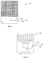
- FIG. 1A illustrates an example UICC disclosed herein.
- FIG. 1B is a side view of the example UICC of FIG. 1A .
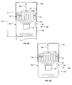
- FIG. 2A illustrates the example UICC of FIG. 1A and FIG. 1B being inserted in a first example input device in a first orientation.
- FIG. 2B illustrates the example UICC of FIG. 1A and FIG. 1B being inserted in a second example input device in the first orientation.
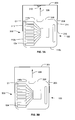
- FIG. 3A illustrates the example UICC of FIG. 1A and FIG. 1B being inserted in a third example input device in a second orientation.
- FIG. 3B illustrates the example UICC of FIG. 1A and FIG. 1B being inserted in a fourth example input device in the second orientation.
- FIG. 4A is another example UICC disclosed herein.
- FIG. 4B is a side view of the example UICC of FIG. 4A .
- FIG. 5 is another example UICC disclosed herein.
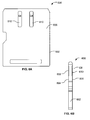
- FIG. 6A illustrates another example UICC disclosed herein.
- FIG. 6B is a side view of the example UICC of FIG. 6A .
- FIG. 7 illustrates another example UICC disclosed herein.
- FIG. 8 illustrates another example UICC disclosed herein.
- FIG. 9A is a perspective view of another example UICC disclosed herein.
- FIG. 9B is a plan view of the example UICC of FIG. 9A .
- FIG. 9C is an exploded view of the example UICC of FIG. 9A and FIG. 9B .
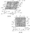
- FIG. 10A is a perspective view of another example UICC disclosed herein.
- FIG. 10B is a plan view of the example UICC of FIG. 10A .
- FIG. 11 illustrates another example UICC disclosed herein.
- FIG. 12 illustrates another example UICC disclosed herein.
- Universal integrated circuit cards are often used as a Subscriber Identity Module (e.g., SIM card, USIM card, RUIM card or CSIM card) in a portable electronic device such as a mobile device.
- a Subscriber Identity Module is a network access application that is stored in the UICC to authenticate a subscriber to a network.
- a UICC enables contactless communication (Near Field Communication) with a host (e.g., a remote terminal) based on proximity of the UICC relative to the host.
- a UICC typically includes a body to support an integrated circuit or microprocessor and a plurality of electrical contacts to enable communication between the microprocessor and a host (e.g., a computer, a mobile device, a non-mobile device, a remote terminal, etc.).
- the host typically employs an input device (e.g., a card reader) to accept the body and complete a circuit with the electrical contacts to enable communication (e.g., transfer data) between the UICC and the host.
- UICCs are governed by certain international standards provided by, for example, the European Telecommunications Standards Institute (ETSI) and the International Standard Organization (ISO).
- ETSI European Telecommunications Standards Institute
- ISO International Standard Organization
- form factor standards e.g., ID-1, plug-in UICC, a mini-UICC
- ISO/IEC 7816-2 and/or ETSI TS 102 221 standards define an overall dimensional envelope of conforming UICCs.
- mini-UICC form factor standards define an overall dimensional envelope of a UICC as 15 millimeters by 12 millimeters, which provides a surface area of 180 millimeters squared.
- the current standards define a layout of electrical contacts on the UICC as a grid pattern (e.g., 4 by 2 grid pattern) that provides a surface area greater than 1 centimeter squared.
- an order or arrangement in which electrical contacts are to be positioned on the UICC is also defined by the standards.
- the standards specify that a first row of electrical contacts should include a voltage supply, a reset, a clock and an optional first auxiliary, and a second row of electrical contacts should include a ground, a single-wire protocol, an input/output and an optional second auxiliary.
- the first row of electrical contacts typically pass across electrical contacts of an input device associated with the second row of electrical contacts when the UICC is inserted into the input device, which may cause the circuit card to become electrically damaged (e.g., short circuit).
- the supply voltage e.g., the first contact in the first row
- the ground e.g., the first contact in the second row
- an input device or card reader covers the greatest amount of surface area of an electronic board of an electronic device (e.g., a mobile phone) compared to other electronic components of the electronic device. For example, by specifying the electrical contacts or pads disposed across an (x) by (y) surface area, an input device having a minimum surface area specified by the (x) by (y) surface area of the electrical contacts is required to properly couple to the electrical contacts of the circuit card.
- smaller electronic devices are generally desirable for portability. As a result, current standards may not be sufficient to reduce the size and/or an overall footprint of a mobile device.
- Some known input devices often employ a push-push mechanism to insert/remove a UICC from an input device.
- a push-push mechanism requires a user to slide the card inside a slot of the input device. To remove the card, a user pushes the card further into the slot and a spring-loaded mechanism ejects the card from the slot.
- push-push card readers often require a door or other holding element to prevent the UICC from sliding out of the card reader (e.g., prevent unintended removal of the card).
- the door and/or holding element may damage easily and/or are relatively more expensive to manufacture.
- Another example input device or card reader employs a push-pull configuration.
- a UICC is pulled from a slot of the card reader.
- UICCs typically have relatively flat and/or smooth surfaces that make it difficult for the user to grip and pull the card from the card reader.
- some example electronic devices employ a tray-style input device or card reader.
- tray-style card-readers typically increase the overall costs and dimensional envelope of an electronic device and/or require a unique tool (e.g., a pin) to remove the tray-style card reader from an electronic device.
- example UICCs disclosed herein modify or deviate from the standards provided by ISO/IEC 7816-2 and 7816-3 and/or ETSI TS 102 221 to define another UICC form factor standard.
- UICCs disclosed herein provide significantly smaller overall footprints compared to UICCs manufactured per the current specifications and/or standards provided by ISO/IEC 7816-2 and 7816-3 and/or ETSI TS 102 221.
- the UICCs disclosed herein also reduce the overall space requirements of an input device or card reader coupled to an electronic device.
- the overall dimensional envelope of the UICC disclosed herein may have a height of between about 10.9 and 11.1 millimeters and a width of between approximately 8.9 and 9.1 millimeters.
- a UICC disclosed herein may have a surface area of approximately 99 millimeters squared, thereby significantly reducing the overall dimensional footprint or size of a UICC compared to known UICCs.
- a layout scheme of electrical contacts or electrical pads may differ from a layout provided by, for example, the current ISO/IEC 7816-2 and 7816-3 and/or the ETSI TS 102 221 standards.
- the electrical contacts disclosed herein may be disposed or coupled to the UICC in a single-row orientation or configuration.
- an electronic device may employ a header-style input device or card reader, which uses significantly less surface area of a circuit board (e.g., a logic board) of the electronic device compared to, for example, a multi-dimensional input device (e.g., a multi-row card reader).
- a supply voltage contact and a ground contact of the UICC disclosed herein can be spaced apart from each other to significantly reduce electrical damage (e.g., short circuit) and/or EMI.
- example UICCs disclosed herein may employ a locking mechanism to retain the circuit card in the input device without the use of doors.
- the locking feature also substantially prevents improper orientation of the circuit card relative to the input device and substantially prevents movement of the circuit card relative to the input device when an electronic device experiences sudden shock or vibration (e.g., if the electronic device is dropped).
- example UICCs disclosed herein may employ a lead-in feature (e.g., a chamfer).
- a pick-out feature e.g., a ridge, an opening, etc.
- FIG. 1A illustrates an example UICC 100 disclosed herein (hereinafter referred to as "UICC").
- FIG. 1B is a side view of the example UICC 100 of FIG. 1A .
- the UICC 100 comprises a body 102 defining a first or front side 104 and a second or rear side 106 opposite the first side 104.
- the first and second sides 104 and 106 of the illustrated example are spaced apart by a thickness 108 ( FIG. 1B ).
- the thickness 108 is between approximately 0.69 and 0.81 millimeters.
- a height 110 of the body 102 may be between approximately 10.9 millimeters and 11.1 millimeters and a width 112 of the body 102 may be between approximately 8.9 millimeters and 9.1 millimeters.
- the height 110 of the body 102 is approximately 11 millimeters and the width 112 of the body 102 is approximately 9 millimeters.
- the body 102 of the illustrated example includes a generally rectangular shape defining a first surface 114. More specifically, the first surface 114 has a surface area of approximately 99 millimeters squared. As shown in the illustrated example of FIG. 1A , the first surface 114 of the body 102 is defined by peripheral edges 116. In particular, the first surface 114 is defined by a first edge 118a (e.g., a left edge), a second edge 118b (e.g., an upper edge), a third edge 118c (e.g., a right edge), and a fourth edge 118d (e.g., a bottom edge).
- a first edge 118a e.g., a left edge
- a second edge 118b e.g., an upper edge
- a third edge 118c e.g., a right edge
- a fourth edge 118d e.g., a bottom edge
- the second edge 118b is positioned opposite the fourth edge 118d relative to the body 102 and the first edge 118a is positioned opposite the third edge 118c relative to the body 102.
- the second and fourth edges 118b and 118d are disposed between the first and third edges 118a and 118c, and the second and fourth edges 118b and 118d are substantially perpendicular to the first and third edges 118a and 118c.
- the first and third edges 118a and 118c are substantially parallel relative to each other and the second and fourth edges 118b and 118d are substantially parallel relative to each other.
- each of the peripheral edges 116 may include a lead-in feature 120.
- the lead-in feature 120 includes rounded corners each having a radius R1.
- the radius R1 of the illustrated example may be less than or equal to 0.80 millimeters.
- the UICC 100 includes an integrated circuit 122 (e.g., an IC).
- the UICC 100 may include a microprocessor to communicate with a host via, for example, an input device or terminal.
- the UICC of the illustrated example includes a plurality of electrical contacts or contact areas 124.
- the electrical contacts 124 are disposed on the first surface 114 adjacent the second edge 118b and between the first and third edges 118a and 118c. More specifically, in this example, the electrical contacts 124 are substantially aligned relative to each other in a single row orientation or configuration 126.
- an electronic device may employ an input device such as, for example, a header-style card reader having a significantly smaller dimensional envelope to significantly reduce an overall dimensional footprint of the electronic device.
- providing the electrical contacts 124 in the single row orientation 126 prevents the electrical contacts 124 from passing over other electrical connectors of an input device as the UICC 100 is inserted into the input device, which significantly prevents electrical damage to the UICC 100.
- the plurality of electrical contacts 124 may be disposed on the first surface 114 in a staggered pattern, an offset pattern, and/or any other suitable pattern(s).
- example UICC apparatus disclosed herein may include multiple rows of electrical contacts 124.
- the electrical contacts 124 may be disposed about a perimeter of the UICC 100 relative to the peripheral edges 116 in, for example, a square pattern, a rectangular pattern, etc.
- a classification of the electrical contacts 124 are in accordance with the classification of electrical contacts provided by standards ISO/IEC 7816-2 and 7816-3 and/or ETSI TS 102 221.
- the electrical contacts 124 of the illustrated example include a supply voltage contact C1, a reset contact C2, a clock contact C3, a first auxiliary contact C4, a ground contact C5, a single-wire protocol contact C6 (e.g., (SWP) for Near-Field Communication (NFC) or proximity transactions), an input/output contact C7, and a second auxiliary contact C8.
- the electrical contacts C4 and C8 can implement a high speed USB interface between the UICC and the host or terminal.
- the single-wire protocol contact C6 and/or the first and second auxiliary contacts C4 and C8 are optional and may be omitted.
- the UICC 100 may employ any other type of electrical contacts other than those described or represented by electrical contacts C1-C8.
- the plurality of contacts 124 are electrically coupled to the integrated circuit 122 via a plurality of wires, traces and/or a bus 128.
- the integrated circuit 122 may provide a central processor unit (CPU), volatile memory (RAM), non-volatile memory (ROM), etc.
- the supply voltage contact C1 supplies the integrated circuit 122 with electricity
- the ground contact C5 grounds the integrated circuit 122
- the reset contact C2 resets the integrated circuit 122
- the clock contact C3 provides a clock signal or time reference
- the input/output contact C7 enables performance of data input and output.
- the optional single-wire protocol contact C6 enables contactless or wireless communication with a remote terminal or host in proximity with the UICC 100.
- the optional auxiliary contacts C4 and C8 enable the UICC 100 to be coupled to, for example, Universal Serial Bus (USB) interfaces.
- USB Universal Serial Bus
- the electrical contacts 124 are arranged on the first surface 114 in a certain order to significantly reduce EMI.
- the ground contact C5 is spaced apart from the supply voltage contact C1.
- at least one other electrical contact C2-C4 and/or C6-C8 (or other electrical contacts) is disposed between the ground contact C5 and the supply voltage contact C1.
- the ground contact C5 is disposed adjacent the first edge 118a and the supply voltage contact C1 is disposed adjacent the third edge 118c.
- the ground contact C5 is spaced from the supply voltage contact C1 by a maximum distance. Further, the clock contact C3, which has the highest frequency, is disposed adjacent the ground contact C5. In this manner, separating the supply voltage contact C1 and the ground contact C5 and/or positioning the clock contact C3 adjacent the ground contact C5 significantly reduces EMI.
- the second auxiliary contact C8 is positioned adjacent the clock contact C3, the input/output contact C7 is positioned adjacent the second auxiliary contact C8, the single wire protocol contact C6 is positioned adjacent the second auxiliary contact C8, the first auxiliary contact C4 is positioned adjacent the single-wire protocol contact C6, and the reset contact C2 is positioned adjacent the first auxiliary contact C4.
- the positions of each of the electrical contacts C1-C8 comply and/or are within the specification or standards provided by ISO/IEC 7816-2 and 7816-3 and/or the ETSI TS 102 221. For example, the following table illustrates the distance of the respective electronic contacts relative to the first edge 118a as shown in FIG. 1A .
- the ground contact C5 is positioned at a distance D1 of approximately 0.3 millimeters from the first edge 118a
- the clock contact C3 is positioned at a distance D2 of approximately 1.4 millimeters from first edge 118a
- the second auxiliary contact C8 is positioned at a distance D3 of approximately 2.5 millimeters from the first edge 118a
- the single-wire protocol contact C6 is positioned at a distance D4 of approximately 3.6 millimeters from the first edge 118a
- the input/output contact C7 is positioned at a distance D5 of approximately 4.7 millimeters from the first edge 118a
- the first auxiliary contact C4 is positioned at a distance D6 of approximately 5.8 millimeters from the first edge 118a
- the reset contact C2 is positioned at a distance D7 of approximately 6.9 millimeters from the first edge 118a
- the supply voltage contact C1 is positioned at a distance D8 of approximately 8.0 millimeters from the first edge 118
- Each of the electrical contacts 124 of the illustrated example has a rectangular shape. As shown in FIG. 1A , each of the electrical contacts 124 has a width W1 and a height H1. In this example, the width W1 is approximately 0.7 millimeters and the height H1 is approximately 3.0 millimeters. However, in other examples, each of the electrical contacts 124 may have a different sized height H1, width W1 and/or may have a square shape, rounded corners and/or any other suitable shape or configuration or any combination thereof. In addition, the electrical contacts 124 are equally spaced apart by a distance W2. In the illustrated example, the distance W2 is approximately 0.40 millimeters. Further, both the ground contact C5 and the supply voltage contact C1 are spaced from the respective first and third edges 118a and 118c by a distance of approximately 0.3 millimeters.
- the electrical contacts 124 illustrated in FIG. 1A can be disposed in any order.
- the electrical contacts 124 may be disposed sequentially C1-C8 and/or in any other suitable order.
- the first auxiliary input C4 may be disposed adjacent the first edge 118a of the body 102 instead of the ground contact C5 and/or the second auxiliary input C8 may be disposed adjacent the third edge 118c.
- the overall width 112 of the UICC 100 can be further reduced in examples in which the auxiliary contacts C4 and C8 are omitted.
- the electrical contacts 124 may include different contacts other than the electrical contacts associated with the classifications C1-C8 as described in FIG. 1A . Further, in some examples, any one of the electrical contacts C1-C8 may be omitted or replaced with another electrical contact.
- the example UICC 100 includes a buffer area 130 between the second edge 118b and an upper edge 132 of each of the electrical contacts 124.
- the electrical contacts 124 are offset relative to the second edge 118b by an offset distance V1.
- the offset distance V1 may be between approximately 0.1 millimeters and 0.50 millimeters.
- the rounded corners of the body 102 help maintain a substantially consistent or relatively even buffer area 130 adjacent the corners of the body 102.
- the UICC 100 of the illustrated example employs a grip or pick-out feature 134.
- the pick-out feature 134 is disposed adjacent the fourth edge 118d between the first and third edges 118a and 118c.
- the pick-out feature 134 is a slot or opening.
- the slot shown in FIG. 1A is defined by a rectangular portion 136 disposed between first and second arcuate or circular ends 136a and 136b.
- a first portion of the rectangular portion is positioned at a distance V4 relative to the second edge 118b and a second portion of the rectangular portion 136 is positioned at a distance V5 from the second edge 118b.
- the distance V4 may be between approximately 9.69 and 9.71 millimeters and the distance V5 may be between approximately 10.39 and 10.41 millimeters such that the slot defines an opening sized between approximately 0.68 and 0.72 millimeters.
- the pick-out feature 134 may be omitted.
- a first center 138a of the first arcuate end 136a is positioned at a distance P1 from the first edge 118a and a second center 138b of the second arcuate end 136b is positioned at a distance P2 from the first edge 118a.
- the first distance P1 is between approximately 1.9 and 2.1 millimeters and the second distance P2 is between approximately 6.9 and 7.1 millimeters from the first edge 118a.
- the pick-out feature 134 may be a slot having an opening that is recessed in the first surface 114. In other words, a slot forms a recessed opening that does not pass through the entire thickness 108 of the body 102.
- the pick-out feature 134 may be a raised lip portion, an aperture and/or any other surface or feature to enable or facilitate handling the UICC 100.
- the example UICC 100 includes a notch or locking feature 140. More specifically, the notch 140 retains the UICC 100 within an input device and prevents the UICC from moving (e.g., bouncing) or dislodging from the input device when, for example, the electronic device experiences a sudden shock (e.g., the device is dropped). Additionally or alternatively, the notch 140 significantly reduces or prevents misalignment and facilitates proper orientation of the UICC 100 relative to the input device when the UICC 100 is coupled to the input device as described in greater detail below in connection with FIG. 3A .
- the notch 140 of the illustrated example is disposed along the third edge 118c of the body 102.
- the notch 140 forms a recessed edge 142 spaced away from the third edge 118c and toward the first edge 118a.
- the recessed edge 142 is positioned at a distance of P3 relative to the first edge 118a.
- the distance P3 is between approximately 8.29 and 8.31 millimeters.
- the notch 140 of the illustrated example forms a recessed opening 144 having a shoulder or catch feature 146 between a first portion 148a of the third edge 118c and a first end 142a of the recessed edge 142 and a substantially tapered edge 150 between a second portion 148b of the third edge 118c and a second end 142b of the recessed edge 142.
- the shoulder 146 is substantially parallel relative to the second edge 118b and substantially perpendicular relative to the first portion 148a of the third edge 118c.
- the shoulder 146 is positioned at a distance V2 from the second edge 118b of the body 102.
- the distance V2 is between approximately 4.49 and 4.51 millimeters.
- the tapered edge 150 intersects the second portion 148b of the third edge 118c at a position V3 relative to the second edge 118b of the body 102.
- the distance V3 is between approximately 6.68 and 6.7 millimeters.
- the example body 102 includes a radius R2 between the shoulder 146 and the recessed edge 142 and a radius R3 between the tapered edge 150 and the recessed edge 142.
- the radius R2 is less than or equal to 0.3 millimeters and the radius R3 is less than or equal to 0.7 millimeters.
- the notch 140 may be omitted.
- the notch 140 may have any other shape or profile such as described in FIGS. 11 and 12 .
- the example UICC 100 of FIGS. 1A and 1B may be formed via, for example, a punch-out flat sheet manufacturing process(es).
- the body 102 may be composed of, for example, a plastic material and the pick-out feature 134 and/or the notch 140 are formed via, for example, a punching process(es).
- the electrical contacts 124 may comprise a unitary sheet composed of electrically conductive material (e.g., copper, etc.) having divided contacts C1-C8 that may be coupled to the first surface 114 of the body 102 via, for example, glue, solder, or any other suitable fastener(s).
- the integrated circuit 122 may be positioned or coupled to the body via, for example, a pick and place robot or other manufacturing equipment. For example, the integrated circuit may be soldered onto the first surface 114 of the body 102.
- the wires or traces 128 may be coupled to the body 102 via wire bonding manufacturing techniques or process(es).
- the body 102 of the example UICC 100 may be composed of a plastic material formed via, for example, injection molding.
- the body 102 and/or the UICC 100 can be manufactured with more precise tolerances (e.g., relatively tighter tolerances) compared to the flat sheet manufacturing process as described above.
- the UICC 100 can be manufactured such that the dimensions D1-D8, P1-P3, V1-V5, R1-R3, H1, W1, W2, the height 110 and/or the width 112 can be within a tolerance value of approximately 0.1 millimeters.
- FIG. 2A illustrates the example UICC 100 of FIGS. 1A and 1B being inserted in an example input device or card reader 200 in a first orientation 202.
- the input device 200 enables communication between the UICC 100 and a host such as, for example, a computer, a point of sale terminal, a remote terminal, a mobile device, etc.
- the input device 200 provides power to the UICC 100 or the integrated circuit 122 and also performs protocol conversation and/or reformats data for use by the UICC 100.
- the UICC 100 is inserted in an opening or cavity 204 of the input device 200 with a leading edge 206 (e.g., the second edge 118b) of the body 102 oriented in a direction represented by arrow 208.
- a leading edge 206 e.g., the second edge 118b
- the electrical contacts 124 do not pass over or across other electrical contacts or connectors of the input device 200 when the UICC 100 is inserted in the opening 204.
- the supply voltage contact C1 is adjacent the third edge 118c and electrically couples to the input device 200 only when the UICC 100 is fully inserted in the opening 204.
- the electrical contacts 124 simultaneously engage their respective electrical contacts (e.g., not shown) of the input device 200 when the UICC 100 is inserted in the input device 200.
- the UICC 100 receives power only after the UICC 100 is fully inserted and properly oriented relative to the opening 204 of the input device 200.
- Such a configuration prevents electrical damage to the electrical contacts 124, the UICC 100 and/or the input device 200.
- placement of the clock electrical contact C3, which has the highest frequency, adjacent the ground electrical contact C5 significantly reduces EMI.
- the notch 140 can engage a lock or catch feature 210 of the input device 200 to secure the UICC 100 in the opening 204 of the input device 200.
- the UICC 100 remains secured within the input device 200.
- the UICC 100 is moved in the direction of arrow 208 when the UICC 100 is in the opening 204 such that the tapered surface 150 releases the lock or catch feature 210 from the shoulder 142 of the notch 140 (e.g., the tapered surface 150 biases the catch feature 210 away from the notch 140).
- a spring-loaded ejection mechanism (not shown) can then eject the UICC 100 from the opening 204 and the pick-out feature 134 enables a user to firmly grasp the UICC 100 and pull it away from the opening 204 in a direction opposite of the direction indicated by the arrow 208.
- providing the height 110 with a dimensional value that is different than the dimensional value of the width 112 significantly prevents erroneous insertion into the opening 204 of the input device 200.
- FIG. 2B illustrates the example UICC 100 of FIGS. 1A and 1B being inserted in another example input device or card reader 201 in the first orientation 202.
- the example input device 201 of FIG. 2B does not include the locking feature 210 as shown in FIG. 2A . Nonetheless, the UICC 100 properly fits within an opening 205 of the input device 201.
- FIG. 3A illustrates the example UICC 100 of FIGS. 1A and 1B being inserted in another example input device or card reader 300 in a second orientation 302.
- the UICC 100 shown in FIG. 3A is inserted in an opening 304 of the input device 300 with the third edge 118c of the body 102 as a leading edge 306 oriented in a direction represented by arrow 308.
- the orientation of the electrical contacts 124 as shown in FIGS. 1A and 1B prevent electrical damage when the UICC 100 is inserted into the input device 300.
- the supply voltage contact C1 is adjacent the third edge 118c or the leading edge 306, the supply voltage contact C1 is the last electrical contact 124 to couple to a respective electrical contact or connector (not shown) of the input device 300 and does not drag the other electrical contacts 124 across power.
- the UICC 100 is not powered during insertion of the UICC 100 into the input device 300, thereby significantly reducing potential short circuits and/or electrical damage to the UICC 100.
- the UICC 100 receives power only after the UICC 100 is fully inserted into the opening 204 of the input device 300.
- the notch 140 as shown in FIG. 3A facilitates or enables proper orientation of the UICC 100 relative to the opening 304 of the input device 300. More specifically, when the UICC 100 is properly oriented relative the input device 300, a guide feature 310 (e.g., a protrusion) of the input device 300 nests within the recessed opening 144 formed or defined by the notch 140. In this manner, the UICC 100 can only be properly inserted within the opening 304 of the input device 300 when the leading edge 306 of the UICC 100 is inserted within the opening 304 and the second edge 118b of the UICC 100 is adjacent a first side 312 of the input device 300.
- a guide feature 310 e.g., a protrusion
- the UICC 100 may not properly fit within the opening 304 if the second edge 118b is adjacent a second side 314 of the input device 300 even if the leading edge 306 is properly oriented relative to the opening 304 due to interference between the guide feature 310 and the edge 118c adjacent the notch 140.
- the guide feature 310 interferes with the first edge 118a to prevent the UICC 300 from properly fitting within the opening 304.
- the UICC 100 properly fits within the opening 304 when the first edge 118a of the UICC 100 substantially aligns with an end 316 of the opening 304 and/or the input device 300.
- improper orientation may cause the first edge 118a of the UICC 100 to project away from the opening 304 relative to the end 316.
- FIG. 3B illustrates the example UICC 100 of FIGS. 1A and 1B being inserted in another example input device or card reader 301 in the second orientation 302.
- the example input device 301 of FIG. 3B does not include the guide feature 310 shown in FIG. 3A . Nonetheless, the UICC 100 properly fits within an opening 303 of the input device 301.
- FIG. 4A is a plan view of another example UICC 400 disclosed herein.
- the example UICC 400 of FIG. 4A includes a body 402 defining a first side or surface 404 and a second surface or surface 406 opposite the first surface 404.
- the first and second surfaces 404 and 406 of the illustrated example are spaced apart to define a body thickness 408.
- the example UICC 400 of FIG. 4A employs a lead-in feature 410.
- the lead-in feature 410 is disposed on a leading end 412 of the UICC 400.
- each of the first and second surfaces 404 and 406 includes the lead-in feature 410.
- the lead-in feature 410 of the illustrated example includes tapered edges 414a and 414b adjacent the leading edge 412.
- the lead-in feature 410 may be chamfered edges, angled edges, rounded edges, or any other shaped-edge to facilitate insertion of the UICC 400 in an input device such as the input device 200 of FIG. 2 .
- the lead-in feature 410 may be formed via secondary manufacturing process(es) such as, for example, machining (e.g., chamfer milling) and/or other suitable manufacturing process(es).
- the lead-in feature 410 may be formed via injection molding to eliminate a secondary manufacturing process as described in greater detail below in connection with FIG. 9A, FIG. 9B and FIG. 9C .
- FIG. 5 illustrates another example UICC 500 disclosed herein.
- the UICC 500 of FIG. 5 is implemented with a plurality of electrical contacts 502 (e.g., six electrical contacts).
- the electrical contacts 502 may include, for example, the ground contact C5, the clock contact C3, the single-wire protocol contact C6, the input/output contact C7, the reset contact C2 and the supply voltage contact C1.
- the first and second auxiliary electrical contacts C4 and C8 of FIGS. 1A and 1B may be omitted.
- the UICC 500 may include only one of the auxiliary electrical contacts C4 or C8 of FIG. 1A .
- FIG. 6A illustrates another example UICC 600 disclosed herein.
- FIG. 6B is a side view of another example UICC 600 disclosed herein.
- the UICC 600 of FIG. 6A and FIG. 6B is a dual-sided UICC.
- the UICC 600 of FIG. 6A includes a body 602 defining a first side or surface 604 ( FIG. 6B ) and a second side or surface 606 opposite the first surface 604.
- the first surface 604 of the UICC 600 includes one or more electrical contacts 608 and the second surface 606 of the UICC 600 includes one or more electrical contacts 610.
- the electrical contacts 608 disposed on the first surface 604 of the UICC 600 may include the electrical contacts C1-C3, C5-C7 as shown, for example, in FIG. 5
- the electrical contacts 610 disposed on the second surface 606 may include, for example, the first and second auxiliary contacts C4 and C8 of FIG. 1A
- a dual-sided header-style input device or card reader may be employed to communicatively couple the electrical contacts on both surfaces 604 and 606 of the UICC 600 to a host (e.g., an electrical device).
- FIG. 7 illustrates another example UICC 700 disclosed herein.
- the UICC 700 includes a body 702 defining a first side or surface 704 that includes a plurality of electrical contacts 706.
- an electrical contact 708 of the plurality of electrical contacts 706 has a different size and/or shape than the other ones of the electrical contacts 710. More specifically, the electrical contact 708 expands or covers a greater surface area 712 of the first surface 704 relative to the other electrical contacts 710.
- the electrical contact 708 may be a ground electrical contact C5. Increasing a surface area of the ground electrical contact C5 may significantly reduce EMI.
- FIG. 8 illustrates another example UICC 800 disclosed herein. More specifically, the UICC 800 of FIG. 8 illustrates another example electrical contact configuration 802 expanding across a surface area 804 of a first side or surface 806 of a body 808 of the UICC 800.
- the UICC 800 includes a first plurality of electrical contacts 810 and a second plurality of electrical contacts 812.
- the first plurality of electrical contacts 810 are interconnected or electrically coupled via a coupling portion 814 to cover a greater amount of the surface area 804 of the first surface 806 than for example the electrical contacts 810 or the electrical contacts 124 of FIG. 1A .
- the first plurality of electrical contacts 810 and the coupling portion 814 may be the ground electrical contact C5.
- an electrical contact and/or the coupling portion 814 may span across substantially the entire surface area 804 of the first surface 806 between peripheral edges 816a-d of the UICC 800.
- FIG. 9A illustrates a perspective view of another example UICC 900 disclosed herein.
- FIG. 9B is a plan view of the example UICC 900 of FIG. 9B.
- FIG. 9C is an exploded view of the example UICC 900 of FIGS. 9B and 9C .
- the UICC 900 of FIGS. 9A-9C includes a body 902 defining a first side or surface 904 and a second side or surface 906 opposite the first surface 904.
- the body 902 or the first surface 904 is approximately 9 millimeters by 11 millimeters and defines a surface area 904a of approximately 99 millimeters squared.
- the body 902 of the illustrated example is composed of a plastic material (e.g., a Laser Direct Structuring (LDS) resin) and is formed via, for example, injection molding.
- LDS Laser Direct Structuring
- the example body 902 may include a recessed cavity 912 to receive an integrated circuit or microprocessor 914.
- forming the body 902 via, for example, injection molding enables the body 902 to be formed with relatively more precise and/or tighter tolerances compared to other manufacturing process(es) such as, the flat sheet manufacturing process(es) described above.
- forming the body 902 via injection molding provides a relatively smoother surface finish to the first surface 904 and/or the second surface 906 and provides relatively smoother corners 908a-d or edges 910a-d compared to other manufacturing process(es) such as the flat-sheet manufacturing process.
- Providing relatively smoother surface finishes, corners and/or edges facilitates insertion and/or an interaction between the UICC 900 and an input device or card reader.
- one or more electrical contacts 916 and/or one or more electrical traces or connectors 918 electrically coupling the electrical contacts 916 to the integrated circuit 914 may be formed or etched in the body 902 via, for example, LDS manufacturing process.
- LDS manufacturing process enables injection molded plastic parts to be selectively plated with discrete circuit pathways (i.e., the traces 918).
- a laser basically etches, writes or prints a conductive pattern corresponding to the position of the electrical contacts 916 and/or the electrical connectors 918 onto the first surface 904 of the body 902 after the body 902 is formed via injection molding.
- the body 902 is then immersed within a copper bath to provide the conductive electrical contacts 916 and/or traces 918.
- the electrical contacts 916 may include the electrical contacts C1-C8 described in FIG. 1A and may include the electrical contact orientation or layout provided by the example UICC 100 of FIG. 1A .
- the integrated circuit or microprocessor 914 may then be disposed in the cavity 912 of the body 902 via, for example, a pick and place robot and the integrated circuit or microprocessor 914 may be coupled to the body 902 via, for example, soldering.
- a cover or screen 920 such as a laminate cover may be coupled to the body 902 and disposed over the integrated circuit 914 to protect the integrated circuit from debris and/or other contaminates.
- the example UICC 900 of the illustrated example includes a lead-in feature 922 adjacent a leading edge 924.
- the lead-in feature 922 may be the rounded corners 908b and 908c and/or may include an arcuate or curved shaped profile.
- the lead-in feature 922 may be a tapered or chamfered edge adjacent the leading edge 924 such as, for example, the tapered or chamfered edge 410 illustrated in FIG. 4A .
- the lead-in feature 922 may be formed during the injection molding process.
- the example lead-in feature 922 may be formed with the body 902, thereby eliminating secondary manufacturing process(es) and/or significantly reducing costs.
- the example UICC of FIGS. 9A-9C also includes a pick-out feature 926 to facilitate removal of the UICC 900 from an input device.
- the pick-out feature 926 comprises a raised lip or molded ridge 928 protruding away from the first surface 904 adjacent the edge 910d of the first surface 904.
- the raised lip 928 has an arcuate profile, edge or shape.
- the second surface 906 opposite the first surface 904 may also include a raised lip or molded ridge (e.g., similar to the raised lip 928) protruding away from the second surface 906.
- the raised lip or molded ridge 928 may be disposed on the second surface 906 instead of the first surface 904.
- the body 902 of the illustrated example also includes a notch 930.
- the notch 930 is formed on the edge 910c of the body 902 between the electrical contacts 916 and the raised lip 928 and provides a catch or locking feature similar to the locking feature described in connection with FIGS. 1A and 1B .
- FIG. 10A is a perspective view of another example UICC 1000 disclosed herein.
- FIG. 10B is a plan view of the example UICC 1000 of FIG. 10A .
- the UICC 1000 comprises a body 1002 defining a first or front surface or side 1004 and a second or rear surface or side 1006 opposite the first surface 1004.
- the body 1002 of the illustrated example includes a plurality of electrical contacts 1008 positioned or arranged in a plurality of rows 1008a and 1008b.
- a first row 1008a of electrical contacts 1008 may include the supply voltage contact C1 adjacent a first edge 1010, the reset contact C2 adjacent the supply voltage contact C1, the clock contact C3 adjacent the reset contact C2, and the first auxiliary contact C4 adjacent the clock contact C3 and/or a second edge 1012.
- a second row 1008b of electrical contacts 1008 may include the ground contact C5 adjacent the first edge 1010 and below the supply voltage contact C1, the single-wire protocol contact C6 adjacent the ground contact C5, the input/output contact C7 adjacent the single-wire protocol contact C6, and the second auxiliary contact C8 adjacent the input/output contact C7.
- the supply voltage contact C1 and the ground contact C5 may be disposed a distance of approximately 0.45 millimeters from the first edge 1010
- the reset contact C2 and the single-wire protocol electrical contact C6 may be disposed a distance of approximately 2.65 millimeters from the first edge 1010
- the clock contact C3 and the input/output contact C7 may be disposed a distance of approximately 4.85 millimeters from the first edge 1010
- the first and second auxiliary contacts C4 and C8 may be positioned at a distance of approximately 7.05 millimeters from the first edge 1010.
- first row 1008a of electrical contacts 1008 may be positioned at a distance of approximately 0.5 millimeters from a third edge 1014 and the second row 1008b of electrical contacts 1008 may be positioned at a distance of approximately 5.80 millimeters from the third edge 1014.
- a spacing or area S1 between each of the electrical contacts 1008 may be, for example, 0.75 millimeters.
- the supply voltage contact C1 and the ground contact C5 may be positioned from the first edge 1010 at a distance of approximately 0.45 millimeters and the each of the first and second auxiliary contacts C4 and C8 may be positioned from the second edge 1012 at a distance of approximately 0.45 millimeters.
- Each of the electrical contacts 1008 of the illustrated example has a substantially square shape or profile. As shown in FIG. 10B , a width W1 of each of the electrical contacts 1008 is approximately 1.5 millimeters and a height H1 of each of the electrical contacts 1008 is approximately 1.5 millimeters. However, in other examples, each of the electrical contacts 1008 may have a rectangular shape and/or any other suitable shape or configuration and/or a combination thereof.
- Each of the electrical contacts 1008 is electrically coupled to an integrated circuit or microprocessor 1018 via respective traces or wires 1020.
- the electrical contacts 1008 may be coupled to the body 1002 (e.g., via a glue, solder, etc.) and the traces or wires 1020 may be coupled to the body 1002 via, for example, wire bonding manufacturing process.
- the body 1002 may be formed via injection molding and the electrical contacts 1008 and/or the traces or wires 1020 may be formed on the body 1002 via, for example, LDS manufacturing process.
- the example UICC 1000 of the illustrated example also includes a pick-out feature 1022.
- the pick-out feature 1022 is an aperture or hole 1024 disposed adjacent a fourth edge 1026.
- the aperture 1024 is formed adjacent a corner 1028 defined by the first edge 1010 and the fourth edge 1026.
- the pick-out feature 1022 may be disposed between the first and third edges 1010 and 1014 or adjacent a corner formed by the third 1014 and a fourth edge 1026.
- the example UICC 1000 of the illustrated example also employs a notch 1030 to secure the UICC 100 in a card reader.
- the notch 1030 is formed along the third edge 1014 between the second row of electrical contacts 1008b and the fourth edge 1026. Because the UICC 1000 includes the first and second rows 1008a and 1008b of electrical contacts 1008 disposed over a greater amount of surface area of the first surface 1004 of the body 1002, the notch 1030 is formed adjacent the fourth edge 1026.
- the notch 1030 includes a shoulder 1032 to provide a stop or engage a catch feature of an input device and a tapered surface 1034 to release the catch feature when the UICC 1000 is removed from the input device.
- the input device may be a card reader such as a two-row, header-style card reader.
- the UICC 100 may include a cover or laminate 1036.
- the cover 1036 of the illustrated example is coupled to the first surface 1004 and disposed over the electrical contacts 1024 and the integrated circuit 1018.
- FIG. 11 illustrates another example UICC 1100 having another example locking feature or notch 1102 described herein.
- the notch 1102 has a substantially arcuate profile or shape 1104 forming a cavity 1106 to engage, accept, release and/or interact with a locking mechanism (e.g. a biasing element or spring) of an input device.
- a locking mechanism e.g. a biasing element or spring
- the arcuate profile 1104 of the illustrated example has a semi-circular or circular shape or profile 1108.
- the arcuate shape 1104 may have an oval shape, an elliptical shape, and/or may employ any other suitable shape or profile to engage a locking mechanism of, for example, an input device.
- FIG. 12 illustrates another example UICC 1200 having another example locking feature or notch 1202 described herein.
- the notch 1202 has a substantially arcuate profile or shape 1204 forming a cavity 1206 to engage, accept, release and/or interact with a locking mechanism (e.g. a biasing element or spring) of an input device.
- a locking mechanism e.g. a biasing element or spring
- the arcuate profile 1204 of the illustrated example has an oval or elliptical profile 1208.
- the arcuate shape 1204 may have a circular shape or profile and/or may employ any other suitable shape or profile to engage a locking mechanism of, for example, an input device.
Landscapes
- Engineering & Computer Science (AREA)
- Computer Hardware Design (AREA)
- Microelectronics & Electronic Packaging (AREA)
- Physics & Mathematics (AREA)
- General Physics & Mathematics (AREA)
- Theoretical Computer Science (AREA)
- Telephone Set Structure (AREA)
- Credit Cards Or The Like (AREA)
Priority Applications (2)
| Application Number | Priority Date | Filing Date | Title |
|---|---|---|---|
| CA2791674A CA2791674C (en) | 2011-11-07 | 2012-10-03 | Universal integrated circuit card apparatus and related methods |
| CN201210377697.5A CN103218649B (zh) | 2011-11-07 | 2012-10-08 | 通用集成电路卡装置及相关方法 |
Applications Claiming Priority (1)
| Application Number | Priority Date | Filing Date | Title |
|---|---|---|---|
| US13/290,874 US8649820B2 (en) | 2011-11-07 | 2011-11-07 | Universal integrated circuit card apparatus and related methods |
Publications (3)
| Publication Number | Publication Date |
|---|---|
| EP2590112A2 true EP2590112A2 (de) | 2013-05-08 |
| EP2590112A3 EP2590112A3 (de) | 2014-11-05 |
| EP2590112B1 EP2590112B1 (de) | 2019-07-10 |
Family
ID=46551357
Family Applications (1)
| Application Number | Title | Priority Date | Filing Date |
|---|---|---|---|
| EP12169339.4A Active EP2590112B1 (de) | 2011-11-07 | 2012-05-24 | Chipkarte |
Country Status (4)
| Country | Link |
|---|---|
| US (1) | US8649820B2 (de) |
| EP (1) | EP2590112B1 (de) |
| CN (1) | CN103218649B (de) |
| CA (1) | CA2791674C (de) |
Cited By (1)
| Publication number | Priority date | Publication date | Assignee | Title |
|---|---|---|---|---|
| WO2018005134A1 (en) * | 2016-06-29 | 2018-01-04 | Giesecke+Devrient Mobile Security America, Inc. | Automatic sim punch and method |
Families Citing this family (44)
| Publication number | Priority date | Publication date | Assignee | Title |
|---|---|---|---|---|
| USD707682S1 (en) * | 2012-12-05 | 2014-06-24 | Logomotion, S.R.O. | Memory card |
| USD758372S1 (en) * | 2013-03-13 | 2016-06-07 | Nagrastar Llc | Smart card interface |
| US9647997B2 (en) | 2013-03-13 | 2017-05-09 | Nagrastar, Llc | USB interface for performing transport I/O |
| US9888283B2 (en) | 2013-03-13 | 2018-02-06 | Nagrastar Llc | Systems and methods for performing transport I/O |
| USD759022S1 (en) * | 2013-03-13 | 2016-06-14 | Nagrastar Llc | Smart card interface |
| USD729808S1 (en) | 2013-03-13 | 2015-05-19 | Nagrastar Llc | Smart card interface |
| KR20160013196A (ko) * | 2013-05-29 | 2016-02-03 | 비자 인터네셔널 서비스 어소시에이션 | 보안 요소에서 수행되는 검증 시스템 및 방법 |
| USD716743S1 (en) * | 2014-03-25 | 2014-11-04 | Transcend Information, Inc. | Printed circuit board of solid-state memory |
| USD736775S1 (en) * | 2014-05-02 | 2015-08-18 | Samsung Electronics Co., Ltd. | Memory card |
| USD730907S1 (en) * | 2014-05-02 | 2015-06-02 | Samsung Electronics Co., Ltd. | Memory card |
| USD730911S1 (en) * | 2014-05-02 | 2015-06-02 | Samsung Electronics Co., Ltd. | Memory card |
| USD735725S1 (en) * | 2014-05-02 | 2015-08-04 | Samsung Electronics Co., Ltd. | Memory card |
| USD730908S1 (en) * | 2014-05-02 | 2015-06-02 | Samsung Electronics Co., Ltd. | Memory card |
| USD730910S1 (en) * | 2014-05-02 | 2015-06-02 | Samsung Electronics Co., Ltd. | Memory card |
| USD729251S1 (en) * | 2014-06-27 | 2015-05-12 | Samsung Electronics Co., Ltd. | Memory card |
| USD727911S1 (en) * | 2014-06-27 | 2015-04-28 | Samsung Electronics Co., Ltd. | Memory card |
| USD727913S1 (en) * | 2014-06-27 | 2015-04-28 | Samsung Electronics Co., Ltd. | Memory card |
| USD730909S1 (en) * | 2014-06-27 | 2015-06-02 | Samsung Electronics Co., Ltd. | Memory card |
| USD727912S1 (en) * | 2014-06-27 | 2015-04-28 | Samsung Electronics Co., Ltd. | Memory card |
| USD736214S1 (en) * | 2014-07-01 | 2015-08-11 | Samsung Electronics Co., Ltd. | Memory card |
| USD736215S1 (en) * | 2014-07-01 | 2015-08-11 | Samsung Electronics Co., Ltd. | Memory card |
| USD736212S1 (en) * | 2014-07-01 | 2015-08-11 | Samsung Electronics Co., Ltd. | Memory card |
| USD736213S1 (en) * | 2014-07-01 | 2015-08-11 | Samsung Electronics Co., Ltd. | Memory card |
| USD727910S1 (en) * | 2014-07-02 | 2015-04-28 | Samsung Electronics Co., Ltd. | Memory card |
| USD739856S1 (en) * | 2014-07-30 | 2015-09-29 | Samsung Electronics Co., Ltd. | Memory card |
| USD736216S1 (en) * | 2014-07-30 | 2015-08-11 | Samsung Electronics Co., Ltd. | Memory card |
| USD756317S1 (en) * | 2014-08-26 | 2016-05-17 | Féinics Amatech Teoranta | Layout for contact pads and connection bridges of a transponder chip module |
| CN105430120A (zh) * | 2014-09-16 | 2016-03-23 | 中兴通讯股份有限公司 | 一种手机塞子弹出系统、手机及手机塞子弹出方法 |
| USD780763S1 (en) | 2015-03-20 | 2017-03-07 | Nagrastar Llc | Smart card interface |
| USD864968S1 (en) | 2015-04-30 | 2019-10-29 | Echostar Technologies L.L.C. | Smart card interface |
| USD798868S1 (en) * | 2015-08-20 | 2017-10-03 | Isaac S. Daniel | Combined subscriber identification module and storage card |
| USD783621S1 (en) * | 2015-08-25 | 2017-04-11 | Samsung Electronics Co., Ltd. | Memory card |
| USD783622S1 (en) * | 2015-08-25 | 2017-04-11 | Samsung Electronics Co., Ltd. | Memory card |
| USD772232S1 (en) * | 2015-11-12 | 2016-11-22 | Samsung Electronics Co., Ltd. | Memory card |
| USD773467S1 (en) * | 2015-11-12 | 2016-12-06 | Samsung Electronics Co., Ltd. | Memory card |
| CN107025481B (zh) * | 2016-02-02 | 2021-08-20 | 上海伯乐电子有限公司 | 柔性印制电路板及应用其的智能卡模块和智能卡 |
| JP1564043S (de) * | 2016-04-27 | 2017-11-13 | ||
| JP1564455S (de) * | 2016-05-11 | 2017-11-13 | ||
| DE102016110780B4 (de) * | 2016-06-13 | 2024-10-10 | Infineon Technologies Austria Ag | Chipkartenmodul und Verfahren zum Herstellen eines Chipkartenmoduls |
| USD798251S1 (en) * | 2016-11-07 | 2017-09-26 | Transcend Information, Inc. | Printed circuit board of solid-state memory |
| USD875056S1 (en) * | 2017-06-08 | 2020-02-11 | Jie Qi | Flexible printed circuit board |
| FR3073307B1 (fr) * | 2017-11-08 | 2021-05-28 | Oberthur Technologies | Dispositif de securite tel qu'une carte a puce |
| KR102834549B1 (ko) * | 2020-08-14 | 2025-07-14 | 삼성전자주식회사 | 메모리 카드 |
| KR102417495B1 (ko) * | 2022-04-28 | 2022-07-05 | 지인석 | Fpcb를 활용한 커넥팅 프로브 카드 |
Family Cites Families (492)
| Publication number | Priority date | Publication date | Assignee | Title |
|---|---|---|---|---|
| US3373481A (en) | 1965-06-22 | 1968-03-19 | Sperry Rand Corp | Method of electrically interconnecting conductors |
| US3676742A (en) | 1971-05-24 | 1972-07-11 | Signetics Corp | Means including a spark gap for protecting an integrated circuit from electrical discharge |
| CA954635A (en) | 1972-06-06 | 1974-09-10 | Microsystems International Limited | Mounting leads and method of fabrication |
| US3842189A (en) | 1973-01-08 | 1974-10-15 | Rca Corp | Contact array and method of making the same |
| USD261760S (en) | 1978-12-22 | 1981-11-10 | Pitney Bowes Inc. | Electronic postal rate memory |
| DE3029667A1 (de) | 1980-08-05 | 1982-03-11 | GAO Gesellschaft für Automation und Organisation mbH, 8000 München | Traegerelement fuer einen ic-baustein |
| DE3029939A1 (de) | 1980-08-07 | 1982-03-25 | GAO Gesellschaft für Automation und Organisation mbH, 8000 München | Ausweiskarte mit ic-baustein und verfahren zu ihrer herstellung |
| US4549247A (en) | 1980-11-21 | 1985-10-22 | Gao Gesellschaft Fur Automation Und Organisation Mbh | Carrier element for IC-modules |
| FR2505091A1 (fr) | 1981-04-30 | 1982-11-05 | Cii Honeywell Bull | Dispositif de protection des circuits electroniques tels que des circuits integres a l'encontre des charges electrostatiques |
| DE3130324A1 (de) | 1981-07-31 | 1983-02-17 | GAO Gesellschaft für Automation und Organisation mbH, 8000 München | Traegerelement fuer einen ic-baustein |
| DE3151408C1 (de) | 1981-12-24 | 1983-06-01 | GAO Gesellschaft für Automation und Organisation mbH, 8000 München | Ausweiskarte mit einem IC-Baustein |
| CA1204213A (en) * | 1982-09-09 | 1986-05-06 | Masahiro Takeda | Memory card having static electricity protection |
| US4535219A (en) | 1982-10-12 | 1985-08-13 | Xerox Corporation | Interfacial blister bonding for microinterconnections |
| JPS59229686A (ja) | 1983-06-09 | 1984-12-24 | Toshiba Corp | Icカ−ド |
| EP0128822B1 (de) | 1983-06-09 | 1987-09-09 | Flonic S.A. | Verfahren zur Herstellung von Speicherkarten und hierdurch hergestellte Karten |
| DE3338597A1 (de) | 1983-10-24 | 1985-05-02 | GAO Gesellschaft für Automation und Organisation mbH, 8000 München | Datentraeger mit integriertem schaltkreis und verfahren zur herstellung desselben |
| DE3420051A1 (de) | 1984-05-29 | 1985-12-05 | GAO Gesellschaft für Automation und Organisation mbH, 8000 München | Datentraeger mit ic-baustein und verfahren zur herstellung eines derartigen datentraegers |
| FR2579798B1 (fr) | 1985-04-02 | 1990-09-28 | Ebauchesfabrik Eta Ag | Procede de fabrication de modules electroniques pour cartes a microcircuits et modules obtenus selon ce procede |
| FR2584235B1 (fr) | 1985-06-26 | 1988-04-22 | Bull Sa | Procede de montage d'un circuit integre sur un support, dispositif en resultant et son application a une carte a microcircuits electroniques |
| DE3689094T2 (de) | 1985-07-27 | 1994-03-10 | Dainippon Printing Co Ltd | IC-Karte. |
| FR2588695B1 (fr) | 1985-10-11 | 1988-07-29 | Eurotechnique Sa | Procede de fabrication d'un microboitier, microboitier a contacts effleurants et application aux cartes contenant des composants |
| US4755661A (en) | 1986-01-10 | 1988-07-05 | Ruebsam Herrn H | Connection of electronic components in a card |
| JPS62214998A (ja) | 1986-03-17 | 1987-09-21 | 三菱電機株式会社 | 薄型半導体カ−ド |
| JPH0815167B2 (ja) | 1986-03-26 | 1996-02-14 | 株式会社日立製作所 | 半導体装置 |
| DE3639630A1 (de) | 1986-11-20 | 1988-06-01 | Gao Ges Automation Org | Datentraeger mit integriertem schaltkreis und verfahren zur herstellung desselben |
| US5150193A (en) | 1987-05-27 | 1992-09-22 | Hitachi, Ltd. | Resin-encapsulated semiconductor device having a particular mounting structure |
| US5304513A (en) | 1987-07-16 | 1994-04-19 | Gao Gesellschaft Fur Automation Und Organisation Mbh | Method for manufacturing an encapsulated semiconductor package using an adhesive barrier frame |
| DE3723547C2 (de) | 1987-07-16 | 1996-09-26 | Gao Ges Automation Org | Trägerelement zum Einbau in Ausweiskarten |
| US5122860A (en) | 1987-08-26 | 1992-06-16 | Matsushita Electric Industrial Co., Ltd. | Integrated circuit device and manufacturing method thereof |
| FR2622371A1 (fr) | 1987-10-23 | 1989-04-28 | Thomson Semiconducteurs | Dispositif de protection electrostatique pour cartes electroniques |
| US5208450A (en) | 1988-04-20 | 1993-05-04 | Matsushita Electric Industrial Co., Ltd. | IC card and a method for the manufacture of the same |
| EP0339763A3 (de) | 1988-04-28 | 1990-04-25 | Citizen Watch Co. Ltd. | IC-Karte |
| FR2631200B1 (fr) | 1988-05-09 | 1991-02-08 | Bull Cp8 | Circuit imprime souple, notamment pour carte a microcircuits electroniques, et carte incorporant un tel circuit |
| JPH01313969A (ja) | 1988-06-13 | 1989-12-19 | Hitachi Ltd | 半導体装置 |
| FR2633420B1 (fr) | 1988-06-28 | 1992-02-21 | Schlumberger Ind Sa | Support d'informations et systeme de gestion de tels supports |
| US4937653A (en) | 1988-07-21 | 1990-06-26 | American Telephone And Telegraph Company | Semiconductor integrated circuit chip-to-chip interconnection scheme |
| FR2639763B1 (fr) | 1988-11-29 | 1992-12-24 | Schlumberger Ind Sa | Procede de realisation d'un module electronique et module electronique tel qu'obtenu par ce procede |
| US5192716A (en) | 1989-01-25 | 1993-03-09 | Polylithics, Inc. | Method of making a extended integration semiconductor structure |
| US5055907A (en) | 1989-01-25 | 1991-10-08 | Mosaic, Inc. | Extended integration semiconductor structure with wiring layers |
| USD331922S (en) | 1989-02-02 | 1992-12-22 | Gemplus Card International | Connecting terminal for chip cards |
| JPH0687484B2 (ja) | 1989-04-06 | 1994-11-02 | 三菱電機株式会社 | Icカード用モジュール |
| JPH02307182A (ja) | 1989-05-23 | 1990-12-20 | Hitachi Maxell Ltd | Icカードリーダ・ライタ |
| JP2862177B2 (ja) | 1989-07-19 | 1999-02-24 | 株式会社東芝 | Icカードおよびicカードの制御方法 |
| USD327883S (en) | 1990-02-09 | 1992-07-14 | Gemplus Card International | Connecting terminal for chip cards |
| US5434395A (en) | 1990-03-05 | 1995-07-18 | Jean-Rene Storck | Method and device for effecting a transaction between a first and at least one second data carrier and carrier used for this purpose |
| JP3144817B2 (ja) | 1990-03-23 | 2001-03-12 | 株式会社東芝 | 半導体装置 |
| JP2687661B2 (ja) | 1990-03-26 | 1997-12-08 | 三菱電機株式会社 | Icカードの製造方法 |
| USD328599S (en) | 1990-04-10 | 1992-08-11 | Gemplus Card International | Connecting terminal for chip cards |
| US5227338A (en) | 1990-04-30 | 1993-07-13 | International Business Machines Corporation | Three-dimensional memory card structure with internal direct chip attachment |
| JP2874279B2 (ja) | 1990-05-10 | 1999-03-24 | 三菱電機株式会社 | 薄型半導体装置の製造方法 |
| US5241456A (en) | 1990-07-02 | 1993-08-31 | General Electric Company | Compact high density interconnect structure |
| US5399903A (en) | 1990-08-15 | 1995-03-21 | Lsi Logic Corporation | Semiconductor device having an universal die size inner lead layout |
| US5149662A (en) | 1991-03-27 | 1992-09-22 | Integrated System Assemblies Corporation | Methods for testing and burn-in of integrated circuit chips |
| US5250843A (en) | 1991-03-27 | 1993-10-05 | Integrated System Assemblies Corp. | Multichip integrated circuit modules |
| US5091769A (en) | 1991-03-27 | 1992-02-25 | Eichelberger Charles W | Configuration for testing and burn-in of integrated circuit chips |
| USD357909S (en) | 1991-07-11 | 1995-05-02 | Gemplus Card International | Connecting terminal for chip cards |
| US5173055A (en) | 1991-08-08 | 1992-12-22 | Amp Incorporated | Area array connector |
| US5360941A (en) | 1991-10-28 | 1994-11-01 | Cubic Automatic Revenue Collection Group | Magnetically permeable electrostatic shield |
| USD357242S (en) | 1991-11-04 | 1995-04-11 | Gemplus Card International | Connecting terminal for chip cards |
| USD353135S (en) | 1991-11-27 | 1994-12-06 | Gemplus Card International | Connecting terminal for chip cards |
| FR2686172B1 (fr) | 1992-01-14 | 1996-09-06 | Gemplus Card Int | Carte enfichable pour microordinateur formant lecteur de carte a contacts affleurants. |
| USD358142S (en) | 1992-03-02 | 1995-05-09 | Gemplus Card International | Connecting terminal for chip cards |
| USD353136S (en) | 1992-03-12 | 1994-12-06 | Gemplus Card International | Connecting terminal for chip cards |
| US5278524A (en) * | 1992-05-11 | 1994-01-11 | Mullen Urban E | Multi-layered printed circuit board with transmission line capabilities |
| US5327834A (en) | 1992-05-28 | 1994-07-12 | Thiokol Corporation | Integrated field-effect initiator |
| JPH0653277A (ja) | 1992-06-04 | 1994-02-25 | Lsi Logic Corp | 半導体装置アセンブリおよびその組立方法 |
| CH683653A5 (de) | 1992-07-31 | 1994-04-15 | Journomat Ag | Verkaufsautomat für Produkte. |
| US5255430A (en) | 1992-10-08 | 1993-10-26 | Atmel Corporation | Method of assembling a module for a smart card |
| US5324687A (en) | 1992-10-16 | 1994-06-28 | General Electric Company | Method for thinning of integrated circuit chips for lightweight packaged electronic systems |
| JPH0798620A (ja) | 1992-11-13 | 1995-04-11 | Seiko Epson Corp | 電子装置およびこれを用いたコンピュータ |
| CH686325A5 (de) | 1992-11-27 | 1996-02-29 | Esec Sempac Sa | Elektronikmodul und Chip-Karte. |
| JP3258764B2 (ja) | 1993-06-01 | 2002-02-18 | 三菱電機株式会社 | 樹脂封止型半導体装置の製造方法ならびに外部引出用電極およびその製造方法 |
| JPH0737049A (ja) | 1993-07-23 | 1995-02-07 | Toshiba Corp | 外部記憶装置 |
| US5581065A (en) | 1993-08-02 | 1996-12-03 | Dai Nippon Printing Co., Ltd. | Sheet-framed IC carrier, method for producing the same, and IC carrier case |
| USD365092S (en) | 1993-08-12 | 1995-12-12 | Siemens Aktiengesellschaft | Chipcard module |
| JPH07117385A (ja) | 1993-09-01 | 1995-05-09 | Toshiba Corp | 薄型icカードおよび薄型icカードの製造方法 |
| US5326428A (en) | 1993-09-03 | 1994-07-05 | Micron Semiconductor, Inc. | Method for testing semiconductor circuitry for operability and method of forming apparatus for testing semiconductor circuitry for operability |
| DE4344297A1 (de) | 1993-12-23 | 1995-06-29 | Giesecke & Devrient Gmbh | Verfahren zur Herstellung von Ausweiskarten |
| DE4403513A1 (de) | 1994-02-04 | 1995-08-10 | Giesecke & Devrient Gmbh | Chipkarte mit einem elektronischen Modul und Verfahren zur Herstellung einer solchen Chipkarte |
| FR2716281B1 (fr) | 1994-02-14 | 1996-05-03 | Gemplus Card Int | Procédé de fabrication d'une carte sans contact. |
| JP3383398B2 (ja) | 1994-03-22 | 2003-03-04 | 株式会社東芝 | 半導体パッケージ |
| US5776796A (en) | 1994-05-19 | 1998-07-07 | Tessera, Inc. | Method of encapsulating a semiconductor package |
| US5514862A (en) | 1994-05-20 | 1996-05-07 | At&T Corp. | Portable data carrier |
| US5554940A (en) | 1994-07-05 | 1996-09-10 | Motorola, Inc. | Bumped semiconductor device and method for probing the same |
| US5688716A (en) | 1994-07-07 | 1997-11-18 | Tessera, Inc. | Fan-out semiconductor chip assembly |
| US6429112B1 (en) | 1994-07-07 | 2002-08-06 | Tessera, Inc. | Multi-layer substrates and fabrication processes |
| US5891745A (en) | 1994-10-28 | 1999-04-06 | Honeywell Inc. | Test and tear-away bond pad design |
| USD375303S (en) | 1994-11-30 | 1996-11-05 | Solaic (Societe Anonyme) | Smart card with plural external contact regions |
| US5513135A (en) * | 1994-12-02 | 1996-04-30 | International Business Machines Corporation | Synchronous memory packaged in single/dual in-line memory module and method of fabrication |
| DE4443767A1 (de) | 1994-12-08 | 1996-06-13 | Giesecke & Devrient Gmbh | Elektronisches Modul und Datenträger mit elektrischem Modul |
| US5583733A (en) | 1994-12-21 | 1996-12-10 | Polaroid Corporation | Electrostatic discharge protection device |
| DE4446368A1 (de) | 1994-12-23 | 1996-06-27 | Giesecke & Devrient Gmbh | Datenträger mit einem optisch variablen Element |
| US6471130B2 (en) | 1995-02-03 | 2002-10-29 | Kabushiki Kaisha Toshiba | Information storage apparatus and information processing apparatus using the same |
| US5671525A (en) | 1995-02-13 | 1997-09-30 | Gemplus Card International | Method of manufacturing a hybrid chip card |
| USD369157S (en) | 1995-03-16 | 1996-04-23 | Kabushiki Kaisha Toshiba | IC card |
| JP3519491B2 (ja) | 1995-03-31 | 2004-04-12 | 株式会社東海理化電機製作所 | Icカード |
| DE19512725C1 (de) | 1995-04-05 | 1996-09-12 | Orga Kartensysteme Gmbh | Ausweiskarte o.dgl. in Form einer Chipkarte |
| CA2192076C (en) | 1995-04-13 | 2000-01-18 | Masao Gogami | Ic card and ic module |
| US5932866A (en) | 1995-05-19 | 1999-08-03 | Dai Nippon Printing Co., Ltd. | Optical card with a built-in IC module technical field |
| USD379006S (en) | 1995-05-30 | 1997-04-29 | Solaic (Societe Anonyme) | Smart card with m-shaped isolation region |
| US5506499A (en) | 1995-06-05 | 1996-04-09 | Neomagic Corp. | Multiple probing of an auxilary test pad which allows for reliable bonding to a primary bonding pad |
| USD456414S1 (en) | 1995-06-19 | 2002-04-30 | Gemplus | Connecting terminal for chip cards |
| USD393458S (en) | 1995-06-19 | 1998-04-14 | Gemplus | Connecting terminal for chip cards |
| JPH0950497A (ja) | 1995-08-09 | 1997-02-18 | Hitachi Ltd | 電子マネー情報転送装置 |
| GB2305075A (en) | 1995-09-05 | 1997-03-26 | Ibm | Radio Frequency Tag for Electronic Apparatus |
| US6072698A (en) | 1995-09-27 | 2000-06-06 | Siemens Aktiengesellschaft | Chip module with heat insulation for incorporation into a chip card |
| US6036099A (en) | 1995-10-17 | 2000-03-14 | Leighton; Keith | Hot lamination process for the manufacture of a combination contact/contactless smart card and product resulting therefrom |
| US5599203A (en) | 1995-10-31 | 1997-02-04 | The Whitaker Corporation | Smart card and smart card connector |
| DE19541072A1 (de) | 1995-11-03 | 1997-05-07 | Siemens Ag | Chipmodul |
| DE19654902C2 (de) | 1996-03-15 | 2000-02-03 | David Finn | Chipkarte |
| US6821821B2 (en) | 1996-04-18 | 2004-11-23 | Tessera, Inc. | Methods for manufacturing resistors using a sacrificial layer |
| BR9709319A (pt) | 1996-05-17 | 2000-05-09 | Siemens Ag | Elemento de substrato para um chip semicondutor |
| USD388066S (en) | 1996-05-29 | 1997-12-23 | Kabushiki Kaisha Toshiba | IC module |
| USD387746S (en) | 1996-05-29 | 1997-12-16 | Kabushiki Kaisha Toshiba | IC module |
| USD387747S (en) | 1996-05-29 | 1997-12-16 | Kabushiki Kaisha Toshiba | IC module |
| USD389130S (en) | 1996-05-29 | 1998-01-13 | Kabushiki Kaisha Toshiba | IC module |
| FR2749687B1 (fr) | 1996-06-07 | 1998-07-17 | Solaic Sa | Carte a memoire et procede de fabrication d'une telle carte |
| JPH1032221A (ja) | 1996-07-12 | 1998-02-03 | Nec Corp | プリント配線基板 |
| NL1003693C2 (nl) | 1996-07-26 | 1998-01-28 | Nederland Ptt | Connector gevormd als chipkaart, inrichting voor samenwerking daarmee en inrichting voorzien daarvan. |
| EP0917687B1 (de) | 1996-08-05 | 2001-04-18 | Gemplus | Verbesserung eines herstellungsverfahrens einer speicherkarte |
| US5815426A (en) * | 1996-08-13 | 1998-09-29 | Nexcom Technology, Inc. | Adapter for interfacing an insertable/removable digital memory apparatus to a host data part |
| DE19632813C2 (de) | 1996-08-14 | 2000-11-02 | Siemens Ag | Verfahren zur Herstellung eines Chipkarten-Moduls, unter Verwendung dieses Verfahrens hergestellter Chipkarten-Modul und diesen Chipkarten-Modul enthaltende Kombi-Chipkarte |
| USD384971S (en) | 1996-08-28 | 1997-10-14 | Transaction Technology, Inc. | Smart card with chip bearing a source identifier |
| US5796570A (en) | 1996-09-19 | 1998-08-18 | National Semiconductor Corporation | Electrostatic discharge protection package |
| DE19639025C2 (de) | 1996-09-23 | 1999-10-28 | Siemens Ag | Chipmodul und Verfahren zur Herstellung eines Chipmoduls |
| DE19640304C2 (de) | 1996-09-30 | 2000-10-12 | Siemens Ag | Chipmodul insbesondere zur Implantation in einen Chipkartenkörper |
| USD405779S (en) | 1996-10-25 | 1999-02-16 | Siemens Aktiengesellschaft | Carrier element for a semiconductor chip for integration into a chipcard |
| US6081182A (en) | 1996-11-22 | 2000-06-27 | Matsushita Electric Industrial Co., Ltd. | Temperature sensor element and temperature sensor including the same |
| EP0849695A3 (de) | 1996-12-20 | 2000-09-06 | Tyco Electronics Logistics AG | Kartenträgerteil |
| DE19701167A1 (de) | 1997-01-15 | 1998-07-23 | Siemens Ag | Chipkarte |
| US5837153A (en) | 1997-01-15 | 1998-11-17 | Kawan; Joseph C. | Method and system for creating and using a logotype contact module with a smart card |
| DE19703122C1 (de) | 1997-01-29 | 1998-05-20 | Orga Kartensysteme Gmbh | Verfahren zur Herstellung von Datenträgern |
| DE19708617C2 (de) | 1997-03-03 | 1999-02-04 | Siemens Ag | Chipkartenmodul und Verfahren zu seiner Herstellung sowie diesen umfassende Chipkarte |
| DE19710144C2 (de) | 1997-03-13 | 1999-10-14 | Orga Kartensysteme Gmbh | Verfahren zur Herstellung einer Chipkarte und nach dem Verfahren hergestellte Chipkarte |
| SE9701612D0 (sv) | 1997-04-29 | 1997-04-29 | Johan Asplund | Smartcard and method for its manufacture |
| JPH10320519A (ja) | 1997-05-19 | 1998-12-04 | Rohm Co Ltd | Icカード通信システムにおける応答器 |
| US6175287B1 (en) | 1997-05-28 | 2001-01-16 | Raytheon Company | Direct backside interconnect for multiple chip assemblies |
| JP3883652B2 (ja) | 1997-06-23 | 2007-02-21 | 大日本印刷株式会社 | 板状枠体付きicキャリアとその製造方法 |
| US5898223A (en) | 1997-10-08 | 1999-04-27 | Lucent Technologies Inc. | Chip-on-chip IC packages |
| FR2769390B1 (fr) | 1997-10-08 | 2003-02-14 | Gemplus Card Int | Procede de fabrication de cartes a puce aptes a assurer un fonctionnement a contact et sans contact, et de cartes a puce sans contact |
| WO1999026195A1 (en) | 1997-11-14 | 1999-05-27 | Toppan Printing Co., Ltd. | Composite ic module and composite ic card |
| FR2773900B1 (fr) | 1998-01-22 | 2000-02-18 | Gemplus Card Int | Carte a circuit(s) integre(s) a contact, comportant une minicarte detachable |
| US6197688B1 (en) | 1998-02-12 | 2001-03-06 | Motorola Inc. | Interconnect structure in a semiconductor device and method of formation |
| FR2775099B1 (fr) | 1998-02-13 | 2000-03-31 | Schlumberger Ind Sa | Procede de fabrication d'une carte a circuit integre |
| US6581122B1 (en) | 1998-03-26 | 2003-06-17 | Gemplus | Smart card which operates with the USB protocol |
| TW407364B (en) | 1998-03-26 | 2000-10-01 | Toshiba Corp | Memory apparatus, card type memory apparatus, and electronic apparatus |
| USD447481S1 (en) | 1998-04-01 | 2001-09-04 | Sandisk Corporation | Memory card for use with portable electronic devices |
| USD424539S (en) | 1998-04-13 | 2000-05-09 | Nihon Denshizairyo Kabushiki Kaisha | Ring for probe card |
| US6040622A (en) | 1998-06-11 | 2000-03-21 | Sandisk Corporation | Semiconductor package using terminals formed on a conductive layer of a circuit board |
| WO2000002159A1 (en) | 1998-07-07 | 2000-01-13 | Koninklijke Philips Electronics N.V. | Data carrier provided with data processing means and current peak pattern suppression means |
| US6109530A (en) | 1998-07-08 | 2000-08-29 | Motorola, Inc. | Integrated circuit carrier package with battery coin cell |
| US6161761A (en) | 1998-07-09 | 2000-12-19 | Motorola, Inc. | Card assembly having a loop antenna formed of a bare conductor and method for manufacturing the card assembly |
| USD416246S (en) | 1998-08-19 | 1999-11-09 | The Standard Register Company | Contact layout for a smart card |
| US6184477B1 (en) | 1998-12-02 | 2001-02-06 | Kyocera Corporation | Multi-layer circuit substrate having orthogonal grid ground and power planes |
| US6402032B1 (en) | 1998-12-03 | 2002-06-11 | Integrated Technology Express Inc. | Integrated smart card reader and computer input/output IC system |
| FR2788646B1 (fr) | 1999-01-19 | 2007-02-09 | Bull Cp8 | Carte a puce munie d'une antenne en boucle, et micromodule associe |
| JP3718360B2 (ja) | 1999-02-09 | 2005-11-24 | ローム株式会社 | 半導体装置 |
| US6145035A (en) | 1999-02-25 | 2000-11-07 | Dallas Semiconductor Corporation | Card cradle system and method |
| FI107973B (fi) * | 1999-03-11 | 2001-10-31 | Nokia Mobile Phones Ltd | Menetelmä ja välineet lisäkorttien käyttämiseksi matkaviestimessä |
| EP1043684A1 (de) | 1999-03-29 | 2000-10-11 | OMD Productions AG | Informationsträger |
| JP2002544656A (ja) * | 1999-05-14 | 2002-12-24 | ローベルト ボツシユ ゲゼルシヤフト ミツト ベシユレンクテル ハフツング | 接点配置及び対応接点モジュール |
| FR2794264B1 (fr) * | 1999-05-27 | 2001-11-02 | Gemplus Card Int | Adaptateur pour dispositif electronique portable a circuit integre, de type carte a puce, d'un format reduit par rapport au format standard d'une mini-carte |
| US20020110955A1 (en) | 1999-06-15 | 2002-08-15 | Philippe Patrice | Electronic device including at least one chip fixed to a support and a method for manufacturing such a device |
| US6634561B1 (en) | 1999-06-24 | 2003-10-21 | Sandisk Corporation | Memory card electrical contact structure |
| JP3687459B2 (ja) | 1999-06-29 | 2005-08-24 | ソニーケミカル株式会社 | Icカード |
| FR2795846B1 (fr) | 1999-07-01 | 2001-08-31 | Schlumberger Systems & Service | PROCEDE DE FABRICATION DE CARTES LAMINEES MUNIES D'UNE COUCHE INTERMEDIAIRES DE petg |
| DE19939347C1 (de) | 1999-08-19 | 2001-02-15 | Orga Kartensysteme Gmbh | Verfahren zur Herstellung einer Chipkarte und nach dem Verfahren hergestellte Chipkarte |
| USD443298S1 (en) | 1999-09-01 | 2001-06-05 | American Express Travel Related Services Company, Inc. | Card with an ornamental rectangle, machine readable stripe and IC chip |
| US7306158B2 (en) | 2001-07-10 | 2007-12-11 | American Express Travel Related Services Company, Inc. | Clear contactless card |
| US7837116B2 (en) | 1999-09-07 | 2010-11-23 | American Express Travel Related Services Company, Inc. | Transaction card |
| KR100331553B1 (ko) | 1999-09-16 | 2002-04-06 | 윤종용 | 여러번의 프로빙 및 안정된 본딩을 허용하는 패드를 갖는 집적회로 장치 |
| JP4299414B2 (ja) | 1999-10-12 | 2009-07-22 | 富士通マイクロエレクトロニクス株式会社 | コンビネーションカード、icカード用モジュール及びコンビネーションカードの製造方法 |
| WO2001029762A2 (en) | 1999-10-20 | 2001-04-26 | Spyrus, Inc. | Method and system for an integrated circuit card interface device with multiple modes of operation |
| FR2801707B1 (fr) | 1999-11-29 | 2002-02-15 | A S K | Procede de fabrication d'une carte a puce hybride contact- sans contact avec un support d'antenne en materiau fibreux |
| JP3815936B2 (ja) | 2000-01-25 | 2006-08-30 | 株式会社ルネサステクノロジ | Icカード |
| ATE404941T1 (de) | 2000-02-02 | 2008-08-15 | Infineon Technologies Ag | Chipkarte mit sollbiegestellen |
| TWI244708B (en) | 2000-03-30 | 2005-12-01 | Matsushita Electric Industrial Co Ltd | Printed wiring board, IC card module using the same, and method for producing IC card module |
| EP1278154A4 (de) * | 2000-04-28 | 2004-08-25 | Hitachi Ltd | Chipkarte |
| FR2808608A1 (fr) | 2000-05-03 | 2001-11-09 | Schlumberger Systems & Service | Carte a memoire electronique destinee a etre introduite dans un dispositif de traitement |
| KR100335716B1 (ko) | 2000-05-23 | 2002-05-08 | 윤종용 | 메모리 카드 |
| USD452243S1 (en) | 2000-06-07 | 2001-12-18 | Sandisk Corporation | Integrated circuit memory card |
| USD452864S1 (en) | 2000-06-12 | 2002-01-08 | Sandisk Corporation | Electronic memory card |
| US6343364B1 (en) | 2000-07-13 | 2002-01-29 | Schlumberger Malco Inc. | Method and device for local clock generation using universal serial bus downstream received signals DP and DM |
| US6824063B1 (en) * | 2000-08-04 | 2004-11-30 | Sandisk Corporation | Use of small electronic circuit cards with different interfaces in an electronic system |
| US6922780B1 (en) | 2000-08-08 | 2005-07-26 | The Directv Group, Inc. | Dual chip smart card and method for using same |
| JP4650651B2 (ja) * | 2000-08-31 | 2011-03-16 | ソニー株式会社 | 情報処理装置および方法、メモリカード、並びにプログラム格納媒体 |
| US6641049B2 (en) | 2000-08-31 | 2003-11-04 | Pacusma Company, Ltd. | Integrated circuit card with multiple integral electronic modules |
| US6694399B1 (en) | 2000-09-14 | 2004-02-17 | Schlumberger Malco, Inc. | Method and device for universal serial bus smart card traffic signaling |
| WO2002023349A1 (en) | 2000-09-18 | 2002-03-21 | Kabushiki Kaisha Toshiba | Portable electronic medium |
| US6717801B1 (en) | 2000-09-29 | 2004-04-06 | Hewlett-Packard Development Company, L.P. | Standardized RF module insert for a portable electronic processing device |
| US6439464B1 (en) * | 2000-10-11 | 2002-08-27 | Stmicroelectronics, Inc. | Dual mode smart card and associated methods |
| US6775906B1 (en) | 2000-10-20 | 2004-08-17 | Silverbrook Research Pty Ltd | Method of manufacturing an integrated circuit carrier |
| US6628240B2 (en) | 2000-11-08 | 2003-09-30 | American Pacific Technology | Method and apparatus for rapid staking of antennae in smart card manufacture |
| FR2817374B1 (fr) | 2000-11-28 | 2003-02-21 | Schlumberger Systems & Service | Support electronique d'informations |
| US6543690B2 (en) * | 2000-12-04 | 2003-04-08 | Schlumberger Malco, Inc. | Method and apparatus for communicating with a host |
| US6912696B2 (en) | 2000-12-05 | 2005-06-28 | Oki Electric Industry Co., Ltd. | Smart card and circuitry layout thereof for reducing cross-talk |
| FR2820548A1 (fr) | 2001-02-02 | 2002-08-09 | Schlumberger Systems & Service | Objet portatif a puce et a antenne, module destine a former un objet portatif a puce et a antenne et leurs procedes de fabrication |
| US6462273B1 (en) | 2001-03-16 | 2002-10-08 | Micron Technology, Inc. | Semiconductor card and method of fabrication |
| JP2002359316A (ja) | 2001-03-27 | 2002-12-13 | Toshiba Corp | 半導体チップ搭載基板及びそれを用いた半導体装置 |
| US6806553B2 (en) | 2001-03-30 | 2004-10-19 | Kyocera Corporation | Tunable thin film capacitor |
| US6618258B2 (en) | 2001-05-10 | 2003-09-09 | Hewlett-Packard Development, L.P. | Portable memory card system |
| JP2002342731A (ja) | 2001-05-16 | 2002-11-29 | Matsushita Electric Ind Co Ltd | 複合icカード |
| KR100411255B1 (ko) | 2001-06-11 | 2003-12-18 | 삼성전기주식회사 | 케이블 모뎀 튜너 모듈의 히트싱크 |
| US6632997B2 (en) | 2001-06-13 | 2003-10-14 | Amkor Technology, Inc. | Personalized circuit module package and method for packaging circuit modules |
| USD488818S1 (en) | 2001-06-27 | 2004-04-20 | Fluidigm Corporation | Fluidic rotary mixer square icon for a display screen |
| US6572015B1 (en) | 2001-07-02 | 2003-06-03 | Bellsouth Intellectual Property Corporation | Smart card authorization system, apparatus and method |
| US20030016116A1 (en) | 2001-07-23 | 2003-01-23 | Blaha Charles A. | Method of depositing a thin metallic film and related apparatus |
| US6832730B2 (en) | 2001-07-27 | 2004-12-21 | Storcard, Inc. | Smart card with rotating storage |
| EP1415270B1 (de) | 2001-07-31 | 2016-08-03 | Quotainne Enterprises LLC | Datenträger mit einer kontaktenmatrix |
| WO2003015169A1 (en) | 2001-08-07 | 2003-02-20 | Renesas Technology Corp. | Semiconductor device and ic card |
| DE10139395A1 (de) | 2001-08-10 | 2003-03-06 | Infineon Technologies Ag | Kontaktierung von Halbleiterchips in Chipkarten |
| JP4848539B2 (ja) | 2001-08-23 | 2011-12-28 | Dowaメタルテック株式会社 | 放熱板およびパワー半導体モジュール、icパッケージ |
| US7176506B2 (en) | 2001-08-28 | 2007-02-13 | Tessera, Inc. | High frequency chip packages with connecting elements |
| FR2829857B1 (fr) | 2001-09-14 | 2004-09-17 | A S K | Carte a puce sans contact ou hybride contact-sans contact a tenue renforcee du module electronique |
| FR2830107B1 (fr) | 2001-09-24 | 2004-09-24 | Gemplus Card Int | Cle electronique destinee a etre connectee a un port d'un dispositif de telecommunication et procede de fabrication de la cle |
| FI111434B (fi) * | 2001-10-10 | 2003-07-15 | Nokia Corp | Menetelmä valmistajakohtaisten tietojen esittämiseksi SIM-kortilla |
| US6797537B2 (en) | 2001-10-30 | 2004-09-28 | Irvine Sensors Corporation | Method of making stackable layers containing encapsulated integrated circuit chips with one or more overlaying interconnect layers |
| US6634565B2 (en) | 2001-11-06 | 2003-10-21 | Litronic, Inc. | Smart card having additional connector pads |
| US20030085288A1 (en) | 2001-11-06 | 2003-05-08 | Luu Deniel V.H. | Contactless SIM card carrier with detachable antenna and carrier therefore |
| US6830193B2 (en) | 2001-11-29 | 2004-12-14 | Matsushita Electric Industrial Co., Ltd. | Non-contact IC card |
| US20050202667A1 (en) | 2001-12-03 | 2005-09-15 | University Of Southern California | Electrochemical fabrication methods incorporating dielectric materials and/or using dielectric substrates |
| JP3907461B2 (ja) | 2001-12-03 | 2007-04-18 | シャープ株式会社 | 半導体モジュールの製造方法 |
| US20030103301A1 (en) | 2001-12-03 | 2003-06-05 | Fechner Paul S. | On chip smart capacitors |
| WO2003050913A1 (en) | 2001-12-10 | 2003-06-19 | Fractus, S.A. | Contactless identification device |
| FR2834103B1 (fr) | 2001-12-20 | 2004-04-02 | Gemplus Card Int | Carte a puce a module de surface etendue |
| JP3813562B2 (ja) | 2002-03-15 | 2006-08-23 | 富士通株式会社 | 半導体装置及びその製造方法 |
| US20040117317A1 (en) | 2002-04-18 | 2004-06-17 | Feinman Jason S. | Apparatus and methods for a united states postal service smart card system |
| US20080112852A1 (en) | 2002-04-25 | 2008-05-15 | Neel Gary T | Test Strips and System for Measuring Analyte Levels in a Fluid Sample |
| DE60219087T2 (de) * | 2002-05-24 | 2007-12-13 | Ntt Docomo Inc. | Terminal Interface für Chipkarten |
| KR100910769B1 (ko) | 2002-06-11 | 2009-08-04 | 삼성테크윈 주식회사 | Ic 카드 및, 그것의 제조 방법 |
| US6994263B2 (en) | 2002-06-28 | 2006-02-07 | Matsushita Electric Industrial Co., Ltd. | IC card |
| JP4062728B2 (ja) | 2002-07-02 | 2008-03-19 | コニカミノルタホールディングス株式会社 | Icカード |
| US6865086B2 (en) | 2002-07-09 | 2005-03-08 | Micron Technology, Inc. | Apparatus and method to secure an adaptor to a reduced-sized memory card |
| US7587756B2 (en) | 2002-07-09 | 2009-09-08 | American Express Travel Related Services Company, Inc. | Methods and apparatus for a secure proximity integrated circuit card transactions |
| EP1382973A1 (de) * | 2002-07-19 | 2004-01-21 | Thomson Licensing S.A. | Verfahren und Testadapter zum Testen einer Einrichtung mit Chipkartenleser |
| EP1532742B1 (de) | 2002-08-12 | 2010-10-13 | Infotrust, Inc. | Batteriesatz mit schnittstelle für zwei verschiedene chipkarten |
| JP4461351B2 (ja) | 2002-08-15 | 2010-05-12 | ソニー株式会社 | 非接触式icカード |
| EP1391840A1 (de) * | 2002-08-21 | 2004-02-25 | Thomson Licensing S.A. | Anordnung mit Chipkarten-Lesegerät und Überlastschutz |
| DE60326598D1 (de) | 2002-08-26 | 2009-04-23 | Dainippon Printing Co Ltd | Sim, ic-modul und ic-karte |
| US6964881B2 (en) | 2002-08-27 | 2005-11-15 | Micron Technology, Inc. | Multi-chip wafer level system packages and methods of forming same |
| FR2844078A1 (fr) * | 2002-08-30 | 2004-03-05 | St Microelectronics Sa | Procede de communication par antenne pour carte a puce et appareil associe |
| US8003513B2 (en) | 2002-09-27 | 2011-08-23 | Medtronic Minimed, Inc. | Multilayer circuit devices and manufacturing methods using electroplated sacrificial structures |
| US7138330B2 (en) | 2002-09-27 | 2006-11-21 | Medtronic Minimed, Inc. | High reliability multilayer circuit substrates and methods for their formation |
| US7083107B2 (en) | 2002-09-30 | 2006-08-01 | Matsushita Electric Industrial Co., Ltd. | Memory card |
| TW556906U (en) * | 2002-10-03 | 2003-10-01 | C One Technology Corp | Small electronic card structure |
| JP3866178B2 (ja) | 2002-10-08 | 2007-01-10 | 株式会社ルネサステクノロジ | Icカード |
| US6910635B1 (en) | 2002-10-08 | 2005-06-28 | Amkor Technology, Inc. | Die down multi-media card and method of making same |
| USD517072S1 (en) | 2002-10-15 | 2006-03-14 | Matsushita Electric Industrial Co., Ltd. | IC memory card |
| EP1554754A2 (de) | 2002-10-15 | 2005-07-20 | Axalto SA | Herstellungsmethode eines datenträgers |
| US7367503B2 (en) * | 2002-11-13 | 2008-05-06 | Sandisk Corporation | Universal non-volatile memory card used with various different standard cards containing a memory controller |
| USD492688S1 (en) | 2002-12-09 | 2004-07-06 | Sandisk Corporation | Memory card |
| US6825557B2 (en) | 2002-12-17 | 2004-11-30 | Intel Corporation | Localized backside chip cooling with integrated smart valves |
| US7652359B2 (en) | 2002-12-27 | 2010-01-26 | Semiconductor Energy Laboratory Co., Ltd. | Article having display device |
| TW565692B (en) | 2002-12-31 | 2003-12-11 | Veutron Corp | Chip with measuring reliability and a method thereof |
| USD487747S1 (en) | 2003-01-08 | 2004-03-23 | C-One Technology Corporation | Removable electronic card |
| FR2849945B1 (fr) * | 2003-01-10 | 2005-03-11 | Atmel Corp | Moyens pour la communication des cartes a puces usb utilisant des transferts a vitesse maximale ou elevee |
| TWM246726U (en) | 2003-01-15 | 2004-10-11 | Power Digital Card Co Ltd | Structure of secure digital card |
| DE10303740B4 (de) | 2003-01-30 | 2006-09-14 | Infineon Technologies Flash Gmbh & Co. Kg | Sicherheitsspeicherkarte und Herstellungsverfahren |
| FR2852448B1 (fr) * | 2003-03-10 | 2006-01-20 | Itt Mfg Enterprises Inc | Connecteur pour une carte a circuit(s) integre(s) comportant un chariot porte-carte integre |
| US7094106B2 (en) | 2003-03-10 | 2006-08-22 | Matsushita Electric Works, Ltd. | Adaptor for memory card |
| FR2853115B1 (fr) | 2003-03-28 | 2005-05-06 | A S K | Procede de fabrication d'antenne de carte a puce sur un support thermoplastique et carte a puce obtenue par ledit procede |
| JP4241147B2 (ja) | 2003-04-10 | 2009-03-18 | ソニー株式会社 | Icカードの製造方法 |
| US7051429B2 (en) | 2003-04-11 | 2006-05-30 | Eastman Kodak Company | Method for forming a medium having data storage and communication capabilities |
| MY148205A (en) | 2003-05-13 | 2013-03-15 | Nagraid Sa | Process for assembling an electronic component on a substrate |
| US7369982B2 (en) * | 2003-06-04 | 2008-05-06 | Stmicroelectronics, Inc. | Multi-mode smart card emulator and related methods |
| US7094633B2 (en) | 2003-06-23 | 2006-08-22 | Sandisk Corporation | Method for efficiently producing removable peripheral cards |
| EP1494167A1 (de) | 2003-07-04 | 2005-01-05 | Koninklijke Philips Electronics N.V. | Flexibles Halbleiter-Bauelement und Identifikationsetikett |
| JP4037332B2 (ja) | 2003-07-10 | 2008-01-23 | シャープ株式会社 | Icモジュールおよびicカード |
| USD523435S1 (en) | 2003-07-17 | 2006-06-20 | Sandisk Corporation | Memory card |
| USD525248S1 (en) | 2003-07-17 | 2006-07-18 | Sandisk Corporation | Memory card |
| US7416132B2 (en) | 2003-07-17 | 2008-08-26 | Sandisk Corporation | Memory card with and without enclosure |
| USD525978S1 (en) | 2003-07-17 | 2006-08-01 | Sandisk Corporation | Memory card |
| USD537081S1 (en) | 2003-07-17 | 2007-02-20 | Sandisk Corporation | Memory card |
| US7102891B1 (en) | 2003-07-23 | 2006-09-05 | Amkor Technology, Inc. | Circuit module having interconnects for connecting functioning and non-functioning add ons and method therefor |
| US7566001B2 (en) | 2003-08-29 | 2009-07-28 | Semiconductor Energy Laboratory Co., Ltd. | IC card |
| JP2005085089A (ja) | 2003-09-10 | 2005-03-31 | Renesas Technology Corp | Icカードおよびその製造方法 |
| TWD101004S1 (zh) | 2003-10-13 | 2004-10-21 | 希旺科技股份有限公司 | 電子記憶卡(二) |
| US6946928B2 (en) | 2003-10-30 | 2005-09-20 | Agilent Technologies, Inc. | Thin-film acoustically-coupled transformer |
| JP2007041629A (ja) | 2003-11-04 | 2007-02-15 | Renesas Technology Corp | メモリカード及び半導体装置 |
| US7026935B2 (en) | 2003-11-10 | 2006-04-11 | Impinj, Inc. | Method and apparatus to configure an RFID system to be adaptable to a plurality of environmental conditions |
| US7459781B2 (en) | 2003-12-03 | 2008-12-02 | Wen-Kun Yang | Fan out type wafer level package structure and method of the same |
| US7975926B2 (en) | 2003-12-26 | 2011-07-12 | Semiconductor Energy Laboratory Co., Ltd. | Paper money, coin, valuable instrument, certificates, tag, label, card, packing containers, documents, respectively installed with integrated circuit |
| USD534537S1 (en) | 2004-01-06 | 2007-01-02 | Wildseed Ltd. | Connecting terminal for chip cards |
| US7084496B2 (en) | 2004-01-14 | 2006-08-01 | International Business Machines Corporation | Method and apparatus for providing optoelectronic communication with an electronic device |
| GB0401575D0 (en) | 2004-01-24 | 2004-02-25 | Kam Kin F | A compact electronic activity reminder device |
| DE102004004289A1 (de) | 2004-01-28 | 2005-08-25 | Infineon Technologies Ag | Integrierte Schaltungsanordnung |
| US7030316B2 (en) | 2004-01-30 | 2006-04-18 | Piranha Plastics | Insert molding electronic devices |
| US7673080B1 (en) | 2004-02-12 | 2010-03-02 | Super Talent Electronics, Inc. | Differential data transfer for flash memory card |
| WO2005081181A1 (ja) * | 2004-02-20 | 2005-09-01 | Renesas Technology Corp. | Icカードの製造方法およびicカード |
| US8030745B2 (en) | 2004-03-04 | 2011-10-04 | Semiconductor Energy Laboratory Co., Ltd. | ID chip and IC card |
| US7433196B1 (en) | 2004-04-14 | 2008-10-07 | Super Talent Electronics, Inc. | Card-type electronic apparatus assembly using ultrasonic joining |
| US7152801B2 (en) * | 2004-04-16 | 2006-12-26 | Sandisk Corporation | Memory cards having two standard sets of contacts |
| US20070213096A1 (en) | 2004-04-21 | 2007-09-13 | Valter Bella | Subscriber Identification Card Performing Radio Transceiver Functionality for Long Range Applications |
| JP4651332B2 (ja) | 2004-04-26 | 2011-03-16 | ルネサスエレクトロニクス株式会社 | メモリカード |
| DE102004021872B3 (de) | 2004-05-04 | 2005-12-22 | Infineon Technologies Ag | Chipkarte, Verfahren zum Herstellen einer Chipkarte und elektrisch leitfähiges Kontaktierungselement |
| JP2005322109A (ja) | 2004-05-11 | 2005-11-17 | Renesas Technology Corp | Icカードモジュール |
| DE102004028218B4 (de) | 2004-06-09 | 2006-06-29 | Giesecke & Devrient Gmbh | Verfahren zur Herstellung eines tragbaren Datenträgers |
| KR100602621B1 (ko) | 2004-06-16 | 2006-07-19 | 한국조폐공사 | 조립식 콤비카드 및 이의 제조방법 |
| US7318550B2 (en) | 2004-07-01 | 2008-01-15 | American Express Travel Related Services Company, Inc. | Biometric safeguard method for use with a smartcard |
| US7314165B2 (en) | 2004-07-01 | 2008-01-01 | American Express Travel Related Services Company, Inc. | Method and system for smellprint recognition biometrics on a smartcard |
| FR2872946B1 (fr) | 2004-07-08 | 2006-09-22 | Gemplus Sa | Procede de fabrication d'un support de carte a puce mini uicc avec adaptateur plug-in uicc associe et support obtenu |
| EP1617353A1 (de) | 2004-07-13 | 2006-01-18 | Axalto SA | Mini-plug SIM-Karte mit verbesserter Positionierungseinrichtung |
| EP1771919A1 (de) | 2004-07-23 | 2007-04-11 | Fractus, S.A. | Gekapselte antenne mit verringerter elektromagnetischer wechselwirkung mit elementen auf dem chip |
| USD529031S1 (en) | 2004-07-27 | 2006-09-26 | Siliconware Precision Industries Co., Ltd. | IC card type circuit module |
| TWI257583B (en) | 2004-07-28 | 2006-07-01 | C One Technology Corp | Expandable reduced-size memory card and corresponding extended memory card |
| US7324352B2 (en) | 2004-09-03 | 2008-01-29 | Staktek Group L.P. | High capacity thin module system and method |
| US7616452B2 (en) | 2004-09-03 | 2009-11-10 | Entorian Technologies, Lp | Flex circuit constructions for high capacity circuit module systems and methods |
| US7423885B2 (en) | 2004-09-03 | 2008-09-09 | Entorian Technologies, Lp | Die module system |
| US7760513B2 (en) | 2004-09-03 | 2010-07-20 | Entorian Technologies Lp | Modified core for circuit module system and method |
| USD516076S1 (en) | 2004-09-09 | 2006-02-28 | Samsung Electronics Co., Ltd. | Electrical flash memory card |
| FR2877461B1 (fr) | 2004-11-02 | 2007-05-18 | Gemplus Sa | Dispositif electronique personnalise du type cle usb et procede de fabrication d'un tel dispositif |
| US7063538B2 (en) | 2004-11-12 | 2006-06-20 | Power Digital Card Co., Ltd. | Memory card structure |
| FR2880160B1 (fr) | 2004-12-28 | 2007-03-30 | K Sa As | Module electronique double face pour carte a puce hybride |
| USD517559S1 (en) | 2004-12-30 | 2006-03-21 | C-One Technology Corporation | Mixed interface integrated circuit card |
| US7303137B2 (en) | 2005-02-04 | 2007-12-04 | Chun-Hsin Ho | Dual integrated circuit card system |
| US7252242B2 (en) | 2005-02-04 | 2007-08-07 | Chun-Hsin Ho | Method for providing additional service based on dual UICC |
| US7581678B2 (en) | 2005-02-22 | 2009-09-01 | Tyfone, Inc. | Electronic transaction card |
| JP2006253430A (ja) | 2005-03-11 | 2006-09-21 | Renesas Technology Corp | 半導体装置およびその製造方法 |
| TWI283553B (en) | 2005-04-21 | 2007-07-01 | Ind Tech Res Inst | Thermal enhanced low profile package structure and method for fabricating the same |
| ES2284321A1 (es) | 2005-04-22 | 2007-11-01 | Microelectronica Española, S.A. | Tarjeta de identificacion personal con imagen bidimensional del usuario. |
| EP1875556A4 (de) | 2005-04-25 | 2011-09-14 | Impact Coatings Ab | Chipkarte und chipkartenleser |
| US7793851B2 (en) | 2005-05-09 | 2010-09-14 | Dynamics Inc. | Dynamic credit card with magnetic stripe and embedded encoder and methods for using the same to provide a copy-proof credit card |
| FR2885718B1 (fr) | 2005-05-11 | 2007-09-21 | Gemplus Sa | Adaptateur de format a adhesif pour dispositif a memoire et procede de fabrication |
| US7810718B2 (en) | 2005-05-12 | 2010-10-12 | Cubic Corporation | Variable thickness data card body |
| USD552099S1 (en) | 2005-05-24 | 2007-10-02 | Renesas Technology Corporation | Memory card |
| USD552098S1 (en) | 2005-05-24 | 2007-10-02 | Renesas Technology Corporation | Memory card |
| FR2886467B1 (fr) | 2005-05-25 | 2010-10-22 | Oberthur Card Syst Sa | Entite electronique a antenne magnetique |
| US7675151B1 (en) | 2005-06-01 | 2010-03-09 | Rockwell Collins, Inc. | Silicon-based packaging for electronic devices |
| USD573154S1 (en) | 2005-06-30 | 2008-07-15 | Microsoft Corporation | Icon for a portion of a display screen |
| KR100723491B1 (ko) | 2005-07-14 | 2007-05-30 | 삼성전자주식회사 | 범용 인쇄 회로 기판 및 이를 사용한 스마트 카드 |
| WO2007011937A2 (en) | 2005-07-18 | 2007-01-25 | Tyfone, Inc. | Electronic stripe cards |
| JP2007034612A (ja) | 2005-07-26 | 2007-02-08 | Sony Corp | カードトレイ |
| US8335084B2 (en) | 2005-08-01 | 2012-12-18 | Georgia Tech Research Corporation | Embedded actives and discrete passives in a cavity within build-up layers |
| DE102005038132B4 (de) | 2005-08-11 | 2008-04-03 | Infineon Technologies Ag | Chipmodul und Chipkarte |
| FR2891931B1 (fr) | 2005-10-10 | 2008-02-22 | Wavecom Sa | Dispositif de radiocommunication comprenant au moins un module de radiocommunication et une carte sim, module de radiocommunication et carte sim correspondant |
| DE102005049256A1 (de) | 2005-10-14 | 2007-04-26 | Infineon Technologies Ag | Chipkartenmodul, Chipkarte, Chipkartenkontaktierungsvorrichtung und Verfahren zum Betreiben einer Chipkarte |
| US7475818B2 (en) | 2005-10-31 | 2009-01-13 | Research In Motion Limited | Combined battery and smart card |
| FR2893161B1 (fr) | 2005-11-04 | 2009-01-23 | Oberthur Card Syst Sa | Document a microcircuit electronique sans contact et capteur de proximite. |
| FR2893163B1 (fr) | 2005-11-08 | 2008-02-01 | Oberthur Card Syst Sa | Procede de fabrication d'une carte a microcircuit et carte a microcircuit, notamment a antenne magnetique. |
| ATE440346T1 (de) | 2005-11-14 | 2009-09-15 | Tyco Electronics France Sas | Smartcard-kírper, smartcard und herstellungsverfahren |
| US8070067B2 (en) * | 2005-12-22 | 2011-12-06 | Industrial Technology Research Institute | Receptacles for removable electrical interface devices |
| DE602005020169D1 (de) | 2005-12-22 | 2010-05-06 | Lg Electronics Inc | Verfahren für effizientere Verwendung einer Schnittstelle zwischen einer Chipkarte und einer Vorrichtung, zugehörige Chipkarte und Vorrichtung |
| DE602005013807D1 (de) | 2005-12-30 | 2009-05-20 | Incard Sa | IC Karte mit verbesserter Leiterplatine |
| DE602005014498D1 (de) | 2005-12-30 | 2009-06-25 | Incard Sa | Modul einer IC-Karte |
| KR100675011B1 (ko) | 2006-02-04 | 2007-01-29 | 삼성전자주식회사 | 메모리 카드 팩 |
| US8061623B2 (en) | 2006-02-09 | 2011-11-22 | Vadim Evgenevich Balchaytis | Plastic card provided with electrical contacts |
| US7193161B1 (en) | 2006-02-15 | 2007-03-20 | Sandisk Corporation | SiP module with a single sided lid |
| US7359204B1 (en) | 2006-02-15 | 2008-04-15 | Amkor Technology, Inc. | Multiple cover memory card |
| USD566723S1 (en) | 2006-03-08 | 2008-04-15 | Disney Enterpises, Inc. | Portion of a computer screen with an icon image |
| US20090111522A1 (en) | 2006-03-09 | 2009-04-30 | Javier Canis Robles | Smart Card and Method for Manufacturing Said Card |
| US7425464B2 (en) | 2006-03-10 | 2008-09-16 | Freescale Semiconductor, Inc. | Semiconductor device packaging |
| JP2009531752A (ja) | 2006-03-27 | 2009-09-03 | ボラーチ,ファブリジオ | 個人用セキュアカードの作成方法及びその動作過程 |
| JP4501884B2 (ja) | 2006-03-29 | 2010-07-14 | ソニー株式会社 | メモリカード |
| US7594603B2 (en) | 2006-03-29 | 2009-09-29 | Stmicroelectronics, Inc. | System and method for sensing biometric and non-biometric smart card devices |
| EP2000958A2 (de) | 2006-03-30 | 2008-12-10 | Oji Paper Company Limited | Ic-modul, ic-eingang und ic-montagegehäuse |
| JP4843447B2 (ja) | 2006-03-31 | 2011-12-21 | 株式会社東芝 | 半導体装置とそれを用いたメモリカード |
| DE102006016419A1 (de) | 2006-04-07 | 2007-10-18 | Infineon Technologies Ag | Chipkartenmodul und Verfahren zum Schützen eines Chipkartenmoduls vor Überspannungen |
| DE102007019272A1 (de) * | 2006-04-24 | 2007-10-25 | Giesecke & Devrient Gmbh | Antenne für kartenförmige Datenträger |
| USD574384S1 (en) | 2006-04-27 | 2008-08-05 | Pari Pharma Gmbh | Chip card |
| KR100773741B1 (ko) * | 2006-05-18 | 2007-11-09 | 삼성전자주식회사 | 다수의 인터페이스들을 구비하는 집적 회로와 이를구비하는 집적 회로 카드 |
| CN101454987B (zh) | 2006-05-24 | 2012-07-04 | Lg电子株式会社 | 用于降低可拆卸卡的功率消耗的方法及其移动通信终端 |
| USD571810S1 (en) | 2006-06-20 | 2008-06-24 | Kabushiki Kaisha Toshiba | Module with built-in integrated circuits for use with IC cards |
| WO2008003599A1 (en) | 2006-07-05 | 2008-01-10 | Gemplus | A multi-function peripheral device, corresponding method and electronic system having a peripheral and a host communicating via a single interface |
| US7179129B1 (en) | 2006-07-12 | 2007-02-20 | Chin-Hwa Hwang | 2-in-1 SD type memory card adapter |
| US7226318B1 (en) | 2006-07-19 | 2007-06-05 | Yun-Hsiu Lee | Card adapter structure |
| CN100454668C (zh) | 2006-07-21 | 2009-01-21 | 东莞捷仕美电子有限公司 | 手机sim卡与记忆卡二合一连接器 |
| US7772708B2 (en) | 2006-08-31 | 2010-08-10 | Intel Corporation | Stacking integrated circuit dies |
| US7578431B2 (en) | 2006-09-06 | 2009-08-25 | Mastercard International, Inc. | Proximity payment card with printed indication of switch location |
| US20080061150A1 (en) | 2006-09-08 | 2008-03-13 | Simon Phillips | Identification token and method of making identification token |
| US7997498B2 (en) | 2006-09-08 | 2011-08-16 | Mastercard International, Inc. | Identification of installable card |
| BRPI0622009B1 (pt) | 2006-09-11 | 2022-07-19 | Gemalto Sa | Método e sistema para leitura otimizada de um transponder de comunicação de rádio freqüência, com ajuda de um circuito ressonante passivo |
| DE102006042723A1 (de) | 2006-09-12 | 2008-03-27 | Vodafone Holding Gmbh | Chipkarte und Verfahren zur softwarebasierten Modifikation einer Chipkarte |
| US7731095B2 (en) | 2006-09-15 | 2010-06-08 | Sandisk Il Ltd | Ternary SIM card delivery |
| US20080076474A1 (en) | 2006-09-21 | 2008-03-27 | Taisys Technologies Co., Ltd. | Laminated card assembly |
| US8322624B2 (en) | 2007-04-10 | 2012-12-04 | Feinics Amatech Teoranta | Smart card with switchable matching antenna |
| JPWO2008038428A1 (ja) * | 2006-09-27 | 2010-01-28 | 株式会社ルネサステクノロジ | Icカードおよびicカード用ソケット |
| TWD125598S1 (zh) | 2006-09-28 | 2008-10-21 | 東京威力科創股份有限公司 | 半導體製造用加熱器 |
| TWD125599S1 (zh) | 2006-09-28 | 2008-10-21 | 東京威力科創股份有限公司 | 半導體製造用加熱器 |
| USD574835S1 (en) | 2006-10-06 | 2008-08-12 | Taisys Technologies Co., Ltd. | Miniaturized card |
| US8072076B2 (en) | 2006-10-11 | 2011-12-06 | Taiwan Semiconductor Manufacturing Co., Ltd. | Bond pad structures and integrated circuit chip having the same |
| US20080102895A1 (en) | 2006-10-26 | 2008-05-01 | Sandisk Il Ltd. | Method Of Extracting A Smart Card From A Smart Card Socket |
| US20080101986A1 (en) | 2006-10-31 | 2008-05-01 | Selwayan Saini | Analytical test strip with electroluminescent module |
| US20080099559A1 (en) * | 2006-10-31 | 2008-05-01 | Macronix International Co., Ltd. | Dual Interface SIM Card Adapter with Detachable Antenna |
| KR100859714B1 (ko) | 2006-10-31 | 2008-09-23 | 한국전자통신연구원 | 인공자기도체를 이용한 도체 부착형 무선 인식용 태그안테나 및 그 태그 안테나를 이용한 무선인식 시스템 |
| DE102006052517A1 (de) | 2006-11-06 | 2008-05-08 | Bielomatik Leuze Gmbh + Co.Kg | Chipmodul für ein RFID-System |
| FR2908202B1 (fr) | 2006-11-07 | 2009-03-13 | Oberthur Card Syst Sa | Procede et dispositif de personnalisation d'une entite electronique portable |
| USD570800S1 (en) | 2006-11-27 | 2008-06-10 | Uniband Electronic Corp. | ISM-band printed antenna for a portion of a circuit board |
| US20080142946A1 (en) | 2006-12-13 | 2008-06-19 | Advanced Chip Engineering Technology Inc. | Wafer level package with good cte performance |
| US7983713B2 (en) | 2006-12-14 | 2011-07-19 | Infineon Technologies Ag | Smart card; communication device; method for selecting a communication network to be used by a communication device; computer program product |
| DE102006060080B4 (de) | 2006-12-19 | 2008-12-11 | Infineon Technologies Ag | Vorrichtung zum kontaktlosen Übertragen von Daten aus einem Speicher |
| CN101536018A (zh) * | 2006-12-20 | 2009-09-16 | 株式会社瑞萨科技 | 半导体装置及其适配器 |
| JP5137545B2 (ja) | 2006-12-25 | 2013-02-06 | 株式会社半導体エネルギー研究所 | 半導体装置及びその駆動方法 |
| US7812434B2 (en) | 2007-01-03 | 2010-10-12 | Advanced Chip Engineering Technology Inc | Wafer level package with die receiving through-hole and method of the same |
| US8079528B2 (en) | 2007-01-10 | 2011-12-20 | Taiwan Semiconductor Manufacturing Co., Ltd. | Input/output pads placement for a smart card chip |
| EP2122900A4 (de) | 2007-01-22 | 2014-07-23 | Spyrus Inc | Tragbares datenverschlüsselungsgerät mit konfigurierbaren sicherheitsfunktionen und verfahren zur dateienverschlüsselung |
| US20080182120A1 (en) | 2007-01-28 | 2008-07-31 | Lan Chu Tan | Bond pad for semiconductor device |
| JP5032155B2 (ja) * | 2007-03-02 | 2012-09-26 | 株式会社東芝 | 不揮発性半導体記憶装置、及び不揮発性半導体記憶システム |
| US8011593B2 (en) | 2007-03-15 | 2011-09-06 | Joseph Frank Preta | Smart apparatus for making secure transactions |
| JP2008243097A (ja) | 2007-03-29 | 2008-10-09 | Toshiba Corp | 情報記憶媒体 |
| HK1109708A2 (zh) | 2007-04-24 | 2008-06-13 | On Track Innovations Ltd. | 介面卡及仪器以及其形成工艺 |
| US7950585B2 (en) | 2007-04-27 | 2011-05-31 | First Data Corporation | Protected contactless card |
| CN101296566B (zh) | 2007-04-29 | 2011-06-22 | 鸿富锦精密工业(深圳)有限公司 | 电气元件载板及其制造方法 |
| US7980477B2 (en) | 2007-05-17 | 2011-07-19 | Féinics Amatech Teoranta | Dual interface inlays |
| SG148054A1 (en) | 2007-05-17 | 2008-12-31 | Micron Technology Inc | Semiconductor packages and method for fabricating semiconductor packages with discrete components |
| US7486520B2 (en) | 2007-05-25 | 2009-02-03 | Kingston Technology Corporation, Inc. | Modular flash memory card expansion system |
| KR100798685B1 (ko) | 2007-05-31 | 2008-01-28 | 주식회사 제이디씨텍 | 액정 표시부를 갖는 스마트디스플레이카드의 제조방법 |
| US20080308640A1 (en) | 2007-06-12 | 2008-12-18 | Taisys Technologies Co., Ltd. | Contactless stand-alone assembly |
| US7863090B2 (en) | 2007-06-25 | 2011-01-04 | Epic Technologies, Inc. | Packaged electronic modules and fabrication methods thereof implementing a cell phone or other electronic system |
| DE102007038318A1 (de) | 2007-08-14 | 2009-02-19 | Giesecke & Devrient Gmbh | Hochgeprägter kartenförmiger Datenträger |
| US8078226B2 (en) * | 2007-08-29 | 2011-12-13 | Mxtran, Inc. | Multiple interface card in a mobile phone |
| JP2009054061A (ja) | 2007-08-29 | 2009-03-12 | Renesas Technology Corp | 半導体装置 |
| EP2202844B8 (de) | 2007-09-07 | 2016-09-07 | Panasonic Corporation | Ic-modul für eine sim-karte und sim-karte |
| US7837123B2 (en) | 2007-09-10 | 2010-11-23 | Mastercard International, Inc. | Identification token and method of making identification token |
| GB2452732A (en) | 2007-09-12 | 2009-03-18 | Seiko Epson Corp | Smart-card chip with organic conductive surface layer for detecting invasive attack |
| US20090069049A1 (en) | 2007-09-12 | 2009-03-12 | Devicefidelity, Inc. | Interfacing transaction cards with host devices |
| US8070057B2 (en) * | 2007-09-12 | 2011-12-06 | Devicefidelity, Inc. | Switching between internal and external antennas |
| US9311766B2 (en) | 2007-09-12 | 2016-04-12 | Devicefidelity, Inc. | Wireless communicating radio frequency signals |
| US7847380B2 (en) | 2007-09-20 | 2010-12-07 | Samsung Electronics Co., Ltd. | Tape substrate and semiconductor module for smart card, method of fabricating the same, and smart card |
| USD588080S1 (en) | 2007-09-26 | 2009-03-10 | Gem Services, Inc. | 2021-8J matrix leadframe |
| CN100573568C (zh) | 2007-10-30 | 2009-12-23 | 国民技术股份有限公司 | 用于移动设备的射频ic卡装置 |
| FR2923305B1 (fr) | 2007-11-02 | 2011-04-29 | Inside Contactless | Procede et dispositifs de protection d'un microcircuit contre des attaques visant a decouvrir une donnee secrete |
| FR2923634B1 (fr) | 2007-11-13 | 2010-06-18 | Oberthur Card Syst Sa | Carte a microprocesseur, telephone comprenant une telle carte et procede d'execution d'une commande dans une telle carte. |
| US8842836B2 (en) | 2007-11-26 | 2014-09-23 | Koolspan, Inc. | System for and method of cryptographic provisioning |
| US7880246B2 (en) | 2007-11-29 | 2011-02-01 | Stichting Imec Nederland | Microstructure with enlarged mass and electrode area for kinetic to electrical energy conversion |
| TWI345276B (en) | 2007-12-20 | 2011-07-11 | Chipmos Technologies Inc | Dice rearrangement package structure using layout process to form a compliant configuration |
| JP5108496B2 (ja) | 2007-12-26 | 2012-12-26 | 三洋電機株式会社 | 回路基板およびその製造方法、回路装置およびその製造方法 |
| US20090172279A1 (en) * | 2007-12-28 | 2009-07-02 | Po Yuan | System For Accessing A Removable Non-Volatile Memory Card |
| SK50042008A3 (sk) | 2008-01-04 | 2009-09-07 | Logomotion, S. R. O. | Spôsob a systém autentifikácie najmä pri platbách, identifikátor totožnosti a/alebo súhlasu |
| JP2009176136A (ja) * | 2008-01-25 | 2009-08-06 | Toshiba Corp | 半導体記憶装置 |
| US8030746B2 (en) | 2008-02-08 | 2011-10-04 | Infineon Technologies Ag | Integrated circuit package |
| US8214298B2 (en) | 2008-02-26 | 2012-07-03 | Rfinity Corporation | Systems and methods for performing wireless financial transactions |
| US20090256922A1 (en) * | 2008-04-10 | 2009-10-15 | Eylon Gersten | Device, method and system of wireless video communication |
| USD599308S1 (en) | 2008-05-20 | 2009-09-01 | Deka Products Limited Partnership | RFID antenna circuit board |
| DE102008025792A1 (de) | 2008-05-29 | 2009-12-17 | T-Mobile International Ag | Personalisierung einer SIM mittels einer eindeutigen, personlisierten MasterSIM |
| USD598126S1 (en) | 2008-06-06 | 2009-08-11 | Lifescan Scotland Limited | Electrochemical test strip |
| US20100033310A1 (en) | 2008-08-08 | 2010-02-11 | Narendra Siva G | Power negotation for small rfid card |
| CN101981818B (zh) | 2008-08-08 | 2013-09-25 | Sk普兰尼特有限公司 | 终端和智能卡之间的接口系统、终端和智能卡之间的接口方法以及应用于该接口系统的智能卡 |
| US8451122B2 (en) | 2008-08-08 | 2013-05-28 | Tyfone, Inc. | Smartcard performance enhancement circuits and systems |
| US7961101B2 (en) | 2008-08-08 | 2011-06-14 | Tyfone, Inc. | Small RFID card with integrated inductive element |
| USD608770S1 (en) | 2008-08-21 | 2010-01-26 | Panasonic Corporation | Antenna |
| USD611039S1 (en) | 2008-08-21 | 2010-03-02 | Panasonic Corporation | Antenna |
| US7888181B2 (en) | 2008-09-22 | 2011-02-15 | Stats Chippac, Ltd. | Method of forming a wafer level package with RDL interconnection over encapsulant between bump and semiconductor die |
| US7862381B2 (en) | 2008-09-26 | 2011-01-04 | Sandisk Corporation | Connector block feature |
| US7909611B2 (en) | 2008-09-26 | 2011-03-22 | Sandisk Corporation | Method for preventing damage to a memory card |
| US20100078485A1 (en) | 2008-09-29 | 2010-04-01 | Dynacard Co., Ltd. | Subscriber identity module card |
| US7763976B2 (en) | 2008-09-30 | 2010-07-27 | Freescale Semiconductor, Inc. | Integrated circuit module with integrated passive device |
| JP4968226B2 (ja) | 2008-09-30 | 2012-07-04 | 富士通株式会社 | アンテナ、及びリーダライタ装置 |
| JP5258490B2 (ja) | 2008-10-02 | 2013-08-07 | ルネサスエレクトロニクス株式会社 | 半導体集積回路及びそれを用いたicカード |
| USD601168S1 (en) | 2008-10-27 | 2009-09-29 | Microsoft Corporation | Icon for a display screen |
| DE112009002399B4 (de) | 2008-10-29 | 2022-08-18 | Murata Manufacturing Co., Ltd. | Funk-IC-Bauelement |
| FR2939221B1 (fr) | 2008-11-28 | 2010-11-26 | Sagem Securite | Carte a puce comportant un module electronique porte par un corps de carte pourvue de moyens d'authentification de l'appairage du module avec le corps |
| US7998852B2 (en) | 2008-12-04 | 2011-08-16 | Freescale Semiconductor, Inc. | Methods for forming an RF device with trench under bond pad feature |
| CN102273012B (zh) | 2009-01-09 | 2013-11-20 | 株式会社村田制作所 | 无线ic器件及无线ic模块 |
| US20100190528A1 (en) | 2009-01-23 | 2010-07-29 | Phytrex Technology Corporation | Signal Processing Device |
| US8231061B2 (en) | 2009-02-24 | 2012-07-31 | Tyfone, Inc | Contactless device with miniaturized antenna |
| US20100252930A1 (en) | 2009-04-01 | 2010-10-07 | Taiwan Semiconductor Manufacturing Company, Ltd. | Method for Improving Performance of Etch Stop Layer |
| TWM362572U (en) | 2009-04-13 | 2009-08-01 | Phytrex Technology Corp | Signal convertor |
| KR101580925B1 (ko) | 2009-04-28 | 2015-12-30 | 삼성전자주식회사 | 칩온 보드 타입의 패키지 |
| TWI456715B (zh) | 2009-06-19 | 2014-10-11 | 日月光半導體製造股份有限公司 | 晶片封裝結構及其製造方法 |
| CA2774189A1 (en) | 2009-09-14 | 2011-03-17 | Ingecom Sarl | Identification module with an active tag |
| US8639290B2 (en) | 2009-09-25 | 2014-01-28 | At&T Intellectual Property I, L.P. | UICC control over devices used to obtain service |
| USD628202S1 (en) | 2009-10-20 | 2010-11-30 | Sandisk Corporation | MicroSD memory card with different color surfaces |
| USD638431S1 (en) | 2009-10-20 | 2011-05-24 | Sandisk Corporation | MicroSD memory card with a semi-transparent color surface |
| JP2011100922A (ja) | 2009-11-09 | 2011-05-19 | Toshiba Corp | パターン形成方法、パターン形成システム及び半導体装置の製造方法 |
| US8378466B2 (en) | 2009-11-19 | 2013-02-19 | Advanced Semiconductor Engineering, Inc. | Wafer-level semiconductor device packages with electromagnetic interference shielding |
| US8833664B2 (en) | 2009-12-18 | 2014-09-16 | Yu Yung Choi | Enhanced performance and security RFID device |
| US8644025B2 (en) | 2009-12-22 | 2014-02-04 | Mxtran Inc. | Integrated circuit film for smart card |
| CN102231767B (zh) | 2009-12-25 | 2013-12-25 | 深圳富泰宏精密工业有限公司 | 便携式电子装置及其芯片卡卡持装置 |
| US7914296B1 (en) | 2010-01-05 | 2011-03-29 | Exatron, Inc. | Interconnecting assembly with conductive lever portions on a support film |
| US8365989B2 (en) | 2010-01-26 | 2013-02-05 | Chih-Kuei Hu | IC card |
| US8320134B2 (en) | 2010-02-05 | 2012-11-27 | Advanced Semiconductor Engineering, Inc. | Embedded component substrate and manufacturing methods thereof |
| WO2011103508A1 (en) | 2010-02-19 | 2011-08-25 | Cubic Corporation | Smartcard interconnect |
| KR101620350B1 (ko) | 2010-03-29 | 2016-05-13 | 삼성전자주식회사 | 이중 범프 구조를 갖는 반도체 칩 및 이를 포함하는 스마트 카드 |
| US9122967B2 (en) | 2010-04-14 | 2015-09-01 | Technologies Roi, Llc | Radio frequency identification tags and methods employing ceramic components, which may be suitable for use in extreme environmental conditions |
| ES2534047T3 (es) | 2010-06-08 | 2015-04-16 | Vodafone Holding Gmbh | Tarjeta inteligente con micrófono |
| CN102280436B (zh) | 2010-06-09 | 2014-08-06 | 北京京东方光电科技有限公司 | 薄膜金属层接线结构及其制造方法和阵列基板 |
| JP1441120S (de) | 2010-08-17 | 2015-05-11 | ||
| FR2964063B1 (fr) | 2010-08-26 | 2016-12-09 | Oberthur Technologies | Procede de fabrication d'une carte a partir d'un support |
| USD643040S1 (en) | 2010-10-26 | 2011-08-09 | Hon Hai Precision Ind. Co., Ltd. | Electrical card |
| UY4070Q (es) | 2010-12-03 | 2011-06-30 | Sony Computer Entertainment Inc | Medios de grabación |
| JP5603768B2 (ja) | 2010-12-28 | 2014-10-08 | 株式会社東芝 | 半導体集積回路の配線方法、半導体回路配線装置および半導体集積回路 |
| US8620271B2 (en) * | 2011-04-29 | 2013-12-31 | Apple Inc. | Compact form factor integrated circuit card and methods |
| TWM425346U (en) | 2011-05-20 | 2012-03-21 | Mxtran Inc | Integrated circuit film for smart card and mobile communication device |
| USD686214S1 (en) | 2011-07-28 | 2013-07-16 | Lifenexus, Inc. | Smartcard with iChip contact pad |
| USD667442S1 (en) | 2011-09-12 | 2012-09-18 | Microsoft Corporation | Display screen with icon |
| US20130084918A1 (en) | 2011-10-03 | 2013-04-04 | Broadcom Corporation | Wireless communication device with sim-to-sd adaptor |
| US8950681B2 (en) * | 2011-11-07 | 2015-02-10 | Blackberry Limited | Universal integrated circuit card apparatus and related methods |
| USD669478S1 (en) | 2012-01-13 | 2012-10-23 | Research In Motion Limited | Device smart card |
| USD669479S1 (en) | 2012-01-13 | 2012-10-23 | Research In Motion Limited | Device smart card |
| EP2624167A1 (de) * | 2012-02-03 | 2013-08-07 | Research In Motion Limited | Kartenadapter |
| FR2989199B1 (fr) * | 2012-04-04 | 2014-05-02 | Oberthur Technologies | Adaptateur electriquement actif |
| US8936199B2 (en) * | 2012-04-13 | 2015-01-20 | Blackberry Limited | UICC apparatus and related methods |
-
2011
- 2011-11-07 US US13/290,874 patent/US8649820B2/en not_active Expired - Fee Related
-
2012
- 2012-05-24 EP EP12169339.4A patent/EP2590112B1/de active Active
- 2012-10-03 CA CA2791674A patent/CA2791674C/en active Active
- 2012-10-08 CN CN201210377697.5A patent/CN103218649B/zh active Active
Non-Patent Citations (1)
| Title |
|---|
| None |
Cited By (2)
| Publication number | Priority date | Publication date | Assignee | Title |
|---|---|---|---|---|
| WO2018005134A1 (en) * | 2016-06-29 | 2018-01-04 | Giesecke+Devrient Mobile Security America, Inc. | Automatic sim punch and method |
| US10889019B2 (en) | 2016-06-29 | 2021-01-12 | Giesecke+Devrient Mobile Security America, Inc. | Automatic SIM punch and method |
Also Published As
| Publication number | Publication date |
|---|---|
| CN103218649B (zh) | 2016-05-25 |
| EP2590112A3 (de) | 2014-11-05 |
| CA2791674A1 (en) | 2013-05-07 |
| CA2791674C (en) | 2016-06-07 |
| US8649820B2 (en) | 2014-02-11 |
| CN103218649A (zh) | 2013-07-24 |
| EP2590112B1 (de) | 2019-07-10 |
| US20130116009A1 (en) | 2013-05-09 |
Similar Documents
| Publication | Publication Date | Title |
|---|---|---|
| CA2791674C (en) | Universal integrated circuit card apparatus and related methods | |
| US8936199B2 (en) | UICC apparatus and related methods | |
| US8950681B2 (en) | Universal integrated circuit card apparatus and related methods | |
| US8078226B2 (en) | Multiple interface card in a mobile phone | |
| US20080099559A1 (en) | Dual Interface SIM Card Adapter with Detachable Antenna | |
| US20140154926A1 (en) | Electronic card connector and electronic device using the same | |
| JPWO2008075594A1 (ja) | 半導体装置およびそのアダプタ | |
| US7540783B2 (en) | Card connector with terminal protection | |
| JP5366401B2 (ja) | 位置決め性能を改善したマルチプラグsimカード | |
| KR100383212B1 (ko) | 휴대용 스마트 카드 판독기 조립체 | |
| US8961206B1 (en) | Mini USB connector with card plug-in function | |
| KR101476301B1 (ko) | 카드 커넥터 | |
| US20150280383A1 (en) | Apparatus into Which Electronic Card May Be Inserted | |
| KR101468952B1 (ko) | 분리가 용이한 전자기기용 카드 트레이 | |
| US6979201B1 (en) | Three-in-one socket of an electronic card connector | |
| EP3336742A1 (de) | Speicherkartenleser mit verbesserter daumenstütze | |
| CN218413472U (zh) | Ic卡双面读卡器 | |
| CN100375100C (zh) | 用于芯片卡的连接器 | |
| US7690935B2 (en) | Connector structure | |
| KR100786036B1 (ko) | 스마트 카드 어댑터 | |
| JP2002150229A (ja) | 携帯電話機用icカードリーダー・ライタコネクタ |
Legal Events
| Date | Code | Title | Description |
|---|---|---|---|
| PUAI | Public reference made under article 153(3) epc to a published international application that has entered the european phase |
Free format text: ORIGINAL CODE: 0009012 |
|
| 17P | Request for examination filed |
Effective date: 20120524 |
|
| AK | Designated contracting states |
Kind code of ref document: A2 Designated state(s): AL AT BE BG CH CY CZ DE DK EE ES FI FR GB GR HR HU IE IS IT LI LT LU LV MC MK MT NL NO PL PT RO RS SE SI SK SM TR |
|
| AX | Request for extension of the european patent |
Extension state: BA ME |
|
| RAP1 | Party data changed (applicant data changed or rights of an application transferred) |
Owner name: BLACKBERRY LIMITED |
|
| RAP1 | Party data changed (applicant data changed or rights of an application transferred) |
Owner name: BLACKBERRY LIMITED |
|
| RIC1 | Information provided on ipc code assigned before grant |
Ipc: G06K 19/077 20060101AFI20140813BHEP |
|
| PUAL | Search report despatched |
Free format text: ORIGINAL CODE: 0009013 |
|
| AK | Designated contracting states |
Kind code of ref document: A3 Designated state(s): AL AT BE BG CH CY CZ DE DK EE ES FI FR GB GR HR HU IE IS IT LI LT LU LV MC MK MT NL NO PL PT RO RS SE SI SK SM TR |
|
| AX | Request for extension of the european patent |
Extension state: BA ME |
|
| RIC1 | Information provided on ipc code assigned before grant |
Ipc: G06K 19/077 20060101AFI20140930BHEP |
|
| 17Q | First examination report despatched |
Effective date: 20150828 |
|
| STAA | Information on the status of an ep patent application or granted ep patent |
Free format text: STATUS: EXAMINATION IS IN PROGRESS |
|
| GRAP | Despatch of communication of intention to grant a patent |
Free format text: ORIGINAL CODE: EPIDOSNIGR1 |
|
| STAA | Information on the status of an ep patent application or granted ep patent |
Free format text: STATUS: GRANT OF PATENT IS INTENDED |
|
| INTG | Intention to grant announced |
Effective date: 20190131 |
|
| GRAS | Grant fee paid |
Free format text: ORIGINAL CODE: EPIDOSNIGR3 |
|
| GRAA | (expected) grant |
Free format text: ORIGINAL CODE: 0009210 |
|
| STAA | Information on the status of an ep patent application or granted ep patent |
Free format text: STATUS: THE PATENT HAS BEEN GRANTED |
|
| AK | Designated contracting states |
Kind code of ref document: B1 Designated state(s): AL AT BE BG CH CY CZ DE DK EE ES FI FR GB GR HR HU IE IS IT LI LT LU LV MC MK MT NL NO PL PT RO RS SE SI SK SM TR |
|
| REG | Reference to a national code |
Ref country code: GB Ref legal event code: FG4D |
|
| REG | Reference to a national code |
Ref country code: CH Ref legal event code: EP Ref country code: AT Ref legal event code: REF Ref document number: 1154336 Country of ref document: AT Kind code of ref document: T Effective date: 20190715 |
|
| REG | Reference to a national code |
Ref country code: DE Ref legal event code: R096 Ref document number: 602012061836 Country of ref document: DE |
|
| REG | Reference to a national code |
Ref country code: IE Ref legal event code: FG4D |
|
| REG | Reference to a national code |
Ref country code: NL Ref legal event code: MP Effective date: 20190710 |
|
| REG | Reference to a national code |
Ref country code: LT Ref legal event code: MG4D |
|
| REG | Reference to a national code |
Ref country code: AT Ref legal event code: MK05 Ref document number: 1154336 Country of ref document: AT Kind code of ref document: T Effective date: 20190710 |
|
| PG25 | Lapsed in a contracting state [announced via postgrant information from national office to epo] |
Ref country code: HR Free format text: LAPSE BECAUSE OF FAILURE TO SUBMIT A TRANSLATION OF THE DESCRIPTION OR TO PAY THE FEE WITHIN THE PRESCRIBED TIME-LIMIT Effective date: 20190710 Ref country code: AT Free format text: LAPSE BECAUSE OF FAILURE TO SUBMIT A TRANSLATION OF THE DESCRIPTION OR TO PAY THE FEE WITHIN THE PRESCRIBED TIME-LIMIT Effective date: 20190710 Ref country code: BG Free format text: LAPSE BECAUSE OF FAILURE TO SUBMIT A TRANSLATION OF THE DESCRIPTION OR TO PAY THE FEE WITHIN THE PRESCRIBED TIME-LIMIT Effective date: 20191010 Ref country code: LT Free format text: LAPSE BECAUSE OF FAILURE TO SUBMIT A TRANSLATION OF THE DESCRIPTION OR TO PAY THE FEE WITHIN THE PRESCRIBED TIME-LIMIT Effective date: 20190710 Ref country code: NL Free format text: LAPSE BECAUSE OF FAILURE TO SUBMIT A TRANSLATION OF THE DESCRIPTION OR TO PAY THE FEE WITHIN THE PRESCRIBED TIME-LIMIT Effective date: 20190710 Ref country code: PT Free format text: LAPSE BECAUSE OF FAILURE TO SUBMIT A TRANSLATION OF THE DESCRIPTION OR TO PAY THE FEE WITHIN THE PRESCRIBED TIME-LIMIT Effective date: 20191111 Ref country code: NO Free format text: LAPSE BECAUSE OF FAILURE TO SUBMIT A TRANSLATION OF THE DESCRIPTION OR TO PAY THE FEE WITHIN THE PRESCRIBED TIME-LIMIT Effective date: 20191010 Ref country code: SE Free format text: LAPSE BECAUSE OF FAILURE TO SUBMIT A TRANSLATION OF THE DESCRIPTION OR TO PAY THE FEE WITHIN THE PRESCRIBED TIME-LIMIT Effective date: 20190710 Ref country code: FI Free format text: LAPSE BECAUSE OF FAILURE TO SUBMIT A TRANSLATION OF THE DESCRIPTION OR TO PAY THE FEE WITHIN THE PRESCRIBED TIME-LIMIT Effective date: 20190710 |
|
| PG25 | Lapsed in a contracting state [announced via postgrant information from national office to epo] |
Ref country code: RS Free format text: LAPSE BECAUSE OF FAILURE TO SUBMIT A TRANSLATION OF THE DESCRIPTION OR TO PAY THE FEE WITHIN THE PRESCRIBED TIME-LIMIT Effective date: 20190710 Ref country code: IS Free format text: LAPSE BECAUSE OF FAILURE TO SUBMIT A TRANSLATION OF THE DESCRIPTION OR TO PAY THE FEE WITHIN THE PRESCRIBED TIME-LIMIT Effective date: 20191110 Ref country code: AL Free format text: LAPSE BECAUSE OF FAILURE TO SUBMIT A TRANSLATION OF THE DESCRIPTION OR TO PAY THE FEE WITHIN THE PRESCRIBED TIME-LIMIT Effective date: 20190710 Ref country code: ES Free format text: LAPSE BECAUSE OF FAILURE TO SUBMIT A TRANSLATION OF THE DESCRIPTION OR TO PAY THE FEE WITHIN THE PRESCRIBED TIME-LIMIT Effective date: 20190710 Ref country code: GR Free format text: LAPSE BECAUSE OF FAILURE TO SUBMIT A TRANSLATION OF THE DESCRIPTION OR TO PAY THE FEE WITHIN THE PRESCRIBED TIME-LIMIT Effective date: 20191011 Ref country code: LV Free format text: LAPSE BECAUSE OF FAILURE TO SUBMIT A TRANSLATION OF THE DESCRIPTION OR TO PAY THE FEE WITHIN THE PRESCRIBED TIME-LIMIT Effective date: 20190710 |
|
| PG25 | Lapsed in a contracting state [announced via postgrant information from national office to epo] |
Ref country code: TR Free format text: LAPSE BECAUSE OF FAILURE TO SUBMIT A TRANSLATION OF THE DESCRIPTION OR TO PAY THE FEE WITHIN THE PRESCRIBED TIME-LIMIT Effective date: 20190710 |
|
| PG25 | Lapsed in a contracting state [announced via postgrant information from national office to epo] |
Ref country code: EE Free format text: LAPSE BECAUSE OF FAILURE TO SUBMIT A TRANSLATION OF THE DESCRIPTION OR TO PAY THE FEE WITHIN THE PRESCRIBED TIME-LIMIT Effective date: 20190710 Ref country code: IT Free format text: LAPSE BECAUSE OF FAILURE TO SUBMIT A TRANSLATION OF THE DESCRIPTION OR TO PAY THE FEE WITHIN THE PRESCRIBED TIME-LIMIT Effective date: 20190710 Ref country code: DK Free format text: LAPSE BECAUSE OF FAILURE TO SUBMIT A TRANSLATION OF THE DESCRIPTION OR TO PAY THE FEE WITHIN THE PRESCRIBED TIME-LIMIT Effective date: 20190710 Ref country code: RO Free format text: LAPSE BECAUSE OF FAILURE TO SUBMIT A TRANSLATION OF THE DESCRIPTION OR TO PAY THE FEE WITHIN THE PRESCRIBED TIME-LIMIT Effective date: 20190710 Ref country code: PL Free format text: LAPSE BECAUSE OF FAILURE TO SUBMIT A TRANSLATION OF THE DESCRIPTION OR TO PAY THE FEE WITHIN THE PRESCRIBED TIME-LIMIT Effective date: 20190710 |
|
| PG25 | Lapsed in a contracting state [announced via postgrant information from national office to epo] |
Ref country code: SM Free format text: LAPSE BECAUSE OF FAILURE TO SUBMIT A TRANSLATION OF THE DESCRIPTION OR TO PAY THE FEE WITHIN THE PRESCRIBED TIME-LIMIT Effective date: 20190710 Ref country code: IS Free format text: LAPSE BECAUSE OF FAILURE TO SUBMIT A TRANSLATION OF THE DESCRIPTION OR TO PAY THE FEE WITHIN THE PRESCRIBED TIME-LIMIT Effective date: 20200224 Ref country code: SK Free format text: LAPSE BECAUSE OF FAILURE TO SUBMIT A TRANSLATION OF THE DESCRIPTION OR TO PAY THE FEE WITHIN THE PRESCRIBED TIME-LIMIT Effective date: 20190710 Ref country code: CZ Free format text: LAPSE BECAUSE OF FAILURE TO SUBMIT A TRANSLATION OF THE DESCRIPTION OR TO PAY THE FEE WITHIN THE PRESCRIBED TIME-LIMIT Effective date: 20190710 |
|
| REG | Reference to a national code |
Ref country code: DE Ref legal event code: R097 Ref document number: 602012061836 Country of ref document: DE |
|
| PLBE | No opposition filed within time limit |
Free format text: ORIGINAL CODE: 0009261 |
|
| STAA | Information on the status of an ep patent application or granted ep patent |
Free format text: STATUS: NO OPPOSITION FILED WITHIN TIME LIMIT |
|
| PG2D | Information on lapse in contracting state deleted |
Ref country code: IS |
|
| 26N | No opposition filed |
Effective date: 20200603 |
|
| PG25 | Lapsed in a contracting state [announced via postgrant information from national office to epo] |
Ref country code: SI Free format text: LAPSE BECAUSE OF FAILURE TO SUBMIT A TRANSLATION OF THE DESCRIPTION OR TO PAY THE FEE WITHIN THE PRESCRIBED TIME-LIMIT Effective date: 20190710 |
|
| PG25 | Lapsed in a contracting state [announced via postgrant information from national office to epo] |
Ref country code: CH Free format text: LAPSE BECAUSE OF NON-PAYMENT OF DUE FEES Effective date: 20200531 Ref country code: LI Free format text: LAPSE BECAUSE OF NON-PAYMENT OF DUE FEES Effective date: 20200531 Ref country code: MC Free format text: LAPSE BECAUSE OF FAILURE TO SUBMIT A TRANSLATION OF THE DESCRIPTION OR TO PAY THE FEE WITHIN THE PRESCRIBED TIME-LIMIT Effective date: 20190710 |
|
| REG | Reference to a national code |
Ref country code: BE Ref legal event code: MM Effective date: 20200531 |
|
| PG25 | Lapsed in a contracting state [announced via postgrant information from national office to epo] |
Ref country code: LU Free format text: LAPSE BECAUSE OF NON-PAYMENT OF DUE FEES Effective date: 20200524 |
|
| PG25 | Lapsed in a contracting state [announced via postgrant information from national office to epo] |
Ref country code: IE Free format text: LAPSE BECAUSE OF NON-PAYMENT OF DUE FEES Effective date: 20200524 |
|
| PG25 | Lapsed in a contracting state [announced via postgrant information from national office to epo] |
Ref country code: BE Free format text: LAPSE BECAUSE OF NON-PAYMENT OF DUE FEES Effective date: 20200531 |
|
| PG25 | Lapsed in a contracting state [announced via postgrant information from national office to epo] |
Ref country code: MT Free format text: LAPSE BECAUSE OF FAILURE TO SUBMIT A TRANSLATION OF THE DESCRIPTION OR TO PAY THE FEE WITHIN THE PRESCRIBED TIME-LIMIT Effective date: 20190710 Ref country code: CY Free format text: LAPSE BECAUSE OF FAILURE TO SUBMIT A TRANSLATION OF THE DESCRIPTION OR TO PAY THE FEE WITHIN THE PRESCRIBED TIME-LIMIT Effective date: 20190710 |
|
| PG25 | Lapsed in a contracting state [announced via postgrant information from national office to epo] |
Ref country code: MK Free format text: LAPSE BECAUSE OF FAILURE TO SUBMIT A TRANSLATION OF THE DESCRIPTION OR TO PAY THE FEE WITHIN THE PRESCRIBED TIME-LIMIT Effective date: 20190710 |
|
| P01 | Opt-out of the competence of the unified patent court (upc) registered |
Effective date: 20230518 |
|
| PGFP | Annual fee paid to national office [announced via postgrant information from national office to epo] |
Ref country code: DE Payment date: 20250519 Year of fee payment: 14 |
|
| PGFP | Annual fee paid to national office [announced via postgrant information from national office to epo] |
Ref country code: FR Payment date: 20250523 Year of fee payment: 14 |
|
| PGFP | Annual fee paid to national office [announced via postgrant information from national office to epo] |
Ref country code: GB Payment date: 20260324 Year of fee payment: 15 |