EP2584072A2 - Grossflächige Abscheidung von heteroepitaxial gezüchtetem Graphen und Produkte damit - Google Patents
Grossflächige Abscheidung von heteroepitaxial gezüchtetem Graphen und Produkte damit Download PDFInfo
- Publication number
- EP2584072A2 EP2584072A2 EP13151830.0A EP13151830A EP2584072A2 EP 2584072 A2 EP2584072 A2 EP 2584072A2 EP 13151830 A EP13151830 A EP 13151830A EP 2584072 A2 EP2584072 A2 EP 2584072A2
- Authority
- EP
- European Patent Office
- Prior art keywords
- graphene
- thin film
- example embodiments
- catalyst
- certain example
- Prior art date
- Legal status (The legal status is an assumption and is not a legal conclusion. Google has not performed a legal analysis and makes no representation as to the accuracy of the status listed.)
- Withdrawn
Links
- OKTJSMMVPCPJKN-UHFFFAOYSA-N Carbon Chemical group [C] OKTJSMMVPCPJKN-UHFFFAOYSA-N 0.000 title claims abstract description 310
- 229910021389 graphene Inorganic materials 0.000 title claims abstract description 281
- 230000008021 deposition Effects 0.000 title description 12
- 239000003054 catalyst Substances 0.000 claims abstract description 91
- 239000000758 substrate Substances 0.000 claims abstract description 91
- 239000010409 thin film Substances 0.000 claims abstract description 85
- 239000004215 Carbon black (E152) Substances 0.000 claims abstract description 35
- 229930195733 hydrocarbon Natural products 0.000 claims abstract description 35
- 150000002430 hydrocarbons Chemical class 0.000 claims abstract description 35
- 230000005540 biological transmission Effects 0.000 claims abstract description 9
- 238000002329 infrared spectrum Methods 0.000 claims abstract description 6
- 238000001429 visible spectrum Methods 0.000 claims abstract description 6
- 238000000034 method Methods 0.000 claims description 123
- 239000007789 gas Substances 0.000 claims description 59
- 229910052751 metal Inorganic materials 0.000 claims description 40
- 239000002184 metal Substances 0.000 claims description 40
- 229920000642 polymer Polymers 0.000 claims description 27
- 239000000463 material Substances 0.000 claims description 19
- PXHVJJICTQNCMI-UHFFFAOYSA-N Nickel Chemical compound [Ni] PXHVJJICTQNCMI-UHFFFAOYSA-N 0.000 claims description 14
- 239000013078 crystal Substances 0.000 claims description 14
- 238000002425 crystallisation Methods 0.000 claims description 14
- 230000008025 crystallization Effects 0.000 claims description 14
- 238000005530 etching Methods 0.000 claims description 12
- 238000001816 cooling Methods 0.000 claims description 11
- 238000010438 heat treatment Methods 0.000 claims description 11
- XEEYBQQBJWHFJM-UHFFFAOYSA-N Iron Chemical compound [Fe] XEEYBQQBJWHFJM-UHFFFAOYSA-N 0.000 claims description 10
- 229910052799 carbon Inorganic materials 0.000 claims description 10
- 125000004435 hydrogen atom Chemical group [H]* 0.000 claims description 9
- 239000011651 chromium Substances 0.000 claims description 8
- 229910052759 nickel Inorganic materials 0.000 claims description 7
- 229910000623 nickel–chromium alloy Inorganic materials 0.000 claims description 7
- VYZAMTAEIAYCRO-UHFFFAOYSA-N Chromium Chemical compound [Cr] VYZAMTAEIAYCRO-UHFFFAOYSA-N 0.000 claims description 5
- 229910052804 chromium Inorganic materials 0.000 claims description 5
- 229910017052 cobalt Inorganic materials 0.000 claims description 5
- 239000010941 cobalt Substances 0.000 claims description 5
- GUTLYIVDDKVIGB-UHFFFAOYSA-N cobalt atom Chemical compound [Co] GUTLYIVDDKVIGB-UHFFFAOYSA-N 0.000 claims description 5
- 229910052742 iron Inorganic materials 0.000 claims description 5
- 238000004519 manufacturing process Methods 0.000 claims description 5
- 229910000889 permalloy Inorganic materials 0.000 claims description 5
- RYGMFSIKBFXOCR-UHFFFAOYSA-N Copper Chemical compound [Cu] RYGMFSIKBFXOCR-UHFFFAOYSA-N 0.000 claims description 4
- 229910052802 copper Inorganic materials 0.000 claims description 4
- 239000010949 copper Substances 0.000 claims description 4
- 230000002708 enhancing effect Effects 0.000 claims description 4
- 239000011261 inert gas Substances 0.000 claims description 4
- 238000000576 coating method Methods 0.000 abstract description 12
- 239000011248 coating agent Substances 0.000 abstract description 8
- 239000013067 intermediate product Substances 0.000 abstract description 6
- 239000012467 final product Substances 0.000 abstract description 5
- 239000010410 layer Substances 0.000 description 149
- 239000002019 doping agent Substances 0.000 description 31
- 239000011521 glass Substances 0.000 description 31
- 239000010408 film Substances 0.000 description 25
- 230000008569 process Effects 0.000 description 23
- 229910002804 graphite Inorganic materials 0.000 description 18
- 239000010439 graphite Substances 0.000 description 18
- 239000004065 semiconductor Substances 0.000 description 16
- 238000010884 ion-beam technique Methods 0.000 description 14
- 238000000151 deposition Methods 0.000 description 13
- XLOMVQKBTHCTTD-UHFFFAOYSA-N Zinc monoxide Chemical compound [Zn]=O XLOMVQKBTHCTTD-UHFFFAOYSA-N 0.000 description 12
- 238000012546 transfer Methods 0.000 description 12
- 238000010791 quenching Methods 0.000 description 11
- 230000000171 quenching effect Effects 0.000 description 11
- IJGRMHOSHXDMSA-UHFFFAOYSA-N Atomic nitrogen Chemical compound N#N IJGRMHOSHXDMSA-UHFFFAOYSA-N 0.000 description 8
- 229920000997 Graphane Polymers 0.000 description 8
- 230000015572 biosynthetic process Effects 0.000 description 8
- 239000012535 impurity Substances 0.000 description 8
- 239000011888 foil Substances 0.000 description 7
- 230000003667 anti-reflective effect Effects 0.000 description 6
- 230000003197 catalytic effect Effects 0.000 description 6
- 238000013461 design Methods 0.000 description 6
- 239000000047 product Substances 0.000 description 6
- 239000000523 sample Substances 0.000 description 6
- 239000011787 zinc oxide Substances 0.000 description 6
- VNNRSPGTAMTISX-UHFFFAOYSA-N chromium nickel Chemical compound [Cr].[Ni] VNNRSPGTAMTISX-UHFFFAOYSA-N 0.000 description 5
- 230000000694 effects Effects 0.000 description 5
- VNWKTOKETHGBQD-UHFFFAOYSA-N methane Chemical compound C VNWKTOKETHGBQD-UHFFFAOYSA-N 0.000 description 5
- 229910001120 nichrome Inorganic materials 0.000 description 5
- 229920002120 photoresistant polymer Polymers 0.000 description 5
- 239000000126 substance Substances 0.000 description 5
- XKRFYHLGVUSROY-UHFFFAOYSA-N Argon Chemical compound [Ar] XKRFYHLGVUSROY-UHFFFAOYSA-N 0.000 description 4
- 229910004613 CdTe Inorganic materials 0.000 description 4
- 229910052757 nitrogen Inorganic materials 0.000 description 4
- 239000011241 protective layer Substances 0.000 description 4
- 230000005855 radiation Effects 0.000 description 4
- 239000007787 solid Substances 0.000 description 4
- XOLBLPGZBRYERU-UHFFFAOYSA-N tin dioxide Chemical compound O=[Sn]=O XOLBLPGZBRYERU-UHFFFAOYSA-N 0.000 description 4
- 239000000853 adhesive Substances 0.000 description 3
- 230000001070 adhesive effect Effects 0.000 description 3
- 230000008901 benefit Effects 0.000 description 3
- 238000004299 exfoliation Methods 0.000 description 3
- -1 for example Substances 0.000 description 3
- 150000002500 ions Chemical class 0.000 description 3
- 238000003475 lamination Methods 0.000 description 3
- 150000002739 metals Chemical class 0.000 description 3
- 239000000203 mixture Substances 0.000 description 3
- 230000005298 paramagnetic effect Effects 0.000 description 3
- 239000002245 particle Substances 0.000 description 3
- 238000005240 physical vapour deposition Methods 0.000 description 3
- 229920003229 poly(methyl methacrylate) Polymers 0.000 description 3
- 239000004926 polymethyl methacrylate Substances 0.000 description 3
- 238000011160 research Methods 0.000 description 3
- 238000001228 spectrum Methods 0.000 description 3
- 238000004528 spin coating Methods 0.000 description 3
- 229910000684 Cobalt-chrome Inorganic materials 0.000 description 2
- 229910000599 Cr alloy Inorganic materials 0.000 description 2
- 238000003775 Density Functional Theory Methods 0.000 description 2
- VEXZGXHMUGYJMC-UHFFFAOYSA-N Hydrochloric acid Chemical compound Cl VEXZGXHMUGYJMC-UHFFFAOYSA-N 0.000 description 2
- 229910000990 Ni alloy Inorganic materials 0.000 description 2
- NBIIXXVUZAFLBC-UHFFFAOYSA-N Phosphoric acid Chemical compound OP(O)(O)=O NBIIXXVUZAFLBC-UHFFFAOYSA-N 0.000 description 2
- XUIMIQQOPSSXEZ-UHFFFAOYSA-N Silicon Chemical compound [Si] XUIMIQQOPSSXEZ-UHFFFAOYSA-N 0.000 description 2
- RAHZWNYVWXNFOC-UHFFFAOYSA-N Sulphur dioxide Chemical compound O=S=O RAHZWNYVWXNFOC-UHFFFAOYSA-N 0.000 description 2
- 239000002253 acid Substances 0.000 description 2
- 229910021417 amorphous silicon Inorganic materials 0.000 description 2
- 239000006117 anti-reflective coating Substances 0.000 description 2
- 229910052786 argon Inorganic materials 0.000 description 2
- YKYOUMDCQGMQQO-UHFFFAOYSA-L cadmium dichloride Chemical compound Cl[Cd]Cl YKYOUMDCQGMQQO-UHFFFAOYSA-L 0.000 description 2
- 125000004432 carbon atom Chemical group C* 0.000 description 2
- 239000002041 carbon nanotube Substances 0.000 description 2
- 229910021393 carbon nanotube Inorganic materials 0.000 description 2
- 239000000969 carrier Substances 0.000 description 2
- 239000000919 ceramic Substances 0.000 description 2
- 230000008859 change Effects 0.000 description 2
- 238000004140 cleaning Methods 0.000 description 2
- 239000004020 conductor Substances 0.000 description 2
- 238000011109 contamination Methods 0.000 description 2
- 238000009792 diffusion process Methods 0.000 description 2
- 239000007772 electrode material Substances 0.000 description 2
- 238000004050 hot filament vapor deposition Methods 0.000 description 2
- 239000007943 implant Substances 0.000 description 2
- 238000007689 inspection Methods 0.000 description 2
- 238000010329 laser etching Methods 0.000 description 2
- 238000005259 measurement Methods 0.000 description 2
- 230000007246 mechanism Effects 0.000 description 2
- 229910044991 metal oxide Inorganic materials 0.000 description 2
- 150000004706 metal oxides Chemical class 0.000 description 2
- 239000003863 metallic catalyst Substances 0.000 description 2
- 230000005693 optoelectronics Effects 0.000 description 2
- 238000000059 patterning Methods 0.000 description 2
- 238000009832 plasma treatment Methods 0.000 description 2
- 238000000197 pyrolysis Methods 0.000 description 2
- 230000009467 reduction Effects 0.000 description 2
- 229910052710 silicon Inorganic materials 0.000 description 2
- 239000010703 silicon Substances 0.000 description 2
- 238000001179 sorption measurement Methods 0.000 description 2
- 238000004544 sputter deposition Methods 0.000 description 2
- 229910001887 tin oxide Inorganic materials 0.000 description 2
- 235000012431 wafers Nutrition 0.000 description 2
- QGZKDVFQNNGYKY-UHFFFAOYSA-O Ammonium Chemical compound [NH4+] QGZKDVFQNNGYKY-UHFFFAOYSA-O 0.000 description 1
- ZOXJGFHDIHLPTG-UHFFFAOYSA-N Boron Chemical compound [B] ZOXJGFHDIHLPTG-UHFFFAOYSA-N 0.000 description 1
- 241000169624 Casearia sylvestris Species 0.000 description 1
- 229910000640 Fe alloy Inorganic materials 0.000 description 1
- YZCKVEUIGOORGS-UHFFFAOYSA-N Hydrogen atom Chemical compound [H] YZCKVEUIGOORGS-UHFFFAOYSA-N 0.000 description 1
- WHXSMMKQMYFTQS-UHFFFAOYSA-N Lithium Chemical compound [Li] WHXSMMKQMYFTQS-UHFFFAOYSA-N 0.000 description 1
- 229910018487 Ni—Cr Inorganic materials 0.000 description 1
- 241000009328 Perro Species 0.000 description 1
- ZLMJMSJWJFRBEC-UHFFFAOYSA-N Potassium Chemical compound [K] ZLMJMSJWJFRBEC-UHFFFAOYSA-N 0.000 description 1
- VYPSYNLAJGMNEJ-UHFFFAOYSA-N Silicium dioxide Chemical compound O=[Si]=O VYPSYNLAJGMNEJ-UHFFFAOYSA-N 0.000 description 1
- BQCADISMDOOEFD-UHFFFAOYSA-N Silver Chemical compound [Ag] BQCADISMDOOEFD-UHFFFAOYSA-N 0.000 description 1
- NINIDFKCEFEMDL-UHFFFAOYSA-N Sulfur Chemical compound [S] NINIDFKCEFEMDL-UHFFFAOYSA-N 0.000 description 1
- QCWXUUIWCKQGHC-UHFFFAOYSA-N Zirconium Chemical compound [Zr] QCWXUUIWCKQGHC-UHFFFAOYSA-N 0.000 description 1
- 150000007513 acids Chemical class 0.000 description 1
- 239000002156 adsorbate Substances 0.000 description 1
- 229910052782 aluminium Inorganic materials 0.000 description 1
- XAGFODPZIPBFFR-UHFFFAOYSA-N aluminium Chemical compound [Al] XAGFODPZIPBFFR-UHFFFAOYSA-N 0.000 description 1
- 229910000147 aluminium phosphate Inorganic materials 0.000 description 1
- 238000000137 annealing Methods 0.000 description 1
- 238000002048 anodisation reaction Methods 0.000 description 1
- 238000004380 ashing Methods 0.000 description 1
- 125000004429 atom Chemical group 0.000 description 1
- 238000004630 atomic force microscopy Methods 0.000 description 1
- 229910052796 boron Inorganic materials 0.000 description 1
- 238000004364 calculation method Methods 0.000 description 1
- 238000012512 characterization method Methods 0.000 description 1
- 239000002800 charge carrier Substances 0.000 description 1
- 238000003776 cleavage reaction Methods 0.000 description 1
- 238000002485 combustion reaction Methods 0.000 description 1
- 230000000052 comparative effect Effects 0.000 description 1
- 238000007796 conventional method Methods 0.000 description 1
- 239000002826 coolant Substances 0.000 description 1
- 239000012809 cooling fluid Substances 0.000 description 1
- 239000000112 cooling gas Substances 0.000 description 1
- PMHQVHHXPFUNSP-UHFFFAOYSA-M copper(1+);methylsulfanylmethane;bromide Chemical compound Br[Cu].CSC PMHQVHHXPFUNSP-UHFFFAOYSA-M 0.000 description 1
- 230000008878 coupling Effects 0.000 description 1
- 238000010168 coupling process Methods 0.000 description 1
- 238000005859 coupling reaction Methods 0.000 description 1
- 238000005336 cracking Methods 0.000 description 1
- 230000007547 defect Effects 0.000 description 1
- 230000001627 detrimental effect Effects 0.000 description 1
- 230000005292 diamagnetic effect Effects 0.000 description 1
- 229910003460 diamond Inorganic materials 0.000 description 1
- 239000010432 diamond Substances 0.000 description 1
- 239000000539 dimer Substances 0.000 description 1
- 239000006185 dispersion Substances 0.000 description 1
- 239000000428 dust Substances 0.000 description 1
- 230000005684 electric field Effects 0.000 description 1
- 230000005520 electrodynamics Effects 0.000 description 1
- 239000012776 electronic material Substances 0.000 description 1
- 238000005516 engineering process Methods 0.000 description 1
- 238000001704 evaporation Methods 0.000 description 1
- 230000008020 evaporation Effects 0.000 description 1
- 230000002349 favourable effect Effects 0.000 description 1
- 239000012530 fluid Substances 0.000 description 1
- 150000002222 fluorine compounds Chemical class 0.000 description 1
- 230000004907 flux Effects 0.000 description 1
- 238000009472 formulation Methods 0.000 description 1
- 238000010574 gas phase reaction Methods 0.000 description 1
- 239000000156 glass melt Substances 0.000 description 1
- 238000001534 heteroepitaxy Methods 0.000 description 1
- BHEPBYXIRTUNPN-UHFFFAOYSA-N hydridophosphorus(.) (triplet) Chemical compound [PH] BHEPBYXIRTUNPN-UHFFFAOYSA-N 0.000 description 1
- 239000001257 hydrogen Substances 0.000 description 1
- 229910052739 hydrogen Inorganic materials 0.000 description 1
- 238000010921 in-depth analysis Methods 0.000 description 1
- 238000011065 in-situ storage Methods 0.000 description 1
- 238000010348 incorporation Methods 0.000 description 1
- 229910052738 indium Inorganic materials 0.000 description 1
- APFVFJFRJDLVQX-UHFFFAOYSA-N indium atom Chemical compound [In] APFVFJFRJDLVQX-UHFFFAOYSA-N 0.000 description 1
- AMGQUBHHOARCQH-UHFFFAOYSA-N indium;oxotin Chemical compound [In].[Sn]=O AMGQUBHHOARCQH-UHFFFAOYSA-N 0.000 description 1
- 230000003993 interaction Effects 0.000 description 1
- UGKDIUIOSMUOAW-UHFFFAOYSA-N iron nickel Chemical compound [Fe].[Ni] UGKDIUIOSMUOAW-UHFFFAOYSA-N 0.000 description 1
- 238000002955 isolation Methods 0.000 description 1
- 229910052744 lithium Inorganic materials 0.000 description 1
- 230000005291 magnetic effect Effects 0.000 description 1
- 238000013507 mapping Methods 0.000 description 1
- 230000008018 melting Effects 0.000 description 1
- 238000002844 melting Methods 0.000 description 1
- 239000012528 membrane Substances 0.000 description 1
- 230000005499 meniscus Effects 0.000 description 1
- 238000004377 microelectronic Methods 0.000 description 1
- 238000004476 mid-IR spectroscopy Methods 0.000 description 1
- 238000012986 modification Methods 0.000 description 1
- 230000004048 modification Effects 0.000 description 1
- 239000002071 nanotube Substances 0.000 description 1
- 230000003287 optical effect Effects 0.000 description 1
- 230000037361 pathway Effects 0.000 description 1
- 230000000149 penetrating effect Effects 0.000 description 1
- 230000000737 periodic effect Effects 0.000 description 1
- 238000010587 phase diagram Methods 0.000 description 1
- 238000004375 physisorption Methods 0.000 description 1
- 239000004033 plastic Substances 0.000 description 1
- 229920003023 plastic Polymers 0.000 description 1
- 230000010287 polarization Effects 0.000 description 1
- 229920005597 polymer membrane Polymers 0.000 description 1
- 229920001296 polysiloxane Polymers 0.000 description 1
- 229910052700 potassium Inorganic materials 0.000 description 1
- 239000011591 potassium Substances 0.000 description 1
- 230000003389 potentiating effect Effects 0.000 description 1
- 239000002243 precursor Substances 0.000 description 1
- 238000002360 preparation method Methods 0.000 description 1
- 238000012545 processing Methods 0.000 description 1
- 239000000376 reactant Substances 0.000 description 1
- 238000005096 rolling process Methods 0.000 description 1
- 238000004626 scanning electron microscopy Methods 0.000 description 1
- 230000002000 scavenging effect Effects 0.000 description 1
- 230000007017 scission Effects 0.000 description 1
- 238000007650 screen-printing Methods 0.000 description 1
- 229910052814 silicon oxide Inorganic materials 0.000 description 1
- 229910052709 silver Inorganic materials 0.000 description 1
- 239000004332 silver Substances 0.000 description 1
- 239000002356 single layer Substances 0.000 description 1
- 238000005245 sintering Methods 0.000 description 1
- 239000002904 solvent Substances 0.000 description 1
- 125000006850 spacer group Chemical group 0.000 description 1
- 241000894007 species Species 0.000 description 1
- 229910052717 sulfur Inorganic materials 0.000 description 1
- 239000011593 sulfur Substances 0.000 description 1
- 239000004094 surface-active agent Substances 0.000 description 1
- 238000010257 thawing Methods 0.000 description 1
- 150000003568 thioethers Chemical class 0.000 description 1
- 229910052720 vanadium Inorganic materials 0.000 description 1
- LEONUFNNVUYDNQ-UHFFFAOYSA-N vanadium atom Chemical compound [V] LEONUFNNVUYDNQ-UHFFFAOYSA-N 0.000 description 1
- 238000007740 vapor deposition Methods 0.000 description 1
- 235000021419 vinegar Nutrition 0.000 description 1
- 239000000052 vinegar Substances 0.000 description 1
- 238000011179 visual inspection Methods 0.000 description 1
- 238000005406 washing Methods 0.000 description 1
- XLYOFNOQVPJJNP-UHFFFAOYSA-N water Substances O XLYOFNOQVPJJNP-UHFFFAOYSA-N 0.000 description 1
- 229910052726 zirconium Inorganic materials 0.000 description 1
Images





Classifications
-
- C—CHEMISTRY; METALLURGY
- C30—CRYSTAL GROWTH
- C30B—SINGLE-CRYSTAL GROWTH; UNIDIRECTIONAL SOLIDIFICATION OF EUTECTIC MATERIAL OR UNIDIRECTIONAL DEMIXING OF EUTECTOID MATERIAL; REFINING BY ZONE-MELTING OF MATERIAL; PRODUCTION OF A HOMOGENEOUS POLYCRYSTALLINE MATERIAL WITH DEFINED STRUCTURE; SINGLE CRYSTALS OR HOMOGENEOUS POLYCRYSTALLINE MATERIAL WITH DEFINED STRUCTURE; AFTER-TREATMENT OF SINGLE CRYSTALS OR A HOMOGENEOUS POLYCRYSTALLINE MATERIAL WITH DEFINED STRUCTURE; APPARATUS THEREFOR
- C30B29/00—Single crystals or homogeneous polycrystalline material with defined structure characterised by the material or by their shape
- C30B29/02—Elements
-
- B—PERFORMING OPERATIONS; TRANSPORTING
- B82—NANOTECHNOLOGY
- B82Y—SPECIFIC USES OR APPLICATIONS OF NANOSTRUCTURES; MEASUREMENT OR ANALYSIS OF NANOSTRUCTURES; MANUFACTURE OR TREATMENT OF NANOSTRUCTURES
- B82Y30/00—Nanotechnology for materials or surface science, e.g. nanocomposites
-
- B—PERFORMING OPERATIONS; TRANSPORTING
- B82—NANOTECHNOLOGY
- B82Y—SPECIFIC USES OR APPLICATIONS OF NANOSTRUCTURES; MEASUREMENT OR ANALYSIS OF NANOSTRUCTURES; MANUFACTURE OR TREATMENT OF NANOSTRUCTURES
- B82Y40/00—Manufacture or treatment of nanostructures
-
- C—CHEMISTRY; METALLURGY
- C01—INORGANIC CHEMISTRY
- C01B—NON-METALLIC ELEMENTS; COMPOUNDS THEREOF; METALLOIDS OR COMPOUNDS THEREOF NOT COVERED BY SUBCLASS C01C
- C01B32/00—Carbon; Compounds thereof
- C01B32/15—Nano-sized carbon materials
- C01B32/182—Graphene
- C01B32/184—Preparation
- C01B32/186—Preparation by chemical vapour deposition [CVD]
-
- C—CHEMISTRY; METALLURGY
- C01—INORGANIC CHEMISTRY
- C01B—NON-METALLIC ELEMENTS; COMPOUNDS THEREOF; METALLOIDS OR COMPOUNDS THEREOF NOT COVERED BY SUBCLASS C01C
- C01B32/00—Carbon; Compounds thereof
- C01B32/15—Nano-sized carbon materials
- C01B32/182—Graphene
- C01B32/184—Preparation
- C01B32/188—Preparation by epitaxial growth
-
- C—CHEMISTRY; METALLURGY
- C30—CRYSTAL GROWTH
- C30B—SINGLE-CRYSTAL GROWTH; UNIDIRECTIONAL SOLIDIFICATION OF EUTECTIC MATERIAL OR UNIDIRECTIONAL DEMIXING OF EUTECTOID MATERIAL; REFINING BY ZONE-MELTING OF MATERIAL; PRODUCTION OF A HOMOGENEOUS POLYCRYSTALLINE MATERIAL WITH DEFINED STRUCTURE; SINGLE CRYSTALS OR HOMOGENEOUS POLYCRYSTALLINE MATERIAL WITH DEFINED STRUCTURE; AFTER-TREATMENT OF SINGLE CRYSTALS OR A HOMOGENEOUS POLYCRYSTALLINE MATERIAL WITH DEFINED STRUCTURE; APPARATUS THEREFOR
- C30B25/00—Single-crystal growth by chemical reaction of reactive gases, e.g. chemical vapour-deposition growth
- C30B25/02—Epitaxial-layer growth
-
- C—CHEMISTRY; METALLURGY
- C30—CRYSTAL GROWTH
- C30B—SINGLE-CRYSTAL GROWTH; UNIDIRECTIONAL SOLIDIFICATION OF EUTECTIC MATERIAL OR UNIDIRECTIONAL DEMIXING OF EUTECTOID MATERIAL; REFINING BY ZONE-MELTING OF MATERIAL; PRODUCTION OF A HOMOGENEOUS POLYCRYSTALLINE MATERIAL WITH DEFINED STRUCTURE; SINGLE CRYSTALS OR HOMOGENEOUS POLYCRYSTALLINE MATERIAL WITH DEFINED STRUCTURE; AFTER-TREATMENT OF SINGLE CRYSTALS OR A HOMOGENEOUS POLYCRYSTALLINE MATERIAL WITH DEFINED STRUCTURE; APPARATUS THEREFOR
- C30B25/00—Single-crystal growth by chemical reaction of reactive gases, e.g. chemical vapour-deposition growth
- C30B25/02—Epitaxial-layer growth
- C30B25/10—Heating of the reaction chamber or the substrate
- C30B25/105—Heating of the reaction chamber or the substrate by irradiation or electric discharge
-
- C—CHEMISTRY; METALLURGY
- C30—CRYSTAL GROWTH
- C30B—SINGLE-CRYSTAL GROWTH; UNIDIRECTIONAL SOLIDIFICATION OF EUTECTIC MATERIAL OR UNIDIRECTIONAL DEMIXING OF EUTECTOID MATERIAL; REFINING BY ZONE-MELTING OF MATERIAL; PRODUCTION OF A HOMOGENEOUS POLYCRYSTALLINE MATERIAL WITH DEFINED STRUCTURE; SINGLE CRYSTALS OR HOMOGENEOUS POLYCRYSTALLINE MATERIAL WITH DEFINED STRUCTURE; AFTER-TREATMENT OF SINGLE CRYSTALS OR A HOMOGENEOUS POLYCRYSTALLINE MATERIAL WITH DEFINED STRUCTURE; APPARATUS THEREFOR
- C30B25/00—Single-crystal growth by chemical reaction of reactive gases, e.g. chemical vapour-deposition growth
- C30B25/02—Epitaxial-layer growth
- C30B25/18—Epitaxial-layer growth characterised by the substrate
Definitions
- Certain example embodiments of this invention relate to thin films comprising graphene. More particularly, certain example embodiments of this invention relate to the use of graphene as a transparent conductive coating (TCC).
- TCC transparent conductive coating
- the graphene thin films of certain example embodiments may be doped or undoped.
- graphene thin films, once formed, may be lifted off of their carrier substrates and transferred to receiving substrates, e.g., for inclusion in an intermediate or final product.
- ITO Indium tin oxide
- FTO or SnO:F coatings are widely used as window electrodes in opto-electronic devices. These transparent conductive oxides (TCOs) have been enormous successful in a variety of applications. Unfortunately, however, the use of ITO and FTO is becoming increasingly problematic for a number of reasons.
- Such problems include, for example, the fact that there is a limited amount of the element indium available on Earth, the instability of the TCOs in the presence of an acide or base, their susceptibility to ion diffusion from ion conducting layers, their limited transparency in the near infrared region (e.g., power-rich spectrum), high leakage current of FTO devices caused by FTO structure defects, etc.
- the brittle nature of ITO and its high deposition temperature can also limit its applications.
- surface asperities in SnO2:F may cause problematic arcing.
- TCO transparent conductive coating
- graphene generally refers to one or more atomic layers of graphite, e.g., with a single graphene layer or SGL being extendible up to n-layers of graphite (e.g., where n can be as high as about 10).
- Graphene's recent discovery and isolation (by cleaving crystalline graphite) at the University of Manchester comes at a time when the trend in electronics is to reduce the dimensions of the circuit elements to the nanometer scale. In this respect, graphene has unexpectedly led to a new world of unique opto-electronic properties, not encountered in standard electronic materials. This emerges from the linear dispersion relation (E vs.
- the universal coupling constant a is nearly 2 in graphene compared to 1/137 in vacuum. See K.S. Novoselov, "Electrical Field Effect in Atomically Thin Carbon Films," Science, vol. 306, pp. 666-69 (2004 ), the contents of which are hereby incorporated herein.
- graphene is chemically and thermally stable (although graphene may be surface-oxidized at 300 degrees C), thereby allowing successfully fabricated graphene-based devices to withstand ambient conditions.
- High quality graphene sheets were first made by micro-mechanical cleavage of bulk graphite. The same technique is being fine-tuned to currently provide high-quality graphene crystallites up to 100 ⁇ m 2 in size. This size is sufficient for most research purposes in micro-electronics. Consequently, most techniques developed so far, mainly at universities, have focused more on the microscopic sample, and device preparation and characterization rather than scaling up.
- HOPG pyrolytic graphite
- Graphene produced in this manner is filtered and then adhered to a surface.
- exfoliated graphene tends to fold and become crumpled, exists as small strips and relies on a collage/stitch process for deposition, lacks inherent control on the number of graphene layers, etc.
- the material so produced is often contaminated by intercalates and, as such, has low grade electronic properties.
- An in-depth analysis of the carbon phase diagram shows process window conditions suitable to produce not only graphite and diamond, but also other allotropic forms such as, for example, carbon nano-tubes (CNT).
- Catalytic deposition of nano-tubes is done from a gas phase at temperatures as high as 1000 degrees C by a variety of groups.
- certain example embodiments of this invention relate to a scalable technique to hetero-epitaxially grow mono-crystalline graphite (n as large as about 15) and convert it to high electronic grade (HEG) graphene (n ⁇ about 3).
- Certain example embodiments also relate to the use of HEG graphene in transparent (in terms of both visible and infrared spectra), conductive ultra-thin graphene films, e.g., as an alternative to the ubiquitously employed metal oxides window electrodes for a variety of applications (including, for example, solid-state solar cells).
- the growth technique of certain example embodiments is based on a catalytically driven hetero-epitaxial CVD process which takes place a temperature that is low enough to be glass-friendly.
- thermodynamic as well as kinetics principles allow HEG graphene films to be crystallized from the gas phase on a seed catalyst layer at a temperature less than about 700 degrees C.
- Certain example embodiments also use atomic hydrogen, which has been proven to be a potent radical for scavenging amorphous carbonaceous contamination on substrates and being able to do so at low process temperatures. It is also extremely good at removing oxides and other overlayers typically left by etching procedures.
- Certain example embodiments of this invention relate to a method of making a graphene thin film.
- a back support substrate is provided.
- a catalyst thin film is disposed, directly or indirectly, on the back support substrate.
- a hydrocarbon inclusive gas is introduced proximate to the catalyst thin film.
- the back support substrate is heated to cause the hydrocarbon inclusive gas to at least partially separate the carbon in the hydrocarbon inclusive gas and promote graphene growth in and/or on the catalyst thin film.
- the back support substrate is rapidly cooled to promote crystallization of graphene, directly or indirectly, on an outermost surface of the catalyst thin film, in making the graphene thin film.
- Certain example embodiments of this invention relate to a method of hetero-epitaxially growing a graphene thin film.
- a back support is provided.
- a metal catalyst thin film is disposed, directly or indirectly, on the back support substrate.
- a hydrocarbon inclusive gas is introduced proximate to the metal catalyst thin film at a pressure of 5-150 mTorr.
- the back support substrate is heated to a temperature greater than about 700 degrees C to cause the hydrocarbon inclusive gas to at least partially separate the carbon in the hydrocarbon inclusive gas.
- Graphite is grown on the metal catalyst thin film.
- the metal catalyst thin film is etched to form graphane using hydrogen atoms.
- the graphane is further etched to form graphene using hydrogen atoms.
- Certain example embodiments of this invention relate to a graphene thin film hetero-epitaxially grown, directly or indirectly, on a metal catalyst thin film having a substantially single-orientation large-grain crystal structure, wherein the graphene thin film is 1-10 atomic layers thick.
- the graphene thin film may a sheet resistance of 150 ohms/square or lower, and the transmission of the graphene thin film may be reduced by less than 3% per atomic layer substantially uniformly across the visible and infrared spectra.
- FIGURE 1 is a high level flowchart illustrating the overall techniques of certain example embodiments
- FIGURE 2 is an example schematic view of the catalytic growth techniques of certain example embodiments, illustrating the introduction of the hydrocarbon gas, the carbon dissolving, and the possible results of quenching, in accordance with certain example embodiments;
- FIGURE 3 is a flowchart illustrating a first example technique for doping graphene in accordance with certain example embodiments
- FIGURE 4 is a flowchart illustrating a second example technique for doping graphene in accordance with certain example embodiments
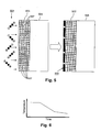
- FIGURE 5 is an example schematic view illustrating a third example technique for doping graphene in accordance with certain example embodiments
- FIGURE 6 is a graph plotting temperature vs. time involved in the doping of graphene in accordance with certain example embodiments
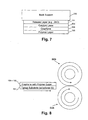
- FIGURE 8 is an example schematic view of a lamination apparatus that may be used to dispose the graphene on the target glass substrate in accordance with certain example embodiments;
- FIGURE 9 is a cross-sectional schematic view of a reactor suitable for depositing high electronic grade (HEG) graphene in accordance with an example embodiment
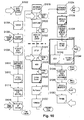
- FIGURE 10 is an example process flow that illustrates certain of the example catalytic CVD growth, lift-off, and transfer techniques of certain example embodiments;
- FIGURE 11 is an image of a sample graphene produced according to certain example embodiments.
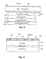
- FIGURE 12 is a cross-sectional schematic view of a solar photovoltaic device incorporating graphene-based layers according to certain example embodiments
- FIGURE 13 is a cross-sectional schematic view of a touch screen incorporating graphene-based layers according to certain example embodiments.
- FIGURE 14 is a flowchart illustrating an example technique for forming a conductive data/bus line in accordance with certain example embodiments.
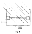
- FIGURE 15 is a schematic view of a technique for forming a conductive data/bus line in accordance with certain example embodiments.
- Certain example embodiments of this invention relate to a scalable technique to hetero-epitaxially grow mono-crystalline graphite (n as large as about 15) and convert it to high electronic grade (HEG) graphene (n ⁇ about 3). Certain example embodiments also relate to the use of HEG graphene in transparent (in terms of both visible and infrared spectra), conductive ultra-thin graphene films, e.g., as an alternative to the more ubiquitously employed metal oxides window electrodes for a variety of applications (including, for example, solid-state solar cells).
- the growth technique of certain example embodiments is based on a catalytically driven hetero-epitaxial CVD process which takes place a temperature that is low enough to be glass-friendly. For example, thermodynamic as well as kinetics principles allow HEG graphene films to be crystallized from the gas phase on a seed catalyst layer (e.g., at a temperature less than about 600 degrees C).
- Fig. 1 is a high level flowchart illustrating the overall techniques of certain example embodiments.
- the overall techniques of certain example embodiments can be classified as belonging to one of four basic steps: graphene crystallization on a suitable back support (step S101), graphene release or debonding from the back support (step S103), graphene transference to the target substrate or surface (step S105), and incorporation of the target substrate or surface into a product (step S107).
- step S101 graphene crystallization on a suitable back support
- step S103 graphene release or debonding from the back support
- step S105 graphene transference to the target substrate or surface
- step S107 incorporation of the target substrate or surface into a product
- the product referred to in step S107 may be an intermediate product or a final product.
- the graphene crystallization techniques of certain example embodiments may be thought of as involving "cracking" a hydrocarbon gas and reassembling the carbon atoms into the familiar honeycomb structure over a large area (e.g., an area of about 1 meter, or larger), e.g., leveraging the surface catalytic pathway.
- the graphene crystallization techniques of certain example embodiments take place at high temperature and moderate pressures. Illustrative details of this example process will be described in detail below.
- the catalytic growth techniques of certain example embodiments are somewhat related to the techniques that have been used to grow graphite over a hetero-epitaxial area.
- a catalyst for graphene crystallization is disposed on a suitable back support.
- the back support may be any suitable material capable of withstanding high heats (e.g., temperatures up to about 1000 degrees C) such as, for example, certain ceramics or glass products, zirconium inclusive materials, aluminum nitride materials, silicon wafers, etc.
- a thin film is disposed, directly or indirectly, on the back support, thereby ensuring that its surface is substantially uncontaminated prior to the crystallization process.
- the inventor of the instant invention has discovered that graphene crystallization is facilitated when the catalyst layer has a substantially single-orientation crystal structure.
- small grains have been determined to be less advantageous, since their mosaic structure ultimately will be transferred to the graphene layer.
- the particular orientation of the crystal structure has been found to be largely insignificant for graphene crystallization, provided that the catalyst layer, at least in substantial part, has a single-orientation crystal structure.
- the comparative absence of (or low) grain boundaries in the catalyst has been found to result in the same or a similar orientation for the grown graphene, and has been found to provide for high electrical grade (HEG) graphene.
- HOG high electrical grade
- the catalyst layer itself may be disposed on the back support by any suitable technique such as, for example, sputtering, combustion vapor deposition (CVD), flame pyrolysis, etc.
- the catalyst layer itself may comprise any suitable metal or metal-inclusive material.
- the catalyst layer may comprise, for example, metals such as nickel, cobalt, iron, permalloy (e.g., nickel iron alloys, generally comprising about 20% iron and 80% nickel), alloys of nickel and chromium, copper, and combinations thereof.
- nickel iron alloys e.g., nickel iron alloys, generally comprising about 20% iron and 80% nickel
- alloys of nickel and chromium copper, and combinations thereof.
- other metals may be used in connection with certain example embodiments.
- the inventor has discovered that catalyst layers of or including nickel are particular advantageous for graphene crystallization, and that alloys of nickel and chromium are yet more advantageous.
- the inventor has discovered that the amount of chromium in nickel-chromium layers (also sometimes called nichrome or NiCr layers) can be optimized so as to promote the formation of large crystals.
- 3-15% Cr in the NiCr layer is preferable, 5-12% Cr in the NiCr layer is more preferable, and 7-10% of Cr in the NiCr layer is still more preferable.
- the presence of vanadium in the metal thin film also has been found to be advantageous to promote large crystal growth.
- the catalyst layer may be relatively thin or thick.
- the thin film may be 50-1000 nm thick, more preferably 75-750 nm thick, and still more preferably 100-500 nm thick.
- a "large crystal growth" may in certain example instances include crystals having a length along a major axis on the order of 10s of microns, and sometimes even larger.
- a hydrocarbon gas e.g., C 2 H 2 gas, CH 4 gas, etc.
- the hydrocarbon gas may be introduced at a pressure ranging from about 5-150 mTorr, more prerferably 10-100 mTorr. In general, the higher the pressure, the faster the growth of the graphene.
- the back support and/or the chamber as a whole is/are then heated to dissolve or "crack open" the hydrocarbon gas.
- the back support may be raised to a temperature in the range of 600-1200 degrees C, more preferably 700-1000 degrees C, and still more preferably 800-900 degrees C.
- the heating may be accomplished by any suitable technique such as, for example, via a short wave infrared (IR) heater.
- the heating may take place in an environment comprising a gas such as argon, nitrogen, a mix of nitrogen and hydrogen, or other suitable environment.
- a gas such as argon, nitrogen, a mix of nitrogen and hydrogen, or other suitable environment.
- the heating of the hydrocarbon gas may take place in an environment comprising other gasses in certain example embodiments.
- it may be desirable to use a pure hydrocarbon gas for example, with C 2 H 2
- a mix of hydrocarbon gas an another inert or other gas for example, CH 4 mixed with Ar.
- the graphene will grow in this or another suitable environment.
- a quenching process may be performed using an inert gas such as, for example, argon, nitrogen, combinations thereof, etc.
- an inert gas such as, for example, argon, nitrogen, combinations thereof, etc.
- the quenching should be performed fairly quickly. More particularly, it has been found that quenching too fast or too slow results in poor or no graphene growth on the surface of the catalyst layer.
- Fig. 2 is an example schematic view of the catalytic growth techniques of certain example embodiments, illustrating the introduction of the hydrocarbon gas, the carbon dissolving, and the possible results of quenching, in accordance with certain example embodiments.
- the technique relies on the fact that the contrast of graphene may be enhanced substantially by spin coating a material onto it.
- a widely used UV curable resist e.g., PMMA
- PMMA may be spin coated, screen printed, gravure coated, or otherwise disposed on the graphene/metal/back support, e.g., at a thickness sufficient to make the film visible and continuous (e.g., around 1 micron thick).
- the inclusion of a polymer resist also may facilitate the lift-off process of the graphene prior to its transfer to the final surface. That is, in addition to providing an indication as to when graphene formation is complete, the polymer resist also may provide a support for the highly elastic graphene when the metal layer is released or otherwise debonded from the back support as explained in detail below.
- the layer can be etched down, for example, using hydrogen atoms (H*).
- H* hydrogen atoms
- This technique may be advantageous in a number of example situations. For instance, where growth occurs too quickly, unexpectedly, unevenly, etc., H* can be used to correct such problems.
- graphite may be created, graphane may be deposited, and the graphane may be selectively etched back to the desired n-level HEG graphene, e.g., using H*.
- H* can be used to selectively etch away graphene, e.g., to create conductive areas and non-conductive areas. This may be accomplished by applying an appropriate mask, performing the etching, and then removing the mask, for example.
- a sheet resistance of 150 ohms/square may be suitable for certain example applications, it will be appreciated that a further reduction in sheet resistance may be desirable for different example applications. For example, it will be appreciated that a sheet resistance of 10-20 ohms/square may be desirable for certain example applications.
- the inventor of the instant invention has determined that sheet resistance can be lowered via the doping of the graphene.
- graphene exhibits ballistic transport on a submicron scale and can be doped heavily -- either by gate voltages or molecular adsorbates or intercalates in the case where n ⁇ 2 -- without significant loss of mobility. It has been determined by the inventor of the instant invention that that in graphene, aside from the donor/acceptor distinction, there are in general two different classes of dopants, namely, paramagnetic and nonmagnetic.
- impurities act generally as rather weak dopants, whereas the paramagnetic impurities cause strong doping: Because of the linearly vanishing, electron-hole symmetric density of states (DOS) near the Dirac point of graphene, localized impurity states without spin polarization are pinned to the center of the pseudo-gap. Thus, impurity states in graphene distinguish strongly from their counterparts in usual semiconductors, where the DOS in the valence and conduction bands are very different and impurity levels lie generally far away from the middle of the gap.
- DOS electron-hole symmetric density of states
- Example dopants suitable for use in connection with certain example embodiments include nitrogen, boron, phosphorous, fluorides, lithium, potassium, ammonium, etc.
- Sulfur-based dopants e.g., sulfur dioxide
- sulfides present in glass substrates may be caused to seep out of the glass and thus dope the graphene-based layer.
- graphene doping techniques are set forth in greater detail below.
- Fig. 3 is a flowchart illustrating a first example technique for doping graphene in accordance with certain example embodiments.
- the Fig. 3 example technique essentially involves ion beam implanting the doping material in the graphene.
- graphene is grown on a metal catalyst (step S301), e.g., as described above.
- the catalyst with the graphene formed thereon is exposed to a gas comprising a material to be used as the dopant (also sometimes referred to as a dopant gas) (step S303).
- a plasma is then excited within a chamber containing the catalyst with the graphene formed thereon and the dopant gas (S305).
- An ion beam is then used to implant the dopant into the graphene (S307).
- Example ion beam techniques suitable for this sort of doping are disclosed in, for example, U.S. Patent Nos. 6,602,371 ; 6,808,606 ; and Re. 38,358 , and U.S. Publication No. 2008/0199702 , each of which is hereby incorporated herein by reference.
- the ion beam power may be about 10-200 ev, more preferably 20-50 ev, still more preferably 20-40 ev.
- dopant may be included in the glass melt.
- An ion beam also can be used to implant the dopants directly in the glass in certain example embodiments.
- the ion beam power may be about 10-1000 ev, more preferably 20-500 ev, still more preferably 20-100 ev.
- the ion beam may operate at about 10-200 ev, more preferably 20-50 ev, still more preferably 20-40 ev.
- Fig. 5 is an example schematic view illustrating a third example technique for doping graphene in accordance with certain example embodiments.
- the Fig. 5 example techniques essentially involves pre-implanting solid state dopants 507 in the metal catalyst layer 503, and then causing those solid state dopants 507 to migrate through the catalyst layer 503 as the graphene is being formed, thereby creating a doped graphene 509 on the surface of the catalyst layer 503. More particularly, in this example technique, the catalyst layer 503 is disposed on the back support 505.
- the catalyst layer 503 includes solid-state dopants 507 therein.
- example doping techniques may be used alone and/or in various combinations and sub-combinations with one another and/or further techniques. It also will be appreciated that certain example embodiments may include a single dopant material or multiple dopant materials, e.g., by using a particular example technique once, a particular technique repeatedly, or through a combination of multiple techniques one or more times each. For example, p-type and n-type dopants are possible in certain example embodiments.
- Fig. 7 is an example layer stack useful in the graphene release or debonding techniques of certain example embodiments.
- an optional release layer 701 may be provided between the back support 505 and the catalyst layer 503. This release layer 701 may be of or include, for example, zinc oxide (e.g., ZnO or other suitable stoichiometry).
- the graphene 509/metal catalyst layer 503/release layer 701 stack coated substrate 505 may receive a thick overcoat (e.g., several microns thick) layer of polymer 703, e.g., applied via spin coating, dispensed by a meniscus flow, etc., which may be cured.
- this polymer layer 703 may act as a backbone or support for the graphene 509 during lift-off and/or debonding, keeping the extremely flexible graphene film continuous, while also reducing the likelihood of the graphene film curling up, creasing, or otherwise deforming.
- Certain lift-off/debonding and transfer techniques essentially regard the original substrate as a reusable epitaxial growth substrate.
- a selective etching to undercut and dissolve away the metallic catalyst thin film away from the epitaxially grown (with polymer on top) graphene may be desirable in such example embodiments.
- the catalyst layer may be etched off, regardless of whether a release layer is used, in certain example embodiments.
- Suitable etchants include, for example, acids such as hydrochloric acid, phosphoric acid, etc.
- the final recipient glass substrate surface may be prepared so as to receive the graphene layer.
- a Langmuir Blodgett film e.g., from a Langmuir-Blodgett acid
- the final recipient substrate alternatively or additionally may be coated with a smooth graphenophillic layer such as, for example, a silicone-based polymer, etc., making the latter receptive to the graphene. This may help to ensure electrostatic bonding, thus preferentially allowing the transfer of the graphene during transfer.
- the target substrate may additionally or alternatively be exposed to UV radiation, e.g., to increase the surface energy of the target substrate and thus make it more receptive to the graphene.
- the graphene may be applied to the substrate via blanket stamping and/or rolling in certain example embodiments. Such processes allow the graphene previously grown and chemisorbed onto the metal carrier to be transferred onto the recipient glass by contact pressure.
- the graphene may be applied to the substrate via one or more lamination rollers, e.g., as shown in Fig. 8 .
- Fig. 8 shows upper and lower rollers 803a and 803b, which will apply pressure and cause the graphene 509 and polymer layer 703 to be laminated to the target substrate 801.
- the target substrate 801 have a silicon-inclusive or other graphenophillic layer disposed thereon to facilitate the lamination.
- the polymer layer 703 will be applied as the outermost layer and that the graphene 509 will be closer to (or even directly on) the target substrate 801.
- one or more layers may be provided on the substrate prior to the application of the graphene.
- the polymer layer may be removed.
- the polymer may be dissolved using an appropriate solvent.
- a photosensitive material such as PMMA
- it may be removed via UV light exposure. Of course, other removal techniques also are possible.
- the catalyst thin film may be etched off after the graphene has been applied to the target substrate in certain example embodiments, e.g., using one of the example etchants described above.
- the choice of etchant also may be based on the presence or absence of any layers underlying the graphene.
- cobalt, chrome cobalt, nickel chrome cobalt, and/or the like may be oxidized. In certain example embodiments, this may also reduce the need for graphene lift-off, making the transfer, manipulation, and other handling of graphene easier.
- the graphene also may be picked up using an adhesive or tape-like material in certain example embodiments.
- the adhesive may be positioned on the target substrate.
- the graphene may be transferred to the target substrate, e.g., following the application of pressure, by more strongly adhering to the substrate than to the tape, etc.
- two exhaust ports 905 are provided proximate to the extremes of the body portion 901 of the reactor, e.g., so as to draw out gas provided by the gas inlet 903 that generally will flow through substantially the entirety of the body portion 901. It will be appreciated that more or fewer exhaust ports 905 may be provided in certain example embodiments (e.g., further exhaust ports 905 may be provided in the approximate horizontal center of the body portion 901 of the reactor, at the top or sides of the body portion 901 of the reactor, etc.).
- the back support substrate 909 may be cleaned and have the catalyst thin film disposed thereon (e.g., by physical vapor deposition or PVD, sputtering, CVD, flame pyrolysis, or the like) prior to entry into the reactor by a load-lock mechanism in certain example embodiments.
- the catalyst thin film disposed thereon (e.g., by physical vapor deposition or PVD, sputtering, CVD, flame pyrolysis, or the like) prior to entry into the reactor by a load-lock mechanism in certain example embodiments.
- the surface of the back support substrate 909 may be rapidly heated (e.g., using an RTA heater, a shortwave IR heater, or other suitable heater that is capable of inductively heating the substrate and/or layers thereon without necessarily also heating the entire chamber) to a controllable temperature level and uniformity that allows (i) the metal film to crystallize and activate, and (ii) the preferential deposition of graphene of substantially uniform and controllable thickness from a gas phase precursor on its surface.
- the heater may be controllable so as to account for the parameter deposition rate/(temperature * thickness) of catalyst ratio.
- the back support substrate 909 may move through the reactor in the direction R or may sit stationary under the showerhead 907.
- the showerhead 907 may be cooled, e.g., using a cooling fluid or gas introduced by one or more coolant inlets/outlets 913.
- the plenum design may include a plurality of apertures in the bottom of the showerhead 907, with each such aperture being only a few millimeters wide.
- Changing the ceiling gap Hc, or the height between the bottom surface of the showerhead 907 and the top surface upon which the back support substrate 909 moves, may have several effects.
- the chamber volume and thus the surface-to-volume ratio may be modified, thereby affecting the gas residence time, consumption time, and radial velocities. Changes in the residence time have been found to strongly influence the extent of gas phase reactions.
- the ceiling gap Hc may be varied through simple hardware changes, by providing adjustable mounting of the substrate electrode, etc., so as to affect the hetero-epitaxial growth of the graphene.
- the Fig. 9 example embodiment is not necessarily intended to operate a plasma within the reactor. This is because the crystalline film growth mechanism is by hetero-epitaxy by surface sorption (generally occurring only on the catalyst). Growth from the plasma phase has been found to give rise to mostly amorphous films and also has been found to allow the formation of macro-particle or dust formation that can greatly reduce film quality and result in pinholes that would be detrimental for a one-to-ten atomic layer film.
- certain example embodiments may involve making graphite (e.g., monocrystalline graphite), etching it to graphane (e.g., of a certain n-value), and turning the graphane into graphene (e.g., into HEG graphene).
- an in-situ end-point technique may be implemented as a feedback parameter.
- an ion beam source may be located in-line but external to the reactor of Fig. 9 , e.g., to perform doping in accordance with the example techniques described above. However, in certain example embodiments, an ion beam source may be located within the body portion of a reactor.
- Fig. 10 is an example process flow that illustrates certain of the example catalytic CVD growth, lift-off, and transfer techniques of certain example embodiments.
- the example process shown in Fig. 10 begins as the back support glass is inspected, e.g., using a conventional glass inspection method (step S1002) and washed (step S1004).
- the back support glass may then be cleaned using ion beam cleaning, plasma ashing, or the like (step S1006).
- the catalyst e.g., a metal catalyst
- step S 1006 may be accomplished within the graphene coater/reactor in certain example embodiments of this invention.
- the back support glass with or without the metal catalyst thin film formed thereon may be loaded into the graphene coater/reactor prior to step S 1006 in certain example embodiments, e.g., depending on whether the metal catalyst layer is deposited within or prior to the coater/reactor.
- the catalytic deposition of an n-layer graphene may then take place (step S1010).
- the graphene may be etched down by introducing hydrogen atoms (H*) in certain example embodiments, and the graphene optionally may be doped, e.g., depending on the target application (step S1012).
- the end of the graphene formation is detected, e.g., by determining whether enough graphene has been deposited and/or whether the H* etching has been sufficient (step S1014).
- a rapid quenching process is used, and the back support glass with the graphene formed therein exits the reactor/coater (step S1016). Visual inspection optionally may be performed at this point.
- a polymer useful in the transference of the graphene may be disposed on the graphene, e.g., by spin, blade, or other coating technique (step S1018).
- This product optionally may be inspected, e.g., to determine whether the requisite color change takes place. If it has, the polymer may be cured (e.g., using heat, UV radiation, etc.) (step S1020), and then inspected again.
- the metal catalyst may be under-etched or otherwise released (step S1022), e.g., to prepare the graphene for lift-off (step S1024).
- the recipient substrate is prepared (step S1034), e.g., in a clean room.
- the surface of the recipient substrate may be functionalized, e.g., by exposing it to a UV light to increase its surface energy, to apply graphenophillic coatings thereto, etc. (step S1036).
- the graphene / polymer membrane may then be transferred onto the host substrate (step S1038).
- the receiving substrate with the graphene and polymer attached thereto may be fed into a module to remove the polymer (step S1040). This may be done by exposing the polymer to UV light, heat, chemicals, etc.
- the substrate with the graphene and at least partially dissolved polymer may then be washed (step S1042), with any excess water or other materials evaporated and dried off (step S1044). This polymer removal process may be repeated, as necessary.
- Fig. 11 is an image of a sample graphene produced according to certain example embodiments.
- the Fig. 11 image highlights the lift-off of the hetero-epitaxially grown graphene from a permalloy thin film.
- graphene-based layers may be used in a wide variety of applications and/or electronic devices.
- ITO and/or other conductive layers simply may be replaced by graphene-based layers.
- Making devices with graphene will typically involve making contacts with metals, degenerate semiconductors like ITO, solar cell semiconductors such as a-Si and CdTe among others, and/or the like.
- the graphene-based layer may be doped in accordance with any semiconductor layers adjacent thereto. That is, in certain example embodiments, if a graphene-based layer is adjacent to an n-type semiconductor layer, the graphene-based layer may be doped with an n-type dopant.
- a graphene-based layer if a graphene-based layer is adjacent to a p-type semiconductor layer, the graphene-based layer may be doped with a p-type dopant.
- DFT -density functional theory
- a first example electronic device that may make use of one or more graphene-based layers is a solar photovoltaic device.
- Such example devices may include front electrodes or back electrodes.
- the graphene-based layers may simply replace the ITO typically used therein.
- Photovoltaic devices are disclosed in, for example, U.S. Patent Nos. 6,784,361 , 6,288,325 , 6,613,603 and 6,123,824 ; U.S. Publication Nos. 2008/0169021 ; 2009/0032098 ; 2008/0308147 ; and 2009/0020157 ; and Application Serial Nos. 12/285,374 , 12/285,890 , and 12/457,006 , the disclosures of which are hereby incorporated herein by reference.
- Fig. 12 is a cross-sectional schematic view of a solar photovoltaic device incorporating graphene-based layers according to certain example embodiments.
- a glass substrate 1202 is provided.
- the glass substrate 1202 may be of any of the glasses described in any of U.S. Patent Application Serial Nos. 11/049,292 and/or 11/122,218, the disclosures of which are hereby incorporated herein by reference.
- the glass substrate optionally may be nano-textured, e.g., to increase the efficiency of the solar cell.
- An anti-reflective (AR) coating 1204 may be provided on an exterior surface of the glass substrate 1202, e.g., to increase transmission.
- the anti-reflective coating 1204 may be a single-layer anti-reflective (SLAR) coating (e.g., a silicon oxide anti-reflective coating) or a multi-layer anti-reflective (MLAR) coating.
- SLAR single-layer anti-reflective
- MLAR multi-layer anti-reflective
- One or more absorbing layers 1206 may be provided on the glass substrate 1202 opposite the AR coating 1204, e.g., in the case of a back electrode device such as that shown in the Fig. 12 example embodiment.
- the absorbing layers 1206 may be sandwiched between first and second semi-conductors.
- absorbing layers 1206 are sandwiched between n-type semiconductor layer 1208 (closer to the glass substrate 1202) and p-type semiconductor 1210 (farther from the glass substrate 1202).
- a back contact 1212 e.g., of aluminum or other suitable material also may be provided.
- first and second graphene-based layers 1214 and 1216 may be provided.
- the graphene-based layers 1214 and 1216 may be doped so as to match the adjacent semiconductor layers 1208 and 1210, respectively.
- graphene-based layer 1214 may be doped with n-type dopants and graphene-based layer 1216 may be doped with p-type dopants.
- graphene is essentially transparent in the near and mid-IR ranges implies that the most penetrating long wavelength radiation may penetrate and generate carriers deep into the i-layer of both single and tandem junction solar cells. This implies that the need to texture back contacts may not be needed with graphene-based layers, as the efficiency will already be increased by as much as several percentage points.
- Certain example embodiments may involve single-junction solar cells, whereas certain example embodiments may involve tandem solar cells.
- Certain example embodiments may be CdS, CdTe, CIS/ CIGS, a-Si, and/or other types of solar cells.
- the touch panel display may be a capacitive or resistive touch panel display including ITO or other conductive layers. See, for example, U.S. Patent Nos. 7,436,393 ; 7,372,510 ; 7,215,331 ; . 6,204,897 ; 6,177,918 ; and 5,650,597 , and Application Serial No. 12/292,406 , the disclosures of which are hereby incorporated herein by reference.
- the ITO and/or other conductive layers may be replaced in such touch panels may be replaced with graphene-based layers. For example, Fig.
- Fig. 13 is a cross-sectional schematic view of a touch screen incorporating graphene-based layers according to certain example embodiments.
- Fig. 13 includes an underlying display 1302, which may, in certain example embodiments, be an LCD, plasma, or other flat panel display.
- An optically clear adhesive 1304 couples the display 1302 to a thin glass sheet 1306.
- a deformable PET foil 1308 is provided as the top-most layer in the Fig. 13 example embodiment.
- the PET foil 1308 is spaced apart from the upper surface of the thin glass substrate 1306 by virtual of a plurality of pillar spacers 1310 and edge seals 1312.
- First and second graphene-based layers 1314 and 1316 may be provided on the surface of the PET foil 1308 closer to the display 1302 and to the thin glass substrate 1306 on the surface facing the PET foil 1308, respectively.
- One or both graphene-based layers 1314 and 1316 may be patterned, e.g., by ion beam and/or laser etching. It is noted that the graphene-based layer on the PET foil may be transferred from its growth location to the intermediate product using the PET foil itself. In other words, the PET foil may be used instead of a photoresist or other material when lifting off the graphene and/or moving it.
- a sheet resistance of less than about 500 ohms/square for the graphene-based layers is acceptable in embodiments similar to those shown in Fig. 13 , and a sheet resistance of less than about 300 ohms/square is advantageous for the graphene-based layers.
- Graphene-based layers also may be used to create conductive data/bus lines, bus bars, antennas, and/or the like: Such structures may be formed on/applied to glass substrates, silicon wafers, etc.
- Fig. 14 is a flowchart illustrating an example technique for forming a conductive data/bus line in accordance with certain example embodiments.
- step S1401 a graphene-based layer is formed on an appropriate substrate.
- a protective layer may be provided over the graphene-based layer.
- the graphene-based layer is selectively removed or patterned. This removal or patterning may be accomplished by laser etching.
- etching may be performed via exposure to an ion beam/plasma treatment.
- H* may be used, e.g., in connection with a hot filament.
- a protective layer may be desirable.
- a photoresist material may be used to protect the graphene areas of interest.
- Such a photoresist may be applied, e.g., by spin coating or the like in step S 1403.
- the optional protective layer is removed. Exposure to UV radiation may be used with appropriate photoresists, for example.
- the conductive graphene-based pattern may be transferred to an intermediate or final product if it was not already formed thereon, e.g., using any appropriate technique (such as, for example, those described above).
- certain example embodiments have been described as etching away or removing graphene-based layers, certain example embodiments may simply change the conductivity of the graphene-based layer. In such cases, some or all of the graphene may not be removed. However, because the conductivity has been suitably altered, only the appropriately patterned areas may be conductive.
- Mobility data is shown in the table below after various samples have been deposited and etched. Etched Samples Passes Thickness (A) Rho ( ⁇ cm) Conductivty (1/ ⁇ cm) Mobility ⁇ (cm ⁇ 2/ Vs) A 25 8 1.03E-04 970000 120,000 B 20 6 5.24E-03 1010000 143000 C 10 6 5.94E-02 1600000 150000 D 5 6 1.48E-02 1500000 160000
- the layer will be largely transparent.
- bus bars that may be incorporated into vehicle windows (e.g., for defrosting, antenna usage, powering components, etc.), flat panel (e.g., LCD, plasma, and/or other) display devices, skylights, refrigerator/freezer doors/windows, etc. This may also advantageously reduce the need for black frits often found in such products.
- graphene-based layers may be used in place of ITO in electrochromic devices.
Landscapes
- Chemical & Material Sciences (AREA)
- Engineering & Computer Science (AREA)
- Organic Chemistry (AREA)
- Materials Engineering (AREA)
- Crystallography & Structural Chemistry (AREA)
- Nanotechnology (AREA)
- Metallurgy (AREA)
- Chemical Kinetics & Catalysis (AREA)
- General Chemical & Material Sciences (AREA)
- General Physics & Mathematics (AREA)
- Condensed Matter Physics & Semiconductors (AREA)
- Physics & Mathematics (AREA)
- Inorganic Chemistry (AREA)
- Manufacturing & Machinery (AREA)
- Composite Materials (AREA)
- Carbon And Carbon Compounds (AREA)
- Drying Of Semiconductors (AREA)
- Catalysts (AREA)
Applications Claiming Priority (2)
| Application Number | Priority Date | Filing Date | Title |
|---|---|---|---|
| US12/461,346 US10167572B2 (en) | 2009-08-07 | 2009-08-07 | Large area deposition of graphene via hetero-epitaxial growth, and products including the same |
| EP10737395A EP2462262A2 (de) | 2009-08-07 | 2010-07-15 | Grossflächige abscheidung von heteroepitaxial gezüchtetem graphen sowie produkte damit |
Related Parent Applications (1)
| Application Number | Title | Priority Date | Filing Date |
|---|---|---|---|
| EP10737395.3 Division | 2010-07-15 |
Publications (2)
| Publication Number | Publication Date |
|---|---|
| EP2584072A2 true EP2584072A2 (de) | 2013-04-24 |
| EP2584072A3 EP2584072A3 (de) | 2013-07-10 |
Family
ID=42797336
Family Applications (2)
| Application Number | Title | Priority Date | Filing Date |
|---|---|---|---|
| EP10737395A Withdrawn EP2462262A2 (de) | 2009-08-07 | 2010-07-15 | Grossflächige abscheidung von heteroepitaxial gezüchtetem graphen sowie produkte damit |
| EP13151830.0A Withdrawn EP2584072A3 (de) | 2009-08-07 | 2010-07-15 | Grossflächige Abscheidung von heteroepitaxial gezüchtetem Graphen und Produkte damit |
Family Applications Before (1)
| Application Number | Title | Priority Date | Filing Date |
|---|---|---|---|
| EP10737395A Withdrawn EP2462262A2 (de) | 2009-08-07 | 2010-07-15 | Grossflächige abscheidung von heteroepitaxial gezüchtetem graphen sowie produkte damit |
Country Status (12)
| Country | Link |
|---|---|
| US (1) | US10167572B2 (de) |
| EP (2) | EP2462262A2 (de) |
| JP (1) | JP5731502B2 (de) |
| KR (1) | KR101724772B1 (de) |
| CN (2) | CN109023514A (de) |
| BR (1) | BR112012008091A2 (de) |
| IN (1) | IN2012DN00856A (de) |
| MX (1) | MX338878B (de) |
| RU (1) | RU2012108641A (de) |
| SA (1) | SA110310637B1 (de) |
| TW (1) | TW201114683A (de) |
| WO (1) | WO2011016828A2 (de) |
Families Citing this family (58)
| Publication number | Priority date | Publication date | Assignee | Title |
|---|---|---|---|---|
| GB201004554D0 (en) * | 2010-03-18 | 2010-05-05 | Isis Innovation | Superconducting materials |
| US20120068161A1 (en) * | 2010-09-16 | 2012-03-22 | Lee Keon-Jae | Method for forming graphene using laser beam, graphene semiconductor manufactured by the same, and graphene transistor having graphene semiconductor |
| CN102127750B (zh) * | 2011-03-01 | 2012-08-22 | 哈尔滨工程大学 | 一种基于化学沉积法制备石墨烯材料的方法 |
| KR101806916B1 (ko) * | 2011-03-17 | 2017-12-12 | 한화테크윈 주식회사 | 그래핀 필름 제조 장치 및 그래핀 필름 제조 방법 |
| KR101842018B1 (ko) * | 2011-04-01 | 2018-03-26 | 한화테크윈 주식회사 | 그래핀을 포함하는 필름 제조 방법 |
| US8739728B2 (en) * | 2011-04-07 | 2014-06-03 | Dynamic Micro Systems, Semiconductor Equipment Gmbh | Methods and apparatuses for roll-on coating |
| JP5562283B2 (ja) * | 2011-04-07 | 2014-07-30 | 日本写真印刷株式会社 | グラフェンを主成分とする透明導電膜を備えた透明導電物とその製造方法 |
| JP5455963B2 (ja) * | 2011-04-07 | 2014-03-26 | 日本写真印刷株式会社 | グラフェンを主成分とする透明導電膜を備えた転写シートとその製造方法 |
| JP5541741B2 (ja) * | 2011-04-11 | 2014-07-09 | 日本写真印刷株式会社 | グラフェンを主成分とする透明導電膜を備えた転写シートとその製造方法 |
| CN102719877B (zh) * | 2011-06-09 | 2014-09-03 | 中国科学院金属研究所 | 一种低成本无损转移石墨烯的方法 |
| KR101380835B1 (ko) * | 2011-07-22 | 2014-04-04 | 성균관대학교산학협력단 | 그래핀의 원자층 식각 방법 |
| CN102296361B (zh) * | 2011-09-05 | 2013-09-25 | 电子科技大学 | 一种单晶石墨烯的制备方法 |
| KR20140092809A (ko) | 2011-09-09 | 2014-07-24 | 보드 오브 트러스티즈 오브 노선 일리노이스 유니버시티 | 결정성 그래핀 및 결정성 그래핀 제조 방법 |
| KR101878739B1 (ko) | 2011-10-24 | 2018-07-17 | 삼성전자주식회사 | 그래핀 전사부재, 그래핀 전사방법 및 이를 이용한 그래핀 소자 제조방법 |
| JP5851804B2 (ja) * | 2011-11-09 | 2016-02-03 | 東京エレクトロン株式会社 | 前処理方法、グラフェンの形成方法及びグラフェン製造装置 |
| SG10201908213VA (en) * | 2012-02-24 | 2019-10-30 | California Inst Of Techn | Method and system for graphene formation |
| US9527043B2 (en) * | 2012-05-17 | 2016-12-27 | Samsung Electronics Co., Ltd. | Gas separation membrane and method of preparing the same |
| KR101920716B1 (ko) | 2012-05-17 | 2019-02-13 | 삼성전자주식회사 | 기체 분리막 및 그 제조방법 |
| EP2679540A1 (de) * | 2012-06-29 | 2014-01-01 | Graphenea, S.A. | Verfahren zur Herstellung einer Grapheneinzelschicht auf Isolationssubstraten |
| CN103572247A (zh) * | 2012-07-27 | 2014-02-12 | 中国科学院苏州纳米技术与纳米仿生研究所 | 一种在金属催化剂表面制备薄层石墨烯的方法 |
| CN102774118B (zh) * | 2012-07-31 | 2015-05-13 | 无锡格菲电子薄膜科技有限公司 | 一种以静电保护膜为媒介转移石墨烯薄膜的方法 |
| PL224447B1 (pl) | 2012-08-25 | 2016-12-30 | Advanced Graphene Products Spółka Z Ograniczoną Odpowiedzialnością | Sposób oddzielania grafenu od ciekłej matrycy formującej |
| WO2014055040A1 (en) * | 2012-10-03 | 2014-04-10 | National University Of Singapore | Touch screen devices employing graphene networks with polyvinylidene fluoride films |
| CN102903617B (zh) * | 2012-10-22 | 2015-09-09 | 西安电子科技大学 | 基于GaN衬底的石墨烯CVD直接外延生长方法及制造的器件 |
| CN102903616A (zh) * | 2012-10-22 | 2013-01-30 | 西安电子科技大学 | 基于ZnO衬底的石墨烯CVD直接外延生长方法及制造的器件 |
| CN102903618B (zh) * | 2012-10-22 | 2015-07-29 | 西安电子科技大学 | 基于AlN衬底的石墨烯CVD直接外延生长方法及制造的器件 |
| US9595436B2 (en) | 2012-10-25 | 2017-03-14 | Applied Materials, Inc. | Growing graphene on substrates |
| CN104995332B (zh) * | 2012-11-19 | 2017-08-08 | 加利福尼亚大学董事会 | 基于石墨烯的电极及应用 |
| US10315275B2 (en) * | 2013-01-24 | 2019-06-11 | Wisconsin Alumni Research Foundation | Reducing surface asperities |
| US10163576B2 (en) * | 2013-02-06 | 2018-12-25 | Apaq Technology Co., Ltd. | Capacitor cathode foil structure and manufacturing method thereof |
| KR102049487B1 (ko) * | 2013-03-08 | 2019-11-28 | 삼성디스플레이 주식회사 | 표시 장치의 제조 방법 |
| US10431354B2 (en) * | 2013-03-15 | 2019-10-01 | Guardian Glass, LLC | Methods for direct production of graphene on dielectric substrates, and associated articles/devices |
| US9593019B2 (en) | 2013-03-15 | 2017-03-14 | Guardian Industries Corp. | Methods for low-temperature graphene precipitation onto glass, and associated articles/devices |
| JP6002087B2 (ja) * | 2013-05-29 | 2016-10-05 | 東京エレクトロン株式会社 | グラフェンの生成方法 |
| ES2589793T3 (es) | 2013-10-28 | 2016-11-16 | Advanced Graphene Products Sp. Z O. O. | Procedimiento de producción de grafeno sobre un metal líquido |
| US9284640B2 (en) | 2013-11-01 | 2016-03-15 | Advanced Graphene Products Sp. Z.O.O. | Method of producing graphene from liquid metal |
| JP6353308B2 (ja) * | 2014-07-24 | 2018-07-04 | 株式会社カネカ | 配線材料、配線材料の製造方法、および配線材料を用いた配線板の製造方法 |
| CN104409177B (zh) * | 2014-11-28 | 2017-02-22 | 中国科学院金属研究所 | 一种稳定掺杂的大面积石墨烯透明导电膜规模化制备方法 |
| JP6190562B2 (ja) * | 2015-03-26 | 2017-08-30 | 中国科学院上海微系統与信息技術研究所 | グラフェンの成長方法 |
| US10133428B2 (en) * | 2015-05-29 | 2018-11-20 | Samsung Display Co., Ltd. | Flexible display device including a flexible substrate having a bending part and a conductive pattern at least partially disposed on the bending part |
| GB201514542D0 (en) | 2015-08-14 | 2015-09-30 | Thomas Simon C S | A method of producing graphene |
| US10145005B2 (en) | 2015-08-19 | 2018-12-04 | Guardian Glass, LLC | Techniques for low temperature direct graphene growth on glass |
| JP6440850B2 (ja) | 2015-09-02 | 2018-12-19 | 東京エレクトロン株式会社 | グラフェンの製造方法、グラフェンの製造装置及び電子デバイスの製造方法 |
| US9666615B2 (en) | 2015-10-20 | 2017-05-30 | International Business Machines Corporation | Semiconductor on insulator substrate with back bias |
| RU2614289C1 (ru) * | 2015-11-10 | 2017-03-24 | Федеральное государственное бюджетное учреждение науки Институт проблем технологии микроэлектроники и особочистых материалов Российской академии наук (ИПТМ РАН) | Способ получения пленки графена на подложке |
| US10190211B2 (en) * | 2015-11-20 | 2019-01-29 | Fourté International, Sdn. Bhd | High conductivity graphane-metal and graphene-metal composite and methods of manufacture |
| US20230275229A1 (en) * | 2015-11-23 | 2023-08-31 | Tereza M. Paronyan | Graphene networks and methods for synthesis and use of the same |
| US11718529B1 (en) * | 2015-11-23 | 2023-08-08 | Paronyan Tereza M | Graphene networks and methods for synthesis and use of the same |
| US20170155985A1 (en) * | 2015-11-30 | 2017-06-01 | Bragi GmbH | Graphene Based Mesh for Use in Portable Electronic Devices |
| DE112018000257T5 (de) * | 2017-01-11 | 2019-09-12 | Baker Hughes, A Ge Company, Llc | Dünne filmsubstrate einschliesslich vernetzter kohlenstoffnanostrukturen und verwandte verfahren |
| JP7303795B2 (ja) | 2017-08-22 | 2023-07-05 | インサーマ コーポレーション | グラフェンナノリボン、グラフェンナノプレートレット及びこれらの混合物並びに合成の方法 |
| JP6960813B2 (ja) | 2017-09-20 | 2021-11-05 | 東京エレクトロン株式会社 | グラフェン構造体の形成方法および形成装置 |
| GB2570126B (en) * | 2018-01-11 | 2022-07-27 | Paragraf Ltd | Graphene based contact layers for electronic devices |
| CN110697861A (zh) * | 2019-11-13 | 2020-01-17 | 孙晓阳 | 活性光解微晶及其制备方法 |
| US11515163B2 (en) * | 2021-01-06 | 2022-11-29 | Applied Materials, Inc. | Low temperature graphene growth |
| JP7600879B2 (ja) * | 2021-06-03 | 2024-12-17 | 富士通株式会社 | 多層グラフェンの製造方法 |
| CN114228182B (zh) * | 2021-12-24 | 2024-05-31 | 中科合肥智慧农业协同创新研究院 | 一种快速制备石墨烯三明治型光热转换地膜的方法 |
| CN119314869A (zh) * | 2024-08-26 | 2025-01-14 | 湖南大学 | 图案化的二维VX2、横向、垂直VX2/TMDs异质结及其制备和应用 |
Citations (1)
| Publication number | Priority date | Publication date | Assignee | Title |
|---|---|---|---|---|
| US20090155561A1 (en) * | 2007-12-17 | 2009-06-18 | Samsung Electronics Co., Ltd. | Single crystalline graphene sheet and process of preparing the same |
Family Cites Families (111)
| Publication number | Priority date | Publication date | Assignee | Title |
|---|---|---|---|---|
| US4929205A (en) | 1988-10-07 | 1990-05-29 | Jones Elene K | Leg immobilizer-drag for training swimmers |
| US5227038A (en) * | 1991-10-04 | 1993-07-13 | William Marsh Rice University | Electric arc process for making fullerenes |
| US5300203A (en) * | 1991-11-27 | 1994-04-05 | William Marsh Rice University | Process for making fullerenes by the laser evaporation of carbon |
| US5591312A (en) * | 1992-10-09 | 1997-01-07 | William Marsh Rice University | Process for making fullerene fibers |
| DE4313481A1 (de) * | 1993-04-24 | 1994-10-27 | Hoechst Ag | Fullerenderivate, Verfahren zur Herstellung und deren Verwendung |
| WO1995000440A1 (en) * | 1993-06-28 | 1995-01-05 | William Marsh Rice University | Solar process for making fullerenes |
| US5650597A (en) * | 1995-01-20 | 1997-07-22 | Dynapro Systems, Inc. | Capacitive touch sensor |
| US6162926A (en) * | 1995-07-31 | 2000-12-19 | Sphere Biosystems, Inc. | Multi-substituted fullerenes and methods for their preparation and characterization |
| US6183714B1 (en) * | 1995-09-08 | 2001-02-06 | Rice University | Method of making ropes of single-wall carbon nanotubes |
| US7338915B1 (en) * | 1995-09-08 | 2008-03-04 | Rice University | Ropes of single-wall carbon nanotubes and compositions thereof |
| WO1998005920A1 (en) * | 1996-08-08 | 1998-02-12 | William Marsh Rice University | Macroscopically manipulable nanoscale devices made from nanotube assemblies |
| US6123824A (en) * | 1996-12-13 | 2000-09-26 | Canon Kabushiki Kaisha | Process for producing photo-electricity generating device |
| JPH10178195A (ja) | 1996-12-18 | 1998-06-30 | Canon Inc | 光起電力素子 |
| ATE299474T1 (de) | 1997-03-07 | 2005-07-15 | Univ Rice William M | Kohlenstofffasern ausgehend von einwandigen kohlenstoffnanoröhren |
| US6683783B1 (en) * | 1997-03-07 | 2004-01-27 | William Marsh Rice University | Carbon fibers formed from single-wall carbon nanotubes |
| JPH1146006A (ja) * | 1997-07-25 | 1999-02-16 | Canon Inc | 光起電力素子およびその製造方法 |
| US6129901A (en) * | 1997-11-18 | 2000-10-10 | Martin Moskovits | Controlled synthesis and metal-filling of aligned carbon nanotubes |
| GB9806066D0 (en) | 1998-03-20 | 1998-05-20 | Cambridge Display Tech Ltd | Multilayer photovoltaic or photoconductive devices |
| CA2335449A1 (en) * | 1998-06-19 | 1999-12-23 | The Research Foundation Of The State University Of New York | Free-standing and aligned carbon nanotubes and synthesis thereof |
| US6077722A (en) * | 1998-07-14 | 2000-06-20 | Bp Solarex | Producing thin film photovoltaic modules with high integrity interconnects and dual layer contacts |
| US6057903A (en) * | 1998-08-18 | 2000-05-02 | International Business Machines Corporation | Liquid crystal display device employing a guard plane between a layer for measuring touch position and common electrode layer |
| US6204897B1 (en) * | 1998-08-18 | 2001-03-20 | International Business Machines Corporation | Integrated resistor for measuring touch position in a liquid crystal display device |
| US7150864B1 (en) | 1998-09-18 | 2006-12-19 | William Marsh Rice University | Ropes comprised of single-walled and double-walled carbon nanotubes |
| DE69941294D1 (de) * | 1998-09-18 | 2009-10-01 | Univ Rice William M | Chemische derivatisierung von einwandigen kohlenstoffnanoröhren um ihre solvatation zu erleichtern und verwendung derivatisierter nanoröhren |
| US6692717B1 (en) * | 1999-09-17 | 2004-02-17 | William Marsh Rice University | Catalytic growth of single-wall carbon nanotubes from metal particles |
| CA2344180C (en) | 1998-09-18 | 2008-04-29 | William Marsh Rice University | Catalytic growth of single-wall carbon nanotubes from metal particles |
| US6835366B1 (en) | 1998-09-18 | 2004-12-28 | William Marsh Rice University | Chemical derivatization of single-wall carbon nanotubes to facilitate solvation thereof, and use of derivatized nanotubes |
| JP4619539B2 (ja) * | 1998-11-03 | 2011-01-26 | ウィリアム・マーシュ・ライス・ユニバーシティ | 高温一酸化炭素気体からの単層カーボンナノチューブの結晶核形成および成長 |
| US6808606B2 (en) * | 1999-05-03 | 2004-10-26 | Guardian Industries Corp. | Method of manufacturing window using ion beam milling of glass substrate(s) |
| CN100366528C (zh) * | 1999-10-27 | 2008-02-06 | 威廉马歇莱思大学 | 碳质毫微管的宏观有序集合体 |
| US7195780B2 (en) * | 2002-10-21 | 2007-03-27 | University Of Florida | Nanoparticle delivery system |
| US20020048632A1 (en) * | 2000-08-24 | 2002-04-25 | Smalley Richard E. | Polymer-wrapped single wall carbon nanotubes |
| US6359388B1 (en) * | 2000-08-28 | 2002-03-19 | Guardian Industries Corp. | Cold cathode ion beam deposition apparatus with segregated gas flow |
| US6784361B2 (en) * | 2000-09-20 | 2004-08-31 | Bp Corporation North America Inc. | Amorphous silicon photovoltaic devices |
| US7052668B2 (en) * | 2001-01-31 | 2006-05-30 | William Marsh Rice University | Process utilizing seeds for making single-wall carbon nanotubes |
| US6913789B2 (en) * | 2001-01-31 | 2005-07-05 | William Marsh Rice University | Process utilizing pre-formed cluster catalysts for making single-wall carbon nanotubes |
| US6752977B2 (en) * | 2001-02-12 | 2004-06-22 | William Marsh Rice University | Process for purifying single-wall carbon nanotubes and compositions thereof |
| US7090819B2 (en) * | 2001-02-12 | 2006-08-15 | William Marsh Rice University | Gas-phase process for purifying single-wall carbon nanotubes and compositions thereof |
| US6602371B2 (en) * | 2001-02-27 | 2003-08-05 | Guardian Industries Corp. | Method of making a curved vehicle windshield |
| KR20010094773A (ko) | 2001-03-16 | 2001-11-03 | 장광식 정윤철 | 편광판 일체형 터치 패널 및 터치 패널 일체형 평판디스플레이 그리고 적층 방법 |
| US7265174B2 (en) * | 2001-03-22 | 2007-09-04 | Clemson University | Halogen containing-polymer nanocomposite compositions, methods, and products employing such compositions |
| US6890506B1 (en) * | 2001-04-12 | 2005-05-10 | Penn State Research Foundation | Method of forming carbon fibers |
| US7014737B2 (en) * | 2001-06-15 | 2006-03-21 | Penn State Research Foundation | Method of purifying nanotubes and nanofibers using electromagnetic radiation |
| US7125502B2 (en) | 2001-07-06 | 2006-10-24 | William Marsh Rice University | Fibers of aligned single-wall carbon nanotubes and process for making the same |
| DE60229955D1 (de) * | 2001-08-29 | 2009-01-02 | Georgia Tech Res Inst | Zusammensetzungen, welche stäbchenförmige polymere und nanoröhrenförmige strukturen umfassen, sowie verfahren zur herstellung derselben |
| US6538153B1 (en) * | 2001-09-25 | 2003-03-25 | C Sixty Inc. | Method of synthesis of water soluble fullerene polyacids using a macrocyclic malonate reactant |
| DE10228523B4 (de) * | 2001-11-14 | 2017-09-21 | Lg Display Co., Ltd. | Berührungstablett |
| US7138100B2 (en) * | 2001-11-21 | 2006-11-21 | William Marsh Rice Univesity | Process for making single-wall carbon nanotubes utilizing refractory particles |
| US7338648B2 (en) * | 2001-12-28 | 2008-03-04 | The Penn State Research Foundation | Method for low temperature synthesis of single wall carbon nanotubes |
| TW200307563A (en) * | 2002-02-14 | 2003-12-16 | Sixty Inc C | Use of BUCKYSOME or carbon nanotube for drug delivery |
| WO2003075207A2 (en) * | 2002-03-01 | 2003-09-12 | Planar Systems, Inc. | Reflection resistant touch screens |
| WO2003084869A2 (en) * | 2002-03-04 | 2003-10-16 | William Marsh Rice University | Method for separating single-wall carbon nanotubes and compositions thereof |
| US6936653B2 (en) * | 2002-03-14 | 2005-08-30 | Carbon Nanotechnologies, Inc. | Composite materials comprising polar polymers and single-wall carbon nanotubes |
| US6899945B2 (en) * | 2002-03-19 | 2005-05-31 | William Marsh Rice University | Entangled single-wall carbon nanotube solid material and methods for making same |
| US7192642B2 (en) * | 2002-03-22 | 2007-03-20 | Georgia Tech Research Corporation | Single-wall carbon nanotube film having high modulus and conductivity and process for making the same |
| US7135160B2 (en) * | 2002-04-02 | 2006-11-14 | Carbon Nanotechnologies, Inc. | Spheroidal aggregates comprising single-wall carbon nanotubes and method for making the same |
| KR20040101200A (ko) * | 2002-04-08 | 2004-12-02 | 윌리엄 마쉬 라이스 유니버시티 | 불소화를 이용한 단일-장벽 탄소 나노튜브의 절단 방법 |
| US6852410B2 (en) * | 2002-07-01 | 2005-02-08 | Georgia Tech Research Corporation | Macroscopic fiber comprising single-wall carbon nanotubes and acrylonitrile-based polymer and process for making the same |
| US7061749B2 (en) * | 2002-07-01 | 2006-06-13 | Georgia Tech Research Corporation | Supercapacitor having electrode material comprising single-wall carbon nanotubes and process for making the same |
| US7250148B2 (en) * | 2002-07-31 | 2007-07-31 | Carbon Nanotechnologies, Inc. | Method for making single-wall carbon nanotubes using supported catalysts |
| KR100480823B1 (ko) * | 2002-11-14 | 2005-04-07 | 엘지.필립스 엘시디 주식회사 | 표시장치용 터치 패널 |
| US7273095B2 (en) * | 2003-03-11 | 2007-09-25 | United States Of America As Represented By The Administrator Of The National Aeronautics And Space Administration | Nanoengineered thermal materials based on carbon nanotube array composites |
| EP1623437B1 (de) | 2003-04-24 | 2007-12-05 | Carbon Nanotechnologies, Inc. | Leitfähiger kohlenstoff-nanoröhrenpolymerverbundstoff |
| US7220818B2 (en) * | 2003-08-20 | 2007-05-22 | The Regents Of The University Of California | Noncovalent functionalization of nanotubes |
| US7109581B2 (en) * | 2003-08-25 | 2006-09-19 | Nanoconduction, Inc. | System and method using self-assembled nano structures in the design and fabrication of an integrated circuit micro-cooler |
| US8153240B2 (en) | 2003-10-03 | 2012-04-10 | College Of William And Mary | Carbon nanostructures and methods of making and using the same |
| US7163956B2 (en) * | 2003-10-10 | 2007-01-16 | C Sixty Inc. | Substituted fullerene compositions and their use as antioxidants |
| US7211795B2 (en) * | 2004-02-06 | 2007-05-01 | California Institute Of Technology | Method for manufacturing single wall carbon nanotube tips |
| KR100995073B1 (ko) | 2004-04-23 | 2010-11-18 | 삼성에스디아이 주식회사 | 염료감응 태양전지의 모듈 및 그 제조방법 |
| US7279916B2 (en) * | 2004-10-05 | 2007-10-09 | Nanoconduction, Inc. | Apparatus and test device for the application and measurement of prescribed, predicted and controlled contact pressure on wires |
| WO2006077136A2 (de) | 2005-01-20 | 2006-07-27 | Schott Ag | Elssktro-optisches element mit gesteuerter, insbesondere uniformer funktionali tätsverssilung |
| JP5054896B2 (ja) | 2005-03-28 | 2012-10-24 | 勝 堀 | カーボンナノウォールの処理方法、カーボンナノウォール、カーボンナノウォールデバイス |
| JP4522320B2 (ja) | 2005-05-31 | 2010-08-11 | 株式会社エフ・ティ・エスコーポレーション | 透明断熱積層体の製造方法 |
| RU2292409C1 (ru) | 2005-11-07 | 2007-01-27 | Пензенский государственный университет (ПГУ) | Способ электроосаждения покрытий сплавом никель-хром |
| US7619257B2 (en) * | 2006-02-16 | 2009-11-17 | Alcatel-Lucent Usa Inc. | Devices including graphene layers epitaxially grown on single crystal substrates |
| US20080169021A1 (en) * | 2007-01-16 | 2008-07-17 | Guardian Industries Corp. | Method of making TCO front electrode for use in photovoltaic device or the like |
| US7964238B2 (en) * | 2007-01-29 | 2011-06-21 | Guardian Industries Corp. | Method of making coated article including ion beam treatment of metal oxide protective film |
| JP5135825B2 (ja) | 2007-02-21 | 2013-02-06 | 富士通株式会社 | グラフェントランジスタ及びその製造方法 |
| US20080238882A1 (en) | 2007-02-21 | 2008-10-02 | Ramesh Sivarajan | Symmetric touch screen system with carbon nanotube-based transparent conductive electrode pairs |
| JP4669957B2 (ja) | 2007-03-02 | 2011-04-13 | 日本電気株式会社 | グラフェンを用いる半導体装置及びその製造方法 |
| US7858876B2 (en) | 2007-03-13 | 2010-12-28 | Wisconsin Alumni Research Foundation | Graphite-based photovoltaic cells |
| US20080245414A1 (en) | 2007-04-09 | 2008-10-09 | Shuran Sheng | Methods for forming a photovoltaic device with low contact resistance |
| WO2008128554A1 (en) | 2007-04-20 | 2008-10-30 | MAX-PLANCK-Gesellschaft zur Förderung der Wissenschaften e.V. | Highly conductive, transparent carbon films as electrode materials |
| US7875945B2 (en) * | 2007-06-12 | 2011-01-25 | Guardian Industries Corp. | Rear electrode structure for use in photovoltaic device such as CIGS/CIS photovoltaic device and method of making same |
| US20080308147A1 (en) | 2007-06-12 | 2008-12-18 | Yiwei Lu | Rear electrode structure for use in photovoltaic device such as CIGS/CIS photovoltaic device and method of making same |
| RU2353961C1 (ru) | 2007-06-25 | 2009-04-27 | Институт прикладной физики РАН | Фазоконтрастное устройство для визуализации прозрачных объектов |
| JP5101200B2 (ja) | 2007-07-31 | 2012-12-19 | 三菱重工業株式会社 | 光電変換装置の製造方法 |
| US20090032098A1 (en) * | 2007-08-03 | 2009-02-05 | Guardian Industries Corp. | Photovoltaic device having multilayer antireflective layer supported by front substrate |
| KR20090026568A (ko) | 2007-09-10 | 2009-03-13 | 삼성전자주식회사 | 그라펜 시트 및 그의 제조방법 |
| KR101384665B1 (ko) | 2007-09-13 | 2014-04-15 | 성균관대학교산학협력단 | 그라펜 시트를 함유하는 투명 전극, 이를 채용한 표시소자및 태양전지 |
| US8587559B2 (en) | 2007-09-28 | 2013-11-19 | Samsung Electronics Co., Ltd. | Multipoint nanostructure-film touch screen |
| US20090174435A1 (en) | 2007-10-01 | 2009-07-09 | University Of Virginia | Monolithically-Integrated Graphene-Nano-Ribbon (GNR) Devices, Interconnects and Circuits |
| US8715610B2 (en) | 2007-10-19 | 2014-05-06 | University Of Wollongong | Process for the preparation of graphene |
| KR101622306B1 (ko) | 2009-10-29 | 2016-05-19 | 삼성전자주식회사 | 그라펜 시트, 이를 포함하는 그라펜 기재 및 그의 제조방법 |
| KR100923304B1 (ko) * | 2007-10-29 | 2009-10-23 | 삼성전자주식회사 | 그라펜 시트 및 그의 제조방법 |
| US8659009B2 (en) | 2007-11-02 | 2014-02-25 | The Trustees Of Columbia University In The City Of New York | Locally gated graphene nanostructures and methods of making and using |
| WO2009086161A1 (en) | 2007-12-20 | 2009-07-09 | Cima Nanotech Israel Ltd. | Transparent conductive coating with filler material |
| WO2009094277A2 (en) | 2008-01-14 | 2009-07-30 | The Regents Of The University Of California | High-throughput solution processing of large scale graphene and device applications |
| US8535553B2 (en) | 2008-04-14 | 2013-09-17 | Massachusetts Institute Of Technology | Large-area single- and few-layer graphene on arbitrary substrates |
| CN100552981C (zh) | 2008-06-17 | 2009-10-21 | 四川大学 | 一种柔性碲化镉薄膜太阳电池制造方法 |
| CN101423109A (zh) | 2008-12-09 | 2009-05-06 | 张越明 | 船用gps/gsm防水自动报警装置 |
| JP5097172B2 (ja) | 2009-06-23 | 2012-12-12 | 株式会社沖データ | グラフェン層の剥離方法、グラフェンウエハの製造方法、及び、グラフェン素子の製造方法 |
| KR101622304B1 (ko) | 2009-08-05 | 2016-05-19 | 삼성전자주식회사 | 그라펜 기재 및 그의 제조방법 |
| KR101636442B1 (ko) | 2009-11-10 | 2016-07-21 | 삼성전자주식회사 | 촉매합금을 이용한 그라핀의 제조방법 |
| KR101652787B1 (ko) | 2009-11-12 | 2016-09-01 | 삼성전자주식회사 | 대면적 그라핀의 제조방법 및 전사방법 |
| KR101603766B1 (ko) | 2009-11-13 | 2016-03-15 | 삼성전자주식회사 | 그라펜 적층체 및 그의 제조방법 |
| JP2011157241A (ja) | 2010-02-03 | 2011-08-18 | Central Glass Co Ltd | 自動車用合わせガラス |
| JP5660425B2 (ja) | 2010-03-04 | 2015-01-28 | 独立行政法人物質・材料研究機構 | グラフェン膜のエピタキシャル成長方法 |
| TW201302655A (zh) | 2011-05-10 | 2013-01-16 | Internat Frontier Tech Lab Inc | 窗用玻璃板 |
| WO2012169530A1 (ja) | 2011-06-06 | 2012-12-13 | 国際先端技術総合研究所株式会社 | 複合ガラス板 |
| WO2023163923A1 (en) | 2022-02-24 | 2023-08-31 | Pdq Industries, Inc. | Dampening mechanism for touch bar exit device |
-
2009
- 2009-08-07 US US12/461,346 patent/US10167572B2/en not_active Expired - Fee Related
-
2010
- 2010-07-15 EP EP10737395A patent/EP2462262A2/de not_active Withdrawn
- 2010-07-15 MX MX2012001603A patent/MX338878B/es active IP Right Grant
- 2010-07-15 JP JP2012523594A patent/JP5731502B2/ja active Active
- 2010-07-15 EP EP13151830.0A patent/EP2584072A3/de not_active Withdrawn
- 2010-07-15 CN CN201810910302.0A patent/CN109023514A/zh active Pending
- 2010-07-15 BR BR112012008091A patent/BR112012008091A2/pt not_active Application Discontinuation
- 2010-07-15 KR KR1020127005782A patent/KR101724772B1/ko not_active Expired - Fee Related
- 2010-07-15 WO PCT/US2010/001982 patent/WO2011016828A2/en not_active Ceased
- 2010-07-15 RU RU2012108641/05A patent/RU2012108641A/ru not_active Application Discontinuation
- 2010-07-15 CN CN2010800347360A patent/CN102549202A/zh active Pending
- 2010-07-28 TW TW099124896A patent/TW201114683A/zh unknown
- 2010-08-04 SA SA110310637A patent/SA110310637B1/ar unknown
-
2012
- 2012-01-31 IN IN856DEN2012 patent/IN2012DN00856A/en unknown
Patent Citations (1)
| Publication number | Priority date | Publication date | Assignee | Title |
|---|---|---|---|---|
| US20090155561A1 (en) * | 2007-12-17 | 2009-06-18 | Samsung Electronics Co., Ltd. | Single crystalline graphene sheet and process of preparing the same |
Non-Patent Citations (1)
| Title |
|---|
| REINA A; JIA X; HO J; NEZICH D; SON H; BULOVIC V; DERSSELHAUS M S; KONG JPG- 30 - 35: "supporting information - Large area, few-layer graphene films on arbitrary substrates by chemical vapor deposition", NANO LETTERS, vol. 9, no. 1, 12 January 2008 (2008-01-12), pages 1 - 8 * |
Also Published As
| Publication number | Publication date |
|---|---|
| KR101724772B1 (ko) | 2017-04-07 |
| RU2012108641A (ru) | 2013-09-20 |
| US10167572B2 (en) | 2019-01-01 |
| JP2013501695A (ja) | 2013-01-17 |
| WO2011016828A2 (en) | 2011-02-10 |
| JP5731502B2 (ja) | 2015-06-10 |
| IN2012DN00856A (de) | 2015-07-10 |
| CN102549202A (zh) | 2012-07-04 |
| EP2462262A2 (de) | 2012-06-13 |
| TW201114683A (en) | 2011-05-01 |
| US20110033688A1 (en) | 2011-02-10 |
| EP2584072A3 (de) | 2013-07-10 |
| SA110310637B1 (ar) | 2014-05-25 |
| KR20120081977A (ko) | 2012-07-20 |
| BR112012008091A2 (pt) | 2016-03-01 |
| WO2011016828A3 (en) | 2011-03-31 |
| MX2012001603A (es) | 2012-04-11 |
| CN109023514A (zh) | 2018-12-18 |
| MX338878B (es) | 2016-05-04 |
Similar Documents
| Publication | Publication Date | Title |
|---|---|---|
| EP2462263B1 (de) | Ablöse- und übertragungstechniken für heteroepitaxial gezüchtetes graphen | |
| EP2462624B1 (de) | Elektronische vorrichtung mit dotierten graphenbasierten schichten | |
| EP2584075B1 (de) | Grossflächige abscheidung und dotierung von heteroepitaxial gezüchtetem graphen und produkte damit | |
| US10167572B2 (en) | Large area deposition of graphene via hetero-epitaxial growth, and products including the same |
Legal Events
| Date | Code | Title | Description |
|---|---|---|---|
| PUAI | Public reference made under article 153(3) epc to a published international application that has entered the european phase |
Free format text: ORIGINAL CODE: 0009012 |
|
| AC | Divisional application: reference to earlier application |
Ref document number: 2462262 Country of ref document: EP Kind code of ref document: P |
|
| AK | Designated contracting states |
Kind code of ref document: A2 Designated state(s): AL AT BE BG CH CY CZ DE DK EE ES FI FR GB GR HR HU IE IS IT LI LT LU LV MC MK MT NL NO PL PT RO SE SI SK SM TR |
|
| PUAL | Search report despatched |
Free format text: ORIGINAL CODE: 0009013 |
|
| AK | Designated contracting states |
Kind code of ref document: A3 Designated state(s): AL AT BE BG CH CY CZ DE DK EE ES FI FR GB GR HR HU IE IS IT LI LT LU LV MC MK MT NL NO PL PT RO SE SI SK SM TR |
|
| RIC1 | Information provided on ipc code assigned before grant |
Ipc: C30B 29/02 20060101ALI20130604BHEP Ipc: C30B 25/10 20060101ALI20130604BHEP Ipc: C30B 25/18 20060101ALI20130604BHEP Ipc: C30B 25/02 20060101AFI20130604BHEP |
|
| 17P | Request for examination filed |
Effective date: 20140103 |
|
| RBV | Designated contracting states (corrected) |
Designated state(s): AL AT BE BG CH CY CZ DE DK EE ES FI FR GB GR HR HU IE IS IT LI LT LU LV MC MK MT NL NO PL PT RO SE SI SK SM TR |
|
| GRAP | Despatch of communication of intention to grant a patent |
Free format text: ORIGINAL CODE: EPIDOSNIGR1 |
|
| RIC1 | Information provided on ipc code assigned before grant |
Ipc: C30B 25/10 20060101ALI20170324BHEP Ipc: C30B 29/02 20060101ALI20170324BHEP Ipc: B82Y 40/00 20110101ALI20170324BHEP Ipc: B82Y 30/00 20110101AFI20170324BHEP Ipc: C30B 25/18 20060101ALI20170324BHEP Ipc: C30B 25/02 20060101ALI20170324BHEP |
|
| INTG | Intention to grant announced |
Effective date: 20170426 |
|
| STAA | Information on the status of an ep patent application or granted ep patent |
Free format text: STATUS: THE APPLICATION IS DEEMED TO BE WITHDRAWN |
|
| 18D | Application deemed to be withdrawn |
Effective date: 20170907 |