EP2400526A2 - Vorrichtung zur herstellung von halbleitervorrichtungen - Google Patents
Vorrichtung zur herstellung von halbleitervorrichtungen Download PDFInfo
- Publication number
- EP2400526A2 EP2400526A2 EP20110005013 EP11005013A EP2400526A2 EP 2400526 A2 EP2400526 A2 EP 2400526A2 EP 20110005013 EP20110005013 EP 20110005013 EP 11005013 A EP11005013 A EP 11005013A EP 2400526 A2 EP2400526 A2 EP 2400526A2
- Authority
- EP
- European Patent Office
- Prior art keywords
- bonding
- wafer
- module
- wafers
- load lock
- Prior art date
- Legal status (The legal status is an assumption and is not a legal conclusion. Google has not performed a legal analysis and makes no representation as to the accuracy of the status listed.)
- Withdrawn
Links
Images

Classifications
-
- H—ELECTRICITY
- H10—SEMICONDUCTOR DEVICES; ELECTRIC SOLID-STATE DEVICES NOT OTHERWISE PROVIDED FOR
- H10W—GENERIC PACKAGES, INTERCONNECTIONS, CONNECTORS OR OTHER CONSTRUCTIONAL DETAILS OF DEVICES COVERED BY CLASS H10
- H10W90/00—Package configurations
-
- B—PERFORMING OPERATIONS; TRANSPORTING
- B32—LAYERED PRODUCTS
- B32B—LAYERED PRODUCTS, i.e. PRODUCTS BUILT-UP OF STRATA OF FLAT OR NON-FLAT, e.g. CELLULAR OR HONEYCOMB, FORM
- B32B38/00—Ancillary operations in connection with laminating processes
- B32B38/18—Handling of layers or the laminate
- B32B38/1858—Handling of layers or the laminate using vacuum
-
- H—ELECTRICITY
- H10—SEMICONDUCTOR DEVICES; ELECTRIC SOLID-STATE DEVICES NOT OTHERWISE PROVIDED FOR
- H10P—GENERIC PROCESSES OR APPARATUS FOR THE MANUFACTURE OR TREATMENT OF DEVICES COVERED BY CLASS H10
- H10P72/00—Handling or holding of wafers, substrates or devices during manufacture or treatment thereof
- H10P72/04—Apparatus for manufacture or treatment
- H10P72/0428—Apparatus for mechanical treatment or grinding or cutting
-
- H—ELECTRICITY
- H10—SEMICONDUCTOR DEVICES; ELECTRIC SOLID-STATE DEVICES NOT OTHERWISE PROVIDED FOR
- H10P—GENERIC PROCESSES OR APPARATUS FOR THE MANUFACTURE OR TREATMENT OF DEVICES COVERED BY CLASS H10
- H10P72/00—Handling or holding of wafers, substrates or devices during manufacture or treatment thereof
- H10P72/04—Apparatus for manufacture or treatment
- H10P72/0441—Apparatus for sealing, encapsulating, glassing, decapsulating or the like
-
- H—ELECTRICITY
- H10—SEMICONDUCTOR DEVICES; ELECTRIC SOLID-STATE DEVICES NOT OTHERWISE PROVIDED FOR
- H10P—GENERIC PROCESSES OR APPARATUS FOR THE MANUFACTURE OR TREATMENT OF DEVICES COVERED BY CLASS H10
- H10P72/00—Handling or holding of wafers, substrates or devices during manufacture or treatment thereof
- H10P72/50—Handling or holding of wafers, substrates or devices during manufacture or treatment thereof for positioning, orientation or alignment
- H10P72/53—Handling or holding of wafers, substrates or devices during manufacture or treatment thereof for positioning, orientation or alignment using optical controlling means
-
- H—ELECTRICITY
- H10—SEMICONDUCTOR DEVICES; ELECTRIC SOLID-STATE DEVICES NOT OTHERWISE PROVIDED FOR
- H10P—GENERIC PROCESSES OR APPARATUS FOR THE MANUFACTURE OR TREATMENT OF DEVICES COVERED BY CLASS H10
- H10P72/00—Handling or holding of wafers, substrates or devices during manufacture or treatment thereof
- H10P72/70—Handling or holding of wafers, substrates or devices during manufacture or treatment thereof for supporting or gripping
- H10P72/74—Handling or holding of wafers, substrates or devices during manufacture or treatment thereof for supporting or gripping using temporarily an auxiliary support
- H10P72/7402—Wafer tapes, e.g. grinding or dicing support tapes
-
- B—PERFORMING OPERATIONS; TRANSPORTING
- B32—LAYERED PRODUCTS
- B32B—LAYERED PRODUCTS, i.e. PRODUCTS BUILT-UP OF STRATA OF FLAT OR NON-FLAT, e.g. CELLULAR OR HONEYCOMB, FORM
- B32B2309/00—Parameters for the laminating or treatment process; Apparatus details
- B32B2309/60—In a particular environment
- B32B2309/64—Sterile
-
- B—PERFORMING OPERATIONS; TRANSPORTING
- B32—LAYERED PRODUCTS
- B32B—LAYERED PRODUCTS, i.e. PRODUCTS BUILT-UP OF STRATA OF FLAT OR NON-FLAT, e.g. CELLULAR OR HONEYCOMB, FORM
- B32B2309/00—Parameters for the laminating or treatment process; Apparatus details
- B32B2309/60—In a particular environment
- B32B2309/65—Dust free, e.g. clean room
-
- B—PERFORMING OPERATIONS; TRANSPORTING
- B32—LAYERED PRODUCTS
- B32B—LAYERED PRODUCTS, i.e. PRODUCTS BUILT-UP OF STRATA OF FLAT OR NON-FLAT, e.g. CELLULAR OR HONEYCOMB, FORM
- B32B2309/00—Parameters for the laminating or treatment process; Apparatus details
- B32B2309/60—In a particular environment
- B32B2309/68—Vacuum
-
- Y—GENERAL TAGGING OF NEW TECHNOLOGICAL DEVELOPMENTS; GENERAL TAGGING OF CROSS-SECTIONAL TECHNOLOGIES SPANNING OVER SEVERAL SECTIONS OF THE IPC; TECHNICAL SUBJECTS COVERED BY FORMER USPC CROSS-REFERENCE ART COLLECTIONS [XRACs] AND DIGESTS
- Y10—TECHNICAL SUBJECTS COVERED BY FORMER USPC
- Y10T—TECHNICAL SUBJECTS COVERED BY FORMER US CLASSIFICATION
- Y10T156/00—Adhesive bonding and miscellaneous chemical manufacture
- Y10T156/10—Methods of surface bonding and/or assembly therefor
Definitions
- the present invention relates to an apparatus for the manufacture of semiconductor devices wherein the apparatus comprises a bonding module for the molecular bonding of wafers.
- Three-dimensional (3-D) integrated circuit technology where circuit structures formed on substrates, like for instance silicon-on-insulator (SOI) substrates, are bonded together and integrated into a 3-D circuit with dense-vertical connections becomes of increasing importance in modern semiconductor technology (see, for example, paper by Burns et al., entitled A Wafer-Scale 3-D Circuit Integration Technology, IEEE TRANSACTIONS ON ELECTRON DEVICES, VOL. 53, NO. 10, OCTOBER 2006, pages 2507 - 2516 ).
- the building blocks of the 3-D circuit integration technology are, precision wafer-wafer alignment, low-temperature wafer-wafer bonding (molecular bonding or oxide fusion bonding), and electrical connection of the circuit structures with dense vertical interconnections.
- the wafer-scale 3-D technology offers higher density vertical interconnections and reduced system power.
- Molecular bonding of wafers requires that the surfaces of the same are sufficiently smooth, free of particles or contamination, and that they are sufficiently close to each another to allow contact to be initiated, typically at a distance of less than a few nanometres at a point of initiation.
- the forces of attraction between the two surfaces are sufficiently high to cause propagation from this location of a "bonding wave” and molecular adhesion (bonding induced by all of the forces of attraction - Van Der Waals forces - of the electronic interaction between the atoms or the molecules of the two surfaces of the wafers that are to be bonded).
- bonding wave it is referred to the front of the bond or the molecular adhesion spreading from the point of initiation and corresponding to the dissemination of the forces of attraction (Van Der Waals forces) from the point of initiation over the entire surface of close contact between the two wafers (bonding interface).
- molecular bonding faces the severe problems of bonding interface defects, like edge voids, wafer misalignment and wafer distortion defects which appear in the transfer layer during its assembly with the receiving substrate.
- Such distortions are not the result of elementary transformations (translation, rotation or combinations thereof) that could originate in inaccurate assembly of the substrates (misalignment). These distortions result from non-homogeneous deformations that appear in the layer while it is being assembled with the final substrate. In fact, such distortions can lead to variations in position of micro components formed on or in the layer which may be in the order of several hundred nanometres or even microns. Since these distortions are not homogenous, it is not possible to correct completely these local misalignment errors during subsequently performed photolithography steps. Thereby dysfunctional semiconductor devices may result.
- the present invention addresses the above-mentioned need and, accordingly, provides an apparatus for the manufacture of semiconductor devices according to claim 1, comprising a bonding module comprising a vacuum chamber to provide bonding of wafers under pressure below atmospheric pressure; and a load lock module connected to the bonding module and configured for wafer transfer to the bonding module and connected to a first vacuum pumping device configured to reduce the pressure in the load lock module below atmospheric pressure.
- molecular bonding of wafers is performed in an evacuated vacuum chamber of a bonding module. Since the bonding is performed under (partial) vacuum, it has been observed that bonding interface defects such as edge voids can significantly be suppressed without affecting the bonding strength. In addition, wafers are transferred from the evacuated load lock module to the vacuum chamber of the bonding module thereby significantly increasing the throughput as compared to the prior art vacuum bonding module.
- the load lock module provides the wafers to the bonding module at vacuum pressure close to the low-pressure of the evacuated vacuum chamber of the bonding module, switching from vacuum pressure to atmospheric pressure and vice versa of the bonding module between two bonding steps (bonding step and step of transfer of at least one wafer from the load lock module to the bonding module) is avoided.
- the load lock module is evacuated by a first pumping device, for example, to a pressure of about 1 mbars to below atmospheric pressure (below 1 bar), in particular, to a pressure in the range of 1 mbars to 10 mbars or 100 mbars.
- the vacuum chamber of the bonding module is, for example, evacuated by a second pumping device to a pressure in the range of 0.01 mbars to 10 mbars or 100 mbars, in particular, 0.1 mbars to 5 mbars. It is also noted that the temperature in the vacuum chamber is kept at room temperature in order to avoid deformation of the wafers due to thermal expansion of the wafer semiconductor material.
- the first and/or the second pumping devices can be connected to the load lock module and the vacuum chamber of the bonding module, respectively, by respective control valves provided to control the desired degree of vacuum.
- a multistage rotary vane pump can be provided, for example.
- the bonding module encloses all means necessary for the aligned wafer bonding process under vacuum and is, thus, hermetically closed from the environment.
- the load lock module may be configured to receive and transfer to the bonding module one wafer at the same time or it may be configured to receive multiple wafers that can be stored in a multi wafer storing system provided in the load lock module.
- the size of the load lock module can be minimized such that the vacuum of the vacuum chamber of the bonding module is not heavily affected by opening a gate separating the bonding module from the load lock module during wafer transfer. In the latter case, the throughput can be increased.
- the load lock module may comprise a first gate that can be opened and closed for receipt of a wafer and a second gate that can be opened and closed for transfer of a wafer from the load lock module to the bonding module. After the wafer is received in the load lock module via the opened first gate and the first gate is closed again the first pumping device can start evacuating the load lock module.
- At least one additional load lock module connected to the bonding module and configured to receive one or more wafers (wafer stacks) that were already bonded in the bonding module is provided in order to even further increase the throughput.
- the bonding module may comprise at least a first moveable bonding chuck configured to hold a first wafer and a second moveable bonding chuck different from the first bonding chuck and configured to hold a second wafer different from the first wafer.
- a robot means can be provided inside the bonding module that is configured to grip the wafers from the load lock system and position them on the bonding chuck. Gripping can be achieved by mechanical means, electrostatic means or vacuum (if the clamping vacuum is well below the operating vacuum level of the vacuum chamber of the bonding module).
- Two movable bonding chucks positioned face to face, to support and clamp the wafers may be provided inside the vacuum chamber of the bonding module.
- the chucks are movable in translation and rotation in order to be able to position and align the two wafers in front to each other.
- Each bonding chuck shall be provided with a planarity as good as possible, because it has been determined that chuck bow is one of the contributors for distortion defects.
- the chucks are made of metal or ceramics, which cannot be easily deformed and maintain the planarity of the wafer.
- Bow of the chucks should preferably be below 1 micron or even below 0.1 micron.
- the first and second bonding chucks can be configured/orientated to hold or clamp the first and the second wafer, respectively, in a vertical position within less than 10° with respect to a vertical plane, more particularly, with an angle of at most about 1 °.
- Each wafer has two main surfaces. According to an example, the main surfaces of the wafers are orientated (almost) vertically with respect to a horizontal plane whereupon the bonding module is located. In particular, the main surfaces of the wafers are orientated inclined to the vertical plane with an angle of less than about 10°, more particularly, with an angle of less than about 10°, and even more particularly, with an angle of at most about 1 °.
- the first and the second bonding chucks positioned vertically within less than 10° with respect to a vertical plane.
- the apparatus may also include a control unit for controlling operation of different modules of the apparatus as well as the transfer of wafers from one module to another by means of robot means.
- an optical positioning system can be provided in the bonding module that is operated to identify the exact position of alignment marks on the wafers, and the two chucks are then moved in translation and rotation to align the wafers in accordance with the identified alignment marks.
- the actual molecular bonding process can be controlled by the above-mentioned control unit according to different alternatives, as for example disclosed in US20100122762 .
- the clamping is released to free the two wafers from their chuck, and an additional force is applied locally to cause intimate contact (in terms of the acting molecular forces) of the wafers and initiate the bonding wave propagation.
- This additional force should be minimized (for instance below 5 N or even 1 N) so that no deformation of the wafer results.
- the inventive apparatus may further comprise a control unit configured to control the first and the second bonding chucks to move to each other to locate the first and the second wafers at a predetermined distance to each other, release the first and the second wafers at the predetermined distance and to initiate local application of a force by an appropriate local force application means to at least one of the first and the second wafers such that they locally become that close to each other that bonding is initiated.
- a control unit configured to control the first and the second bonding chucks to move to each other to locate the first and the second wafers at a predetermined distance to each other, release the first and the second wafers at the predetermined distance and to initiate local application of a force by an appropriate local force application means to at least one of the first and the second wafers such that they locally become that close to each other that bonding is initiated.
- the intimate contact is first created, and then the un-clamping of the wafer is performed gradually.
- Intimate contact in terms of the acting molecular forces
- Deformation can be realized by locally decreasing the clamping force that retain the wafer onto the chuck.
- the un-clamping is performed gradually to control the propagation speed of the bonding wave.
- un-clamping is performed non-gradually rather than gradually without any control of the bonding wave propagation. The latter approach is easier to implement.
- the apparatus according to the present invention may further comprise a control unit configured to control the first and the second bonding chucks to move to each other to locate the first and the second wafers at a predetermined distance to each other and, subsequently, locally decreasing the clamping force applied by the first and/or second bonding chucks in order to hold the first and second wafer, respectively, such that the first and the second wafers locally become that close to each other that bonding is initiated.
- a control unit configured to control the first and the second bonding chucks to move to each other to locate the first and the second wafers at a predetermined distance to each other and, subsequently, locally decreasing the clamping force applied by the first and/or second bonding chucks in order to hold the first and second wafer, respectively, such that the first and the second wafers locally become that close to each other that bonding is initiated.
- the control unit may be configured to control gradual or non-gradual release of the first and/or second wafer upon the first and the second wafer locally became that close to each other that bonding is initiated.
- the present invention provides a manufacturing system (see also detailed discussion below) comprising the apparatus of one of the above-described examples and further comprising a load port module configured to introduce a wafer (from an external environment) in the manufacturing system; a plasma module configured to perform a plasma treatment of a surface of the wafer introduced in the manufacturing system; a cleaning module configured to clean the surface of the wafer; and a moveable robot means configured to transport the wafer from one of the load port module, plasma module, cleaning module, and load lock module to another one of these modules.
- a manufacturing system see also detailed discussion below
- a load port module configured to introduce a wafer (from an external environment) in the manufacturing system
- a plasma module configured to perform a plasma treatment of a surface of the wafer introduced in the manufacturing system
- a cleaning module configured to clean the surface of the wafer
- a moveable robot means configured to transport the wafer from one of the load port module, plasma module, cleaning module, and load lock module to another one of these modules.
- One or more plasma modules can be provided for activating one or both of the main surfaces of wafers.
- the cleaning module cleans and/or brushes the surfaces of the wafers that are to be bonded to each other in the bonding module.
- the robot means is configured to manipulate and transfer the wafers from the load port to any individual module, and also from one module to the other.
- the robot is particularly moving along a robot moving area, to enable the transfer of the wafer from one place to another.
- the system may also include a control unit controlling operation of the individual modules and transfer of the wafers by the robot means.
- the above-mentioned need is also addressed by the herein provided method for the bonding of semiconductor wafers, comprising the steps of evacuating a vacuum chamber of a bonding module; transferring at least a first wafer to a load lock module that is connected to the bonding module; evacuating the load lock module after transfer of at least the first wafer to the same; transferring at least the first wafer from the evacuated load lock module to the evacuated vacuum chamber of the bonding module; optionally adjusting the vacuum of the vacuum chamber after transfer of at least the first wafer (if this is desired due to quality reasons of the bonded wafers); positioning the first wafer and a second wafer on a first and a second bonding chuck, respectively; and moving the first and the second wafer to each other by movement of the first and/or second bonding chuck such that a main surface of the first wafer and a main surface of the second wafer locally come that close to each other that bonding is initiated.
- first and the second wafers can be positioned on the first and the second bonding chuck, respectively, in a vertical position within less than 10° with respect to a vertical plane and moved in that vertical position that close to each other that bonding is initiated.
- the present invention furthermore provides a bonding module comprising at least a first moveable bonding chuck configured to hold a first wafer; and a second moveable bonding chuck different from the first bonding chuck and configured to hold a second wafer different from the first wafer; wherein the first and the second bonding chucks are configured to hold the first and second wafers, respectively, in a vertical position within less than 10° with respect to a vertical plane.
- the bonding chucks can be configured to hold the first and second wafers by mechanical means, electrostatic means or vacuum
- the first and the second bonding chucks of this bonding module are positioned vertically within less than 10° with respect to a vertical plane.
- the bonding module may comprise a vacuum chamber and the first and second bonding chucks are provided in the vacuum chamber. This bonding module can be combined with the load lock module described above in the context of the apparatus for the manufacture of semiconductor devices.
- a bonding chuck configured to hold a semiconductor wafer that is to be bonded with another semiconductor wafer such that the semiconductor wafer is held in a vertical position within less than 10° with respect to a vertical plane.
- the main surfaces of the wafer are orientated inclined to the vertical plane with an angle of less than about 10°, more particularly, with an angle of less than about 10°, and even more particularly, with an angle of at most about 1°.
- a main surface of the chuck that contacts a main surface of a wafer can be orientated vertically within 10° with respect to a vertical plane.
- the bonding chuck may hold the wafer by mechanical means, electrostatic means or vacuum.
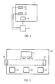
- the apparatus of the present invention comprises a bonding module 1 and a load lock module 2. Bonding is performed in a vacuum chamber of the bonding module 1.
- the vacuum in the vacuum chamber of the bonding module 1 is established by a vacuum pumping means 3 that is connected to the vacuum chamber of the bonding module 1 via a control valve 4.
- a vacuum can be provided in the load lock module 2 by another vacuum pumping means 5 that is connected by another control valve 6 to the load lock module 2.
- a single vacuum pumping means is connected by separate control valves to both the load lock module and the bonding module.
- the load lock module 2 comprises a first gate 7 that is opened when a wafer is transferred from the load lock module 2 to the bonding module 1 and a second gate 8 that is opened when a wafer is transferred by a robot to the load lock module 2.
- the load lock module 2 may be configured as a one-wafer transfer module providing one single wafer at the same time to the bonding module 1 or may include a multi wafer storing systems for receiving multiple wafers via the second gate 8 and storing the same and, then, providing these multiple wafers to the bonding module 1 at the same time.
- the load lock module 2 is evacuated to some predetermined pressure. Evacuation may be provided by the pumping device 5 at a rate of between 2.5 and 1,000 m 3 /h, in particular, more than 500 m 3 /h.
- the load lock module 2 is evacuated for example, to a pressure of about 1 mbars to some hundred mbar or to below atmospheric pressure.
- the vacuum chamber of the bonding module 1 is, for example, evacuated to a pressure in the range of 0.01 mbars to 10 mbars or 100mbars, in particular, 0.1 mbars to 5 mbars.
- the one or more wafers are transferred upon opening of the first gate 7 to the vacuum chamber of the bonding module 1 that was already evacuated by the first pumping means 3. Since during this transfer of the one or more wafers from the load lock module 2 to the bonding module 1 the latter is not exposed to atmospheric pressure only relatively slight adjustment of the pressure of the vacuum chamber of the bonding module 1 is necessary (if at all) after completion of the wafer transfer and closing the first gate 7. Thus, the throughput can significantly be increased.
- the throughput can be even further increased when another load lock module is provided, for example, on the left-hand-side of the bonding module 1 of Figure 1 and connected to the bonding module 1 to receive the already bonded wafers.
- the other load lock module shall also be evacuated before transfer of the bonded wafers from the bonding module 1.
- the load lock module 1 can be used to output the bonded wafers from the bonding module 1 to the external environment.
- the bonding module comprises a vacuum chamber and is connected to a pumping device as described with reference to Figure 1 .
- the bonding module comprises an optical system 9 that allows determining the exact position of alignment marks on the surfaces of the wafers to be bonded in the bonding module 1.
- the optical system 9 is only necessary if the two wafers need to be perfectly aligned with micrometer precision. This is the case when the two wafers present micro components.
- micro components elements are designated that result from technical steps carried out on or in the layers that must be positioned with precision.
- the micro components may be active or passive components, a mere contact point, or interconnections, like surface copper contact and interconnects.
- the alignment step may and thus provision of the optical system 9 are not necessary.
- the bonding module 1 is provided with a first bonding chuck 10 and a second bonding chuck 11 that clamp a first wafer 12 and a second wafer 13, respectively.
- the bonding chucks 10 and 11 may be made of metal or ceramics to maintain planarity of the wafers 12 and 13. Whereas in Figure 2 the bonding chucks 11 and 12 are shown to hold the wafers 12 and 13 horizontally, the bonding chucks 11 and 12 may advantageously be arranged to hold the wafers 12 and 13 vertically. In this case, deformation of the wafers due to their own weight can be avoided.
- the optical system 9 is electrically coupled to a control unit 14 that is computing the displacement of the bonding chucks 11 and 12 (in the plane and in rotation) in order to perfectly align the two wafers 12 and 13. Moreover, the control unit 14 controls movement of the of the bonding chucks 11 and 12 to each other until the wafers 12 and 13 come into contact for molecular bonding.
- Figure 3 illustrates an example of a manufacturing system 20 comprising the apparatus illustrated in Figure 1 .
- the manufacturing system 20 comprises a bonding module 1, for example, the bonding module 1 shown in Figure 2 , and two load lock modules 2 and 2'.
- the manufacturing system 20 includes at least a load port 21 for introducing wafers into the manufacturing system 20.
- a robot 22 is configured to manipulate and transfer the wafers from the load port 21 to any individual module of the manufacturing system 20, and also from one module to the other.
- the robot is moving along a robot moving area (indicated by dashed lines), to enable the transfer of the wafer from one place to another.
- the manufacturing system 20 comprises a plasma station 23 for activating one or two main surfaces of the wafers introduced into the manufacturing system 20.
- a second plasma station could be added, if the wafer processing requires that the main surface of both wafers to be bonded need to be activated.
- the same plasma station 23 can be used to treat surfaces to be bonded of each respective wafer.
- a first cleaning station 24 is provided to clean a bonding main surface of a first wafer and a second cleaning station 25 is provided to clean a bonding main surface of a second wafer.
- the manufacturing system 20 further comprises a control unit (not shown in Figure 3 ) for controlling the robot means 22 for transporting wafers in the manufacturing system 20.
- the control unit may control the robot means 22 to:
Landscapes
- Container, Conveyance, Adherence, Positioning, Of Wafer (AREA)
- Pressure Welding/Diffusion-Bonding (AREA)
- Engineering & Computer Science (AREA)
- Manufacturing & Machinery (AREA)
Priority Applications (1)
| Application Number | Priority Date | Filing Date | Title |
|---|---|---|---|
| EP11009599.9A EP2432007A3 (de) | 2010-06-22 | 2011-06-20 | Vorrichtung zur Herstellung von Halbleiterbauelementen |
Applications Claiming Priority (1)
| Application Number | Priority Date | Filing Date | Title |
|---|---|---|---|
| FR1002618A FR2961630B1 (fr) | 2010-06-22 | 2010-06-22 | Appareil de fabrication de dispositifs semi-conducteurs |
Related Child Applications (2)
| Application Number | Title | Priority Date | Filing Date |
|---|---|---|---|
| EP11009599.9A Division EP2432007A3 (de) | 2010-06-22 | 2011-06-20 | Vorrichtung zur Herstellung von Halbleiterbauelementen |
| EP11009599.9 Division-Into | 2011-12-05 |
Publications (2)
| Publication Number | Publication Date |
|---|---|
| EP2400526A2 true EP2400526A2 (de) | 2011-12-28 |
| EP2400526A3 EP2400526A3 (de) | 2013-01-16 |
Family
ID=42699871
Family Applications (2)
| Application Number | Title | Priority Date | Filing Date |
|---|---|---|---|
| EP20110005013 Withdrawn EP2400526A3 (de) | 2010-06-22 | 2011-06-20 | Vorrichtung zur herstellung von halbleitervorrichtungen |
| EP11009599.9A Withdrawn EP2432007A3 (de) | 2010-06-22 | 2011-06-20 | Vorrichtung zur Herstellung von Halbleiterbauelementen |
Family Applications After (1)
| Application Number | Title | Priority Date | Filing Date |
|---|---|---|---|
| EP11009599.9A Withdrawn EP2432007A3 (de) | 2010-06-22 | 2011-06-20 | Vorrichtung zur Herstellung von Halbleiterbauelementen |
Country Status (8)
| Country | Link |
|---|---|
| US (4) | US20110308721A1 (de) |
| EP (2) | EP2400526A3 (de) |
| JP (2) | JP5943408B2 (de) |
| KR (2) | KR101234001B1 (de) |
| CN (3) | CN105428285A (de) |
| FR (1) | FR2961630B1 (de) |
| SG (1) | SG177106A1 (de) |
| TW (2) | TWI449118B (de) |
Families Citing this family (17)
| Publication number | Priority date | Publication date | Assignee | Title |
|---|---|---|---|---|
| JP3314788B2 (ja) | 1993-04-27 | 2002-08-12 | 戸田工業株式会社 | 粒状マグネタイト粒子粉末及びその製造法 |
| FR2935536B1 (fr) * | 2008-09-02 | 2010-09-24 | Soitec Silicon On Insulator | Procede de detourage progressif |
| FR2961630B1 (fr) | 2010-06-22 | 2013-03-29 | Soitec Silicon On Insulator Technologies | Appareil de fabrication de dispositifs semi-conducteurs |
| US8338266B2 (en) | 2010-08-11 | 2012-12-25 | Soitec | Method for molecular adhesion bonding at low pressure |
| FR2964193A1 (fr) | 2010-08-24 | 2012-03-02 | Soitec Silicon On Insulator | Procede de mesure d'une energie d'adhesion, et substrats associes |
| DE102010048043A1 (de) * | 2010-10-15 | 2012-04-19 | Ev Group Gmbh | Vorrichtung und Verfahren zur Prozessierung von Wafern |
| US8844793B2 (en) * | 2010-11-05 | 2014-09-30 | Raytheon Company | Reducing formation of oxide on solder |
| JP6011034B2 (ja) * | 2012-06-04 | 2016-10-19 | 株式会社村田製作所 | ウエハ接合装置 |
| CN103489805A (zh) * | 2012-06-12 | 2014-01-01 | 苏州美图半导体技术有限公司 | 晶圆键合系统 |
| JP5977592B2 (ja) | 2012-06-20 | 2016-08-24 | 東京応化工業株式会社 | 貼付装置 |
| CN103626122B (zh) * | 2013-04-28 | 2016-05-11 | 苏州迪纳精密设备有限公司 | 一种阳极键合批量化生产设备 |
| US20170207191A1 (en) * | 2016-01-15 | 2017-07-20 | Taiwan Semiconductor Manufacturing Company Ltd. | Bonding system and associated apparatus and method |
| EP3382744A1 (de) | 2016-02-16 | 2018-10-03 | EV Group E. Thallner GmbH | Vorrichtung zum bonden von substraten |
| CN105904824B (zh) * | 2016-04-22 | 2017-09-29 | 哈尔滨工业大学 | 一种利用水蒸气辅助及紫外光活化的被键合物键合装置及方法 |
| CN110120181A (zh) * | 2019-04-16 | 2019-08-13 | 武汉华星光电技术有限公司 | 加压脱泡装置及加压脱泡方法 |
| KR20230105177A (ko) * | 2022-01-03 | 2023-07-11 | 삼성전자주식회사 | 플라즈마 처리 장치, 이를 포함하는 기판 본딩 시스템 및 이를 이용한 기판 본딩 방법 |
| CN118712106B (zh) * | 2024-08-30 | 2024-11-26 | 海创智能装备(烟台)有限公司 | 一种晶圆键合系统及热压键合、直接键合和阳极键合方法 |
Citations (2)
| Publication number | Priority date | Publication date | Assignee | Title |
|---|---|---|---|---|
| CA2717076A1 (en) * | 2008-02-29 | 2009-09-03 | Takeshi Tsuno | Room temperature bonding apparatus |
| US20100122762A1 (en) | 2008-11-16 | 2010-05-20 | Suss Microtec Inc | Method and apparatus for wafer bonding with enhanced wafer mating |
Family Cites Families (81)
| Publication number | Priority date | Publication date | Assignee | Title |
|---|---|---|---|---|
| US10012A (en) * | 1853-09-13 | Safety-valve foe | ||
| IT1230026B (it) | 1988-10-28 | 1991-09-24 | Sgs Thomson Microelectronics | Processo di saldatura di fette di silicio fra loro, per la fabbricazione di dispositivi a semiconduttore |
| JPH0389519A (ja) | 1989-08-31 | 1991-04-15 | Sony Corp | 半導体基板の製法 |
| JPH0719737B2 (ja) | 1990-02-28 | 1995-03-06 | 信越半導体株式会社 | S01基板の製造方法 |
| JPH0636413B2 (ja) | 1990-03-29 | 1994-05-11 | 信越半導体株式会社 | 半導体素子形成用基板の製造方法 |
| JPH04263425A (ja) | 1991-02-18 | 1992-09-18 | Toshiba Corp | 半導体基板の研削装置及び研削方法 |
| JP3132029B2 (ja) * | 1991-03-18 | 2001-02-05 | ソニー株式会社 | ウエハ貼り合わせ装置 |
| US5223001A (en) * | 1991-11-21 | 1993-06-29 | Tokyo Electron Kabushiki Kaisha | Vacuum processing apparatus |
| KR0126455B1 (ko) | 1992-05-18 | 1997-12-24 | 가나이 쯔또무 | 수지재료의 접착강도 측정방법 |
| JP2701709B2 (ja) * | 1993-02-16 | 1998-01-21 | 株式会社デンソー | 2つの材料の直接接合方法及び材料直接接合装置 |
| JP3321882B2 (ja) | 1993-02-28 | 2002-09-09 | ソニー株式会社 | 基板はり合わせ方法 |
| JPH0799295A (ja) | 1993-06-07 | 1995-04-11 | Canon Inc | 半導体基体の作成方法及び半導体基体 |
| JP2662495B2 (ja) | 1993-06-28 | 1997-10-15 | 住友シチックス株式会社 | 接着半導体基板の製造方法 |
| US5696327A (en) | 1994-11-23 | 1997-12-09 | Regents Of The University Of Minnesota | Method and apparatus for separating a thin film from a substrate |
| US5668045A (en) | 1994-11-30 | 1997-09-16 | Sibond, L.L.C. | Process for stripping outer edge of BESOI wafers |
| US6113721A (en) | 1995-01-03 | 2000-09-05 | Motorola, Inc. | Method of bonding a semiconductor wafer |
| US5937312A (en) | 1995-03-23 | 1999-08-10 | Sibond L.L.C. | Single-etch stop process for the manufacture of silicon-on-insulator wafers |
| JPH0917984A (ja) | 1995-06-29 | 1997-01-17 | Sumitomo Sitix Corp | 貼り合わせsoi基板の製造方法 |
| JP3352896B2 (ja) | 1997-01-17 | 2002-12-03 | 信越半導体株式会社 | 貼り合わせ基板の作製方法 |
| JP3352902B2 (ja) | 1997-02-21 | 2002-12-03 | 信越半導体株式会社 | 貼り合わせ基板の作製方法 |
| JP3720515B2 (ja) | 1997-03-13 | 2005-11-30 | キヤノン株式会社 | 基板処理装置及びその方法並びに基板の製造方法 |
| JP3132425B2 (ja) | 1997-06-20 | 2001-02-05 | 日本電気株式会社 | 衛星イントラネットサービスにおける通信時間短縮方式 |
| JP2001511608A (ja) * | 1997-07-29 | 2001-08-14 | シリコン ジェネシス コーポレイション | プラズマ侵入型イオン注入を使用するクラスタツール方法及び装置 |
| JP3216583B2 (ja) | 1997-08-22 | 2001-10-09 | 住友金属工業株式会社 | 貼り合わせsoi基板の製造方法 |
| EP1018153A1 (de) | 1997-08-29 | 2000-07-12 | Sharon N. Farrens | In sito-plasmaverbindungsverfahren für scheiben |
| EP0935280B1 (de) | 1998-02-04 | 2004-06-09 | Canon Kabushiki Kaisha | SOI Substrat |
| US6221774B1 (en) | 1998-04-10 | 2001-04-24 | Silicon Genesis Corporation | Method for surface treatment of substrates |
| US6117695A (en) | 1998-05-08 | 2000-09-12 | Lsi Logic Corporation | Apparatus and method for testing a flip chip integrated circuit package adhesive layer |
| US6008113A (en) * | 1998-05-19 | 1999-12-28 | Kavlico Corporation | Process for wafer bonding in a vacuum |
| JP3635200B2 (ja) | 1998-06-04 | 2005-04-06 | 信越半導体株式会社 | Soiウェーハの製造方法 |
| JPH11354761A (ja) | 1998-06-09 | 1999-12-24 | Sumitomo Metal Ind Ltd | Soi基板及びその製造方法 |
| JP3321455B2 (ja) | 1999-04-02 | 2002-09-03 | 株式会社アークテック | 電極引張試験方法、その装置及び電極引張試験用の基板/プローブ支持装置並びに電極プローブ接合装置 |
| US20020187595A1 (en) | 1999-08-04 | 2002-12-12 | Silicon Evolution, Inc. | Methods for silicon-on-insulator (SOI) manufacturing with improved control and site thickness variations and improved bonding interface quality |
| JP3632531B2 (ja) | 1999-11-17 | 2005-03-23 | 株式会社デンソー | 半導体基板の製造方法 |
| US6616332B1 (en) | 1999-11-18 | 2003-09-09 | Sensarray Corporation | Optical techniques for measuring parameters such as temperature across a surface |
| KR100789205B1 (ko) | 2000-03-29 | 2007-12-31 | 신에쯔 한도타이 가부시키가이샤 | 실리콘 웨이퍼 및 에스오아이 웨이퍼의 제조방법, 그리고그 에스오아이 웨이퍼 |
| JP4822577B2 (ja) * | 2000-08-18 | 2011-11-24 | 東レエンジニアリング株式会社 | 実装方法および装置 |
| CN1315615C (zh) * | 2000-09-27 | 2007-05-16 | 斯特拉斯保 | 用于设置弹性带的工具及相关方法 |
| WO2003008938A2 (de) | 2001-07-16 | 2003-01-30 | Siemens Aktiengesellschaft | Verfahren zum bestimmen der haftfestigkeit einer beschichtung auf einem bauteil |
| US6736017B2 (en) | 2001-08-24 | 2004-05-18 | Symyx Technologies, Inc. | High throughput mechanical rapid serial property testing of materials libraries |
| JP2003115519A (ja) * | 2001-10-04 | 2003-04-18 | Mitsubishi Electric Corp | 半導体装置の製造方法、半導体製造装置、ロードロック室、基板収納ケース、ストッカ |
| JP4093793B2 (ja) | 2002-04-30 | 2008-06-04 | 信越半導体株式会社 | 半導体ウエーハの製造方法及びウエーハ |
| FR2874455B1 (fr) | 2004-08-19 | 2008-02-08 | Soitec Silicon On Insulator | Traitement thermique avant collage de deux plaquettes |
| US6846380B2 (en) * | 2002-06-13 | 2005-01-25 | The Boc Group, Inc. | Substrate processing apparatus and related systems and methods |
| US6958255B2 (en) | 2002-08-08 | 2005-10-25 | The Board Of Trustees Of The Leland Stanford Junior University | Micromachined ultrasonic transducers and method of fabrication |
| JP4556158B2 (ja) | 2002-10-22 | 2010-10-06 | 株式会社Sumco | 貼り合わせsoi基板の製造方法および半導体装置 |
| US6790748B2 (en) | 2002-12-19 | 2004-09-14 | Intel Corporation | Thinning techniques for wafer-to-wafer vertical stacks |
| US7176528B2 (en) | 2003-02-18 | 2007-02-13 | Corning Incorporated | Glass-based SOI structures |
| US7399681B2 (en) | 2003-02-18 | 2008-07-15 | Corning Incorporated | Glass-based SOI structures |
| JP4066889B2 (ja) | 2003-06-09 | 2008-03-26 | 株式会社Sumco | 貼り合わせ基板およびその製造方法 |
| JPWO2005022610A1 (ja) | 2003-09-01 | 2007-11-01 | 株式会社Sumco | 貼り合わせウェーハの製造方法 |
| WO2005034233A1 (en) * | 2003-10-09 | 2005-04-14 | Snt Co., Ltd | Electro-static chuck with non-sintered aln and a method of preparing the same |
| FR2860842B1 (fr) | 2003-10-14 | 2007-11-02 | Tracit Technologies | Procede de preparation et d'assemblage de substrats |
| JP4744855B2 (ja) * | 2003-12-26 | 2011-08-10 | 日本碍子株式会社 | 静電チャック |
| KR101026956B1 (ko) | 2004-03-05 | 2011-04-11 | 더 리전트 오브 더 유니버시티 오브 캘리포니아 | 극박 필름의 분리를 위한 유리-변형 응력파 및나노일렉트로닉스 장치 제작 |
| JP4821091B2 (ja) * | 2004-04-08 | 2011-11-24 | 株式会社ニコン | ウェハの接合装置 |
| US7442992B2 (en) | 2004-05-19 | 2008-10-28 | Sumco Corporation | Bonded SOI substrate, and method for manufacturing the same |
| EP1815500A2 (de) * | 2004-10-09 | 2007-08-08 | Applied Microengineering Limited | Geräte zur wafer-bondierung |
| JP2006303087A (ja) | 2005-04-19 | 2006-11-02 | Sumco Corp | シリコンウェーハの貼り合わせ方法および貼り合わせ装置 |
| JP4918229B2 (ja) | 2005-05-31 | 2012-04-18 | 信越半導体株式会社 | 貼り合わせウエーハの製造方法 |
| JP5122731B2 (ja) | 2005-06-01 | 2013-01-16 | 信越半導体株式会社 | 貼り合わせウェーハの製造方法 |
| JP4107316B2 (ja) * | 2005-09-02 | 2008-06-25 | 株式会社日立プラントテクノロジー | 基板貼合装置 |
| US7705342B2 (en) | 2005-09-16 | 2010-04-27 | University Of Cincinnati | Porous semiconductor-based evaporator having porous and non-porous regions, the porous regions having through-holes |
| KR100755368B1 (ko) | 2006-01-10 | 2007-09-04 | 삼성전자주식회사 | 3차원 구조를 갖는 반도체 소자의 제조 방법들 및 그에의해 제조된 반도체 소자들 |
| JP4721435B2 (ja) | 2006-04-06 | 2011-07-13 | 本田技研工業株式会社 | 接着部の剥離検査方法 |
| TWI363212B (en) * | 2006-05-26 | 2012-05-01 | Advanced Display Proc Eng Co | Adhesive chuck, and apparatus and method for assembling substrates using the same |
| CN101090082A (zh) * | 2006-06-15 | 2007-12-19 | 中国科学院半导体研究所 | 多功能半导体晶片键合装置 |
| US20080044984A1 (en) | 2006-08-16 | 2008-02-21 | Taiwan Semiconductor Manufacturing Co., Ltd. | Methods of avoiding wafer breakage during manufacture of backside illuminated image sensors |
| US7473909B2 (en) | 2006-12-04 | 2009-01-06 | Axcelis Technologies, Inc. | Use of ion induced luminescence (IIL) as feedback control for ion implantation |
| WO2008069259A1 (en) * | 2006-12-05 | 2008-06-12 | Semiconductor Energy Laboratory Co., Ltd. | Film formation apparatus, film formation method, manufacturing apparatus, and method for manufacturing light-emitting device |
| FR2912839B1 (fr) | 2007-02-16 | 2009-05-15 | Soitec Silicon On Insulator | Amelioration de la qualite de l'interface de collage par nettoyage froid et collage a chaud |
| JP5143477B2 (ja) | 2007-05-31 | 2013-02-13 | 信越化学工業株式会社 | Soiウエーハの製造方法 |
| US8245751B2 (en) * | 2007-11-07 | 2012-08-21 | Advanced Display Process Engineering Co., Ltd. | Substrate bonding apparatus |
| JP5320736B2 (ja) * | 2007-12-28 | 2013-10-23 | 株式会社ニコン | 半導体ウエハ貼り合わせ装置 |
| FR2935537B1 (fr) | 2008-08-28 | 2010-10-22 | Soitec Silicon On Insulator | Procede d'initiation d'adhesion moleculaire |
| FR2935536B1 (fr) | 2008-09-02 | 2010-09-24 | Soitec Silicon On Insulator | Procede de detourage progressif |
| FR2935535B1 (fr) | 2008-09-02 | 2010-12-10 | S O I Tec Silicon On Insulator Tech | Procede de detourage mixte. |
| EP2200077B1 (de) | 2008-12-22 | 2012-12-05 | Soitec | Verfahren zur Bindung zweier Substrate |
| FR2961630B1 (fr) | 2010-06-22 | 2013-03-29 | Soitec Silicon On Insulator Technologies | Appareil de fabrication de dispositifs semi-conducteurs |
| US8338266B2 (en) | 2010-08-11 | 2012-12-25 | Soitec | Method for molecular adhesion bonding at low pressure |
| FR2964193A1 (fr) | 2010-08-24 | 2012-03-02 | Soitec Silicon On Insulator | Procede de mesure d'une energie d'adhesion, et substrats associes |
-
2010
- 2010-06-22 FR FR1002618A patent/FR2961630B1/fr not_active Expired - Fee Related
- 2010-09-22 US US12/888,251 patent/US20110308721A1/en not_active Abandoned
-
2011
- 2011-06-17 TW TW100145647A patent/TWI449118B/zh not_active IP Right Cessation
- 2011-06-17 TW TW100121311A patent/TWI443769B/zh not_active IP Right Cessation
- 2011-06-20 EP EP20110005013 patent/EP2400526A3/de not_active Withdrawn
- 2011-06-20 JP JP2011136614A patent/JP5943408B2/ja not_active Expired - Fee Related
- 2011-06-20 EP EP11009599.9A patent/EP2432007A3/de not_active Withdrawn
- 2011-06-21 CN CN201610052078.7A patent/CN105428285A/zh active Pending
- 2011-06-21 SG SG2011045515A patent/SG177106A1/en unknown
- 2011-06-21 CN CN2011102122527A patent/CN102299048A/zh active Pending
- 2011-06-21 CN CN201110414307.2A patent/CN102437073B/zh not_active Expired - Fee Related
- 2011-06-21 KR KR20110060332A patent/KR101234001B1/ko not_active Expired - Fee Related
- 2011-11-29 US US13/306,719 patent/US20120067524A1/en not_active Abandoned
- 2011-12-26 JP JP2011283992A patent/JP5776538B2/ja not_active Expired - Fee Related
-
2012
- 2012-01-05 KR KR1020120001471A patent/KR101363351B1/ko not_active Expired - Fee Related
- 2012-09-21 US US13/624,470 patent/US9138980B2/en active Active
-
2015
- 2015-05-27 US US14/722,794 patent/US20150279830A1/en not_active Abandoned
Patent Citations (2)
| Publication number | Priority date | Publication date | Assignee | Title |
|---|---|---|---|---|
| CA2717076A1 (en) * | 2008-02-29 | 2009-09-03 | Takeshi Tsuno | Room temperature bonding apparatus |
| US20100122762A1 (en) | 2008-11-16 | 2010-05-20 | Suss Microtec Inc | Method and apparatus for wafer bonding with enhanced wafer mating |
Non-Patent Citations (1)
| Title |
|---|
| BURNS ET AL.: "A Wafer-Scale 3-D Circuit Integration Technology", IEEE TRANSACTIONS ON ELECTRON DEVICES, vol. 53, no. 10, October 2006 (2006-10-01), pages 2507 - 2516 |
Also Published As
| Publication number | Publication date |
|---|---|
| US20150279830A1 (en) | 2015-10-01 |
| KR20110139149A (ko) | 2011-12-28 |
| JP2012099839A (ja) | 2012-05-24 |
| FR2961630A1 (fr) | 2011-12-23 |
| TWI443769B (zh) | 2014-07-01 |
| EP2432007A3 (de) | 2017-03-22 |
| US20120067524A1 (en) | 2012-03-22 |
| JP5943408B2 (ja) | 2016-07-05 |
| TW201225203A (en) | 2012-06-16 |
| US9138980B2 (en) | 2015-09-22 |
| TW201203438A (en) | 2012-01-16 |
| KR101363351B1 (ko) | 2014-02-14 |
| CN102437073B (zh) | 2015-07-22 |
| TWI449118B (zh) | 2014-08-11 |
| JP5776538B2 (ja) | 2015-09-09 |
| CN102299048A (zh) | 2011-12-28 |
| EP2400526A3 (de) | 2013-01-16 |
| JP2012039089A (ja) | 2012-02-23 |
| US20110308721A1 (en) | 2011-12-22 |
| EP2432007A2 (de) | 2012-03-21 |
| US20130032272A1 (en) | 2013-02-07 |
| FR2961630B1 (fr) | 2013-03-29 |
| KR20120016299A (ko) | 2012-02-23 |
| CN102437073A (zh) | 2012-05-02 |
| SG177106A1 (en) | 2012-01-30 |
| KR101234001B1 (ko) | 2013-02-18 |
| CN105428285A (zh) | 2016-03-23 |
Similar Documents
| Publication | Publication Date | Title |
|---|---|---|
| EP2400526A2 (de) | Vorrichtung zur herstellung von halbleitervorrichtungen | |
| TWI735895B (zh) | 共價接合之半導體界面 | |
| US7645681B2 (en) | Bonding method, device produced by this method, and bonding device | |
| US12062521B2 (en) | Method for prefixing of substrates | |
| KR20160018410A (ko) | 접합 장치, 접합 시스템, 접합 방법 및 컴퓨터 기억 매체 | |
| JP6014302B2 (ja) | 貼り合わせ装置および貼り合わせ方法 | |
| KR102404840B1 (ko) | 반송 방법 및 첩부 장치 | |
| JP2017034107A (ja) | 接合装置、接合システム、接合方法、プログラム及びコンピュータ記憶媒体 | |
| JP3820409B2 (ja) | 接合方法及びこの方法により作成されるデバイス並びに接合装置 | |
| JP2006248895A (ja) | 接合方法及びこの方法により作成されるデバイス並びに接合装置 | |
| JP6244188B2 (ja) | 接合装置、接合方法および接合システム | |
| CN219873412U (zh) | 一种晶圆键合设备 | |
| Suga et al. | A new wafer-bonder of ultra-high precision using surface activated bonding (SAB) concept | |
| US20260052945A1 (en) | Substrate-to-substrate bonding using electrostatic chucks | |
| KR20260010981A (ko) | 기판 본딩 장치, 이를 포함하는 기판 본딩 시스템 및 기판 본딩 방법 | |
| JP2011129777A (ja) | 基板重ね合わせ装置及びデバイスの製造方法 |
Legal Events
| Date | Code | Title | Description |
|---|---|---|---|
| AK | Designated contracting states |
Kind code of ref document: A2 Designated state(s): AL AT BE BG CH CY CZ DE DK EE ES FI FR GB GR HR HU IE IS IT LI LT LU LV MC MK MT NL NO PL PT RO RS SE SI SK SM TR |
|
| AX | Request for extension of the european patent |
Extension state: BA ME |
|
| PUAI | Public reference made under article 153(3) epc to a published international application that has entered the european phase |
Free format text: ORIGINAL CODE: 0009012 |
|
| RAP1 | Party data changed (applicant data changed or rights of an application transferred) |
Owner name: SOITEC |
|
| PUAL | Search report despatched |
Free format text: ORIGINAL CODE: 0009013 |
|
| AK | Designated contracting states |
Kind code of ref document: A3 Designated state(s): AL AT BE BG CH CY CZ DE DK EE ES FI FR GB GR HR HU IE IS IT LI LT LU LV MC MK MT NL NO PL PT RO RS SE SI SK SM TR |
|
| RIC1 | Information provided on ipc code assigned before grant |
Ipc: H01L 21/67 20060101AFI20121212BHEP |
|
| 17P | Request for examination filed |
Effective date: 20130416 |
|
| 17Q | First examination report despatched |
Effective date: 20160524 |
|
| STAA | Information on the status of an ep patent application or granted ep patent |
Free format text: STATUS: THE APPLICATION IS DEEMED TO BE WITHDRAWN |
|
| 18D | Application deemed to be withdrawn |
Effective date: 20161005 |