EP2365415B1 - Mobiles Endgerät und Verfahren zur Abstrahlung dessen Wärme - Google Patents
Mobiles Endgerät und Verfahren zur Abstrahlung dessen Wärme Download PDFInfo
- Publication number
- EP2365415B1 EP2365415B1 EP11004735A EP11004735A EP2365415B1 EP 2365415 B1 EP2365415 B1 EP 2365415B1 EP 11004735 A EP11004735 A EP 11004735A EP 11004735 A EP11004735 A EP 11004735A EP 2365415 B1 EP2365415 B1 EP 2365415B1
- Authority
- EP
- European Patent Office
- Prior art keywords
- circuit board
- heat
- heat conduction
- conduction layer
- mobile terminal
- Prior art date
- Legal status (The legal status is an assumption and is not a legal conclusion. Google has not performed a legal analysis and makes no representation as to the accuracy of the status listed.)
- Expired - Lifetime
Links
Images


Classifications
-
- H—ELECTRICITY
- H05—ELECTRIC TECHNIQUES NOT OTHERWISE PROVIDED FOR
- H05K—PRINTED CIRCUITS; CASINGS OR CONSTRUCTIONAL DETAILS OF ELECTRIC APPARATUS; MANUFACTURE OF ASSEMBLAGES OF ELECTRICAL COMPONENTS
- H05K1/00—Printed circuits
- H05K1/02—Details
- H05K1/0201—Thermal arrangements, e.g. for cooling, heating or preventing overheating
- H05K1/0203—Cooling of mounted components
- H05K1/0207—Cooling of mounted components using internal conductor planes parallel to the surface for thermal conduction, e.g. power planes
-
- G—PHYSICS
- G06—COMPUTING OR CALCULATING; COUNTING
- G06F—ELECTRIC DIGITAL DATA PROCESSING
- G06F1/00—Details not covered by groups G06F3/00 - G06F13/00 and G06F21/00
- G06F1/16—Constructional details or arrangements
- G06F1/20—Cooling means
- G06F1/203—Cooling means for portable computers, e.g. for laptops
-
- H—ELECTRICITY
- H04—ELECTRIC COMMUNICATION TECHNIQUE
- H04M—TELEPHONIC COMMUNICATION
- H04M1/00—Substation equipment, e.g. for use by subscribers
- H04M1/02—Constructional features of telephone sets
- H04M1/0202—Portable telephone sets, e.g. cordless phones, mobile phones or bar type handsets
-
- H—ELECTRICITY
- H05—ELECTRIC TECHNIQUES NOT OTHERWISE PROVIDED FOR
- H05K—PRINTED CIRCUITS; CASINGS OR CONSTRUCTIONAL DETAILS OF ELECTRIC APPARATUS; MANUFACTURE OF ASSEMBLAGES OF ELECTRICAL COMPONENTS
- H05K1/00—Printed circuits
- H05K1/02—Details
- H05K1/0201—Thermal arrangements, e.g. for cooling, heating or preventing overheating
- H05K1/0203—Cooling of mounted components
- H05K1/0204—Cooling of mounted components using means for thermal conduction connection in the thickness direction of the substrate
- H05K1/0206—Cooling of mounted components using means for thermal conduction connection in the thickness direction of the substrate by printed thermal vias
-
- H—ELECTRICITY
- H05—ELECTRIC TECHNIQUES NOT OTHERWISE PROVIDED FOR
- H05K—PRINTED CIRCUITS; CASINGS OR CONSTRUCTIONAL DETAILS OF ELECTRIC APPARATUS; MANUFACTURE OF ASSEMBLAGES OF ELECTRICAL COMPONENTS
- H05K1/00—Printed circuits
- H05K1/02—Details
- H05K1/03—Use of materials for the substrate
- H05K1/05—Insulated conductive substrates, e.g. insulated metal substrate
- H05K1/056—Insulated conductive substrates, e.g. insulated metal substrate the metal substrate being covered by an organic insulating layer
-
- H—ELECTRICITY
- H05—ELECTRIC TECHNIQUES NOT OTHERWISE PROVIDED FOR
- H05K—PRINTED CIRCUITS; CASINGS OR CONSTRUCTIONAL DETAILS OF ELECTRIC APPARATUS; MANUFACTURE OF ASSEMBLAGES OF ELECTRICAL COMPONENTS
- H05K1/00—Printed circuits
- H05K1/02—Details
- H05K1/14—Structural association of two or more printed circuits
- H05K1/141—One or more single auxiliary printed circuits mounted on a main printed circuit, e.g. modules, adapters
-
- H—ELECTRICITY
- H05—ELECTRIC TECHNIQUES NOT OTHERWISE PROVIDED FOR
- H05K—PRINTED CIRCUITS; CASINGS OR CONSTRUCTIONAL DETAILS OF ELECTRIC APPARATUS; MANUFACTURE OF ASSEMBLAGES OF ELECTRICAL COMPONENTS
- H05K1/00—Printed circuits
- H05K1/02—Details
- H05K1/14—Structural association of two or more printed circuits
- H05K1/148—Arrangements of two or more hingeably connected rigid printed circuit boards, i.e. connected by flexible means
-
- H—ELECTRICITY
- H05—ELECTRIC TECHNIQUES NOT OTHERWISE PROVIDED FOR
- H05K—PRINTED CIRCUITS; CASINGS OR CONSTRUCTIONAL DETAILS OF ELECTRIC APPARATUS; MANUFACTURE OF ASSEMBLAGES OF ELECTRICAL COMPONENTS
- H05K2201/00—Indexing scheme relating to printed circuits covered by H05K1/00
- H05K2201/06—Thermal details
- H05K2201/062—Means for thermal insulation, e.g. for protection of parts
-
- H—ELECTRICITY
- H05—ELECTRIC TECHNIQUES NOT OTHERWISE PROVIDED FOR
- H05K—PRINTED CIRCUITS; CASINGS OR CONSTRUCTIONAL DETAILS OF ELECTRIC APPARATUS; MANUFACTURE OF ASSEMBLAGES OF ELECTRICAL COMPONENTS
- H05K3/00—Apparatus or processes for manufacturing printed circuits
- H05K3/46—Manufacturing multilayer circuits
- H05K3/4611—Manufacturing multilayer circuits by laminating two or more circuit boards
- H05K3/4641—Manufacturing multilayer circuits by laminating two or more circuit boards having integrally laminated metal sheets or special power cores
Definitions
- the present invention relates to a mobile terminal device and a method for radiating heat therefrom, more particularly, to a structure of a circuit board in a mobile terminal device, on which heat-generating components are mounted, and to a method for radiating heat using the circuit board.
- Mobile terminal devices as typified by mobile phones are provided with various functions, such as a video phone function, a photographing function and a TV broadcast receiving function, in addition to a voice communications function and a mail sending/receiving function.
- a video phone function such as a digital camera
- a photographing function such as a digital camera
- a TV broadcast receiving function such as a digital broadcast station
- a voice communications function such as a facsiver, a facsonic mail, or a mail sending/receiving function.
- a mail sending/receiving function For the purpose of realizing these functions, efforts have been made to improve the processing capacities of mobile terminal devices.
- As mobile terminal devices are made high in function and performance, the power consumed in the electronic components mounted inside the mobile terminal devices increases. As a result, the temperature rises in the mobile terminal devices have lead to problems.
- mobile terminal devices are also required to be reduced in thickness, the clearance between the electronic components and the housing cannot be increased, and the heat generated in the electronic components is transferred immediately to the surface of the housing. As a result, a problem of local temperature rising at the surface of the housing result.
- US 2004/0041256 A1 is directed to a high-frequency amplifier circuit device for use in portable devices.
- the circuit device comprises a printed circuit board and a heat conduction layer. Heat generated at a power element of the circuit device is conducted via the heat conduction layer, heat dissipation vias and an electrode to a copper pattern of the printed circuit board.
- An object of the present invention is to provide a mobile terminal device capable of suppressing local temperature rising due to the heat generated in electronic components disposed inside and to provide a method for radiating the heat from the device.
- a mobile terminal device in accordance with the subject-matter of independent claim 1 is provided.
- a mobile terminal device comprises: a circuit board and heat-generating components mounted on the circuit board, characterized by further comprising at least one first heat conduction layer provided inside the circuit board, in which a member having a heat conductivity higher than that of the main constituent material of the circuit board is arranged in the direction of the face of the circuit board, wherein the heat generated in the heat-generating components is dispersed to the whole face of the circuit board via the heat conduction layer.
- the present invention can have a configuration wherein the heat-generating components are disposed on one face of the circuit board.
- the present invention can have a configuration further comprising a operation member on the face other than the face of the circuit board on which the heat-generating components are mounted, wherein at least one heat conduction suppressing layer having a heat conductivity lower than that of the main constituent material of the circuit board is provided inside the circuit board and between the first heat conduction layer and the operation member.
- the present invention can have a configuration wherein a connection member formed of a heat conduction member having a heat conductivity higher than that of the main constituent material of the circuit board and making contact with both of the first heat conduction layer and the heat-generating components is provided between the first heat conduction layer and the heat-generating components, and the first heat conduction layer is thermally connected to the heat-generating components by the connection member.
- the present invention can have a configuration wherein the heat-generating component is provided with a heat-radiating terminal that makes contact with the first heat conduction layer in a state that the heat-generating component is mounted, and the heat conduction layer is thermally connected to the heat-generating component by the heat-radiating terminal.
- the heat-radiating terminal is a terminal not contributing to the electrical connection of the heat-generating component and is preferably connected to the housing of the heat-generating component, or a circuit board or a component inside the heat-generating component.
- the heat-radiating terminal can be formed of a solder ball constituting BGA (Ball Grid Array).
- the present invention can have a configuration wherein the first heat conduction layer is formed on the whole face or part of the circuit board excluding the areas on which connection wires for connecting the front and back faces of the circuit board are formed as viewed in the normal direction of the circuit board.
- the present invention can also have a configuration wherein non-heat-resistant components are mounted on the circuit board, and the first heat conduction layer is formed on the whole face or part of the circuit board excluding the areas on which the no-heat-resistant components are mounted as viewed in the normal direction of the circuit board.
- the present invention can also have a configuration wherein the circuit board is fixed by protruding portions provided beforehand on the housing of the mobile terminal device, and the members of the circuit board between the first heat conduction layer and the protruding portions are removed in at least part of the areas corresponding to the protruding portions, and the heat conduction layer is thermally connected to at least part of the protruding portions.
- the present invention can also have a configuration wherein another circuit board is fixed to the circuit board, at least one second heat conduction layer in which a member having a heat conductivity higher than that of the main constituent material of the other circuit board is arranged in the direction of the face of the other circuit board is provided inside or on the surface of the other circuit board, the first heat conduction layer of the circuit board is thermally connected to the second heat conduction layer of the other circuit board by the connection member, and the heat generated in the heat-generating components mounted on the circuit board is transferred to the other circuit board via the connection member.
- the present invention can also have a configuration wherein the circuit board held in a first housing, an other circuit board held in a second housing and a connection circuit board for connecting the circuit board to the other circuit board are provided, at least one second heat conduction layer in which a member having a heat conductivity higher than that of the main constituent material of the other circuit board is provided in the direction of the face of the other circuit board is arranged inside or on the surface of the other circuit board, at least one third heat conduction layer in which a member having a heat conductivity higher than that of the main constituent material of the connection circuit board is arranged in the direction of the face of the connection circuit board is provided inside or on the surface of the connection circuit board, the first heat conduction layer of the circuit board is thermally connected to the third heat conduction layer of the connection circuit board by the connection member, and the third heat conduction layer of the connection circuit board is thermally connected to the second heat conduction layer of the other circuit board by the connection member, and the heat generated in the heat-generating components mounted on the circuit board is transferred to the other circuit
- the mobile terminal device is preferably a mobile phone, a mobile computer or a mobile game machine.
- a heat radiating method is a heat radiating method for a mobile terminal device equipped with a circuit board on which at least one heat-generating component is mounted, wherein at least one first heat conduction layer in which a member having a heat conductivity higher than that of the main constituent material of the circuit board is arranged in the direction of the face of the circuit board is provided inside the circuit board, and the heat generated in the heat-generating component is dispersed in the direction of the face of the circuit board by the heat conduction layer.
- the present invention further comprising the operation member on the face other than the face of the circuit board on which the heat-generating components are mounted can have a configuration wherein at least one heat conduction suppressing layer having a heat conductivity lower than that of the main constituent material of the circuit board is arranged inside the circuit board and between the first heat conduction layer and the operation member, and the transfer of the heat generated in the heat-generating components to the operation member is suppressed by the heat conduction suppressing layer.
- the present invention can also have a configuration wherein the first heat conduction layer is thermally connected to the heat-generating components by the connection member formed of a member having a heat conductivity higher than that of the main constituent material of the circuit board, and the heat generated in the heat-generating components is transferred to the first heat conduction layer via the connection member.
- the present invention can also have a configuration wherein protruding portions for fixing the circuit board are provided on the housing of the mobile terminal device, the members of the circuit board between the first heat conduction layer and the protruding portions are removed in at least part of the areas corresponding to the protruding portions so that the first heat conduction layer is thermally connected to the protruding portions, and the heat generated in the heat-generating components is transferred to the housing via the heat conduction layer and the protruding portions.
- the present invention can also have a configuration wherein at least one second heat conduction layer in which a member having a heat conductivity higher than that of the main constituent material of the other circuit board is provided in the direction of the face of the other circuit board is arranged inside or on the surface of the other circuit board fixed to the circuit board, the first heat conduction layer of the circuit board is thermally connected to the second heat conduction layer of the other circuit board by the connection member, and the heat generated in the heat-generating components mounted on the circuit board is transferred to the other circuit board via the connection member.
- the present invention comprising the circuit board held in the first housing, the other circuit board held in the second housing and the connection circuit board for connecting the circuit board to the other circuit board can also have a configuration wherein at least one second heat conduction layer in which a member having a heat conductivity higher than that of the main constituent material of the other circuit board is arranged in the direction of the face of the other circuit board is provided inside or on the surface of the other circuit board, at least one third heat conduction layer in which a member having a heat conductivity higher than that of the main constituent material of the connection circuit board is arranged in the direction of the face of the connection circuit board is provided inside or on the surface of the connection circuit board, the first heat conduction layer of the circuit board is thermally connected to the third heat conduction layer of the connection circuit board by the connection member, and the third heat conduction layer of the connection circuit board is thermally connected to the second heat conduction layer of the other circuit board by the connection member, and the heat generated in the heat-generating components mounted on the circuit board is transferred to the other circuit board via the connection
- the heat generated in the electronic components is dispersed in the direction of the face of the circuit board by at least one heat conduction layer arranged in the circuit board on which the electronic components are mounted, transferred from the whole face of the circuit board to the operation member, such as keys, and the whole of the housing, further transferred to the other circuit board connected to the circuit board and the components mounted on the other circuit board, and still further transferred to the other housing accommodating the other circuit board, and then radiated to the outside.
- the temperatures of the operation member and the housing do not rise locally, and heat radiation can be carried out efficiently.
- discomfort during operation due to local temperature rises can be relieved without significantly increasing the cost or the like and without increasing the thickness of the mobile terminal device.
- the mobile terminal device and the heat-radiating method according to the present invention have effects described below.
- a first effect of the present invention is that the local temperature rise at the operation member, such as keys, and the housing due to the heat generated in electronic components can be suppressed and that the temperature of the surface of the mobile terminal device can be made uniform.
- the reason is that the heat generated in the electronic components is dispersed in the direction of the face of the circuit board by at least one first heat conduction layer arranged in the circuit board on which the electronic components are mounted, transferred from the whole face of the circuit board to the operation member and the whole of the housing, further transferred to the other circuit board connected to the circuit board and the components mounted on the other circuit board, and still further transferred to the other housing accommodating the other circuit board, and then radiated to the outside.
- a second effect of the present invention is that the heat generated in the electronic components can be radiated effectively without significantly increasing the cost or the like and without increasing the thickness of the mobile terminal device.
- the reason is that the heat generated in the electronic components can be dispersed by a simple structure wherein heat conduction members are arranged in layers inside the circuit board and then radiated by the operation member and the whole of the housing, without installing heatsinks made of metal, fans or the like that are large in size.
- high-performance electronic components can be used by adopting this kind of heat-radiating structure.
- the rigidity of the circuit board can be raised by providing the heat transfer layer inside the circuit board. As a result, the deformation of the circuit board due to external forces encountered during dropping, key operation and the like can be suppressed, and the connection reliability of the electronic components can be improved.
- a structure wherein a heat conduction member is arranged inside the housing for example, Japanese Published Unexamined Patent Application No. 2002-323936
- a structure wherein a metal chassis is provided inside the housing for example, Japanese Published Unexamined Patent Application No. Hei 2-262724
- a structure wherein the housing itself is formed of a member having a high heat conductivity, such as a magnesium alloy for example, Japanese Published Unexamined Patent Application No. 2000-253115 ), etc.
- an operation member such as numeric keys and direction keys
- a key sheet on a circuit board on which electronic components are mounted.
- the heat generated in the electronic components is transferred directly to the operation member.
- the temperature rise at the operation member cannot be suppressed, and the problem of giving discomfort to the user during key operation cannot be solved.
- a heat conduction member is arranged inside the housing and the housing itself is formed of a member having a high heat conductivity, a heat conduction member is arranged inside a circuit board itself on which heat-generating components are mounted, and the heat generated in the electronic components is dispersed immediately to the whole of the circuit board.
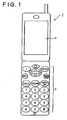
- Fig. 1 is a view showing the basic configuration of a mobile terminal device.
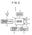
- Fig. 2 is a block diagram showing the functions of this mobile terminal device.
- Fig. 3 is a schematic view showing a sectional structure of the key operation section thereof, and
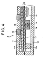
- Fig. 4 is a schematic view showing how heat is transferred.
- Fig. 5 , Fig. 6 , Fig. 8 and Fig. 9 are views showing variations of the sectional structure of the key operation section
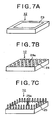
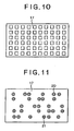
- Figs. 7A, 7B and 7C are schematic perspective views showing the structures of electronic components to be mounted on a circuit board according to this embodiment, and Fig. 10 to Fig.
- Fig. 12 are views showing variations of the shape of a heat conduction layer.
- Fig. 13 is a schematic view showing how heat is transferred in a conventional mobile terminal device.
- a mobile phone is taken as an example of mobile terminal devices and is described below, such mobile terminal devices should only be equipped with at least an operation member and a display means, and the configuration thereof can be applied similarly to any mobile devices, for example, mobile computers such as PDAs, slim digital cameras and mobile game machines.
- a mobile terminal device 1 (mobile phone) generally comprises a display section 3, formed of a liquid crystal display device, an EL light-emitting device or the like, for displaying standby screens, various function setting screens, web screens, etc.; a key operation section 2 having multiple keys, such as numeric keys, direction keys and special function keys; a wireless communications section 8 and an antenna 9 for carrying out telephone communications, E-mail sending/receiving, web screen receiving, etc.; a speaker 4 and a microphone 5 for inputting/outputting sound and for outputting ring tone; an internal storage device 6 for storing various setting values; and a control section 7 for controlling these. Furthermore, various electronic components for realizing various functions of the mobile terminal device 1 are disposed inside the key operation section 2.
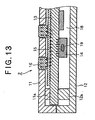
- the sectional structure of the key operation section 2 of the mobile terminal device 1 is as shown in Fig. 3 , for example.
- the key operation section 2 comprises an upper housing 11; a lower housing 12 fitted to the upper housing 11; a circuit board 13 arranged inside the upper housing 11 and the lower housing 12 and held by the protruding portions 11a and 12a of the respective housings; a key sheet 15 provided on a face of the circuit board 13 on the side of the key operation face of the key operation section 2; keys 16, such as numeric keys, direction keys and special function keys, arranged on the key sheet 15; and at least one electronic component 14 arranged on the other face of the circuit board 13 on the opposite side of the key operation face of the key operation section 2.
- Inside the circuit board 13, at least one heat conduction layer 17 having the shape of a layer is provided wherein a member
- a heat conduction member having a heat conductivity at least higher than that of the main constituent material (a material constituting the substrate excluding wiring materials and the like) of the circuit board 13 is arranged in the direction of the face of the circuit board 13.
- this heat conduction member may be formed of a metal material, such as copper or aluminum, or may be formed of a material having high electrical insulation, such as carbon. Furthermore, the heat conduction member may be formed of thin films of these materials, and may also be formed of thin sheets wherein these materials are dispersed in a resin or the like.
- the method for producing the circuit board 13 is not particularly limited, but a method for producing general multi-layer circuit boards may also be used.
- the circuit board 13 can also be produced by using a method wherein two substrates on which wiring patterns are formed beforehand are made, the heat conduction layer 17 is formed on the surface of one of the substrates, and the other substrate is bonded to the heat conduction layer 17 using an adhesive or the like.
- the heat conduction layer 17 is formed at a nearly central position in the thickness direction of the circuit board 13 in the figure, the heat conduction layer 17 should only be formed inside the circuit board 13.
- the heat conduction layer 17 may be formed at a position close to the face on which the electronic components 14 are mounted or may also be formed at a position close to the other face that is close to the key operation face of the key operation section 2.
- the number, size, disposition and the like of the electronic components 14 are not limited.
- the electronic components 14 at least one electronic component 14 generating heat (a heat-generating component whose temperature is raised to a temperature at least higher than the ambient temperature when driven, for example, a power amplifier, a charging IC or the like) should only be included.
- the configuration of each electronic component 14 is not limited.
- the electronic component 14 may be a component for realizing its individual function, such as a transistor or a transformer, or may be an assembly comprising multiple components for realizing their individual functions, such as an amplifier or a voltage converter.
- the electronic components 14 are mounted on only one face of the circuit board 13 in the figure, in the case that there is space on the other face of the circuit board 13 (on the side of the key operation face), the electronic components 14 may also be mounted on the side of key operation face.
- the thickness of the circuit board 13 is sufficiently smaller than the dimensions in the direction of the face, the heat dispersed into the circuit board 13 is promptly transferred to the opposite face of the circuit board 13, and further transferred to the respective keys 16 via the key sheet 15 installed on the opposite face of the circuit board 13. For this reason, only the keys 16 disposed close to the electronic component 14 generating heat and the upper housing 11 in the vicinity thereof tend to be heated to high temperatures.
- the keys 16 are formed separate from the housing (the upper housing 11 in this case) so that they can be pressed.
- the key sheet 15 is disposed separate from the housing so as not to be pressed by anything other than the keys 16.
- the heat generated in the electronic components 14 mounted on one face of the circuit board 13 is similarly transferred to the circuit board 13 since the heat conduction layer 17 being excellent in heat conductivity is arranged in the shape of a layer in the direction of the face of the circuit board 13 inside the circuit board 13, the heat transferred to the circuit board 13 is promptly dispersed in the direction of the face of the circuit board 13 via the heat conduction layer 17. Furthermore, the heat dispersed to the whole of the heat conduction layer 17 is transferred to the whole face on the opposite side of the circuit board 13, and then transferred to all the keys 16 via the key sheet 15.
- the heat is also transferred to the upper housing 11 and the lower housing 12 via the protruding portions 11a and 12a that are used to hold and fix the circuit board 13. For this reason, even if the electronic components 14 generate heat, it is possible to prevent the problem of raising the temperatures of only the keys 16 and the upper housing 11 in the vicinity of the electronic components 14.
- a heat conduction suppressing layer 22 having a given thickness is provided closer to the side of the key operation face than the heat conduction layer 17 inside the circuit board 13, and the heat conducted to the heat conduction layer 17 is radiated to sections other than the key sheet 15 and the keys 16 (for example, the upper housing 11 and the lower housing 12 via the protruding portions 11a and 12a) by the heat conduction suppressing layer 22.
- the temperature rise at the keys 16 can be suppressed.
- the heat conduction suppressing layer 22 may be formed of, for example, a member at least having a heat conductivity smaller than that of the main constituent material of the circuit board 13, or areas having a small heat conductivity may be formed in the circuit board 13 by providing minute pores in the circuit board 13 so as to function as the heat conduction suppressing layer 22.
- connection portion 17a connected to the heat conduction layer 17 is formed at the portion of the circuit board 13 on which the electronic component 14 generating heat is mounted, and the electronic component 14 is mounted so as to make contact with the connection portion 17a (for example, the connection portion 17a is formed so as to protrude from the circuit board 13, and the protruding portion is crushed when the electronic component 14 is mounted).
- connection portion 17a is not particularly limited. However, for example, it may be possible that at least one hole reaching the heat conduction layer 17 from the component mounting face is formed at the portion of the circuit board 13 on which the electronic component 14 is mounted and that a heat conduction member (the member may be the same member as that of the heat conduction layer 17 or may be a member different therefrom) is embedded inside the hole. Furthermore, it may also be possible that at least one through hole passing through the circuit board 13 from the side of the key operation face is formed and that the above-mentioned heat conduction member is embedded inside the through hole.
- connection portion 17a in the case that the connection portion 17a described above is formed, it may also be possible that a member having a high heat conductivity, such as a metal plate 23, is provided beforehand on the component mounting face of the circuit board on which the electronic component 14 is mounted as shown in Fig. 7A and that this metal plate 23 is made so as to contact with the connection portion 17a.
- a member having a high heat conductivity such as a metal plate 23
- BGA All Grid Array
- connection solder ball 24a (the position of the connection solder ball 24a is not limited to that shown in the figure), that a hole reaching the heat conduction layer 17 is formed at the position opposed to the connection solder ball 24a, and that, when the electronic component 14 is mounted, the connection solder ball 24a is melted and embedded inside the hole so as to make contact with the heat conduction layer 17. Furthermore, in the case that the electronic component 14 is connected to the circuit board 13 by pins, it may also be possible that at least one connection pin 25a not contributing to the electrical connections of the electronic component 14 is provided among the pins 25 as shown in Fig.
- connection pin 25a (the position of the connection pin 25a is not limited to that shown in the figure), that a hole reaching the heat conduction layer 17 is formed at the position opposed to the connection pin 25a, and that, when the electronic component 14 is mounted, the connection pin 25a is made so as to contact with the heat conduction layer 17.
- connection solder ball 24a and the connection pin 25a described above may be connected to the housing of the electronic component 14 or a member inside the electronic component 14 (for example, an individual component, an internal circuit board or the like constituting the electronic component 14).
- the generated heat can be transferred promptly to the outside without being stored inside the electronic component 14 by directly thermally contacting the connection solder ball 24a or the connection pin 25a with the heating element inside the electronic component 14. Hence, the temperature rise at the electronic component 14 itself can be suppressed, and the performance of the electronic component 14 can be improved.
- the heat conduction layer 17 should only be formed so that the heat conduction can be facilitated in the direction of the face of the circuit board 13.
- multiple heat conduction layers 17 may also be provided inside the circuit board 13.
- the heat conduction layer 17 may be formed on the whole face of the circuit board 13.
- the heat conduction layer 17 should only be structured so as to expand in the direction of the face of the circuit board 13.
- the heat conduction layer 17 is not necessarily required to be formed on the whole face of the circuit board 13, as long as the heat conduction layer 17 can promptly transfer the heat generated in the electronic components 14 in the direction of the face of the circuit board 13.
- the heat conduction layer 17 may have a grid shape or a slit shape (the grids or slits may have regular shapes or irregular shapes being different in width or pitch).
- the heat conduction layer 17 is formed of a material having high electrical insulation, such as carbon, the heat conduction layer 17 is not short-circuited to the connection wires for connecting the front and back faces of the circuit board 13.
- the heat conduction layer 17 is formed of a metal material, such as copper or aluminum, the heat conduction layer 17 is in danger of being short-circuited to the connection wires.
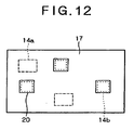
- the heat generated in some of the electronic components 14 is also transferred to the other electronic components 14, thereby raising the temperatures of the other electronic components 14.
- the electronic components 14 are classified into two types: those hardly affected by temperature (heat-resistant components that operate normally or have unvarying characteristics even when the temperature rises) and those easily affected by temperature (non-heat-resistant components that do not operate normally or have characteristics deteriorated when the temperature rises). In the case that these two types of electronic components 14 are mixed together, it is undesirable that the temperatures of the non-heat-resistant components are raised by the heat generated by some of the electronic components 14. To solve this problem, it may be possible that, as shown in Fig.
- the heat conduction layer 17 is formed on the whole face or part of the circuit board 13 excluding the areas on which non-heat-resistant components 14b are mounted, as viewed in the normal direction of the circuit board 13, thereby to prevent the temperatures in the vicinities of the non-heat-resistant components 14b from rising.
- the heat generated in the electronic components 14 can thus be transferred promptly in the direction of the face of the circuit board 13 by arranging at least one heat conduction layer 17 having the shape of a layer inside the circuit board 13 as described above.
- the local temperature rise can be suppressed, the degree of freedom in the selection of the electronic components 14 increases, and it is possible to use electronic components 14 having high performance.
- the rigidity of the circuit board 13 can be raised by forming the circuit board 13 to have a multi-layer structure, whereby the reliability of the mobile terminal device 1 can be enhanced.
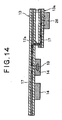
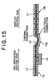
- Fig. 14 and Fig. 15 are sectional views schematically showing the structures of circuit boards inside the mobile terminal device according to the second embodiment.
- a mobile phone is also taken as an example of mobile terminal devices and described below, such mobile terminal devices should only be equipped with at least an operation member and a display means.
- the first embodiment described above is configured so that the heat generated in the electronic components 14 is transferred to the whole of the housing (the upper housing 11 and the lower housing 12) for holding the circuit board 13 on which the electronic components 14 are mounted, the key sheet 15 and the keys 16, whereby the heat is radiated.
- the heat generated in the electronic components 14 is transferred to the other components constituting the mobile terminal device 1.
- the mobile terminal devices 1 of recent years are equipped with a slot for accommodating a recording medium, such as a memory card. Even if the temperature of this slot rises to some extent, no problem occurs in operation.
- a second circuit board 13a equipped with a slot 26 or the like is fixed to the circuit board 13 according to the first embodiment, at least one heat conduction layer 17 (the layer may be the same as or different from the heat conduction layer 17 of the circuit board 13) is also provided inside or on the surface of the second circuit board 13a, and the heat conduction layer 17 of the circuit board 13 is thermally connected to the heat conduction layer 17 of the second circuit board 13a by a thermal connection member (a connection portion 17a also serving as a support rod for fixing the second circuit board 13a, a metal wire or the like).
- a thermal connection member a connection portion 17a also serving as a support rod for fixing the second circuit board 13a, a metal wire or the like.
- the heat generated in the electronic components 14 is transferred from the heat conduction layer 17 inside the circuit board 13 to the heat conduction layer 17 of the second circuit board 13a via the connection portion 17a, the temperature of the slot 26 is raised, and the heat thus is radiated, whereby heat-radiating paths can be increased.
- the mobile terminal devices 1 of recent years mostly have a foldable structure to realize downsizing.
- a mobile phone as shown in Fig. 1 , it is composed of two sections: a section wherein the key operation section 2 is disposed, and a section wherein the display section 3 is disposed.
- the temperature rise at the components that the user touches directly, such as the keys 16, cause problems.
- the sections that the user does not touch directly, such as the display section 3 and the housing for holding the display section 3 do not cause problems even if temperature rises to some extent.
- Fig. 1 the sections that the user does not touch directly, such as the display section 3 and the housing for holding the display section 3
- At least one heat conduction layer 17 (the layer may be the same as or different from the heat conduction layer 17 of the circuit board 13) is also provided inside the circuit board 13b on the display section side, and the circuit board 13 is thermally connected to the circuit board 13b on the display section side by a thermal connection member (the heat conduction layer 17, a metal wire or the like provided inside or on the surface of the flexible circuit board 13c).
- the heat generated in the electronic components 14 mounted on the circuit board 13 is transferred from the heat conduction layer 17 inside the circuit board 13 to the heat conduction layer 17 of the circuit board 13b on the display section side via the flexible circuit board 13c.
- the temperatures of the housing for fixing the circuit board 13b on the display section side and other sections are raised, and the heat is radiated, whereby heat-radiating paths can be increased.
- the circuit board 13 itself may be formed of a material having an excellent heat conductivity in which a heat conduction material is dispersed.
- the mobile terminal device according to each of the embodiments described above is configured so that the keys 16 are disposed on one face of the circuit board 13 via the key sheet 15 and that the electronic components 14 are mounted on the other face, the device may also be configured so that these are disposed on the same face of the circuit board 13.
Landscapes
- Engineering & Computer Science (AREA)
- Theoretical Computer Science (AREA)
- Computer Hardware Design (AREA)
- Human Computer Interaction (AREA)
- Physics & Mathematics (AREA)
- General Engineering & Computer Science (AREA)
- General Physics & Mathematics (AREA)
- Microelectronics & Electronic Packaging (AREA)
- Cooling Or The Like Of Electrical Apparatus (AREA)
- Telephone Set Structure (AREA)
- Structure Of Printed Boards (AREA)
Claims (18)
- Mobiles Endgerät, umfassend:eine Leiterplatte (13), undHitze erzeugende Komponenten (14), die auf der Leiterplatte angebracht sind,des Weiteren umfassendwenigstens eine erste Hitzeleitungsschicht (17), die in der Leiterplatte vorgesehen ist, in der ein Element, das eine Hitzeleitfähigkeit aufweist, die höher ist als die des Materials, das hauptsächlich die Leiterplatte bildet, in der Richtung der Seitenfläche der Leiterplatte angeordnet ist, wobeidie Hitze, die in den Hitze erzeugenden Komponenten erzeugt wird, durch die Hitzeleitungsschicht zu der ganzen Seitenfläche der Leiterplatte verteilt wird,gekennzeichnet durchdes Weiteren eine andere Leiterplatte umfassend,wobei wenigstens eine zweite Hitzeleitungsschicht (17), in der ein Element, das eine Hitzeleitfähigkeit aufweist, die höher ist als die des Materials, das hauptsächlich die andere Leiterplatte bildet, in der Richtung der Seitenfläche der anderen Leiterplatte angeordnet ist, innerhalb oder auf der Oberfläche der anderen Leiterplatte vorgesehen ist, unddie erste Hitzeleitungsschicht der Leiterplatte thermisch mit der zweiten Hitzeleitungsschicht der anderen Leiterplatte durch ein Verbindungselement verbunden ist.
- Mobiles Endgerät nach Anspruch 1, des Weiteren umfassend:ein erstes Gehäuse, in dem die Leiterplatte (13) gehalten wird, ein zweites Gehäuse, wobei die andere Leiterplatte in dem zweiten Gehäuse gehalten wird, und eine Verbindungsleiterplatte zum Verbinden der Leiterplatte (13) mit der anderen Leiterplatte,wenigstens eine dritte Hitzeleitungsschicht, in der ein Element, das eine Hitzeleitfähigkeit aufweist, die höher ist als die des Materials, das hauptsächlich die Verbindungsleiterplatte bildet, in der Richtung der Seitenfläche der Verbindungsleiterplatte angeordnet ist, wobei die dritte Hitzeleitungsschicht innerhalb oder auf der Oberfläche der Verbindungsleiterplatte bereitgestellt ist, undein Verbindungselement, das thermisch zwischen der ersten Hitzeleitungsschicht der Leiterplatte und der zweiten Hitzeleitungsschicht der anderen Leiterplatte durch die dritte Hitzeleitungsschicht der Verbindungsleiterplatte verbindet.
- Mobiles Endgerät nach einem der Ansprüche 1 oder 2, dadurch gekennzeichnet, dass die Hitze erzeugenden Komponenten (14) auf einer Seitenfläche der Leiterplatte (13) angeordnet sind.
- Mobiles Endgerät nach Anspruch 3, des Weiteren umfassend ein Betriebselement (15, 16) auf der anderen Seitenfläche als die Seitenfläche der Leiterplatte, auf der die Hitze erzeugenden Komponenten angeordnet sind, und
wenigstens eine Hitzeleitungsunterdrückungsschicht (22), die eine Hitzeleitfähigkeit aufweist, die niedriger ist als die des Materials, das hauptsächlich die Leiterplatte bildet, wobei die Hitzeleitungsunterdrückungsschicht innerhalb der Leiterplatte und zwischen der ersten Hitzeleitungsschicht und dem Betriebselement vorgesehen ist. - Mobiles Endgerät nach einem der vorstehenden Ansprüche, des Weiteren umfassend ein Verbindungselement (17a), das aus einem Hitzeleitungsmaterial gebildet ist, das eine Hitzeleitfähigkeit aufweist, die höher ist als die des Materials, das hauptsächlich die Leiterplatte bildet, und das Kontakt sowohl mit der ersten Hitzeleitungsschicht (17) als auch den Hitze erzeugenden Komponenten (14) herstellt und zwischen der ersten Hitzeleitungsschicht und den Hitze erzeugenden Komponenten vorgesehen ist, dadurch gekennzeichnet, dass die erste Hitzeleitungsschicht thermisch mit den Hitze erzeugenden Komponenten durch das Verbindungselement verbunden ist.
- Mobiles Endgerät nach einem der vorstehenden Ansprüche, dadurch gekennzeichnet, dass die Hitze erzeugende Komponente (14) mit einem Hitze aussendenden Anschluss ausgestattet ist, der Kontakt mit der Hitzeleitungsschicht in einem Zustand herstellt, dass die Hitze erzeugende Komponente angebracht ist, und die Hitzeleitungsschicht thermisch mit der Hitze erzeugenden Komponente durch den Hitze aussendenden Anschluss verbunden ist.
- Mobiles Endgerät nach Anspruch 6, dadurch gekennzeichnet, dass der Hitze aussendende Anschluss ein Anschluss ist, der zu der elektrischen Verbindung der Hitze erzeugenden Komponenten nicht beiträgt und mit dem Gehäuse der Hitze erzeugenden Komponente oder einer Leiterplatte oder einer Komponente innerhalb der Hitze erzeugenden Komponente verbunden ist.
- Mobiles Endgerät nach Anspruch 7, dadurch gekennzeichnet, dass der Hitze aussendende Anschluss eine Lotkugel ist, die einen Teil eines BGA (Ball Grid Array, Kugelnetzmatrix) bildet.
- Mobiles Endgerät nach einem der vorstehenden Ansprüche, dadurch gekennzeichnet, dass die erste Hitzeleitungsschicht (17) auf der ganzen Seitenfläche oder einem Teil der Leiterplatte gebildet ist, wobei die Bereiche, auf denen Verbindungsdrähte zur Verbindung der Vorder- und der Rückseitenfläche der Leiterplatte gebildet sind, wie in der normalen Richtung der Leiterplatte gesehen, ausgeschlossen sind.
- Mobiles Endgerät nach einem der vorstehenden Ansprüche, des Weiteren umfassend nicht hitzebeständige Komponenten (14b), die auf der Leiterplatte angebracht sind,
dadurch gekennzeichnet, dass
die erste Hitzeleitungsschicht auf der ganzen Seitenfläche oder einem Teil der Leiterplatte gebildet ist, wobei die Bereiche, auf denen die nicht hitzeresistenten Komponenten angebracht sind, wie in der normalen Richtung der Leiterplatte gesehen, ausgeschlossen sind. - Mobiles Endgerät nach einem der vorstehenden Ansprüche, dadurch gekennzeichnet, dass
die Leiterplatte durch vorstehende Abschnitte (11a) befestigt ist, die im voraus auf dem Gehäuse (11, 12) des mobilen Endgeräts vorgesehen sind,
Elemente der Leiterplatte zwischen der ersten Hitzeleitungsschicht und den vorstehenden Abschnitten in wenigstens einem Teil der Bereiche entfernt sind, die den vorstehenden Abschnitten entsprechen, und die erste Hitzeleitungsschicht thermisch mit wenigstens einem Teil der vorstehenden Abschnitte verbunden ist. - Mobiles Endgerät nach einem der vorstehenden Ansprüche, dadurch gekennzeichnet, dass das mobile Endgerät ein Mobiltelefon ist.
- Mobiles Endgerät nach einem der vorstehenden Ansprüche, dadurch gekennzeichnet, dass das mobile Endgerät ein mobiler Computer oder eine mobile Spielekonsole ist.
- Hitzeaussendeverfahren für ein mobiles Endgerät, das mit einer Leiterplatte ausgestattet ist, auf der Hitze erzeugende Komponenten angebracht sind,
wobei das Verfahren innerhalb der Leiterplatte wenigstens eine erste Hitzeleitungsschicht (17) bereitstellt, in der ein Element, das eine Hitzeleitfähigkeit aufweist, die größer ist als die des Materials, das hauptsächlich die Leiterplatte (13) bildet, in der Richtung der Seitenfläche der Leiterplatte angeordnet ist, wodurch die Hitze, die in den Hitze erzeugenden Komponenten (14) erzeugt wird, in der Richtung der Seitenfläche der Leiterplatte durch die erste Hitzeleitungsschicht verteilt wird,
dadurch gekennzeichnet, dass
wenigstens eine zweite Hitzeleitungsschicht (17), in der ein Element, das eine Hitzeleitfähigkeit aufweist, die höher ist als die des Materials, das hauptsächlich die andere Leiterplatte bildet, in der Richtung der Seitenfläche der anderen Leiterplatte bereitgestellt ist, innerhalb oder auf der Oberfläche der anderen Leiterplatte bereitgestellt ist, und
die erste Hitzeleitungsschicht (17) der Leiterplatte thermisch mit der zweiten Hitzeleitungsschicht der anderen Leiterplatte durch ein Verbindungselement verbunden ist. - Hitzeaussendeverfahren nach Anspruch 14,
in dem mobilen Endgerät des Weiteren umfassend ein erstes Gehäuse, zum Halten der Leiterplatte, ein zweites Gehäuse, wobei die andere Leiterplatte in dem zweiten Gehäuse gehalten wird, und eine Verbindungsleiterplatte zum Verbinden der Leiterplatte mit der anderen Leiterplatte,
wobei
wenigstens eine dritte Hitzeleitungsschicht, in der ein Element, das eine Hitzeleitfähigkeit aufweist, die höher ist als die des Materials, das hauptsächlich die Verbindungsleiterplatte bildet, in der Richtung der Seitenfläche der Verbindungsleiterplatte angeordnet ist, innerhalb oder auf der Oberfläche der Verbindungsleiterplatte bereitgestellt ist, und
die erste Hitzeleitungsschicht der Leiterplatte thermisch mit der zweiten Hitzeleitungsschicht der anderen Leiterplatte durch die dritte Hitzeleitungsschicht der Verbindungsleiterplatte durch das Verbindungselement verbunden ist. - Hitzeaussendeverfahren nach Anspruch 14 oder 15, in dem mobilen Endgerät des Weiteren umfassend das Betriebselement (15, 16) auf der anderen Seitenfläche als die Seitenfläche der Leiterplatte, auf der die Hitze erzeugenden Komponenten angebracht sind, dadurch gekennzeichnet, dass
wenigstens eine Hitzeleitungsunterdrückungsschicht, die eine Hitzeleitfähigkeit aufweist, die geringer ist als die des Materials, das hauptsächlich die Leiterplatte bildet, in der Leiterplatte und zwischen der Hitzeleitungsschicht und dem Betriebselement bereitgestellt ist, und die Übertragung der Hitze, die in den Hitze erzeugenden Komponenten erzeugt wird, zu dem Betriebselement durch die Hitzeleitungsunterdrückungsschicht unterdrückt wird. - Hitzeaussendeverfahren nach einem der Ansprüche 14 bis 16, dadurch gekennzeichnet, dass die Hitzeleitungsschicht thermisch mit den Hitze erzeugenden Komponenten durch ein weiteres Verbindungselement verbunden ist, das aus einem Element gebildet ist, das eine Hitzeleitfähigkeit aufweist, die höher ist als die des Materials, das hauptsächlich die Leiterplatte bildet, und die Hitze, die in den Hitze erzeugenden Komponenten erzeugt wird, zu der Hitzeleitungsschicht durch das weitere Verbindungselement übertragen wird.
- Hitzeaussendeverfahren nach einem der Ansprüche 14 bis 17, dadurch gekennzeichnet, dass vorstehende Abschnitte (11a, 12a) zum Befestigen der Leiterplatte auf dem Gehäuse des mobilen Endgeräts bereitgestellt sind, die Elemente der Leiterplatte zwischen der ersten Hitzeleitungsschicht und den vorstehenden Abschnitten in wenigstens einem Teil der Bereiche entfernt sind, die den vorstehenden Abschnitten entsprechen, so dass die erste Hitzeleitungsschicht thermisch mit den vorstehenden Abschnitten verbunden ist, und die Hitze, die in den Hitze erzeugenden Komponenten erzeugt wird, zu dem Gehäuse durch die erste Hitzeleitungsschicht und die vorstehenden Abschnitte übertragen wird.
Applications Claiming Priority (2)
| Application Number | Priority Date | Filing Date | Title |
|---|---|---|---|
| JP2004362272A JP4556174B2 (ja) | 2004-12-15 | 2004-12-15 | 携帯端末機器及び放熱方法 |
| EP05027375A EP1672464B1 (de) | 2004-12-15 | 2005-12-14 | Mobiles Endgerät und Verfahren zur Abstrahlung dessen Wärme |
Related Parent Applications (1)
| Application Number | Title | Priority Date | Filing Date |
|---|---|---|---|
| EP05027375.4 Division | 2005-12-14 |
Publications (2)
| Publication Number | Publication Date |
|---|---|
| EP2365415A1 EP2365415A1 (de) | 2011-09-14 |
| EP2365415B1 true EP2365415B1 (de) | 2013-02-20 |
Family
ID=35677306
Family Applications (3)
| Application Number | Title | Priority Date | Filing Date |
|---|---|---|---|
| EP11004734A Expired - Lifetime EP2365414B1 (de) | 2004-12-15 | 2005-12-14 | Mobiles Endgerät und Verfahren zur Abstrahlung dessen Wärme |
| EP11004735A Expired - Lifetime EP2365415B1 (de) | 2004-12-15 | 2005-12-14 | Mobiles Endgerät und Verfahren zur Abstrahlung dessen Wärme |
| EP05027375A Expired - Lifetime EP1672464B1 (de) | 2004-12-15 | 2005-12-14 | Mobiles Endgerät und Verfahren zur Abstrahlung dessen Wärme |
Family Applications Before (1)
| Application Number | Title | Priority Date | Filing Date |
|---|---|---|---|
| EP11004734A Expired - Lifetime EP2365414B1 (de) | 2004-12-15 | 2005-12-14 | Mobiles Endgerät und Verfahren zur Abstrahlung dessen Wärme |
Family Applications After (1)
| Application Number | Title | Priority Date | Filing Date |
|---|---|---|---|
| EP05027375A Expired - Lifetime EP1672464B1 (de) | 2004-12-15 | 2005-12-14 | Mobiles Endgerät und Verfahren zur Abstrahlung dessen Wärme |
Country Status (4)
| Country | Link |
|---|---|
| US (3) | US7330354B2 (de) |
| EP (3) | EP2365414B1 (de) |
| JP (1) | JP4556174B2 (de) |
| CN (1) | CN100505781C (de) |
Families Citing this family (96)
| Publication number | Priority date | Publication date | Assignee | Title |
|---|---|---|---|---|
| US20060191894A1 (en) * | 2005-02-28 | 2006-08-31 | Sanyo Electric Co., Ltd. | Electronic appliance using heat radiation plate |
| TWI318338B (en) * | 2005-05-19 | 2009-12-11 | Htc Corp | Portable electronic device |
| TWI283806B (en) * | 2005-06-07 | 2007-07-11 | Htc Corp | Portable electronic device |
| JP2007156709A (ja) * | 2005-12-02 | 2007-06-21 | Oki Electric Ind Co Ltd | キーボード装置 |
| JP2007325344A (ja) * | 2006-05-30 | 2007-12-13 | Yazaki Corp | 電気接続箱 |
| CN101502193B (zh) * | 2006-07-25 | 2011-09-21 | 松下电器产业株式会社 | 电路板和移动电子设备 |
| US7978467B2 (en) * | 2007-02-05 | 2011-07-12 | Panasonic Corporation | Key sheet, press switch and electronic device provided with the press switch |
| KR101390082B1 (ko) | 2007-08-01 | 2014-05-28 | 삼성전자주식회사 | 프로젝터를 구비하는 이동통신 단말기 |
| US7764493B2 (en) * | 2008-01-04 | 2010-07-27 | Apple Inc. | Systems and methods for cooling electronic devices using airflow dividers |
| JP4466744B2 (ja) * | 2008-02-06 | 2010-05-26 | 株式会社デンソー | 電子装置の放熱構造 |
| JP4888413B2 (ja) * | 2008-02-14 | 2012-02-29 | 富士通株式会社 | 携帯型電子装置 |
| US8773864B2 (en) * | 2008-06-18 | 2014-07-08 | Lockheed Martin Corporation | Enclosure assembly housing at least one electronic board assembly and systems using same |
| US8189345B2 (en) * | 2008-06-18 | 2012-05-29 | Lockheed Martin Corporation | Electronics module, enclosure assembly housing same, and related systems and methods |
| US9426930B2 (en) * | 2010-12-07 | 2016-08-23 | Hewlett-Packard Development Company, L.P. | Dissipating heat within housings for electrical components |
| US8133621B2 (en) | 2009-02-27 | 2012-03-13 | Research In Motion Limited | Location of a fuel cell on a mobile device |
| EP2224525B1 (de) | 2009-02-27 | 2015-01-14 | BlackBerry Limited | Standorterkennung einer Kraftstoffzelle in einer mobilen Vorrichtung |
| JP5218657B2 (ja) * | 2009-06-15 | 2013-06-26 | 富士通オプティカルコンポーネンツ株式会社 | 光モジュール |
| KR101580126B1 (ko) * | 2009-07-21 | 2015-12-28 | 엘지전자 주식회사 | 이동 단말기 |
| US8787022B2 (en) * | 2009-07-24 | 2014-07-22 | Kabushiki Kaisha Toshiba | Semiconductor storage device and method of manufacturing the same |
| KR101084230B1 (ko) * | 2009-11-16 | 2011-11-16 | 삼성모바일디스플레이주식회사 | 유기 발광 표시 장치 및 유기 발광 표시 장치의 제조 방법 |
| TWI377465B (en) * | 2010-03-11 | 2012-11-21 | Delta Electronics Inc | Heat dissipating module and electronic device using such heat dissipating module |
| KR101803871B1 (ko) * | 2010-11-16 | 2017-12-04 | 엘지전자 주식회사 | 이동 단말기 및 그 제조방법 |
| US8675363B2 (en) * | 2011-07-26 | 2014-03-18 | Hewlett-Packard Development Company, L.P. | Thermal conductors in electronic devices |
| CN102427159A (zh) * | 2011-08-12 | 2012-04-25 | 华为终端有限公司 | 无线终端及其天线架 |
| KR101450950B1 (ko) * | 2011-10-04 | 2014-10-16 | 엘지디스플레이 주식회사 | 드라이버 패키지 |
| KR101861278B1 (ko) * | 2012-03-22 | 2018-05-25 | 엘지전자 주식회사 | 이동 단말기 |
| JP6070977B2 (ja) * | 2012-05-21 | 2017-02-01 | 日本精機株式会社 | 電子回路装置 |
| KR101994931B1 (ko) * | 2012-07-19 | 2019-07-01 | 삼성전자주식회사 | 기억 장치 |
| JP5939102B2 (ja) * | 2012-09-18 | 2016-06-22 | 富士通株式会社 | 電子機器 |
| KR101367067B1 (ko) * | 2012-10-29 | 2014-02-24 | 삼성전기주식회사 | 전력 모듈 패키지 |
| US9342119B1 (en) * | 2013-02-25 | 2016-05-17 | Marvell International Ltd. | Method and apparatus for dissipating heat in a mobile device |
| US10303227B2 (en) | 2013-02-27 | 2019-05-28 | Dell Products L.P. | Information handling system housing heat spreader |
| USD758372S1 (en) * | 2013-03-13 | 2016-06-07 | Nagrastar Llc | Smart card interface |
| USD759022S1 (en) * | 2013-03-13 | 2016-06-14 | Nagrastar Llc | Smart card interface |
| USD729808S1 (en) * | 2013-03-13 | 2015-05-19 | Nagrastar Llc | Smart card interface |
| TWM467917U (zh) * | 2013-06-17 | 2013-12-11 | Giant Technology Co Ltd | 運用於電子罩蓋之多重散熱組件結構 |
| JP2015012161A (ja) * | 2013-06-28 | 2015-01-19 | 株式会社デンソー | 電子装置 |
| CN104640414A (zh) * | 2013-11-11 | 2015-05-20 | 富泰华精密电子(郑州)有限公司 | 移动终端 |
| US9282681B2 (en) | 2014-01-21 | 2016-03-08 | Seagate Technology Llc | Dissipating heat during device operation |
| EP2914071A1 (de) * | 2014-02-28 | 2015-09-02 | AT & S Austria Technologie & Systemtechnik Aktiengesellschaft | Wärmeverteiler in mehrschichtigen Wärmeaufbauten |
| US9930785B2 (en) * | 2014-10-15 | 2018-03-27 | AzTrong Inc. | Configurable heat conducting path for portable electronic device |
| US20160135282A1 (en) * | 2014-11-07 | 2016-05-12 | Kabushiki Kaisha Toshiba | Electronic apparatus |
| CN105704978A (zh) * | 2014-11-26 | 2016-06-22 | 英业达科技有限公司 | 电子装置 |
| JP6330690B2 (ja) * | 2015-02-19 | 2018-05-30 | 株式会社オートネットワーク技術研究所 | 基板ユニット |
| JP2016157715A (ja) * | 2015-02-23 | 2016-09-01 | 日本精工株式会社 | 放熱基板及びこれを収納する放熱ケース。 |
| US9560737B2 (en) | 2015-03-04 | 2017-01-31 | International Business Machines Corporation | Electronic package with heat transfer element(s) |
| USD780763S1 (en) * | 2015-03-20 | 2017-03-07 | Nagrastar Llc | Smart card interface |
| USD864968S1 (en) | 2015-04-30 | 2019-10-29 | Echostar Technologies L.L.C. | Smart card interface |
| JP2016213375A (ja) * | 2015-05-12 | 2016-12-15 | 日本精工株式会社 | 放熱基板及びこれを収納する放熱ケース。 |
| US10426037B2 (en) | 2015-07-15 | 2019-09-24 | International Business Machines Corporation | Circuitized structure with 3-dimensional configuration |
| CN105100315A (zh) * | 2015-08-12 | 2015-11-25 | 小米科技有限责任公司 | 一种移动终端外壳 |
| US20170075397A1 (en) * | 2015-09-14 | 2017-03-16 | Qualcomm Incorporated | Circuits and methods providing temperature mitigation for computing devices |
| US9578764B1 (en) | 2015-09-25 | 2017-02-21 | International Business Machines Corporation | Enclosure with inner tamper-respondent sensor(s) and physical security element(s) |
| US9911012B2 (en) | 2015-09-25 | 2018-03-06 | International Business Machines Corporation | Overlapping, discrete tamper-respondent sensors |
| US9924591B2 (en) | 2015-09-25 | 2018-03-20 | International Business Machines Corporation | Tamper-respondent assemblies |
| US9894749B2 (en) | 2015-09-25 | 2018-02-13 | International Business Machines Corporation | Tamper-respondent assemblies with bond protection |
| US10098235B2 (en) | 2015-09-25 | 2018-10-09 | International Business Machines Corporation | Tamper-respondent assemblies with region(s) of increased susceptibility to damage |
| US10175064B2 (en) | 2015-09-25 | 2019-01-08 | International Business Machines Corporation | Circuit boards and electronic packages with embedded tamper-respondent sensor |
| US10172239B2 (en) | 2015-09-25 | 2019-01-01 | International Business Machines Corporation | Tamper-respondent sensors with formed flexible layer(s) |
| US9591776B1 (en) | 2015-09-25 | 2017-03-07 | International Business Machines Corporation | Enclosure with inner tamper-respondent sensor(s) |
| US10143090B2 (en) | 2015-10-19 | 2018-11-27 | International Business Machines Corporation | Circuit layouts of tamper-respondent sensors |
| US9978231B2 (en) | 2015-10-21 | 2018-05-22 | International Business Machines Corporation | Tamper-respondent assembly with protective wrap(s) over tamper-respondent sensor(s) |
| CN105283040B (zh) * | 2015-10-23 | 2019-04-26 | 联想(北京)有限公司 | 一种散热单元和电子设备 |
| CN205378459U (zh) * | 2015-11-11 | 2016-07-06 | 海能达通信股份有限公司 | 发热器件散热装置、移动终端及功放散热组件 |
| US9913389B2 (en) | 2015-12-01 | 2018-03-06 | International Business Corporation Corporation | Tamper-respondent assembly with vent structure |
| US10327343B2 (en) | 2015-12-09 | 2019-06-18 | International Business Machines Corporation | Applying pressure to adhesive using CTE mismatch between components |
| US9555606B1 (en) | 2015-12-09 | 2017-01-31 | International Business Machines Corporation | Applying pressure to adhesive using CTE mismatch between components |
| US9554477B1 (en) | 2015-12-18 | 2017-01-24 | International Business Machines Corporation | Tamper-respondent assemblies with enclosure-to-board protection |
| US9916744B2 (en) | 2016-02-25 | 2018-03-13 | International Business Machines Corporation | Multi-layer stack with embedded tamper-detect protection |
| US9904811B2 (en) | 2016-04-27 | 2018-02-27 | International Business Machines Corporation | Tamper-proof electronic packages with two-phase dielectric fluid |
| US9881880B2 (en) | 2016-05-13 | 2018-01-30 | International Business Machines Corporation | Tamper-proof electronic packages with stressed glass component substrate(s) |
| US9913370B2 (en) | 2016-05-13 | 2018-03-06 | International Business Machines Corporation | Tamper-proof electronic packages formed with stressed glass |
| US9858776B1 (en) | 2016-06-28 | 2018-01-02 | International Business Machines Corporation | Tamper-respondent assembly with nonlinearity monitoring |
| KR101841836B1 (ko) * | 2016-07-05 | 2018-03-26 | 김구용 | 다면 방열구조를 갖는 pcb 모듈, 및 이 모듈에 사용되는 방열 플레이트, 다층 pcb 어셈블리, 및 모듈 케이스 |
| US10321589B2 (en) | 2016-09-19 | 2019-06-11 | International Business Machines Corporation | Tamper-respondent assembly with sensor connection adapter |
| US10271424B2 (en) | 2016-09-26 | 2019-04-23 | International Business Machines Corporation | Tamper-respondent assemblies with in situ vent structure(s) |
| US10299372B2 (en) | 2016-09-26 | 2019-05-21 | International Business Machines Corporation | Vented tamper-respondent assemblies |
| US9999124B2 (en) | 2016-11-02 | 2018-06-12 | International Business Machines Corporation | Tamper-respondent assemblies with trace regions of increased susceptibility to breaking |
| US10327329B2 (en) | 2017-02-13 | 2019-06-18 | International Business Machines Corporation | Tamper-respondent assembly with flexible tamper-detect sensor(s) overlying in-situ-formed tamper-detect sensor |
| DE102017202329A1 (de) * | 2017-02-14 | 2018-08-16 | Zf Friedrichshafen Ag | Multilayer-Leiterplatte sowie elektronische Anordnung mit einer solchen |
| CN107949240A (zh) * | 2017-11-13 | 2018-04-20 | 广东美晨通讯有限公司 | 终端支架以及终端 |
| JP2019102485A (ja) * | 2017-11-28 | 2019-06-24 | 株式会社村田製作所 | 電子装置 |
| US10306753B1 (en) | 2018-02-22 | 2019-05-28 | International Business Machines Corporation | Enclosure-to-board interface with tamper-detect circuit(s) |
| US11122682B2 (en) | 2018-04-04 | 2021-09-14 | International Business Machines Corporation | Tamper-respondent sensors with liquid crystal polymer layers |
| WO2019198860A1 (ko) * | 2018-04-09 | 2019-10-17 | 엘지전자 주식회사 | 이동 단말기 |
| CN108632412B (zh) * | 2018-05-15 | 2020-01-21 | 维沃移动通信有限公司 | 一种摄像装置及移动终端 |
| JP2022506066A (ja) | 2018-11-05 | 2022-01-17 | ザ ユニバーシティ オブ ノース カロライナ アット チャペル ヒル | 最適化されたfig4遺伝子および発現カセットならびにそれらの使用 |
| WO2020148800A1 (ja) * | 2019-01-15 | 2020-07-23 | 三菱電機株式会社 | 制御装置 |
| KR20210142456A (ko) | 2020-05-18 | 2021-11-25 | 삼성전자주식회사 | 방열 구조체를 포함하는 폴더블 전자 장치 |
| EP3934395A1 (de) * | 2020-07-03 | 2022-01-05 | Eltek AS | Elektrisches schaltungssystem mit einem kühlsystem zum kühlen eines auf eine leiterplatte gelöteten elektrischen bauteils |
| CN118450670A (zh) * | 2020-11-30 | 2024-08-06 | 华为技术有限公司 | 散热装置和电子设备 |
| WO2022217055A1 (en) * | 2021-04-09 | 2022-10-13 | Murata Manufacturing Co., Ltd. | Circuit assembly including gallium nitride devices |
| CN114501202A (zh) * | 2022-02-16 | 2022-05-13 | 展讯通信(上海)有限公司 | 一种扬声器模组及智能终端设备 |
| JP7793132B2 (ja) * | 2022-06-29 | 2026-01-05 | 株式会社オートネットワーク技術研究所 | コネクタ装置 |
| CN117881077B (zh) * | 2024-03-12 | 2024-05-28 | 北京钧天航宇技术有限公司 | 一种一体化热控结构及有源设备 |
| TWI896338B (zh) * | 2024-09-13 | 2025-09-01 | 大陸商慶鼎精密電子(淮安)有限公司 | 具有定向導熱功能的電路板元件及其製作方法 |
Family Cites Families (77)
| Publication number | Priority date | Publication date | Assignee | Title |
|---|---|---|---|---|
| US3760091A (en) * | 1971-11-16 | 1973-09-18 | Ibm | Multilayer circuit board |
| US4388136A (en) * | 1980-09-26 | 1983-06-14 | Sperry Corporation | Method of making a polyimide/glass hybrid printed circuit board |
| US4464704A (en) * | 1980-09-26 | 1984-08-07 | Sperry Corporation | Polyimide/glass-epoxy/glass hybrid printed circuit board |
| US4812792A (en) * | 1983-12-22 | 1989-03-14 | Trw Inc. | High-frequency multilayer printed circuit board |
| US4591659A (en) * | 1983-12-22 | 1986-05-27 | Trw Inc. | Multilayer printed circuit board structure |
| JPS6255606A (ja) | 1985-09-04 | 1987-03-11 | Tohoku Metal Ind Ltd | 偏光子 |
| DE3606591A1 (de) * | 1986-02-28 | 1987-09-10 | Bayerische Motoren Werke Ag | Heiz- und kuehlvorrichtung fuer kraftfahrzeuge |
| US4810563A (en) * | 1986-03-14 | 1989-03-07 | The Bergquist Company | Thermally conductive, electrically insulative laminate |
| JPH0627995Y2 (ja) * | 1986-03-20 | 1994-07-27 | 株式会社東芝 | シ−ルド構造 |
| JPS63120760A (ja) | 1986-11-11 | 1988-05-25 | Nippon Kayaku Co Ltd | フルオレン化合物及びそれを用いた記録材料 |
| US4775596A (en) * | 1987-02-18 | 1988-10-04 | Corning Glass Works | Composite substrate for integrated circuits |
| JPS63162563U (de) * | 1987-04-13 | 1988-10-24 | ||
| SU1638817A1 (ru) * | 1987-11-23 | 1991-03-30 | Харьковский политехнический институт им.В.И.Ленина | Радиоэлектронный блок |
| JPH01195871A (ja) | 1988-01-29 | 1989-08-07 | Toshihiko Yayama | 健康促進器 |
| US4963697A (en) * | 1988-02-12 | 1990-10-16 | Texas Instruments Incorporated | Advanced polymers on metal printed wiring board |
| US4882454A (en) * | 1988-02-12 | 1989-11-21 | Texas Instruments Incorporated | Thermal interface for a printed wiring board |
| JPH0215700A (ja) * | 1988-07-04 | 1990-01-19 | Mitsubishi Electric Corp | 印刷配線板 |
| JPH0241491U (de) * | 1988-09-14 | 1990-03-22 | ||
| JPH02262724A (ja) | 1989-04-03 | 1990-10-25 | Mitsubishi Electric Corp | 携帯無線装置の筐体 |
| US5258887A (en) * | 1992-06-15 | 1993-11-02 | Eaton Corporation | Electrical device cooling system using a heat sink attached to a circuit board containing heat conductive layers and channels |
| US5285352A (en) * | 1992-07-15 | 1994-02-08 | Motorola, Inc. | Pad array semiconductor device with thermal conductor and process for making the same |
| DE9300865U1 (de) * | 1993-01-22 | 1994-05-26 | Siemens AG, 80333 München | Einstückiges Kunststoffteil, insbesondere Spritzgießteil |
| JPH0774439A (ja) * | 1993-09-01 | 1995-03-17 | Nippon Telegr & Teleph Corp <Ntt> | 熱誘導パス付き回路基板 |
| JPH07162181A (ja) * | 1993-12-02 | 1995-06-23 | Fujitsu Ltd | 電子モジュールの電磁波漏洩防止方法 |
| KR0126781Y1 (ko) * | 1994-08-23 | 1999-05-01 | 이형도 | 반도체소자 방열장치 |
| DE69508911T2 (de) * | 1994-11-28 | 1999-10-07 | Kabushiki Kaisha Toshiba, Kawasaki | Gehäuse mit elektromagnetischer Abschirmung |
| DE4446594A1 (de) * | 1994-12-24 | 1996-06-27 | Bosch Gmbh Robert | Elektrisches Gerät |
| JP3004578B2 (ja) * | 1995-05-12 | 2000-01-31 | 財団法人工業技術研究院 | 熱放散増強のための多熱導伝路とパッケージ統合性及び信頼性向上のための縁の周りを囲むキャップからなる集積回路パッケージ |
| JPH10150283A (ja) * | 1996-11-19 | 1998-06-02 | Nec Eng Ltd | 印刷配線基板の放熱構造 |
| JP3106120B2 (ja) * | 1997-05-16 | 2000-11-06 | 三菱電機株式会社 | 携帯型電子機器 |
| US6008536A (en) * | 1997-06-23 | 1999-12-28 | Lsi Logic Corporation | Grid array device package including advanced heat transfer mechanisms |
| JPH1140901A (ja) * | 1997-07-23 | 1999-02-12 | Sharp Corp | 回路基板 |
| JPH1195871A (ja) | 1997-09-17 | 1999-04-09 | Matsushita Electric Ind Co Ltd | 電子機器の放熱構造 |
| JPH1197870A (ja) * | 1997-09-19 | 1999-04-09 | Mitsubishi Heavy Ind Ltd | 電子装置 |
| US6011691A (en) * | 1998-04-23 | 2000-01-04 | Lockheed Martin Corporation | Electronic component assembly and method for low cost EMI and capacitive coupling elimination |
| JP3438582B2 (ja) * | 1998-04-28 | 2003-08-18 | 株式会社日立製作所 | 携帯型パーソナルコンピュータ |
| JP4030651B2 (ja) * | 1998-05-12 | 2008-01-09 | 三菱電機株式会社 | 携帯型電話機 |
| US6257329B1 (en) * | 1998-08-17 | 2001-07-10 | Alfiero Balzano | Thermal management system |
| JP3602968B2 (ja) * | 1998-08-18 | 2004-12-15 | 沖電気工業株式会社 | 半導体装置およびその基板接続構造 |
| JP2000148307A (ja) * | 1998-11-10 | 2000-05-26 | Sony Corp | キーボード |
| TW410446B (en) * | 1999-01-21 | 2000-11-01 | Siliconware Precision Industries Co Ltd | BGA semiconductor package |
| JP2000253115A (ja) | 1999-03-01 | 2000-09-14 | Sony Corp | 携帯電子機器 |
| TW413874B (en) * | 1999-04-12 | 2000-12-01 | Siliconware Precision Industries Co Ltd | BGA semiconductor package having exposed heat dissipation layer and its manufacturing method |
| US6340796B1 (en) * | 1999-06-02 | 2002-01-22 | Northrop Grumman Corporation | Printed wiring board structure with integral metal matrix composite core |
| US6207904B1 (en) * | 1999-06-02 | 2001-03-27 | Northrop Grumman Corporation | Printed wiring board structure having continuous graphite fibers |
| CN100393183C (zh) | 1999-06-21 | 2008-06-04 | 三菱电机株式会社 | 电路形成基板制造方法 |
| US6212071B1 (en) * | 1999-08-20 | 2001-04-03 | Lucent Technologies, Inc. | Electrical circuit board heat dissipation system |
| DE19960246A1 (de) * | 1999-12-14 | 2001-07-05 | Infineon Technologies Ag | Gehäuseanordnung eines Halbleiterbausteins |
| JP4142227B2 (ja) * | 2000-01-28 | 2008-09-03 | サンデン株式会社 | 車両用電動圧縮機のモータ駆動用インバータ装置 |
| DE10017925A1 (de) * | 2000-04-11 | 2001-10-25 | Infineon Technologies Ag | Vorrichtung zum Befestigen einer Wärmeverteilungsabdeckung auf einer Leiterplatte |
| JP2001320171A (ja) * | 2000-05-08 | 2001-11-16 | Shinko Electric Ind Co Ltd | 多層配線基板及び半導体装置 |
| US6696643B2 (en) * | 2000-08-01 | 2004-02-24 | Mitsubishi Denki Kabushiki Kaisha | Electronic apparatus |
| TW462121B (en) * | 2000-09-19 | 2001-11-01 | Siliconware Precision Industries Co Ltd | Heat sink type ball grid array package |
| US6605778B2 (en) * | 2000-10-02 | 2003-08-12 | Siemens Aktiengesellschaft | Circuit carrier, in particular printed circuit board |
| TW490820B (en) * | 2000-10-04 | 2002-06-11 | Advanced Semiconductor Eng | Heat dissipation enhanced ball grid array package |
| TW511405B (en) * | 2000-12-27 | 2002-11-21 | Matsushita Electric Industrial Co Ltd | Device built-in module and manufacturing method thereof |
| JP2002323936A (ja) | 2001-04-25 | 2002-11-08 | Casio Comput Co Ltd | 携帯型情報機器のキャリングケース |
| JP2002368440A (ja) | 2001-06-06 | 2002-12-20 | Toshiba Corp | 折り畳み型電子機器とそのフレキシブル基板 |
| US6548190B2 (en) * | 2001-06-15 | 2003-04-15 | General Electric Company | Low thermal conductivity thermal barrier coating system and method therefor |
| JP4601879B2 (ja) * | 2001-09-14 | 2010-12-22 | パナソニック株式会社 | 携帯電子機器及びbgaパッケージ保護装置 |
| JP3937840B2 (ja) * | 2002-01-10 | 2007-06-27 | 株式会社日立製作所 | 高周波モジュール |
| US6657311B1 (en) * | 2002-05-16 | 2003-12-02 | Texas Instruments Incorporated | Heat dissipating flip-chip ball grid array |
| US6809416B1 (en) * | 2002-05-28 | 2004-10-26 | Intersil Corporation | Package for integrated circuit with thermal vias and method thereof |
| US7138711B2 (en) * | 2002-06-17 | 2006-11-21 | Micron Technology, Inc. | Intrinsic thermal enhancement for FBGA package |
| US7023699B2 (en) * | 2002-06-10 | 2006-04-04 | Visteon Global Technologies, Inc. | Liquid cooled metal thermal stack for high-power dies |
| JP3888254B2 (ja) * | 2002-07-29 | 2007-02-28 | 富士電機ホールディングス株式会社 | 多層プリント配線板 |
| EP1394857A3 (de) | 2002-08-28 | 2004-04-07 | Matsushita Electric Industrial Co., Ltd. | Halbleiteranordnung |
| JP2004172459A (ja) * | 2002-11-21 | 2004-06-17 | Advics:Kk | 電子制御装置における電子部品の放熱構造 |
| US7248903B2 (en) * | 2002-12-25 | 2007-07-24 | Kyocera Corporation | Mobile instrument with flexible printed wiring board |
| TW559461U (en) * | 2003-01-20 | 2003-10-21 | Power Mate Technology Corp | Heat conducting structure for circuit board |
| JP4186732B2 (ja) * | 2003-07-24 | 2008-11-26 | 株式会社村田製作所 | 電子機器 |
| US6954360B2 (en) * | 2003-08-22 | 2005-10-11 | Nokia Corporation | Thermally enhanced component substrate: thermal bar |
| KR20050039206A (ko) * | 2003-10-24 | 2005-04-29 | 삼성에스디아이 주식회사 | 플라즈마 디스플레이 장치 |
| US6982874B2 (en) * | 2003-11-25 | 2006-01-03 | Advanced Energy Technology Inc. | Thermal solution for electronic devices |
| US7228894B2 (en) * | 2004-04-30 | 2007-06-12 | Hewlett-Packard Development Company, L.P. | Heat spreader with controlled Z-axis conductivity |
| US20050270746A1 (en) * | 2004-06-04 | 2005-12-08 | Reis Bradley E | Insulating structure having combined insulating and heat spreading capabilities |
| JP4799350B2 (ja) * | 2006-09-29 | 2011-10-26 | 株式会社東芝 | 電子機器 |
-
2004
- 2004-12-15 JP JP2004362272A patent/JP4556174B2/ja not_active Expired - Fee Related
-
2005
- 2005-12-14 EP EP11004734A patent/EP2365414B1/de not_active Expired - Lifetime
- 2005-12-14 EP EP11004735A patent/EP2365415B1/de not_active Expired - Lifetime
- 2005-12-14 EP EP05027375A patent/EP1672464B1/de not_active Expired - Lifetime
- 2005-12-15 US US11/304,179 patent/US7330354B2/en not_active Expired - Fee Related
- 2005-12-15 CN CNB2005101318718A patent/CN100505781C/zh not_active Expired - Fee Related
-
2007
- 2007-11-15 US US11/940,758 patent/US7616446B2/en not_active Expired - Fee Related
-
2009
- 2009-09-25 US US12/567,276 patent/US7903422B2/en not_active Expired - Fee Related
Also Published As
| Publication number | Publication date |
|---|---|
| US20080068810A1 (en) | 2008-03-20 |
| US7330354B2 (en) | 2008-02-12 |
| CN1791133A (zh) | 2006-06-21 |
| EP2365414A1 (de) | 2011-09-14 |
| CN100505781C (zh) | 2009-06-24 |
| EP1672464A2 (de) | 2006-06-21 |
| EP1672464B1 (de) | 2012-04-25 |
| EP2365415A1 (de) | 2011-09-14 |
| US7903422B2 (en) | 2011-03-08 |
| US20060126310A1 (en) | 2006-06-15 |
| JP4556174B2 (ja) | 2010-10-06 |
| JP2006173290A (ja) | 2006-06-29 |
| EP1672464A3 (de) | 2010-12-15 |
| US7616446B2 (en) | 2009-11-10 |
| EP2365414B1 (de) | 2012-12-05 |
| US20100014255A1 (en) | 2010-01-21 |
Similar Documents
| Publication | Publication Date | Title |
|---|---|---|
| EP2365415B1 (de) | Mobiles Endgerät und Verfahren zur Abstrahlung dessen Wärme | |
| JP4498419B2 (ja) | 電子機器 | |
| JP4144983B2 (ja) | 熱拡散プレートを有する薄型電磁妨害シールド | |
| US20080130234A1 (en) | Electronic Apparatus | |
| JP2000269671A (ja) | 電子機器 | |
| JP2008198860A (ja) | 小型携帯端末機器の冷却手段 | |
| CN109219307B (zh) | 散热结构及具有该散热结构的电子装置 | |
| US20040264114A1 (en) | Electronic apparatus including printed wiring board provided with heat generating component | |
| JP4525460B2 (ja) | モバイル機器 | |
| JP2008218618A (ja) | プリント配線板 | |
| EP1732230B1 (de) | Tragbares elektronisches Gerät | |
| JP2010055642A (ja) | 電子機器 | |
| JP2007174526A (ja) | 携帯電子機器の放熱構造 | |
| CN111432615B (zh) | 散热结构和电子设备 | |
| CN113268127A (zh) | 电子设备 | |
| JP2013118296A (ja) | 電子機器 | |
| JPH1098287A (ja) | 回路基板モジュールの冷却装置およびこの冷却装置を有する携帯形電子機器 | |
| JP2007115097A (ja) | 電子機器および基板ユニット | |
| CN223231474U (zh) | 散热件和电子设备 | |
| JP2010287672A (ja) | 携帯電子機器 | |
| US20060191894A1 (en) | Electronic appliance using heat radiation plate | |
| JP2000332169A (ja) | 発熱体の放熱構造及びこれを有する電子機器 | |
| KR20060067240A (ko) | 정전기방전 및 방열수단을 갖춘 키패드를 구비한 이동통신단말기 | |
| JP2002344180A (ja) | 電子機器の放熱構造 | |
| JP2009224720A (ja) | 電子モジュールおよび電子装置 |
Legal Events
| Date | Code | Title | Description |
|---|---|---|---|
| PUAI | Public reference made under article 153(3) epc to a published international application that has entered the european phase |
Free format text: ORIGINAL CODE: 0009012 |
|
| AC | Divisional application: reference to earlier application |
Ref document number: 1672464 Country of ref document: EP Kind code of ref document: P |
|
| AK | Designated contracting states |
Kind code of ref document: A1 Designated state(s): DE FR GB IT |
|
| AX | Request for extension of the european patent |
Extension state: AL BA HR MK YU |
|
| REG | Reference to a national code |
Ref country code: DE Ref legal event code: R079 Ref document number: 602005038260 Country of ref document: DE Free format text: PREVIOUS MAIN CLASS: G06F0001200000 Ipc: H05K0001020000 |
|
| 17P | Request for examination filed |
Effective date: 20120313 |
|
| RIC1 | Information provided on ipc code assigned before grant |
Ipc: H05K 1/02 20060101AFI20120416BHEP |
|
| GRAP | Despatch of communication of intention to grant a patent |
Free format text: ORIGINAL CODE: EPIDOSNIGR1 |
|
| RIN1 | Information on inventor provided before grant (corrected) |
Inventor name: WATANABE, YOUSUKE |
|
| GRAS | Grant fee paid |
Free format text: ORIGINAL CODE: EPIDOSNIGR3 |
|
| GRAP | Despatch of communication of intention to grant a patent |
Free format text: ORIGINAL CODE: EPIDOSNIGR1 |
|
| RBV | Designated contracting states (corrected) |
Designated state(s): DE FR GB |
|
| GRAA | (expected) grant |
Free format text: ORIGINAL CODE: 0009210 |
|
| AC | Divisional application: reference to earlier application |
Ref document number: 1672464 Country of ref document: EP Kind code of ref document: P |
|
| AK | Designated contracting states |
Kind code of ref document: B1 Designated state(s): DE FR GB |
|
| REG | Reference to a national code |
Ref country code: GB Ref legal event code: FG4D |
|
| REG | Reference to a national code |
Ref country code: DE Ref legal event code: R096 Ref document number: 602005038260 Country of ref document: DE Effective date: 20130418 |
|
| PLBE | No opposition filed within time limit |
Free format text: ORIGINAL CODE: 0009261 |
|
| STAA | Information on the status of an ep patent application or granted ep patent |
Free format text: STATUS: NO OPPOSITION FILED WITHIN TIME LIMIT |
|
| 26N | No opposition filed |
Effective date: 20131121 |
|
| REG | Reference to a national code |
Ref country code: DE Ref legal event code: R097 Ref document number: 602005038260 Country of ref document: DE Effective date: 20131121 |
|
| REG | Reference to a national code |
Ref country code: GB Ref legal event code: 732E Free format text: REGISTERED BETWEEN 20141023 AND 20141029 |
|
| REG | Reference to a national code |
Ref country code: FR Ref legal event code: TP Owner name: LENOVO INNOVATIONS LIMITED (HONG KONG), HK Effective date: 20141119 |
|
| PGFP | Annual fee paid to national office [announced via postgrant information from national office to epo] |
Ref country code: FR Payment date: 20141208 Year of fee payment: 10 |
|
| REG | Reference to a national code |
Ref country code: FR Ref legal event code: ST Effective date: 20160831 |
|
| PG25 | Lapsed in a contracting state [announced via postgrant information from national office to epo] |
Ref country code: FR Free format text: LAPSE BECAUSE OF NON-PAYMENT OF DUE FEES Effective date: 20151231 |
|
| PGFP | Annual fee paid to national office [announced via postgrant information from national office to epo] |
Ref country code: DE Payment date: 20161206 Year of fee payment: 12 Ref country code: GB Payment date: 20161214 Year of fee payment: 12 |
|
| REG | Reference to a national code |
Ref country code: DE Ref legal event code: R119 Ref document number: 602005038260 Country of ref document: DE |
|
| GBPC | Gb: european patent ceased through non-payment of renewal fee |
Effective date: 20171214 |
|
| PG25 | Lapsed in a contracting state [announced via postgrant information from national office to epo] |
Ref country code: DE Free format text: LAPSE BECAUSE OF NON-PAYMENT OF DUE FEES Effective date: 20180703 |
|
| PG25 | Lapsed in a contracting state [announced via postgrant information from national office to epo] |
Ref country code: GB Free format text: LAPSE BECAUSE OF NON-PAYMENT OF DUE FEES Effective date: 20171214 |