EP2302452A2 - Fotomaskenrohling und Fotomaske - Google Patents
Fotomaskenrohling und Fotomaske Download PDFInfo
- Publication number
- EP2302452A2 EP2302452A2 EP10196189A EP10196189A EP2302452A2 EP 2302452 A2 EP2302452 A2 EP 2302452A2 EP 10196189 A EP10196189 A EP 10196189A EP 10196189 A EP10196189 A EP 10196189A EP 2302452 A2 EP2302452 A2 EP 2302452A2
- Authority
- EP
- European Patent Office
- Prior art keywords
- film
- light
- transition metal
- shielding film
- photomask blank
- Prior art date
- Legal status (The legal status is an assumption and is not a legal conclusion. Google has not performed a legal analysis and makes no representation as to the accuracy of the status listed.)
- Granted
Links
- 229910052710 silicon Inorganic materials 0.000 claims abstract description 41
- 239000010703 silicon Substances 0.000 claims abstract description 39
- 239000000758 substrate Substances 0.000 claims abstract description 36
- 229910052723 transition metal Inorganic materials 0.000 claims abstract description 36
- 150000003624 transition metals Chemical class 0.000 claims abstract description 36
- 229910052751 metal Inorganic materials 0.000 claims abstract description 12
- 239000002184 metal Substances 0.000 claims abstract description 12
- 230000003667 anti-reflective effect Effects 0.000 claims description 88
- 238000000034 method Methods 0.000 claims description 43
- 238000001312 dry etching Methods 0.000 claims description 37
- XUIMIQQOPSSXEZ-UHFFFAOYSA-N Silicon Chemical compound [Si] XUIMIQQOPSSXEZ-UHFFFAOYSA-N 0.000 claims description 36
- 229910021350 transition metal silicide Inorganic materials 0.000 claims description 35
- 239000011651 chromium Substances 0.000 claims description 28
- 239000010410 layer Substances 0.000 claims description 27
- 230000003287 optical effect Effects 0.000 claims description 25
- 229910052804 chromium Inorganic materials 0.000 claims description 24
- VYZAMTAEIAYCRO-UHFFFAOYSA-N Chromium Chemical compound [Cr] VYZAMTAEIAYCRO-UHFFFAOYSA-N 0.000 claims description 23
- 229910052760 oxygen Inorganic materials 0.000 claims description 19
- IJGRMHOSHXDMSA-UHFFFAOYSA-N Atomic nitrogen Chemical compound N#N IJGRMHOSHXDMSA-UHFFFAOYSA-N 0.000 claims description 18
- QVGXLLKOCUKJST-UHFFFAOYSA-N atomic oxygen Chemical compound [O] QVGXLLKOCUKJST-UHFFFAOYSA-N 0.000 claims description 17
- 239000001301 oxygen Substances 0.000 claims description 17
- ZAMOUSCENKQFHK-UHFFFAOYSA-N Chlorine atom Chemical compound [Cl] ZAMOUSCENKQFHK-UHFFFAOYSA-N 0.000 claims description 13
- 239000000460 chlorine Substances 0.000 claims description 13
- 229910052801 chlorine Inorganic materials 0.000 claims description 13
- 229910052799 carbon Inorganic materials 0.000 claims description 12
- YCKRFDGAMUMZLT-UHFFFAOYSA-N Fluorine atom Chemical compound [F] YCKRFDGAMUMZLT-UHFFFAOYSA-N 0.000 claims description 11
- 239000011737 fluorine Substances 0.000 claims description 11
- 229910052731 fluorine Inorganic materials 0.000 claims description 11
- 229910052750 molybdenum Inorganic materials 0.000 claims description 11
- 229910052757 nitrogen Inorganic materials 0.000 claims description 11
- OKTJSMMVPCPJKN-UHFFFAOYSA-N Carbon Chemical compound [C] OKTJSMMVPCPJKN-UHFFFAOYSA-N 0.000 claims description 10
- ZOKXTWBITQBERF-UHFFFAOYSA-N Molybdenum Chemical compound [Mo] ZOKXTWBITQBERF-UHFFFAOYSA-N 0.000 claims description 10
- 238000004519 manufacturing process Methods 0.000 claims description 10
- 239000011733 molybdenum Substances 0.000 claims description 10
- 229910000423 chromium oxide Inorganic materials 0.000 claims description 8
- -1 chromium oxide nitride Chemical class 0.000 claims description 8
- 229910021344 molybdenum silicide Inorganic materials 0.000 claims description 8
- 150000004767 nitrides Chemical class 0.000 claims description 8
- YXTPWUNVHCYOSP-UHFFFAOYSA-N bis($l^{2}-silanylidene)molybdenum Chemical group [Si]=[Mo]=[Si] YXTPWUNVHCYOSP-UHFFFAOYSA-N 0.000 claims description 5
- PXHVJJICTQNCMI-UHFFFAOYSA-N Nickel Chemical compound [Ni] PXHVJJICTQNCMI-UHFFFAOYSA-N 0.000 claims description 4
- WGLPBDUCMAPZCE-UHFFFAOYSA-N Trioxochromium Chemical compound O=[Cr](=O)=O WGLPBDUCMAPZCE-UHFFFAOYSA-N 0.000 claims description 4
- SJKRCWUQJZIWQB-UHFFFAOYSA-N azane;chromium Chemical compound N.[Cr] SJKRCWUQJZIWQB-UHFFFAOYSA-N 0.000 claims description 4
- 229910052715 tantalum Inorganic materials 0.000 claims description 4
- GUVRBAGPIYLISA-UHFFFAOYSA-N tantalum atom Chemical compound [Ta] GUVRBAGPIYLISA-UHFFFAOYSA-N 0.000 claims description 4
- 239000002356 single layer Substances 0.000 claims description 3
- WFKWXMTUELFFGS-UHFFFAOYSA-N tungsten Chemical compound [W] WFKWXMTUELFFGS-UHFFFAOYSA-N 0.000 claims description 3
- 229910052721 tungsten Inorganic materials 0.000 claims description 3
- 239000010937 tungsten Substances 0.000 claims description 3
- RTAQQCXQSZGOHL-UHFFFAOYSA-N Titanium Chemical compound [Ti] RTAQQCXQSZGOHL-UHFFFAOYSA-N 0.000 claims description 2
- QCWXUUIWCKQGHC-UHFFFAOYSA-N Zirconium Chemical compound [Zr] QCWXUUIWCKQGHC-UHFFFAOYSA-N 0.000 claims description 2
- 229910017052 cobalt Inorganic materials 0.000 claims description 2
- 239000010941 cobalt Substances 0.000 claims description 2
- GUTLYIVDDKVIGB-UHFFFAOYSA-N cobalt atom Chemical compound [Co] GUTLYIVDDKVIGB-UHFFFAOYSA-N 0.000 claims description 2
- 229910052735 hafnium Inorganic materials 0.000 claims description 2
- VBJZVLUMGGDVMO-UHFFFAOYSA-N hafnium atom Chemical compound [Hf] VBJZVLUMGGDVMO-UHFFFAOYSA-N 0.000 claims description 2
- 229910052759 nickel Inorganic materials 0.000 claims description 2
- 229910052758 niobium Inorganic materials 0.000 claims description 2
- 239000010955 niobium Substances 0.000 claims description 2
- GUCVJGMIXFAOAE-UHFFFAOYSA-N niobium atom Chemical compound [Nb] GUCVJGMIXFAOAE-UHFFFAOYSA-N 0.000 claims description 2
- 229910052719 titanium Inorganic materials 0.000 claims description 2
- 239000010936 titanium Substances 0.000 claims description 2
- 229910052720 vanadium Inorganic materials 0.000 claims description 2
- 229910052726 zirconium Inorganic materials 0.000 claims description 2
- LEONUFNNVUYDNQ-UHFFFAOYSA-N vanadium atom Chemical compound [V] LEONUFNNVUYDNQ-UHFFFAOYSA-N 0.000 claims 1
- 239000000463 material Substances 0.000 abstract description 10
- 239000007789 gas Substances 0.000 description 35
- 238000005530 etching Methods 0.000 description 33
- 230000010363 phase shift Effects 0.000 description 30
- 230000008569 process Effects 0.000 description 21
- 238000004544 sputter deposition Methods 0.000 description 21
- 239000000203 mixture Substances 0.000 description 18
- 239000000126 substance Substances 0.000 description 17
- 150000001845 chromium compounds Chemical class 0.000 description 16
- 238000001459 lithography Methods 0.000 description 16
- 230000000052 comparative effect Effects 0.000 description 15
- MHAJPDPJQMAIIY-UHFFFAOYSA-N hydrogen peroxide Substances OO MHAJPDPJQMAIIY-UHFFFAOYSA-N 0.000 description 13
- 238000012545 processing Methods 0.000 description 13
- 238000004140 cleaning Methods 0.000 description 12
- VYPSYNLAJGMNEJ-UHFFFAOYSA-N Silicium dioxide Chemical compound O=[Si]=O VYPSYNLAJGMNEJ-UHFFFAOYSA-N 0.000 description 8
- 230000008859 change Effects 0.000 description 8
- 150000001875 compounds Chemical class 0.000 description 8
- XEMZLVDIUVCKGL-UHFFFAOYSA-N hydrogen peroxide;sulfuric acid Chemical compound OO.OS(O)(=O)=O XEMZLVDIUVCKGL-UHFFFAOYSA-N 0.000 description 7
- QAOWNCQODCNURD-UHFFFAOYSA-N Sulfuric acid Chemical compound OS(O)(=O)=O QAOWNCQODCNURD-UHFFFAOYSA-N 0.000 description 6
- 230000009467 reduction Effects 0.000 description 6
- 229910021332 silicide Inorganic materials 0.000 description 6
- KZBUYRJDOAKODT-UHFFFAOYSA-N Chlorine Chemical compound ClCl KZBUYRJDOAKODT-UHFFFAOYSA-N 0.000 description 5
- SWXQKHHHCFXQJF-UHFFFAOYSA-N azane;hydrogen peroxide Chemical compound [NH4+].[O-]O SWXQKHHHCFXQJF-UHFFFAOYSA-N 0.000 description 5
- 238000000206 photolithography Methods 0.000 description 5
- 239000004065 semiconductor Substances 0.000 description 5
- FVBUAEGBCNSCDD-UHFFFAOYSA-N silicide(4-) Chemical compound [Si-4] FVBUAEGBCNSCDD-UHFFFAOYSA-N 0.000 description 5
- VHUUQVKOLVNVRT-UHFFFAOYSA-N Ammonium hydroxide Chemical compound [NH4+].[OH-] VHUUQVKOLVNVRT-UHFFFAOYSA-N 0.000 description 4
- XKRFYHLGVUSROY-UHFFFAOYSA-N Argon Chemical compound [Ar] XKRFYHLGVUSROY-UHFFFAOYSA-N 0.000 description 4
- QGZKDVFQNNGYKY-UHFFFAOYSA-N ammonia Natural products N QGZKDVFQNNGYKY-UHFFFAOYSA-N 0.000 description 4
- 239000003795 chemical substances by application Substances 0.000 description 4
- 238000002834 transmittance Methods 0.000 description 4
- 229910016006 MoSi Inorganic materials 0.000 description 3
- 125000003118 aryl group Chemical group 0.000 description 3
- 239000011248 coating agent Substances 0.000 description 3
- 238000000576 coating method Methods 0.000 description 3
- 239000013078 crystal Substances 0.000 description 3
- 238000000151 deposition Methods 0.000 description 3
- 230000008021 deposition Effects 0.000 description 3
- 230000000694 effects Effects 0.000 description 3
- 238000007689 inspection Methods 0.000 description 3
- 238000012544 monitoring process Methods 0.000 description 3
- 229920002120 photoresistant polymer Polymers 0.000 description 3
- 239000010453 quartz Substances 0.000 description 3
- 238000005546 reactive sputtering Methods 0.000 description 3
- 238000010561 standard procedure Methods 0.000 description 3
- 238000004381 surface treatment Methods 0.000 description 3
- XLYOFNOQVPJJNP-UHFFFAOYSA-N water Substances O XLYOFNOQVPJJNP-UHFFFAOYSA-N 0.000 description 3
- 229910020968 MoSi2 Inorganic materials 0.000 description 2
- 238000013459 approach Methods 0.000 description 2
- 229910052786 argon Inorganic materials 0.000 description 2
- 230000015572 biosynthetic process Effects 0.000 description 2
- 229910052681 coesite Inorganic materials 0.000 description 2
- 229910052906 cristobalite Inorganic materials 0.000 description 2
- 230000007423 decrease Effects 0.000 description 2
- 238000001514 detection method Methods 0.000 description 2
- 238000010894 electron beam technology Methods 0.000 description 2
- 238000005516 engineering process Methods 0.000 description 2
- 238000007654 immersion Methods 0.000 description 2
- 239000011261 inert gas Substances 0.000 description 2
- 238000000059 patterning Methods 0.000 description 2
- 230000000704 physical effect Effects 0.000 description 2
- 230000007261 regionalization Effects 0.000 description 2
- 239000000377 silicon dioxide Substances 0.000 description 2
- 229910052682 stishovite Inorganic materials 0.000 description 2
- 238000012360 testing method Methods 0.000 description 2
- 238000012546 transfer Methods 0.000 description 2
- 229910052905 tridymite Inorganic materials 0.000 description 2
- 238000004833 X-ray photoelectron spectroscopy Methods 0.000 description 1
- 238000010276 construction Methods 0.000 description 1
- 238000012937 correction Methods 0.000 description 1
- 230000007547 defect Effects 0.000 description 1
- 238000005137 deposition process Methods 0.000 description 1
- 238000011161 development Methods 0.000 description 1
- 230000018109 developmental process Effects 0.000 description 1
- 238000001035 drying Methods 0.000 description 1
- 230000008030 elimination Effects 0.000 description 1
- 238000003379 elimination reaction Methods 0.000 description 1
- 238000010438 heat treatment Methods 0.000 description 1
- 125000004836 hexamethylene group Chemical group [H]C([H])([*:2])C([H])([H])C([H])([H])C([H])([H])C([H])([H])C([H])([H])[*:1] 0.000 description 1
- 238000003384 imaging method Methods 0.000 description 1
- 230000006872 improvement Effects 0.000 description 1
- 230000010354 integration Effects 0.000 description 1
- 239000011229 interlayer Substances 0.000 description 1
- 230000009545 invasion Effects 0.000 description 1
- 238000011835 investigation Methods 0.000 description 1
- 239000004973 liquid crystal related substance Substances 0.000 description 1
- DOTMOQHOJINYBL-UHFFFAOYSA-N molecular nitrogen;molecular oxygen Chemical compound N#N.O=O DOTMOQHOJINYBL-UHFFFAOYSA-N 0.000 description 1
- QJGQUHMNIGDVPM-UHFFFAOYSA-N nitrogen group Chemical group [N] QJGQUHMNIGDVPM-UHFFFAOYSA-N 0.000 description 1
- 229920000642 polymer Polymers 0.000 description 1
- 229920001296 polysiloxane Polymers 0.000 description 1
- 238000003672 processing method Methods 0.000 description 1
- 229920005989 resin Polymers 0.000 description 1
- 239000011347 resin Substances 0.000 description 1
- 239000000523 sample Substances 0.000 description 1
- 229910052814 silicon oxide Inorganic materials 0.000 description 1
- 229920002050 silicone resin Polymers 0.000 description 1
- 238000005477 sputtering target Methods 0.000 description 1
- 230000007704 transition Effects 0.000 description 1
- GPPXJZIENCGNKB-UHFFFAOYSA-N vanadium Chemical compound [V]#[V] GPPXJZIENCGNKB-UHFFFAOYSA-N 0.000 description 1
Images
Classifications
-
- G—PHYSICS
- G03—PHOTOGRAPHY; CINEMATOGRAPHY; ANALOGOUS TECHNIQUES USING WAVES OTHER THAN OPTICAL WAVES; ELECTROGRAPHY; HOLOGRAPHY
- G03F—PHOTOMECHANICAL PRODUCTION OF TEXTURED OR PATTERNED SURFACES, e.g. FOR PRINTING, FOR PROCESSING OF SEMICONDUCTOR DEVICES; MATERIALS THEREFOR; ORIGINALS THEREFOR; APPARATUS SPECIALLY ADAPTED THEREFOR
- G03F1/00—Originals for photomechanical production of textured or patterned surfaces, e.g., masks, photo-masks, reticles; Mask blanks or pellicles therefor; Containers specially adapted therefor; Preparation thereof
- G03F1/38—Masks having auxiliary features, e.g. special coatings or marks for alignment or testing; Preparation thereof
- G03F1/46—Antireflective coatings
-
- G—PHYSICS
- G03—PHOTOGRAPHY; CINEMATOGRAPHY; ANALOGOUS TECHNIQUES USING WAVES OTHER THAN OPTICAL WAVES; ELECTROGRAPHY; HOLOGRAPHY
- G03F—PHOTOMECHANICAL PRODUCTION OF TEXTURED OR PATTERNED SURFACES, e.g. FOR PRINTING, FOR PROCESSING OF SEMICONDUCTOR DEVICES; MATERIALS THEREFOR; ORIGINALS THEREFOR; APPARATUS SPECIALLY ADAPTED THEREFOR
- G03F1/00—Originals for photomechanical production of textured or patterned surfaces, e.g., masks, photo-masks, reticles; Mask blanks or pellicles therefor; Containers specially adapted therefor; Preparation thereof
- G03F1/50—Mask blanks not covered by G03F1/20 - G03F1/34; Preparation thereof
-
- G—PHYSICS
- G03—PHOTOGRAPHY; CINEMATOGRAPHY; ANALOGOUS TECHNIQUES USING WAVES OTHER THAN OPTICAL WAVES; ELECTROGRAPHY; HOLOGRAPHY
- G03F—PHOTOMECHANICAL PRODUCTION OF TEXTURED OR PATTERNED SURFACES, e.g. FOR PRINTING, FOR PROCESSING OF SEMICONDUCTOR DEVICES; MATERIALS THEREFOR; ORIGINALS THEREFOR; APPARATUS SPECIALLY ADAPTED THEREFOR
- G03F1/00—Originals for photomechanical production of textured or patterned surfaces, e.g., masks, photo-masks, reticles; Mask blanks or pellicles therefor; Containers specially adapted therefor; Preparation thereof
- G03F1/54—Absorbers, e.g. of opaque materials
- G03F1/58—Absorbers, e.g. of opaque materials having two or more different absorber layers, e.g. stacked multilayer absorbers
-
- G—PHYSICS
- G03—PHOTOGRAPHY; CINEMATOGRAPHY; ANALOGOUS TECHNIQUES USING WAVES OTHER THAN OPTICAL WAVES; ELECTROGRAPHY; HOLOGRAPHY
- G03F—PHOTOMECHANICAL PRODUCTION OF TEXTURED OR PATTERNED SURFACES, e.g. FOR PRINTING, FOR PROCESSING OF SEMICONDUCTOR DEVICES; MATERIALS THEREFOR; ORIGINALS THEREFOR; APPARATUS SPECIALLY ADAPTED THEREFOR
- G03F1/00—Originals for photomechanical production of textured or patterned surfaces, e.g., masks, photo-masks, reticles; Mask blanks or pellicles therefor; Containers specially adapted therefor; Preparation thereof
- G03F1/68—Preparation processes not covered by groups G03F1/20 - G03F1/50
Definitions
- This invention relates to photomask blanks and photomasks for use in the microfabrication of semiconductor integrated circuits, charge coupled devices (CCD), liquid crystal display (LCD) color filters, magnetic heads or the like.
- CCD charge coupled devices
- LCD liquid crystal display
- the photomask pattern In order to form a higher accuracy photomask pattern on a photomask substrate, it is of first priority to form a high accuracy resist pattern on a photomask blank. Since the photolithography carries out reduction projection in actually processing semiconductor substrates, the photomask pattern has a size of about 4 times the actually necessary pattern size, but an accuracy which is not loosened accordingly. The photomask serving as an original is rather required to have an accuracy which is higher than the pattern accuracy following exposure.
- a circuit pattern to be written has a size far smaller than the wavelength of light exposed. If a photomask pattern which is a mere 4-time magnification of the circuit feature is used, a shape corresponding to the photomask pattern is not transferred to the resist film due to influences such as optical interference occurring in the actual photolithography operation. To mitigate these influences, in some cases, the photomask pattern must be designed to a shape which is more complex than the actual circuit pattern, i.e., a shape to which the so-called optical and proximity correction (OPC) is applied. Then, at the present, the lithography technology for obtaining photomask patterns also requires a higher accuracy processing method. The lithographic performance is sometimes represented by a maximum resolution. As to the resolution limit, the lithography involved in the photomask processing step is required to have a maximum resolution accuracy which is equal to or greater than the resolution limit necessary for the photolithography used in a semiconductor processing step using a photomask.
- OPC optical and proximity correction
- a photomask pattern is generally formed by forming a photoresist film on a photomask blank having a light-shielding film on a transparent substrate, writing a pattern using electron beam, and developing to form a resist pattern. Using the resulting resist pattern as an etch mask, the light-shielding film is etched into a light-shielding pattern.
- the ratio of film thickness to pattern known as aspect ratio, becomes higher. As a result, the resist pattern profile is degraded, preventing effective pattern transfer, and in some cases, there occurs resist pattern collapse or stripping. Therefore, the miniaturization must entail a thickness reduction of resist film.
- the light-shielding film material which is etched using the resist as an etch mask on the other hand, a number of materials have been proposed.
- chromium compound films are always employed because there are known a number of studies with respect to their etching and the standard process has been established.
- Typical of such films are light-shielding films composed of chromium compounds necessary for photomask blanks for ArF excimer laser lithography, which include chromium compound films with a thickness of 50 to 77 nm as reported in JP-A 2003-195479 (Patent Reference 1), JP-A 2003-195483 (Patent Reference 2), and Japanese Patent No. 3093632 (Patent Reference 3).
- oxygen-containing chlorine dry etching which is a common dry etching process for chromium based films such as chromium compound films often has a capability of etching organic films to some extent. If etching is carried out through a thin resist film, accurate transfer of the resist pattern is difficult. It is a task of some difficulty for the resist to have both a high resolution and etch resistance that allows for high accuracy etching. Then, for the purpose of achieving high resolution and high accuracy, the light-shielding film material has to be reviewed so as to find a transition from the approach relying only on the resist performance to the approach of improving the light-shielding film performance as well.
- JP-A 63-85553 discloses MoSi 2 overlaid with a SiO 2 film, which is used as an etch mask during dry etching of MoSi 2 . It is described that the SiO 2 film can also function as an antireflective film.
- the present invention has been made in order to solve the above problems, and its object is to provide a photomask blank which endows a photomask with both a high resolution and a high accuracy etching capability for forming a finer photomask pattern, especially as needed in the photolithography involving exposure to light of a wavelength equal to or less than 250 nm such as ArF excimer laser light, i.e., a photomask blank comprising a light-shielding film which can be etched without any substantial load to the resist during etching operation and which has sufficient chemical stability during the mask cleaning step requisite in the photomask manufacture process; and a photomask having a mask pattern formed using the photomask blank.
- a photomask blank which endows a photomask with both a high resolution and a high accuracy etching capability for forming a finer photomask pattern, especially as needed in the photolithography involving exposure to light of a wavelength equal to or less than 250 nm such as ArF exci
- a film containing silicon and a transition metal in a specific ratio has higher light-shielding property to exposure light of a wavelength equal to or less than 250 nm, especially ArF excimer laser light, than the chromium based films which are used in the art, and that although the chemical stability is believed low in the art, it is chemically stable when the ratio falls in the specific range.
- the invention is predicated on this finding.
- the present invention provides a photomask blank and a photomask as defined below.
- an antireflective film may be disposed on the light-shielding film.
- the antireflective film is made of a transition metal silicide compound such as a transition metal silicide oxide, transition metal silicide nitride, transition metal silicide oxynitride, transition metal silicide oxycarbide, transition metal silicide carbonitride or transition metal silicide oxide nitride carbide
- the light-shielding film and the antireflective film can be etched by fluorine dry etching, ensuring very high etching processability.
- the antireflective film is made of a chromium compound such as a chromium oxide, chromium nitride, chromium oxynitride, chromium oxycarbide, chromium carbonitride or chromium oxide nitride carbide
- the light-shielding film and the antireflective film are such that they can be fully processed using a thin resist film. They can be processed without substantial damage to the resist, and the chemical stability during cleaning is satisfactory.
- the photomask blank having a light-shielding film as constructed according to the invention is a photomask blank having a light-shielding film possessing high light-shielding property and chemical stability, which can be etched or processed under sufficient etching conditions or within a sufficient etching time to minimize the damage to the resist during etching, even when the light-shielding film is overlaid with an antireflective film. Then the resist can be formed relatively thin, thereby avoiding the problems associated with an increase of resist film aspect ratio and enabling higher accuracy photomask pattern formation.
- a photomask comprising a transparent substrate and a mask pattern formed thereon including transparent regions which are transparent to exposure light and regions which are effectively opaque to exposure light, that is, sufficiently opaque to provide a practical light shield when used in pattern exposure as a photomask.
- the photomask blank is constructed by forming a light-shielding film of one or more layers on a transparent substrate with or without another film intervening therebetween. At least one layer of the layers of which the light-shielding film is composed contains silicon and a transition metal as main components, and the silicon and the transition metal are present at a silicon/metal molar ratio of 4-15:1 (atomic ratio).
- the light-shielding film may be either a single layer film or a multilayer film. At least one layer of the layers of which the light-shielding film is composed should contain silicon and a transition metal, wherein the silicon and the transition metal are present at a silicon/metal molar ratio of 4-15:1 (atomic ratio), that is, between 4:1 and 15:1 (atomic ratio). In particular, a single layer film is preferred in order to provide higher processability.
- the multilayer film it is preferred that all the layers of which the light-shielding film is composed contain silicon and a transition metal as main components wherein the silicon and the transition metal are present at a silicon/metal molar ratio of 4-15:1 (atomic ratio). It is noted for the multilayer film that a tungsten layer, tantalum layer or the like may be formed as a layer other than the silicon and transition metal-containing layer, specifically between the silicon and transition metal-containing layer and the transparent substrate.
- the light-shielding film must have such chemical stability that it undergoes no thickness changes during cleaning.
- a film thickness change equal to or less than 3 nm during cleaning is required.
- the light-shielding film can be damaged under conditions of cleaning requisite to the photomask manufacture process, especially cleaning with a sulfuric acid - hydrogen peroxide mixture (SPM) so that the light-shielding performance is lost.
- SPM sulfuric acid - hydrogen peroxide mixture
- the light-shielding film of the invention wherein the molar ratio of silicon to transition metal is within the above-specified range ensures that a light-shielding film has a chemical stability and electric conductivity falling within the ranges of practically acceptable physical properties.
- transition metals of which the light-shielding film is composed include molybdenum, tantalum, tungsten, cobalt, nickel, vanadium, titanium, niobium, zirconium, hafnium, and the like. Molybdenum is most preferred for dry etching processability.
- the combination of a halftone phase shift film, light-shielding film and antireflective film should have an optical density OD of at least 2.5, specifically at least 2.8, more specifically at least 3.0 relative to exposure light.
- the film containing silicon and transition metal as main components may consist essentially of silicon and transition metal, or may further contain light elements such as oxygen, nitrogen, carbon or the like as additional components.
- the inventive photomask blank i.e., a photomask blank adapted for ArF excimer laser lithography at wavelength 193 nm that the nitrogen and carbon contents each be equal to or less than 20 atom% and the oxygen content be equal to or less than 10 atom%, and especially the total content of nitrogen, carbon, and oxygen be equal to or less than 40 atom%.
- the light-shielding film preferably has a thickness of 20 to 50 nm. At a film thickness less than 20 nm, sufficient light-shielding effect is not available in some cases. In excess of 50 nm, high accuracy processing with a thin resist having a thickness equal to or less than 250 nm may become difficult, or film stress may cause warpage to the substrate.
- the light-shielding film can be formed by well-known methods. Film formation by sputtering is commonly used as the simplest method of forming a homogeneous film, and the sputtering is the preferred film formation method in the present invention as well.
- the target used may be a single target containing silicon and transition metal in a controlled ratio from 4:1 to 15:1. Alternatively, a ratio of silicon to transition metal may be adjusted by selecting appropriate ones from a silicon target, a transition metal target, and targets of silicon and transition metal (transition metal silicide targets) and controlling the sputtering area of the selected targets or the power applied to the selected targets.
- the light-shielding film contains light elements such as oxygen, nitrogen, and carbon
- such a film can be deposited by reactive sputtering wherein an oxygen-containing gas, nitrogen-containing gas or carbon-containing gas is added to the sputtering gas as a reactive gas.
- the light-shielding film described above may be overlaid with an antireflective film.
- the antireflective film used herein may be any of well-known films although the following two embodiments are often used for processability.
- One embodiment is an antireflective film which is suitable when the antireflective film and the light-shielding film are simultaneously etched using the resist as an etch mask.
- This antireflective film contains as a main component a transition metal silicide compound such as a transition metal silicide oxide, transition metal silicide nitride, transition metal silicide oxynitride, transition metal silicide oxycarbide, transition metal silicide carbonitride, transition metal silicide oxide nitride carbide and the like.
- the transition metal used herein the exemplary transition metals illustrated for the light-shielding film are preferred again.
- the transition metal used herein is preferably the same as in the light-shielding film, with molybdenum being most preferred.
- the antireflective film preferably has an atomic composition which is set to the range of 0.2 to 25 atom% transition metal, 10 to 57 atom% Si, 0 to 60 atom% O, 0 to 57 atom% N, and 0 to 30 atom% C, and to provide an optical density OD between 0.3 and 1.5, preferably between 0.5 and 1.0, relative to exposure light when its thickness is within the range described below.
- the thickness of the antireflective film varies with the wavelength of light used for inspection necessary during fabrication or use of the photomask, the antireflection effect is generally exerted at a thickness of 15 to 30 nm. A thickness of 20 to 25 nm is preferred especially for the ArF excimer laser lithography. Since the antireflective film has dry etching characteristics equivalent to those of the light-shielding film, the light-shielding film and the antireflective film can be etched in a single step to form a light-shielding pattern.
- the antireflective film can be formed by well-known methods.
- the method often used herein is by selecting an appropriate target or targets from a silicon target, transition metal target, and silicon and transition metal-containing targets (metal silicide targets), and performing reactive sputtering in a reactive gas or a gas mixture of a reactive gas and an inert gas such as argon. See JP-A 7-140635 (Patent Reference 9).
- the other embodiment is an antireflective film containing as a main component a chromium compound such as a chromium oxide, chromium nitride, chromium oxynitride, chromium oxycarbide, chromium carbonitride, chromium oxide nitride carbide or the like.
- a chromium compound such as a chromium oxide, chromium nitride, chromium oxynitride, chromium oxycarbide, chromium carbonitride, chromium oxide nitride carbide or the like.
- the chlorine dry etching which is a typical etching process for chromium compounds can cause damages to the resist as previously pointed out.
- a film thickness of about 15 to 30 nm is sufficient, in which thickness range an antireflective film of chromium compound can be etched to completion before causing any significant damage to the resist.
- this antireflective film that is, chlorine dry etching cannot etch the light-shielding film of the invention.
- a light-shielding film containing silicon and transition metal is etched by fluorine dry etching using the antireflective film as an etch mask.
- the antireflective film functions as an etch mask so that high accuracy etching is expectable.
- This embodiment is preferred in the case of deep trenching at the etching stage, for example, when the mask is used as Levenson-type phase shift mask.
- the antireflective film preferably has an atomic composition which is set to the range of 30 to 85 atom% Cr, 0 to 60 atom% O, 0 to 50 atom% N, and 0 to 20 atom% C, and to provide an optical density OD between 0.3 and 1.5, preferably between 0.5 and 1.0, relative to exposure light when its thickness is within the range described below.
- the thickness of the antireflective film varies with the wavelength of light used for inspection necessary during fabrication or use of the photomask, the antireflection effect is generally exerted at a thickness of 15 to 30 nm. A thickness of 20 to 25 nm is preferred especially for the ArF lithography.
- the antireflective film of this type can be formed by well-known methods.
- the method often used herein is by using a chromium target, and performing reactive sputtering in a reactive gas or a gas mixture of a reactive gas and an inert gas such as argon. See JP-A 7-140635 (Patent Reference 9).
- another film different from the light-shielding film and the antireflective film may be provided between the transparent substrate and the light-shielding film, for example, an etch stop film, a translucent film, a phase shift film of MoSi or MoZrSi, or the like.
- the process of processing the photomask blank of the invention traverses some different steps depending on whether a transition metal silicide compound or a chromium compound is used for the antireflective film.
- a transition metal silicide compound or a chromium compound is used for the antireflective film.
- the antireflective film is a transition metal silicide compound.
- a resist pattern for writing a circuitry image is formed on the photomask blank having an antireflective film of transition metal silicide compound.
- surface treatment is preferably carried out for reducing the surface energy of the substrate (photomask blank) surface, prior to coating of the resist.
- the best mode of surface treatment is by alkylsilylating the surface with hexamethylene disilazane (HMDS) or other organosilicon surface treating agents commonly used in the semiconductor manufacture process, which is preferably implemented by exposing the substrate to the treating agent gas or by directly coating the treating agent to the surface.
- HMDS hexamethylene disilazane
- the surface treatment minimizes the occurrence of such problems as fine pattern collapse and stripping.
- a resist material is coated on the surface treated substrate (photomask blank) and dried to form a resist film.
- An appropriate resist must be selected in accordance with the image writing system used.
- positive or negative resist materials comprising aromatic skeleton-bearing polymers are used for the commonly used EB writing process, and chemically amplified resist materials are used for the micropatterning photomask manufacture process where the invention is effectively applicable.
- the resist film should have a thickness within the range where it can form a satisfactory pattern profile and function as an etch mask. Particularly when it is desired to form a fine pattern as an ArF lithography mask, the film thickness is preferably equal to or less than 350 nm, and more preferably equal to or less than 250 nm. Generally the lower limit of the resist film thickness is preferably equal to or greater than 75 nm, and more preferably equal to or greater than 100 nm, although it depends on the etch resistance of the resist.
- the film thickness may be further reduced where a bilayer resist process using a silicone resin based resist in combination with an aromatic resin based bottom layer film or a surface imaging process using an aromatic chemically amplified resist in combination with a silicone base surface treating agent is utilized. Coating conditions and drying means are selected appropriate for a particular resist used.
- Image writing on a resist may be performed by EB irradiation or light irradiation.
- EB irradiation is a preferred method for forming fine patterns.
- image writing is generally performed with an energy amount in the range of 3 to 30 mC/cm 2 , followed by heat treatment and subsequent development to form a resist pattern.
- the light-shielding film is etched.
- the etching is carried out by a well-known fluorine dry etching process, the antireflective film and the light-shielding film can be etched simultaneously. It is also possible that once the antireflective film is etched, the light-shielding film is etched by a chlorine dry etching process. In this case, a film of oxygen-rich transition metal silicide compound is not etched, but a film of oxygen-short transition metal silicide compound is etched. If the oxygen content of the antireflective film is set higher than the oxygen content of the light-shielding film, then the antireflective film can serve as an etch mask, allowing for higher accuracy processing.
- the resist is stripped off with a predetermined stripper solution, resulting in a photomask having the light-shielding film pattern formed thereon.
- a silicon oxide film which is a typical phase shift material or a metal silicide compound film such as metal silicide oxynitride film which is a translucent film can be simultaneously etched under the same etching conditions as is the light-shielding film. Then the invention is advantageously applicable to halftone phase shift masks and Levenson-type phase shift masks.
- phase shift masks for example, it is a common practice that a phase shift pattern is formed, after which the light-shielding film pattern is partially removed.
- a resist is coated again and patterned according to a standard technique, after which the antireflective film and the light-shielding film are etched away by a fluorine dry etching process.
- the completion of etching of the light-shielding film can be judged by a well-known technique, for example, by detection of etched atoms or detection of reflectance.
- the antireflective film is a chromium compound. It is described how to produce a photomask by processing the photomask blank.
- the procedure taken in this embodiment until a resist pattern is obtained is the same as in the previous embodiment, i.e., a resist pattern can be formed by the same procedure as in the embodiment wherein the antireflective film is a transition metal silicide compound.
- the next stage is a dry etching step where etching is performed by a chlorine dry etching process, especially a chlorine dry etching process using oxygen-laden chlorine. During the chlorine dry etching, an organic film such as a resist can be etched as well, as opposed to fluorine dry etching.
- the antireflective film generally functions at a thickness of about 15 to about 30 nm, and this etching is completed in a brief time because it is intended only for the antireflective film. Then a resist film having a thickness of 100 to 250 nm can be processed at a high accuracy.
- the etching of the light-shielding film is changed to fluorine-based dry etching.
- This type of etching of the light-shielding film ensures ease of high-accuracy processing where the chromium compound film as the antireflective film plays the role of an etch mask because the chromium compound film is not etched at all by fluorine-based dry etching.
- the resist is stripped by a predetermined technique, completing a photomask.
- the chromium compound based antireflective film can be used as an etch mask in processing into a Levenson-type phase shift mask or in processing into a phase shift mask having a phase shift film, for example, this procedure is advantageous when the undercoat film between the transparent substrate and the light-shielding film must be trenched deeply and accurately.
- the photomask resulting from the above step is finally cleaned with sulfuric acid - hydrogen peroxide mixture and/or aqueous ammonia - hydrogen peroxide mixture, completing the photomask. If the light-shielding film does not have sufficient chemical stability to withstand cleaning conditions during the cleaning, the light-shielding film is over-removed or undercut beneath the antireflective film. This gives rise to the problem of a significant decline of mask accuracy for binary masks or tri-tone masks using high-transmittance halftone mask blanks, and also the problem of a decline of antireflection function where the light-shielding film is present only at the periphery as in the case of low-transmittance halftone masks.
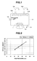
- Photomask blanks having a light-shielding film deposited on a substrate were prepared by the following procedure. Using a DC sputtering apparatus having two targets as shown in FIG. 1 , a light-shielding film composed of silicon and molybdenum was deposited on a quartz substrate. Illustrated in FIG. 1 are a substrate 1, a chamber 101, targets 102a, 102b, a sputtering gas inlet 103, an exhaust port 104, a substrate rotating platform 105, and power supplies 106a, 106b.
- Sputtering gases were introduced at the predetermined flow rates shown in Table 1 so as to establish a gas pressure of 0.05 Pa in the sputtering chamber.
- Two targets were used herein: a Mo target as the transition metal source and a Si (single crystal) target as the silicon source.
- the predetermined discharge powers shown in Table 1 were fed to the respective targets while the substrate was rotated at 30 rpm. In this way, a MoSi film or MoSiON film was deposited to the contents of silicon and molybdenum shown in Table 1 and to the predetermined thickness by controlling the deposition time.
- the contents of light elements in the resultant light-shielding film (as determined by ESCA) are also shown in Table 1.
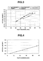
- FIG. 2 plots the film thickness dependency of the optical density of the light-shielding film of Example 1 relative to light of wavelength 248 nm or 193 nm.
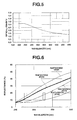
- FIG. 3 plots the film thickness dependency of the optical density of the light-shielding films of Example 1 and Comparative Examples 1 and 2 relative to light of wavelength 193 nm.
- the optical density of metallic Cr film and the film thickness dependency thereof are shown in Table 3 and FIG. 4 , respectively.
- the light-shielding film of Example 1 with a thickness of approximately 40 nm has an optical density of about 3.0 both at the wavelength of 193 nm and 248 nm as seen from FIG. 2 , demonstrating superior light shield to the chromium based light-shielding film (see FIG. 4 ).
- the light-shielding film of Comparative Example 1 with a thickness of approximately 40 nm has an optical density of about 2.5 at the wavelength of 193 nm as seen from FIG. 3 , demonstrating no significant difference in light shield from the metallic chromium light-shielding film (see FIG. 4 ).
- the light-shielding film of Comparative Example 3 has a high sheet resistance, failing to meet electric conductivity.
- Example 2 For the light-shielding film (39 nm thick) of Example 1, the wavelength dependency of its optical density was determined by a spectrophotometer. The results are shown in FIG. 5 . As seen from FIG. 5 , this light-shielding film has an excellent optical density on the short wavelength side, demonstrating light-shielding properties suited for DUV lithography.
- the photomask blank of the invention its light-shielding film has an optical density of around 3 at a thickness of about 40 nm relative to light with a wavelength equal to or less than 248 nm and that the photomask blank of the invention and a photomask obtained therefrom have excellent light-shielding properties as compared with those using a chromium based film as the light-shielding film.
- the light-shielding film can be made thinner, the dry etching time can be reduced accordingly, and an improvement in patterning accuracy due to a thickness reduction of the resist film becomes possible.
- the photomask blank of the invention undergoes minimized pattern size variations even when cleaning steps are repeated.
- Photomask blanks (binary mask blanks) having a light-shielding film and an antireflective film deposited on a substrate were prepared by the following procedure.
- an antireflective film of molybdenum silicide nitride was deposited on the light-shielding film.
- Sputtering gases, Ar gas at a flow rate of 5 sccm, N 2 gas at 50 sccm, and O 2 gas at 0.2 sccm were introduced so as to establish a gas pressure of 0.1 Pa in the sputtering chamber.
- Two targets were used herein: a Mo target as the transition metal source and a Si (single crystal) target as the silicon source.
- Discharge powers of 150 W and 850 W were fed to the Mo and Si targets, respectively, while the substrate was rotated at 30 rpm.
- a MoSiN film was deposited so as to contain silicon and molybdenum in a Si:Mo ratio of 4.5:1 (atomic ratio) and to the thickness shown in Table 4 by controlling the deposition time.
- an antireflective film of chromium oxynitride was deposited on the light-shielding film.
- Sputtering gases, Ar gas at a flow rate of 10 sccm, N 2 , gas at 30 sccm, and O 2 gas at 15 sccm were introduced so as to establish a gas pressure of 0.1 Pa in the sputtering chamber.
- the target used herein was a Cr target. A discharge power of 1,000 W was fed to the Cr target while the substrate was rotated at 30 rpm. In this way, a CrON film was deposited to the thickness shown in Table 4 by controlling the deposition time.
- the optical density (OD) of the light-shielding film was measured by a spectrophotometer, provided that light was incident on the transparent substrate side. The results are shown in Table 5. An optical density of around 3.0 relative to light of wavelength 193 nm is obtained when the antireflective film has a thickness of 23 nm (summing to 48 nm, combined with the light-shielding film).
- the wavelength dependency of reflectance was determined by a spectrophotometer, provided that light was incident on the film surface side.
- the results are shown in Table 5 and FIG. 6 .
- a reflectance of 10 to 20% is obtained at the wavelength 257 nm or 365 nm when the antireflective film has a thickness in the range of 19 to 37 nm, proving a possibility of inspection with a commercially available defect detector.
- a change of reflectance was determined by a spectrophotometer UV-2400PC (Shimadzu Corp.). Under both the conditions, the change of reflectance at wavelength 365 nm was less than 1%, demonstrating the elimination of any practical problems.
- a resist pattern was formed by EB lithography using a chemically amplified resist (film thickness 100 nm).
- a cross-section of the resulting structure was observed under a scanning electron microscope. As a result, the shape of the etched cross-section was satisfactory, demonstrating no significant invasion of the light-shielding film by etching.
- CF 4 80 sccm, 60 W, 2 Pa.
- a halftone phase shift mask blank was fabricated and then processed into a halftone phase shift mask as follows.
- a first layer of 10 nm thick was deposited on a quartz substrate of 6 inch square by a sputtering deposition process, specifically by using a MoZrSi 4 sintered body and a Si single crystal as sputtering targets, feeding a discharge power of 560 W and 1,000 W to the MoZrSi 4 and Si targets, respectively, and rotating the substrate at 30 rpm.
- a gas mixture of 8 sccm of Ar, 20 sccm of N 2 , and 5 sccm of O 2 was introduced as the sputtering gas.
- the gas pressure during sputtering was set at 0.15 Pa.
- a second layer of 40 nm thick as shown in Table 1 was deposited while changing the discharge powers so as to apply 430 W to the MoZrSi 4 target and 1,000 W to the Si target, changing the sputtering gas to a gas mixture of 15 sccm of Ar, 100 sccm of N 2 , and 1 sccm of O 2 , rotating the substrate at 30 rpm, and setting a gas pressure of 0.25 Pa.
- a third layer of 20 nm thick was deposited while changing the discharge powers so as to apply 430 W to the MoZrSi 4 target and 1,000 W to the Si target, changing the sputtering gas to a gas mixture of 5 sccm of Ar, 50 sccm of N 2 , and 1 sccm of O 2 , rotating the substrate at 30 rpm, and setting a gas pressure of 0.1 Pa.
- a halftone phase shift film was obtained in this way.
- a light-shielding film of molybdenum silicide and an antireflective film of molybdenum silicide nitride as in Example 6 were overcoated by the same procedure as in Example 6 to a thickness of 10 nm for the light-shielding film and 20 nm for the antireflective film.
- a resist pattern was formed by EB lithography using a chemically amplified resist (film thickness 250 nm).
- the resist pattern was first stripped by a standard technique, and a negative resist was coated to form a resist film again. Pattern irradiation was carried out to an outer frame portion where a light-shielding pattern was to be left, after which light was irradiated to the entire surface of the substrate being processed from the backside in order to protect the portion of the substrate surface where the halftone pattern had already been etched away.
- the resist film was developed, forming a resist pattern that the resist was left only in the outer frame portion and the portion where the halftone pattern was absent.
- Cl 2 80 sccm, 60 W, 2 Pa.
- a cross section of the mask pattern was observed under a scanning electron microscope, finding a satisfactory etched shape.
- the halftone phase shift film was also found acceptable in phase and transmittance.
- Example 13 By the same procedure as in Example 13, a halftone phase shift film was deposited on a quartz substrate. On this halftone phase shift film, a light-shielding film of molybdenum silicide and an antireflective film of chromium oxynitride as in Example 10 were overcoated by the same procedure as in Example 10 to a thickness of 10 nm for the light-shielding film and 20 nm for the antireflective film. This yielded a halftone phase shift mask blank having a light-shielding film and an antireflective film laminated thereon.
- a resist pattern was formed by EB lithography using a chemically amplified resist (film thickness 100 nm).
- the resist pattern was stripped by a standard technique, and a resist film was formed again.
- a resist pattern was formed so that the resist was left only where a light-shielding pattern was to be left.
- a cross section of the mask pattern was observed under a scanning electron microscope, finding a satisfactory etched shape.
- the halftone phase shift film was also found acceptable in phase and transmittance.
Applications Claiming Priority (2)
| Application Number | Priority Date | Filing Date | Title |
|---|---|---|---|
| JP2004263161A JP4407815B2 (ja) | 2004-09-10 | 2004-09-10 | フォトマスクブランク及びフォトマスク |
| EP05782284A EP1801647B1 (de) | 2004-09-10 | 2005-09-08 | Fotomasken-rohling und fotomaske |
Related Parent Applications (2)
| Application Number | Title | Priority Date | Filing Date |
|---|---|---|---|
| EP05782284.3 Division | 2005-09-08 | ||
| EP05782284A Division EP1801647B1 (de) | 2004-09-10 | 2005-09-08 | Fotomasken-rohling und fotomaske |
Publications (3)
| Publication Number | Publication Date |
|---|---|
| EP2302452A2 true EP2302452A2 (de) | 2011-03-30 |
| EP2302452A3 EP2302452A3 (de) | 2011-05-25 |
| EP2302452B1 EP2302452B1 (de) | 2015-04-01 |
Family
ID=36036449
Family Applications (4)
| Application Number | Title | Priority Date | Filing Date |
|---|---|---|---|
| EP10015810.4A Active EP2302453B1 (de) | 2004-09-10 | 2005-09-08 | Fotomaskenrohling und Fotomaske |
| EP10008135.5A Active EP2246737B1 (de) | 2004-09-10 | 2005-09-08 | Fotomasken-rohling und fotomaske |
| EP10196189.4A Active EP2302452B1 (de) | 2004-09-10 | 2005-09-08 | Fotomaskenrohling und Fotomaske |
| EP05782284A Active EP1801647B1 (de) | 2004-09-10 | 2005-09-08 | Fotomasken-rohling und fotomaske |
Family Applications Before (2)
| Application Number | Title | Priority Date | Filing Date |
|---|---|---|---|
| EP10015810.4A Active EP2302453B1 (de) | 2004-09-10 | 2005-09-08 | Fotomaskenrohling und Fotomaske |
| EP10008135.5A Active EP2246737B1 (de) | 2004-09-10 | 2005-09-08 | Fotomasken-rohling und fotomaske |
Family Applications After (1)
| Application Number | Title | Priority Date | Filing Date |
|---|---|---|---|
| EP05782284A Active EP1801647B1 (de) | 2004-09-10 | 2005-09-08 | Fotomasken-rohling und fotomaske |
Country Status (7)
| Country | Link |
|---|---|
| US (2) | US7691546B2 (de) |
| EP (4) | EP2302453B1 (de) |
| JP (1) | JP4407815B2 (de) |
| KR (1) | KR101165242B1 (de) |
| CN (1) | CN101052917B (de) |
| TW (1) | TW200623233A (de) |
| WO (1) | WO2006028168A1 (de) |
Families Citing this family (74)
| Publication number | Priority date | Publication date | Assignee | Title |
|---|---|---|---|---|
| JP4509050B2 (ja) | 2006-03-10 | 2010-07-21 | 信越化学工業株式会社 | フォトマスクブランク及びフォトマスク |
| JP4883278B2 (ja) | 2006-03-10 | 2012-02-22 | 信越化学工業株式会社 | フォトマスクブランク及びフォトマスクの製造方法 |
| JP4807739B2 (ja) * | 2006-03-30 | 2011-11-02 | Hoya株式会社 | マスクブランク及びフォトマスク |
| JP4919259B2 (ja) * | 2006-03-30 | 2012-04-18 | Hoya株式会社 | マスクブランク及びフォトマスク |
| US7771913B2 (en) * | 2006-04-04 | 2010-08-10 | Shin-Etsu Chemical Co., Ltd. | Resist composition and patterning process using the same |
| JP4737426B2 (ja) * | 2006-04-21 | 2011-08-03 | 信越化学工業株式会社 | フォトマスクブランク |
| JP4842696B2 (ja) * | 2006-04-28 | 2011-12-21 | 信越化学工業株式会社 | フォトマスクブランクの製造方法およびフォトマスクブランク |
| JP5294227B2 (ja) * | 2006-09-15 | 2013-09-18 | Hoya株式会社 | マスクブランク及び転写マスクの製造方法 |
| US20080241745A1 (en) | 2007-03-29 | 2008-10-02 | Fujifilm Corporation | Negative resist composition and pattern forming method using the same |
| JP4958821B2 (ja) * | 2007-03-29 | 2012-06-20 | 富士フイルム株式会社 | ネガ型レジスト組成物及びそれを用いたパターン形成方法 |
| JP5054766B2 (ja) * | 2007-04-27 | 2012-10-24 | Hoya株式会社 | フォトマスクブランク及びフォトマスク |
| JP4466881B2 (ja) | 2007-06-06 | 2010-05-26 | 信越化学工業株式会社 | フォトマスクブランク、レジストパターンの形成方法、及びフォトマスクの製造方法 |
| JP5242110B2 (ja) * | 2007-09-30 | 2013-07-24 | Hoya株式会社 | フォトマスクブランク、フォトマスク及びその製造方法、並びに半導体装置の製造方法 |
| JP4845978B2 (ja) * | 2008-02-27 | 2011-12-28 | Hoya株式会社 | フォトマスクブランクおよびフォトマスク並びにフォトマスクの製造方法 |
| US20090226823A1 (en) * | 2008-03-06 | 2009-09-10 | Micron Technology, Inc. | Reticles including assistant structures, methods of forming such reticles, and methods of utilizing such reticles |
| WO2009123171A1 (ja) * | 2008-03-31 | 2009-10-08 | Hoya株式会社 | フォトマスクブランク、フォトマスクおよびフォトマスクブランクの製造方法 |
| WO2009123172A1 (ja) | 2008-03-31 | 2009-10-08 | Hoya株式会社 | フォトマスクブランク、フォトマスクおよびフォトマスクブランクの製造方法 |
| JP5530075B2 (ja) | 2008-03-31 | 2014-06-25 | Hoya株式会社 | フォトマスクブランク、フォトマスク及びこれらの製造方法 |
| JP5702920B2 (ja) * | 2008-06-25 | 2015-04-15 | Hoya株式会社 | 位相シフトマスクブランク、位相シフトマスクおよび位相シフトマスクブランクの製造方法 |
| JP4849276B2 (ja) * | 2008-08-15 | 2012-01-11 | 信越化学工業株式会社 | グレートーンマスクブランク、グレートーンマスク、及び製品加工標識又は製品情報標識の形成方法 |
| TWI476507B (zh) | 2008-09-30 | 2015-03-11 | Hoya Corp | A mask substrate, a mask, a manufacturing method thereof, and a method of manufacturing the semiconductor element |
| WO2010050447A1 (ja) | 2008-10-29 | 2010-05-06 | Hoya株式会社 | フォトマスクブランク、フォトマスク及びその製造方法 |
| JP5281362B2 (ja) * | 2008-10-31 | 2013-09-04 | Hoya株式会社 | フォトマスクブランク、フォトマスク及びその製造方法 |
| JP4826843B2 (ja) * | 2009-01-15 | 2011-11-30 | 信越化学工業株式会社 | ドライエッチング方法 |
| JP4826842B2 (ja) * | 2009-01-15 | 2011-11-30 | 信越化学工業株式会社 | フォトマスクの製造方法及びフォトマスクブランク |
| CN102365584B (zh) | 2009-01-29 | 2014-07-30 | 迪吉福来克斯有限公司 | 用于在光聚合物表面上产生光掩模的工艺 |
| KR101153663B1 (ko) * | 2009-02-13 | 2012-07-20 | 호야 가부시키가이샤 | 포토마스크 블랭크 및 그 제조 방법과 포토마스크 및 그 제조 방법 |
| WO2010113787A1 (ja) * | 2009-03-31 | 2010-10-07 | Hoya株式会社 | マスクブランク及び転写用マスクの製造方法 |
| WO2010113474A1 (ja) * | 2009-03-31 | 2010-10-07 | Hoya株式会社 | マスクブランクおよび転写用マスク |
| JP5201361B2 (ja) | 2009-05-15 | 2013-06-05 | 信越化学工業株式会社 | フォトマスクブランクの加工方法 |
| JP5257256B2 (ja) * | 2009-06-11 | 2013-08-07 | 信越化学工業株式会社 | フォトマスクの製造方法 |
| JP4739461B2 (ja) | 2009-10-12 | 2011-08-03 | Hoya株式会社 | 転写用マスクの製造方法及び半導体デバイスの製造方法 |
| US8435704B2 (en) * | 2010-03-30 | 2013-05-07 | Hoya Corporation | Mask blank, transfer mask, and methods of manufacturing the same |
| CN102834773B (zh) * | 2010-04-09 | 2016-04-06 | Hoya株式会社 | 相移掩模坯料及其制造方法、以及相移掩模 |
| CN102236247A (zh) * | 2010-05-06 | 2011-11-09 | 中芯国际集成电路制造(上海)有限公司 | 光掩膜的制作方法 |
| JP4697495B2 (ja) * | 2010-05-28 | 2011-06-08 | 信越化学工業株式会社 | フォトマスクブランク及びフォトマスクの製造方法 |
| JP5682493B2 (ja) | 2010-08-04 | 2015-03-11 | 信越化学工業株式会社 | バイナリーフォトマスクブランク及びバイナリーフォトマスクの製造方法 |
| JP5644293B2 (ja) | 2010-09-10 | 2014-12-24 | 信越化学工業株式会社 | 遷移金属ケイ素系材料膜の設計方法 |
| JP5154626B2 (ja) | 2010-09-30 | 2013-02-27 | Hoya株式会社 | マスクブランク、転写用マスク、転写用マスクの製造方法、および半導体デバイスの製造方法 |
| WO2012070209A1 (ja) * | 2010-11-22 | 2012-05-31 | 信越化学工業株式会社 | フォトマスクブランクおよびフォトマスクの製造方法ならびにクロム系材料膜 |
| JP5653888B2 (ja) | 2010-12-17 | 2015-01-14 | Hoya株式会社 | マスクブランク、転写用マスク、転写用マスクの製造方法、及び半導体デバイスの製造方法 |
| JP5920965B2 (ja) | 2011-05-20 | 2016-05-24 | Hoya株式会社 | マスクブランクの製造方法、転写用マスク用の製造方法、および半導体デバイスの製造方法 |
| JP5997530B2 (ja) | 2011-09-07 | 2016-09-28 | Hoya株式会社 | マスクブランク、転写用マスク、および半導体デバイスの製造方法 |
| JP4930737B2 (ja) * | 2011-09-21 | 2012-05-16 | 信越化学工業株式会社 | フォトマスクブランク及びバイナリーマスクの製造方法 |
| JP4930736B2 (ja) * | 2011-09-21 | 2012-05-16 | 信越化学工業株式会社 | フォトマスクの製造方法及びフォトマスク |
| JP6125772B2 (ja) | 2011-09-28 | 2017-05-10 | Hoya株式会社 | 反射型マスクブランク、反射型マスクおよび反射型マスクの製造方法 |
| JP6084391B2 (ja) * | 2011-09-28 | 2017-02-22 | Hoya株式会社 | マスクブランク、転写用マスク、転写用マスクの製造方法および半導体デバイスの製造方法 |
| JP6127977B2 (ja) * | 2011-10-21 | 2017-05-17 | 大日本印刷株式会社 | 大型位相シフトマスクおよび大型位相シフトマスクの製造方法 |
| JP5229838B2 (ja) * | 2011-11-09 | 2013-07-03 | Hoya株式会社 | マスクブランク及びフォトマスク |
| JP5879951B2 (ja) * | 2011-11-21 | 2016-03-08 | 信越化学工業株式会社 | 光パターン照射方法、ハーフトーン位相シフトマスク及びハーフトーン位相シフトマスクブランク |
| JP5896402B2 (ja) | 2011-12-09 | 2016-03-30 | Hoya株式会社 | マスクブランクの製造方法、転写用マスクの製造方法、および半導体デバイスの製造方法 |
| US8703365B2 (en) * | 2012-03-06 | 2014-04-22 | Apple Inc. | UV mask with anti-reflection coating and UV absorption material |
| JP5916447B2 (ja) * | 2012-03-14 | 2016-05-11 | Hoya株式会社 | マスクブランクの製造方法及び転写用マスクの製造方法 |
| JP5739375B2 (ja) | 2012-05-16 | 2015-06-24 | 信越化学工業株式会社 | ハーフトーン位相シフトマスクブランク及びハーフトーン位相シフトマスクの製造方法 |
| JP5795991B2 (ja) | 2012-05-16 | 2015-10-14 | 信越化学工業株式会社 | フォトマスクブランク、フォトマスクの製造方法、および位相シフトマスクの製造方法 |
| JP5795992B2 (ja) | 2012-05-16 | 2015-10-14 | 信越化学工業株式会社 | フォトマスクブランク及びフォトマスクの製造方法 |
| US8823003B2 (en) | 2012-08-10 | 2014-09-02 | Apple Inc. | Gate insulator loss free etch-stop oxide thin film transistor |
| US9601557B2 (en) | 2012-11-16 | 2017-03-21 | Apple Inc. | Flexible display |
| JP5753324B2 (ja) | 2012-11-20 | 2015-07-22 | Hoya株式会社 | マスクブランク、転写用マスク、マスクブランクの製造方法、転写用マスクの製造方法および半導体デバイスの製造方法 |
| JP6394496B2 (ja) | 2014-07-15 | 2018-09-26 | 信越化学工業株式会社 | バイナリフォトマスクブランク、その製造方法、及びバイナリフォトマスクの製造方法 |
| JP6675156B2 (ja) * | 2014-07-30 | 2020-04-01 | 信越化学工業株式会社 | フォトマスクブランクの設計方法 |
| US9600112B2 (en) | 2014-10-10 | 2017-03-21 | Apple Inc. | Signal trace patterns for flexible substrates |
| JP6319059B2 (ja) | 2014-11-25 | 2018-05-09 | 信越化学工業株式会社 | フォトマスクブランク、レジストパターンの形成方法、及びフォトマスクの製造方法 |
| JP6451469B2 (ja) | 2015-04-07 | 2019-01-16 | 信越化学工業株式会社 | フォトマスクブランク、レジストパターン形成方法、及びフォトマスクの製造方法 |
| JP5962811B2 (ja) * | 2015-04-22 | 2016-08-03 | 信越化学工業株式会社 | 光パターン照射方法 |
| JP6341166B2 (ja) * | 2015-09-03 | 2018-06-13 | 信越化学工業株式会社 | フォトマスクブランク |
| JP6451561B2 (ja) * | 2015-09-03 | 2019-01-16 | 信越化学工業株式会社 | フォトマスクブランク |
| JP6398927B2 (ja) * | 2015-09-18 | 2018-10-03 | 信越化学工業株式会社 | フォトマスクブランク、その製造方法及びフォトマスク |
| JP2016095533A (ja) * | 2016-01-25 | 2016-05-26 | 信越化学工業株式会社 | 光パターン照射方法 |
| SG11201807932XA (en) * | 2016-03-29 | 2018-10-30 | Hoya Corp | Mask blank, method for manufacturing mask blank, method for manufacturing transfer mask, and method for manufacturing semiconductor device |
| US10168612B2 (en) | 2016-12-12 | 2019-01-01 | Globalfoundries Inc. | Photomask blank including a thin chromium hardmask |
| KR20180075733A (ko) | 2016-12-26 | 2018-07-05 | 엘지디스플레이 주식회사 | 플렉서블 표시장치 |
| CN109960105A (zh) * | 2017-12-26 | 2019-07-02 | Hoya株式会社 | 光掩模坯料及光掩模的制造方法、显示装置的制造方法 |
| KR102495225B1 (ko) * | 2021-12-15 | 2023-02-06 | 에스케이엔펄스 주식회사 | 블랭크 마스크 및 이를 이용한 포토마스크 |
Citations (9)
| Publication number | Priority date | Publication date | Assignee | Title |
|---|---|---|---|---|
| JPS6385553A (ja) | 1986-09-30 | 1988-04-16 | Toshiba Corp | マスク基板およびマスクパタ−ンの形成方法 |
| JPH01142637A (ja) | 1987-11-30 | 1989-06-05 | Hoya Corp | フォトマスクブランク |
| JPH03116147A (ja) | 1989-09-29 | 1991-05-17 | Hoya Corp | フォトマスクブランクおよびフォトマスク |
| JPH04246649A (ja) | 1991-01-31 | 1992-09-02 | Hoya Corp | フォトマスクブランク及びその製造方法、並びにフォト マスク及びその製造方法 |
| JPH07140635A (ja) | 1992-11-21 | 1995-06-02 | Ulvac Seibaku Kk | 位相シフトマスクおよびその製造方法ならびにその位相シフトマスクを用いた露光方法 |
| JP3093632B2 (ja) | 1996-04-25 | 2000-10-03 | 日本電気アイシーマイコンシステム株式会社 | 半導体記憶装置 |
| JP2001312043A (ja) | 2000-04-27 | 2001-11-09 | Dainippon Printing Co Ltd | ハーフトーン位相シフトフォトマスク及びハーフトーン位相シフトフォトマスク用ブランクス |
| JP2003195479A (ja) | 2001-12-28 | 2003-07-09 | Hoya Corp | ハーフトーン型位相シフトマスクブランク、及びハーフトーン型位相シフトマスクの製造方法 |
| JP2003195483A (ja) | 2001-12-28 | 2003-07-09 | Hoya Corp | フォトマスクブランク、フォトマスク、及びそれらの製造方法 |
Family Cites Families (13)
| Publication number | Priority date | Publication date | Assignee | Title |
|---|---|---|---|---|
| JPS61173253A (ja) | 1985-01-28 | 1986-08-04 | Mitsubishi Electric Corp | フオトマスクブランクの形成方法 |
| JPH0393632A (ja) | 1989-09-04 | 1991-04-18 | Shibason:Kk | 照明灯用レンズの製造方法 |
| JPH0720427Y2 (ja) | 1990-01-11 | 1995-05-15 | 豊生ブレーキ工業株式会社 | シュー間隙自動調節機構を備えたドラムブレーキ |
| JP3032089B2 (ja) | 1992-09-24 | 2000-04-10 | 三菱電機株式会社 | フォトマスク形成方法 |
| JP3116147B2 (ja) | 1992-09-30 | 2000-12-11 | 東芝機械株式会社 | ダイカスト機の給湯方法 |
| US5674647A (en) | 1992-11-21 | 1997-10-07 | Ulvac Coating Corporation | Phase shift mask and manufacturing method thereof and exposure method using phase shift mask |
| US5942356A (en) * | 1996-03-30 | 1999-08-24 | Hoya Corporation | Phase shift mask and phase shift mask blank |
| JP3214840B2 (ja) | 1999-03-08 | 2001-10-02 | ホーヤ株式会社 | 位相シフトマスクの製造方法、及び位相シフトマスクブランクの製造方法 |
| JP2002014458A (ja) | 2000-06-30 | 2002-01-18 | Toppan Printing Co Ltd | ハーフトーン型位相シフトマスクおよびブランク |
| JP2002090977A (ja) | 2000-09-12 | 2002-03-27 | Hoya Corp | 位相シフトマスクブランク、フォトマスクブランク、並びにそれらの製造装置及び製造方法 |
| JP3988041B2 (ja) * | 2002-10-08 | 2007-10-10 | 信越化学工業株式会社 | ハーフトーン位相シフトマスクブランク及びその製造方法 |
| US7005217B2 (en) * | 2003-04-04 | 2006-02-28 | Lsi Logic Corporation | Chromeless phase shift mask |
| JP4246649B2 (ja) | 2004-02-17 | 2009-04-02 | 京セラ株式会社 | 携帯電話機 |
-
2004
- 2004-09-10 JP JP2004263161A patent/JP4407815B2/ja active Active
-
2005
- 2005-09-08 EP EP10015810.4A patent/EP2302453B1/de active Active
- 2005-09-08 WO PCT/JP2005/016511 patent/WO2006028168A1/ja active Application Filing
- 2005-09-08 EP EP10008135.5A patent/EP2246737B1/de active Active
- 2005-09-08 EP EP10196189.4A patent/EP2302452B1/de active Active
- 2005-09-08 EP EP05782284A patent/EP1801647B1/de active Active
- 2005-09-08 KR KR1020077005657A patent/KR101165242B1/ko active IP Right Grant
- 2005-09-08 TW TW094130954A patent/TW200623233A/zh unknown
- 2005-09-08 US US11/662,183 patent/US7691546B2/en active Active
- 2005-09-08 CN CN2005800365654A patent/CN101052917B/zh active Active
-
2010
- 2010-02-19 US US12/709,116 patent/US8007964B2/en active Active
Patent Citations (9)
| Publication number | Priority date | Publication date | Assignee | Title |
|---|---|---|---|---|
| JPS6385553A (ja) | 1986-09-30 | 1988-04-16 | Toshiba Corp | マスク基板およびマスクパタ−ンの形成方法 |
| JPH01142637A (ja) | 1987-11-30 | 1989-06-05 | Hoya Corp | フォトマスクブランク |
| JPH03116147A (ja) | 1989-09-29 | 1991-05-17 | Hoya Corp | フォトマスクブランクおよびフォトマスク |
| JPH04246649A (ja) | 1991-01-31 | 1992-09-02 | Hoya Corp | フォトマスクブランク及びその製造方法、並びにフォト マスク及びその製造方法 |
| JPH07140635A (ja) | 1992-11-21 | 1995-06-02 | Ulvac Seibaku Kk | 位相シフトマスクおよびその製造方法ならびにその位相シフトマスクを用いた露光方法 |
| JP3093632B2 (ja) | 1996-04-25 | 2000-10-03 | 日本電気アイシーマイコンシステム株式会社 | 半導体記憶装置 |
| JP2001312043A (ja) | 2000-04-27 | 2001-11-09 | Dainippon Printing Co Ltd | ハーフトーン位相シフトフォトマスク及びハーフトーン位相シフトフォトマスク用ブランクス |
| JP2003195479A (ja) | 2001-12-28 | 2003-07-09 | Hoya Corp | ハーフトーン型位相シフトマスクブランク、及びハーフトーン型位相シフトマスクの製造方法 |
| JP2003195483A (ja) | 2001-12-28 | 2003-07-09 | Hoya Corp | フォトマスクブランク、フォトマスク、及びそれらの製造方法 |
Also Published As
| Publication number | Publication date |
|---|---|
| EP2302453A3 (de) | 2011-05-25 |
| TW200623233A (en) | 2006-07-01 |
| TWI320579B (de) | 2010-02-11 |
| KR101165242B1 (ko) | 2012-09-13 |
| EP2302452A3 (de) | 2011-05-25 |
| WO2006028168A1 (ja) | 2006-03-16 |
| EP2246737A1 (de) | 2010-11-03 |
| US7691546B2 (en) | 2010-04-06 |
| CN101052917A (zh) | 2007-10-10 |
| US20100143831A1 (en) | 2010-06-10 |
| EP2302452B1 (de) | 2015-04-01 |
| CN101052917B (zh) | 2010-11-03 |
| EP1801647A4 (de) | 2008-01-23 |
| EP1801647B1 (de) | 2011-11-16 |
| JP4407815B2 (ja) | 2010-02-03 |
| KR20070054198A (ko) | 2007-05-28 |
| EP2246737B1 (de) | 2015-12-02 |
| EP2302453A2 (de) | 2011-03-30 |
| JP2006078807A (ja) | 2006-03-23 |
| EP1801647A1 (de) | 2007-06-27 |
| US8007964B2 (en) | 2011-08-30 |
| US20080063950A1 (en) | 2008-03-13 |
| EP2302453B1 (de) | 2015-04-01 |
Similar Documents
| Publication | Publication Date | Title |
|---|---|---|
| EP2302453B1 (de) | Fotomaskenrohling und Fotomaske | |
| EP1936437B1 (de) | Fotomaskenrohling, Fotomaske und Herstellungsverfahren dafür | |
| EP2881790B1 (de) | Fotomaskenrohling | |
| JP5464186B2 (ja) | フォトマスクブランク、フォトマスク及びその製造方法 | |
| CN107870507A (zh) | 半色调相移掩模坯和半色调相移掩模 | |
| US10712654B2 (en) | Photomask blank | |
| EP3373068B1 (de) | Halbtonphasenverschiebungs-fotomaskenrohling | |
| JP2015111246A (ja) | ハーフトーン位相シフト型フォトマスクブランク、ハーフトーン位相シフト型フォトマスク及びパターン露光方法 | |
| JP6287932B2 (ja) | ハーフトーン位相シフト型フォトマスクブランクの製造方法 | |
| EP2261736B1 (de) | Verfahren zur Herstellung einer Photomaske | |
| JP6332109B2 (ja) | ハーフトーン位相シフト型フォトマスクブランクの製造方法 | |
| EP2594992A2 (de) | Beurteilung der Ätzbedingungen für strukturbildende Folien | |
| EP2975459B1 (de) | Rohling einer binären fotomaske, herstellung davon und herstellung einer binären fotomaske | |
| JP2009271562A (ja) | フォトマスクブランクおよびフォトマスクならびにこれらの製造方法 | |
| JP5007843B2 (ja) | フォトマスクブランク及びフォトマスク |
Legal Events
| Date | Code | Title | Description |
|---|---|---|---|
| PUAI | Public reference made under article 153(3) epc to a published international application that has entered the european phase |
Free format text: ORIGINAL CODE: 0009012 |
|
| AC | Divisional application: reference to earlier application |
Ref document number: 1801647 Country of ref document: EP Kind code of ref document: P |
|
| AK | Designated contracting states |
Kind code of ref document: A2 Designated state(s): DE FR GB |
|
| AX | Request for extension of the european patent |
Extension state: AL BA HR MK YU |
|
| PUAL | Search report despatched |
Free format text: ORIGINAL CODE: 0009013 |
|
| AK | Designated contracting states |
Kind code of ref document: A3 Designated state(s): DE FR GB |
|
| AX | Request for extension of the european patent |
Extension state: AL BA HR MK YU |
|
| 17P | Request for examination filed |
Effective date: 20111115 |
|
| REG | Reference to a national code |
Ref country code: DE Ref legal event code: R079 Ref document number: 602005046232 Country of ref document: DE Free format text: PREVIOUS MAIN CLASS: G03F0001080000 Ipc: G03F0001000000 |
|
| GRAP | Despatch of communication of intention to grant a patent |
Free format text: ORIGINAL CODE: EPIDOSNIGR1 |
|
| RIC1 | Information provided on ipc code assigned before grant |
Ipc: G03F 1/00 20120101AFI20141015BHEP |
|
| INTG | Intention to grant announced |
Effective date: 20141028 |
|
| GRAS | Grant fee paid |
Free format text: ORIGINAL CODE: EPIDOSNIGR3 |
|
| GRAA | (expected) grant |
Free format text: ORIGINAL CODE: 0009210 |
|
| AC | Divisional application: reference to earlier application |
Ref document number: 1801647 Country of ref document: EP Kind code of ref document: P |
|
| AK | Designated contracting states |
Kind code of ref document: B1 Designated state(s): DE FR GB |
|
| REG | Reference to a national code |
Ref country code: GB Ref legal event code: FG4D |
|
| REG | Reference to a national code |
Ref country code: DE Ref legal event code: R096 Ref document number: 602005046232 Country of ref document: DE Effective date: 20150513 |
|
| REG | Reference to a national code |
Ref country code: DE Ref legal event code: R097 Ref document number: 602005046232 Country of ref document: DE |
|
| PLBE | No opposition filed within time limit |
Free format text: ORIGINAL CODE: 0009261 |
|
| STAA | Information on the status of an ep patent application or granted ep patent |
Free format text: STATUS: NO OPPOSITION FILED WITHIN TIME LIMIT |
|
| 26N | No opposition filed |
Effective date: 20160105 |
|
| REG | Reference to a national code |
Ref country code: FR Ref legal event code: PLFP Year of fee payment: 12 |
|
| REG | Reference to a national code |
Ref country code: FR Ref legal event code: PLFP Year of fee payment: 13 |
|
| REG | Reference to a national code |
Ref country code: FR Ref legal event code: PLFP Year of fee payment: 14 |
|
| REG | Reference to a national code |
Ref country code: DE Ref legal event code: R081 Ref document number: 602005046232 Country of ref document: DE Owner name: TOPPAN PHOTOMASK CO., LTD., JP Free format text: FORMER OWNERS: SHIN-ETSU CHEMICAL CO., LTD., TOKYO, JP; TOPPAN PRINTING CO., LTD., TOKYO, JP Ref country code: DE Ref legal event code: R081 Ref document number: 602005046232 Country of ref document: DE Owner name: SHIN-ETSU CHEMICAL CO., LTD., JP Free format text: FORMER OWNERS: SHIN-ETSU CHEMICAL CO., LTD., TOKYO, JP; TOPPAN PRINTING CO., LTD., TOKYO, JP |
|
| REG | Reference to a national code |
Ref country code: GB Ref legal event code: 732E Free format text: REGISTERED BETWEEN 20220922 AND 20220928 |
|
| PGFP | Annual fee paid to national office [announced via postgrant information from national office to epo] |
Ref country code: GB Payment date: 20230727 Year of fee payment: 19 |
|
| PGFP | Annual fee paid to national office [announced via postgrant information from national office to epo] |
Ref country code: FR Payment date: 20230808 Year of fee payment: 19 Ref country code: DE Payment date: 20230802 Year of fee payment: 19 |