EP2298543A2 - Mastermodell für eine Linsenanordnung und Herstellungsverfahren dafür - Google Patents
Mastermodell für eine Linsenanordnung und Herstellungsverfahren dafür Download PDFInfo
- Publication number
- EP2298543A2 EP2298543A2 EP10176858A EP10176858A EP2298543A2 EP 2298543 A2 EP2298543 A2 EP 2298543A2 EP 10176858 A EP10176858 A EP 10176858A EP 10176858 A EP10176858 A EP 10176858A EP 2298543 A2 EP2298543 A2 EP 2298543A2
- Authority
- EP
- European Patent Office
- Prior art keywords
- lens
- master model
- lenses
- mold
- portions
- Prior art date
- Legal status (The legal status is an assumption and is not a legal conclusion. Google has not performed a legal analysis and makes no representation as to the accuracy of the status listed.)
- Withdrawn
Links
- 238000004519 manufacturing process Methods 0.000 title claims abstract description 50
- 239000000758 substrate Substances 0.000 claims description 107
- 239000000463 material Substances 0.000 claims description 47
- 238000003384 imaging method Methods 0.000 claims description 41
- 238000000034 method Methods 0.000 claims description 28
- 238000000465 moulding Methods 0.000 claims description 6
- 238000005520 cutting process Methods 0.000 claims description 5
- 238000010276 construction Methods 0.000 abstract description 5
- 239000011347 resin Substances 0.000 description 58
- 229920005989 resin Polymers 0.000 description 58
- 125000006850 spacer group Chemical group 0.000 description 40
- 239000011342 resin composition Substances 0.000 description 26
- 239000000853 adhesive Substances 0.000 description 23
- 230000001070 adhesive effect Effects 0.000 description 23
- 239000012778 molding material Substances 0.000 description 19
- PXHVJJICTQNCMI-UHFFFAOYSA-N nickel Substances [Ni] PXHVJJICTQNCMI-UHFFFAOYSA-N 0.000 description 18
- 238000001723 curing Methods 0.000 description 17
- 239000002245 particle Substances 0.000 description 17
- 230000008569 process Effects 0.000 description 16
- 239000010954 inorganic particle Substances 0.000 description 13
- 238000003491 array Methods 0.000 description 9
- 239000011159 matrix material Substances 0.000 description 9
- 230000003287 optical effect Effects 0.000 description 9
- 230000004308 accommodation Effects 0.000 description 8
- 239000010410 layer Substances 0.000 description 8
- 239000011295 pitch Substances 0.000 description 8
- 229920001187 thermosetting polymer Polymers 0.000 description 8
- 238000010521 absorption reaction Methods 0.000 description 7
- 230000035508 accumulation Effects 0.000 description 6
- 238000009825 accumulation Methods 0.000 description 6
- 239000011521 glass Substances 0.000 description 6
- 229910052759 nickel Inorganic materials 0.000 description 6
- 239000002904 solvent Substances 0.000 description 6
- 239000003795 chemical substances by application Substances 0.000 description 5
- 230000008602 contraction Effects 0.000 description 5
- 238000010438 heat treatment Methods 0.000 description 5
- -1 silica Chemical class 0.000 description 5
- LFQSCWFLJHTTHZ-UHFFFAOYSA-N Ethanol Chemical compound CCO LFQSCWFLJHTTHZ-UHFFFAOYSA-N 0.000 description 4
- UFWIBTONFRDIAS-UHFFFAOYSA-N Naphthalene Chemical compound C1=CC=CC2=CC=CC=C21 UFWIBTONFRDIAS-UHFFFAOYSA-N 0.000 description 4
- 238000006243 chemical reaction Methods 0.000 description 4
- MRELNEQAGSRDBK-UHFFFAOYSA-N lanthanum(3+);oxygen(2-) Chemical compound [O-2].[O-2].[O-2].[La+3].[La+3] MRELNEQAGSRDBK-UHFFFAOYSA-N 0.000 description 4
- 239000000203 mixture Substances 0.000 description 4
- 239000000243 solution Substances 0.000 description 4
- ZWEHNKRNPOVVGH-UHFFFAOYSA-N 2-Butanone Chemical compound CCC(C)=O ZWEHNKRNPOVVGH-UHFFFAOYSA-N 0.000 description 3
- CSCPPACGZOOCGX-UHFFFAOYSA-N Acetone Chemical compound CC(C)=O CSCPPACGZOOCGX-UHFFFAOYSA-N 0.000 description 3
- UHOVQNZJYSORNB-UHFFFAOYSA-N Benzene Chemical compound C1=CC=CC=C1 UHOVQNZJYSORNB-UHFFFAOYSA-N 0.000 description 3
- XEKOWRVHYACXOJ-UHFFFAOYSA-N Ethyl acetate Chemical compound CCOC(C)=O XEKOWRVHYACXOJ-UHFFFAOYSA-N 0.000 description 3
- LYCAIKOWRPUZTN-UHFFFAOYSA-N Ethylene glycol Chemical compound OCCO LYCAIKOWRPUZTN-UHFFFAOYSA-N 0.000 description 3
- KFZMGEQAYNKOFK-UHFFFAOYSA-N Isopropanol Chemical compound CC(C)O KFZMGEQAYNKOFK-UHFFFAOYSA-N 0.000 description 3
- OKKJLVBELUTLKV-UHFFFAOYSA-N Methanol Chemical compound OC OKKJLVBELUTLKV-UHFFFAOYSA-N 0.000 description 3
- VYPSYNLAJGMNEJ-UHFFFAOYSA-N Silicium dioxide Chemical compound O=[Si]=O VYPSYNLAJGMNEJ-UHFFFAOYSA-N 0.000 description 3
- YXFVVABEGXRONW-UHFFFAOYSA-N Toluene Chemical compound CC1=CC=CC=C1 YXFVVABEGXRONW-UHFFFAOYSA-N 0.000 description 3
- 125000001931 aliphatic group Chemical group 0.000 description 3
- 239000000178 monomer Substances 0.000 description 3
- RVTZCBVAJQQJTK-UHFFFAOYSA-N oxygen(2-);zirconium(4+) Chemical compound [O-2].[O-2].[Zr+4] RVTZCBVAJQQJTK-UHFFFAOYSA-N 0.000 description 3
- 230000009467 reduction Effects 0.000 description 3
- 239000004065 semiconductor Substances 0.000 description 3
- 229910001928 zirconium oxide Inorganic materials 0.000 description 3
- XDTMQSROBMDMFD-UHFFFAOYSA-N Cyclohexane Chemical compound C1CCCCC1 XDTMQSROBMDMFD-UHFFFAOYSA-N 0.000 description 2
- WYURNTSHIVDZCO-UHFFFAOYSA-N Tetrahydrofuran Chemical compound C1CCOC1 WYURNTSHIVDZCO-UHFFFAOYSA-N 0.000 description 2
- GWEVSGVZZGPLCZ-UHFFFAOYSA-N Titan oxide Chemical compound O=[Ti]=O GWEVSGVZZGPLCZ-UHFFFAOYSA-N 0.000 description 2
- 238000003848 UV Light-Curing Methods 0.000 description 2
- XLOMVQKBTHCTTD-UHFFFAOYSA-N Zinc monoxide Chemical compound [Zn]=O XLOMVQKBTHCTTD-UHFFFAOYSA-N 0.000 description 2
- 230000004913 activation Effects 0.000 description 2
- ORILYTVJVMAKLC-UHFFFAOYSA-N adamantane Chemical compound C1C(C2)CC3CC1CC2C3 ORILYTVJVMAKLC-UHFFFAOYSA-N 0.000 description 2
- 229910001573 adamantine Inorganic materials 0.000 description 2
- 125000003118 aryl group Chemical group 0.000 description 2
- IOJUPLGTWVMSFF-UHFFFAOYSA-N benzothiazole Chemical compound C1=CC=C2SC=NC2=C1 IOJUPLGTWVMSFF-UHFFFAOYSA-N 0.000 description 2
- 230000005540 biological transmission Effects 0.000 description 2
- 239000003054 catalyst Substances 0.000 description 2
- 239000002270 dispersing agent Substances 0.000 description 2
- 230000005684 electric field Effects 0.000 description 2
- 238000009713 electroplating Methods 0.000 description 2
- 125000000524 functional group Chemical group 0.000 description 2
- 239000003999 initiator Substances 0.000 description 2
- 238000001746 injection moulding Methods 0.000 description 2
- HJOVHMDZYOCNQW-UHFFFAOYSA-N isophorone Chemical compound CC1=CC(=O)CC(C)(C)C1 HJOVHMDZYOCNQW-UHFFFAOYSA-N 0.000 description 2
- 238000010030 laminating Methods 0.000 description 2
- 238000003475 lamination Methods 0.000 description 2
- 229910052751 metal Inorganic materials 0.000 description 2
- 239000002184 metal Substances 0.000 description 2
- 229910044991 metal oxide Inorganic materials 0.000 description 2
- 150000004706 metal oxides Chemical class 0.000 description 2
- UMRZSTCPUPJPOJ-KNVOCYPGSA-N norbornane Chemical compound C1C[C@H]2CC[C@@H]1C2 UMRZSTCPUPJPOJ-KNVOCYPGSA-N 0.000 description 2
- 150000007524 organic acids Chemical class 0.000 description 2
- TWNQGVIAIRXVLR-UHFFFAOYSA-N oxo(oxoalumanyloxy)alumane Chemical compound O=[Al]O[Al]=O TWNQGVIAIRXVLR-UHFFFAOYSA-N 0.000 description 2
- 238000007747 plating Methods 0.000 description 2
- 238000007142 ring opening reaction Methods 0.000 description 2
- 238000007789 sealing Methods 0.000 description 2
- 229910052710 silicon Inorganic materials 0.000 description 2
- 239000010703 silicon Substances 0.000 description 2
- 229910000679 solder Inorganic materials 0.000 description 2
- 239000000126 substance Substances 0.000 description 2
- XOLBLPGZBRYERU-UHFFFAOYSA-N tin dioxide Chemical compound O=[Sn]=O XOLBLPGZBRYERU-UHFFFAOYSA-N 0.000 description 2
- 229910001887 tin oxide Inorganic materials 0.000 description 2
- OGIDPMRJRNCKJF-UHFFFAOYSA-N titanium oxide Inorganic materials [Ti]=O OGIDPMRJRNCKJF-UHFFFAOYSA-N 0.000 description 2
- 239000012780 transparent material Substances 0.000 description 2
- RYHBNJHYFVUHQT-UHFFFAOYSA-N 1,4-Dioxane Chemical compound C1COCCO1 RYHBNJHYFVUHQT-UHFFFAOYSA-N 0.000 description 1
- OPELWUSJOIBVJS-UHFFFAOYSA-N 3,3'-spirobi[1,2-dihydroindene] Chemical compound C12=CC=CC=C2CCC11C2=CC=CC=C2CC1 OPELWUSJOIBVJS-UHFFFAOYSA-N 0.000 description 1
- DKPFZGUDAPQIHT-UHFFFAOYSA-N Butyl acetate Natural products CCCCOC(C)=O DKPFZGUDAPQIHT-UHFFFAOYSA-N 0.000 description 1
- PXGOKWXKJXAPGV-UHFFFAOYSA-N Fluorine Chemical compound FF PXGOKWXKJXAPGV-UHFFFAOYSA-N 0.000 description 1
- NTIZESTWPVYFNL-UHFFFAOYSA-N Methyl isobutyl ketone Chemical compound CC(C)CC(C)=O NTIZESTWPVYFNL-UHFFFAOYSA-N 0.000 description 1
- UIHCLUNTQKBZGK-UHFFFAOYSA-N Methyl isobutyl ketone Natural products CCC(C)C(C)=O UIHCLUNTQKBZGK-UHFFFAOYSA-N 0.000 description 1
- CTQNGGLPUBDAKN-UHFFFAOYSA-N O-Xylene Chemical compound CC1=CC=CC=C1C CTQNGGLPUBDAKN-UHFFFAOYSA-N 0.000 description 1
- ISWSIDIOOBJBQZ-UHFFFAOYSA-N Phenol Chemical compound OC1=CC=CC=C1 ISWSIDIOOBJBQZ-UHFFFAOYSA-N 0.000 description 1
- 239000006087 Silane Coupling Agent Substances 0.000 description 1
- UCKMPCXJQFINFW-UHFFFAOYSA-N Sulphide Chemical compound [S-2] UCKMPCXJQFINFW-UHFFFAOYSA-N 0.000 description 1
- RTAQQCXQSZGOHL-UHFFFAOYSA-N Titanium Chemical compound [Ti] RTAQQCXQSZGOHL-UHFFFAOYSA-N 0.000 description 1
- 238000002441 X-ray diffraction Methods 0.000 description 1
- HCHKCACWOHOZIP-UHFFFAOYSA-N Zinc Chemical compound [Zn] HCHKCACWOHOZIP-UHFFFAOYSA-N 0.000 description 1
- 239000000654 additive Substances 0.000 description 1
- 125000000217 alkyl group Chemical group 0.000 description 1
- PNEYBMLMFCGWSK-UHFFFAOYSA-N aluminium oxide Inorganic materials [O-2].[O-2].[O-2].[Al+3].[Al+3] PNEYBMLMFCGWSK-UHFFFAOYSA-N 0.000 description 1
- 239000003963 antioxidant agent Substances 0.000 description 1
- 150000004945 aromatic hydrocarbons Chemical class 0.000 description 1
- QRUDEWIWKLJBPS-UHFFFAOYSA-N benzotriazole Chemical compound C1=CC=C2N[N][N]C2=C1 QRUDEWIWKLJBPS-UHFFFAOYSA-N 0.000 description 1
- 239000012964 benzotriazole Substances 0.000 description 1
- 229920001400 block copolymer Polymers 0.000 description 1
- 238000007664 blowing Methods 0.000 description 1
- 125000005587 carbonate group Chemical group 0.000 description 1
- 150000001735 carboxylic acids Chemical class 0.000 description 1
- 238000005266 casting Methods 0.000 description 1
- 229910000420 cerium oxide Inorganic materials 0.000 description 1
- 230000000295 complement effect Effects 0.000 description 1
- 239000002131 composite material Substances 0.000 description 1
- 150000001875 compounds Chemical class 0.000 description 1
- 239000007822 coupling agent Substances 0.000 description 1
- 239000003085 diluting agent Substances 0.000 description 1
- 238000009826 distribution Methods 0.000 description 1
- 238000001035 drying Methods 0.000 description 1
- 239000000428 dust Substances 0.000 description 1
- 230000000694 effects Effects 0.000 description 1
- 125000003700 epoxy group Chemical group 0.000 description 1
- 150000002148 esters Chemical class 0.000 description 1
- 238000005530 etching Methods 0.000 description 1
- 150000002170 ethers Chemical class 0.000 description 1
- 150000002221 fluorine Chemical class 0.000 description 1
- 229910052731 fluorine Inorganic materials 0.000 description 1
- 239000011737 fluorine Substances 0.000 description 1
- 230000009477 glass transition Effects 0.000 description 1
- FUZZWVXGSFPDMH-UHFFFAOYSA-N hexanoic acid Chemical compound CCCCCC(O)=O FUZZWVXGSFPDMH-UHFFFAOYSA-N 0.000 description 1
- 230000002209 hydrophobic effect Effects 0.000 description 1
- 238000006459 hydrosilylation reaction Methods 0.000 description 1
- 239000012535 impurity Substances 0.000 description 1
- 150000002500 ions Chemical class 0.000 description 1
- 230000001678 irradiating effect Effects 0.000 description 1
- 150000002576 ketones Chemical class 0.000 description 1
- 239000007788 liquid Substances 0.000 description 1
- 150000002739 metals Chemical class 0.000 description 1
- 230000004048 modification Effects 0.000 description 1
- 238000012986 modification Methods 0.000 description 1
- 238000009740 moulding (composite fabrication) Methods 0.000 description 1
- 229910000484 niobium oxide Inorganic materials 0.000 description 1
- URLJKFSTXLNXLG-UHFFFAOYSA-N niobium(5+);oxygen(2-) Chemical compound [O-2].[O-2].[O-2].[O-2].[O-2].[Nb+5].[Nb+5] URLJKFSTXLNXLG-UHFFFAOYSA-N 0.000 description 1
- 239000003921 oil Substances 0.000 description 1
- 238000005457 optimization Methods 0.000 description 1
- 235000005985 organic acids Nutrition 0.000 description 1
- 239000011146 organic particle Substances 0.000 description 1
- 125000003566 oxetanyl group Chemical group 0.000 description 1
- BMMGVYCKOGBVEV-UHFFFAOYSA-N oxo(oxoceriooxy)cerium Chemical compound [Ce]=O.O=[Ce]=O BMMGVYCKOGBVEV-UHFFFAOYSA-N 0.000 description 1
- SIWVEOZUMHYXCS-UHFFFAOYSA-N oxo(oxoyttriooxy)yttrium Chemical compound O=[Y]O[Y]=O SIWVEOZUMHYXCS-UHFFFAOYSA-N 0.000 description 1
- 150000003009 phosphonic acids Chemical class 0.000 description 1
- 235000011007 phosphoric acid Nutrition 0.000 description 1
- 150000003016 phosphoric acids Chemical class 0.000 description 1
- 230000001699 photocatalysis Effects 0.000 description 1
- 238000000206 photolithography Methods 0.000 description 1
- 229920000642 polymer Polymers 0.000 description 1
- 238000006116 polymerization reaction Methods 0.000 description 1
- 238000003825 pressing Methods 0.000 description 1
- 238000010526 radical polymerization reaction Methods 0.000 description 1
- 230000009257 reactivity Effects 0.000 description 1
- 239000004576 sand Substances 0.000 description 1
- 150000003346 selenoethers Chemical class 0.000 description 1
- 239000000377 silicon dioxide Substances 0.000 description 1
- 239000007787 solid Substances 0.000 description 1
- 125000003003 spiro group Chemical group 0.000 description 1
- 150000003460 sulfonic acids Chemical class 0.000 description 1
- 239000002344 surface layer Substances 0.000 description 1
- XSOKHXFFCGXDJZ-UHFFFAOYSA-N telluride(2-) Chemical compound [Te-2] XSOKHXFFCGXDJZ-UHFFFAOYSA-N 0.000 description 1
- YLQBMQCUIZJEEH-UHFFFAOYSA-N tetrahydrofuran Natural products C=1C=COC=1 YLQBMQCUIZJEEH-UHFFFAOYSA-N 0.000 description 1
- 150000003573 thiols Chemical class 0.000 description 1
- XLYOFNOQVPJJNP-UHFFFAOYSA-N water Substances O XLYOFNOQVPJJNP-UHFFFAOYSA-N 0.000 description 1
- 239000008096 xylene Substances 0.000 description 1
- 229910052725 zinc Inorganic materials 0.000 description 1
- 239000011701 zinc Substances 0.000 description 1
- 239000011787 zinc oxide Substances 0.000 description 1
Images


Classifications
-
- B—PERFORMING OPERATIONS; TRANSPORTING
- B29—WORKING OF PLASTICS; WORKING OF SUBSTANCES IN A PLASTIC STATE IN GENERAL
- B29D—PRODUCING PARTICULAR ARTICLES FROM PLASTICS OR FROM SUBSTANCES IN A PLASTIC STATE
- B29D11/00—Producing optical elements, e.g. lenses or prisms
- B29D11/00009—Production of simple or compound lenses
- B29D11/00278—Lenticular sheets
-
- B—PERFORMING OPERATIONS; TRANSPORTING
- B29—WORKING OF PLASTICS; WORKING OF SUBSTANCES IN A PLASTIC STATE IN GENERAL
- B29C—SHAPING OR JOINING OF PLASTICS; SHAPING OF MATERIAL IN A PLASTIC STATE, NOT OTHERWISE PROVIDED FOR; AFTER-TREATMENT OF THE SHAPED PRODUCTS, e.g. REPAIRING
- B29C33/00—Moulds or cores; Details thereof or accessories therefor
- B29C33/38—Moulds or cores; Details thereof or accessories therefor characterised by the material or the manufacturing process
- B29C33/3842—Manufacturing moulds, e.g. shaping the mould surface by machining
- B29C33/3857—Manufacturing moulds, e.g. shaping the mould surface by machining by making impressions of one or more parts of models, e.g. shaped articles and including possible subsequent assembly of the parts
- B29C33/3878—Manufacturing moulds, e.g. shaping the mould surface by machining by making impressions of one or more parts of models, e.g. shaped articles and including possible subsequent assembly of the parts used as masters for making successive impressions
-
- B—PERFORMING OPERATIONS; TRANSPORTING
- B29—WORKING OF PLASTICS; WORKING OF SUBSTANCES IN A PLASTIC STATE IN GENERAL
- B29D—PRODUCING PARTICULAR ARTICLES FROM PLASTICS OR FROM SUBSTANCES IN A PLASTIC STATE
- B29D11/00—Producing optical elements, e.g. lenses or prisms
- B29D11/00009—Production of simple or compound lenses
- B29D11/00278—Lenticular sheets
- B29D11/00307—Producing lens wafers
-
- B—PERFORMING OPERATIONS; TRANSPORTING
- B29—WORKING OF PLASTICS; WORKING OF SUBSTANCES IN A PLASTIC STATE IN GENERAL
- B29D—PRODUCING PARTICULAR ARTICLES FROM PLASTICS OR FROM SUBSTANCES IN A PLASTIC STATE
- B29D11/00—Producing optical elements, e.g. lenses or prisms
- B29D11/00009—Production of simple or compound lenses
- B29D11/0048—Moulds for lenses
- B29D11/0049—Double sided moulds
-
- B—PERFORMING OPERATIONS; TRANSPORTING
- B29—WORKING OF PLASTICS; WORKING OF SUBSTANCES IN A PLASTIC STATE IN GENERAL
- B29C—SHAPING OR JOINING OF PLASTICS; SHAPING OF MATERIAL IN A PLASTIC STATE, NOT OTHERWISE PROVIDED FOR; AFTER-TREATMENT OF THE SHAPED PRODUCTS, e.g. REPAIRING
- B29C43/00—Compression moulding, i.e. applying external pressure to flow the moulding material; Apparatus therefor
- B29C43/02—Compression moulding, i.e. applying external pressure to flow the moulding material; Apparatus therefor of articles of definite length, i.e. discrete articles
- B29C43/021—Compression moulding, i.e. applying external pressure to flow the moulding material; Apparatus therefor of articles of definite length, i.e. discrete articles characterised by the shape of the surface
Definitions
- the present invention relates to a master model of a lens array and a method of manufacturing the same.
- imaging units are generally provided with a solid-state imaging device such as a CCD (Charge Coupled Device) image sensor, a CMOS (Complementary Metal-Oxide Semiconductor) image sensor, or the like, and a lens for forming an image on a light sensing surface of the solid-state imaging device.
- CCD Charge Coupled Device
- CMOS Complementary Metal-Oxide Semiconductor
- a method of mass-producing imaging units whereby a sensor array in which a plurality of solid-state imaging devices is arranged and a lens array in which a plurality of lens portions is arranged in the same manner are made to overlap each other, are combined into a single body and then the lens array and the sensor array are cut so that they include the lens portions and the solid-state imaging devices, respectively.
- curved surfaces formed in the shape of predetermined lens surfaces are arranged on one surface and the other surface of the master model, respectively.
- a lens forming surface which is in an inverse shape of the curved surface in the shape of the lens surface that is arranged on one surface of the master model, is arranged
- a lens forming surface which is in an inverse shape of the curved surface in the shape of the lens surface that is arranged on the other surface of the master model, is arranged.
- lens portions are formed between the lens forming surfaces which are composed of a pair of the upper mold and the lower mold, and these lens portions are connected together by a substrate portion formed between the forming surfaces except for the lens forming surfaces of the upper mold and the lower mold.
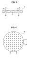
- a wafer in the shape of a circular plate has a diameter of 6 inches, 8 inches, or 12 inches, as a whole, and for example, thousands of lens portions are arranged on the wafer.
- a lens array in particular is called a wafer-level lens array.
- a master model of a lens array in the method of manufacturing a lens array, it is necessary to repeat the process of transferring the lens forming surfaces of molds to resin supplied onto one surface and the other surface of the substrate and curing the supplied resin for as many times as the number of lens portions arranged on the lens array.
- manufacturing the master model takes a very long time.
- resin since resin is supplied to and formed on the substrate, a manufacturing apparatus becomes larger-scaled due to the employment of resin supply means, mold driving means, measures taken to prevent leakage of supplied resin, and the like.
- a plurality of members corresponding to lenses is arranged and connected, and thus the master model of the lens array can be manufactured in a relatively short time using an apparatus with a simpler construction in comparison to repeating of a process of transferring lens forming surfaces of molds to resin on the substrate and curing the resin.
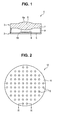
- an imaging unit 1 includes a sensor module 2 and a lens module 3.
- the sensor module 2 includes a solid-state imaging device 4 and a substrate portion 5.
- the substrate portion 5, for example, is formed of a semiconductor material such as silicon.
- the solid-state image device 4, for example, may be a CCD image sensor, a CMOS image sensor, or the like, and is configured by forming a light sensing region, an insulating layer, an electrode, a wire, and the like, on the substrate portion 5 through repetition of known processes of layer forming, photolithography, etching, impurity addition, and the like, with respect to the substrate portion 5.
- the lens module 3 includes a lens portion 6 and a flange portion 7.
- the lens portion 6 has predetermined lens surfaces 6a and 6b formed on one surface and the other surface thereof. Although the both lens surfaces 6a and 6b are illustrated as convex-shaped spherical surfaces, diverse combinations of a convex-shaped spherical surface, a concave-shaped spherical surface, a non-spherical surface, and a plane may be adopted according to their uses.
- the flange portion 7 is projected from the circumference of the lens portion 6 to surround the circumference of the lens portion 6.
- the lens portion 6 and the flange portion 7 are formed of a transparent material in a body.
- the lens module 3 is laminated on the sensor module 2 through spacers 9 between the flange portion 7 and the substrate portion 5 and is attached to the sensor module 2.
- the spacers 9 are formed with a thickness that corresponds to a predetermined distance between the substrate portion 5 of the sensor module 2 and the flange portion 7 of the lens module 3 so that the lens portion 6 of the lens module 3 forms an image on the light sensing surface of the solid-state imaging device 4 of the sensor module 2.
- the spacers 9 and the modules 2 and 3 are bonded, for example, using adhesives or the like.
- the shape of the spacers 9, which are formed with a thickness that corresponds to a predetermined distance between the substrate portion 5 of the sensor module 2 and the flange portion 7 of the lens module 3, is not specifically limited, but it is preferable that the spacers 9 are frame-shaped members that surround the periphery of the solid-state imaging device 4 and separate the modules 2 and 3 from each other on the outside of the modules. According to this configuration, foreign substances such as dust are prevented from entering into the space between the modules 2 and 3 and being attached to the light sensing surface of the solid-state imaging device 4. Further, by forming the spacers 9 with a shading material, unnecessary light that is incident from the space between the modules 2 and 3 to the solid-state imaging device 4 can be intercepted.
- one lens module 3 is attached to the sensor module 2.
- a plurality of lens modules 3 may be attached to the sensor module 2.
- the plurality of lens modules 3 is sequentially laminated through the intervention of spacers that are equivalent to the spacers 9, and is attached to the sensor module 2.
- the lens surfaces 6a and 6b of the lens portion 6 may differ according to lens modules 3.
- the imaging unit 1 as configured above is reflow-packaged on a circuit board of a portable terminal and so on. On a position of the circuit board where the imaging unit 1 is packaged, solder paste is pre-printed, and the imaging unit 1 is placed thereon. Then, a heating process, such as irradiation of infrared rays onto the circuit board including the imaging unit 1 or hot wind blowing thereto is performed. Through this heating process, the solder is melted and the imaging unit 1 is packaged on the circuit board.
- the lens module 3 is obtained by cutting the lens array in which a plurality of lens portions 6 is one-dimensionally or two-dimensionally arranged so that the lens module includes the lens portion 6. Also, in the same manner, the sensor module 2 is obtained by cutting the lens array in which a plurality of solid-state imaging devices is one-dimensionally or two-dimensionally arranged so that the sensor module includes the solid-state imaging device.
- the lens array for obtaining the lens modules 3 will be described in detail.
- the lens array 10 as illustrated in Figs. 2 and 3 includes a plurality of lens portions 6, and a substrate portion 11 that connects the lens portions 6 together.
- This lens array 10 is a wafer-level lens array which is in the form of a wafer of a predetermined size as a whole and on which the plurality of lens portions 6 is arranged.
- the plurality of lens portions 6 is two-dimensionally arranged.
- the lens portions 6 and the substrate portion 11 are formed of a transparent material in a body.
- the lens module 3 (see Fig. 1 ) is obtained by cutting the substrate portion 11 between neighboring lens portions 6 in the wafer-level lens array 10. The cut portion of the substrate portion 11 which belongs to each lens portion 6 becomes the flange portion 7 of the lens module 3.
- a master model of the wafer-level lens array 10 is manufactured and a mold is manufactured from the master model. Then, the wafer-level lens array 10 is manufactured using the mold.
- a master model of the wafer-level lens array 10 and a method of manufacturing the same will be described.
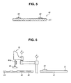
- a master model 40 as illustrated in Figs. 4 and 5 includes a substrate 41 and a plurality of members 42 corresponding to lenses.
- the members 42 corresponding to lenses are arranged on the substrate 41 and are adhesively fixed to the substrate 41.
- the members 42 corresponding to lenses are two-dimensionally arranged to correspond to the arrangement of the plurality of lens portions 6 in the wafer-level lens array 10.
- the substrate 41 is in the form of a wafer having the same size as that of the wafer-level lens array 10.
- the material of the substrate 41 is not specially limited, but, for example, may be glass or resin.
- the member 42 corresponding to a lens has a curved surface which is in the same shape as that of a lens surface 6a on the surface side that is formed on the lens portion 6 of the wafer-level lens array 10, and the other surface of the member 42 is in a plane shape.
- the member 42 corresponding to a lens is formed by a glass press molding or a resin injection molding that is generally performed in manufacturing lenses for a digital camera.
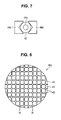
- Fig. 6 is a view illustrating a method of manufacturing a master model 40.
- a plurality of members 42 corresponding to lenses is pre-produced, and the produced members 42 corresponding to lenses are aligned and received in a lens holder 43.
- adhesives 51 are spread.
- the adhesives for example, a photocurable or thermosetting resin material is used.
- an XY robot 44 that can precisely scan on the substrate 41, the members 42 corresponding to lenses received in the lens holder 43 are maintained, and the members 42 corresponding to lenses are extracted one by one from the lens holder 43 to be transported onto the substrate 41.
- the members 42 corresponding to lenses are positioned to be arranged on predetermined positions of the substrate 41, and are closely adhered to the surface of the substrate 41 by pressing the members 42 corresponding to lenses onto the substrate 41.
- the holding of the members 42 corresponding to lenses by the XY robot 44 is performed using an absorption pad.
- the member 42 corresponding to a lens is inserted between a pair of V-shaped blocks 44b that is driven to be opened or closed to perform the centering of support portion 44a of the XY robot 44 on the member 42 corresponding to a lens.
- the centering of the support portion 44a of the XY robot 44 on the member 42 corresponding to a lens may be performed using other appropriate guide means.
- the members 42 corresponding to lenses are arranged on the substrate 41.
- the members 42 corresponding to lenses are irradiated with UV rays, while in the case where thermosetting resin is used as the adhesives 51, the adhesives 51 are heated and then is cured to fix the members 42 corresponding to lenses to the substrate 41.
- a master model 40 having the same shape as the surface of the wafer-level lens array 10 is manufactured.
- the master model 40 can be manufactured in a relatively short time with simple construction of the apparatus in comparison to the case where a process of transferring resin onto the lens forming surface of the mold and curing the resin on the substrate is repeated.
- a master model on the other surface of the wafer-level lens array 10 is manufactured by arranging a plurality of members corresponding to lenses having curved surfaces in the same shape as the lens surface 6b on the other surface side, which are formed on the lens portions 6 of the wafer-level lens array 10, and fixing the members corresponding to lenses to the substrate.
- the master model of the surface shape of the wafer-level lens array 10 and the master model of the other surface shape of the wafer-level lens array 10 are dividedly manufactured.
- the respective members corresponding to lenses may be fixed to one surface and the other surface of a shared substrate.
- the members 42 corresponding to lenses are extracted one by one from the lens holder 43 to be transported onto the substrate 41.
- a plurality of support portions 44a may be provided on the XY robot 44, and plural members 42 corresponding to lenses may be extracted from the lens holder 43 at a time to be arranged on the substrate 41.
- the position of one of the plurality of members 42 corresponding to lenses is determined on the substrate 41 in a state where the plurality of members 42 corresponding to lenses have been made in a connection state with each other by pitch in a line on the substrate 41, other members 42 corresponding to lenses are arranged in predetermined positions by themselves on the substrate 41, and thus the work efficiency is improved.
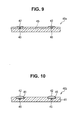
- a master model 40a as shown in Figs. 8 and 9 includes a substrate 41 and a plurality of members 42 corresponding to lenses. Also, on the surface of the substrate 41, a plurality of concave portions 45 is formed. The concave portions 45 are installed on places where the members 42 corresponding to lenses are arranged. In an illustrated example, the concave portions 45 are connected to the neighboring concave portions 45 along rows or columns of the members 42 corresponding to lenses arranged in the form of a matrix. Since the concave portions 45 are connected along the rows or columns, they form lattice-shaped grooves. The concave portions 45 are filled with adhesives, and the members 42 corresponding to lenses are adhesively fixed to the substrate 41 by the adhesives filled into the concave portions 45.
- the surface of the substrate 41 is not covered with the adhesives, and the close contact of the members 42 corresponding to lenses with the surface of the substrate 41 is performed more accurately.
- the center axes of the members 42 corresponding to lenses (which correspond to optical exes of the lens portions 6) are prevented from falling down.
- the filling of adhesives into all the concave portions 45 is facilitated in comparison to a case where the concave portions 45 are independently provided.
- the concave portions 45 are connected along the rows or columns to form lattice-shaped grooves, the positions of the members 42 corresponding to lenses on the substrate 41 can be determined considering the lattice points as indexes.
- a master model 40b as illustrated in Fig. 10 includes a substrate 41 and a plurality of members 42 corresponding to lenses. Also, on the surface of the substrate 41, a plurality of interlocking concave portions 46 is formed.
- the interlocking concave portions 46 are installed on places where the members 42 corresponding to lenses are arranged, and are formed with a size enough to accommodate the member 42 corresponding to a lens inserted therein. According to this, the position determination of the members 42 corresponding to lenses is facilitated, and the position determination accuracy can be improved.
- the interlocking concave portions 46 may be formed by performing a sand blast process with respect to the substrate 41 using a mask that exposes the places that form the interlocking concave portions 46. In this case, in the illustrated example, the concave portions 45 into which the adhesives are filled are installed on the bottom surfaces of the interlocking concave portions 46.
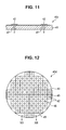
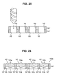
- the master model 40c as illustrated in Fig. 11 includes a substrate 41 and a plurality of members 42 corresponding to lenses.
- a plurality of absorption holes 47 is formed in the substrate 41.
- the absorption holes 47 penetrate the substrate 41 in the thickness direction of the substrate 41, and are open at places where the members 42 corresponding to lenses are arranged.
- the members 42 corresponding to lenses are absorbed to the substrate 41 by decompressing the absorption holes 47, and in this state, the members 42 corresponding to lenses are fixed to the substrate 41 by sealing the absorption holes 47.
- the surface of the substrate 41 is not covered with the adhesives, and the members 42 corresponding to lenses and the surface of the substrate 41 become in close contact with each other to prevent the center axes of the members 42 corresponding to lenses from falling down.
- the members 42 corresponding to lenses may also be fixed by making the adhesives flow into the circumference of the members 42 corresponding to lenses and curing the adhesives in a state where the members 42 corresponding to lenses are absorbed to the substrate 41.
- the master model 40d as illustrated in Figs. 12 and 13 includes a substrate 41 and a plurality of members 42 corresponding to lenses. Also, flange portions 48 are installed around the members 42 corresponding to lenses. The flange portions 48 are formed to be filled between the neighboring members 42 corresponding to lenses when the members 42 corresponding to lenses are arranged on the substrate 41, and in the illustrated example, the flange portions 48 are in the shape of tetragons as seen in the plan view. Accordingly, the position of one member 42 corresponding to a lens is determined on the substrate 41, and other members 42 corresponding to lenses are arranged on predetermined positions of the substrate 41 by contacting side surfaces of the flange portions 48, respectively, thereby improving the work efficiency.
- putties 49 composed of the same material as that of the members 42 corresponding to lenses, such as glass, resin, or the like, are filled up to the same height as that of the neighboring flange portions 48.
- the plurality of members 42 corresponding to lenses is fixed to the substrate 41 and is connected together through the substrate 41.
- the members 42 corresponding to lenses can be connected together by connecting the respective flange portions 48 of the plurality of members 42 corresponding to lenses without passing through the substrate 41.
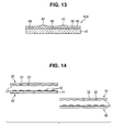
- An upper mold 20 as illustrated in Fig. 14 is a mold manufactured using the master model 40 regarding the shape of one surface of the wafer-level lens array 10. Also, a lower mold 30 is a mold manufactured using a master model 50 regarding the shape of the other surface of the wafer-level lens array 10.
- a transfer surface 21 of the upper mold 20 is formed by transfer of the shape of the master model 40 thereto, and ultimately, is formed in an inverse shape of one surface shape of the wafer-level lens array 10. Accordingly, on the transfer surface 21, lens forming surfaces 22 are two-dimensionally arranged to correspond to the arrangement of the lens portions 6 of the wafer-level lens array 10. Also, the lens forming surfaces 22 are molded as concave-shaped spherical surfaces to correspond to the lens surfaces 6a which are convex-shaped spherical surfaces.
- a transfer surface 31 of the lower mold 30 is formed by transfer of the shape of the master model 50 thereto, and ultimately, is formed in an inverse shape of the other surface shape of the wafer-level lens array 10.
- lens forming surfaces 32 are two-dimensionally arranged to correspond to the arrangement of the lens portions 6 of the wafer-level lens array 10. Also, the lens forming surfaces 32 are molded as concave-shaped spherical surfaces to correspond to the lens surfaces 6b which are convex-shaped spherical surfaces.
- the upper mold 20 and the lower mold 30 are manufactured by an elecroforming process.
- the manufacturing of the upper mold 20 by the elecroforming process is as follows. First, a conductive layer is formed on the surface of the master model 40. Then, the master model 40 on which the conductive layer is formed is soaked in a nickel plating solution, and an electric field is formed in the solution in a state where the conductive layer serves as a negative electrode. Accordingly, nickel Ni is extracted and accumulated on the surface of the master model 40. The deposits of the nickel Ni become the upper mold 20 and the contact surface with the master model 40 becomes the transfer surface 21.
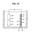
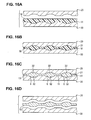
- a molding material M is supplied onto the transfer surface 31 of the lower mold 30, and the molding material M is made to be spread over the transfer surface 31.
- the molding material M is preheated to improve the liquidity, and then is supplied onto the transfer surface 31 (see Fig. 16A ).
- an energy-curable resin composition may be used as the molding material M.
- the energy-curable resin composition may be either a resin composition that is cured by heat or a resin composition that is cured by irradiation of active energy rays (for example, ultraviolet rays).
- the molding material has an appropriate liquidity before it is cured from the viewpoint of the moldability such as the transfer aptitude of the mold shape and so on. Specifically, it is preferable that the molding material is liquid at ambient temperature and its viscosity is about 1000 to 50000mPa.s.
- the molding material is heat-resistant to the extent that it is not thermally deformed through a reflow process.
- the glass transition temperature of the cured material is preferably equal to or greater than 200°C, more preferably equal to or greater than 250°C, and particularly preferably equal to or greater than 300°C.
- effective means may be (1) means for heightening the crosslink density per unit volume, (2) means using a resin having rigid ring structure (for example, an aliphatic ring structure such as cyclohexane, norbornane, tetracyclododecane, and the like, an aromatic ring structure such as benzene, naphthalene, and the like, a cardo structure such as 9,9'-biphenylfluorene and the like, resins having a spiro structure such as spirobiindan and the like, specific examples may include resins described in Japanese Unexamined Patent Application Publication Nos.
- a resin having rigid ring structure for example, an aliphatic ring structure such as cyclohexane, norbornane, tetracyclododecane, and the like, an aromatic ring structure such as benzene, naphthalene, and the like, a cardo structure such as 9,9'-biphenylfluor
- the material is a resin composition having a small volume contraction rate by curing reaction. It is preferable that the volume contraction rate of the resin composition is equal to or less than 10%, it is more preferable that the volume contraction rate is equal to or less than 5%, and it is furthermore preferable that the volume contraction rate is equal to or less than 3%.
- the resin composition having a low volume contraction rate may be (1) resin compositions including a high molecular weight curing agent (prepolymer or the like) (for example, those disclosed in Japanese Unexamined Patent Application Publication Nos. 2001-19740 , 2004-302293 , and 2007-211247 .
- the number-average molecular weight of the high molecular weight curing agent is preferably in the range of 200 to 100,000, more preferably in the range of 500 to 50,000, and particularly preferably in the range of 1,000 to 20,000. Also, the value calculated as the number-average molecular weight of the high molecular weight curing agent/the number of curing reactive groups is preferably in the range of 50 to 10,000, more preferably in the range of 100 to 5,000, and particularly preferably in the range of 200 to 3,000), (2) resin compositions including non-reactive material (organic/inorganic particles, non-reactive resins, and the like) (for example, those described in Japanese Unexamined Patent Application Publication Nos.
- resin compositions including a low-contraction crosslink reactive group (for example, a ring-opening polymerizable group (for example, an epoxy group (for example, those described in Japanese Unexamined Patent Application Publication No. 2004-210932 ), an oxetanyl group (for example, those described in Japanese Unexamined Patent Application Publication No. 8-134405 ), an episulphide group (for example, those described Japanese Unexamined Patent Application Publication No. 2002-105110 ), a ring type carbonate group (for example, those described in Japanese Unexamined Patent Application Publication No.
- a low-contraction crosslink reactive group for example, a ring-opening polymerizable group (for example, an epoxy group (for example, those described in Japanese Unexamined Patent Application Publication No. 2004-210932 ), an oxetanyl group (for example, those described in Japanese Unexamined Patent Application Publication No. 8-134405 ), an episulphide group (for example, those described Japanese Une
- resin compositions including an expansive material for example, those described in Japanese Unexamined Patent Application Publication Nos. 2004-2719 and 2008-28417 ), or the like.
- the above-described resin compositions may be appropriately used.
- a plurality of cure shrinkage reduction means in combination for example, a resin composition including prepolymer and particles containing ring-opening polymerizable group, and so on).
- the Abbe number (vd) is preferably equal to or larger than 50, more preferably equal to or larger than 55, and particularly preferably equal to or larger than 60.
- the refractive index (nd) is preferably equal to or larger than 1.52, more preferably equal to or larger than 1.55, and particularly preferably equal to or larger than 1.57.
- the above-described resin is a resin of an aliphatic group, and particularly, a resin having an aliphatic ring structure (for example, resins having a ring structure, such as such as cyclohexane, norbornane, adamantine, tricyclodecane, tetracyclododecane, and the like, and specifically, those disclosed in Japanese Unexamined Patent Application Publication Nos. 10-152551 , 2002-212500 , 2003-20344 , 2004-210932 , 2006-199790 , 2007-2144 , 2007-284650 , 2008-105999 , and the like).
- a resin having an aliphatic ring structure for example, resins having a ring structure, such as such as cyclohexane, norbornane, adamantine, tricyclodecane, tetracyclododecane, and the like, and specifically, those disclosed in Japanese Unexamined Patent Application Publication Nos. 10-152551
- the Abbe number (vd) is equal to or smaller than 30, it is more preferable that the Abbe number is equal to or smaller than 25, and it is furthermore preferable that the Abbe number is equal to or smaller than 20.
- the refractive index (nd) is preferably equal to or larger than 1.60, more preferably equal to or larger than 1.63, and particularly preferably equal to or larger than 1.65.
- the above-described resin is preferably a resin having an aromatic structure, for example, a resin including a structure, such as 9,9'-diarylfluorene, naphthalene, benzothiazole, benzotriazole, and the like (specific examples include those disclosed in Japanese Unexamined Patent Application Publication Nos. 60-38411 , 10-67977 , 2002-47335 , 2003-238884 , 2004-83855 , 2005-325331 ,and 2007-238883 , International Publication No. 2006/095610 , Patent No. 2537540 , and the like).
- a resin having an aromatic structure for example, a resin including a structure, such as 9,9'-diarylfluorene, naphthalene, benzothiazole, benzotriazole, and the like (specific examples include those disclosed in Japanese Unexamined Patent Application Publication Nos. 60-38411 , 10-67977 , 2002-47335 , 2003-238884
- inorganic particles examples include oxide particles, sulfide particles, selenide particles, and telluride particles.
- examples of inorganic particles may include zirconium oxide, titanium oxide, zinc oxide, tin oxide, niobium oxide, cerium oxide, aluminum oxide, lanthanum oxide, yttrium oxide, oil zinc, and the like.
- the particles such as titanium oxide, tin oxide, zirconium oxide, and the like.
- the inorganic particles may by used singly, or two or more kinds of inorganic particles may be used in combination. Also, a composite including a plurality of components may be used.
- the inorganic particles are used for diverse purposes such as reduction of photocatalytic activation, reduction of absorption rate, and the like, dissimilar metals may be doped, a surface layer may be coated with dissimilar metal oxide such as silica, alumina, and the like, or surface modification may be performed with dispersing agents having silane coupling agents, titanate coupling agents, organic acids (carboxylic acids, sulfonic acids, phosphoric acids, phosphonic acids, and the like), or organic acid group.
- the number-average particle size of the inorganic particles may be about 1nm to 1000nm. If the particle size is too small, the characteristics of the material may be changed, while if the particle size is too large, the effect of Rayleigh scattering becomes severe.
- the particle size is preferably 1 to 15nm, more preferably 2nm to 10nm, and particularly preferably 3nm to 7nm. Also, it is preferable that the distribution of the particle size of inorganic particles becomes narrower.
- the numerical regulation range as described in Japanese Unexamined Patent Application Publication No. 2006-160992 well suits the preferable particle diameter range.
- the number-average first-order particle size can be measured by an X-ray diffraction (XRD) device or a transmission electronic microscope (TEM).
- the refractive index of the inorganic particles is preferably 1.90 to 3.00 at 22°C in the wavelength of 589nm, more preferably 1.90 to 2.70, and particularly preferably 2.0 to 2.70.
- the content of the inorganic particles in the resin is preferably equal to or larger than 5 w%, more preferably 10 to 70 w%, and particularly preferably 30 to 60 w%.
- dispersing agents including a functional group having a reactivity with a resin monomer that forms a matrix (for example, those described in examples or the like in Japanese Unexamined Patent Application Publication No. 2007-238884 ), a block copolymer composed of a hydrophobic segment and a hydrophilic segment (for example, those described in Japanese Unexamined Patent Application Publication No. 2007-211164 ), or a resin having a functional group that can form an optional chemical bond with inorganic particles at a polymer end or side chain (for example, those described in Japanese Unexamined Patent Application Publication Nos. 2007-238929 and 2007-238930 ).
- dispersing agents including a functional group having a reactivity with a resin monomer that forms a matrix (for example, those described in examples or the like in Japanese Unexamined Patent Application Publication No. 2007-238884 ), a block copolymer composed of a hydrophobic segment and a hydrophilic segment (for example, those described in Japanese Unex
- additives such as a known release agents such as silicon series, fluorine series, long-chain alkyl group-containing compositions, and the like, or antioxidants such as hindered phenol and the like, may be appropriately added.
- a curing catalyst or initiator may be combined with the resin composition.
- a specific example includes a compound that accelerates the curing reaction (radical polymerization or ion polymerization) by heat or activation energy rays, as described in Japanese Unexamined Patent Application Publication No. 2005-92099 Paragraph Number [0063] to [0070].
- the addition amount of the curing reaction accelerating agents is not uniformly prescribed due to the kind of catalyst or initiator or a difference of the curing reaction regions, but in general, it is preferable that the addition amount is about 0.1 to 15 w% of the total amount of solids in the cure reactive resin composition, and it is more preferable that the addition amount is about 0.5 to 5 w%.
- the resin composition may be produced by properly combining the above-described components. In this case, if other components are soluble in the liquefied low-molecule monomer (reactive diluents) and so on, it is not required to add a separate solvent. If the resin composition does not suit this case, the curable resin composition can be produced by dissolving the components using the solvent.
- the solvent that can be used as the curable resin composition there is no special limit, and it is sufficient if the composition is not deposited and can be uniformly dissolved or dispersed.
- the solvent may be ketone (for example, acetone, methyl ethyl ketone, methyl isobutyl ketone, and the like), esters (for example, ethyl acetate, butyl acetate, and the like), ethers (for example, tetrahydrofuran, 1,4-dioxane, and the like), alcohol (for example, methanol, ethanol, isopropyl alcohol, buthanol, ethylene glycol, and the like), aromatic hydrocarbons (for example, toluene, xylene, and the like), water, and the like.
- the curable composition includes a solvent, it is preferable to perform the mold shape transfer operation after drying the solvent by casting the composition on the substrate or mold.
- the upper mold 20 is lowered, the molding material M is inserted between the transfer surface 21 of the upper mold 20 and the transfer surface 31 of the lower mold 30, and then the upper and lower molds 20 and 30 are compressed to transform the molding material M so that the molding material M is molded on both the transfer surfaces 21 and 31 (see Fig. 16B ).
- the molding material M which is positioned between the transfer surface 21 of the upper mold 20 and the transfer surface 31 of the lower mold 30, is cured by giving curing energy to the molding material M through heating or irradiation of active energy rays, resulting in that the wafer-level lens array 10 is obtained.
- Lens portions 6 are formed between the lens forming surfaces 22 of the upper mold 20 and the lens forming surfaces 32 of the lower mold 30, which form a pair.
- the substrate portion 11 is formed between the transfer surfaces 21 of the upper mold 20 and the transfer surfaces 31 of the lower mold 30 except for the lens forming surfaces 22 and 32 (see Fig. 16C ).
- the wafer-level lens array 10 is separated from the upper mold 20 and the lower mold 30 (see Fig. 16D ).
- the master model 40 that is used in the manufacturing method is configured by arranging a plurality of members 42 corresponding to lenses on which curved surfaces that correspond to either of the lens surfaces 6a and 6b of one surface and the other surface of the lens portions 6 of the wafer-level lens array 10 are installed.
- a master model that is configured by arranging a plurality of members corresponding to lenses, on which both the curved surfaces corresponding to the lens surfaces 6a of the lens portions 6 and the curved surfaces corresponding to the lens surfaces 6b are installed will be described.
- the lens surfaces 6a and 6b on one surface and the other surface of the lens portions 6 are convex-shaped spherical surfaces, concave-shaped spherical surfaces, or non-spherical surfaces, and have power in all.
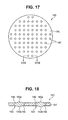
- a master model 140 as illustrated in Figs. 17 and 18 includes a substrate 141 and a plurality of members 142 corresponding to lenses.
- the members 142 corresponding to lenses have curved surfaces 143a and 143b formed on one surface and the other surface thereof, and a flange portions 144 including circumferences of portions inserted between the curved surfaces 143a and 143b, respectively.
- the curved surfaces 143a on one surface side are formed in the same shape of that of the lens surfaces 6a on one surface side of the lens portions 6 of the wafer-level lens array 10, and the curved surfaces 143b on the other surface side are formed in the same shape of that of the lens surfaces 6b on the other surface side of the lens portions 6 of the wafer-level lens array 10.
- the thickness of the portions inserted between the curved surfaces 143a and 143b is the same as the thickness of the lens portions 6 of the wafer-level lens array 10, and the thickness of the flange portions 144 is the same as the thickness of the substrate portion 11 of the wafer-level lens array 10.
- the curved surfaces 143a and 143b are formed so that their center axes coincide with each other.
- the coaxiality that is permitted with respect to the center axes of the curved surfaces 143a and 143b is based on the coaxiality that is permitted with respect to the optical axes of the lens surfaces 6a and 6b on one surface and the other surface of the lens portions 6 of the lens module 3 in the imaging unit 1 (see Fig. 1 ), and for example, is typically 1 to 2 ⁇ m in the imaging unit mounted on a portable phone or the like.
- the members 142 corresponding to lenses that satisfy the above-described coaxiality may be formed, for example, by glass press molding or resin injection molding.
- the substrate 141 is in the form of a wafer having the same size as that of the wafer-level lens array 10, and its thickness is the same as that of the substrate portion 11 of the wafer-level lens array 10.
- a plurality of through-holes 145 which penetrate the substrate 141 in the thickness direction d of the substrate 141 and have a size enough to accommodate the members 142 inserted into the through-holes, respectively, is formed.
- the through-holes 145 are arranged on the substrate 141 in the same lines as those of the lens portions 6 in the wafer-level lens array 10.
- the material of the substrate 141 is not specifically restricted, and for example, glass or resin is used as the material of the substrate 141.
- adhesives 150 are spread.
- the adhesives for example, a photocurable resin material or a thermosetting resin material is used.
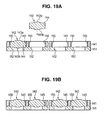
- a fixture 151 is attached on the other surface of the substrate 141.
- a plurality of through-holes 152 which communicate with the through-holes 145 of the substrate 141, respectively, is formed.
- the through-hole 152 has a diameter that is larger than that of the curved surface 143b of one side of the members 142 corresponding to lenses, and is smaller than that of the flange portion 144.
- the members 142 corresponding to lenses are inserted into the through-holes 145 of the substrate 141, respectively.
- the fixture 151 exposes the curved surfaces 143b of the other surface of the member 142 inserted into the through-holes 145 of the substrate 141 through the through-holes 152, and supports the flange portions 144 of the members 142 corresponding to lenses on the circumferences of the through-holes 152 to make all the members 142 corresponding to lenses have the same height (see Fig. 19A ).
- the members 142 corresponding to lenses are inserted into all the through-holes 145 of the substrate 141. Thereafter, in the case of using the UV-curable resin as the adhesives 150, the UV-curable resin is irradiated with UV rays, while in the case of using the thermosetting resin as the adhesives 150, the thermosetting resin is heated to cure the adhesives 150, and thus the respective members 142 corresponding to lenses are fixed to the substrate 141. After the members 142 corresponding to lenses are fixed to the substrate 141 by adhering, the fixtures 151 are separated from the substrate 141 (see Fig. 19B ).
- the plurality of members 142 corresponding to lenses is arranged in the same lines as those of the plurality of lens portions 6 in the wafer-level lens array 10, and is connected together in a body by the substrate 141. Accordingly, the obtained master model 140 has the same shape as the wafer-level lens array 10.
- a plurality of members 142 corresponding to lenses which are formed on one surface and the other surface of the curved surfaces 143a and 143b that have the same shape as the lens surfaces 6a and 6b formed on one surface and the other surface of the lens units 6 of the wafer-level lens array 10, is arranged, and their curved surfaces 143a and 143b are arranged on one surface and the other surface of the master model 140. It is relatively facilitated to form the curved surfaces 143a and 143b on one surface and the other surface of the members 142 corresponding to lenses with their center axes coinciding with each other at high precision. Accordingly, the center axes of the curved surfaces 143a and 143b, which form a pair, coincide with each other easily and at high precision over the whole master model 140.
- the mold as illustrated in Fig. 20 includes an upper mold 120 and a lower mold 130.
- the upper mold 120 has a transfer surface 121.
- the transfer surface 121 is formed through the transfer of the shape of one surface of the master model 140 to the transfer surface 121, and consequently, has an inverse shape of the shape of one surface of the wafer-level lens array 10.
- On the transfer surface 121 a plurality of lens forming surfaces 122 is formed in a matrix shape in the same lines as those of the curved surfaces 143a arranged on the surface side of the master model 140.
- the lens forming surfaces 122 are formed on the concave-shaped spherical surfaces corresponding to the curved surfaces 143a which are the convex-shaped spherical surfaces.
- the lower mold 130 has a transfer surface 131.
- the transfer surface 131 is formed through the transfer of the shape of the other surface of the master model 140 to the transfer surface 131, and consequently, has an inverse shape of the shape of the other surface of the wafer-level lens array 10.
- On the transfer surface 131 a plurality of lens forming surfaces 132 is formed in a matrix shape in the same lines as those of the curved surfaces 143b arranged on the other surface side of the master model 140.
- the lens forming surfaces 132 are formed on the concave-shaped spherical surfaces corresponding to the curved surfaces 143b which are the convex-shaped spherical surfaces.
- the upper mold 120 and the lower mold 130 are position determination portions that perform mutual position determination, and pin accommodation holes 123 and 133, which form pairs, are provided in a plurality of places of the upper mold 120 and the lower mold 130.
- the upper mold 120 and the lower mold 130 can be manufactured by an elecroforming method using the master model 140.
- pins 146 are installed to stand in a plurality of places of the master model 140.
- the pins 146 are arranged to penetrate the master model 140 in the thickness direction of the master model 140 so that they project to one surface side and the other surface side of the master model 140.
- Conductive layers are formed on one surface and the other surface of the master model 140.
- the master model 140 is soaked in a nickel plating solution, and an electric field is formed in the solution in a state where the conductive layer serves as a negative electrode. Accordingly, nickel Ni is extracted and accumulated on one surface and the other surface of the master model 140. The deposits on one surface of the master model 140 become the upper mold 120 and the deposits on the other surface of the master model 140 become the lower mold 130.
- the contact surface with the master model 140 becomes the transfer surface 121, and on the transfer surface 121, the lens forming surfaces 122 of an inverse shape of the curved surfaces 143a are arranged in the same lines as those of the curved surfaces 143a arranged on one surface side of the master model 140. Also, on the transfer surface 121, the pin accommodation holes 123, which are formed through the transfer of the shape of end portions of the pins 146 arranged to project to one surface side of the master model 140, are formed.
- the contact surface with the master model 140 becomes the transfer surface 131, and on the transfer surface 131, the lens forming surfaces 132 of an inverse shape of the curved surfaces 143b are arranged in the same lines as those of the curved surfaces 143b arranged on the other surface side of the master model 140. Also, on the transfer surface 131, the pin accommodation holes 133, which are formed through the transfer of the shape of end portions of the pins 146 arranged to project to the other surface side of the master model 140, are formed.
- the manufacturing of the upper mold 120 and the lower frame mole 130 is not limited to the electro-plating method.
- the molds may be manufactured by using glass or resin as the mold material and transferring shapes of one surface or the other surface of the master model 140 to the softened mold material.
- the molding material M is supplied onto the transfer surface 131 of the lower mold 130 (see Fig. 22A ).
- the upper mold 120 is lowered, the molding material M is inserted between the transfer surface 121 of the upper mold 120 and the transfer surface 131 of the lower mold 130, and then the upper and lower molds 120 and 130 are compressed to transform the molding material M so that the molding material M is modeled on both the transfer surfaces 121 and 131.
- the mutual position determination of the upper frame 120 and the lower frame 130 is performed. Accordingly, the center axes of the lens forming surfaces 122 of the upper mold 120 and the lens forming surfaces 132 of the lower mold 130 coincide with each other at high precision (see Fig. 22B ).
- the molding material M which is positioned between the transfer surface 121 of the upper frame 120 and the transfer surface 131 of the lower mold 130, is cured by giving curing energy to the molding material M through heating or irradiation of active energy rays, resulting in that the wafer-level lens array 10 is obtained.
- Lens portions 6 are formed between the lens forming surfaces 122 of the upper mold 120 and the lens forming surfaces 132 of the lower mold 130, which form a pair.
- the substrate portion 11 is formed between the transfer surfaces 121 of the upper mold 120 and the transfer surfaces 131 of the lower mold 130 except for the lens forming surfaces 122 and 132 (see Fig. 22C ).
- the wafer-level lens array 10 is separated from the upper mold 120 and the lower mold 130 (see Fig. 22D ).
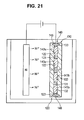
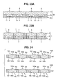
- a wafer-level lens array 10 is laminated on a sensor array 60 through the intervention of a spacer member 70 to form a body, and then the wafer-level lens array 10, the sensor array 60, and the spacer member 70 are cut together to obtain a plurality of imaging units 1 (see Fig. 1 ).
- the sensor array 60 includes a wafer 61 formed of a semiconductor material such as silicon.
- the wafer 61 is formed with the same size as that of the wafer-level lens array 10.
- On the wafer 61 a plurality of solid-state imaging devices 4 is formed.
- the solid-state imaging devices 4 are arranged in a matrix shaped in the same lines as those of the plurality of lens portions 6 of the wafer-level lens array 10 on the wafer 61.
- the spacer member 70 is a member that is in a wafer shape with the same size as that of the wafer-level lens array 10. On the spacer member 70, a plurality of through-holes 71 is formed. The through-holes 71 formed on the spacer member 70 are arranged in a matrix shape in the same lines as those of the plurality of lens portions 6 of the wafer-level lens array 10.
- the spacer member 70 is placed on the surface of the sensor array 60, on which the plurality of sold-state imaging devices 4 is arranged, and both the spacer member 70 and the sensor array 60 are bonded together. Then, the wafer-level lens array 10 is placed on the spacer member 70, and the wafer-level lens array 10 and the spacer member 70 are bonded together. By the spacer member 70, there is a predetermined distance between the respective lens portions 6 of the wafer-level lens array 10 and the corresponding solid-state imaging devices 4 of the sensor array 60 (see Fig. 23A ).
- a laminated body 80 in which the wafer-level lens array 10, the sensor array 60, and the spacer member 70 are united, is cut in a lattice shape.
- the wafer-level lens array 10 is divided into a plurality of lens modules 3 including the lens portions 6, respectively, and the sensor array 60 is divided into a plurality of sensor modules 2 including the imaging devices, respectively.
- the spacer member 70 is divided into a plurality of spacers 9 which are interposed between the lens modules 3 and the corresponding sensor modules 2, respectively, to connect the lens modules 3 and the sensor modules 2, respectively.
- One set of a lens module 3, a sensor module 2, and a spacer 9, which are bonded in a body, constitutes one imaging unit 1 (see Fig. 23B ).
- one wafer-level lens array 10 is laminated on the sensor array 60.
- a plurality of wafer-level lens arrays 10 may be laminated.
- the respective wafer-level lens array 10 are sequentially laminated in a state where the spacer member 70 is interposed between the sensor array 60 and the wafer-level lens array 10, and another spacer member that is equal to the spacer member 70 is interposed between the wafer-level lens arrays 10 which are laminated on the sensor array 60.
- the shape of the lens portions 6 may differ for each wafer-level lens array 10.
- the coaxiality that is permitted with respect to the optical axes of the lens portions 6 of the wafer-level lens array 10 and the optical axes of the lens portions 6 of the other corresponding wafer-level lens array 10 depends upon the pitch accuracy of the arrangement of the lens portions 6 in the respective wafer-level lens arrays 10 and also depends upon the pitch accuracy of the arrangement of the members 142 corresponding to lenses in their master model 140.
- the master models 140A and 140B which are master models of the laminated lens arrays, have the same construction as that of the above-described master model 140, and each of the master models includes a substrate 141 on which a plurality of through-holes 145 is arranged, and a plurality of members 142 corresponding to lenses inserted into the through-holes 145, respectively.
- the shapes (diameters) of the curved surfaces 143a and 143b formed on one surface and the other surface thereof may differ.
- the wafer-level lens array 10 copied using the mold to which the shape of the master model 140A has been transferred and the wafer-level lens array 10 copied using the mold to which the shape of the master model 140B has been transferred have different shapes (diameters) of the lens portions 6.
- the substrate 141 included in the master model 140A and the substrate 141 included in the master model 140B are manufactured by laminating their substrate materials 141' and forming through-holes 145 on the two laminated substrate materials 141' through a collective boring process using a drill or end mill.
- the pitches of the arrangements of the through-holes 145 in their substrates 141 are equal to each other in the master model 140A and the master model 14B, and thus the pitches of the arrangements of the members 142 corresponding to lenses inserted into the through-holes 145, respectively, are equal to each other in the master model 140A and the master model 140B. Accordingly, the pitches of the arrangements of the lens portions 6 in the wafer-level lens array 10 copied using the mold to which the shape of the master model 140A has been transferred and the pitches of the arrangements of the lens portions in the wafer-level lens array 10 copied using the mold to which the shape of the master model 140B has been transferred become equal to each other in the same manner.
- the diameters of the curved surfaces 143a and 143b formed on one surface and the other surface thereof are different from each other.
- the diameter of the through-holes 145 collectively formed on the substrate 141 included in the master model 140A and the substrate 141 included in the master model 140B is set to be larger than the diameter which is larger one between the diameter of the curved surfaces 143a and 143b of the members 142 corresponding to lenses included in the master model 140A and the diameter of the curved surfaces 143a and 143b of the members 142 corresponding to lenses included in the master model 140B.
- the flange portions 144 are filled between the portions inserted in the curved surfaces 143a and 143b and inner peripheries of the through-holes 145, respectively.
- a master model 140a as illustrated in Fig. 26 is a master model in the case where a spacer portion that corresponds to the spacer member 70 in the laminated body 80 is formed in a body with the wafer-level lens array 10.
- This master model 140 includes a substrate 141 and a plurality of members 142 corresponding to lenses.
- the substrate 141 is in a wafer shape with the same size as that of the wafer-level lens array 10, and its thickness is the sum of thickness of the substrate portion 11 of the wafer-level lens array 10 and the thickness of the spacer member 70.
- the other surface side of the substrate 141 projects over the curved surfaces 143b of the other surface side of the members 142 corresponding to lenses to form the spacer portion 147. That is, the spacer portion 147 is formed by the thickness of the substrate 141.
- a spacer portion that corresponds to the spacer portion 147 of the master model 140 is formed in a body.
- the spacer portion is interposed between the sensor array 60 and another wafer-level lens array 10 so as to provide a predetermined distance between the respective lens portions 6 and the corresponding devices (the solid-state imaging devices 4 of the sensor array 60 or the lens portions 6 of another wafer-level lens array 10).
- the master model 140b as illustrated in Figs. 27 and 28 includes a plurality of members 142 corresponding to lenses arranged in the same lines as those of the plurality of lens portions 6 of the wafer-level lens array 10.
- the curved surfaces 143a and 143b are formed on one surface and the other surface of the members 142 corresponding to lenses, and the members 142 corresponding to lenses have flange portions 144 that surround the circumference of the portions inserted in the curved surfaces 143a and 143b.
- the flange portions 144 are formed to be filled between the neighboring members 142 corresponding to lenses, and in the illustrated example, they are in the shape of tetragons as seen in the plan view.
- the members 142 corresponding to lenses are bonded with the flange portions 144 of the members 142 corresponding to lenses neighboring the flange portions 144 thereof.
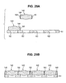
- a plurality of members 142 corresponding to lenses is preproduced, and adhesives 150 such as photocurable resin thermosetting resin are spread on side surfaces of the flange portions 144. Then, one member 142 corresponding to a lens is arranged on the fixture 151, and based on this, other members 142 corresponding to lenses are arranged to neighbor the member 142 corresponding to a lens already arranged on the fixture 151. In this case, by contacting the side surfaces of the flange portions 144, the positions of the members 142 corresponding to lenses placed on the fixture 151 are determined (see Fig. 29A ).
- the members 142 corresponding to lenses are arranged in the same lines as those of the lens portions 6 on the fixture 151.
- the members 42 corresponding to lenses are irradiated with UV rays
- thermosetting resin is used as the adhesives 150
- the adhesives 150 are heated and then is cured to combine and connect the neighboring members 142 corresponding to lenses to their flange portions 144.
- putties 148 are filled up on the fixture 151 to surround the circumference of the plurality of members 142 corresponding to lenses in a body, so that the whole wafer is formed (see Fig. 29B ).
- the master model 140c as illustrated in Fig. 30 includes spacer portions 147 formed on one surface and the other surface thereof.
- frame portions 147a and 147b are installed along the edges of one surface and the other surface thereof.
- the frame portions 147a surrounds the curved surfaces 143a on the surface side of the members 142 corresponding to lenses, and projects over the curved surfaces 143a.
- the frame portions 147b surrounds the curved surfaces 143b on the other surface side of the members 142 corresponding to lenses, and projects over the curved surfaces 143b.
- the frame portions 147a and 147b on one surface and the other surface of the members 142 corresponding to lenses are bonded to the frame portions 147a and 147b on one surface and the other surface of the neighboring members 142 corresponding to lenses, respectively.
- the frame portions 147a on the surface side of the members 142 corresponding to lenses are integrated to form a spacer portion 147 on the surface side of the master model 140c, and the frame portions 147b on the other surface side of the members 142 corresponding to lenses are integrated to form a spacer portion 147 on the other surface side of the master model 140c.
- spacer portions that correspond to the spacer portions 147 of one surface and the other surface of the master model 140c are formed in a body.
- the spacer member 70 there is a predetermined distance between the respective lens portions 6 and the corresponding devices (solid-state imaging devices 4 of the sensor array 60 or the lens portions 6 of another wafer-level lens array 10).
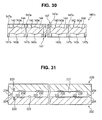
- the mold as illustrated in Fig. 31 includes an upper mold 220 and a lower mold 230.
- the upper mold 220 has a transfer surface 221.
- the transfer surface 221 is formed by transferring the surface shape of the master model 140 thereto, and a plurality of lens forming surfaces 222 is formed in a matrix shape in the same lines as those of the curved surfaces 143a arranged on the surface side of the master model 140.
- the lower mold 230 has a transfer surface 231.
- the transfer surface 231 is formed by transferring the other surface shape of the master model 140 thereto, and a plurality of lens forming surfaces 232 is formed in a matrix shape in the same lines as those of the curved surfaces 143b arranged on the other surface side of the master model 140.
- tapered surfaces 224 and 234 that match each other are installed along their outer peripheries. Also, in order to restrict the relative rotation about the center axes thereof, pairs of pin accommodation holes 223 and 233 are formed in positions apart from the center axes on the upper mold 220 and the lower mold 230.
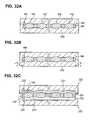
- a pin 146 is vertically installed in a position that is apart from the center axes of the master model 140, and a conductive layer is formed on the whole surface of the master model 140 including the pin 146. Then, nickel (Ni) is extracted and accumulated on the whole surface of the master model 140 by an electro-plating method. Accordingly, Ni accumulation 250 is accumulated on the master model 140 (see Fig. 32A ).
- the accumulation 250 is divided into two in its thickness direction by incising the circumference of the accumulation 250 from the circumference of the accumulation at a depth reaching the outer periphery of the master model 140 and at a predetermined angle ⁇ ( ⁇ 90°) about the outer periphery of the master model 140 (in other words, about the center axis of the master model 140) (see Fig. 32B ).
- One of the divided accumulations 250 includes the transfer surface 221 that is formed by transferring the surface shape of the master model 140 thereto, and this becomes the upper mold 220. Also, the other of the divided accumulations 250 includes the transfer surface 231 that is formed by transferring the other surface shape of the master model 140 thereto, and this becomes the lower mold 230. Also, the cut surface remaining on the upper mold 220 forms a tapered surface 224, and the cut surface remaining on the lower mold 230 forms a tapered surface 234 (see Fig. 32C ).
- a master model that is an original of a mold for molding a lens array on which a plurality of lens portions is arranged
- a plurality of members corresponding to lenses having curved surfaces molded in the same shape as that of lens surfaces of the lens portions is arranged in the same order as those of the plurality of lens portions in the lens array and is connected in a body.
- the lens portions of the lens array have lens surfaces having power on one surface and the other surface thereof, and the respective members corresponding to lenses have curved surfaces molded in the same shape as that of lens surfaces on one surface and the other surface thereof.
- a method of manufacturing a master model that is an original of a mold for molding a lens array on which a plurality of lens portions is arranged includes the steps of forming a plurality of members corresponding to lenses having curved surfaces molded in the same shape as lens surfaces of the lens portions, arranging one or more of the plurality of members corresponding to the lenses in the same order as the plurality of lens portions in the lens array, and integrally connecting the plurality of arranged members corresponding to the lenses.
- the lens portions of the lens array have lens surfaces having power on one surface and the other surface thereof, and the respective members corresponding to lenses have curved surfaces molded in the same shape as that of lens surfaces on one surface and the other surface thereof.
- the plurality of members corresponding to lenses includes flange portions that are filled between the neighboring members corresponding to lenses when the members are arranged, and the plurality of members corresponding to lenses is arranged so that their flange portions contact each other.
- the plurality of members corresponding to lenses is arranged on the substrate.
- the neighboring members corresponding to lenses are pre-connected when the members are arranged.
- a mold of a lens array in which a plurality of lens portions are arranged is disclosed, which is formed by transferring the shape of the master model to a mold material.
- a mold of a lens array in which a plurality of lens portions are arranged, which includes an upper mold formed by transferring one surface shape of the master model to a first mold material, and a lower mold formed by transferring the other surface shape of the master model to a second mold material, wherein a position determination portion for performing a mutual position determination is installed on the upper mold and the lower mold.
- a method of manufacturing a mold of a lens array in which a plurality of lens portions are arranged, which includes the steps of installing a plurality of convex on one surface of a master model and installing convex portions in positions of the other surface of the master model, which correspond to the plurality of convex portions of the surface, and forming an upper mold by transferring one surface shape of the master model to a mold material and forming a lower mold by transferring the other surface shape of the master model to a mold material.
- a method of manufacturing a mold of a lens array in which a plurality of lens portions are arranged, which includes the steps of surrounding a master model with a mold material and transferring one surface shape and the other surface shape of the master model to the mold material, and dividing the mold material into an upper mold to which one surface shape of the master model is transferred and a lower mold to which the other surface shape of the master model is transferred by cutting the mold material.
- a lens array made by forming a lens material using the mold for the lens array is disclosed.
- a lens module that is separated from the lens array to include one lens portion is disclosed.
- an imaging unit including a sensor module including solid-state imaging devices and at least one lens module that forms an image on the solid-state imaging devices, wherein the lens module is the above-described lens module.
Landscapes
- Engineering & Computer Science (AREA)
- Manufacturing & Machinery (AREA)
- Mechanical Engineering (AREA)
- Health & Medical Sciences (AREA)
- Ophthalmology & Optometry (AREA)
- Solid State Image Pick-Up Elements (AREA)
- Moulds For Moulding Plastics Or The Like (AREA)
- Lens Barrels (AREA)
- Studio Devices (AREA)
Applications Claiming Priority (3)
| Application Number | Priority Date | Filing Date | Title |
|---|---|---|---|
| JP2009215958 | 2009-09-17 | ||
| JP2009215961 | 2009-09-17 | ||
| JP2010118286A JP2011084060A (ja) | 2009-09-17 | 2010-05-24 | レンズアレイのマスターモデル及びその製造方法 |
Publications (2)
| Publication Number | Publication Date |
|---|---|
| EP2298543A2 true EP2298543A2 (de) | 2011-03-23 |
| EP2298543A3 EP2298543A3 (de) | 2016-09-07 |
Family
ID=43280244
Family Applications (1)
| Application Number | Title | Priority Date | Filing Date |
|---|---|---|---|
| EP10176858.8A Withdrawn EP2298543A3 (de) | 2009-09-17 | 2010-09-15 | Mastermodell für eine Linsenanordnung und Herstellungsverfahren dafür |
Country Status (4)
| Country | Link |
|---|---|
| US (1) | US8416498B2 (de) |
| EP (1) | EP2298543A3 (de) |
| JP (1) | JP2011084060A (de) |
| CN (1) | CN102019662B (de) |
Families Citing this family (28)
| Publication number | Priority date | Publication date | Assignee | Title |
|---|---|---|---|---|
| WO2010114483A1 (en) * | 2009-04-03 | 2010-10-07 | Ether Precision, Inc. | Methods and devices for manufacturing an array of lenses |
| JP2012194455A (ja) * | 2011-03-17 | 2012-10-11 | Enplas Corp | レンズアレイ |
| JP5840861B2 (ja) * | 2011-05-09 | 2016-01-06 | 東芝機械株式会社 | 成形体の設置方法および成形体の設置装置 |
| JP5568599B2 (ja) * | 2011-06-30 | 2014-08-06 | エルジー イノテック カンパニー リミテッド | レンズユニット、その製造方法、及びこれを含むカメラモジュール |
| US9642606B2 (en) | 2012-06-27 | 2017-05-09 | Camplex, Inc. | Surgical visualization system |
| US8882662B2 (en) | 2012-06-27 | 2014-11-11 | Camplex, Inc. | Interface for viewing video from cameras on a surgical visualization system |
| CN110061018B (zh) * | 2013-05-21 | 2023-11-28 | 弗托斯传感与算法公司 | 全光透镜在光传感器衬底上的单片集成 |
| EP2999414B1 (de) | 2013-05-21 | 2018-08-08 | Camplex, Inc. | Chirurgische visualisierungssysteme |
| EP3046458B1 (de) | 2013-09-20 | 2020-10-21 | Camplex, Inc. | Chirurgische visualisierungssysteme |
| WO2015042460A1 (en) | 2013-09-20 | 2015-03-26 | Camplex, Inc. | Surgical visualization systems and displays |
| US20150115129A1 (en) * | 2013-10-29 | 2015-04-30 | Omnivision Technologies, Inc. | Coated Diamond-Turned Replication Master And Associated Process |
| US10702353B2 (en) | 2014-12-05 | 2020-07-07 | Camplex, Inc. | Surgical visualizations systems and displays |
| US9377603B1 (en) * | 2015-01-26 | 2016-06-28 | Omnivision Technologies, Inc. | Low-profile hybrid lens systems and methods for manufacturing the same |
| JP6490443B2 (ja) | 2015-02-20 | 2019-03-27 | 株式会社エンプラス | 複合体およびその製造方法 |
| WO2016154589A1 (en) | 2015-03-25 | 2016-09-29 | Camplex, Inc. | Surgical visualization systems and displays |
| CN104960130B (zh) * | 2015-07-23 | 2017-03-22 | 长沙理工大学 | 一种小口径非球面玻璃透镜的精密热压成型模具 |
| WO2017080842A1 (en) * | 2015-11-09 | 2017-05-18 | Philips Lighting Holding B.V. | Method for producing an optical component by 3d printing, an optical component and a lighting device |
| WO2017091704A1 (en) | 2015-11-25 | 2017-06-01 | Camplex, Inc. | Surgical visualization systems and displays |
| JP2019529972A (ja) | 2016-08-26 | 2019-10-17 | モレキュラー インプリンツ, インコーポレイテッドMolecular Imprints,Inc. | モノリシック高屈折率フォトニックデバイス |
| US10056428B2 (en) * | 2016-09-07 | 2018-08-21 | Semiconductor Components Industries, Llc | Semiconductor device and method of forming curved image sensor region robust against buckling |
| WO2018086980A1 (en) * | 2016-11-14 | 2018-05-17 | Philips Lighting Holding B.V. | Led beam shaping |
| US10918455B2 (en) | 2017-05-08 | 2021-02-16 | Camplex, Inc. | Variable light source |
| EP3703610B1 (de) | 2017-11-02 | 2022-08-10 | Magic Leap, Inc. | Vorrichtung und verfahren zum mischen polymerer komponenten |
| US10880991B2 (en) * | 2018-04-04 | 2020-12-29 | Marvell Asia Pte, Ltd. | Apparatus and methods for enhancing signaling bandwidth in an integrated circuit package |
| CN111908774B (zh) * | 2019-05-10 | 2022-07-22 | 赵崇礼 | 透镜阵列的模具设备 |
| JP2021150556A (ja) * | 2020-03-23 | 2021-09-27 | ソニーセミコンダクタソリューションズ株式会社 | 撮像装置およびその製造方法 |
| CN111653580B (zh) * | 2020-06-08 | 2023-06-27 | 华天慧创科技(西安)有限公司 | 一种在感光芯片阵列上制作的透镜模组及方法 |
| JP7559653B2 (ja) * | 2021-03-31 | 2024-10-02 | Agc株式会社 | ガラス板の製造方法、及び転写型 |
Citations (44)
| Publication number | Priority date | Publication date | Assignee | Title |
|---|---|---|---|---|
| JPS6038411A (ja) | 1983-07-11 | 1985-02-28 | アイオーラブ・コーポレーシヨン | 2′―ヒドロキシ―5′―(ヒドロキシアルキル)フェニル―2h―ベンゾトリアゾール類 |
| JPH05209027A (ja) | 1991-09-24 | 1993-08-20 | Mitsubishi Rayon Co Ltd | 透明性に優れた複合体組成物およびその製法 |
| JPH06298883A (ja) | 1993-04-14 | 1994-10-25 | Dainippon Ink & Chem Inc | 成形材料及び人工大理石の製造方法 |
| JPH0762065A (ja) | 1993-08-20 | 1995-03-07 | Dainippon Ink & Chem Inc | 新規ポリカーボネート樹脂の製法および新規ポリカーボネート樹脂 |
| JPH08134405A (ja) | 1994-11-11 | 1996-05-28 | Toagosei Co Ltd | 缶外面用塗料組成物 |
| JP2537540B2 (ja) | 1988-07-19 | 1996-09-25 | 株式会社トクヤマ | 単量体組成物 |
| JPH09137043A (ja) | 1995-11-17 | 1997-05-27 | Mitsubishi Rayon Co Ltd | エポキシ樹脂組成物 |
| JPH1067977A (ja) | 1996-08-28 | 1998-03-10 | Nippon Steel Chem Co Ltd | 光ディスク用接着剤及び光ディスク |
| JPH1067970A (ja) | 1996-08-28 | 1998-03-10 | Nippon Steel Chem Co Ltd | 光ディスク用接着剤及び光ディスク |
| JPH10152551A (ja) | 1996-11-26 | 1998-06-09 | Sumitomo Bakelite Co Ltd | ノルボルナン環状カーボナート組成物 |
| JPH10298265A (ja) | 1997-05-01 | 1998-11-10 | Mitsubishi Rayon Co Ltd | 硬化性複合体組成物の製造方法 |
| JP2001019740A (ja) | 1999-07-09 | 2001-01-23 | Nippon Kayaku Co Ltd | 高エネルギー線感光性カチオン硬化型封止剤及び集積回路の接続封止方法 |
| JP2001247793A (ja) | 2000-03-02 | 2001-09-11 | Mitsubishi Rayon Co Ltd | フィルムコーティング用光硬化性組成物 |
| JP2002047335A (ja) | 2000-08-03 | 2002-02-12 | Osaka Gas Co Ltd | フルオレン系光重合性樹脂組成物、その硬化物および製造方法 |
| JP2002105110A (ja) | 2000-10-04 | 2002-04-10 | Mitsubishi Chemicals Corp | 硬化性組成物、その硬化物および用途 |
| JP2002212500A (ja) | 2001-01-23 | 2002-07-31 | Dainippon Ink & Chem Inc | 活性エネルギー線硬化型塗料用組成物 |
| JP2003020344A (ja) | 2001-07-10 | 2003-01-24 | Kureha Chem Ind Co Ltd | ポリグリコール酸成形物 |
| JP2003020334A (ja) | 2001-07-09 | 2003-01-24 | Toagosei Co Ltd | 光学部品用樹脂組成物及びそれを用いた光学部品 |
| JP2003055316A (ja) | 2001-08-06 | 2003-02-26 | Toagosei Co Ltd | ノルボルネン構造を有する基を有する化合物及びその製造方法 |
| JP2003238884A (ja) | 2002-02-15 | 2003-08-27 | Mitsubishi Alum Co Ltd | フィン用塗料組成物、フィン及びその製造方法並びに熱交換器 |
| JP2004002719A (ja) | 2002-03-25 | 2004-01-08 | Mitsubishi Rayon Co Ltd | (メタ)アクリル系樹脂組成物、(メタ)アクリル系樹脂成型品及びその製造方法 |
| JP2004083855A (ja) | 2002-06-28 | 2004-03-18 | Osaka Gas Co Ltd | フルオレン含有樹脂 |
| JP2004210932A (ja) | 2002-12-27 | 2004-07-29 | Daicel Chem Ind Ltd | 硬化性樹脂組成物及び硬化物 |
| JP2004302293A (ja) | 2003-03-31 | 2004-10-28 | Hitachi Chem Co Ltd | 感光性アルカリ可溶型組成物 |
| JP2005015666A (ja) | 2003-06-27 | 2005-01-20 | Shin Etsu Chem Co Ltd | 硬化性シリコーン樹脂組成物 |
| JP2005092099A (ja) | 2003-09-19 | 2005-04-07 | Fuji Photo Film Co Ltd | 硬化性樹脂組成物、及び光学物品、並びにそれを用いた画像表示装置 |
| JP2005325331A (ja) | 2004-04-14 | 2005-11-24 | Osaka Gas Co Ltd | 新規なフルオレン含有樹脂 |
| JP2006095610A (ja) | 2004-09-28 | 2006-04-13 | Hitachi Metals Ltd | 高温強度特性に優れた鋸刃 |
| JP2006131868A (ja) | 2004-10-08 | 2006-05-25 | Hitachi Chem Co Ltd | 樹脂組成物、及びそれを用いた光学部材とその製造方法 |
| JP2006160992A (ja) | 2004-12-10 | 2006-06-22 | Konica Minolta Opto Inc | 熱可塑性樹脂組成物及び光学素子 |
| JP2006199790A (ja) | 2005-01-19 | 2006-08-03 | Daicel Chem Ind Ltd | 硬化性樹脂組成物および層間絶縁膜 |
| JP2006225434A (ja) | 2005-02-15 | 2006-08-31 | Mitsubishi Rayon Co Ltd | 活性エネルギー線硬化性組成物及びハードコート層を有するプラスチックフィルム |
| JP2007002144A (ja) | 2005-06-27 | 2007-01-11 | Nippon Kayaku Co Ltd | 紫外線硬化型樹脂組成物並びにその硬化物 |
| JP2007211247A (ja) | 2007-03-13 | 2007-08-23 | Adeka Corp | 光学的立体造形用樹脂組成物および光学的立体造形方法 |
| JP2007211164A (ja) | 2006-02-10 | 2007-08-23 | Fujifilm Corp | 有機無機複合組成物および光学部品 |
| JP2007238930A (ja) | 2006-02-10 | 2007-09-20 | Fujifilm Corp | 有機無機複合組成物とその製造方法、成形体および光学部品 |
| JP2007238929A (ja) | 2006-02-10 | 2007-09-20 | Fujifilm Corp | 有機無機複合組成物とその製造方法、成形体および光学部品 |
| JP2007238884A (ja) | 2006-03-13 | 2007-09-20 | Fujifilm Corp | 光学物品 |
| JP2007238883A (ja) | 2006-03-13 | 2007-09-20 | Fujifilm Corp | 光学物品 |
| JP2007284650A (ja) | 2006-03-24 | 2007-11-01 | Mitsubishi Chemicals Corp | 硬化性組成物 |
| JP2007334018A (ja) | 2006-06-15 | 2007-12-27 | Hitachi Chemical Dupont Microsystems Ltd | ポジ型感光性樹脂組成物、パターンの製造方法及び電子部品 |
| JP2008028417A (ja) | 1999-11-24 | 2008-02-07 | Casio Comput Co Ltd | アクティブ型液晶表示パネル |
| JP2008105999A (ja) | 2006-10-25 | 2008-05-08 | Idemitsu Kosan Co Ltd | アダマンタン誘導体、その製造方法、樹脂組成物およびその硬化物 |
| WO2008153102A1 (ja) | 2007-06-14 | 2008-12-18 | Aji Co., Ltd. | 造形方法、レンズの製造方法、造形装置、スタンパの製造方法、マスタ製造装置、スタンパ製造システム、及びスタンパ製造装置 |
Family Cites Families (13)
| Publication number | Priority date | Publication date | Assignee | Title |
|---|---|---|---|---|
| GB670639A (en) * | 1949-01-26 | 1952-04-23 | St Helens Cable & Rubber Compa | An improved manufacture of moulded articles of rubber and other curable plastic materials |
| GB1144867A (en) * | 1966-07-07 | 1969-03-12 | Richard Steding | A process for producing an embossing, pressing or injection mould to produce optical lenses |
| US3538198A (en) * | 1967-12-04 | 1970-11-03 | Roger Lannes De Montebello | Production of lenticular sheets for integral photography |
| NL7016929A (de) * | 1970-11-19 | 1972-05-24 | ||
| JP2867690B2 (ja) * | 1990-11-20 | 1999-03-08 | 松下電器産業株式会社 | レンズアレイ光学系の製造方法 |
| JPH10146852A (ja) * | 1996-11-15 | 1998-06-02 | Matsushita Electric Ind Co Ltd | 光学素子成形用素材及び光学素子の成形方法 |
| EP1364763A1 (de) * | 2001-02-01 | 2003-11-26 | Nippon Sheet Glass Co., Ltd. | Verfahren zur herstellung eines artikels mit definierter oberflächenform |
| US20030025227A1 (en) * | 2001-08-02 | 2003-02-06 | Zograph, Llc | Reproduction of relief patterns |
| JP3983652B2 (ja) * | 2002-11-13 | 2007-09-26 | シャープ株式会社 | マイクロレンズアレイ基板の製造方法および製造装置 |
| JP2004226872A (ja) * | 2003-01-27 | 2004-08-12 | Sanyo Electric Co Ltd | カメラモジュール及びその製造方法 |
| US7253957B2 (en) * | 2004-05-13 | 2007-08-07 | Micron Technology, Inc. | Integrated optics units and methods of manufacturing integrated optics units for use with microelectronic imagers |
| KR100638826B1 (ko) * | 2005-06-03 | 2006-10-27 | 삼성전기주식회사 | 하이 새그 렌즈의 제작 방법 |
| JP2010266667A (ja) * | 2009-05-14 | 2010-11-25 | Fujifilm Corp | ウェハレベルレンズアレイ及びその製造方法 |
-
2010
- 2010-05-24 JP JP2010118286A patent/JP2011084060A/ja not_active Abandoned
- 2010-09-07 CN CN201010277170.6A patent/CN102019662B/zh not_active Expired - Fee Related
- 2010-09-15 EP EP10176858.8A patent/EP2298543A3/de not_active Withdrawn
- 2010-09-16 US US12/883,904 patent/US8416498B2/en not_active Expired - Fee Related
Patent Citations (45)
| Publication number | Priority date | Publication date | Assignee | Title |
|---|---|---|---|---|
| JPS6038411A (ja) | 1983-07-11 | 1985-02-28 | アイオーラブ・コーポレーシヨン | 2′―ヒドロキシ―5′―(ヒドロキシアルキル)フェニル―2h―ベンゾトリアゾール類 |
| JP2537540B2 (ja) | 1988-07-19 | 1996-09-25 | 株式会社トクヤマ | 単量体組成物 |
| JPH05209027A (ja) | 1991-09-24 | 1993-08-20 | Mitsubishi Rayon Co Ltd | 透明性に優れた複合体組成物およびその製法 |
| JPH06298883A (ja) | 1993-04-14 | 1994-10-25 | Dainippon Ink & Chem Inc | 成形材料及び人工大理石の製造方法 |
| JPH0762065A (ja) | 1993-08-20 | 1995-03-07 | Dainippon Ink & Chem Inc | 新規ポリカーボネート樹脂の製法および新規ポリカーボネート樹脂 |
| JPH08134405A (ja) | 1994-11-11 | 1996-05-28 | Toagosei Co Ltd | 缶外面用塗料組成物 |
| JPH09137043A (ja) | 1995-11-17 | 1997-05-27 | Mitsubishi Rayon Co Ltd | エポキシ樹脂組成物 |
| JPH1067977A (ja) | 1996-08-28 | 1998-03-10 | Nippon Steel Chem Co Ltd | 光ディスク用接着剤及び光ディスク |
| JPH1067970A (ja) | 1996-08-28 | 1998-03-10 | Nippon Steel Chem Co Ltd | 光ディスク用接着剤及び光ディスク |
| JPH10152551A (ja) | 1996-11-26 | 1998-06-09 | Sumitomo Bakelite Co Ltd | ノルボルナン環状カーボナート組成物 |
| JPH10298265A (ja) | 1997-05-01 | 1998-11-10 | Mitsubishi Rayon Co Ltd | 硬化性複合体組成物の製造方法 |
| JP2001019740A (ja) | 1999-07-09 | 2001-01-23 | Nippon Kayaku Co Ltd | 高エネルギー線感光性カチオン硬化型封止剤及び集積回路の接続封止方法 |
| JP2008028417A (ja) | 1999-11-24 | 2008-02-07 | Casio Comput Co Ltd | アクティブ型液晶表示パネル |
| JP2001247793A (ja) | 2000-03-02 | 2001-09-11 | Mitsubishi Rayon Co Ltd | フィルムコーティング用光硬化性組成物 |
| JP2002047335A (ja) | 2000-08-03 | 2002-02-12 | Osaka Gas Co Ltd | フルオレン系光重合性樹脂組成物、その硬化物および製造方法 |
| JP2002105110A (ja) | 2000-10-04 | 2002-04-10 | Mitsubishi Chemicals Corp | 硬化性組成物、その硬化物および用途 |
| JP2002212500A (ja) | 2001-01-23 | 2002-07-31 | Dainippon Ink & Chem Inc | 活性エネルギー線硬化型塗料用組成物 |
| JP2003020334A (ja) | 2001-07-09 | 2003-01-24 | Toagosei Co Ltd | 光学部品用樹脂組成物及びそれを用いた光学部品 |
| JP2003020344A (ja) | 2001-07-10 | 2003-01-24 | Kureha Chem Ind Co Ltd | ポリグリコール酸成形物 |
| JP2003055316A (ja) | 2001-08-06 | 2003-02-26 | Toagosei Co Ltd | ノルボルネン構造を有する基を有する化合物及びその製造方法 |
| JP2003238884A (ja) | 2002-02-15 | 2003-08-27 | Mitsubishi Alum Co Ltd | フィン用塗料組成物、フィン及びその製造方法並びに熱交換器 |
| JP2004002719A (ja) | 2002-03-25 | 2004-01-08 | Mitsubishi Rayon Co Ltd | (メタ)アクリル系樹脂組成物、(メタ)アクリル系樹脂成型品及びその製造方法 |
| JP2004083855A (ja) | 2002-06-28 | 2004-03-18 | Osaka Gas Co Ltd | フルオレン含有樹脂 |
| JP2004210932A (ja) | 2002-12-27 | 2004-07-29 | Daicel Chem Ind Ltd | 硬化性樹脂組成物及び硬化物 |
| JP2004302293A (ja) | 2003-03-31 | 2004-10-28 | Hitachi Chem Co Ltd | 感光性アルカリ可溶型組成物 |
| JP2005015666A (ja) | 2003-06-27 | 2005-01-20 | Shin Etsu Chem Co Ltd | 硬化性シリコーン樹脂組成物 |
| JP2005092099A (ja) | 2003-09-19 | 2005-04-07 | Fuji Photo Film Co Ltd | 硬化性樹脂組成物、及び光学物品、並びにそれを用いた画像表示装置 |
| JP2005325331A (ja) | 2004-04-14 | 2005-11-24 | Osaka Gas Co Ltd | 新規なフルオレン含有樹脂 |
| JP2006095610A (ja) | 2004-09-28 | 2006-04-13 | Hitachi Metals Ltd | 高温強度特性に優れた鋸刃 |
| JP2006131868A (ja) | 2004-10-08 | 2006-05-25 | Hitachi Chem Co Ltd | 樹脂組成物、及びそれを用いた光学部材とその製造方法 |
| JP2006160992A (ja) | 2004-12-10 | 2006-06-22 | Konica Minolta Opto Inc | 熱可塑性樹脂組成物及び光学素子 |
| JP2006199790A (ja) | 2005-01-19 | 2006-08-03 | Daicel Chem Ind Ltd | 硬化性樹脂組成物および層間絶縁膜 |
| JP2006225434A (ja) | 2005-02-15 | 2006-08-31 | Mitsubishi Rayon Co Ltd | 活性エネルギー線硬化性組成物及びハードコート層を有するプラスチックフィルム |
| JP2007002144A (ja) | 2005-06-27 | 2007-01-11 | Nippon Kayaku Co Ltd | 紫外線硬化型樹脂組成物並びにその硬化物 |
| JP2007211164A (ja) | 2006-02-10 | 2007-08-23 | Fujifilm Corp | 有機無機複合組成物および光学部品 |
| JP2007238930A (ja) | 2006-02-10 | 2007-09-20 | Fujifilm Corp | 有機無機複合組成物とその製造方法、成形体および光学部品 |
| JP2007238929A (ja) | 2006-02-10 | 2007-09-20 | Fujifilm Corp | 有機無機複合組成物とその製造方法、成形体および光学部品 |
| JP2007238884A (ja) | 2006-03-13 | 2007-09-20 | Fujifilm Corp | 光学物品 |
| JP2007238883A (ja) | 2006-03-13 | 2007-09-20 | Fujifilm Corp | 光学物品 |
| JP2007284650A (ja) | 2006-03-24 | 2007-11-01 | Mitsubishi Chemicals Corp | 硬化性組成物 |
| JP2007334018A (ja) | 2006-06-15 | 2007-12-27 | Hitachi Chemical Dupont Microsystems Ltd | ポジ型感光性樹脂組成物、パターンの製造方法及び電子部品 |
| JP2008105999A (ja) | 2006-10-25 | 2008-05-08 | Idemitsu Kosan Co Ltd | アダマンタン誘導体、その製造方法、樹脂組成物およびその硬化物 |
| JP2007211247A (ja) | 2007-03-13 | 2007-08-23 | Adeka Corp | 光学的立体造形用樹脂組成物および光学的立体造形方法 |
| WO2008153102A1 (ja) | 2007-06-14 | 2008-12-18 | Aji Co., Ltd. | 造形方法、レンズの製造方法、造形装置、スタンパの製造方法、マスタ製造装置、スタンパ製造システム、及びスタンパ製造装置 |
| US20100181691A1 (en) | 2007-06-14 | 2010-07-22 | Aji Co., Ltd. | Method of molding, process for producing lens, molding apparatus, process for producing stamper, master production apparatus, stamper production system, and stamper production apparatus |
Also Published As
| Publication number | Publication date |
|---|---|
| CN102019662B (zh) | 2015-08-05 |
| EP2298543A3 (de) | 2016-09-07 |
| US20110063734A1 (en) | 2011-03-17 |
| JP2011084060A (ja) | 2011-04-28 |
| CN102019662A (zh) | 2011-04-20 |
| US8416498B2 (en) | 2013-04-09 |
Similar Documents
| Publication | Publication Date | Title |
|---|---|---|
| US8416498B2 (en) | Master model of lens array and method of manufacturing the same | |
| JP5352392B2 (ja) | ウェハレベルレンズアレイの製造方法、ウェハレベルレンズアレイ、レンズモジュール及び撮像ユニット | |
| JP5401227B2 (ja) | ウェハレベルレンズアレイの製造方法、ウェハレベルレンズアレイ、レンズモジュール及び撮像ユニット | |
| JP5572355B2 (ja) | レンズアレイ及びレンズアレイ積層体 | |
| JP2010204632A (ja) | ウェハレベルレンズアレイの製造方法、ウェハレンズアレイ、レンズモジュール及び撮像ユニット | |
| JP2011062879A (ja) | ウェハレベルレンズアレイの成形方法、ウェハレベルレンズアレイ、レンズモジュール及び撮像ユニット | |
| JP2011180293A (ja) | レンズアレイ | |
| JP2010204635A (ja) | レンズアレイ | |
| JP2010204642A (ja) | レンズアレイ | |
| JP2011059581A (ja) | ウェハレベルレンズアレイの製造方法、ウェハレベルレンズアレイ、レンズモジュール及び撮像ユニット | |
| JP5647808B2 (ja) | レンズアレイのマスタの製造方法 | |
| JP2011161727A (ja) | 光学成形体の成形型、光学成形体の成形方法、及び、レンズアレイ | |
| EP2366534A2 (de) | Farbstoff, Formverfahren und Linsenanordnung | |
| JP2011088409A (ja) | ウェハレベルレンズアレイの成形型、ウェハレベルレンズアレイの製造方法、ウェハレベルレンズアレイ、レンズモジュール及び撮像ユニット | |
| JP5450174B2 (ja) | ウェハレベルレンズアレイの成形方法、成形型、ウェハレベルレンズアレイ、レンズモジュール、及び撮像ユニット | |
| JP2011065040A (ja) | レンズアレイ積層体及びその製造方法、並びに撮像ユニット集合体及びその製造方法 | |
| JP2011136545A (ja) | レンズアレイ用成形型 | |
| JP2011090263A (ja) | ウェハレベルレンズアレイの製造方法、ウェハレベルレンズアレイ、レンズモジュール及び撮像ユニット | |
| JP2011183620A (ja) | 成形型、成形方法、ウェハレベルレンズアレイ、ウェハレベルレンズアレイ積層体、素子アレイ積層体、レンズモジュール、並びに撮像ユニット | |
| JP2011062878A (ja) | ウェハレベルレンズ用成形型、ウェハレベルレンズアレイの製造方法、ウェハレベルレンズアレイ、レンズモジュール及び撮像ユニット | |
| JP2011138087A (ja) | レンズアレイ | |
| JP2011062925A (ja) | レンズアレイ用成形型、レンズアレイ用成形型の製造方法、レンズアレイ、レンズモジュール、及び撮像ユニット | |
| JP2011113074A (ja) | ウェハレベルレンズの製造方法 | |
| JP2011104844A (ja) | ウェハレベルレンズの製造方法 | |
| JP2011062924A (ja) | レンズアレイ用成形型、レンズアレイ、レンズモジュール、及び撮像ユニット |
Legal Events
| Date | Code | Title | Description |
|---|---|---|---|
| PUAI | Public reference made under article 153(3) epc to a published international application that has entered the european phase |
Free format text: ORIGINAL CODE: 0009012 |
|
| AK | Designated contracting states |
Kind code of ref document: A2 Designated state(s): AL AT BE BG CH CY CZ DE DK EE ES FI FR GB GR HR HU IE IS IT LI LT LU LV MC MK MT NL NO PL PT RO SE SI SK SM TR |
|
| AX | Request for extension of the european patent |
Extension state: BA ME RS |
|
| PUAL | Search report despatched |
Free format text: ORIGINAL CODE: 0009013 |
|
| AK | Designated contracting states |
Kind code of ref document: A3 Designated state(s): AL AT BE BG CH CY CZ DE DK EE ES FI FR GB GR HR HU IE IS IT LI LT LU LV MC MK MT NL NO PL PT RO SE SI SK SM TR |
|
| AX | Request for extension of the european patent |
Extension state: BA ME RS |
|
| RIC1 | Information provided on ipc code assigned before grant |
Ipc: B29C 33/40 20060101ALI20160804BHEP Ipc: B29D 11/00 20060101AFI20160804BHEP |
|
| STAA | Information on the status of an ep patent application or granted ep patent |
Free format text: STATUS: THE APPLICATION IS DEEMED TO BE WITHDRAWN |
|
| 18D | Application deemed to be withdrawn |
Effective date: 20170308 |