EP2255387B1 - Integrierte vorrichtungen auf nitrid- und siliziumkarbidbasis sowie verfahren zur herstellung integrierter vorrichtungen auf nitridbasis - Google Patents
Integrierte vorrichtungen auf nitrid- und siliziumkarbidbasis sowie verfahren zur herstellung integrierter vorrichtungen auf nitridbasis Download PDFInfo
- Publication number
- EP2255387B1 EP2255387B1 EP09722679A EP09722679A EP2255387B1 EP 2255387 B1 EP2255387 B1 EP 2255387B1 EP 09722679 A EP09722679 A EP 09722679A EP 09722679 A EP09722679 A EP 09722679A EP 2255387 B1 EP2255387 B1 EP 2255387B1
- Authority
- EP
- European Patent Office
- Prior art keywords
- nitride
- layer
- type
- implanted
- type region
- Prior art date
- Legal status (The legal status is an assumption and is not a legal conclusion. Google has not performed a legal analysis and makes no representation as to the accuracy of the status listed.)
- Active
Links
Images


Classifications
-
- H—ELECTRICITY
- H10—SEMICONDUCTOR DEVICES; ELECTRIC SOLID-STATE DEVICES NOT OTHERWISE PROVIDED FOR
- H10D—INORGANIC ELECTRIC SEMICONDUCTOR DEVICES
- H10D84/00—Integrated devices formed in or on semiconductor substrates that comprise only semiconducting layers, e.g. on Si wafers or on GaAs-on-Si wafers
- H10D84/01—Manufacture or treatment
-
- H—ELECTRICITY
- H03—ELECTRONIC CIRCUITRY
- H03H—IMPEDANCE NETWORKS, e.g. RESONANT CIRCUITS; RESONATORS
- H03H3/00—Apparatus or processes specially adapted for the manufacture of impedance networks, resonating circuits, resonators
- H03H3/007—Apparatus or processes specially adapted for the manufacture of impedance networks, resonating circuits, resonators for the manufacture of electromechanical resonators or networks
- H03H3/08—Apparatus or processes specially adapted for the manufacture of impedance networks, resonating circuits, resonators for the manufacture of electromechanical resonators or networks for the manufacture of resonators or networks using surface acoustic waves
-
- H—ELECTRICITY
- H03—ELECTRONIC CIRCUITRY
- H03H—IMPEDANCE NETWORKS, e.g. RESONANT CIRCUITS; RESONATORS
- H03H9/00—Networks comprising electromechanical or electro-acoustic elements; Electromechanical resonators
- H03H9/02—Details
- H03H9/02228—Guided bulk acoustic wave devices or Lamb wave devices having interdigital transducers situated in parallel planes on either side of a piezoelectric layer
-
- H—ELECTRICITY
- H03—ELECTRONIC CIRCUITRY
- H03H—IMPEDANCE NETWORKS, e.g. RESONANT CIRCUITS; RESONATORS
- H03H9/00—Networks comprising electromechanical or electro-acoustic elements; Electromechanical resonators
- H03H9/02—Details
- H03H9/02535—Details of surface acoustic wave devices
- H03H9/02543—Characteristics of substrate, e.g. cutting angles
- H03H9/02574—Characteristics of substrate, e.g. cutting angles of combined substrates, multilayered substrates, piezoelectrical layers on not-piezoelectrical substrate
-
- H—ELECTRICITY
- H03—ELECTRONIC CIRCUITRY
- H03H—IMPEDANCE NETWORKS, e.g. RESONANT CIRCUITS; RESONATORS
- H03H9/00—Networks comprising electromechanical or electro-acoustic elements; Electromechanical resonators
- H03H9/02—Details
- H03H9/02535—Details of surface acoustic wave devices
- H03H9/0296—Surface acoustic wave [SAW] devices having both acoustic and non-acoustic properties
- H03H9/02976—Surface acoustic wave [SAW] devices having both acoustic and non-acoustic properties with semiconductor devices
-
- H—ELECTRICITY
- H03—ELECTRONIC CIRCUITRY
- H03H—IMPEDANCE NETWORKS, e.g. RESONANT CIRCUITS; RESONATORS
- H03H9/00—Networks comprising electromechanical or electro-acoustic elements; Electromechanical resonators
- H03H9/02—Details
- H03H9/05—Holders or supports
- H03H9/0538—Constructional combinations of supports or holders with electromechanical or other electronic elements
- H03H9/0542—Constructional combinations of supports or holders with electromechanical or other electronic elements consisting of a lateral arrangement
-
- H—ELECTRICITY
- H10—SEMICONDUCTOR DEVICES; ELECTRIC SOLID-STATE DEVICES NOT OTHERWISE PROVIDED FOR
- H10D—INORGANIC ELECTRIC SEMICONDUCTOR DEVICES
- H10D30/00—Field-effect transistors [FET]
- H10D30/40—FETs having zero-dimensional [0D], one-dimensional [1D] or two-dimensional [2D] charge carrier gas channels
- H10D30/47—FETs having zero-dimensional [0D], one-dimensional [1D] or two-dimensional [2D] charge carrier gas channels having two-dimensional [2D] charge carrier gas channels, e.g. nanoribbon FETs or high electron mobility transistors [HEMT]
- H10D30/471—High electron mobility transistors [HEMT] or high hole mobility transistors [HHMT]
- H10D30/475—High electron mobility transistors [HEMT] or high hole mobility transistors [HHMT] having wider bandgap layer formed on top of lower bandgap active layer, e.g. undoped barrier HEMTs such as i-AlGaN/GaN HEMTs
- H10D30/4755—High electron mobility transistors [HEMT] or high hole mobility transistors [HHMT] having wider bandgap layer formed on top of lower bandgap active layer, e.g. undoped barrier HEMTs such as i-AlGaN/GaN HEMTs having wide bandgap charge-carrier supplying layers, e.g. modulation doped HEMTs such as n-AlGaAs/GaAs HEMTs
-
- H—ELECTRICITY
- H10—SEMICONDUCTOR DEVICES; ELECTRIC SOLID-STATE DEVICES NOT OTHERWISE PROVIDED FOR
- H10D—INORGANIC ELECTRIC SEMICONDUCTOR DEVICES
- H10D84/00—Integrated devices formed in or on semiconductor substrates that comprise only semiconducting layers, e.g. on Si wafers or on GaAs-on-Si wafers
- H10D84/01—Manufacture or treatment
- H10D84/02—Manufacture or treatment characterised by using material-based technologies
- H10D84/03—Manufacture or treatment characterised by using material-based technologies using Group IV technology, e.g. silicon technology or silicon-carbide [SiC] technology
- H10D84/035—Manufacture or treatment characterised by using material-based technologies using Group IV technology, e.g. silicon technology or silicon-carbide [SiC] technology using silicon carbide [SiC] technology
-
- H—ELECTRICITY
- H10—SEMICONDUCTOR DEVICES; ELECTRIC SOLID-STATE DEVICES NOT OTHERWISE PROVIDED FOR
- H10D—INORGANIC ELECTRIC SEMICONDUCTOR DEVICES
- H10D84/00—Integrated devices formed in or on semiconductor substrates that comprise only semiconducting layers, e.g. on Si wafers or on GaAs-on-Si wafers
- H10D84/01—Manufacture or treatment
- H10D84/02—Manufacture or treatment characterised by using material-based technologies
- H10D84/05—Manufacture or treatment characterised by using material-based technologies using Group III-V technology
-
- H—ELECTRICITY
- H10—SEMICONDUCTOR DEVICES; ELECTRIC SOLID-STATE DEVICES NOT OTHERWISE PROVIDED FOR
- H10D—INORGANIC ELECTRIC SEMICONDUCTOR DEVICES
- H10D84/00—Integrated devices formed in or on semiconductor substrates that comprise only semiconducting layers, e.g. on Si wafers or on GaAs-on-Si wafers
- H10D84/01—Manufacture or treatment
- H10D84/02—Manufacture or treatment characterised by using material-based technologies
- H10D84/08—Manufacture or treatment characterised by using material-based technologies using combinations of technologies, e.g. using both Si and SiC technologies or using both Si and Group III-V technologies
-
- H—ELECTRICITY
- H10—SEMICONDUCTOR DEVICES; ELECTRIC SOLID-STATE DEVICES NOT OTHERWISE PROVIDED FOR
- H10N—ELECTRIC SOLID-STATE DEVICES NOT OTHERWISE PROVIDED FOR
- H10N39/00—Integrated devices, or assemblies of multiple devices, comprising at least one piezoelectric, electrostrictive or magnetostrictive element covered by groups H10N30/00 – H10N35/00
-
- H—ELECTRICITY
- H10—SEMICONDUCTOR DEVICES; ELECTRIC SOLID-STATE DEVICES NOT OTHERWISE PROVIDED FOR
- H10D—INORGANIC ELECTRIC SEMICONDUCTOR DEVICES
- H10D62/00—Semiconductor bodies, or regions thereof, of devices having potential barriers
- H10D62/80—Semiconductor bodies, or regions thereof, of devices having potential barriers characterised by the materials
- H10D62/85—Semiconductor bodies, or regions thereof, of devices having potential barriers characterised by the materials being Group III-V materials, e.g. GaAs
- H10D62/8503—Nitride Group III-V materials, e.g. AlN or GaN
Definitions
- the present invention relates to nitride-based devices.
- the present invention relates to the monolithic integration of different types of nitride-based devices on a common substrate, and resulting devices.
- Wide bandgap semiconductor materials including Group III-nitrides, such as gallium nitride, aluminum gallium nitride, indium nitride and alloys thereof, and silicon carbide, are desirable materials for the fabrication of high power, high temperature and/or high frequency devices. These wide bandgap materials have high electric field breakdown strengths and high electron saturation velocities as compared to other semiconductor materials such as gallium arsenide and silicon.
- EP 1734647 , EP 1643561 , and EP 1798762 all disclose devices on a nitride epitaxial layer.
- MOSFETs metal-semiconductor field effect transistors
- the MESFET construction may be preferable for high frequency applications because only majority carriers carry current.
- the MESFET design may be preferred over current MOSFET designs because the reduced gate capacitance permits faster switching times of the gate input. Therefore, although all field-effect transistors utilize only majority carriers to carry current, the Schottky gate structure of the MESFET may make the MESFET more desirable for high frequency applications.
- the characteristics of the semiconductor material from which a transistor is formed also affects the operating parameters.
- the electron mobility, saturated electron drift velocity, electric breakdown field and thermal conductivity may have the greatest effect on a transistor's high frequency and high power characteristics.
- Electron mobility is the measure of the ease of electron motion within a semiconductor media and is defined as the rate of change of electron drift velocity with respect to electric field at a given electric field.
- semiconductor materials which have a high electron mobility were preferred because more current could be developed with a lesser field, resulting in faster response times when a field is applied.
- Saturated electron drift velocity is the maximum velocity that an electron can obtain in the semiconductor material. Materials with higher saturated electron drift velocities are preferred for high frequency applications because the higher velocity may translate to shorter transition times from source to drain.
- Electric breakdown field is the field strength at which breakdown of the Schottky junction and the current through the gate of the device suddenly increases.
- a high electric breakdown field material may be preferred for high power, high frequency transistors because larger electric fields generally can be supported by a given dimension of material. Larger electric fields may allow for faster transients as the electrons can be accelerated more quickly by larger electric fields than by smaller.
- Thermal conductivity is the ability of the semiconductor material to dissipate heat. In typical operations, all transistors generate heat. In turn, high power and high frequency transistors usually generate larger amounts of heat than low power transistors. As the temperature of the semiconductor material increases, the junction leakage currents generally increase and the current through the field effect transistor generally decreases due to a decrease in carrier mobility with an increase in temperature. Therefore, if the heat is dissipated from the semiconductor, the material may remain at a lower temperature and may be capable of carrying larger currents with lower leakage currents. Reliability physics also predicts a longer lifetime for a device that operates at lower operating temperature.
- high frequency MESFETs have been manufactured of n-type III-V compounds, such as gallium arsenide (GaAs) because of their high electron mobilities.
- GaAs gallium arsenide
- these devices provided increased operating frequencies and moderately increased power handling capability, the relatively low breakdown voltage and the lower thermal conductivity of these materials have limited their usefulness in high power applications.
- SiC Silicon carbide
- SiC has been known for many years to have excellent physical and electronic properties which should theoretically allow production of electronic devices that can operate at higher temperatures, higher power and higher frequency than devices produced from silicon (Si) or GaAs.
- the high electric breakdown field of about 4 x 10 6 V/cm, high saturated electron drift velocity of about 2.0 x 10 7 cm/sec and high thermal conductivity of about 4.9 W/cm-K indicate that SiC would be suitable for high frequency, high power applications.
- SiC-based MESFET structures and their fabrication are described in U.S. Patent No. 5,270,554 to Palmour et al. and U.S. Patent No. 5,925,895 to Sriram et al.
- SiC MESFET structures and fabrication are also described in U.S. Application Ser. No. 09/567,717 filed May 10, 2000 by Allen, et al.
- HEMT high electron mobility transistor
- HFET heterostructure field effect transistor
- This combination of high carrier concentration and high carrier mobility can give the HEMT a very large transconductance and may provide a strong performance advantage over metal-semiconductor field effect transistors (MESFETs) for high-frequency applications.
- MESFETs metal-semiconductor field effect transistors
- High electron mobility transistors fabricated in the gallium nitride/aluminum gallium nitride (GaN/AlGaN) material system have the potential to generate large amounts of RF power because of the combination of material characteristics that includes the aforementioned high breakdown fields, their wide bandgaps, large conduction band offset, and/or high saturated electron drift velocity.
- Acoustic wave devices form a class of electronic devices that process signals that exist as acoustic (i.e. sound or compression) waves traveling in piezoelectric crystals.
- Piezoelectric crystals are characterized by the fact that when the material is mechanically stressed (i.e. compressed or placed under tension), an associated electric field is induced. Likewise, when an electric field is applied to a piezoelectric crystal, the material becomes mechanically stressed in a predetermined manner. It is possible to exploit these characteristics to perform many different functions with a piezoelectric crystal.
- piezoelectric microphones convert acoustic waves traveling though air into electronic signals.
- Piezoelectric speakers and buzzers perform the opposite function.
- Piezoelectric sensors detect changes in pressure, temperature, torque, humidity and/or a wide range of other phenomena.
- piezoelectric materials include quartz (SiO 2 ), zinc oxide (ZnO), barium titanate (BaTiO 3 ), lithium tantalate (LiTaO 3 ) and lithium niobate (LiNbO 3 ).
- quartz SiO 2
- ZnO zinc oxide
- BaTiO 3 barium titanate
- LiTaO 3 lithium tantalate
- LiNbO 3 lithium niobate
- SiC silicon carbide
- AIN aluminum nitride
- GaN Gallium Nitride
- a time-varying electric field When a time-varying electric field is applied to a portion of a piezoelectric crystal, the applied electric field induces an acoustic wave that propagates through the crystal.
- Acoustic waves may travel through a piezoelectric material in a number of modes. For example, acoustic waves may travel through the body of the material - so-called "bulk" waves - or on the surface of the material. Waves that travel along the surface of the piezoelectric material are generally referred to as surface acoustic waves (or SAWs), and devices that process surface acoustic waves are referred to as surface acoustic wave devices, or SAW devices.
- a simple surface acoustic wave device comprises a piezoelectric crystal or a thin film of piezoelectric material on a substrate.
- Interdigitated metal stripes on the surface of the crystal form transmitting and receiving electrodes.
- the metal electrodes convert electrical energy into mechanical stress in the crystal and vice versa.
- the interdigital electrodes formed on a piezoelectric material are referred to as interdigital transducers, or IDTs.
- the SAW device comprises a piezoelectric film 2 formed on a substrate 1.
- a metal usually aluminum is deposited on the film and patterned using standard photolithographic or liftoff techniques to form the input IDT 3 and the output IDT 4.
- the thickness of the piezoelectric film is generally on the order of one SAW wavelength.
- an electric signal may be applied to the input IDT 3.
- the input signal causes a surface acoustic wave to be induced in the piezoelectric film 2 and propagate along the surface of the film 2 towards the output IDT 4.
- the shape of the generated wave depends on the electric signal applied to the input IDT, the design and orientation of the IDT fingers, and the piezoelectric material used.
- the wave reaches the output IDT 4, a voltage is induced across the fingers of the IDT 4 which is then output from the device.
- the shape of the output wave is affected by the design of the output IDT 4.
- FIG. 11 illustrates some design parameters for IDTs.
- the finger period D determines the wavelength ⁇ of the SAW generated by the IDT.
- the linewidth L and space S of the fingers are generally equal to ⁇ /4.
- the number of fingers determines the coupling efficiency of the IDT, and the width W of the overlap of fingers affects the frequency response of the finger pair.
- Surface acoustic wave devices have many different applications in digital and analog electronics.
- surface acoustic wave devices may be used as bandpass or bandstop filters, duplexers, delay lines, resonators and/or impedance elements among other things. They may also be used to perform digital functions such as convolution, correlation, pulse compression and/or digital filtering (for example in spread-spectrum communication systems) depending on the design of the device, and in particular depending on the layout of the interdigital transducers.
- the design and fabrication of surface acoustic wave devices are described in Chapter 66 of K. Ng, Complete Guide to Semiconductor Devices, McGraw Hill (1995 ).
- the velocity of surface acoustic waves in a device depends on the material from which the device is constructed and the mode of propagation of the SAW.
- the propagation velocity (also called the SAW velocity) of first order Rayleigh-mode acoustic waves in GaN is around 3600 m/s, while the corresponding SAW velocity in AlN is about 5800 m/s, and over 6800 m/s in SiC.
- the SAW velocity determines the bandwidth of signals that can be processed by the device.
- v is the SAW velocity and ⁇ is the wavelength.
- the wavelength of the device is determined by the finger period of the IDT.
- the width and spacing of IDT fingers (and thus the finger period) is limited by the resolution of photolithographic techniques.
- increasing the SAW velocity increases the fundamental operating frequency of the device.
- having a higher SAW velocity permits a device to process higher-frequency signals for a given device geometry.
- the Group III-nitrides and SiC may be desirable piezoelectric materials for the fabrication of SAW devices.
- the present invention comprises of monolithic electronic device according claim 1 or claim 10. also provided is a method of forming a monolithic electronic device according claim 11.
- a monolithic electronic device may include a common nitride epitaxial layer, a first type of nitride device including a first epitaxial nitride structure on the common nitride epitaxial layer, and a second type of nitride device, different from the first type of nitride device, including a second epitaxial nitride structure on the common nitride epitaxial layer.
- a first plurality of electrical contacts is on the first epitaxial nitride structure and defines a first electronic device of the first type of nitride device
- a second plurality of electrical contacts is on the second epitaxial nitride structure and defines a second electronic device of the second type of electronic device.
- the first epitaxial nitride structure may include a nitride channel layer, a nitride barrier layer on the nitride channel layer, the nitride barrier layer having a higher bandgap than the nitride channel layer.
- the nitride barrier layer and the nitride channel layer are configured to cooperatively induce a two-dimensional electron gas at an interface between the nitride channel layer and the nitride barrier layer.
- the monolithic electronic device may further include a high bandgap layer on the barrier layer and a silicon nitride layer on the high bandgap layer.
- the second nitride epitaxial structure may include a layer of Al x Ga 1-x N (O ⁇ x ⁇ 1) having a thickness of about 300 ⁇ to about 1000 ⁇ .
- the first electronic device may include a high electron mobility transistor.
- the second electronic device may include a surface acoustic wave device, a diode, and/or a field effect transistor.
- the second electronic device may include source, drain and gate contacts, and the gate and drain contacts of the second electronic device may be electrically coupled to form an anode.
- the second epitaxial nitride structure may include a first layer of n-type Al x Ga 1-x N (O ⁇ x ⁇ 1) on the first epitaxial nitride structure and a second layer of n-type Al x Ga 1-x N (O ⁇ x ⁇ 1) on the first layer of n-type Al x Ga 1-x N (O ⁇ x ⁇ 1).
- the first layer of n- type Al x Ga 1-x N (O ⁇ x ⁇ 1) may have a surface charge density of about 1x10 14 cm -2
- the second layer of n-type Al x Ga 1-x N (O ⁇ x ⁇ 1) may have a doping concentration of less than about 1 ⁇ 10 16 cm -3 .
- the common epitaxial layer may include a layer of semi-insulating Al x Ga 1-x N (O ⁇ x ⁇ 1).
- a monolithic electronic device may include a nitride epitaxial structure including a nitride channel layer, and a nitride barrier layer on the nitride channel layer.
- the nitride barrier layer has a higher bandgap than the nitride channel layer, and the nitride barrier layer and the nitride channel are configured to cooperatively induce a two-dimensional electron gas at an interface between the nitride channel layer and the nitride barrier layer.
- An Al x Ga 1-x N (O ⁇ x ⁇ 1) layer is on the barrier layer, and a first gate electrode is recessed through the Al x Ga 1-x N (O ⁇ x ⁇ 1) layer, the first gate electrode defining a first transistor device.
- a second gate electrode, defining a second transistor device is on the Al x Ga 1-x N (O ⁇ x ⁇ 1) layer.
- the monolithic electronic device may further include a silicon nitride layer on the Al x Ga 1-x N (O ⁇ x ⁇ 1) layer.
- the first gate electrode and the second gate electrode may both be recessed through the silicon nitride layer.
- the silicon nitride layer may include a high purity silicon nitride layer.
- the monolithic electronic device may further include a source/drain electrode between the first gate electrode and the second gate electrode.
- the source/drain electrode is recessed through the Al x Ga 1-x N (O ⁇ x ⁇ 1) layer and provides a source/drain contact for both the first electronic device and the second electronic device.
- a monolithic electronic device may include a bulk semi-insulating silicon carbide substrate, source and drain regions in a surface of the silicon carbide substrate, a channel region in the silicon carbide substrate between the source and drain regions, and a nitride epitaxial structure on the surface of the silicon carbide substrate.
- the source and drain regions and the channel regions may include implanted regions.
- the monolithic electronic device may further include a first passivation layer on the implanted channel region and the implanted source and drain regions of the silicon carbide substrate, and a first gate contact on the silicon carbide substrate between the implanted source and drain regions, and a second gate contact on the nitride epitaxial layer.
- the first gate contact extends through the passivation layer.
- the first passivation layer may extend onto the nitride epitaxial layer, and the second gate contact may extend through the first passivation layer.
- the monolithic electronic device may further include a second passivation layer on the nitride epitaxial structure, the second passivation layer including a material different from the first passivation layer.
- the second gate contact may extend through the second passivation layer.
- the first gate contact may be a control contact for a silicon carbide-based transistor device and the second gate contact may be a control contact for a nitride-based transistor device, and the electronic device may further include an interconnect metallization connecting the silicon carbide-based transistor device and the nitride-based transistor device.
- Methods of forming a monolithic electronic device may include forming a first nitride epitaxial structure including a plurality of nitride epitaxial layers including at least one common nitride epitaxial layer, forming a second nitride epitaxial structure on the common nitride epitaxial layer of the first nitride epitaxial structure, forming a first plurality of electrical contacts on the first epitaxial nitride structure, the first plurality of contacts defining a first electronic device in the first nitride epitaxial structure, and forming a second plurality of electrical contacts on the first epitaxial nitride structure, the second plurality of contacts defining a second electronic device in the second nitride epitaxial structure.
- Forming the first nitride epitaxial structure may include forming a nitride channel layer, forming a nitride barrier layer on the nitride channel layer, the nitride barrier layer having a higher bandgap than the nitride channel layer.
- the nitride barrier layer and the nitride channel are configured to cooperatively induce a two-dimensional electron gas at an interface between the nitride channel layer and the nitride barrier layer.
- the methods may further include forming a high bandgap layer on the barrier layer, and forming a nitride layer, such as silicon nitride and/or gallium nitride, on the high bandgap layer.
- a nitride layer such as silicon nitride and/or gallium nitride
- Forming the second epitaxial structure may include forming a first layer of n-type Al x Ga 1-x N (O ⁇ x ⁇ 1) on the first epitaxial structure, and forming a second layer of n-type Al x Ga 1-x N (O ⁇ x ⁇ 1) on the first layer of n-type Al x Ga 1-x N (O ⁇ x ⁇ 1).
- the first layer of n-type Al x Ga 1-x N (O ⁇ x ⁇ 1) may have a surface charge density of about 1 ⁇ 10 14 cm -2
- the second layer of n-type Al x Ga 1-x N (O ⁇ x ⁇ 1) may have a doping concentration of less than about 1 ⁇ 10 16 cm -3 .
- Methods of fabricating a monolithic electronic device may include implanting source and drain regions in a surface of a bulk semi-insulating silicon carbide substrate, implanting a channel region in the silicon carbide substrate between the implanted source and drain regions, and forming a nitride epitaxial structure on the surface of the silicon carbide substrate.
- the methods may further include forming a first passivation layer on the implanted channel region and the implanted source and drain regions of the silicon carbide substrate, and forming a first gate contact on the silicon carbide substrate between the implanted source and drain regions, and forming a second gate contact on the nitride epitaxial layer.
- the first gate contact extends through the passivation layer.
- the first passivation layer may extend onto the nitride epitaxial layer, and the second gate contact may extend through the first passivation layer.
- the methods may further include forming a second passivation layer on the nitride epitaxial structure, the second passivation layer including a material different from the first passivation layer.
- the second gate contact may extend through the second passivation layer.
- the first gate contact may be a control contact for a silicon carbide-based transistor device and the second gate contact may be a control contact for a nitride-based transistor device, and the methods may further include forming an interconnect metallization to connect the silicon carbide-based transistor device and the nitride-based transistor device.
- Monolithic electronic devices may include a common nitride epitaxial layer.
- a first type of nitride device is provided on the common nitride epitaxial layer including a first at least one implanted n-type region on the common nitride epitaxial layer.
- the first at least one implanted n-type region has a first doping concentration greater than a doping concentration of the common nitride epitaxial layer.
- a second type of nitride device, different from the first type of nitride device, including a second at least one implanted n-type region is provided on the common nitride epitaxial layer.
- the second at least one implanted n-type region is different from the first at least one implanted n-type region and has a second doping concentration that is greater than the doping concentration of the common nitride epitaxial layer.
- a first plurality of electrical contacts are provided on the first at least one implanted n-type region. The first plurality of contacts define a first electronic device of the first type of nitride device.
- a second plurality of electrical contacts are provided on the second at least one n-type implanted region. The second plurality of contacts define a second electronic device of the second type of electronic device.
- the first at least one implanted n-type region may include source and drain regions for the first electronic device.
- the first plurality of electrical contacts may include a source contact on the source region, a drain contact on the drain region and a gate contact between the source and the drain contacts.
- the second at least one implanted n-type region may include a highly conductive n-type region.
- the second plurality of electrical contact may include source and drain contacts and gate contact between the source and drain contacts on the highly conductive n-type region.
- the highly conductive n-type region may have a doping concentration of from about 5.0 x 10 18 to about 6.0 x 10 18 cm -3 and a depth of from about 0.1 to about 1.0 ⁇ m.
- the gate and drain contacts of the second electronic device may be electrically coupled to form an anode.
- the common nitride epitaxial structure may include a nitride channel layer.
- a nitride barrier layer may be provided on the nitride channel layer.
- the nitride barrier layer may have a higher bandgap than the nitride channel layer, wherein the nitride barrier layer and the nitride channel cooperatively induce a two-dimensional electron gas at an interface between the nitride channel layer and the nitride barrier layer.
- a high bandgap layer may be provided on the barrier layer and a silicon nitride layer on the high bandgap layer.
- the highly conductive n-type region may be an implanted region of n-type Al x Ga 1-x N (O ⁇ x ⁇ 1) in the high bandgap layer.
- the second electronic device may include a layer of n-type Al x Ga 1-x N (O ⁇ x ⁇ 1) on the highly conductive n-type region having a doping concentration of less than about 1 ⁇ 10 16 cm -3 .
- the first electronic device may be a high electron mobility transistor.
- the second electronic device a surface acoustic wave device, a diode, a field effect transistor or a MISHFET.
- Some embodiments provide monolithic electronic devices including a nitride epitaxial structure comprising a nitride channel layer and a nitride barrier layer on the nitride channel layer.
- the nitride barrier layer has a higher bandgap than the nitride channel layer.
- the nitride barrier layer and the nitride channel cooperatively induce a two-dimensional electron gas at an interface between the nitride channel layer and the nitride barrier layer.
- First and second n-type implanted regions are provided on the barrier layer defining source and drain regions, respectively.
- a first gate electrode is provided between the source and drain regions, the first gate electrode defining a first transistor device.
- a third n-type implanted region is provided on the barrier layer defining an implanted highly conductive n-type region.
- a second gate electrode is provided on the implanted highly conductive n-type region, the second gate electrode defining a second transistor device.
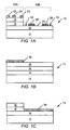
- FIGs. 1A-1C are schematic drawings illustrating examples along with device precursors that may be an intermediate step in the fabrication of a device as illustrated.
- FIGs. 2A-2B are schematic drawings illustrating examples along with a device precursor that may be an intermediate step in the fabrication of a device as illustrated.
- FIGs. 3A-3B are schematic drawings illustrating examples along with a device precursor that may be an intermediate step in the fabrication of a device as illustrated.
- FIG. 4 is a schematic drawing illustrating examples.
- FIG. 5 is a schematic drawing illustrating examples.
- FIGs. 6A-6C are schematic drawings illustrating examples along with a device precursor that may be an intermediate step in the fabrication of a device as illustrated.
- FIG. 7 is a schematic drawing illustrating examples.
- FIG. 8 is a schematic drawing illustrating examples.
- FIG. 9 is a schematic drawing illustrating examples.
- FIG. 10 is a perspective drawing illustrating a conventional surface acoustic wave device.
- FIG. 11 is a schematic drawing illustrating the layout of an interdigital transducer of a conventional surface acoustic wave device.
- FIGs. 12A-12B are schematic illustrations of two device epitaxial structures.
- FIG. 13A is a schematic drawing illustrating examples.
- FIG. 13B is an equivalent circuit diagram of two devices formed on a common substrate according to some examples.
- FIG. 14A-14B are schematic drawings illustrating examples.
- FIG. 15 is a schematic drawing illustrating examples.
- FIG. 16 is a schematic drawing illustrating examples.
- FIGs. 17A-17B are schematic drawings illustrating examples.
- FIG. 18 is a schematic drawing illustrating some embodiments of the present invention along with device precursors that may be an intermediate step in the fabrication of a device as illustrated.
- FIG. 19 is a schematic drawing illustrating some embodiments of the present invention along with device precursors that may be an intermediate step in the fabrication of a device as illustrate
- FIGs. 20A through 20C are schematic drawings illustrating processing steps in the fabrication of devices in accordance with some embodiments of the present invention.
- references herein to a layer formed "on" a substrate or other layer may refer to the layer formed directly on the substrate or other layer or on an intervening layer or layers formed on the substrate or other layer.
- references herein to a layer formed "on" a substrate or other layer may refer to the layer formed directly on the substrate or other layer or on an intervening layer or layers formed on the substrate or other layer.
- first and second elements or layers need not be in direct physical contact with one another, but may be connected by intervening conductive elements or layers which permit current flow between the first and second elements or layers.
- a transistor structure 10A of a device 10 comprises a high electron mobility transistor (HEMT); however, it will be appreciated by those skilled in the art that the transistor structure 10A (as well as the transistor structures illustrated in connection with embodiments of the invention described below) may comprise one or more other types of devices instead of or in addition to a HEMT.
- the transistor structure 10A may comprise a MESFET, MOSFET, JFET or other device.
- the integrated device 10 includes a substrate 12 that may, for example, be silicon carbide (SiC), such as semi-insulating silicon carbide of the 4H polytype.
- SiC silicon carbide
- Other silicon carbide candidate polytypes include the 3C, 6H, and 15R polytypes.
- the term "semi-insulating" is used descriptively rather than in an absolute sense.
- the silicon carbide bulk crystal has a resistivity equal to or higher than about 1x10 5 ⁇ -cm at room temperature.
- An aluminum nitride buffer layer 14 on the substrate 12 provides an appropriate crystal structure transition between the silicon carbide substrate and the remainder of the device.
- the aluminum nitride buffer layer 14 also forms a piezoelectric film on which a SAW device 10B is fabricated as described in more detail below.
- the buffer layer 14 and subsequent GaN-based layers may be formed by MOCVD, MBE, or any other suitable growth technique for forming high-quality epitaxial layers.
- Silicon carbide has a much closer crystal lattice match to Group III nitrides than does sapphire (Al 2 O 3 ), which is a very common substrate material for Group III nitride devices. The closer lattice match may result in Group III nitride films of higher quality than those generally available on sapphire. Silicon carbide also has a very high thermal conductivity so that the total output power of Group III nitride devices on silicon carbide is, typically, not as limited by thermal dissipation of the substrate as in the case of the same devices formed on sapphire. Also, the availability of semi-insulating silicon carbide substrates may provide for device isolation and reduced parasitic capacitance.
- silicon carbide is the preferred substrate material
- embodiments of the present invention may utilize any suitable substrate, such as sapphire, aluminum nitride, aluminum gallium nitride, gallium nitride, silicon, GaAs, LGO, ZnO, LAO, InP and the like.
- an appropriate buffer layer also may be formed.
- Group III nitride refers to those semiconducting compounds formed between nitrogen and the elements in Group III of the periodic table, usually aluminum (Al), gallium (Ga), and/or indium (In).
- the term also refers to ternary and quaternary compounds such as AlGaN and AlInGaN.
- the Group III elements can combine with nitrogen to form binary (e.g., GaN), ternary (e.g., AlGaN, AlInN), and quaternary (e.g., AlInGaN) compounds. These compounds all have empirical formulas in which one mole of nitrogen is combined with a total of one mole of the Group III elements. Accordingly, formulas such as Al x Ga 1-x N where 0 ⁇ x ⁇ 1 or In y Al x Ga 1-x-y N where 0 ⁇ x ⁇ 1, 0 ⁇ y ⁇ 1 and x+y ⁇ 1 are often used to describe them.
- Appropriate semi-insulating SiC substrates are manufactured by, for example, Cree, Inc., of Durham, N.C., the assignee of the present invention, and the methods for producing are described, for example, U. S. Patent Nos. Re. 34,861 ; 4,946,547 ; 5,200,022 ; 6,218,680 ; 6,403,982 ; and 6,396,080 .
- techniques for epitaxial growth of Group III nitrides have been described in, for example, U. S. Patent Nos. 5,210,051 ; 5,393,993 ; 5,523,589 ; and 5,292,501 .
- Suitable structures for GaN-based HEMTs are described, for example, in commonly assigned U.S. Patent 6,316,793 and U.S. application serial no. 09/904,333 filed July 12,2001 for "ALUMINUM GALLIUM NITRIDE/GALLIUM NITRIDE HIGH ELECTRON MOBILITY TRANSISTORS HAVING A GATE CONTACT ON A GALLIUM NITRIDE BASED CAP SEGMENT AND METHODS OF FABRICATING SAME," U.S. provisional application serial no. 60/290,195 filed May 11, 2001 for "GROUP III NITRIDE BASED HIGH ELECTRON MOBILITY TRANSISTOR (HEMT) WITH BARRIER/SPACER LAYER" and United States Patent Application Serial No. 10/102,272, to Smorchkova et al. , entitled “GROUP-III NITRIDE BASED HIGH ELECTRON MOBILITY TRANSISTOR (HEMT) WITH BARRIER/SPACER LAYER”.
- the channel layer 16 is preferably undoped, but may be doped with various substances in order to modify the electron concentration in the sheet charge region or the behavior of the conduction band E c and valence band E v in the area below the sheet charge region.
- the channel layer 16 is about 1 to 5 ⁇ m thick.
- the channel layer 16 may comprise a thick (1 to 5 ⁇ m) GaN-based buffer layer with a thin (approximately 100 ⁇ ) high-quality channel region formed thereon.
- the barrier layer 18 is formed on the channel layer 16.
- the barrier layer 18 may comprise AlGaN, thereby forming a heterojunction between the channel layer 16 and the barrier layer 18.
- the barrier layer 18 preferably has an aluminum composition of between 20% and 40% and may be doped with silicon at a doping concentration of about 2 ⁇ 10 18 cm -3 .
- the barrier layer 18 may be between about 15 nm and 40 nm in thickness, and is preferably about 25 nm thick.
- An ohmic source electrode 22 and an ohmic drain electrode 23 are formed on the surface of the barrier layer 18.
- the source 22 and drain 23 ohmic electrodes may be Ti/Si/Ni, Ti/Al/Ni, Ti/Al/Ni/Au or any other suitable material that forms an ohmic contact to n-type AlGaN.
- Appropriate ohmic contacts for AlGaN/GaN HEMT devices are described in S. T. Sheppard, W. L. Pribble, D. T. Emerson, Z. Ring, R. P.
- the distance between the source electrode 22 and the drain electrode 23 is typically about 2-4 ⁇ m.
- a thin (20-40 A), undoped GaN cap layer may be formed on the surface of the barrier layer 18 between the source 22 and the drain 23 ohmic electrodes.
- the design and effect of such cap layers is described in detail in U.S. Application Ser. No. 09/904,333 to Smith for "ALUMINUM GALLIUM NITRIDE/GALLIUM NITRIDE HIGH ELECTRON MOBILITY TRANSISTORS HAVING A GATE CONTACT ON A GALLIUM NITRIDE BASED CAP SEGMENT AND METHODS OF FABRICATING SAME".
- the gate electrode 24 is formed between the source 22 and the drain 23 electrodes.
- the gate electrode 24 is formed of platinum, nickel or any other suitable metal that forms a non-ohmic contact to n-type Al x Ga 1-x N.
- the gate electrode 24 may be capped with an additional metal layer in a T-gate configuration, or a T-gate may be formed in one process step. As is known in the art, T-gate configurations are particularly suitable for RF and microwave devices.
- the barrier layer 18 may also be provided with multiple layers as described in the above-referenced United States Patent Application Serial No. 10/102,272, to Smorchkova et al.
- embodiments of the present invention should not be construed as limiting the barrier layer to a single layer but may include, for example, barrier layers having combinations of GaN, AlGaN and/or AlN layers.
- barrier layers having combinations of GaN, AlGaN and/or AlN layers.
- a GaN, AlN structure may be utilized to reduce or prevent alloy scattering.
- a first plurality of metal fingers 26 forms an input IDT on the exposed surface 25, while a second plurality of metal fingers 28 forms an output IDT.
- the input IDT 26, the output IDT 28 and the AIN buffer layer 14 form a surface acoustic wave device 10B integrated on the same substrate as the transistor 10A.
- the IDTs 26, 28 may be formed of aluminum or any other suitable metal.
- IDTs 26, 28 do not have to form an ohmic or other electrical contact with the buffer layer 14, many different metals may be employed (including for example the same metals used for the gate 24, the source 22 and drain 23 ohmic contacts and/or metal interconnections to reduce the number of metallization steps required).
- the thickness of the buffer layer 14 affects the SAW propagation characteristics of SAW structure 10B.
- a surface acoustic wave propagating in a device extends for a distance of about one wavelength into the structure.
- the buffer layer is about 250 nm or less.
- the SAW velocity of the propagating wave may be dominated by the SiC substrate, which has a higher SAW velocity than AlN.
- the orientation of the SAW IDT fingers 26, 28 may be chosen so as to optimize the performance of the device.
- SiC MESFETs are typically manufactured using 8° off-axis wafers.
- the input IDT 26 or the output IDT 28 may be connected to the source 22, the drain 23 and/or the gate 24 of transistor 10A via an overlayer metal (not shown), or via wire bonding or any other suitable technique so that electrical signals can be communicated from transistor 10A to SAW device 10B and vice versa.
- the die may be cut at an angle different from the orientation of the IDT fingers 26, 28 as illustrated in FIG. 9 .
- SAW reflectors and/or absorbers 19 may be formed on the device adjacent the input IDT 26 and/or the output IDT 28 to minimize undesired interference.
- the design of SAW reflectors and absorbers is well known to those skilled in the design of SAW devices.
- a precursor device 11 may be formed by depositing epitaxial layers on a substrate 12 to form the buffer layer 14, the channel layer 16 and the barrier layer 18.
- an etch mask 32 is formed on the surface of the barrier layer 18.
- the etch mask 32 may comprise photoresist, silicon dioxide, silicon nitride, or any other suitable mask that permits selective etching of the underlying nitride epitaxial layers.
- the etch mask 32 is patterned using standard photolithography techniques and partially removed.
- a typical photolithography process can include the steps of adding a layer of photoresist (typically a polymer resin sensitive to light) to a semiconductor structure, positioning a mask over the photoresist, exposing the photoresist to a frequency of light to which it responds (by undergoing a chemical change; usually its solubility in a particular solvent), etching the photoresist to remove the exposed or unexposed pattern (depending upon the resist selected), and then carrying out the next desired step on the remaining pattern.
- a layer of photoresist typically a polymer resin sensitive to light
- the barrier and channel layers 16, 18 are then etched away to reveal a portion of the AlN buffer layer 14 on which the IDTs 26, 28 may be formed.
- the etch mask 32 is then removed and metallization steps are performed to form the contacts 22, 23, 24 and the IDTs 26, 28.
- the barrier 16 and the channel 18 layers may be etched using a dry etch process such as reactive ion etching (RIE).
- RIE reactive ion etching
- Suitable conditions for dry etching the mesa may include dry etching in an Ar environment using BCl 3 etchant.
- a typical process may include flowing Ar at 20-100 sccm and BCl 3 at 10-20 sccm in an RIE reactor at a pressure of 5-50 mTorr and an RF power at 50-300W. Actual parameters will depend on the system used and may be determined by those skilled in the art.
- the etch should be highly selective to etch GaN but not AlN.
- the device 10 may be fabricated by placing the substrate 12 into a growth reactor and depositing the AIN buffer layer 14 on the substrate 12 as described above. After formation of the buffer layer 14, the substrate 12 is removed from the growth reactor and a growth mask 34 (which may comprise silicon dioxide, silicon nitride or another suitable material) is formed on the surface of the buffer layer. The mask layer 34 is patterned using standard photolithographic techniques as described above to reveal a portion of the surface of the buffer layer 14. After formation and patterning of the mask layer 34, the substrate 12 is placed back into a growth reactor for the regrowth of channel and the barrier layer 16 and the channel layer 18 (and any other layers that may be present in the device). The contacts 22, 23, 24 and the IDTs 26, 28 may then be formed on the structure after removal of the mask layer 34.
- a growth mask 34 which may comprise silicon dioxide, silicon nitride or another suitable material
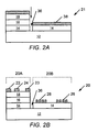
- the device 20 includes a SAW structure 20B that is isolated from a transistor structure 20A by forming a trench 36 between the structures that extends through buffer layer 14.
- the trench 36 may extend into the substrate 12 depending on the thickness of the buffer layer 14 and the wavelength of the device.
- a SAW extends for a distance of about one wavelength into the propagating medium.
- the trench 36 may extend for a distance of at least about one wavelength in order to provide physical isolation of SAW device 20B.
- the trench 36 may be formed before, during or after formation of the transistor.
- an etch mask 38 may be formed on the structure and patterned to reveal a portion of the buffer layer 14 adjacent the transistor mesa. The exposed region is then etched in the manner described above to provide device isolation. After etching, the etch mask is removed and metallization is performed as illustrated in FIG 2 B.
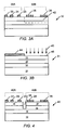
- FIGs. 3A-3B illustrate other examples.
- a device 30 includes a transistor structure 30A and a SAW device structure 30B formed on a common substrate.
- the IDTs 26, 28 of the SAW device 30B are formed on the surface of the same epitaxial layer as the transistor electrodes, thus avoiding the need for regrowth or mesa etching.
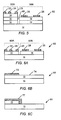
- ions 43 such as nitrogen or phosphorus, are implanted into a region 42 of the device to render the region 42 sufficiently highly resistive as to be electrically inactive.
- a patterned implant mask 44 (which may comprise photoresist) is formed on the surface of the precursor structure 31 and nitrogen ions 43 are implanted into the exposed surface 45 so as to implant the nitrogen ions 43 into the region 42.
- Other ions can be used to increase the resistivity of the region via implantation, including hydrogen, helium, aluminum, nitrogen, magnesium, zinc and/or calcium.
- the implantation can be carried out in a conventional fashion and at room temperature.
- the implanting ions create damage within the GaN to produce deep levels within the bandgap. These in turn trap free carriers in the GaN, thus rendering the material more resistive than a GaN layer or region without such an implant.
- the implanted ions effectively neutralize the conductive 2DEG channel at the interface between the barrier and channel layers.
- nitrogen atoms are implanted into the exposed region at an energy of 10-400 keV and a dosage of 10 13 -10 14 ions per square centimeter (cm -2 ). Such a dose may be sufficient to neutralize the region 42 or otherwise make the region 42 sufficiently non-conductive such that the transistor structure 30A is electrically isolated from the SAW device 30B such that the electrical performance of either the transistor structure 30A or the SAW device 30B are not substantially impaired by the other device.
- FIG. 4 illustrates a device 40 according to further examples.
- a SAW device 40B is formed on the same epitaxial surface as the transistor structure 40A.
- an isolation trench 56 is formed between the SAW structure 40B and the transistor structure 40A using the masking and etching techniques described above in connection with FIGs. 2A and 2B .
- the depth of the trench 56 may be equal to at least one SAW wavelength.
- FIG. 5 Further examples are illustrated in FIG. 5 .
- the barrier and the channel layers of the transistor structure 50A are etched down into the thick GaN layer 16 to remove the 2DEG region between the barrier and channel layers.
- the SAW IDTs are formed on the exposed surface of the GaN layer, which is semi-insulating as grown.
- An optional isolation trench 66 may be etched between the transistor structure 50A and the SAW device structure 50B using the techniques described above.
- an AIN-based SAW structure 60B is integrated on the same substrate as a SiC MESFET structure 60A.
- Techniques for growing epitaxial layers of silicon carbide are disclosed in U.S. Patent Nos. U.S. 6,063,186 ; 6,297,522 ; 6,217,662 ; 5,155,062 ; 4,946,547 ; 4,912,063 ; 4,912,064 ; and 5,011,549 .
- Techniques for growing epitaxial layers of silicon carbide are also disclosed in U.S. Application Serial No. 09/715,576 filed November 17, 2000 for "SUSCEPTOR DESIGNS FOR SILICON CARBIDE THIN FILMS"; U.S. Application Serial No.
- the SiC epitaxial layers 72 may be grown using techniques described in the foregoing patents and applications to form a precursor structure 61 as illustrated in FIG. 6 B.
- An etch mask 73 is formed on the surface of the SiC epitaxial layers 72 and patterned to reveal a portion of the surface 74 of the SiC epitaxial layers 72.
- the precursor structure 61 is then etched to reveal a portion of the semi-insulating SiC substrate.
- the remaining SiC epitaxial layers are then masked with a growth mask 77 illustrated in FIG. 6C that extends just past the edge of the SiC epitaxial layers 72 by a predetermined distance that may depend on the thickness of the growth mask 77.
- the etch mask 73 may or may not be removed prior to formation of the growth mask 77.
- a layer of crystalline AIN 14 is regrown on the exposed substrate and the mask 77 is removed. Because the regrown AIN layer 14 is separated from the SiC epitaxial layer 72, the SAW structure 60B and the MESFET structure 60A are isolated as grown. The metal contacts 22, 23, 24 are formed on the SiC epitaxial layers 72 and the SAW IDTs 26, 28 are then formed on the AIN layer to complete the device.
- the foregoing techniques can be extended to integrate more than one type of device on the same substrate as one or more SAW devices.
- the device 70 includes a transistor structure 70A, a SAW device 70B and a photodetector structure 70C integrated on the same substrate 12.
- Such a device may, for example, be used as a monolithic element capable of receiving, amplifying, and filtering an optical information signal.
- the examples illustrated in FIG. 8 include a transistor structure 80A, a SAW device 80B, a photodetector structure 80C, and an emitter structure 80D integrated on the same substrate 12.
- Such devices may, for example, be used as a monolithic element capable of receiving, amplifying, and filtering an optical information signal and transmitting an information signal.
- the design of GaN-based emitters and photodetectors is well known to those skilled in the art. Examples of GaN-based photodetectors are illustrated in U.S. Patents 6,495,852 and 6,265,727 . Examples of GaN-based emitters are illustrated in U.S. Patents 5,523,589 and 5,739,554 .
- circuit elements may be integrated onto the same substrate as the SAW device and the electronic device.
- capacitors, inductors, resistors, delay lines and the like may be integrated into the device as well.
- nitride devices on a common substrate poses challenges, because many types of devices, such as transistors, emitters, limiters, etc., have complex epitaxial structures which are tailored to the operation of a particular type of device.
- Embodiments of the present invention arise from a recognition that while certain devices have different epitaxial structures, some aspects of those structures may be similar, and may be used in different types of devices formed on a common substrate.
- FIG 12A and FIG. 12B show exemplary epitaxial precursor structures that may be used to form two different types of devices.
- the epitaxial structure shown in FIG. 12A (Type I) may be used to fabricate a low-noise amplifier or a power amplifier, while the epitaxial structure shown in FIG. 12B (Type II) may be used as a basis for a limiter or an RF switch transistor.
- the Type I epitaxial structure of FIG. 12A includes a substrate 100 on which a buffer layer 102 and channel layer 104 are formed.
- the substrate 100 may include a semi-insulating 6H or 4H silicon carbide substrate.
- the buffer layer 102 may include an aluminum nitride layer, which may provide an appropriate crystal structure transition between the silicon carbide substrate 100 and the remainder of the device.
- the buffer layer 102 may be formed by metal-organic chemical vapor deposition and may have a thickness of about 100 ⁇ to about 10,000 ⁇ . In particular embodiments, the buffer layer 102 may have a thickness of about 1000 ⁇ .
- a channel layer 104 which in some examples is semi-insulating Al x Ga 1-x N (0 ⁇ x ⁇ 1), is formed on the buffer layer 102.
- the channel layer 104 is undoped, but in other examples may be doped with various impurities in order to modify the electron concentration in the sheet charge region or the behavior of the conduction band Ec and valence band Ev in the area below the sheet charge region.
- the channel layer 104 is about 1 to 5 ⁇ m thick.
- the channel layer 104 may include a 2 ⁇ m thick-GaN-based buffer layer with a thin (approximately 100 A) high-quality channel region (not shown) formed thereon.
- a barrier layer 106 is formed on the channel layer 104.
- the barrier layer 106 may include AIN, thereby forming a heterojunction between the channel layer 104 and the barrier layer 106.
- a high bandgap layer 108 is on the barrier layer 106.
- the high bandgap layer 108 may include Al x Ga 1-x N (0 ⁇ x ⁇ 1) having an aluminum composition of between 20% and 40%.
- the high bandgap layer 108 may have a higher bandgap than the channel layer 104.
- the high bandgap layer 108 may be doped with silicon at a doping concentration of about 2x10 18 CM -3 .
- the high bandgap layer 108 may be between about 15 nm and 40 nm in thickness, and in some examples is about 25 nm thick.
- a high purity silicon nitride layer 110 may be formed on the high bandgap layer 108.
- High purity silicon nitride may be formed as described in commonly-assigned U.S. Patent Application Serial No. 11/286,805 filed November 23, 2005 and entitled "GROUP III NITRIDE SEMICONDUCTOR DEVICES WITH SILICON NITRIDE LAYERS AND METHODS OF MANUFACTURING SUCH DEVICES".
- the Type I epitaxial structure of FIG. 12A may be useful for forming a HEMT device for a low noise and/or high power amplifier.
- the Type I epitaxial structure may provide appropriate peak current, transconductance, and/or breakdown voltage characteristics useful for high power amplifier output transistors.
- the thickness and/or the aluminum percentage of the high bandgap layer 108 may be adjusted to provide appropriate characteristics for a low noise amplifier.
- the epitaxial structure shown in FIG. 12B (Type II) is similar to the Type I epitaxial structure shown in FIG. 12A , except that the Type II epitaxial structure includes an additional epitaxial layer 112 between the high bandgap layer 108 and the high purity silicon nitride layer 110.
- the high bandgap layer 108, the barrier layer 106 and the channel layer 104 may be the same as in the Type I epitaxial structure.
- the additional epitaxial layer 112 may include a layer of doped GaN and/or graded AlGaN having a thickness of about 300 ⁇ to about 1000 ⁇ .
- the additional epitaxial layer 112 may increase the distance between the top surface of the device and the charge in a 2DEG channel induced at the interface between the channel layer 104 and the barrier layer 106. This may reduce the gate-to-source capacitance of the device, while maintaining a low channel resistance.
- a device having a Type I epitaxial structure and a device having a Type II epitaxial structure may be integrated on a common substrate as illustrated in FIG. 13A .
- a Type II epitaxial structure may be formed using, for example, conventional MOCVD growth techniques.
- Source/drain ohmic contacts 122, 124, 128 may be recessed through the high purity silicon nitride layer 110 and the additional epitaxial layer 112. While not illustrated in FIG. 13A , the source/drain ohmic contacts 122, 124, 128 may be fully and/or partially recessed into/through the high bandgap layer 108 and/or the barrier layer 106.
- a first transistor Q1 is defined by a gate 120 positioned between adjacent source/drain contacts 122, 124.
- the first transistor Q1 may be, for example, a high power or low-noise transistor.
- the gate contact 120 is recessed through both the high purity silicon nitride layer 110 and the additional epitaxial layer 112, as shown in FIG. 13A .
- the gate etch is used to remove a portion, or all, of the additional epitaxial layer 112 underneath the high purity silicon nitride layer 110.
- a low channel or access resistance may be maintained in the non-gated regions of the first transistor Q1 due to the presence of the additional epitaxial layer 112, which, as explained above, may be a relatively thick GaN cap and/or graded/doped AlGaN as described in Journal of Electronic Materials, Vol. 33, No. 5, 2004 , or IEEE Electron Device Letters, Vol. 25, No. 1, January 2004 or Journal Of Applied Physics Volume 94, Number 8, 15 October 2003 ..
- a second transistor Q2 is defined by a second gate contact 126 positioned between source/drain contacts 124, 128.
- the second transistor Q2 may be configured, for example, as a limiter and/or an RF switch.
- the second gate contact 126 may be recessed only through the high purity silicon nitride layer, and is not recessed through, or is only partially recessed through, the additional epitaxial layer 112. The presence of the additional epitaxial layer 112 may reduce the gate capacitance of the second transistor Q2.
- two transistors Q1 and Q2 having different epitaxial structures and/or different operational characteristics, may be provided on the same substrate by forming a single epitaxial structure and etching the structure appropriately.
- FIG. 13 B A schematic diagram of a possible circuit formed by the first and second transistors Q1 and Q2 is illustrated in FIG. 13 B. As shown therein, the first and second transistors may share a common source/drain contact 124.
- FIGs. 14A and 14B Further methods and structures according to examples are illustrated in FIGs. 14A and 14B .
- a Type I epitaxial structure similar to the structure illustrated in FIG. 12A is provided.
- the structure shown in FIG. 14A includes a buffer layer 102 on a substrate 100.
- a channel layer 104, a barrier layer 106, a high bandgap layer 108 and a high purity silicon nitride layer 110 are formed on the buffer layer 102.
- a photoresist mask 210 is formed on a portion of the high purity silicon nitride layer 110, and a portion of the high purity silicon nitride layer exposed by the mask 210 (i.e.
- the mask 210 may be etched away using, for example, conventional dry etching techniques.
- the exposed portions of the high purity silicon nitride layer 110 may be etched away, for example, to reveal the high bandgap layer 108 beneath the high purity silicon nitride layer 110.
- the photoresist mask 210 may be removed, and a epitaxial layer 125 may be epitaxially regrown on the exposed high bandgap layer 108.
- the epitaxial layer 125 may be similar to the epitaxial layer 112 shown in FIG. 13A .
- the epitaxial layer 125 may include doped GaN and/or graded AlGaN, and may have a thickness of about 30 ⁇ to about 10,000 ⁇ .
- the high purity silicon nitride layer 110 may act as a growth mask for the growth of the epitaxial layer 125. That is, when the epitaxial layer 125 is regrown, for example using MOCVD, crystalline material may not nucleate and/or grow on the high purity silicon nitride layer 110, as the high purity silicon nitride layer 110 may not provide a suitable template for epitaxial growth.
- the photoresist mask 210 used as an etch mask when the high purity silicon nitride layer 110 is etched may not be useful as a growth mask, because the polymer-based material used in photoresist may not withstand the high temperatures required for epitaxial growth of nitride materials.
- a separate growth mask may be provided on the high purity silicon nitride layer 110.
- a growth mask 160 may be formed on the high purity silicon nitride layer 110.
- the growth mask may include, for example, silicon dioxide and/or aluminum nitride.
- the growth mask may be formed on the high purity silicon nitride layer 110 prior to etching the high purity silicon nitride layer 110, and may be patterned using conventional lithographic techniques.
- the silicon dioxide should have a thickness greater than 1000 ⁇ .
- the same etch mask 210 may be used to pattern both the etch mask 160 and the high purity silicon nitride layer 110.
- the etch mask 210 may be used to pattern the growth mask 160, and the growth mask 160 may be used as an etch mask for etching the high purity silicon nitride layer 110, as well as for preventing and/or reducing unwanted nucleation on the high purity silicon nitride layer 110 during epitaxial regrowth of the epitaxial layer 125.
- some random crystallite and/or polycrystalline material 163 may nucleate and/or grow on the growth mask 160.
- the unwanted material 163 may be removed by removing the growth mask 160 from the high purity silicon nitride layer 110, which may be done, for example, by performing a buffered oxide etch (BOE) if the growth mask 160 is silicon dioxide.
- BOE buffered oxide etch
- a BOE may etch silicon dioxide but may not etch high purity silicon nitride 110.
- a plurality of devices may be defined in the epitaxial structure by forming one or more electrical contacts on the structure.
- a first transistor Q3 which may be a low noise amplifier and/or a high power amplifier, may be defined by forming source/drain contacts 132, 134 on the high bandgap layer 108.
- the source/drain contacts 132, 134 may be partially and/or fully recessed through the high bandgap layer 108.
- a gate contact 130 for the first transistor Q3 is recessed through the high purity silicon nitride layer 110.
- the transistor Q3 may have an insulating gate structure (e.g.
- MISHFET metal-insulator-semiconductor heterojunction field effect transistor
- a second transistor Q4 may be formed in the region of the structure in which the epitaxial layer 125 was regrown.
- the second transistor Q4 may be defined by a gate contact 140 that is recessed through a silicon nitride layer 170 that may be formed on the epitaxial layer 125.
- Source and drain contacts 142, 144 complete the second transistor Q4.
- the second transistor Q4 may be configured as a two terminal device, such as a limiter diode, by electrically connecting the source contact 142 and the drain contact 144.
- the source and drain contacts 142, 144 together function as a device cathode, while the gate contact 140 may function as a device anode.
- a limiter diode may be used, for example, as an input to an amplifier transistor, such as the first transistor Q3.
- the epitaxial layers of the first transistor Q3 may serve as the substrate on which the epitaxial layers of the second transistor Q4 are formed. Accordingly, some examples provide a first nitride based electronic device including a first nitride based epitaxial structure, and a second nitride based electronic device having a second nitride based epitaxial structure formed on the first nitride based epitaxial structure. In the case of the structure shown in FIG.
- the buffer layer 102, channel layer 104, barrier layer 106 and high bandgap layer 108 form a first epitaxial structure for a first transistor Q3, while the epitaxial layer 125 forms a second epitaxial structure, formed on the first epitaxial structure, for a second transistor Q4.
- the first regrown layer 127 may have a thickness of about 0.5 ⁇ m and a doping concentration of about 2x10 18 cm -3 or more, which provides a surface charge density of at least about 1x10 14 cm -2 .
- the second regrown layer 129 may have a thickness of at least 1000 ⁇ , and may be doped lightly enough that it is fully depleted at zero bias. In particular, the second regrown layer 129 may have a doping concentration of less than about 1x10 16 cm -3 .
- Examples of the present invention may provide both enhancement and depletion mode nitride-based transistor devices on a common substrate.
- a depletion mode device may be formed by providing an epitaxial structure, such as the Type I epitaxial structure shown in FIG. 12A , and forming ohmic contacts thereto as described in connection with FIG. 14C.
- An enhancement mode device may be formed using the same epitaxial structure, but by recessing the gate contact into the underlying high bandgap layer 108 or performing a threshold-voltage shift using negative ions and introducing them into the device by ion implantation or plasma immersion doping.
- Some examples provide for the integration of both silicon carbide devices and nitride devices on a common substrate.
- a silicon carbide MESFET device and a nitride based SAW device may be integrated on a common substrate.
- it may be possible to form an epitaxial layer 72 of silicon carbide on a substrate on which a layer 14 of aluminum nitride is also formed.
- gallium nitride based epitaxial layers are conventionally grown on on-axis substrates, while silicon carbide epitaxial layers are conventionally grown on off-axis substrates, although it is possible to grow relatively thin ( ⁇ 100 nm) epitaxial layers of silicon carbide on an on-axis substrate.
- a silicon carbide MESFET may be formed on an on-axis substrate by implanting source/drain regions as well as a channel region in an on-axis semi-insulating silicon carbide substrate, as illustrated in FIGS. 17A and 17B .
- one or more implant regions may be formed in an on-axis, semi-insulating 4H-SiC substrate by means of ion implantation.
- an n-type channel region 216 may be formed in the substrate 200 by selective implantation of nitrogen and/or phosphorus ions.
- n+ source/drain regions 212, 214 may be formed in the substrate 200 by ion implantation.
- Implantation of dopants into bulk silicon carbide layers is known in the art.
- the dopants may be activated by annealing the implanted structure at a temperature of about 1400 °C to about 1700 °C for about 5 minutes to about 30 minutes.
- the implanted regions of the substrate 200 may then be masked with a growth mask 205.
- the growth mask 205 may include, for example, a SiN and/or SiO 2 pattern formed on the surface of the substrate 200.
- An epitaxial structure 210 may be grown on the exposed portions of the substrate 200 using conventional epitaxial growth techniques.
- the epitaxial structure 210 may include a buffer layer, a channel layer, a barrier layer, and a high bandgap layer, which may have structures similar to the corresponding layers shown, for example, in FIG. 12A , in order to provide an epitaxial precursor for a HEMT device.
- it will be appreciated that other epitaxial structures could be formed, depending on the type/characteristics of nitride device desired.
- the growth mask 205 may be removed, and a passivation layer 228, such as silicon dioxide and/or silicon nitride, may be formed on exposed portions of the substrate 200 and the epitaxial structure 210.
- a passivation layer 228, such as silicon dioxide and/or silicon nitride may be formed on exposed portions of the substrate 200 and the epitaxial structure 210.
- the growth mask may be left on the substrate as a passivation layer, and a second passivation layer may be formed on the nitride epitaxial layers.
- the passivation layer on the nitride epitaxial structure 210 may be different from the passivation layer on the silicon carbide substrate 200.
- the passivation layer 228 may include multiple passivation layers of the same and/or different types of materials stacked on one another.
- a first gate contact 230 and corresponding source/drain contacts 232, 234 may be formed on the epitaxial structure 210 to define a HEMT transistor device Q5, and a second gate contact 240 may be formed on the implanted channel region 216 along with corresponding source/drain contacts 242, 244, to define a silicon carbide MESFET device Q6 in the substrate 200.
- the nitride device Q5 and the silicon carbide device Q6 may be interconnected on the common substrate 200 by one or more levels of interconnect metallization.
- a dielectric layer 260 may be formed on the nitride device Q5 and the silicon carbide device Q6.
- Metal contact plugs 261, 262 may be formed through the dielectric layer 260 to contact electrical contacts of the nitride device Q5 and the silicon carbide device Q6, respectively.
- the contact plugs 261, 262 may be electrically connected, for example, by an overlayer metal 266 formed on the dielectric layer 260. Other connections between the nitride device Q5 and the silicon carbide device Q6 are possible.
- a silicon carbide transistor device may be formed on the same substrate as a nitride-based transistor device to form a monolithically integrated device structure.
- Monolithically integrated nitride devices, and monolithically integrated silicon carbide/nitride devices may have particular applications in monolithic microwave integrated circuits, in which it may be desirable to carefully control the orientation, placement and/or interconnection of devices, due to the high frequency and/or high power of signals processed by such devices.
- Such interconnections may also increase the difficulty of circuit design, since the circuit designer must take into account additional signal delays and/or signal dispersion associated with chip-to-chip interconnections.
- a first device having a first epitaxial structure for example, a low noise and/or high power amplifier (LNA) can be integrated with a second device having a second epitaxial structure (Type II), for example, a limiter diode, according to some examples discussed above.
- Type I a first epitaxial structure
- Type II a second epitaxial structure
- a limiter diode for example, a limiter diode
- Type II structure including a full n + /n - GaN epitaxial structure as discussed above can be selectively grown on top of the Type I epitaxial structure, it may be possible to screen areas of the wafer to maintain the Type I structure while growing the extra layers in the regions of the wafer that require Type II as discussed in detail above.
- devices that include buried, high-conductive regions can be formed by first forming a highly conductive region by selective ion implantation as will be discussed below with respect to FIGs. 18 through 20C .
- a highly conductive region by selective ion implantation as will be discussed below with respect to FIGs. 18 through 20C .
- a buffer layer 102 is provided on a substrate 100.
- a channel layer 104, a barrier layer 106, a high bandgap layer 108 are sequentially provided on the buffer layer 102.
- implanted source and drain regions 801 and 802, respectively, are provided in the high bandgap layer 108 on the Type I side of the integrated device.
- the source and drain regions 801 and 802 may be implanted n + source and drain regions. Details of doping concentrations for these regions are discussed in commonly assigned United States Patent Application No. 11/302,062 to Sheppard et al., filed on December 13, 2005 entitled "SEMICONDUCTOR DEVICES INCLUDING IMPLANTED REGIONS AND PROTECTIVE LAYERS AND METHODS OF FORMING THE SAME.”
- an implanted highly conductive region 805 in accordance with the embodiments of the present invention is provided in the high bandgap layer 108 on the Type II side of the integrated device.
- the highly conductive region 805 may be an implanted n + region having a peak doping concentration of about 5.0X10 20 cm -3 .
- an epitaxially regrown layer 129 of n- GaN is provided on the n + implanted region 805.
- the regrown layer 129 may have a thickness of at least 1000 ⁇ , and may be doped lightly enough that it is fully depleted at zero bias.
- the second regrown layer 129 may have a doping concentration of less than about 1x10 16 cm -3 .
- a plurality of devices may be defined in the epitaxial structure by forming one or more electrical contacts on the structure.
- a first transistor for example, a low noise amplifier and/or a high power amplifier, may be defined by forming source/drain contacts 132, 134 on the implanted n + source and drain regions 801 and 802, respectively, in high bandgap layer 108.
- a gate contact 130 for the first transistor is recessed through the high purity silicon nitride layer 110.
- a second transistor may be formed in the region of the structure in which the epitaxial layer 129 was regrown.
- the second transistor may be defined by a gate contact 140 that is recessed through a silicon nitride layer 170 that may be formed on the epitaxial layer 129.
- Source and drain contacts 142, 144 complete the second transistor.
- the second transistor may be configured as a two terminal device as illustrated in FIG. 19 , such as a limiter diode, by electrically connecting the source contact 142 and the drain contact 144.
- the source and drain contacts 142, 144 together function as a device cathode, while the gate contact 140 may function as a device anode.
- n + implanted region 805 in the bandgap layer 108 allows the regrown region 127 illustrated in FIG. 16 to be reduced.
- the device illustrated in FIG. 18 may be configured as a two terminal device as illustrated in FIG. 19 .
- the anode contact (140) would be placed on a regrown n + layer, which may cause hexagonal pit defects.
- the anode 901 is provide on the epitaxially regrown layer 129 of n - GaN, which is provided on the n + implanted region 805.
- the cathode 902 of the two terminal device is provided on the n + implanted region 805.
- FIGs. 20A through 20C Processing steps in the fabrication of integrated devices in accordance with some embodiments of the present invention will be discussed with respect to FIGs. 20A through 20C .
- the discussion with respect to Figures will be limited to the formation of the implanted source and drain regions 801 and 802, the n + region 805 and the n - GaN layer 129 as the formation of the remaining elements of FIGs. 20A through 20C have been thoroughly discussed herein.
- a mask 1000 for example, SiO 2 may be deposited and patterned on the high bandgap layer 108. Ions are implanted into the portion of the high bandgap layer exposed through the mask 1000 to implant the n + source and drain regions drain regions 801 and 802, respectively.
- the mask 1000 is removed and a second mask 1010, for example, SiO2 may be deposited and patterned on the high bandgap layer 108. Ions are implanted into the portion of the high bandgap layer exposed through the mask 1010 to implant the highly conductive region 805 in accordance with the embodiments of the present invention.
- the highly conductive region 805 may be an implanted n + region may have peak doping concentration of about 5.0x10 20 cm -3 .
- the mask 1010 may be removed and a third mask 1020, for example, SiO2, may be deposited and patterned on the high bandgap layer 108.
- a third mask 1020 for example, SiO2
- the growth mask 1020 may be formed on the high purity silicon nitride layer 108 and may be patterned using conventional lithographic techniques.
- the silicon dioxide may have a thickness greater than about 1000 ⁇ .
- the mask 1010 has been removed in FIG. 20C , in some embodiments of the present invention the growth mask 1020 may be formed with the mask 1010 still in place without departing form the scope of the present invention.
- An epitaxially regrown layer 129 of n - GaN is provided on the n + implanted region 805.
- the regrown layer 129 may have a thickness of at least about 1000 ⁇ , and may be doped lightly enough that it is fully depleted at zero bias.
- the regrown layer 129 may have a doping concentration of less than about 1.0x10 16 cm -3 in some embodiments.
- the masks 1020 and 1010, if present, may be stripped and the device may be finished using conventional techniques.
- the device structures illustrated herein may be representative unit cell structures that are replicated in larger devices, which may have multiple gate fingers on multiple active regions.
- some embodiments of the invention employ semi-insulating silicon carbide substrates, other types and/or conductivities of substrates may be utilized.
Landscapes
- Physics & Mathematics (AREA)
- Acoustics & Sound (AREA)
- Engineering & Computer Science (AREA)
- Manufacturing & Machinery (AREA)
- Junction Field-Effect Transistors (AREA)
Claims (17)
- Monolithische elektronische Vorrichtung, umfassend:eine gemeinsame Nitridepitaxialschicht;eine Nitridvorrichtung erster Art auf der gemeinsamen Nitridepitaxialschicht umfassend einen ersten, wenigstens einen implantierten n-leitenden Bereich auf der gemeinsamen Nitridepitaxialschicht, wobei der erste, wenigstens eine implantierte n-leitende Bereich eine erste Dotierungskonzentration aufweist, welche größer als eine Dotierungskonzentration der gemeinsamen Nitridepitaxialschicht ist;eine sich von der Nitridvorrichtung erster Art unterscheidende Nitridvorrichtung zweiter Art, welche einen zweiten, wenigstens einen implantierten n-leitenden Bereich auf der gemeinsamen Nitridepitaxialschicht umfasst, wobei sich der zweite, wenigstens eine implantierte n-leitende Bereich von dem ersten, wenigstens einen implantierten n-leitenden Bereich unterscheidet und welcher eine zweite Dotierungskonzentration aufweist, die größer als die Dotierungskonzentration der gemeinsamen Nitridepitaxialschicht ist;eine erste Mehrzahl von elektrischen Kontakten auf dem ersten, wenigstens einen implantierten n-leitenden Bereich, wobei die erste Mehrzahl von Kontakten eine erste elektronische Vorrichtung von der Nitridvorrichtung erster Art definiert; undeine zweite Mehrzahl von elektrischen Kontakten auf dem zweiten, wenigstens einen implantierten n-leitenden Bereich, wobei die zweite Mehrzahl von Kontakten eine zweite elektronische Vorrichtung von der zweiten Art von elektronischer Vorrichtung definiert,dadurch gekennzeichnet, dass
der zweite, wenigstens eine implantierte n-leitende Bereich sich auf der gemeinsamen Nitridepitaxialschicht unterhalb allen von der zweiten Mehrzahl von elektrischen Kontakten erstreckt. - Monolithische elektronische Vorrichtung nach Anspruch 1, wobei der erste, wenigstens eine implantierte n-leitende Bereich Source- und Drain-Bereiche für die erste elektronische Vorrichtung umfasst und wobei die erste Mehrzahl von elektrischen Kontakten einen Source-Kontakt auf dem Source-Bereich, einen Drain-Kontakt auf dem Drain-Bereich und einen Gate-Kontakt zwischen den Source- und den Drain-Kontakten umfasst.
- Monolithische elektronische Vorrichtung nach Anspruch 2, wobei der zweite, wenigstens eine implantierte n-leitende Bereich einen sehr leitfähigen n-leitenden Bereich umfasst und wobei die zweite Mehrzahl von elektrischen Kontakten Source- und Drain-Kontakte und einen Gate-Kontakt zwischen den Source- und Drain-Kontakten auf dem sehr leitfähigen n-leitenden Bereich umfasst.
- Monolithische Vorrichtung nach Anspruch 3, wobei der sehr leitfähige n-leitende Bereich eine Dotierungskonzentration von etwa 5,0 x 10¹⁸ bis etwa 6,0 x 1018 cm-3 und eine Tiefe von etwa 0,1 bis etwa 1,0 µm aufweist.
- Monolithische Vorrichtung nach Anspruch 3, wobei die Gate- und Drain-Kontakte der zweiten elektronischen Vorrichtung elektrisch gekoppelt sind, um eine Anode zu bilden.
- Monolithische elektronische Vorrichtung nach Anspruch 3, wobei die gemeinsame Nitridepitaxialstruktur umfasst:eine Nitridkanalschicht;eine Nitridsperrschicht auf der Nitridkanalschicht, wobei die Nitridsperrschicht eine höhere Bandlücke als die Nitridkanalschicht aufweist, wobei die Nitridsperrschicht und der Nitridkanal gemeinsam ein zweidimensionales Elektronengas an einem Übergang zwischen der Nitridkanalschicht und der Nitridsperrschicht induzieren.
- Monolithische elektronische Vorrichtung nach Anspruch 6, ferner umfassend eine hohe Bandlückenschicht auf der Sperrschicht und eine Siliciumnitridschicht auf der hohen Bandlückenschicht.
- Monolithische elektronische Vorrichtung nach Anspruch 7, wobei der sehr leitfähige n-leitende Bereich ein implantierten Bereich von n-leitendem AlxGa1-xN (0≤x≤1) in der hohen Bandlückenschicht umfasst, die zweite elektronische Vorrichtung eine Schicht von n-leitendem AlxGa1-xN (0≤x≤1) auf dem sehr leitfähigen n-leitenden Bereich umfasst, welche eine Dotierungskonzentration von weniger als etwa 1x1016 cm-3 aufweist.
- Monolithische elektronische Vorrichtung nach Anspruch 1, wobei die erste elektronische Vorrichtung einen High Electron Mobility Transistor umfasst und wobei die zweite elektronische Vorrichtung eine/einen von einer akustischen Oberflächenwellenvorrichtung, einer Diode, einem Feldeffekttransistor und einem MISHFET umfasst.
- Monolithische elektronische Vorrichtung, umfassend:eine Nitridepitaxialstruktur umfassend:eine Nitridkanalschicht;eine Nitridsperrschicht auf der Nitridkanalschicht, wobei die Nitridsperrschicht eine höhere Bandlücke als die Nitridkanalschicht aufweist;die Nitridsperrschicht und der Nitridkanal gemeinsam ein zweidimensionales Elektronengas an einem Übergang zwischen der Nitridkanalschicht und der Nitridsperrschicht induzieren;erste und zweite n-leitende implantierte Bereiche auf der Sperrschicht, welche Source- bzw. Drain-Bereiche definieren;eine erste Gate-Elektrode zwischen den Source- und Drain-Bereichen, wobei die erste Gate-Elektrode eine erste Transistorvorrichtung definiert;einen dritten n-leitenden implantierten Bereich auf der Sperrschicht, welcher einen implantierten sehr leitfähigen n-leitenden Bereich definiert; undeine zweite Gate-Elektrode auf dem implantierten sehr leitfähigen n-leitenden Bereich, wobei die zweite Gate-Elektrode eine zweite Transistorvorrichtung definiert.
- Verfahren zum Bilden einer monolithischen elektronischen Vorrichtung, umfassend:Bilden einer gemeinsamen Nitridepitaxialschicht;Bilden einer Nitridvorrichtung erster Art auf der gemeinsamen Nitridepitaxialschicht, einschließlich eines ersten, wenigstens ein implantierten n-leitenden Bereichs auf der gemeinsamen Nitridepitaxialschicht, wobei der erste, wenigstens ein implantierte n-leitende Bereich eine erste Dotierungskonzentration aufweist, welche größer ist als eine Dotierungskonzentration von der gemeinsamen Nitridepitaxialschicht;Bilden einer sich von der Nitridvorrichtung erster Art unterscheidenden Nitridvorrichtung zweiter Art, umfassend einen zweiten, wenigstens einen implantierten n-leitenden Bereich auf der gemeinsamen Nitridepitaxialschicht, wobei sich der zweite, wenigstens eine implantierte n-leitende Bereich von dem ersten, wenigstens einen implantierten n-leitenden Bereich unterscheidet und eine zweite Dotierungskonzentration aufweist, welche größer als die Dotierungskonzentration von der gemeinsamen Nitridepitaxialschicht ist;Bilden einer ersten Mehrzahl von elektrischen Kontakten auf dem ersten, wenigstens einen implantierten n-leitenden Bereich, wobei die erste Mehrzahl von Kontakten eine erste elektronische Vorrichtung von der Nitridvorrichtung erster Art definiert; undBilden einer zweiten Mehrzahl von elektrischen Kontakten auf dem zweiten, wenigstens einen implantierten n-leitenden Bereich, wobei die zweite Mehrzahl von Kontakten eine zweite elektronische Vorrichtung von der zweiten Art von elektronischer Vorrichtung definiert, wobei Bilden der zweiten Mehrzahl von elektronischen Kontakten Bilden der zweiten elektronischen Kontakte auf dem zweiten, wenigstens einen implantierten n-leitenden Bereich umfasst, so dass der zweite, wenigstens eine implantierte n-leitende Bereich sich unterhalb allen von der zweiten Mehrzahl von elektronischen Kontakten erstreckt.
- Verfahren nach Anspruch 11, wobei Bilden des ersten, wenigstens einen implantierten n-leitenden Bereichs Implantieren von Source- und Drain-Bereichen für die erste elektronische Vorrichtung umfasst und wobei Bilden der ersten Mehrzahl von elektrischen Kontakten Bilden eines Source-Kontakts auf dem Source-Bereich, eines Drain-Kontakts auf dem Drain-Bereich und eines Gate-Kontakts zwischen den Source- und den Drain-Kontakten umfasst.
- Verfahren nach Anspruch 12, wobei Bilden des zweiten, wenigstens einen implantierten n-leitenden Bereichs Implantieren eines sehr leitfähigen n-leitenden Bereichs umfasst und wobei Bilden der zweiten Mehrzahl von elektrischen Kontakten Bilden von Source- und Drain-Kontakten und einem Gate-Kontakt zwischen den Source- und Drain-Kontakten auf dem sehr leitfähigen n-leitenden Bereich umfasst.
- Verfahren nach Anspruch 10, wobei Bilden des sehr leitfähigen n-leitenden Bereichs Bilden des sehr leitfähigen n-leitenden Bereichs umfasst, welcher eine Dotierungskonzentration von etwa 5,0 x 10¹⁸ bis etwa 6,0 x 1018 cm-3 und eine Tiefe von etwa 0,1 bis etwa 1,0 µm aufweist.
- Verfahren nach Anspruch 19, wobei Bilden der Gate- und Drain-Kontakte von der zweiten elektronischen Vorrichtung Bilden der Gate- und Drain-Kontakte umfasst, so dass die Gate- und Drain-Kontakte elektrisch gekoppelt sind, um eine Anode zu bilden.
- Verfahren nach Anspruch 14, wobei Bilden der gemeinsamen Nitridepitaxialstruktur umfasst:Bilden einer Nitridkanalschicht;Bilden einer Nitridsperrschicht auf der Nitridkanalschicht, wobei die Nitridsperrschicht eine höhere Bandlücke als die Nitridkanalschicht aufweist, wobei die Nitridsperrschicht und der Nitridkanal gemeinsam ein zweidimensionales Elektronengas an einem Übergang zwischen der Nitridkanalschicht und der Nitridsperrschicht induzieren, wobei das Verfahren ferner umfasst:Bilden einer hohen Bandlückenschicht auf der Sperrschicht und eine Siliciumnitridschicht auf der hohen Bandlückenschicht.
- Verfahren nach Anspruch 16, wobei Bilden des sehr leitfähigen n-leitenden Bereichs Implantieren eines Bereichs von n-leitendem AlxGa1-xN (0≤x≤1) in der hohen Bandlückenschicht umfasst, wobei das Verfahren ferner Bilden einer Schicht von n-leitendem AlxGa1-xN (0≤x≤1) auf dem sehr leitfähigen n-leitenden Bereich umfasst, welcher eine Dotierungskonzentration von weniger als etwa 1 x1016 cm-3 aufweist.
Priority Applications (1)
| Application Number | Priority Date | Filing Date | Title |
|---|---|---|---|
| EP12170574.3A EP2495759B1 (de) | 2008-03-19 | 2009-02-09 | Integrierte auf Nitrid und Siliziumkarbid basierende Baulemente |
Applications Claiming Priority (2)
| Application Number | Priority Date | Filing Date | Title |
|---|---|---|---|
| US12/051,303 US7898047B2 (en) | 2003-03-03 | 2008-03-19 | Integrated nitride and silicon carbide-based devices and methods of fabricating integrated nitride-based devices |
| PCT/US2009/000802 WO2009117045A1 (en) | 2008-03-19 | 2009-02-09 | Integrated nitride and silicon carbide-based devices and methods of fabricating integrated nitride-based devices |
Related Child Applications (2)
| Application Number | Title | Priority Date | Filing Date |
|---|---|---|---|
| EP12170574.3A Division EP2495759B1 (de) | 2008-03-19 | 2009-02-09 | Integrierte auf Nitrid und Siliziumkarbid basierende Baulemente |
| EP12170574.3 Division-Into | 2012-06-01 |
Publications (2)
| Publication Number | Publication Date |
|---|---|
| EP2255387A1 EP2255387A1 (de) | 2010-12-01 |
| EP2255387B1 true EP2255387B1 (de) | 2012-07-11 |
Family
ID=40638004
Family Applications (2)
| Application Number | Title | Priority Date | Filing Date |
|---|---|---|---|
| EP09722679A Active EP2255387B1 (de) | 2008-03-19 | 2009-02-09 | Integrierte vorrichtungen auf nitrid- und siliziumkarbidbasis sowie verfahren zur herstellung integrierter vorrichtungen auf nitridbasis |
| EP12170574.3A Active EP2495759B1 (de) | 2008-03-19 | 2009-02-09 | Integrierte auf Nitrid und Siliziumkarbid basierende Baulemente |
Family Applications After (1)
| Application Number | Title | Priority Date | Filing Date |
|---|---|---|---|
| EP12170574.3A Active EP2495759B1 (de) | 2008-03-19 | 2009-02-09 | Integrierte auf Nitrid und Siliziumkarbid basierende Baulemente |
Country Status (6)
| Country | Link |
|---|---|
| US (2) | US7898047B2 (de) |
| EP (2) | EP2255387B1 (de) |
| JP (1) | JP5479446B2 (de) |
| KR (1) | KR101645740B1 (de) |
| CN (1) | CN101978489B (de) |
| WO (1) | WO2009117045A1 (de) |
Families Citing this family (70)
| Publication number | Priority date | Publication date | Assignee | Title |
|---|---|---|---|---|
| US5306266A (en) * | 1992-12-21 | 1994-04-26 | The Procter & Gamble Company | Flexible spacers for use in disposable absorbent articles |
| US7898047B2 (en) | 2003-03-03 | 2011-03-01 | Samsung Electronics Co., Ltd. | Integrated nitride and silicon carbide-based devices and methods of fabricating integrated nitride-based devices |
| US7112860B2 (en) | 2003-03-03 | 2006-09-26 | Cree, Inc. | Integrated nitride-based acoustic wave devices and methods of fabricating integrated nitride-based acoustic wave devices |
| JP2008311355A (ja) * | 2007-06-13 | 2008-12-25 | Rohm Co Ltd | 窒化物半導体素子 |
| CN102388441B (zh) * | 2009-04-08 | 2014-05-07 | 宜普电源转换公司 | 增强型GaN高电子迁移率晶体管器件及其制备方法 |
| US8748244B1 (en) * | 2010-01-13 | 2014-06-10 | Hrl Laboratories, Llc | Enhancement and depletion mode GaN HMETs on the same substrate |
| US9449833B1 (en) | 2010-06-02 | 2016-09-20 | Hrl Laboratories, Llc | Methods of fabricating self-aligned FETS using multiple sidewall spacers |
| US8946724B1 (en) * | 2010-06-02 | 2015-02-03 | Hrl Laboratories, Llc | Monolithically integrated self-aligned GaN-HEMTs and Schottky diodes and method of fabricating the same |
| JP5584090B2 (ja) * | 2010-10-22 | 2014-09-03 | トランスフォーム・ジャパン株式会社 | Dc−dcコンバータ |
| US8470652B1 (en) * | 2011-05-11 | 2013-06-25 | Hrl Laboratories, Llc | Monolithic integration of group III nitride enhancement layers |
| US20120313111A1 (en) * | 2011-06-07 | 2012-12-13 | Raytheon Company | DIE ALIGNMENT WITH CRYSTALLOGRAPHIC AXES IN GaN-ON-SiC AND OTHER NON-CUBIC MATERIAL SUBSTRATES |
| JP5494622B2 (ja) * | 2011-11-17 | 2014-05-21 | 株式会社豊田中央研究所 | 半導体装置 |
| US10002957B2 (en) * | 2011-12-21 | 2018-06-19 | Power Integrations, Inc. | Shield wrap for a heterostructure field effect transistor |
| US8614447B2 (en) * | 2012-01-30 | 2013-12-24 | International Business Machines Corporation | Semiconductor substrates using bandgap material between III-V channel material and insulator layer |
| US8901606B2 (en) | 2012-04-30 | 2014-12-02 | Avago Technologies General Ip (Singapore) Pte. Ltd. | Pseudomorphic high electron mobility transistor (pHEMT) comprising low temperature buffer layer |
| US9111868B2 (en) | 2012-06-26 | 2015-08-18 | Freescale Semiconductor, Inc. | Semiconductor device with selectively etched surface passivation |
| US10825924B2 (en) | 2012-06-26 | 2020-11-03 | Nxp Usa, Inc. | Semiconductor device with selectively etched surface passivation |
| US8946776B2 (en) | 2012-06-26 | 2015-02-03 | Freescale Semiconductor, Inc. | Semiconductor device with selectively etched surface passivation |
| US10522670B2 (en) | 2012-06-26 | 2019-12-31 | Nxp Usa, Inc. | Semiconductor device with selectively etched surface passivation |
| JP2014086673A (ja) * | 2012-10-26 | 2014-05-12 | Mitsubishi Electric Corp | モノリシック集積回路 |
| US9337799B2 (en) | 2012-11-02 | 2016-05-10 | Qualcomm Mems Technologies, Inc. | Selective tuning of acoustic devices |
| US8853743B2 (en) | 2012-11-16 | 2014-10-07 | Avago Technologies General Ip (Singapore) Pte. Ltd. | Pseudomorphic high electron mobility transistor comprising doped low temperature buffer layer |
| KR101736277B1 (ko) * | 2012-12-12 | 2017-05-17 | 한국전자통신연구원 | 전계 효과 트랜지스터 및 그 제조 방법 |
| US8946779B2 (en) * | 2013-02-26 | 2015-02-03 | Freescale Semiconductor, Inc. | MISHFET and Schottky device integration |
| US9590048B2 (en) * | 2013-10-31 | 2017-03-07 | Infineon Technologies Austria Ag | Electronic device |
| JP2015177067A (ja) * | 2014-03-14 | 2015-10-05 | 株式会社東芝 | 半導体装置 |
| US20150372096A1 (en) * | 2014-06-20 | 2015-12-24 | Ishiang Shih | High Electron Mobility Transistors and Integrated Circuits with Improved Feature Uniformity and Reduced defects for Microwave and Millimetre Wave Applications |
| US9385224B2 (en) * | 2014-08-13 | 2016-07-05 | Northrop Grumman Systems Corporation | Method of forming an integrated multichannel device and single channel device structure |
| KR101750158B1 (ko) * | 2014-12-26 | 2017-06-22 | 타이완 세미콘덕터 매뉴팩쳐링 컴퍼니 리미티드 | Hemt-호환가능 측면 정류기 구조물 |
| US9653516B2 (en) * | 2014-12-30 | 2017-05-16 | Win Semiconductors Corp. | Acoustic wave device structure, integrated structure of power amplifier and acoustic wave device, and fabrication methods thereof |
| TWI572034B (zh) * | 2015-03-26 | 2017-02-21 | 江文章 | III / nitride semiconductor device and method for producing the same |
| US9627473B2 (en) * | 2015-09-08 | 2017-04-18 | Macom Technology Solutions Holdings, Inc. | Parasitic channel mitigation in III-nitride material semiconductor structures |
| US20170069721A1 (en) | 2015-09-08 | 2017-03-09 | M/A-Com Technology Solutions Holdings, Inc. | Parasitic channel mitigation using silicon carbide diffusion barrier regions |
| WO2017071635A1 (en) * | 2015-10-30 | 2017-05-04 | The Hong Kong University Of Science And Technology | Semiconductor device with iii-nitride channel region and silicon carbide drift region |
| CN105655335A (zh) * | 2016-03-11 | 2016-06-08 | 成都海威华芯科技有限公司 | GaAs微电子集成器件 |
| CN105609499B (zh) * | 2016-03-11 | 2018-12-25 | 成都海威华芯科技有限公司 | 一种GaN集成器件 |
| US10170611B1 (en) | 2016-06-24 | 2019-01-01 | Hrl Laboratories, Llc | T-gate field effect transistor with non-linear channel layer and/or gate foot face |
| CN106898547A (zh) * | 2017-03-31 | 2017-06-27 | 成都海威华芯科技有限公司 | 一种GaN声电集成器件的制作方法 |
| KR102381395B1 (ko) * | 2017-09-18 | 2022-04-01 | 한국전기연구원 | 절연 또는 반절연 6H-SiC 기판에 구현된 SiC 반도체 소자 및 그 제조 방법 |
| CN108091657B (zh) * | 2017-12-27 | 2020-05-12 | 中国科学院长春光学精密机械与物理研究所 | 一种非易失性存储器单元、其制备方法及非易失性存储器 |
| US11056483B2 (en) | 2018-01-19 | 2021-07-06 | Macom Technology Solutions Holdings, Inc. | Heterolithic microwave integrated circuits including gallium-nitride devices on intrinsic semiconductor |
| US10950598B2 (en) * | 2018-01-19 | 2021-03-16 | Macom Technology Solutions Holdings, Inc. | Heterolithic microwave integrated circuits including gallium-nitride devices formed on highly doped semiconductor |
| CN108111142B (zh) * | 2018-01-24 | 2020-11-10 | 清华大学 | 一种基于碳化硅衬底/氧化锌或掺杂氧化锌薄膜的声表面波器件及其制备方法 |
| JP7316757B2 (ja) * | 2018-02-23 | 2023-07-28 | ローム株式会社 | 半導体装置 |
| CN108682734B (zh) * | 2018-04-04 | 2019-04-26 | 华南理工大学 | 一种集成外围电路的氮化镓基传感器及其制备方法 |
| US11038023B2 (en) | 2018-07-19 | 2021-06-15 | Macom Technology Solutions Holdings, Inc. | III-nitride material semiconductor structures on conductive silicon substrates |
| US10868162B1 (en) | 2018-08-31 | 2020-12-15 | Hrl Laboratories, Llc | Self-aligned gallium nitride FinFET and method of fabricating the same |
| EP3624179A1 (de) * | 2018-09-13 | 2020-03-18 | IMEC vzw | Integration eines iii-v-bauelements auf einem si-substrat |
| WO2020059765A1 (ja) * | 2018-09-20 | 2020-03-26 | 株式会社村田製作所 | 弾性波装置 |
| CN111371429B (zh) * | 2018-12-26 | 2022-07-12 | 中芯集成电路(宁波)有限公司上海分公司 | 控制电路与声波滤波器的集成方法和集成结构 |
| CN109742143A (zh) * | 2018-12-29 | 2019-05-10 | 苏州汉骅半导体有限公司 | 集成增强型和耗尽型的hemt及其制造方法 |
| CN110380702B (zh) * | 2019-07-25 | 2020-04-10 | 深圳市汇芯通信技术有限公司 | 集成器件制造方法及相关产品 |
| CN110676272A (zh) * | 2019-09-18 | 2020-01-10 | 深圳第三代半导体研究院 | 一种半导体紫外光电探测器 |
| US11038048B2 (en) * | 2019-10-01 | 2021-06-15 | Taiwan Semiconductor Manufacturing Company, Ltd. | Gallium nitride-on-silicon devices |
| KR102721080B1 (ko) * | 2019-10-08 | 2024-10-24 | 삼성전자주식회사 | 반도체 장치, 그 제조 방법 및 이를 포함하는 디스플레이 장치 |
| EP3809457A1 (de) | 2019-10-16 | 2021-04-21 | IMEC vzw | Co-integration von iii-v-bauelementen mit gruppe-iv-bauelementen |
| WO2021090861A1 (ja) * | 2019-11-06 | 2021-05-14 | 株式会社村田製作所 | 弾性波装置 |
| KR102319996B1 (ko) * | 2020-01-03 | 2021-11-01 | (주)와이솔 | 표면탄성파 소자 및 표면탄성파 소자의 제조방법 |
| WO2021195506A1 (en) | 2020-03-26 | 2021-09-30 | Macom Technology Solutions Holdings, Inc. | Microwave integrated circuits including gallium-nitride devices on silicon |
| US11437367B2 (en) * | 2020-04-21 | 2022-09-06 | Qualcomm Incorporated | Heterogeneous integrated wideband high electron mobility transistor power amplifier with a single-crystal acoustic resonator/filter |
| US11769768B2 (en) * | 2020-06-01 | 2023-09-26 | Wolfspeed, Inc. | Methods for pillar connection on frontside and passive device integration on backside of die |
| US11417644B2 (en) * | 2020-06-17 | 2022-08-16 | Macom Technology Solutions Holdings, Inc. | Integration of multiple discrete GaN devices |
| CN112713183B (zh) * | 2020-12-28 | 2022-06-10 | 光华临港工程应用技术研发(上海)有限公司 | 气体传感器的制备方法及气体传感器 |
| US12218202B2 (en) * | 2021-09-16 | 2025-02-04 | Wolfspeed, Inc. | Semiconductor device incorporating a substrate recess |
| CN114497114B (zh) * | 2021-12-28 | 2025-06-27 | 深圳市汇芯通信技术有限公司 | 集成芯片及其制作方法和集成电路 |
| CN115276583A (zh) * | 2022-06-28 | 2022-11-01 | 深圳市汇芯通信技术有限公司 | 一种表面声波滤波器芯片及其制备方法 |
| CN118016662A (zh) * | 2022-11-10 | 2024-05-10 | 联华电子股份有限公司 | 整合制作工艺和结构 |
| US20240395804A1 (en) * | 2023-05-26 | 2024-11-28 | Cambridge Gan Devices Limited | Power semiconductor device comprising a wide bandgap substrate |
| CN117712124B (zh) * | 2024-02-05 | 2024-04-26 | 中国科学院长春光学精密机械与物理研究所 | 一种基于4H-SiC衬底的高性能CMOS器件 |
| CN119153473B (zh) * | 2024-08-27 | 2026-01-23 | 深圳尚阳通科技股份有限公司 | 集成型功率器件及其制造方法 |
Family Cites Families (84)
| Publication number | Priority date | Publication date | Assignee | Title |
|---|---|---|---|---|
| US526267A (en) * | 1894-09-18 | Island | ||
| US1749201A (en) | 1928-05-28 | 1930-03-04 | Paul W Prutzman | Mercury-bromin derivative of fluorescein |
| US3955160A (en) * | 1975-04-30 | 1976-05-04 | Rca Corporation | Surface acoustic wave device |
| JPS58197910A (ja) | 1982-05-14 | 1983-11-17 | Hitachi Ltd | 弾性表面波素子 |
| JPS62260420A (ja) * | 1986-04-28 | 1987-11-12 | シ−メンス、アクチエンゲゼルシヤフト | 集積nmos回路装置 |
| US4866005A (en) * | 1987-10-26 | 1989-09-12 | North Carolina State University | Sublimation of silicon carbide to produce large, device quality single crystals of silicon carbide |
| US4912064A (en) * | 1987-10-26 | 1990-03-27 | North Carolina State University | Homoepitaxial growth of alpha-SiC thin films and semiconductor devices fabricated thereon |
| US4912063A (en) * | 1987-10-26 | 1990-03-27 | North Carolina State University | Growth of beta-sic thin films and semiconductor devices fabricated thereon |
| US5011549A (en) * | 1987-10-26 | 1991-04-30 | North Carolina State University | Homoepitaxial growth of Alpha-SiC thin films and semiconductor devices fabricated thereon |
| US4884001A (en) | 1988-12-13 | 1989-11-28 | United Technologies Corporation | Monolithic electro-acoustic device having an acoustic charge transport device integrated with a transistor |
| US4946547A (en) * | 1989-10-13 | 1990-08-07 | Cree Research, Inc. | Method of preparing silicon carbide surfaces for crystal growth |
| US5210051A (en) * | 1990-03-27 | 1993-05-11 | Cree Research, Inc. | High efficiency light emitting diodes from bipolar gallium nitride |
| US5292501A (en) * | 1990-06-25 | 1994-03-08 | Degenhardt Charles R | Use of a carboxy-substituted polymer to inhibit plaque formation without tooth staining |
| US5200022A (en) * | 1990-10-03 | 1993-04-06 | Cree Research, Inc. | Method of improving mechanically prepared substrate surfaces of alpha silicon carbide for deposition of beta silicon carbide thereon and resulting product |
| US5155062A (en) * | 1990-12-20 | 1992-10-13 | Cree Research, Inc. | Method for silicon carbide chemical vapor deposition using levitated wafer system |
| US5270554A (en) * | 1991-06-14 | 1993-12-14 | Cree Research, Inc. | High power high frequency metal-semiconductor field-effect transistor formed in silicon carbide |
| US5265267A (en) * | 1991-08-29 | 1993-11-23 | Motorola, Inc. | Integrated circuit including a surface acoustic wave transformer and a balanced mixer |
| JPH05183381A (ja) | 1991-12-27 | 1993-07-23 | Nippon Steel Corp | 高周波回路基板および高周波回路素子 |
| DE4219523A1 (de) * | 1992-06-15 | 1993-12-16 | Daimler Benz Ag | Monolithisch integrierter Millimeterwellenschaltkreis und Verfahren zu dessen Herstellung |
| JPH0770736B2 (ja) * | 1993-03-26 | 1995-07-31 | 株式会社ミリウェイブ | 可変容量回路 |
| JPH06303088A (ja) | 1993-04-13 | 1994-10-28 | Nippon Steel Corp | 高周波回路素子 |
| US5925895A (en) | 1993-10-18 | 1999-07-20 | Northrop Grumman Corporation | Silicon carbide power MESFET with surface effect supressive layer |
| US5393993A (en) | 1993-12-13 | 1995-02-28 | Cree Research, Inc. | Buffer structure between silicon carbide and gallium nitride and resulting semiconductor devices |
| US5523589A (en) * | 1994-09-20 | 1996-06-04 | Cree Research, Inc. | Vertical geometry light emitting diode with group III nitride active layer and extended lifetime |
| US5592501A (en) * | 1994-09-20 | 1997-01-07 | Cree Research, Inc. | Low-strain laser structures with group III nitride active layers |
| US5576589A (en) * | 1994-10-13 | 1996-11-19 | Kobe Steel Usa, Inc. | Diamond surface acoustic wave devices |
| JPH10284762A (ja) | 1995-02-16 | 1998-10-23 | Asahi Chem Ind Co Ltd | 表面弾性波を増幅するための積層構造及び増幅器 |
| US5739554A (en) * | 1995-05-08 | 1998-04-14 | Cree Research, Inc. | Double heterojunction light emitting diode with gallium nitride active layer |
| US6217662B1 (en) * | 1997-03-24 | 2001-04-17 | Cree, Inc. | Susceptor designs for silicon carbide thin films |
| JP3047852B2 (ja) * | 1997-04-04 | 2000-06-05 | 松下電器産業株式会社 | 半導体装置 |
| EP0936734A4 (de) * | 1997-07-28 | 2000-10-25 | Toshiba Kk | Akustische oberflächenwellenanordnung und verfahren zu ihrer herstellung |
| US6063186A (en) * | 1997-12-17 | 2000-05-16 | Cree, Inc. | Growth of very uniform silicon carbide epitaxial layers |
| TW398084B (en) | 1998-06-05 | 2000-07-11 | Hewlett Packard Co | Multilayered indium-containing nitride buffer layer for nitride epitaxy |
| US6316793B1 (en) * | 1998-06-12 | 2001-11-13 | Cree, Inc. | Nitride based transistors on semi-insulating silicon carbide substrates |
| AU1100500A (en) * | 1998-09-30 | 2000-04-17 | Cadence Design Systems, Inc. | Block based design methodology |
| US6968514B2 (en) * | 1998-09-30 | 2005-11-22 | Cadence Design Systems, Inc. | Block based design methodology with programmable components |
| KR100316383B1 (ko) * | 1998-10-30 | 2002-02-19 | 윤덕용 | 모노리딕직접회로위에박막또는후막단결정압전소자를집적한단일칩라디오구조및그제조방법 |
| JP3996282B2 (ja) | 1998-11-11 | 2007-10-24 | 三洋電機株式会社 | 炭化珪素半導体装置の製造方法 |
| US6518637B1 (en) * | 1999-04-08 | 2003-02-11 | Wayne State University | Cubic (zinc-blende) aluminum nitride |
| US6396080B2 (en) * | 1999-05-18 | 2002-05-28 | Cree, Inc | Semi-insulating silicon carbide without vanadium domination |
| US6218680B1 (en) * | 1999-05-18 | 2001-04-17 | Cree, Inc. | Semi-insulating silicon carbide without vanadium domination |
| US6265727B1 (en) * | 1999-06-09 | 2001-07-24 | Cree Lighting Company | Solar blind photodiode having an active region with a larger bandgap than one or both if its surrounding doped regions |
| JP2001007379A (ja) * | 1999-06-24 | 2001-01-12 | Sharp Corp | 窒化ガリウム系化合物半導体受光素子 |
| US6300706B1 (en) * | 1999-07-14 | 2001-10-09 | The United States Of America As Represented By The Secretary Of The Army | Compound semiconductor monolithic frequency sources and actuators |
| JP4850993B2 (ja) * | 2000-01-25 | 2012-01-11 | 古河電気工業株式会社 | 半導体装置およびその製造方法 |
| US6596079B1 (en) | 2000-03-13 | 2003-07-22 | Advanced Technology Materials, Inc. | III-V nitride substrate boule and method of making and using the same |
| JP2001267555A (ja) * | 2000-03-22 | 2001-09-28 | Matsushita Electric Ind Co Ltd | 半導体装置及びその製造方法 |
| GB2366104B (en) * | 2000-05-01 | 2002-10-23 | Murata Manufacturing Co | Surface acoustic wave device, shear bulk wave transducer, and longitudinal bulk wave transducer |
| US6686616B1 (en) * | 2000-05-10 | 2004-02-03 | Cree, Inc. | Silicon carbide metal-semiconductor field effect transistors |
| US6555946B1 (en) * | 2000-07-24 | 2003-04-29 | Motorola, Inc. | Acoustic wave device and process for forming the same |
| US6548333B2 (en) | 2000-12-01 | 2003-04-15 | Cree, Inc. | Aluminum gallium nitride/gallium nitride high electron mobility transistors having a gate contact on a gallium nitride based cap segment |
| US6569250B2 (en) * | 2001-01-08 | 2003-05-27 | Cree, Inc. | Gas-driven rotation apparatus and method for forming silicon carbide layers |
| US6828879B2 (en) * | 2001-02-16 | 2004-12-07 | Sanyo Electric Co., Ltd. | Longitudinal coupled multiple mode surface acoustic wave filter |
| JP3648462B2 (ja) * | 2001-04-27 | 2005-05-18 | 沖電気工業株式会社 | 弾性表面波分波器 |
| US6849882B2 (en) * | 2001-05-11 | 2005-02-01 | Cree Inc. | Group-III nitride based high electron mobility transistor (HEMT) with barrier/spacer layer |
| US6706114B2 (en) * | 2001-05-21 | 2004-03-16 | Cree, Inc. | Methods of fabricating silicon carbide crystals |
| EP1278120A1 (de) * | 2001-07-18 | 2003-01-22 | Infineon Technologies AG | Controller und Verfahren zum Ansteuern einer zentralen Verarbeitungseinheit für eine Speicheradressierung |
| CA2454269C (en) * | 2001-07-24 | 2015-07-07 | Primit Parikh | Insulating gate algan/gan hemt |
| US20030022412A1 (en) * | 2001-07-25 | 2003-01-30 | Motorola, Inc. | Monolithic semiconductor-piezoelectric device structures and electroacoustic charge transport devices |
| US20030030119A1 (en) * | 2001-08-13 | 2003-02-13 | Motorola, Inc. | Structure and method for improved piezo electric coupled component integrated devices |
| JP3733420B2 (ja) * | 2002-03-01 | 2006-01-11 | 独立行政法人産業技術総合研究所 | 窒化物半導体材料を用いたヘテロ接合電界効果型トランジスタ |
| US6797069B2 (en) * | 2002-04-08 | 2004-09-28 | Cree, Inc. | Gas driven planetary rotation apparatus and methods for forming silicon carbide layers |
| US6936869B2 (en) * | 2002-07-09 | 2005-08-30 | International Rectifier Corporation | Heterojunction field effect transistors using silicon-germanium and silicon-carbon alloys |
| US20040136241A1 (en) * | 2002-10-31 | 2004-07-15 | Lockheed Martin Corporation | Pipeline accelerator for improved computing architecture and related system and method |
| US7898047B2 (en) | 2003-03-03 | 2011-03-01 | Samsung Electronics Co., Ltd. | Integrated nitride and silicon carbide-based devices and methods of fabricating integrated nitride-based devices |
| US7112860B2 (en) * | 2003-03-03 | 2006-09-26 | Cree, Inc. | Integrated nitride-based acoustic wave devices and methods of fabricating integrated nitride-based acoustic wave devices |
| US7064359B2 (en) | 2003-08-20 | 2006-06-20 | Matsushita Electric Industrial Co., Ltd. | Switching semiconductor device and switching circuit |
| US7045404B2 (en) * | 2004-01-16 | 2006-05-16 | Cree, Inc. | Nitride-based transistors with a protective layer and a low-damage recess and methods of fabrication thereof |
| US7975094B2 (en) * | 2004-04-15 | 2011-07-05 | Marvell International Technology Ltd. | Programmable I/O interface |
| US7202528B2 (en) * | 2004-12-01 | 2007-04-10 | Semisouth Laboratories, Inc. | Normally-off integrated JFET power switches in wide bandgap semiconductors and methods of making |
| CN1914786B (zh) | 2004-08-26 | 2012-02-08 | 松下电器产业株式会社 | 变换器模块 |
| KR100616621B1 (ko) * | 2004-09-24 | 2006-08-28 | 삼성전기주식회사 | 질화물계 반도체 장치 및 그 제조 방법 |
| JP2006100645A (ja) * | 2004-09-30 | 2006-04-13 | Furukawa Electric Co Ltd:The | GaN系半導体集積回路 |
| US7265399B2 (en) * | 2004-10-29 | 2007-09-04 | Cree, Inc. | Asymetric layout structures for transistors and methods of fabricating the same |
| JP2006148546A (ja) | 2004-11-19 | 2006-06-08 | Eudyna Devices Inc | 増幅回路及びその制御方法、並びに増幅回路モジュール |
| US20070018199A1 (en) * | 2005-07-20 | 2007-01-25 | Cree, Inc. | Nitride-based transistors and fabrication methods with an etch stop layer |
| US7548112B2 (en) * | 2005-07-21 | 2009-06-16 | Cree, Inc. | Switch mode power amplifier using MIS-HEMT with field plate extension |
| US7419892B2 (en) * | 2005-12-13 | 2008-09-02 | Cree, Inc. | Semiconductor devices including implanted regions and protective layers and methods of forming the same |
| US7569466B2 (en) * | 2005-12-16 | 2009-08-04 | International Business Machines Corporation | Dual metal gate self-aligned integration |
| US20070221953A1 (en) * | 2006-03-24 | 2007-09-27 | Kozo Sakamoto | Semiconductor device |
| JP5040170B2 (ja) * | 2006-05-17 | 2012-10-03 | 三菱電機株式会社 | 半導体装置の製造方法 |
| US20080197422A1 (en) * | 2007-02-20 | 2008-08-21 | National Central University | Planar combined structure of a bipolar junction transistor and N-type/P-type metal semiconductor field-effect transistors and method for forming the same |
| MX378120B (es) | 2015-10-16 | 2025-03-10 | O&M Halyard Int Unlimited Co | Metodo y sistema para cortar y colocar tiras metalicas adaptables en un proceso de fabricacion de mascarillas. |
| CN111370594B (zh) | 2020-03-19 | 2023-04-07 | 重庆京东方显示技术有限公司 | 显示面板和显示装置 |
-
2008
- 2008-03-19 US US12/051,303 patent/US7898047B2/en not_active Expired - Lifetime
-
2009
- 2009-02-09 EP EP09722679A patent/EP2255387B1/de active Active
- 2009-02-09 CN CN200980109627.8A patent/CN101978489B/zh active Active
- 2009-02-09 EP EP12170574.3A patent/EP2495759B1/de active Active
- 2009-02-09 WO PCT/US2009/000802 patent/WO2009117045A1/en not_active Ceased
- 2009-02-09 JP JP2011500766A patent/JP5479446B2/ja active Active
- 2009-02-09 KR KR1020107023218A patent/KR101645740B1/ko active Active
-
2011
- 2011-02-28 US US13/036,657 patent/US8035111B2/en not_active Expired - Lifetime
Also Published As
| Publication number | Publication date |
|---|---|
| JP2011514689A (ja) | 2011-05-06 |
| CN101978489B (zh) | 2014-07-02 |
| CN101978489A (zh) | 2011-02-16 |
| EP2495759A1 (de) | 2012-09-05 |
| KR20110002033A (ko) | 2011-01-06 |
| JP5479446B2 (ja) | 2014-04-23 |
| US20080169474A1 (en) | 2008-07-17 |
| US7898047B2 (en) | 2011-03-01 |
| EP2495759B1 (de) | 2014-05-14 |
| US20110147762A1 (en) | 2011-06-23 |
| US8035111B2 (en) | 2011-10-11 |
| EP2255387A1 (de) | 2010-12-01 |
| WO2009117045A1 (en) | 2009-09-24 |
| KR101645740B1 (ko) | 2016-08-04 |
Similar Documents
| Publication | Publication Date | Title |
|---|---|---|
| EP2255387B1 (de) | Integrierte vorrichtungen auf nitrid- und siliziumkarbidbasis sowie verfahren zur herstellung integrierter vorrichtungen auf nitridbasis | |
| US7875910B2 (en) | Integrated nitride and silicon carbide-based devices | |
| EP1747589B1 (de) | Verfahren zur herstellung von transistoren auf nitridbasis mit wiederaufgewachsenen ohmschen kontaktregionen und transistoren auf nitridbasis mit wiederaufgewachsenen ohmschen kontaktregionen | |
| JP5350585B2 (ja) | ミリメートル波動作のための窒化物ベースのトランジスタ | |
| EP2161754A2 (de) | Halbleitervorrichtung und Verfahren zu ihrer Herstellung | |
| TW201209895A (en) | Fabrication of single or multiple gate field plates | |
| CN1989601A (zh) | 制造具有盖层和凹进栅极的氮化物基晶体管的方法 | |
| JP2014003301A (ja) | 窒化物ベースのトランジスタおよびエッチストップ層を用いた製造方法 | |
| CA2456662A1 (en) | High electron mobility devices | |
| US20220109064A1 (en) | Semiconductor materials and devices including iii-nitride layers integrated with scandium aluminum nitride | |
| WO2023286307A1 (ja) | 半導体装置、半導体モジュール及び電子機器 | |
| JP7770424B2 (ja) | 修正アクセス領域を備える電界効果トランジスタ | |
| WO2025109870A1 (ja) | 半導体装置、半導体モジュール及び電子機器 | |
| KR20040046479A (ko) | 반도체 소자의 제조 방법 | |
| WO2024220067A1 (en) | Iii-n dual gate devices | |
| KR20230137469A (ko) | 3족-질화물 고-전자이동도 트랜지스터 및 그 제조 방법 |
Legal Events
| Date | Code | Title | Description |
|---|---|---|---|
| PUAI | Public reference made under article 153(3) epc to a published international application that has entered the european phase |
Free format text: ORIGINAL CODE: 0009012 |
|
| 17P | Request for examination filed |
Effective date: 20100903 |
|
| AK | Designated contracting states |
Kind code of ref document: A1 Designated state(s): AT BE BG CH CY CZ DE DK EE ES FI FR GB GR HR HU IE IS IT LI LT LU LV MC MK MT NL NO PL PT RO SE SI SK TR |
|
| AX | Request for extension of the european patent |
Extension state: AL BA RS |
|
| DAX | Request for extension of the european patent (deleted) | ||
| REG | Reference to a national code |
Ref country code: DE Ref legal event code: R079 Ref document number: 602009008225 Country of ref document: DE Free format text: PREVIOUS MAIN CLASS: H01L0021825200 Ipc: H01L0021820000 |
|
| GRAP | Despatch of communication of intention to grant a patent |
Free format text: ORIGINAL CODE: EPIDOSNIGR1 |
|
| RIC1 | Information provided on ipc code assigned before grant |
Ipc: H03H 9/05 20060101ALI20111213BHEP Ipc: H01L 21/8252 20060101ALI20111213BHEP Ipc: H01L 21/82 20060101AFI20111213BHEP Ipc: H01L 27/20 20060101ALI20111213BHEP Ipc: H01L 21/8258 20060101ALI20111213BHEP Ipc: H01L 27/06 20060101ALI20111213BHEP Ipc: H01L 29/778 20060101ALI20111213BHEP Ipc: H03H 3/08 20060101ALI20111213BHEP Ipc: H03H 9/02 20060101ALI20111213BHEP |
|
| GRAS | Grant fee paid |
Free format text: ORIGINAL CODE: EPIDOSNIGR3 |
|
| GRAA | (expected) grant |
Free format text: ORIGINAL CODE: 0009210 |
|
| AK | Designated contracting states |
Kind code of ref document: B1 Designated state(s): AT BE BG CH CY CZ DE DK EE ES FI FR GB GR HR HU IE IS IT LI LT LU LV MC MK MT NL NO PL PT RO SE SI SK TR |
|
| REG | Reference to a national code |
Ref country code: GB Ref legal event code: FG4D |
|
| REG | Reference to a national code |
Ref country code: CH Ref legal event code: EP |
|
| REG | Reference to a national code |
Ref country code: AT Ref legal event code: REF Ref document number: 566501 Country of ref document: AT Kind code of ref document: T Effective date: 20120715 |
|
| REG | Reference to a national code |
Ref country code: DE Ref legal event code: R082 Ref document number: 602009008225 Country of ref document: DE |
|
| REG | Reference to a national code |
Ref country code: NL Ref legal event code: T3 |
|
| REG | Reference to a national code |
Ref country code: IE Ref legal event code: FG4D |
|
| REG | Reference to a national code |
Ref country code: DE Ref legal event code: R096 Ref document number: 602009008225 Country of ref document: DE Effective date: 20120913 |
|
| REG | Reference to a national code |
Ref country code: AT Ref legal event code: MK05 Ref document number: 566501 Country of ref document: AT Kind code of ref document: T Effective date: 20120711 |
|
| REG | Reference to a national code |
Ref country code: LT Ref legal event code: MG4D Effective date: 20120711 |
|
| PG25 | Lapsed in a contracting state [announced via postgrant information from national office to epo] |
Ref country code: IS Free format text: LAPSE BECAUSE OF FAILURE TO SUBMIT A TRANSLATION OF THE DESCRIPTION OR TO PAY THE FEE WITHIN THE PRESCRIBED TIME-LIMIT Effective date: 20121111 Ref country code: AT Free format text: LAPSE BECAUSE OF FAILURE TO SUBMIT A TRANSLATION OF THE DESCRIPTION OR TO PAY THE FEE WITHIN THE PRESCRIBED TIME-LIMIT Effective date: 20120711 Ref country code: HR Free format text: LAPSE BECAUSE OF FAILURE TO SUBMIT A TRANSLATION OF THE DESCRIPTION OR TO PAY THE FEE WITHIN THE PRESCRIBED TIME-LIMIT Effective date: 20120711 Ref country code: NO Free format text: LAPSE BECAUSE OF FAILURE TO SUBMIT A TRANSLATION OF THE DESCRIPTION OR TO PAY THE FEE WITHIN THE PRESCRIBED TIME-LIMIT Effective date: 20121011 Ref country code: CY Free format text: LAPSE BECAUSE OF FAILURE TO SUBMIT A TRANSLATION OF THE DESCRIPTION OR TO PAY THE FEE WITHIN THE PRESCRIBED TIME-LIMIT Effective date: 20120711 Ref country code: FI Free format text: LAPSE BECAUSE OF FAILURE TO SUBMIT A TRANSLATION OF THE DESCRIPTION OR TO PAY THE FEE WITHIN THE PRESCRIBED TIME-LIMIT Effective date: 20120711 Ref country code: BE Free format text: LAPSE BECAUSE OF FAILURE TO SUBMIT A TRANSLATION OF THE DESCRIPTION OR TO PAY THE FEE WITHIN THE PRESCRIBED TIME-LIMIT Effective date: 20120711 Ref country code: LT Free format text: LAPSE BECAUSE OF FAILURE TO SUBMIT A TRANSLATION OF THE DESCRIPTION OR TO PAY THE FEE WITHIN THE PRESCRIBED TIME-LIMIT Effective date: 20120711 |
|
| PG25 | Lapsed in a contracting state [announced via postgrant information from national office to epo] |
Ref country code: PT Free format text: LAPSE BECAUSE OF FAILURE TO SUBMIT A TRANSLATION OF THE DESCRIPTION OR TO PAY THE FEE WITHIN THE PRESCRIBED TIME-LIMIT Effective date: 20121112 Ref country code: PL Free format text: LAPSE BECAUSE OF FAILURE TO SUBMIT A TRANSLATION OF THE DESCRIPTION OR TO PAY THE FEE WITHIN THE PRESCRIBED TIME-LIMIT Effective date: 20120711 Ref country code: LV Free format text: LAPSE BECAUSE OF FAILURE TO SUBMIT A TRANSLATION OF THE DESCRIPTION OR TO PAY THE FEE WITHIN THE PRESCRIBED TIME-LIMIT Effective date: 20120711 Ref country code: SI Free format text: LAPSE BECAUSE OF FAILURE TO SUBMIT A TRANSLATION OF THE DESCRIPTION OR TO PAY THE FEE WITHIN THE PRESCRIBED TIME-LIMIT Effective date: 20120711 Ref country code: GR Free format text: LAPSE BECAUSE OF FAILURE TO SUBMIT A TRANSLATION OF THE DESCRIPTION OR TO PAY THE FEE WITHIN THE PRESCRIBED TIME-LIMIT Effective date: 20121012 Ref country code: SE Free format text: LAPSE BECAUSE OF FAILURE TO SUBMIT A TRANSLATION OF THE DESCRIPTION OR TO PAY THE FEE WITHIN THE PRESCRIBED TIME-LIMIT Effective date: 20120711 |
|
| PLBI | Opposition filed |
Free format text: ORIGINAL CODE: 0009260 |
|
| PG25 | Lapsed in a contracting state [announced via postgrant information from national office to epo] |
Ref country code: DK Free format text: LAPSE BECAUSE OF FAILURE TO SUBMIT A TRANSLATION OF THE DESCRIPTION OR TO PAY THE FEE WITHIN THE PRESCRIBED TIME-LIMIT Effective date: 20120711 Ref country code: ES Free format text: LAPSE BECAUSE OF FAILURE TO SUBMIT A TRANSLATION OF THE DESCRIPTION OR TO PAY THE FEE WITHIN THE PRESCRIBED TIME-LIMIT Effective date: 20121022 Ref country code: RO Free format text: LAPSE BECAUSE OF FAILURE TO SUBMIT A TRANSLATION OF THE DESCRIPTION OR TO PAY THE FEE WITHIN THE PRESCRIBED TIME-LIMIT Effective date: 20120711 Ref country code: CZ Free format text: LAPSE BECAUSE OF FAILURE TO SUBMIT A TRANSLATION OF THE DESCRIPTION OR TO PAY THE FEE WITHIN THE PRESCRIBED TIME-LIMIT Effective date: 20120711 Ref country code: EE Free format text: LAPSE BECAUSE OF FAILURE TO SUBMIT A TRANSLATION OF THE DESCRIPTION OR TO PAY THE FEE WITHIN THE PRESCRIBED TIME-LIMIT Effective date: 20120711 |
|
| 26 | Opposition filed |
Opponent name: INFINEON TECHNOLOGIES AUSTRIA AG Effective date: 20130411 |
|
| PLAX | Notice of opposition and request to file observation + time limit sent |
Free format text: ORIGINAL CODE: EPIDOSNOBS2 |
|
| PG25 | Lapsed in a contracting state [announced via postgrant information from national office to epo] |
Ref country code: SK Free format text: LAPSE BECAUSE OF FAILURE TO SUBMIT A TRANSLATION OF THE DESCRIPTION OR TO PAY THE FEE WITHIN THE PRESCRIBED TIME-LIMIT Effective date: 20120711 Ref country code: IT Free format text: LAPSE BECAUSE OF FAILURE TO SUBMIT A TRANSLATION OF THE DESCRIPTION OR TO PAY THE FEE WITHIN THE PRESCRIBED TIME-LIMIT Effective date: 20120711 |
|
| REG | Reference to a national code |
Ref country code: DE Ref legal event code: R026 Ref document number: 602009008225 Country of ref document: DE Effective date: 20130411 |
|
| PG25 | Lapsed in a contracting state [announced via postgrant information from national office to epo] |
Ref country code: BG Free format text: LAPSE BECAUSE OF FAILURE TO SUBMIT A TRANSLATION OF THE DESCRIPTION OR TO PAY THE FEE WITHIN THE PRESCRIBED TIME-LIMIT Effective date: 20121011 |
|
| PLAF | Information modified related to communication of a notice of opposition and request to file observations + time limit |
Free format text: ORIGINAL CODE: EPIDOSCOBS2 |
|
| PG25 | Lapsed in a contracting state [announced via postgrant information from national office to epo] |
Ref country code: MC Free format text: LAPSE BECAUSE OF NON-PAYMENT OF DUE FEES Effective date: 20130228 |
|
| REG | Reference to a national code |
Ref country code: CH Ref legal event code: PL |
|
| PG25 | Lapsed in a contracting state [announced via postgrant information from national office to epo] |
Ref country code: CH Free format text: LAPSE BECAUSE OF NON-PAYMENT OF DUE FEES Effective date: 20130228 Ref country code: LI Free format text: LAPSE BECAUSE OF NON-PAYMENT OF DUE FEES Effective date: 20130228 |
|
| REG | Reference to a national code |
Ref country code: FR Ref legal event code: ST Effective date: 20131031 |
|
| PLBB | Reply of patent proprietor to notice(s) of opposition received |
Free format text: ORIGINAL CODE: EPIDOSNOBS3 |
|
| REG | Reference to a national code |
Ref country code: IE Ref legal event code: MM4A |
|
| PG25 | Lapsed in a contracting state [announced via postgrant information from national office to epo] |
Ref country code: IE Free format text: LAPSE BECAUSE OF NON-PAYMENT OF DUE FEES Effective date: 20130209 Ref country code: FR Free format text: LAPSE BECAUSE OF NON-PAYMENT OF DUE FEES Effective date: 20130228 |
|
| PG25 | Lapsed in a contracting state [announced via postgrant information from national office to epo] |
Ref country code: MT Free format text: LAPSE BECAUSE OF FAILURE TO SUBMIT A TRANSLATION OF THE DESCRIPTION OR TO PAY THE FEE WITHIN THE PRESCRIBED TIME-LIMIT Effective date: 20120711 |
|
| REG | Reference to a national code |
Ref country code: DE Ref legal event code: R100 Ref document number: 602009008225 Country of ref document: DE |
|
| PLCK | Communication despatched that opposition was rejected |
Free format text: ORIGINAL CODE: EPIDOSNREJ1 |
|
| PLBN | Opposition rejected |
Free format text: ORIGINAL CODE: 0009273 |
|
| STAA | Information on the status of an ep patent application or granted ep patent |
Free format text: STATUS: OPPOSITION REJECTED |
|
| 27O | Opposition rejected |
Effective date: 20141127 |
|
| PG25 | Lapsed in a contracting state [announced via postgrant information from national office to epo] |
Ref country code: TR Free format text: LAPSE BECAUSE OF FAILURE TO SUBMIT A TRANSLATION OF THE DESCRIPTION OR TO PAY THE FEE WITHIN THE PRESCRIBED TIME-LIMIT Effective date: 20120711 |
|
| PG25 | Lapsed in a contracting state [announced via postgrant information from national office to epo] |
Ref country code: HU Free format text: LAPSE BECAUSE OF FAILURE TO SUBMIT A TRANSLATION OF THE DESCRIPTION OR TO PAY THE FEE WITHIN THE PRESCRIBED TIME-LIMIT; INVALID AB INITIO Effective date: 20090209 Ref country code: MK Free format text: LAPSE BECAUSE OF FAILURE TO SUBMIT A TRANSLATION OF THE DESCRIPTION OR TO PAY THE FEE WITHIN THE PRESCRIBED TIME-LIMIT Effective date: 20120711 Ref country code: LU Free format text: LAPSE BECAUSE OF NON-PAYMENT OF DUE FEES Effective date: 20130209 |
|
| REG | Reference to a national code |
Ref country code: DE Ref legal event code: R079 Ref document number: 602009008225 Country of ref document: DE Free format text: PREVIOUS MAIN CLASS: H01L0021820000 Ipc: H10D0089000000 |
|
| PGFP | Annual fee paid to national office [announced via postgrant information from national office to epo] |
Ref country code: DE Payment date: 20250227 Year of fee payment: 17 |
|
| PGFP | Annual fee paid to national office [announced via postgrant information from national office to epo] |
Ref country code: GB Payment date: 20250227 Year of fee payment: 17 |
|
| PGFP | Annual fee paid to national office [announced via postgrant information from national office to epo] |
Ref country code: NL Payment date: 20260226 Year of fee payment: 18 |