EP2249631A1 - Mehrschichtige leiterplatte und motorantriebsleiterplatte - Google Patents
Mehrschichtige leiterplatte und motorantriebsleiterplatte Download PDFInfo
- Publication number
- EP2249631A1 EP2249631A1 EP09708156A EP09708156A EP2249631A1 EP 2249631 A1 EP2249631 A1 EP 2249631A1 EP 09708156 A EP09708156 A EP 09708156A EP 09708156 A EP09708156 A EP 09708156A EP 2249631 A1 EP2249631 A1 EP 2249631A1
- Authority
- EP
- European Patent Office
- Prior art keywords
- wiring
- circuit board
- multilayer circuit
- wirings
- conductor layers
- Prior art date
- Legal status (The legal status is an assumption and is not a legal conclusion. Google has not performed a legal analysis and makes no representation as to the accuracy of the status listed.)
- Granted
Links
Images



Classifications
-
- H—ELECTRICITY
- H05—ELECTRIC TECHNIQUES NOT OTHERWISE PROVIDED FOR
- H05K—PRINTED CIRCUITS; CASINGS OR CONSTRUCTIONAL DETAILS OF ELECTRIC APPARATUS; MANUFACTURE OF ASSEMBLAGES OF ELECTRICAL COMPONENTS
- H05K1/00—Printed circuits
- H05K1/02—Details
- H05K1/0213—Electrical arrangements not otherwise provided for
- H05K1/0216—Reduction of cross-talk, noise or electromagnetic interference
- H05K1/0228—Compensation of cross-talk by a mutually correlated lay-out of printed circuit traces, e.g. for compensation of cross-talk in mounted connectors
-
- B—PERFORMING OPERATIONS; TRANSPORTING
- B62—LAND VEHICLES FOR TRAVELLING OTHERWISE THAN ON RAILS
- B62D—MOTOR VEHICLES; TRAILERS
- B62D5/00—Power-assisted or power-driven steering
- B62D5/04—Power-assisted or power-driven steering electrical, e.g. using an electric servo-motor connected to, or forming part of, the steering gear
- B62D5/0403—Power-assisted or power-driven steering electrical, e.g. using an electric servo-motor connected to, or forming part of, the steering gear characterised by constructional features, e.g. common housing for motor and gear box
- B62D5/0406—Power-assisted or power-driven steering electrical, e.g. using an electric servo-motor connected to, or forming part of, the steering gear characterised by constructional features, e.g. common housing for motor and gear box including housing for electronic control unit
-
- H—ELECTRICITY
- H02—GENERATION; CONVERSION OR DISTRIBUTION OF ELECTRIC POWER
- H02M—APPARATUS FOR CONVERSION BETWEEN AC AND AC, BETWEEN AC AND DC, OR BETWEEN DC AND DC, AND FOR USE WITH MAINS OR SIMILAR POWER SUPPLY SYSTEMS; CONVERSION OF DC OR AC INPUT POWER INTO SURGE OUTPUT POWER; CONTROL OR REGULATION THEREOF
- H02M7/00—Conversion of AC power input into DC power output; Conversion of DC power input into AC power output
- H02M7/003—Constructional details, e.g. physical layout, assembly, wiring or busbar connections
-
- H—ELECTRICITY
- H02—GENERATION; CONVERSION OR DISTRIBUTION OF ELECTRIC POWER
- H02M—APPARATUS FOR CONVERSION BETWEEN AC AND AC, BETWEEN AC AND DC, OR BETWEEN DC AND DC, AND FOR USE WITH MAINS OR SIMILAR POWER SUPPLY SYSTEMS; CONVERSION OF DC OR AC INPUT POWER INTO SURGE OUTPUT POWER; CONTROL OR REGULATION THEREOF
- H02M1/00—Details of apparatus for conversion
- H02M1/44—Circuits or arrangements for compensating for electromagnetic interference in converters or inverters
-
- H—ELECTRICITY
- H05—ELECTRIC TECHNIQUES NOT OTHERWISE PROVIDED FOR
- H05K—PRINTED CIRCUITS; CASINGS OR CONSTRUCTIONAL DETAILS OF ELECTRIC APPARATUS; MANUFACTURE OF ASSEMBLAGES OF ELECTRICAL COMPONENTS
- H05K1/00—Printed circuits
- H05K1/02—Details
- H05K1/0213—Electrical arrangements not otherwise provided for
- H05K1/0263—High current adaptations, e.g. printed high current conductors or using auxiliary non-printed means; Fine and coarse circuit patterns on one circuit board
-
- H—ELECTRICITY
- H05—ELECTRIC TECHNIQUES NOT OTHERWISE PROVIDED FOR
- H05K—PRINTED CIRCUITS; CASINGS OR CONSTRUCTIONAL DETAILS OF ELECTRIC APPARATUS; MANUFACTURE OF ASSEMBLAGES OF ELECTRICAL COMPONENTS
- H05K1/00—Printed circuits
- H05K1/02—Details
- H05K1/0296—Conductive pattern lay-out details not covered by sub groups H05K1/02 - H05K1/0295
- H05K1/0298—Multilayer circuits
-
- H—ELECTRICITY
- H05—ELECTRIC TECHNIQUES NOT OTHERWISE PROVIDED FOR
- H05K—PRINTED CIRCUITS; CASINGS OR CONSTRUCTIONAL DETAILS OF ELECTRIC APPARATUS; MANUFACTURE OF ASSEMBLAGES OF ELECTRICAL COMPONENTS
- H05K2201/00—Indexing scheme relating to printed circuits covered by H05K1/00
- H05K2201/09—Shape and layout
- H05K2201/09209—Shape and layout details of conductors
- H05K2201/09654—Shape and layout details of conductors covering at least two types of conductors provided for in H05K2201/09218 - H05K2201/095
- H05K2201/09672—Superposed layout, i.e. in different planes
-
- H—ELECTRICITY
- H05—ELECTRIC TECHNIQUES NOT OTHERWISE PROVIDED FOR
- H05K—PRINTED CIRCUITS; CASINGS OR CONSTRUCTIONAL DETAILS OF ELECTRIC APPARATUS; MANUFACTURE OF ASSEMBLAGES OF ELECTRICAL COMPONENTS
- H05K2201/00—Indexing scheme relating to printed circuits covered by H05K1/00
- H05K2201/10—Details of components or other objects attached to or integrated in a printed circuit board
- H05K2201/10007—Types of components
- H05K2201/10166—Transistor
-
- H—ELECTRICITY
- H10—SEMICONDUCTOR DEVICES; ELECTRIC SOLID-STATE DEVICES NOT OTHERWISE PROVIDED FOR
- H10W—GENERIC PACKAGES, INTERCONNECTIONS, CONNECTORS OR OTHER CONSTRUCTIONAL DETAILS OF DEVICES COVERED BY CLASS H10
- H10W72/00—Interconnections or connectors in packages
- H10W72/50—Bond wires
- H10W72/541—Dispositions of bond wires
- H10W72/5445—Dispositions of bond wires being orthogonal to a side surface of the chip, e.g. parallel arrangements
-
- H—ELECTRICITY
- H10—SEMICONDUCTOR DEVICES; ELECTRIC SOLID-STATE DEVICES NOT OTHERWISE PROVIDED FOR
- H10W—GENERIC PACKAGES, INTERCONNECTIONS, CONNECTORS OR OTHER CONSTRUCTIONAL DETAILS OF DEVICES COVERED BY CLASS H10
- H10W72/00—Interconnections or connectors in packages
- H10W72/50—Bond wires
- H10W72/541—Dispositions of bond wires
- H10W72/547—Dispositions of multiple bond wires
- H10W72/5475—Dispositions of multiple bond wires multiple bond wires connected to common bond pads at both ends of the wires
Definitions
- a motor drive circuit board for an electric power steering system comprising: a multilayer circuit board which includes a plurality of conductor layers and a plurality of resin insulation layers which are laminated alternately; a first wiring formed on a first layer of the plurality of conductor layers; and a second wiring formed on a second layer of the plurality of conductor layers, wherein portions of the first wiring and the second wiring which face each other in a direction in which the plurality of conductor layers are laminated extend in parallel; and wherein the first wiring and the second wiring are arranged so as to weaken a magnetic field generated by a current which flows through the first wiring and a magnetic field generated by a current which flows through the second wiring to each other.
- Fig. 1 is an external plan view of a multilayer circuit board according to one embodiment of the invention
- Fig. 2 is an external plan view of the multilayer circuit board with those other than components and wirings which are included in the circuit board made transparent
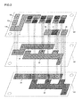
- Fig. 3 is an exploded perspective view showing respective constructions of layers of the multilayer circuit board.
- Fig. 4 is a circuit diagram of the motor drive circuit.
- drain terminals of the MOSFETs 15u, 15v, 15w which are included in the motor drive circuit are connected to positive poles of the power source, not shown, and source terminals thereof are connected to the corresponding phase input terminals of the motor, respectively.
- Source terminals of the MOSFETs 16u, 16v, 16w which are included in the motor drive circuit are connected to the negative pole (the ground pole) of the power source, not shown, via the resistor 17, and drain terminals thereof are connected to the corresponding phase input terminals of the motor, respectively.
- a connecting relationship of the motor drive circuit shown in Fig. 4 corresponds to a connecting relationship between the respective layers shown in Fig. 3 .
- dotted lines extending in a vertical direction in Fig. 3 denote positions of through holes. Since conductor layers (typically, copper plated layers) are formed on inner faces of the through holes, energization or electrical communication is established between the conductors linked to both ends of the through holes. Consequently, as is shown in the circuit diagram in Fig.
- the ground wiring 22 and the power source wiring 33 are disposed so that most of the wirings are superposed vertically.
- the inductance of these wirings is reduced. Namely, since the ground wiring 22 is connected to the ground terminal 20 in the vicinity of a rightward lower end portion in the figure (via the through hole and the resistor 17), a current flows therethrough from the right towards the left of the figure. Consequently, the currents flow in an opposite direction to each other along the direction of the longer side in the portions of the ground wiring 22 and the power source wiring 33 which are superposed. Therefore, since magnetic fields generated by these currents are canceled by each other (namely, since a mutual inductance becomes large), the inductance of these wirings which generally extend long from the terminals can be reduced.
- a multilayer circuit board such as the multilayer circuit boards 100, 110 described above may be used.
- This heat dissipating land 312 is brought into press contact with a projecting portion 302 which is formed underneath an upper gear housing 301 via a heat conduction sheet 321.
- heat of the CPU 330 is transferred to the upper gear housing 301 having a large heat capacity.
- the heat of the CPU 330 is dissipated with good efficiency.
- a configuration may be adopted in which in place of the heat conduction sheet 321, a gel containing a material having heat conduction properties may be applied.
- the CPU 330 has been described as representing an element having a large heat capacity, and this heat dissipating configuration may be applied to other electronic components.
- the configuration in question may be adopted for the MOSFETs 15u, 15v, 15w, 16u, 16v, 16w which are provided on the multilayer circuit boards 100, 110 described above.
- Fig. 9 is a schematic sectional view showing configurations of a bare chip and a non-contacting heat sink.
- a bare chip 450 is mounted on an electronic circuit board 403, and a normal heat sink 404 is attached to a rear face (a lower face in the figure) of the electronic circuit board 403.
- a coating resin 402 is applied to the periphery of the bare chip 405, and a non-contacting heat sink 401 is disposed directly above the bare chip 405 in a closest position so as to face the bare chip 405.
- This non-contacting heat sink 401 is fixed to a housing having a larger heat capacity.
- the invention can provide the multilayer circuit board in which the wirings are arranged so that the inductance thereof is reduced and a motor drive circuit board employing the multilayer circuit board which is used in an electric power steering system.
Landscapes
- Engineering & Computer Science (AREA)
- Physics & Mathematics (AREA)
- Electromagnetism (AREA)
- Microelectronics & Electronic Packaging (AREA)
- Chemical & Material Sciences (AREA)
- Combustion & Propulsion (AREA)
- Transportation (AREA)
- Mechanical Engineering (AREA)
- Power Engineering (AREA)
- Power Steering Mechanism (AREA)
- Structure Of Printed Boards (AREA)
Applications Claiming Priority (2)
| Application Number | Priority Date | Filing Date | Title |
|---|---|---|---|
| JP2008028111A JP5444619B2 (ja) | 2008-02-07 | 2008-02-07 | 多層回路基板およびモータ駆動回路基板 |
| PCT/JP2009/051943 WO2009099131A1 (ja) | 2008-02-07 | 2009-02-05 | 多層回路基板およびモータ駆動回路基板 |
Publications (3)
| Publication Number | Publication Date |
|---|---|
| EP2249631A1 true EP2249631A1 (de) | 2010-11-10 |
| EP2249631A4 EP2249631A4 (de) | 2014-06-25 |
| EP2249631B1 EP2249631B1 (de) | 2017-12-27 |
Family
ID=40952204
Family Applications (1)
| Application Number | Title | Priority Date | Filing Date |
|---|---|---|---|
| EP09708156.6A Not-in-force EP2249631B1 (de) | 2008-02-07 | 2009-02-05 | Mehrschichtige leiterplatte und motorantriebsleiterplatte |
Country Status (5)
| Country | Link |
|---|---|
| US (1) | US8288658B2 (de) |
| EP (1) | EP2249631B1 (de) |
| JP (1) | JP5444619B2 (de) |
| CN (1) | CN101940071B (de) |
| WO (1) | WO2009099131A1 (de) |
Cited By (2)
| Publication number | Priority date | Publication date | Assignee | Title |
|---|---|---|---|---|
| EP3352362A4 (de) * | 2015-09-18 | 2019-05-15 | Mitsubishi Electric Corporation | Integrierte elektrische servolenkvorrichtung |
| EP3487274A1 (de) * | 2017-11-20 | 2019-05-22 | Valeo Comfort and Driving Assistance | Elektronische vorrichtung mit einem strukturellen teil mit einem käfig, der pber einer elektronischen komponente positioniert ist |
Families Citing this family (31)
| Publication number | Priority date | Publication date | Assignee | Title |
|---|---|---|---|---|
| KR101385094B1 (ko) * | 2007-09-11 | 2014-04-14 | 삼성디스플레이 주식회사 | 인쇄회로기판, 이를 갖는 표시장치 및 이의 제조방법 |
| JP5039171B2 (ja) | 2010-05-11 | 2012-10-03 | 三菱電機株式会社 | 電動式駆動装置およびその電動式駆動装置を搭載した電動式パワーステアリング装置 |
| WO2012056735A1 (ja) | 2010-10-27 | 2012-05-03 | 三菱電機株式会社 | 電動パワーステアリング用モータ駆動制御装置 |
| EP2557666B1 (de) * | 2011-08-10 | 2020-05-20 | LG Innotek Co., Ltd. | EPS-Motor |
| JP6075128B2 (ja) * | 2013-03-11 | 2017-02-08 | 株式会社ジェイテクト | 駆動回路装置 |
| US10080301B2 (en) | 2013-10-17 | 2018-09-18 | Cree, Inc. | High voltage power chip module |
| US9389656B2 (en) * | 2014-01-30 | 2016-07-12 | Asia Vital Components Co., Ltd. | Heat dissipation structure applied to mobile device |
| US20150221576A1 (en) * | 2014-01-31 | 2015-08-06 | Asia Vital Components Co., Ltd. | Heat Dissipation Structure for Semiconductor Element |
| CN104022695A (zh) * | 2014-06-23 | 2014-09-03 | 济南科亚电子科技有限公司 | 一种双有刷直流驱动器 |
| US9839146B2 (en) | 2015-10-20 | 2017-12-05 | Cree, Inc. | High voltage power module |
| JP6672747B2 (ja) * | 2015-11-30 | 2020-03-25 | 株式会社ニコン | 電子ユニット、撮像装置及びフレキシブル基板 |
| CN106364551A (zh) * | 2016-10-21 | 2017-02-01 | 杭州飞越汽车零部件有限公司 | 采用嵌入式多层电路板eps控制器的动力总成 |
| JP7422542B2 (ja) * | 2016-12-15 | 2024-01-26 | サン・ディエゴ・ステート・ユニバーシティ・リサーチ・ファンデーション | 局在的配電ネットワーク設計のための重なり合わない電源/グランドプレーン |
| US10008411B2 (en) * | 2016-12-15 | 2018-06-26 | Infineon Technologies Ag | Parallel plate waveguide for power circuits |
| US10410952B2 (en) | 2016-12-15 | 2019-09-10 | Infineon Technologies Ag | Power semiconductor packages having a substrate with two or more metal layers and one or more polymer-based insulating layers for separating the metal layers |
| JP2018148693A (ja) * | 2017-03-06 | 2018-09-20 | 日立オートモティブシステムズ株式会社 | 電動モータの駆動制御装置 |
| JP6729474B2 (ja) * | 2017-04-24 | 2020-07-22 | 三菱電機株式会社 | 半導体装置 |
| US10522442B2 (en) * | 2017-06-29 | 2019-12-31 | Performance Motion Devices, Inc. | Dissipating heat from an electronic device in a protective housing |
| JP6549200B2 (ja) * | 2017-10-03 | 2019-07-24 | 三菱電機株式会社 | 電力変換回路 |
| JP6779193B2 (ja) * | 2017-11-07 | 2020-11-04 | 日立オートモティブシステムズ株式会社 | 電動駆動装置 |
| JP6490255B1 (ja) * | 2018-01-16 | 2019-03-27 | 三菱電機株式会社 | 車載電子装置 |
| USD908632S1 (en) | 2018-09-17 | 2021-01-26 | Cree Fayetteville, Inc. | Power module |
| JP7172849B2 (ja) * | 2019-05-17 | 2022-11-16 | 株式会社デンソー | 電力変換装置 |
| JP7136023B2 (ja) * | 2019-07-01 | 2022-09-13 | 株式会社豊田自動織機 | 回路基板及び回路基板モジュール |
| US10959323B1 (en) | 2019-09-06 | 2021-03-23 | Performance Motion Devices, Inc. | Over-torque protection features for mounting an electronic device to a heat dissipation object |
| JP7215402B2 (ja) * | 2019-11-28 | 2023-01-31 | 株式会社豊田自動織機 | 半導体装置 |
| CN115039518B (zh) * | 2020-01-31 | 2025-09-23 | 发那科株式会社 | 电动机驱动装置及其制造方法 |
| CN113346752B (zh) * | 2020-07-03 | 2025-02-18 | 广东工业大学 | 一种基于氮化镓器件的隔离型高频双有源桥变换器 |
| JP7518776B2 (ja) * | 2021-01-21 | 2024-07-18 | 株式会社Soken | 多層基板 |
| JP7519312B2 (ja) * | 2021-02-09 | 2024-07-19 | Tdk株式会社 | キャパシタ部品 |
| JP7730752B2 (ja) * | 2021-12-24 | 2025-08-28 | Astemo株式会社 | 電子回路基板 |
Family Cites Families (28)
| Publication number | Priority date | Publication date | Assignee | Title |
|---|---|---|---|---|
| JPH04310315A (ja) | 1991-04-09 | 1992-11-02 | Mitsubishi Electric Corp | 放電加工用電源装置 |
| JP2854757B2 (ja) * | 1992-06-17 | 1999-02-03 | 三菱電機株式会社 | 半導体パワーモジュール |
| JP3684239B2 (ja) * | 1995-01-10 | 2005-08-17 | 株式会社 日立製作所 | 低emi電子機器 |
| JPH09181407A (ja) | 1995-12-25 | 1997-07-11 | Sony Tektronix Corp | 回路基板 |
| JP3732927B2 (ja) * | 1997-07-31 | 2006-01-11 | 京セラ株式会社 | 多層配線基板 |
| JP3535827B2 (ja) * | 1997-10-01 | 2004-06-07 | カヤバ工業株式会社 | 電動パワーステアリング装置の電動モータ |
| JPH11152050A (ja) | 1997-11-21 | 1999-06-08 | Kayaba Ind Co Ltd | 電動パワーステアリング装置 |
| JP3595163B2 (ja) * | 1998-05-26 | 2004-12-02 | 松下電器産業株式会社 | 電子機器 |
| JP3552549B2 (ja) * | 1998-09-08 | 2004-08-11 | 株式会社豊田自動織機 | 半導体モジュールの電極端子接続構造 |
| JP3795687B2 (ja) * | 1998-12-15 | 2006-07-12 | 三菱電機株式会社 | 大電流回路基板 |
| JP3644835B2 (ja) * | 1999-01-18 | 2005-05-11 | 三菱電機株式会社 | 電動式パワーステアリング回路装置 |
| JP3692906B2 (ja) * | 2000-05-25 | 2005-09-07 | 日産自動車株式会社 | 電力配線構造及び半導体装置 |
| JP4475757B2 (ja) | 2000-07-19 | 2010-06-09 | 京セラ株式会社 | インバータ制御モジュール |
| JP2002094246A (ja) * | 2000-09-13 | 2002-03-29 | Minebea Co Ltd | 多層プリント配線基板及び多層プリント配線基板の実装方法 |
| JP3774624B2 (ja) | 2000-10-18 | 2006-05-17 | 三菱電機株式会社 | 電動パワーステアリング装置 |
| JP3614380B2 (ja) | 2001-05-17 | 2005-01-26 | 三菱電機株式会社 | 電動式パワーステアリング装置 |
| US6420778B1 (en) * | 2001-06-01 | 2002-07-16 | Aralight, Inc. | Differential electrical transmission line structures employing crosstalk compensation and related methods |
| US6765298B2 (en) * | 2001-12-08 | 2004-07-20 | National Semiconductor Corporation | Substrate pads with reduced impedance mismatch and methods to fabricate substrate pads |
| JP3638269B2 (ja) * | 2002-03-14 | 2005-04-13 | 三菱電機株式会社 | 電動式パワーステアリング装置 |
| JP2005064028A (ja) | 2003-08-12 | 2005-03-10 | Ngk Spark Plug Co Ltd | 配線基板 |
| JP4479522B2 (ja) * | 2005-02-02 | 2010-06-09 | 株式会社デンソー | 電子装置 |
| KR100799839B1 (ko) | 2005-03-30 | 2008-01-31 | 삼성전기주식회사 | 파장변환용 형광체 혼합물과 이를 이용한 백색 발광장치 |
| JP4327774B2 (ja) * | 2005-07-21 | 2009-09-09 | 富士ネームプレート株式会社 | プリント配線板及びその製造方法 |
| JP4333675B2 (ja) * | 2006-01-12 | 2009-09-16 | 株式会社デンソー | インバータ装置用配線基板 |
| WO2007080748A1 (ja) * | 2006-01-16 | 2007-07-19 | Mitsubishi Electric Corporation | 電動機の駆動回路及び空気調和機の室外機 |
| JP4353951B2 (ja) * | 2006-03-06 | 2009-10-28 | 三菱電機株式会社 | 電動式パワーステアリング装置 |
| JP4209904B2 (ja) * | 2006-06-16 | 2009-01-14 | 三菱電機株式会社 | 多層基板 |
| JP4962228B2 (ja) * | 2006-12-26 | 2012-06-27 | 株式会社ジェイテクト | 多層回路基板およびモータ駆動回路基板 |
-
2008
- 2008-02-07 JP JP2008028111A patent/JP5444619B2/ja not_active Expired - Fee Related
-
2009
- 2009-02-05 EP EP09708156.6A patent/EP2249631B1/de not_active Not-in-force
- 2009-02-05 US US12/866,638 patent/US8288658B2/en not_active Expired - Fee Related
- 2009-02-05 WO PCT/JP2009/051943 patent/WO2009099131A1/ja not_active Ceased
- 2009-02-05 CN CN2009801048927A patent/CN101940071B/zh not_active Expired - Fee Related
Cited By (4)
| Publication number | Priority date | Publication date | Assignee | Title |
|---|---|---|---|---|
| EP3352362A4 (de) * | 2015-09-18 | 2019-05-15 | Mitsubishi Electric Corporation | Integrierte elektrische servolenkvorrichtung |
| US10759467B2 (en) | 2015-09-18 | 2020-09-01 | Mitsubishi Electric Corporation | Integrated electric power steering apparatus |
| EP3487274A1 (de) * | 2017-11-20 | 2019-05-22 | Valeo Comfort and Driving Assistance | Elektronische vorrichtung mit einem strukturellen teil mit einem käfig, der pber einer elektronischen komponente positioniert ist |
| WO2019097063A1 (en) * | 2017-11-20 | 2019-05-23 | Valeo Comfort And Driving Assistance | Electronic device comprising a structural piece with a cage positionned over an electronic component |
Also Published As
| Publication number | Publication date |
|---|---|
| CN101940071A (zh) | 2011-01-05 |
| EP2249631B1 (de) | 2017-12-27 |
| JP5444619B2 (ja) | 2014-03-19 |
| JP2009188271A (ja) | 2009-08-20 |
| EP2249631A4 (de) | 2014-06-25 |
| WO2009099131A1 (ja) | 2009-08-13 |
| CN101940071B (zh) | 2012-10-03 |
| US20110011633A1 (en) | 2011-01-20 |
| US8288658B2 (en) | 2012-10-16 |
Similar Documents
| Publication | Publication Date | Title |
|---|---|---|
| US8288658B2 (en) | Multilayer circuit board and motor drive circuit board | |
| CN107408871B (zh) | 电动驱动装置以及电动动力转向装置 | |
| CN107431418B (zh) | 电动驱动装置以及电动动力转向装置 | |
| JP6444495B2 (ja) | 電動パワーステアリング駆動装置 | |
| JP4909961B2 (ja) | 電動パワーステアリング用制御装置 | |
| DE112015006036B4 (de) | Motorantriebs-steuerungseinrichtung für eine elektrische servolenkung | |
| US10136555B2 (en) | Power conversion apparatus having a metal plate for heat dissipation | |
| CN107004649B (zh) | 电子部件搭载用散热基板 | |
| JP6294195B2 (ja) | 電力変換装置 | |
| US10763729B2 (en) | Electronic control unit, and electric power steering device using the same | |
| US10800444B2 (en) | Electric driving device and electric power steering device | |
| JP5397417B2 (ja) | 半導体装置、および、それを用いた駆動装置 | |
| US8520394B2 (en) | Control device | |
| US10249558B2 (en) | Electronic part mounting heat-dissipating substrate | |
| JP6863875B2 (ja) | 電動駆動装置及び電動パワーステアリング装置 | |
| JP2018061363A (ja) | モータ駆動装置、モータシステム及び電動パワーステアリング装置 | |
| CN115206911A (zh) | 电路基板 | |
| JP2014057514A (ja) | 駆動装置 | |
| US9066429B2 (en) | Control device and vehicle steering system including control device | |
| EP2635096B1 (de) | Steuereinheit für Elektromotor und Fahrzeuglenksystem damit | |
| EP2166824A1 (de) | Mehrschichtleiterplatte und Motorantriebsleiterplatte | |
| JP4209904B2 (ja) | 多層基板 | |
| JP7296205B2 (ja) | 配線基板、及び電動駆動装置 |
Legal Events
| Date | Code | Title | Description |
|---|---|---|---|
| PUAI | Public reference made under article 153(3) epc to a published international application that has entered the european phase |
Free format text: ORIGINAL CODE: 0009012 |
|
| 17P | Request for examination filed |
Effective date: 20100805 |
|
| AK | Designated contracting states |
Kind code of ref document: A1 Designated state(s): AT BE BG CH CY CZ DE DK EE ES FI FR GB GR HR HU IE IS IT LI LT LU LV MC MK MT NL NO PL PT RO SE SI SK TR |
|
| AX | Request for extension of the european patent |
Extension state: AL BA RS |
|
| DAX | Request for extension of the european patent (deleted) | ||
| A4 | Supplementary search report drawn up and despatched |
Effective date: 20140528 |
|
| RIC1 | Information provided on ipc code assigned before grant |
Ipc: H05K 1/02 20060101AFI20140521BHEP Ipc: B62D 5/04 20060101ALI20140521BHEP Ipc: H02M 7/00 20060101ALI20140521BHEP |
|
| GRAP | Despatch of communication of intention to grant a patent |
Free format text: ORIGINAL CODE: EPIDOSNIGR1 |
|
| RIC1 | Information provided on ipc code assigned before grant |
Ipc: H02M 7/00 20060101ALI20170815BHEP Ipc: H05K 1/02 20060101AFI20170815BHEP Ipc: B62D 5/04 20060101ALI20170815BHEP Ipc: H02M 1/44 20070101ALN20170815BHEP |
|
| INTG | Intention to grant announced |
Effective date: 20170830 |
|
| GRAS | Grant fee paid |
Free format text: ORIGINAL CODE: EPIDOSNIGR3 |
|
| GRAA | (expected) grant |
Free format text: ORIGINAL CODE: 0009210 |
|
| AK | Designated contracting states |
Kind code of ref document: B1 Designated state(s): AT BE BG CH CY CZ DE DK EE ES FI FR GB GR HR HU IE IS IT LI LT LU LV MC MK MT NL NO PL PT RO SE SI SK TR |
|
| REG | Reference to a national code |
Ref country code: GB Ref legal event code: FG4D Ref country code: FR Ref legal event code: PLFP Year of fee payment: 10 |
|
| REG | Reference to a national code |
Ref country code: CH Ref legal event code: EP |
|
| REG | Reference to a national code |
Ref country code: AT Ref legal event code: REF Ref document number: 959378 Country of ref document: AT Kind code of ref document: T Effective date: 20180115 |
|
| REG | Reference to a national code |
Ref country code: IE Ref legal event code: FG4D |
|
| REG | Reference to a national code |
Ref country code: DE Ref legal event code: R096 Ref document number: 602009050075 Country of ref document: DE |
|
| PG25 | Lapsed in a contracting state [announced via postgrant information from national office to epo] |
Ref country code: NO Free format text: LAPSE BECAUSE OF FAILURE TO SUBMIT A TRANSLATION OF THE DESCRIPTION OR TO PAY THE FEE WITHIN THE PRESCRIBED TIME-LIMIT Effective date: 20180327 Ref country code: FI Free format text: LAPSE BECAUSE OF FAILURE TO SUBMIT A TRANSLATION OF THE DESCRIPTION OR TO PAY THE FEE WITHIN THE PRESCRIBED TIME-LIMIT Effective date: 20171227 Ref country code: LT Free format text: LAPSE BECAUSE OF FAILURE TO SUBMIT A TRANSLATION OF THE DESCRIPTION OR TO PAY THE FEE WITHIN THE PRESCRIBED TIME-LIMIT Effective date: 20171227 |
|
| REG | Reference to a national code |
Ref country code: NL Ref legal event code: MP Effective date: 20171227 |
|
| REG | Reference to a national code |
Ref country code: LT Ref legal event code: MG4D |
|
| REG | Reference to a national code |
Ref country code: AT Ref legal event code: MK05 Ref document number: 959378 Country of ref document: AT Kind code of ref document: T Effective date: 20171227 |
|
| PG25 | Lapsed in a contracting state [announced via postgrant information from national office to epo] |
Ref country code: LV Free format text: LAPSE BECAUSE OF FAILURE TO SUBMIT A TRANSLATION OF THE DESCRIPTION OR TO PAY THE FEE WITHIN THE PRESCRIBED TIME-LIMIT Effective date: 20171227 Ref country code: GR Free format text: LAPSE BECAUSE OF FAILURE TO SUBMIT A TRANSLATION OF THE DESCRIPTION OR TO PAY THE FEE WITHIN THE PRESCRIBED TIME-LIMIT Effective date: 20180328 Ref country code: HR Free format text: LAPSE BECAUSE OF FAILURE TO SUBMIT A TRANSLATION OF THE DESCRIPTION OR TO PAY THE FEE WITHIN THE PRESCRIBED TIME-LIMIT Effective date: 20171227 Ref country code: BG Free format text: LAPSE BECAUSE OF FAILURE TO SUBMIT A TRANSLATION OF THE DESCRIPTION OR TO PAY THE FEE WITHIN THE PRESCRIBED TIME-LIMIT Effective date: 20180327 |
|
| PG25 | Lapsed in a contracting state [announced via postgrant information from national office to epo] |
Ref country code: NL Free format text: LAPSE BECAUSE OF FAILURE TO SUBMIT A TRANSLATION OF THE DESCRIPTION OR TO PAY THE FEE WITHIN THE PRESCRIBED TIME-LIMIT Effective date: 20171227 |
|
| PG25 | Lapsed in a contracting state [announced via postgrant information from national office to epo] |
Ref country code: SK Free format text: LAPSE BECAUSE OF FAILURE TO SUBMIT A TRANSLATION OF THE DESCRIPTION OR TO PAY THE FEE WITHIN THE PRESCRIBED TIME-LIMIT Effective date: 20171227 Ref country code: CZ Free format text: LAPSE BECAUSE OF FAILURE TO SUBMIT A TRANSLATION OF THE DESCRIPTION OR TO PAY THE FEE WITHIN THE PRESCRIBED TIME-LIMIT Effective date: 20171227 Ref country code: ES Free format text: LAPSE BECAUSE OF FAILURE TO SUBMIT A TRANSLATION OF THE DESCRIPTION OR TO PAY THE FEE WITHIN THE PRESCRIBED TIME-LIMIT Effective date: 20171227 Ref country code: EE Free format text: LAPSE BECAUSE OF FAILURE TO SUBMIT A TRANSLATION OF THE DESCRIPTION OR TO PAY THE FEE WITHIN THE PRESCRIBED TIME-LIMIT Effective date: 20171227 Ref country code: CY Free format text: LAPSE BECAUSE OF FAILURE TO SUBMIT A TRANSLATION OF THE DESCRIPTION OR TO PAY THE FEE WITHIN THE PRESCRIBED TIME-LIMIT Effective date: 20171227 |
|
| PG25 | Lapsed in a contracting state [announced via postgrant information from national office to epo] |
Ref country code: RO Free format text: LAPSE BECAUSE OF FAILURE TO SUBMIT A TRANSLATION OF THE DESCRIPTION OR TO PAY THE FEE WITHIN THE PRESCRIBED TIME-LIMIT Effective date: 20171227 Ref country code: IS Free format text: LAPSE BECAUSE OF FAILURE TO SUBMIT A TRANSLATION OF THE DESCRIPTION OR TO PAY THE FEE WITHIN THE PRESCRIBED TIME-LIMIT Effective date: 20180427 Ref country code: PL Free format text: LAPSE BECAUSE OF FAILURE TO SUBMIT A TRANSLATION OF THE DESCRIPTION OR TO PAY THE FEE WITHIN THE PRESCRIBED TIME-LIMIT Effective date: 20171227 Ref country code: IT Free format text: LAPSE BECAUSE OF FAILURE TO SUBMIT A TRANSLATION OF THE DESCRIPTION OR TO PAY THE FEE WITHIN THE PRESCRIBED TIME-LIMIT Effective date: 20171227 Ref country code: AT Free format text: LAPSE BECAUSE OF FAILURE TO SUBMIT A TRANSLATION OF THE DESCRIPTION OR TO PAY THE FEE WITHIN THE PRESCRIBED TIME-LIMIT Effective date: 20171227 |
|
| REG | Reference to a national code |
Ref country code: CH Ref legal event code: PL |
|
| PG25 | Lapsed in a contracting state [announced via postgrant information from national office to epo] |
Ref country code: MC Free format text: LAPSE BECAUSE OF FAILURE TO SUBMIT A TRANSLATION OF THE DESCRIPTION OR TO PAY THE FEE WITHIN THE PRESCRIBED TIME-LIMIT Effective date: 20171227 |
|
| REG | Reference to a national code |
Ref country code: DE Ref legal event code: R097 Ref document number: 602009050075 Country of ref document: DE |
|
| PLBE | No opposition filed within time limit |
Free format text: ORIGINAL CODE: 0009261 |
|
| STAA | Information on the status of an ep patent application or granted ep patent |
Free format text: STATUS: NO OPPOSITION FILED WITHIN TIME LIMIT |
|
| GBPC | Gb: european patent ceased through non-payment of renewal fee |
Effective date: 20180327 |
|
| REG | Reference to a national code |
Ref country code: IE Ref legal event code: MM4A |
|
| REG | Reference to a national code |
Ref country code: BE Ref legal event code: MM Effective date: 20180228 |
|
| PG25 | Lapsed in a contracting state [announced via postgrant information from national office to epo] |
Ref country code: LU Free format text: LAPSE BECAUSE OF NON-PAYMENT OF DUE FEES Effective date: 20180205 Ref country code: CH Free format text: LAPSE BECAUSE OF NON-PAYMENT OF DUE FEES Effective date: 20180228 Ref country code: DK Free format text: LAPSE BECAUSE OF FAILURE TO SUBMIT A TRANSLATION OF THE DESCRIPTION OR TO PAY THE FEE WITHIN THE PRESCRIBED TIME-LIMIT Effective date: 20171227 Ref country code: LI Free format text: LAPSE BECAUSE OF NON-PAYMENT OF DUE FEES Effective date: 20180228 |
|
| 26N | No opposition filed |
Effective date: 20180928 |
|
| PG25 | Lapsed in a contracting state [announced via postgrant information from national office to epo] |
Ref country code: IE Free format text: LAPSE BECAUSE OF NON-PAYMENT OF DUE FEES Effective date: 20180205 |
|
| PG25 | Lapsed in a contracting state [announced via postgrant information from national office to epo] |
Ref country code: BE Free format text: LAPSE BECAUSE OF NON-PAYMENT OF DUE FEES Effective date: 20180228 Ref country code: GB Free format text: LAPSE BECAUSE OF NON-PAYMENT OF DUE FEES Effective date: 20180327 Ref country code: SI Free format text: LAPSE BECAUSE OF FAILURE TO SUBMIT A TRANSLATION OF THE DESCRIPTION OR TO PAY THE FEE WITHIN THE PRESCRIBED TIME-LIMIT Effective date: 20171227 |
|
| PG25 | Lapsed in a contracting state [announced via postgrant information from national office to epo] |
Ref country code: MT Free format text: LAPSE BECAUSE OF NON-PAYMENT OF DUE FEES Effective date: 20180205 |
|
| PG25 | Lapsed in a contracting state [announced via postgrant information from national office to epo] |
Ref country code: TR Free format text: LAPSE BECAUSE OF FAILURE TO SUBMIT A TRANSLATION OF THE DESCRIPTION OR TO PAY THE FEE WITHIN THE PRESCRIBED TIME-LIMIT Effective date: 20171227 |
|
| PG25 | Lapsed in a contracting state [announced via postgrant information from national office to epo] |
Ref country code: HU Free format text: LAPSE BECAUSE OF FAILURE TO SUBMIT A TRANSLATION OF THE DESCRIPTION OR TO PAY THE FEE WITHIN THE PRESCRIBED TIME-LIMIT; INVALID AB INITIO Effective date: 20090205 Ref country code: PT Free format text: LAPSE BECAUSE OF FAILURE TO SUBMIT A TRANSLATION OF THE DESCRIPTION OR TO PAY THE FEE WITHIN THE PRESCRIBED TIME-LIMIT Effective date: 20171227 |
|
| PG25 | Lapsed in a contracting state [announced via postgrant information from national office to epo] |
Ref country code: MK Free format text: LAPSE BECAUSE OF NON-PAYMENT OF DUE FEES Effective date: 20171227 Ref country code: SE Free format text: LAPSE BECAUSE OF FAILURE TO SUBMIT A TRANSLATION OF THE DESCRIPTION OR TO PAY THE FEE WITHIN THE PRESCRIBED TIME-LIMIT Effective date: 20171227 |
|
| PGFP | Annual fee paid to national office [announced via postgrant information from national office to epo] |
Ref country code: FR Payment date: 20210113 Year of fee payment: 13 |
|
| PGFP | Annual fee paid to national office [announced via postgrant information from national office to epo] |
Ref country code: DE Payment date: 20210126 Year of fee payment: 13 |
|
| REG | Reference to a national code |
Ref country code: DE Ref legal event code: R119 Ref document number: 602009050075 Country of ref document: DE |
|
| PG25 | Lapsed in a contracting state [announced via postgrant information from national office to epo] |
Ref country code: FR Free format text: LAPSE BECAUSE OF NON-PAYMENT OF DUE FEES Effective date: 20220228 |
|
| PG25 | Lapsed in a contracting state [announced via postgrant information from national office to epo] |
Ref country code: DE Free format text: LAPSE BECAUSE OF NON-PAYMENT OF DUE FEES Effective date: 20220901 |