EP2197022A2 - Verfahren zur Herstellung einer Diode mit einer reflektierenden Schicht - Google Patents
Verfahren zur Herstellung einer Diode mit einer reflektierenden Schicht Download PDFInfo
- Publication number
- EP2197022A2 EP2197022A2 EP10158050A EP10158050A EP2197022A2 EP 2197022 A2 EP2197022 A2 EP 2197022A2 EP 10158050 A EP10158050 A EP 10158050A EP 10158050 A EP10158050 A EP 10158050A EP 2197022 A2 EP2197022 A2 EP 2197022A2
- Authority
- EP
- European Patent Office
- Prior art keywords
- layer
- transparent substrate
- forming
- electrode
- substrate
- Prior art date
- Legal status (The legal status is an assumption and is not a legal conclusion. Google has not performed a legal analysis and makes no representation as to the accuracy of the status listed.)
- Ceased
Links
Images


Classifications
-
- H—ELECTRICITY
- H01—ELECTRIC ELEMENTS
- H01L—SEMICONDUCTOR DEVICES NOT COVERED BY CLASS H10
- H01L33/00—Semiconductor devices with at least one potential-jump barrier or surface barrier specially adapted for light emission; Processes or apparatus specially adapted for the manufacture or treatment thereof or of parts thereof; Details thereof
- H01L33/005—Processes
- H01L33/0062—Processes for devices with an active region comprising only III-V compounds
- H01L33/0075—Processes for devices with an active region comprising only III-V compounds comprising nitride compounds
-
- H—ELECTRICITY
- H01—ELECTRIC ELEMENTS
- H01L—SEMICONDUCTOR DEVICES NOT COVERED BY CLASS H10
- H01L33/00—Semiconductor devices with at least one potential-jump barrier or surface barrier specially adapted for light emission; Processes or apparatus specially adapted for the manufacture or treatment thereof or of parts thereof; Details thereof
- H01L33/44—Semiconductor devices with at least one potential-jump barrier or surface barrier specially adapted for light emission; Processes or apparatus specially adapted for the manufacture or treatment thereof or of parts thereof; Details thereof characterised by the coatings, e.g. passivation layer or anti-reflective coating
- H01L33/46—Reflective coating, e.g. dielectric Bragg reflector
-
- H—ELECTRICITY
- H01—ELECTRIC ELEMENTS
- H01L—SEMICONDUCTOR DEVICES NOT COVERED BY CLASS H10
- H01L33/00—Semiconductor devices with at least one potential-jump barrier or surface barrier specially adapted for light emission; Processes or apparatus specially adapted for the manufacture or treatment thereof or of parts thereof; Details thereof
- H01L33/02—Semiconductor devices with at least one potential-jump barrier or surface barrier specially adapted for light emission; Processes or apparatus specially adapted for the manufacture or treatment thereof or of parts thereof; Details thereof characterised by the semiconductor bodies
- H01L33/04—Semiconductor devices with at least one potential-jump barrier or surface barrier specially adapted for light emission; Processes or apparatus specially adapted for the manufacture or treatment thereof or of parts thereof; Details thereof characterised by the semiconductor bodies with a quantum effect structure or superlattice, e.g. tunnel junction
- H01L33/06—Semiconductor devices with at least one potential-jump barrier or surface barrier specially adapted for light emission; Processes or apparatus specially adapted for the manufacture or treatment thereof or of parts thereof; Details thereof characterised by the semiconductor bodies with a quantum effect structure or superlattice, e.g. tunnel junction within the light emitting region, e.g. quantum confinement structure or tunnel barrier
-
- H—ELECTRICITY
- H01—ELECTRIC ELEMENTS
- H01L—SEMICONDUCTOR DEVICES NOT COVERED BY CLASS H10
- H01L33/00—Semiconductor devices with at least one potential-jump barrier or surface barrier specially adapted for light emission; Processes or apparatus specially adapted for the manufacture or treatment thereof or of parts thereof; Details thereof
- H01L33/48—Semiconductor devices with at least one potential-jump barrier or surface barrier specially adapted for light emission; Processes or apparatus specially adapted for the manufacture or treatment thereof or of parts thereof; Details thereof characterised by the semiconductor body packages
- H01L33/58—Optical field-shaping elements
- H01L33/60—Reflective elements
-
- H—ELECTRICITY
- H01—ELECTRIC ELEMENTS
- H01L—SEMICONDUCTOR DEVICES NOT COVERED BY CLASS H10
- H01L33/00—Semiconductor devices with at least one potential-jump barrier or surface barrier specially adapted for light emission; Processes or apparatus specially adapted for the manufacture or treatment thereof or of parts thereof; Details thereof
- H01L33/005—Processes
- H01L33/0095—Post-treatment of devices, e.g. annealing, recrystallisation or short-circuit elimination
-
- H—ELECTRICITY
- H01—ELECTRIC ELEMENTS
- H01L—SEMICONDUCTOR DEVICES NOT COVERED BY CLASS H10
- H01L33/00—Semiconductor devices with at least one potential-jump barrier or surface barrier specially adapted for light emission; Processes or apparatus specially adapted for the manufacture or treatment thereof or of parts thereof; Details thereof
- H01L33/02—Semiconductor devices with at least one potential-jump barrier or surface barrier specially adapted for light emission; Processes or apparatus specially adapted for the manufacture or treatment thereof or of parts thereof; Details thereof characterised by the semiconductor bodies
- H01L33/26—Materials of the light emitting region
- H01L33/30—Materials of the light emitting region containing only elements of group III and group V of the periodic system
- H01L33/32—Materials of the light emitting region containing only elements of group III and group V of the periodic system containing nitrogen
-
- H—ELECTRICITY
- H01—ELECTRIC ELEMENTS
- H01L—SEMICONDUCTOR DEVICES NOT COVERED BY CLASS H10
- H01L33/00—Semiconductor devices with at least one potential-jump barrier or surface barrier specially adapted for light emission; Processes or apparatus specially adapted for the manufacture or treatment thereof or of parts thereof; Details thereof
- H01L33/36—Semiconductor devices with at least one potential-jump barrier or surface barrier specially adapted for light emission; Processes or apparatus specially adapted for the manufacture or treatment thereof or of parts thereof; Details thereof characterised by the electrodes
- H01L33/40—Materials therefor
- H01L33/42—Transparent materials
Definitions
- the present invention relates to diodes, and more particularly, to light emitting diodes (LEDs).
- LEDs light emitting diodes
- the present invention is discussed with reference to light emitting diodes, the present invention can be used in a wide range of applications including, for example, other types of diodes such as laser diodes.
- GaN Gallium-Nitride
- LEDs light emitting diodes
- GaN based devices have been far exceeding than the industrial market prediction every year. In some applications, such as traffic lights and interior lighting in automobiles, the low maintenance cost and reduced power consumption of GaN LED's already outweigh the relatively high manufacturing costs. In other applications such as general room lighting, manufacturing costs are still much too high, and a simple economy of scale reveals that such devices are not yet the solution. Although considerably more demanding of materials quality and device design, room temperature, continuous wave blue lasers with reasonable lifetimes have been demonstrated. Their continued development combined with the potentially high-volume market should bring costs to acceptable levels, provided that they can be manufactured with high yield. GaN-based high-power electronic devices should also find application in mobile communications, another high-volume market.
- Outdoor signboard display has been one of the primary markets since the introduction of blue LEDs.
- the light output is considered one of the most important device parameters in AlInGaN-based LEDs.
- the unit device price is approximately proportional to the light output intensity.
- the white LED application requires higher light output than currently available to replace the incandescent light bulbs for illumination. Therefore, developing a technology to increase light output is one of the most important tasks in the AlInGaN-based opto-electronic devices.
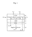
- Fig. 1 shows a conventional light emitting diode structure.
- the conventional LED includes a substrate 10, such as sapphire.
- a buffer layer 12 made of, for example, gallium nitride (GaN) is formed on the substrate 10.
- An n-type GaN layer 14 is formed on the buffer layer 12.
- An active layer such as a multiple quantum well (MQW) layer 16 of AlInGaN, for example, is formed on the n-type GaN layer 14.
- MQW multiple quantum well
- a p-type GaN layer 18 is formed on the MQW layer 16.
- the MQW layer emits photons "h ⁇ " in all directions to illuminate the LED.
- Fig. 1 shows directions 1, 2 and 3 for convenience. Photons traveling in directions 1 and 2 contribute to the intensity of the LED. However, photons traveling in direction 3 become absorbed by the substrate and the package which house the LED. This photon absorption decreases the light extraction efficiency resulting in reduced brightness of the LED.
- the first method is to improve external quantum efficiency of the LED device by epitaxial growth and device structure design.
- This technique requires high quality epitaxial growth techniques that include MOCVD (Metal Organic Chemical Vapor Deposition), MBE (Molecular Beam Epitaxy), and HVPE (Hydride Vapor Phase Epitaxy) and sophisticated device design.
- MOCVD Metal Organic Chemical Vapor Deposition
- MBE Molecular Beam Epitaxy
- HVPE Hydride Vapor Phase Epitaxy
- MOCVD Metal Organic Chemical Vapor Deposition
- MBE Molecular Beam Epitaxy
- HVPE Hydride Vapor Phase Epitaxy
- Another method to enhance the optical light output is increasing the light extraction efficiency by optimizing the LED chip design. Compared to the method of increasing external quantum efficiency by epitaxial growth and device structure design, this method is much simpler and easier to increase the light intensity of the LED device.
- existing designs require high manufacturing cost. Accordingly, a diode is needed that has high brightness capability, an efficient design and low manufacturing cost.
- the present invention is directed to a diode that substantially obviates one or more of the problems due to limitations and disadvantages of the related art.
- An advantage of the present invention is providing a diode having high brightness.
- a light emitting diode comprises a transparent substrate; a buffer layer on a first surface of the transparent substrate; an n-GaN layer on the buffer layer; an active layer on the n-GaN layer; a p-GaN layer on the active layer; a p-electrode on the p-GaN layer; an n-electrode on the n-GaN layer; and a reflective layer on a second side of the transparent substrate.
- a method of making a light emitting diode having a transparent substrate and a buffer layer on a first surface of the transparent substrate comprises forming an n-GaN layer on the buffer layer; forming an active layer on the n-GaN layer; forming a p-GaN layer on the active layer; forming a p-electrode on the p-GaN layer; forming an n-electrode on the n-GaN layer; and forming a reflective layer on a second side of the transparent substrate.
- a method of making a light emitting diode having a transparent substrate and a buffer layer on a first surface of the transparent substrate comprises forming an n-GaN layer on the buffer layer; forming an active layer on the n-GaN layer; forming a p-GaN layer on the active layer; forming a p-electrode on the p-GaN layer; forming an n-electrode on the n-GaN layer; and forming a reflective layer on a second side of the transparent substrate.
- a method of making a light emitting diode having a substrate comprises forming an n-type layer and a p-type layer on the substrate; forming an active layer between the n-type layer and the p-type layer; forming a first electrode contacting the p-type layer; forming a second electrode contacting the n-type layer; and forming a reflective layer on the substrate.
- a diode comprises a transparent substrate; an active layer on the transparent substrate, the active layer generating photons; and a reflective layer on the transparent substrate to reflect the photons from the active layer.
- a method of making a diode comprises forming an active layer over a transparent substrate, the active layer generating photons; and forming a reflective layer on the transparent substrate to reflect the photons from the active layer.
- a method of making a light emitting diode having a transparent substrate comprises forming an n-GaN layer having a first doping concentration on a first side of the transparent substrate; forming an InGaN active layer on the n-GaN layer, the active layer having an In concentration in a first range; forming a p-GaN layer having a second doping concentration on the InGaN active layer; forming a p-type contact layer on the p-GaN layer; forming an n-type contact layer on the n-GaN layer by etching the p-type contact layer, p-GaN layer and the InGaN active layer; reducing a thickness of the transparent substrate by backside lapping at a second surface of the transparent substrate; reducing a surface roughness of the transparent substrate; and forming a reflective layer on a reduced surface of the transparent substrate.
- Fig. 1 generally shows a conventional light emitting diode
- Figs. 2A and 2B show two different embodiments of a light emitting diode of the present invention
- Fig. 3A-3F shows the manufacturing steps for forming the light emitting diode of the present invention
- Figs. 4A and 4B each show a wafer having the light emitting diodes with scribe lines
- Fig. 5 shows another embodiment of the diode of the present invention.
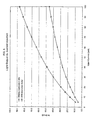
- Fig. 6 is a graph showing a relationship between light output and current injection for an LED having a reflective layer of the present invention and an LED without a reflective layer.
- sapphire substrate In order to fabricate GaN-based light emitting diodes (LEDs), sapphire substrate has been generally used since sapphire is very stable and relatively cheaper.
- the epitaxial layer quality of the AlInGaN grown on sapphire substrate is superior to the other substrate material due to their thermal stability and the same crystal structure of the GaN.
- sapphire there are some disadvantages in using sapphire as a substrate material for AlInGAN-based LED device fabrication. Because the sapphire is insulator, forming an n-type bottom contact is not possible.
- transparent sapphire substrate is beneficial for the light extraction compare to the other non-transparent compound semiconductor material such as GaAs and InP.
- the light output can be increased by making a mirror-like or highly smooth interface between the reflective metal layer and the transparent substrate.
- the reflective index of the substrate material and the surface conditions, including surface roughness there is a certain angle called an escaping angle in which the photons from the active layer reflect off of the interface back to the substrate crystal. Therefore, at a fixed reflective index of the sapphire substrate, for example, the amount of reflected photons can be controlled by reducing the surface roughness of the substrate.
- a new surface polishing technique is employed in addition to the conventional mechanical polishing techniques.
- An atomically flat sapphire surface was obtained using an inductively coupled plasma reactive ion beam etching (ICPRIE).
- the sapphire surface having a surface roughness as small as 1 nm was obtained. Moreover, the transmitted or escaped photons can be reflected back off of the smooth surface to the substrate crystal. This results in a considerable enhancement of the total optical light output of the LED device.
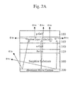
- Fig. 2A illustrates an LED structure of the present invention.
- the light emitting diode structure includes substrate 100, which is a transparent substrate, such as sapphire.
- the sapphire has undergone backside lapping and polishing on its back surface to maximize the light output.
- ICPRIE polishing was performed on a mechanically polished sapphire substrate to further reduce the surface roughness.
- the ICPRIE polishing process conditions were as follows:
- a reflective layer 200 is on the sapphire substrate 100 and can be made of an aluminum mirror, for example, to reflect the photons heading toward the bottom. The reflected photons contribute to dramatically increasing the brightness of the LED.
- the material for the reflective layer is not limited to aluminum but may be any suitable material that will reflect the photons to increase the brightness of the LED.
- the substrate of the LED may also be made of suitable materials other than sapphire.
- Fig. 2B illustrates another LED structure of the present invention.
- the reflective layer is omitted.
- the sapphire substrate 100 is polished using ICPRIE, for example, to maximize the smoothness of the surface of the surface. Such smooth surface allows the photons from the active layer directed toward the sapphire substrate to reflect off from the smooth surface of the sapphire surface to enhance the light output.
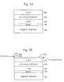
- Figs. 3A-3F illustrate the steps of making a light emitting diode, as an example application of the present invention.
- a buffer layer 120 is formed on a substrate 100.
- the substrate 100 is preferably made from a transparent material including for example, sapphire.
- the substrate can be made of zinc oxide (ZnO), gallium nitride (GaN), silicon carbide (SiC) and aluminum nitride (A1N).
- the buffer layer 120 is made of, for example, GaN (Gallium Nitride) and, in this instance, the GaN was grown on the surface of the sapphire substrate 100.
- An n-type epitaxial layer such as n-GaN 140 is formed on the buffer layer 120.
- the n-GaN layer 140 was doped with silicon (Si) with a doping concentration of about 10 17 cm -3 or greater.
- An active layer 160 such as an AlInGaN multiple quantum well layer is formed on the n-GaN layer 140.
- the active layer 160 may also be formed of a single quantum well layer or a double hetero structure.
- the amount of indium (In) determines whether the diode becomes a green diode or a blue diode.
- indium in the range of about 22% may be used.
- indium in the range of about 40% may be used.
- the amount of indium used may be varied depending on the desired wavelength of the blue or green color.
- a p-GaN layer 180 is formed on the active layer 160.
- the p-GaN layer 180 was doped with magnesium (Mg) with a doping concentration of about 10 17 cm -3 or greater.
- a transparent conductive layer 220 is formed on the p-GaN layer 180.
- the transparent conductive layer 220 may be made of any suitable material including, for example, Ni/Au or indium-tin-oxide (ITO).
- a p-type electrode 240 is then formed on one side of the transparent conductive layer 220.
- the p-type electrode 240 may be made of any suitable material including, for example, Ni/Au, Pd/Au, Pd/Ni and Pt.
- a pad 260 is formed on the p-type electrode 240.
- the pad 260 may be made of any suitable material including, for example, Au.
- the pad 260 may have a thickness of about 5000 ⁇ or higher.
- the transparent conductive layer 220, the p-GaN layer 180, the active layer 160 and the n-GaN layer 140 are all etched at one portion to form an n-electrode 250 and pad 270.
- the n-GaN layer 140 is etched partially so that the n-electrode 250 may be formed on the etched surface of the n-GaN layer 140.
- the n-electrode 250 may be made of any suitable material including, for example, Ti/Al, Cr/Au and Ti/Au.
- the pad 270 is a metal and may be made from the same material as the pad 260.
- the thickness of the substrate 100 is reduced to form a thinner substrate 100A.
- backside lapping is performed on the sapphire substrate 100 to reduce the wafer thickness.
- mechanical polishing is performed to obtain an optically flat surface.
- the surface roughness (Ra) may be less than about 15nm.
- Such polishing technique can reduce the surface roughness up to about 5nm or slightly less. Such low surface roughness adds to the reflective property of the surface.
- the thickness of the substrate 100 can be controlled to be in the range of, for example, 350-430 ⁇ m. Moreover, the thickness can be reduced to less than 350 ⁇ m and to less than 120 ⁇ m.
- mechanical polishing and dry etching techniques are used.
- dry etching inductively coupled plasma (ICP) reactive ion beam etching (RIE) may be used as an example.
- ICP inductively coupled plasma
- RIE reactive ion beam etching
- the surface roughness is further reduced to obtain a surface roughness of less than 1nm.
- the surface roughness can be reduced from 5nm up to less than 1nm by using dry etching.
- dry etching technique is inductively coupled plasma (ICP) reactive ion beam etching (RIE) to obtain an atomically flat surface.
- ICP inductively coupled plasma
- RIE reactive ion beam etching
- the maximum reduction of the surface roughness further enhances the reflectivity of the surface. It is noted that depending on the type of material used for the substrate 100, the surface roughness may be further reduced for maximum reflectivity of the surface.
- a reflective material 200 is formed on the polished thin substrate 100A.
- the reflective material 200 can be any suitable material that can reflect light.
- an aluminum coating of about 300nm thick was formed on the polished sapphire surface 100A using an electron beam evaporation technique.
- the aluminum may have a concentration of about 99.999% or higher, which allows the aluminum to have a mirror-like property with maximum light reflectivity.
- the reflective layer 200 entirely covers the second side of the substrate 100A.
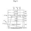
- Fig. 5 shows an alternative embodiment in which a cladding layer 170 is formed between the p-GaN layer 180 and the active layer 160.
- the cladding layer 170 is preferably formed with p-AlGaN.
- the cladding layer 170 enhances the performance of the diode.
- Fig. 5 does not show the p-electrode, n-electrode and the pads.
- the photons generated in the active layer which head toward the polished sapphire surface and the aluminum mirror coating 200 are reflected. Such reflected photons add to the brightness of the diode (photon recovery). Adding the reflective layer and making atomically flat surface greatly increases the brightness of the diode. In addition to the reflective surface of the reflective layer 200, it is important to note that the low surface roughness of the substrate 100 also enhances the photon reflection.
- Fig. 6 is a graph showing a relationship between the light output and the injection current of, for example, a light emitting diode (LED).
- One curve of the graph depicts an LED having a reflective layer (in this case, an aluminum) and the other curve depicts an LED without a reflective layer.
- the reflective aluminum layer was added to the mechanically polished surface of the sapphire substrate, the light output increased about 200% as compared to the device without the reflective layer.
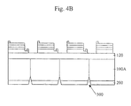
- Fig. 4A shows a wafer having LEDs formed thereon. Scribe lines 300 are formed on the wafer through the buffer layer 120 from the side having the LEDs (front scribing) to separate the LED chips.
- the scribe lines 300 are formed using, for example, a dry etching technique or mechanical scribing.
- the dry etching technique such as inductively coupled plasma (ICP) reactive ion beam etching (RIE) can form very narrow scribe lines on the buffer layer 120 and the substrate 100A.
- ICP inductively coupled plasma
- RIE reactive ion beam etching
- RIE reactive ion beam etching
- the scribe lines may also be formed by a diamond stylus, which requires a large spacing between the diode chips due to the size of the diamond stylus itself. Also, a dicing technique may be used to separate the chips.
- each diode may be packaged. Such package may also be coated with a reflective material to further enhance the light output.
- the present invention applies a simple and inexpensive light extraction process to the existing device fabrication process. According to this invention, adding just one more step of metallization after backside lapping and polishing allows a significant light output increase. With finer polishing using dry etching, in some cases, the light output can be as much as a factor of four without a substantial increase in production cost.
- the diode of the present invention improves light intensity of a diode such as an AlInGaN-based light emitting diode (LED) using a reflective coating.
- the reflective coating recovers those photons, which would otherwise be absorbed by the substrate or the lead frame in the LED package. This increases the total external quantum efficiency of the quantum well devices.
- This invention can be applied not only to the current commercially available blue, green, red and white LEDs but also to other LED devices. Using this technique, the light output was increased by as much as a factor of four as compared to conventional LED devices (without the reflective coating) without significantly sacrificing or changing other characteristics of the diode.
- the reflector and substrate polishing technique of the present invention can easily be applied to other types of diodes including red LEDs and laser diodes including VCSELs.
- red LEDs do not use GaN
- the substrate of the red LEDs may just as easily be polished and a reflective layer can easily be attached to the polished surface of the substrate, as described above.
- Such technique also recovers the photons to increase the light output of the diode. Similar technique is also applicable for laser diodes.
Applications Claiming Priority (2)
| Application Number | Priority Date | Filing Date | Title |
|---|---|---|---|
| US09/982,980 US6949395B2 (en) | 2001-10-22 | 2001-10-22 | Method of making diode having reflective layer |
| EP02793800A EP1459357A4 (de) | 2001-10-22 | 2002-10-21 | Verfahren zur herstellung einer diode mit einer reflektierenden schicht |
Related Parent Applications (1)
| Application Number | Title | Priority Date | Filing Date |
|---|---|---|---|
| EP02793800.0 Division | 2002-10-21 |
Publications (2)
| Publication Number | Publication Date |
|---|---|
| EP2197022A2 true EP2197022A2 (de) | 2010-06-16 |
| EP2197022A3 EP2197022A3 (de) | 2010-09-29 |
Family
ID=25529706
Family Applications (2)
| Application Number | Title | Priority Date | Filing Date |
|---|---|---|---|
| EP02793800A Ceased EP1459357A4 (de) | 2001-10-22 | 2002-10-21 | Verfahren zur herstellung einer diode mit einer reflektierenden schicht |
| EP10158050A Ceased EP2197022A3 (de) | 2001-10-22 | 2002-10-21 | Verfahren zur Herstellung einer Diode mit einer reflektierenden Schicht |
Family Applications Before (1)
| Application Number | Title | Priority Date | Filing Date |
|---|---|---|---|
| EP02793800A Ceased EP1459357A4 (de) | 2001-10-22 | 2002-10-21 | Verfahren zur herstellung einer diode mit einer reflektierenden schicht |
Country Status (5)
| Country | Link |
|---|---|
| US (6) | US6949395B2 (de) |
| EP (2) | EP1459357A4 (de) |
| JP (1) | JP4516749B2 (de) |
| KR (1) | KR100902894B1 (de) |
| WO (1) | WO2003036691A2 (de) |
Families Citing this family (88)
| Publication number | Priority date | Publication date | Assignee | Title |
|---|---|---|---|---|
| JP5283293B2 (ja) * | 2001-02-21 | 2013-09-04 | ソニー株式会社 | 半導体発光素子 |
| US7067849B2 (en) * | 2001-07-17 | 2006-06-27 | Lg Electronics Inc. | Diode having high brightness and method thereof |
| US6949395B2 (en) | 2001-10-22 | 2005-09-27 | Oriol, Inc. | Method of making diode having reflective layer |
| US7148520B2 (en) | 2001-10-26 | 2006-12-12 | Lg Electronics Inc. | Diode having vertical structure and method of manufacturing the same |
| US7279718B2 (en) * | 2002-01-28 | 2007-10-09 | Philips Lumileds Lighting Company, Llc | LED including photonic crystal structure |
| US8294172B2 (en) | 2002-04-09 | 2012-10-23 | Lg Electronics Inc. | Method of fabricating vertical devices using a metal support film |
| TW573372B (en) * | 2002-11-06 | 2004-01-21 | Super Nova Optoelectronics Cor | GaN-based III-V group compound semiconductor light-emitting diode and the manufacturing method thereof |
| US6841802B2 (en) | 2002-06-26 | 2005-01-11 | Oriol, Inc. | Thin film light emitting diode |
| US6831302B2 (en) | 2003-04-15 | 2004-12-14 | Luminus Devices, Inc. | Light emitting devices with improved extraction efficiency |
| KR100593886B1 (ko) * | 2003-06-24 | 2006-07-03 | 삼성전기주식회사 | 질화갈륨계 반도체 발광소자의 제조방법 |
| KR101034055B1 (ko) | 2003-07-18 | 2011-05-12 | 엘지이노텍 주식회사 | 발광 다이오드 및 그 제조방법 |
| US6806112B1 (en) * | 2003-09-22 | 2004-10-19 | National Chung-Hsing University | High brightness light emitting diode |
| JP2005158795A (ja) * | 2003-11-20 | 2005-06-16 | Sumitomo Electric Ind Ltd | 発光ダイオード及び半導体発光装置 |
| KR100576856B1 (ko) * | 2003-12-23 | 2006-05-10 | 삼성전기주식회사 | 질화물 반도체 발광소자 및 제조방법 |
| US7122398B1 (en) * | 2004-03-25 | 2006-10-17 | Nanosolar, Inc. | Manufacturing of optoelectronic devices |
| WO2005104250A1 (en) * | 2004-04-20 | 2005-11-03 | Showa Denko K.K. | Production method of compound semiconductor light-emitting device wafer |
| TWI308397B (en) * | 2004-06-28 | 2009-04-01 | Epistar Corp | Flip-chip light emitting diode and fabricating method thereof |
| US7943949B2 (en) * | 2004-09-09 | 2011-05-17 | Bridgelux, Inc. | III-nitride based on semiconductor device with low-resistance ohmic contacts |
| KR100638666B1 (ko) * | 2005-01-03 | 2006-10-30 | 삼성전기주식회사 | 질화물 반도체 발광소자 |
| TWI250671B (en) * | 2005-03-01 | 2006-03-01 | Epitech Technology Corp | Method for manufacturing light-emitting diode |
| JP2006332257A (ja) * | 2005-05-25 | 2006-12-07 | Sony Corp | ヘテロ接合半導体装置及びその製造方法 |
| KR100667506B1 (ko) * | 2005-08-02 | 2007-01-10 | 엘지전자 주식회사 | 금속 질화막을 갖는 발광 다이오드 및 그 제조방법 |
| TWI256157B (en) * | 2005-09-22 | 2006-06-01 | Epitech Technology Corp | Method for manufacturing light-emitting diode |
| US7547939B2 (en) * | 2005-11-23 | 2009-06-16 | Sensor Electronic Technology, Inc. | Semiconductor device and circuit having multiple voltage controlled capacitors |
| US8729580B2 (en) * | 2005-12-06 | 2014-05-20 | Toshiba Techno Center, Inc. | Light emitter with metal-oxide coating |
| KR100736623B1 (ko) * | 2006-05-08 | 2007-07-09 | 엘지전자 주식회사 | 수직형 발광 소자 및 그 제조방법 |
| KR100735496B1 (ko) * | 2006-05-10 | 2007-07-04 | 삼성전기주식회사 | 수직구조 질화갈륨계 led 소자의 제조방법 |
| KR100784065B1 (ko) * | 2006-09-18 | 2007-12-10 | 엘지이노텍 주식회사 | 질화물 반도체 발광소자 및 그 제조방법 |
| KR101262386B1 (ko) | 2006-09-25 | 2013-05-08 | 엘지이노텍 주식회사 | 질화물 반도체 발광소자의 제조 방법 |
| US20090032799A1 (en) | 2007-06-12 | 2009-02-05 | Siphoton, Inc | Light emitting device |
| US7956370B2 (en) * | 2007-06-12 | 2011-06-07 | Siphoton, Inc. | Silicon based solid state lighting |
| US20100006884A1 (en) * | 2007-08-07 | 2010-01-14 | Epistar Corporation | Light Emitting Device and Manufacturing Method Therof |
| US8153016B2 (en) * | 2007-10-03 | 2012-04-10 | Apple Inc. | Shaping a cover glass |
| JP2009130364A (ja) * | 2007-11-23 | 2009-06-11 | Samsung Electro-Mechanics Co Ltd | 窒化物半導体発光素子及びその製造方法 |
| US7781780B2 (en) * | 2008-03-31 | 2010-08-24 | Bridgelux, Inc. | Light emitting diodes with smooth surface for reflective electrode |
| TWI385826B (zh) * | 2008-05-16 | 2013-02-11 | Epistar Corp | 含漸進式折射率透明基材或具高散熱性質之發光二極體元件及其應用 |
| JP5167974B2 (ja) * | 2008-06-16 | 2013-03-21 | 豊田合成株式会社 | Iii族窒化物系化合物半導体発光素子及びその製造方法 |
| WO2009157921A1 (en) * | 2008-06-24 | 2009-12-30 | Pan Shaoher X | Silicon based solid state lighting |
| US20110114917A1 (en) * | 2008-07-21 | 2011-05-19 | Pan Shaoher X | Light emitting device |
| CN102324454B (zh) * | 2008-09-19 | 2015-01-07 | 晶元光电股份有限公司 | 发光元件及其制造方法 |
| TWI470823B (zh) * | 2009-02-11 | 2015-01-21 | Epistar Corp | 發光元件及其製造方法 |
| KR101072200B1 (ko) * | 2009-03-16 | 2011-10-10 | 엘지이노텍 주식회사 | 발광소자 및 그 제조방법 |
| US8035123B2 (en) * | 2009-03-26 | 2011-10-11 | High Power Opto. Inc. | High light-extraction efficiency light-emitting diode structure |
| US20100308300A1 (en) * | 2009-06-08 | 2010-12-09 | Siphoton, Inc. | Integrated circuit light emission device, module and fabrication process |
| US20120119332A1 (en) * | 2009-06-12 | 2012-05-17 | Petar Branko Atanackovic | Process for producing a semiconductor-on-sapphire article |
| US8963178B2 (en) | 2009-11-13 | 2015-02-24 | Seoul Viosys Co., Ltd. | Light emitting diode chip having distributed bragg reflector and method of fabricating the same |
| TWI531088B (zh) * | 2009-11-13 | 2016-04-21 | 首爾偉傲世有限公司 | 具有分散式布拉格反射器的發光二極體晶片 |
| CN102034912B (zh) * | 2009-12-29 | 2015-03-25 | 比亚迪股份有限公司 | 发光二极管外延片、其制作方法及芯片的制作方法 |
| US8722441B2 (en) | 2010-01-21 | 2014-05-13 | Siphoton Inc. | Manufacturing process for solid state lighting device on a conductive substrate |
| US8674383B2 (en) * | 2010-01-21 | 2014-03-18 | Siphoton Inc. | Solid state lighting device on a conductive substrate |
| US8283676B2 (en) * | 2010-01-21 | 2012-10-09 | Siphoton Inc. | Manufacturing process for solid state lighting device on a conductive substrate |
| KR101159782B1 (ko) * | 2010-02-05 | 2012-06-26 | 신왕균 | 투명 엘이디 웨이퍼 모듈 및 그 제조방법 |
| US8604500B2 (en) | 2010-03-17 | 2013-12-10 | Lg Innotek Co., Ltd. | Light emitting device and light emitting device package |
| KR101047792B1 (ko) | 2010-04-23 | 2011-07-07 | 엘지이노텍 주식회사 | 발광 소자, 발광 소자 제조방법 및 발광 소자 패키지 |
| JP5706962B2 (ja) | 2010-06-24 | 2015-04-22 | ソウル バイオシス カンパニー リミテッドSeoul Viosys Co.,Ltd. | 発光ダイオード |
| US9293678B2 (en) | 2010-07-15 | 2016-03-22 | Micron Technology, Inc. | Solid-state light emitters having substrates with thermal and electrical conductivity enhancements and method of manufacture |
| US8217488B2 (en) * | 2010-07-19 | 2012-07-10 | Walsin Lihwa Corporation | GaN light emitting diode and method for increasing light extraction on GaN light emitting diode via sapphire shaping |
| WO2012015153A2 (en) | 2010-07-28 | 2012-02-02 | Seoul Opto Device Co., Ltd. | Light emitting diode having distributed bragg reflector |
| US8664684B2 (en) * | 2010-08-31 | 2014-03-04 | Micron Technology, Inc. | Solid state lighting devices with improved contacts and associated methods of manufacturing |
| CN102456803A (zh) * | 2010-10-20 | 2012-05-16 | 展晶科技(深圳)有限公司 | 发光二极管封装结构 |
| US8624292B2 (en) | 2011-02-14 | 2014-01-07 | Siphoton Inc. | Non-polar semiconductor light emission devices |
| US8217418B1 (en) | 2011-02-14 | 2012-07-10 | Siphoton Inc. | Semi-polar semiconductor light emission devices |
| US8802545B2 (en) | 2011-03-14 | 2014-08-12 | Plasma-Therm Llc | Method and apparatus for plasma dicing a semi-conductor wafer |
| KR20120126856A (ko) | 2011-05-13 | 2012-11-21 | 삼성전자주식회사 | 반도체 발광다이오드 칩 및 이를 이용한 발광장치 |
| WO2013002503A2 (ko) * | 2011-06-29 | 2013-01-03 | (주)큐엠씨 | 발광 다이오드의 제조 방법 및 장치 |
| US20140183589A1 (en) * | 2011-08-09 | 2014-07-03 | Samsung Electronics Co., Ltd. | Method for manufacturing a semiconductor light-emitting element and semiconductor light-emitting element manufactured thereby |
| CN104040675A (zh) * | 2011-09-29 | 2014-09-10 | 氮化物处理股份有限公司 | 无机材料、制作其的方法和装置、及其使用 |
| JP5724819B2 (ja) * | 2011-10-17 | 2015-05-27 | 日立金属株式会社 | 窒化物半導体成長用基板及びその製造方法、窒化物半導体エピタキシャル基板、並びに窒化物半導体素子 |
| CN102610728B (zh) * | 2012-03-21 | 2014-10-29 | 厦门市三安光电科技有限公司 | 具有背镀反射层的发光二极管及其制作方法 |
| KR20130117474A (ko) * | 2012-04-18 | 2013-10-28 | 서울바이오시스 주식회사 | 배면에 패턴을 갖는 기판을 구비하는 발광다이오드 및 그의 제조방법 |
| US9450152B2 (en) | 2012-05-29 | 2016-09-20 | Micron Technology, Inc. | Solid state transducer dies having reflective features over contacts and associated systems and methods |
| CN102709420B (zh) * | 2012-06-21 | 2014-07-30 | 安徽三安光电有限公司 | 一种氮化镓基发光二极管 |
| WO2014078320A1 (en) * | 2012-11-16 | 2014-05-22 | Electro Scientific Industries, Inc. | Method and apparatus for processing a workpiece and an article formed thereby |
| CN102990229B (zh) * | 2012-11-20 | 2016-04-13 | 大族激光科技产业集团股份有限公司 | 发光二极管晶圆切割方法 |
| US9391241B2 (en) * | 2013-03-15 | 2016-07-12 | Materion Corporation | Light emitting diode |
| JP6175898B2 (ja) * | 2013-05-22 | 2017-08-09 | セイコーエプソン株式会社 | 回折光学素子、回折光学素子の製造方法、及び電子機器 |
| CN104201254B (zh) * | 2014-07-31 | 2018-08-17 | 华灿光电(苏州)有限公司 | 一种具备全角反射镜的发光二极管芯片的制备方法 |
| DE102015109761B4 (de) | 2015-06-18 | 2022-01-27 | OSRAM Opto Semiconductors Gesellschaft mit beschränkter Haftung | Verfahren zur Herstellung eines Nitrid-Halbleiterbauelements und Nitrid-Halbleiterbauelement |
| US9966260B1 (en) | 2015-09-25 | 2018-05-08 | Apple Inc. | Surface modification process for laser application |
| DE102015119553A1 (de) | 2015-11-12 | 2017-05-18 | Osram Opto Semiconductors Gmbh | Strahlungsemittierender Halbleiterchip, optoelektronisches Bauelement mit einem strahlungsemittierenden Halbleiterchip und Verfahren zur Beschichtung eines strahlungsemittierenden Halbleiterchips |
| KR102421964B1 (ko) * | 2016-01-07 | 2022-07-18 | 쑤저우 레킨 세미컨덕터 컴퍼니 리미티드 | 발광 소자 |
| US20170301772A1 (en) * | 2016-04-15 | 2017-10-19 | Robert M. Radway | GaN DEVICES FABRICATED VIA WAFER BONDING |
| CN105976725B (zh) * | 2016-06-20 | 2019-04-02 | 深圳市华星光电技术有限公司 | 微发光二极管显示面板 |
| CN107681034B (zh) * | 2017-08-30 | 2019-11-12 | 天津三安光电有限公司 | 微型发光二极管及其制作方法 |
| DE102018111954B4 (de) * | 2018-05-17 | 2022-02-24 | OSRAM Opto Semiconductors Gesellschaft mit beschränkter Haftung | Verfahren zur herstellung eines halbleiterbauelements mit isolierendem substrat und halbleiterbauelement mit isolierendem substrat und optoelektronische vorrichtung dieses umfassend |
| DE102018116327A1 (de) * | 2018-07-05 | 2020-01-09 | Osram Opto Semiconductors Gmbh | Strahlungsemittierendes Bauteil und Verfahren zur Herstellung eines strahlungsemittierenden Bauteils |
| CN111211038A (zh) * | 2018-11-22 | 2020-05-29 | 东莞新科技术研究开发有限公司 | 晶圆的粗糙处理方法、装置和存储介质 |
| KR20230009413A (ko) * | 2020-07-21 | 2023-01-17 | 엘지전자 주식회사 | 반도체 발광소자 및 반도체 발광소자를 이용한 디스플레이 장치 |
Citations (8)
| Publication number | Priority date | Publication date | Assignee | Title |
|---|---|---|---|---|
| EP0622858A2 (de) * | 1993-04-28 | 1994-11-02 | Nichia Chemical Industries, Ltd. | Halbleitervorrichtung der III-V Verbindung auf Basis einer Galliumnitrid-Halbleiterverbindung und Verfahren zu ihrer Herstellung |
| EP0852816A2 (de) * | 1995-09-29 | 1998-07-15 | Siemens Aktiengesellschaft | Optoelektronisches halbleiter-bauelement |
| US5977566A (en) * | 1996-06-05 | 1999-11-02 | Kabushiki Kaisha Toshiba | Compound semiconductor light emitter |
| EP1017113A1 (de) * | 1997-01-09 | 2000-07-05 | Nichia Chemical Industries, Ltd. | Halbleiteranordnung aus einer nitridverbindung |
| US6097040A (en) * | 1997-07-23 | 2000-08-01 | Sharp Kabushiki Kaisha | Semiconductor light emitting device that prevents current flow in a portion thereof directly under an electrode wire bonding pad |
| US6242761B1 (en) * | 1997-02-21 | 2001-06-05 | Kabushiki Kaisha Toshiba | Nitride compound semiconductor light emitting device |
| JP2001217456A (ja) * | 2000-02-03 | 2001-08-10 | Sharp Corp | 窒化ガリウム系化合物半導体発光素子 |
| US6281524B1 (en) * | 1997-02-21 | 2001-08-28 | Kabushiki Kaisha Toshiba | Semiconductor light-emitting device |
Family Cites Families (129)
| Publication number | Priority date | Publication date | Assignee | Title |
|---|---|---|---|---|
| US41410A (en) * | 1864-01-26 | Improvement in water-elevators | ||
| US37602A (en) * | 1863-02-03 | Improvement in window-sash fastenings | ||
| US117695A (en) * | 1871-08-01 | Improvement in clothes-driers | ||
| US28062A (en) * | 1860-05-01 | Boiler foe preparing paper-stuff | ||
| US30329A (en) * | 1860-10-09 | Abeaugemeijt foe | ||
| US4236296A (en) | 1978-10-13 | 1980-12-02 | Exxon Research & Engineering Co. | Etch method of cleaving semiconductor diode laser wafers |
| US4704369A (en) * | 1985-04-01 | 1987-11-03 | Energy Conversion Devices, Inc. | Method of severing a semiconductor device |
| JP2588280B2 (ja) * | 1989-07-10 | 1997-03-05 | シャープ株式会社 | 化合物半導体発光素子 |
| US5593815A (en) * | 1989-07-31 | 1997-01-14 | Goldstar Co., Ltd. | Cleaving process in manufacturing a semiconductor laser |
| EP0430041B1 (de) * | 1989-11-22 | 1996-02-07 | Daido Tokushuko Kabushiki Kaisha | Lichtemittierende Diode mit lichtreflektierender Schicht |
| US6291257B1 (en) * | 1991-07-21 | 2001-09-18 | Murata Manufacturing Co., Ltd. | Semiconductor photonic device having a ZnO film as a buffer layer and method for forming the ZnO film |
| JP2666228B2 (ja) | 1991-10-30 | 1997-10-22 | 豊田合成株式会社 | 窒化ガリウム系化合物半導体発光素子 |
| US5578839A (en) | 1992-11-20 | 1996-11-26 | Nichia Chemical Industries, Ltd. | Light-emitting gallium nitride-based compound semiconductor device |
| TW230822B (de) * | 1993-03-02 | 1994-09-21 | Sumitomo Electric Industries | |
| JPH07273368A (ja) * | 1994-03-29 | 1995-10-20 | Nec Kansai Ltd | 発光ダイオード |
| US6130147A (en) * | 1994-04-07 | 2000-10-10 | Sdl, Inc. | Methods for forming group III-V arsenide-nitride semiconductor materials |
| US5777350A (en) | 1994-12-02 | 1998-07-07 | Nichia Chemical Industries, Ltd. | Nitride semiconductor light-emitting device |
| US5798537A (en) | 1995-08-31 | 1998-08-25 | Kabushiki Kaisha Toshiba | Blue light-emitting device |
| US6121638A (en) * | 1995-09-12 | 2000-09-19 | Kabushiki Kaisha Toshiba | Multi-layer structured nitride-based semiconductor devices |
| US6017774A (en) * | 1995-12-24 | 2000-01-25 | Sharp Kabushiki Kaisha | Method for producing group III-V compound semiconductor and fabricating light emitting device using such semiconductor |
| US5798536A (en) | 1996-01-25 | 1998-08-25 | Rohm Co., Ltd. | Light-emitting semiconductor device and method for manufacturing the same |
| JPH09307189A (ja) * | 1996-05-14 | 1997-11-28 | Komatsu Ltd | 発光素子および半導体レーザ素子およびこれら素子を用いた装置 |
| RU2152106C1 (ru) * | 1996-06-19 | 2000-06-27 | Матсусита Электрик Индастриал Ко., Лтд. | Оптоэлектронный материал, устройство для его использования и способ изготовления оптоэлектронного материала |
| EP1357584A3 (de) * | 1996-08-01 | 2005-01-12 | Surface Technology Systems Plc | Verfahren zur Oberflachensbehandlung von halbleitenden Substraten |
| JP3636835B2 (ja) * | 1996-08-07 | 2005-04-06 | ローム株式会社 | 基板分割方法およびその基板分割を用いた発光素子製造方法 |
| JP3304787B2 (ja) * | 1996-09-08 | 2002-07-22 | 豊田合成株式会社 | 半導体発光素子及びその製造方法 |
| US6057565A (en) * | 1996-09-26 | 2000-05-02 | Kabushiki Kaisha Toshiba | Semiconductor light emitting device including a non-stoichiometric compound layer and manufacturing method thereof |
| CN1124501C (zh) | 1996-10-30 | 2003-10-15 | 精工爱普生株式会社 | 滤色片及其制造方法 |
| US5904548A (en) * | 1996-11-21 | 1999-05-18 | Texas Instruments Incorporated | Trench scribe line for decreased chip spacing |
| JP3706452B2 (ja) * | 1996-12-24 | 2005-10-12 | ローム株式会社 | 半導体発光素子 |
| US6185238B1 (en) | 1997-02-21 | 2001-02-06 | Kabushiki Kaisha Toshiba | Nitride compound semiconductor laser and its manufacturing method |
| JP3439063B2 (ja) | 1997-03-24 | 2003-08-25 | 三洋電機株式会社 | 半導体発光素子および発光ランプ |
| JP3897186B2 (ja) | 1997-03-27 | 2007-03-22 | シャープ株式会社 | 化合物半導体レーザ |
| JPH10275936A (ja) * | 1997-03-28 | 1998-10-13 | Rohm Co Ltd | 半導体発光素子の製法 |
| JP3769872B2 (ja) * | 1997-05-06 | 2006-04-26 | ソニー株式会社 | 半導体発光素子 |
| US6069021A (en) * | 1997-05-14 | 2000-05-30 | Showa Denko K.K. | Method of growing group III nitride semiconductor crystal layer and semiconductor device incorporating group III nitride semiconductor crystal layer |
| US6239033B1 (en) | 1998-05-28 | 2001-05-29 | Sony Corporation | Manufacturing method of semiconductor device |
| JP3462720B2 (ja) * | 1997-07-16 | 2003-11-05 | 三洋電機株式会社 | n型窒化物半導体の電極及び前記電極を有する半導体素子並びにその製造方法 |
| JPH1168158A (ja) | 1997-08-20 | 1999-03-09 | Sanyo Electric Co Ltd | 窒化ガリウム系化合物半導体装置 |
| JPH11126925A (ja) * | 1997-10-21 | 1999-05-11 | Toyoda Gosei Co Ltd | 窒化ガリウム系化合物半導体発光素子 |
| US5952681A (en) * | 1997-11-24 | 1999-09-14 | Chen; Hsing | Light emitting diode emitting red, green and blue light |
| US6146916A (en) * | 1997-12-02 | 2000-11-14 | Murata Manufacturing Co., Ltd. | Method for forming a GaN-based semiconductor light emitting device |
| JPH11251612A (ja) * | 1998-03-03 | 1999-09-17 | Canon Inc | 光起電力素子の製造方法 |
| US6249534B1 (en) * | 1998-04-06 | 2001-06-19 | Matsushita Electronics Corporation | Nitride semiconductor laser device |
| US6078064A (en) * | 1998-05-04 | 2000-06-20 | Epistar Co. | Indium gallium nitride light emitting diode |
| US6194742B1 (en) | 1998-06-05 | 2001-02-27 | Lumileds Lighting, U.S., Llc | Strain engineered and impurity controlled III-V nitride semiconductor films and optoelectronic devices |
| JP4352473B2 (ja) * | 1998-06-26 | 2009-10-28 | ソニー株式会社 | 半導体装置の製造方法 |
| TW418549B (en) * | 1998-06-26 | 2001-01-11 | Sharp Kk | Crystal growth method for nitride semiconductor, nitride semiconductor light emitting device, and method for producing the same |
| DE19828970C2 (de) * | 1998-06-29 | 2000-05-18 | Siemens Ag | Verfahren zur Herstellung und Vereinzelung von Halbleiter-Lichtemissionsdioden |
| US6504180B1 (en) * | 1998-07-28 | 2003-01-07 | Imec Vzw And Vrije Universiteit | Method of manufacturing surface textured high-efficiency radiating devices and devices obtained therefrom |
| JP3201475B2 (ja) * | 1998-09-14 | 2001-08-20 | 松下電器産業株式会社 | 半導体装置およびその製造方法 |
| KR100277968B1 (ko) * | 1998-09-23 | 2001-03-02 | 구자홍 | 질화갈륨 기판 제조방법 |
| JP4212707B2 (ja) * | 1998-11-26 | 2009-01-21 | スピードファム株式会社 | ウエハ平坦化システム及びウエハ平坦化方法 |
| US6744800B1 (en) * | 1998-12-30 | 2004-06-01 | Xerox Corporation | Method and structure for nitride based laser diode arrays on an insulating substrate |
| KR100316774B1 (ko) * | 1999-01-15 | 2001-12-12 | 이형도 | 마이크로 관성 센서의 제작 방법 |
| US6456638B1 (en) | 1999-02-08 | 2002-09-24 | Fuji Photo Film Co., Ltd. | High-power short-wavelength semiconductor light emitting device having active layer with increased indium content |
| JP2000285409A (ja) * | 1999-03-29 | 2000-10-13 | Toshiba Corp | 磁気ヘッドの製造方法および磁気ヘッド |
| US6375790B1 (en) * | 1999-07-19 | 2002-04-23 | Epion Corporation | Adaptive GCIB for smoothing surfaces |
| JP4412827B2 (ja) * | 1999-08-20 | 2010-02-10 | シャープ株式会社 | 窒化物半導体厚膜基板 |
| JP4282173B2 (ja) * | 1999-09-03 | 2009-06-17 | シャープ株式会社 | 窒素化合物半導体発光素子およびその製造方法 |
| AU7621100A (en) * | 1999-09-29 | 2001-04-30 | Nanovation Technologies, Inc. | Method of forming smooth morphologies in inp-based semiconductors |
| US6492661B1 (en) | 1999-11-04 | 2002-12-10 | Fen-Ren Chien | Light emitting semiconductor device having reflection layer structure |
| JP2001148358A (ja) * | 1999-11-19 | 2001-05-29 | Disco Abrasive Syst Ltd | 半導体ウェーハ及び該半導体ウェーハの分割方法 |
| JP3929008B2 (ja) * | 2000-01-14 | 2007-06-13 | シャープ株式会社 | 窒化物系化合物半導体発光素子およびその製造方法 |
| US6261929B1 (en) * | 2000-02-24 | 2001-07-17 | North Carolina State University | Methods of forming a plurality of semiconductor layers using spaced trench arrays |
| JP4057215B2 (ja) * | 2000-03-07 | 2008-03-05 | 三菱電機株式会社 | 半導体装置の製造方法および液晶表示装置の製造方法 |
| TW497277B (en) | 2000-03-10 | 2002-08-01 | Toshiba Corp | Semiconductor light emitting device and method for manufacturing the same |
| EP1134619A3 (de) | 2000-03-16 | 2003-04-02 | Canon Kabushiki Kaisha | Lichtempfindliches Element, Bildherstellungsapparat und Bildherstellungsverfahren |
| JP3636976B2 (ja) * | 2000-03-17 | 2005-04-06 | 日本電気株式会社 | 窒化物半導体素子およびその製造方法 |
| JP3795298B2 (ja) | 2000-03-31 | 2006-07-12 | 豊田合成株式会社 | Iii族窒化物系化合物半導体発光素子の製造方法 |
| US7319247B2 (en) | 2000-04-26 | 2008-01-15 | Osram Gmbh | Light emitting-diode chip and a method for producing same |
| US6570186B1 (en) * | 2000-05-10 | 2003-05-27 | Toyoda Gosei Co., Ltd. | Light emitting device using group III nitride compound semiconductor |
| TWI289944B (en) | 2000-05-26 | 2007-11-11 | Osram Opto Semiconductors Gmbh | Light-emitting-diode-element with a light-emitting-diode-chip |
| US6693352B1 (en) | 2000-06-05 | 2004-02-17 | Emitronix Inc. | Contact structure for group III-V semiconductor devices and method of producing the same |
| US6562648B1 (en) * | 2000-08-23 | 2003-05-13 | Xerox Corporation | Structure and method for separation and transfer of semiconductor thin films onto dissimilar substrate materials |
| JP4553470B2 (ja) * | 2000-09-13 | 2010-09-29 | 独立行政法人産業技術総合研究所 | p形ZnO系酸化物半導体層の成長方法およびそれを用いた半導体発光素子の製法 |
| JP2002176226A (ja) | 2000-09-22 | 2002-06-21 | Toshiba Corp | 光素子およびその製造方法 |
| US6489250B1 (en) * | 2000-11-21 | 2002-12-03 | United Epitaxy Company Ltd. | Method for cutting group III nitride semiconductor light emitting element |
| US6791119B2 (en) * | 2001-02-01 | 2004-09-14 | Cree, Inc. | Light emitting diodes including modifications for light extraction |
| US6611002B2 (en) * | 2001-02-23 | 2003-08-26 | Nitronex Corporation | Gallium nitride material devices and methods including backside vias |
| US20020117672A1 (en) | 2001-02-23 | 2002-08-29 | Ming-Sung Chu | High-brightness blue-light emitting crystalline structure |
| US6956250B2 (en) * | 2001-02-23 | 2005-10-18 | Nitronex Corporation | Gallium nitride materials including thermally conductive regions |
| US6765232B2 (en) | 2001-03-27 | 2004-07-20 | Ricoh Company, Ltd. | Semiconductor light-emitting device, surface-emission laser diode, and production apparatus thereof, production method, optical module and optical telecommunication system |
| US20020173062A1 (en) * | 2001-05-17 | 2002-11-21 | Lung-Chien Chen | Method for manufacturing GaN-based LED |
| US6479313B1 (en) * | 2001-05-25 | 2002-11-12 | Kopin Corporation | Method of manufacturing GaN-based p-type compound semiconductors and light emitting diodes |
| US6488767B1 (en) * | 2001-06-08 | 2002-12-03 | Advanced Technology Materials, Inc. | High surface quality GaN wafer and method of fabricating same |
| US6787435B2 (en) * | 2001-07-05 | 2004-09-07 | Gelcore Llc | GaN LED with solderable backside metal |
| US7067849B2 (en) * | 2001-07-17 | 2006-06-27 | Lg Electronics Inc. | Diode having high brightness and method thereof |
| US6379985B1 (en) * | 2001-08-01 | 2002-04-30 | Xerox Corporation | Methods for cleaving facets in III-V nitrides grown on c-face sapphire substrates |
| US6734111B2 (en) * | 2001-08-09 | 2004-05-11 | Comlase Ab | Method to GaAs based lasers and a GaAs based laser |
| US6762127B2 (en) * | 2001-08-23 | 2004-07-13 | Yves Pierre Boiteux | Etch process for dielectric materials comprising oxidized organo silane materials |
| US6939735B2 (en) | 2001-09-13 | 2005-09-06 | Tessera Inc. | Microelectronic assembly formation with releasable leads |
| US6526083B1 (en) | 2001-10-09 | 2003-02-25 | Xerox Corporation | Two section blue laser diode with reduced output power droop |
| US6949395B2 (en) | 2001-10-22 | 2005-09-27 | Oriol, Inc. | Method of making diode having reflective layer |
| US7148520B2 (en) | 2001-10-26 | 2006-12-12 | Lg Electronics Inc. | Diode having vertical structure and method of manufacturing the same |
| US6903379B2 (en) * | 2001-11-16 | 2005-06-07 | Gelcore Llc | GaN based LED lighting extraction efficiency using digital diffractive phase grating |
| US6869820B2 (en) | 2002-01-30 | 2005-03-22 | United Epitaxy Co., Ltd. | High efficiency light emitting diode and method of making the same |
| US6819701B2 (en) | 2002-03-26 | 2004-11-16 | Joseph Reid Henrichs | Super-luminescent folded cavity light emitting diode |
| US20030189215A1 (en) | 2002-04-09 | 2003-10-09 | Jong-Lam Lee | Method of fabricating vertical structure leds |
| US8294172B2 (en) | 2002-04-09 | 2012-10-23 | Lg Electronics Inc. | Method of fabricating vertical devices using a metal support film |
| US20040000672A1 (en) | 2002-06-28 | 2004-01-01 | Kopin Corporation | High-power light-emitting diode structures |
| US6841802B2 (en) | 2002-06-26 | 2005-01-11 | Oriol, Inc. | Thin film light emitting diode |
| US6744196B1 (en) | 2002-12-11 | 2004-06-01 | Oriol, Inc. | Thin film LED |
| KR100571816B1 (ko) | 2003-09-08 | 2006-04-17 | 삼성전자주식회사 | 질화물계 발광소자 및 그 제조방법 |
| TW200520266A (en) | 2003-11-21 | 2005-06-16 | Sanken Electric Co Ltd | Semiconductor luminous element and manufacturing method of the same |
| TWI433343B (zh) | 2004-06-22 | 2014-04-01 | Verticle Inc | 具有改良光輸出的垂直構造半導體裝置 |
| WO2006013867A1 (en) | 2004-08-05 | 2006-02-09 | Showa Denko K.K. | Transparent electrode for semiconductor light-emitting device |
| US7291865B2 (en) | 2004-09-29 | 2007-11-06 | Toyoda Gosei Co., Ltd. | Light-emitting semiconductor device |
| WO2006068297A1 (en) * | 2004-12-22 | 2006-06-29 | Matsushita Electric Industrial Co., Ltd. | Semiconductor light emitting device, illumination module, illumination apparatus, method for manufacturing semiconductor light emitting device, and method for manufacturing semiconductor light emitting element |
| US7384808B2 (en) | 2005-07-12 | 2008-06-10 | Visual Photonics Epitaxy Co., Ltd. | Fabrication method of high-brightness light emitting diode having reflective layer |
| US7875474B2 (en) | 2005-09-06 | 2011-01-25 | Show A Denko K.K. | Gallium nitride-based compound semiconductor light-emitting device and production method thereof |
| JP2007087973A (ja) | 2005-09-16 | 2007-04-05 | Rohm Co Ltd | 窒化物半導体素子の製法およびその方法により得られる窒化物半導体発光素子 |
| JP4137936B2 (ja) | 2005-11-16 | 2008-08-20 | 昭和電工株式会社 | 窒化ガリウム系化合物半導体発光素子 |
| KR101261214B1 (ko) * | 2006-05-18 | 2013-05-06 | 서울옵토디바이스주식회사 | 발광 다이오드 제조방법 |
| JP4854566B2 (ja) | 2006-06-15 | 2012-01-18 | シャープ株式会社 | 窒化物半導体発光素子の製造方法および窒化物半導体発光素子 |
| KR101262386B1 (ko) * | 2006-09-25 | 2013-05-08 | 엘지이노텍 주식회사 | 질화물 반도체 발광소자의 제조 방법 |
| JP2008117824A (ja) | 2006-11-01 | 2008-05-22 | Sharp Corp | 窒化物系半導体素子の製造方法 |
| JP2008182110A (ja) | 2007-01-25 | 2008-08-07 | Matsushita Electric Ind Co Ltd | 窒化物半導体発光装置 |
| US9634191B2 (en) | 2007-11-14 | 2017-04-25 | Cree, Inc. | Wire bond free wafer level LED |
| JP2009283912A (ja) * | 2008-04-25 | 2009-12-03 | Sanyo Electric Co Ltd | 窒化物系半導体素子およびその製造方法 |
| TWI464899B (zh) * | 2008-05-09 | 2014-12-11 | Advanced Optoelectronic Tech | A method for manufacturing a semiconductor element |
| JP2010003768A (ja) | 2008-06-18 | 2010-01-07 | Showa Denko Kk | Iii族窒化物半導体発光素子及びその製造方法、並びにランプ |
| JP2010205988A (ja) * | 2009-03-04 | 2010-09-16 | Panasonic Corp | 窒化物半導体素子及びその製造方法 |
| JP5517882B2 (ja) * | 2010-10-20 | 2014-06-11 | シャープ株式会社 | 窒化物半導体発光素子 |
| US20130146928A1 (en) * | 2011-04-06 | 2013-06-13 | Panasonic Corporation | Semiconductor light-emitting device |
| JP5729335B2 (ja) * | 2012-03-19 | 2015-06-03 | 豊田合成株式会社 | Iii族窒化物半導体発光素子およびその製造方法 |
| WO2013148955A1 (en) * | 2012-03-28 | 2013-10-03 | Sensor Electronic Technology, Inc. | Light emitting device substrate with inclined sidewalls |
| TWI488336B (zh) * | 2012-06-07 | 2015-06-11 | Lextar Electronics Corp | 發光二極體及其製造方法 |
| KR102087933B1 (ko) * | 2012-11-05 | 2020-04-14 | 엘지이노텍 주식회사 | 발광 소자 및 이를 포함하는 발광 소자 어레이 |
-
2001
- 2001-10-22 US US09/982,980 patent/US6949395B2/en not_active Expired - Lifetime
-
2002
- 2002-10-21 WO PCT/US2002/033357 patent/WO2003036691A2/en active Application Filing
- 2002-10-21 EP EP02793800A patent/EP1459357A4/de not_active Ceased
- 2002-10-21 KR KR1020047005880A patent/KR100902894B1/ko active IP Right Grant
- 2002-10-21 JP JP2003539082A patent/JP4516749B2/ja not_active Expired - Fee Related
- 2002-10-21 EP EP10158050A patent/EP2197022A3/de not_active Ceased
-
2005
- 2005-08-15 US US11/203,322 patent/US7682854B2/en not_active Expired - Lifetime
-
2007
- 2007-03-02 US US11/713,045 patent/US7785908B2/en not_active Expired - Lifetime
-
2010
- 2010-07-22 US US12/841,674 patent/US8236585B2/en not_active Expired - Lifetime
-
2012
- 2012-07-16 US US13/550,097 patent/US8759129B2/en not_active Expired - Fee Related
-
2014
- 2014-06-03 US US14/294,732 patent/US9406837B2/en not_active Expired - Lifetime
Patent Citations (8)
| Publication number | Priority date | Publication date | Assignee | Title |
|---|---|---|---|---|
| EP0622858A2 (de) * | 1993-04-28 | 1994-11-02 | Nichia Chemical Industries, Ltd. | Halbleitervorrichtung der III-V Verbindung auf Basis einer Galliumnitrid-Halbleiterverbindung und Verfahren zu ihrer Herstellung |
| EP0852816A2 (de) * | 1995-09-29 | 1998-07-15 | Siemens Aktiengesellschaft | Optoelektronisches halbleiter-bauelement |
| US5977566A (en) * | 1996-06-05 | 1999-11-02 | Kabushiki Kaisha Toshiba | Compound semiconductor light emitter |
| EP1017113A1 (de) * | 1997-01-09 | 2000-07-05 | Nichia Chemical Industries, Ltd. | Halbleiteranordnung aus einer nitridverbindung |
| US6242761B1 (en) * | 1997-02-21 | 2001-06-05 | Kabushiki Kaisha Toshiba | Nitride compound semiconductor light emitting device |
| US6281524B1 (en) * | 1997-02-21 | 2001-08-28 | Kabushiki Kaisha Toshiba | Semiconductor light-emitting device |
| US6097040A (en) * | 1997-07-23 | 2000-08-01 | Sharp Kabushiki Kaisha | Semiconductor light emitting device that prevents current flow in a portion thereof directly under an electrode wire bonding pad |
| JP2001217456A (ja) * | 2000-02-03 | 2001-08-10 | Sharp Corp | 窒化ガリウム系化合物半導体発光素子 |
Also Published As
| Publication number | Publication date |
|---|---|
| JP4516749B2 (ja) | 2010-08-04 |
| US20060006400A1 (en) | 2006-01-12 |
| EP2197022A3 (de) | 2010-09-29 |
| US6949395B2 (en) | 2005-09-27 |
| US20140273322A1 (en) | 2014-09-18 |
| US9406837B2 (en) | 2016-08-02 |
| WO2003036691A3 (en) | 2003-06-05 |
| EP1459357A2 (de) | 2004-09-22 |
| KR20040063128A (ko) | 2004-07-12 |
| EP1459357A4 (de) | 2006-10-25 |
| WO2003036691A2 (en) | 2003-05-01 |
| US7785908B2 (en) | 2010-08-31 |
| US8759129B2 (en) | 2014-06-24 |
| US20030077847A1 (en) | 2003-04-24 |
| US20100285621A1 (en) | 2010-11-11 |
| US20120322176A1 (en) | 2012-12-20 |
| JP2006507654A (ja) | 2006-03-02 |
| KR100902894B1 (ko) | 2009-06-16 |
| US8236585B2 (en) | 2012-08-07 |
| US7682854B2 (en) | 2010-03-23 |
| US20070172973A1 (en) | 2007-07-26 |
Similar Documents
| Publication | Publication Date | Title |
|---|---|---|
| US10553744B2 (en) | Diode having high brightness and method thereof | |
| US9406837B2 (en) | Method of making diode having reflective layer | |
| US10032959B2 (en) | Diode having vertical structure |
Legal Events
| Date | Code | Title | Description |
|---|---|---|---|
| PUAI | Public reference made under article 153(3) epc to a published international application that has entered the european phase |
Free format text: ORIGINAL CODE: 0009012 |
|
| 17P | Request for examination filed |
Effective date: 20100326 |
|
| AC | Divisional application: reference to earlier application |
Ref document number: 1459357 Country of ref document: EP Kind code of ref document: P |
|
| AK | Designated contracting states |
Kind code of ref document: A2 Designated state(s): AT BE BG CH CY CZ DE DK EE ES FI FR GB GR IE IT LI LU MC NL PT SE SK TR |
|
| AX | Request for extension of the european patent |
Extension state: AL LT LV MK RO SI |
|
| PUAL | Search report despatched |
Free format text: ORIGINAL CODE: 0009013 |
|
| AK | Designated contracting states |
Kind code of ref document: A3 Designated state(s): AT BE BG CH CY CZ DE DK EE ES FI FR GB GR IE IT LI LU MC NL PT SE SK TR |
|
| AX | Request for extension of the european patent |
Extension state: AL LT LV MK RO SI |
|
| 17Q | First examination report despatched |
Effective date: 20111221 |
|
| RAP1 | Party data changed (applicant data changed or rights of an application transferred) |
Owner name: LG INNOTEK CO., LTD. |
|
| STAA | Information on the status of an ep patent application or granted ep patent |
Free format text: STATUS: THE APPLICATION HAS BEEN REFUSED |
|
| 18R | Application refused |
Effective date: 20141208 |