EP0622858A2 - Halbleitervorrichtung der III-V Verbindung auf Basis einer Galliumnitrid-Halbleiterverbindung und Verfahren zu ihrer Herstellung - Google Patents
Halbleitervorrichtung der III-V Verbindung auf Basis einer Galliumnitrid-Halbleiterverbindung und Verfahren zu ihrer Herstellung Download PDFInfo
- Publication number
- EP0622858A2 EP0622858A2 EP94106587A EP94106587A EP0622858A2 EP 0622858 A2 EP0622858 A2 EP 0622858A2 EP 94106587 A EP94106587 A EP 94106587A EP 94106587 A EP94106587 A EP 94106587A EP 0622858 A2 EP0622858 A2 EP 0622858A2
- Authority
- EP
- European Patent Office
- Prior art keywords
- layer
- electrode
- semiconductor layer
- gold
- titanium
- Prior art date
- Legal status (The legal status is an assumption and is not a legal conclusion. Google has not performed a legal analysis and makes no representation as to the accuracy of the status listed.)
- Granted
Links
- 239000004065 semiconductor Substances 0.000 title claims abstract description 213
- 229910002601 GaN Inorganic materials 0.000 title claims abstract description 115
- 150000001875 compounds Chemical class 0.000 title claims abstract description 98
- JMASRVWKEDWRBT-UHFFFAOYSA-N Gallium nitride Chemical compound [Ga]#N JMASRVWKEDWRBT-UHFFFAOYSA-N 0.000 title claims abstract description 83
- 238000000034 method Methods 0.000 title claims description 23
- 239000007769 metal material Substances 0.000 claims abstract description 88
- 239000000758 substrate Substances 0.000 claims abstract description 47
- PCHJSUWPFVWCPO-UHFFFAOYSA-N gold Chemical compound [Au] PCHJSUWPFVWCPO-UHFFFAOYSA-N 0.000 claims description 114
- 239000010931 gold Substances 0.000 claims description 109
- 229910052737 gold Inorganic materials 0.000 claims description 104
- PXHVJJICTQNCMI-UHFFFAOYSA-N Nickel Chemical compound [Ni] PXHVJJICTQNCMI-UHFFFAOYSA-N 0.000 claims description 92
- 239000010936 titanium Substances 0.000 claims description 82
- RTAQQCXQSZGOHL-UHFFFAOYSA-N Titanium Chemical compound [Ti] RTAQQCXQSZGOHL-UHFFFAOYSA-N 0.000 claims description 81
- 229910052719 titanium Inorganic materials 0.000 claims description 80
- 229910052782 aluminium Inorganic materials 0.000 claims description 79
- XAGFODPZIPBFFR-UHFFFAOYSA-N aluminium Chemical compound [Al] XAGFODPZIPBFFR-UHFFFAOYSA-N 0.000 claims description 75
- 238000000137 annealing Methods 0.000 claims description 52
- 229910052759 nickel Inorganic materials 0.000 claims description 46
- 229910052751 metal Inorganic materials 0.000 claims description 35
- 239000002184 metal Substances 0.000 claims description 35
- 230000001681 protective effect Effects 0.000 claims description 25
- BASFCYQUMIYNBI-UHFFFAOYSA-N platinum Chemical compound [Pt] BASFCYQUMIYNBI-UHFFFAOYSA-N 0.000 claims description 24
- 150000002739 metals Chemical class 0.000 claims description 20
- 229910052804 chromium Inorganic materials 0.000 claims description 19
- 239000011651 chromium Substances 0.000 claims description 19
- VYZAMTAEIAYCRO-UHFFFAOYSA-N Chromium Chemical compound [Cr] VYZAMTAEIAYCRO-UHFFFAOYSA-N 0.000 claims description 18
- 239000000463 material Substances 0.000 claims description 17
- 229910052738 indium Inorganic materials 0.000 claims description 15
- APFVFJFRJDLVQX-UHFFFAOYSA-N indium atom Chemical compound [In] APFVFJFRJDLVQX-UHFFFAOYSA-N 0.000 claims description 15
- 238000002844 melting Methods 0.000 claims description 12
- 229910052697 platinum Inorganic materials 0.000 claims description 12
- ATJFFYVFTNAWJD-UHFFFAOYSA-N Tin Chemical compound [Sn] ATJFFYVFTNAWJD-UHFFFAOYSA-N 0.000 claims description 4
- 229910052718 tin Inorganic materials 0.000 claims description 4
- 229910052581 Si3N4 Inorganic materials 0.000 claims description 3
- VYPSYNLAJGMNEJ-UHFFFAOYSA-N Silicium dioxide Chemical compound O=[Si]=O VYPSYNLAJGMNEJ-UHFFFAOYSA-N 0.000 claims description 3
- GWEVSGVZZGPLCZ-UHFFFAOYSA-N Titan oxide Chemical compound O=[Ti]=O GWEVSGVZZGPLCZ-UHFFFAOYSA-N 0.000 claims description 3
- TWNQGVIAIRXVLR-UHFFFAOYSA-N oxo(oxoalumanyloxy)alumane Chemical compound O=[Al]O[Al]=O TWNQGVIAIRXVLR-UHFFFAOYSA-N 0.000 claims description 3
- HQVNEWCFYHHQES-UHFFFAOYSA-N silicon nitride Chemical compound N12[Si]34N5[Si]62N3[Si]51N64 HQVNEWCFYHHQES-UHFFFAOYSA-N 0.000 claims description 3
- 229910052814 silicon oxide Inorganic materials 0.000 claims description 3
- OGIDPMRJRNCKJF-UHFFFAOYSA-N titanium oxide Inorganic materials [Ti]=O OGIDPMRJRNCKJF-UHFFFAOYSA-N 0.000 claims description 3
- 230000008018 melting Effects 0.000 claims description 2
- 238000002474 experimental method Methods 0.000 description 24
- 239000010408 film Substances 0.000 description 23
- 239000007772 electrode material Substances 0.000 description 22
- 239000002019 doping agent Substances 0.000 description 16
- 238000000151 deposition Methods 0.000 description 13
- XUIMIQQOPSSXEZ-UHFFFAOYSA-N Silicon Chemical compound [Si] XUIMIQQOPSSXEZ-UHFFFAOYSA-N 0.000 description 12
- 229910052710 silicon Inorganic materials 0.000 description 12
- 239000010703 silicon Substances 0.000 description 12
- IJGRMHOSHXDMSA-UHFFFAOYSA-N Atomic nitrogen Chemical compound N#N IJGRMHOSHXDMSA-UHFFFAOYSA-N 0.000 description 10
- 229910052594 sapphire Inorganic materials 0.000 description 10
- 239000010980 sapphire Substances 0.000 description 10
- 239000010409 thin film Substances 0.000 description 10
- 229910045601 alloy Inorganic materials 0.000 description 7
- 239000000956 alloy Substances 0.000 description 7
- 239000011777 magnesium Substances 0.000 description 7
- FYYHWMGAXLPEAU-UHFFFAOYSA-N Magnesium Chemical compound [Mg] FYYHWMGAXLPEAU-UHFFFAOYSA-N 0.000 description 6
- 230000007423 decrease Effects 0.000 description 6
- 229910052749 magnesium Inorganic materials 0.000 description 6
- 239000000853 adhesive Substances 0.000 description 5
- 230000001070 adhesive effect Effects 0.000 description 5
- 230000000052 comparative effect Effects 0.000 description 5
- 238000005259 measurement Methods 0.000 description 5
- 229910052757 nitrogen Inorganic materials 0.000 description 5
- 125000004435 hydrogen atom Chemical group [H]* 0.000 description 4
- 238000012986 modification Methods 0.000 description 4
- 230000004048 modification Effects 0.000 description 4
- UFHFLCQGNIYNRP-UHFFFAOYSA-N Hydrogen Chemical compound [H][H] UFHFLCQGNIYNRP-UHFFFAOYSA-N 0.000 description 3
- 229910004349 Ti-Al Inorganic materials 0.000 description 3
- 229910004692 Ti—Al Inorganic materials 0.000 description 3
- 230000003064 anti-oxidating effect Effects 0.000 description 3
- 239000013078 crystal Substances 0.000 description 3
- 230000000694 effects Effects 0.000 description 3
- 239000011669 selenium Substances 0.000 description 3
- 229910018170 Al—Au Inorganic materials 0.000 description 2
- 229910018575 Al—Ti Inorganic materials 0.000 description 2
- QGZKDVFQNNGYKY-UHFFFAOYSA-N Ammonia Chemical compound N QGZKDVFQNNGYKY-UHFFFAOYSA-N 0.000 description 2
- 229910001020 Au alloy Inorganic materials 0.000 description 2
- -1 GaN Chemical compound 0.000 description 2
- GYHNNYVSQQEPJS-UHFFFAOYSA-N Gallium Chemical compound [Ga] GYHNNYVSQQEPJS-UHFFFAOYSA-N 0.000 description 2
- OAKJQQAXSVQMHS-UHFFFAOYSA-N Hydrazine Chemical compound NN OAKJQQAXSVQMHS-UHFFFAOYSA-N 0.000 description 2
- BUGBHKTXTAQXES-UHFFFAOYSA-N Selenium Chemical compound [Se] BUGBHKTXTAQXES-UHFFFAOYSA-N 0.000 description 2
- NINIDFKCEFEMDL-UHFFFAOYSA-N Sulfur Chemical compound [S] NINIDFKCEFEMDL-UHFFFAOYSA-N 0.000 description 2
- 229910001069 Ti alloy Inorganic materials 0.000 description 2
- HCHKCACWOHOZIP-UHFFFAOYSA-N Zinc Chemical compound [Zn] HCHKCACWOHOZIP-UHFFFAOYSA-N 0.000 description 2
- 239000012298 atmosphere Substances 0.000 description 2
- 238000005229 chemical vapour deposition Methods 0.000 description 2
- 238000000354 decomposition reaction Methods 0.000 description 2
- 238000005530 etching Methods 0.000 description 2
- 229910052733 gallium Inorganic materials 0.000 description 2
- 229910052732 germanium Inorganic materials 0.000 description 2
- GNPVGFCGXDBREM-UHFFFAOYSA-N germanium atom Chemical compound [Ge] GNPVGFCGXDBREM-UHFFFAOYSA-N 0.000 description 2
- 229910052739 hydrogen Inorganic materials 0.000 description 2
- 239000001257 hydrogen Substances 0.000 description 2
- 239000012535 impurity Substances 0.000 description 2
- 238000004519 manufacturing process Methods 0.000 description 2
- 238000002488 metal-organic chemical vapour deposition Methods 0.000 description 2
- 239000000203 mixture Substances 0.000 description 2
- 230000003647 oxidation Effects 0.000 description 2
- 238000007254 oxidation reaction Methods 0.000 description 2
- 230000001590 oxidative effect Effects 0.000 description 2
- 238000009877 rendering Methods 0.000 description 2
- 229910052711 selenium Inorganic materials 0.000 description 2
- 238000004544 sputter deposition Methods 0.000 description 2
- 239000011593 sulfur Substances 0.000 description 2
- 229910052717 sulfur Inorganic materials 0.000 description 2
- 238000007740 vapor deposition Methods 0.000 description 2
- 238000001947 vapour-phase growth Methods 0.000 description 2
- 239000011701 zinc Substances 0.000 description 2
- 229910052725 zinc Inorganic materials 0.000 description 2
- JBRZTFJDHDCESZ-UHFFFAOYSA-N AsGa Chemical compound [As]#[Ga] JBRZTFJDHDCESZ-UHFFFAOYSA-N 0.000 description 1
- RYGMFSIKBFXOCR-UHFFFAOYSA-N Copper Chemical compound [Cu] RYGMFSIKBFXOCR-UHFFFAOYSA-N 0.000 description 1
- 108091006149 Electron carriers Proteins 0.000 description 1
- ZOKXTWBITQBERF-UHFFFAOYSA-N Molybdenum Chemical compound [Mo] ZOKXTWBITQBERF-UHFFFAOYSA-N 0.000 description 1
- XLOMVQKBTHCTTD-UHFFFAOYSA-N Zinc monoxide Chemical compound [Zn]=O XLOMVQKBTHCTTD-UHFFFAOYSA-N 0.000 description 1
- 238000005275 alloying Methods 0.000 description 1
- 229910021529 ammonia Inorganic materials 0.000 description 1
- 229910052788 barium Inorganic materials 0.000 description 1
- DSAJWYNOEDNPEQ-UHFFFAOYSA-N barium atom Chemical compound [Ba] DSAJWYNOEDNPEQ-UHFFFAOYSA-N 0.000 description 1
- 230000004888 barrier function Effects 0.000 description 1
- 229910052790 beryllium Inorganic materials 0.000 description 1
- ATBAMAFKBVZNFJ-UHFFFAOYSA-N beryllium atom Chemical compound [Be] ATBAMAFKBVZNFJ-UHFFFAOYSA-N 0.000 description 1
- 229910052799 carbon Inorganic materials 0.000 description 1
- 239000012159 carrier gas Substances 0.000 description 1
- 238000007796 conventional method Methods 0.000 description 1
- 229910052802 copper Inorganic materials 0.000 description 1
- 239000010949 copper Substances 0.000 description 1
- 230000000593 degrading effect Effects 0.000 description 1
- 230000002708 enhancing effect Effects 0.000 description 1
- HZXMRANICFIONG-UHFFFAOYSA-N gallium phosphide Chemical compound [Ga]#P HZXMRANICFIONG-UHFFFAOYSA-N 0.000 description 1
- 239000003353 gold alloy Substances 0.000 description 1
- 150000004678 hydrides Chemical class 0.000 description 1
- 230000006872 improvement Effects 0.000 description 1
- 238000001451 molecular beam epitaxy Methods 0.000 description 1
- 229910052750 molybdenum Inorganic materials 0.000 description 1
- 239000011733 molybdenum Substances 0.000 description 1
- 150000004767 nitrides Chemical class 0.000 description 1
- 239000012299 nitrogen atmosphere Substances 0.000 description 1
- 230000035945 sensitivity Effects 0.000 description 1
- HBMJWWWQQXIZIP-UHFFFAOYSA-N silicon carbide Chemical compound [Si+]#[C-] HBMJWWWQQXIZIP-UHFFFAOYSA-N 0.000 description 1
- 229910000679 solder Inorganic materials 0.000 description 1
- 229910052712 strontium Inorganic materials 0.000 description 1
- CIOAGBVUUVVLOB-UHFFFAOYSA-N strontium atom Chemical compound [Sr] CIOAGBVUUVVLOB-UHFFFAOYSA-N 0.000 description 1
- 238000010301 surface-oxidation reaction Methods 0.000 description 1
- JBQYATWDVHIOAR-UHFFFAOYSA-N tellanylidenegermanium Chemical compound [Te]=[Ge] JBQYATWDVHIOAR-UHFFFAOYSA-N 0.000 description 1
- 229910052714 tellurium Inorganic materials 0.000 description 1
- PORWMNRCUJJQNO-UHFFFAOYSA-N tellurium atom Chemical compound [Te] PORWMNRCUJJQNO-UHFFFAOYSA-N 0.000 description 1
- 238000012360 testing method Methods 0.000 description 1
- 238000005979 thermal decomposition reaction Methods 0.000 description 1
- XCZXGTMEAKBVPV-UHFFFAOYSA-N trimethylgallium Chemical compound C[Ga](C)C XCZXGTMEAKBVPV-UHFFFAOYSA-N 0.000 description 1
- WFKWXMTUELFFGS-UHFFFAOYSA-N tungsten Chemical compound [W] WFKWXMTUELFFGS-UHFFFAOYSA-N 0.000 description 1
- 229910052721 tungsten Inorganic materials 0.000 description 1
- 239000010937 tungsten Substances 0.000 description 1
Images


Classifications
-
- H—ELECTRICITY
- H01—ELECTRIC ELEMENTS
- H01L—SEMICONDUCTOR DEVICES NOT COVERED BY CLASS H10
- H01L33/00—Semiconductor devices with at least one potential-jump barrier or surface barrier specially adapted for light emission; Processes or apparatus specially adapted for the manufacture or treatment thereof or of parts thereof; Details thereof
- H01L33/36—Semiconductor devices with at least one potential-jump barrier or surface barrier specially adapted for light emission; Processes or apparatus specially adapted for the manufacture or treatment thereof or of parts thereof; Details thereof characterised by the electrodes
- H01L33/40—Materials therefor
-
- H—ELECTRICITY
- H01—ELECTRIC ELEMENTS
- H01L—SEMICONDUCTOR DEVICES NOT COVERED BY CLASS H10
- H01L21/00—Processes or apparatus adapted for the manufacture or treatment of semiconductor or solid state devices or of parts thereof
- H01L21/02—Manufacture or treatment of semiconductor devices or of parts thereof
- H01L21/04—Manufacture or treatment of semiconductor devices or of parts thereof the devices having at least one potential-jump barrier or surface barrier, e.g. PN junction, depletion layer or carrier concentration layer
- H01L21/18—Manufacture or treatment of semiconductor devices or of parts thereof the devices having at least one potential-jump barrier or surface barrier, e.g. PN junction, depletion layer or carrier concentration layer the devices having semiconductor bodies comprising elements of Group IV of the Periodic System or AIIIBV compounds with or without impurities, e.g. doping materials
- H01L21/28—Manufacture of electrodes on semiconductor bodies using processes or apparatus not provided for in groups H01L21/20 - H01L21/268
- H01L21/283—Deposition of conductive or insulating materials for electrodes conducting electric current
- H01L21/285—Deposition of conductive or insulating materials for electrodes conducting electric current from a gas or vapour, e.g. condensation
- H01L21/28506—Deposition of conductive or insulating materials for electrodes conducting electric current from a gas or vapour, e.g. condensation of conductive layers
- H01L21/28575—Deposition of conductive or insulating materials for electrodes conducting electric current from a gas or vapour, e.g. condensation of conductive layers on semiconductor bodies comprising AIIIBV compounds
-
- H—ELECTRICITY
- H01—ELECTRIC ELEMENTS
- H01L—SEMICONDUCTOR DEVICES NOT COVERED BY CLASS H10
- H01L31/00—Semiconductor devices sensitive to infrared radiation, light, electromagnetic radiation of shorter wavelength or corpuscular radiation and specially adapted either for the conversion of the energy of such radiation into electrical energy or for the control of electrical energy by such radiation; Processes or apparatus specially adapted for the manufacture or treatment thereof or of parts thereof; Details thereof
- H01L31/18—Processes or apparatus specially adapted for the manufacture or treatment of these devices or of parts thereof
- H01L31/1884—Manufacture of transparent electrodes, e.g. TCO, ITO
-
- H—ELECTRICITY
- H01—ELECTRIC ELEMENTS
- H01L—SEMICONDUCTOR DEVICES NOT COVERED BY CLASS H10
- H01L33/00—Semiconductor devices with at least one potential-jump barrier or surface barrier specially adapted for light emission; Processes or apparatus specially adapted for the manufacture or treatment thereof or of parts thereof; Details thereof
- H01L33/02—Semiconductor devices with at least one potential-jump barrier or surface barrier specially adapted for light emission; Processes or apparatus specially adapted for the manufacture or treatment thereof or of parts thereof; Details thereof characterised by the semiconductor bodies
- H01L33/26—Materials of the light emitting region
- H01L33/30—Materials of the light emitting region containing only elements of group III and group V of the periodic system
- H01L33/32—Materials of the light emitting region containing only elements of group III and group V of the periodic system containing nitrogen
- H01L33/325—Materials of the light emitting region containing only elements of group III and group V of the periodic system containing nitrogen characterised by the doping materials
-
- H—ELECTRICITY
- H01—ELECTRIC ELEMENTS
- H01L—SEMICONDUCTOR DEVICES NOT COVERED BY CLASS H10
- H01L33/00—Semiconductor devices with at least one potential-jump barrier or surface barrier specially adapted for light emission; Processes or apparatus specially adapted for the manufacture or treatment thereof or of parts thereof; Details thereof
- H01L33/36—Semiconductor devices with at least one potential-jump barrier or surface barrier specially adapted for light emission; Processes or apparatus specially adapted for the manufacture or treatment thereof or of parts thereof; Details thereof characterised by the electrodes
- H01L33/40—Materials therefor
- H01L33/42—Transparent materials
-
- H—ELECTRICITY
- H01—ELECTRIC ELEMENTS
- H01L—SEMICONDUCTOR DEVICES NOT COVERED BY CLASS H10
- H01L2224/00—Indexing scheme for arrangements for connecting or disconnecting semiconductor or solid-state bodies and methods related thereto as covered by H01L24/00
- H01L2224/01—Means for bonding being attached to, or being formed on, the surface to be connected, e.g. chip-to-package, die-attach, "first-level" interconnects; Manufacturing methods related thereto
- H01L2224/02—Bonding areas; Manufacturing methods related thereto
- H01L2224/04—Structure, shape, material or disposition of the bonding areas prior to the connecting process
- H01L2224/04042—Bonding areas specifically adapted for wire connectors, e.g. wirebond pads
-
- H—ELECTRICITY
- H01—ELECTRIC ELEMENTS
- H01L—SEMICONDUCTOR DEVICES NOT COVERED BY CLASS H10
- H01L2224/00—Indexing scheme for arrangements for connecting or disconnecting semiconductor or solid-state bodies and methods related thereto as covered by H01L24/00
- H01L2224/01—Means for bonding being attached to, or being formed on, the surface to be connected, e.g. chip-to-package, die-attach, "first-level" interconnects; Manufacturing methods related thereto
- H01L2224/02—Bonding areas; Manufacturing methods related thereto
- H01L2224/04—Structure, shape, material or disposition of the bonding areas prior to the connecting process
- H01L2224/05—Structure, shape, material or disposition of the bonding areas prior to the connecting process of an individual bonding area
- H01L2224/05001—Internal layers
- H01L2224/05075—Plural internal layers
- H01L2224/0508—Plural internal layers being stacked
- H01L2224/05082—Two-layer arrangements
-
- H—ELECTRICITY
- H01—ELECTRIC ELEMENTS
- H01L—SEMICONDUCTOR DEVICES NOT COVERED BY CLASS H10
- H01L2224/00—Indexing scheme for arrangements for connecting or disconnecting semiconductor or solid-state bodies and methods related thereto as covered by H01L24/00
- H01L2224/01—Means for bonding being attached to, or being formed on, the surface to be connected, e.g. chip-to-package, die-attach, "first-level" interconnects; Manufacturing methods related thereto
- H01L2224/02—Bonding areas; Manufacturing methods related thereto
- H01L2224/04—Structure, shape, material or disposition of the bonding areas prior to the connecting process
- H01L2224/05—Structure, shape, material or disposition of the bonding areas prior to the connecting process of an individual bonding area
- H01L2224/05001—Internal layers
- H01L2224/05099—Material
- H01L2224/051—Material with a principal constituent of the material being a metal or a metalloid, e.g. boron [B], silicon [Si], germanium [Ge], arsenic [As], antimony [Sb], tellurium [Te] and polonium [Po], and alloys thereof
- H01L2224/05117—Material with a principal constituent of the material being a metal or a metalloid, e.g. boron [B], silicon [Si], germanium [Ge], arsenic [As], antimony [Sb], tellurium [Te] and polonium [Po], and alloys thereof the principal constituent melting at a temperature of greater than or equal to 400°C and less than 950°C
- H01L2224/05124—Aluminium [Al] as principal constituent
-
- H—ELECTRICITY
- H01—ELECTRIC ELEMENTS
- H01L—SEMICONDUCTOR DEVICES NOT COVERED BY CLASS H10
- H01L2224/00—Indexing scheme for arrangements for connecting or disconnecting semiconductor or solid-state bodies and methods related thereto as covered by H01L24/00
- H01L2224/01—Means for bonding being attached to, or being formed on, the surface to be connected, e.g. chip-to-package, die-attach, "first-level" interconnects; Manufacturing methods related thereto
- H01L2224/02—Bonding areas; Manufacturing methods related thereto
- H01L2224/04—Structure, shape, material or disposition of the bonding areas prior to the connecting process
- H01L2224/05—Structure, shape, material or disposition of the bonding areas prior to the connecting process of an individual bonding area
- H01L2224/05001—Internal layers
- H01L2224/05099—Material
- H01L2224/051—Material with a principal constituent of the material being a metal or a metalloid, e.g. boron [B], silicon [Si], germanium [Ge], arsenic [As], antimony [Sb], tellurium [Te] and polonium [Po], and alloys thereof
- H01L2224/05163—Material with a principal constituent of the material being a metal or a metalloid, e.g. boron [B], silicon [Si], germanium [Ge], arsenic [As], antimony [Sb], tellurium [Te] and polonium [Po], and alloys thereof the principal constituent melting at a temperature of greater than 1550°C
- H01L2224/05166—Titanium [Ti] as principal constituent
-
- H—ELECTRICITY
- H01—ELECTRIC ELEMENTS
- H01L—SEMICONDUCTOR DEVICES NOT COVERED BY CLASS H10
- H01L2224/00—Indexing scheme for arrangements for connecting or disconnecting semiconductor or solid-state bodies and methods related thereto as covered by H01L24/00
- H01L2224/01—Means for bonding being attached to, or being formed on, the surface to be connected, e.g. chip-to-package, die-attach, "first-level" interconnects; Manufacturing methods related thereto
- H01L2224/02—Bonding areas; Manufacturing methods related thereto
- H01L2224/04—Structure, shape, material or disposition of the bonding areas prior to the connecting process
- H01L2224/05—Structure, shape, material or disposition of the bonding areas prior to the connecting process of an individual bonding area
- H01L2224/0554—External layer
- H01L2224/05575—Plural external layers
- H01L2224/0558—Plural external layers being stacked
- H01L2224/05582—Two-layer coating
-
- H—ELECTRICITY
- H01—ELECTRIC ELEMENTS
- H01L—SEMICONDUCTOR DEVICES NOT COVERED BY CLASS H10
- H01L2224/00—Indexing scheme for arrangements for connecting or disconnecting semiconductor or solid-state bodies and methods related thereto as covered by H01L24/00
- H01L2224/01—Means for bonding being attached to, or being formed on, the surface to be connected, e.g. chip-to-package, die-attach, "first-level" interconnects; Manufacturing methods related thereto
- H01L2224/02—Bonding areas; Manufacturing methods related thereto
- H01L2224/04—Structure, shape, material or disposition of the bonding areas prior to the connecting process
- H01L2224/05—Structure, shape, material or disposition of the bonding areas prior to the connecting process of an individual bonding area
- H01L2224/0554—External layer
- H01L2224/05599—Material
- H01L2224/056—Material with a principal constituent of the material being a metal or a metalloid, e.g. boron [B], silicon [Si], germanium [Ge], arsenic [As], antimony [Sb], tellurium [Te] and polonium [Po], and alloys thereof
- H01L2224/05617—Material with a principal constituent of the material being a metal or a metalloid, e.g. boron [B], silicon [Si], germanium [Ge], arsenic [As], antimony [Sb], tellurium [Te] and polonium [Po], and alloys thereof the principal constituent melting at a temperature of greater than or equal to 400°C and less than 950°C
- H01L2224/05624—Aluminium [Al] as principal constituent
-
- H—ELECTRICITY
- H01—ELECTRIC ELEMENTS
- H01L—SEMICONDUCTOR DEVICES NOT COVERED BY CLASS H10
- H01L2224/00—Indexing scheme for arrangements for connecting or disconnecting semiconductor or solid-state bodies and methods related thereto as covered by H01L24/00
- H01L2224/01—Means for bonding being attached to, or being formed on, the surface to be connected, e.g. chip-to-package, die-attach, "first-level" interconnects; Manufacturing methods related thereto
- H01L2224/02—Bonding areas; Manufacturing methods related thereto
- H01L2224/04—Structure, shape, material or disposition of the bonding areas prior to the connecting process
- H01L2224/05—Structure, shape, material or disposition of the bonding areas prior to the connecting process of an individual bonding area
- H01L2224/0554—External layer
- H01L2224/05599—Material
- H01L2224/056—Material with a principal constituent of the material being a metal or a metalloid, e.g. boron [B], silicon [Si], germanium [Ge], arsenic [As], antimony [Sb], tellurium [Te] and polonium [Po], and alloys thereof
- H01L2224/05638—Material with a principal constituent of the material being a metal or a metalloid, e.g. boron [B], silicon [Si], germanium [Ge], arsenic [As], antimony [Sb], tellurium [Te] and polonium [Po], and alloys thereof the principal constituent melting at a temperature of greater than or equal to 950°C and less than 1550°C
- H01L2224/05644—Gold [Au] as principal constituent
-
- H—ELECTRICITY
- H01—ELECTRIC ELEMENTS
- H01L—SEMICONDUCTOR DEVICES NOT COVERED BY CLASS H10
- H01L2224/00—Indexing scheme for arrangements for connecting or disconnecting semiconductor or solid-state bodies and methods related thereto as covered by H01L24/00
- H01L2224/01—Means for bonding being attached to, or being formed on, the surface to be connected, e.g. chip-to-package, die-attach, "first-level" interconnects; Manufacturing methods related thereto
- H01L2224/02—Bonding areas; Manufacturing methods related thereto
- H01L2224/04—Structure, shape, material or disposition of the bonding areas prior to the connecting process
- H01L2224/05—Structure, shape, material or disposition of the bonding areas prior to the connecting process of an individual bonding area
- H01L2224/0554—External layer
- H01L2224/05599—Material
- H01L2224/056—Material with a principal constituent of the material being a metal or a metalloid, e.g. boron [B], silicon [Si], germanium [Ge], arsenic [As], antimony [Sb], tellurium [Te] and polonium [Po], and alloys thereof
- H01L2224/05638—Material with a principal constituent of the material being a metal or a metalloid, e.g. boron [B], silicon [Si], germanium [Ge], arsenic [As], antimony [Sb], tellurium [Te] and polonium [Po], and alloys thereof the principal constituent melting at a temperature of greater than or equal to 950°C and less than 1550°C
- H01L2224/05655—Nickel [Ni] as principal constituent
-
- H—ELECTRICITY
- H01—ELECTRIC ELEMENTS
- H01L—SEMICONDUCTOR DEVICES NOT COVERED BY CLASS H10
- H01L2224/00—Indexing scheme for arrangements for connecting or disconnecting semiconductor or solid-state bodies and methods related thereto as covered by H01L24/00
- H01L2224/01—Means for bonding being attached to, or being formed on, the surface to be connected, e.g. chip-to-package, die-attach, "first-level" interconnects; Manufacturing methods related thereto
- H01L2224/02—Bonding areas; Manufacturing methods related thereto
- H01L2224/04—Structure, shape, material or disposition of the bonding areas prior to the connecting process
- H01L2224/05—Structure, shape, material or disposition of the bonding areas prior to the connecting process of an individual bonding area
- H01L2224/0554—External layer
- H01L2224/05599—Material
- H01L2224/056—Material with a principal constituent of the material being a metal or a metalloid, e.g. boron [B], silicon [Si], germanium [Ge], arsenic [As], antimony [Sb], tellurium [Te] and polonium [Po], and alloys thereof
- H01L2224/05663—Material with a principal constituent of the material being a metal or a metalloid, e.g. boron [B], silicon [Si], germanium [Ge], arsenic [As], antimony [Sb], tellurium [Te] and polonium [Po], and alloys thereof the principal constituent melting at a temperature of greater than 1550°C
- H01L2224/05671—Chromium [Cr] as principal constituent
-
- H—ELECTRICITY
- H01—ELECTRIC ELEMENTS
- H01L—SEMICONDUCTOR DEVICES NOT COVERED BY CLASS H10
- H01L2224/00—Indexing scheme for arrangements for connecting or disconnecting semiconductor or solid-state bodies and methods related thereto as covered by H01L24/00
- H01L2224/01—Means for bonding being attached to, or being formed on, the surface to be connected, e.g. chip-to-package, die-attach, "first-level" interconnects; Manufacturing methods related thereto
- H01L2224/02—Bonding areas; Manufacturing methods related thereto
- H01L2224/04—Structure, shape, material or disposition of the bonding areas prior to the connecting process
- H01L2224/06—Structure, shape, material or disposition of the bonding areas prior to the connecting process of a plurality of bonding areas
- H01L2224/0601—Structure
- H01L2224/0603—Bonding areas having different sizes, e.g. different heights or widths
-
- H—ELECTRICITY
- H01—ELECTRIC ELEMENTS
- H01L—SEMICONDUCTOR DEVICES NOT COVERED BY CLASS H10
- H01L2224/00—Indexing scheme for arrangements for connecting or disconnecting semiconductor or solid-state bodies and methods related thereto as covered by H01L24/00
- H01L2224/01—Means for bonding being attached to, or being formed on, the surface to be connected, e.g. chip-to-package, die-attach, "first-level" interconnects; Manufacturing methods related thereto
- H01L2224/42—Wire connectors; Manufacturing methods related thereto
- H01L2224/44—Structure, shape, material or disposition of the wire connectors prior to the connecting process
- H01L2224/45—Structure, shape, material or disposition of the wire connectors prior to the connecting process of an individual wire connector
- H01L2224/45001—Core members of the connector
- H01L2224/45099—Material
- H01L2224/451—Material with a principal constituent of the material being a metal or a metalloid, e.g. boron (B), silicon (Si), germanium (Ge), arsenic (As), antimony (Sb), tellurium (Te) and polonium (Po), and alloys thereof
- H01L2224/45138—Material with a principal constituent of the material being a metal or a metalloid, e.g. boron (B), silicon (Si), germanium (Ge), arsenic (As), antimony (Sb), tellurium (Te) and polonium (Po), and alloys thereof the principal constituent melting at a temperature of greater than or equal to 950°C and less than 1550°C
- H01L2224/45144—Gold (Au) as principal constituent
-
- H—ELECTRICITY
- H01—ELECTRIC ELEMENTS
- H01L—SEMICONDUCTOR DEVICES NOT COVERED BY CLASS H10
- H01L2224/00—Indexing scheme for arrangements for connecting or disconnecting semiconductor or solid-state bodies and methods related thereto as covered by H01L24/00
- H01L2224/01—Means for bonding being attached to, or being formed on, the surface to be connected, e.g. chip-to-package, die-attach, "first-level" interconnects; Manufacturing methods related thereto
- H01L2224/42—Wire connectors; Manufacturing methods related thereto
- H01L2224/47—Structure, shape, material or disposition of the wire connectors after the connecting process
- H01L2224/48—Structure, shape, material or disposition of the wire connectors after the connecting process of an individual wire connector
- H01L2224/4805—Shape
- H01L2224/4809—Loop shape
- H01L2224/48091—Arched
-
- H—ELECTRICITY
- H01—ELECTRIC ELEMENTS
- H01L—SEMICONDUCTOR DEVICES NOT COVERED BY CLASS H10
- H01L2224/00—Indexing scheme for arrangements for connecting or disconnecting semiconductor or solid-state bodies and methods related thereto as covered by H01L24/00
- H01L2224/01—Means for bonding being attached to, or being formed on, the surface to be connected, e.g. chip-to-package, die-attach, "first-level" interconnects; Manufacturing methods related thereto
- H01L2224/42—Wire connectors; Manufacturing methods related thereto
- H01L2224/47—Structure, shape, material or disposition of the wire connectors after the connecting process
- H01L2224/48—Structure, shape, material or disposition of the wire connectors after the connecting process of an individual wire connector
- H01L2224/481—Disposition
- H01L2224/48151—Connecting between a semiconductor or solid-state body and an item not being a semiconductor or solid-state body, e.g. chip-to-substrate, chip-to-passive
- H01L2224/48221—Connecting between a semiconductor or solid-state body and an item not being a semiconductor or solid-state body, e.g. chip-to-substrate, chip-to-passive the body and the item being stacked
- H01L2224/48245—Connecting between a semiconductor or solid-state body and an item not being a semiconductor or solid-state body, e.g. chip-to-substrate, chip-to-passive the body and the item being stacked the item being metallic
- H01L2224/48247—Connecting between a semiconductor or solid-state body and an item not being a semiconductor or solid-state body, e.g. chip-to-substrate, chip-to-passive the body and the item being stacked the item being metallic connecting the wire to a bond pad of the item
-
- H—ELECTRICITY
- H01—ELECTRIC ELEMENTS
- H01L—SEMICONDUCTOR DEVICES NOT COVERED BY CLASS H10
- H01L2224/00—Indexing scheme for arrangements for connecting or disconnecting semiconductor or solid-state bodies and methods related thereto as covered by H01L24/00
- H01L2224/01—Means for bonding being attached to, or being formed on, the surface to be connected, e.g. chip-to-package, die-attach, "first-level" interconnects; Manufacturing methods related thereto
- H01L2224/42—Wire connectors; Manufacturing methods related thereto
- H01L2224/47—Structure, shape, material or disposition of the wire connectors after the connecting process
- H01L2224/48—Structure, shape, material or disposition of the wire connectors after the connecting process of an individual wire connector
- H01L2224/481—Disposition
- H01L2224/48151—Connecting between a semiconductor or solid-state body and an item not being a semiconductor or solid-state body, e.g. chip-to-substrate, chip-to-passive
- H01L2224/48221—Connecting between a semiconductor or solid-state body and an item not being a semiconductor or solid-state body, e.g. chip-to-substrate, chip-to-passive the body and the item being stacked
- H01L2224/48245—Connecting between a semiconductor or solid-state body and an item not being a semiconductor or solid-state body, e.g. chip-to-substrate, chip-to-passive the body and the item being stacked the item being metallic
- H01L2224/48257—Connecting between a semiconductor or solid-state body and an item not being a semiconductor or solid-state body, e.g. chip-to-substrate, chip-to-passive the body and the item being stacked the item being metallic connecting the wire to a die pad of the item
-
- H—ELECTRICITY
- H01—ELECTRIC ELEMENTS
- H01L—SEMICONDUCTOR DEVICES NOT COVERED BY CLASS H10
- H01L2224/00—Indexing scheme for arrangements for connecting or disconnecting semiconductor or solid-state bodies and methods related thereto as covered by H01L24/00
- H01L2224/01—Means for bonding being attached to, or being formed on, the surface to be connected, e.g. chip-to-package, die-attach, "first-level" interconnects; Manufacturing methods related thereto
- H01L2224/42—Wire connectors; Manufacturing methods related thereto
- H01L2224/47—Structure, shape, material or disposition of the wire connectors after the connecting process
- H01L2224/48—Structure, shape, material or disposition of the wire connectors after the connecting process of an individual wire connector
- H01L2224/484—Connecting portions
- H01L2224/48463—Connecting portions the connecting portion on the bonding area of the semiconductor or solid-state body being a ball bond
-
- H—ELECTRICITY
- H01—ELECTRIC ELEMENTS
- H01L—SEMICONDUCTOR DEVICES NOT COVERED BY CLASS H10
- H01L2224/00—Indexing scheme for arrangements for connecting or disconnecting semiconductor or solid-state bodies and methods related thereto as covered by H01L24/00
- H01L2224/01—Means for bonding being attached to, or being formed on, the surface to be connected, e.g. chip-to-package, die-attach, "first-level" interconnects; Manufacturing methods related thereto
- H01L2224/42—Wire connectors; Manufacturing methods related thereto
- H01L2224/47—Structure, shape, material or disposition of the wire connectors after the connecting process
- H01L2224/49—Structure, shape, material or disposition of the wire connectors after the connecting process of a plurality of wire connectors
- H01L2224/491—Disposition
- H01L2224/49105—Connecting at different heights
- H01L2224/49107—Connecting at different heights on the semiconductor or solid-state body
-
- H—ELECTRICITY
- H01—ELECTRIC ELEMENTS
- H01L—SEMICONDUCTOR DEVICES NOT COVERED BY CLASS H10
- H01L2224/00—Indexing scheme for arrangements for connecting or disconnecting semiconductor or solid-state bodies and methods related thereto as covered by H01L24/00
- H01L2224/01—Means for bonding being attached to, or being formed on, the surface to be connected, e.g. chip-to-package, die-attach, "first-level" interconnects; Manufacturing methods related thereto
- H01L2224/42—Wire connectors; Manufacturing methods related thereto
- H01L2224/47—Structure, shape, material or disposition of the wire connectors after the connecting process
- H01L2224/49—Structure, shape, material or disposition of the wire connectors after the connecting process of a plurality of wire connectors
- H01L2224/491—Disposition
- H01L2224/49105—Connecting at different heights
- H01L2224/49109—Connecting at different heights outside the semiconductor or solid-state body
-
- H—ELECTRICITY
- H01—ELECTRIC ELEMENTS
- H01L—SEMICONDUCTOR DEVICES NOT COVERED BY CLASS H10
- H01L2224/00—Indexing scheme for arrangements for connecting or disconnecting semiconductor or solid-state bodies and methods related thereto as covered by H01L24/00
- H01L2224/73—Means for bonding being of different types provided for in two or more of groups H01L2224/10, H01L2224/18, H01L2224/26, H01L2224/34, H01L2224/42, H01L2224/50, H01L2224/63, H01L2224/71
- H01L2224/732—Location after the connecting process
- H01L2224/73251—Location after the connecting process on different surfaces
- H01L2224/73265—Layer and wire connectors
-
- H—ELECTRICITY
- H01—ELECTRIC ELEMENTS
- H01L—SEMICONDUCTOR DEVICES NOT COVERED BY CLASS H10
- H01L29/00—Semiconductor devices adapted for rectifying, amplifying, oscillating or switching, or capacitors or resistors with at least one potential-jump barrier or surface barrier, e.g. PN junction depletion layer or carrier concentration layer; Details of semiconductor bodies or of electrodes thereof ; Multistep manufacturing processes therefor
- H01L29/02—Semiconductor bodies ; Multistep manufacturing processes therefor
- H01L29/12—Semiconductor bodies ; Multistep manufacturing processes therefor characterised by the materials of which they are formed
- H01L29/20—Semiconductor bodies ; Multistep manufacturing processes therefor characterised by the materials of which they are formed including, apart from doping materials or other impurities, only AIIIBV compounds
- H01L29/2003—Nitride compounds
-
- H—ELECTRICITY
- H01—ELECTRIC ELEMENTS
- H01L—SEMICONDUCTOR DEVICES NOT COVERED BY CLASS H10
- H01L2924/00—Indexing scheme for arrangements or methods for connecting or disconnecting semiconductor or solid-state bodies as covered by H01L24/00
- H01L2924/01—Chemical elements
- H01L2924/01004—Beryllium [Be]
-
- H—ELECTRICITY
- H01—ELECTRIC ELEMENTS
- H01L—SEMICONDUCTOR DEVICES NOT COVERED BY CLASS H10
- H01L2924/00—Indexing scheme for arrangements or methods for connecting or disconnecting semiconductor or solid-state bodies as covered by H01L24/00
- H01L2924/01—Chemical elements
- H01L2924/01012—Magnesium [Mg]
-
- H—ELECTRICITY
- H01—ELECTRIC ELEMENTS
- H01L—SEMICONDUCTOR DEVICES NOT COVERED BY CLASS H10
- H01L2924/00—Indexing scheme for arrangements or methods for connecting or disconnecting semiconductor or solid-state bodies as covered by H01L24/00
- H01L2924/01—Chemical elements
- H01L2924/01013—Aluminum [Al]
-
- H—ELECTRICITY
- H01—ELECTRIC ELEMENTS
- H01L—SEMICONDUCTOR DEVICES NOT COVERED BY CLASS H10
- H01L2924/00—Indexing scheme for arrangements or methods for connecting or disconnecting semiconductor or solid-state bodies as covered by H01L24/00
- H01L2924/01—Chemical elements
- H01L2924/01015—Phosphorus [P]
-
- H—ELECTRICITY
- H01—ELECTRIC ELEMENTS
- H01L—SEMICONDUCTOR DEVICES NOT COVERED BY CLASS H10
- H01L2924/00—Indexing scheme for arrangements or methods for connecting or disconnecting semiconductor or solid-state bodies as covered by H01L24/00
- H01L2924/01—Chemical elements
- H01L2924/01029—Copper [Cu]
-
- H—ELECTRICITY
- H01—ELECTRIC ELEMENTS
- H01L—SEMICONDUCTOR DEVICES NOT COVERED BY CLASS H10
- H01L2924/00—Indexing scheme for arrangements or methods for connecting or disconnecting semiconductor or solid-state bodies as covered by H01L24/00
- H01L2924/01—Chemical elements
- H01L2924/01039—Yttrium [Y]
-
- H—ELECTRICITY
- H01—ELECTRIC ELEMENTS
- H01L—SEMICONDUCTOR DEVICES NOT COVERED BY CLASS H10
- H01L2924/00—Indexing scheme for arrangements or methods for connecting or disconnecting semiconductor or solid-state bodies as covered by H01L24/00
- H01L2924/01—Chemical elements
- H01L2924/01078—Platinum [Pt]
-
- H—ELECTRICITY
- H01—ELECTRIC ELEMENTS
- H01L—SEMICONDUCTOR DEVICES NOT COVERED BY CLASS H10
- H01L2924/00—Indexing scheme for arrangements or methods for connecting or disconnecting semiconductor or solid-state bodies as covered by H01L24/00
- H01L2924/01—Chemical elements
- H01L2924/01079—Gold [Au]
-
- H—ELECTRICITY
- H01—ELECTRIC ELEMENTS
- H01L—SEMICONDUCTOR DEVICES NOT COVERED BY CLASS H10
- H01L2924/00—Indexing scheme for arrangements or methods for connecting or disconnecting semiconductor or solid-state bodies as covered by H01L24/00
- H01L2924/10—Details of semiconductor or other solid state devices to be connected
- H01L2924/11—Device type
- H01L2924/12—Passive devices, e.g. 2 terminal devices
- H01L2924/1203—Rectifying Diode
- H01L2924/12032—Schottky diode
-
- H—ELECTRICITY
- H01—ELECTRIC ELEMENTS
- H01L—SEMICONDUCTOR DEVICES NOT COVERED BY CLASS H10
- H01L2924/00—Indexing scheme for arrangements or methods for connecting or disconnecting semiconductor or solid-state bodies as covered by H01L24/00
- H01L2924/10—Details of semiconductor or other solid state devices to be connected
- H01L2924/11—Device type
- H01L2924/12—Passive devices, e.g. 2 terminal devices
- H01L2924/1204—Optical Diode
- H01L2924/12041—LED
-
- H—ELECTRICITY
- H01—ELECTRIC ELEMENTS
- H01L—SEMICONDUCTOR DEVICES NOT COVERED BY CLASS H10
- H01L2924/00—Indexing scheme for arrangements or methods for connecting or disconnecting semiconductor or solid-state bodies as covered by H01L24/00
- H01L2924/30—Technical effects
- H01L2924/301—Electrical effects
- H01L2924/3011—Impedance
-
- H—ELECTRICITY
- H01—ELECTRIC ELEMENTS
- H01L—SEMICONDUCTOR DEVICES NOT COVERED BY CLASS H10
- H01L2933/00—Details relating to devices covered by the group H01L33/00 but not provided for in its subgroups
- H01L2933/0008—Processes
- H01L2933/0016—Processes relating to electrodes
-
- H—ELECTRICITY
- H01—ELECTRIC ELEMENTS
- H01L—SEMICONDUCTOR DEVICES NOT COVERED BY CLASS H10
- H01L33/00—Semiconductor devices with at least one potential-jump barrier or surface barrier specially adapted for light emission; Processes or apparatus specially adapted for the manufacture or treatment thereof or of parts thereof; Details thereof
- H01L33/36—Semiconductor devices with at least one potential-jump barrier or surface barrier specially adapted for light emission; Processes or apparatus specially adapted for the manufacture or treatment thereof or of parts thereof; Details thereof characterised by the electrodes
- H01L33/38—Semiconductor devices with at least one potential-jump barrier or surface barrier specially adapted for light emission; Processes or apparatus specially adapted for the manufacture or treatment thereof or of parts thereof; Details thereof characterised by the electrodes with a particular shape
-
- H—ELECTRICITY
- H01—ELECTRIC ELEMENTS
- H01L—SEMICONDUCTOR DEVICES NOT COVERED BY CLASS H10
- H01L33/00—Semiconductor devices with at least one potential-jump barrier or surface barrier specially adapted for light emission; Processes or apparatus specially adapted for the manufacture or treatment thereof or of parts thereof; Details thereof
- H01L33/44—Semiconductor devices with at least one potential-jump barrier or surface barrier specially adapted for light emission; Processes or apparatus specially adapted for the manufacture or treatment thereof or of parts thereof; Details thereof characterised by the coatings, e.g. passivation layer or anti-reflective coating
-
- Y—GENERAL TAGGING OF NEW TECHNOLOGICAL DEVELOPMENTS; GENERAL TAGGING OF CROSS-SECTIONAL TECHNOLOGIES SPANNING OVER SEVERAL SECTIONS OF THE IPC; TECHNICAL SUBJECTS COVERED BY FORMER USPC CROSS-REFERENCE ART COLLECTIONS [XRACs] AND DIGESTS
- Y02—TECHNOLOGIES OR APPLICATIONS FOR MITIGATION OR ADAPTATION AGAINST CLIMATE CHANGE
- Y02E—REDUCTION OF GREENHOUSE GAS [GHG] EMISSIONS, RELATED TO ENERGY GENERATION, TRANSMISSION OR DISTRIBUTION
- Y02E10/00—Energy generation through renewable energy sources
- Y02E10/50—Photovoltaic [PV] energy
Definitions
- the present invention relates to a gallium nitride-based III-V Group compound semiconductor device, and a method of producing the same.
- Such a light-emitting device has a structure in which a layer of an n-type gallium nitride-based III-V Group compound semiconductor, and a layer of a gallium nitride-based III-V Group compound semiconductor doped with a p-type dopant are stacked on a substrate.
- the layer of the gallium nitride-based III-V Group compound semiconductor doped with a p-type dopant remains as of high resistivity i-type. Therefore, the prior art device is of a so-called MIS structure.
- MIS structure Recently, techniques to convert the high resistivity i-type compound semiconductor layer into a p-type layer has been disclosed in JP-A-2-257679, JP-A-3-218325, and JP-A-5-183189, and thus, it has now become possible to realize p-n junction type gallium nitride-based III-V Group semiconductor light-emitting devices, for example.
- p-n junction type gallium nitride-based III-V Group semiconductor devices have a p-type compound semiconductor layer as the uppermost semiconductor layer due to the restriction imposed on the production thereof. Further, a transparent sapphire substrate is usually used for such a device. Different from a semiconductive substrate used for the other semiconductor light-emitting device, sapphire is electrically insulative. Thus, it is not possible to mount, directly on the substrate, electrodes for supplying a predetermined current to the compound semiconductor layer to cause the device to emit light. A p-electrode and n-electrode must be formed in directly contact with the p-type compound semiconductor layer and the n-type compound semiconductor layer, respectively.
- the p-electrode is usually formed to cover substantially entire surface of the p-type compound semiconductor layer in order to ensure the uniform application of current to the entire p-type compound semiconductor layer, thereby obtaining uniform light emission from the device.
- the prior art p-electrode is not light-transmissive, the light emitted from the prior art light-emitting device must be observed on the side of the substrate, which is opposite to the side on which the compound semiconductor layers are formed.
- gallium nitride-based III-V Group compound semiconductor light-emitting device As a material for an n-electrode in the prior art gallium nitride-based III-V Group compound semiconductor light-emitting device, aluminum or an alloy thereof is disclosed in, for example, JP-A-55-942. Also, indium is often used. However, it has been found that aluminum and indium can hardly establish an ohmic contact with the n-type gallium nitride-based III-V Group compound semiconductor layer, and tend to degrade by an annealing treatment, losing the electrical conductivity.
- Another object of the present invention is to provide a gallium nitride-based III-V Group compound semiconductor device provided with a p-electrode that allows observation of the light emitted from the device to be made from a side of the substrate on which a gallium nitride-based III-V Group compound semiconductor layer is provided, and a method of producing the same.
- Still another object of the present invention is to provide a gallium nitride-based III-V Group compound semiconductor device provided with an n-electrode that establishes an ohmic contact with an n-type gallium nitride-based compound semiconductor layer provided in the device, and a method of producing the same.
- a gallium nitride-based III-V Group compound semiconductor device comprising: a substrate; a semiconductor stacked structure arranged over the substrate, and comprising an n-type gallium nitride-based III-V Group compound semiconductor layer and a p-type gallium nitride-based III-V Group compound semiconductor layer; a first electrode provided in contact with the n-type semiconductor layer; and a light-transmitting, second electrode provided in contact with the p-type semiconductor layer, and comprising a metallic material.
- the second electrode can be produced by forming a layer of a metallic material in contact with the p-type semiconductor layer, and annealing the metallic material layer, thereby rendering the metallic material layer light-transmissive and establishing an ohmic contact with the p-type semiconductor layer.
- a gallium nitride-based III-V Group compound semiconductor device comprising: a substrate; a semiconductor stacked structure arranged over the substrate, and comprising an n-type gallium nitride-based III-V Group compound semiconductor layer and a p-type gallium nitride-based III-V Group compound semiconductor layer; a first electrode provided in contact with the n-type semiconductor layer, and comprising titanium, and aluminum or gold; and a second electrode provided in contact with the p-type semiconductor layer.
- the first electrode can be produced by forming, in contact with the n-type semiconductor layer, a metallic layer of an alloy containing titanium and aluminum or gold, or a multi-layered structure comprising a layer of titanium, and a layer of aluminum or gold, and annealing the metallic layer or multi-layered structure, thereby establishing an ohmic contact with the n-type semiconductor layer.
- a gallium nitride-based III-V Group compound semiconductor device comprising: a substrate; a semiconductor stacked structure arranged over the substrate, and comprising an n-type gallium nitride-based III-V Group compound semiconductor layer and a p-type gallium nitride-based III-V Group compound semiconductor layer; a first electrode provided in contact with the n-type semiconductor layer, and comprising titanium, and aluminum or gold; and a light-transmitting, second electrode provided in contact with the p-type semiconductor layer.
- a gallium nitride-based III-V Group compound semiconductor device comprising a gallium nitride-based III-V Group compound semiconductor layer over a substrate, and an electrode which comprises a metallic material, and has been annealed so as to establish an ohmic contact with the semiconductor layer.
- gallium nitride-based III-V Group compound semiconductor means a nitride semiconductor of a Group III element containing gallium, such as GaN, GaAlN, InGaN, or InAlGaN.
- a compound semiconductor may be represented by the formula: In x Al y Ga 1-x-y N where 0 ⁇ x ⁇ 1, 0 ⁇ y ⁇ 1, and x+y ⁇ 1.
- the term "ohmic" is used in a sense ordinarily used in the field of semiconductors.
- the term "light-transmitting", or “light-transmissive” with respect to an electrode means that the electrode transmits at least 1% of the light emitted from the gallium nitride-based III-V Group compound semiconductor light-emitting device therethrough, and does not necessarily mean colorless, transparent.
- a light-transmitting electrode usually transmits 20 to 40% or more of the light emitted from the device therethrough.
- a metallic material comprises or contains two or more metals
- these metals may be alloyed with each other in advance, or the metallic material may be of a multi-layered structure in which layers of the metals are sequentially stacked.
- the content of each metal is not particularly limited. However, it is preferred that the material contains at least 1 atomic % of each metal.
- FIG. 1 schematically shows a gallium nitride-based III-V Group compound semiconductor light-emitting device 10 according to a first embodiment of the present invention.
- the light-emitting device (LED) 10 has a transparent and electrically insulating substrate 11, such as sapphire.
- a layer 12 of an n-type gallium nitride-based III-V Group compound semiconductor is formed to a thickness of, for example, 0.5 ⁇ m to 10 ⁇ m, on a first major surface 11a of the substrate 11.
- the n-type semiconductor layer 12 is preferably doped with an n-type dopant, such as silicon (Si), germanium (Ge), selenium (Se), sulfur (S) or tellurium (Te), though an n-type dopant may not be doped thereinto.
- a layer 13 of a p-type gallium nitride-based III-V Group compound semiconductor is formed to a thickness of, for example, 0.01 ⁇ m to 5 ⁇ m.
- the p-type semiconductor layer 13 is doped with a p-type dopant, such as beryllium (Be), strontium (Sr), barium (Ba), zinc (Zn) or magnesium (Mg), and has been annealed at a temperature of 400°C or more (with respect to this annealing treatment, reference may be made to JP-A-5-183189 filed by the present assignee, or U.S. Patent Application Serial No. 07/970,145 filed November 2, 1992, and assigned to the present assignee, which is incorporated herein by reference).
- the p-type semiconductor layer 13 is partially etched away, together with a surface portion of the n-type semiconductor layer, to partially exposing the surface of the n-type semiconductor layer 12.
- An n-electrode 14 is formed on the exposed surface portion of the n-type semiconductor layer 12.
- a p-type electrode 15 of the invention is formed to directly cover a substantially entire surface of the p-type semiconductor layer 13.
- the p-electrode is a light-transmitting, ohmic electrode comprising a metallic material.
- the p-electrode may be formed of any suitable metallic material.
- the metallic material forming the p-electrode 15 may comprise one or more metals selected from gold, nickel, platinum, aluminum, tin, indium, chromium, and titanium.
- a metallic material achieving preferable ohmic characteristics contains at least two metals selected from chromium, nickel, gold, titanium and platinum.
- a particularly preferable metallic material contains gold and nickel. Gold and nickel are preferably formed such that a layer of nickel is formed in direct contact with the p-type semiconductor layer 13, and a layer of gold is formed on the nickel layer.
- a metallic material for the p-electrode 15 contains two or more metals
- these metals may be alloyed with each other in advance, or the metallic material may be of a multi-layered structure.
- the metals contained in the metallic material having such a multi-layered structure can form an alloy at an annealing treatment, which is described below.
- the p-electrode 15 can be produced by forming a layer of a metallic material on the p-type semiconductor layer 13, using a conventional deposition technique, for example, vapor deposition or sputtering technique, and annealing the metallic material layer.
- the annealing treatment is preferably conducted at a temperature of 400°C or more.
- the metallic material layer tends not to establish a good ohmic contact with the p-type semiconductor layer 13, when it is annealed at a temperature below 400°C.
- the annealing treatment should be effected at a temperature below the decomposition temperature (around 1,200°C) of the gallium nitride-based III-V Group compound semiconductor. It is preferred that the annealing treatment in the present invention be conducted under a non-oxidative or inert atmosphere, such as nitrogen.
- a gallium nitride-based III-V Group compound semiconductor grown by a vapor phase growth method and doped with a p-type dopant decreases in its resistivity, when it is annealed at a temperature of 400°C or more. This is because the hydrogen atoms bonded to the acceptor impurities in the as-grown compound semiconductor are expelled off by the annealing at 400°C or more, to activate the acceptor impurities.
- a carrier concentration in the compound semiconductor effectively increases to obtain a satisfactory ohmic contact, when the p-electrode material is annealed at a temperature of 400°C or more.
- a preferable p-electrode material which establishes a superior ohmic contact with the p-type semiconductor layer comprises nickel and gold, regardless of whether or not it is light-transmissive.
- a metallic material used for the p-electrode 15 is preferably formed such that the annealed material has a thickness of 0.001 ⁇ m to 1 ⁇ m. During annealing, the metallic material layer partially diffuses into the p-type semiconductor layer 15, and is partially scattered outside. By adjusting the thickness of the final electrode to 0.001 ⁇ m to 1 ⁇ m, the p-electrode can be rendered light-transmissive. A thickness exceeding 1 ⁇ m may be used, but the metallic material layer tends to become more metallic-colored, lowering the light-transmissivity. From the light-transmitting point of view, p-electrode 15 is preferably thinner within the above thickness range.
- the thickness of the p-electrode 15 is more preferably 0.005 ⁇ m to 0.2 ⁇ m, and most preferably 0.01 ⁇ m to 0.2 ⁇ m.
- the p-type electrode is light-transmissive, and establishes a preferable ohmic contact with the p-type semiconductor layer, lowering a forward voltage of the light-emitting device, thereby enhancing the light-emitting efficacy of the device.
- a layer of nickel having a thickness of 0.1 ⁇ m, and then a layer of gold having a thickness of 0.1 ⁇ m were vapor-deposited, and annealed at 600°C to alloy them, preparing a light-transmitting p-electrode.
- the thickness of the electrode was 0.03 ⁇ m.
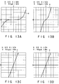
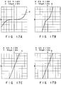
- the current-voltage characteristic of this p-electrode is shown by line A in FIG. 2. As seen from the FIGURE, this p-type electrode establishes a good ohmic contact with the p-type gallium nitride-based III-V Group compound semiconductor.
- the light-emitting device of the present invention having a light-transmissive, ohmic p-electrode 15 allows to observe the light emitted therefrom through the p-electrode 15. Therefore, as shown in FIG. 1, the device can be mounted on a cup-type lead frame 18 which is generally used for mounting a light-emitting device utilizing semiconductors other than gallium nitride-based III-V Group compound semiconductors. As shown, the bottom surface of the substrate, on which no semiconductor layers are formed, i.e., a second major surface 11b opposite to the major surface 11a, is directed to the lead frame 18.
- the p-type electrode 15 is connected with a bonding wire 21, such as a gold wire, at a bonding pad 17 formed on a portion of the surface of the p-type electrode 15.
- the bonding wire is, in turn, connected with a separate lead frame (metal post) 19.
- the n-electrode 14 is connected with the cup-like lead frame 18 through a bonding wire 20, such as a gold wire.
- the bonding pad 17 is preferably formed of gold alone, or a metallic material containing at least two metals including gold, and not containing aluminum or chromium.
- a metallic material may preferably comprise gold, and titanium, nickel, indium and/or platinum. These metallic materials exhibit a good adhesion with the p-electrode 13, and also exhibit a good adhesion with a metallic ball formed from a bonding wire during the wire bonding. Further, these metallic materials do not migrate into the p-electrode to degrade it (reduce the light-transmissivity) during the annealing treatment or during the application of the current to the device to emit light.
- a metallic material containing chromium or aluminum migrates into the p-electrode in a relatively short period of time (for example, 500 hours) during the application of the current, degrading the p-electrode.
- a bonding pad was formed on a p-electrode 15 of the device, as shown in FIG. 1, having a sapphire substrate as the substrate 15, a 4 ⁇ m thick n-type GaN layer as the n-type semiconductor layer 12, and a 1 ⁇ m thick p-type GaN layer doped with magnesium as the p-type semiconductor layer 13.
- the p-electrode 15 was produced by forming a nickel layer to a thickness of 0.1 ⁇ m and then a gold layer to a thickness of 0.1 ⁇ m, and annealing these layers at 600°C to alloy them and render the electrode light-transmissive. The thickness of the p-electrode thus formed was 0.05 ⁇ m.
- Each bonding pad was formed from each of various metallic materials shown in Table 1 below such that a layer of a metal on the row of Table 1 was vapor-deposited directly on the p-electrode, and a layer of a metal on the line of Table 1 was vapor-deposited thereon. These metal layers were annealed simultaneously with the annealing of the p-electrode.
- the bonding wire was a gold wire.
- VG stands for "very good”
- G stands for “good”
- G indicates that the portion of the p-electrode around the bonding pad is slightly color-changed, but not significantly attenuating the light form the device, and the ohmic property between the p-electrode and the p-type semiconductor layer was not changed.
- the symbol, B stands for "bad", and indicates that the light-transmissivity of the p-electrode was lost, and also the ohmic property between the p-electrode and the p-type semiconductor layer was lost.
- the symbol "-" indicates that the bonding pad was poor in adhesion with the gold ball, and thus the wire bonding was difficult to perform.
- the bonding pad is formed of the same metallic material as the p-electrode, i.e., Ni-Au, the p-electrode is not color-changed at all, and maintains the initial light-transmissivity.
- the bonding pad is formed of gold.
- Cr or Al readily migrated into the p-electrode to degrade the characteristics of the p-electrode, even if gold was contained therein.
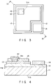
- FIG. 3 is a plan view of a semiconductor light-emitting device according to a second embodiment of the present invention.
- FIG. 4 is an enlarged cross-sectional view, taken along the line IV-IV of FIG. 3.
- This embodiment relates to an improvement in a bonding pad for the p-electrode.
- a cut-off portion 311 is provided in the p-electrode 15, exposing a portion of the surface of the p-type semiconductor layer 13.
- a bonding pad 32 strongly adheres to the p-type semiconductor layer 13 through the cut-off portion 311, and is electrically connected with the p-electrode 15.
- the bonding pad 32 not only fills the cut-off portion 311, but also extends over a portion of the p-electrode 15 around the cut-off portion 311.
- the cut-off portion 311, and hence the bonding pad 32 are arranged farthest from the n-electrode 14 provided on the n-type semiconductor layer 12 (the same also applies to the device of FIG. 1). With such an arrangement, the applied current can spread throughout the entire p-type semiconductor layer 13 to obtain a uniform light output from the device.
- the cut-off portion (window) 311 is arranged at a corner portion of the light-transmissive p-electrode 15, and the n-electrode 14 is arranged at an opposite corner portion of the n-type semiconductor layer 12, on a diagonal line of the square wafer.
- the bonding pad 32 may be formed of a metallic material which does not form an ohmic contact with the p-type semiconductor layer 13, though it may be formed of a metallic material establishing such an ohmic contact.
- the bonding pad 32 should be formed of a metallic material which adheres to the p-type semiconductor layer 13 more strongly than the p-electrode 15.
- the bonding pad 32 adheres to the p-type semiconductor layer 13 more strongly than the p-electrode 15, the bonding pad 13 and/or the p-electrode 15 is prevented from peeling off the substrate, even if the bonding pad 32 is pulled by a bonding wire, such as a gold wire, during the wire bonding operation.
- a material for the bonding pad includes aluminum alone, or a metallic material containing at least two metals selected from the group consisting of chromium, aluminum and gold.
- these metals may be alloyed in advance, or the metallic material may comprises a layer of one metal, and a layer of the other metal stacked thereon, as mentioned before.
- the metals in the multi-layered structure can be simultaneously alloyed at time of the annealing treatment conducted on the p-electrode 15.
- These metallic materials may not establish a good ohmic contact with the p-type semiconductor layer 13, but strongly adheres to the p-type semiconductor material, and does not peel off from the wafer during the wire bonding operation. Therefore, these metallic materials may have so small a thickness as to be light-transmissive. Such a thin film bonding pad transmits the light emitted from the device therethrough, and does not significantly reduce the light output of the device.
- the bonding pad 32 may be of a multi-layered structure in which a layer directly contacting the p-electrode 15 is formed of a metallic material which more strongly adheres to the p-type semiconductor layer 13, and the uppermost layer is formed of a metal which more strongly adheres to the material forming the bonding wire.
- 1,000 light-transmissive bonding pads were prepared on a p-type GaN layer by sequentially vapor-depositing a nickel layer and then a gold layer to a total thickness of 0.01 ⁇ m.
- each of Cr-Al, Al-Au, Cr-Au, and Al alone was vapor-deposited on a p-type GaN layer to a total thickness of 0.01 ⁇ m to provide 1,000 bonding pads on each p-type GaN layer.
- the bonding pads were bonded with corresponding gold wires, and the number of bonding pads which were peeled off, when the gold wires were released, was counted to determine the yield of the bonding pads.
- the yield of the bonding pads formed of Ni-Au was about 60%, but the yield of each of the other bonding pads was 98% or more.
- the bonding strength with the p-type semiconductor layer 13 may be enhanced by making larger the thickness of the bonding pad 32.
- the thick bonding pad does not exhibit light-transmissivity, but may form an ohmic contact if formed of the same material as the p-electrode.
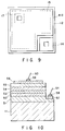
- FIG. 5 shows a device similar to the device of FIG. 4, except that a cut-off portion 312 is provided such that a corner portion of the light-transmitting p-electrode 15 is cut away.
- the bonding pad filling the cut-off portion 312 is not shown, in order to clearly illustrate the cut-off portion 312.
- FIG. 6 illustrate a light-emitting device according to a third embodiment of the invention, and shows a structure similar to the device of FIG. 1, except that an electrically insulating, transparent protective film (protective film 411) covers the thin, light-transmissive p-electrode 15.
- the protective film has a transparency such that it may transmit 90% or more of the light therethrough.
- the protective film is insulative, and thus prevents short-circuiting between the p-electrode 15 and the metallic ball that is formed on the n-electrode 14 during the wire bonding operation and remains there, even if the metallic ball is contacted with the p-electrode 15. Further, the protective film is transparent, and thus transmits the light emitted from the device therethrough.
- the protective film does not reduce the external quantum efficiency of the device. Further, the protective film protects the thin p-electrode 15 from being scratched, and prevents the bonding pad 17 or the p-electrode 15 from peeling off, even when pulled by the bonding wire during the wire bonding operation.
- the material forming the protective film is not particularly limited, as long as it is transparent, and electrically insulative.
- a preferable material includes silicon oxide, titanium oxide, aluminum oxide, or silicon nitride. These materials are colorless, transparent, regardless of how thick it is formed, and are electrically insulative. Therefore, the protective films made of these materials does not substantially attenuate the light emitted from the device.
- the protective film can be formed by the conventional vapor deposition or sputtering technique.
- the thickness of the protective film is not particularly limited, but is usually 0.001 ⁇ m to 10 ⁇ m.
- the metallic ball formed from the bonding wire tends to bridge the n-electrode 14 and the p-electrode 15 during the wire bonding operation at a region between the n-electrode 14 and the bonding pad 17. Therefore, the protective film 411 shown in FIG. 6 covers such a region entirely.
- FIG. 7 shows a structure similar to the structure of FIG. 6, except that the protective film (protective film 412) covers the entire exposed surface of the p-electrode 15, the exposed edge surface of the p-type semiconductor layer 13, and the exposed surface of the n-type semiconductor layer 12. Therefore, the reliability of the device shown in FIG. 7 is more improved over that of the device of FIG. 6.
- FIG. 8 shows a structure similar to the structure of FIG. 6, except that the protective film (protective film 413) continuously covers almost entire surface of the wafer excluding a bonding portion of the n-electrode 14, for bonding with a bonding wire, and a bonding portion of the bonding pad 17, for bonding with a bonding wire.
- the protective film 413 also on the surface of the bonding pad 17, the bonding pad 17 becomes further pressed against the p-electrode 15, preventing the bonding pad 17 from peeling off the p-electrode 15.
- the protective film 413 also covers the n-electrode 14, preventing the n-electrode 14 from peeling off the n-type semiconductor layer 12.
- FIG. 9 shows a structure similar to the structure of FIG. 8, except that the n-electrode 14 and the bonding pad 17 are arranged at corner portions opposite to each other on a diagonal line of the square wafer. The advantages described with reference to FIG. 3 can also be obtained by this arrangement.
- An n-electrode according to the present invention is formed of a metallic material comprising titanium, and aluminum and/or gold, such as a metallic material containing titanium and aluminum, a metallic material containing titanium and gold, or a metallic material containing titanium, aluminum and gold. These metals may be alloyed in advance, or the metallic material may be of a multi-layered structure in which layers of the metals are sequentially stacked, as mentioned before.
- the n-electrode formed of such a metallic material establishes an excellent ohmic contact with an n-type gallium nitride-based III-V Group compound semiconductor layer when annealed.
- the annealing temperature is particularly preferably 400°C or more.
- the annealing treatment is preferably conducted for 0.01 to 30 minutes, and under a non-oxidative or inert atmosphere such as nitrogen as described previously.
- a gallium nitride-based III-V Group compound semiconductor has a property to become n-type without doping an n-type dopant thereinto, since nitrogen lattice vacancies are created in the grown crystal.
- the compound semiconductor exhibits a more preferable n-type conductivity when doped with an n-type dopant such as silicon, germanium, selenium, or sulfur.
- Gallium nitride-based III-V Group compound semiconductors are usually grown by a vapor phase growth method such as metalorganic chemical vapor deposition (MOCVD or MOVPE), hydride chemical vapor deposition (HDCVD), or molecular beam epitaxy (MBE).
- MOCVD or MOVPE metalorganic chemical vapor deposition
- HDCVD hydride chemical vapor deposition
- MBE molecular beam epitaxy
- compounds which contains hydrogen atoms, such as trimethylgallium as a gallium source, and ammonia or hydrazine as a nitrogen source, and also hydrogen gas as a carrier gas.
- the gaseous compounds which contain hydrogen atoms are thermally decomposed during the growth of the gallium nitride-based III-V Group compound semiconductor and release hydrogen. The released hydrogen atoms are trapped in the growing compound semiconductor, and combine with the nitrogen lattice vacancies or the n-type or p-type dopant, to inhibit their functions.
- n-electrode material or the p-electrode material is annealed at a temperature of 400°C or more, the hydrogen trapped in the semiconductor crystal is expelled off, to activate the n-type or p-type dopant, thereby effectively increasing the electron carrier concentration or the hole carrier concentration in the semiconductor crystal, and establishing an ohmic contact.
- This effect of annealing is similar to the effect of annealing on a gallium nitride-based III-V Group compound semiconductor doped with a p-type dopant as described in the above-mentioned JP-A-5-183189 or USSN 07/970,145.
- a gallium nitride-based III-V Group compound semiconductor doped with a p-type dopant gradually decreases in its resistivity starting from the annealing at 400°C, and exhibits a constant resistivity when annealed at 700°C or more.
- the resistivity gradually decreases, starting from the annealing at 400°C, but does not show a sharp decrease.
- the n-type semiconductor exhibits a resistivity as low as 1/2 of the initial resistivity by the annealing treatment at 600°C, and no more decreases in its resistivity at a higher temperature.
- the annealing is conducted on the n-electrode material preferably at 500°C or more, and more preferably 600°C or more.
- a lower annealing temperature suffices, with 450°C or more being preferable, and 500°C or more being more preferable.
- the annealing should be conducted at a temperature lower than the decomposition temperature of the gallium nitride-based III-V Group compound semiconductor, as mentioned before.
- the thickness of the n-electrode is not particularly limited, but it is usually 50 angstroms or more, preferably 0.01 ⁇ m to 5 ⁇ m.
- the n-electrode material of the invention comprising titanium, and aluminum and/or gold is preferably of a multi-layered structure in which layers of the metals are sequentially stacked.
- a layer of titanium be provided in direct contact with the n-type gallium nitride-based III-V Group compound semiconductor layer.
- Titanium can form a more preferable ohmic contact with the n-type gallium nitride-based III-V Group compound semiconductor layer.
- the titanium layer is preferably formed to a thickness of 20 angstroms to 0.3 ⁇ m.
- a total thickness of the aluminum and/or gold layer subsequently formed is preferably larger than the thickness of the titanium layer.
- an n-electrode material of the invention comprising titanium and gold, or comprising titanium, gold and aluminum has an anti-oxidation property improved over that of an n-electrode material comprising titanium and aluminum, and strongly adheres to the gold ball formed during the wire bonding.
- an n-electrode material of the invention comprising gold is preferably has a multi-layered structure in which a gold layer constitutes the uppermost layer. Naturally, the gold layer very strongly adheres to the gold ball.
- FIG. 10 illustrates a light-emitting device according to a fourth embodiment of the invention, and shows a device of a double heterostructure having an n-electrode of the invention.
- This device has an n-type gallium nitride-based III-V Group compound semiconductor layer 51 having a thickness of, for example, 1 ⁇ m to 10 ⁇ m, formed over the substrate 11 through a buffer layer (not shown) formed of, for example, an undoped GaN having a thickness of 0.002 ⁇ m to 0.5 ⁇ m.
- a first clad layer 52 is provided, which is formed of an n-type gallium nitride-based III-V Group compound semiconductor, for example, an n-type GaAlN doped with an n-type dopant such as silicon.
- the first clad layer 52 usually has a thickness of 0.01 to 5 ⁇ m, preferably 0.1 to 4 ⁇ m.
- an active layer (light-emitting layer) 53 is provided, which is formed of a gallium nitride-based III-V Group compound semiconductor having a semiconductor composition different from the clad layer 52.
- the active layer 53 is preferably formed of a low-resistivity In a Ga 1-a N, where 0 ⁇ a ⁇ 1, doped with an n-type or p-type dopant, preferably an n-type dopant.
- the active layer 53 has a thickness of 10 angstroms to 0.5 ⁇ m, preferably 0.01 ⁇ m to 0.2 ⁇ m.
- a second clad layer 54 is provided, which is formed of a p-type gallium nitride-based III-V Group compound semiconductor having a semiconductor composition different from the active layer 53, for example, a p-type GaAlN doped with a p-type dopant such as magnesium
- the second clad layer 54 has a thickness of, usually, 0.01 ⁇ m or more, preferably 0.1 ⁇ m to 1 ⁇ m.
- a contact layer 55 is provided, which is formed of a p-type gallium nitride-based III-V Group compound semiconductor such as a p-type GaN.
- a p-electrode 56 is provided on the contact layer 54.
- the p-type electrode 56 may be formed of any suitable, electrically conductive metallic material.
- a p-electrode material that exhibits a good ohmic property includes a metallic material comprising nickel and gold. Nickel and gold may be alloyed in advance. However, the metallic material comprising nickel and gold particularly preferably has a multi-layered structure in which a nickel layer and a gold layer are sequentially stacked. In the latter case, the nickel layer is preferably provided in direct contact with the contact layer 55.
- the light-transmitting p-electrode 15, and further the bonding pad 32 may be applied to the device of FIG. 10.
- the p-electrode 56 is connected with a bonding wire 60 through a metallic ball 59.
- the wafer shown is partially etched away from the contact layer 55 to a surface portion of the n-type semiconductor layer 51 in the direction of the thickness, partially exposing the n-type semiconductor layer 51.
- An n-electrode 57 of the present invention is provided on the exposed surface portion of the n-type semiconductor layer 51.
- the n-electrode 57 is connected with a bonding wire 61 through a metallic ball 58.
- FIG. 11A relates to the 1,000 electrodes formed by depositing titanium and then aluminum at a thickness ratio of 0.01 : 1
- FIG. 11B relates to the 1,000 electrodes formed by depositing an Al-Ti alloy containing 1% by weight of titanium.
- FIG. 11C relates to the 1,000 electrodes formed by depositing titanium alone
- FIG. 11D relates to the 1,000 electrodes formed by depositing aluminum alone.
- FIGS. 11A and 11B show the representative results of the electrodes, respectively.
- the electrodes comprising aluminum and titanium form a good ohmic contact with the n-type GaN layer.
- Each 1,000 electrodes all established a good ohmic contact with the n-type GaN as shown in FIGS. 11A and 11B.
- the electrodes formed of titanium alone or aluminum alone did not provide a good ohmic contact, as shown in FIGS. 11A and 11B, and, of these, only a few electrodes indicated the ohmic characteristics as shown in FIG. 11A or FIG. 11B.
- FIGS. 12A to 12D An n-type Ga 0.9 Al 0.1 N layer having a thickness of 0.2 ⁇ m was formed on a sapphire substrate having a diameter of 2 inches.
- 1,000 n-electrodes having a diameter of 100 ⁇ m were formed by vapor-depositing a multi-layered metallic material comprising a titanium layer and an aluminum layer, with the thickness ratio of the titanium and aluminum layer varied, and annealing them at 450°C.
- the current-voltage characteristics were measured among the electrodes of the same material. The results are shown in FIGS. 12A to 12D.
- FIG. 12A relates to the 1,000 electrodes formed by depositing the titanium layer and then the aluminum layer at a thickness ratio of 0.001 : 1, and FIG.
- FIG. 12B relates to the 1,000 electrodes formed by depositing the aluminum layer and then the titanium layer at a thickness ratio of 0.001 : 1.
- FIG. 12C relates to the 1,000 electrodes formed by depositing the titanium layer and then the aluminum layer at a thickness ratio of 1 : 0.001
- FIG. 12D relates to the 1,000 electrodes formed by depositing the aluminum layer and then the titanium layer at a thickness ratio of 1 : 0.001.
- FIGS. 13A to 13D On an n-type GaAlN layer doped with silicon, a titanium layer having a thickness of 0.03 ⁇ m was first vapor-deposited, then an aluminum layer having a thickness of 0.5 ⁇ m was vapor-deposited, and finally a gold layer having a thickness of 0.5 ⁇ m was vapor-deposited.
- the multi-layered structure was annealed at various temperatures for 5 minutes. The current-voltage characteristics were measured on the electrodes thus obtained. The results are shown by lines A to D in FIGS. 13A to 13D, respectively.
- FIG. 13A relates to the annealing at 300°C
- FIG. 13B relates to the annealing at 400°C
- FIG. 13C relates to the annealing at 500°C
- FIG. 13D relates to the annealing at 600°C.
- the electrode did not exhibit preferable ohmic characteristics with the n-type semiconductor layer, when annealed at 300°C (FIG. 13A), but the electrodes exhibited preferable ohmic characteristics when annealed at 400°C or more (FIG. 13B to FIG. 13D).
- the similar results were obtained when the n-electrode was prepared by depositing an alloy of titanium and aluminum.
- FIGS. 14A to 14D were conducted as in the same manner as in Experiment 8, except that a titanium layer having a thickness of 0.03 ⁇ m was vapor-deposited on the n-type GaN layer doped with silicon, and then a gold layer having a thickness of 0.5 ⁇ m was vapor-deposited.
- the results are shown by lines A to D in FIGS. 14A to 14D, respectively.
- FIG. 14A relates to the annealing at 300°C
- FIG. 14B relates to the annealing at 400°C
- FIG. 14C relates to the annealing at 500°C
- FIG. 14D relates to the annealing at 600°C.
- the electrode did not exhibit preferable ohmic characteristics with the n-type semiconductor layer, when annealed at 300°C (FIG. 14A), but the electrodes exhibited preferable ohmic characteristics when annealed at 400°C or more (FIG. 14B to FIG. 14D).
- the similar results were obtained when the n-electrode was prepared by depositing an alloy of titanium and gold.
- the electrodes was subjected to a surface-oxidation by allowing them to stand in air for a day.
- a gold wire 64 was ball-bonded to each electrode 62.
- a gold ball 63 having a diameter of 100 ⁇ m was formed during this operation.
- the ball 63 was clawed with an edged tool 65 from just beside the ball in a horizontal direction, while applying a load, until the ball 63 was peeled off, or crushed without peeling off.
- the results are shown in Table 2.
- Table 2 the value under each load value column indicates the number of the balls peeled off the electrodes. It is indicated “crushed” where the ball was not peeled off, but was crushed.
- the n-electrode formed of titanium and gold, or titanium, aluminum and gold has an anti-oxidation property improved over the electrode formed of titanium and aluminum, and thus exhibits a higher bonding strength with the gold ball. Further, it is seen that, of the n-electrodes formed of titanium, aluminum and gold, a higher adhesion strength can be obtained when the uppermost layer is formed of gold, than when the uppermost layer is formed of aluminum.
- a layer of a high-melting point metallic material having a melting point higher than aluminum includes gold, titanium, nickel, platinum, tungsten, molybdenum, chromium and/or copper, with gold, titanium and/or nickel being most preferred. These materials exhibit a superior adhesion with a first metallic material layer containing titanium and aluminum, and do not separate from the first metallic material layer. Further, these metallic materials strongly bond with the metallic ball formed during the wire bonding.
- the high-melting point metallic material contains gold.
- a particularly preferable high-melting point metallic material contains gold and a high-melting point metallic material other than gold (preferably titanium and/or nickel).
- the high-melting point metallic material may be alloyed in advance, but is preferably of a multi-layered structure in which layers of the metals are sequentially stacked. In the latter case, the uppermost layer is preferably formed of gold, as mentioned before. After the stacked layer structure was formed, an annealing treatment is conducted under the above-mentioned conditions to obtain an n-electrode.
- the high-melting point metallic material prevents the aluminum contained in the underlying, first metallic material from migrating onto the surface, thereby preventing the oxidation of the aluminum.
- FIG. 16 shows an n-electrode 57 of such a multi-layered structure.
- the n-electrode 57 has a fist thin film 57a of a multi-layered structure comprising a titanium layer and an aluminum layer, and formed on the n-type semiconductor layer 51.
- a second thin film of, for example, a multi-layered structure comprising layers of the high-melting point metallic materials is provided on the first thin film 57a.
- FIG. 17A relates to the annealing at 300°C
- FIG. 17B relates to the annealing at 400°C
- FIG. 17C relates to the annealing at 500°C
- FIG. 17D relates to the annealing at 600°C.
- the electrode did not exhibit preferable ohmic characteristics with the n-type semiconductor layer, when annealed at 300°C (FIG. 17A), but the electrodes exhibited preferable ohmic characteristics when annealed at 400°C or more (FIG. 17B to FIG. 17D). It is also seen that the annealing at 600°C did not degrade the ohmic characteristics of the electrode.
- the high-melting point metallic material improves the anti-oxidation property of the metallic material containing titanium and aluminum, and enhances the bonding strength with the gold ball.
- n-electrode of the present invention can be applied as the n-electrode 14 of any of the devices of FIG. 1, and FIGS. 3 to 9, thereby improving their device characteristics.
- a wafer was prepared, which had a buffer layer (thickness: 0.02 ⁇ m) formed of an undoped GaN, an n-type GaN layer (thickness: 4 ⁇ m) doped with silicon, and a p-type GaN layer (thickness: 5 ⁇ m) doped with magnesium, sequentially stacked in the order mentioned on a sapphire substrate. Then, the p-type GaN layer was partially etched away to expose a portion of the surface of the n-type GaN layer.
- the exposed surface portion of the n-type GaN layer was masked. Then, nickel and then gold were vapor-deposited on the entire surface of the p-type GaN layer, to a thickness of 0.03 ⁇ m, and a thickness of 0.07 ⁇ m, respectively. Then, the deposited film was masked, and aluminum was vapor-deposited on the exposed surface portion of the n-type GaN layer after removing the mask thereon.
- the wafer thus obtained was subjected to an annealing treatment at 500°C for 10 minutes, thereby alloying the nickel and gold, and rendering them light-transmissive.
- the p-electrode after the annealing had a thickness of 0.07 ⁇ m, and was light-transmissive.
- One chip was mounted on a cup-like lead frame as shown in FIG. 1, and the predetermined wire bonding operation was performed, to prepare a light-emitting diode.
- the light-emitting output power of this diode was 80 ⁇ W at 20 mA, and the forward voltage was 4 V.
- the number of chips cut out from the wafer was about 16,000.
- the yield of the good quality devices obtained from these chips, excluding the contact-failure devices was 95% or more.
- Chips were cut out from the wafer obtained in Example 1 so that the chip might be mounted on two separate lead frames, with the n-electrode and p-electrode contacted with the corresponding lead frames, respectively, i.e., with the sapphire substrate directed upward in the finished device, as in the prior art.
- the chip size had to be as large as 1 mm square at the minimum.
- the chip obtained was seated astride the two separate lead frames, and the predetermined electrode connections were performed to obtain a light-emitting diode.
- the light-emitting output power of this device was 40 ⁇ W at 20 mA, indicating that the light in the lateral direction was not fully available.
- the number of chips cut out from the wafer was only 2,000, and the yield of the good quality devices obtained from these chips, excluding the contact-failure devices, was only 60%.
- a light-emitting device can be provided, which allows the observation of the light emitted therefrom to be made at the side of the gallium nitride-based III-V Group compound semiconductor layers, because the p-electrode of the invention can establish an ohmic contact with the p-type semiconductor layer, and is light-transmissive, effectively conducting the emitted light outside, without reducing the external quantum efficiency of the device.
- the chip size can be reduced, thus greatly increasing the productivity of the device, the yield of the devices can be enhanced, and the production costs can be reduced.
- Example 1 The same procedures were followed as in Example 1, except that the annealing was performed at 600°C.
- the p-electrode obtained had a thickness substantially the same as that of Example 1, and was light-transmissive, similarly. Further, the light-emitting output power and the forward bias voltage of the light-emitting diode obtained were substantially the same as those of the diode of Example 1. The yield was also the same as in Example 1.
- Example 2 The same procedures were followed as in Example 1, except that a 0.5 ⁇ m thick chromium layer, and then a 0.5 ⁇ m thick nickel layer were vapor-deposited on the p-type GaN layer.
- the p-electrode obtained had a thickness of 0.7 ⁇ m, and similarly light-transmissive. Further, the light-emitting output power and the forward bias voltage of the light-emitting diode obtained were substantially the same as those of the diode of Example 1. The yield was also the same as in Example 1.
- Example 2 The same procedures were followed as in Example 1, except that a 0.01 ⁇ m thick platinum layer, and then a 0.1 ⁇ m thick titanium layer were vapor-deposited on the p-type GaN layer.
- the p-electrode obtained had a thickness of 0.07 ⁇ m, and similarly light-transmissive. Further, the light-emitting output power and the forward bias voltage of the light-emitting diode obtained were substantially the same as those of the diode of Example 1. The yield was also the same as in Example 1.
- a wafer of a double heterostructure was prepared by sequentially growing, on a sapphire substrate having a diameter of 2 inches, a GaN buffer layer, an n-type GaN layer doped with silicon, a first clad layer of GaAlN doped with silicon, an active layer of InGaN doped with zinc and silicon, a second clad layer of GaAlN doped with magnesium, and finally a contact layer of p-type GaN doped with magnesium.
- etching was performed such that one chip will have the structure of FIG. 10, thus partially exposing the n-type GaN layer.
- a 100 angstrom thick titanium layer and then a 0.5 ⁇ m thick gold layer were formed to form a multi-layered film having a diameter of 100 ⁇ m on each exposed portion of the n-type GaN layer.
- the wafer thus obtained, was subjected to an annealing treatment at 600°C for 5 minutes under nitrogen atmosphere, thereby converting each multi-layered film into an n-electrode.
- the current-voltage characteristics of all n-electrode were measured with a wafer prober, and indicated the ohmic characteristics as shown in FIG. 12D.
- Each chip was mounted on a lead frame by the die bonding, and gold wires were bonded to the p- and n-electrodes, respectively, by the ball bonder. Of the 15,000 chips, no n-electrodes were separated from the balls during the ball bonding. Further, twenty chips were sampled at random, and the gold wire of each chip was pulled. All the gold wires were broken before peeling off the n-electrodes.
- 15,000 light-emitting chips were obtained in the same manner as in Example 5, except that a 100 angstrom titanium layer, and then a 0.4 ⁇ m thick aluminum layer were vapor-deposited as the n-electrode material.
- the measurement of the current-voltage characteristics on all the n-electrodes gave the characteristics shown in FIG. 11A.
- no n-electrodes were separated from the balls during the ball bonding.
- twenty chips were sampled at random, and the gold wire of each chip was pulled. All the gold wires were broken before peeling off the n-electrodes.
- 15,000 light-emitting chips were obtained in the same manner as in Example 5, except that a 0.5 ⁇ m thick layer of a Ti-Al alloy containing 1% by weight of titanium was vapor-deposited as the n-electrode material.
- the measurement of the current-voltage characteristics on all the n-electrodes with the wafer prober gave the characteristics shown in FIG. 11B.
- no n-electrodes were separated from the balls during the ball bonding. Further, twenty chips were sampled at random, and the gold wire of each chip was pulled. All the gold wires were broken before peeling off the n-electrodes.
- the light-emitting chip of Example 5 was mounted on two separate lead frames at its p-electrode and n-electrode.
- the p-electrode and n-electrode were adhered to the lead frames with indium adhesives, respectively. After the bonding, the lead frames were pulled. The indium adhesive and the lead frame were separated at the interface therebetween.
- 15,000 light-emitting chips were obtained in the same manner as in Example 5, except that a 100 angstrom thick titanium layer, and then a 0.1 ⁇ m thick aluminum layer were vapor-deposited to form a first thin film, and further a 0.1 ⁇ m thick titanium layer and then a 0.1 ⁇ m thick nickel layer were vapor-deposited as the second thin film.
- the measurement of the current-voltage characteristics on all the n-electrodes with the wafer prober gave the characteristics shown in FIG. 13D.
- no n-electrodes were separated from the balls during the ball bonding. Further, twenty chips were sampled at random, and the gold wire of each chip was pulled. All the gold wires were broken before peeling off the n-electrodes.
- the light-emitting chip of Example 9 was mounted on two separate lead frames at its p-electrode and n-electrode.
- the p-electrode and n-electrode were adhered to the lead frames with indium adhesives, respectively. After the adhesion, the lead frames were pulled. The indium adhesive and the lead frame were separated at the interface therebetween.
- the present invention has been described with reference to specific embodiments. However, the present invention should not be limited thereto, and each embodiment may be applied to the other embodiments where appropriate. Further, the present invention can also be applied to gallium nitride-based III-V Group compound semiconductor light-emitting device of a p-n single heterostructure, in addition to gallium nitride-based III-V Group compound semiconductor light-emitting device of a p-n homojunction structure, or of a double heterostructure.
- the present invention may be applied to not only a light-emitting diode, but also the other light-emitting device such as a light-emitting laser diode, as well as a photodetector having the sensitivity to a wavelength of 600 nm or less, such as a solar cell or a photodiode.
- the present invention provides an electrode material which forms an ohmic contact with a gallium nitride-based III-V Group compound semiconductor, and thus can be applied to any suitable device having a p-type gallium nitride-based III-V Group compound semiconductor layer and/or an n-type gallium nitride-based III-V Group compound semiconductor layer, on a substrate.
- a substrate not only an insulating substrate such as sapphire, but also a semiconductor substrate such as silicon carbide (SiC), silicon (Si), zinc oxide (ZnO), gallium arsenide (GaAs) or gallium phosphide (GaP) may be used.
- SiC silicon carbide
- Si silicon
- ZnO zinc oxide
- GaAs gallium arsenide
- GaP gallium phosphide
Priority Applications (2)
| Application Number | Priority Date | Filing Date | Title |
|---|---|---|---|
| EP04012118A EP1450415A3 (de) | 1993-04-28 | 1994-04-27 | Halbleitervorrichtung aus einer galliumnitridartigen III-V-Halbleiterverbindung |
| EP99114356A EP0952617B1 (de) | 1993-04-28 | 1994-04-27 | Halbleitervorrichtung aus einer galliumnitridartigen III-V-Halbleiterverbindung |
Applications Claiming Priority (24)
| Application Number | Priority Date | Filing Date | Title |
|---|---|---|---|
| JP12489093A JP2803742B2 (ja) | 1993-04-28 | 1993-04-28 | 窒化ガリウム系化合物半導体発光素子及びその電極形成方法 |
| JP12489093 | 1993-04-28 | ||
| JP124890/93 | 1993-04-28 | ||
| JP129313/93 | 1993-05-31 | ||
| JP12931393 | 1993-05-31 | ||
| JP12931393A JP2748818B2 (ja) | 1993-05-31 | 1993-05-31 | 窒化ガリウム系化合物半導体発光素子 |
| JP207274/93 | 1993-07-28 | ||
| JP20727493 | 1993-07-28 | ||
| JP20727493A JP2783349B2 (ja) | 1993-07-28 | 1993-07-28 | n型窒化ガリウム系化合物半導体層の電極及びその形成方法 |
| JP234684/93 | 1993-09-21 | ||
| JP234685/93 | 1993-09-21 | ||
| JP23468593 | 1993-09-21 | ||
| JP23468493A JP2697572B2 (ja) | 1993-09-21 | 1993-09-21 | 窒化ガリウム系化合物半導体発光素子 |
| JP23468593A JP2770717B2 (ja) | 1993-09-21 | 1993-09-21 | 窒化ガリウム系化合物半導体発光素子 |
| JP23468493 | 1993-09-21 | ||
| JP253171/93 | 1993-10-08 | ||
| JP25317193A JP2770720B2 (ja) | 1993-10-08 | 1993-10-08 | 窒化ガリウム系化合物半導体発光素子 |
| JP25317193 | 1993-10-08 | ||
| JP872794 | 1994-01-28 | ||
| JP872694 | 1994-01-28 | ||
| JP872694 | 1994-01-28 | ||
| JP8726/94 | 1994-01-28 | ||
| JP872794A JP3154364B2 (ja) | 1994-01-28 | 1994-01-28 | n型窒化ガリウム系化合物半導体層の電極及びその形成方法 |
| JP8727/94 | 1994-01-28 |
Related Child Applications (1)
| Application Number | Title | Priority Date | Filing Date |
|---|---|---|---|
| EP99114356A Division EP0952617B1 (de) | 1993-04-28 | 1994-04-27 | Halbleitervorrichtung aus einer galliumnitridartigen III-V-Halbleiterverbindung |
Publications (4)
| Publication Number | Publication Date |
|---|---|
| EP0622858A2 true EP0622858A2 (de) | 1994-11-02 |
| EP0622858A3 EP0622858A3 (de) | 1995-05-17 |
| EP0622858B1 EP0622858B1 (de) | 2000-07-12 |
| EP0622858B2 EP0622858B2 (de) | 2004-09-29 |
Family
ID=27571647
Family Applications (3)
| Application Number | Title | Priority Date | Filing Date |
|---|---|---|---|
| EP99114356A Expired - Lifetime EP0952617B1 (de) | 1993-04-28 | 1994-04-27 | Halbleitervorrichtung aus einer galliumnitridartigen III-V-Halbleiterverbindung |
| EP94106587A Expired - Lifetime EP0622858B2 (de) | 1993-04-28 | 1994-04-27 | Halbleitervorrichtung aus einer galliumnitridartigen III-V-Halbleiterverbindung und Verfahren zu ihrer Herstellung |
| EP04012118A Withdrawn EP1450415A3 (de) | 1993-04-28 | 1994-04-27 | Halbleitervorrichtung aus einer galliumnitridartigen III-V-Halbleiterverbindung |
Family Applications Before (1)
| Application Number | Title | Priority Date | Filing Date |
|---|---|---|---|
| EP99114356A Expired - Lifetime EP0952617B1 (de) | 1993-04-28 | 1994-04-27 | Halbleitervorrichtung aus einer galliumnitridartigen III-V-Halbleiterverbindung |
Family Applications After (1)
| Application Number | Title | Priority Date | Filing Date |
|---|---|---|---|
| EP04012118A Withdrawn EP1450415A3 (de) | 1993-04-28 | 1994-04-27 | Halbleitervorrichtung aus einer galliumnitridartigen III-V-Halbleiterverbindung |
Country Status (5)
| Country | Link |
|---|---|
| US (11) | US5563422A (de) |
| EP (3) | EP0952617B1 (de) |
| KR (3) | KR100286699B1 (de) |
| CN (6) | CN1240142C (de) |
| DE (2) | DE69433926T2 (de) |
Cited By (39)
| Publication number | Priority date | Publication date | Assignee | Title |
|---|---|---|---|---|
| EP0834929A2 (de) * | 1996-10-03 | 1998-04-08 | Toyoda Gosei Co., Ltd. | Ohmscher Kontakt zu einer n-GAN verwandten Halbleiterverbindung und dessen Herstellungsmethode |
| US5739554A (en) * | 1995-05-08 | 1998-04-14 | Cree Research, Inc. | Double heterojunction light emitting diode with gallium nitride active layer |
| EP0845818A2 (de) * | 1996-11-29 | 1998-06-03 | Toyoda Gosei Co., Ltd. | Halbleitervorrichtung auf Basis einer Galliumnitrid-Halbleiterverbindung und Verfahren zu ihrer Herstellung |
| WO1998037586A1 (en) * | 1997-02-21 | 1998-08-27 | Hewlett-Packard Company | Method for fabricating low-resistance contacts on nitride semiconductor devices |
| EP0892443A2 (de) * | 1997-07-16 | 1999-01-20 | Sanyo Electric Co., Ltd. | Elektrode für halbleitendes Nitrid vom N-Typ, Halbleiterbauelement mit einer solchen Elektrode und Herstellungsverfahren |
| WO1999010936A2 (en) * | 1997-08-29 | 1999-03-04 | Cree Inc. | Robust group iii nitride light emitting diode for high reliability in standard applications |
| EP0911888A2 (de) * | 1994-03-22 | 1999-04-28 | Toyoda Gosei Co., Ltd. | Lichtemittierende Halbleitervorrichtung, die Stickstoff enthaltende Verbindung der Gruppe III verwendet |
| US6005258A (en) * | 1994-03-22 | 1999-12-21 | Toyoda Gosei Co., Ltd. | Light-emitting semiconductor device using group III Nitrogen compound having emission layer doped with donor and acceptor impurities |
| US6008539A (en) * | 1995-06-16 | 1999-12-28 | Toyoda Gosei Co., Ltd. | Electrodes for p-type group III nitride compound semiconductors |
| US6121127A (en) * | 1996-06-14 | 2000-09-19 | Toyoda Gosei Co., Ltd. | Methods and devices related to electrodes for p-type group III nitride compound semiconductors |
| US6191436B1 (en) | 1995-03-13 | 2001-02-20 | Toyoda Gosei Co., Ltd. | Optical semiconductor device |
| US6459100B1 (en) | 1998-09-16 | 2002-10-01 | Cree, Inc. | Vertical geometry ingan LED |
| DE19820777C2 (de) * | 1997-05-08 | 2003-06-18 | Showa Denko Kk | Elektrode für lichtemittierende Halbleitervorrichtungen |
| EP1320894A1 (de) * | 2000-07-26 | 2003-06-25 | American Xtal Technology, Inc. | VERBESSERTES FENSTER FÜR GaN-LED |
| WO2003098712A2 (en) * | 2002-05-14 | 2003-11-27 | Cree, Inc. | High-reliability group iii-nitride light emitting diode |
| WO2003107443A2 (en) * | 2002-06-17 | 2003-12-24 | Kopin Corporation | Bonding pad for gallium nitride-based light-emitting device |
| EP1424726A1 (de) * | 2001-09-06 | 2004-06-02 | Toyoda Gosei Co., Ltd. | N-elektrode für ein halbleiterelement der gruppe-iii-nitridzusammensetzung |
| US6800501B2 (en) | 1997-05-08 | 2004-10-05 | Showa Denko K.K. | Electrode for light-emitting semiconductor devices and method of producing the electrode |
| US6936859B1 (en) | 1998-05-13 | 2005-08-30 | Toyoda Gosei Co., Ltd. | Light-emitting semiconductor device using group III nitride compound |
| US6952024B2 (en) | 2003-02-13 | 2005-10-04 | Cree, Inc. | Group III nitride LED with silicon carbide cladding layer |
| EP1605523A1 (de) * | 2003-03-14 | 2005-12-14 | SUMITOMO ELECTRIC INDUSTRIES Ltd | Halbleiterbauelement |
| US6987281B2 (en) | 2003-02-13 | 2006-01-17 | Cree, Inc. | Group III nitride contact structures for light emitting devices |
| DE19861007B4 (de) * | 1997-05-08 | 2006-07-13 | Showa Denko K.K. | Elektrode für lichtemittiernde Halbleitervorrichtungen und Verfahren zur Herstellung der Elektrode |
| US7170097B2 (en) | 2003-02-14 | 2007-01-30 | Cree, Inc. | Inverted light emitting diode on conductive substrate |
| DE19921987B4 (de) * | 1998-05-13 | 2007-05-16 | Toyoda Gosei Kk | Licht-Abstrahlende Halbleitervorrichtung mit Gruppe-III-Element-Nitrid-Verbindungen |
| US7358544B2 (en) | 2004-03-31 | 2008-04-15 | Nichia Corporation | Nitride semiconductor light emitting device |
| EP2197022A2 (de) * | 2001-10-22 | 2010-06-16 | LG Electronics Inc. | Verfahren zur Herstellung einer Diode mit einer reflektierenden Schicht |
| US7893452B2 (en) | 2004-09-30 | 2011-02-22 | Osram Opto Semiconductors Gmbh | Optoelectronic component and package for an optoelectronic component |
| EP2290711A2 (de) * | 2008-06-16 | 2011-03-02 | LG Innotek Co., Ltd. | Lichtemittierendes halbleiterbauelement |
| EP1973161A3 (de) * | 2007-03-19 | 2011-03-02 | Seoul Opto Device Co., Ltd. | Lichtemittierende Diode |
| US8101961B2 (en) | 2006-01-25 | 2012-01-24 | Cree, Inc. | Transparent ohmic contacts on light emitting diodes with growth substrates |
| US8759868B2 (en) | 2004-07-27 | 2014-06-24 | Cree, Inc. | Ultra-thin ohmic contacts for p-type nitride light emitting devices |
| US9136424B2 (en) | 2001-07-17 | 2015-09-15 | Lg Innotek Co., Ltd. | Diode having high brightness and method thereof |
| US9257613B2 (en) | 2008-06-16 | 2016-02-09 | Lg Innotek Co., Ltd. | Semiconductor light emitting device |
| US9620677B2 (en) | 2001-10-26 | 2017-04-11 | Lg Innotek Co., Ltd. | Diode having vertical structure |
| US9716213B2 (en) | 2002-06-26 | 2017-07-25 | Lg Innotek Co., Ltd. | Thin film light emitting diode |
| US11112555B2 (en) | 2019-09-30 | 2021-09-07 | Nichia Corporation | Light-emitting module with a plurality of light guide plates and a gap therein |
| US11424217B2 (en) | 2019-08-01 | 2022-08-23 | Infineon Technologies Ag | Soldering a conductor to an aluminum layer |
| US11561338B2 (en) | 2019-09-30 | 2023-01-24 | Nichia Corporation | Light-emitting module |
Families Citing this family (430)
| Publication number | Priority date | Publication date | Assignee | Title |
|---|---|---|---|---|
| AUPQ131399A0 (en) * | 1999-06-30 | 1999-07-22 | Silverbrook Research Pty Ltd | A method and apparatus (NPAGE02) |
| US6277969B1 (en) * | 1991-03-18 | 2001-08-21 | New York University | Anti-TNF antibodies and peptides of human tumor necrosis factor |
| US6440823B1 (en) | 1994-01-27 | 2002-08-27 | Advanced Technology Materials, Inc. | Low defect density (Ga, Al, In)N and HVPE process for making same |
| US6136626A (en) * | 1994-06-09 | 2000-10-24 | Matsushita Electric Industrial Co., Ltd. | Semiconductor light-emitting device and production method thereof |
| EP0772247B1 (de) * | 1994-07-21 | 2004-09-15 | Matsushita Electric Industrial Co., Ltd. | Lichtemittierende halbleitervorrichtung und herstellungsverfahren |
| US5838029A (en) * | 1994-08-22 | 1998-11-17 | Rohm Co., Ltd. | GaN-type light emitting device formed on a silicon substrate |
| US5825052A (en) * | 1994-08-26 | 1998-10-20 | Rohm Co., Ltd. | Semiconductor light emmitting device |
| US6996150B1 (en) | 1994-09-14 | 2006-02-07 | Rohm Co., Ltd. | Semiconductor light emitting device and manufacturing method therefor |
| US6900465B2 (en) * | 1994-12-02 | 2005-05-31 | Nichia Corporation | Nitride semiconductor light-emitting device |
| US5777350A (en) * | 1994-12-02 | 1998-07-07 | Nichia Chemical Industries, Ltd. | Nitride semiconductor light-emitting device |
| US6346720B1 (en) | 1995-02-03 | 2002-02-12 | Sumitomo Chemical Company, Limited | Layered group III-V compound semiconductor, method of manufacturing the same, and light emitting element |
| JP3000877B2 (ja) * | 1995-02-20 | 2000-01-17 | 松下電器産業株式会社 | 金メッキ電極の形成方法、基板及びワイヤボンディング方法 |
| JPH08288544A (ja) * | 1995-04-14 | 1996-11-01 | Toshiba Corp | 半導体発光素子 |
| US5900650A (en) * | 1995-08-31 | 1999-05-04 | Kabushiki Kaisha Toshiba | Semiconductor device and method of manufacturing the same |
| US6121638A (en) * | 1995-09-12 | 2000-09-19 | Kabushiki Kaisha Toshiba | Multi-layer structured nitride-based semiconductor devices |
| US5923058A (en) * | 1995-11-09 | 1999-07-13 | Northrop Grumman Corporation | Aluminum gallium nitride heterojunction bipolar transistor |
| JP2872096B2 (ja) * | 1996-01-19 | 1999-03-17 | 日本電気株式会社 | 低抵抗p型窒化ガリウム系化合物半導体の気相成長方法 |
| JP3448450B2 (ja) * | 1996-04-26 | 2003-09-22 | 三洋電機株式会社 | 発光素子およびその製造方法 |
| JP3292044B2 (ja) * | 1996-05-31 | 2002-06-17 | 豊田合成株式会社 | p伝導形3族窒化物半導体の電極パッド及びそれを有した素子及び素子の製造方法 |
| US5977566A (en) | 1996-06-05 | 1999-11-02 | Kabushiki Kaisha Toshiba | Compound semiconductor light emitter |
| JP3548654B2 (ja) * | 1996-09-08 | 2004-07-28 | 豊田合成株式会社 | 半導体発光素子 |
| US5866925A (en) * | 1997-01-09 | 1999-02-02 | Sandia Corporation | Gallium nitride junction field-effect transistor |
| JP2967743B2 (ja) * | 1997-01-14 | 1999-10-25 | 日本電気株式会社 | n型窒化ガリウム系半導体のコンタクト電極及びその形成方法 |
| US6107644A (en) * | 1997-01-24 | 2000-08-22 | Rohm Co., Ltd. | Semiconductor light emitting device |
| EP0921577A4 (de) | 1997-01-31 | 2007-10-31 | Matsushita Electric Ind Co Ltd | Lichtemittierendes bauelement; halbleiter lichtemittierende vorrichtung, und deren herstellungsverfahren |
| KR100244208B1 (ko) * | 1997-02-12 | 2000-02-01 | 구자홍 | 발광다이오드및그제조방법 |
| JPH10294531A (ja) * | 1997-02-21 | 1998-11-04 | Toshiba Corp | 窒化物化合物半導体発光素子 |
| US6284395B1 (en) | 1997-03-05 | 2001-09-04 | Corning Applied Technologies Corp. | Nitride based semiconductors and devices |
| WO1998042030A1 (fr) * | 1997-03-19 | 1998-09-24 | Sharp Kabushiki Kaisha | Element emetteur de lumiere semi-conducteur |
| TW329058B (en) * | 1997-03-20 | 1998-04-01 | Ind Tech Res Inst | Manufacturing method for P type gallium nitride |
| JP4203132B2 (ja) * | 1997-03-31 | 2008-12-24 | シャープ株式会社 | 発光素子及びその製造方法 |
| US6139629A (en) * | 1997-04-03 | 2000-10-31 | The Regents Of The University Of California | Group III-nitride thin films grown using MBE and bismuth |
| US6069394A (en) * | 1997-04-09 | 2000-05-30 | Matsushita Electronics Corporation | Semiconductor substrate, semiconductor device and method of manufacturing the same |
| US5856217A (en) * | 1997-04-10 | 1999-01-05 | Hughes Electronics Corporation | Modulation-doped field-effect transistors and fabrication processes |
| JP3365607B2 (ja) * | 1997-04-25 | 2003-01-14 | シャープ株式会社 | GaN系化合物半導体装置及びその製造方法 |
| US6420735B2 (en) | 1997-05-07 | 2002-07-16 | Samsung Electronics Co., Ltd. | Surface-emitting light-emitting diode |
| US6100586A (en) * | 1997-05-23 | 2000-08-08 | Agilent Technologies, Inc. | Low voltage-drop electrical contact for gallium (aluminum, indium) nitride |
| US5888886A (en) * | 1997-06-30 | 1999-03-30 | Sdl, Inc. | Method of doping gan layers p-type for device fabrication |
| JPH1140891A (ja) * | 1997-07-15 | 1999-02-12 | Nec Corp | 窒化ガリウム系半導体発光素子及びその製造方法 |
| AU747260B2 (en) | 1997-07-25 | 2002-05-09 | Nichia Chemical Industries, Ltd. | Nitride semiconductor device |
| JP3457511B2 (ja) * | 1997-07-30 | 2003-10-20 | 株式会社東芝 | 半導体装置及びその製造方法 |
| US5886401A (en) * | 1997-09-02 | 1999-03-23 | General Electric Company | Structure and fabrication method for interconnecting light emitting diodes with metallization extending through vias in a polymer film overlying the light emitting diodes |
| JPH1187850A (ja) | 1997-09-03 | 1999-03-30 | Sharp Corp | 窒化物系化合物半導体レーザ素子及びレーザ装置 |
| FR2769924B1 (fr) | 1997-10-20 | 2000-03-10 | Centre Nat Rech Scient | Procede de realisation d'une couche epitaxiale de nitrure de gallium, couche epitaxiale de nitrure de gallium et composant optoelectronique muni d'une telle couche |
| US6555452B2 (en) | 1997-11-18 | 2003-04-29 | Technologies And Devices International, Inc. | Method for growing p-type III-V compound material utilizing HVPE techniques |
| US6472300B2 (en) | 1997-11-18 | 2002-10-29 | Technologies And Devices International, Inc. | Method for growing p-n homojunction-based structures utilizing HVPE techniques |
| US6890809B2 (en) * | 1997-11-18 | 2005-05-10 | Technologies And Deviles International, Inc. | Method for fabricating a P-N heterojunction device utilizing HVPE grown III-V compound layers and resultant device |
| US6599133B2 (en) | 1997-11-18 | 2003-07-29 | Technologies And Devices International, Inc. | Method for growing III-V compound semiconductor structures with an integral non-continuous quantum dot layer utilizing HVPE techniques |
| US6849862B2 (en) * | 1997-11-18 | 2005-02-01 | Technologies And Devices International, Inc. | III-V compound semiconductor device with an AlxByInzGa1-x-y-zN1-a-bPaAsb non-continuous quantum dot layer |
| US6559467B2 (en) | 1997-11-18 | 2003-05-06 | Technologies And Devices International, Inc. | P-n heterojunction-based structures utilizing HVPE grown III-V compound layers |
| US6479839B2 (en) | 1997-11-18 | 2002-11-12 | Technologies & Devices International, Inc. | III-V compounds semiconductor device with an AlxByInzGa1-x-y-zN non continuous quantum dot layer |
| US6559038B2 (en) | 1997-11-18 | 2003-05-06 | Technologies And Devices International, Inc. | Method for growing p-n heterojunction-based structures utilizing HVPE techniques |
| US6476420B2 (en) * | 1997-11-18 | 2002-11-05 | Technologies And Devices International, Inc. | P-N homojunction-based structures utilizing HVPE growth III-V compound layers |
| US20020047135A1 (en) * | 1997-11-18 | 2002-04-25 | Nikolaev Audrey E. | P-N junction-based structures utilizing HVPE grown III-V compound layers |
| US8587020B2 (en) | 1997-11-19 | 2013-11-19 | Epistar Corporation | LED lamps |
| US6633120B2 (en) * | 1998-11-19 | 2003-10-14 | Unisplay S.A. | LED lamps |
| DE69839300T2 (de) * | 1997-12-15 | 2009-04-16 | Philips Lumileds Lighting Company, LLC, San Jose | Licht-emittierende Vorrichtung |
| KR19990052640A (ko) | 1997-12-23 | 1999-07-15 | 김효근 | 오믹접촉 형성을 이용한 다이오드용 금속박막및 그의 제조방법 |
| US5998232A (en) * | 1998-01-16 | 1999-12-07 | Implant Sciences Corporation | Planar technology for producing light-emitting devices |
| JPH11274468A (ja) * | 1998-03-25 | 1999-10-08 | Sony Corp | オーミック電極およびその形成方法ならびにオーミック電極形成用積層体 |
| US6319742B1 (en) * | 1998-07-29 | 2001-11-20 | Sanyo Electric Co., Ltd. | Method of forming nitride based semiconductor layer |
| JP3785820B2 (ja) * | 1998-08-03 | 2006-06-14 | 豊田合成株式会社 | 発光装置 |
| US6169298B1 (en) * | 1998-08-10 | 2001-01-02 | Kingmax Technology Inc. | Semiconductor light emitting device with conductive window layer |
| WO2000017941A1 (fr) | 1998-09-18 | 2000-03-30 | Mitsubishi Cable Industries, Ltd. | Photodetecteur a semi-conducteur |
| TW386286B (en) * | 1998-10-26 | 2000-04-01 | Ind Tech Res Inst | An ohmic contact of semiconductor and the manufacturing method |
| JP2000208800A (ja) * | 1998-11-13 | 2000-07-28 | Fuji Xerox Co Ltd | 太陽電池及びそれを用いた自己電力供給型表示素子、並びに太陽電池の製造方法 |
| US6307218B1 (en) * | 1998-11-20 | 2001-10-23 | Lumileds Lighting, U.S., Llc | Electrode structures for light emitting devices |
| JP2000164938A (ja) * | 1998-11-27 | 2000-06-16 | Sharp Corp | 発光装置及び発光素子の実装方法 |
| DE19904378B4 (de) | 1999-02-03 | 2006-10-05 | Osram Opto Semiconductors Gmbh | Verfahren zur Herstellung von Nitrid-Einkristallen |
| JP3770014B2 (ja) | 1999-02-09 | 2006-04-26 | 日亜化学工業株式会社 | 窒化物半導体素子 |
| EP1168539B1 (de) * | 1999-03-04 | 2009-12-16 | Nichia Corporation | Nitridhalbleiterlaserelement |
| US8664030B2 (en) * | 1999-03-30 | 2014-03-04 | Daniel Luch | Collector grid and interconnect structures for photovoltaic arrays and modules |
| US6813039B1 (en) * | 1999-05-25 | 2004-11-02 | Silverbrook Research Pty Ltd | Method and system for accessing the internet |
| US6287947B1 (en) * | 1999-06-08 | 2001-09-11 | Lumileds Lighting, U.S. Llc | Method of forming transparent contacts to a p-type GaN layer |
| US6521521B1 (en) * | 1999-06-18 | 2003-02-18 | Fu Sheng Industrial Co., Ltd. | Bonding pad structure and method for fabricating the same |
| WO2001002939A1 (en) * | 1999-06-30 | 2001-01-11 | Silverbrook Research Pty Ltd | Method and system for collaborative document markup |
| JP4126812B2 (ja) * | 1999-07-07 | 2008-07-30 | 富士ゼロックス株式会社 | 光半導体素子 |
| JP2001111074A (ja) * | 1999-08-03 | 2001-04-20 | Fuji Xerox Co Ltd | 半導体素子及び太陽電池 |
| JP2001053339A (ja) * | 1999-08-11 | 2001-02-23 | Toshiba Corp | 半導体発光素子およびその製造方法 |
| US6563144B2 (en) | 1999-09-01 | 2003-05-13 | The Regents Of The University Of California | Process for growing epitaxial gallium nitride and composite wafers |
| JP2001144331A (ja) * | 1999-09-02 | 2001-05-25 | Toyoda Gosei Co Ltd | 発光装置 |
| GB2354108B (en) * | 1999-09-08 | 2001-08-08 | Arima Optoelectronics Corp | An isoelectronic co-doping method |
| US6812502B1 (en) | 1999-11-04 | 2004-11-02 | Uni Light Technology Incorporation | Flip-chip light-emitting device |
| US6492661B1 (en) | 1999-11-04 | 2002-12-10 | Fen-Ren Chien | Light emitting semiconductor device having reflection layer structure |
| DE19954319C1 (de) * | 1999-11-11 | 2001-05-03 | Vishay Semiconductor Gmbh | Verfahren zum Herstellen von mehrschichtigen Kontaktelektroden für Verbindungshalbeiter und Anordnung |
| US6614056B1 (en) | 1999-12-01 | 2003-09-02 | Cree Lighting Company | Scalable led with improved current spreading structures |
| US6515313B1 (en) * | 1999-12-02 | 2003-02-04 | Cree Lighting Company | High efficiency light emitters with reduced polarization-induced charges |
| US6646292B2 (en) | 1999-12-22 | 2003-11-11 | Lumileds Lighting, U.S., Llc | Semiconductor light emitting device and method |
| US6514782B1 (en) | 1999-12-22 | 2003-02-04 | Lumileds Lighting, U.S., Llc | Method of making a III-nitride light-emitting device with increased light generating capability |
| US6885035B2 (en) | 1999-12-22 | 2005-04-26 | Lumileds Lighting U.S., Llc | Multi-chip semiconductor LED assembly |
| US6573537B1 (en) | 1999-12-22 | 2003-06-03 | Lumileds Lighting, U.S., Llc | Highly reflective ohmic contacts to III-nitride flip-chip LEDs |
| US6903376B2 (en) * | 1999-12-22 | 2005-06-07 | Lumileds Lighting U.S., Llc | Selective placement of quantum wells in flipchip light emitting diodes for improved light extraction |
| US6486499B1 (en) | 1999-12-22 | 2002-11-26 | Lumileds Lighting U.S., Llc | III-nitride light-emitting device with increased light generating capability |
| US6602701B2 (en) * | 2000-01-11 | 2003-08-05 | The General Hospital Corporation | Three-dimensional cell growth assay |
| WO2001061765A1 (de) * | 2000-02-15 | 2001-08-23 | Osram Opto Semiconductors Gmbh | Strahlungsemittierendes halbleiterbauelement und verfahren zu dessen herstellung |
| DE10006738C2 (de) | 2000-02-15 | 2002-01-17 | Osram Opto Semiconductors Gmbh | Lichtemittierendes Bauelement mit verbesserter Lichtauskopplung und Verfahren zu seiner Herstellung |
| JP4026294B2 (ja) * | 2000-03-07 | 2007-12-26 | 豊田合成株式会社 | Iii族窒化物系化合物半導体素子の製造方法 |
| JP2001267555A (ja) * | 2000-03-22 | 2001-09-28 | Matsushita Electric Ind Co Ltd | 半導体装置及びその製造方法 |
| JP3846150B2 (ja) * | 2000-03-27 | 2006-11-15 | 豊田合成株式会社 | Iii族窒化物系化合物半導体素子および電極形成方法 |
| US7304325B2 (en) * | 2000-05-01 | 2007-12-04 | Toyoda Gosei Co., Ltd. | Group III nitride compound semiconductor light-emitting device |
| GB2362263A (en) * | 2000-05-12 | 2001-11-14 | Juses Chao | Amorphous and polycrystalline growth of gallium nitride-based semiconductors |
| DE20111659U1 (de) * | 2000-05-23 | 2001-12-13 | Osram Opto Semiconductors Gmbh | Bauelement für die Optoelektronik |
| JP3285341B2 (ja) * | 2000-06-01 | 2002-05-27 | 士郎 酒井 | 窒化ガリウム系化合物半導体の製造方法 |
| US6693352B1 (en) | 2000-06-05 | 2004-02-17 | Emitronix Inc. | Contact structure for group III-V semiconductor devices and method of producing the same |
| US6410940B1 (en) * | 2000-06-15 | 2002-06-25 | Kansas State University Research Foundation | Micro-size LED and detector arrays for minidisplay, hyper-bright light emitting diodes, lighting, and UV detector and imaging sensor applications |
| US6303485B1 (en) * | 2000-06-21 | 2001-10-16 | Arima Optoelectronics Corp. | Method of producing gallium nitride-based III-V Group compound semiconductor device |
| US6344665B1 (en) * | 2000-06-23 | 2002-02-05 | Arima Optoelectronics Corp. | Electrode structure of compound semiconductor device |
| US6897494B1 (en) * | 2000-07-26 | 2005-05-24 | Dalian Luming Science And Technology Group Co. Ltd. | GaN light emitting diode with conductive outer layer |
| JP2002043619A (ja) * | 2000-07-27 | 2002-02-08 | Shiro Sakai | 窒化ガリウム系化合物半導体素子の製造方法 |
| TW451504B (en) * | 2000-07-28 | 2001-08-21 | Opto Tech Corp | Compound semiconductor device and method for making the same |
| US6946685B1 (en) | 2000-08-31 | 2005-09-20 | Lumileds Lighting U.S., Llc | Light emitting semiconductor method and device |
| US6248608B1 (en) | 2000-08-31 | 2001-06-19 | Formosa Epitaxy Incorporation | Manufacturing method of a gallium nitride-based blue light emitting diode (LED) ohmic electrodes |
| US6255129B1 (en) * | 2000-09-07 | 2001-07-03 | Highlink Technology Corporation | Light-emitting diode device and method of manufacturing the same |
| DE10044500A1 (de) * | 2000-09-08 | 2002-04-04 | Highlink Technology Corp Chupe | Licht emittierendes Verbindungshalbleiter-Bauteil und Verfahren zur Herstellung desselben |
| CN1333467C (zh) * | 2000-09-13 | 2007-08-22 | 晶元光电股份有限公司 | 白色发光二极管 |
| JP3466144B2 (ja) * | 2000-09-22 | 2003-11-10 | 士郎 酒井 | 半導体の表面を荒くする方法 |
| US6642548B1 (en) | 2000-10-20 | 2003-11-04 | Emcore Corporation | Light-emitting diodes with loop and strip electrodes and with wide medial sections |
| US6653215B1 (en) | 2000-10-05 | 2003-11-25 | Emcore Corporation | Contact to n-GaN with Au termination |
| AU2002211652A1 (en) * | 2000-10-13 | 2002-04-22 | Emcore Corporation | Method of making an electrode |
| WO2002041364A2 (en) * | 2000-11-16 | 2002-05-23 | Emcore Corporation | Led packages having improved light extraction |
| US6888171B2 (en) * | 2000-12-22 | 2005-05-03 | Dallan Luming Science & Technology Group Co., Ltd. | Light emitting diode |
| US7118756B2 (en) * | 2000-12-28 | 2006-10-10 | Wyeth | Recombinant protective protein from Streptococcus pneumoniae |
| US6712478B2 (en) * | 2001-01-19 | 2004-03-30 | South Epitaxy Corporation | Light emitting diode |
| TW488088B (en) * | 2001-01-19 | 2002-05-21 | South Epitaxy Corp | Light emitting diode structure |
| JP2002222992A (ja) * | 2001-01-25 | 2002-08-09 | Rohm Co Ltd | Led発光素子、およびled発光装置 |
| US6794684B2 (en) | 2001-02-01 | 2004-09-21 | Cree, Inc. | Reflective ohmic contacts for silicon carbide including a layer consisting essentially of nickel, methods of fabricating same, and light emitting devices including the same |
| US6791119B2 (en) | 2001-02-01 | 2004-09-14 | Cree, Inc. | Light emitting diodes including modifications for light extraction |
| US20040113168A1 (en) * | 2001-02-21 | 2004-06-17 | Ivan Eliashevich | Light extraction efficiency of gan based leds |
| US6541800B2 (en) | 2001-02-22 | 2003-04-01 | Weldon Technologies, Inc. | High power LED |
| EP1251331B1 (de) | 2001-04-18 | 2012-03-07 | Leica Geosystems AG | Geodätisches Messgerät |
| US6630689B2 (en) | 2001-05-09 | 2003-10-07 | Lumileds Lighting, U.S. Llc | Semiconductor LED flip-chip with high reflectivity dielectric coating on the mesa |
| US6649942B2 (en) | 2001-05-23 | 2003-11-18 | Sanyo Electric Co., Ltd. | Nitride-based semiconductor light-emitting device |
| JP3912044B2 (ja) * | 2001-06-06 | 2007-05-09 | 豊田合成株式会社 | Iii族窒化物系化合物半導体発光素子の製造方法 |
| JP3765246B2 (ja) | 2001-06-06 | 2006-04-12 | 豊田合成株式会社 | Iii族窒化物系化合物半導体発光素子の製造方法 |
| JP3791765B2 (ja) * | 2001-06-08 | 2006-06-28 | 豊田合成株式会社 | Iii族窒化物系化合物半導体発光素子 |
| JP3548735B2 (ja) * | 2001-06-29 | 2004-07-28 | 士郎 酒井 | 窒化ガリウム系化合物半導体の製造方法 |
| US7211833B2 (en) | 2001-07-23 | 2007-05-01 | Cree, Inc. | Light emitting diodes including barrier layers/sublayers |
| US6740906B2 (en) | 2001-07-23 | 2004-05-25 | Cree, Inc. | Light emitting diodes including modifications for submount bonding |
| JP3812827B2 (ja) * | 2001-08-23 | 2006-08-23 | ソニー株式会社 | 発光素子の取り付け方法 |
| JP2003168823A (ja) | 2001-09-18 | 2003-06-13 | Toyoda Gosei Co Ltd | Iii族窒化物系化合物半導体発光素子 |
| DE10147887C2 (de) * | 2001-09-28 | 2003-10-23 | Osram Opto Semiconductors Gmbh | Strahlungsemittierendes Halbleiterbauelement mit einem Kontakt, der eine Mehrzahl von voneinander beabstandeten Kontaktstellen umfaßt |
| DE10152922B4 (de) | 2001-10-26 | 2010-05-12 | Osram Opto Semiconductors Gmbh | Nitrid-basierendes Halbleiterbauelement |
| US20030090103A1 (en) * | 2001-11-09 | 2003-05-15 | Thomas Becker | Direct mailing device |
| JP2003168822A (ja) * | 2001-11-30 | 2003-06-13 | Shin Etsu Handotai Co Ltd | 発光素子及びその製造方法 |
| US6858873B2 (en) * | 2002-01-23 | 2005-02-22 | Chia Ta World Co Ltd | Semiconductor diode having a semiconductor die with a substrate and multiple films applied thereover |
| US6635503B2 (en) | 2002-01-28 | 2003-10-21 | Cree, Inc. | Cluster packaging of light emitting diodes |
| US6730941B2 (en) * | 2002-01-30 | 2004-05-04 | Showa Denko Kabushiki Kaisha | Boron phosphide-based semiconductor light-emitting device, production method thereof, and light-emitting diode |
| US6881983B2 (en) * | 2002-02-25 | 2005-04-19 | Kopin Corporation | Efficient light emitting diodes and lasers |
| US7005685B2 (en) * | 2002-02-28 | 2006-02-28 | Shiro Sakai | Gallium-nitride-based compound semiconductor device |
| US6762432B2 (en) * | 2002-04-01 | 2004-07-13 | Micrel, Inc. | Electrical field alignment vernier |
| US20030189215A1 (en) | 2002-04-09 | 2003-10-09 | Jong-Lam Lee | Method of fabricating vertical structure leds |
| US6720570B2 (en) | 2002-04-17 | 2004-04-13 | Tekcore Co., Ltd. | Gallium nitride-based semiconductor light emitting device |
| US6911079B2 (en) * | 2002-04-19 | 2005-06-28 | Kopin Corporation | Method for reducing the resistivity of p-type II-VI and III-V semiconductors |
| US6919585B2 (en) * | 2002-05-17 | 2005-07-19 | Lumei Optoelectronics, Inc. | Light-emitting diode with silicon carbide substrate |
| WO2004042783A2 (en) * | 2002-05-17 | 2004-05-21 | The Regents Of The University Of California | Hafnium nitride buffer layers for growth of gan on silicon |
| US6650018B1 (en) * | 2002-05-24 | 2003-11-18 | Axt, Inc. | High power, high luminous flux light emitting diode and method of making same |
| US7193245B2 (en) * | 2003-09-04 | 2007-03-20 | Lumei Optoelectronics Corporation | High power, high luminous flux light emitting diode and method of making same |
| JP2004006498A (ja) * | 2002-05-31 | 2004-01-08 | Toyoda Gosei Co Ltd | Iii族窒化物系化合物半導体発光素子 |
| US6734091B2 (en) | 2002-06-28 | 2004-05-11 | Kopin Corporation | Electrode for p-type gallium nitride-based semiconductors |
| US7002180B2 (en) | 2002-06-28 | 2006-02-21 | Kopin Corporation | Bonding pad for gallium nitride-based light-emitting device |
| US6955985B2 (en) | 2002-06-28 | 2005-10-18 | Kopin Corporation | Domain epitaxy for thin film growth |
| US20050189651A1 (en) * | 2002-07-25 | 2005-09-01 | Matsushita Elec. Ind. Co. Ltd. | Contact formation method and semiconductor device |
| US6815241B2 (en) * | 2002-09-25 | 2004-11-09 | Cao Group, Inc. | GaN structures having low dislocation density and methods of manufacture |
| US7213942B2 (en) * | 2002-10-24 | 2007-05-08 | Ac Led Lighting, L.L.C. | Light emitting diodes for high AC voltage operation and general lighting |
| US6957899B2 (en) * | 2002-10-24 | 2005-10-25 | Hongxing Jiang | Light emitting diodes for high AC voltage operation and general lighting |
| JP2006506827A (ja) * | 2002-11-16 | 2006-02-23 | エルジー イノテック カンパニー リミテッド | 光デバイス及びその製造方法 |
| US7115896B2 (en) * | 2002-12-04 | 2006-10-03 | Emcore Corporation | Semiconductor structures for gallium nitride-based devices |
| US7071494B2 (en) * | 2002-12-11 | 2006-07-04 | Lumileds Lighting U.S. Llc | Light emitting device with enhanced optical scattering |
| JP2004200209A (ja) * | 2002-12-16 | 2004-07-15 | Fuji Xerox Co Ltd | 電極等の導電パターンの形成方法およびこれを用いた面発光型半導体レーザ並びにその製造方法 |
| TW577184B (en) | 2002-12-26 | 2004-02-21 | Epistar Corp | Light emitting layer having voltage/resistance interdependent layer |
| DE10261425A1 (de) * | 2002-12-30 | 2004-07-22 | Osram Opto Semiconductors Gmbh | Halbleiterlaserdiode |
| DE102004004780B9 (de) | 2003-01-31 | 2019-04-25 | Osram Opto Semiconductors Gmbh | Verfahren zum Herstellen eines Bauelementes mit einem elektrischen Kontaktbereich und Bauelement mit einem elektrischen Kontaktbereich |
| CN2717023Y (zh) * | 2003-02-19 | 2005-08-10 | 日亚化学工业株式会社 | 氮化物半导体元件 |
| US7148417B1 (en) | 2003-03-31 | 2006-12-12 | The United States Of America As Represented By The Administrator Of The National Aeronautics And Space Administration | GaP/silicon tandem solar cell with extended temperature range |
| US6903380B2 (en) | 2003-04-11 | 2005-06-07 | Weldon Technologies, Inc. | High power light emitting diode |
| US7714345B2 (en) * | 2003-04-30 | 2010-05-11 | Cree, Inc. | Light-emitting devices having coplanar electrical contacts adjacent to a substrate surface opposite an active region and methods of forming the same |
| US7087936B2 (en) * | 2003-04-30 | 2006-08-08 | Cree, Inc. | Methods of forming light-emitting devices having an antireflective layer that has a graded index of refraction |
| US7531380B2 (en) * | 2003-04-30 | 2009-05-12 | Cree, Inc. | Methods of forming light-emitting devices having an active region with electrical contacts coupled to opposing surfaces thereof |
| US7412170B1 (en) | 2003-05-29 | 2008-08-12 | Opticomp Corporation | Broad temperature WDM transmitters and receivers for coarse wavelength division multiplexed (CWDM) fiber communication systems |
| US7122841B2 (en) | 2003-06-04 | 2006-10-17 | Kopin Corporation | Bonding pad for gallium nitride-based light-emitting devices |
| KR100593886B1 (ko) * | 2003-06-24 | 2006-07-03 | 삼성전기주식회사 | 질화갈륨계 반도체 발광소자의 제조방법 |
| TWI222759B (en) * | 2003-07-03 | 2004-10-21 | Epitech Corp Ltd | Light emitting diode and method for manufacturing the same |
| JP2005117020A (ja) * | 2003-09-16 | 2005-04-28 | Stanley Electric Co Ltd | 窒化ガリウム系化合物半導体素子とその製造方法 |
| KR100576849B1 (ko) * | 2003-09-19 | 2006-05-10 | 삼성전기주식회사 | 발광소자 및 그 제조방법 |
| KR20050032159A (ko) * | 2003-10-01 | 2005-04-07 | 삼성전기주식회사 | 질화갈륨계 반도체 발광 소자 및 그 제조방법 |
| KR100506736B1 (ko) * | 2003-10-10 | 2005-08-08 | 삼성전기주식회사 | 질화갈륨계 반도체 발광 소자 및 그 제조방법 |
| KR20050035325A (ko) * | 2003-10-10 | 2005-04-18 | 삼성전기주식회사 | 질화물 반도체 발광소자 및 그 제조방법 |
| KR100647278B1 (ko) * | 2003-10-27 | 2006-11-17 | 삼성전자주식회사 | III - V 족 GaN 계 화합물 반도체 및 이에적용되는 p-형 전극 |
| EP1683206A1 (de) * | 2003-11-12 | 2006-07-26 | Cree, Inc. | Lichtemittierende bauelemente mit selbstausgerichtetem ohmschen kontakt und herstellungsverfahren dafür |
| US20090029353A1 (en) * | 2003-12-08 | 2009-01-29 | Maki Wusi C | Molecular detector |
| JP3767863B2 (ja) * | 2003-12-18 | 2006-04-19 | ローム株式会社 | 半導体発光素子およびその製法 |
| KR100506740B1 (ko) * | 2003-12-23 | 2005-08-08 | 삼성전기주식회사 | 질화물 반도체 발광소자 및 그 제조방법 |
| KR100586943B1 (ko) * | 2003-12-26 | 2006-06-07 | 삼성전기주식회사 | 질화갈륨계 반도체 발광소자의 제조방법 |
| KR100585919B1 (ko) * | 2004-01-15 | 2006-06-01 | 학교법인 포항공과대학교 | 질화갈륨계 ⅲⅴ족 화합물 반도체 소자 및 그 제조방법 |
| US20050179042A1 (en) * | 2004-02-13 | 2005-08-18 | Kopin Corporation | Monolithic integration and enhanced light extraction in gallium nitride-based light-emitting devices |
| US20050179046A1 (en) * | 2004-02-13 | 2005-08-18 | Kopin Corporation | P-type electrodes in gallium nitride-based light-emitting devices |
| KR100541102B1 (ko) * | 2004-02-13 | 2006-01-11 | 삼성전기주식회사 | 오믹 접촉을 개선한 질화물 반도체 발광소자 및 그 제조방법 |
| US7084475B2 (en) * | 2004-02-17 | 2006-08-01 | Velox Semiconductor Corporation | Lateral conduction Schottky diode with plural mesas |
| US7253015B2 (en) * | 2004-02-17 | 2007-08-07 | Velox Semiconductor Corporation | Low doped layer for nitride-based semiconductor device |
| US20070170461A1 (en) * | 2004-02-24 | 2007-07-26 | Koji Kamei | Gallium nitride-based compound semiconductor light-emitting device |
| KR101039997B1 (ko) * | 2004-03-02 | 2011-06-09 | 엘지이노텍 주식회사 | n-ZnO/p-GaAs 이종접합 포토 다이오드 및 그제조방법 |
| KR100486614B1 (ko) * | 2004-03-05 | 2005-05-03 | 에피밸리 주식회사 | 낮은 접촉저항을 가지는 ⅲ-질화물반도체 발광소자 |
| KR100601945B1 (ko) * | 2004-03-10 | 2006-07-14 | 삼성전자주식회사 | 탑에미트형 질화물계 발광소자 및 그 제조방법 |
| KR20050093319A (ko) * | 2004-03-18 | 2005-09-23 | 삼성전기주식회사 | 발광효율이 개선된 질화물 반도체 발광소자 및 그 제조방법 |
| KR100486177B1 (ko) * | 2004-03-25 | 2005-05-06 | 에피밸리 주식회사 | Ⅲ-질화물 반도체 발광소자 |
| KR20050095721A (ko) * | 2004-03-27 | 2005-09-30 | 삼성전자주식회사 | III - V 족 GaN 계 화합물 반도체 발광소자 및 그제조방법 |
| KR100586955B1 (ko) | 2004-03-31 | 2006-06-07 | 삼성전기주식회사 | 질화물 반도체 발광소자의 제조방법 |
| WO2005117151A1 (en) * | 2004-05-26 | 2005-12-08 | Showa Denko K.K. | Positive electrode structure and gallium nitride-based compound semiconductor light-emitting device |
| US7268063B1 (en) * | 2004-06-01 | 2007-09-11 | University Of Central Florida | Process for fabricating semiconductor component |
| US7417266B1 (en) | 2004-06-10 | 2008-08-26 | Qspeed Semiconductor Inc. | MOSFET having a JFET embedded as a body diode |
| CN100550441C (zh) * | 2004-06-24 | 2009-10-14 | 昭和电工株式会社 | 反射性正电极和使用其的氮化镓基化合物半导体发光器件 |
| US7022597B2 (en) * | 2004-07-16 | 2006-04-04 | Tekcore Co., Ltd. | Method for manufacturing gallium nitride based transparent conductive oxidized film ohmic electrodes |
| CN100557829C (zh) * | 2004-07-27 | 2009-11-04 | 克里公司 | 用于p型氮化物发光装置的超薄欧姆接触及其形成方法 |
| WO2006011672A1 (en) * | 2004-07-29 | 2006-02-02 | Showa Denko K.K. | Positive electrode for semiconductor light-emitting device |
| TWI278126B (en) * | 2004-08-04 | 2007-04-01 | Formosa Epitaxy Inc | GaN series light emitting diode structure of p-type contacting layer with low-temperature growth low resistivity |
| US7498611B2 (en) * | 2004-08-05 | 2009-03-03 | Showa Denko K.K. | Transparent electrode for semiconductor light-emitting device |
| CN100485886C (zh) * | 2004-08-09 | 2009-05-06 | 中国科学院微电子研究所 | 适用于氮化镓器件的铝/钛/铝/钛/铂/金的欧姆接触系统 |
| CN100481346C (zh) * | 2004-08-09 | 2009-04-22 | 中国科学院微电子研究所 | 适用于氮化镓器件的铝/钛/铝/镍/金欧姆接触系统 |
| US20060043394A1 (en) * | 2004-09-01 | 2006-03-02 | Liang-Wen Wu | Gallium-nitride based light emitting diode structure |
| JPWO2006028118A1 (ja) * | 2004-09-08 | 2008-05-08 | ローム株式会社 | 半導体発光素子 |
| KR100533645B1 (ko) * | 2004-09-13 | 2005-12-06 | 삼성전기주식회사 | 발광 효율을 개선한 발광 다이오드 |
| KR100649496B1 (ko) * | 2004-09-14 | 2006-11-24 | 삼성전기주식회사 | 질화물 반도체 발광소자 및 제조방법 |
| US7221277B2 (en) * | 2004-10-05 | 2007-05-22 | Tracking Technologies, Inc. | Radio frequency identification tag and method of making the same |
| KR100657909B1 (ko) * | 2004-11-08 | 2006-12-14 | 삼성전기주식회사 | 화합물 반도체 소자의 전극 형성방법 |
| WO2006057485A1 (en) * | 2004-11-29 | 2006-06-01 | Epivalley Co., Ltd. | Iii-nitride semiconductor light emitting device |
| US7566908B2 (en) * | 2004-11-29 | 2009-07-28 | Yongsheng Zhao | Gan-based and ZnO-based LED |
| CN100369277C (zh) * | 2004-12-28 | 2008-02-13 | 中华映管股份有限公司 | 发光二极管 |
| US7436039B2 (en) * | 2005-01-06 | 2008-10-14 | Velox Semiconductor Corporation | Gallium nitride semiconductor device |
| US7221044B2 (en) | 2005-01-21 | 2007-05-22 | Ac Led Lighting, L.L.C. | Heterogeneous integrated high voltage DC/AC light emitter |
| US7525248B1 (en) | 2005-01-26 | 2009-04-28 | Ac Led Lighting, L.L.C. | Light emitting diode lamp |
| US7951632B1 (en) | 2005-01-26 | 2011-05-31 | University Of Central Florida | Optical device and method of making |
| US7535028B2 (en) * | 2005-02-03 | 2009-05-19 | Ac Led Lighting, L.Lc. | Micro-LED based high voltage AC/DC indicator lamp |
| EP1868251A4 (de) * | 2005-04-08 | 2009-05-27 | Mitsubishi Chem Corp | Halbleiterelement und verfahren zu seiner herstellung |
| KR100638813B1 (ko) * | 2005-04-15 | 2006-10-27 | 삼성전기주식회사 | 플립칩형 질화물 반도체 발광소자 |
| US20060234411A1 (en) * | 2005-04-15 | 2006-10-19 | Samsung Electro-Mechanics Co., Ltd. | Method of manufacturing nitride semiconductor light emitting diode |
| KR100609118B1 (ko) * | 2005-05-03 | 2006-08-08 | 삼성전기주식회사 | 플립 칩 발광다이오드 및 그 제조방법 |
| KR101166922B1 (ko) * | 2005-05-27 | 2012-07-19 | 엘지이노텍 주식회사 | 발광 다이오드의 제조 방법 |
| US8272757B1 (en) | 2005-06-03 | 2012-09-25 | Ac Led Lighting, L.L.C. | Light emitting diode lamp capable of high AC/DC voltage operation |
| US8168000B2 (en) * | 2005-06-15 | 2012-05-01 | International Rectifier Corporation | III-nitride semiconductor device fabrication |
| JP4470819B2 (ja) * | 2005-06-17 | 2010-06-02 | セイコーエプソン株式会社 | 光素子 |
| US8476648B2 (en) | 2005-06-22 | 2013-07-02 | Seoul Opto Device Co., Ltd. | Light emitting device and method of manufacturing the same |
| TWI291243B (en) * | 2005-06-24 | 2007-12-11 | Epistar Corp | A semiconductor light-emitting device |
| KR100565894B1 (ko) * | 2005-07-06 | 2006-03-31 | (주)룩셀런트 | 3족 질화물 반도체 발광소자의 활성층을 제어하는 방법 |
| KR101041843B1 (ko) * | 2005-07-30 | 2011-06-17 | 삼성엘이디 주식회사 | 질화물계 화합물 반도체 발광소자 및 그 제조방법 |
| JP4890813B2 (ja) * | 2005-08-05 | 2012-03-07 | 昭和電工株式会社 | 発光ダイオード及び発光ダイオードランプ |
| JP2007048878A (ja) * | 2005-08-09 | 2007-02-22 | Mitsubishi Electric Corp | 半導体装置 |
| KR100703091B1 (ko) * | 2005-09-08 | 2007-04-06 | 삼성전기주식회사 | 질화물 반도체 발광 소자 및 그 제조 방법 |
| KR101172091B1 (ko) * | 2005-10-06 | 2012-08-09 | 엘지이노텍 주식회사 | 피형 질화물 반도체 및 그 제조 방법 |
| KR100661614B1 (ko) * | 2005-10-07 | 2006-12-26 | 삼성전기주식회사 | 질화물계 반도체 발광소자 및 그 제조방법 |
| KR101008285B1 (ko) * | 2005-10-28 | 2011-01-13 | 주식회사 에피밸리 | 3족 질화물 반도체 발광소자 |
| US8026568B2 (en) | 2005-11-15 | 2011-09-27 | Velox Semiconductor Corporation | Second Schottky contact metal layer to improve GaN Schottky diode performance |
| KR101008588B1 (ko) * | 2005-11-16 | 2011-01-17 | 주식회사 에피밸리 | 3족 질화물 반도체 발광소자 |
| US7205673B1 (en) * | 2005-11-18 | 2007-04-17 | Lsi Logic Corporation | Reduce or eliminate IMC cracking in post wire bonded dies by doping aluminum used in bond pads during Cu/Low-k BEOL processing |
| JP2007142198A (ja) * | 2005-11-18 | 2007-06-07 | Rohm Co Ltd | 半導体レーザ及び半導体レーザ製造方法 |
| KR100661602B1 (ko) * | 2005-12-09 | 2006-12-26 | 삼성전기주식회사 | 수직 구조 질화갈륨계 led 소자의 제조방법 |
| US7777217B2 (en) * | 2005-12-12 | 2010-08-17 | Kyma Technologies, Inc. | Inclusion-free uniform semi-insulating group III nitride substrate and methods for making same |
| US20070131947A1 (en) * | 2005-12-13 | 2007-06-14 | Lg Innotek Co., Ltd | Light-emitting device |
| EP1974389A4 (de) | 2006-01-05 | 2010-12-29 | Illumitex Inc | Separate optische vorrichtung zur lichtorientierung von einer led |
| JP2007250896A (ja) * | 2006-03-16 | 2007-09-27 | Sumitomo Electric Ind Ltd | 半導体光素子 |
| JP5047516B2 (ja) * | 2006-03-23 | 2012-10-10 | 昭和電工株式会社 | 窒化ガリウム系化合物半導体発光素子の製造方法、窒化ガリウム系化合物半導体発光素子及びそれを用いたランプ |
| KR100833309B1 (ko) * | 2006-04-04 | 2008-05-28 | 삼성전기주식회사 | 질화물계 반도체 발광소자 |
| KR100755649B1 (ko) * | 2006-04-05 | 2007-09-04 | 삼성전기주식회사 | GaN계 반도체 발광소자 및 그 제조방법 |
| US7557013B2 (en) * | 2006-04-10 | 2009-07-07 | Micron Technology, Inc. | Methods of forming a plurality of capacitors |
| JP5232970B2 (ja) * | 2006-04-13 | 2013-07-10 | 豊田合成株式会社 | 半導体発光素子の製造方法及び半導体発光素子とそれを備えたランプ |
| US7462874B1 (en) | 2006-04-13 | 2008-12-09 | National Semiconductor Corporation | Silicon-based light-emitting structure |
| WO2007119919A1 (en) * | 2006-04-18 | 2007-10-25 | Epivalley Co., Ltd. | Iii-nitride semiconductor light emitting device and method for manufacturing the same |
| US8617669B1 (en) | 2006-04-20 | 2013-12-31 | Partial Assignment to University of Central Florida | Laser formation of graphene |
| TWI303890B (en) * | 2006-05-18 | 2008-12-01 | Jiahn Chang Wu | Light unit with staggered electrodes |
| JP2009538536A (ja) | 2006-05-26 | 2009-11-05 | クリー エル イー ディー ライティング ソリューションズ インコーポレイテッド | 固体発光デバイス、および、それを製造する方法 |
| JP5326225B2 (ja) * | 2006-05-29 | 2013-10-30 | 日亜化学工業株式会社 | 窒化物半導体発光素子 |
| WO2008024761A2 (en) * | 2006-08-21 | 2008-02-28 | Innotec Corporation | Electrical device having boardless electrical component mounting arrangement |
| US20080315240A1 (en) * | 2006-08-31 | 2008-12-25 | Epivalley Co., Ltd. | III-Nitride Semiconductor light Emitting Device |
| US8067303B1 (en) | 2006-09-12 | 2011-11-29 | Partial Assignment University of Central Florida | Solid state energy conversion device |
| US9111950B2 (en) * | 2006-09-28 | 2015-08-18 | Philips Lumileds Lighting Company, Llc | Process for preparing a semiconductor structure for mounting |
| JP2010506402A (ja) | 2006-10-02 | 2010-02-25 | イルミテックス, インコーポレイテッド | Ledのシステムおよび方法 |
| US7714348B2 (en) * | 2006-10-06 | 2010-05-11 | Ac-Led Lighting, L.L.C. | AC/DC light emitting diodes with integrated protection mechanism |
| JP5261923B2 (ja) * | 2006-10-17 | 2013-08-14 | サンケン電気株式会社 | 化合物半導体素子 |
| US20080121924A1 (en) * | 2006-11-24 | 2008-05-29 | Showa Denko K.K. | Apparatus for manufacturing group iii nitride compound semiconductor light-emitting device, method of manufacturing group iii nitride compound semiconductor light-emitting device, group iii nitride compound semiconductor light-emitting device, and lamp |
| US7812354B2 (en) | 2006-12-06 | 2010-10-12 | Cree, Inc. | Alternative doping for group III nitride LEDs |
| TW200837943A (en) * | 2007-01-22 | 2008-09-16 | Led Lighting Fixtures Inc | Fault tolerant light emitters, systems incorporating fault tolerant light emitters and methods of fabricating fault tolerant light emitters |
| US10586787B2 (en) | 2007-01-22 | 2020-03-10 | Cree, Inc. | Illumination devices using externally interconnected arrays of light emitting devices, and methods of fabricating same |
| CN102779918B (zh) | 2007-02-01 | 2015-09-02 | 日亚化学工业株式会社 | 半导体发光元件 |
| US8408773B2 (en) | 2007-03-19 | 2013-04-02 | Innotec Corporation | Light for vehicles |
| US7712933B2 (en) | 2007-03-19 | 2010-05-11 | Interlum, Llc | Light for vehicles |
| US7939853B2 (en) * | 2007-03-20 | 2011-05-10 | Power Integrations, Inc. | Termination and contact structures for a high voltage GaN-based heterojunction transistor |
| US20080258242A1 (en) * | 2007-04-19 | 2008-10-23 | Northrop Grumman Space And Mission Systems Corp. | Low contact resistance ohmic contact for a high electron mobility transistor and fabrication method thereof |
| US9484499B2 (en) | 2007-04-20 | 2016-11-01 | Cree, Inc. | Transparent ohmic contacts on light emitting diodes with carrier substrates |
| JP2008305857A (ja) * | 2007-06-05 | 2008-12-18 | Mitsubishi Electric Corp | 光半導体装置 |
| JP4341702B2 (ja) * | 2007-06-21 | 2009-10-07 | 住友電気工業株式会社 | Iii族窒化物系半導体発光素子 |
| US9064845B2 (en) | 2007-06-25 | 2015-06-23 | Sensor Electronic Technology, Inc. | Methods of fabricating a chromium/titanium/aluminum-based semiconductor device contact |
| US8766448B2 (en) * | 2007-06-25 | 2014-07-01 | Sensor Electronic Technology, Inc. | Chromium/Titanium/Aluminum-based semiconductor device contact |
| US9514947B2 (en) | 2007-06-25 | 2016-12-06 | Sensor Electronic Technology, Inc. | Chromium/titanium/aluminum-based semiconductor device contact fabrication |
| US20090001372A1 (en) * | 2007-06-29 | 2009-01-01 | Lumination Llc | Efficient cooling of lasers, LEDs and photonics devices |
| CN101350384B (zh) * | 2007-07-20 | 2010-05-19 | 上海宇体光电有限公司 | 具有改善出光率的led芯片及其制作工艺 |
| KR20090034169A (ko) * | 2007-10-02 | 2009-04-07 | 주식회사 에피밸리 | 3족 질화물 반도체 발광소자 |
| KR20090034163A (ko) * | 2007-10-02 | 2009-04-07 | 주식회사 에피밸리 | 3족 질화물 반도체 발광소자 |
| US8217498B2 (en) * | 2007-10-18 | 2012-07-10 | Corning Incorporated | Gallium nitride semiconductor device on SOI and process for making same |
| WO2009076579A2 (en) | 2007-12-12 | 2009-06-18 | Innotec Corporation | Overmolded circuit board and method |
| KR100947676B1 (ko) * | 2007-12-17 | 2010-03-16 | 주식회사 에피밸리 | 3족 질화물 반도체 발광소자 |
| KR100972852B1 (ko) * | 2007-12-31 | 2010-07-28 | 주식회사 에피밸리 | 3족 질화물 반도체 발광소자 및 그 제조방법 |
| KR20090073935A (ko) * | 2007-12-31 | 2009-07-03 | 주식회사 에피밸리 | 3족 질화물 반도체 발광소자 |
| KR20090075058A (ko) * | 2008-01-03 | 2009-07-08 | 삼성전자주식회사 | 반도체 검사 장치의 접촉 단자 |
| US7815339B2 (en) | 2008-01-09 | 2010-10-19 | Innotec Corporation | Light module |
| EP2240968A1 (de) | 2008-02-08 | 2010-10-20 | Illumitex, Inc. | System und verfahren zur bildung einer emitterschicht |
| JP5289791B2 (ja) * | 2008-02-18 | 2013-09-11 | 日本オクラロ株式会社 | 窒化物半導体発光装置及びその製造方法 |
| JP5085369B2 (ja) | 2008-02-18 | 2012-11-28 | 日本オクラロ株式会社 | 窒化物半導体発光装置及びその製造方法 |
| US9543467B2 (en) * | 2008-04-12 | 2017-01-10 | Lg Innotek Co., Ltd. | Light emitting device |
| US8664747B2 (en) * | 2008-04-28 | 2014-03-04 | Toshiba Techno Center Inc. | Trenched substrate for crystal growth and wafer bonding |
| US20100012175A1 (en) | 2008-07-16 | 2010-01-21 | Emcore Solar Power, Inc. | Ohmic n-contact formed at low temperature in inverted metamorphic multijunction solar cells |
| TWI362769B (en) | 2008-05-09 | 2012-04-21 | Univ Nat Chiao Tung | Light emitting device and fabrication method therefor |
| KR100941616B1 (ko) * | 2008-05-15 | 2010-02-11 | 주식회사 에피밸리 | 반도체 발광소자 |
| KR100988041B1 (ko) * | 2008-05-15 | 2010-10-18 | 주식회사 에피밸리 | 반도체 발광소자 |
| US8569735B2 (en) | 2008-06-16 | 2013-10-29 | Toyoda Gosei Co., Ltd. | Semiconductor light-emitting element, electrode and manufacturing method for the element, and lamp |
| JP5197186B2 (ja) * | 2008-06-30 | 2013-05-15 | 株式会社東芝 | 半導体発光装置 |
| US8134169B2 (en) * | 2008-07-01 | 2012-03-13 | Taiwan Semiconductor Manufacturing Co., Ltd. | Patterned substrate for hetero-epitaxial growth of group-III nitride film |
| KR100997908B1 (ko) * | 2008-09-10 | 2010-12-02 | 박은현 | 3족 질화물 반도체 발광소자 |
| KR100981275B1 (ko) * | 2008-09-25 | 2010-09-10 | 주식회사 에피밸리 | 3족 질화물 반도체 발광소자 |
| KR100903280B1 (ko) | 2008-10-13 | 2009-06-17 | 최운용 | 리던던시 전극을 갖는 엘이디 어셈블리 및 그 제조 방법 |
| KR101009651B1 (ko) * | 2008-10-15 | 2011-01-19 | 박은현 | 3족 질화물 반도체 발광소자 |
| US20100102338A1 (en) * | 2008-10-24 | 2010-04-29 | Epivalley Co., Ltd. | III-Nitride Semiconductor Light Emitting Device |
| US20100102352A1 (en) * | 2008-10-24 | 2010-04-29 | Epivalley Co., Ltd. | III-Nitride Semiconductor Light Emitting Device |
| KR20100052167A (ko) * | 2008-11-10 | 2010-05-19 | 삼성전자주식회사 | 웨이퍼 본딩 방법 및 웨이퍼 본딩 장비 |
| US8101965B2 (en) * | 2008-12-02 | 2012-01-24 | Epivalley Co., Ltd. | III-nitride semiconductor light emitting device having a multilayered pad |
| US20100140656A1 (en) * | 2008-12-04 | 2010-06-10 | Epivalley Co., Ltd. | Semiconductor Light-Emitting Device |
| KR101000276B1 (ko) * | 2008-12-04 | 2010-12-10 | 주식회사 에피밸리 | 반도체 발광소자 |
| TWI408831B (zh) * | 2008-12-05 | 2013-09-11 | 私立中原大學 | 發光二極體及其製程 |
| TW201034256A (en) | 2008-12-11 | 2010-09-16 | Illumitex Inc | Systems and methods for packaging light-emitting diode devices |
| CN101752475B (zh) * | 2008-12-22 | 2012-06-20 | 亿光电子工业股份有限公司 | 发光二极管结构及其制作方法 |
| JP5535475B2 (ja) * | 2008-12-26 | 2014-07-02 | 住友電工デバイス・イノベーション株式会社 | 半導体装置 |
| TWI407596B (zh) * | 2009-03-06 | 2013-09-01 | Advanced Optoelectronic Tech | 側邊散熱型發光二極體及其製程 |
| KR101068018B1 (ko) | 2009-05-21 | 2011-09-26 | 한국광기술원 | 화합물 반도체층 형성방법 |
| US8207547B2 (en) | 2009-06-10 | 2012-06-26 | Brudgelux, Inc. | Thin-film LED with P and N contacts electrically isolated from the substrate |
| US8585253B2 (en) | 2009-08-20 | 2013-11-19 | Illumitex, Inc. | System and method for color mixing lens array |
| US8449128B2 (en) | 2009-08-20 | 2013-05-28 | Illumitex, Inc. | System and method for a lens and phosphor layer |
| TWI405409B (zh) * | 2009-08-27 | 2013-08-11 | Novatek Microelectronics Corp | 低電壓差動訊號輸出級 |
| US8344394B1 (en) | 2009-09-15 | 2013-01-01 | National Semiconductor Corporation | High-speed avalanche light emitting diode (ALED) and related apparatus and method |
| KR101134063B1 (ko) * | 2009-09-30 | 2012-04-13 | 주식회사 세미콘라이트 | 3족 질화물 반도체 발광소자 |
| US20110086163A1 (en) * | 2009-10-13 | 2011-04-14 | Walbar Inc. | Method for producing a crack-free abradable coating with enhanced adhesion |
| US8525221B2 (en) | 2009-11-25 | 2013-09-03 | Toshiba Techno Center, Inc. | LED with improved injection efficiency |
| JP2011119519A (ja) * | 2009-12-04 | 2011-06-16 | Showa Denko Kk | 半導体発光素子及び半導体発光装置 |
| KR101701337B1 (ko) * | 2009-12-22 | 2017-02-01 | 가부시키가이샤 도쿠야마 | Ⅲ족 질화물 반도체의 n형 접촉 전극과 그 형성 방법 및 그를 포함하는 III족 질화물 반도체 |
| KR101091504B1 (ko) * | 2010-02-12 | 2011-12-08 | 엘지이노텍 주식회사 | 발광소자, 발광소자 패키지 및 발광소자 제조방법 |
| KR101081135B1 (ko) | 2010-03-15 | 2011-11-07 | 엘지이노텍 주식회사 | 발광 소자, 발광 소자 제조방법 및 발광 소자 패키지 |
| KR101054983B1 (ko) * | 2010-03-29 | 2011-08-05 | 엘지이노텍 주식회사 | 발광 소자, 발광 소자 제조방법, 발광 소자 패키지 |
| JP2011233783A (ja) * | 2010-04-28 | 2011-11-17 | Mitsubishi Heavy Ind Ltd | 半導体発光素子、半導体発光素子の保護膜及びその作製方法 |
| US20110291147A1 (en) * | 2010-05-25 | 2011-12-01 | Yongjun Jeff Hu | Ohmic contacts for semiconductor structures |
| JP2011254021A (ja) * | 2010-06-03 | 2011-12-15 | Sumitomo Electric Ind Ltd | 半導体装置の製造方法 |
| US20110297215A1 (en) * | 2010-06-04 | 2011-12-08 | Roger J. Malik | Manufacturing method and apparatus for a copper indium gallium diselenide solar cell |
| KR101731056B1 (ko) | 2010-08-13 | 2017-04-27 | 서울바이오시스 주식회사 | 오믹 전극 구조체를 갖는 반도체 발광 소자 및 그것을 제조하는 방법 |
| US20120180868A1 (en) * | 2010-10-21 | 2012-07-19 | The Regents Of The University Of California | Iii-nitride flip-chip solar cells |
| CN102456825A (zh) * | 2010-10-25 | 2012-05-16 | 展晶科技(深圳)有限公司 | 发光二极管及其制造方法 |
| KR20120045879A (ko) * | 2010-11-01 | 2012-05-09 | 삼성엘이디 주식회사 | 반도체 발광소자 제조방법 |
| KR20120045919A (ko) | 2010-11-01 | 2012-05-09 | 삼성엘이디 주식회사 | 반도체 발광소자 |
| JP2012175040A (ja) | 2011-02-24 | 2012-09-10 | Toshiba Corp | 半導体発光素子及び発光装置 |
| US20120269520A1 (en) * | 2011-04-19 | 2012-10-25 | Hong Steve M | Lighting apparatuses and led modules for both illumation and optical communication |
| US8674608B2 (en) | 2011-05-15 | 2014-03-18 | Lighting Science Group Corporation | Configurable environmental condition sensing luminaire, system and associated methods |
| US9681108B2 (en) | 2011-05-15 | 2017-06-13 | Lighting Science Group Corporation | Occupancy sensor and associated methods |
| US9185783B2 (en) | 2011-05-15 | 2015-11-10 | Lighting Science Group Corporation | Wireless pairing system and associated methods |
| US9648284B2 (en) | 2011-05-15 | 2017-05-09 | Lighting Science Group Corporation | Occupancy sensor and associated methods |
| US8729832B2 (en) | 2011-05-15 | 2014-05-20 | Lighting Science Group Corporation | Programmable luminaire system |
| US8395165B2 (en) | 2011-07-08 | 2013-03-12 | Bridelux, Inc. | Laterally contacted blue LED with superlattice current spreading layer |
| US20130026480A1 (en) | 2011-07-25 | 2013-01-31 | Bridgelux, Inc. | Nucleation of Aluminum Nitride on a Silicon Substrate Using an Ammonia Preflow |
| US8916906B2 (en) | 2011-07-29 | 2014-12-23 | Kabushiki Kaisha Toshiba | Boron-containing buffer layer for growing gallium nitride on silicon |
| US9142743B2 (en) | 2011-08-02 | 2015-09-22 | Kabushiki Kaisha Toshiba | High temperature gold-free wafer bonding for light emitting diodes |
| US9012939B2 (en) | 2011-08-02 | 2015-04-21 | Kabushiki Kaisha Toshiba | N-type gallium-nitride layer having multiple conductive intervening layers |
| US9343641B2 (en) | 2011-08-02 | 2016-05-17 | Manutius Ip, Inc. | Non-reactive barrier metal for eutectic bonding process |
| US8865565B2 (en) | 2011-08-02 | 2014-10-21 | Kabushiki Kaisha Toshiba | LED having a low defect N-type layer that has grown on a silicon substrate |
| US20130032810A1 (en) | 2011-08-03 | 2013-02-07 | Bridgelux, Inc. | Led on silicon substrate using zinc-sulfide as buffer layer |
| US8564010B2 (en) | 2011-08-04 | 2013-10-22 | Toshiba Techno Center Inc. | Distributed current blocking structures for light emitting diodes |
| KR20130023069A (ko) * | 2011-08-24 | 2013-03-07 | 울트라테크 인크. | GaN LED 및 이것의 고속 열 어닐링 방법 |
| US8624482B2 (en) | 2011-09-01 | 2014-01-07 | Toshiba Techno Center Inc. | Distributed bragg reflector for reflecting light of multiple wavelengths from an LED |
| US8669585B1 (en) | 2011-09-03 | 2014-03-11 | Toshiba Techno Center Inc. | LED that has bounding silicon-doped regions on either side of a strain release layer |
| US8558247B2 (en) | 2011-09-06 | 2013-10-15 | Toshiba Techno Center Inc. | GaN LEDs with improved area and method for making the same |
| US8686430B2 (en) * | 2011-09-07 | 2014-04-01 | Toshiba Techno Center Inc. | Buffer layer for GaN-on-Si LED |
| US20130082274A1 (en) | 2011-09-29 | 2013-04-04 | Bridgelux, Inc. | Light emitting devices having dislocation density maintaining buffer layers |
| US8698163B2 (en) | 2011-09-29 | 2014-04-15 | Toshiba Techno Center Inc. | P-type doping layers for use with light emitting devices |
| US8664679B2 (en) | 2011-09-29 | 2014-03-04 | Toshiba Techno Center Inc. | Light emitting devices having light coupling layers with recessed electrodes |
| US9178114B2 (en) | 2011-09-29 | 2015-11-03 | Manutius Ip, Inc. | P-type doping layers for use with light emitting devices |
| US9012921B2 (en) | 2011-09-29 | 2015-04-21 | Kabushiki Kaisha Toshiba | Light emitting devices having light coupling layers |
| US8853668B2 (en) | 2011-09-29 | 2014-10-07 | Kabushiki Kaisha Toshiba | Light emitting regions for use with light emitting devices |
| US8515289B2 (en) | 2011-11-21 | 2013-08-20 | Environmental Light Technologies Corp. | Wavelength sensing lighting system and associated methods for national security application |
| US8492995B2 (en) | 2011-10-07 | 2013-07-23 | Environmental Light Technologies Corp. | Wavelength sensing lighting system and associated methods |
| CN102368517B (zh) * | 2011-10-25 | 2013-11-27 | 浙江名芯半导体科技有限公司 | 一种led芯片焊盘金球的剔除工具及剔除方法 |
| US8581267B2 (en) | 2011-11-09 | 2013-11-12 | Toshiba Techno Center Inc. | Series connected segmented LED |
| US8552465B2 (en) | 2011-11-09 | 2013-10-08 | Toshiba Techno Center Inc. | Method for reducing stress in epitaxial growth |
| US8633094B2 (en) | 2011-12-01 | 2014-01-21 | Power Integrations, Inc. | GaN high voltage HFET with passivation plus gate dielectric multilayer structure |
| US8940620B2 (en) | 2011-12-15 | 2015-01-27 | Power Integrations, Inc. | Composite wafer for fabrication of semiconductor devices |
| US20130187122A1 (en) * | 2012-01-19 | 2013-07-25 | Taiwan Semicondutor Manufacturing Company, Ltd. | Photonic device having embedded nano-scale structures |
| US9402294B2 (en) | 2012-05-08 | 2016-07-26 | Lighting Science Group Corporation | Self-calibrating multi-directional security luminaire and associated methods |
| US8680457B2 (en) | 2012-05-07 | 2014-03-25 | Lighting Science Group Corporation | Motion detection system and associated methods having at least one LED of second set of LEDs to vary its voltage |
| US9006987B2 (en) | 2012-05-07 | 2015-04-14 | Lighting Science Group, Inc. | Wall-mountable luminaire and associated systems and methods |
| EP2662884B1 (de) | 2012-05-09 | 2015-04-01 | Nxp B.V. | Gruppe 13 Nitrid-Halbleitervorrichtung und Verfahren zu ihrer Herstellung |
| JP2013258177A (ja) * | 2012-06-11 | 2013-12-26 | Toyoda Gosei Co Ltd | Iii族窒化物半導体発光素子 |
| WO2013188678A1 (en) | 2012-06-13 | 2013-12-19 | Innotec, Corp. | Flexible light pipe |
| US9557215B2 (en) | 2012-08-17 | 2017-01-31 | Massachusetts Institute Of Technology | Phonon-recyling light-emitting diodes |
| US9059079B1 (en) | 2012-09-26 | 2015-06-16 | Ut-Battelle, Llc | Processing of insulators and semiconductors |
| US9174067B2 (en) | 2012-10-15 | 2015-11-03 | Biological Illumination, Llc | System for treating light treatable conditions and associated methods |
| CN103943759B (zh) * | 2013-01-21 | 2018-04-27 | 圣戈本陶瓷及塑料股份有限公司 | 包括发光含钆材料的物件及其形成工艺 |
| JP6068165B2 (ja) | 2013-01-29 | 2017-01-25 | スタンレー電気株式会社 | 半導体光学装置、および半導体光学装置の製造方法 |
| US8928037B2 (en) | 2013-02-28 | 2015-01-06 | Power Integrations, Inc. | Heterostructure power transistor with AlSiN passivation layer |
| US9303825B2 (en) | 2013-03-05 | 2016-04-05 | Lighting Science Group, Corporation | High bay luminaire |
| CN105144345B (zh) * | 2013-03-15 | 2018-05-08 | 晶体公司 | 与赝配电子和光电器件的平面接触 |
| JP6090111B2 (ja) | 2013-05-29 | 2017-03-08 | 豊田合成株式会社 | 半導体装置およびその製造方法 |
| US9214594B2 (en) | 2013-08-07 | 2015-12-15 | Solaero Technologies Corp. | Fabrication of solar cells with electrically conductive polyimide adhesive |
| US9768326B1 (en) | 2013-08-07 | 2017-09-19 | Solaero Technologies Corp. | Fabrication of solar cells with electrically conductive polyimide adhesive |
| WO2015023819A1 (en) * | 2013-08-16 | 2015-02-19 | Massachusetts Institute Of Technology | Thermo-electrically pumped light-emitting diodes |
| KR20150086014A (ko) | 2014-01-17 | 2015-07-27 | 한국전자통신연구원 | 개선된 본딩 패드 구조를 갖는 GaN 트랜지스터 및 그의 제조방법 |
| US9876110B2 (en) * | 2014-01-31 | 2018-01-23 | Stmicroelectronics, Inc. | High dose implantation for ultrathin semiconductor-on-insulator substrates |
| US9287459B2 (en) | 2014-02-14 | 2016-03-15 | Epistar Corporation | Light-emitting device |
| US20150263256A1 (en) * | 2014-03-14 | 2015-09-17 | Epistar Corporation | Light-emitting array |
| JP6237553B2 (ja) | 2014-09-24 | 2017-11-29 | 豊田合成株式会社 | 半導体装置およびその製造方法 |
| JP6194869B2 (ja) | 2014-09-26 | 2017-09-13 | 豊田合成株式会社 | 半導体装置およびその製造方法 |
| JP6476854B2 (ja) * | 2014-12-26 | 2019-03-06 | 日亜化学工業株式会社 | 発光素子の製造方法 |
| JP6156402B2 (ja) | 2015-02-13 | 2017-07-05 | 日亜化学工業株式会社 | 発光装置 |
| JP6406080B2 (ja) | 2015-03-17 | 2018-10-17 | 豊田合成株式会社 | 半導体装置の製造方法 |
| JP6369366B2 (ja) | 2015-03-26 | 2018-08-08 | 豊田合成株式会社 | 半導体装置の製造方法 |
| JP6696298B2 (ja) * | 2015-07-30 | 2020-05-20 | 日亜化学工業株式会社 | 発光素子及びそれを用いた発光装置 |
| US9929300B2 (en) | 2015-11-13 | 2018-03-27 | Solaero Technologies Corp. | Multijunction solar cells with electrically conductive polyimide adhesive |
| CN105513951B (zh) * | 2015-12-25 | 2018-06-19 | 中国科学院半导体研究所 | 低电阻率p型氮化镓材料及其制备方法 |
| JP6515842B2 (ja) | 2016-03-10 | 2019-05-22 | 豊田合成株式会社 | 半導体装置 |
| CN108963038A (zh) * | 2017-05-27 | 2018-12-07 | 合肥彩虹蓝光科技有限公司 | 一种深紫外led芯片的制造方法 |
| EP3428975A1 (de) | 2017-07-14 | 2019-01-16 | AGC Glass Europe | Lichtemittierende vorrichtungen mit antireflektierendem silicium-karbid- oder -saphirsubstrat und verfahren zur herstellung davon |
| DE102017117504A1 (de) * | 2017-08-02 | 2019-02-07 | Osram Opto Semiconductors Gmbh | Lichtemittierender Halbleiterchip und optoelektronisches Bauteil |
| US11600755B2 (en) * | 2018-07-05 | 2023-03-07 | Semicon Light Co., Ltd. | Semiconductor light-emitting device and manufacturing method therefor |
| TWI660523B (zh) * | 2018-07-31 | 2019-05-21 | 國立中興大學 | 磊晶層的修復方法及使用該方法修復的光電元件 |
| CN109285774B (zh) * | 2018-09-12 | 2023-03-24 | 江苏能华微电子科技发展有限公司 | 一种基于氮化镓的结势垒肖特基二极管及其形成方法 |
| US11749758B1 (en) | 2019-11-05 | 2023-09-05 | Semiq Incorporated | Silicon carbide junction barrier schottky diode with wave-shaped regions |
| US11469333B1 (en) | 2020-02-19 | 2022-10-11 | Semiq Incorporated | Counter-doped silicon carbide Schottky barrier diode |
| CN116682915A (zh) * | 2021-02-20 | 2023-09-01 | 厦门三安光电有限公司 | 半导体发光元件及其制造方法 |
| CN113488532A (zh) * | 2021-07-14 | 2021-10-08 | 南方科技大学 | 一种p型氮化镓基器件的电极及其制备方法和用途 |
Citations (1)
| Publication number | Priority date | Publication date | Assignee | Title |
|---|---|---|---|---|
| EP0483688A2 (de) * | 1990-10-27 | 1992-05-06 | Toyoda Gosei Co., Ltd. | Lichtemittierende Vorrichtung aus einer Verbindung der Galliumnitridgruppe |
Family Cites Families (48)
| Publication number | Priority date | Publication date | Assignee | Title |
|---|---|---|---|---|
| JPS546477B2 (de) | 1975-01-20 | 1979-03-28 | ||
| SU773795A1 (ru) * | 1977-04-01 | 1980-10-23 | Предприятие П/Я А-1172 | Светоизлучающий прибор |
| JPS546787A (en) * | 1977-06-17 | 1979-01-19 | Matsushita Electric Ind Co Ltd | Luminous element |
| JPS559442A (en) | 1978-07-05 | 1980-01-23 | Matsushita Electric Ind Co Ltd | Light emission element and its manufacturing method |
| US4396929A (en) * | 1979-10-19 | 1983-08-02 | Matsushita Electric Industrial Company, Ltd. | Gallium nitride light-emitting element and method of manufacturing the same |
| JPS5681986A (en) | 1979-12-07 | 1981-07-04 | Sharp Corp | Panel light emitting diode |
| JPS6041874B2 (ja) * | 1980-09-01 | 1985-09-19 | 松下電器産業株式会社 | 固体撮像素子の製造方法 |
| JPS57111076A (en) | 1980-12-26 | 1982-07-10 | Fujitsu Ltd | Semiconductor light-emitting device |
| US4495514A (en) * | 1981-03-02 | 1985-01-22 | Eastman Kodak Company | Transparent electrode light emitting diode and method of manufacture |
| JPS59228776A (ja) * | 1983-06-10 | 1984-12-22 | Nippon Telegr & Teleph Corp <Ntt> | 半導体ヘテロ接合素子 |
| US4696389A (en) * | 1984-04-30 | 1987-09-29 | Hosch-Fordertechnik Gmbh | Mounting for a conveyer belt scraper assembly |
| JPS6187381A (ja) | 1984-09-17 | 1986-05-02 | Seiko Epson Corp | 半導体装置 |
| JPS61144659A (ja) | 1984-12-19 | 1986-07-02 | Canon Inc | 静電荷像現像用帯電付与部材 |
| US4615766A (en) | 1985-02-27 | 1986-10-07 | International Business Machines Corporation | Silicon cap for annealing gallium arsenide |
| JPS622675A (ja) | 1985-06-28 | 1987-01-08 | Konishiroku Photo Ind Co Ltd | 発光ダイオ−ド |
| JPS62101090A (ja) * | 1985-10-28 | 1987-05-11 | Seiko Epson Corp | 青色発光素子 |
| JPS62287675A (ja) | 1986-06-06 | 1987-12-14 | Toyoda Gosei Co Ltd | 発光ダイオ−ド素子およびその製造方法 |
| JPH068808B2 (ja) | 1986-08-30 | 1994-02-02 | キヤノン株式会社 | 集束型超音波探触子 |
| JPS63311777A (ja) * | 1987-06-12 | 1988-12-20 | Nec Corp | 光半導体装置 |
| US4960728A (en) | 1987-10-05 | 1990-10-02 | Texas Instruments Incorporated | Homogenization anneal of II-VI compounds |
| JPH0268968A (ja) * | 1988-09-02 | 1990-03-08 | Sharp Corp | 化合物半導体発光素子 |
| DE3840456A1 (de) | 1988-12-01 | 1990-06-07 | Bosch Gmbh Robert | Verfahren zur erhoehung der beherrschbarkeit eines fahrzeugs |
| JPH06101587B2 (ja) | 1989-03-01 | 1994-12-12 | 日本電信電話株式会社 | 半導体発光素子 |
| JP2809691B2 (ja) | 1989-04-28 | 1998-10-15 | 株式会社東芝 | 半導体レーザ |
| JPH03183173A (ja) | 1989-12-13 | 1991-08-09 | Canon Inc | 光学素子 |
| US5128587A (en) * | 1989-12-26 | 1992-07-07 | Moltech Corporation | Electroluminescent device based on organometallic membrane |
| JP2500319B2 (ja) | 1990-01-11 | 1996-05-29 | 名古屋大学長 | p形窒化ガリウム系化合物半導体結晶の作製方法 |
| JP2564024B2 (ja) | 1990-07-09 | 1996-12-18 | シャープ株式会社 | 化合物半導体発光素子 |
| JP3160914B2 (ja) * | 1990-12-26 | 2001-04-25 | 豊田合成株式会社 | 窒化ガリウム系化合物半導体レーザダイオード |
| US6953703B2 (en) * | 1991-03-18 | 2005-10-11 | The Trustees Of Boston University | Method of making a semiconductor device with exposure of sapphire substrate to activated nitrogen |
| JP2932769B2 (ja) * | 1991-06-28 | 1999-08-09 | 豊田合成株式会社 | 半導体発光素子 |
| JPH0513812A (ja) | 1991-07-04 | 1993-01-22 | Sharp Corp | 発光ダイオード |
| JP2658009B2 (ja) | 1991-07-23 | 1997-09-30 | 豊田合成株式会社 | 窒化ガリウム系化合物半導体発光素子 |
| US5182670A (en) | 1991-08-30 | 1993-01-26 | Apa Optics, Inc. | Narrow band algan filter |
| JP2666228B2 (ja) * | 1991-10-30 | 1997-10-22 | 豊田合成株式会社 | 窒化ガリウム系化合物半導体発光素子 |
| US5306662A (en) | 1991-11-08 | 1994-04-26 | Nichia Chemical Industries, Ltd. | Method of manufacturing P-type compound semiconductor |
| US5285078A (en) * | 1992-01-24 | 1994-02-08 | Nippon Steel Corporation | Light emitting element with employment of porous silicon and optical device utilizing light emitting element |
| JP2778349B2 (ja) * | 1992-04-10 | 1998-07-23 | 日亜化学工業株式会社 | 窒化ガリウム系化合物半導体の電極 |
| JPH0638265A (ja) | 1992-07-17 | 1994-02-10 | Fujitsu Ltd | 移動端末直結方式 |
| EP0579897B1 (de) * | 1992-07-23 | 2003-10-15 | Toyoda Gosei Co., Ltd. | Lichtemittierende Vorrichtung aus einer Verbindung der Galliumnitridgruppe |
| JP2783349B2 (ja) | 1993-07-28 | 1998-08-06 | 日亜化学工業株式会社 | n型窒化ガリウム系化合物半導体層の電極及びその形成方法 |
| JPH0783136B2 (ja) * | 1993-02-10 | 1995-09-06 | 日亜化学工業株式会社 | 窒化ガリウム系化合物半導体発光素子 |
| JP2803741B2 (ja) * | 1993-03-19 | 1998-09-24 | 日亜化学工業株式会社 | 窒化ガリウム系化合物半導体の電極形成方法 |
| KR100225612B1 (en) | 1993-04-28 | 1999-10-15 | Nichia Kagaku Kogyo Kk | Gallium nitride-based iii-v group compound semiconductor |
| JPH07254732A (ja) * | 1994-03-15 | 1995-10-03 | Toshiba Corp | 半導体発光装置 |
| FR2726126A1 (fr) * | 1994-10-24 | 1996-04-26 | Mitsubishi Electric Corp | Procede de fabrication de dispositifs a diodes electroluminescentes a lumiere visible |
| JP3443241B2 (ja) * | 1996-06-28 | 2003-09-02 | 三洋電機株式会社 | 半導体レーザ素子 |
| US7169695B2 (en) * | 2002-10-11 | 2007-01-30 | Lam Research Corporation | Method for forming a dual damascene structure |
-
1994
- 1994-04-27 EP EP99114356A patent/EP0952617B1/de not_active Expired - Lifetime
- 1994-04-27 KR KR1019940009055A patent/KR100286699B1/ko not_active IP Right Cessation
- 1994-04-27 EP EP94106587A patent/EP0622858B2/de not_active Expired - Lifetime
- 1994-04-27 EP EP04012118A patent/EP1450415A3/de not_active Withdrawn
- 1994-04-27 DE DE69433926T patent/DE69433926T2/de not_active Expired - Lifetime
- 1994-04-27 DE DE69425186T patent/DE69425186T3/de not_active Expired - Lifetime
- 1994-04-28 CN CNB03145867XA patent/CN1240142C/zh not_active Expired - Lifetime
- 1994-04-28 US US08/234,001 patent/US5563422A/en not_active Expired - Lifetime
- 1994-04-28 CN CNB03145870XA patent/CN1262024C/zh not_active Expired - Lifetime
- 1994-04-28 CN CNB031458688A patent/CN1253948C/zh not_active Expired - Lifetime
- 1994-04-28 CN CN94106935A patent/CN1046375C/zh not_active Expired - Lifetime
- 1994-04-28 CN CNB031458696A patent/CN1240143C/zh not_active Expired - Lifetime
-
1996
- 1996-06-17 US US08/670,242 patent/US5767581A/en not_active Expired - Lifetime
- 1996-06-17 US US08/665,759 patent/US5652434A/en not_active Expired - Lifetime
-
1997
- 1997-12-19 US US08/995,167 patent/US5877558A/en not_active Expired - Lifetime
-
1998
- 1998-08-11 CN CNB981183115A patent/CN1262021C/zh not_active Expired - Lifetime
- 1998-12-11 US US09/209,826 patent/US6093965A/en not_active Expired - Lifetime
-
1999
- 1999-08-05 KR KR1019990032148A patent/KR100551364B1/ko not_active IP Right Cessation
- 1999-11-24 US US09/448,479 patent/US6204512B1/en not_active Expired - Lifetime
-
2001
- 2001-01-02 US US09/750,912 patent/US6507041B2/en not_active Expired - Fee Related
-
2002
- 2002-11-13 US US10/292,583 patent/US6610995B2/en not_active Expired - Fee Related
-
2003
- 2003-06-04 KR KR1020030035961A patent/KR100551365B1/ko not_active IP Right Cessation
- 2003-07-01 US US10/609,410 patent/US6998690B2/en not_active Expired - Fee Related
-
2005
- 2005-08-08 US US11/198,465 patent/US7205220B2/en not_active Expired - Fee Related
-
2007
- 2007-03-07 US US11/714,890 patent/US7375383B2/en not_active Expired - Fee Related
Patent Citations (1)
| Publication number | Priority date | Publication date | Assignee | Title |
|---|---|---|---|---|
| EP0483688A2 (de) * | 1990-10-27 | 1992-05-06 | Toyoda Gosei Co., Ltd. | Lichtemittierende Vorrichtung aus einer Verbindung der Galliumnitridgruppe |
Non-Patent Citations (7)
| Title |
|---|
| APPLIED PHYSICS LETTERS., vol.62, no.22, 31 May 1993, NEW YORK US pages 2859 - 2861 J.S. FORESI AND T.D. MOUSTAKAS 'Metal contacts to gallium nitride' * |
| APPLIED PHYSICS LETTERS., vol.62, no.4, 25 January 1993, NEW YORK US pages 381 - 383 B. GOLDENBERG ET AL. 'Ultraviolet and violet light-emitting GaN diodes grown by low-pressure metalorganic chemical vapor deposition' * |
| APPLIED PHYSICS LETTERS., vol.64, no.8, 21 February 1994, NEW YORK US pages 1003 - 1005 M.E. LIN 'Low resistance ohmic contacts on wide band-gap GaN' * |
| DATABASE WPI Week 9438, Derwent Publications Ltd., London, GB; AN 94-308360 & JP-A-6 237 012 (NICHIA KAGAKU KOGYO KK) 23 August 1994 * |
| DATABASE WPI Week 9444, Derwent Publications Ltd., London, GB; AN 94-352820 & JP-A-6 275 868 (NICHIA KAGAKU KOGYO KK) 30 September 1994 * |
| PATENT ABSTRACTS OF JAPAN vol. 18, no. 80 (E-1505) 9 February 1994 & JP-A-05 291 621 (NICHIA CHEM IND LTD) 5 November 1993 * |
| PROCEEDINGS OF THE SPIE; PHYSICAL CONCEPTS OF MATERIALS FOR NOVEL OPTOELECTRONIC DEVICE APPLICATIONS I: MATERIALS GROWTH AND CHARACTERIZATION, 28 October 1990, AACHEN, DE pages 138 - 149 I. AKASAKI AND H. AMANO 'High efficiency UV and blue emitting devices prepared by MOVPE and low energy electron beam irradiation treatment' * |
Cited By (96)
| Publication number | Priority date | Publication date | Assignee | Title |
|---|---|---|---|---|
| US6265726B1 (en) | 1994-03-22 | 2001-07-24 | Toyoda Gosei Co., Ltd. | Light-emitting aluminum gallium indium nitride compound semiconductor device having an improved luminous intensity |
| EP0675552B1 (de) * | 1994-03-22 | 2001-08-08 | Toyoda Gosei Co., Ltd. | Lichtemittierende Halbleitervorrichtung mit Verbindung aus Stickstoff und Elementen der Gruppe III |
| US7001790B2 (en) | 1994-03-22 | 2006-02-21 | Toyoda Gosei Co., Ltd. | Light-emitting aluminum gallium indium nitride compound semiconductor device having an improved luminous intensity |
| US6005258A (en) * | 1994-03-22 | 1999-12-21 | Toyoda Gosei Co., Ltd. | Light-emitting semiconductor device using group III Nitrogen compound having emission layer doped with donor and acceptor impurities |
| EP0911888A3 (de) * | 1994-03-22 | 1999-06-23 | Toyoda Gosei Co., Ltd. | Lichtemittierende Halbleitervorrichtung, die Stickstoff enthaltende Verbindung der Gruppe III verwendet |
| US7138286B2 (en) | 1994-03-22 | 2006-11-21 | Toyoda Gosei Co., Ltd. | Light-emitting semiconductor device using group III nitrogen compound |
| US7867800B2 (en) | 1994-03-22 | 2011-01-11 | Toyoda Gosei Co., Ltd. | Light-emitting semiconductor device using group III nitrogen compound |
| US7332366B2 (en) | 1994-03-22 | 2008-02-19 | Toyoda Gosei Co., Ltd. | Light-emitting semiconductor device using group III nitrogen compound |
| EP0911888A2 (de) * | 1994-03-22 | 1999-04-28 | Toyoda Gosei Co., Ltd. | Lichtemittierende Halbleitervorrichtung, die Stickstoff enthaltende Verbindung der Gruppe III verwendet |
| US6191436B1 (en) | 1995-03-13 | 2001-02-20 | Toyoda Gosei Co., Ltd. | Optical semiconductor device |
| US6933169B2 (en) | 1995-03-13 | 2005-08-23 | Toyoda Gosei Co., Ltd. | Optical semiconductor device |
| US6573114B1 (en) | 1995-03-13 | 2003-06-03 | Toyoda Gosei Co., Ltd. | Optical semiconductor device |
| US5739554A (en) * | 1995-05-08 | 1998-04-14 | Cree Research, Inc. | Double heterojunction light emitting diode with gallium nitride active layer |
| US6120600A (en) * | 1995-05-08 | 2000-09-19 | Cree, Inc. | Double heterojunction light emitting diode with gallium nitride active layer |
| US6008539A (en) * | 1995-06-16 | 1999-12-28 | Toyoda Gosei Co., Ltd. | Electrodes for p-type group III nitride compound semiconductors |
| US6121127A (en) * | 1996-06-14 | 2000-09-19 | Toyoda Gosei Co., Ltd. | Methods and devices related to electrodes for p-type group III nitride compound semiconductors |
| EP0834929A2 (de) * | 1996-10-03 | 1998-04-08 | Toyoda Gosei Co., Ltd. | Ohmscher Kontakt zu einer n-GAN verwandten Halbleiterverbindung und dessen Herstellungsmethode |
| US6103543A (en) * | 1996-10-03 | 2000-08-15 | Toyoda Gosei Co., Ltd. | Fabrication of device electrodes in gan and related materials |
| EP0834929A3 (de) * | 1996-10-03 | 1998-04-22 | Toyoda Gosei Co., Ltd. | Ohmscher Kontakt zu einer n-GAN verwandten Halbleiterverbindung und dessen Herstellungsmethode |
| EP0845818A2 (de) * | 1996-11-29 | 1998-06-03 | Toyoda Gosei Co., Ltd. | Halbleitervorrichtung auf Basis einer Galliumnitrid-Halbleiterverbindung und Verfahren zu ihrer Herstellung |
| US6291840B1 (en) | 1996-11-29 | 2001-09-18 | Toyoda Gosei Co., Ltd. | GaN related compound semiconductor light-emitting device |
| EP0845818A3 (de) * | 1996-11-29 | 1998-10-07 | Toyoda Gosei Co., Ltd. | Halbleitervorrichtung auf Basis einer Galliumnitrid-Halbleiterverbindung und Verfahren zu ihrer Herstellung |
| EP1251567A2 (de) | 1996-11-29 | 2002-10-23 | Toyoda Gosei Co., Ltd. | GaN-artigen Halbleiterverbindung und dessen Herstellungsmethode |
| US6500689B2 (en) | 1996-11-29 | 2002-12-31 | Toyoda Gosei Co., Ltd. | Process for producing GaN related compound semiconductor |
| US6573117B2 (en) | 1996-11-29 | 2003-06-03 | Toyoda Gosei Co., Ltd. | GaN related compound semiconductor and process for producing the same |
| WO1998037586A1 (en) * | 1997-02-21 | 1998-08-27 | Hewlett-Packard Company | Method for fabricating low-resistance contacts on nitride semiconductor devices |
| DE19861007B4 (de) * | 1997-05-08 | 2006-07-13 | Showa Denko K.K. | Elektrode für lichtemittiernde Halbleitervorrichtungen und Verfahren zur Herstellung der Elektrode |
| US7057210B2 (en) | 1997-05-08 | 2006-06-06 | Showa Denko K.K. | Electrode for light-emitting semiconductor devices and method of producing the electrode |
| DE19820777C2 (de) * | 1997-05-08 | 2003-06-18 | Showa Denko Kk | Elektrode für lichtemittierende Halbleitervorrichtungen |
| DE19861228B4 (de) * | 1997-05-08 | 2006-11-23 | Showa Denko K.K. | Verfahren zum Herstellen einer transparenten Elektrode |
| US6800501B2 (en) | 1997-05-08 | 2004-10-05 | Showa Denko K.K. | Electrode for light-emitting semiconductor devices and method of producing the electrode |
| EP1710848A1 (de) * | 1997-07-16 | 2006-10-11 | Sanyo Electric Co., Ltd. | Elektrode für halbleitendes Nitrid vom N-Typ und Halbleiterbauelement mit solcher Elektrode |
| EP0892443A2 (de) * | 1997-07-16 | 1999-01-20 | Sanyo Electric Co., Ltd. | Elektrode für halbleitendes Nitrid vom N-Typ, Halbleiterbauelement mit einer solchen Elektrode und Herstellungsverfahren |
| EP0892443A3 (de) * | 1997-07-16 | 2000-05-31 | Sanyo Electric Co., Ltd. | Elektrode für halbleitendes Nitrid vom N-Typ, Halbleiterbauelement mit einer solchen Elektrode und Herstellungsverfahren |
| WO1999010936A2 (en) * | 1997-08-29 | 1999-03-04 | Cree Inc. | Robust group iii nitride light emitting diode for high reliability in standard applications |
| US7125737B2 (en) | 1997-08-29 | 2006-10-24 | Cree, Inc. | Robust Group III light emitting diode for high reliability in standard packaging applications |
| WO1999010936A3 (en) * | 1997-08-29 | 1999-05-14 | Cree Research Inc | Robust group iii nitride light emitting diode for high reliability in standard applications |
| US6825501B2 (en) | 1997-08-29 | 2004-11-30 | Cree, Inc. | Robust Group III light emitting diode for high reliability in standard packaging applications |
| US6946682B2 (en) | 1997-08-29 | 2005-09-20 | Cree, Inc. | Robust group III light emitting diode for high reliability in standard packaging applications |
| US7473938B2 (en) | 1997-08-29 | 2009-01-06 | Cree, Inc. | Robust Group III light emitting diode for high reliability in standard packaging applications |
| US7109529B2 (en) | 1998-05-13 | 2006-09-19 | Toyoda Gosei Co., Ltd. | Light-emitting semiconductor device using group III nitride compound |
| US6936859B1 (en) | 1998-05-13 | 2005-08-30 | Toyoda Gosei Co., Ltd. | Light-emitting semiconductor device using group III nitride compound |
| DE19921987B4 (de) * | 1998-05-13 | 2007-05-16 | Toyoda Gosei Kk | Licht-Abstrahlende Halbleitervorrichtung mit Gruppe-III-Element-Nitrid-Verbindungen |
| US7034328B2 (en) | 1998-09-16 | 2006-04-25 | Cree, Inc. | Vertical geometry InGaN LED |
| US6459100B1 (en) | 1998-09-16 | 2002-10-01 | Cree, Inc. | Vertical geometry ingan LED |
| USRE42007E1 (en) * | 1998-09-16 | 2010-12-28 | Cree, Inc. | Vertical geometry InGaN LED |
| USRE45517E1 (en) | 1998-09-16 | 2015-05-19 | Cree, Inc. | Vertical geometry InGaN LED |
| US6610551B1 (en) | 1998-09-16 | 2003-08-26 | Cree, Inc. | Vertical geometry InGaN LED |
| EP1320894A4 (de) * | 2000-07-26 | 2007-02-14 | Lumei Optoelectronics Corp | VERBESSERTES FENSTER FÜR GaN-LED |
| USRE42636E1 (en) | 2000-07-26 | 2011-08-23 | Dalian Lumei Optoelectronics Corporation | Window for gallium nitride light emitting diode |
| EP1320894A1 (de) * | 2000-07-26 | 2003-06-25 | American Xtal Technology, Inc. | VERBESSERTES FENSTER FÜR GaN-LED |
| US10553744B2 (en) | 2001-07-17 | 2020-02-04 | Lg Innotek Co., Ltd. | Diode having high brightness and method thereof |
| US9136424B2 (en) | 2001-07-17 | 2015-09-15 | Lg Innotek Co., Ltd. | Diode having high brightness and method thereof |
| US10147841B2 (en) | 2001-07-17 | 2018-12-04 | Lg Innotek Co., Ltd. | Diode having high brightness and method thereof |
| US9640713B2 (en) | 2001-07-17 | 2017-05-02 | Lg Innotek Co., Ltd. | Diode having high brightness and method thereof |
| EP1424726A1 (de) * | 2001-09-06 | 2004-06-02 | Toyoda Gosei Co., Ltd. | N-elektrode für ein halbleiterelement der gruppe-iii-nitridzusammensetzung |
| EP1424726A4 (de) * | 2001-09-06 | 2005-11-09 | Toyoda Gosei Kk | N-elektrode für ein halbleiterelement der gruppe-iii-nitridzusammensetzung |
| US7872274B2 (en) | 2001-09-06 | 2011-01-18 | Toyoda Gosei Co., Ltd. | n-Electrode for III group nitride based compound semiconductor element |
| US9406837B2 (en) | 2001-10-22 | 2016-08-02 | Lg Innotek Co., Ltd | Method of making diode having reflective layer |
| EP2197022A2 (de) * | 2001-10-22 | 2010-06-16 | LG Electronics Inc. | Verfahren zur Herstellung einer Diode mit einer reflektierenden Schicht |
| US10326055B2 (en) | 2001-10-26 | 2019-06-18 | Lg Innotek Co., Ltd. | Diode having vertical structure |
| US9620677B2 (en) | 2001-10-26 | 2017-04-11 | Lg Innotek Co., Ltd. | Diode having vertical structure |
| US10032959B2 (en) | 2001-10-26 | 2018-07-24 | Lg Innotek Co., Ltd. | Diode having vertical structure |
| EP2144307A3 (de) * | 2002-05-14 | 2015-04-15 | Cree, Inc. | Lichtemittierende Diode aus einer Nitridverbindung der Gruppe iii mit hoher Zuverlässigkeit |
| EP2144307A2 (de) | 2002-05-14 | 2010-01-13 | Cree, Inc. | Lichtemittierende diode aus einer nitridverbindung der gruppe iii mit hoher zuverlässigkeit |
| WO2003098712A2 (en) * | 2002-05-14 | 2003-11-27 | Cree, Inc. | High-reliability group iii-nitride light emitting diode |
| WO2003098712A3 (en) * | 2002-05-14 | 2004-06-10 | Cree Inc | High-reliability group iii-nitride light emitting diode |
| WO2003107443A2 (en) * | 2002-06-17 | 2003-12-24 | Kopin Corporation | Bonding pad for gallium nitride-based light-emitting device |
| WO2003107442A2 (en) * | 2002-06-17 | 2003-12-24 | Kopin Corporation | Electrode for p-type gallium nitride-based semiconductors |
| WO2003107443A3 (en) * | 2002-06-17 | 2004-09-02 | Kopin Corp | WELDING AREA OF A GALLIUM NITRIDE LIGHT EMITTING DEVICE |
| WO2003107442A3 (en) * | 2002-06-17 | 2004-09-02 | Kopin Corp | ELECTRODE FOR P-TYPE GALLIUM NITRIDE SEMICONDUCTORS |
| US9716213B2 (en) | 2002-06-26 | 2017-07-25 | Lg Innotek Co., Ltd. | Thin film light emitting diode |
| US10326059B2 (en) | 2002-06-26 | 2019-06-18 | Lg Innotek Co., Ltd. | Thin film light emitting diode |
| US10825962B2 (en) | 2002-06-26 | 2020-11-03 | Lg Innotek Co., Ltd. | Thin film light emitting diode |
| US6987281B2 (en) | 2003-02-13 | 2006-01-17 | Cree, Inc. | Group III nitride contact structures for light emitting devices |
| US6952024B2 (en) | 2003-02-13 | 2005-10-04 | Cree, Inc. | Group III nitride LED with silicon carbide cladding layer |
| US7170097B2 (en) | 2003-02-14 | 2007-01-30 | Cree, Inc. | Inverted light emitting diode on conductive substrate |
| US7482183B2 (en) | 2003-02-14 | 2009-01-27 | Cree, Inc. | Light emitting diode with degenerate coupling structure |
| US7531840B2 (en) | 2003-02-14 | 2009-05-12 | Cree, Inc. | Light emitting diode with metal coupling structure |
| EP1605523A4 (de) * | 2003-03-14 | 2012-04-04 | Sumitomo Electric Industries | Halbleiterbauelement |
| EP1605523A1 (de) * | 2003-03-14 | 2005-12-14 | SUMITOMO ELECTRIC INDUSTRIES Ltd | Halbleiterbauelement |
| US7791098B2 (en) | 2004-03-31 | 2010-09-07 | Nichia Corporation | Nitride semiconductor light emitting device |
| US7358544B2 (en) | 2004-03-31 | 2008-04-15 | Nichia Corporation | Nitride semiconductor light emitting device |
| US8759868B2 (en) | 2004-07-27 | 2014-06-24 | Cree, Inc. | Ultra-thin ohmic contacts for p-type nitride light emitting devices |
| US7893452B2 (en) | 2004-09-30 | 2011-02-22 | Osram Opto Semiconductors Gmbh | Optoelectronic component and package for an optoelectronic component |
| US8304799B2 (en) | 2004-09-30 | 2012-11-06 | Osram Opto Semiconductors Gmbh | Optoelectronic component and package for an optoelectronic component |
| US8101961B2 (en) | 2006-01-25 | 2012-01-24 | Cree, Inc. | Transparent ohmic contacts on light emitting diodes with growth substrates |
| US9461091B2 (en) | 2007-03-19 | 2016-10-04 | Seoul Viosys Co., Ltd. | Light emitting diode |
| EP1973161A3 (de) * | 2007-03-19 | 2011-03-02 | Seoul Opto Device Co., Ltd. | Lichtemittierende Diode |
| US8896011B2 (en) | 2007-03-19 | 2014-11-25 | Seoul Viosys Co., Ltd. | Light emitting diode |
| EP2290711A2 (de) * | 2008-06-16 | 2011-03-02 | LG Innotek Co., Ltd. | Lichtemittierendes halbleiterbauelement |
| US9257613B2 (en) | 2008-06-16 | 2016-02-09 | Lg Innotek Co., Ltd. | Semiconductor light emitting device |
| EP2290711A4 (de) * | 2008-06-16 | 2011-08-03 | Lg Innotek Co Ltd | Lichtemittierendes halbleiterbauelement |
| US11424217B2 (en) | 2019-08-01 | 2022-08-23 | Infineon Technologies Ag | Soldering a conductor to an aluminum layer |
| US11112555B2 (en) | 2019-09-30 | 2021-09-07 | Nichia Corporation | Light-emitting module with a plurality of light guide plates and a gap therein |
| US11561338B2 (en) | 2019-09-30 | 2023-01-24 | Nichia Corporation | Light-emitting module |
Also Published As
Similar Documents
| Publication | Publication Date | Title |
|---|---|---|
| EP0952617B1 (de) | Halbleitervorrichtung aus einer galliumnitridartigen III-V-Halbleiterverbindung | |
| US5990500A (en) | Nitride compound semiconductor light emitting element and its manufacturing method | |
| CN100397670C (zh) | 氮化镓系ⅲ-ⅴ族化合物半导体器件 | |
| US5652438A (en) | Light-emitting semiconductor device using group III nitride compound | |
| JP3009095B2 (ja) | 窒化物半導体発光素子 | |
| TW201624755A (zh) | 用於半導體發光裝置的接點 | |
| US6730941B2 (en) | Boron phosphide-based semiconductor light-emitting device, production method thereof, and light-emitting diode | |
| KR101645755B1 (ko) | 광전 반도체 소자 | |
| JP3047960B2 (ja) | n型窒化物半導体の電極 | |
| US6653215B1 (en) | Contact to n-GaN with Au termination | |
| JP3239350B2 (ja) | n型窒化物半導体層の電極 | |
| JP2770720B2 (ja) | 窒化ガリウム系化合物半導体発光素子 | |
| JP3187284B2 (ja) | n型窒化物半導体層の電極 | |
| JP3144534B2 (ja) | n型窒化物半導体層の電極 | |
| US20030071266A1 (en) | Light emitting device and method of manufacturing the same | |
| JPS6244837B2 (de) |
Legal Events
| Date | Code | Title | Description |
|---|---|---|---|
| PUAI | Public reference made under article 153(3) epc to a published international application that has entered the european phase |
Free format text: ORIGINAL CODE: 0009012 |
|
| 17P | Request for examination filed |
Effective date: 19940427 |
|
| AK | Designated contracting states |
Kind code of ref document: A2 Designated state(s): DE FR GB IT NL |
|
| PUAL | Search report despatched |
Free format text: ORIGINAL CODE: 0009013 |
|
| AK | Designated contracting states |
Kind code of ref document: A3 Designated state(s): DE FR GB IT NL |
|
| 17Q | First examination report despatched |
Effective date: 19961004 |
|
| GRAG | Despatch of communication of intention to grant |
Free format text: ORIGINAL CODE: EPIDOS AGRA |
|
| GRAG | Despatch of communication of intention to grant |
Free format text: ORIGINAL CODE: EPIDOS AGRA |
|
| GRAH | Despatch of communication of intention to grant a patent |
Free format text: ORIGINAL CODE: EPIDOS IGRA |
|
| GRAH | Despatch of communication of intention to grant a patent |
Free format text: ORIGINAL CODE: EPIDOS IGRA |
|
| GRAA | (expected) grant |
Free format text: ORIGINAL CODE: 0009210 |
|
| AK | Designated contracting states |
Kind code of ref document: B1 Designated state(s): DE FR GB IT NL |
|
| REF | Corresponds to: |
Ref document number: 69425186 Country of ref document: DE Date of ref document: 20000817 |
|
| ET | Fr: translation filed | ||
| ITF | It: translation for a ep patent filed |
Owner name: STUDIO TORTA S.R.L. |
|
| PLBQ | Unpublished change to opponent data |
Free format text: ORIGINAL CODE: EPIDOS OPPO |
|
| PLBI | Opposition filed |
Free format text: ORIGINAL CODE: 0009260 |
|
| PLBF | Reply of patent proprietor to notice(s) of opposition |
Free format text: ORIGINAL CODE: EPIDOS OBSO |
|
| 26 | Opposition filed |
Opponent name: TOYODA GOSEI CO.,LTD. Effective date: 20010412 Opponent name: OSRAM OPTO SEMICONDUCTORS GMBH & CO. OHG, Effective date: 20010412 |
|
| NLR1 | Nl: opposition has been filed with the epo |
Opponent name: TOYODA GOSEI CO.,LTD. Opponent name: OSRAM OPTO SEMICONDUCTORS GMBH & CO. OHG, |
|
| PLBF | Reply of patent proprietor to notice(s) of opposition |
Free format text: ORIGINAL CODE: EPIDOS OBSO |
|
| REG | Reference to a national code |
Ref country code: GB Ref legal event code: IF02 |
|
| PLBF | Reply of patent proprietor to notice(s) of opposition |
Free format text: ORIGINAL CODE: EPIDOS OBSO |
|
| PLBF | Reply of patent proprietor to notice(s) of opposition |
Free format text: ORIGINAL CODE: EPIDOS OBSO |
|
| PLBF | Reply of patent proprietor to notice(s) of opposition |
Free format text: ORIGINAL CODE: EPIDOS OBSO |
|
| RAP2 | Party data changed (patent owner data changed or rights of a patent transferred) |
Owner name: NICHIA CORPORATION |
|
| PLAW | Interlocutory decision in opposition |
Free format text: ORIGINAL CODE: EPIDOS IDOP |
|
| NLT1 | Nl: modifications of names registered in virtue of documents presented to the patent office pursuant to art. 16 a, paragraph 1 |
Owner name: NICHIA CORPORATION |
|
| NLT2 | Nl: modifications (of names), taken from the european patent patent bulletin |
Owner name: NICHIA CORPORATION |
|
| REG | Reference to a national code |
Ref country code: FR Ref legal event code: CD |
|
| PUAH | Patent maintained in amended form |
Free format text: ORIGINAL CODE: 0009272 |
|
| STAA | Information on the status of an ep patent application or granted ep patent |
Free format text: STATUS: PATENT MAINTAINED AS AMENDED |
|
| 27A | Patent maintained in amended form |
Effective date: 20040929 |
|
| AK | Designated contracting states |
Kind code of ref document: B2 Designated state(s): DE FR GB IT NL |
|
| NLR2 | Nl: decision of opposition |
Effective date: 20040929 |
|
| NLR3 | Nl: receipt of modified translations in the netherlands language after an opposition procedure | ||
| PLAQ | Examination of admissibility of opposition: information related to despatch of communication + time limit deleted |
Free format text: ORIGINAL CODE: EPIDOSDOPE2 |
|
| PLAR | Examination of admissibility of opposition: information related to receipt of reply deleted |
Free format text: ORIGINAL CODE: EPIDOSDOPE4 |
|
| PLBQ | Unpublished change to opponent data |
Free format text: ORIGINAL CODE: EPIDOS OPPO |
|
| PLAB | Opposition data, opponent's data or that of the opponent's representative modified |
Free format text: ORIGINAL CODE: 0009299OPPO |
|
| R26 | Opposition filed (corrected) |
Opponent name: TOYODA GOSEI CO.,LTD. Effective date: 20010412 Opponent name: OSRAM OPTO SEMICONDUCTORS GMBH & CO. OHG, Effective date: 20010412 |
|
| ET3 | Fr: translation filed ** decision concerning opposition | ||
| PLAB | Opposition data, opponent's data or that of the opponent's representative modified |
Free format text: ORIGINAL CODE: 0009299OPPO |
|
| PLBP | Opposition withdrawn |
Free format text: ORIGINAL CODE: 0009264 |
|
| PGFP | Annual fee paid to national office [announced via postgrant information from national office to epo] |
Ref country code: DE Payment date: 20130508 Year of fee payment: 20 Ref country code: GB Payment date: 20130424 Year of fee payment: 20 |
|
| PGFP | Annual fee paid to national office [announced via postgrant information from national office to epo] |
Ref country code: NL Payment date: 20130416 Year of fee payment: 20 Ref country code: FR Payment date: 20130625 Year of fee payment: 20 Ref country code: IT Payment date: 20130420 Year of fee payment: 20 |
|
| REG | Reference to a national code |
Ref country code: DE Ref legal event code: R071 Ref document number: 69425186 Country of ref document: DE |
|
| REG | Reference to a national code |
Ref country code: NL Ref legal event code: V4 Effective date: 20140427 |
|
| REG | Reference to a national code |
Ref country code: GB Ref legal event code: PE20 Expiry date: 20140426 |
|
| PG25 | Lapsed in a contracting state [announced via postgrant information from national office to epo] |
Ref country code: GB Free format text: LAPSE BECAUSE OF EXPIRATION OF PROTECTION Effective date: 20140426 |
|
| PG25 | Lapsed in a contracting state [announced via postgrant information from national office to epo] |
Ref country code: DE Free format text: LAPSE BECAUSE OF EXPIRATION OF PROTECTION Effective date: 20140429 |