EP2147452B1 - Behandlungssystem für flache substrate - Google Patents
Behandlungssystem für flache substrate Download PDFInfo
- Publication number
- EP2147452B1 EP2147452B1 EP08735395.9A EP08735395A EP2147452B1 EP 2147452 B1 EP2147452 B1 EP 2147452B1 EP 08735395 A EP08735395 A EP 08735395A EP 2147452 B1 EP2147452 B1 EP 2147452B1
- Authority
- EP
- European Patent Office
- Prior art keywords
- reactor
- substrates
- substrate
- process space
- counterelectrode
- Prior art date
- Legal status (The legal status is an assumption and is not a legal conclusion. Google has not performed a legal analysis and makes no representation as to the accuracy of the status listed.)
- Not-in-force
Links
- 239000000758 substrate Substances 0.000 title claims description 127
- 238000000034 method Methods 0.000 claims description 84
- 230000008569 process Effects 0.000 claims description 74
- 238000000576 coating method Methods 0.000 claims description 19
- 239000011248 coating agent Substances 0.000 claims description 18
- 239000000463 material Substances 0.000 claims description 18
- 239000011538 cleaning material Substances 0.000 claims description 8
- 238000012545 processing Methods 0.000 description 25
- 239000007789 gas Substances 0.000 description 13
- 238000010438 heat treatment Methods 0.000 description 6
- 238000005086 pumping Methods 0.000 description 5
- 239000010409 thin film Substances 0.000 description 5
- IJGRMHOSHXDMSA-UHFFFAOYSA-N Atomic nitrogen Chemical compound N#N IJGRMHOSHXDMSA-UHFFFAOYSA-N 0.000 description 4
- 239000000919 ceramic Substances 0.000 description 4
- 238000004519 manufacturing process Methods 0.000 description 4
- 239000002245 particle Substances 0.000 description 4
- 238000000623 plasma-assisted chemical vapour deposition Methods 0.000 description 4
- 238000013461 design Methods 0.000 description 3
- 238000009832 plasma treatment Methods 0.000 description 3
- XKRFYHLGVUSROY-UHFFFAOYSA-N Argon Chemical compound [Ar] XKRFYHLGVUSROY-UHFFFAOYSA-N 0.000 description 2
- 229910021417 amorphous silicon Inorganic materials 0.000 description 2
- 230000008859 change Effects 0.000 description 2
- 238000011109 contamination Methods 0.000 description 2
- 238000000151 deposition Methods 0.000 description 2
- 230000008021 deposition Effects 0.000 description 2
- 239000011261 inert gas Substances 0.000 description 2
- 229910021424 microcrystalline silicon Inorganic materials 0.000 description 2
- 229910052757 nitrogen Inorganic materials 0.000 description 2
- 238000005240 physical vapour deposition Methods 0.000 description 2
- 230000009467 reduction Effects 0.000 description 2
- 238000000926 separation method Methods 0.000 description 2
- BLRPTPMANUNPDV-UHFFFAOYSA-N Silane Chemical compound [SiH4] BLRPTPMANUNPDV-UHFFFAOYSA-N 0.000 description 1
- XUIMIQQOPSSXEZ-UHFFFAOYSA-N Silicon Chemical compound [Si] XUIMIQQOPSSXEZ-UHFFFAOYSA-N 0.000 description 1
- 230000002411 adverse Effects 0.000 description 1
- 229910052786 argon Inorganic materials 0.000 description 1
- 239000000969 carrier Substances 0.000 description 1
- 238000006243 chemical reaction Methods 0.000 description 1
- 210000000078 claw Anatomy 0.000 description 1
- 239000012459 cleaning agent Substances 0.000 description 1
- 238000005260 corrosion Methods 0.000 description 1
- 230000007797 corrosion Effects 0.000 description 1
- 230000008878 coupling Effects 0.000 description 1
- 238000010168 coupling process Methods 0.000 description 1
- 238000005859 coupling reaction Methods 0.000 description 1
- 230000003247 decreasing effect Effects 0.000 description 1
- 230000001419 dependent effect Effects 0.000 description 1
- 238000005137 deposition process Methods 0.000 description 1
- 238000007599 discharging Methods 0.000 description 1
- 238000006073 displacement reaction Methods 0.000 description 1
- 239000002019 doping agent Substances 0.000 description 1
- 230000005684 electric field Effects 0.000 description 1
- 238000005530 etching Methods 0.000 description 1
- 230000005284 excitation Effects 0.000 description 1
- 230000002349 favourable effect Effects 0.000 description 1
- 239000010408 film Substances 0.000 description 1
- 239000011521 glass Substances 0.000 description 1
- 230000005484 gravity Effects 0.000 description 1
- 239000001257 hydrogen Substances 0.000 description 1
- 229910052739 hydrogen Inorganic materials 0.000 description 1
- 125000004435 hydrogen atom Chemical class [H]* 0.000 description 1
- 238000012423 maintenance Methods 0.000 description 1
- 239000000203 mixture Substances 0.000 description 1
- 230000004048 modification Effects 0.000 description 1
- 238000012986 modification Methods 0.000 description 1
- 230000005693 optoelectronics Effects 0.000 description 1
- 238000003672 processing method Methods 0.000 description 1
- 230000001681 protective effect Effects 0.000 description 1
- 239000004065 semiconductor Substances 0.000 description 1
- 229910000077 silane Inorganic materials 0.000 description 1
- 229910052710 silicon Inorganic materials 0.000 description 1
- 239000010703 silicon Substances 0.000 description 1
- 229910000679 solder Inorganic materials 0.000 description 1
- 239000000725 suspension Substances 0.000 description 1
- 239000003760 tallow Substances 0.000 description 1
- 238000011144 upstream manufacturing Methods 0.000 description 1
Images


Classifications
-
- C—CHEMISTRY; METALLURGY
- C23—COATING METALLIC MATERIAL; COATING MATERIAL WITH METALLIC MATERIAL; CHEMICAL SURFACE TREATMENT; DIFFUSION TREATMENT OF METALLIC MATERIAL; COATING BY VACUUM EVAPORATION, BY SPUTTERING, BY ION IMPLANTATION OR BY CHEMICAL VAPOUR DEPOSITION, IN GENERAL; INHIBITING CORROSION OF METALLIC MATERIAL OR INCRUSTATION IN GENERAL
- C23C—COATING METALLIC MATERIAL; COATING MATERIAL WITH METALLIC MATERIAL; SURFACE TREATMENT OF METALLIC MATERIAL BY DIFFUSION INTO THE SURFACE, BY CHEMICAL CONVERSION OR SUBSTITUTION; COATING BY VACUUM EVAPORATION, BY SPUTTERING, BY ION IMPLANTATION OR BY CHEMICAL VAPOUR DEPOSITION, IN GENERAL
- C23C14/00—Coating by vacuum evaporation, by sputtering or by ion implantation of the coating forming material
- C23C14/22—Coating by vacuum evaporation, by sputtering or by ion implantation of the coating forming material characterised by the process of coating
- C23C14/56—Apparatus specially adapted for continuous coating; Arrangements for maintaining the vacuum, e.g. vacuum locks
-
- H—ELECTRICITY
- H01—ELECTRIC ELEMENTS
- H01J—ELECTRIC DISCHARGE TUBES OR DISCHARGE LAMPS
- H01J37/00—Discharge tubes with provision for introducing objects or material to be exposed to the discharge, e.g. for the purpose of examination or processing thereof
- H01J37/32—Gas-filled discharge tubes
- H01J37/32431—Constructional details of the reactor
- H01J37/32532—Electrodes
- H01J37/32568—Relative arrangement or disposition of electrodes; moving means
-
- C—CHEMISTRY; METALLURGY
- C23—COATING METALLIC MATERIAL; COATING MATERIAL WITH METALLIC MATERIAL; CHEMICAL SURFACE TREATMENT; DIFFUSION TREATMENT OF METALLIC MATERIAL; COATING BY VACUUM EVAPORATION, BY SPUTTERING, BY ION IMPLANTATION OR BY CHEMICAL VAPOUR DEPOSITION, IN GENERAL; INHIBITING CORROSION OF METALLIC MATERIAL OR INCRUSTATION IN GENERAL
- C23C—COATING METALLIC MATERIAL; COATING MATERIAL WITH METALLIC MATERIAL; SURFACE TREATMENT OF METALLIC MATERIAL BY DIFFUSION INTO THE SURFACE, BY CHEMICAL CONVERSION OR SUBSTITUTION; COATING BY VACUUM EVAPORATION, BY SPUTTERING, BY ION IMPLANTATION OR BY CHEMICAL VAPOUR DEPOSITION, IN GENERAL
- C23C16/00—Chemical coating by decomposition of gaseous compounds, without leaving reaction products of surface material in the coating, i.e. chemical vapour deposition [CVD] processes
- C23C16/44—Chemical coating by decomposition of gaseous compounds, without leaving reaction products of surface material in the coating, i.e. chemical vapour deposition [CVD] processes characterised by the method of coating
- C23C16/458—Chemical coating by decomposition of gaseous compounds, without leaving reaction products of surface material in the coating, i.e. chemical vapour deposition [CVD] processes characterised by the method of coating characterised by the method used for supporting substrates in the reaction chamber
- C23C16/4582—Rigid and flat substrates, e.g. plates or discs
- C23C16/4587—Rigid and flat substrates, e.g. plates or discs the substrate being supported substantially vertically
-
- C—CHEMISTRY; METALLURGY
- C23—COATING METALLIC MATERIAL; COATING MATERIAL WITH METALLIC MATERIAL; CHEMICAL SURFACE TREATMENT; DIFFUSION TREATMENT OF METALLIC MATERIAL; COATING BY VACUUM EVAPORATION, BY SPUTTERING, BY ION IMPLANTATION OR BY CHEMICAL VAPOUR DEPOSITION, IN GENERAL; INHIBITING CORROSION OF METALLIC MATERIAL OR INCRUSTATION IN GENERAL
- C23C—COATING METALLIC MATERIAL; COATING MATERIAL WITH METALLIC MATERIAL; SURFACE TREATMENT OF METALLIC MATERIAL BY DIFFUSION INTO THE SURFACE, BY CHEMICAL CONVERSION OR SUBSTITUTION; COATING BY VACUUM EVAPORATION, BY SPUTTERING, BY ION IMPLANTATION OR BY CHEMICAL VAPOUR DEPOSITION, IN GENERAL
- C23C16/00—Chemical coating by decomposition of gaseous compounds, without leaving reaction products of surface material in the coating, i.e. chemical vapour deposition [CVD] processes
- C23C16/44—Chemical coating by decomposition of gaseous compounds, without leaving reaction products of surface material in the coating, i.e. chemical vapour deposition [CVD] processes characterised by the method of coating
- C23C16/54—Apparatus specially adapted for continuous coating
-
- H—ELECTRICITY
- H01—ELECTRIC ELEMENTS
- H01J—ELECTRIC DISCHARGE TUBES OR DISCHARGE LAMPS
- H01J37/00—Discharge tubes with provision for introducing objects or material to be exposed to the discharge, e.g. for the purpose of examination or processing thereof
- H01J37/32—Gas-filled discharge tubes
- H01J37/32009—Arrangements for generation of plasma specially adapted for examination or treatment of objects, e.g. plasma sources
-
- H—ELECTRICITY
- H01—ELECTRIC ELEMENTS
- H01J—ELECTRIC DISCHARGE TUBES OR DISCHARGE LAMPS
- H01J37/00—Discharge tubes with provision for introducing objects or material to be exposed to the discharge, e.g. for the purpose of examination or processing thereof
- H01J37/32—Gas-filled discharge tubes
- H01J37/32431—Constructional details of the reactor
- H01J37/32733—Means for moving the material to be treated
- H01J37/32743—Means for moving the material to be treated for introducing the material into processing chamber
-
- H—ELECTRICITY
- H01—ELECTRIC ELEMENTS
- H01J—ELECTRIC DISCHARGE TUBES OR DISCHARGE LAMPS
- H01J37/00—Discharge tubes with provision for introducing objects or material to be exposed to the discharge, e.g. for the purpose of examination or processing thereof
- H01J37/32—Gas-filled discharge tubes
- H01J37/32431—Constructional details of the reactor
- H01J37/32733—Means for moving the material to be treated
- H01J37/32788—Means for moving the material to be treated for extracting the material from the process chamber
-
- H—ELECTRICITY
- H01—ELECTRIC ELEMENTS
- H01L—SEMICONDUCTOR DEVICES NOT COVERED BY CLASS H10
- H01L21/00—Processes or apparatus adapted for the manufacture or treatment of semiconductor or solid state devices or of parts thereof
- H01L21/02—Manufacture or treatment of semiconductor devices or of parts thereof
- H01L21/02104—Forming layers
- H01L21/02365—Forming inorganic semiconducting materials on a substrate
-
- H—ELECTRICITY
- H01—ELECTRIC ELEMENTS
- H01L—SEMICONDUCTOR DEVICES NOT COVERED BY CLASS H10
- H01L21/00—Processes or apparatus adapted for the manufacture or treatment of semiconductor or solid state devices or of parts thereof
- H01L21/67—Apparatus specially adapted for handling semiconductor or electric solid state devices during manufacture or treatment thereof; Apparatus specially adapted for handling wafers during manufacture or treatment of semiconductor or electric solid state devices or components ; Apparatus not specifically provided for elsewhere
- H01L21/67005—Apparatus not specifically provided for elsewhere
-
- H—ELECTRICITY
- H01—ELECTRIC ELEMENTS
- H01J—ELECTRIC DISCHARGE TUBES OR DISCHARGE LAMPS
- H01J2237/00—Discharge tubes exposing object to beam, e.g. for analysis treatment, etching, imaging
- H01J2237/02—Details
- H01J2237/022—Avoiding or removing foreign or contaminating particles, debris or deposits on sample or tube
Definitions
- the invention relates to a reactor and a method for the treatment of flat substrates according to the independent claims.
- the mentioned for the cost-effective production of solar cells used with high efficiency PECVD method are used as process gases silane and hydrogen, know as important deposition parameters, the gas pressure, the gas flow, the power density and frequency of the plasma excitation, the substrate temperature, the gas composition and the Distance between electrode and counter electrode.
- process gases silane and hydrogen know as important deposition parameters, the gas pressure, the gas flow, the power density and frequency of the plasma excitation, the substrate temperature, the gas composition and the Distance between electrode and counter electrode.
- high gas flows and a reduction of the electrode gap are of importance.
- Favorable distances between the electrodes are in ranges between 0.5 and 15 mm.
- Central clusters are already known in which parallel processing chambers are arranged around a center in which a central handling device is located.
- a disadvantage of central cluster systems is that for large substrates, the central handling device is very large and difficult to access and that the number of mitkammem and thus the achievable throughput are limited.
- vertical cluster systems which are used for example in the manufacture of TFT displays. Vertical cluster systems include a tower-like architecture with shallow process chambers, which limits effective gas separation between components and limits the number of layers built on one another.
- the DE 101 03 341 A1 for example, describes a plasma processing apparatus having a vacuum chamber in which an upper electrode and a lower electrode are arranged. It further includes a high-frequency supply unit for applying a high-frequency voltage, a distance adjusting device for adjusting the distance between the two electrodes, and a workpiece transport device for loading and unloading a space between the two electrodes.
- the use of the plasma processing apparatus allows a reduction in a distance between the two electrodes and an increase in an etching rate. Further, the workpiece can be easily supplied to and removed from the space between the two electrodes by widening the distance.
- US 2004/102025 A1 describes a plasma processing method in which plasma separation, mask removal, and micro-crack removal are performed by performing plasma processing on a semiconductor wafer.
- the US 2006/096857 A1 relates to a physical vapor deposition (PVD) chamber with a rotatable device for receiving substrates, which serves the uniform application of thin coatings on a target object.
- PVD physical vapor deposition
- the orientation of the target object, relative to the substrate receiving device, can be adjusted vertically or at a certain angle (approximately 0 ° to 45 °) relative to the axis of rotation of the substrate receiving device.
- the object of the present invention is to enable an efficient plasma treatment of flat substrates, in particular to provide a corresponding reactor and a method for the treatment of flat substrates, furthermore to enable a simple and reliable handling of flat substrates as well as an improved production of treated substrates.
- the reactor according to the invention for the treatment of flat substrates with a vacuum chamber in which a process space is arranged, wherein a first electrode and a counter electrode for generating a plasma for treating a surface to be treated are veranden and two opposite walls of the process space form and means for introducing and Means for removing gaseous material, in particular coating or cleaning material in and / or from the process space, wherein the at least one substrate is receivable by the counter electrode on its front side facing the electrode and a loading and unloading the vacuum chamber, preferably with a closure device , characterized in that a device for varying the relative distance between the electrodes is provided, wherein a first relatively large distance in a loading or unloading of the process chamber with the at least one substrate and a second relatively small distance in performing the treatment of the at least one substrate is verhanden.
- substrates which are referred to as flat substrates are in particular substrates for solar cells, glass panes or the like. Typical are rectangular substrates of 1.4 m 2 and more.
- treatment denotes any type of modification of a substrate by means of a plasma generated between two flat electrodes, but in particular a PECVD method.
- the electrode and counterelectrode can be brought by means of the device for varying the distance comparatively close to each other, wherein also the distance
- the reactor according to the invention is characterized in that a holding structure (33) in the vacuum chamber (11) for the electrode (5) and the electrode (5) is arranged in a recess of the holding structure (33) that the counter electrode (7) during the implementation of the treatment covering the recess, wherein between an edge region of the counter electrode (7) and an edge region of the recess, a gap is formed, which is dimensioned such that in the process space (9) plasma generated within the process space (9) is held or is durable. decreased between the electrode and the substrate.
- this can be positively influenced in a coating of the layer structure. It is conceivable to vary the distance and thus the process parameters during the treatment of the substrate in order to control the treatment process. It is understood that when varying the distance, both the electrode and the counter electrode or both can be moved.
- the reactor is characterized in that at least one of the electrodes has a gas distributor for coating material and / or cleaning material.
- the substrate with the surface to be treated can advantageously be arranged downward at an angle alpha in a range between 0 ° and 45 ° with respect to the perpendicular direction. This reduces the risk of particle contamination of the sensitive surface of the substrate to be treated or treated, since fewer particles can reach this surface.
- Such particles are formed when layers formed in the process space, for example, chip off from silicon. Values of the alpha angle of 1, 3, 5, 7, 9, 11, 13, 15, 17, 20, 25, 30, 40, 45 are preferred hereby the horizontal space requirement is reduced by the reactor.
- reactors, handling, devices and methods of processing from flat substrates focus on design aspects, it being understood by those skilled in the art that these devices and methods are provided with sensors, heaters and chillers, controls and drives, not shown in detail.
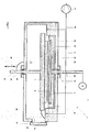
- Fig. 1 shows a simplified representation of a reactor 1 for the treatment of flat substrates 3.
- the reactor 1 may be designed for example as a PECVD reactor.
- the reactor 1 comprises a process space 9 with an electrode 5 and a counter electrode 7, which are designed to produce a plasma for the treatment of a surface to be treated of one or more flat substrates 3.
- the electrodes 5, 7 can be connected to or connected to a voltage source (not shown in detail), preferably a high-frequency supply source, in the process space 9 in order to generate an electric field.
- the electrodes 5, 7 are preferably designed for treating substrates having an area of at least 1.4 m 2 as a treatment or processing step in the production of highly efficient thin-film solar modules, for example of amorphous or microcrystalline silicon thin-film solar cells.
- the electrodes 5, 7 form two opposite walls of the process space 9.
- the process space 9 is located in a vacuum chamber 11, which has a loading and unloading opening 49, which can be closed with a closure device 27.
- the closure device is optional.
- the vacuum chamber 11 is formed by a housing 13 of the reactor 1. To seal against the environment seals 15 are provided.
- the vacuum chamber 11 may have any spatial form, for example, with a round or polygonal, in particular rectangular cross-section.
- the process space 9 is designed, for example, as a flat parallelepiped.
- gaseous material is, in particular, coating or cleaning material.
- cleaning material may be, for example, NF3.
- a vacuum pump 17 and associated vacuum lines 18 are shown.
- a coating material source 19 with a channel 23 is provided, which are connected to a gas distributor 25.
- the gas distributor 25 is formed in the present embodiment, similar to a shower and includes a plurality of opening into the process chamber 9 breakthroughs is introduced by the gaseous material in the process chamber 9. It will be understood that the means for introducing gaseous material are also different from those shown in FIG. 1 may be formed, as well as the gas distributor 25th
- the reactor 1 has a device for varying the relative distance between the electrodes, which in the embodiment of the Fig. 1 to 3 as a sliding bolt 41 by means of a bearing plate 43 to perform a linear movement in the vacuum chamber 11 is formed.
- the sliding bolt is connected to the back of the counter electrode 7 facing away from the electrode 5.
- a the pin 41 associated drive is not shown.
- the electrode 5 is arranged in a holding structure in the vacuum chamber 11, the representation Fig. 1 to 3 is formed by the housing rear wall 33.
- the electrode 5 is accommodated in a recess of the holding structure and separated from the vacuum chamber wall by a dielectric 34.
- the substrate 3 is received by the counter electrode 7 on its front side facing the electrode 5.
- the counter electrode 7 covers the recess during the performance of the treatment.
- a gap is formed between an edge region of the counter electrode 7 and an edge region of the recess, which has a width of the order of 1 mm.
- the gap width is dimensioned such that a plasma can be kept in the interior of the process chamber during the execution of the treatment.
- the gap causes between the process chamber and the rest of the interior of the vacuum chamber 11 is not built up a very large pressure gradient.
- Fig. 2 and 3 show a further reactor 1, analogous to in Fig. 1 Reactor 1 shown below. In the following, only the differences are discussed.
- the reactor 1 according to Fig. 2 and 3 has a, preferably circumferential pumping channel 29 which is formed by a groove-shaped second recess in the support structure. Upstream, the pumping channel 29 is connected via Abpumpkanäle 31 with the process chamber 9. The pumping channel 29 is further connected downstream to the vacuum pump 17 via vacuum lines 18. Opposite the vacuum chamber 11, the pumping channel is at a cover of the recesses through the Counter electrode 7 gas-tight separated or separable. For this purpose, preferably temperature-resistant seals 37 are provided. Covering is preferably done while performing the treatment of the flat substrate. This advantageously allows a relatively high working pressure of up to 10 mbar in the process chamber 9 in relation to a working pressure of 10 -2 to 10 -4 mbar in the process chamber during execution of the treatment.
- the counter electrode 7 in the one Fig. 1 to 3 not shown apparatus for receiving flat substrates which is formed such that the or the substrates at least while performing the treatment of the treated or treated surface oriented downward with an angle alpha in a range between 0 ° and 90 ° relative to Lotcardi are arranged.
- a value of the angle alpha of 1, 3, 5, 7, 9, 11, 13, 15, 17, 20, 25, 30, 40, 45 is preferred.
- Fig. 3 If no closure device 27 is shown, the substrate 3 is partially introduced through the opening 49 into the process chamber 9 of the reactor 1.
- a double arrow 47 indicates the loading or Endladeziscardi of the substrate 3 at. It can be seen that the substrate 3 can be introduced into the process space 9 in a particularly simple manner due to the retracted counterelectrode, which is located close to the housing wall 45 of the housing 13, since almost the entire spatial extent of the vacuum chamber 11 is available for this purpose.
- the substrate 3 After introduction of the substrate 3 into the reactor 1, the substrate 3 can be received by the counter electrode 7 on its front side facing the electrode 5.
- the device for receiving substrates may be designed for substrates which are provided with a carrier.
- the device is designed for receiving substrates for frameless recording of one or more substrates or for frameless carriers.
- the device for receiving substrates may also be designed to change the distance between the substrate to be picked up or picked up and the surface of the front side of the counterelectrode.
- the substrate during loading or unloading of the process space a greater distance from said surface of the counter electrode than when performing a treatment.
- the device for receiving substrates may have at least one upper holding element for one or more substrates and at least in a lower region of at least the counter-electrode 7 at least one lower holding element for one or more substrates, at least in an upper edge region of the counter-electrode.
- Fig. 4 is a longitudinal section of a counter electrode 100 and a housing wall 120 of a reactor according to the invention in side view with a vertical direction L shown with a substrate 105 which is oriented with the surface to be treated down at an angle alpha in a range between 0 ° and 90 ° relative to the direction of solder is arranged.
- an electrode which is arranged opposite to the counter electrode.
- the lower holding element is designed as a support element 115 for the lower edge of a substrate 105.
- the support element 115 is in this case as a bolt 118 with a metallic support member 116 which in the in Fig. 4 not shown process space protrudes formed with a preferably made of a ceramic intermediate piece 117, wherein the bolt extends through a passage in the counter electrode 100 in a region of the vacuum chamber 11 on the back of the counter electrode 120.
- the end region of the bolt 118 can press against a stop 119 and thus be moved from the front-side surface of the counter-electrode 100 in the direction of the process space.
- the substrate 105 is moved with its lower edge away from the front surface of the counter electrode 120 and therefore occupies a greater distance from said surface.
- At least parts of the bolt 118 are surrounded by a protective sheath 130 which can be filled with an inert gas, for example a nitrogen, and increase the corrosion protection in this area, which is indicated in particular when introducing highly corrosive cleaning agents
- the upper holding element is designed as an abutment 110 with a metallic abutment part 111 for an upper edge region of the substrate 105.
- the anvil is connected to a bolt 113, which extends through a passage in the counter electrode 100 in a region of the vacuum chamber 11 on the back of the counter electrode 100 itself. Further, an intermediate piece 112, preferably made of a ceramic, is provided between the counterpart part 111 and the bolt 113.
- the holding members which are linearly movable relative to the surface of the front of the counter electrode, are pressed against one or more stops, for example, in one coating-free edge region of a recess in which the electrode is arranged are located.
- the distance between the substrate and the surface of the front side of the counter electrode is reduced, advantageously, the substrate is pressed against the said surface, so that a fixing of the position of the substrate during the execution of the treatment can be achieved.
- one or more holding elements are alternatively or additionally associated with one or both side regions of the substrate.
- the holding members may be pivotally movable relative to the surface of the front of the counter electrode, thereby facilitating a loading or unloading movement of the substrate.
- the holding elements are designed to be electrically floating.
- the Greifarmmodul is designed such that the substrates during loading and unloading, for example, a process space with a treated or a treating surface oriented down with an angle alpha in a range between 0 ° and 90 ° are arranged opposite to the vertical direction.
- the angle alpha preferably has a value of 1 °, 3 °, 5 °, 7 °, 9 °, 11 °, 13 °, 15 °, 17 °, 20 °. 25 °, 30 °, 40 °, 45 °.
- a gripping arm 200 which comprises a frame 205 with an upper and a lower fork prongs 206, 207.
- An abutment 211 is provided on the upper fork prong 206 and supports 212 and 213 are provided on the lower fork prong 207 for a substrate 220 held by the gripper arm 200.
- the gripping arm 200 allows a frameless mounting of the substrate 220, which is arranged standing on one of its lower edges.
- the frame can vertically parallel to the arrow 225 and horizontally parallel to the arrow 230 through Drives are moved. By means of the vertical movement, the substrate 22U can be placed on or received by at least one lower holding element of a holder for substrates.
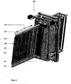
- FIG. 6 is a perspective handler assembly 300 with a frame 305 and a shaft 350 shown.
- the frame is retractable and extendable into the well 350 parallel to the direction of the arrow 330.
- the handler assembly 300 has a second well 355 with another hidden frame.
- a substrate 320 is analogous to the representation in FIG FIG. 5 arranged in the region between the fork prong 306 and the fork tine 307.
- the handler has a Schukompomente 325 for temperature control of substrates at least in the shaft 350 retracted frame 305.
- the handler assembly further includes wheels 340, which ensure their mobility. In addition to a movement of the frame 305 parallel to the direction of the arrow 330, a vertical movement of the frame 305 is possible. The necessary for carrying out the movement of the frame drive units are in the Figures 5 and 6 not shown.
- a handling device is assigned to a reactor according to the invention.
- a loading or unloading of the process space of the reactor takes place by a combination of a movement of the gripper arm parallel to the surface of the substrate to be introduced or removed in the process space in the horizontal or vertical direction.
- the distance between the substrate and the surface of the front of the counter electrode kept relatively large and the substrate deposited on at least one lower support member of the device for receiving substrates or received by the lower support member.
- a replacement of a substrate treated in a reactor by a second substrate can be carried out in a simple manner.
- a first substrate is unloaded from the reactor, introduced into the handling device and then introduced into the reactor already present in the handling device second substrate.
- only a movement of the handling device relative to the reactor is required in order to ensure a correct positioning of the gripper arm with respect to the loading and unloading opening.
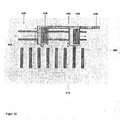
- FIG. 7 An inventive device for processing flat substrates is in Fig. 7 shown in a sectional view in plan view.
- the Fig. 7 1 shows a processing line 400 with a transport space formed as a tunnel 420 with a series of process receptacles configured as reactors 410 for the treatment of flat substrates which are connected to the tunnel 420.
- the tunnel 420 which is preferably tempered, there is a robot 430 which, for clarity, is also shown at a second position in the tunnel 420, designated there by the reference numeral 430 '.
- the robot 430 is arranged on a guide rail 435.
- two heating modules 450 and 455 are provided at the entrance of the processing line, wherein the heating module 450, for example, allows heating at atmospheric pressure.
- the process receptacles or reactors 410 are connected to the tunnel by valves 440.
- the tunnel 420 can be evacuated and / or filled with an inert gas, for example nitrogen or argon or the like.
- Denoted at 415 is a reactor separated from the tunnel.
- a processing line like in Fig. 7 is particularly suitable for processing substrates for thin-film solar cells.
- a thin film solar cell of this type consists of P-i-n layers of amorphous silicon and PIN layers of microcrystalline silicon.
- the doping layers and the intrinsic layers are deposited in different process receptacles to prevent carryover of dopants, which could adversely affect the efficiency of the intrinsic layers.
- the illustrated processing line enables highly effective parallel processing.
- Fig. 8 is a spatial representation of the processing line of Fig. 7 wherein it can be seen that the reactors 410 formed as connectable and detachable modules are movably arranged on rails 416 in order to minimize a standstill of the processing line. During maintenance or in case of failure, the reactors can be disconnected from the tunnel without interrupting the remaining processes.
- a disconnected reactor 415 state is illustrated in greater detail.
- the valve 440 is opened, so that a substrate 490, which is located in the tunnel on a robot can be seen.
- FIG. 10 an embodiment of a device for processing flat substrates is shown, in which the transport robot is designed as a shuttle 438 or 438 'with a vacuum recipient and a flat-surface handling device arranged therein.
- the shuttle has a valve 436 with which it can be vacuum-connected to the process recipient 410.
- the transport space is preferably not evacuated educated.
- a drag chain 439 may be provided to connect the shuttle 438 with power and media supplies.
- the shuttle 438 has its own preferably smaller pumping station, which is arranged with the vacuum recipient, for example, on a baseplate.
- sensors are provided, to determine the relative position of the handler disposed in the vacuum recipient and / or substrates associated therewith in relation to the electrode or counterelectrode in a process recipient.
- a controller can then be used to control a correct coupling for the loading and unloading of the process recipient with a substrate.
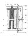
- FIG. 11 is a sectional view in plan view of another reactor for the treatment of flat substrates, with a first vacuum chamber 520, in which a first process space 530 is arranged; with a first electrode 501 and a first counterelectrode 502 for generating a plasma for the treatment of a surface to be treated, wherein the first electrode 501 and the first counterelectrode 502 form two opposite walls of the process space 520.
- a device for varying the relative distance between the electrodes is provided, wherein a first relatively large distance is provided during loading or unloading of the process space 520 with a substrate and a second relatively small distance when performing the treatment of the at least one substrate.
- the device for varying the relative distance between the electrodes comprises eccentric 512 via the rotary drives 508 can cause a parallel displacement of the counter electrode 502.
- disc springs 506 are provided, which allow a wobbling movement of the counter electrode 502, wherein the wobbling movement is limited by the Exenterantriebe 512.
- a counter electrode associated device for receiving substrates is provided, which is analogous to the device already shown, in Fig. 11 but not shown in detail.
- the reactor 500 further comprises a second vacuum chamber in which a second process space is arranged, wherein a second electrode and a second counter electrode are provided for generating a plasma for treating a surface to be treated, each two form opposite walls of the second process space.
- the second vacuum chamber with the second process chamber is analogous to the first vacuum chamber formed with the first process chamber and arranged on the back of the first electrode, ie on the opposite side of the first counter electrode of the first electrode.
- the second vacuum chamber is formed in mirror image to the first.
- the second vacuum chamber further includes means for varying the distance between the electrode and the counter electrode.
- the reactor 500 comprises a high-frequency feeder 510, a housing band 511, a ceramic stop 513, a housing door 514, as well as seals 516 and a vacuum tallow 517.
Description
- Die Erfindung betrifft einen Reaktor und ein Verfahren zur Behandlung von flachen Substraten gemäß den unabhängigen Patentansprüchen.
- Aus der
EP 0312447 B1 ist bereits ein Verfahren zur Herstellung von dünnen Schichten auf Substraten für elektronische oder optoelektronische Verwendung des eines Plasma-Ablagerungsprozesses bekannt (PECVD), wobei in Gegenwart eines Ablagerungsplasmas Reaktionsgase zur Herstellung der Schichten in eine Plasmabox eingeführt werden, die in einer Vakuumkammer angeordnet ist. Dabei wird in der Vakuumkammer ein Druck erzeugt und aufrechterhalten, der niedriger ist als derjenige der in der Plasmabox herrscht. Ähnliche Verfahren sind auch aus derEP 02218112 B1 US 4,798,739 bekannt. Weitere Reaktoren, insbesondere mit mehreren Kammern zur Behandlung eines Substrats werden in derDE 19901426 A1 ,US 6,183,564 B1 ,US 5,944,857 sowie in der japanischen PatentzusammenfassungJP 06267808 A - Das erwähnte zur kostengünstigen Herstellung von Solarzellen mit einem hohen Wirkungsgrad eingesetzte PECVD-Verfahren, bei dem als Prozessgase Silan und Wasserstoff verwendet werden, weißt als wichtige Depositionsparameter den Gasdruck, den Gasfluss, die Leistungsdichte und Frequenz der Plasmaanregung, die Substrattemperatur, die Gaszusammensetzung sowie den Abstand zwischen Elektrode und Gegenelektrode auf. Zur Erreichung von hohen Dispositionsraten sind dabei hohe Gasflüsse und eine Reduzierung des Elektrodenabstandes von Bedeutung. Günstige Abstände zwischen den Elektroden liegen dabei in Bereichen zwischen 0,5 und 15 mm. Bei derart geringen Abständen stellt die Einbringung der Substrate in den Raum zwischen den Elektroden ein Problem dar, wobei zu berücksichtigen Ist, dass zur Gewährleistung einer hohen Produktivität mit einem unterbrechungsfreien Schichtwachstum bei der Beschichtung eine Parallelprozessierung notwendig ist, zu deren Realisierung Cluster-Anlagen eingesetzt werden, die bei den heute gewünschten Substratgrößen von 1,4m2 und mehr einen hohen konstruktiven Aufwand erfordern.
- Bereits bekannt sind Zentral-Cluster bei denen parallel prozessierende Kammern um einen Mittelpunkt herum angeordnet sind, in dem eine zentrale Handlingvorrichtung sitzt. Nachteilig bei Zentral-Cluster-Systemen ist, dass bei großen Substraten die zentrale Handlingvorrichtung sehr groß und schwer zugänglich wird und dass die Anzahl der Prozesskammem und damit der erreichbare Durchsatz begrenzt sind. Bekannt sind ferner Vertikal-Cluster-Anlagen, die beispielsweise in der Herstellung von TFT-Displays eingesetzt werden. Vertikal-Cluster-Systeme beinhalten eine turmartige Architektur mit flachen Prozesskammern, wodurch eine effektive Gastrennung zwischen den Komponenten schwierig und die Anzahl von aufeinander aufgebauten Schichten begrenzt wird.
- Die
DE 101 03 341 A1 beschreibt beispielsweise eine Plasmabehandlungsvorrichtung mit einer Vakuumkammer, in der eine obere Elektrode und eine untere Elektrode angeordnet sind. Weiter gehören dazu eine Hochfrequenzversorgungseinheit zum Anlegen einer Hochfrequenzspannung, eine Abstandjustiereinrichtung zum Justieren des Abstands zwischen den zwei Elektroden, und eine Werkstücktransporteinrichtung zur Be- und Entladung eines Raumbereichs zwischen den zwei Elektroden. Die Verwendung der Plasmabehandlungsvorrichtung erlaubt eine Verringerung eines Abstands zwischen den zwei Elektroden und eine Erhöhung einer Ätzrate. Ferner kann das Werkstück in einfacher Weise zu und von dem Raumbereich zwischen den zwei Elektroden durch Erweitern des Abstands zu- und abgeführt werden. - In der
US 6,818,560 B1 werden eine Plasmabehandlungsvorrichtung sowie ein Verfahren zur Plasmabehandlung beschrieben, die es ermöglichen, das Auftreten einer unerwünschten Entladung bei der Werkstückbearbeitung zu verhindern, ohne das Design zu ändern bzw. ohne den vorgesehenen Durchsatz zu verringern. -
US 2004/102025 A1 beschreibt ein Plasmabearbeitungsverfahren, bei dem das Plasma-Trennen, das Entfernen einer Maske und das Entfernen von Mikro-Rissen durch Ausführen von Plasmabearbeitung an einem Halbleiter-Wafer ausgeführt werden. - Die
US 2006/096857 A1 betrifft eine physikalische Gasphasenabscheidungskammer (PVD) mit einer drehbaren Vorrichtung zur Aufnahme von Substraten, die dem gleichmäßigen Auftragen von dünnen Beschichtungen auf ein Zielobjekt dient. Die Orientierung des Zielobjektes kann, bezogen auf die Substrataufnahmevorrichtung, vertikal oder in einem bestimmten Winkel (etwa 0° bis 45°) relativ zur Drehachse der Substrataufnahmevorrichtung eingestellt werden. - Aufgabe der vorliegenden Erfindung ist es eine effiziente Plasma - Behandlung von flachen Substraten zu ermöglichen, insbesondere einen entsprechenden Reaktor sowie ein Verfahren zur Behandlung von flachen Substraten bereitzustellen, ferner ein einfaches und sicheres Handling flacher Substrate sowie eine verbesserte Herstellung von behandelten Substraten zu ermöglichen.
- Die Aufgabe wird mit den Merkmalen der unabhängigen Patentansprüche gelöst.
- Der erfindungsgemäße Reaktor zur Behandlung von flachen Substraten mit einer Vakuumkammer, in der ein Prozessraum angeordnet ist, wobei eine erste Elektrode und eine Gegenelektrode zur Erzeugung eines Plasmas zur Behandlung einer zu behandelnden Oberfläche verhanden sind und zwei gegenüberliegende Wände des Prozessraums bilden und Mitteln zum Einbringen und Mitteln zur Entfernung von gasförmigen Material, insbesondere Beschichtungs- oder Reinigungsmaterial in den und/oder aus dem Prozessraum, wobei das zumindest eine Substrat durch die Gegenelektrode auf ihrer der Elektrode zugewandten Vorderseite aufnehmbar ist und einer Be- und Entladungsöffnung der Vakuumkammer, vorzugsweise mit einer Verschlussvorrichtung, zeichnet sich dadurch aus, dass eine Vorrichtung zum Variieren des relativen Abstandes zwischen den Elektroden vorgesehen ist, wobei ein erster relativ großer Abstand bei einer Be- oder Entladung der Prozesskammer mit dem zumindest einen Substrat und eine zweiter relativ geringer Abstand bei Durchführung der Behandlung des zumindest einen Substrats verhanden ist. Als flache Substrate werden im Rahmen der Erfindung insbesondere Substrate für Solarzellen, Glasscheiben oder dergleichen bezeichnet. Typisch sind rechteckige Substrate von 1,4 m2 und mehr. Als Behandlung wird im Rahmen der Erfindung jede Art von Modifizierung eines Substrats mittels eines zwischen zwei flachen Elektroden erzeugten Plasma bezeichnet, insbesondere jedoch ein PECVD - Verfahren.
- Vorteilhaft können Elektrode und Gegenelektrode mittels der Vorrichtung zum Variieren des Abstandes vergleichsweise dicht aneinander herangeführt werden, wobei sich auch der Abstand
- Der erfindungsgemäße Reaktor ist dadurch gekennzeichnet, dass eine Haltestruktur (33) in der Vakuumkammer (11) für die Elektrode (5) verhanden und die Elektrode (5) in einer Ausnehmung der Haltestruktur (33) angeordnet ist, dass die Gegenelektrode (7) während der Durchführung der Behandlung die Ausnehmung abdeckt, wobei zwischen einem Randbereich der Gegenelektrode (7) und einem Randbereich der Ausnehmung ein Spalt gebildet ist, der derart dimensioniert ist, dass ein im Prozessraum (9) erzeugtes Plasma innerhalb des Prozessraums (9) gehalten wird oder haltbar ist. zwischen der Elektrode und dem Substrat verringert. Vorteilhaft kann dadurch bei einer Beschichtung der Schichtaufbau positiv beeinflusst werden. Es ist denkbar, auch während der Behandlung des Substrats den Abstand und damit die Prozessparameter zu variieren, um den Behandlungsvorgang zu kontrollieren. Es versteht sich, dass bei einem Variieren des Abstandes sowohl die Elektrode als auch die Gegenelektrode oder auch beide bewegt werden können.
- Der Reaktor ist dadurch ausgezeichnet, daß zumindest eine der Elektroden einen Gasverteiler für Beschichtungsmaterial und/oder Reinigungsmaterial aufweist.
- Ferner kann vorteilhaft während der Durchführung der Behandlung das Substrat mit der zu behandelnden Oberfläche nach unten mit einem Winkel Alpha in einem Bereich zwischen 0 ° und 45 ° gegenüber der Lotrichtung angeordnet sein. Damit wird die Gefahr einer Partikelkontaminierung der empfindlichen zu behandelnden oder behandelten Oberfläche des Substrats reduziert, da weniger Partikel auf diese Oberfläche gelangen können. Derartige Partikel entstehen, wenn im Prozessraum gebildete Schichten, beispielsweise aus Silizium abplatzen. Bevorzugt sind Werte des Winkel Alphas von 1°, 3°, 5°, 7°, 9°, 11°, 13°, 15°, 17°, 20°, 25°, 30°, 40°, 45°, da hiermit der horizontale Platzbedarf durch den Reaktor reduziert wird.
- Gemäß einem weiteren Aspekt der Erfindung wird ein Verfahren zur Behandlung von flachen Substraten in einem Reaktor zur Verfügung gestellt mit einer Vakuumkammer, in der ein Prozessraum angeordnet ist, wobei eine erste Elektrode und eine Gegenelektrode zur Erzeugung eines Plasmas zur Behandlung einer zu behandelnden Oberfläche vorgesehen sind und zwei gegenüberliegende Wände des Prozessraums bilden und Mitteln zum Einbringen und Mitteln zur Entfernung von gasförmigen Material, insbesondere Beschichtungs-oder Reinigungsmaterial in den oder aus dem Prozessraum, wobei der relative Abstand zwischen den Elektroden einstellbar ist und ein erster relativ großer Abstand bei einer Be- oder Entladung der Prozeßkammer mit dem zumindest einen Substrat und eine zweiter relativ geringer Abstand bei Durchführung der Beschichtung des zumindest einen Substrats vorgesehen ist, dadurch gekennzeichnet, dass eine Haltestruktur (33) in der Vakuumkammer (11) für die Elektrode (5) vorgesehen und die Elektrode (5) in einer Ausnehmung der Haltestruktur (33) angeordnet wird, dass die Gegenelektrode (7) während der Durchführung der Behandlung die Ausnehmung abdeckt, wobei zwischen einem Randbereich der Gegenelektrode (7) und einem Randbereich der Ausnehmung ein Spalt gebildet wird, der derart dimensioniert ist dass ein im Prozessraum (9) erzeugtes Plasma innerhalb des Prozessraums (9) gehalten wird oder haltbar ist.
- Weitere vorteilhalte Ausführungsformen der Erfindung in ihren verschiedenen Aspekten sind den abhängigen Ansprüchen zu entnehmen.
- Nachfolgend wir die Erfindung anhand von Zeichnungen näher beschrieben, auf denen sich auch unabhängig von der Zusammenfassung in den Patentansprüchen weitere Merkmale, Einzelheiten und Vorteile der Erfindung ergeben.
- Es zeigen in schematischer Darstellung:
-
Fig. 1 einen Längsschnitt eines Reaktors mit zwei Elektroden in Draufsicht, wobei sich die Elektroden in einem verringerten Abstand zueinander befinden; -
Fig. 2 einen Längsschnitt eines Reaktors analog der Darstellung inFig. 1 , jedoch zusätzlich mit einem Pumpenkanal; -
Fig. 3 die Ansicht des inFig. 2 gezeigten Reaktors, wobei die Elektroden sich in einem vergrößerten Abstand zueinander befinden und ein Substrat teilweise in den Reaktor eingebracht ist. - -
Fig. 4 einen Längsschnitt einer Gegenelektrode und einer Gehäuserand eines Reaktors in Seitenansicht mit einer Lotrichtung L; - -
Fig. 5 einen Greifarm eines Handlervorrichtung für flache Substrate in seitlicher Draufsicht; -
Fig. 6 eine räumliche Darstellung einer Handlerbaugruppe mit einem Rahmengestellt und zwei Schächte; -
Fig. 7 einen Schnitt einer Bearbeitungslinie in Draufsicht; -
Fig. 8 eine räumliche Darstellung einer Bearbeitungslinie; -
Fig. 9 eine räumliche Darstellung von Einzelheiten einer Bearbeitungslinie; -
Fig. 10 einen Schnitt einer Bearbeitungslinie mit einem Shuttle; -
Fig. 11 einen Längsschnitt eines Doppelprozessorraum-Reaktors in Draufsicht; - Die folgende Darstellung von Reaktoren, Handling, Vorrichtungen und Verfahren zur Bearbeitung von flachen Substraten focussieren auf konstruktive Aspekte, wobei es sich für den Fachmann versteht, dass diese Vorrichtungen und Verfahren mit im Einzelnen nicht dargestellten Sensoren, Heiz - und Kühlaggregate, Steuereinrichtungen und Antrieben versehen sind.
-
Fig. 1 zeigt in vereinfachter Darstellung einen Reaktor 1 zur Behandlung von flachen Substraten 3. Der Reaktor 1 kann beispielsweise als PECVD - Reaktor ausgelegt sein. Der Reaktor 1 umfasst einen Prozessraum 9 mit einer Elektrode 5 sowie einer Gegenelektrode 7, die zur Erzeugung eines Plasmas zur Behandlung einer zu behandelnden Oberfläche eines oder mehrerer flacher Substrate 3 ausgelegt sind. Die Elektroden 5, 7 können zur Erzeugung eines elektrischen Feldes in dem Prozessraum 9 an eine nicht näher dargestellte Spannungsquelle, vorzugsweise eine Hochfrequenz - Versorgungsquelle angeschlossen werden oder angeschlossen sein. Die Elektroden 5,7 sind vorzugsweise ausgelegt zur Behandlung von Substraten mit einer Fläche von mindestens 1,4 m2 als Behandlungs- oder Bearbeitungsschritt bei der Herstellung von hocheffizienten Dünnschichtsolarmodulen, beispielsweise von amorphen oder mikrokristallinen Silizium - Dünnschicht - Solarzellen. - Die Elektroden 5,7 bilden zwei gegenüberliegende Wände des Prozessraumes 9. Der Prozessraum 9 befindet sich in einer Vakuumkammer 11, die eine Be- und Entladungsöffnung 49 aufweist, welche mit einer Verschlussvorrichtung 27 verschließbar ist. Die Verschlussvorrichtung ist optional. Die Vakuumkammer 11 wird durch ein Gehäuse 13 des Reaktors 1 gebildet. Zur Abdichtung gegenüber der Umwelt sind Dichtungen 15 vorgesehen.
- Die Vakuumkammer 11 kann eine beliebige Raumform, beispielsweise mit einem runden oder mehreckigen, insbesondere rechteckigen Querschnitt aufweisen. Der Prozessraum 9 ist beispielsweise als flaches Parallelepiped ausgebildet.
- Zum Einbringen und zum Entfernen von gasförmigen Material sind an sich bekannte Mittel vorgesehen, wobei es sich bei dem gasförmigen Material insbesondere um Beschichtungs - oder Reinigungsmaterial handelt. Das Reinigungsmaterial kann beispielsweise NF3 sein. Das Einbringen und Entfernen des gasförmigen Materials kann sowohl sequenziell als auch parallel erfolgen.
- In
Fig. 1 bis 2 sind als Mittel zum Entfernen von gasförmigem Material eine Vakuumpumpe 17 und zugeordnete Vakuumleitungen 18 dargestellt. Als Mittel zum Einbringen von gasförmigem Material ist eine Beschichtungsmaterialquelle 19 mit einem Kanal 23 vorgesehen, die an einem Gasverteiler 25 angeschlossen sind. Der Gasverteiler 25 ist in der vorliegenden Ausführungsform ähnlich einer Dusche ausgebildet und umfasst eine Vielzahl von in den Prozessraum 9 mündenden Durchbrüche durch die gasförmiges Material in den Prozessraum 9 eingebracht wird. Es versteht sich, dass die Mittel zum Einbringen von gasförmigem Material auch verschieden von der der Darstellung inFigur 1 ausgebildet sein können, ebenso wie der Gasverteiler 25. - Erfindungsgemäß weißt der Reaktor 1 eine Vorrichtung zum Variieren des relativen Abstandes zwischen den Elektroden auf, welche in der Ausführungsform der
Fig. 1 bis 3 als Schiebebolzen 41 der mittels einer Lagerplatte 43 eine Linearbewegung in der Vakuumkammer 11 ausführen kann ausgebildet ist. Der Schiebebolzen ist mit der Elektrode 5 abgewandten Rückseite der Gegenelektrode 7 verbunden. Ein dem Schiebebolzen 41 zugeordneter Antrieb ist nicht dargestellt. - Die Elektrode 5 ist in einer Haltestruktur in der Vakuumkammer 11 angeordnet, die der Darstellung
Fig. 1 bis 3 von der Gehäuserückwand 33 gebildet ist. Dazu ist die Elektrode 5 in einer Ausnehmung der Haltestruktur untergebracht und von der Vakuumkammerwand durch ein Dielektrikum 34 getrennt. Das Substrat 3 wird durch die Gegenelektrode 7 auf ihrer der Elektrode 5 zugewandten Vorderseite aufgenommen. - In der Darstellung der
Fig. 1 ist ersichtlich, dass die Gegenelektrode 7 während der Durchführung der Behandlung die Ausnehmung abdeckt. Dabei wird zwischen einem Randbereich der Gegenelektrode 7 und einem Randbereich der Ausnehmung ein Spalt gebildet, der eine Breite in der Größenordnung von 1 mm aufweist. Die Spaltbreite ist derart dimensioniert, dass ein Plasma im inneren des Prozessraums während der Durchführung der Behandlung gehalten werden kann. Der Spalt führt dazu, dass zwischen dem Prozessraum und dem übrigen Innenraum der Vakuumkammer 11 kein allzu großes Druckgefälle aufgebaut wird. Durch die Vakuumleitungen 18 sind Bereiche der Vakuumkammer 11, die außerhalb des Prozessraums 9 angeordnet sind, mit der Vakuumpumpe 17 verbunden, so dass bei Betrieb der Vakuumpumpe 17 aufgrund des größeren Volumens auf eine einfache Weise eine hohe Homogenität der Gasflüsse aus dem Prozessraum 9 über den Spalt erreicht werden kann. Es versteht sich, dass auch andere - Konfigurationen der Mittel zum Entfernen zum gasförmigen Material aus den Prozessraum von der Erfindung umfasst werden. -
Fig. 2 und3 zeigen einen weiteren Reaktor 1, analog dem inFig. 1 dargestellten Reaktor 1. Im Folgenden wird lediglich auf die Unterschiede eingegangen. - Der Reaktor 1 gemäß
Fig. 2 und3 weist einen, vorzugsweise umlaufenden Pumpkanal 29 auf, der durcheine nutförmige zweite Ausnehmung in der Haltestruktur gebildet ist. Stromaufwärts ist der Pumpkanal 29 über Abpumpkanäle 31 mit dem Prozessraum 9 verbunden. Der Pumpkanal 29 ist ferner stromabwärts mit der Vakuumpumpe 17 über Vakuumleitungen 18 verbunden. Gegenüber der Vakuumkammer 11 ist der Pumpkanal bei einer Abdeckung der Ausnehmungen durch die Gegenelektrode 7 gasdicht abgetrennt oder abtrennbar. Hierzu sind vorzugsweise temperaturfesten Dichtungen 37 vorgesehen. Eine Abdeckung erfolgt vorzugsweise während der Durchführung der Behandlung des flachen Substrats. Dies ermöglicht vorteilhaft während einer Durchführung der Behandlung einen relativ hohen Arbeitsdruck von bis zu 10 mbar im Prozessraum 9 gegenüber einem Arbeitsdruck 10-2 bis 10-4 mbar in der Prozesskammer. - Erfindungsgemäß ist in einer weiteren Ausführungsform vorgesehen, dass die Gegenelektrode 7 eine in den
Fig. 1 bis 3 nicht dargestellte Vorrichtung zur Aufnahme von flachen Substraten aufweist, die derart ausgebildet ist, dass das oder die Substrate zumindest während der Durchführung der Behandlung der zu behandelnden oder behandelten Oberfläche nach unten orientiert mit einem Winkel Alpha in einem Bereich zwischen 0° und 90° gegenüber der Lotrichtung angeordnet sind. Bei einer derartigen Anordnung eines Substrats können Kontaminationen der zu beschichtenden oder beschichteten Oberfläche des Substrats vermieden oder zumindest reduziert werden, da die betreffenden Partikel im Schwerefeld nach unten und sich damit von der gefährdeten Oberfläche entfernen. Bevorzugt ist ein Wert des Winkels Alpha von 1 °, 3°, 5°, 7°, 9°, 11 °, 13°, 15°, 17°, 20°, 25°, 30°, 40°, 45°. - In
Fig. 3 ist keine Verschlussvorrichtung 27 dargestellt, wobei das Substrat 3 teilweise durch die Öffnung 49 in den Prozessraum 9 des Reaktors 1 eingebracht ist. Ein Doppelpfeil 47 deutet die Belade- bzw. Endladebewegungsrichtung des Substrats 3 an. Es ist zu erkennen, dass durch die zurückgezogene Gegenelektrode, die sich nahe der Gehäusewand 45 des Gehäuses 13 befindet, das Substrat 3 besonders einfach in den Prozessraum 9 eingebracht werden kann, da dazu fast die gesamte räumliche Ausdehnung der Vakuumkammer 11 zur Verfügung steht. - Nach Einbringen des Substrats 3 in den Reaktor 1 kann das Substrat 3 durch die Gegenelektrode 7 auf ihrer der Elektrode 5 zugewandten Vorderseite aufgenommen werden.
- Die Vorrichtung zur Aufnahme von Substraten kann ausgelegt sein für Substrate die mit einem Carrier versehen sind.
- In einer bevorzugten Ausführungsform der Erfindung ist die Vorrichtung zur Aufnahme von Substraten zur rahmenlosen Aufnahme eines oder mehrerer Substrate bzw. für rahmenlose Carrier ausgelegt.
- Die Vorrichtung zur Aufnahme von Substraten kann ferner ausgebildet sein zur Änderung des Abstandes zwischen dem aufzunehmenden oder aufgenommenen Substrat und der Oberfläche der Vorderseite der Gegenelektrode. Insbesondere kann das Substrat bei Be- oder Entladung des Prozessraums einen größeren Abstand von der genannten Oberfläche der Gegenelektrode aufweisen als bei Durchführung einer Behandlung.
- Die Vorrichtung zur Aufnahme von Substraten kann zumindest in einem oberen Randbereich der Gegenelektrode 7 zumindest ein oberes Halteelement für ein oder mehrere Substrate und zumindest in einem unteren Bereich zumindest der Gegenelektrode 7 zumindest ein unteres Halteelement für ein oder mehrere Substrate aufweisen.
- In
Fig. 4 ist ein Längsschnitt einer Gegenelektrode 100 und einer Gehäusewand 120 eines erfindungsgemäßen Reaktors in Seitenansicht mit einer Lotrichtung L dargestellt mit einem Substrat 105, welches mit der zu behandelnden Oberfläche nach unten orientiert mit einem Winkel Alpha in einem Bereich zwischen 0° und 90° gegenüber der Lotrichtung angeordnet ist. Nicht dargestellt ist eine Elektrode, die der Gegenelektrode gegenüber angeordnet ist. - Das untere Halteelement ist als Auflageelement 115 für die untere Kante eines Substrats 105 ausgebildet. Das Auflageelement 115 ist dabei als Bolzen 118 mit einem metallischen Auflageteil 116, der in den in
Fig. 4 nicht dargestellten Prozessraum hereinragt mit einem vorzugsweise aus einer Keramik bestehenden Zwischenstück 117 ausgebildet, wobei der Bolzen durch eine Durchführung in der Gegenelektrode 100 sich in einen Bereich der Vakuumkammer 11 auf der Rückseite der Gegenelektrode 120 erstreckt. Der Endbereich des Bolzens 118 kann bei dem Zurückziehen der Gegenelektrode 100 in Richtung auf die Gehäusewand 120 gegen einen Anschlag 119 drücken und damit aus der vorderseitigen Oberfläche der Gegenelektrode 100 in-Richtung auf den Prozessraum bewegt werden. Damit wird das Substrat 105 mit seiner unteren Kante von der vorderseitigen Oberfläche der Gegenelektrode 120 wegbewegt und nimmt daher einen größeren Abstand zu der genannten Oberfläche ein. Zumindest Teile des Bolzens 118 sind von einer Schutzhülle 130, die mit einem Inertgas, beispielsweise ein Stickstoff gefüllt werden kann, umgeben und erhöht den Korrosionsschutz in diesem Bereich, was insbesondere bei Einbringung von hoch korrosiven Reinigungsmitteln angezeigt ist - Das obere Halteelement ist als Gegenlager 110 mit einem metallischen Gegenlagerteil 111 für einen oberen Randbereich des Substrats 105 ausgebildet. Das Gegenlager ist mit einem Bolzen 113 verbunden, der durch eine Durchführung in der Gegenelektrode 100 in einen Bereich der Vakuumkammer 11 auf der Rückseite der Gegenelektrode 100 sich erstreckt. Ferner ist ein vorzugsweise aus einer Keramik bestehendes Zwischenstück 112 zwischen Gegenlagerteil 111 und dem Bolzen 113 vorgesehen. Der Bolzen 113 kann bei einem Zurückziehen der Gegenelektrode 100 in Richtung auf die Gehäusewand 120 gegen einen Anschlag 114 drücken und dabei eine Bewegung relativ von der vorderseitigen Oberfläche der Gegenelektrode 100 ausführen. Damit kann der Abstand zwischen den Substrat 105 und der vorderseitigen Oberfläche der Gegenelektrode 100 vergrößert werden. Durch die dargestellte Änderung des Abstandes zwischen Substrat 105 und der Oberfläche der Vorderseite der Gegenelektrode 100 wird eine sichere Be- und Entladung des Prozessraumes erreichbar, da das Substrat während Be- und Entladung gegenüber der Oberfläche der Vorderseite der Gegenelektrode 100 räumlich freigestellt ist.
- Bei einer bevorzugten Ausführungsform der Erfindung werden ferner, wenn die Gegenelektrode 100 beispielsweise zur Durchführung der Behandlung eines Substrats in Richtung auf die Elektrode bewegt ist, die relativ zur Oberfläche der Vorderseite der Gegenelektrode linear bewegbaren Halteelemente gegen einen oder mehrere Anschläge gedrückt, die beispielsweise in einem beschichtungsfreien Randbereich einer Ausnehmung in der die Elektrode angeordnet ist, sich befinden. Damit wird der Abstand zwischen Substrat und Oberfläche der Vorderseite der Gegenelektrode verringert, vorteilhafter weise wird das Substrat gegen die genannte Oberfläche gedrückt, so dass eine Fixierung der Position des Substrats während der Durchführung der Behandlung erreicht werden kann. In einer weiteren Ausführungsform der Erfindung sind alternativ oder zusätzlich ein oder mehrere Halteelemente einem oder beiden Seitenbereichen des Substrats zugeordnet.
- Ferner können die Halteelemente relativ zur Oberfläche der Vorderseite der Gegenelektrode schwenkbar bewegbar sein, um damit eine Be- oder Entladungsbewegung des Substrats zu erleichtern.
- Da zumindest während der Behandlung, insbesondere während der Durchführung einer Beschichtung definierte Potentialverhältnisse im Prozessraum wichtig sind, sind die Halteelemente elektrisch floatend ausgebildet.
- Bei einer Handlingvorrichtung für flache Substrate mit zumindest einem Greifarmmodul ist das Greifarmmodul derartig ausgebildet, dass die Substrate während der Be-und Entladung, beispielsweise eines Prozessraums mit einer zu behandelnden oder einer behandelnden Oberfläche nach unten orientiert mit einem Winkel Alpha in einem Bereich zwischen 0° und 90° gegenüber der Lotrichtung angeordnet sind. Der Winkel Alpha weist vorzugsweise einen Wert von 1°, 3°, 5°, 7°, 9°, 11°, 13°, 15°, 17°, 20°. 25°, 30°, 40°, 45° auf.
- In
Figur 5 ist ein Greifarm 200 dargestellt, der ein Rahmengestell 205 mit einer oberen und einer unteren Gabelzinke 206, 207 umfasst. An der oberen Gabelzinke 206 ist ein Gegenlager 211 und an der unteren Gabelzinke 207 sind Auflagen 212 und 213 für ein von dem Greifarm 200 gehaltertes Substrat 220 vorgesehen. Der Greifarm 200 ermöglicht eine rahmenlose Halterung des Substrats 220, wobei dieses auf einer seiner unteren Kanten stehend angeordnet ist. Das Rahmengestell kann vertikal parallel zum Pfeil 225 und horizontal parallel zum Pfeil 230 durch Antriebe bewegt werden. Mittels der Vertikalbewegung kann das Substrat 22U auf zumindest ein unteres Halteelement einer Halterung für Substrate aufgesetzt oder von diesem aufgenommen werden. - In
Figur 6 ist perspektivisch eine Handlerbaugruppe 300 mit einem Rahmengestell 305 und einem Schacht 350 dargestellt. - Das Rahmengestellt ist in den Schacht 350 ein- und ausfahrbar parallel zur Richtung des Pfeils 330. Ferner weist die Handlerbaugruppe 300 einen zweiten Schacht 355 auf mit einem weiteren nicht sichtbaren Rahmengestellt. Ein Substrat 320 ist Analog zu der Darstellung in
Figur 5 im Bereich zwischen der Gabelzinke 306 und der Gabelzinke 307 angeordnet. Ferner weist der Handler eine Heizkompomente 325 zur Temperierung von Substraten zumindest in den Schacht 350 eingefahrenes Rahmengestell 305 auf. Die Handlerbaugruppe weist ferner Räder 340 auf, mit denen ihrer Verfahrbarkeit gewährleistet wird. Neben einer Bewegung des Rahmengestells 305 parallel zur Richtung des Pfeils 330 ist eine Vertikalbewegung des Rahmengestells 305 möglich. Die zur Durchführung der Bewegung des Rahmengestells erforderlichen Antriebsaggregate sind in denFiguren 5 und6 nicht dargestellt. - Bevorzugt ist eine Handlingvorrichtung einem erfindungsgemäßen Reaktor zugeordnet. Dabei erfolgt eine Be- oder Entladung des Prozessraums des Reaktors durch eine Kombination einer Bewegung des Greifarms parallel zur Oberfläche des in den Prozessraum einzubringenden oder zu entfernenden Substrats in horizontaler bzw. vertikaler Richtung. Vorzugsweise wird, wie im Zusammenhang mit
Figur 4 -dargestellt wurde, während einer Be- oder Entladung der Abstand zwischen dem Substrat und der Oberfläche der Vorderseite der Gegenelektrode relativ groß gehalten und das Substrat auf zumindest ein unteres Halteelement der Vorrichtung zur Aufnahme von Substraten abgesetzt oder von dem unterem Halteelement aufgenommen. - Bei einer Handlingvorrichtung mit einem ersten und einem zweiten Greifarm kann auf eine einfache Weise ein Austausch eines in einem Reaktor behandelten Substrats durch ein zweites Substrat erfolgen. Hierbei wird ein erstes Substrat aus dem Reaktor entladen, in die Handlingvorrichtung eingeführt und anschließend ein bereits in der Handlingvorrichtung vorhandenes zweites Substrat in den Reaktor eingeführt. Hierbei ist lediglich eine Bewegung der Handlingvorrichtung relativ zu dem Reaktor erforderlich um eine korrekte Positionierung des Greifarms gegenüber der Be- und Entladungsöffnung zu gewährleisten.
- Eine erfindungsgemässe Vorrichtung zur Bearbeitung von flachen Substraten ist in
Fig. 7 in einer Schnittdarstellung in Draufsicht dargestellt. - Die
Fig. 7 zeigt dabei eine Bearbeitungslinie 400 mit einem als Tunnel 420 ausgebildeten Transportraum mit einer Reihe von als Reaktoren 410 ausgebildeten Prozessrezipienten zur Behandlung von flachen Substraten die mit dem Tunnel 420 verbunden sind. - In dem, vorzugsweise temperierten Tunnel 420 befindet sich ein Roboter 430 der zur Verdeutlichung auch an einer zweiten Position im Tunnel 420, dort mit dem Bezugszeichen 430' bezeichnet, dargestellt ist. Der Roboter 430 ist auf einer Führungsschiene 435 angeordent. Ferner sind beim Eingang der Bearbeitungslinie zwei Heizmodule 450 und 455 vorgesehen, wobei das Heizmodul 450 beispielsweise eine Heizung bei atmosphärischen Druck ermöglicht. Die Prozessrezipienten bzw. Reaktoren 410 sind mit Ventilen 440 mit dem Tunnel verbunden. Der Tunnel 420 ist evakuierbar und/oder mit einem Inertgas, beispielsweise Stickstoff oder Argon oder dergleichen befüllbar. Mit 415 ist ein von dem Tunnel abgetrennter Reaktor bezeichnet.
- Eine Bearbeitungslinie wie in
Fig. 7 ist insbesondere zur Bearbeitung von Substraten für Dünnschichtsolarzellen geeignet. Eine deratige Dünnschichtsolarzelle besteht aus P- i - n - Schichten aus amorphen Silizium und P-I-N-Schichten aus mikrokristallieden Silizium. Vorzugsweise werden die Dotierschichten und die intrinsischen Schichten in unterschiedlichen Prozessrezipienten abgeschieden um eine Verschleppung Dotierstoffen, die die Effizienz der intrinsischen Schichten negativ beeinflussen könnte, zu verhindern. Die dargestellte Bearbeitungslinie ermöglicht ein hocheffektives Parallelprozessieren. - - In
Fig. 8 ist eine räumliche Darstellung der Bearbeitungslinie vonFig. 7 gezeigt, wobei erkennbar ist, daß die als an- und abkoppelbare Module ausgebildeten Reaktoren 410 auf Schienen 416 verfahrbar angeordnet sind, um einen Stillstand der Bearbeitungslinie zu minimieren. Bei Wartung oder im Störungsfall können die Reaktoren vom Tunnel abgekoppelt werden, ohne die verbleibenden Prozesse zu unterbrechen. - In
Fig. 9 ist für eine Bearbeitungslinie 400 ein Zustand mit einem abgekoppelten Reaktor 415 genauer illustriert. Zur Veranschaulichung ist dabei das Ventil 440 geöffnet, so daß ein Substrat 490, welches sich in dem Tunnel auf einem Roboter befindet erkennbar ist. - In
Figur 10 ist eine Ausführungsform einer Vorrichtung zur Bearbeitung von flachen Substraten dargestellt, bei der der Transportroboter als Shuttle 438 bzw. 438' mit einem Vakuumrezipienten und einer in diesen angeordneten Handlingvorrichtung für flache Substrate ausgebildet ist. Der Shuttle weist ein Ventil 436 auf mit dem er mit den Prozessrezipienten 410 Vakuumtechnisch verbunden werden kann. Bei dieser Ausführungsform ist der Transportraum vorzugsweise nicht evakuierbar ausgebildet. Eine derartige Ausführungsform ist insbesondere für sehr große Substrate geeignet, da das zu evakuierende Volumen gering gehalten werden kann. Zur Verbindung des Shuttle 438 mit Leistungs- und Medienversorgungen kann eine Schleppkette 439 vorgesehen sein. In einer Ausführungsform weist der Shuttle 438 einen eigenen vorzugsweise kleineren Pumpstand auf, der mit dem Vakuumrezipienten beispielsweise auf einer Grundplatte angeordnet ist. Bei einer Ankopplung des Shuttle 438 bzw. des Vakuumrezipienten an einen Prozessrezipienten, kann das sich zwischen den beiden Ventilen befindliche Zwischenvolumen über eine eigene Pumpe oder über ein Dosierventil über die gegebenenfalls vorhandene Shuttlepumpe abgepumpt werden. - Vorteilhaft ist, wenn Sensoren vorgesehen sind die Relativposition des im Vakuumrezipienten angeordneten Handlers und/oder diesen zugeordneten Substraten gegenüber der Elektrode oder Gegenelektrode in einem Prozessrezipienten zu ermitteln. Über eine Steuerung kann dann eine korrekte Ankopplung für die Be- und Entladung des Prozessrezipienten mit einem Substrat gesteuert werden.
- In
Fig. 11 ist in einer Schnittdarstellung in Draufsicht ein weiterer Reaktor zur Behandlung von flachen Substraten dargestellt, mit einer ersten Vakuumkammer 520, in der ein erster Prozessraum 530 angeordnet ist; mit einer ersten Elektrode 501 und einer ersten Gegenelektrode 502 zur Erzeugung eines Plasmas zur Behandlung einer zu behandelnden Oberfläche, wobei die erste Elektrode 501 und die erste Gegenelektrode 502 zwei gegenüberliegende Wände des Prozessraumes 520 bilden. - Ferner ist eine Vorrichtung zum Variieren des relativen Abstandes zwischen den Elektroden vorgesehen, wobei ein erster relativ großer Abstand bei einer Be- oder Entladung der Prozessraums 520 mit einem Substrat und ein zweiter relativ geringer Abstand bei Durchführung der Behandlung des zumindest einen Substrats vorgesehen ist.
- Die Vorrichtung zum Variieren des relativen Abstandes zwischen den Elektroden umfast Exenter 512 über die Drehantriebe 508 eine Parallelverschiebung der Gegenelektrode 502 bewirken können. Ferner sind Tellerfedern 506 vorgesehen, die eine Taumelbewegung der Gegenelektrode 502 zulassen, wobei die Taumelbewegung durch die Exenterantriebe 512 begrenzt ist. Ferner ist eine der Gegenelektrode zugeordnete Vorrichtung zur Aufnahme von Substraten vorgesehen, die analog der bereits dargestellten Vorrichtung ist, in
Fig. 11 jedoch nicht in Einzelheiten gezeigt ist. - Der Reaktor 500 umfasst ferner eine zweite Vakuumkammer in der ein zweiter Prozessraum angeordnet ist, wobei eine zweite Elektrode und eine zweite Gegenelektrode zur Erzeugung eines Plasmas zur Behandlung einer zu behandelnden Oberfläche vorgesehen sind, die jeweils zwei gegenüberliegende Wände des zweiten Prozessraumes bilden. Die zweite Vakuumkammer mit dem zweiten Prozessraum ist analog der ersten Vakuumkammer mit dem ersten Prozessraum ausgebildet und auf der Rückseite der ersten Elektrode angeordnet, d.h. auf der der ersten Gegenelektrode gegenüber liegenden Seite der ersten Elektrode. Bevorzugt ist die zweite Vakuumkammer spiegelbildlich zur ersten ausgebildet. Die zweite Vakuumkammer beinhaltet ferner einen Vorrichtung zum Variieren des Abstandes zwischen Elektrode und Gegenelektrode. Ferner umfasst der Reaktor 500 eine Hochfrequenzzuführung 510, ein Gehäuseband 511, einen keramischer Anschlag 513, eine Gehäusetür 514 sowie Dichtungen 516 und einen Vakuumbalg 517.
-
- 1
- Reaktor
- 3
- Substrat
- 5
- erste Elektrode
- 7
- zweite Elektrode
- 9
- Prozessraum
- 11
- Vakuumkammer
- 13
- Gehäuse
- 15
- Dichtung
- 17
- Vakuumpumpe
- 18
- Vakuumleitungen
- 19
- Beschichtungsmaterialquelle
- 21
- Oberfläche
- 23
- Kanal
- 25
- Gasverteiler
- 27
- Verschlussvorrichtung
- 29
- Pumpkanal
- 31
- Abpumpkanäle
- 33
- Gehäuserückwand
- 34
- Dilektrikum
- 35
- Nut
- 37
- Dichtringe
- 38
- Dichtringe
- 39
- Doppelpfeil
- 41
- Schiebebolzen
- 43
- Lagerplatte
- 45
- Gehäusewand
- 47
- Doppelpfeil
- 49
- Öffnung
- 100
- Gegenelektrode
- 105
- Substrat
- 110
- Gegenlager
- 111
- Gegenlagerteil
- 112
- Zwischenstück
- 113
- Bolzen
- 114
- Anschlag
- 115
- Auflageelement
- 116
- Auflagenteil
- 117
- Zwischenstück
- 118
- Bolzen
- 119
- Anschlag
- 120
- Gehäusewand
- 130
- Schutzhülle
- 200
- Greifarm
- 205
- Rahmegestell
- 206
- Gabelzinke
- 207
- Gabelzinke
- 211
- Gegenlager
- 212
- Auflage
- 213
- Auflage
- 220
- Substrat
- 225
- Pfeil
- 230
- Pfeil
- 300
- Handierbaugruppe
- 305
- Rahmengestellt
- 306
- Gabelzinke
- 307
- Gabelzinke
- 320
- Substrat
- 325
- Heizkomponente
- 330
- Pfeil
- 340
- Räder
- 350
- Schacht
- 355
- Schacht
- 400
- Bearbeitungslinie
- 405
- Bearbeitungslinie
- 410
- Reaktoren
- 415
- abgetrennter Reaktor
- 416
- Schienen
- 420
- Tunnel
- 430
- Roboter
- 430'
- Roboter
- 435
- Führungsschiene
- 436
- Ventil
- 439
- Pleppkette
- 440
- Ventil
- 450
- Heizmodul
- 455
- Heizmodul
- 460
- Pfeil
- 470
- Pfeil
- 480
- Pfeil
- 490
- Substrat
- 500
- Reaktor
- 501
- Elektroden
- 502
- Gegenelektrode
- 503
- Dielektrikum
- 504
- Substrat
- 505
- Zu- und Abfuhrleitungen
- 506
- Tellerfedern
- 507
- Flachbandaufhängung
- 508
- Drehantriebe
- 509
- Hochfrequenzkontaktbänder
- 510
- Hochfrequenzzuführung
- 511
- Gehäuseband
- 512
- Excenter
- 513
- keramischer Anschlag
- 514
- Gehäusetür
- 515
- zweite Hälfte des Reaktors
- 516
- Dichtungen
- 517
- Vakuumbalg
Claims (15)
- Reaktor (1) zur Behandlung von flachen Substraten (3), insbesondere zur Beschichtung von flachen Substraten (3) mit einem Beschichtungsmaterial, mit- einer Vakuumkammer (11), in der ein Prozessraum (9) angeordnet ist, wobei eine erste Elektrode (5) und eine Gegenelektrode (7) zur Erzeugung eines Plasmas zur Behandlung einer zu behandelnden Oberfläche vorhanden sind und zwei gegenüberliegende Wände des Prozessraums (9) bilden- Mitteln zum Einbringen und Mitteln zur Entfernung von gasförmigen Material, insbesondere Beschichtungs- und/oder Reinigungsmaterial in den und/oder aus dem Prozessraum (9)- wobei das zumindest eine Substrat (3) durch die Gegenelektrode (7) auf ihrer der Elektrode (5) zugewandten Vorderseite aufnehmbar ist- einer Be-und Entladungsöffnung der Vakuumkammer (11), vorzugsweise mit einer Verschlussvorrichtung (27),wobei eine Vorrichtung zum Variieren des relativen Abstandes zwischen den Elektroden (5; 7) vorhanden ist, wobei ein erster relativ großer Abstand bei einer Be- oder Entladung der Prozesskammer (9) mit dem zumindest einen Substrat und ein zweiter relativ geringer Abstand bei Durchführung der Behandlung des zumindest einen Substrats vorhanden ist
dadurch gekennzeichnet, dass
eine Haltestruktur (33) in der Vakuumkammer (11) für die Elektrode (5) vorgesehen und die Elektrode (5) in einer Ausnehmung der Haltestruktur (33) angeordnet ist, dass die Gegenelektrode (7) während der Durchführung der Behandlung die Ausnehmung abdeckt wobei zwischen einem Randbereich der Gegenelektrode (7) und einem Randbereich der Ausnehmung ein Spalt gebildet ist, der derart dimensioniert ist, dass ein im Prozessraum (9) erzeugtes Plasma innerhalb des Prozessraums (9) gehalten wird oder haltbar ist - Reaktor (1) nach Anspruch 1, dadurch gekennzeichnet, dass zumindest eine der Elektroden einen Gasverteiler für Beschichtungsmaterial und/oder Reinigungsmaterial aufweist.
- Reaktor (1) nach Anspruch 1 oder 2, dadurch gekennzeichnet, dass eine der Gegenelektrode (7) zugeordnete Vorrichtung zur Aufnahme von Substraten (3) vorhanden ist, die derart ausgebildet ist, dass das zumindest eine Substrat (3) zumindest während der Durchführung der Behandlung mit der zu behandelnden Oberfläche nach unten mit einem Winkel Alpha in einem Bereich zwischen 1° und 45° gegenüber der Lotrichtung angeordnet ist
- Reaktor (1) nach einem der vorhergehenden Ansprüche, dadurch gekennzeichnet, dass der Vakuumkammer (11) eine Handlingvorrichtung zur Be- und Entladung des Prozessraums (9) mit zumindest einem Substrat (3) zugeordnet ist, wobei die Handlingvorrichtung derart ausgebildet ist, dass das zumindest eine Substrat (3) zumindest während der Be- und Entladung des Prozessraumes (9) mit der zu behandelnden Oberfläche nach unten mit einem Winkel Alpha in einem Bereich zwischen 0 °und 30° gegenüber der Lotrichtung angeordnet ist
- Reaktor (1) nach einem der Ansprüche 3 bis 4, dadurch gekennzeichnet, dass die Vorrichtung zur Aufnahme von Substraten (3) mit einem Carrierrahmen oder zur rahmenlosen Aufnahme eines oder mehrerer Substrate (3) ausgelegt ist
- Reaktor (1) nach einem der Ansprüche 3 bis 5, dadurch gekennzeichnet, dass die Vorrichtung zur Aufnahme von Substraten zur Änderung des Abstandes zwischen dem Substrat (3) und der Oberfläche der Vorderseite der Gegenelektrode (7) ausgebildet ist
- Reaktor (1) nach einem der Ansprüche 3 bis 6, dadurch gekennzeichnet, dass die Vorrichtung zur Aufnahme von Substraten (3) zumindest in einem oberen Randbereich zumindest ein oberes Halteelement für ein oder mehrere Substrate (3) und zumindest in einem unteren Bereich zumindest ein unteres Halteelement für ein oder mehre Substrate (3) aufweist
- Reaktor (1) nach Anspruch 7, dadurch gekennzeichnet dass das obere Halteelement als Gegenlager für obere Randbereiche eines oder mehrerer Substrate (3) ausgebildet ist
- Reaktor (1) nach Anspruch 7 oder 8. dadurch gekennzeichnet, dass das untere Halteelement als Auflageelement (115) für die untere Kante eines oder mehrerer Substrate (3) ausgebildet ist
- Reaktor (1) nach einem der Ansprüche 7 bis 9, dadurch gekennzeichnet dass das obere und/oder untere Halteelement relativ zur genannten Oberfläche der Gegenelektrode (7) linear und/oder schwenkbar bewegbar ist.
- Reaktor(1) nach einem der einem der Ansprüche 7 bis 10, dadurch gekennzeichnet, dass die Halteelemente ausgebildet sind zur Änderung des Abstandes zwischen dem Substrat (3) und der genannten Oberfläche der Gegenelektrode (7).
- Reaktor (1) nach mindestens einem der Ansprüche 7 bis 11, dadurch gekennzeichnet, dass die Halteelemente elektrisch floatend ausgebildet sind.
- Reaktor (1) nach einem der vorhergehenden Ansprüche, dadurch gekennzeichnet dass die in einer Ausnehmung der Haltestruktur (33) untergebrachte Elektrode (5) von der Vakuumkammerwand durch ein Dielektrikum getrennt ist
- Reaktor (1) nach einem der vorhergehenden Ansprüche, dadurch gekennzeichnet, dass der Reaktor (1) eine Handlingvorrichtung (300) für flache Substrate mit zumindest einem Greifammodul für ein oder mehrere Substrate aufweist, wobei das Greifammodul (200) derart ausgebildet ist, dass die Substrate (3) parallel zu ihrer Oberfläche bewegbar sind und zumindest während der Be- und Entladung eines Prozessraums (9) mit einer zu behandelnden Oberfläche nach unten mit einem Winkel Alpha in einem Bereich zwischen 1° und 45° gegenüber der Lotrichtung angeordnet sind.
- Verfahren zur Behandlung von flachen Substraten (3), insbesondere zur Beschichtung von flachen Substraten mit einem Beschichtungsmaterial in einem Reaktor mit- einer Vakuumkammer (11), in der ein Prozessraum (9) angeordnet ist, wobei eine erste Elektrode (5) und eine Gegenelektrode (7) zur Erzeugung eines Plasmas zur Behandlung einer zu behandelnden Oberfläche vorgesehen sind und zwei gegenüberliegende Wände des Prozessraums (9) bilden- Mitteln zum Einbringen und Mitteln zur Entfernung von gasförmigen Material, insbesondere Beschichtungs- oder Reinigungsmaterial in den oder aus dem Prozessraum (9)- wobei das zumindest eine Substrate (3) von der Gegenelektrode (7) auf ihrer Vorderseite aufnehmbar ist- einer Be- und Entladungsöffnung der Vakuumkammer (11), vorzugsweise mit einer Verschlussvorrichtung (27)wobei der relative Abstand zwischen den Elektroden (5;7) einstellbar ist und ein erster relativ großer Abstand bei einer Be- oder Entladung der Prozesskammer (9) mit dem zumindest einen Substrat (3) und ein zweiter relativ geringer Abstand bei Durchführung der Beschichtung des zumindest einen Substrats (3) vorhanden ist, dadurch gekennzeichnet dass
eine Haltestruktur (33) in der Vakuumkammer (11) für die Elektrode (5) vorhanden und die Elektrode (5) in einer Ausnehmung der Haltestruktur (33) angeordnet wird, dass die Gegenelektrode (7) während der Durchführung der Behandlung die Ausnehmung abdeckt, wobei zwischen einem Randbereich der Gegenelektrode (7) und einem Randbereich der Ausnehmung ein Spalt gebildet wird, der derart dimensioniert ist, dass ein im Prozessraum (9) erzeugtes Plasma innerhalb des Prozessraums (9) gehalten wind oder haltbar ist
Applications Claiming Priority (3)
| Application Number | Priority Date | Filing Date | Title |
|---|---|---|---|
| DE102007022252 | 2007-05-09 | ||
| DE102007022431A DE102007022431A1 (de) | 2007-05-09 | 2007-05-10 | Behandlungssystem für flache Substrate |
| PCT/EP2008/003414 WO2009003552A2 (de) | 2007-05-09 | 2008-04-28 | Behandlungssystem für flache substrate |
Publications (2)
| Publication Number | Publication Date |
|---|---|
| EP2147452A2 EP2147452A2 (de) | 2010-01-27 |
| EP2147452B1 true EP2147452B1 (de) | 2013-04-17 |
Family
ID=39829464
Family Applications (1)
| Application Number | Title | Priority Date | Filing Date |
|---|---|---|---|
| EP08735395.9A Not-in-force EP2147452B1 (de) | 2007-05-09 | 2008-04-28 | Behandlungssystem für flache substrate |
Country Status (15)
| Country | Link |
|---|---|
| US (1) | US20100255196A1 (de) |
| EP (1) | EP2147452B1 (de) |
| JP (1) | JP5243525B2 (de) |
| KR (1) | KR101284961B1 (de) |
| CN (2) | CN103295869A (de) |
| AU (1) | AU2008271675A1 (de) |
| BR (1) | BRPI0811313A2 (de) |
| CA (1) | CA2688522A1 (de) |
| DE (1) | DE102007022431A1 (de) |
| HK (1) | HK1146153A1 (de) |
| MA (1) | MA31423B1 (de) |
| MX (1) | MX2009012112A (de) |
| TN (1) | TN2009000477A1 (de) |
| TW (1) | TW200902755A (de) |
| WO (1) | WO2009003552A2 (de) |
Families Citing this family (249)
| Publication number | Priority date | Publication date | Assignee | Title |
|---|---|---|---|---|
| US9394608B2 (en) | 2009-04-06 | 2016-07-19 | Asm America, Inc. | Semiconductor processing reactor and components thereof |
| JP2013500595A (ja) * | 2009-07-26 | 2013-01-07 | ライボルト オプティクス ゲゼルシャフト ミット ベシュレンクテル ハフツング | プロセスチャンバのクリーニング |
| US8802201B2 (en) | 2009-08-14 | 2014-08-12 | Asm America, Inc. | Systems and methods for thin-film deposition of metal oxides using excited nitrogen-oxygen species |
| MX2012010842A (es) * | 2010-03-22 | 2013-04-03 | Luxxotica Us Holdings Corp | Deposicion auxliada por haz ionico de recubrimientos para lentes oftalmicas. |
| DE102010027168A1 (de) | 2010-07-14 | 2012-01-19 | Leybold Optics Gmbh | Verfahren und Vorrichtung zur Plasmabehandlung flacher Substrate |
| US20130023129A1 (en) | 2011-07-20 | 2013-01-24 | Asm America, Inc. | Pressure transmitter for a semiconductor processing environment |
| CN102888596B (zh) * | 2011-07-22 | 2015-09-02 | 北京北方微电子基地设备工艺研究中心有限责任公司 | 腔室装置及具有该腔室装置的等离子体处理设备 |
| US9017481B1 (en) | 2011-10-28 | 2015-04-28 | Asm America, Inc. | Process feed management for semiconductor substrate processing |
| KR20140033911A (ko) * | 2012-09-11 | 2014-03-19 | 에이에스엠 아이피 홀딩 비.브이. | 증착 장치 및 증착 방법 |
| US10714315B2 (en) | 2012-10-12 | 2020-07-14 | Asm Ip Holdings B.V. | Semiconductor reaction chamber showerhead |
| US20160376700A1 (en) | 2013-02-01 | 2016-12-29 | Asm Ip Holding B.V. | System for treatment of deposition reactor |
| KR101440233B1 (ko) * | 2013-05-27 | 2014-09-12 | 권국래 | 히터블록 위치측정장치 |
| US11015245B2 (en) | 2014-03-19 | 2021-05-25 | Asm Ip Holding B.V. | Gas-phase reactor and system having exhaust plenum and components thereof |
| CN103956315B (zh) * | 2014-05-22 | 2016-05-18 | 中国地质大学(北京) | 一种电极间距可调的等离子体反应腔室及电极间距调整装置 |
| US10858737B2 (en) | 2014-07-28 | 2020-12-08 | Asm Ip Holding B.V. | Showerhead assembly and components thereof |
| US9890456B2 (en) | 2014-08-21 | 2018-02-13 | Asm Ip Holding B.V. | Method and system for in situ formation of gas-phase compounds |
| US10941490B2 (en) | 2014-10-07 | 2021-03-09 | Asm Ip Holding B.V. | Multiple temperature range susceptor, assembly, reactor and system including the susceptor, and methods of using the same |
| JP6354539B2 (ja) * | 2014-11-25 | 2018-07-11 | 東京エレクトロン株式会社 | 基板処理装置、基板処理方法、記憶媒体 |
| US10276355B2 (en) | 2015-03-12 | 2019-04-30 | Asm Ip Holding B.V. | Multi-zone reactor, system including the reactor, and method of using the same |
| DE102015003379A1 (de) | 2015-03-17 | 2016-09-22 | Manz Ag | Plasmaerzeugungsvorrichtung mit einer Induktionsspule |
| US10458018B2 (en) | 2015-06-26 | 2019-10-29 | Asm Ip Holding B.V. | Structures including metal carbide material, devices including the structures, and methods of forming same |
| US10211308B2 (en) | 2015-10-21 | 2019-02-19 | Asm Ip Holding B.V. | NbMC layers |
| US10203604B2 (en) | 2015-11-30 | 2019-02-12 | Applied Materials, Inc. | Method and apparatus for post exposure processing of photoresist wafers |
| US11139308B2 (en) | 2015-12-29 | 2021-10-05 | Asm Ip Holding B.V. | Atomic layer deposition of III-V compounds to form V-NAND devices |
| US10529554B2 (en) | 2016-02-19 | 2020-01-07 | Asm Ip Holding B.V. | Method for forming silicon nitride film selectively on sidewalls or flat surfaces of trenches |
| US10190213B2 (en) | 2016-04-21 | 2019-01-29 | Asm Ip Holding B.V. | Deposition of metal borides |
| US10865475B2 (en) | 2016-04-21 | 2020-12-15 | Asm Ip Holding B.V. | Deposition of metal borides and silicides |
| US10367080B2 (en) | 2016-05-02 | 2019-07-30 | Asm Ip Holding B.V. | Method of forming a germanium oxynitride film |
| US11453943B2 (en) | 2016-05-25 | 2022-09-27 | Asm Ip Holding B.V. | Method for forming carbon-containing silicon/metal oxide or nitride film by ALD using silicon precursor and hydrocarbon precursor |
| US9958782B2 (en) * | 2016-06-29 | 2018-05-01 | Applied Materials, Inc. | Apparatus for post exposure bake |
| US9859151B1 (en) | 2016-07-08 | 2018-01-02 | Asm Ip Holding B.V. | Selective film deposition method to form air gaps |
| US10612137B2 (en) | 2016-07-08 | 2020-04-07 | Asm Ip Holdings B.V. | Organic reactants for atomic layer deposition |
| KR102532607B1 (ko) | 2016-07-28 | 2023-05-15 | 에이에스엠 아이피 홀딩 비.브이. | 기판 가공 장치 및 그 동작 방법 |
| US9812320B1 (en) | 2016-07-28 | 2017-11-07 | Asm Ip Holding B.V. | Method and apparatus for filling a gap |
| US9887082B1 (en) | 2016-07-28 | 2018-02-06 | Asm Ip Holding B.V. | Method and apparatus for filling a gap |
| US10643826B2 (en) | 2016-10-26 | 2020-05-05 | Asm Ip Holdings B.V. | Methods for thermally calibrating reaction chambers |
| US11532757B2 (en) | 2016-10-27 | 2022-12-20 | Asm Ip Holding B.V. | Deposition of charge trapping layers |
| US10714350B2 (en) | 2016-11-01 | 2020-07-14 | ASM IP Holdings, B.V. | Methods for forming a transition metal niobium nitride film on a substrate by atomic layer deposition and related semiconductor device structures |
| US10229833B2 (en) | 2016-11-01 | 2019-03-12 | Asm Ip Holding B.V. | Methods for forming a transition metal nitride film on a substrate by atomic layer deposition and related semiconductor device structures |
| KR102546317B1 (ko) | 2016-11-15 | 2023-06-21 | 에이에스엠 아이피 홀딩 비.브이. | 기체 공급 유닛 및 이를 포함하는 기판 처리 장치 |
| TWI649245B (zh) * | 2016-12-09 | 2019-02-01 | 財團法人金屬工業研究發展中心 | transmission |
| KR20180068582A (ko) | 2016-12-14 | 2018-06-22 | 에이에스엠 아이피 홀딩 비.브이. | 기판 처리 장치 |
| US11581186B2 (en) | 2016-12-15 | 2023-02-14 | Asm Ip Holding B.V. | Sequential infiltration synthesis apparatus |
| US11251019B2 (en) * | 2016-12-15 | 2022-02-15 | Toyota Jidosha Kabushiki Kaisha | Plasma device |
| US11447861B2 (en) | 2016-12-15 | 2022-09-20 | Asm Ip Holding B.V. | Sequential infiltration synthesis apparatus and a method of forming a patterned structure |
| KR20180070971A (ko) * | 2016-12-19 | 2018-06-27 | 에이에스엠 아이피 홀딩 비.브이. | 기판 처리 장치 |
| US10269558B2 (en) | 2016-12-22 | 2019-04-23 | Asm Ip Holding B.V. | Method of forming a structure on a substrate |
| US10867788B2 (en) | 2016-12-28 | 2020-12-15 | Asm Ip Holding B.V. | Method of forming a structure on a substrate |
| US11390950B2 (en) | 2017-01-10 | 2022-07-19 | Asm Ip Holding B.V. | Reactor system and method to reduce residue buildup during a film deposition process |
| US10468261B2 (en) | 2017-02-15 | 2019-11-05 | Asm Ip Holding B.V. | Methods for forming a metallic film on a substrate by cyclical deposition and related semiconductor device structures |
| US10529563B2 (en) | 2017-03-29 | 2020-01-07 | Asm Ip Holdings B.V. | Method for forming doped metal oxide films on a substrate by cyclical deposition and related semiconductor device structures |
| KR102457289B1 (ko) | 2017-04-25 | 2022-10-21 | 에이에스엠 아이피 홀딩 비.브이. | 박막 증착 방법 및 반도체 장치의 제조 방법 |
| US10892156B2 (en) | 2017-05-08 | 2021-01-12 | Asm Ip Holding B.V. | Methods for forming a silicon nitride film on a substrate and related semiconductor device structures |
| US10770286B2 (en) | 2017-05-08 | 2020-09-08 | Asm Ip Holdings B.V. | Methods for selectively forming a silicon nitride film on a substrate and related semiconductor device structures |
| US10886123B2 (en) | 2017-06-02 | 2021-01-05 | Asm Ip Holding B.V. | Methods for forming low temperature semiconductor layers and related semiconductor device structures |
| US11306395B2 (en) | 2017-06-28 | 2022-04-19 | Asm Ip Holding B.V. | Methods for depositing a transition metal nitride film on a substrate by atomic layer deposition and related deposition apparatus |
| KR20190009245A (ko) | 2017-07-18 | 2019-01-28 | 에이에스엠 아이피 홀딩 비.브이. | 반도체 소자 구조물 형성 방법 및 관련된 반도체 소자 구조물 |
| US10541333B2 (en) | 2017-07-19 | 2020-01-21 | Asm Ip Holding B.V. | Method for depositing a group IV semiconductor and related semiconductor device structures |
| US11018002B2 (en) | 2017-07-19 | 2021-05-25 | Asm Ip Holding B.V. | Method for selectively depositing a Group IV semiconductor and related semiconductor device structures |
| US11374112B2 (en) | 2017-07-19 | 2022-06-28 | Asm Ip Holding B.V. | Method for depositing a group IV semiconductor and related semiconductor device structures |
| US10590535B2 (en) | 2017-07-26 | 2020-03-17 | Asm Ip Holdings B.V. | Chemical treatment, deposition and/or infiltration apparatus and method for using the same |
| US10692741B2 (en) | 2017-08-08 | 2020-06-23 | Asm Ip Holdings B.V. | Radiation shield |
| US10770336B2 (en) | 2017-08-08 | 2020-09-08 | Asm Ip Holding B.V. | Substrate lift mechanism and reactor including same |
| US11769682B2 (en) | 2017-08-09 | 2023-09-26 | Asm Ip Holding B.V. | Storage apparatus for storing cassettes for substrates and processing apparatus equipped therewith |
| US11139191B2 (en) | 2017-08-09 | 2021-10-05 | Asm Ip Holding B.V. | Storage apparatus for storing cassettes for substrates and processing apparatus equipped therewith |
| US11830730B2 (en) | 2017-08-29 | 2023-11-28 | Asm Ip Holding B.V. | Layer forming method and apparatus |
| US11056344B2 (en) | 2017-08-30 | 2021-07-06 | Asm Ip Holding B.V. | Layer forming method |
| US11295980B2 (en) | 2017-08-30 | 2022-04-05 | Asm Ip Holding B.V. | Methods for depositing a molybdenum metal film over a dielectric surface of a substrate by a cyclical deposition process and related semiconductor device structures |
| KR102491945B1 (ko) | 2017-08-30 | 2023-01-26 | 에이에스엠 아이피 홀딩 비.브이. | 기판 처리 장치 |
| KR102630301B1 (ko) | 2017-09-21 | 2024-01-29 | 에이에스엠 아이피 홀딩 비.브이. | 침투성 재료의 순차 침투 합성 방법 처리 및 이를 이용하여 형성된 구조물 및 장치 |
| US10844484B2 (en) | 2017-09-22 | 2020-11-24 | Asm Ip Holding B.V. | Apparatus for dispensing a vapor phase reactant to a reaction chamber and related methods |
| JP6863199B2 (ja) | 2017-09-25 | 2021-04-21 | トヨタ自動車株式会社 | プラズマ処理装置 |
| US10658205B2 (en) | 2017-09-28 | 2020-05-19 | Asm Ip Holdings B.V. | Chemical dispensing apparatus and methods for dispensing a chemical to a reaction chamber |
| US10403504B2 (en) | 2017-10-05 | 2019-09-03 | Asm Ip Holding B.V. | Method for selectively depositing a metallic film on a substrate |
| US10923344B2 (en) | 2017-10-30 | 2021-02-16 | Asm Ip Holding B.V. | Methods for forming a semiconductor structure and related semiconductor structures |
| US10910262B2 (en) | 2017-11-16 | 2021-02-02 | Asm Ip Holding B.V. | Method of selectively depositing a capping layer structure on a semiconductor device structure |
| US11022879B2 (en) | 2017-11-24 | 2021-06-01 | Asm Ip Holding B.V. | Method of forming an enhanced unexposed photoresist layer |
| US11639811B2 (en) | 2017-11-27 | 2023-05-02 | Asm Ip Holding B.V. | Apparatus including a clean mini environment |
| JP7214724B2 (ja) | 2017-11-27 | 2023-01-30 | エーエスエム アイピー ホールディング ビー.ブイ. | バッチ炉で利用されるウェハカセットを収納するための収納装置 |
| US10872771B2 (en) | 2018-01-16 | 2020-12-22 | Asm Ip Holding B. V. | Method for depositing a material film on a substrate within a reaction chamber by a cyclical deposition process and related device structures |
| US11482412B2 (en) | 2018-01-19 | 2022-10-25 | Asm Ip Holding B.V. | Method for depositing a gap-fill layer by plasma-assisted deposition |
| TW202325889A (zh) | 2018-01-19 | 2023-07-01 | 荷蘭商Asm 智慧財產控股公司 | 沈積方法 |
| US11018047B2 (en) | 2018-01-25 | 2021-05-25 | Asm Ip Holding B.V. | Hybrid lift pin |
| USD880437S1 (en) | 2018-02-01 | 2020-04-07 | Asm Ip Holding B.V. | Gas supply plate for semiconductor manufacturing apparatus |
| US11081345B2 (en) | 2018-02-06 | 2021-08-03 | Asm Ip Holding B.V. | Method of post-deposition treatment for silicon oxide film |
| CN111699278B (zh) | 2018-02-14 | 2023-05-16 | Asm Ip私人控股有限公司 | 通过循环沉积工艺在衬底上沉积含钌膜的方法 |
| US10896820B2 (en) | 2018-02-14 | 2021-01-19 | Asm Ip Holding B.V. | Method for depositing a ruthenium-containing film on a substrate by a cyclical deposition process |
| KR102636427B1 (ko) | 2018-02-20 | 2024-02-13 | 에이에스엠 아이피 홀딩 비.브이. | 기판 처리 방법 및 장치 |
| US10975470B2 (en) | 2018-02-23 | 2021-04-13 | Asm Ip Holding B.V. | Apparatus for detecting or monitoring for a chemical precursor in a high temperature environment |
| US11473195B2 (en) | 2018-03-01 | 2022-10-18 | Asm Ip Holding B.V. | Semiconductor processing apparatus and a method for processing a substrate |
| US11629406B2 (en) | 2018-03-09 | 2023-04-18 | Asm Ip Holding B.V. | Semiconductor processing apparatus comprising one or more pyrometers for measuring a temperature of a substrate during transfer of the substrate |
| US11114283B2 (en) | 2018-03-16 | 2021-09-07 | Asm Ip Holding B.V. | Reactor, system including the reactor, and methods of manufacturing and using same |
| KR102646467B1 (ko) | 2018-03-27 | 2024-03-11 | 에이에스엠 아이피 홀딩 비.브이. | 기판 상에 전극을 형성하는 방법 및 전극을 포함하는 반도체 소자 구조 |
| US11230766B2 (en) | 2018-03-29 | 2022-01-25 | Asm Ip Holding B.V. | Substrate processing apparatus and method |
| US11088002B2 (en) | 2018-03-29 | 2021-08-10 | Asm Ip Holding B.V. | Substrate rack and a substrate processing system and method |
| KR102501472B1 (ko) | 2018-03-30 | 2023-02-20 | 에이에스엠 아이피 홀딩 비.브이. | 기판 처리 방법 |
| CN108315721B (zh) * | 2018-04-24 | 2020-04-03 | 武汉华星光电技术有限公司 | 成膜机台及成膜制程调整基板偏转量的方法 |
| TW202344708A (zh) | 2018-05-08 | 2023-11-16 | 荷蘭商Asm Ip私人控股有限公司 | 藉由循環沉積製程於基板上沉積氧化物膜之方法及相關裝置結構 |
| TW202349473A (zh) | 2018-05-11 | 2023-12-16 | 荷蘭商Asm Ip私人控股有限公司 | 用於基板上形成摻雜金屬碳化物薄膜之方法及相關半導體元件結構 |
| KR102596988B1 (ko) | 2018-05-28 | 2023-10-31 | 에이에스엠 아이피 홀딩 비.브이. | 기판 처리 방법 및 그에 의해 제조된 장치 |
| US11718913B2 (en) | 2018-06-04 | 2023-08-08 | Asm Ip Holding B.V. | Gas distribution system and reactor system including same |
| US11270899B2 (en) | 2018-06-04 | 2022-03-08 | Asm Ip Holding B.V. | Wafer handling chamber with moisture reduction |
| US11286562B2 (en) | 2018-06-08 | 2022-03-29 | Asm Ip Holding B.V. | Gas-phase chemical reactor and method of using same |
| US10797133B2 (en) | 2018-06-21 | 2020-10-06 | Asm Ip Holding B.V. | Method for depositing a phosphorus doped silicon arsenide film and related semiconductor device structures |
| KR102568797B1 (ko) | 2018-06-21 | 2023-08-21 | 에이에스엠 아이피 홀딩 비.브이. | 기판 처리 시스템 |
| KR20210027265A (ko) | 2018-06-27 | 2021-03-10 | 에이에스엠 아이피 홀딩 비.브이. | 금속 함유 재료를 형성하기 위한 주기적 증착 방법 및 금속 함유 재료를 포함하는 막 및 구조체 |
| CN112292478A (zh) | 2018-06-27 | 2021-01-29 | Asm Ip私人控股有限公司 | 用于形成含金属的材料的循环沉积方法及包含含金属的材料的膜和结构 |
| US10612136B2 (en) | 2018-06-29 | 2020-04-07 | ASM IP Holding, B.V. | Temperature-controlled flange and reactor system including same |
| KR20200002519A (ko) | 2018-06-29 | 2020-01-08 | 에이에스엠 아이피 홀딩 비.브이. | 박막 증착 방법 및 반도체 장치의 제조 방법 |
| US10388513B1 (en) | 2018-07-03 | 2019-08-20 | Asm Ip Holding B.V. | Method for depositing silicon-free carbon-containing film as gap-fill layer by pulse plasma-assisted deposition |
| US10755922B2 (en) | 2018-07-03 | 2020-08-25 | Asm Ip Holding B.V. | Method for depositing silicon-free carbon-containing film as gap-fill layer by pulse plasma-assisted deposition |
| KR102139615B1 (ko) * | 2018-07-10 | 2020-08-12 | 세메스 주식회사 | 기판 처리 장치 |
| US10767789B2 (en) | 2018-07-16 | 2020-09-08 | Asm Ip Holding B.V. | Diaphragm valves, valve components, and methods for forming valve components |
| US11053591B2 (en) | 2018-08-06 | 2021-07-06 | Asm Ip Holding B.V. | Multi-port gas injection system and reactor system including same |
| US10883175B2 (en) | 2018-08-09 | 2021-01-05 | Asm Ip Holding B.V. | Vertical furnace for processing substrates and a liner for use therein |
| US10829852B2 (en) | 2018-08-16 | 2020-11-10 | Asm Ip Holding B.V. | Gas distribution device for a wafer processing apparatus |
| US11430674B2 (en) | 2018-08-22 | 2022-08-30 | Asm Ip Holding B.V. | Sensor array, apparatus for dispensing a vapor phase reactant to a reaction chamber and related methods |
| KR20200030162A (ko) | 2018-09-11 | 2020-03-20 | 에이에스엠 아이피 홀딩 비.브이. | 박막 증착 방법 |
| US11024523B2 (en) | 2018-09-11 | 2021-06-01 | Asm Ip Holding B.V. | Substrate processing apparatus and method |
| US11049751B2 (en) | 2018-09-14 | 2021-06-29 | Asm Ip Holding B.V. | Cassette supply system to store and handle cassettes and processing apparatus equipped therewith |
| CN109346543B (zh) * | 2018-09-29 | 2023-11-17 | 苏州腾晖光伏技术有限公司 | 一种用于光伏组件的层压辅助装置 |
| CN110970344A (zh) | 2018-10-01 | 2020-04-07 | Asm Ip控股有限公司 | 衬底保持设备、包含所述设备的系统及其使用方法 |
| US11232963B2 (en) | 2018-10-03 | 2022-01-25 | Asm Ip Holding B.V. | Substrate processing apparatus and method |
| KR102592699B1 (ko) | 2018-10-08 | 2023-10-23 | 에이에스엠 아이피 홀딩 비.브이. | 기판 지지 유닛 및 이를 포함하는 박막 증착 장치와 기판 처리 장치 |
| KR102546322B1 (ko) | 2018-10-19 | 2023-06-21 | 에이에스엠 아이피 홀딩 비.브이. | 기판 처리 장치 및 기판 처리 방법 |
| KR102605121B1 (ko) | 2018-10-19 | 2023-11-23 | 에이에스엠 아이피 홀딩 비.브이. | 기판 처리 장치 및 기판 처리 방법 |
| USD948463S1 (en) | 2018-10-24 | 2022-04-12 | Asm Ip Holding B.V. | Susceptor for semiconductor substrate supporting apparatus |
| US11087997B2 (en) | 2018-10-31 | 2021-08-10 | Asm Ip Holding B.V. | Substrate processing apparatus for processing substrates |
| KR20200051105A (ko) | 2018-11-02 | 2020-05-13 | 에이에스엠 아이피 홀딩 비.브이. | 기판 지지 유닛 및 이를 포함하는 기판 처리 장치 |
| US11572620B2 (en) | 2018-11-06 | 2023-02-07 | Asm Ip Holding B.V. | Methods for selectively depositing an amorphous silicon film on a substrate |
| US11031242B2 (en) | 2018-11-07 | 2021-06-08 | Asm Ip Holding B.V. | Methods for depositing a boron doped silicon germanium film |
| US10847366B2 (en) | 2018-11-16 | 2020-11-24 | Asm Ip Holding B.V. | Methods for depositing a transition metal chalcogenide film on a substrate by a cyclical deposition process |
| US10818758B2 (en) | 2018-11-16 | 2020-10-27 | Asm Ip Holding B.V. | Methods for forming a metal silicate film on a substrate in a reaction chamber and related semiconductor device structures |
| US11217444B2 (en) | 2018-11-30 | 2022-01-04 | Asm Ip Holding B.V. | Method for forming an ultraviolet radiation responsive metal oxide-containing film |
| KR102636428B1 (ko) | 2018-12-04 | 2024-02-13 | 에이에스엠 아이피 홀딩 비.브이. | 기판 처리 장치를 세정하는 방법 |
| US11158513B2 (en) | 2018-12-13 | 2021-10-26 | Asm Ip Holding B.V. | Methods for forming a rhenium-containing film on a substrate by a cyclical deposition process and related semiconductor device structures |
| TW202037745A (zh) | 2018-12-14 | 2020-10-16 | 荷蘭商Asm Ip私人控股有限公司 | 形成裝置結構之方法、其所形成之結構及施行其之系統 |
| TWI819180B (zh) | 2019-01-17 | 2023-10-21 | 荷蘭商Asm 智慧財產控股公司 | 藉由循環沈積製程於基板上形成含過渡金屬膜之方法 |
| KR20200091543A (ko) | 2019-01-22 | 2020-07-31 | 에이에스엠 아이피 홀딩 비.브이. | 기판 처리 장치 |
| CN111524788B (zh) | 2019-02-01 | 2023-11-24 | Asm Ip私人控股有限公司 | 氧化硅的拓扑选择性膜形成的方法 |
| US11482533B2 (en) | 2019-02-20 | 2022-10-25 | Asm Ip Holding B.V. | Apparatus and methods for plug fill deposition in 3-D NAND applications |
| KR102638425B1 (ko) | 2019-02-20 | 2024-02-21 | 에이에스엠 아이피 홀딩 비.브이. | 기판 표면 내에 형성된 오목부를 충진하기 위한 방법 및 장치 |
| TW202104632A (zh) | 2019-02-20 | 2021-02-01 | 荷蘭商Asm Ip私人控股有限公司 | 用來填充形成於基材表面內之凹部的循環沉積方法及設備 |
| KR102626263B1 (ko) | 2019-02-20 | 2024-01-16 | 에이에스엠 아이피 홀딩 비.브이. | 처리 단계를 포함하는 주기적 증착 방법 및 이를 위한 장치 |
| TW202100794A (zh) | 2019-02-22 | 2021-01-01 | 荷蘭商Asm Ip私人控股有限公司 | 基材處理設備及處理基材之方法 |
| KR20200108242A (ko) | 2019-03-08 | 2020-09-17 | 에이에스엠 아이피 홀딩 비.브이. | 실리콘 질화물 층을 선택적으로 증착하는 방법, 및 선택적으로 증착된 실리콘 질화물 층을 포함하는 구조체 |
| KR20200108243A (ko) | 2019-03-08 | 2020-09-17 | 에이에스엠 아이피 홀딩 비.브이. | SiOC 층을 포함한 구조체 및 이의 형성 방법 |
| KR20200108248A (ko) | 2019-03-08 | 2020-09-17 | 에이에스엠 아이피 홀딩 비.브이. | SiOCN 층을 포함한 구조체 및 이의 형성 방법 |
| JP2020167398A (ja) | 2019-03-28 | 2020-10-08 | エーエスエム・アイピー・ホールディング・ベー・フェー | ドアオープナーおよびドアオープナーが提供される基材処理装置 |
| KR20200116855A (ko) | 2019-04-01 | 2020-10-13 | 에이에스엠 아이피 홀딩 비.브이. | 반도체 소자를 제조하는 방법 |
| KR20200123380A (ko) | 2019-04-19 | 2020-10-29 | 에이에스엠 아이피 홀딩 비.브이. | 층 형성 방법 및 장치 |
| KR20200125453A (ko) | 2019-04-24 | 2020-11-04 | 에이에스엠 아이피 홀딩 비.브이. | 기상 반응기 시스템 및 이를 사용하는 방법 |
| KR20200130121A (ko) | 2019-05-07 | 2020-11-18 | 에이에스엠 아이피 홀딩 비.브이. | 딥 튜브가 있는 화학물질 공급원 용기 |
| KR20200130118A (ko) | 2019-05-07 | 2020-11-18 | 에이에스엠 아이피 홀딩 비.브이. | 비정질 탄소 중합체 막을 개질하는 방법 |
| KR20200130652A (ko) | 2019-05-10 | 2020-11-19 | 에이에스엠 아이피 홀딩 비.브이. | 표면 상에 재료를 증착하는 방법 및 본 방법에 따라 형성된 구조 |
| JP2020188255A (ja) | 2019-05-16 | 2020-11-19 | エーエスエム アイピー ホールディング ビー.ブイ. | ウェハボートハンドリング装置、縦型バッチ炉および方法 |
| USD975665S1 (en) | 2019-05-17 | 2023-01-17 | Asm Ip Holding B.V. | Susceptor shaft |
| USD947913S1 (en) | 2019-05-17 | 2022-04-05 | Asm Ip Holding B.V. | Susceptor shaft |
| USD935572S1 (en) | 2019-05-24 | 2021-11-09 | Asm Ip Holding B.V. | Gas channel plate |
| USD922229S1 (en) | 2019-06-05 | 2021-06-15 | Asm Ip Holding B.V. | Device for controlling a temperature of a gas supply unit |
| KR20200141002A (ko) | 2019-06-06 | 2020-12-17 | 에이에스엠 아이피 홀딩 비.브이. | 배기 가스 분석을 포함한 기상 반응기 시스템을 사용하는 방법 |
| KR20200143254A (ko) | 2019-06-11 | 2020-12-23 | 에이에스엠 아이피 홀딩 비.브이. | 개질 가스를 사용하여 전자 구조를 형성하는 방법, 상기 방법을 수행하기 위한 시스템, 및 상기 방법을 사용하여 형성되는 구조 |
| USD944946S1 (en) | 2019-06-14 | 2022-03-01 | Asm Ip Holding B.V. | Shower plate |
| USD931978S1 (en) | 2019-06-27 | 2021-09-28 | Asm Ip Holding B.V. | Showerhead vacuum transport |
| KR20210005515A (ko) | 2019-07-03 | 2021-01-14 | 에이에스엠 아이피 홀딩 비.브이. | 기판 처리 장치용 온도 제어 조립체 및 이를 사용하는 방법 |
| JP2021015791A (ja) | 2019-07-09 | 2021-02-12 | エーエスエム アイピー ホールディング ビー.ブイ. | 同軸導波管を用いたプラズマ装置、基板処理方法 |
| CN112216646A (zh) | 2019-07-10 | 2021-01-12 | Asm Ip私人控股有限公司 | 基板支撑组件及包括其的基板处理装置 |
| KR20210010307A (ko) | 2019-07-16 | 2021-01-27 | 에이에스엠 아이피 홀딩 비.브이. | 기판 처리 장치 |
| KR20210010816A (ko) | 2019-07-17 | 2021-01-28 | 에이에스엠 아이피 홀딩 비.브이. | 라디칼 보조 점화 플라즈마 시스템 및 방법 |
| KR20210010820A (ko) | 2019-07-17 | 2021-01-28 | 에이에스엠 아이피 홀딩 비.브이. | 실리콘 게르마늄 구조를 형성하는 방법 |
| US11643724B2 (en) | 2019-07-18 | 2023-05-09 | Asm Ip Holding B.V. | Method of forming structures using a neutral beam |
| CN112242296A (zh) | 2019-07-19 | 2021-01-19 | Asm Ip私人控股有限公司 | 形成拓扑受控的无定形碳聚合物膜的方法 |
| TW202113936A (zh) | 2019-07-29 | 2021-04-01 | 荷蘭商Asm Ip私人控股有限公司 | 用於利用n型摻雜物及/或替代摻雜物選擇性沉積以達成高摻雜物併入之方法 |
| CN112309900A (zh) | 2019-07-30 | 2021-02-02 | Asm Ip私人控股有限公司 | 基板处理设备 |
| CN112309899A (zh) | 2019-07-30 | 2021-02-02 | Asm Ip私人控股有限公司 | 基板处理设备 |
| US11227782B2 (en) | 2019-07-31 | 2022-01-18 | Asm Ip Holding B.V. | Vertical batch furnace assembly |
| US11587814B2 (en) | 2019-07-31 | 2023-02-21 | Asm Ip Holding B.V. | Vertical batch furnace assembly |
| US11587815B2 (en) | 2019-07-31 | 2023-02-21 | Asm Ip Holding B.V. | Vertical batch furnace assembly |
| KR20210018759A (ko) | 2019-08-05 | 2021-02-18 | 에이에스엠 아이피 홀딩 비.브이. | 화학물질 공급원 용기를 위한 액체 레벨 센서 |
| USD965044S1 (en) | 2019-08-19 | 2022-09-27 | Asm Ip Holding B.V. | Susceptor shaft |
| USD965524S1 (en) | 2019-08-19 | 2022-10-04 | Asm Ip Holding B.V. | Susceptor support |
| JP2021031769A (ja) | 2019-08-21 | 2021-03-01 | エーエスエム アイピー ホールディング ビー.ブイ. | 成膜原料混合ガス生成装置及び成膜装置 |
| KR20210024423A (ko) | 2019-08-22 | 2021-03-05 | 에이에스엠 아이피 홀딩 비.브이. | 홀을 구비한 구조체를 형성하기 위한 방법 |
| USD930782S1 (en) | 2019-08-22 | 2021-09-14 | Asm Ip Holding B.V. | Gas distributor |
| USD949319S1 (en) | 2019-08-22 | 2022-04-19 | Asm Ip Holding B.V. | Exhaust duct |
| USD940837S1 (en) | 2019-08-22 | 2022-01-11 | Asm Ip Holding B.V. | Electrode |
| USD979506S1 (en) | 2019-08-22 | 2023-02-28 | Asm Ip Holding B.V. | Insulator |
| US11286558B2 (en) | 2019-08-23 | 2022-03-29 | Asm Ip Holding B.V. | Methods for depositing a molybdenum nitride film on a surface of a substrate by a cyclical deposition process and related semiconductor device structures including a molybdenum nitride film |
| KR20210024420A (ko) | 2019-08-23 | 2021-03-05 | 에이에스엠 아이피 홀딩 비.브이. | 비스(디에틸아미노)실란을 사용하여 peald에 의해 개선된 품질을 갖는 실리콘 산화물 막을 증착하기 위한 방법 |
| KR20210029090A (ko) | 2019-09-04 | 2021-03-15 | 에이에스엠 아이피 홀딩 비.브이. | 희생 캡핑 층을 이용한 선택적 증착 방법 |
| KR20210029663A (ko) | 2019-09-05 | 2021-03-16 | 에이에스엠 아이피 홀딩 비.브이. | 기판 처리 장치 |
| US11562901B2 (en) | 2019-09-25 | 2023-01-24 | Asm Ip Holding B.V. | Substrate processing method |
| CN112593212B (zh) | 2019-10-02 | 2023-12-22 | Asm Ip私人控股有限公司 | 通过循环等离子体增强沉积工艺形成拓扑选择性氧化硅膜的方法 |
| TW202129060A (zh) | 2019-10-08 | 2021-08-01 | 荷蘭商Asm Ip控股公司 | 基板處理裝置、及基板處理方法 |
| TW202115273A (zh) | 2019-10-10 | 2021-04-16 | 荷蘭商Asm Ip私人控股有限公司 | 形成光阻底層之方法及包括光阻底層之結構 |
| KR20210045930A (ko) | 2019-10-16 | 2021-04-27 | 에이에스엠 아이피 홀딩 비.브이. | 실리콘 산화물의 토폴로지-선택적 막의 형성 방법 |
| US11637014B2 (en) | 2019-10-17 | 2023-04-25 | Asm Ip Holding B.V. | Methods for selective deposition of doped semiconductor material |
| KR20210047808A (ko) | 2019-10-21 | 2021-04-30 | 에이에스엠 아이피 홀딩 비.브이. | 막을 선택적으로 에칭하기 위한 장치 및 방법 |
| US11646205B2 (en) | 2019-10-29 | 2023-05-09 | Asm Ip Holding B.V. | Methods of selectively forming n-type doped material on a surface, systems for selectively forming n-type doped material, and structures formed using same |
| KR20210054983A (ko) | 2019-11-05 | 2021-05-14 | 에이에스엠 아이피 홀딩 비.브이. | 도핑된 반도체 층을 갖는 구조체 및 이를 형성하기 위한 방법 및 시스템 |
| US11501968B2 (en) | 2019-11-15 | 2022-11-15 | Asm Ip Holding B.V. | Method for providing a semiconductor device with silicon filled gaps |
| KR20210062561A (ko) | 2019-11-20 | 2021-05-31 | 에이에스엠 아이피 홀딩 비.브이. | 기판의 표면 상에 탄소 함유 물질을 증착하는 방법, 상기 방법을 사용하여 형성된 구조물, 및 상기 구조물을 형성하기 위한 시스템 |
| US11450529B2 (en) | 2019-11-26 | 2022-09-20 | Asm Ip Holding B.V. | Methods for selectively forming a target film on a substrate comprising a first dielectric surface and a second metallic surface |
| CN112951697A (zh) | 2019-11-26 | 2021-06-11 | Asm Ip私人控股有限公司 | 基板处理设备 |
| CN112885692A (zh) | 2019-11-29 | 2021-06-01 | Asm Ip私人控股有限公司 | 基板处理设备 |
| CN112885693A (zh) | 2019-11-29 | 2021-06-01 | Asm Ip私人控股有限公司 | 基板处理设备 |
| JP2021090042A (ja) | 2019-12-02 | 2021-06-10 | エーエスエム アイピー ホールディング ビー.ブイ. | 基板処理装置、基板処理方法 |
| KR20210070898A (ko) | 2019-12-04 | 2021-06-15 | 에이에스엠 아이피 홀딩 비.브이. | 기판 처리 장치 |
| CN112992667A (zh) | 2019-12-17 | 2021-06-18 | Asm Ip私人控股有限公司 | 形成氮化钒层的方法和包括氮化钒层的结构 |
| US11527403B2 (en) | 2019-12-19 | 2022-12-13 | Asm Ip Holding B.V. | Methods for filling a gap feature on a substrate surface and related semiconductor structures |
| KR20210095050A (ko) | 2020-01-20 | 2021-07-30 | 에이에스엠 아이피 홀딩 비.브이. | 박막 형성 방법 및 박막 표면 개질 방법 |
| TW202130846A (zh) | 2020-02-03 | 2021-08-16 | 荷蘭商Asm Ip私人控股有限公司 | 形成包括釩或銦層的結構之方法 |
| KR20210100010A (ko) | 2020-02-04 | 2021-08-13 | 에이에스엠 아이피 홀딩 비.브이. | 대형 물품의 투과율 측정을 위한 방법 및 장치 |
| US11776846B2 (en) | 2020-02-07 | 2023-10-03 | Asm Ip Holding B.V. | Methods for depositing gap filling fluids and related systems and devices |
| TW202146715A (zh) | 2020-02-17 | 2021-12-16 | 荷蘭商Asm Ip私人控股有限公司 | 用於生長磷摻雜矽層之方法及其系統 |
| KR20210116249A (ko) | 2020-03-11 | 2021-09-27 | 에이에스엠 아이피 홀딩 비.브이. | 록아웃 태그아웃 어셈블리 및 시스템 그리고 이의 사용 방법 |
| KR20210116240A (ko) | 2020-03-11 | 2021-09-27 | 에이에스엠 아이피 홀딩 비.브이. | 조절성 접합부를 갖는 기판 핸들링 장치 |
| CN113394086A (zh) | 2020-03-12 | 2021-09-14 | Asm Ip私人控股有限公司 | 用于制造具有目标拓扑轮廓的层结构的方法 |
| KR20210124042A (ko) | 2020-04-02 | 2021-10-14 | 에이에스엠 아이피 홀딩 비.브이. | 박막 형성 방법 |
| TW202146689A (zh) | 2020-04-03 | 2021-12-16 | 荷蘭商Asm Ip控股公司 | 阻障層形成方法及半導體裝置的製造方法 |
| TW202145344A (zh) | 2020-04-08 | 2021-12-01 | 荷蘭商Asm Ip私人控股有限公司 | 用於選擇性蝕刻氧化矽膜之設備及方法 |
| US11821078B2 (en) | 2020-04-15 | 2023-11-21 | Asm Ip Holding B.V. | Method for forming precoat film and method for forming silicon-containing film |
| KR20210132576A (ko) | 2020-04-24 | 2021-11-04 | 에이에스엠 아이피 홀딩 비.브이. | 바나듐 나이트라이드 함유 층을 형성하는 방법 및 이를 포함하는 구조 |
| KR20210132600A (ko) | 2020-04-24 | 2021-11-04 | 에이에스엠 아이피 홀딩 비.브이. | 바나듐, 질소 및 추가 원소를 포함한 층을 증착하기 위한 방법 및 시스템 |
| TW202146831A (zh) | 2020-04-24 | 2021-12-16 | 荷蘭商Asm Ip私人控股有限公司 | 垂直批式熔爐總成、及用於冷卻垂直批式熔爐之方法 |
| KR20210134226A (ko) | 2020-04-29 | 2021-11-09 | 에이에스엠 아이피 홀딩 비.브이. | 고체 소스 전구체 용기 |
| KR20210134869A (ko) | 2020-05-01 | 2021-11-11 | 에이에스엠 아이피 홀딩 비.브이. | Foup 핸들러를 이용한 foup의 빠른 교환 |
| KR20210141379A (ko) | 2020-05-13 | 2021-11-23 | 에이에스엠 아이피 홀딩 비.브이. | 반응기 시스템용 레이저 정렬 고정구 |
| KR20210143653A (ko) | 2020-05-19 | 2021-11-29 | 에이에스엠 아이피 홀딩 비.브이. | 기판 처리 장치 |
| KR20210145078A (ko) | 2020-05-21 | 2021-12-01 | 에이에스엠 아이피 홀딩 비.브이. | 다수의 탄소 층을 포함한 구조체 및 이를 형성하고 사용하는 방법 |
| TW202201602A (zh) | 2020-05-29 | 2022-01-01 | 荷蘭商Asm Ip私人控股有限公司 | 基板處理方法 |
| TW202218133A (zh) | 2020-06-24 | 2022-05-01 | 荷蘭商Asm Ip私人控股有限公司 | 形成含矽層之方法 |
| TW202217953A (zh) | 2020-06-30 | 2022-05-01 | 荷蘭商Asm Ip私人控股有限公司 | 基板處理方法 |
| KR20220010438A (ko) | 2020-07-17 | 2022-01-25 | 에이에스엠 아이피 홀딩 비.브이. | 포토리소그래피에 사용하기 위한 구조체 및 방법 |
| TW202204662A (zh) | 2020-07-20 | 2022-02-01 | 荷蘭商Asm Ip私人控股有限公司 | 用於沉積鉬層之方法及系統 |
| US11725280B2 (en) | 2020-08-26 | 2023-08-15 | Asm Ip Holding B.V. | Method for forming metal silicon oxide and metal silicon oxynitride layers |
| USD990534S1 (en) | 2020-09-11 | 2023-06-27 | Asm Ip Holding B.V. | Weighted lift pin |
| USD1012873S1 (en) | 2020-09-24 | 2024-01-30 | Asm Ip Holding B.V. | Electrode for semiconductor processing apparatus |
| TW202229613A (zh) | 2020-10-14 | 2022-08-01 | 荷蘭商Asm Ip私人控股有限公司 | 於階梯式結構上沉積材料的方法 |
| TW202217037A (zh) | 2020-10-22 | 2022-05-01 | 荷蘭商Asm Ip私人控股有限公司 | 沉積釩金屬的方法、結構、裝置及沉積總成 |
| TW202223136A (zh) | 2020-10-28 | 2022-06-16 | 荷蘭商Asm Ip私人控股有限公司 | 用於在基板上形成層之方法、及半導體處理系統 |
| TW202235675A (zh) | 2020-11-30 | 2022-09-16 | 荷蘭商Asm Ip私人控股有限公司 | 注入器、及基板處理設備 |
| US11946137B2 (en) | 2020-12-16 | 2024-04-02 | Asm Ip Holding B.V. | Runout and wobble measurement fixtures |
| TW202231903A (zh) | 2020-12-22 | 2022-08-16 | 荷蘭商Asm Ip私人控股有限公司 | 過渡金屬沉積方法、過渡金屬層、用於沉積過渡金屬於基板上的沉積總成 |
| USD1023959S1 (en) | 2021-05-11 | 2024-04-23 | Asm Ip Holding B.V. | Electrode for substrate processing apparatus |
| USD980814S1 (en) | 2021-05-11 | 2023-03-14 | Asm Ip Holding B.V. | Gas distributor for substrate processing apparatus |
| USD981973S1 (en) | 2021-05-11 | 2023-03-28 | Asm Ip Holding B.V. | Reactor wall for substrate processing apparatus |
| USD980813S1 (en) | 2021-05-11 | 2023-03-14 | Asm Ip Holding B.V. | Gas flow control plate for substrate processing apparatus |
| USD990441S1 (en) | 2021-09-07 | 2023-06-27 | Asm Ip Holding B.V. | Gas flow control plate |
Family Cites Families (46)
| Publication number | Priority date | Publication date | Assignee | Title |
|---|---|---|---|---|
| DE2653736A1 (de) * | 1976-11-26 | 1978-06-01 | Bosch Gmbh Robert | Verfahren und vorrichtung zur kontinuierlichen beschichtung von glas- oder keramiksubstraten mittels kathodenzerstaeubung |
| JPS53124968A (en) * | 1977-04-08 | 1978-10-31 | Hitachi Ltd | Continuous vapor deposition apparatus |
| FR2589168B1 (fr) | 1985-10-25 | 1992-07-17 | Solems Sa | Appareil et son procede d'utilisation pour la formation de films minces assistee par plasma |
| JPS639117A (ja) * | 1986-06-30 | 1988-01-14 | Matsushita Electric Ind Co Ltd | 半導体薄膜形成装置 |
| FR2621930B1 (fr) | 1987-10-15 | 1990-02-02 | Solems Sa | Procede et appareil pour la production par plasma de couches minces a usage electronique et/ou optoelectronique |
| JP2580663B2 (ja) * | 1987-12-28 | 1997-02-12 | 株式会社島津製作所 | 薄膜形成装置の基板保持機構 |
| JP2602304B2 (ja) * | 1988-11-21 | 1997-04-23 | 富士電機株式会社 | 複合酸化物超電導薄膜の製造方法 |
| JPH02197568A (ja) * | 1989-01-25 | 1990-08-06 | Ulvac Corp | 縦型基板ホルダ |
| JPH02294018A (ja) * | 1989-05-09 | 1990-12-05 | Hitachi Ltd | 成膜装置 |
| JPH0385466U (de) * | 1989-12-21 | 1991-08-29 | ||
| US5324360A (en) * | 1991-05-21 | 1994-06-28 | Canon Kabushiki Kaisha | Method for producing non-monocrystalline semiconductor device and apparatus therefor |
| JPH0697080A (ja) * | 1992-09-10 | 1994-04-08 | Mitsubishi Electric Corp | 化学気相成長装置用反応室および該反応室を用いた化学気相成長装置 |
| JPH06267808A (ja) | 1993-03-15 | 1994-09-22 | Hitachi Ltd | チャンバ接続用ガイド機構付きマルチチャンバ装置 |
| US5344365A (en) * | 1993-09-14 | 1994-09-06 | Sematech, Inc. | Integrated building and conveying structure for manufacturing under ultraclean conditions |
| JP3073376B2 (ja) * | 1993-11-09 | 2000-08-07 | 三菱重工業株式会社 | 成膜装置の基板搬送装置 |
| US5643366A (en) * | 1994-01-31 | 1997-07-01 | Applied Materials, Inc. | Wafer handling within a vacuum chamber using vacuum |
| KR100300263B1 (ko) * | 1995-08-04 | 2001-12-17 | 구사마 사부로 | 박막트랜지스터의제조방법,액티브매트릭스기판의제조방법및액정표시장치 |
| JPH09316642A (ja) * | 1996-05-23 | 1997-12-09 | Hitachi Cable Ltd | マルチチャンバー型プロセス装置及び光部品の製造方法 |
| JPH10121237A (ja) * | 1996-10-11 | 1998-05-12 | Sony Corp | スパッタ装置 |
| JPH10147864A (ja) * | 1996-11-20 | 1998-06-02 | Nec Corp | 薄膜形成方法及びスパッタ装置 |
| US5944857A (en) | 1997-05-08 | 1999-08-31 | Tokyo Electron Limited | Multiple single-wafer loadlock wafer processing apparatus and loading and unloading method therefor |
| JP3386986B2 (ja) * | 1997-10-16 | 2003-03-17 | シャープ株式会社 | プラズマ処理装置 |
| KR100265287B1 (ko) | 1998-04-21 | 2000-10-02 | 윤종용 | 반도체소자 제조용 식각설비의 멀티챔버 시스템 |
| NL1009767C2 (nl) * | 1998-07-29 | 2000-02-04 | Asm Int | Werkwijze en inrichting voor het etsen van een substraat. |
| US6183564B1 (en) | 1998-11-12 | 2001-02-06 | Tokyo Electron Limited | Buffer chamber for integrating physical and chemical vapor deposition chambers together in a processing system |
| JP2000177842A (ja) * | 1998-12-10 | 2000-06-27 | Mitsubishi Heavy Ind Ltd | 搬送装置及び真空処理システム |
| US6355108B1 (en) * | 1999-06-22 | 2002-03-12 | Applied Komatsu Technology, Inc. | Film deposition using a finger type shadow frame |
| JP4394778B2 (ja) * | 1999-09-22 | 2010-01-06 | 東京エレクトロン株式会社 | プラズマ処理装置およびプラズマ処理方法 |
| JP3842935B2 (ja) * | 1999-10-22 | 2006-11-08 | 三菱重工業株式会社 | トレイレス斜め基板搬送装置 |
| US6477980B1 (en) * | 2000-01-20 | 2002-11-12 | Applied Materials, Inc. | Flexibly suspended gas distribution manifold for plasma chamber |
| MY120869A (en) * | 2000-01-26 | 2005-11-30 | Matsushita Electric Ind Co Ltd | Plasma treatment apparatus and method |
| KR100635975B1 (ko) * | 2000-02-14 | 2006-10-20 | 동경 엘렉트론 주식회사 | 플라즈마 처리 장치 및 방법과, 플라즈마 처리 장치용 링 부재 |
| JP4856308B2 (ja) * | 2000-12-27 | 2012-01-18 | キヤノンアネルバ株式会社 | 基板処理装置及び経由チャンバー |
| KR100666764B1 (ko) * | 2001-10-16 | 2007-01-09 | 동경 엘렉트론 주식회사 | 피처리체 승강기구 및 이를 사용한 처리장치 |
| JP4198443B2 (ja) * | 2002-11-08 | 2008-12-17 | 東京エレクトロン株式会社 | ガス処理装置 |
| US6897128B2 (en) * | 2002-11-20 | 2005-05-24 | Matsushita Electric Industrial Co., Ltd. | Method of manufacturing semiconductor device, plasma processing apparatus and plasma processing method |
| JP4013745B2 (ja) * | 2002-11-20 | 2007-11-28 | 松下電器産業株式会社 | プラズマ処理方法 |
| US7311784B2 (en) * | 2002-11-26 | 2007-12-25 | Tokyo Electron Limited | Plasma processing device |
| DE10348281B4 (de) * | 2003-10-17 | 2007-06-06 | Applied Materials Gmbh & Co. Kg | Vakuum-Behandlungsanlage für ebene rechteckige oder quadratische Substrate |
| US7678198B2 (en) * | 2004-08-12 | 2010-03-16 | Cardinal Cg Company | Vertical-offset coater |
| US20060096857A1 (en) * | 2004-11-08 | 2006-05-11 | Ilya Lavitsky | Physical vapor deposition chamber having a rotatable substrate pedestal |
| US7789963B2 (en) * | 2005-02-25 | 2010-09-07 | Tokyo Electron Limited | Chuck pedestal shield |
| US20060218680A1 (en) * | 2005-03-28 | 2006-09-28 | Bailey Andrew D Iii | Apparatus for servicing a plasma processing system with a robot |
| JP4123249B2 (ja) * | 2005-06-20 | 2008-07-23 | 日新イオン機器株式会社 | 真空処理装置およびその運転方法 |
| TWI295816B (en) | 2005-07-19 | 2008-04-11 | Applied Materials Inc | Hybrid pvd-cvd system |
| JP4612516B2 (ja) * | 2005-09-29 | 2011-01-12 | 大日本印刷株式会社 | スパッタ装置およびスパッタ装置用キャリア |
-
2007
- 2007-05-10 DE DE102007022431A patent/DE102007022431A1/de not_active Withdrawn
-
2008
- 2008-04-28 MX MX2009012112A patent/MX2009012112A/es not_active Application Discontinuation
- 2008-04-28 KR KR1020097025715A patent/KR101284961B1/ko not_active IP Right Cessation
- 2008-04-28 US US12/599,429 patent/US20100255196A1/en not_active Abandoned
- 2008-04-28 CN CN2013101177983A patent/CN103295869A/zh active Pending
- 2008-04-28 EP EP08735395.9A patent/EP2147452B1/de not_active Not-in-force
- 2008-04-28 AU AU2008271675A patent/AU2008271675A1/en not_active Abandoned
- 2008-04-28 CA CA002688522A patent/CA2688522A1/en not_active Abandoned
- 2008-04-28 WO PCT/EP2008/003414 patent/WO2009003552A2/de active Application Filing
- 2008-04-28 CN CN200880024180XA patent/CN101743610B/zh not_active Expired - Fee Related
- 2008-04-28 JP JP2010506830A patent/JP5243525B2/ja not_active Expired - Fee Related
- 2008-04-28 BR BRPI0811313-0A2A patent/BRPI0811313A2/pt not_active Application Discontinuation
- 2008-04-30 TW TW097115809A patent/TW200902755A/zh unknown
-
2009
- 2009-11-09 TN TNP2009000477A patent/TN2009000477A1/fr unknown
- 2009-12-01 MA MA32392A patent/MA31423B1/fr unknown
-
2010
- 2010-12-15 HK HK10111670.2A patent/HK1146153A1/xx not_active IP Right Cessation
Also Published As
| Publication number | Publication date |
|---|---|
| US20100255196A1 (en) | 2010-10-07 |
| KR20100017736A (ko) | 2010-02-16 |
| AU2008271675A1 (en) | 2009-01-08 |
| HK1146153A1 (en) | 2011-05-13 |
| CN101743610B (zh) | 2013-04-24 |
| TW200902755A (en) | 2009-01-16 |
| JP5243525B2 (ja) | 2013-07-24 |
| BRPI0811313A2 (pt) | 2015-01-27 |
| WO2009003552A2 (de) | 2009-01-08 |
| CN101743610A (zh) | 2010-06-16 |
| TN2009000477A1 (en) | 2011-03-31 |
| EP2147452A2 (de) | 2010-01-27 |
| CA2688522A1 (en) | 2009-01-08 |
| KR101284961B1 (ko) | 2013-07-10 |
| MX2009012112A (es) | 2010-02-18 |
| DE102007022431A1 (de) | 2008-11-13 |
| JP2010526446A (ja) | 2010-07-29 |
| WO2009003552A9 (de) | 2010-04-01 |
| CN103295869A (zh) | 2013-09-11 |
| WO2009003552A3 (de) | 2009-05-28 |
| MA31423B1 (fr) | 2010-06-01 |
Similar Documents
| Publication | Publication Date | Title |
|---|---|---|
| EP2147452B1 (de) | Behandlungssystem für flache substrate | |
| DE102008019023B4 (de) | Vakuum-Durchlaufanlage zur Prozessierung von Substraten | |
| DE69935351T2 (de) | Verfahren zum Abscheiden von Atomschichten | |
| EP1025277B1 (de) | Vakuumbeschichtungsanlage und kopplungsanordnung und herstellungsverfahren für werkstücke | |
| DE69736977T2 (de) | Vakuumkammer mit hohem durchfluss und modularen ausstattungselementen wie plasmaerzeugungsquelle, vakuumpumpe und/oder freitragendem werkstückträger | |
| DE3047441A1 (de) | Vorrichtung zum beschichten von mikroplaettchen | |
| DE102005058869A1 (de) | Verfahren und Vorrichtung zur Beschichtung von Bändern | |
| EP2521804B1 (de) | Inline-beschichtungsanlage | |
| DE102007041033A1 (de) | Substratverarbeitende Vorrichtung mit einer Puffermechanik und einer Substrattransfervorrichtung | |
| DE102010060762B4 (de) | Plasmabearbeitungsvorrichtung | |
| EP2812916B1 (de) | Prozessmodul | |
| DE102006047472A1 (de) | Verfahren und Vorrichtung zur oberflächennahen Behandlung von flächigen Substraten | |
| DE10237311A1 (de) | Vorrichtung und Verfahren zum Aufbringen von Dünnschichten auf einen Glasträger | |
| WO2017216065A1 (de) | Vorrichtung und verfahren zum sequentiellen abscheiden einer vielzahl von schichten auf substraten, sowie aufnahmeeinheit zur verwendung in einer abscheidungsvorrichtung | |
| WO2009070903A1 (de) | Pvd - vakuumbeschichtungsanlage | |
| EP2549521A1 (de) | Verfahren und Vorrichtung zur Herstellung partikelarmer Schichten auf Substraten | |
| EP2815426B1 (de) | Prozessbox, anordnungen und verfahren zum prozessieren beschichteter substrate | |
| DE202011052094U1 (de) | Alkalimetall-Abscheidesystem | |
| DE102012100929A1 (de) | Substratbearbeitungsanlage | |
| WO2017216014A1 (de) | Beschichtungsvorrichtung sowie beschichtungsverfahren | |
| DE102017129603A1 (de) | Vakuumkammeranordnung und Verfahren zum Prozessieren eines Substrats | |
| WO2007017175A2 (de) | Vakuumbeschichtung mit kondensatentfernung | |
| WO2020065425A1 (de) | Prozessmodul und anlage mit wenigstens einem solchen prozessmodul | |
| DE112011101956T5 (de) | Solarzellen-Herstellungsvorrichtung und Solarzellen-Herstellungsverfahren | |
| DE102008030679B4 (de) | Vorrichtung zur Diffusionsbehandlung von Werkstücken |
Legal Events
| Date | Code | Title | Description |
|---|---|---|---|
| PUAI | Public reference made under article 153(3) epc to a published international application that has entered the european phase |
Free format text: ORIGINAL CODE: 0009012 |
|
| 17P | Request for examination filed |
Effective date: 20091207 |
|
| AK | Designated contracting states |
Kind code of ref document: A2 Designated state(s): AT BE BG CH CY CZ DE DK EE ES FI FR GB GR HR HU IE IS IT LI LT LU LV MC MT NL NO PL PT RO SE SI SK TR |
|
| AX | Request for extension of the european patent |
Extension state: AL BA MK RS |
|
| RIN1 | Information on inventor provided before grant (corrected) |
Inventor name: ROEDER, MARIO Inventor name: MERZ, THOMAS Inventor name: GEISLER, MICHAEL |
|
| RIN1 | Information on inventor provided before grant (corrected) |
Inventor name: MERZ, THOMAS Inventor name: GEISLER, MICHAEL Inventor name: ROEDER, MARIO Inventor name: DR. RUDOLF BECKMANN |
|
| 17Q | First examination report despatched |
Effective date: 20120113 |
|
| GRAP | Despatch of communication of intention to grant a patent |
Free format text: ORIGINAL CODE: EPIDOSNIGR1 |
|
| RIC1 | Information provided on ipc code assigned before grant |
Ipc: H01L 21/677 20060101ALI20120605BHEP Ipc: C23C 14/56 20060101ALI20120605BHEP Ipc: H01J 37/32 20060101AFI20120605BHEP Ipc: H01L 21/00 20060101ALI20120605BHEP Ipc: C23C 16/458 20060101ALI20120605BHEP Ipc: H01L 21/67 20060101ALI20120605BHEP Ipc: C23C 16/54 20060101ALI20120605BHEP |
|
| RIN1 | Information on inventor provided before grant (corrected) |
Inventor name: MERZ, THOMAS Inventor name: ROEDER, MARIO Inventor name: BECKMANN, RUDOLF Inventor name: GEISLER, MICHAEL |
|
| DAX | Request for extension of the european patent (deleted) | ||
| GRAP | Despatch of communication of intention to grant a patent |
Free format text: ORIGINAL CODE: EPIDOSNIGR1 |
|
| GRAS | Grant fee paid |
Free format text: ORIGINAL CODE: EPIDOSNIGR3 |
|
| GRAA | (expected) grant |
Free format text: ORIGINAL CODE: 0009210 |
|
| AK | Designated contracting states |
Kind code of ref document: B1 Designated state(s): AT BE BG CH CY CZ DE DK EE ES FI FR GB GR HR HU IE IS IT LI LT LU LV MC MT NL NO PL PT RO SE SI SK TR |
|
| REG | Reference to a national code |
Ref country code: GB Ref legal event code: FG4D Free format text: NOT ENGLISH |
|
| REG | Reference to a national code |
Ref country code: CH Ref legal event code: EP |
|
| REG | Reference to a national code |
Ref country code: IE Ref legal event code: FG4D Free format text: LANGUAGE OF EP DOCUMENT: GERMAN |
|
| REG | Reference to a national code |
Ref country code: AT Ref legal event code: REF Ref document number: 607764 Country of ref document: AT Kind code of ref document: T Effective date: 20130515 |
|
| REG | Reference to a national code |
Ref country code: DE Ref legal event code: R096 Ref document number: 502008009727 Country of ref document: DE Effective date: 20130613 |
|
| PGFP | Annual fee paid to national office [announced via postgrant information from national office to epo] |
Ref country code: LU Payment date: 20130612 Year of fee payment: 6 Ref country code: CH Payment date: 20130621 Year of fee payment: 6 |
|
| PGFP | Annual fee paid to national office [announced via postgrant information from national office to epo] |
Ref country code: NL Payment date: 20130611 Year of fee payment: 6 Ref country code: FR Payment date: 20130702 Year of fee payment: 6 |
|
| REG | Reference to a national code |
Ref country code: NL Ref legal event code: T3 |
|
| REG | Reference to a national code |
Ref country code: LT Ref legal event code: MG4D |
|
| PGFP | Annual fee paid to national office [announced via postgrant information from national office to epo] |
Ref country code: BE Payment date: 20130619 Year of fee payment: 6 |
|
| PG25 | Lapsed in a contracting state [announced via postgrant information from national office to epo] |
Ref country code: LT Free format text: LAPSE BECAUSE OF FAILURE TO SUBMIT A TRANSLATION OF THE DESCRIPTION OR TO PAY THE FEE WITHIN THE PRESCRIBED TIME-LIMIT Effective date: 20130417 Ref country code: SI Free format text: LAPSE BECAUSE OF FAILURE TO SUBMIT A TRANSLATION OF THE DESCRIPTION OR TO PAY THE FEE WITHIN THE PRESCRIBED TIME-LIMIT Effective date: 20130417 Ref country code: SE Free format text: LAPSE BECAUSE OF FAILURE TO SUBMIT A TRANSLATION OF THE DESCRIPTION OR TO PAY THE FEE WITHIN THE PRESCRIBED TIME-LIMIT Effective date: 20130417 Ref country code: NO Free format text: LAPSE BECAUSE OF FAILURE TO SUBMIT A TRANSLATION OF THE DESCRIPTION OR TO PAY THE FEE WITHIN THE PRESCRIBED TIME-LIMIT Effective date: 20130717 Ref country code: ES Free format text: LAPSE BECAUSE OF FAILURE TO SUBMIT A TRANSLATION OF THE DESCRIPTION OR TO PAY THE FEE WITHIN THE PRESCRIBED TIME-LIMIT Effective date: 20130728 Ref country code: PT Free format text: LAPSE BECAUSE OF FAILURE TO SUBMIT A TRANSLATION OF THE DESCRIPTION OR TO PAY THE FEE WITHIN THE PRESCRIBED TIME-LIMIT Effective date: 20130819 Ref country code: GR Free format text: LAPSE BECAUSE OF FAILURE TO SUBMIT A TRANSLATION OF THE DESCRIPTION OR TO PAY THE FEE WITHIN THE PRESCRIBED TIME-LIMIT Effective date: 20130718 Ref country code: FI Free format text: LAPSE BECAUSE OF FAILURE TO SUBMIT A TRANSLATION OF THE DESCRIPTION OR TO PAY THE FEE WITHIN THE PRESCRIBED TIME-LIMIT Effective date: 20130417 Ref country code: IS Free format text: LAPSE BECAUSE OF FAILURE TO SUBMIT A TRANSLATION OF THE DESCRIPTION OR TO PAY THE FEE WITHIN THE PRESCRIBED TIME-LIMIT Effective date: 20130817 |
|
| PG25 | Lapsed in a contracting state [announced via postgrant information from national office to epo] |
Ref country code: PL Free format text: LAPSE BECAUSE OF FAILURE TO SUBMIT A TRANSLATION OF THE DESCRIPTION OR TO PAY THE FEE WITHIN THE PRESCRIBED TIME-LIMIT Effective date: 20130417 Ref country code: CY Free format text: LAPSE BECAUSE OF FAILURE TO SUBMIT A TRANSLATION OF THE DESCRIPTION OR TO PAY THE FEE WITHIN THE PRESCRIBED TIME-LIMIT Effective date: 20130417 Ref country code: LV Free format text: LAPSE BECAUSE OF FAILURE TO SUBMIT A TRANSLATION OF THE DESCRIPTION OR TO PAY THE FEE WITHIN THE PRESCRIBED TIME-LIMIT Effective date: 20130417 Ref country code: BG Free format text: LAPSE BECAUSE OF FAILURE TO SUBMIT A TRANSLATION OF THE DESCRIPTION OR TO PAY THE FEE WITHIN THE PRESCRIBED TIME-LIMIT Effective date: 20130717 Ref country code: HR Free format text: LAPSE BECAUSE OF FAILURE TO SUBMIT A TRANSLATION OF THE DESCRIPTION OR TO PAY THE FEE WITHIN THE PRESCRIBED TIME-LIMIT Effective date: 20130417 |
|
| REG | Reference to a national code |
Ref country code: IE Ref legal event code: MM4A |
|
| PG25 | Lapsed in a contracting state [announced via postgrant information from national office to epo] |
Ref country code: SK Free format text: LAPSE BECAUSE OF FAILURE TO SUBMIT A TRANSLATION OF THE DESCRIPTION OR TO PAY THE FEE WITHIN THE PRESCRIBED TIME-LIMIT Effective date: 20130417 Ref country code: CZ Free format text: LAPSE BECAUSE OF FAILURE TO SUBMIT A TRANSLATION OF THE DESCRIPTION OR TO PAY THE FEE WITHIN THE PRESCRIBED TIME-LIMIT Effective date: 20130417 Ref country code: MC Free format text: LAPSE BECAUSE OF FAILURE TO SUBMIT A TRANSLATION OF THE DESCRIPTION OR TO PAY THE FEE WITHIN THE PRESCRIBED TIME-LIMIT Effective date: 20130417 Ref country code: EE Free format text: LAPSE BECAUSE OF FAILURE TO SUBMIT A TRANSLATION OF THE DESCRIPTION OR TO PAY THE FEE WITHIN THE PRESCRIBED TIME-LIMIT Effective date: 20130417 Ref country code: DK Free format text: LAPSE BECAUSE OF FAILURE TO SUBMIT A TRANSLATION OF THE DESCRIPTION OR TO PAY THE FEE WITHIN THE PRESCRIBED TIME-LIMIT Effective date: 20130417 |
|
| PLBE | No opposition filed within time limit |
Free format text: ORIGINAL CODE: 0009261 |
|
| STAA | Information on the status of an ep patent application or granted ep patent |
Free format text: STATUS: NO OPPOSITION FILED WITHIN TIME LIMIT |
|
| PG25 | Lapsed in a contracting state [announced via postgrant information from national office to epo] |
Ref country code: IT Free format text: LAPSE BECAUSE OF FAILURE TO SUBMIT A TRANSLATION OF THE DESCRIPTION OR TO PAY THE FEE WITHIN THE PRESCRIBED TIME-LIMIT Effective date: 20130417 Ref country code: RO Free format text: LAPSE BECAUSE OF FAILURE TO SUBMIT A TRANSLATION OF THE DESCRIPTION OR TO PAY THE FEE WITHIN THE PRESCRIBED TIME-LIMIT Effective date: 20130417 |
|
| 26N | No opposition filed |
Effective date: 20140120 |
|
| GBPC | Gb: european patent ceased through non-payment of renewal fee |
Effective date: 20130717 |
|
| PG25 | Lapsed in a contracting state [announced via postgrant information from national office to epo] |
Ref country code: GB Free format text: LAPSE BECAUSE OF NON-PAYMENT OF DUE FEES Effective date: 20130717 Ref country code: IE Free format text: LAPSE BECAUSE OF NON-PAYMENT OF DUE FEES Effective date: 20130428 |
|
| REG | Reference to a national code |
Ref country code: DE Ref legal event code: R097 Ref document number: 502008009727 Country of ref document: DE Effective date: 20140120 |
|
| REG | Reference to a national code |
Ref country code: AT Ref legal event code: MM01 Ref document number: 607764 Country of ref document: AT Kind code of ref document: T Effective date: 20130428 |
|
| PG25 | Lapsed in a contracting state [announced via postgrant information from national office to epo] |
Ref country code: AT Free format text: LAPSE BECAUSE OF NON-PAYMENT OF DUE FEES Effective date: 20130428 |
|
| PGFP | Annual fee paid to national office [announced via postgrant information from national office to epo] |
Ref country code: DE Payment date: 20140418 Year of fee payment: 7 |
|
| REG | Reference to a national code |
Ref country code: NL Ref legal event code: V1 Effective date: 20141101 |
|
| PG25 | Lapsed in a contracting state [announced via postgrant information from national office to epo] |
Ref country code: LU Free format text: LAPSE BECAUSE OF NON-PAYMENT OF DUE FEES Effective date: 20140428 |
|
| REG | Reference to a national code |
Ref country code: CH Ref legal event code: PL |
|
| REG | Reference to a national code |
Ref country code: FR Ref legal event code: ST Effective date: 20141231 |
|
| PG25 | Lapsed in a contracting state [announced via postgrant information from national office to epo] |
Ref country code: LI Free format text: LAPSE BECAUSE OF NON-PAYMENT OF DUE FEES Effective date: 20140430 Ref country code: CH Free format text: LAPSE BECAUSE OF NON-PAYMENT OF DUE FEES Effective date: 20140430 |
|
| PG25 | Lapsed in a contracting state [announced via postgrant information from national office to epo] |
Ref country code: MT Free format text: LAPSE BECAUSE OF FAILURE TO SUBMIT A TRANSLATION OF THE DESCRIPTION OR TO PAY THE FEE WITHIN THE PRESCRIBED TIME-LIMIT Effective date: 20130417 Ref country code: NL Free format text: LAPSE BECAUSE OF NON-PAYMENT OF DUE FEES Effective date: 20141101 Ref country code: FR Free format text: LAPSE BECAUSE OF NON-PAYMENT OF DUE FEES Effective date: 20140430 |
|
| PG25 | Lapsed in a contracting state [announced via postgrant information from national office to epo] |
Ref country code: TR Free format text: LAPSE BECAUSE OF FAILURE TO SUBMIT A TRANSLATION OF THE DESCRIPTION OR TO PAY THE FEE WITHIN THE PRESCRIBED TIME-LIMIT Effective date: 20130417 |
|
| PG25 | Lapsed in a contracting state [announced via postgrant information from national office to epo] |
Ref country code: HU Free format text: LAPSE BECAUSE OF FAILURE TO SUBMIT A TRANSLATION OF THE DESCRIPTION OR TO PAY THE FEE WITHIN THE PRESCRIBED TIME-LIMIT; INVALID AB INITIO Effective date: 20080428 |
|
| REG | Reference to a national code |
Ref country code: DE Ref legal event code: R119 Ref document number: 502008009727 Country of ref document: DE |
|
| PG25 | Lapsed in a contracting state [announced via postgrant information from national office to epo] |
Ref country code: DE Free format text: LAPSE BECAUSE OF NON-PAYMENT OF DUE FEES Effective date: 20151103 |
|
| PG25 | Lapsed in a contracting state [announced via postgrant information from national office to epo] |
Ref country code: BE Free format text: LAPSE BECAUSE OF NON-PAYMENT OF DUE FEES Effective date: 20140430 |