EP2141908A2 - Appareil d'imagerie à semi-conducteur - Google Patents
Appareil d'imagerie à semi-conducteur Download PDFInfo
- Publication number
- EP2141908A2 EP2141908A2 EP09162809A EP09162809A EP2141908A2 EP 2141908 A2 EP2141908 A2 EP 2141908A2 EP 09162809 A EP09162809 A EP 09162809A EP 09162809 A EP09162809 A EP 09162809A EP 2141908 A2 EP2141908 A2 EP 2141908A2
- Authority
- EP
- European Patent Office
- Prior art keywords
- unit
- signal
- state
- drive pulse
- supplied
- Prior art date
- Legal status (The legal status is an assumption and is not a legal conclusion. Google has not performed a legal analysis and makes no representation as to the accuracy of the status listed.)
- Granted
Links
Images


Classifications
-
- H—ELECTRICITY
- H04—ELECTRIC COMMUNICATION TECHNIQUE
- H04N—PICTORIAL COMMUNICATION, e.g. TELEVISION
- H04N25/00—Circuitry of solid-state image sensors [SSIS]; Control thereof
- H04N25/60—Noise processing, e.g. detecting, correcting, reducing or removing noise
- H04N25/616—Noise processing, e.g. detecting, correcting, reducing or removing noise involving a correlated sampling function, e.g. correlated double sampling [CDS] or triple sampling
-
- H—ELECTRICITY
- H04—ELECTRIC COMMUNICATION TECHNIQUE
- H04N—PICTORIAL COMMUNICATION, e.g. TELEVISION
- H04N25/00—Circuitry of solid-state image sensors [SSIS]; Control thereof
- H04N25/60—Noise processing, e.g. detecting, correcting, reducing or removing noise
- H04N25/618—Noise processing, e.g. detecting, correcting, reducing or removing noise for random or high-frequency noise
-
- H—ELECTRICITY
- H04—ELECTRIC COMMUNICATION TECHNIQUE
- H04N—PICTORIAL COMMUNICATION, e.g. TELEVISION
- H04N25/00—Circuitry of solid-state image sensors [SSIS]; Control thereof
- H04N25/60—Noise processing, e.g. detecting, correcting, reducing or removing noise
- H04N25/67—Noise processing, e.g. detecting, correcting, reducing or removing noise applied to fixed-pattern noise, e.g. non-uniformity of response
- H04N25/671—Noise processing, e.g. detecting, correcting, reducing or removing noise applied to fixed-pattern noise, e.g. non-uniformity of response for non-uniformity detection or correction
- H04N25/677—Noise processing, e.g. detecting, correcting, reducing or removing noise applied to fixed-pattern noise, e.g. non-uniformity of response for non-uniformity detection or correction for reducing the column or line fixed pattern noise
-
- H—ELECTRICITY
- H04—ELECTRIC COMMUNICATION TECHNIQUE
- H04N—PICTORIAL COMMUNICATION, e.g. TELEVISION
- H04N25/00—Circuitry of solid-state image sensors [SSIS]; Control thereof
- H04N25/70—SSIS architectures; Circuits associated therewith
- H04N25/76—Addressed sensors, e.g. MOS or CMOS sensors
- H04N25/78—Readout circuits for addressed sensors, e.g. output amplifiers or A/D converters
-
- H—ELECTRICITY
- H10—SEMICONDUCTOR DEVICES; ELECTRIC SOLID-STATE DEVICES NOT OTHERWISE PROVIDED FOR
- H10F—INORGANIC SEMICONDUCTOR DEVICES SENSITIVE TO INFRARED RADIATION, LIGHT, ELECTROMAGNETIC RADIATION OF SHORTER WAVELENGTH OR CORPUSCULAR RADIATION
- H10F39/00—Integrated devices, or assemblies of multiple devices, comprising at least one element covered by group H10F30/00, e.g. radiation detectors comprising photodiode arrays
- H10F39/80—Constructional details of image sensors
- H10F39/803—Pixels having integrated switching, control, storage or amplification elements
Definitions
- the present invention relates to a solid-state imaging apparatus.
- MOS type solid-state imaging apparatuses have come into widespread use for digital cameras and scanners.
- S/N signal to noise ratio
- a post-stage circuit such as an amplifier.
- Patent Document 1 Japanese Patent Application Laid-Open No. 2003-228457
- the number of circuit elements is reduced and chip area is reduced by sharing the amplifier which is provided for each pixel column by a plurality of columns.
- one amplifying circuit is shared by pixels of two columns.
- the circuit operation is as follows. First, a plurality of sampling switches sharing the amplifier is brought into an ON state, and the reset signal from a pixel is clamped by a clamp capacitor (signal holding unit) with a reference voltage VREF of a differential amplifier as a reference. Next, the sampling switches of a plurality of pixel columns are simultaneously brought into an OFF state. Next, by bringing the sampling switch into an ON state for each pixel column, optical signals from the pixels are read out, and differential signals between the optical signals and reset signals are outputted from the amplifier.
- a clamp capacitor signal holding unit
- the waveform of the drive pulse which controls each sampling switch differs depending on the difference in wiring resistance due to asymmetry of the layout of the control wiring and a parasitic capacitor.
- the parasitic capacitor and the threshold value between the respective electrode regions vary.
- the extent of the potential variation due to charge injection and field through changes according to the waveform of the drive pulse of the transistor and the parasitic capacitor of the transistor.
- Variation of the potential of the node due to charge injection and field through differs depending on the timing at the time of turning the transistor to an OFF state and the pulse waveform.
- the charge distribution by charge injection and field through differs in the respective transistors.
- the aforementioned offset component differs at each signal holding unit. Variation of the offset component becomes a fixed pattern noise, and significantly degrades image quality. Further, variation of the offset component for a signal has a greater influence as the capacitance value of the signal holding unit is smaller.
- the present inventors have found that a plurality of sampling switches provided to share the output unit such as an amplifier by signal holding units of a predetermined number cause the new problem that the offset component superimposed on the signal held by the signal holding unit varies.
- the present invention is made in view of such a problem, and has an object to obtain a high image quality in a solid-state imaging apparatus in which, for example, an output unit is shared by signal holding units of a predetermined number.
- the present invention provides a solid-state imaging apparatus having a plurality of signal holding units each having an input node to which a signal is supplied from an output node of a pixel, a plurality of common output units each having an input node to which signals from output nodes of the signal holding units of a predetermined number are supplied, and a selecting unit, each arranged correspondingly to each of the signal holding units, to transfer the signal from the output node of the signal holding unit to the input node of the common output unit, characterized in that the solid-state imaging apparatus further includes a feedback path for connecting the output node of the common output unit to the input node of the common output unit, and at a state of supplying the signal from the output node of the common output unit to the input node of the common output unit through the feedback path, the selecting unit is turned to a conducting state so that the signal holding unit clamps the signal outputted from the pixel, and the clamp operation is performed, such that a time changing rate of an amplitude of a drive
- FIG. 1 is a block diagram for describing a solid-state imaging apparatus of embodiment 1.
- FIG. 2 is an equivalent circuit diagram of one pixel of the solid-state imaging apparatus of embodiment 1.
- FIG. 3 is a diagram for describing an amplifying unit of embodiment 1.
- FIG. 4 is a diagram for describing an output stage of a driving unit of embodiment 1.
- FIG. 5 is a drive pulse diagram of the solid-state imaging apparatus of embodiment 1.
- FIG. 6 is a diagram for describing a first modified example of embodiment 1.
- FIG. 7 is a diagram for describing an output stage of a driving unit of embodiment 2.
- FIG. 8 is a diagram for describing a pulse waveform of the driving unit of embodiment 2.
- FIG. 9 is a diagram for describing an output stage of a driving unit of embodiment 3.
- FIG. 10 is a diagram for describing a second modified example of embodiment 1.
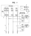
- FIGS. 1 to 5 are respectively a block diagram of a pixel array with M rows and N columns configuring a first embodiment, an equivalent circuit diagram of one pixel, a detailed diagram of a common output unit, a detailed diagram of an output buffer stage of a driving unit and a drive timing chart.
- FIG. 1 a pixel 1, a pixel array 2 in which pixels are arranged in a matrix with M rows and N columns, a constant current source 3 provided at each pixel column, and a common output line 4 for each pixel column are illustrated. It can be said that the constant current source 3 is provided at each of the common output lines 4.
- a signal holding unit 5 holds a signal which transmits through the common output line.
- the signal from an output node of a pixel is supplied to an input node of the signal holding unit.
- a selecting unit 6 selects and outputs the signal held in each of the signal holding units to a common output unit which will be described later.
- the selecting unit 6 is provided correspondingly to each of the signal holding units, and transfers a signal to an input node of the common output unit from an output node of the signal holding unit.
- a common output unit 7 is provided at signal holding units of a predetermined number.
- the common output unit 7 sequentially outputs signals of the signal holding units of a predetermined number to a post-stage.
- the common output unit performs impedance conversion between the signal holding unit and the post-stage circuit, or amplification of a signal when transmitting the signal to the post-stage circuit from the signal holding unit.
- An amplifying unit 8 includes the signal holding unit 5 to the common output unit 7.
- the solid-state imaging apparatus of the present embodiment has a configuration having a plurality of amplifying units 8.
- a driving unit 9 supplies a drive pulse for controlling drive of the selecting unit.
- An output stage 100 amplifies and outputs a control signal which is an origin of the drive pulse.
- a control signal line 200 is also provided.
- Each amplifying unit 8 is provided at pixel columns of a predetermined number (L columns in this case), and (N/L) amplifying units 8 are provided in total.
- Each of the amplifying units 8 includes L of signal holding units 5, L of selecting units 6 and one common output unit 7.
- FIG. 2 is an equivalent circuit diagram of the pixel 1.
- a photodiode 10 functions as a photoelectric conversion element.
- a transferring unit 11 transfers a signal charge which is generated by the photoelectric conversion element 10.
- an MOS transistor can be used.
- a signal charge of the photoelectric conversion element is transferred to a floating diffusion (hereinafter, FD) region 15 via the transferring unit 11.
- the FD region is electrically connected to an input node of a pixel amplifying part which will be described later.
- a reset unit 12 supplies a reference voltage to the FD region to reset the potential of the FD region.
- an MOS transistor can be used.
- An amplifying transistor 13 configures the pixel amplifying part.
- the amplifying transistor 13 configures a source follower circuit with the constant current source 3 of FIG. 1 .
- the input node of the pixel amplifying part is a gate of the amplifying transistor, and the gate and the FD region are electrically connected.
- a pixel selecting unit 14 selects a signal of a predetermined pixel column and outputs the signal to the common output line 4.
- a pixel selecting unit 14 selects a signal of a predetermined pixel column and outputs the signal to the common output line 4.
- an MOS transistor can be used.
- An output node 16 of the pixel is also illustrated.
- signals which control the transferring unit 11, the reset unit 12 and the pixel selecting unit 14 are set as PTX, PRES and PSEL, respectively.
- FIG. 3 illustrates the amplifying unit 8 of FIG. 1 in detail.
- An MOS transistor is used as the selecting unit 6.
- the common output unit 7 includes a differential amplifier 71, and a feedback capacitor 72 arranged in an electric path between one input node (inversion input terminal) and an output node of the differential amplifier.
- the common output unit 7 includes a feedback switch 73 arranged parallel with the feedback capacitor. The feedback switch 73 is arranged in a feedback path which connects an input and output nodes of the differential amplifying unit.
- An input node 74 and an output node 75 of the differential amplifier are illustrated. The input and output nodes of the differential amplifier function as the input and output nodes of the common output unit.
- the input node and the output node of the differential amplifying unit function as the input and output nodes of the common output unit.
- an MOS transistor can be used as a feedback switch.
- a reference level (VREF) is supplied to the other input node (non-inversion input terminal) of the differential amplifier.
- the common output unit configures a switched capacitor amplifier by these components.
- For selecting unit 6 a section of an MOS transistor is illustrated for describing a charge injection phenomenon.
- Drive pulses which control L of the selecting units 6 are set as PSW_1, PSW_2 ... and PSW_L. These drive pulses are supplied from the driving unit 9 through the control signal line 200.
- a signal which controls the feedback switch 73 is set as PCOR.
- the switched capacitor amplifier of the common output unit 7 is in a one-time amplification factor mode when the PCOR is in an ON state, and outputs VREF input in a normal rotation input terminal.
- the switched capacitor amplifier is in an amplification mode of which amplification factor is defined by a capacitance ratio of the signal holding unit 5 and the feedback capacitor 72.
- the signal holding unit functions as an input capacitor, and the amplification factor in the amplifying mode becomes CC/CF when the capacitance value of the signal holding unit 5 is set as CC, and the capacitance value of the feedback capacitor 72 is set as CF.
- the amplifying unit including the switch and the capacitor amplifier is configured to be operable by switching these operation modes.
- an input node 51 of the signal holding unit, and an output node 52 of the signal holding unit are included.
- a gate 61 and a source and drain regions 62 and 63 are also included.
- a channel region 64 is formed under the gate 61 via a gate insulating film when the selecting unit 6 is ON.
- an N type MOS transistor will be described as an example.
- a gate capacitor 65 is formed between the gate 61 and the channel 64. Overlap capacitors 66 and 67 which are formed between the gate 61, and the source 62 and the drain 63 are schematically illustrated.
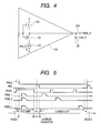
- FIG. 4 illustrates an output buffer stage 100 of the driving unit 9 of FIG. 1 in detail.
- the output buffer stage 100 has a P type MOS transistor 102 and an N type MOS transistor 103 having gates to which a control signal is supplied. Drains of the P type MOS transistor 102 and the N type MOS transistor 103 are connected to each other. A power source voltage is supplied to the source of the P type MOS transistor, and the source of the N type MOS transistor is grounded via the constant current source 101.
- a capacitor 201 which is added to the control signal line 200 is schematically illustrated.
- a capacitor added to the X-th control signal line 200 is set as Csw_X, and a current passing in the constant current source 101 of the output buffer stage of the X-th driving unit is set as Isw_X.
- a time Tfsw_X in which the PSW_X shifts from an ON state to an OFF state is inversely proportional to Isw_X, and proportional to the Csw_X. Accordingly, by changing them, the shifting time can be controlled.
- VDD maximum value of the pulse waveform
- the circuit is configured to supply a power source voltage directly to the source of the P type MOS transistor as shown in FIG. 4 .
- a constant current source with a larger drive force than the constant current source 101 is provided between the power source and the source of the P type MOS transistor.
- the drive timing chart of FIG. 5 will be described.
- the pixel array with M columns and N rows is configured.
- the MOS transistor 14 which is the pixel selecting unit is assumed to be in an ON state.
- Each of the switches is High active (ON state in an ON state).
- a reset signal PRES shifts to an OFF state to an ON state.
- the potential of the FD region is reset at a reference potential, and thereafter, as floating, a signal based on the reference potential is outputted to the common output line 4 via the source follower circuit.
- the drive pulse of an ON state is supplied to the feedback switch 73 of the switched capacitor amplifier, and the normal rotation input level VREF is outputted to the output node of the differential amplifier 71 in one time amplification factor mode.
- the charge amount which causes offset written to the signal holding capacitor 5 is determined by the size of the selecting unit 6. For example, when a maximum charge amount of the clock field through and charge injection which generate in the selecting unit 6 is set as Qsw_max, a maximum offset voltage Voff_max which is written into the signal holding capacitor 5 is what is obtained by dividing Qsw_max by a capacitance value CC of the signal holding capacitor 5. The offset amount written into the signal holding capacitor is further multiplied by CC/CF by the switched capacitor amplifier.
- the period in which the selecting unit 6 shifts to an OFF state from the ON state is ensured by properly designing the constant current source 101 of the output stage of the driving unit, and the capacitor added to the control signal line 200. Thereby, sufficient charges are supplied from the output node of the differential amplifier 71. As a result, the offset voltage which is written into the signal holding capacitor 5 can be reduced.
- a length Toff of the period in which the selecting unit 6 shifts to the OFF state from the ON state is properly 30 ns ⁇ Toff ⁇ 1 ⁇ s. This is because, with a length Toff of less than 30 ns, sufficient charges are not supplied from the output node of the differential amplifier 71, and the influence of the offset voltage becomes relatively large. Further, with a length Toff of more than 1 ⁇ s, the influence on the readout speed becomes large.
- the time in which the selecting unit 6 shifts to the ON state from the OFF state is irrelevant to the offset voltage.
- the circuit operation becomes slow. Therefore, pulse shift to the ON state from the OFF state is preferably performed in as short a time as possible.
- the time in which the selecting unit 6 shifts to the ON state from the OFF state needs to be made as short as possible, and the time in which it shifts to the OFF state from the ON state needs to be set to be long so that the offset voltage becomes sufficiently small.
- the time changing rate of the amplitude of the drive pulse when the selecting unit 6 shifts to the ON state from the OFF state is made small.
- FIG. 5 illustrates the pulse waveform. In t1 to t2, as compared with the rise of the pulse at the ON time, the drop of the pulse at the OFF time becomes a gradual change.
- the circuit configuration for achieving the time changing rate as described above can be configured with a circuit which extracts the charges of the wiring capacitor with a constant current, and the circuit using a switched capacitor, in addition to the method of using the circuit of FIG. 4 .
- PCOR is shifted to an OFF state from the ON state, and the switched capacitor amplifier of the common output unit 7 is brought into an amplification mode.
- a signal PTX which controls the transferring unit 11 is brought into an ON state, and brought into an OFF state at a time t4, and the charges accumulated in the photoelectric conversion element 10 are transferred to the FD region 15.
- the optical signal level corresponding to the signal charge is outputted to the common output line 4 via the source follower.
- PSW_1 to PSW_L and PCOR are alternately brought into an ON state and OFF state repeatedly, and thereby, the pixel outputs of one column of the pixel array 2 with pixels arranged in M rows and N columns are sequentially read out to the post-stage of the common output unit 7.
- each amplifying unit 8 at every L column, (N/L) amplifying units 8 in total, for the pixels arranged in M rows and N columns is described above, but the present embodiment is not limited to this.
- the number of columns may be only one. Further, a larger number of amplifying units may be provided.
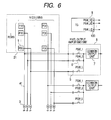
- FIG. 6 is a first modified example of FIG. 1 .
- a pixel array 21 with pixels 1 being arranged in L columns and N rows, and a pixel output line 41 are illustrated. Unlike the pixel array 2 of FIG. 1 , each pixel output line 41 is provided for each pixel, and the constant current source 3 is connected to each of the pixel output lines 41.
- the amplifying unit 8 is shared by a plurality of pixel columns. The present embodiment also can be applied to such a case.
- FIG. 10 is a second modified example.
- the present modified example is an example applied to a one-dimensional pixel array with pixels arranged in one row and N columns.
- the amplifying unit 8 is shared by a plurality of pixel columns. By sharing the amplifying unit by a plurality of pixels, the chip area of the linear sensor can be made small.
- the drive pulse waveform of FIG. 5 can be directly applied. In such a configuration, the present embodiment also can be applied.
- the solid-state imaging apparatus by reducing the offset due to electric charges by clock field through and charge injection, the solid-state imaging apparatus can be realized, which causes less fixed pattern noise even when the capacitance value of the signal holding unit 5 is made small.
- FIGS. 7 and 8 A second embodiment will be described by using FIGS. 7 and 8 .
- FIG. 7 is a circuit diagram in the case of using a digital analog converter with a drive circuit functioning as a ramp shaped wave generator circuit.
- FIG. 8 illustrates an input waveform and an output waveform of the circuit of FIG. 7 .
- DAC 300 a Digital Analog Converter (hereinafter, DAC) 300 is illustrated, and control signals DA_IO, DA_I1, DA_I2 and DA_I3 control the DAC 300.
- the DAC 300 with resolution of 4 bit is illustrated as an example.
- a PSW_X signal is generated by the control signals DA_I0 to DA_I3 from the four input nodes.
- Drive pulses differing in frequency and pulse width are supplied to DA_I0 to DA_I3.
- the waveform which ramps down by 16 steps from an ON state to an OFF state can be outputted.
- the aforementioned relation of the time changing rate can be realized by outputting the signals through an ordinary inverter instead of the DAC.
- the waveform of the drive pulse can be made an optional waveform.
- the DAC 300 can be given sufficient driving ability to the load of the control signal wiring, and therefore, the ramp waveform can be outputted without being influenced by the capacitor added to the output.
- an optional control waveform can be easily created, and the time changing rate of shift from the ON state to the OFF state can be easily set.
- a third embodiment will be described by using FIG. 9 .
- the present embodiment is an example of making the operation current of a constant current source changeable by monitoring the output from the drive circuit of a selecting unit, and feeding back the monitored result to the constant current source.
- FIG. 9 illustrates a variable constant current source 401, and a monitor circuit 400 which monitors the potential of the control signal line 200, and regulates a current value Iswv_X of the variable constant current source 401 from the monitored result.
- a feedback path (not illustrated) from the monitor circuit to the variable constant current source 401 is provided.
- the capacitance value added to the X-th control signal line 200 is set as Csw_X
- a current defined by the output stage constant current source 101 of the X-th control signal supply unit is set as Iswv_X
- the monitor circuit 400 the potential of the control signal line 200 is monitored, and the variation amount is fed back to the variable constant current source.
- Iswv_X is regulated so that Tfsw_X becomes constant, the output buffer stage 100 with influence of the variation of Csw_X being suppressed can be configured.
- influence of variation of Csw_X can be further suppressed, and influence on the signal can be suppressed.
- the present invention is described above by citing the embodiments. However, the present invention is not limited to these embodiments.
- all the waveforms of the pulses PSW_1 to PSW_L have small changing rates from the ON state to the OFF state, but such waveforms need to be obtained at least in the pulses supplied in the period of t1 to t2.
- the pulses which are supplied in the period t1 to t2 are, in other words, the pulses which are supplied in the period in which the reference signals for clamp operation are supplied to the signal holding unit 5.
- the signal charge is an electron is described, but the signal charge may be a hole.
- the pixel configuration may be such that the amplifying unit and the like are shared by a plurality of photoelectric conversion elements.
- the time changing rate at the time of shifting to the ON state from the OFF state may be made smaller than at the time of shifting from the ON state to the OFF state by generating the pulse at an intermediate potential, for example, and holding the pulse at the intermediate potential for a constant period.
- a solid-state imaging apparatus of the present invention is characterized in that, when a clamp operation of a pixel output signal is performed in the signal holding unit, a time changing rate of an amplitude of a drive pulse supplied to the selecting unit for turning from a non-conducting state to a conducting state is not larger than a time changing rate of the amplitude of the drive pulse supplied to the selecting unit for turning from the conducting state to the non-conducting state.
Landscapes
- Engineering & Computer Science (AREA)
- Multimedia (AREA)
- Signal Processing (AREA)
- Transforming Light Signals Into Electric Signals (AREA)
- Solid State Image Pick-Up Elements (AREA)
- Picture Signal Circuits (AREA)
- Computer Vision & Pattern Recognition (AREA)
Applications Claiming Priority (1)
| Application Number | Priority Date | Filing Date | Title |
|---|---|---|---|
| JP2008171731A JP5224942B2 (ja) | 2008-06-30 | 2008-06-30 | 固体撮像装置 |
Publications (3)
| Publication Number | Publication Date |
|---|---|
| EP2141908A2 true EP2141908A2 (fr) | 2010-01-06 |
| EP2141908A3 EP2141908A3 (fr) | 2013-02-20 |
| EP2141908B1 EP2141908B1 (fr) | 2014-12-31 |
Family
ID=41339028
Family Applications (1)
| Application Number | Title | Priority Date | Filing Date |
|---|---|---|---|
| EP09162809.9A Not-in-force EP2141908B1 (fr) | 2008-06-30 | 2009-06-16 | Appareil d'imagerie à semi-conducteur |
Country Status (4)
| Country | Link |
|---|---|
| US (2) | US8553118B2 (fr) |
| EP (1) | EP2141908B1 (fr) |
| JP (1) | JP5224942B2 (fr) |
| CN (1) | CN101621637B (fr) |
Cited By (1)
| Publication number | Priority date | Publication date | Assignee | Title |
|---|---|---|---|---|
| US9848149B2 (en) | 2010-11-30 | 2017-12-19 | Semiconductor Energy Laboratory Co., Ltd. | Method for driving photosensor, method for driving semiconductor device, semiconductor device, and electronic device |
Families Citing this family (47)
| Publication number | Priority date | Publication date | Assignee | Title |
|---|---|---|---|---|
| JP5224942B2 (ja) * | 2008-06-30 | 2013-07-03 | キヤノン株式会社 | 固体撮像装置 |
| JP5225145B2 (ja) * | 2009-02-23 | 2013-07-03 | キヤノン株式会社 | 固体撮像装置 |
| JP5322696B2 (ja) * | 2009-02-25 | 2013-10-23 | キヤノン株式会社 | 固体撮像装置及びその駆動方法 |
| JP5495701B2 (ja) * | 2009-10-07 | 2014-05-21 | キヤノン株式会社 | 固体撮像装置 |
| JP5808162B2 (ja) * | 2011-06-23 | 2015-11-10 | キヤノン株式会社 | 撮像素子、撮像装置及び撮像素子の駆動方法 |
| JP5762199B2 (ja) | 2011-07-28 | 2015-08-12 | キヤノン株式会社 | 固体撮像装置 |
| JP5901186B2 (ja) | 2011-09-05 | 2016-04-06 | キヤノン株式会社 | 固体撮像装置及びその駆動方法 |
| JP5858695B2 (ja) | 2011-09-08 | 2016-02-10 | キヤノン株式会社 | 固体撮像装置及び固体撮像装置の駆動方法 |
| JP5806566B2 (ja) | 2011-09-15 | 2015-11-10 | キヤノン株式会社 | A/d変換器および固体撮像装置 |
| JP5801665B2 (ja) | 2011-09-15 | 2015-10-28 | キヤノン株式会社 | 固体撮像装置、a/d変換器およびその制御方法 |
| JP5930651B2 (ja) | 2011-10-07 | 2016-06-08 | キヤノン株式会社 | 固体撮像装置 |
| JP5901212B2 (ja) | 2011-10-07 | 2016-04-06 | キヤノン株式会社 | 光電変換システム |
| JP5484422B2 (ja) | 2011-10-07 | 2014-05-07 | キヤノン株式会社 | 固体撮像装置 |
| JP6060500B2 (ja) * | 2012-03-01 | 2017-01-18 | 株式会社ニコン | 撮像素子 |
| JP2013200187A (ja) * | 2012-03-23 | 2013-10-03 | Toshiba Corp | 非冷却型赤外線撮像装置 |
| JP6057602B2 (ja) | 2012-08-10 | 2017-01-11 | キヤノン株式会社 | 固体撮像装置 |
| JP2014120858A (ja) | 2012-12-14 | 2014-06-30 | Canon Inc | 固体撮像装置 |
| JP6075393B2 (ja) * | 2013-05-31 | 2017-02-08 | 株式会社ニコン | 電子機器及び制御プログラム |
| KR20150018723A (ko) * | 2013-08-09 | 2015-02-24 | 에스케이하이닉스 주식회사 | 버퍼 회로 |
| JP6274898B2 (ja) * | 2014-02-17 | 2018-02-07 | キヤノン株式会社 | 固体撮像装置及びカメラ |
| JP6351288B2 (ja) | 2014-02-17 | 2018-07-04 | キヤノン株式会社 | 固体撮像装置及び撮像システム |
| JP6341688B2 (ja) | 2014-02-25 | 2018-06-13 | キヤノン株式会社 | 固体撮像装置及び撮像システム |
| JP6595750B2 (ja) | 2014-03-14 | 2019-10-23 | キヤノン株式会社 | 固体撮像装置及び撮像システム |
| US9484134B2 (en) * | 2014-03-26 | 2016-11-01 | Mediatek Inc. | Feedthrough signal transmission circuit and method utilizing permanently on buffer and switchable normal buffer |
| JP6541347B2 (ja) | 2014-03-27 | 2019-07-10 | キヤノン株式会社 | 固体撮像装置および撮像システム |
| JP6548391B2 (ja) | 2014-03-31 | 2019-07-24 | キヤノン株式会社 | 光電変換装置および撮像システム |
| JP6218799B2 (ja) * | 2015-01-05 | 2017-10-25 | キヤノン株式会社 | 撮像素子及び撮像装置 |
| US10003761B2 (en) | 2015-09-10 | 2018-06-19 | Canon Kabushiki Kaisha | Imaging device having multiple analog-digital conversion circuits that perform multiple ad conversions for a singular one of a pixel signal |
| US9900539B2 (en) | 2015-09-10 | 2018-02-20 | Canon Kabushiki Kaisha | Solid-state image pickup element, and image pickup system |
| JP6674224B2 (ja) | 2015-10-22 | 2020-04-01 | キヤノン株式会社 | 固体撮像装置 |
| JP6677594B2 (ja) | 2016-06-30 | 2020-04-08 | キヤノン株式会社 | 光電変換装置 |
| JP6856983B2 (ja) | 2016-06-30 | 2021-04-14 | キヤノン株式会社 | 光電変換装置及びカメラ |
| JP6740067B2 (ja) * | 2016-09-16 | 2020-08-12 | キヤノン株式会社 | 固体撮像装置及びその駆動方法 |
| JP6750876B2 (ja) | 2016-10-07 | 2020-09-02 | キヤノン株式会社 | 固体撮像装置及びその駆動方法 |
| JP2018082261A (ja) | 2016-11-15 | 2018-05-24 | キヤノン株式会社 | 撮像素子 |
| JP6946046B2 (ja) | 2017-04-28 | 2021-10-06 | キヤノン株式会社 | 光電変換装置及びその駆動方法 |
| JP7057635B2 (ja) | 2017-08-15 | 2022-04-20 | キヤノン株式会社 | 撮像装置、カメラおよび輸送機器 |
| JP7046551B2 (ja) | 2017-10-03 | 2022-04-04 | キヤノン株式会社 | 固体撮像装置及び撮像システム |
| JP6704893B2 (ja) | 2017-11-30 | 2020-06-03 | キヤノン株式会社 | 固体撮像装置、撮像システム、および固体撮像装置の駆動方法 |
| US10462397B1 (en) * | 2018-05-17 | 2019-10-29 | Sony Semiconductor Solutions Corporation | Sample-and-hold circuit with feedback and noise integration |
| JP7286309B2 (ja) | 2018-12-18 | 2023-06-05 | キヤノン株式会社 | 光電変換装置、光電変換システムおよび信号処理装置 |
| JP6694090B1 (ja) * | 2019-03-01 | 2020-05-13 | 力晶積成電子製造股▲ふん▼有限公司Powerchip Semiconductor Manufacturing Corporation | Da変換回路、不良ビット数検出回路及び不揮発性半導体記憶装置 |
| JP7358079B2 (ja) | 2019-06-10 | 2023-10-10 | キヤノン株式会社 | 撮像装置、撮像システムおよび半導体チップ |
| JP7303682B2 (ja) | 2019-07-19 | 2023-07-05 | キヤノン株式会社 | 光電変換装置及び撮像システム |
| JP7374639B2 (ja) | 2019-07-19 | 2023-11-07 | キヤノン株式会社 | 光電変換装置及び撮像システム |
| JP7451139B2 (ja) * | 2019-10-30 | 2024-03-18 | キヤノン株式会社 | 光電変換装置及び撮像システム |
| JP7171649B2 (ja) | 2020-05-15 | 2022-11-15 | キヤノン株式会社 | 撮像装置および撮像システム |
Citations (1)
| Publication number | Priority date | Publication date | Assignee | Title |
|---|---|---|---|---|
| JP2003228457A (ja) | 2001-10-16 | 2003-08-15 | Agilent Technol Inc | 複数列に単一の増幅器を用いる順次読み出しシステム |
Family Cites Families (17)
| Publication number | Priority date | Publication date | Assignee | Title |
|---|---|---|---|---|
| FR2699023B1 (fr) * | 1992-12-09 | 1995-02-24 | Texas Instruments France | Circuit à retard commandé. |
| US6885396B1 (en) * | 1998-03-09 | 2005-04-26 | Micron Technology, Inc. | Readout circuit with gain and analog-to-digital a conversion for image sensor |
| US6222175B1 (en) * | 1998-03-10 | 2001-04-24 | Photobit Corporation | Charge-domain analog readout for an image sensor |
| JP2000346950A (ja) * | 1999-06-07 | 2000-12-15 | Toshiba Corp | 放射線検出器 |
| US6873364B1 (en) * | 2000-06-08 | 2005-03-29 | Micron Technology, Inc. | Low-power signal chain for image sensors |
| JP3667214B2 (ja) * | 2000-08-25 | 2005-07-06 | キヤノン株式会社 | 固体撮像装置およびその駆動方法 |
| WO2004102805A1 (fr) * | 2003-05-13 | 2004-11-25 | Fujitsu Limited | Circuit a retard |
| US7388608B2 (en) * | 2004-03-11 | 2008-06-17 | Micron Technology, Inc. | Sample and hold circuit and active pixel sensor array sampling system utilizing same |
| JP2005303746A (ja) * | 2004-04-13 | 2005-10-27 | Matsushita Electric Ind Co Ltd | 撮像装置 |
| JP2006101479A (ja) * | 2004-09-02 | 2006-04-13 | Canon Inc | 固体撮像装置及びそれを用いたカメラ |
| JP4208892B2 (ja) * | 2006-05-01 | 2009-01-14 | キヤノン株式会社 | 固体撮像装置 |
| US7746400B2 (en) | 2007-07-31 | 2010-06-29 | Aptina Imaging Corporation | Method, apparatus, and system providing multi-column shared readout for imagers |
| JP5004775B2 (ja) * | 2007-12-04 | 2012-08-22 | キヤノン株式会社 | 撮像装置及び撮像システム |
| JP5224942B2 (ja) * | 2008-06-30 | 2013-07-03 | キヤノン株式会社 | 固体撮像装置 |
| JP5311954B2 (ja) * | 2008-09-30 | 2013-10-09 | キヤノン株式会社 | 固体撮像装置の駆動方法 |
| KR101688600B1 (ko) * | 2010-04-14 | 2016-12-23 | 삼성전자 주식회사 | 피드백 클램프블록을 구비하는 샘플링회로, 영상신호증폭회로 및 상기 영상신호증폭회로를 구비하는 이미지센서 |
| JP6057602B2 (ja) * | 2012-08-10 | 2017-01-11 | キヤノン株式会社 | 固体撮像装置 |
-
2008
- 2008-06-30 JP JP2008171731A patent/JP5224942B2/ja not_active Expired - Fee Related
-
2009
- 2009-05-29 US US12/474,805 patent/US8553118B2/en not_active Expired - Fee Related
- 2009-06-16 EP EP09162809.9A patent/EP2141908B1/fr not_active Not-in-force
- 2009-06-30 CN CN200910151316XA patent/CN101621637B/zh not_active Expired - Fee Related
-
2013
- 2013-09-06 US US14/020,409 patent/US9337222B2/en not_active Expired - Fee Related
Patent Citations (1)
| Publication number | Priority date | Publication date | Assignee | Title |
|---|---|---|---|---|
| JP2003228457A (ja) | 2001-10-16 | 2003-08-15 | Agilent Technol Inc | 複数列に単一の増幅器を用いる順次読み出しシステム |
Cited By (1)
| Publication number | Priority date | Publication date | Assignee | Title |
|---|---|---|---|---|
| US9848149B2 (en) | 2010-11-30 | 2017-12-19 | Semiconductor Energy Laboratory Co., Ltd. | Method for driving photosensor, method for driving semiconductor device, semiconductor device, and electronic device |
Also Published As
| Publication number | Publication date |
|---|---|
| EP2141908B1 (fr) | 2014-12-31 |
| JP5224942B2 (ja) | 2013-07-03 |
| JP2010011426A (ja) | 2010-01-14 |
| EP2141908A3 (fr) | 2013-02-20 |
| CN101621637A (zh) | 2010-01-06 |
| CN101621637B (zh) | 2011-07-20 |
| US20090322922A1 (en) | 2009-12-31 |
| US20140008522A1 (en) | 2014-01-09 |
| US9337222B2 (en) | 2016-05-10 |
| US8553118B2 (en) | 2013-10-08 |
Similar Documents
| Publication | Publication Date | Title |
|---|---|---|
| EP2141908B1 (fr) | Appareil d'imagerie à semi-conducteur | |
| CN101534397B (zh) | 固态图像拾取装置 | |
| US8605182B2 (en) | Driving method of solid-state imaging apparatus with successive clamping | |
| KR100463859B1 (ko) | 물리량 분포 검지 반도체 장치 및 그 구동방법 | |
| JP5250474B2 (ja) | 固体撮像装置 | |
| US8115847B2 (en) | Solid-state imaging apparatus and driving method suppressing a pseudo signal originated from an amplifying transistor and having less fixed pattern noises and shading | |
| US8605178B2 (en) | Solid-state imaging apparatus and method for driving the same | |
| WO2014132822A1 (fr) | Dispositif d'imagerie à semi-conducteurs, procédé de commande et dispositif électronique | |
| EP2433421A1 (fr) | Dispositif de capture d'image, système de capture d'image, et procédé de commande de dispositif de capture d'image | |
| US9549138B2 (en) | Imaging device, imaging system, and driving method of imaging device using comparator in analog-to-digital converter | |
| KR20060044736A (ko) | 증폭형 고체 촬상 장치 | |
| KR100619126B1 (ko) | kTC 잡음을 저감한 CMOS 이미지 센서, 그 이미지센서에 사용하는 리셋 트랜지스터 제어 회로, 및 그 제어회로에 사용하는 전압 전환 회로 | |
| US20150319388A1 (en) | Driving method for an image pickup apparatus, image pickup apparatus, and image pickup system | |
| WO2011027508A1 (fr) | Dispositif de prise d'image à semi-conducteurs | |
| JP2009290703A (ja) | 固体撮像装置およびカメラ | |
| CN102256069A (zh) | 固态成像设备 | |
| US20130119235A1 (en) | Solid-state imaging apparatus and method for driving solid-state imaging apparatus | |
| US20140085521A1 (en) | Image pickup apparatus, method of driving image pickup apparatus, and image pickup system | |
| US8723099B2 (en) | Solid-state imaging apparatus | |
| JP4336544B2 (ja) | 固体撮像装置 | |
| JP2001197378A (ja) | 固体撮像素子 | |
| JP2007166449A (ja) | 固体撮像素子のcds回路 | |
| US12120440B2 (en) | Image sensor | |
| US9197831B2 (en) | Photoelectric conversion system | |
| JP4655785B2 (ja) | 固体撮像素子の駆動方法 |
Legal Events
| Date | Code | Title | Description |
|---|---|---|---|
| PUAI | Public reference made under article 153(3) epc to a published international application that has entered the european phase |
Free format text: ORIGINAL CODE: 0009012 |
|
| AK | Designated contracting states |
Kind code of ref document: A2 Designated state(s): AT BE BG CH CY CZ DE DK EE ES FI FR GB GR HR HU IE IS IT LI LT LU LV MC MK MT NL NO PL PT RO SE SI SK TR |
|
| PUAL | Search report despatched |
Free format text: ORIGINAL CODE: 0009013 |
|
| AK | Designated contracting states |
Kind code of ref document: A3 Designated state(s): AT BE BG CH CY CZ DE DK EE ES FI FR GB GR HR HU IE IS IT LI LT LU LV MC MK MT NL NO PL PT RO SE SI SK TR |
|
| AX | Request for extension of the european patent |
Extension state: AL BA RS |
|
| 17P | Request for examination filed |
Effective date: 20130820 |
|
| RBV | Designated contracting states (corrected) |
Designated state(s): AT BE BG CH CY CZ DE DK EE ES FI FR GB GR HR HU IE IS IT LI LT LU LV MC MK MT NL NO PL PT RO SE SI SK TR |
|
| REG | Reference to a national code |
Ref country code: DE Ref legal event code: R079 Ref document number: 602009028643 Country of ref document: DE Free format text: PREVIOUS MAIN CLASS: H04N0003150000 Ipc: H04N0005378000 |
|
| GRAP | Despatch of communication of intention to grant a patent |
Free format text: ORIGINAL CODE: EPIDOSNIGR1 |
|
| RIC1 | Information provided on ipc code assigned before grant |
Ipc: H01L 27/146 20060101ALI20140709BHEP Ipc: H04N 5/365 20110101ALI20140709BHEP Ipc: H04N 3/14 20060101ALI20140709BHEP Ipc: H04N 5/378 20110101AFI20140709BHEP |
|
| INTG | Intention to grant announced |
Effective date: 20140724 |
|
| GRAS | Grant fee paid |
Free format text: ORIGINAL CODE: EPIDOSNIGR3 |
|
| GRAA | (expected) grant |
Free format text: ORIGINAL CODE: 0009210 |
|
| AK | Designated contracting states |
Kind code of ref document: B1 Designated state(s): AT BE BG CH CY CZ DE DK EE ES FI FR GB GR HR HU IE IS IT LI LT LU LV MC MK MT NL NO PL PT RO SE SI SK TR |
|
| REG | Reference to a national code |
Ref country code: CH Ref legal event code: EP Ref country code: GB Ref legal event code: FG4D |
|
| REG | Reference to a national code |
Ref country code: IE Ref legal event code: FG4D |
|
| REG | Reference to a national code |
Ref country code: AT Ref legal event code: REF Ref document number: 704966 Country of ref document: AT Kind code of ref document: T Effective date: 20150215 |
|
| REG | Reference to a national code |
Ref country code: DE Ref legal event code: R096 Ref document number: 602009028643 Country of ref document: DE Effective date: 20150219 |
|
| PG25 | Lapsed in a contracting state [announced via postgrant information from national office to epo] |
Ref country code: LT Free format text: LAPSE BECAUSE OF FAILURE TO SUBMIT A TRANSLATION OF THE DESCRIPTION OR TO PAY THE FEE WITHIN THE PRESCRIBED TIME-LIMIT Effective date: 20141231 Ref country code: FI Free format text: LAPSE BECAUSE OF FAILURE TO SUBMIT A TRANSLATION OF THE DESCRIPTION OR TO PAY THE FEE WITHIN THE PRESCRIBED TIME-LIMIT Effective date: 20141231 Ref country code: NO Free format text: LAPSE BECAUSE OF FAILURE TO SUBMIT A TRANSLATION OF THE DESCRIPTION OR TO PAY THE FEE WITHIN THE PRESCRIBED TIME-LIMIT Effective date: 20150331 |
|
| REG | Reference to a national code |
Ref country code: NL Ref legal event code: VDEP Effective date: 20141231 |
|
| REG | Reference to a national code |
Ref country code: LT Ref legal event code: MG4D |
|
| PG25 | Lapsed in a contracting state [announced via postgrant information from national office to epo] |
Ref country code: SE Free format text: LAPSE BECAUSE OF FAILURE TO SUBMIT A TRANSLATION OF THE DESCRIPTION OR TO PAY THE FEE WITHIN THE PRESCRIBED TIME-LIMIT Effective date: 20141231 Ref country code: LV Free format text: LAPSE BECAUSE OF FAILURE TO SUBMIT A TRANSLATION OF THE DESCRIPTION OR TO PAY THE FEE WITHIN THE PRESCRIBED TIME-LIMIT Effective date: 20141231 Ref country code: HR Free format text: LAPSE BECAUSE OF FAILURE TO SUBMIT A TRANSLATION OF THE DESCRIPTION OR TO PAY THE FEE WITHIN THE PRESCRIBED TIME-LIMIT Effective date: 20141231 Ref country code: GR Free format text: LAPSE BECAUSE OF FAILURE TO SUBMIT A TRANSLATION OF THE DESCRIPTION OR TO PAY THE FEE WITHIN THE PRESCRIBED TIME-LIMIT Effective date: 20150401 |
|
| REG | Reference to a national code |
Ref country code: AT Ref legal event code: MK05 Ref document number: 704966 Country of ref document: AT Kind code of ref document: T Effective date: 20141231 |
|
| PG25 | Lapsed in a contracting state [announced via postgrant information from national office to epo] |
Ref country code: NL Free format text: LAPSE BECAUSE OF FAILURE TO SUBMIT A TRANSLATION OF THE DESCRIPTION OR TO PAY THE FEE WITHIN THE PRESCRIBED TIME-LIMIT Effective date: 20141231 |
|
| PG25 | Lapsed in a contracting state [announced via postgrant information from national office to epo] |
Ref country code: ES Free format text: LAPSE BECAUSE OF FAILURE TO SUBMIT A TRANSLATION OF THE DESCRIPTION OR TO PAY THE FEE WITHIN THE PRESCRIBED TIME-LIMIT Effective date: 20141231 Ref country code: RO Free format text: LAPSE BECAUSE OF FAILURE TO SUBMIT A TRANSLATION OF THE DESCRIPTION OR TO PAY THE FEE WITHIN THE PRESCRIBED TIME-LIMIT Effective date: 20141231 Ref country code: SK Free format text: LAPSE BECAUSE OF FAILURE TO SUBMIT A TRANSLATION OF THE DESCRIPTION OR TO PAY THE FEE WITHIN THE PRESCRIBED TIME-LIMIT Effective date: 20141231 Ref country code: CZ Free format text: LAPSE BECAUSE OF FAILURE TO SUBMIT A TRANSLATION OF THE DESCRIPTION OR TO PAY THE FEE WITHIN THE PRESCRIBED TIME-LIMIT Effective date: 20141231 |
|
| PG25 | Lapsed in a contracting state [announced via postgrant information from national office to epo] |
Ref country code: AT Free format text: LAPSE BECAUSE OF FAILURE TO SUBMIT A TRANSLATION OF THE DESCRIPTION OR TO PAY THE FEE WITHIN THE PRESCRIBED TIME-LIMIT Effective date: 20141231 Ref country code: IS Free format text: LAPSE BECAUSE OF FAILURE TO SUBMIT A TRANSLATION OF THE DESCRIPTION OR TO PAY THE FEE WITHIN THE PRESCRIBED TIME-LIMIT Effective date: 20150430 Ref country code: PL Free format text: LAPSE BECAUSE OF FAILURE TO SUBMIT A TRANSLATION OF THE DESCRIPTION OR TO PAY THE FEE WITHIN THE PRESCRIBED TIME-LIMIT Effective date: 20141231 |
|
| REG | Reference to a national code |
Ref country code: DE Ref legal event code: R097 Ref document number: 602009028643 Country of ref document: DE |
|
| PG25 | Lapsed in a contracting state [announced via postgrant information from national office to epo] |
Ref country code: DK Free format text: LAPSE BECAUSE OF FAILURE TO SUBMIT A TRANSLATION OF THE DESCRIPTION OR TO PAY THE FEE WITHIN THE PRESCRIBED TIME-LIMIT Effective date: 20141231 Ref country code: EE Free format text: LAPSE BECAUSE OF FAILURE TO SUBMIT A TRANSLATION OF THE DESCRIPTION OR TO PAY THE FEE WITHIN THE PRESCRIBED TIME-LIMIT Effective date: 20141231 |
|
| PLBE | No opposition filed within time limit |
Free format text: ORIGINAL CODE: 0009261 |
|
| STAA | Information on the status of an ep patent application or granted ep patent |
Free format text: STATUS: NO OPPOSITION FILED WITHIN TIME LIMIT |
|
| 26N | No opposition filed |
Effective date: 20151001 |
|
| PG25 | Lapsed in a contracting state [announced via postgrant information from national office to epo] |
Ref country code: IT Free format text: LAPSE BECAUSE OF FAILURE TO SUBMIT A TRANSLATION OF THE DESCRIPTION OR TO PAY THE FEE WITHIN THE PRESCRIBED TIME-LIMIT Effective date: 20141231 |
|
| PG25 | Lapsed in a contracting state [announced via postgrant information from national office to epo] |
Ref country code: MC Free format text: LAPSE BECAUSE OF FAILURE TO SUBMIT A TRANSLATION OF THE DESCRIPTION OR TO PAY THE FEE WITHIN THE PRESCRIBED TIME-LIMIT Effective date: 20141231 |
|
| REG | Reference to a national code |
Ref country code: CH Ref legal event code: PL |
|
| PG25 | Lapsed in a contracting state [announced via postgrant information from national office to epo] |
Ref country code: SI Free format text: LAPSE BECAUSE OF FAILURE TO SUBMIT A TRANSLATION OF THE DESCRIPTION OR TO PAY THE FEE WITHIN THE PRESCRIBED TIME-LIMIT Effective date: 20141231 Ref country code: LU Free format text: LAPSE BECAUSE OF FAILURE TO SUBMIT A TRANSLATION OF THE DESCRIPTION OR TO PAY THE FEE WITHIN THE PRESCRIBED TIME-LIMIT Effective date: 20150616 |
|
| REG | Reference to a national code |
Ref country code: IE Ref legal event code: MM4A |
|
| REG | Reference to a national code |
Ref country code: FR Ref legal event code: ST Effective date: 20160229 |
|
| PG25 | Lapsed in a contracting state [announced via postgrant information from national office to epo] |
Ref country code: LI Free format text: LAPSE BECAUSE OF NON-PAYMENT OF DUE FEES Effective date: 20150630 Ref country code: CH Free format text: LAPSE BECAUSE OF NON-PAYMENT OF DUE FEES Effective date: 20150630 Ref country code: IE Free format text: LAPSE BECAUSE OF NON-PAYMENT OF DUE FEES Effective date: 20150616 |
|
| PG25 | Lapsed in a contracting state [announced via postgrant information from national office to epo] |
Ref country code: BE Free format text: LAPSE BECAUSE OF FAILURE TO SUBMIT A TRANSLATION OF THE DESCRIPTION OR TO PAY THE FEE WITHIN THE PRESCRIBED TIME-LIMIT Effective date: 20141231 Ref country code: FR Free format text: LAPSE BECAUSE OF NON-PAYMENT OF DUE FEES Effective date: 20150630 |
|
| PG25 | Lapsed in a contracting state [announced via postgrant information from national office to epo] |
Ref country code: MT Free format text: LAPSE BECAUSE OF FAILURE TO SUBMIT A TRANSLATION OF THE DESCRIPTION OR TO PAY THE FEE WITHIN THE PRESCRIBED TIME-LIMIT Effective date: 20141231 |
|
| PG25 | Lapsed in a contracting state [announced via postgrant information from national office to epo] |
Ref country code: HU Free format text: LAPSE BECAUSE OF FAILURE TO SUBMIT A TRANSLATION OF THE DESCRIPTION OR TO PAY THE FEE WITHIN THE PRESCRIBED TIME-LIMIT; INVALID AB INITIO Effective date: 20090616 Ref country code: BG Free format text: LAPSE BECAUSE OF FAILURE TO SUBMIT A TRANSLATION OF THE DESCRIPTION OR TO PAY THE FEE WITHIN THE PRESCRIBED TIME-LIMIT Effective date: 20141231 |
|
| PG25 | Lapsed in a contracting state [announced via postgrant information from national office to epo] |
Ref country code: CY Free format text: LAPSE BECAUSE OF FAILURE TO SUBMIT A TRANSLATION OF THE DESCRIPTION OR TO PAY THE FEE WITHIN THE PRESCRIBED TIME-LIMIT Effective date: 20141231 |
|
| PG25 | Lapsed in a contracting state [announced via postgrant information from national office to epo] |
Ref country code: TR Free format text: LAPSE BECAUSE OF FAILURE TO SUBMIT A TRANSLATION OF THE DESCRIPTION OR TO PAY THE FEE WITHIN THE PRESCRIBED TIME-LIMIT Effective date: 20141231 |
|
| PG25 | Lapsed in a contracting state [announced via postgrant information from national office to epo] |
Ref country code: MK Free format text: LAPSE BECAUSE OF FAILURE TO SUBMIT A TRANSLATION OF THE DESCRIPTION OR TO PAY THE FEE WITHIN THE PRESCRIBED TIME-LIMIT Effective date: 20141231 |
|
| PG25 | Lapsed in a contracting state [announced via postgrant information from national office to epo] |
Ref country code: PT Free format text: LAPSE BECAUSE OF FAILURE TO SUBMIT A TRANSLATION OF THE DESCRIPTION OR TO PAY THE FEE WITHIN THE PRESCRIBED TIME-LIMIT Effective date: 20141231 |
|
| PGFP | Annual fee paid to national office [announced via postgrant information from national office to epo] |
Ref country code: DE Payment date: 20180831 Year of fee payment: 10 Ref country code: GB Payment date: 20180629 Year of fee payment: 10 |
|
| REG | Reference to a national code |
Ref country code: DE Ref legal event code: R119 Ref document number: 602009028643 Country of ref document: DE |
|
| GBPC | Gb: european patent ceased through non-payment of renewal fee |
Effective date: 20190616 |
|
| PG25 | Lapsed in a contracting state [announced via postgrant information from national office to epo] |
Ref country code: GB Free format text: LAPSE BECAUSE OF NON-PAYMENT OF DUE FEES Effective date: 20190616 Ref country code: DE Free format text: LAPSE BECAUSE OF NON-PAYMENT OF DUE FEES Effective date: 20200101 |