EP1864289B1 - Utilisation de verrous de donnees dans des operations de cache de memoire non volatile - Google Patents
Utilisation de verrous de donnees dans des operations de cache de memoire non volatile Download PDFInfo
- Publication number
- EP1864289B1 EP1864289B1 EP06739812A EP06739812A EP1864289B1 EP 1864289 B1 EP1864289 B1 EP 1864289B1 EP 06739812 A EP06739812 A EP 06739812A EP 06739812 A EP06739812 A EP 06739812A EP 1864289 B1 EP1864289 B1 EP 1864289B1
- Authority
- EP
- European Patent Office
- Prior art keywords
- data
- page
- read
- memory
- write
- Prior art date
- Legal status (The legal status is an assumption and is not a legal conclusion. Google has not performed a legal analysis and makes no representation as to the accuracy of the status listed.)
- Not-in-force
Links
- 230000015654 memory Effects 0.000 title claims abstract description 184
- 238000000034 method Methods 0.000 claims abstract description 50
- 238000012546 transfer Methods 0.000 abstract description 15
- 238000007667 floating Methods 0.000 description 31
- 230000008569 process Effects 0.000 description 31
- 238000006243 chemical reaction Methods 0.000 description 15
- 238000012795 verification Methods 0.000 description 8
- 230000006870 function Effects 0.000 description 7
- 230000008878 coupling Effects 0.000 description 6
- 238000010168 coupling process Methods 0.000 description 6
- 238000005859 coupling reaction Methods 0.000 description 6
- 239000000758 substrate Substances 0.000 description 6
- 238000004891 communication Methods 0.000 description 5
- 238000013461 design Methods 0.000 description 5
- 101001072191 Homo sapiens Protein disulfide-isomerase A2 Proteins 0.000 description 4
- 101001098828 Homo sapiens Protein disulfide-isomerase A5 Proteins 0.000 description 4
- 102100036351 Protein disulfide-isomerase A2 Human genes 0.000 description 4
- 238000010586 diagram Methods 0.000 description 4
- 230000007246 mechanism Effects 0.000 description 4
- 230000008901 benefit Effects 0.000 description 3
- 230000000295 complement effect Effects 0.000 description 3
- 238000009792 diffusion process Methods 0.000 description 3
- 238000002347 injection Methods 0.000 description 3
- 239000007924 injection Substances 0.000 description 3
- 230000004048 modification Effects 0.000 description 3
- 238000012986 modification Methods 0.000 description 3
- 238000001745 non-dispersive infrared spectroscopy Methods 0.000 description 3
- 239000004065 semiconductor Substances 0.000 description 3
- 230000007704 transition Effects 0.000 description 3
- VYPSYNLAJGMNEJ-UHFFFAOYSA-N Silicium dioxide Chemical compound O=[Si]=O VYPSYNLAJGMNEJ-UHFFFAOYSA-N 0.000 description 2
- 230000001419 dependent effect Effects 0.000 description 2
- 230000000694 effects Effects 0.000 description 2
- 230000005684 electric field Effects 0.000 description 2
- 239000002784 hot electron Substances 0.000 description 2
- 230000016507 interphase Effects 0.000 description 2
- 238000004519 manufacturing process Methods 0.000 description 2
- 238000005192 partition Methods 0.000 description 2
- 230000002093 peripheral effect Effects 0.000 description 2
- 229910021420 polycrystalline silicon Inorganic materials 0.000 description 2
- 229920005591 polysilicon Polymers 0.000 description 2
- 238000012545 processing Methods 0.000 description 2
- 230000005855 radiation Effects 0.000 description 2
- 238000000638 solvent extraction Methods 0.000 description 2
- 230000005689 Fowler Nordheim tunneling Effects 0.000 description 1
- 230000008859 change Effects 0.000 description 1
- 238000013500 data storage Methods 0.000 description 1
- 238000001514 detection method Methods 0.000 description 1
- 238000007599 discharging Methods 0.000 description 1
- 230000009977 dual effect Effects 0.000 description 1
- 238000005516 engineering process Methods 0.000 description 1
- 230000005669 field effect Effects 0.000 description 1
- 230000005283 ground state Effects 0.000 description 1
- 230000006872 improvement Effects 0.000 description 1
- 230000003094 perturbing effect Effects 0.000 description 1
- 239000013643 reference control Substances 0.000 description 1
- 230000000717 retained effect Effects 0.000 description 1
- 235000012239 silicon dioxide Nutrition 0.000 description 1
- 239000000377 silicon dioxide Substances 0.000 description 1
- 239000007787 solid Substances 0.000 description 1
- 238000012360 testing method Methods 0.000 description 1
- 230000005641 tunneling Effects 0.000 description 1
Images


Classifications
-
- G—PHYSICS
- G11—INFORMATION STORAGE
- G11C—STATIC STORES
- G11C16/00—Erasable programmable read-only memories
- G11C16/02—Erasable programmable read-only memories electrically programmable
- G11C16/06—Auxiliary circuits, e.g. for writing into memory
- G11C16/34—Determination of programming status, e.g. threshold voltage, overprogramming or underprogramming, retention
-
- G—PHYSICS
- G06—COMPUTING; CALCULATING OR COUNTING
- G06F—ELECTRIC DIGITAL DATA PROCESSING
- G06F12/00—Accessing, addressing or allocating within memory systems or architectures
- G06F12/02—Addressing or allocation; Relocation
- G06F12/08—Addressing or allocation; Relocation in hierarchically structured memory systems, e.g. virtual memory systems
- G06F12/0802—Addressing of a memory level in which the access to the desired data or data block requires associative addressing means, e.g. caches
- G06F12/0893—Caches characterised by their organisation or structure
-
- G—PHYSICS
- G11—INFORMATION STORAGE
- G11C—STATIC STORES
- G11C16/00—Erasable programmable read-only memories
- G11C16/02—Erasable programmable read-only memories electrically programmable
- G11C16/04—Erasable programmable read-only memories electrically programmable using variable threshold transistors, e.g. FAMOS
-
- G—PHYSICS
- G11—INFORMATION STORAGE
- G11C—STATIC STORES
- G11C16/00—Erasable programmable read-only memories
- G11C16/02—Erasable programmable read-only memories electrically programmable
- G11C16/06—Auxiliary circuits, e.g. for writing into memory
-
- G—PHYSICS
- G11—INFORMATION STORAGE
- G11C—STATIC STORES
- G11C16/00—Erasable programmable read-only memories
- G11C16/02—Erasable programmable read-only memories electrically programmable
- G11C16/06—Auxiliary circuits, e.g. for writing into memory
- G11C16/10—Programming or data input circuits
-
- G—PHYSICS
- G11—INFORMATION STORAGE
- G11C—STATIC STORES
- G11C16/00—Erasable programmable read-only memories
- G11C16/02—Erasable programmable read-only memories electrically programmable
- G11C16/06—Auxiliary circuits, e.g. for writing into memory
- G11C16/26—Sensing or reading circuits; Data output circuits
-
- G—PHYSICS
- G11—INFORMATION STORAGE
- G11C—STATIC STORES
- G11C7/00—Arrangements for writing information into, or reading information out from, a digital store
- G11C7/22—Read-write [R-W] timing or clocking circuits; Read-write [R-W] control signal generators or management
-
- G—PHYSICS
- G06—COMPUTING; CALCULATING OR COUNTING
- G06F—ELECTRIC DIGITAL DATA PROCESSING
- G06F2212/00—Indexing scheme relating to accessing, addressing or allocation within memory systems or architectures
- G06F2212/20—Employing a main memory using a specific memory technology
- G06F2212/202—Non-volatile memory
- G06F2212/2022—Flash memory
-
- G—PHYSICS
- G06—COMPUTING; CALCULATING OR COUNTING
- G06F—ELECTRIC DIGITAL DATA PROCESSING
- G06F2212/00—Indexing scheme relating to accessing, addressing or allocation within memory systems or architectures
- G06F2212/30—Providing cache or TLB in specific location of a processing system
- G06F2212/304—In main memory subsystem
- G06F2212/3042—In main memory subsystem being part of a memory device, e.g. cache DRAM
-
- G—PHYSICS
- G11—INFORMATION STORAGE
- G11C—STATIC STORES
- G11C2207/00—Indexing scheme relating to arrangements for writing information into, or reading information out from, a digital store
- G11C2207/22—Control and timing of internal memory operations
- G11C2207/2245—Memory devices with an internal cache buffer
-
- Y—GENERAL TAGGING OF NEW TECHNOLOGICAL DEVELOPMENTS; GENERAL TAGGING OF CROSS-SECTIONAL TECHNOLOGIES SPANNING OVER SEVERAL SECTIONS OF THE IPC; TECHNICAL SUBJECTS COVERED BY FORMER USPC CROSS-REFERENCE ART COLLECTIONS [XRACs] AND DIGESTS
- Y02—TECHNOLOGIES OR APPLICATIONS FOR MITIGATION OR ADAPTATION AGAINST CLIMATE CHANGE
- Y02D—CLIMATE CHANGE MITIGATION TECHNOLOGIES IN INFORMATION AND COMMUNICATION TECHNOLOGIES [ICT], I.E. INFORMATION AND COMMUNICATION TECHNOLOGIES AIMING AT THE REDUCTION OF THEIR OWN ENERGY USE
- Y02D10/00—Energy efficient computing, e.g. low power processors, power management or thermal management
Definitions
- This invention relates generally to non-volatile semiconductor memory such as electrically erasable programmable read-only memory (EEPROM) and flash EEPROM, and specifically to cache operations based on shared latch structures allowing overlapping memory operations.
- EEPROM electrically erasable programmable read-only memory
- flash EEPROM flash EEPROM
- Solid-state memory capable of nonvolatile storage of charge, particularly in the form of EEPROM and flash EEPROM packaged as a small form factor card, has recently become the storage of choice in a variety of mobile and handheld devices, notably information appliances and consumer electronics products.
- RAM random access memory
- flash memory is non-volatile, retaining its stored data even after power is turned off.
- flash memory is increasingly being used in mass storage applications.
- Conventional mass storage, based on rotating magnetic medium such as hard drives and floppy disks, is unsuitable for the mobile and handheld environment. This is because disk drives tend to be bulky, are prone to mechanical failure and have high latency and high power requirements.
- flash memory both embedded and in the form of a removable card is ideally suited in the mobile and handheld environment because of its small size, low power consumption, high speed and high reliability features.
- EEPROM and electrically programmable read-only memory are non-volatile memory that can be erased and have new data written or "programmed" into their memory cells. Both utilize a floating (unconnected) conductive gate, in a field effect transistor structure, positioned over a channel region in a semiconductor substrate, between source and drain regions. A control gate is then provided over the floating gate. The threshold voltage characteristic of the transistor is controlled by the amount of charge that is retained on the floating gate. That is, for a given level of charge on the floating gate, there is a corresponding voltage (threshold) that must be applied to the control gate before the transistor is turned “on” to permit conduction between its source and drain regions.
- threshold voltage characteristic of the transistor is controlled by the amount of charge that is retained on the floating gate. That is, for a given level of charge on the floating gate, there is a corresponding voltage (threshold) that must be applied to the control gate before the transistor is turned “on” to permit conduction between its source and drain regions.
- the floating gate can hold a range of charges and therefore can be programmed to any threshold voltage level within a threshold voltage window.
- the size of the threshold voltage window is delimited by the minimum and maximum threshold levels of the device, which in turn correspond to the range of the charges that can be programmed onto the floating gate.
- the threshold window generally depends on the memory device's characteristics, operating conditions and history. Each distinct, resolvable threshold voltage level range within the window may, in principle, be used to designate a definite memory state of the cell.
- the transistor serving as a memory cell is typically programmed to a "programmed" state by one of two mechanisms.
- hot electron injection a high voltage applied to the drain accelerates electrons across the substrate channel region.
- control gate pulls the hot electrons through a thin gate dielectric onto the floating gate.
- tunnel injection a high voltage is applied to the control gate relative to the substrate. In this way, electrons are pulled from the substrate to the intervening floating gate.
- the memory device may be erased by a number of mechanisms.
- EPROM the memory is bulk erasable by removing the charge from the floating gate by ultraviolet radiation.
- EEPROM a memory cell is electrically erasable, by applying a high voltage to the substrate relative to the control gate so as to induce electrons in the floating gate to tunnel through a thin oxide to the substrate channel region (i.e., Fowler-Nordheim tunneling.)
- the EEPROM is erasable byte by byte.
- flash EEPROM the memory is electrically erasable either all at once or one or more blocks at a time, where a block may consist of 512 bytes or more of memory.
- the memory devices typically comprise one or more memory chips that may be mounted on a card.
- Each memory chip comprises an array of memory cells supported by peripheral circuits such as decoders and erase, write and read circuits.
- peripheral circuits such as decoders and erase, write and read circuits.
- the more sophisticated memory devices also come with a controller that performs intelligent and higher level memory operations and interfacing.
- non-volatile solid-state memory devices may employ different types of memory cells, each type having one or more charge storage element.
- FIGs. 1A-1E illustrate schematically different examples of non-volatile memory cells.
- FIG. 1A illustrates schematically a non-volatile memory in the form of an EEPROM cell with a floating gate for storing charge.
- An electrically erasable and programmable read-only memory (EEPROM) has a similar structure to EPROM, but additionally provides a mechanism for loading and removing charge electrically from its floating gate upon application of proper voltages without the need for exposure to UV radiation. Examples of such cells and methods of manufacturing them are given in United States patent no. 5,595,924 .
- FIG. 1B illustrates schematically a flash EEPROM cell having both a select gate and a control or steering gate.
- the memory cell 10 has a "split-channel" 12 between source 14 and drain 16 diffusions.
- a cell is formed effectively with two transistors T1 and T2 in series.
- T1 serves as a memory transistor having a floating gate 20 and a control gate 30.
- the floating gate is capable of storing a selectable amount of charge. The amount of current that can flow through the T1's portion of the channel depends on the voltage on the control gate 30 and the amount of charge residing on the intervening floating gate 20.
- T2 serves as a select transistor having a select gate 40.
- T2 When T2 is turned on by a voltage at the select gate 40, it allows the current in the T1's portion of the channel to pass between the source and drain.
- the select transistor provides a switch along the source-drain channel independent of the voltage at the control gate.
- One advantage is that it can be used to turn off those cells that are still conducting at zero control gate voltage due to their charge depletion (positive) at their floating gates.
- the other advantage is that it allows source side injection programming to be more easily implemented.
- One simple embodiment of the split-channel memory cell is where the select gate and the control gate are connected to the same word line as indicated schematically by a dotted line shown in FIG. 1B .
- This is accomplished by having a charge storage element (floating gate) positioned over one portion of the channel and a control gate structure (which is part of a word line) positioned over the other channel portion as well as over the charge storage element.
- This effectively forms a cell with two transistors in series, one (the memory transistor) with a combination of the amount of charge on the charge storage element and the voltage on the word line controlling the amount of current that can flow through its portion of the channel, and the other (the select transistor) having the word line alone serving as its gate. Examples of such cells, their uses in memory systems and methods of manufacturing them are given in United States patents nos. 5,070,032 , 5,095,344 , 5,315,541 , 5,343,063 , and 5,661,053 .
- a more refined embodiment of the split-channel cell shown in FIG. 1B is when the select gate and the control gate are independent and not connected by the dotted line between them.
- One implementation has the control gates of one column in an array of cells connected to a control (or steering) line perpendicular to the word line. The effect is to relieve the word line from having to perform two functions at the same time when reading or programming a selected cell. Those two functions are (1) to serve as a gate of a select transistor, thus requiring a proper voltage to turn the select transistor on and off, and (2) to drive the voltage of the charge storage element to a desired level through an electric field (capacitive) coupling between the word line and the charge storage element. It is often difficult to perform both of these functions in an optimum manner with a single voltage.
- FIG. 1C illustrates schematically another flash EEPROM cell having dual floating gates and independent select and control gates.
- the memory cell 10 is similar to that of FIG. 1B except it effectively has three transistors in series.
- two storage elements i.e., that of T1 - left and T1 - right
- the memory transistors have floating gates 20 and 20', and control gates 30 and 30', respectively.
- the select transistor T2 is controlled by a select gate 40. At any one time, only one of the pair of memory transistors is accessed for read or write.
- both the T2 and T1 - right are turned on to allow the current in the T1 - left's portion of the channel to pass between the source and the drain.
- T2 and T1 - left are turned on.
- Erase is effected by having a portion of the select gate polysilicon in close proximity to the floating gate and applying a substantial positive voltage (e.g. 20V) to the select gate so that the electrons stored within the floating gate can tunnel to the select gate polysilicon.
- FIG. 1D illustrates schematically a string of memory cells organized into an NAND cell.
- a pair of select transistors S1, S2 controls the memory transistors chain's connection to the external via the NAND cell's source terminal 54 and drain terminal 56.
- the source select transistor S1 when the source select transistor S1 is turned on, the source terminal is coupled to a source line.
- the drain select transistor S2 is turned on, the drain terminal of the NAND cell is coupled to a bit line of the memory array.
- Each memory transistor in the chain has a charge storage element to store a given amount of charge so as to represent an intended memory state.
- a control gate of each memory transistor provides control over read and write operations.
- a control gate of each of the select transistors S1, S2 provides control access to the NAND cell via its source terminal 54 and drain terminal 56 respectively.
- FIG. 1E illustrates schematically a non-volatile memory with a dielectric layer for storing charge.
- a dielectric layer is used.
- Such memory devices utilizing dielectric storage element have been described by Eitan et al., "NROM: A Novel Localized Trapping, 2-Bit Nonvolatile Memory Cell,” IEEE Electron Device Letters, vol. 21, no. 11, November 2000, pp. 543-545 .
- An ONO dielectric layer extends across the channel between source and drain diffusions. The charge for one data bit is localized in the dielectric layer adjacent to the drain, and the charge for the other data bit is localized in the dielectric layer adjacent to the source.
- United States patents nos. 5,768,192 and 6,011,725 disclose a nonvolatile memory cell having a trapping dielectric sandwiched between two silicon dioxide layers. Multi-state data storage is implemented by separately reading the binary states of the spatially separated charge storage regions within the dielectric.
- a memory device typically comprises of a two-dimensional array of memory cells arranged in rows and columns and addressable by word lines and bit lines.
- the array can be formed according to an NOR type or an NAND type architecture.
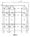
- FIG. 2 illustrates an example of an NOR array of memory cells.
- Memory devices with an NOR type architecture have been implemented with cells of the type illustrated in FIGs. 1B or 1C .
- Each row of memory cells are connected by their sources and drains in a daisy-chain manner. This design is sometimes referred to as a virtual ground design.
- Each memory cell 10 has a source 14, a drain 16, a control gate 30 and a select gate 40.
- the cells in a row have their select gates connected to word line 42.
- the cells in a column have their sources and drains respectively connected to selected bit lines 34 and 36.
- a steering line 36 also connects the control gates of the cells in a column.
- flash EEPROM devices are implemented with memory cells where each is formed with its control gate and select gate connected together. In this case, there is no need for steering lines and a word line simply connects all the control gates and select gates of cells along each row. Examples of these designs are disclosed in United States patent nos. 5,172,338 and 5,418,752 . In these designs, the word line essentially performed two functions: row selection and supplying control gate voltage to all cells in the row for reading or programming.
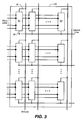
- FIG. 3 illustrates an example of an NAND array of memory cells, such as that shown in FIG. 1D .
- a bit line is coupled to the drain terminal 56 of each NAND cell.
- a source line may connect all their source terminals 54.
- the control gates of the NAND cells along a row are connected to a series of corresponding word lines. An entire row of NAND cells can be addressed by turning on the pair of select transistors (see FIG. 1D ) with appropriate voltages on their control gates via the connected word lines.
- Erase circuits are provided to erase one or more blocks of memory cells.
- a non-volatile memory such as EEPROM is referred to as a "Flash" EEPROM when an entire array of cells, or significant groups of cells of the array, is electrically erased together (i.e., in a flash). Once erased, the group of cells can then be reprogrammed.
- the group of cells erasable together may consist one or more addressable erase unit.
- the erase unit or block typically stores one or more pages of data, the page being the unit of programming and reading, although more than one page may be programmed or read in a single operation.
- Each page typically stores one or more sectors of data, the size of the sector being defined by the host system.
- An example is a sector of 512 bytes of user data, following a standard established with magnetic disk drives, plus some number of bytes of overhead information about the user data and/or the block in with it is stored.
- At least one current breakpoint level is established so as to partition the conduction window into two regions.
- a cell When a cell is read by applying predetermined, fixed voltages, its source/drain current is resolved into a memory state by comparing with the breakpoint level (or reference current I REF ). If the current read is higher than that of the breakpoint level, the cell is determined to be in one logical state (e.g., a "zero" state). On the other hand, if the current is less than that of the breakpoint level, the cell is determined to be in the other logical state (e.g., a "one" state). Thus, such a two-state cell stores one bit of digital information.
- a reference current source which may be externally programmable, is often provided as part of a memory system to generate the breakpoint level current.
- flash EEPROM devices are being fabricated with higher and higher density as the state of the semiconductor technology advances.
- Another method for increasing storage capacity is to have each memory cell store more than two states.
- the conduction window is partitioned into more than two regions by more than one breakpoint such that each cell is capable of storing more than one bit of data.
- the information that a given EEPROM array can store is thus increased with the number of states that each cell can store.
- EEPROM or flash EEPROM with multi-state or multi-level memory cells have been described in U.S. Patent No. 5,172,338 .
- the memory state of a cell is usually read by sensing the conduction current across the source and drain electrodes of the cell when a reference voltage is applied to the control gate.
- a corresponding conduction current with respect to a fixed reference control gate voltage may be detected.
- the range of charge programmable onto the floating gate defines a corresponding threshold voltage window or a corresponding conduction current window.
- the threshold voltage for a given memory state under test is set at the control gate and detect if the conduction current is lower or higher than a threshold current.
- the detection of the conduction current relative to a threshold current is accomplished by examining the rate the conduction current is discharging through the capacitance of the bit line.
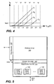
- FIG. 4 illustrates the relation between the source-drain current I D and the control gate voltage V CG for four different charges Q1-Q4 that the floating gate may be selectively storing at any one time.
- the four solid I D versus V CG curves represent four possible charge levels that can be programmed on a floating gate of a memory cell, respectively corresponding to four possible memory states.
- the threshold voltage window of a population of cells may range from 0.5V to 3.5V.
- Six memory states may be demarcated by partitioning the threshold window into five regions in interval of 0.5V each.
- Q4 is in a memory state "5".
- United States Patent No. 4,357,685 discloses a method of programming a 2-state EPROM in which when a cell is programmed to a given state, it is subject to successive programming voltage pulses, each time adding incremental charge to the floating gate. In between pulses, the cell is read back or verified to determine its source-drain current relative to the breakpoint level. Programming stops when the current state has been verified to reach the desired state.
- the programming pulse train used may have increasing period or amplitude.
- Prior art programming circuits simply apply programming pulses to step through the threshold window from the erased or ground state until the target state is reached. Practically, to allow for adequate resolution, each partitioned or demarcated region would require at least about five programming steps to transverse. The performance is acceptable for 2-state memory cells. However, for multi-state cells, the number of steps required increases with the number of partitions and therefore, the programming precision or resolution must be increased. For example, a 16-state cell may require on average at least 40 programming pulses to program to a target state.
- FIG. 5 illustrates schematically a memory device with a typical arrangement of a memory array 100 accessible by read/write circuits 170 via row decoder 130 and column decoder 160.
- a memory transistor of a memory cell in the memory array 100 is addressable via a set of selected word line(s) and bit line(s).
- the row decoder 130 selects one or more word lines and the column decoder 160 selects one or more bit lines in order to apply appropriate voltages to the respective gates of the addressed memory transistor.
- Read/write circuits 170 are provided to read or write (program) the memory states of addressed memory transistors.
- the read/write circuits 170 comprise a number of read/write modules connectable via bit lines to memory elements in the array.
- FIG. 6A is a schematic block diagram of an individual read/write module 190.
- a sense amplifier determines the current flowing through the drain of an addressed memory transistor connected via a selected bit line. The current depends on the charge stored in the memory transistor and its control gate voltage. For example, in a multi-state EEPROM cell, its floating gate can be charged to one of several different levels. For a 4-level cell, it may be used to store two bits of data. The level detected by the sense amplifier is converted by a level-to-bits conversion logic to a set of data bits to be stored in a data latch.
- a logical "page" of memory elements are read or programmed together.
- a row typically contains several interleaved pages. All memory elements of a page will be read or programmed together.
- the column decoder will selectively connect each one of the interleaved pages to a corresponding number of read/write modules.
- the memory array is designed to have a page size of 532 bytes (512 bytes plus 20 bytes of overheads.) If each column contains a drain bit line and there are two interleaved pages per row, this amounts to 8512 columns with each page being associated with 4256 columns.
- the read/write modules forming the read/write circuits 170 can be arranged into various architectures.
- the read/write circuits 170 is organized into banks of read/write stacks 180.
- Each read/write stack 180 is a stack of read/write modules 190.
- the column spacing is determined by the size of the one or two transistors that occupy it.
- the circuitry of a read/write module will likely be implemented with many more transistors and circuit elements and therefore will occupy a space over many columns. In order to service more than one column among the occupied columns, multiple modules are stacked up on top of each other.
- FIG. 6B shows the read/write stack of FIG. 5 implemented conventionally by a stack of read/write modules 190.
- a read/write module may extend over sixteen columns, then a read/write stack 180 with a stack of eight read/write modules can be used to service eight columns in parallel.
- the read/write stack can be coupled via a column decoder to either the eight odd (1,3,5,7,9,11,13,15) columns or the eight even (2, 4, 6, 8, 10, 12, 14, 16) columns among the bank.
- a block decoder is used to multiplex the set of read/write modules to either the even page or the odd page. In this way, whenever one set bit lines are being read or programmed, the interleaving set can be grounded to minimize immediate neighbor coupling.
- the interleaving page architecture is disadvantageous in at least three respects. First, it requires additional multiplexing circuitry. Secondly, it is slow in performance. To finish read or program of memory cells connected by a word line or in a row, two read or two program operations are required. Thirdly, it is also not optimum in addressing other disturb effects such as field coupling between neighboring charge storage elements at the floating gate level when the two neighbors are programmed at different times, such as separately in odd and even pages.
- the problem of neighboring field coupling becomes more pronounced with ever closer spacing between memory transistors.
- a charge storage element is sandwiched between a channel region and a control gate.
- the current that flows in the channel region is a function of the resultant electric field contributed by the field at the control gate and the charge storage element.
- memory transistors With ever increasing density, memory transistors are formed closer and closer together.
- the field from neighboring charge elements then becomes significant contributor to the resultant field of an affected cell.
- the neighboring field depends on the charge programmed into the charge storage elements of the neighbors. This perturbing field is dynamic in nature as it changes with the programmed states of the neighbors. Thus, an affected cell may read differently at different time depending on the changing states of the neighbors.
- the conventional architecture of interleaving page exacerbates the error caused by neighboring floating gate coupling. Since the even page and the odd page are programmed and read independently of each other, a page may be programmed under one set of condition but read back under an entirely different set of condition, depending on what has happened to the intervening page in the meantime.
- the read errors will become more severe with increasing density, requiring a more accurate read operation and coarser partitioning of the threshold window for multi-state implementation. Performance will suffer and the potential capacity in a multi-state implementation is limited.
- United States Patent Publication No. US-2004-0060031-A1 discloses a high performance yet compact non-volatile memory device having a large block of read/write circuits to read and write a corresponding block of memory cells in parallel.
- the memory device has an architecture that reduces redundancy in the block of read/write circuits to a minimum.
- Significant saving in space as well as power is accomplished by redistributing the block of read/write modules into a block read/write module core portions that operate in parallel while interacting with substantially smaller sets of common portions in a time-multiplexing manner.
- data processing among read/write circuits between a plurality of sense amplifiers and data latches is performed by a shared processor.
- Each read/write circuit has a set of data latches for latching input and/or output data of a corresponding one of said group of memory cells.
- the method comprises storing a first, N-bit set of data for a first group of memory cells in N data latches in each of the corresponding sets of data latches and writing the first set of data into said first group of memory cells, wherein the writing includes alternating program and verify phases.
- Each memory cell stores at least N bits of data, where N is greater than one, wherein once the group of memory cells have been programmed past one or more but less than all of the verify levels, one or more of the N data latches in each of the corresponding groups of data latches is released prior to completing said writing.
- the method further comprises transferring a second set of data into the released data latches prior to completing said writing.
- Cache operations are presented that allow data to be transferred in or out of a memory while the internal memory is engaged in another operation, such as a read, program or erase.
- arrangements of data latches and methods of their use are described which allow such cache operations.
- Architectures are described where data latches are shared by a number of physical pages. For example, read/write stacks are associated with the bit lines of the memory, which shared by multiple word lines. While one operation is going on in the memory, if any of these latch are free, they can cache data for future operations in the same or another word line, saving transfer time as this can be hidden behind another operation.
- a cache program operation while programming one page of data another page of data can be loaded in, saving on transfer time.
- a read operation on one word line may be inserted into a write operation on another word line, allowing the data from the read to be transferred out of the memory while the data write continues on.
- Data from another page in the same block, but on a different word line can be toggled out (to, for example, do an ECC operation) while a write or other operation is going on for the first page of data.
- This inter-phase pipelining of operations allows the time needed for the data transfer to be hidden behind the operation on the first page of data.
- this allows a portion of one operation to be inserted between phases of another, typically longer, operation.
- Another example would be to insert a sensing operation between phases of, say, an erase operation, such as before an erase pulse or before a soft programming phase used as the later part of the erase.
- a quicker operation can be interposed in using the shared latches of the read/write stacks if latches available.
- a read can be inserted into a program or erase operation, or a binary program can be inserted into an erase.
- Data can be toggled in and/or out for one page during a program operation for another page that shares the same read write stacks, where, for example, a read of the data to be toggled out and modified is inserted into the verify phase of the data write.
- n such data latches will be needed for each bit line; however, not all of these latches are needed at all times. For example, in a two-bit per cell memory storing data in an upper page/lower page format, one data latches will be needed while programming the lower page (with another latch used if quick pass write is implemented). Two data latches will be needed while programming the upper page (with a third latch used if quick pass write is implemented)). More generally, for memories storing multiple pages, all of the latches will be needed only when programming the highest page. This leaves the other latches available for cache operations.
- latches will free up. Specifically, once only the highest state remains to be verified, only a single latch is needed for verification purposes and the others may be used for cache operations.
- An exemplary embodiment is based on a four state memory storing two-bits per cell and having two latches for data on each bit line and one additional latch for quick pass write.
- the operations of writing the lower page, or erasing, or doing a post erase soft program are basically a binary operation and have one of the data latches free, which can use it to cache data.
- the memory can free up a latch that can be used to cache data.
- An example of how this can be used is that when programming one page, such as in a copy operation, a read of another page that shares the same set of data latches, such as another word line on the same set of bit lines, can be slipped in between program pulse and verifies of the write. The address can then be switched to the page being written, allowing the write process to pick up where it left off without having to restart. While the write continues, the data cached during the interpolated read can be toggled out, checked or modified and transferred back to be present for writing back in once the earlier write operation completes. This sort cache operation allows the toggling out and modification of the second page of data to be hidden behind the programming of the first page.
- FIGs. 1A-1E illustrate schematically different examples of non-volatile memory cells.
- FIG. 2 illustrates an example of an NOR array of memory cells.
- FIG. 3 illustrates an example of an NAND array of memory cells, such as that shown in FIG. 1D .
- FIG. 4 illustrates the relation between the source-drain current and the control gate voltage for four different charges Q1-Q4 that the floating gate may be storing at any one time.
- FIG. 5 illustrates schematically a typical arrangement of a memory array accessible by read/write circuits via row and column decoders.
- FIG. 6A is a schematic block diagram of an individual read/write module.
- FIG. 6B shows the read/write stack of FIG. 5 implemented conventionally by a stack of read/write modules.
- FIG. 7A illustrates schematically a compact memory device having a bank of partitioned read/write stacks.
- FIG. 7B illustrates a preferred arrangement of the compact memory device shown in FIG. 7A .
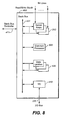
- FIG. 8 illustrates schematically a general arrangement of the basic components in a read/write stack shown in FIG. 7A .
- FIG. 9 illustrates one preferred arrangement of the read/write stacks among the read/write circuits shown in FIGs. 7A and 7B .
- FIG. 10 illustrates an improved embodiment of the common processor shown in FIG 9 .
- FIG. 11A illustrates a preferred embodiment of the input logic of the common processor shown in FIG. 10 .
- FIG. 11B illustrates the truth table of the input logic of FIG. 11A .
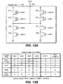
- FIG. 12A illustrates a preferred embodiment of the output logic of the common processor shown in FIG. 10 .
- FIG. 12B illustrates the truth table of the output logic of FIG.12A .
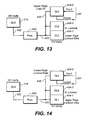
- FIG. 13 is a simplified version of FIG. 10 that shows some specific elements that are relevant to the present discussion in a two-bit embodiment of the present invention
- FIG. 14 indicates the latch assignment for the same elements as FIG. 13 for upper page program where the lower page data is read in.
- FIG.15 illustrates aspects of cache program in the single page mode.
- FIG. 16 shows a programming waveform that can be used in a lower page to full sequence conversion.
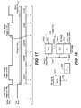
- FIG. 17 illustrates the relative timing in a cache program operation with a full sequence conversion.
- FIG. 18 describes the disposition of latches in a cache page copy operation.
- FIGs. 19A and 19B illustrate the relative timings in cache page copy operations.
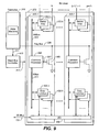
- FIG. 7A illustrates schematically a compact memory device having a bank of partitioned read/write stacks.
- the memory device includes a two-dimensional array of memory cells 300, control circuitry 310, and read/write circuits 370.
- the memory array 300 is addressable by word lines via a row decoder 330 and by bit lines via a column decoder 360.
- the read/write circuits 370 is implemented as a bank of partitioned read/write stacks 400 and allows a block (also referred to as a "page") of memory cells to be read or .programmed in parallel.
- a page is constituted from a contiguous row of memory cells.
- a block multiplexer 350 is provided to multiplex the read/write circuits 370 to the individual blocks.
- the control circuitry 310 cooperates with the read/write circuits 370 to perform memory operations on the memory array 300.
- the control circuitry 310 includes a state machine 312, an on-chip address decoder 314 and a power control module 316.
- the state machine 312 provides chip level control of memory operations.
- the on-chip address decoder 314 provides an address interface between that used by the host or a memory controller to the hardware address used by the decoders 330 and 370.
- the power control module 316 controls the power and voltages supplied to the word lines and bit lines during memory operations.
- FIG. 7B illustrates a preferred arrangement of the compact memory device shown in FIG. 7A .
- Access to the memory array 300 by the various peripheral circuits is implemented in a symmetric fashion, on opposite sides of the array so that access lines and circuitry on each side are reduced in half.
- the row decoder is split into row decoders 330A and 330B and the column decoder into column decoders 360A and 360B.
- the block multiplexer 350 is split into block multiplexers 350A and 350B.
- the read/write circuits are split into read/write circuits 370A connecting to bit lines from the bottom and read/write circuits 370B connecting to bit lines from the top of the array300. In this way, the density of the read/write modules, and therefore that of the partitioned read/write stacks 400, is essentially reduced by one half.
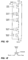
- FIG. 8 illustrates schematically a general arrangement of the basic components in a read/write tack shown in FIG. 7A .
- the read/write stack 400 comprises a stack of sense amplifiers 212 for sensing k bit lines, an I/O module 440 for input or output of data via an I/O bus 231, a stack of data latches 430 for storing input or output data, a common processor 500 to process and store data among the read/write stack 400, and a stack bus 421 for communication among the stack components.
- a stack bus controller among the read/write circuits 370 provides control and timing signals via lines 411 for controlling the various components among the read/write stacks.
- FIG. 9 illustrates one preferred arrangement of the read/write stacks among the read/write circuits shown in FIGs. 7A and 7B .
- the entire bank of partitioned read/write stacks 400 operating in parallel allows a block (or page) of p cells along a row to be read or programmed in parallel.
- p p/k.
- the block is a run of the entire row of cells.
- the block is a subset of cells in the row.
- the subset of cells could be one half of the entire row or one quarter of the entire row.
- the subset of cells could be a run of contiguous cells or one every other cell, or one every predetermined number of cells.
- Each read/write stack such as 400-1, essentially contains a stack of sense amplifiers 212-1 to 212-k servicing a segment of k memory cells in parallel.
- a preferred sense amplifier is disclosed in United States Patent Publication No. 2004-0109357-A1 .
- the stack bus controller 410 provides control and timing signals to the read/write circuit 370 via lines 411.
- the stack bus controller is itself dependent on the memory controller 310 via lines 311. Communication among each read/write stack 400 is effected by an interconnecting stack bus 431 and controlled by the stack bus controller 410.
- Control lines 411 provide control and clock signals from the stack bus controller 410 to the components of the read/write stacks 400-1.
- the stack bus is partitioned into a SABus 422 for communication between the common processor 500 and the stack of sense amplifiers 212, and a DBus 423 for communication between the processor and the stack of data latches 430.
- the stack of data latches 430 comprises of data latches 430-1 to 430-k, one for each memory cell associated with the stack
- the I/O module 440 enables the data latches to exchange data with the external via an I/O bus 231.
- the common processor also includes an output 507 for output of a status signal indicating a status of the memory operation, such as an error condition.
- the status signal is used to drive the gate of an n-transistor 550 that is tied to a FLAG BUS 509 in a Wired Or configuration.
- the FLAG BUS is preferably precharged by the controller 310 and will be pulled down when a status signal is asserted by any of the read/write stacks.
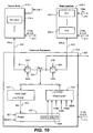
- FIG. 10 illustrates an improvement of the common processor shown in FIG 9 .
- the common processor 500 comprises a processor bus, PBUS 505 for communication with external circuits, an input logic 510, a processor latch PLatch 520 and an output logic 530.
- the input logic 510 receives data from the PBUS and outputs to a BSI node as a transformed data in one of logical states "1", “0", or “Z” (float) depending on the control signals from the stack bus controller 410 via signal lines 411.
- a Set/Reset latch, PLatch 520 then latches BSI, resulting in a pair of complementary output signals as MTCH and MTCH*.
- the output logic 530 receives the MTCH and MTCH* signals and outputs on the PBUS 505 a transformed data in one of logical states "1", “0", or "Z" (float) depending on the control signals from the stack bus controller 410 via signal lines 411.
- FIG. 10 illustrates the case for the memory cell coupled to bit line 1.
- the corresponding sense amplifier 212-1 comprises a node where the sense amplifier data appears.
- the node assumes the form of a SA Latch, 214-1 that stores data.
- the corresponding set of data latches 430-1 stores input or output data associated with the memory cell coupled to bit line 1.
- the set of data latches 430-1 comprises sufficient data latches, 434-1, ..., 434-n for storing n-bits of data.
- the PBUS 505 of the common processor 500 has access to the SA latch 214-1 via the SBUS 422 when a transfer gate 501 is enabled by a pair of complementary signals SAP and SAN. Similarly, the PBUS 505 has access to the set of data latches 430-1 via the DBUS 423 when a transfer gate 502 is enabled by a pair of complementary signals DTP and DTN.
- the signals SAP, SAN, DTP and DTN are illustrated explicitly as part of the control signals from the stack bus controller 410.
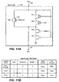
- FIG. 11A illustrates a preferred embodiment of the input logic of the common processor shown in FIG. 10 .
- the input logic 520 receives the data on the PBUS 505 and depending on the control signals, either has the output BSI being the same, or inverted, or floated.
- the output BSI node is essentially affected by either the output of a transfer gate 522 or a pull-up circuit comprising p-transistors 524 and 525 in series to Vdd, or a pull-down circuit comprising n-transistors 526 and 527 in series to ground.
- the pull-up circuit has the gates to the p-transistor 524 and 525 respectively controlled by the signals PBUS and ONE.
- the pull-down circuit has the gates to the n-transistors 526 and 527 respectively controlled by the signals ONEB ⁇ 1> and PBUS.
- FIG. 11B illustrates the truth table of the input logic of FIG. 11A .
- the logic is controlled by PBUS and the control signals ONE, ONEB ⁇ 0>, ONEB ⁇ 1> which are part of the control signals from the stack bus controller 410.
- PBUS control signals
- ONE, ONEB ⁇ 0>, ONEB ⁇ 1> which are part of the control signals from the stack bus controller 410.
- three transfer modes, PASSTHROUGH, INVERTED, and FLOATED are supported.
- the signals ONE is at a logical "1", ONEB ⁇ 0> at "0" and ONEB ⁇ 1> at "0". This will disable the pull-up or pull-down but enable the transfer gate 522 to pass the data on the PBUS 505 to the output 523.
- the signals ONE is at "0", ONEB ⁇ 0> at "1” and ONE ⁇ 1> at "1”. This will disable the transfer gate 522.
- the pull-down circuit will be disabled while the pull-up circuit is enabled, resulting in BSI being at "1".
- the output BSI can be floated by having the signals ONE at "1", ONE ⁇ 0> at "1” and ONEB ⁇ 1> at "0".
- the FLOATED mode is listed for completeness although in practice, it is not used.
- FIG. 12A illustrates a preferred embodiment of the output logic of the common processor shown in FIG. 10 .
- the signal at the BSI node from the input logic 520 is latched in the processor latch, PLatch 520.
- the output logic 530 receives the data MTCH and MTCH* from the output of PLatch 520 and depending on the control signals, outputs on the PBUS as either in a PASSTHROUGH, INVERTED OR FLOATED mode.
- the four branches act as drivers for the PBUS 505, actively pulling it either to a HIGH, LOW or FLOATED state. This is accomplished by four branch circuits, namely two pull-up and two pull-down circuits for the PBUS 505.
- a first pull-up circuit comprises p-transistors 531 and 532 in series to Vdd, and is able to pull up the PBUS when MTCH is at "0".
- a second pull-up circuit comprises p-transistors 533 and 534 in series to ground and is able to pull up the PBUS when MTCH is at "1".
- a first pull-down circuit comprises n-transistors 535 and 536 in series to Vdd, and is able to pull down the PBUS when MTCH is at "0".
- a second pull-up circuit comprises n-transistors 537 and 538 in series to ground and is able to pull up the PBUS when MTCH is at "1".
- One feature of the arrangement is to constitute the pull-up circuits with PMOS transistors and the pull-down circuits with NMOS transistors. Since the pull by the NMOS is much stronger than that of the PMOS, the pull-down will always overcome the pull-up in any contentions. In other words, the node or bus can always default to a pull-up or "1" state, and if desired, can always be flipped to a "0" state by a pull-down.
- FIG. 12B illustrates the truth table of the output logic of FIG. 12A .
- the logic is controlled by MTCH, MTCH* latched from the input logic and the control signals PDIR, PINV, NDIR, NINV, which are part of the control signals from the stack bus controller 410.
- Four operation modes, PASSTHROUGH, INVERTED, FLOATED, and PRECHARGE are supported.
- a number of aspects of the present invention make use of the data latches of the read/write stacks described above in FIG. 10 for cache operations that will data in and out while the internal memory is doing other operations such as read, write, or erase.
- data latches are shared by a number of physical pages. For example, as on the read/write stacks of the bit lines, shared by all of the word lines, so while one operation is going on, if any of these latches are free, they can cache data for future operations in the same or another word line, saving transfer time as this can be hidden behind another operation. This can improve performance by increasing the amount of pipelining of different operations or phases of operations.
- a read operation on one word line is inserted into a write operation on another word line, allowing the data from the read to be transferred out of the memory while the data write continues on.
- this allows data from another page in the same block, but on a different word line, to be toggled out (to, for example, do an ECC operation) while the write or other operation is going on for the first page of data.
- This inter-phase pipelining of operations allows the time needed for the data transfer to be hidden behind the operation on the first page of data. More generally, this allows a portion of one operation to be inserted between phases of another, typically longer, operation. Another example would be to insert a sensing operation between phases of, say, an erase operation, such as before an erase pulse or before a soft programming phase used as the later part of the erase.
- a set of exemplary time values for the system described above can be take as:
- n such data latches will be needed for each bit line; however, not all of these latches are needed at all times. For example, in a two-bit per cell memory storing data in an upper page/lower page format, two data latches will be needed while programming the lower page. More generally, for memories storing multiple pages, all of the latches will be needed only when programming the highest page. This leaves the other latches available for cache operations. Further, even while writing the highest page, as the various states are removed from the verify phase of the write operation, latches will free up. Specifically, once only the highest state remains to be verified, only a single latch is needed for verification purposes and the others may be used for cache operations.
- An example of how this can be used is that when programming one page, such as in a copy operation, a read of another page that shares the same set of data latches, such as another word line on the same set of bit lines, can be slipped in during the verify phase of the write. The address can then be switched to the page being written, allowing the write process to pick up where it left off without having to restart. While the write continues, the data cached during the interpolated read can be toggled out, checked or modified and transferred back to be present for writing back in once the earlier write operation completes. This sort cache operation allows the toggling out and modification of the second page of data to be hidden behind the programming of the first page.
- FIG. 13 is a simplified version of FIG. 10 that shows some specific elements that are relevant to the present discussion in a two-bit embodiment, the other elements being suppressed to simplify the discussion. These include data latch DL0 434-0, which is connected Data I/O line 231, data latch DL1 434-1, connected to common processor 500 by line 423, data latch DL2 434-2, commonly connected with the other data latches by line 435, and sense amp data latch DLS 214, which is connected to common processor 500 by line 422.
- the various elements of FIG. 13 are labeled according to their disposition during the programming of the lower page.
- the latch DL2 434-2 is used for the lower verify (VL) in quick pass write mode, as is described in U.S. patent application entitled “Use of Data Latches in Multi-Phase Programming of Non-Volatile Memories” filed concurrently with the present application; the inclusion of the register, and of using quick pass write when it is included, are optional, but the exemplary embodiment will include this register.
- the programming of the lower page can include the following steps:
- FIG. 14 shows the same elements as FIG. 13 , but indicates the latch assignment for upper page program where the lower page data is read in. (The description again uses conventional coding, so that the programming of the upper page is to the B and C states.)
- the programming of the upper page can include the following steps:
- step 6 the latch DL0 434-0 is no longer required and can be used to cache data for the next programming operation. Additionally, in embodiments using quick pass write, once the second, slowly programming phase is entered, the latch DL2 434-2 could also be made available for caching data, although, in practice, it is often the case that this is only available in this way for a fairly short time period that does not justify the additional overhead that is often required to implement this feature.
- FIG. 15 can be used to illustrate many of the aspects of cache program in the single page mode that has been described in the last few paragraphs.
- FIG. 15 shows the relative timing of what events are occurring internally to the memory (the lower "True Busy” line) and as seen from external to the memory (the upper "Cache Busy” line).
- the lower page to be programmed onto the selected word line (WLn) is loaded into the memory. This assumes the first lower page of data has not been previously cached, as it will be for the subsequent pages.
- the lower page is finished loading and the memory begins to write it. Since this is equivalent to a binary operation at this point, only the state A needs to be verified ("pvfyA") and the data latch DL0 434-0 is available to receive the next page of data, here taken as the upper pages to be programmed into WLn, at time t 2 , which is consequently cached in latch DL0 434-0 during the programming of the lower page.
- the programming of the upper page begins at time t 4 , where initially only the B state is verified ("pvfyB”), the C state being added at t 5 (“pvfyB/C"). Once the B state is no longer being verified at t 6 , only the C state needs to be verified (“pvfyC”) and the latch DL0 434-0 is freed up. This allows the next data set to be cached while the upper page finishes programming.
- steps (1)-(4) are as for the lower page process in single page program mode:
- FIG. 17 is a schematic representation of the relative times involved in the lower page to full sequence conversion write process.
- the process is as described above for the process in FIG. 15 .
- the verification process is switched to include the B states with the A states. Once all of the A states lock out, the verify process switches to checking for the B and C states at time t 4 .
- the B states Once the B states have verified at t 5 , only the C state needs to be checked and a register can be freed up to load the next data to be programmed, such as the lower page on the next word line (WL n+1 ) as indicated on the Cache Busy line.
- this next data set has been cached and one the programming of the C data for the previous set concludes at t 7 , this next data set begins programming. Additionally, while the (here) lower page on word line WL n+1 is programming, the next data (such as the corresponding upper page data) can be loaded into the open latch DL0 434-0.
- a status report is implemented in a way that gives lower page and upper page status independently.
- a scan of physical page can be performed.
- a first scan can check latch DL0 434-0 for unfinished upper page data
- a second scan can check DL1 434-1 for unfinished lower page data. Since, the verification of the B state will change both DL0 434-0 and DL1 434-1 data, an A state verification should be performed in the way that DL1 434-1 data "0" will be changed to "1" if the bit's threshold value is higher than the A verify level.
- This post verify will check on whether any under programmed B levels are passing at the A level; if they are passing at the A level, then the error is only on upper page and not on lower page; if they are not passing at the A level, then both lower and upper pages have error.
- the C state will be transferred to latch DL1 434-1 to finish programming. In this case, the scan of latch is not necessary for lower page, because the lower page will have already passed program without any failed bits.
- Another set of exemplary embodiments of the present invention relate to page copy operations, where a data set is relocated from one location to another.
- Various aspects of data relocation operations are described in U.S. patent applications number US 10/846,289, filed May 13, 2004 (published as US 2005-0257120A1 ); number 11/022,462, December 21, 2004 (published as US 2006-0136687A1 ); and number US 10/915,039, filed August 9, 2004 (published as US 2006-0031593A1 ); and U.S. patent number 6,266,273 .
- the data is often toggled out to be checked (for error, for example), updated (such as updating a header), or both (such correcting detected error).
- a principal aspect of the present invention allows for a data read to an open register to be interpolated during the verify phase of a write operation, with this cached data then being transferred out of the memory device as the write operation continues, allowing the time for toggling the data out to hide behind the write operation.
- FIG. 18 indicates the disposition of the exemplary arrangement of latches as the process progresses.
- the first version of cache page copy will write to a lower page and can include the following steps, where read addresses are labeled M, M+1, ..., and write addresses are labeled N, N+1, ..:
- the program/verify process can be paused to insert a read operation and then restart the write operation, picking up at the point where it left off.
- the data that was read during this interleaved sensing operation can then be toggled out while the resumed write operation continues on.
- this second process allows for the page copy mechanism to be used in an upper page or full sequence write process once only the C state is being verified and one latch on each bit line opens up.
- the second cache page copy operation begins with the same first three steps as in the first case, but then differs. It can include the following steps:
- FIGs. 19A and 19B illustrate the relative timing of the second cache page copy method, where FIG. 19B illustrates the algorithm with the full sequence write conversion and FIG. 19A illustrates the algorithm without.
- FIG. 19A and 19B are composed of two parts, the first, upper part beginning at the broken vertical line A, corresponding to t 0 , and ending with the broken vertical line B, corresponding to t 5 ; the second, lower part is a continuation of the upper portion and begins with the broken vertical line B, corresponding to t 5 .
- the line B at time t 5 is same in the upper portion as in the lower portion, being just a seam in two parts allowing it to be displayed on two lines.
- FIG. 19A shows a process that starts with reading of a first page (page M) that is taken to be a lower page in this example, assumes no data has previously been cached, and operates in single page mode, waiting until the lower page has finished writing before beginning to write the upper page.
- the process starts at time to with a read of the page M (Sense page M (L)), which here is a lower that is sensed by a read at the A and C levels in this coding.
- Sense page M (L) is a lower that is sensed by a read at the A and C levels in this coding.
- the read is complete and page M can be toggled out and checked or modified.
- a next page here page M+1, the upper page corresponding to the same physical as lower page M
- a process that finishes at time t 3 .
- the first page (originating from Page M) (lower) is ready to be programmed back into the memory at page N and the data read from page M+1 is being held in a latch and can be transferred out to be modified/checked. Both of these processes can start at the same time, here t 3 .
- the data from page M+1 has been toggled out and modified by time t 4 ; however, for the embodiment not implementing a full sequence conversion, the memory will wait until page N finishes at time t 5 to begin writing the second read page of data (originating from Page M+1) into page N+1.
- page N+1 is an upper page
- its write begins initially with a verification at the B level, the C level being added at t 6 .
- the B state verification is dropped. As described above this allows a data latch to be freed up, an ongoing write operation is suspended, a reading operation (at a different address than the suspended program/verify operation) is interposed, the write then resumes where it left off, and the data sensed the interposed write operation can be toggled out while the resumed write operation runs on.
- the interposed write operation is performed for the, here, lower page M+2.
- This sensing is finished at time t 8 and the write of page N+1 picks back up and the data from page M+2 is concurrently toggled out and modified.
- page N+1 finishes programming at time t 9 before page M+2 is finished at time t 10 .
- a write of the data originating from page M+2 could begin; however, in this embodiment, instead a read of page M+3 is first executed, allowing for this page's data to be toggled out and the modification to be hidden behind the writing of the data originating from page M+2 into page N+2, beginning at time t 11 .
- the process then continues on as in the earlier parts of the diagram, but with the page numbers shifted, with time t 11 corresponding to time t 3 , time t 12 corresponding to time t 4 , and so on until the copy process is stopped.
- FIG. 19B again shows a process that starts with reading of a lower page, page M that is taken to be a lower page, and assumes no data has previously been cached.
- FIG. 19B differs from FIG. 19A by implementing a conversion to full sequence write at time t 4 . This roughly speeds up the process by the time ( t 5 -t 4 ) of FIG. 19A .
- the various changes related to the full sequence conversion are implemented as described previously. Otherwise, the process is similar to that of FIG. 19A , including those aspects found between times t 7 and t 12 .
- the write process can begin verifying only the A level. After ever A verify, it is checked to see wether any bits have passed. If so, the B level can be added to the verify phase. The A level verify will be removed after all storage units with it as their target values verify (or except a maximum count based on a settable parameter). Similarly, after the verifications at the B level, a verify of the C level can be added, with the B level verify being removed after all storage units with it as their target values verify (or except a maximum count based on a settable parameter).
Landscapes
- Engineering & Computer Science (AREA)
- Theoretical Computer Science (AREA)
- Physics & Mathematics (AREA)
- General Engineering & Computer Science (AREA)
- General Physics & Mathematics (AREA)
- Microelectronics & Electronic Packaging (AREA)
- Read Only Memory (AREA)
- Memory System Of A Hierarchy Structure (AREA)
- Non-Volatile Memory (AREA)
Claims (4)
- Procédé pour exploiter un dispositif de mémoire non-volatile lequel inclut une matrice de cellules de mémoire (300) et un ensemble de circuits de lecture/écriture (370' 370a; 370b) destiné à être exploités sur un groupe de cellules de mémoire de ladite matrice en parallèle, chaque circuit de lecture/écriture (370' 370a; 370b) présentant un ensemble de verrous de données (430, 430-I ..., 430-k) pour verrouiller des données d'entrée et/ou des données de sortie de l'un correspondant dudit groupe de cellules de mémoire, le procédé comprenant les étapes ci-après consistant à :stocker un premier ensemble de données de N bits pour un premier groupe de cellules de mémoire dans N verrous de données, dans chacun des ensembles de verrous de données correspondants (430, 430-I, ... 430-k); etécrire le premier ensemble de données dans ledit premier groupe de cellules de mémoire, dans lequel l'écriture comprend des phases alternées de vérification et de programmation;caractérisé en ce quechaque cellule de mémoire stocke au moins N bits de données, où N est un nombre supérieur à un ;dans lequel, une fois le groupe de cellules de mémoire a été programmé suite à un ou plusieurs niveaux de vérification, mais moins que la totalité de ces niveaux de vérification, un ou plusieurs des N verrous de données dans chacun des groupes de verrous de données correspondants (430, 430-I, ... 430-k) est/sont libéré(s) avant d'achever ladite écriture, et en ce qu'il comporte l'étape consistant àtransférer un second ensemble de données dans les verrous de données libérés avant d'achever ladite écriture.
- Procédé selon la revendication 1, dans lequel ledit second ensemble de données est destiné à un second groupe de cellules de mémoire de la matrice sur laquelle l'ensemble de circuits de lecture/écriture (370' 370a ; 370b) est en mesure d'opérer, dans lequel le second groupe de cellules de mémoire est différent du premier groupe de cellules de mémoire.
- Procédé selon la revendication 1, dans lequel ladite étape de transfert comporte l'étape consistant à lire ledit second ensemble de données à partir dudit second groupe de cellules de mémoire dans les verrous libérés, dans lequel ladite étape de lecture est mise en oeuvre entre les impulsions de ladite écriture.
- Procédé selon la revendication 1, dans lequel ladite étape de transfert comporte l'étape consistant à transférer ledit second ensemble de données hors des verrous libérés, dans lequel ledit transfert est initié avant d'achever ladite écriture.
Applications Claiming Priority (2)
| Application Number | Priority Date | Filing Date | Title |
|---|---|---|---|
| US11/097,590 US7206230B2 (en) | 2005-04-01 | 2005-04-01 | Use of data latches in cache operations of non-volatile memories |
| PCT/US2006/011248 WO2006107654A1 (fr) | 2005-04-01 | 2006-03-27 | Utilisation de verrous de donnees dans des operations de cache de memoire non volatile |
Publications (2)
| Publication Number | Publication Date |
|---|---|
| EP1864289A1 EP1864289A1 (fr) | 2007-12-12 |
| EP1864289B1 true EP1864289B1 (fr) | 2010-02-17 |
Family
ID=36636435
Family Applications (1)
| Application Number | Title | Priority Date | Filing Date |
|---|---|---|---|
| EP06739812A Not-in-force EP1864289B1 (fr) | 2005-04-01 | 2006-03-27 | Utilisation de verrous de donnees dans des operations de cache de memoire non volatile |
Country Status (9)
| Country | Link |
|---|---|
| US (13) | US7206230B2 (fr) |
| EP (1) | EP1864289B1 (fr) |
| JP (1) | JP5038292B2 (fr) |
| KR (1) | KR101106977B1 (fr) |
| CN (1) | CN101171641B (fr) |
| AT (1) | ATE458248T1 (fr) |
| DE (1) | DE602006012293D1 (fr) |
| TW (1) | TWI396199B (fr) |
| WO (1) | WO2006107654A1 (fr) |
Families Citing this family (288)
| Publication number | Priority date | Publication date | Assignee | Title |
|---|---|---|---|---|
| US5657332A (en) | 1992-05-20 | 1997-08-12 | Sandisk Corporation | Soft errors handling in EEPROM devices |
| US7012835B2 (en) | 2003-10-03 | 2006-03-14 | Sandisk Corporation | Flash memory data correction and scrub techniques |
| US7490283B2 (en) | 2004-05-13 | 2009-02-10 | Sandisk Corporation | Pipelined data relocation and improved chip architectures |
| KR101051703B1 (ko) | 2004-08-09 | 2011-07-25 | 삼성전자주식회사 | 서스펜드/리쥼 기능을 갖는 집적 회로 카드 및 집적 회로카드 시스템 |
| US7158421B2 (en) * | 2005-04-01 | 2007-01-02 | Sandisk Corporation | Use of data latches in multi-phase programming of non-volatile memories |
| US7849381B2 (en) | 2004-12-21 | 2010-12-07 | Sandisk Corporation | Method for copying data in reprogrammable non-volatile memory |
| US7251160B2 (en) * | 2005-03-16 | 2007-07-31 | Sandisk Corporation | Non-volatile memory and method with power-saving read and program-verify operations |
| US7206230B2 (en) * | 2005-04-01 | 2007-04-17 | Sandisk Corporation | Use of data latches in cache operations of non-volatile memories |
| US7463521B2 (en) | 2005-04-01 | 2008-12-09 | Sandisk Corporation | Method for non-volatile memory with managed execution of cached data |
| US7447078B2 (en) * | 2005-04-01 | 2008-11-04 | Sandisk Corporation | Method for non-volatile memory with background data latch caching during read operations |
| US7564713B2 (en) * | 2005-04-28 | 2009-07-21 | Kabushiki Kaisha Toshiba | Semiconductor integrated circuit device wherein during data write a potential transferred to each bit line is changed in accordance with program order of program data |
| EP1750278B1 (fr) * | 2005-07-28 | 2009-11-11 | STMicroelectronics S.r.l. | Procédé de programmation d'un dispositif de mémoire instantanée à quatre états et tampon de page correspondant |
| JP5162846B2 (ja) * | 2005-07-29 | 2013-03-13 | ソニー株式会社 | 記憶装置、コンピュータシステム、および記憶システム |
| US20100302919A1 (en) * | 2005-10-27 | 2010-12-02 | Mediatek Inc. | Optical Recording Method and Apparatus |
| EP1850347A1 (fr) * | 2006-04-28 | 2007-10-31 | Deutsche Thomson-Brandt Gmbh | Procédé et dispositif d'écriture pour la mémoire instantanée |
| US7917685B2 (en) * | 2006-05-04 | 2011-03-29 | Micron Technology, Inc. | Method for reading a multilevel cell in a non-volatile memory device |
| WO2007131059A2 (fr) * | 2006-05-05 | 2007-11-15 | Sandisk Corporation | Mémoire non volatile à mise en antémémoire des verrous des données en arrière-plan pendant les opérations d'effacement, et procédés à cet effet |
| WO2007130976A2 (fr) * | 2006-05-05 | 2007-11-15 | Sandisk Corporation | Mémoire non volatile disposant de mise en antémémoire de verrous de données d'arrière plan lors d'exploitations de programmeset procédés associés |
| US7355892B2 (en) * | 2006-06-30 | 2008-04-08 | Sandisk Corporation | Partial page fail bit detection in flash memory devices |
| US7885112B2 (en) | 2007-09-07 | 2011-02-08 | Sandisk Corporation | Nonvolatile memory and method for on-chip pseudo-randomization of data within a page and between pages |
| US7734861B2 (en) | 2006-09-08 | 2010-06-08 | Sandisk Corporation | Pseudo random and command driven bit compensation for the cycling effects in flash memory |
| US7606966B2 (en) * | 2006-09-08 | 2009-10-20 | Sandisk Corporation | Methods in a pseudo random and command driven bit compensation for the cycling effects in flash memory |
| US7716538B2 (en) * | 2006-09-27 | 2010-05-11 | Sandisk Corporation | Memory with cell population distribution assisted read margining |
| US7886204B2 (en) | 2006-09-27 | 2011-02-08 | Sandisk Corporation | Methods of cell population distribution assisted read margining |
| US7747813B2 (en) * | 2006-11-24 | 2010-06-29 | Sandforce, Inc. | Multi-memory device system and method for managing a lifetime thereof |
| US7904619B2 (en) | 2006-11-24 | 2011-03-08 | Sandforce, Inc. | System, method, and computer program product for reducing memory write operations using difference information |
| US7809900B2 (en) * | 2006-11-24 | 2010-10-05 | Sandforce, Inc. | System, method, and computer program product for delaying an operation that reduces a lifetime of memory |
| US7904672B2 (en) | 2006-12-08 | 2011-03-08 | Sandforce, Inc. | System and method for providing data redundancy after reducing memory writes |
| US7616506B2 (en) * | 2006-12-28 | 2009-11-10 | Sandisk Corporation | Systems for complete word line look ahead with efficient data latch assignment in non-volatile memory read operations |
| US7616505B2 (en) * | 2006-12-28 | 2009-11-10 | Sandisk Corporation | Complete word line look ahead with efficient data latch assignment in non-volatile memory read operations |
| US7499320B2 (en) * | 2007-03-07 | 2009-03-03 | Sandisk Corporation | Non-volatile memory with cache page copy |
| US7502255B2 (en) * | 2007-03-07 | 2009-03-10 | Sandisk Corporation | Method for cache page copy in a non-volatile memory |
| KR100813631B1 (ko) * | 2007-03-19 | 2008-03-14 | 삼성전자주식회사 | 읽기 성능을 향상시킬 수 있는 플래시 메모리 장치 |
| US7573773B2 (en) * | 2007-03-28 | 2009-08-11 | Sandisk Corporation | Flash memory with data refresh triggered by controlled scrub data reads |
| US7477547B2 (en) | 2007-03-28 | 2009-01-13 | Sandisk Corporation | Flash memory refresh techniques triggered by controlled scrub data reads |
| US7606071B2 (en) * | 2007-04-24 | 2009-10-20 | Sandisk Corporation | Compensating source voltage drop in non-volatile storage |
| US7606072B2 (en) * | 2007-04-24 | 2009-10-20 | Sandisk Corporation | Non-volatile storage with compensation for source voltage drop |
| KR100927119B1 (ko) * | 2007-05-10 | 2009-11-18 | 삼성전자주식회사 | 불 휘발성 반도체 메모리 장치 및 그것의 프로그램 방법 |
| JP2008310841A (ja) * | 2007-06-12 | 2008-12-25 | Panasonic Corp | 半導体記憶装置及び電子装置 |
| WO2009095902A2 (fr) | 2008-01-31 | 2009-08-06 | Densbits Technologies Ltd. | Systèmes et procédés pour traiter des erreurs de données immédiates dans une mémoire flash |
| US8694715B2 (en) | 2007-10-22 | 2014-04-08 | Densbits Technologies Ltd. | Methods for adaptively programming flash memory devices and flash memory systems incorporating same |
| US7903486B2 (en) * | 2007-11-19 | 2011-03-08 | Sandforce, Inc. | System, method, and computer program product for increasing a lifetime of a plurality of blocks of memory |
| US7849275B2 (en) | 2007-11-19 | 2010-12-07 | Sandforce, Inc. | System, method and a computer program product for writing data to different storage devices based on write frequency |
| US8453022B2 (en) | 2007-12-05 | 2013-05-28 | Densbits Technologies Ltd. | Apparatus and methods for generating row-specific reading thresholds in flash memory |
| WO2009074978A2 (fr) | 2007-12-12 | 2009-06-18 | Densbits Technologies Ltd. | Systèmes et procédés pour une correction d'erreurs et un décodage sur des milieux physiques à multiples niveaux |
| US8307180B2 (en) | 2008-02-28 | 2012-11-06 | Nokia Corporation | Extended utilization area for a memory device |
| US7986554B2 (en) | 2008-03-19 | 2011-07-26 | Sandisk Technologies Inc. | Different combinations of wordline order and look-ahead read to improve non-volatile memory performance |
| US7961512B2 (en) * | 2008-03-19 | 2011-06-14 | Sandisk Corporation | Adaptive algorithm in cache operation with dynamic data latch requirements |
| WO2009118720A2 (fr) | 2008-03-25 | 2009-10-01 | Densbits Technologies Ltd. | Appareil et procédés pour l’arrondi non biaisé à efficacité matérielle |
| CN102027455A (zh) | 2008-05-13 | 2011-04-20 | 拉姆伯斯公司 | 用于存储器器件的分式编程命令 |
| US8130576B2 (en) * | 2008-06-30 | 2012-03-06 | Intel Corporation | Memory throughput increase via fine granularity of precharge management |
| US7729166B2 (en) * | 2008-07-02 | 2010-06-01 | Mosaid Technologies Incorporated | Multiple-bit per cell (MBC) non-volatile memory apparatus and system having polarity control and method of programming same |
| KR101395152B1 (ko) * | 2008-07-18 | 2014-05-15 | 삼성전자주식회사 | 비휘발성 메모리 셀, 비휘발성 메모리 장치 및 상기비휘발성 메모리 장치의 프로그래밍 방법 |
| US7852671B2 (en) * | 2008-10-30 | 2010-12-14 | Micron Technology, Inc. | Data path for multi-level cell memory, methods for storing and methods for utilizing a memory array |
| CN102246240A (zh) * | 2008-12-09 | 2011-11-16 | 拉姆伯斯公司 | 用于并发和流水线存储器操作的非易失性存储器器件 |
| US8819385B2 (en) | 2009-04-06 | 2014-08-26 | Densbits Technologies Ltd. | Device and method for managing a flash memory |
| US8458574B2 (en) | 2009-04-06 | 2013-06-04 | Densbits Technologies Ltd. | Compact chien-search based decoding apparatus and method |
| US8832353B2 (en) * | 2009-04-07 | 2014-09-09 | Sandisk Technologies Inc. | Host stop-transmission handling |
| JP5532671B2 (ja) * | 2009-05-08 | 2014-06-25 | ソニー株式会社 | データ記憶システムおよびデータ記憶方法、実行装置および制御方法、並びに制御装置および制御方法 |
| US8874824B2 (en) | 2009-06-04 | 2014-10-28 | Memory Technologies, LLC | Apparatus and method to share host system RAM with mass storage memory RAM |
| US8027195B2 (en) * | 2009-06-05 | 2011-09-27 | SanDisk Technologies, Inc. | Folding data stored in binary format into multi-state format within non-volatile memory devices |
| US8102705B2 (en) | 2009-06-05 | 2012-01-24 | Sandisk Technologies Inc. | Structure and method for shuffling data within non-volatile memory devices |
| US8132045B2 (en) * | 2009-06-16 | 2012-03-06 | SanDisk Technologies, Inc. | Program failure handling in nonvolatile memory |
| US8307241B2 (en) * | 2009-06-16 | 2012-11-06 | Sandisk Technologies Inc. | Data recovery in multi-level cell nonvolatile memory |
| US20110002169A1 (en) | 2009-07-06 | 2011-01-06 | Yan Li | Bad Column Management with Bit Information in Non-Volatile Memory Systems |
| US8180994B2 (en) | 2009-07-08 | 2012-05-15 | Sandisk Technologies Inc. | Optimized page programming order for non-volatile memory |
| WO2011010184A1 (fr) | 2009-07-20 | 2011-01-27 | Freescale Semiconductor, Inc. | Système de traitement de signal, circuit intégré comprenant une logique de commande de mémoire tampon et procédé pour ce système |
| US8516166B2 (en) * | 2009-07-20 | 2013-08-20 | Lsi Corporation | System, method, and computer program product for reducing a rate of data transfer to at least a portion of memory |
| JP5316299B2 (ja) * | 2009-08-07 | 2013-10-16 | 富士通セミコンダクター株式会社 | 半導体メモリ、システムおよび半導体メモリの動作方法 |
| US9330767B1 (en) | 2009-08-26 | 2016-05-03 | Avago Technologies General Ip (Singapore) Pte. Ltd. | Flash memory module and method for programming a page of flash memory cells |
| US8995197B1 (en) | 2009-08-26 | 2015-03-31 | Densbits Technologies Ltd. | System and methods for dynamic erase and program control for flash memory device memories |
| US8730729B2 (en) | 2009-10-15 | 2014-05-20 | Densbits Technologies Ltd. | Systems and methods for averaging error rates in non-volatile devices and storage systems |
| US8724387B2 (en) | 2009-10-22 | 2014-05-13 | Densbits Technologies Ltd. | Method, system, and computer readable medium for reading and programming flash memory cells using multiple bias voltages |
| KR101893332B1 (ko) * | 2009-11-13 | 2018-08-31 | 가부시키가이샤 한도오따이 에네루기 켄큐쇼 | 반도체 장치 및 반도체 장치의 구동 방법 |
| KR101636248B1 (ko) * | 2009-12-10 | 2016-07-06 | 삼성전자주식회사 | 플래시 메모리 장치, 이를 포함하는 플래시 메모리 시스템 및 이의 프로그램 방법 |
| US8213243B2 (en) * | 2009-12-15 | 2012-07-03 | Sandisk 3D Llc | Program cycle skip |
| JP2011129176A (ja) * | 2009-12-15 | 2011-06-30 | Toshiba Corp | 不揮発性半導体記憶装置 |
| US8468294B2 (en) * | 2009-12-18 | 2013-06-18 | Sandisk Technologies Inc. | Non-volatile memory with multi-gear control using on-chip folding of data |
| US8725935B2 (en) | 2009-12-18 | 2014-05-13 | Sandisk Technologies Inc. | Balanced performance for on-chip folding of non-volatile memories |
| US9092340B2 (en) * | 2009-12-18 | 2015-07-28 | Sandisk Technologies Inc. | Method and system for achieving die parallelism through block interleaving |
| US8144512B2 (en) | 2009-12-18 | 2012-03-27 | Sandisk Technologies Inc. | Data transfer flows for on-chip folding |
| US9037777B2 (en) | 2009-12-22 | 2015-05-19 | Densbits Technologies Ltd. | Device, system, and method for reducing program/read disturb in flash arrays |
| US8248850B2 (en) * | 2010-01-28 | 2012-08-21 | Sandisk Technologies Inc. | Data recovery for non-volatile memory based on count of data state-specific fails |
| US8107298B2 (en) * | 2010-01-29 | 2012-01-31 | Sandisk Technologies Inc. | Non-volatile memory with fast binary programming and reduced power consumption |
| JP2011187141A (ja) | 2010-03-10 | 2011-09-22 | Toshiba Corp | 転送回路及びそれを用いた不揮発性半導体記憶装置 |
| US8745317B2 (en) | 2010-04-07 | 2014-06-03 | Densbits Technologies Ltd. | System and method for storing information in a multi-level cell memory |
| US20110252185A1 (en) * | 2010-04-08 | 2011-10-13 | Silicon Storage Technology, Inc. | Method Of Operating A NAND Memory Controller To Minimize Read Latency Time |
| US8416624B2 (en) | 2010-05-21 | 2013-04-09 | SanDisk Technologies, Inc. | Erase and programming techniques to reduce the widening of state distributions in non-volatile memories |
| TW201212018A (en) * | 2010-06-24 | 2012-03-16 | Mediatek Inc | Optical recording method and system |
| US8510639B2 (en) | 2010-07-01 | 2013-08-13 | Densbits Technologies Ltd. | System and method for multi-dimensional encoding and decoding |
| US8514630B2 (en) | 2010-07-09 | 2013-08-20 | Sandisk Technologies Inc. | Detection of word-line leakage in memory arrays: current based approach |
| US8305807B2 (en) | 2010-07-09 | 2012-11-06 | Sandisk Technologies Inc. | Detection of broken word-lines in memory arrays |
| US8432732B2 (en) | 2010-07-09 | 2013-04-30 | Sandisk Technologies Inc. | Detection of word-line leakage in memory arrays |
| US8310870B2 (en) * | 2010-08-03 | 2012-11-13 | Sandisk Technologies Inc. | Natural threshold voltage distribution compaction in non-volatile memory |
| WO2012021379A2 (fr) | 2010-08-10 | 2012-02-16 | Rambus Inc. | Vérification avant reprise de programme pour dispositifs à mémoire |
| US8964464B2 (en) | 2010-08-24 | 2015-02-24 | Densbits Technologies Ltd. | System and method for accelerated sampling |
| US8675418B2 (en) * | 2010-08-31 | 2014-03-18 | Taiwan Semiconductor Manufacturing Company, Ltd. | Memory write assist |
| US8595414B2 (en) * | 2010-09-30 | 2013-11-26 | Apple Inc. | Selectively combining commands for a system having non-volatile memory |
| US9063878B2 (en) | 2010-11-03 | 2015-06-23 | Densbits Technologies Ltd. | Method, system and computer readable medium for copy back |
| US8850100B2 (en) | 2010-12-07 | 2014-09-30 | Densbits Technologies Ltd. | Interleaving codeword portions between multiple planes and/or dies of a flash memory device |
| KR20120066347A (ko) * | 2010-12-14 | 2012-06-22 | 삼성전자주식회사 | 비휘발성 메모리 장치 및 그 구동 방법 |
| US8472280B2 (en) | 2010-12-21 | 2013-06-25 | Sandisk Technologies Inc. | Alternate page by page programming scheme |
| KR101212739B1 (ko) | 2010-12-21 | 2012-12-14 | 에스케이하이닉스 주식회사 | 비휘발성 메모리장치 및 이의 동작방법 |
| US8819328B2 (en) | 2010-12-30 | 2014-08-26 | Sandisk Technologies Inc. | Controller and method for performing background operations |
| KR101861739B1 (ko) * | 2011-01-03 | 2018-05-29 | 삼성전자주식회사 | 출력 드라이버 및 이를 포함하는 장치들 |
| KR20120091648A (ko) * | 2011-02-09 | 2012-08-20 | 삼성전자주식회사 | 비휘발성 메모리, 이를 포함하는 시스템, 및 이의 프로그램 방법 |
| US8631288B2 (en) | 2011-03-14 | 2014-01-14 | Micron Technology, Inc. | Methods, devices, and systems for data sensing in a memory system |
| US8693258B2 (en) * | 2011-03-17 | 2014-04-08 | Densbits Technologies Ltd. | Obtaining soft information using a hard interface |
| US9342446B2 (en) | 2011-03-29 | 2016-05-17 | SanDisk Technologies, Inc. | Non-volatile memory system allowing reverse eviction of data updates to non-volatile binary cache |
| US8990665B1 (en) | 2011-04-06 | 2015-03-24 | Densbits Technologies Ltd. | System, method and computer program product for joint search of a read threshold and soft decoding |
| US8379454B2 (en) | 2011-05-05 | 2013-02-19 | Sandisk Technologies Inc. | Detection of broken word-lines in memory arrays |
| US9195592B1 (en) | 2011-05-12 | 2015-11-24 | Densbits Technologies Ltd. | Advanced management of a non-volatile memory |
| US9110785B1 (en) | 2011-05-12 | 2015-08-18 | Densbits Technologies Ltd. | Ordered merge of data sectors that belong to memory space portions |
| US8996790B1 (en) | 2011-05-12 | 2015-03-31 | Densbits Technologies Ltd. | System and method for flash memory management |
| US9501392B1 (en) | 2011-05-12 | 2016-11-22 | Avago Technologies General Ip (Singapore) Pte. Ltd. | Management of a non-volatile memory module |
| US9372792B1 (en) | 2011-05-12 | 2016-06-21 | Avago Technologies General Ip (Singapore) Pte. Ltd. | Advanced management of a non-volatile memory |
| US9396106B2 (en) | 2011-05-12 | 2016-07-19 | Avago Technologies General Ip (Singapore) Pte. Ltd. | Advanced management of a non-volatile memory |
| US8843693B2 (en) | 2011-05-17 | 2014-09-23 | SanDisk Technologies, Inc. | Non-volatile memory and method with improved data scrambling |
| US8432740B2 (en) | 2011-07-21 | 2013-04-30 | Sandisk Technologies Inc. | Program algorithm with staircase waveform decomposed into multiple passes |
| US20130031431A1 (en) * | 2011-07-28 | 2013-01-31 | Eran Sharon | Post-Write Read in Non-Volatile Memories Using Comparison of Data as Written in Binary and Multi-State Formats |
| US8750042B2 (en) | 2011-07-28 | 2014-06-10 | Sandisk Technologies Inc. | Combined simultaneous sensing of multiple wordlines in a post-write read (PWR) and detection of NAND failures |
| US8726104B2 (en) | 2011-07-28 | 2014-05-13 | Sandisk Technologies Inc. | Non-volatile memory and method with accelerated post-write read using combined verification of multiple pages |
| US8775901B2 (en) | 2011-07-28 | 2014-07-08 | SanDisk Technologies, Inc. | Data recovery for defective word lines during programming of non-volatile memory arrays |
| US8842476B2 (en) | 2011-11-09 | 2014-09-23 | Sandisk Technologies Inc. | Erratic program detection for non-volatile storage |
| US8630118B2 (en) | 2011-11-09 | 2014-01-14 | Sandisk Technologies Inc. | Defective word line detection |
| US8687421B2 (en) | 2011-11-21 | 2014-04-01 | Sandisk Technologies Inc. | Scrub techniques for use with dynamic read |
| CN103999161B (zh) * | 2011-12-20 | 2016-09-28 | 英特尔公司 | 用于相变存储器漂移管理的设备和方法 |
| US8488382B1 (en) * | 2011-12-21 | 2013-07-16 | Sandisk Technologies Inc. | Erase inhibit for 3D non-volatile memory |
| US8996788B2 (en) | 2012-02-09 | 2015-03-31 | Densbits Technologies Ltd. | Configurable flash interface |
| US8947941B2 (en) | 2012-02-09 | 2015-02-03 | Densbits Technologies Ltd. | State responsive operations relating to flash memory cells |
| US8730722B2 (en) | 2012-03-02 | 2014-05-20 | Sandisk Technologies Inc. | Saving of data in cases of word-line to word-line short in memory arrays |
| US8842473B2 (en) | 2012-03-15 | 2014-09-23 | Sandisk Technologies Inc. | Techniques for accessing column selecting shift register with skipped entries in non-volatile memories |
| US8817569B2 (en) | 2012-03-19 | 2014-08-26 | Sandisk Technologies Inc. | Immunity against temporary and short power drops in non-volatile memory |
| US9135192B2 (en) | 2012-03-30 | 2015-09-15 | Sandisk Technologies Inc. | Memory system with command queue reordering |
| US9311226B2 (en) * | 2012-04-20 | 2016-04-12 | Memory Technologies Llc | Managing operational state data of a memory module using host memory in association with state change |
| US8996793B1 (en) | 2012-04-24 | 2015-03-31 | Densbits Technologies Ltd. | System, method and computer readable medium for generating soft information |
| WO2013162598A1 (fr) | 2012-04-27 | 2013-10-31 | Hewlett-Packard Development Company, L.P. | Point de contrôle local utilisant une cellule multi-niveau |
| US8681548B2 (en) | 2012-05-03 | 2014-03-25 | Sandisk Technologies Inc. | Column redundancy circuitry for non-volatile memory |
| US8838937B1 (en) | 2012-05-23 | 2014-09-16 | Densbits Technologies Ltd. | Methods, systems and computer readable medium for writing and reading data |
| US8879325B1 (en) | 2012-05-30 | 2014-11-04 | Densbits Technologies Ltd. | System, method and computer program product for processing read threshold information and for reading a flash memory module |
| US9015423B2 (en) * | 2012-06-14 | 2015-04-21 | International Business Machines Corporation | Reducing store operation busy times |
| US9075727B2 (en) | 2012-06-14 | 2015-07-07 | International Business Machines Corporation | Reducing penalties for cache accessing operations |
| US8750045B2 (en) | 2012-07-27 | 2014-06-10 | Sandisk Technologies Inc. | Experience count dependent program algorithm for flash memory |
| US8755226B2 (en) * | 2012-08-07 | 2014-06-17 | Kabushiki Kaisha Toshiba | Storage device and control method of nonvolatile memory |
| US9921954B1 (en) | 2012-08-27 | 2018-03-20 | Avago Technologies General Ip (Singapore) Pte. Ltd. | Method and system for split flash memory management between host and storage controller |
| US9135989B2 (en) | 2012-09-06 | 2015-09-15 | Sandisk Technologies Inc. | Write data preservation for non-volatile storage |
| US9329986B2 (en) | 2012-09-10 | 2016-05-03 | Sandisk Technologies Inc. | Peak current management in multi-die non-volatile memory devices |
| US9164526B2 (en) | 2012-09-27 | 2015-10-20 | Sandisk Technologies Inc. | Sigma delta over-sampling charge pump analog-to-digital converter |
| US9810723B2 (en) | 2012-09-27 | 2017-11-07 | Sandisk Technologies Llc | Charge pump based over-sampling ADC for current detection |
| US9076506B2 (en) | 2012-09-28 | 2015-07-07 | Sandisk Technologies Inc. | Variable rate parallel to serial shift register |
| US9490035B2 (en) | 2012-09-28 | 2016-11-08 | SanDisk Technologies, Inc. | Centralized variable rate serializer and deserializer for bad column management |
| US8897080B2 (en) | 2012-09-28 | 2014-11-25 | Sandisk Technologies Inc. | Variable rate serial to parallel shift register |
| US8780632B2 (en) | 2012-11-09 | 2014-07-15 | Sandisk Technologies Inc. | De-duplication techniques using NAND flash based content addressable memory |
| US8780634B2 (en) | 2012-11-09 | 2014-07-15 | Sandisk Technologies Inc. | CAM NAND with OR function and full chip search capability |
| US8817541B2 (en) | 2012-11-09 | 2014-08-26 | Sandisk Technologies Inc. | Data search using bloom filters and NAND based content addressable memory |
| WO2014074483A2 (fr) | 2012-11-09 | 2014-05-15 | Sandisk Technologies Inc. | Analytique de données sur dispositif à l'aide d'une mémoire intelligente à base de mémoire flash nand |
| US8773909B2 (en) | 2012-11-09 | 2014-07-08 | Sandisk Technologies Inc. | CAM NAND with or function and full chip search capability |
| US8792279B2 (en) | 2012-11-09 | 2014-07-29 | Sandisk Technologies Inc. | Architectures for data analytics using computational NAND memory |
| US8811085B2 (en) | 2012-11-09 | 2014-08-19 | Sandisk Technologies Inc. | On-device data analytics using NAND flash based intelligent memory |
| US8780633B2 (en) | 2012-11-09 | 2014-07-15 | SanDisk Technologies, Inc. | De-duplication system using NAND flash based content addressable memory |
| WO2014074496A2 (fr) | 2012-11-09 | 2014-05-15 | Sandisk Technologies Inc. | Cam nand à fonction or et capacité de recherche dans la puce entière |
| US8780635B2 (en) | 2012-11-09 | 2014-07-15 | Sandisk Technologies Inc. | Use of bloom filter and improved program algorithm for increased data protection in CAM NAND memory |
| US8634248B1 (en) | 2012-11-09 | 2014-01-21 | Sandisk Technologies Inc. | On-device data analytics using NAND flash based intelligent memory |
| US9116796B2 (en) | 2012-11-09 | 2015-08-25 | Sandisk Technologies Inc. | Key-value addressed storage drive using NAND flash based content addressable memory |
| US9368225B1 (en) | 2012-11-21 | 2016-06-14 | Avago Technologies General Ip (Singapore) Pte. Ltd. | Determining read thresholds based upon read error direction statistics |
| US9171620B2 (en) | 2012-11-29 | 2015-10-27 | Sandisk Technologies Inc. | Weighted read scrub for nonvolatile memory |
| KR20150098649A (ko) | 2012-12-22 | 2015-08-28 | 퀄컴 인코포레이티드 | 비-휘발성 메모리의 이용을 통한 휘발성 메모리의 전력 소비 감소 |
| US9069659B1 (en) | 2013-01-03 | 2015-06-30 | Densbits Technologies Ltd. | Read threshold determination using reference read threshold |
| US8710914B1 (en) | 2013-02-08 | 2014-04-29 | Sandisk Technologies Inc. | Voltage regulators with improved wake-up response |
| US8928367B2 (en) | 2013-02-28 | 2015-01-06 | Sandisk Technologies Inc. | Pre-charge circuit with reduced process dependence |
| US9075424B2 (en) | 2013-03-06 | 2015-07-07 | Sandisk Technologies Inc. | Compensation scheme to improve the stability of the operational amplifiers |
| US9384839B2 (en) | 2013-03-07 | 2016-07-05 | Sandisk Technologies Llc | Write sequence providing write abort protection |
| US9142270B2 (en) * | 2013-03-08 | 2015-09-22 | Cypress Semiconductor Corporation | Pipelining in a memory |
| US8947972B2 (en) | 2013-03-15 | 2015-02-03 | Sandisk 3D Llc | Dynamic address grouping for parallel programming in non-volatile memory |
| US8947944B2 (en) | 2013-03-15 | 2015-02-03 | Sandisk 3D Llc | Program cycle skip evaluation before write operations in non-volatile memory |
| US9037902B2 (en) | 2013-03-15 | 2015-05-19 | Sandisk Technologies Inc. | Flash memory techniques for recovering from write interrupt resulting from voltage fault |
| US9047933B2 (en) | 2013-04-22 | 2015-06-02 | Sandisk Technologies Inc. | High speed signaling techniques to improve performance of integrated circuits |
| FR3006097A1 (fr) * | 2013-05-21 | 2014-11-28 | St Microelectronics Rousset | Mecanisme d'ecriture d'une memoire eeprom sur bus i2c |
| FR3006094A1 (fr) * | 2013-05-21 | 2014-11-28 | St Microelectronics Rousset | Ecriture d'une memoire eeprom sur bus i2c |
| US9183940B2 (en) | 2013-05-21 | 2015-11-10 | Aplus Flash Technology, Inc. | Low disturbance, power-consumption, and latency in NAND read and program-verify operations |
| KR20140142759A (ko) | 2013-05-31 | 2014-12-15 | 에스케이하이닉스 주식회사 | 비휘발성 메모리 장치 및 그의 동작방법과 비휘발성 메모리 장치를 포함하는 시스템 |
| US9136876B1 (en) | 2013-06-13 | 2015-09-15 | Densbits Technologies Ltd. | Size limited multi-dimensional decoding |
| US20150006784A1 (en) | 2013-06-27 | 2015-01-01 | Sandisk Technologies Inc. | Efficient Post Write Read in Three Dimensional Nonvolatile Memory |
| US9263137B2 (en) | 2013-06-27 | 2016-02-16 | Aplus Flash Technology, Inc. | NAND array architecture for multiple simutaneous program and read |
| US9195406B2 (en) | 2013-06-28 | 2015-11-24 | Micron Technology, Inc. | Operation management in a memory device |
| US9063671B2 (en) | 2013-07-02 | 2015-06-23 | Sandisk Technologies Inc. | Write operations with full sequence programming for defect management in nonvolatile memory |
| US9218242B2 (en) | 2013-07-02 | 2015-12-22 | Sandisk Technologies Inc. | Write operations for defect management in nonvolatile memory |
| US9230677B2 (en) | 2013-07-25 | 2016-01-05 | Aplus Flash Technology, Inc | NAND array hiarchical BL structures for multiple-WL and all-BL simultaneous erase, erase-verify, program, program-verify, and read operations |
| KR102133362B1 (ko) | 2013-08-14 | 2020-07-15 | 삼성전자주식회사 | 비휘발성 메모리 장치, 그것을 포함하는 메모리 시스템, 및 그것의 프로그램 방법 |
| US8981750B1 (en) | 2013-08-21 | 2015-03-17 | Sandisk Technologies Inc. | Active regulator wake-up time improvement by capacitive regulation |
| US9293205B2 (en) | 2013-09-14 | 2016-03-22 | Aplus Flash Technology, Inc | Multi-task concurrent/pipeline NAND operations on all planes |
| US9165683B2 (en) | 2013-09-23 | 2015-10-20 | Sandisk Technologies Inc. | Multi-word line erratic programming detection |
| US9413491B1 (en) | 2013-10-08 | 2016-08-09 | Avago Technologies General Ip (Singapore) Pte. Ltd. | System and method for multiple dimension decoding and encoding a message |
| US9786388B1 (en) | 2013-10-09 | 2017-10-10 | Avago Technologies General Ip (Singapore) Pte. Ltd. | Detecting and managing bad columns |
| US9397706B1 (en) | 2013-10-09 | 2016-07-19 | Avago Technologies General Ip (Singapore) Pte. Ltd. | System and method for irregular multiple dimension decoding and encoding |
| US9348694B1 (en) | 2013-10-09 | 2016-05-24 | Avago Technologies General Ip (Singapore) Pte. Ltd. | Detecting and managing bad columns |
| US9711225B2 (en) | 2013-10-16 | 2017-07-18 | Sandisk Technologies Llc | Regrouping and skipping cycles in non-volatile memory |
| US9043537B1 (en) | 2013-11-21 | 2015-05-26 | Sandisk Technologies Inc. | Update block programming order |
| US9218891B2 (en) * | 2013-11-27 | 2015-12-22 | Silicon Motion, Inc. | Data storage device and flash memory control method |
| US9058881B1 (en) | 2013-12-05 | 2015-06-16 | Sandisk Technologies Inc. | Systems and methods for partial page programming of multi level cells |
| US9244631B2 (en) | 2013-12-06 | 2016-01-26 | Sandisk Technologies Inc. | Lower page only host burst writes |
| US9280419B2 (en) | 2013-12-16 | 2016-03-08 | International Business Machines Corporation | Dynamic adjustment of data protection schemes in flash storage systems based on temperature, power off duration and flash age |
| US9613704B2 (en) | 2013-12-25 | 2017-04-04 | Aplus Flash Technology, Inc | 2D/3D NAND memory array with bit-line hierarchical structure for multi-page concurrent SLC/MLC program and program-verify |
| US9536612B1 (en) | 2014-01-23 | 2017-01-03 | Avago Technologies General Ip (Singapore) Pte. Ltd | Digital signaling processing for three dimensional flash memory arrays |
| KR102187521B1 (ko) | 2014-01-28 | 2020-12-08 | 삼성전자주식회사 | 불휘발성 메모리 및 메모리 컨트롤러를 포함하는 메모리 시스템 및 불휘발성 메모리에 데이터를 프로그램하는 프로그램 방법 |
| US10120792B1 (en) | 2014-01-29 | 2018-11-06 | Avago Technologies General Ip (Singapore) Pte. Ltd. | Programming an embedded flash storage device |
| US9552882B2 (en) | 2014-02-06 | 2017-01-24 | Sandisk Technologies Llc | Sense amplifier with efficient use of data latches |
| US9230689B2 (en) | 2014-03-17 | 2016-01-05 | Sandisk Technologies Inc. | Finding read disturbs on non-volatile memories |
| US8902652B1 (en) | 2014-05-13 | 2014-12-02 | Sandisk Technologies Inc. | Systems and methods for lower page writes |
| US8886877B1 (en) | 2014-05-15 | 2014-11-11 | Sandisk Technologies Inc. | In-situ block folding for nonvolatile memory |
| US9542262B1 (en) | 2014-05-29 | 2017-01-10 | Avago Technologies General Ip (Singapore) Pte. Ltd. | Error correction |
| US9892033B1 (en) | 2014-06-24 | 2018-02-13 | Avago Technologies General Ip (Singapore) Pte. Ltd. | Management of memory units |
| US9584159B1 (en) | 2014-07-03 | 2017-02-28 | Avago Technologies General Ip (Singapore) Pte. Ltd. | Interleaved encoding |
| US9972393B1 (en) | 2014-07-03 | 2018-05-15 | Avago Technologies General Ip (Singapore) Pte. Ltd. | Accelerating programming of a flash memory module |
| US9449702B1 (en) | 2014-07-08 | 2016-09-20 | Avago Technologies General Ip (Singapore) Pte. Ltd. | Power management |
| US9460809B2 (en) | 2014-07-10 | 2016-10-04 | Sandisk Technologies Llc | AC stress mode to screen out word line to word line shorts |
| US9443612B2 (en) | 2014-07-10 | 2016-09-13 | Sandisk Technologies Llc | Determination of bit line to low voltage signal shorts |
| US9514835B2 (en) | 2014-07-10 | 2016-12-06 | Sandisk Technologies Llc | Determination of word line to word line shorts between adjacent blocks |
| US9484086B2 (en) | 2014-07-10 | 2016-11-01 | Sandisk Technologies Llc | Determination of word line to local source line shorts |
| WO2016014731A1 (fr) | 2014-07-22 | 2016-01-28 | Aplus Flash Technology, Inc. | Compensation-vt fondée sur yukai vsl pour mémoire non-et |
| US9240249B1 (en) | 2014-09-02 | 2016-01-19 | Sandisk Technologies Inc. | AC stress methods to screen out bit line defects |
| US9202593B1 (en) | 2014-09-02 | 2015-12-01 | Sandisk Technologies Inc. | Techniques for detecting broken word lines in non-volatile memories |
| US9449694B2 (en) | 2014-09-04 | 2016-09-20 | Sandisk Technologies Llc | Non-volatile memory with multi-word line select for defect detection operations |
| TWI559320B (zh) * | 2014-09-10 | 2016-11-21 | 東芝股份有限公司 | 半導體儲存裝置 |
| US9275714B1 (en) * | 2014-09-26 | 2016-03-01 | Qualcomm Incorporated | Read operation of MRAM using a dummy word line |
| US9552171B2 (en) | 2014-10-29 | 2017-01-24 | Sandisk Technologies Llc | Read scrub with adaptive counter management |
| US9934872B2 (en) | 2014-10-30 | 2018-04-03 | Sandisk Technologies Llc | Erase stress and delta erase loop count methods for various fail modes in non-volatile memory |
| US9978456B2 (en) | 2014-11-17 | 2018-05-22 | Sandisk Technologies Llc | Techniques for reducing read disturb in partially written blocks of non-volatile memory |
| US9524211B1 (en) | 2014-11-18 | 2016-12-20 | Avago Technologies General Ip (Singapore) Pte. Ltd. | Codeword management |
| US9349479B1 (en) | 2014-11-18 | 2016-05-24 | Sandisk Technologies Inc. | Boundary word line operation in nonvolatile memory |
| US9224502B1 (en) | 2015-01-14 | 2015-12-29 | Sandisk Technologies Inc. | Techniques for detection and treating memory hole to local interconnect marginality defects |
| US10305515B1 (en) | 2015-02-02 | 2019-05-28 | Avago Technologies International Sales Pte. Limited | System and method for encoding using multiple linear feedback shift registers |
| US10032524B2 (en) | 2015-02-09 | 2018-07-24 | Sandisk Technologies Llc | Techniques for determining local interconnect defects |
| US9564215B2 (en) | 2015-02-11 | 2017-02-07 | Sandisk Technologies Llc | Independent sense amplifier addressing and quota sharing in non-volatile memory |
| US9449700B2 (en) | 2015-02-13 | 2016-09-20 | Sandisk Technologies Llc | Boundary word line search and open block read methods with reduced read disturb |
| US9564219B2 (en) | 2015-04-08 | 2017-02-07 | Sandisk Technologies Llc | Current based detection and recording of memory hole-interconnect spacing defects |
| US9269446B1 (en) | 2015-04-08 | 2016-02-23 | Sandisk Technologies Inc. | Methods to improve programming of slow cells |
| KR20160127524A (ko) | 2015-04-27 | 2016-11-04 | 에스케이하이닉스 주식회사 | 메모리 시스템 및 메모리 시스템의 동작 방법 |
| KR102282196B1 (ko) | 2015-04-28 | 2021-07-27 | 삼성전자 주식회사 | 비휘발성 메모리 장치, 메모리 시스템 및 그것의 동작 방법 |
| WO2016182753A1 (fr) * | 2015-05-08 | 2016-11-17 | Sandisk Technologies Llc | Mappage de données pour stockage non volatil |
| US10628255B1 (en) | 2015-06-11 | 2020-04-21 | Avago Technologies International Sales Pte. Limited | Multi-dimensional decoding |
| JP6359491B2 (ja) * | 2015-06-12 | 2018-07-18 | 東芝メモリ株式会社 | 半導体記憶装置 |
| US9851921B1 (en) | 2015-07-05 | 2017-12-26 | Avago Technologies General Ip (Singapore) Pte. Ltd. | Flash memory chip processing |
| US9659666B2 (en) | 2015-08-31 | 2017-05-23 | Sandisk Technologies Llc | Dynamic memory recovery at the sub-block level |
| US9653154B2 (en) | 2015-09-21 | 2017-05-16 | Sandisk Technologies Llc | Write abort detection for multi-state memories |
| US9858009B2 (en) | 2015-10-26 | 2018-01-02 | Sandisk Technologies Llc | Data folding in 3D nonvolatile memory |
| US9711211B2 (en) | 2015-10-29 | 2017-07-18 | Sandisk Technologies Llc | Dynamic threshold voltage compaction for non-volatile memory |
| KR20170050953A (ko) * | 2015-11-02 | 2017-05-11 | 에스케이하이닉스 주식회사 | 메모리 시스템 및 그의 동작방법 |
| KR102435027B1 (ko) | 2015-11-09 | 2022-08-23 | 삼성전자주식회사 | 불휘발성 메모리 장치 및 그것의 읽기 방법 |
| US10671291B2 (en) | 2015-11-17 | 2020-06-02 | Hewlett Packard Enterprise Development Lp | Iterative write sequence interrupt |
| KR20170057902A (ko) | 2015-11-17 | 2017-05-26 | 에스케이하이닉스 주식회사 | 메모리 시스템 및 메모리 시스템의 동작 방법 |
| US9954558B1 (en) | 2016-03-03 | 2018-04-24 | Avago Technologies General Ip (Singapore) Pte. Ltd. | Fast decoding of data stored in a flash memory |
| US9698676B1 (en) | 2016-03-11 | 2017-07-04 | Sandisk Technologies Llc | Charge pump based over-sampling with uniform step size for current detection |
| US9996280B2 (en) | 2016-03-15 | 2018-06-12 | Sandisk Technologies Llc | Data register copying for non-volatile storage array operations |
| KR20180011376A (ko) | 2016-07-21 | 2018-02-01 | 에스케이하이닉스 주식회사 | 메모리 시스템 및 메모리 시스템의 동작 방법 |
| US9898229B1 (en) | 2016-07-29 | 2018-02-20 | Sandisk Technologies Llc | Systems and methods of memory reads |
| JP2018041154A (ja) * | 2016-09-05 | 2018-03-15 | 東芝メモリ株式会社 | ストレージシステムおよび処理方法 |
| US9767914B1 (en) | 2016-10-10 | 2017-09-19 | Wingyu Leung | Durable maintenance of memory cell electric current sense window following program-erase operations to a non-volatile memory |
| CN106502919B (zh) * | 2016-10-11 | 2019-05-31 | 上海东软载波微电子有限公司 | 一种Flash闪存的写操作方法及装置 |
| US10379940B2 (en) | 2016-12-08 | 2019-08-13 | Sandisk Technologies Llc | Pipeline delay detection during decoding by a data storage device |
| KR102639697B1 (ko) | 2017-01-09 | 2024-02-21 | 삼성전자주식회사 | 비휘발성 메모리 장치 및 그 프로그램 방법 |
| JP6783682B2 (ja) * | 2017-02-27 | 2020-11-11 | キオクシア株式会社 | 半導体記憶装置及びメモリシステム |
| JP2019029045A (ja) * | 2017-07-26 | 2019-02-21 | 東芝メモリ株式会社 | 半導体記憶装置 |
| KR102631353B1 (ko) * | 2017-08-17 | 2024-01-31 | 삼성전자주식회사 | 비휘발성 메모리 장치 및 이의 동작 방법 |
| KR20200067848A (ko) | 2017-09-30 | 2020-06-12 | 마이크론 테크놀로지, 인크. | 우선적 유휴 시간 판독 스캔 |
| KR20190090268A (ko) * | 2018-01-24 | 2019-08-01 | 에스케이하이닉스 주식회사 | 메모리 컨트롤러 및 이를 포함하는 메모리 시스템 |
| US10642746B2 (en) | 2018-03-22 | 2020-05-05 | Western Digital Technologies, Inc. | Controlling cached/non-cached memory access decisions based on memory access queue fill levels |
| KR20200023758A (ko) * | 2018-08-27 | 2020-03-06 | 에스케이하이닉스 주식회사 | 메모리 시스템 및 그것의 동작방법 |
| JP2020047335A (ja) | 2018-09-18 | 2020-03-26 | キオクシア株式会社 | 不揮発性メモリ及びメモリシステム |
| KR20200034312A (ko) * | 2018-09-21 | 2020-03-31 | 에스케이하이닉스 주식회사 | 데이터 저장 장치 및 그것의 동작 방법 |
| US11055184B2 (en) | 2018-12-19 | 2021-07-06 | Vmware, Inc. | In-place garbage collection of a sharded, replicated distributed state machine based on supersedable operations |
| US11360704B2 (en) | 2018-12-21 | 2022-06-14 | Micron Technology, Inc. | Multiplexed signal development in a memory device |
| US10877881B2 (en) * | 2019-01-11 | 2020-12-29 | Vmware, Inc. | In-place garbage collection of a sharded, replicated distributed state machine based on mergeable operations |
| KR20200098009A (ko) | 2019-02-11 | 2020-08-20 | 삼성전자주식회사 | 비휘발성 메모리 장치 및 그 동작 방법 |
| KR20200139496A (ko) | 2019-06-04 | 2020-12-14 | 에스케이하이닉스 주식회사 | 메모리 장치 및 이의 동작 방법 |
| US10811082B1 (en) | 2019-06-24 | 2020-10-20 | Sandisk Technologies Llc | Non-volatile memory with fast data cache transfer scheme |
| US10825526B1 (en) * | 2019-06-24 | 2020-11-03 | Sandisk Technologies Llc | Non-volatile memory with reduced data cache buffer |
| US11681797B2 (en) | 2019-08-28 | 2023-06-20 | Micron Technology, Inc. | Row activation prevention using fuses |
| US11152054B2 (en) | 2019-08-28 | 2021-10-19 | Micron Technology, Inc. | Apparatuses and methods for performing background operations in memory using sensing circuitry |
| KR20210060867A (ko) * | 2019-11-19 | 2021-05-27 | 에스케이하이닉스 주식회사 | 데이터 저장 장치 및 그것의 동작 방법 |
| CN111400201B (zh) | 2020-03-19 | 2022-08-16 | 合肥兆芯电子有限公司 | 快闪存储器的数据整理方法、存储装置及控制电路单元 |
| US11288011B2 (en) | 2020-03-26 | 2022-03-29 | Western Digital Technologies, Inc. | Non-volatile memory array with write failure protection for multi-level cell (MLC) storage elements using coupled writes |
| KR20220001137A (ko) | 2020-06-29 | 2022-01-05 | 에스케이하이닉스 주식회사 | 메모리 시스템, 메모리 장치 및 메모리 장치의 동작 방법 |
| US11816343B2 (en) * | 2020-11-30 | 2023-11-14 | Western Digital Technologies, Inc. | Data storage device enabling latches of non-volatile memory dies for use as externally-accessible volatile memory |
| CN112466372B (zh) * | 2020-12-23 | 2021-12-21 | 芯天下技术股份有限公司 | 一种小尺寸Latch单元电路及Flash芯片 |
| CN113409852A (zh) * | 2021-06-17 | 2021-09-17 | 芯天下技术股份有限公司 | 一种提高闪存编程效率的方法、装置、存储介质和终端 |
| US11651800B2 (en) * | 2021-06-22 | 2023-05-16 | Sandisk Technologies Llc | Sense amplifier mapping and control scheme for non-volatile memory |
| US11776599B2 (en) | 2021-09-24 | 2023-10-03 | Advanced Micro Devices, Inc. | Encoded enable clock gaters |
Family Cites Families (132)
| Publication number | Priority date | Publication date | Assignee | Title |
|---|---|---|---|---|
| IT1224062B (it) | 1979-09-28 | 1990-09-26 | Ates Componenti Elettron | Metodo di programmazione per una memoria a semiconduttore non volatile elettricamente alterabile |
| US4785427A (en) | 1987-01-28 | 1988-11-15 | Cypress Semiconductor Corporation | Differential bit line clamp |
| US5034922A (en) | 1987-12-21 | 1991-07-23 | Motorola, Inc. | Intelligent electrically erasable, programmable read-only memory with improved read latency |
| US5093806A (en) | 1988-02-16 | 1992-03-03 | Tran Hiep V | Sensing and decoding scheme for a bicmos read/write memory |
| US5095344A (en) | 1988-06-08 | 1992-03-10 | Eliyahou Harari | Highly compact eprom and flash eeprom devices |
| US5070032A (en) | 1989-03-15 | 1991-12-03 | Sundisk Corporation | Method of making dense flash eeprom semiconductor memory structures |
| DE69033262T2 (de) | 1989-04-13 | 2000-02-24 | Sandisk Corp | EEPROM-Karte mit Austauch von fehlerhaften Speicherzellen und Zwischenspeicher |
| US5172338B1 (en) | 1989-04-13 | 1997-07-08 | Sandisk Corp | Multi-state eeprom read and write circuits and techniques |
| DE69031297T2 (de) | 1989-07-06 | 1998-04-02 | Digital Equipment Corp | Eingabewarteschlange für Speichersubsysteme |
| JP2646850B2 (ja) | 1990-11-30 | 1997-08-27 | 日本電気株式会社 | 半導体メモリ回路 |
| US5343063A (en) | 1990-12-18 | 1994-08-30 | Sundisk Corporation | Dense vertical programmable read only memory cell structure and processes for making them |
| US5218569A (en) | 1991-02-08 | 1993-06-08 | Banks Gerald J | Electrically alterable non-volatile memory with n-bits per memory cell |
| KR960000619B1 (ko) | 1991-12-27 | 1996-01-10 | 후지쓰 가부시끼가이샤 | 일괄소거형의 불휘발성 반도체 기억장치 및 그의 구동제어회로 |
| US6222762B1 (en) | 1992-01-14 | 2001-04-24 | Sandisk Corporation | Multi-state memory |
| US5313421A (en) | 1992-01-14 | 1994-05-17 | Sundisk Corporation | EEPROM with split gate source side injection |
| JP3323869B2 (ja) | 1992-03-31 | 2002-09-09 | 株式会社東芝 | 不揮発性半導体メモリ装置 |
| US5532962A (en) * | 1992-05-20 | 1996-07-02 | Sandisk Corporation | Soft errors handling in EEPROM devices |
| US5315541A (en) | 1992-07-24 | 1994-05-24 | Sundisk Corporation | Segmented column memory array |
| JP3594626B2 (ja) | 1993-03-04 | 2004-12-02 | 株式会社ルネサステクノロジ | 不揮発性メモリ装置 |
| JP3078946B2 (ja) | 1993-03-11 | 2000-08-21 | インターナショナル・ビジネス・マシーンズ・コーポレ−ション | 一括消去型不揮発性メモリの管理方法及び半導体ディスク装置 |
| US5555204A (en) | 1993-06-29 | 1996-09-10 | Kabushiki Kaisha Toshiba | Non-volatile semiconductor memory device |
| US5509134A (en) * | 1993-06-30 | 1996-04-16 | Intel Corporation | Method and apparatus for execution of operations in a flash memory array |
| US5519847A (en) * | 1993-06-30 | 1996-05-21 | Intel Corporation | Method of pipelining sequential writes in a flash memory |
| KR0169267B1 (ko) | 1993-09-21 | 1999-02-01 | 사토 후미오 | 불휘발성 반도체 기억장치 |
| US5661053A (en) | 1994-05-25 | 1997-08-26 | Sandisk Corporation | Method of making dense flash EEPROM cell array and peripheral supporting circuits formed in deposited field oxide with the use of spacers |
| KR100210985B1 (ko) | 1994-06-29 | 1999-07-15 | 니시무로 타이죠 | 불휘발성 반도체 기억장치 |
| US5691994A (en) | 1995-05-08 | 1997-11-25 | Western Digital Corporation | Disk drive with fast error correction validation |
| US5838614A (en) | 1995-07-31 | 1998-11-17 | Lexar Microsystems, Inc. | Identification and verification of a sector within a block of mass storage flash memory |
| US5692165A (en) | 1995-09-12 | 1997-11-25 | Micron Electronics Inc. | Memory controller with low skew control signal |
| KR0169419B1 (ko) * | 1995-09-28 | 1999-02-01 | 김광호 | 불휘발성 반도체 메모리의 독출방법 및 장치 |
| JP3941149B2 (ja) | 1996-12-03 | 2007-07-04 | ソニー株式会社 | 半導体不揮発性記憶装置 |
| US5893135A (en) * | 1995-12-27 | 1999-04-06 | Intel Corporation | Flash memory array with two interfaces for responding to RAS and CAS signals |
| US5724303A (en) | 1996-02-15 | 1998-03-03 | Nexcom Technology, Inc. | Non-volatile programmable memory having an SRAM capability |
| US5903495A (en) * | 1996-03-18 | 1999-05-11 | Kabushiki Kaisha Toshiba | Semiconductor device and memory system |
| US5860082A (en) | 1996-03-28 | 1999-01-12 | Datalight, Inc. | Method and apparatus for allocating storage in a flash memory |
| FR2749682B1 (fr) | 1996-06-10 | 1998-07-10 | Bull Sa | Circuit pour transborder des donnees entre memoires distantes et calculateur comprenant un tel circuit |
| US5784705A (en) | 1996-07-15 | 1998-07-21 | Mosys, Incorporated | Method and structure for performing pipeline burst accesses in a semiconductor memory |
| US5768192A (en) | 1996-07-23 | 1998-06-16 | Saifun Semiconductors, Ltd. | Non-volatile semiconductor memory cell utilizing asymmetrical charge trapping |
| JP3897388B2 (ja) | 1996-12-27 | 2007-03-22 | シャープ株式会社 | シリアルアクセス方式の半導体記憶装置 |
| US6097638A (en) | 1997-02-12 | 2000-08-01 | Kabushiki Kaisha Toshiba | Semiconductor memory device |
| KR100272037B1 (ko) | 1997-02-27 | 2000-12-01 | 니시무로 타이죠 | 불휘발성 반도체 기억 장치 |
| US5870335A (en) | 1997-03-06 | 1999-02-09 | Agate Semiconductor, Inc. | Precision programming of nonvolatile memory cells |
| US5732017A (en) | 1997-03-31 | 1998-03-24 | Atmel Corporation | Combined program and data nonvolatile memory with concurrent program-read/data write capability |
| US5872739A (en) | 1997-04-17 | 1999-02-16 | Radiant Technologies | Sense amplifier for low read-voltage memory cells |
| JPH113290A (ja) | 1997-06-11 | 1999-01-06 | Hitachi Ltd | メモリ制御方式 |
| US5912906A (en) | 1997-06-23 | 1999-06-15 | Sun Microsystems, Inc. | Method and apparatus for recovering from correctable ECC errors |
| US6768165B1 (en) | 1997-08-01 | 2004-07-27 | Saifun Semiconductors Ltd. | Two bit non-volatile electrically erasable and programmable semiconductor memory cell utilizing asymmetrical charge trapping |
| US5867429A (en) | 1997-11-19 | 1999-02-02 | Sandisk Corporation | High density non-volatile flash memory without adverse effects of electric field coupling between adjacent floating gates |
| US6333871B1 (en) | 1998-02-16 | 2001-12-25 | Hitachi, Ltd. | Nonvolatile semiconductor memory including a controller for providing an improved reprogram operation |
| US5969986A (en) | 1998-06-23 | 1999-10-19 | Invox Technology | High-bandwidth read and write architectures for non-volatile memories |
| KR100332950B1 (ko) * | 1998-04-10 | 2002-08-21 | 삼성전자 주식회사 | 단일비트동작모드와다중비트동작모드를갖는불휘발성반도체메모리장치및그것의기입/독출방법 |
| US6128229A (en) | 1998-09-16 | 2000-10-03 | Sony Corporation | Non-volatile semiconductor memory and method of verifying after writing and reading the same |
| US5949720A (en) | 1998-10-30 | 1999-09-07 | Stmicroelectronics, Inc. | Voltage clamping method and apparatus for dynamic random access memory devices |
| US6567302B2 (en) | 1998-12-29 | 2003-05-20 | Micron Technology, Inc. | Method and apparatus for programming multi-state cells in a memory device |
| US6282145B1 (en) | 1999-01-14 | 2001-08-28 | Silicon Storage Technology, Inc. | Array architecture and operating methods for digital multilevel nonvolatile memory integrated circuit system |
| US6356485B1 (en) | 1999-02-13 | 2002-03-12 | Integrated Device Technology, Inc. | Merging write cycles by comparing at least a portion of the respective write cycle addresses |
| EP1209568A1 (fr) | 1999-02-22 | 2002-05-29 | Hitachi, Ltd. | Carte memoire, procede d'affectation d'adresse logique, et procede d'ecriture de donnees |
| JP2000243085A (ja) | 1999-02-22 | 2000-09-08 | Hitachi Ltd | 半導体装置 |
| KR100287188B1 (ko) | 1999-04-06 | 2001-04-16 | 윤종용 | 데이터 처리속도 및 데이터 입출력핀의 효율을 향상시킬 수 있는 반도체 메모리장치 및 이의 독출기입 제어방법 |
| JP3299219B2 (ja) * | 1999-05-07 | 2002-07-08 | 日本電気株式会社 | ディジタルpll回路 |
| US6253250B1 (en) | 1999-06-28 | 2001-06-26 | Telocity, Incorporated | Method and apparatus for bridging a plurality of buses and handling of an exception event to provide bus isolation |
| JP3863330B2 (ja) | 1999-09-28 | 2006-12-27 | 株式会社東芝 | 不揮発性半導体メモリ |
| JP2001184881A (ja) | 1999-12-28 | 2001-07-06 | Toshiba Corp | 不揮発性半導体メモリの読み出し回路 |
| JP3983969B2 (ja) | 2000-03-08 | 2007-09-26 | 株式会社東芝 | 不揮発性半導体記憶装置 |
| US6856568B1 (en) | 2000-04-25 | 2005-02-15 | Multi Level Memory Technology | Refresh operations that change address mappings in a non-volatile memory |
| US6396741B1 (en) | 2000-05-04 | 2002-05-28 | Saifun Semiconductors Ltd. | Programming of nonvolatile memory cells |
| TW470967B (en) | 2000-05-23 | 2002-01-01 | Silicon Integrated Sys Corp | High speed multiple ports first-in-first-out memory structure |
| US6504757B1 (en) | 2000-08-11 | 2003-01-07 | Advanced Micro Devices, Inc. | Double boosting scheme for NAND to improve program inhibit characteristics |
| US6266273B1 (en) * | 2000-08-21 | 2001-07-24 | Sandisk Corporation | Method and structure for reliable data copy operation for non-volatile memories |
| JP2002100192A (ja) | 2000-09-22 | 2002-04-05 | Toshiba Corp | 不揮発性半導体メモリ |
| US6252803B1 (en) | 2000-10-23 | 2001-06-26 | Advanced Micro Devices, Inc. | Automatic program disturb with intelligent soft programming for flash cells |
| US6684289B1 (en) * | 2000-11-22 | 2004-01-27 | Sandisk Corporation | Techniques for operating non-volatile memory systems with data sectors having different sizes than the sizes of the pages and/or blocks of the memory |
| US6349056B1 (en) | 2000-12-28 | 2002-02-19 | Sandisk Corporation | Method and structure for efficient data verification operation for non-volatile memories |
| US6763424B2 (en) | 2001-01-19 | 2004-07-13 | Sandisk Corporation | Partial block data programming and reading operations in a non-volatile memory |
| US6407953B1 (en) | 2001-02-02 | 2002-06-18 | Matrix Semiconductor, Inc. | Memory array organization and related test method particularly well suited for integrated circuits having write-once memory arrays |
| KR100381956B1 (ko) | 2001-02-02 | 2003-04-26 | 삼성전자주식회사 | 플래시 메모리 장치의 감지 증폭 회로 |
| NO312928B1 (no) | 2001-02-26 | 2002-07-15 | Thin Film Electronics Asa | Ikke-destruktiv utlesing |
| US6738289B2 (en) | 2001-02-26 | 2004-05-18 | Sandisk Corporation | Non-volatile memory with improved programming and method therefor |
| JP3957985B2 (ja) | 2001-03-06 | 2007-08-15 | 株式会社東芝 | 不揮発性半導体記憶装置 |
| US6377507B1 (en) | 2001-04-06 | 2002-04-23 | Integrated Memory Technologies, Inc. | Non-volatile memory device having high speed page mode operation |
| US6570810B2 (en) | 2001-04-20 | 2003-05-27 | Multi Level Memory Technology | Contactless flash memory with buried diffusion bit/virtual ground lines |
| JP2003018307A (ja) | 2001-06-29 | 2003-01-17 | Mitsutoyo Corp | 測定データ処理方法およびその装置 |
| JP2003036681A (ja) | 2001-07-23 | 2003-02-07 | Hitachi Ltd | 不揮発性記憶装置 |
| US6671204B2 (en) | 2001-07-23 | 2003-12-30 | Samsung Electronics Co., Ltd. | Nonvolatile memory device with page buffer having dual registers and methods of using the same |
| US7177197B2 (en) | 2001-09-17 | 2007-02-13 | Sandisk Corporation | Latched programming of memory and method |
| US6456528B1 (en) | 2001-09-17 | 2002-09-24 | Sandisk Corporation | Selective operation of a multi-state non-volatile memory system in a binary mode |
| JP4454896B2 (ja) | 2001-09-27 | 2010-04-21 | シャープ株式会社 | 仮想接地型不揮発性半導体記憶装置 |
| KR100454119B1 (ko) * | 2001-10-24 | 2004-10-26 | 삼성전자주식회사 | 캐쉬 기능을 갖는 불 휘발성 반도체 메모리 장치 및 그것의 프로그램, 읽기, 그리고 페이지 카피백 방법들 |
| JP3851865B2 (ja) * | 2001-12-19 | 2006-11-29 | 株式会社東芝 | 半導体集積回路 |
| US6687158B2 (en) | 2001-12-21 | 2004-02-03 | Fujitsu Limited | Gapless programming for a NAND type flash memory |
| US6700820B2 (en) | 2002-01-03 | 2004-03-02 | Intel Corporation | Programming non-volatile memory devices |
| US6542407B1 (en) | 2002-01-18 | 2003-04-01 | Sandisk Corporation | Techniques of recovering data from memory cells affected by field coupling with adjacent memory cells |
| JP4004811B2 (ja) * | 2002-02-06 | 2007-11-07 | 株式会社東芝 | 不揮発性半導体記憶装置 |
| JP2003233993A (ja) | 2002-02-08 | 2003-08-22 | Matsushita Electric Ind Co Ltd | 不揮発性記憶装置の書き換え方法 |
| US20040023700A1 (en) * | 2002-08-02 | 2004-02-05 | Amphenol-T&M Antennas | Self-contained portable hinge assembly |
| US7046568B2 (en) * | 2002-09-24 | 2006-05-16 | Sandisk Corporation | Memory sensing circuit and method for low voltage operation |
| JP4420823B2 (ja) | 2002-09-24 | 2010-02-24 | サンディスク コーポレイション | 感知動作が改善された不揮発性メモリおよび方法 |
| US6983428B2 (en) | 2002-09-24 | 2006-01-03 | Sandisk Corporation | Highly compact non-volatile memory and method thereof |
| US6987693B2 (en) | 2002-09-24 | 2006-01-17 | Sandisk Corporation | Non-volatile memory and method with reduced neighboring field errors |
| US6940753B2 (en) | 2002-09-24 | 2005-09-06 | Sandisk Corporation | Highly compact non-volatile memory and method therefor with space-efficient data registers |
| US7196931B2 (en) | 2002-09-24 | 2007-03-27 | Sandisk Corporation | Non-volatile memory and method with reduced source line bias errors |
| US7443757B2 (en) | 2002-09-24 | 2008-10-28 | Sandisk Corporation | Non-volatile memory and method with reduced bit line crosstalk errors |
| JP4265206B2 (ja) * | 2002-11-27 | 2009-05-20 | 株式会社 東北テクノアーチ | 非接触導電率測定システム |
| US6657891B1 (en) | 2002-11-29 | 2003-12-02 | Kabushiki Kaisha Toshiba | Semiconductor memory device for storing multivalued data |
| US7073103B2 (en) | 2002-12-05 | 2006-07-04 | Sandisk Corporation | Smart verify for multi-state memories |
| US6829167B2 (en) | 2002-12-12 | 2004-12-07 | Sandisk Corporation | Error recovery for nonvolatile memory |
| JP3920768B2 (ja) | 2002-12-26 | 2007-05-30 | 株式会社東芝 | 不揮発性半導体メモリ |
| DE60306488D1 (de) * | 2003-02-27 | 2006-08-10 | St Microelectronics Srl | Eingebautes Testverfahren in einem Flash Speicher |
| US7093062B2 (en) * | 2003-04-10 | 2006-08-15 | Micron Technology, Inc. | Flash memory data bus for synchronous burst read page |
| JP3913704B2 (ja) * | 2003-04-22 | 2007-05-09 | 株式会社東芝 | 不揮発性半導体記憶装置及びこれを用いた電子装置 |
| JP2004326974A (ja) * | 2003-04-25 | 2004-11-18 | Toshiba Corp | 半導体集積回路装置及びicカード |
| US7392436B2 (en) * | 2003-05-08 | 2008-06-24 | Micron Technology, Inc. | Program failure recovery |
| US7012835B2 (en) | 2003-10-03 | 2006-03-14 | Sandisk Corporation | Flash memory data correction and scrub techniques |
| US6868009B1 (en) * | 2003-10-20 | 2005-03-15 | Macronix International Co., Ltd. | Flash memory device with byte erase |
| US7372730B2 (en) * | 2004-01-26 | 2008-05-13 | Sandisk Corporation | Method of reading NAND memory to compensate for coupling between storage elements |
| JP4170952B2 (ja) | 2004-01-30 | 2008-10-22 | 株式会社東芝 | 半導体記憶装置 |
| US7177977B2 (en) | 2004-03-19 | 2007-02-13 | Sandisk Corporation | Operating non-volatile memory without read disturb limitations |
| US7490283B2 (en) | 2004-05-13 | 2009-02-10 | Sandisk Corporation | Pipelined data relocation and improved chip architectures |
| JP2006031871A (ja) | 2004-07-20 | 2006-02-02 | Toshiba Corp | 半導体記憶装置 |
| US8375146B2 (en) | 2004-08-09 | 2013-02-12 | SanDisk Technologies, Inc. | Ring bus structure and its use in flash memory systems |
| US7120051B2 (en) | 2004-12-14 | 2006-10-10 | Sandisk Corporation | Pipelined programming of non-volatile memories using early data |
| US7158421B2 (en) * | 2005-04-01 | 2007-01-02 | Sandisk Corporation | Use of data latches in multi-phase programming of non-volatile memories |
| US7420847B2 (en) * | 2004-12-14 | 2008-09-02 | Sandisk Corporation | Multi-state memory having data recovery after program fail |
| US7409473B2 (en) | 2004-12-21 | 2008-08-05 | Sandisk Corporation | Off-chip data relocation |
| US20060140007A1 (en) | 2004-12-29 | 2006-06-29 | Raul-Adrian Cernea | Non-volatile memory and method with shared processing for an aggregate of read/write circuits |
| US7251160B2 (en) | 2005-03-16 | 2007-07-31 | Sandisk Corporation | Non-volatile memory and method with power-saving read and program-verify operations |
| US7463521B2 (en) * | 2005-04-01 | 2008-12-09 | Sandisk Corporation | Method for non-volatile memory with managed execution of cached data |
| US7206230B2 (en) | 2005-04-01 | 2007-04-17 | Sandisk Corporation | Use of data latches in cache operations of non-volatile memories |
| US7447078B2 (en) * | 2005-04-01 | 2008-11-04 | Sandisk Corporation | Method for non-volatile memory with background data latch caching during read operations |
| US7187585B2 (en) | 2005-04-05 | 2007-03-06 | Sandisk Corporation | Read operation for non-volatile storage that includes compensation for coupling |
| US7196928B2 (en) * | 2005-04-05 | 2007-03-27 | Sandisk Corporation | Compensating for coupling during read operations of non-volatile memory |
| US7224614B1 (en) | 2005-12-29 | 2007-05-29 | Sandisk Corporation | Methods for improved program-verify operations in non-volatile memories |
-
2005
- 2005-04-01 US US11/097,590 patent/US7206230B2/en active Active
-
2006
- 2006-03-27 AT AT06739812T patent/ATE458248T1/de not_active IP Right Cessation
- 2006-03-27 WO PCT/US2006/011248 patent/WO2006107654A1/fr active Application Filing
- 2006-03-27 DE DE602006012293T patent/DE602006012293D1/de active Active
- 2006-03-27 CN CN2006800155839A patent/CN101171641B/zh active Active
- 2006-03-27 EP EP06739812A patent/EP1864289B1/fr not_active Not-in-force
- 2006-03-27 JP JP2008504243A patent/JP5038292B2/ja not_active Expired - Fee Related
- 2006-03-27 KR KR1020077022634A patent/KR101106977B1/ko active IP Right Grant
- 2006-03-31 TW TW095111604A patent/TWI396199B/zh not_active IP Right Cessation
- 2006-05-05 US US11/381,997 patent/US7480181B2/en active Active
- 2006-05-05 US US11/382,001 patent/US7619922B2/en active Active
- 2006-05-05 US US11/381,995 patent/US7502260B2/en active Active
- 2006-05-05 US US11/381,998 patent/US7609552B2/en active Active
- 2006-05-05 US US11/382,000 patent/US7486558B2/en active Active
- 2006-05-05 US US11/382,006 patent/US7505320B2/en active Active
-
2007
- 2007-01-03 US US11/619,513 patent/US7577037B2/en active Active
-
2008
- 2008-11-03 US US12/263,658 patent/US7733703B2/en active Active
-
2009
- 2009-06-30 US US12/495,200 patent/US7936602B2/en not_active Expired - Fee Related
-
2010
- 2010-05-18 US US12/782,503 patent/US8036041B2/en active Active
-
2011
- 2011-10-06 US US13/267,689 patent/US8351269B2/en active Active
-
2013
- 2013-01-07 US US13/735,878 patent/US8705286B2/en active Active
Also Published As
Similar Documents
| Publication | Publication Date | Title |
|---|---|---|
| EP1864289B1 (fr) | Utilisation de verrous de donnees dans des operations de cache de memoire non volatile | |
| US7734861B2 (en) | Pseudo random and command driven bit compensation for the cycling effects in flash memory | |
| US7885112B2 (en) | Nonvolatile memory and method for on-chip pseudo-randomization of data within a page and between pages | |
| JP4814995B2 (ja) | 読み出し操作中にデータラッチでバックグラウンドキャッシングを行う不揮発性メモリとその方法 | |
| US7471575B2 (en) | Non-volatile memory and method with shared processing for an aggregate of read/write circuits | |
| EP1869681B1 (fr) | Utilisation de verrouillages de donnees dans la programmation a phases multiples de memoires non volatiles | |
| EP2070090B1 (fr) | Compensation de bits pseudo-aléatoire et dirigée par la commande pour les effets de cycle en mémoire flash et ses procédés | |
| US7345928B2 (en) | Data recovery methods in multi-state memory after program fail | |
| US7606966B2 (en) | Methods in a pseudo random and command driven bit compensation for the cycling effects in flash memory | |
| WO2006107651A1 (fr) | Memoire a etats multiples possedant une recuperation de donnees apres un echec de programme |
Legal Events
| Date | Code | Title | Description |
|---|---|---|---|
| PUAI | Public reference made under article 153(3) epc to a published international application that has entered the european phase |
Free format text: ORIGINAL CODE: 0009012 |
|
| 17P | Request for examination filed |
Effective date: 20071002 |
|
| AK | Designated contracting states |
Kind code of ref document: A1 Designated state(s): AT BE BG CH CY CZ DE DK EE ES FI FR GB GR HU IE IS IT LI LT LU LV MC NL PL PT RO SE SI SK TR |
|
| 17Q | First examination report despatched |
Effective date: 20080317 |
|
| DAX | Request for extension of the european patent (deleted) | ||
| GRAP | Despatch of communication of intention to grant a patent |
Free format text: ORIGINAL CODE: EPIDOSNIGR1 |
|
| GRAS | Grant fee paid |
Free format text: ORIGINAL CODE: EPIDOSNIGR3 |
|
| GRAA | (expected) grant |
Free format text: ORIGINAL CODE: 0009210 |
|
| AK | Designated contracting states |
Kind code of ref document: B1 Designated state(s): AT BE BG CH CY CZ DE DK EE ES FI FR GB GR HU IE IS IT LI LT LU LV MC NL PL PT RO SE SI SK TR |
|
| REG | Reference to a national code |
Ref country code: GB Ref legal event code: FG4D |
|
| REG | Reference to a national code |
Ref country code: CH Ref legal event code: EP |
|
| REG | Reference to a national code |
Ref country code: IE Ref legal event code: FG4D |
|
| REF | Corresponds to: |
Ref document number: 602006012293 Country of ref document: DE Date of ref document: 20100401 Kind code of ref document: P |
|
| REG | Reference to a national code |
Ref country code: NL Ref legal event code: T3 |
|
| LTIE | Lt: invalidation of european patent or patent extension |
Effective date: 20100217 |
|
| PG25 | Lapsed in a contracting state [announced via postgrant information from national office to epo] |
Ref country code: PT Free format text: LAPSE BECAUSE OF FAILURE TO SUBMIT A TRANSLATION OF THE DESCRIPTION OR TO PAY THE FEE WITHIN THE PRESCRIBED TIME-LIMIT Effective date: 20100617 Ref country code: ES Free format text: LAPSE BECAUSE OF FAILURE TO SUBMIT A TRANSLATION OF THE DESCRIPTION OR TO PAY THE FEE WITHIN THE PRESCRIBED TIME-LIMIT Effective date: 20100528 Ref country code: IS Free format text: LAPSE BECAUSE OF FAILURE TO SUBMIT A TRANSLATION OF THE DESCRIPTION OR TO PAY THE FEE WITHIN THE PRESCRIBED TIME-LIMIT Effective date: 20100617 Ref country code: LT Free format text: LAPSE BECAUSE OF FAILURE TO SUBMIT A TRANSLATION OF THE DESCRIPTION OR TO PAY THE FEE WITHIN THE PRESCRIBED TIME-LIMIT Effective date: 20100217 |
|
| PG25 | Lapsed in a contracting state [announced via postgrant information from national office to epo] |
Ref country code: LV Free format text: LAPSE BECAUSE OF FAILURE TO SUBMIT A TRANSLATION OF THE DESCRIPTION OR TO PAY THE FEE WITHIN THE PRESCRIBED TIME-LIMIT Effective date: 20100217 Ref country code: AT Free format text: LAPSE BECAUSE OF FAILURE TO SUBMIT A TRANSLATION OF THE DESCRIPTION OR TO PAY THE FEE WITHIN THE PRESCRIBED TIME-LIMIT Effective date: 20100217 Ref country code: FI Free format text: LAPSE BECAUSE OF FAILURE TO SUBMIT A TRANSLATION OF THE DESCRIPTION OR TO PAY THE FEE WITHIN THE PRESCRIBED TIME-LIMIT Effective date: 20100217 Ref country code: PL Free format text: LAPSE BECAUSE OF FAILURE TO SUBMIT A TRANSLATION OF THE DESCRIPTION OR TO PAY THE FEE WITHIN THE PRESCRIBED TIME-LIMIT Effective date: 20100217 Ref country code: SI Free format text: LAPSE BECAUSE OF FAILURE TO SUBMIT A TRANSLATION OF THE DESCRIPTION OR TO PAY THE FEE WITHIN THE PRESCRIBED TIME-LIMIT Effective date: 20100217 |
|
| PG25 | Lapsed in a contracting state [announced via postgrant information from national office to epo] |
Ref country code: EE Free format text: LAPSE BECAUSE OF FAILURE TO SUBMIT A TRANSLATION OF THE DESCRIPTION OR TO PAY THE FEE WITHIN THE PRESCRIBED TIME-LIMIT Effective date: 20100217 Ref country code: BE Free format text: LAPSE BECAUSE OF FAILURE TO SUBMIT A TRANSLATION OF THE DESCRIPTION OR TO PAY THE FEE WITHIN THE PRESCRIBED TIME-LIMIT Effective date: 20100217 Ref country code: SE Free format text: LAPSE BECAUSE OF FAILURE TO SUBMIT A TRANSLATION OF THE DESCRIPTION OR TO PAY THE FEE WITHIN THE PRESCRIBED TIME-LIMIT Effective date: 20100217 Ref country code: RO Free format text: LAPSE BECAUSE OF FAILURE TO SUBMIT A TRANSLATION OF THE DESCRIPTION OR TO PAY THE FEE WITHIN THE PRESCRIBED TIME-LIMIT Effective date: 20100217 Ref country code: MC Free format text: LAPSE BECAUSE OF NON-PAYMENT OF DUE FEES Effective date: 20100331 Ref country code: GR Free format text: LAPSE BECAUSE OF FAILURE TO SUBMIT A TRANSLATION OF THE DESCRIPTION OR TO PAY THE FEE WITHIN THE PRESCRIBED TIME-LIMIT Effective date: 20100518 Ref country code: CY Free format text: LAPSE BECAUSE OF FAILURE TO SUBMIT A TRANSLATION OF THE DESCRIPTION OR TO PAY THE FEE WITHIN THE PRESCRIBED TIME-LIMIT Effective date: 20100217 |
|
| REG | Reference to a national code |
Ref country code: CH Ref legal event code: PL |
|
| PG25 | Lapsed in a contracting state [announced via postgrant information from national office to epo] |
Ref country code: BG Free format text: LAPSE BECAUSE OF FAILURE TO SUBMIT A TRANSLATION OF THE DESCRIPTION OR TO PAY THE FEE WITHIN THE PRESCRIBED TIME-LIMIT Effective date: 20100517 Ref country code: CZ Free format text: LAPSE BECAUSE OF FAILURE TO SUBMIT A TRANSLATION OF THE DESCRIPTION OR TO PAY THE FEE WITHIN THE PRESCRIBED TIME-LIMIT Effective date: 20100217 Ref country code: SK Free format text: LAPSE BECAUSE OF FAILURE TO SUBMIT A TRANSLATION OF THE DESCRIPTION OR TO PAY THE FEE WITHIN THE PRESCRIBED TIME-LIMIT Effective date: 20100217 |
|
| PLBE | No opposition filed within time limit |
Free format text: ORIGINAL CODE: 0009261 |
|
| STAA | Information on the status of an ep patent application or granted ep patent |
Free format text: STATUS: NO OPPOSITION FILED WITHIN TIME LIMIT |
|
| 26N | No opposition filed |
Effective date: 20101118 |
|
| PG25 | Lapsed in a contracting state [announced via postgrant information from national office to epo] |
Ref country code: IE Free format text: LAPSE BECAUSE OF NON-PAYMENT OF DUE FEES Effective date: 20100327 Ref country code: DK Free format text: LAPSE BECAUSE OF FAILURE TO SUBMIT A TRANSLATION OF THE DESCRIPTION OR TO PAY THE FEE WITHIN THE PRESCRIBED TIME-LIMIT Effective date: 20100217 |
|
| PG25 | Lapsed in a contracting state [announced via postgrant information from national office to epo] |
Ref country code: CH Free format text: LAPSE BECAUSE OF NON-PAYMENT OF DUE FEES Effective date: 20100331 Ref country code: LI Free format text: LAPSE BECAUSE OF NON-PAYMENT OF DUE FEES Effective date: 20100331 |
|
| PG25 | Lapsed in a contracting state [announced via postgrant information from national office to epo] |
Ref country code: IT Free format text: LAPSE BECAUSE OF FAILURE TO SUBMIT A TRANSLATION OF THE DESCRIPTION OR TO PAY THE FEE WITHIN THE PRESCRIBED TIME-LIMIT Effective date: 20100217 |
|
| REG | Reference to a national code |
Ref country code: NL Ref legal event code: SD Effective date: 20111229 |
|
| REG | Reference to a national code |
Ref country code: GB Ref legal event code: 732E Free format text: REGISTERED BETWEEN 20120112 AND 20120118 |
|
| REG | Reference to a national code |
Ref country code: DE Ref legal event code: R082 Ref document number: 602006012293 Country of ref document: DE Representative=s name: MARKS & CLERK (LUXEMBOURG) LLP, LU |
|
| REG | Reference to a national code |
Ref country code: DE Ref legal event code: R081 Ref document number: 602006012293 Country of ref document: DE Owner name: SANDISK TECHNOLOGIES INC., PLANO, US Free format text: FORMER OWNER: SANDISK CORP., MILPITAS, CALIF., US Effective date: 20120713 Ref country code: DE Ref legal event code: R082 Ref document number: 602006012293 Country of ref document: DE Representative=s name: MARKS & CLERK (LUXEMBOURG) LLP, LU Effective date: 20120713 Ref country code: DE Ref legal event code: R081 Ref document number: 602006012293 Country of ref document: DE Owner name: SANDISK TECHNOLOGIES INC., US Free format text: FORMER OWNER: SANDISK CORP., MILPITAS, US Effective date: 20120713 Ref country code: DE Ref legal event code: R081 Ref document number: 602006012293 Country of ref document: DE Owner name: SANDISK TECHNOLOGIES LLC, PLANO, US Free format text: FORMER OWNER: SANDISK CORP., MILPITAS, CALIF., US Effective date: 20120713 |
|
| PG25 | Lapsed in a contracting state [announced via postgrant information from national office to epo] |
Ref country code: HU Free format text: LAPSE BECAUSE OF FAILURE TO SUBMIT A TRANSLATION OF THE DESCRIPTION OR TO PAY THE FEE WITHIN THE PRESCRIBED TIME-LIMIT Effective date: 20100818 Ref country code: LU Free format text: LAPSE BECAUSE OF NON-PAYMENT OF DUE FEES Effective date: 20100327 |
|
| PG25 | Lapsed in a contracting state [announced via postgrant information from national office to epo] |
Ref country code: TR Free format text: LAPSE BECAUSE OF FAILURE TO SUBMIT A TRANSLATION OF THE DESCRIPTION OR TO PAY THE FEE WITHIN THE PRESCRIBED TIME-LIMIT Effective date: 20100217 |
|
| PGFP | Annual fee paid to national office [announced via postgrant information from national office to epo] |
Ref country code: FR Payment date: 20130325 Year of fee payment: 8 |
|
| PGFP | Annual fee paid to national office [announced via postgrant information from national office to epo] |
Ref country code: NL Payment date: 20130309 Year of fee payment: 8 |
|
| REG | Reference to a national code |
Ref country code: NL Ref legal event code: V1 Effective date: 20141001 |
|
| REG | Reference to a national code |
Ref country code: FR Ref legal event code: ST Effective date: 20141128 |
|
| PG25 | Lapsed in a contracting state [announced via postgrant information from national office to epo] |
Ref country code: FR Free format text: LAPSE BECAUSE OF NON-PAYMENT OF DUE FEES Effective date: 20140331 |
|
| PG25 | Lapsed in a contracting state [announced via postgrant information from national office to epo] |
Ref country code: NL Free format text: LAPSE BECAUSE OF NON-PAYMENT OF DUE FEES Effective date: 20141001 |
|
| REG | Reference to a national code |
Ref country code: DE Ref legal event code: R082 Ref document number: 602006012293 Country of ref document: DE Representative=s name: MARKS & CLERK (LUXEMBOURG) LLP, LU Ref country code: DE Ref legal event code: R081 Ref document number: 602006012293 Country of ref document: DE Owner name: SANDISK TECHNOLOGIES LLC, PLANO, US Free format text: FORMER OWNER: SANDISK TECHNOLOGIES INC., PLANO, TEX., US |
|
| PGFP | Annual fee paid to national office [announced via postgrant information from national office to epo] |
Ref country code: GB Payment date: 20180321 Year of fee payment: 13 |
|
| GBPC | Gb: european patent ceased through non-payment of renewal fee |
Effective date: 20190327 |
|
| PG25 | Lapsed in a contracting state [announced via postgrant information from national office to epo] |
Ref country code: GB Free format text: LAPSE BECAUSE OF NON-PAYMENT OF DUE FEES Effective date: 20190327 |
|
| PGFP | Annual fee paid to national office [announced via postgrant information from national office to epo] |
Ref country code: DE Payment date: 20220203 Year of fee payment: 17 |
|
| REG | Reference to a national code |
Ref country code: DE Ref legal event code: R119 Ref document number: 602006012293 Country of ref document: DE |
|
| PG25 | Lapsed in a contracting state [announced via postgrant information from national office to epo] |
Ref country code: DE Free format text: LAPSE BECAUSE OF NON-PAYMENT OF DUE FEES Effective date: 20231003 |