EP2070090B1 - Compensation de bits pseudo-aléatoire et dirigée par la commande pour les effets de cycle en mémoire flash et ses procédés - Google Patents
Compensation de bits pseudo-aléatoire et dirigée par la commande pour les effets de cycle en mémoire flash et ses procédés Download PDFInfo
- Publication number
- EP2070090B1 EP2070090B1 EP07842100.5A EP07842100A EP2070090B1 EP 2070090 B1 EP2070090 B1 EP 2070090B1 EP 07842100 A EP07842100 A EP 07842100A EP 2070090 B1 EP2070090 B1 EP 2070090B1
- Authority
- EP
- European Patent Office
- Prior art keywords
- data
- page
- code
- memory
- bit
- Prior art date
- Legal status (The legal status is an assumption and is not a legal conclusion. Google has not performed a legal analysis and makes no representation as to the accuracy of the status listed.)
- Active
Links
- 230000015654 memory Effects 0.000 title claims description 206
- 238000000034 method Methods 0.000 title claims description 73
- 230000001351 cycling effect Effects 0.000 title 1
- 238000003860 storage Methods 0.000 claims description 44
- 238000012546 transfer Methods 0.000 claims description 14
- 230000002093 peripheral effect Effects 0.000 claims description 5
- 230000000630 rising effect Effects 0.000 claims description 5
- 238000005192 partition Methods 0.000 claims description 3
- 238000007667 floating Methods 0.000 description 40
- 230000008569 process Effects 0.000 description 31
- 238000006243 chemical reaction Methods 0.000 description 15
- 230000008878 coupling Effects 0.000 description 14
- 238000010168 coupling process Methods 0.000 description 14
- 238000005859 coupling reaction Methods 0.000 description 14
- 230000006870 function Effects 0.000 description 11
- 230000008859 change Effects 0.000 description 10
- 230000000694 effects Effects 0.000 description 10
- 238000012795 verification Methods 0.000 description 7
- 239000000758 substrate Substances 0.000 description 6
- 238000004891 communication Methods 0.000 description 5
- 238000013461 design Methods 0.000 description 5
- 238000010586 diagram Methods 0.000 description 5
- 230000007246 mechanism Effects 0.000 description 5
- 230000004048 modification Effects 0.000 description 5
- 238000012986 modification Methods 0.000 description 5
- 101001072191 Homo sapiens Protein disulfide-isomerase A2 Proteins 0.000 description 4
- 101001098828 Homo sapiens Protein disulfide-isomerase A5 Proteins 0.000 description 4
- 102100036351 Protein disulfide-isomerase A2 Human genes 0.000 description 4
- 238000013500 data storage Methods 0.000 description 4
- 230000001603 reducing effect Effects 0.000 description 4
- 230000001960 triggered effect Effects 0.000 description 4
- 230000009471 action Effects 0.000 description 3
- 230000008901 benefit Effects 0.000 description 3
- 230000000295 complement effect Effects 0.000 description 3
- 238000009792 diffusion process Methods 0.000 description 3
- 238000002347 injection Methods 0.000 description 3
- 239000007924 injection Substances 0.000 description 3
- 238000001745 non-dispersive infrared spectroscopy Methods 0.000 description 3
- 238000012545 processing Methods 0.000 description 3
- 230000007704 transition Effects 0.000 description 3
- VYPSYNLAJGMNEJ-UHFFFAOYSA-N Silicium dioxide Chemical compound O=[Si]=O VYPSYNLAJGMNEJ-UHFFFAOYSA-N 0.000 description 2
- 230000006399 behavior Effects 0.000 description 2
- 230000001419 dependent effect Effects 0.000 description 2
- 238000009826 distribution Methods 0.000 description 2
- 230000005684 electric field Effects 0.000 description 2
- 230000005669 field effect Effects 0.000 description 2
- 239000002784 hot electron Substances 0.000 description 2
- 238000004519 manufacturing process Methods 0.000 description 2
- 229910021420 polycrystalline silicon Inorganic materials 0.000 description 2
- 229920005591 polysilicon Polymers 0.000 description 2
- 230000005855 radiation Effects 0.000 description 2
- 239000004065 semiconductor Substances 0.000 description 2
- 238000000638 solvent extraction Methods 0.000 description 2
- 230000005689 Fowler Nordheim tunneling Effects 0.000 description 1
- 230000001808 coupling effect Effects 0.000 description 1
- 230000003247 decreasing effect Effects 0.000 description 1
- 238000001514 detection method Methods 0.000 description 1
- 238000007599 discharging Methods 0.000 description 1
- 230000009977 dual effect Effects 0.000 description 1
- 238000005516 engineering process Methods 0.000 description 1
- 230000005283 ground state Effects 0.000 description 1
- 230000016507 interphase Effects 0.000 description 1
- 230000009191 jumping Effects 0.000 description 1
- 230000007774 longterm Effects 0.000 description 1
- 230000002085 persistent effect Effects 0.000 description 1
- 230000003094 perturbing effect Effects 0.000 description 1
- 239000013643 reference control Substances 0.000 description 1
- 230000003252 repetitive effect Effects 0.000 description 1
- 230000000717 retained effect Effects 0.000 description 1
- 235000012239 silicon dioxide Nutrition 0.000 description 1
- 239000000377 silicon dioxide Substances 0.000 description 1
- 239000007787 solid Substances 0.000 description 1
- 239000000243 solution Substances 0.000 description 1
- 230000001360 synchronised effect Effects 0.000 description 1
- 238000012360 testing method Methods 0.000 description 1
- 230000005641 tunneling Effects 0.000 description 1
Images


Classifications
-
- G—PHYSICS
- G11—INFORMATION STORAGE
- G11C—STATIC STORES
- G11C11/00—Digital stores characterised by the use of particular electric or magnetic storage elements; Storage elements therefor
- G11C11/56—Digital stores characterised by the use of particular electric or magnetic storage elements; Storage elements therefor using storage elements with more than two stable states represented by steps, e.g. of voltage, current, phase, frequency
- G11C11/5621—Digital stores characterised by the use of particular electric or magnetic storage elements; Storage elements therefor using storage elements with more than two stable states represented by steps, e.g. of voltage, current, phase, frequency using charge storage in a floating gate
-
- G—PHYSICS
- G11—INFORMATION STORAGE
- G11C—STATIC STORES
- G11C16/00—Erasable programmable read-only memories
- G11C16/02—Erasable programmable read-only memories electrically programmable
- G11C16/04—Erasable programmable read-only memories electrically programmable using variable threshold transistors, e.g. FAMOS
- G11C16/0483—Erasable programmable read-only memories electrically programmable using variable threshold transistors, e.g. FAMOS comprising cells having several storage transistors connected in series
-
- G—PHYSICS
- G11—INFORMATION STORAGE
- G11C—STATIC STORES
- G11C16/00—Erasable programmable read-only memories
- G11C16/02—Erasable programmable read-only memories electrically programmable
- G11C16/06—Auxiliary circuits, e.g. for writing into memory
- G11C16/10—Programming or data input circuits
-
- G—PHYSICS
- G11—INFORMATION STORAGE
- G11C—STATIC STORES
- G11C16/00—Erasable programmable read-only memories
- G11C16/02—Erasable programmable read-only memories electrically programmable
- G11C16/06—Auxiliary circuits, e.g. for writing into memory
- G11C16/26—Sensing or reading circuits; Data output circuits
-
- G—PHYSICS
- G11—INFORMATION STORAGE
- G11C—STATIC STORES
- G11C16/00—Erasable programmable read-only memories
- G11C16/02—Erasable programmable read-only memories electrically programmable
- G11C16/06—Auxiliary circuits, e.g. for writing into memory
- G11C16/34—Determination of programming status, e.g. threshold voltage, overprogramming or underprogramming, retention
- G11C16/3418—Disturbance prevention or evaluation; Refreshing of disturbed memory data
- G11C16/3427—Circuits or methods to prevent or reduce disturbance of the state of a memory cell when neighbouring cells are read or written
-
- G—PHYSICS
- G11—INFORMATION STORAGE
- G11C—STATIC STORES
- G11C7/00—Arrangements for writing information into, or reading information out from, a digital store
- G11C7/02—Arrangements for writing information into, or reading information out from, a digital store with means for avoiding parasitic signals
-
- G—PHYSICS
- G11—INFORMATION STORAGE
- G11C—STATIC STORES
- G11C7/00—Arrangements for writing information into, or reading information out from, a digital store
- G11C7/10—Input/output [I/O] data interface arrangements, e.g. I/O data control circuits, I/O data buffers
- G11C7/1006—Data managing, e.g. manipulating data before writing or reading out, data bus switches or control circuits therefor
-
- G—PHYSICS
- G11—INFORMATION STORAGE
- G11C—STATIC STORES
- G11C7/00—Arrangements for writing information into, or reading information out from, a digital store
- G11C7/10—Input/output [I/O] data interface arrangements, e.g. I/O data control circuits, I/O data buffers
- G11C7/1015—Read-write modes for single port memories, i.e. having either a random port or a serial port
- G11C7/1039—Read-write modes for single port memories, i.e. having either a random port or a serial port using pipelining techniques, i.e. using latches between functional memory parts, e.g. row/column decoders, I/O buffers, sense amplifiers
-
- G—PHYSICS
- G11—INFORMATION STORAGE
- G11C—STATIC STORES
- G11C7/00—Arrangements for writing information into, or reading information out from, a digital store
- G11C7/10—Input/output [I/O] data interface arrangements, e.g. I/O data control circuits, I/O data buffers
- G11C7/1051—Data output circuits, e.g. read-out amplifiers, data output buffers, data output registers, data output level conversion circuits
- G11C7/1063—Control signal output circuits, e.g. status or busy flags, feedback command signals
-
- G—PHYSICS
- G11—INFORMATION STORAGE
- G11C—STATIC STORES
- G11C7/00—Arrangements for writing information into, or reading information out from, a digital store
- G11C7/20—Memory cell initialisation circuits, e.g. when powering up or down, memory clear, latent image memory
-
- G—PHYSICS
- G11—INFORMATION STORAGE
- G11C—STATIC STORES
- G11C2207/00—Indexing scheme relating to arrangements for writing information into, or reading information out from, a digital store
- G11C2207/22—Control and timing of internal memory operations
- G11C2207/2245—Memory devices with an internal cache buffer
Landscapes
- Engineering & Computer Science (AREA)
- Microelectronics & Electronic Packaging (AREA)
- Computer Hardware Design (AREA)
- Read Only Memory (AREA)
Claims (18)
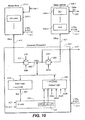
- Dispositif de stockage (600) comprenant une mémoire EEPROM à mémoire flash, la mémoire EEPROM comprenant :une matrice de mémoire flash (602) comprenant une zone masquée (604) et une zone de données d'utilisateur (606) ; etun montage de circuits périphériques comprenant un registre à bits multiples (610) ;caractérisé en ce queun code à bits multiples aléatoires ou pseudo-aléatoires est stocké dans le registre ;le dispositif de stockage (600) comprend en outre un comparateur destiné à comparer chaque bit du code à une adresse de page d'une page de données, en vue d'inverser le schéma de codage de la page ou de laisser le schéma de codage tel quel.
- Dispositif de stockage selon la revendication 1, dans lequel un circuit (310) est apte à stocker tout d'abord le code dans la zone masquée de la matrice, et à le transférer ensuite au registre.
- Dispositif de stockage selon la revendication 2, dans lequel le circuit (310) est apte à transférer le code au registre, suite à la mise sous tension de la mémoire EEPROM.
- Dispositif de stockage selon la revendication 1, dans lequel la mémoire EEPROM comprend en outre un multiplexeur (614), et dans lequel le comparateur génère un bit de polarité pour une ou plusieurs pages par l'intermédiaire du multiplexeur.
- Dispositif de stockage selon la revendication 1, comprenant en outre :des circuits de génération de signaux d'horloge (310) destinés à générer un signal d'horloge de machine à états finis et un signal d'horloge de commande ;un circuit de référencement d'horloge destiné à générer un bit de polarité en référençant le signal d'horloge de machine à états finis et le signal d'horloge de commande ; etdes circuits aptes à appliquer un premier type de codage pour une première valeur du bit de polarité, et un second type de codage pour une seconde valeur du bit de polarité.
- Dispositif de stockage selon la revendication 5, dans lequel le circuit de référencement d'horloge génère un bit de polarité en référençant le signal d'horloge de machine à états finis au niveau du front montant du signal d'horloge de commande.
- Procédé de stockage de données dans une mémoire non volatile (600) présentant une pluralité de pages de données, consistant à :stocker, dans la mémoire non volatile, un code comprenant une pluralité de bits aléatoires ou pseudo-aléatoires, chaque bit de la pluralité déterminant si le codage de données d'une page de la pluralité doit être inversé ou doit rester tel quel ;lire le code à partir de la mémoire non volatile ;transférer le code de la mémoire non volatile (604) à un registre (610) affecté en vue de stocker la pluralité de bits du code ;stocker le code dans le registre (610) ;générer un signal de polarité en comparant une adresse de page d'une page de la pluralité de pages à un bit du code pour chaque bit du code ; etchanger le codage d'un sous-ensemble de pages de la pluralité sur la base du signal de polarité généré.
- Procédé selon la revendication 7, consistant en outre à multiplexer le signal de polarité de sorte qu'il s'applique à un groupe de la pluralité de pages et que le codage du groupe est déterminé par un unique bit du code.
- Procédé selon la revendication 7, dans lequel le code comprend 17 bits ou plus.
- Procédé selon la revendication 7, dans lequel le stockage du code dans la mémoire non volatile consiste à stocker le code dans une partition masquée (604) de la mémoire non volatile.
- Procédé selon la revendication 7, dans lequel la lecture du code à partir de la mémoire non volatile est mise en oeuvre au cours de la mise sous tension de la mémoire.
- Procédé selon la revendication 7, consistant en outre à lire une ou plusieurs pages de données d'utilisateur, dans lequel la lecture consiste à déterminer la polarité de chaque page devant être lue, par le biais de l'adresse de page.
- Procédé de mise en oeuvre d'une randomisation des données stockées dans une mémoire non volatile (600) présentant une pluralité de pages de données, consistant à :recevoir une commande d'utilisateur visant à programmer ou à lire les données d'utilisateur dans la matrice ; etcaractérisé en ce qu'il consiste à :suite à la réception de la commande d'utilisateur, déclencher l'application d'un code comprenant une pluralité de bits à un bloc des données d'utilisateur en vue de randomiser le codage des données d'utilisateur, chacun des bits du code déterminant si un groupe d'une ou plusieurs pages du bloc est stocké tel quel ou est inversé avant d'être stocké.
- Procédé selon la revendication 13, consistant en outre à stocker le code avec les données d'utilisateur traitées par le code.
- Procédé selon la revendication 13, dans lequel le code comprend 17 bits ou plus.
- Procédé selon la revendication 13, dans lequel le code est mis à jour entre les commandes d'utilisateur.
- Procédé selon la revendication 13, dans lequel, si le code comporte moins de bits que le nombre de pages au sein d'un bloc, le code est appliqué à plus d'un groupe d'une ou plusieurs pages.
- Procédé selon la revendication 14, dans lequel le procédé consiste en outre à lire le code stocké pour chaque segment, et pour chaque segment, à retourner les données d'utilisateur sur une base « bit par bit » au schéma de codage présent avant l'application du code.
Applications Claiming Priority (4)
| Application Number | Priority Date | Filing Date | Title |
|---|---|---|---|
| US11/530,392 US7734861B2 (en) | 2006-09-08 | 2006-09-08 | Pseudo random and command driven bit compensation for the cycling effects in flash memory |
| US11/530,399 US7606966B2 (en) | 2006-09-08 | 2006-09-08 | Methods in a pseudo random and command driven bit compensation for the cycling effects in flash memory |
| PCT/US2007/077940 WO2008031074A1 (fr) | 2006-09-08 | 2007-09-07 | Compensation de bits pseudo-aléatoire et dirigée par la commande pour les effets de cycle en mémoire flash et ses procédés |
| US11/852,229 US7885112B2 (en) | 2007-09-07 | 2007-09-07 | Nonvolatile memory and method for on-chip pseudo-randomization of data within a page and between pages |
Publications (2)
| Publication Number | Publication Date |
|---|---|
| EP2070090A1 EP2070090A1 (fr) | 2009-06-17 |
| EP2070090B1 true EP2070090B1 (fr) | 2014-01-08 |
Family
ID=38941921
Family Applications (1)
| Application Number | Title | Priority Date | Filing Date |
|---|---|---|---|
| EP07842100.5A Active EP2070090B1 (fr) | 2006-09-08 | 2007-09-07 | Compensation de bits pseudo-aléatoire et dirigée par la commande pour les effets de cycle en mémoire flash et ses procédés |
Country Status (4)
| Country | Link |
|---|---|
| EP (1) | EP2070090B1 (fr) |
| JP (1) | JP4778585B2 (fr) |
| KR (1) | KR101615773B1 (fr) |
| WO (1) | WO2008031074A1 (fr) |
Families Citing this family (14)
| Publication number | Priority date | Publication date | Assignee | Title |
|---|---|---|---|---|
| US7885112B2 (en) * | 2007-09-07 | 2011-02-08 | Sandisk Corporation | Nonvolatile memory and method for on-chip pseudo-randomization of data within a page and between pages |
| US7734861B2 (en) | 2006-09-08 | 2010-06-08 | Sandisk Corporation | Pseudo random and command driven bit compensation for the cycling effects in flash memory |
| US7606966B2 (en) | 2006-09-08 | 2009-10-20 | Sandisk Corporation | Methods in a pseudo random and command driven bit compensation for the cycling effects in flash memory |
| CN102132350B (zh) * | 2008-07-01 | 2015-06-17 | Lsi公司 | 用于闪存存储器中的软解映射和单元间干扰减轻的方法和设备 |
| US8429330B2 (en) | 2008-09-12 | 2013-04-23 | Sandisk Technologies Inc. | Method for scrambling data in which scrambling data and scrambled data are stored in corresponding non-volatile memory locations |
| WO2010030701A1 (fr) * | 2008-09-12 | 2010-03-18 | Sandisk Corporation | Embrouilleur de données intégré sur puce pour mémoire non volatile |
| US8145855B2 (en) | 2008-09-12 | 2012-03-27 | Sandisk Technologies Inc. | Built in on-chip data scrambler for non-volatile memory |
| KR20100099961A (ko) * | 2009-03-04 | 2010-09-15 | 삼성전자주식회사 | 불휘발성 메모리 장치 및 그 동작 방법 |
| KR101504338B1 (ko) | 2009-03-04 | 2015-03-23 | 삼성전자주식회사 | 불휘발성 메모리 장치의 동작 방법 |
| US8843693B2 (en) | 2011-05-17 | 2014-09-23 | SanDisk Technologies, Inc. | Non-volatile memory and method with improved data scrambling |
| US9292428B2 (en) | 2012-09-05 | 2016-03-22 | Kabushiki Kaisha Toshiba | Memory system |
| KR20160127525A (ko) | 2015-04-27 | 2016-11-04 | 에스케이하이닉스 주식회사 | 메모리 시스템 및 메모리 시스템의 동작 방법 |
| FR3095547A1 (fr) | 2019-04-26 | 2020-10-30 | Stmicroelectronics (Rousset) Sas | Bus de données de mémoire non-volatile |
| KR20210115524A (ko) | 2020-03-13 | 2021-09-27 | 삼성전자주식회사 | 반도체 메모리 장치 및 이의 제조 방법 |
Family Cites Families (6)
| Publication number | Priority date | Publication date | Assignee | Title |
|---|---|---|---|---|
| JPH07240098A (ja) * | 1994-02-25 | 1995-09-12 | Sony Corp | 半導体不揮発性記憶装置 |
| KR0172366B1 (ko) * | 1995-11-10 | 1999-03-30 | 김광호 | 불휘발성 반도체 메모리 장치의 독출 및 프로그램 방법과 그 회로 |
| JP3881869B2 (ja) * | 2001-11-05 | 2007-02-14 | 株式会社ルネサステクノロジ | 半導体記憶装置 |
| US7274596B2 (en) * | 2004-06-30 | 2007-09-25 | Micron Technology, Inc. | Reduction of adjacent floating gate data pattern sensitivity |
| US7120051B2 (en) | 2004-12-14 | 2006-10-10 | Sandisk Corporation | Pipelined programming of non-volatile memories using early data |
| CN1838323A (zh) * | 2005-01-19 | 2006-09-27 | 赛芬半导体有限公司 | 可预防固定模式编程的方法 |
-
2007
- 2007-09-07 EP EP07842100.5A patent/EP2070090B1/fr active Active
- 2007-09-07 JP JP2009527598A patent/JP4778585B2/ja not_active Expired - Fee Related
- 2007-09-07 KR KR1020097005011A patent/KR101615773B1/ko not_active IP Right Cessation
- 2007-09-07 WO PCT/US2007/077940 patent/WO2008031074A1/fr active Application Filing
Also Published As
| Publication number | Publication date |
|---|---|
| JP2010503142A (ja) | 2010-01-28 |
| KR20090074733A (ko) | 2009-07-07 |
| WO2008031074A1 (fr) | 2008-03-13 |
| KR101615773B1 (ko) | 2016-04-26 |
| JP4778585B2 (ja) | 2011-09-21 |
| EP2070090A1 (fr) | 2009-06-17 |
Similar Documents
| Publication | Publication Date | Title |
|---|---|---|
| US7734861B2 (en) | Pseudo random and command driven bit compensation for the cycling effects in flash memory | |
| EP1864289B1 (fr) | Utilisation de verrous de donnees dans des operations de cache de memoire non volatile | |
| EP2186094B1 (fr) | Mémoire non volatile et procédé pour une distribution pseudo-aléatoire sur puce de données à l'intérieur d'une page et entre des pages | |
| EP2070090B1 (fr) | Compensation de bits pseudo-aléatoire et dirigée par la commande pour les effets de cycle en mémoire flash et ses procédés | |
| US7606966B2 (en) | Methods in a pseudo random and command driven bit compensation for the cycling effects in flash memory | |
| JP4814995B2 (ja) | 読み出し操作中にデータラッチでバックグラウンドキャッシングを行う不揮発性メモリとその方法 | |
| EP1869681B1 (fr) | Utilisation de verrouillages de donnees dans la programmation a phases multiples de memoires non volatiles | |
| US8873303B2 (en) | Non-volatile memory and method with shared processing for an aggregate of read/write circuits | |
| US7345928B2 (en) | Data recovery methods in multi-state memory after program fail | |
| WO2006107651A1 (fr) | Memoire a etats multiples possedant une recuperation de donnees apres un echec de programme |
Legal Events
| Date | Code | Title | Description |
|---|---|---|---|
| PUAI | Public reference made under article 153(3) epc to a published international application that has entered the european phase |
Free format text: ORIGINAL CODE: 0009012 |
|
| 17P | Request for examination filed |
Effective date: 20090216 |
|
| AK | Designated contracting states |
Kind code of ref document: A1 Designated state(s): AT BE BG CH CY CZ DE DK EE ES FI FR GB GR HU IE IS IT LI LT LU LV MC MT NL PL PT RO SE SI SK TR |
|
| AX | Request for extension of the european patent |
Extension state: AL BA HR MK RS |
|
| 17Q | First examination report despatched |
Effective date: 20100601 |
|
| RAP1 | Party data changed (applicant data changed or rights of an application transferred) |
Owner name: SANDISK TECHNOLOGIES INC. |
|
| DAX | Request for extension of the european patent (deleted) | ||
| REG | Reference to a national code |
Ref country code: DE Ref legal event code: R079 Ref document number: 602007034714 Country of ref document: DE Free format text: PREVIOUS MAIN CLASS: G11C0016340000 Ipc: G11C0007020000 |
|
| RIC1 | Information provided on ipc code assigned before grant |
Ipc: G11C 16/10 20060101ALI20130419BHEP Ipc: G11C 7/02 20060101AFI20130419BHEP Ipc: G11C 11/56 20060101ALI20130419BHEP Ipc: G11C 16/34 20060101ALI20130419BHEP Ipc: G11C 7/10 20060101ALI20130419BHEP Ipc: G11C 16/04 20060101ALI20130419BHEP Ipc: G11C 7/20 20060101ALI20130419BHEP |
|
| GRAP | Despatch of communication of intention to grant a patent |
Free format text: ORIGINAL CODE: EPIDOSNIGR1 |
|
| INTG | Intention to grant announced |
Effective date: 20130726 |
|
| GRAS | Grant fee paid |
Free format text: ORIGINAL CODE: EPIDOSNIGR3 |
|
| GRAA | (expected) grant |
Free format text: ORIGINAL CODE: 0009210 |
|
| AK | Designated contracting states |
Kind code of ref document: B1 Designated state(s): AT BE BG CH CY CZ DE DK EE ES FI FR GB GR HU IE IS IT LI LT LU LV MC MT NL PL PT RO SE SI SK TR |
|
| REG | Reference to a national code |
Ref country code: GB Ref legal event code: FG4D |
|
| REG | Reference to a national code |
Ref country code: CH Ref legal event code: EP |
|
| REG | Reference to a national code |
Ref country code: IE Ref legal event code: FG4D |
|
| REG | Reference to a national code |
Ref country code: AT Ref legal event code: REF Ref document number: 649156 Country of ref document: AT Kind code of ref document: T Effective date: 20140215 |
|
| REG | Reference to a national code |
Ref country code: DE Ref legal event code: R096 Ref document number: 602007034714 Country of ref document: DE Effective date: 20140220 |
|
| REG | Reference to a national code |
Ref country code: AT Ref legal event code: MK05 Ref document number: 649156 Country of ref document: AT Kind code of ref document: T Effective date: 20140108 |
|
| REG | Reference to a national code |
Ref country code: NL Ref legal event code: VDEP Effective date: 20140108 |
|
| REG | Reference to a national code |
Ref country code: LT Ref legal event code: MG4D |
|
| PG25 | Lapsed in a contracting state [announced via postgrant information from national office to epo] |
Ref country code: LT Free format text: LAPSE BECAUSE OF FAILURE TO SUBMIT A TRANSLATION OF THE DESCRIPTION OR TO PAY THE FEE WITHIN THE PRESCRIBED TIME-LIMIT Effective date: 20140108 Ref country code: IS Free format text: LAPSE BECAUSE OF FAILURE TO SUBMIT A TRANSLATION OF THE DESCRIPTION OR TO PAY THE FEE WITHIN THE PRESCRIBED TIME-LIMIT Effective date: 20140508 |
|
| PG25 | Lapsed in a contracting state [announced via postgrant information from national office to epo] |
Ref country code: ES Free format text: LAPSE BECAUSE OF FAILURE TO SUBMIT A TRANSLATION OF THE DESCRIPTION OR TO PAY THE FEE WITHIN THE PRESCRIBED TIME-LIMIT Effective date: 20140108 Ref country code: PT Free format text: LAPSE BECAUSE OF FAILURE TO SUBMIT A TRANSLATION OF THE DESCRIPTION OR TO PAY THE FEE WITHIN THE PRESCRIBED TIME-LIMIT Effective date: 20140508 Ref country code: AT Free format text: LAPSE BECAUSE OF FAILURE TO SUBMIT A TRANSLATION OF THE DESCRIPTION OR TO PAY THE FEE WITHIN THE PRESCRIBED TIME-LIMIT Effective date: 20140108 Ref country code: FI Free format text: LAPSE BECAUSE OF FAILURE TO SUBMIT A TRANSLATION OF THE DESCRIPTION OR TO PAY THE FEE WITHIN THE PRESCRIBED TIME-LIMIT Effective date: 20140108 Ref country code: SE Free format text: LAPSE BECAUSE OF FAILURE TO SUBMIT A TRANSLATION OF THE DESCRIPTION OR TO PAY THE FEE WITHIN THE PRESCRIBED TIME-LIMIT Effective date: 20140108 Ref country code: CY Free format text: LAPSE BECAUSE OF FAILURE TO SUBMIT A TRANSLATION OF THE DESCRIPTION OR TO PAY THE FEE WITHIN THE PRESCRIBED TIME-LIMIT Effective date: 20140108 Ref country code: NL Free format text: LAPSE BECAUSE OF FAILURE TO SUBMIT A TRANSLATION OF THE DESCRIPTION OR TO PAY THE FEE WITHIN THE PRESCRIBED TIME-LIMIT Effective date: 20140108 |
|
| PG25 | Lapsed in a contracting state [announced via postgrant information from national office to epo] |
Ref country code: BE Free format text: LAPSE BECAUSE OF FAILURE TO SUBMIT A TRANSLATION OF THE DESCRIPTION OR TO PAY THE FEE WITHIN THE PRESCRIBED TIME-LIMIT Effective date: 20140108 Ref country code: LV Free format text: LAPSE BECAUSE OF FAILURE TO SUBMIT A TRANSLATION OF THE DESCRIPTION OR TO PAY THE FEE WITHIN THE PRESCRIBED TIME-LIMIT Effective date: 20140108 |
|
| REG | Reference to a national code |
Ref country code: DE Ref legal event code: R097 Ref document number: 602007034714 Country of ref document: DE |
|
| PG25 | Lapsed in a contracting state [announced via postgrant information from national office to epo] |
Ref country code: RO Free format text: LAPSE BECAUSE OF FAILURE TO SUBMIT A TRANSLATION OF THE DESCRIPTION OR TO PAY THE FEE WITHIN THE PRESCRIBED TIME-LIMIT Effective date: 20140108 Ref country code: CZ Free format text: LAPSE BECAUSE OF FAILURE TO SUBMIT A TRANSLATION OF THE DESCRIPTION OR TO PAY THE FEE WITHIN THE PRESCRIBED TIME-LIMIT Effective date: 20140108 Ref country code: EE Free format text: LAPSE BECAUSE OF FAILURE TO SUBMIT A TRANSLATION OF THE DESCRIPTION OR TO PAY THE FEE WITHIN THE PRESCRIBED TIME-LIMIT Effective date: 20140108 Ref country code: DK Free format text: LAPSE BECAUSE OF FAILURE TO SUBMIT A TRANSLATION OF THE DESCRIPTION OR TO PAY THE FEE WITHIN THE PRESCRIBED TIME-LIMIT Effective date: 20140108 |
|
| PLBE | No opposition filed within time limit |
Free format text: ORIGINAL CODE: 0009261 |
|
| STAA | Information on the status of an ep patent application or granted ep patent |
Free format text: STATUS: NO OPPOSITION FILED WITHIN TIME LIMIT |
|
| PG25 | Lapsed in a contracting state [announced via postgrant information from national office to epo] |
Ref country code: PL Free format text: LAPSE BECAUSE OF FAILURE TO SUBMIT A TRANSLATION OF THE DESCRIPTION OR TO PAY THE FEE WITHIN THE PRESCRIBED TIME-LIMIT Effective date: 20140108 Ref country code: SK Free format text: LAPSE BECAUSE OF FAILURE TO SUBMIT A TRANSLATION OF THE DESCRIPTION OR TO PAY THE FEE WITHIN THE PRESCRIBED TIME-LIMIT Effective date: 20140108 |
|
| 26N | No opposition filed |
Effective date: 20141009 |
|
| REG | Reference to a national code |
Ref country code: DE Ref legal event code: R097 Ref document number: 602007034714 Country of ref document: DE Effective date: 20141009 |
|
| PG25 | Lapsed in a contracting state [announced via postgrant information from national office to epo] |
Ref country code: LU Free format text: LAPSE BECAUSE OF FAILURE TO SUBMIT A TRANSLATION OF THE DESCRIPTION OR TO PAY THE FEE WITHIN THE PRESCRIBED TIME-LIMIT Effective date: 20140907 Ref country code: MC Free format text: LAPSE BECAUSE OF FAILURE TO SUBMIT A TRANSLATION OF THE DESCRIPTION OR TO PAY THE FEE WITHIN THE PRESCRIBED TIME-LIMIT Effective date: 20140108 |
|
| REG | Reference to a national code |
Ref country code: CH Ref legal event code: PL |
|
| PG25 | Lapsed in a contracting state [announced via postgrant information from national office to epo] |
Ref country code: SI Free format text: LAPSE BECAUSE OF FAILURE TO SUBMIT A TRANSLATION OF THE DESCRIPTION OR TO PAY THE FEE WITHIN THE PRESCRIBED TIME-LIMIT Effective date: 20140108 |
|
| REG | Reference to a national code |
Ref country code: IE Ref legal event code: MM4A |
|
| REG | Reference to a national code |
Ref country code: FR Ref legal event code: ST Effective date: 20150529 |
|
| PG25 | Lapsed in a contracting state [announced via postgrant information from national office to epo] |
Ref country code: CH Free format text: LAPSE BECAUSE OF NON-PAYMENT OF DUE FEES Effective date: 20140930 Ref country code: LI Free format text: LAPSE BECAUSE OF NON-PAYMENT OF DUE FEES Effective date: 20140930 |
|
| PG25 | Lapsed in a contracting state [announced via postgrant information from national office to epo] |
Ref country code: IE Free format text: LAPSE BECAUSE OF NON-PAYMENT OF DUE FEES Effective date: 20140907 Ref country code: FR Free format text: LAPSE BECAUSE OF NON-PAYMENT OF DUE FEES Effective date: 20140930 |
|
| PG25 | Lapsed in a contracting state [announced via postgrant information from national office to epo] |
Ref country code: BG Free format text: LAPSE BECAUSE OF FAILURE TO SUBMIT A TRANSLATION OF THE DESCRIPTION OR TO PAY THE FEE WITHIN THE PRESCRIBED TIME-LIMIT Effective date: 20140108 |
|
| PG25 | Lapsed in a contracting state [announced via postgrant information from national office to epo] |
Ref country code: IT Free format text: LAPSE BECAUSE OF FAILURE TO SUBMIT A TRANSLATION OF THE DESCRIPTION OR TO PAY THE FEE WITHIN THE PRESCRIBED TIME-LIMIT Effective date: 20140108 Ref country code: MT Free format text: LAPSE BECAUSE OF FAILURE TO SUBMIT A TRANSLATION OF THE DESCRIPTION OR TO PAY THE FEE WITHIN THE PRESCRIBED TIME-LIMIT Effective date: 20140108 Ref country code: GR Free format text: LAPSE BECAUSE OF FAILURE TO SUBMIT A TRANSLATION OF THE DESCRIPTION OR TO PAY THE FEE WITHIN THE PRESCRIBED TIME-LIMIT Effective date: 20140409 |
|
| PG25 | Lapsed in a contracting state [announced via postgrant information from national office to epo] |
Ref country code: HU Free format text: LAPSE BECAUSE OF FAILURE TO SUBMIT A TRANSLATION OF THE DESCRIPTION OR TO PAY THE FEE WITHIN THE PRESCRIBED TIME-LIMIT; INVALID AB INITIO Effective date: 20070907 Ref country code: TR Free format text: LAPSE BECAUSE OF FAILURE TO SUBMIT A TRANSLATION OF THE DESCRIPTION OR TO PAY THE FEE WITHIN THE PRESCRIBED TIME-LIMIT Effective date: 20140108 |
|
| REG | Reference to a national code |
Ref country code: DE Ref legal event code: R082 Ref document number: 602007034714 Country of ref document: DE Representative=s name: MARKS & CLERK (LUXEMBOURG) LLP, LU Ref country code: DE Ref legal event code: R081 Ref document number: 602007034714 Country of ref document: DE Owner name: SANDISK TECHNOLOGIES LLC, PLANO, US Free format text: FORMER OWNER: SANDISK TECHNOLOGIES INC., PLANO, TEX., US |
|
| PGFP | Annual fee paid to national office [announced via postgrant information from national office to epo] |
Ref country code: GB Payment date: 20180905 Year of fee payment: 12 |
|
| GBPC | Gb: european patent ceased through non-payment of renewal fee |
Effective date: 20190907 |
|
| PG25 | Lapsed in a contracting state [announced via postgrant information from national office to epo] |
Ref country code: GB Free format text: LAPSE BECAUSE OF NON-PAYMENT OF DUE FEES Effective date: 20190907 |
|
| P01 | Opt-out of the competence of the unified patent court (upc) registered |
Effective date: 20230606 |
|
| PGFP | Annual fee paid to national office [announced via postgrant information from national office to epo] |
Ref country code: DE Payment date: 20230712 Year of fee payment: 17 |