EP2186094B1 - Mémoire non volatile et procédé pour une distribution pseudo-aléatoire sur puce de données à l'intérieur d'une page et entre des pages - Google Patents
Mémoire non volatile et procédé pour une distribution pseudo-aléatoire sur puce de données à l'intérieur d'une page et entre des pages Download PDFInfo
- Publication number
- EP2186094B1 EP2186094B1 EP08830722A EP08830722A EP2186094B1 EP 2186094 B1 EP2186094 B1 EP 2186094B1 EP 08830722 A EP08830722 A EP 08830722A EP 08830722 A EP08830722 A EP 08830722A EP 2186094 B1 EP2186094 B1 EP 2186094B1
- Authority
- EP
- European Patent Office
- Prior art keywords
- page
- data
- memory
- read
- write
- Prior art date
- Legal status (The legal status is an assumption and is not a legal conclusion. Google has not performed a legal analysis and makes no representation as to the accuracy of the status listed.)
- Not-in-force
Links
- 230000015654 memory Effects 0.000 title claims abstract description 241
- 238000000034 method Methods 0.000 title claims description 70
- 230000006870 function Effects 0.000 claims description 18
- 230000001960 triggered effect Effects 0.000 claims description 6
- 238000007667 floating Methods 0.000 abstract description 44
- 238000003860 storage Methods 0.000 abstract description 34
- 230000008878 coupling Effects 0.000 abstract description 16
- 238000010168 coupling process Methods 0.000 abstract description 16
- 238000005859 coupling reaction Methods 0.000 abstract description 16
- 230000007774 longterm Effects 0.000 abstract description 2
- 230000008569 process Effects 0.000 description 31
- 238000006243 chemical reaction Methods 0.000 description 15
- 238000012546 transfer Methods 0.000 description 11
- 230000000694 effects Effects 0.000 description 10
- 230000008859 change Effects 0.000 description 8
- 238000012795 verification Methods 0.000 description 7
- 239000000758 substrate Substances 0.000 description 6
- 238000004891 communication Methods 0.000 description 5
- 230000001419 dependent effect Effects 0.000 description 5
- 238000013461 design Methods 0.000 description 5
- 238000010586 diagram Methods 0.000 description 5
- 230000007246 mechanism Effects 0.000 description 5
- 230000001360 synchronised effect Effects 0.000 description 5
- 101001072191 Homo sapiens Protein disulfide-isomerase A2 Proteins 0.000 description 4
- 101001098828 Homo sapiens Protein disulfide-isomerase A5 Proteins 0.000 description 4
- 102100036351 Protein disulfide-isomerase A2 Human genes 0.000 description 4
- 230000004048 modification Effects 0.000 description 4
- 238000012986 modification Methods 0.000 description 4
- 230000001603 reducing effect Effects 0.000 description 4
- 230000000630 rising effect Effects 0.000 description 4
- 230000008901 benefit Effects 0.000 description 3
- 230000000295 complement effect Effects 0.000 description 3
- 238000013500 data storage Methods 0.000 description 3
- 238000009792 diffusion process Methods 0.000 description 3
- 238000002347 injection Methods 0.000 description 3
- 239000007924 injection Substances 0.000 description 3
- 238000001745 non-dispersive infrared spectroscopy Methods 0.000 description 3
- 230000002093 peripheral effect Effects 0.000 description 3
- 238000012545 processing Methods 0.000 description 3
- 238000000638 solvent extraction Methods 0.000 description 3
- 230000007704 transition Effects 0.000 description 3
- VYPSYNLAJGMNEJ-UHFFFAOYSA-N Silicium dioxide Chemical compound O=[Si]=O VYPSYNLAJGMNEJ-UHFFFAOYSA-N 0.000 description 2
- 230000006399 behavior Effects 0.000 description 2
- 238000009826 distribution Methods 0.000 description 2
- 230000005684 electric field Effects 0.000 description 2
- 230000005669 field effect Effects 0.000 description 2
- 239000002784 hot electron Substances 0.000 description 2
- 238000004519 manufacturing process Methods 0.000 description 2
- 239000000203 mixture Substances 0.000 description 2
- 238000005192 partition Methods 0.000 description 2
- 229910021420 polycrystalline silicon Inorganic materials 0.000 description 2
- 229920005591 polysilicon Polymers 0.000 description 2
- 230000005855 radiation Effects 0.000 description 2
- 239000004065 semiconductor Substances 0.000 description 2
- 230000005689 Fowler Nordheim tunneling Effects 0.000 description 1
- 230000003044 adaptive effect Effects 0.000 description 1
- 230000003190 augmentative effect Effects 0.000 description 1
- 239000000872 buffer Substances 0.000 description 1
- 230000001808 coupling effect Effects 0.000 description 1
- 230000001351 cycling effect Effects 0.000 description 1
- 230000003247 decreasing effect Effects 0.000 description 1
- 238000001514 detection method Methods 0.000 description 1
- 230000001627 detrimental effect Effects 0.000 description 1
- 238000007599 discharging Methods 0.000 description 1
- 230000009977 dual effect Effects 0.000 description 1
- 238000005516 engineering process Methods 0.000 description 1
- 230000005283 ground state Effects 0.000 description 1
- 230000005764 inhibitory process Effects 0.000 description 1
- 230000016507 interphase Effects 0.000 description 1
- 230000009191 jumping Effects 0.000 description 1
- 230000007257 malfunction Effects 0.000 description 1
- 239000002184 metal Substances 0.000 description 1
- 230000002085 persistent effect Effects 0.000 description 1
- 230000003094 perturbing effect Effects 0.000 description 1
- 239000013643 reference control Substances 0.000 description 1
- 230000003252 repetitive effect Effects 0.000 description 1
- 230000000717 retained effect Effects 0.000 description 1
- 235000012239 silicon dioxide Nutrition 0.000 description 1
- 239000000377 silicon dioxide Substances 0.000 description 1
- 239000007787 solid Substances 0.000 description 1
- 239000000243 solution Substances 0.000 description 1
- 238000012360 testing method Methods 0.000 description 1
- 230000005641 tunneling Effects 0.000 description 1
Images


Classifications
-
- G—PHYSICS
- G11—INFORMATION STORAGE
- G11C—STATIC STORES
- G11C11/00—Digital stores characterised by the use of particular electric or magnetic storage elements; Storage elements therefor
- G11C11/56—Digital stores characterised by the use of particular electric or magnetic storage elements; Storage elements therefor using storage elements with more than two stable states represented by steps, e.g. of voltage, current, phase, frequency
- G11C11/5621—Digital stores characterised by the use of particular electric or magnetic storage elements; Storage elements therefor using storage elements with more than two stable states represented by steps, e.g. of voltage, current, phase, frequency using charge storage in a floating gate
- G11C11/5628—Programming or writing circuits; Data input circuits
-
- G—PHYSICS
- G11—INFORMATION STORAGE
- G11C—STATIC STORES
- G11C16/00—Erasable programmable read-only memories
- G11C16/02—Erasable programmable read-only memories electrically programmable
- G11C16/06—Auxiliary circuits, e.g. for writing into memory
- G11C16/08—Address circuits; Decoders; Word-line control circuits
-
- G—PHYSICS
- G11—INFORMATION STORAGE
- G11C—STATIC STORES
- G11C16/00—Erasable programmable read-only memories
- G11C16/02—Erasable programmable read-only memories electrically programmable
- G11C16/06—Auxiliary circuits, e.g. for writing into memory
- G11C16/10—Programming or data input circuits
-
- G—PHYSICS
- G11—INFORMATION STORAGE
- G11C—STATIC STORES
- G11C16/00—Erasable programmable read-only memories
- G11C16/02—Erasable programmable read-only memories electrically programmable
- G11C16/06—Auxiliary circuits, e.g. for writing into memory
- G11C16/34—Determination of programming status, e.g. threshold voltage, overprogramming or underprogramming, retention
- G11C16/3418—Disturbance prevention or evaluation; Refreshing of disturbed memory data
- G11C16/3427—Circuits or methods to prevent or reduce disturbance of the state of a memory cell when neighbouring cells are read or written
-
- G—PHYSICS
- G11—INFORMATION STORAGE
- G11C—STATIC STORES
- G11C7/00—Arrangements for writing information into, or reading information out from, a digital store
- G11C7/10—Input/output [I/O] data interface arrangements, e.g. I/O data control circuits, I/O data buffers
- G11C7/1006—Data managing, e.g. manipulating data before writing or reading out, data bus switches or control circuits therefor
-
- G—PHYSICS
- G11—INFORMATION STORAGE
- G11C—STATIC STORES
- G11C2211/00—Indexing scheme relating to digital stores characterized by the use of particular electric or magnetic storage elements; Storage elements therefor
- G11C2211/56—Indexing scheme relating to G11C11/56 and sub-groups for features not covered by these groups
- G11C2211/564—Miscellaneous aspects
- G11C2211/5647—Multilevel memory with bit inversion arrangement
Definitions
- the present invention relates generally to nonvolatile memory such as flash memory with charge storage elements, and more specifically to have the memory store data pseudo-randomly to avoid possible undesirable data patterns which could cause the memory to malfunction.
- a charge stored in one cell or portion of the array may influence a read or program operation of a neighboring cell. This is what as known as a read or program disturb and cell coupling.
- Flash memory is often used by some users to constantly store the same data pattern again and again repeatedly in some blocks of the flash memory. The result is that there will be some bits left to be erased but never programmed. Additionally, there will be also some bits always programmed and rarely erased. These persistent data patterns are problematic in that they may result in disturbs and other difficulties such as floating gate to floating gate effects, NAND string resistance effect, and reduced memory endurance and reliability, etc.
- Solid-state memory capable of nonvolatile storage of charge, particularly in the form of EEPROM and flash EEPROM packaged as a small form factor card, has recently become the storage of choice in a variety of mobile and handheld devices, notably information appliances and consumer electronics products.
- RAM random access memory
- flash memory is non-volatile, retaining its stored data even after power is turned off.
- flash memory is increasingly being used in mass storage applications.
- Conventional mass storage, based on rotating magnetic medium such as hard drives and floppy disks, is unsuitable for the mobile and handheld environment. This is because disk drives tend to be bulky, are prone to mechanical failure and have high latency and high power requirements.
- flash memory both embedded and in the form of a removable card is ideally suited in the mobile and handheld environment because of its small size, low power consumption, high speed and high reliability features.
- EEPROM and electrically programmable read-only memory are non-volatile memory that can be erased and have new data written or "programmed" into their memory cells. Both utilize a floating (unconnected) conductive gate, in a field effect transistor structure, positioned over a channel region in a semiconductor substrate, between source and drain regions. A control gate is then provided over the floating gate. The threshold voltage characteristic of the transistor is controlled by the amount of charge that is retained on the floating gate. That is, for a given level of charge on the floating gate, there is a corresponding voltage (threshold) that must be applied to the control gate before the transistor is turned “on” to permit conduction between its source and drain regions.
- threshold voltage characteristic of the transistor is controlled by the amount of charge that is retained on the floating gate. That is, for a given level of charge on the floating gate, there is a corresponding voltage (threshold) that must be applied to the control gate before the transistor is turned “on” to permit conduction between its source and drain regions.
- the floating gate can hold a range of charges and therefore can be programmed to any threshold voltage level within a threshold voltage window.
- the size of the threshold voltage window is delimited by the minimum and maximum threshold levels of the device, which in turn correspond to the range of the charges that can be programmed onto the floating gate.
- the threshold window generally depends on the memory device's characteristics, operating conditions and history. Each distinct, resolvable threshold voltage level range within the window may, in principle, be used to designate a definite memory state of the cell.
- the transistor serving as a memory cell is typically programmed to a "programmed" state by one of two mechanisms.
- hot electron injection a high voltage applied to the drain accelerates electrons across the substrate channel region.
- control gate pulls the hot electrons through a thin gate dielectric onto the floating gate.
- tunnel injection a high voltage is applied to the control gate relative to the substrate. In this way, electrons are pulled from the substrate to the intervening floating gate.
- the memory device may be erased by a number of mechanisms.
- EPROM the memory is bulk erasable by removing the charge from the floating gate by ultraviolet radiation.
- EEPROM a memory cell is electrically erasable, by applying a high voltage to the substrate relative to the control gate so as to induce electrons in the floating gate to tunnel through a thin oxide to the substrate channel region (i.e., Fowler-Nordheim tunneling.)
- the EEPROM is erasable byte by byte.
- flash EEPROM the memory is electrically erasable either all at once or one or more blocks at a time, where a block may consist of 512 bytes or more of memory.
- the memory devices typically comprise one or more memory chips that may be mounted on a card.
- Each memory chip comprises an array of memory cells supported by peripheral circuits such as decoders and erase, write and read circuits.
- peripheral circuits such as decoders and erase, write and read circuits.
- the more sophisticated memory devices also come with a controller that performs intelligent and higher level memory operations and interfacing.
- non-volatile solid-state memory devices may employ different types of memory cells, each type having one or more charge storage element.
- FIGs. 1A-1E illustrate schematically different examples of non-volatile memory cells.
- FIG. 1A illustrates schematically a non-volatile memory in the form of an EEPROM cell with a floating gate for storing charge.
- An electrically erasable and programmable read-only memory (EEPROM) has a similar structure to EPROM, but additionally provides a mechanism for loading and removing charge electrically from its floating gate upon application of proper voltages without the need for exposure to UV radiation. Examples of such cells and methods of manufacturing them are given in United States patent no. 5,595,924 .
- FIG. 1B illustrates schematically a flash EEPROM cell having both a select gate and a control or steering gate.
- the memory cell 10 has a "split-channel" 12 between source 14 and drain 16 diffusions.
- a cell is formed effectively with two transistors T1 and T2 in series.
- T1 serves as a memory transistor having a floating gate 20 and a control gate 30.
- the floating gate is capable of storing a selectable amount of charge. The amount of current that can flow through the T1's portion of the channel depends on the voltage on the control gate 30 and the amount of charge residing on the intervening floating gate 20.
- T2 serves as a select transistor having a select gate 40.
- T2 When T2 is turned on by a voltage at the select gate 40, it allows the current in the T1's portion of the channel to pass between the source and drain.
- the select transistor provides a switch along the source-drain channel independent of the voltage at the control gate.
- One advantage is that it can be used to turn off those cells that are still conducting at zero control gate voltage due to their charge depletion (positive) at their floating gates.
- the other advantage is that it allows source side injection programming to be more easily implemented.
- One simple embodiment of the split-channel memory cell is where the select gate and the control gate are connected to the same word line as indicated schematically by a dotted line shown in FIG. 1 B. This is accomplished by having a charge storage element (floating gate) positioned over one portion of the channel and a control gate structure (which is part of a word line) positioned over the other channel portion as well as over the charge storage element.
- a more refined embodiment of the split-channel cell shown in FIG. 1B is when the select gate and the control gate are independent and not connected by the dotted line between them.
- One implementation has the control gates of one column in an array of cells connected to a control (or steering) line perpendicular to the word line. The effect is to relieve the word line from having to perform two functions at the same time when reading or programming a selected cell. Those two functions are (1) to serve as a gate of a select transistor, thus requiring a proper voltage to turn the select transistor on and off, and (2) to drive the voltage of the charge storage element to a desired level through an electric field (capacitive) coupling between the word line and the charge storage element. It is often difficult to perform both of these functions in an optimum manner with a single voltage.
- FIG. 1C illustrates schematically another flash EEPROM cell having dual floating gates and independent select and control gates.
- the memory cell 10 is similar to that of FIG. 1B except it effectively has three transistors in series.
- two storage elements i.e., that of T1 - left and T1 - right
- the memory transistors have floating gates 20 and 20', and control gates 30 and 30', respectively.
- the select transistor T2 is controlled by a select gate 40. At any one time, only one of the pair of memory transistors is accessed for read or write.
- both the T2 and T1 - right are turned on to allow the current in the T1 - left's portion of the channel to pass between the source and the drain.
- T2 and T1 - left are turned on.
- Erase is effected by having a portion of the select gate polysilicon in close proximity to the floating gate and applying a substantial positive voltage (e.g. 20V) to the select gate so that the electrons stored within the floating gate can tunnel to the select gate polysilicon.
- FIG. 1D illustrates schematically a string of memory cells organized into an NAND cell.
- a pair of select transistors S1, S2 controls the memory transistors chain's connection to the external via the NAND cell's source terminal 54 and drain terminal 56.
- the source select transistor S1 when the source select transistor S1 is turned on, the source terminal is coupled to a source line.
- the drain select transistor S2 is turned on, the drain terminal of the NAND cell is coupled to a bit line of the memory array.
- Each memory transistor in the chain has a charge storage element to store a given amount of charge so as to represent an intended memory state.
- a control gate of each memory transistor provides control over read and write operations.
- a control gate of each of the select transistors S1, S2 provides control access to the NAND cell via its source terminal 54 and drain terminal 56 respectively.
- FIG. 1E illustrates schematically a non-volatile memory with a dielectric layer for storing charge.
- a dielectric layer is used.
- Such memory devices utilizing dielectric storage element have been described by Eitan et al., "NROM: A Novel Localized Trapping, 2-Bit Nonvolatile Memory Cell,” IEEE Electron Device Letters, vol. 21, no. 11, November 2000, pp. 543-545 .
- An ONO dielectric layer extends across the channel between source and drain diffusions. The charge for one data bit is localized in the dielectric layer adjacent to the drain, and the charge for the other data bit is localized in the dielectric layer adjacent to the source.
- United States patents nos. 5,768,192 and 6,011,725 disclose a nonvolatile memory cell having a trapping dielectric sandwiched between two silicon dioxide layers. Multi-state data storage is implemented by separately reading the binary states of the spatially separated charge storage regions within the dielectric.
- a memory device typically comprises of a two-dimensional array of memory cells arranged in rows and columns and addressable by word lines and bit lines.
- the array can be formed according to an NOR type or an NAND type architecture.
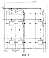
- FIG. 2 illustrates an example of an NOR array of memory cells.
- Memory devices with an NOR type architecture have been implemented with cells of the type illustrated in FIGs. 1B or 1C .
- Each row of memory cells are connected by their sources and drains in a daisy-chain manner. This design is sometimes referred to as a virtual ground design.
- Each memory cell 10 has a source 14, a drain 16, a control gate 30 and a select gate 40.
- the cells in a row have their select gates connected to word line 42.
- the cells in a column have their sources and drains respectively connected to selected bit lines 34 and 36.
- a steering line 36 also connects the control gates of the cells in a column.
- flash EEPROM devices are implemented with memory cells where each is formed with its control gate and select gate connected together. In this case, there is no need for steering lines and a word line simply connects all the control gates and select gates of cells along each row. Examples of these designs are disclosed in United States patent nos. 5,172,338 and 5,418,752 . In these designs, the word line essentially performed two functions: row selection and supplying control gate voltage to all cells in the row for reading or programming.
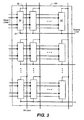
- FIG. 3 illustrates an example of an NAND array of memory cells, such as that shown in FIG. 1D .
- a bit line is coupled to the drain terminal 56 of each NAND cell.
- a source line may connect all their source terminals 54.
- the control gates of the NAND cells along a row are connected to a series of corresponding word lines. An entire row of NAND cells can be addressed by turning on the pair of select transistors (see FIG. 1D ) with appropriate voltages on their control gates via the connected word lines.
- Erase circuits are provided to erase one or more blocks of memory cells.
- a non-volatile memory such as EEPROM is referred to as a "Flash" EEPROM when an entire array of cells, or significant groups of cells of the array, is electrically erased together (i.e., in a flash). Once erased, the group of cells can then be reprogrammed.
- the group of cells erasable together may consist one or more addressable erase unit.
- the erase unit or block typically stores one or more pages of data, the page being the unit of programming and reading, although more than one page may be programmed or read in a single operation.
- Each page typically stores one or more sectors of data, the size of the sector being defined by the host system.
- An example is a sector of 512 bytes of user data, following a standard established with magnetic disk drives, plus some number of bytes of overhead information about the user data and/or the block in with it is stored.
- At least one current breakpoint level is established so as to partition the conduction window into two regions.
- a cell When a cell is read by applying predetermined, fixed voltages, its source/drain current is resolved into a memory state by comparing with the breakpoint level (or reference current I REF ). If the current read is higher than that of the breakpoint level, the cell is determined to be in one logical state (e.g., a "zero" state). On the other hand, if the current is less than that of the breakpoint level, the cell is determined to be in the other logical state (e.g., a "one" state). Thus, such a two-state cell stores one bit of digital information.
- a reference current source which may be externally programmable, is often provided as part of a memory system to generate the breakpoint level current.
- flash EEPROM devices are being fabricated with higher and higher density as the state of the semiconductor technology advances.
- Another method for increasing storage capacity is to have each memory cell store more than two states.
- the conduction window is partitioned into more than two regions by more than one breakpoint such that each cell is capable of storing more than one bit of data.
- the information that a given EEPROM array can store is thus increased with the number of states that each cell can store.
- EEPROM or flash EEPROM with multi-state or multi-level memory cells have been described in U.S. Patent No. 5,172,338 .
- the memory state of a cell is usually read by sensing the conduction current across the source and drain electrodes of the cell when a reference voltage is applied to the control gate.
- a corresponding conduction current with respect to a fixed reference control gate voltage may be detected.
- the range of charge programmable onto the floating gate defines a corresponding threshold voltage window or a corresponding conduction current window.
- the threshold voltage for a given memory state under test is set at the control gate and detect if the conduction current is lower or higher than a threshold current.
- the detection of the conduction current relative to a threshold current is accomplished by examining the rate the conduction current is discharging through the capacitance of the bit line.
- FIG. 4 illustrates the relation between the source-drain current I D and the control gate voltage V CG for four different charges Q1-Q4 that the floating gate may be selectively storing at any one time.
- the four solid I D versus V CG curves represent four possible charge levels that can be programmed on a floating gate of a memory cell, respectively corresponding to four possible memory states.
- the threshold voltage window of a population of cells may range from 0.5V to 3.5V.
- Six memory states may be demarcated by partitioning the threshold window into five regions in interval of 0.5V each.
- Q4 is in a memory state "5".
- United States Patent No. 4,357,685 discloses a method of programming a 2-state EPROM in which when a cell is programmed to a given state, it is subject to successive programming voltage pulses, each time adding incremental charge to the floating gate. In between pulses, the cell is read back or verified to determine its source-drain current relative to the breakpoint level. Programming stops when the current state has been verified to reach the desired state.
- the programming pulse train used may have increasing period or amplitude.
- Prior art programming circuits simply apply programming pulses to step through the threshold window from the erased or ground state until the target state is reached. Practically, to allow for adequate resolution, each partitioned or demarcated region would require at least about five programming steps to transverse. The performance is acceptable for 2-state memory cells. However, for multi-state cells, the number of steps required increases with the number of partitions and therefore, the programming precision or resolution must be increased. For example, a 16-state cell may require on average at least 40 programming pulses to program to a target state.
- FIG. 5 illustrates schematically a memory device with a typical arrangement of a memory array 100 accessible by read/write circuits 170 via row decoder 130 and column decoder 160.
- a memory transistor of a memory cell in the memory array 100 is addressable via a set of selected word line(s) and bit line(s).
- the row decoder 130 selects one or more word lines and the column decoder 160 selects one or more bit lines in order to apply appropriate voltages to the respective gates of the addressed memory transistor.
- Read/write circuits 170 are provided to read or write (program) the memory states of addressed memory transistors.
- the read/write circuits 170 comprise a number of read/write modules connectable via bit lines to memory elements in the array.
- FIG. 6A is a schematic block diagram of an individual read/write module 190.
- a sense amplifier determines the current flowing through the drain of an addressed memory transistor connected via a selected bit line. The current depends on the charge stored in the memory transistor and its control gate voltage. For example, in a multi-state EEPROM cell, its floating gate can be charged to one of several different levels. For a 4-level cell, it may be used to store two bits of data. The level detected by the sense amplifier is converted by a level-to-bits conversion logic to a set of data bits to be stored in a data latch.
- a logical "page" of memory elements are read or programmed together.
- a row typically contains several interleaved pages. All memory elements of a page will be read or programmed together.
- the column decoder will selectively connect each one of the interleaved pages to a corresponding number of read/write modules.
- the memory array is designed to have a page size of 532 bytes (512 bytes plus 20 bytes of overheads.) If each column contains a drain bit line and there are two interleaved pages per row, this amounts to 8512 columns with each page being associated with 4256 columns.
- the read/write modules forming the read/write circuits 170 can be arranged into various architectures.
- the read/write circuits 170 is organized into banks of read/write stacks 180.
- Each read/write stack 180 is a stack of read/write modules 190.
- the column spacing is determined by the size of the one or two transistors that occupy it.
- the circuitry of a read/write module will likely be implemented with many more transistors and circuit elements and therefore will occupy a space over many columns. In order to service more than one column among the occupied columns, multiple modules are stacked up on top of each other.
- FIG. 6B shows the read/write stack of FIG. 5 implemented conventionally by a stack of read/write modules 190.
- a read/write module may extend over sixteen columns, then a read/write stack 180 with a stack of eight read/write modules can be used to service eight columns in parallel.
- the read/write stack can be coupled via a column decoder to either the eight odd (1, 3, 5, 7, 9, 11, 13, 15) columns or the eight even (2, 4, 6, 8, 10, 12, 14, 16) columns among the bank.
- a block decoder is used to multiplex the set of read/write modules to either the even page or the odd page. In this way, whenever one set bit lines are being read or programmed, the interleaving set can be grounded to minimize immediate neighbor coupling.
- the interleaving page architecture is disadvantageous in at least three respects. First, it requires additional multiplexing circuitry. Secondly, it is slow in performance. To finish read or program of memory cells connected by a word line or in a row, two read or two program operations are required. Thirdly, it is also not optimum in addressing other disturb effects such as field coupling between neighboring charge storage elements at the floating gate level when the two neighbors are programmed at different times, such as separately in odd and even pages.
- the problem of neighboring field coupling becomes more pronounced with ever closer spacing between memory transistors.
- a charge storage element is sandwiched between a channel region and a control gate.
- the current that flows in the channel region is a function of the resultant electric field contributed by the field at the control gate and the charge storage element.
- memory transistors With ever increasing density, memory transistors are formed closer and closer together.
- the field from neighboring charge elements then becomes significant contributor to the resultant field of an affected cell.
- the neighboring field depends on the charge programmed into the charge storage elements of the neighbors. This perturbing field is dynamic in nature as it changes with the programmed states of the neighbors. Thus, an affected cell may read differently at different time depending on the changing states of the neighbors.
- the conventional architecture of interleaving page exacerbates the error caused by neighboring floating gate coupling. Since the even page and the odd page are programmed and read independently of each other, a page may be programmed under one set of condition but read back under an entirely different set of condition, depending on what has happened to the intervening page in the meantime.
- the read errors will become more severe with increasing density, requiring a more accurate read operation and coarser partitioning of the threshold window for multi-state implementation. Performance will suffer and the potential capacity in a multi-state implementation is limited.
- United States Patent Publication No. US-2004-0060031-A1 discloses a high performance yet compact non-volatile memory device having a large block of read/write circuits to read and write a corresponding block of memory cells in parallel.
- the memory device has an architecture that reduces redundancy in the block of read/write circuits to a minimum.
- Significant saving in space as well as power is accomplished by redistributing the block of read/write modules into a block read/write module core portions that operate in parallel while interacting with a substantially smaller sets of common portions in a time-multiplexing manner.
- data processing among read/write circuits between a plurality of sense amplifiers and data latches is performed by a shared processor.
- the present invention is directed at an integrated-circuit memory chip comprising an array of nonvolatile memory cells accessible page by page, each page being a group of memory cells, each memory cell of the group being in a column of the array and along a row accessible by a common word line.
- a sequence of starting column positions ( FIG. 27 ) is provided so that each page to be programmed has an associated starting column position; an address generator ( FIG. 27 ) generates an address for the associated starting column position, and a set of data latches is associated with each column responsive to the address generator for staging data to be programmed into each page, the staged data starting from the associated starting column position and wrapping around until the page is filled.
- a programming circuit is adapted to program in parallel the staged data into each page.
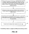
- the data in each memory page can be randomized such that when data from several pages are lined up problematic data patterns are avoided during programming.
- a simple way of scrambling the data on a page is to write the data on an independent or different starting address for each different page.
- a corresponding page of data is written to each page of memory cells at a different starting location for each page.
- the data is filled to the end of the page, it continues by wrapping around from the first address of the page until just before the starting location.
- a sequence of starting physical column addresses, one for each page, is provided by a pseudo-random generator.
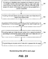
- the data bits in the page are randomized such that on average the page contains an equal mix of cells with erased and programmed states.
- the source line bias or loading does not vary substantially and can be allowed for with appropriate adjustment during the sensing operation.
- a sequence of pseudo random bits, each specifying a certain polarity is employed to encode bits within the page.
- the invention is also directed at a method for programming data into an array of nonvolatile memory cells in an integrated-circuit memory chip.
- the array is accessible page by page, each page being a group of memory cells, each memory cell of the group being in a column of the array and along a row accessible by a common word line.
- the method comprises:
- randomization within a page is combined with randomization from page to page.
- randomization within a page is preferably accomplished by each page having an independent starting position and randomization from page to page is preferably accomplished by each page having an independent encoding polarity.
- the randomization within a page implemented by each page having an independent starting position is also augmented by each set of data bits within a page having an independent encoding polarity.
- EEPROM memory chip
- the present invention will reduce or eliminate the specific data patterns which can cause program disturbs or user read disturbs, as well as reducing NAND string resistance effect, and increasing memory endurance and reliability. It will also reduce the problem of floating gate to floating gate coupling.
- FIGS. 1A-1E illustrate schematically different examples of non-volatile memory cells.
- FIG. 2 illustrates an example of an NOR array of memory cells.
- FIG. 3 illustrates an example of an NAND array of memory cells, such as that shown in FIG. 1D .
- FIG. 4 illustrates the relation between the source-drain current and the control gate voltage for four different charges Q1-Q4 that the floating gate may be storing at any one time.
- FIG. 5 illustrates schematically a typical arrangement of a memory array accessible by read/write circuits via row and column decoders.
- FIG. 6A is a schematic block diagram of an individual read/write module.
- FIG. 6B shows the read/write stack of FIG. 5 implemented conventionally by a stack of read/write modules.
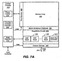
- FIG. 7A illustrates schematically a compact memory device having a bank of partitioned read/write stacks, in which the improved processor of the present invention is implemented.
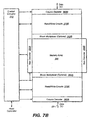
- FIG. 7B illustrates a preferred arrangement of the compact memory device shown in FIG. 7A .
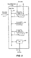
- FIG. 8 illustrates schematically a general arrangement of the basic components in a read/write stack shown in FIG. 7A .
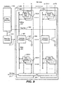
- FIG. 9 illustrates one preferred arrangement of the read/write stacks among the read/write circuits shown in FIGs. 7A and 7B .
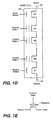
- FIG. 10 illustrates an improved embodiment of the common processor shown in FIG 9 .
- FIG. 11A illustrates a preferred embodiment of the input logic of the common processor shown in FIG. 10 .
- FIG. 11B illustrates the truth table of the input logic of FIG. 11A .
- FIG. 12A illustrates a preferred embodiment of the output logic of the common processor shown in FIG. 10 .
- FIG. 12B illustrates the truth table of the output logic of FIG. 12A .
- FIG. 13 is a simplified version of FIG. 10 that shows some specific elements that are relevant to the present discussion in a two-bit embodiment of the present invention
- FIG. 14 indicates the latch assignment for the same elements as FIG. 13 for upper page program where the lower page data is read in.
- FIG. 15 illustrates aspects of cache program in the single page mode.
- FIG. 16 shows a programming waveform that can be used in a lower page to full sequence conversion.
- FIG. 17 illustrates the relative timing in a cache program operation with a full sequence conversion.
- FIG. 18 describes the disposition of latches in a cache page copy operation.
- FIGS. 19A and 19B illustrate the relative timings in cache page copy operations.
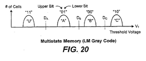
- FIG. 20 illustrates threshold voltage distributions of the 4-state memory array when each memory cell stores two bits of data using the LM code.
- FIG. 21 is a schematic block diagram of certain components of EEPROM or memory chip 600.
- FIG. 22A is an illustration of the encoding scheme and polarity bit of various pages of data by page address.
- FIG. 22B is a table illustrating the application of an example 17 bit code used to transform the encoding of user data.
- FIG. 22C illustrates application of polarity bits to the upper and lower bits stored in the memory cells of an exemplary NAND chain/string.
- FIG. 23A is an illustration of encoding scheme determination as a function of a command clock signal.
- FIG. 23B is a clock signal of a command.
- FIG. 23C illustrates an embodiment of control circuitry for data encoding determination and inversion.
- FIG. 23D illustrates a page of user data with the polarity bit stored therein.
- FIG. 23E illustrates an embodiment of control circuitry for reverting the encoding of potentially inverted data for read operations.
- FIG. 24A is a timeline of a command clock signal and a finite state machine clock signal showing the value of the FSM clock at the rising edge of the command clock signal.
- FIG. 24B illustrates exemplary circuitry to determine the polarity bit as a function of the command clock signal shown in FIG. 24A .
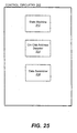
- FIG. 25 illustrates the On-chip control circuitry shown in FIG. 7A and FIG. 9 in more detail.
- FIG. 26 illustrates a method of scrambling the data on a memory page, according to one preferred embodiment of writing from different starting location for each page.
- FIG. 27 is a table illustrating an example of different pages having different starting locations for writing data.
- FIG. 28A illustrates the problem of source voltage error due to current flow in the source line having a finite resistance to ground.
- FIG. 28B illustrates the error in the threshold voltage level of a memory cell caused by a source line voltage drop.
- FIG. 29 illustrates a method of randomizing bits within a page.
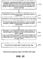
- FIG. 30 illustrates a method of randomizing data page-by-page and within each page, according to another aspect of the invention.
- FIG. 7A to FIG. 20 illustrate preferred memory systems in which the present invention is implemented.
- FIG. 7A illustrates schematically a compact memory device having a bank of partitioned read/write stacks, in which the improved processor of the present invention is implemented.
- the memory device includes a two-dimensional array of memory cells 300, control circuitry 310, and read/write circuits 370.
- the memory array 300 is addressable by word lines via a row decoder 330 and by bit lines via a column decoder 360.
- the read/write circuits 370 is implemented as a bank of partitioned read/write stacks 400 and allows a block (also referred to as a "page") of memory cells to be read or programmed in parallel.
- a page is constituted from a contiguous row of memory cells.
- a block multiplexer 350 is provided to multiplex the read/write circuits 370 to the individual blocks.
- the control circuitry 310 cooperates with the read/write circuits 370 to perform memory operations on the memory array 300.
- the control circuitry 310 includes a state machine 312, an on-chip address decoder 314 and a power control module 316.
- the state machine 312 provides chip level control of memory operations.
- the on-chip address decoder 314 provides an address interface between that used by the host or a memory controller to the hardware address used by the decoders 330 and 370.
- the power control module 316 controls the power and voltages supplied to the word lines and bit lines during memory operations.
- FIG. 7B illustrates a preferred arrangement of the compact memory device shown in FIG. 7A .
- Access to the memory array 300 by the various peripheral circuits is implemented in a symmetric fashion, on opposite sides of the array so that access lines and circuitry on each side are reduced in half.
- the row decoder is split into row decoders 330A and 330B and the column decoder into column decoders 360A and 360B.
- the block multiplexer 350 is split into block multiplexers 350A and 350B.
- the read/write circuits are split into read/write circuits 370A connecting to bit lines from the bottom and read/write circuits 370B connecting to bit lines from the top of the array300. In this way, the density of the read/write modules, and therefore that of the partitioned read/write stacks 400, is essentially reduced by one half.
- FIG. 8 illustrates schematically a general arrangement of the basic components in a read/write stack shown in FIG. 7A .
- the read/write stack 400 comprises a stack of sense amplifiers 212 for sensing k bit lines, an I/O module 440 for input or output of data via an I/O bus 231, a stack of data latches 430 for storing input or output data, a common processor 500 to process and store data among the read/write stack 400, and a stack bus 421 for communication among the stack components.
- a stack bus controller among the read/write circuits 370 provides control and timing signals via lines 411 for controlling the various components among the read/write stacks.
- FIG. 9 illustrates one preferred arrangement of the read/write stacks among the read/write circuits shown in FIGs. 7A and 7B .
- the entire bank of partitioned read/write stacks 400 operating in parallel allows a block (or page) ofp cells along a row to be read or programmed in parallel.
- p p/k.
- the block is a run of the entire row of cells.
- the block is a subset of cells in the row.
- the subset of cells could be one half of the entire row or one quarter of the entire row.
- the subset of cells could be a run of contiguous cells or one every other cell, or one every predetermined number of cells.
- Each read/write stack such as 400-1, essentially contains a stack of sense amplifiers 212-1 to 212-k servicing a segment of k memory cells in parallel.
- a preferred sense amplifier is disclosed in United States Patent Publication No. 2004-0109357-A1 .
- the stack bus controller 410 provides control and timing signals to the read/write circuit 370 via lines 411.
- the stack bus controller is itself dependent on the memory controller 310 via lines 311. Communication among each read/write stack 400 is effected by an interconnecting stack bus 431 and controlled by the stack bus controller 410.
- Control lines 411 provide control and clock signals from the stack bus controller 410 to the components of the read/write stacks 400-1.
- the stack bus is partitioned into a SABus 422 for communication between the common processor 500 and the stack of sense amplifiers 212, and a DBus 423 for communication between the processor and the stack of data latches 430.
- the stack of data latches 430 comprises of data latches 430-1 to 430-k, one for each memory cell associated with the stack
- the I/O module 440 enables the data latches to exchange data with the external via an I/O bus 231.
- the common processor also includes an output 507 for output of a status signal indicating a status of the memory operation, such as an error condition.
- the status signal is used to drive the gate of an n-transistor 550 that is tied to a FLAG BUS 509 in a Wired-Or configuration.
- the FLAG BUS is preferably precharged by the controller 310 and will be pulled down when a status signal is asserted by any of the read/write stacks.
- FIG. 10 illustrates an improved embodiment of the common processor shown in FIG 9 .
- the common processor 500 comprises a processor bus, PBUS 505 for communication with external circuits, an input logic 510, a processor latch PLatch 520 and an output logic 530.
- the input logic 510 receives data from the PBUS and outputs to a BSI node as a transformed data in one of logical states "1", “0", or “Z” (float) depending on the control signals from the stack bus controller 410 via signal lines 411.
- a Set/Reset latch, PLatch 520 then latches BSI, resulting in a pair of complementary output signals as MTCH and MTCH*.
- the output logic 530 receives the MTCH and MTCH* signals and outputs on the PBUS 505 a transformed data in one of logical states "1", “0", or "Z" (float) depending on the control signals from the stack bus controller 410 via signal lines 411.
- FIG. 10 illustrates the case for the memory cell coupled to bit line 1.
- the corresponding sense amplifier 212-1 comprises a node where the sense amplifier data appears.
- the node assumes the form of a SA Latch, 214-1 that stores data.
- the corresponding set of data latches 430-1 stores input or output data associated with the memory cell coupled to bit line 1.
- the set of data latches 430-1 comprises sufficient data latches, 434-1, ..., 434-n for storing n-bits of data.
- the PBUS 505 of the common processor 500 has access to the SA latch 214-1 via the SBUS 422 when a transfer gate 501 is enabled by a pair of complementary signals SAP and SAN. Similarly, the PBUS 505 has access to the set of data latches 430-1 via the DBUS 423 when a transfer gate 502 is enabled by a pair of complementary signals DTP and DTN.
- the signals SAP, SAN, DTP and DTN are illustrated explicitly as part of the control signals from the stack bus controller 410.
- FIG. 11A illustrates a preferred embodiment of the input logic of the common processor shown in FIG. 10 .
- the input logic 520 receives the data on the PBUS 505 and depending on the control signals, either has the output BSI being the same, or inverted, or floated.
- the output BSI node is essentially affected by either the output of a transfer gate 522 or a pull-up circuit comprising p-transistors 524 and 525 in series to Vdd, or a pull-down circuit comprising n-transistors 526 and 527 in series to ground.
- the pull-up circuit has the gates to the p-transistor 524 and 525 respectively controlled by the signals PBUS and ONE.
- the pull-down circuit has the gates to the n-transistors 526 and 527 respectively controlled by the signals ONEB ⁇ 1> and PBUS.
- FIG. 11B illustrates the truth table of the input logic of FIG. 11A .
- the logic is controlled by PBUS and the control signals ONE, ONEB ⁇ 0>, ONEB ⁇ 1> which are part of the control signals from the stack bus controller 410.
- PBUS control signals
- ONE, ONEB ⁇ 0>, ONEB ⁇ 1> which are part of the control signals from the stack bus controller 410.
- three transfer modes, PASSTHROUGH, INVERTED, and FLOATED are supported.
- the signals ONE is at a logical "1", ONEB ⁇ 0> at "0" and ONEB ⁇ 1> at "0". This will disable the pull-up or pull-down but enable the transfer gate 522 to pass the data on the PBUS 505 to the output 523.
- the signals ONE is at "0", ONEB ⁇ 0> at "1” and ONE ⁇ 1> at "1”. This will disable the transfer gate 522.
- the pull-down circuit will be disabled while the pull-up circuit is enabled, resulting in BSI being at "1".
- the pull-up circuit is disabled while the pull-down circuit is enabled, resulting in BSI being at "0".
- the output BSI can be floated by having the signals ONE at "1", ONEB ⁇ 0> at "1” and ONEB ⁇ 1> at "0".
- the FLOATED mode is listed for completeness although in practice, it is not used.
- FIG. 12A illustrates a preferred embodiment of the output logic of the common processor shown in FIG. 10 .
- the signal at the BSI node from the input logic 520 is latched in the processor latch, PLatch 520.
- the output logic 530 receives the data MTCH and MTCH* from the output of PLatch 520 and depending on the control signals, outputs on the PBUS as either in a PASSTHROUGH, INVERTED OR FLOATED mode.
- the four branches act as drivers for the PBUS 505, actively pulling it either to a HIGH, LOW or FLOATED state. This is accomplished by four branch circuits, namely two pull-up and two pull-down circuits for the PBUS 505.
- a first pull-up circuit comprises p-transistors 531 and 532 in series to Vdd, and is able to pull up the PBUS when MTCH is at "0".
- a second pull-up circuit comprises p-transistors 533 and 534 in series to ground and is able to pull up the PBUS when MTCH is at "1".
- a first pull-down circuit comprises n-transistors 535 and 536 in series to Vdd, and is able to pull down the PBUS when MTCH is at "0".
- a second pull-up circuit comprises n-transistors 537 and 538 in series to ground and is able to pull up the PBUS when MTCH is at "1".
- One feature of the invention is to constitute the pull-up circuits with PMOS transistors and the pull-down circuits with NMOS transistors. Since the pull by the NMOS is much stronger than that of the PMOS, the pull-down will always overcome the pull-up in any contentions. In other words, the node or bus can always default to a pull-up or "1" state, and if desired, can always be flipped to a "0" state by a pull-down.
- FIG. 12B illustrates the truth table of the output logic of FIG. 12A .
- the logic is controlled by MTCH, MTCH* latched from the input logic and the control signals PDIR, PINV, NDIR, NINV, which are part of the control signals from the stack bus controller 410.
- Four operation modes, PASSTHROUGH, INVERTED, FLOATED, and PRECHARGE are supported.
- a number of aspects of the present invention make use of the data latches of the read/write stacks described above in FIG. 10 for cache operations that will cache data in and out while the internal memory is doing other operations such as read, write, or erase.
- data latches are shared by a number of physical pages. For example, as on the read/write stacks of the bit lines, shared by all of the word lines, so while one operation is going on, if any of these latches are free, they can cache data for future operations in the same or another word line, saving transfer time as this can be hidden behind another operation. This can improve performance by increasing the amount of pipelining of different operations or phases of operations.
- a read operation on one word line is inserted into a write operation on another word line, allowing the data from the read to be transferred out of the memory while the data write continues on.
- this allows data from another page in the same block, but on a different word line, to be toggled out (to, for example, do an ECC operation) while the write or other operation is going on for the first page of data.
- This inter-phase pipelining of operations allows the time needed for the data transfer to be hidden behind the operation on the first page of data. More generally, this allows a portion of one operation to be inserted between phases of another, typically longer, operation. Another example would be to insert a sensing operation between phases of, say, an erase operation, such as before an erase pulse or before a soft programming phase used as the later part of the erase.
- a set of exemplary time values for the system described above can be take as:
- n such data latches will be needed for each bit line; however, not all of these latches are needed at all times. For example, in a two-bit per cell memory storing data in an upper page/lower page format, two data latches will be needed while programming the lower page. More generally, for memories storing multiple pages, all of the latches will be needed only when programming the highest page. This leaves the other latches available for cache operations. Further, even while writing the highest page, as the various states are removed from the verify phase of the write operation, latches will free up. Specifically, once only the highest state remains to be verified, only a single latch is needed for verification purposes and the others may be used for cache operations.
- An example of how this can be used is that when programming one page, such as in a copy operation, a read of another page that shares the same set of data latches, such as another word line on the same set of bit lines, can be slipped in during the verify phase of the write. The address can then be switched to the page being written, allowing the write process to pick up where it left off without having to restart. While the write continues, the data cached during the interpolated read can be toggled out, checked or modified and transferred back to be present for writing back in once the earlier write operation completes. This sort cache operation allows the toggling out and modification of the second page of data to be hidden behind the programming of the first page.
- FIG. 13 is a simplified version of FIG. 10 that shows some specific elements that are relevant to the present discussion in a two-bit embodiment, the other elements being suppressed to simplify the discussion. These include data latch DL0 434-0, which is connected Data I/O line 231, data latch DL1 434-1, connected to common processor 500 by line 423, data latch DL2 434-2, commonly connected with the other data latches by line 435, and sense amp data latch DLS 214, which is connected to common processor 500 by line 422.
- the various elements of FIG. 13 are labeled according to their disposition during the programming of the lower page.
- the latch DL2 434-2 is used for the lower verify (VL) in quick pass write mode, as is described in U.S. patent application 2006/0221697 entitled “Use of Data Latches in Multi-Phase Programming of Non-Volatile Memories” filed concurrently with the present application; the inclusion of the register, and of using quick pass write when it is included, are optional, but the exemplary embodiment will include this register.
- the programming of the lower page can include the following steps:
- FIG. 14 shows the same elements as FIG. 13 , but indicates the latch assignment for upper page program where the lower page data is read in. (The description again uses conventional coding, so that the programming of the upper page is to the B and C states.)
- the programming of the upper page can include the following steps:
- step 6 the latch DL0 434-0 is no longer required and can be used to cache data for the next programming operation. Additionally, in embodiments using quick pass write, once the second, slowly programming phase is entered, the latch DL2 434-2 could also be made available for caching data, although, in practice, it is often the case that this is only available in this way for a fairly short time period that does not justify the additional overhead that is often required to implement this feature.
- FIG. 15 can be used to illustrate many of the aspects of cache program in the single page mode that has been described in the last few paragraphs.
- FIG. 15 shows the relative timing of what events are occurring internally to the memory (the lower "True Busy” line) and as seen from external to the memory (the upper "Cache Busy” line).
- the lower page to be programmed onto the selected word line (WLn) is loaded into the memory. This assumes the first lower page of data has not been previously cached, as it will be for the subsequent pages.
- the lower page is finished loading and the memory begins to write it. Since this is equivalent to a binary operation at this point, only the state A needs to be verified ("pvfyA") and the data latch DL0 434-0 is available to receive the next page of data, here taken as the upper pages to be programmed into WLn, at time t 2 , which is consequently cached in latch DL0 434-0 during the programming of the lower page.
- the programming of the upper page begins at time t 4 , where initially only the B state is verified ("pvfyB”), the C state being added at t 5 (“pvfyB/C"). Once the B state is no longer being verified at t 6 , only the C state needs to be verified (“pvfyC”) and the latch DL0 434-0 is freed up. This allows the next data set to be cached while the upper page finishes programming.
- steps (1)-(4) are as for the lower page process in single page program mode:
- FIG. 17 is a schematic representation of the relative times involved in the lower page to full sequence conversion write process.
- the process is as described above for the process in FIG. 15 .
- the verification process is switched to include the B states with the A states. Once all of the A states lock out, the verify process switches to checking for the B and C states at time t 4 .
- the B states Once the B states have verified at t 5 , only the C state needs to be checked and a register can be freed up to load the next data to be programmed, such as the lower page on the next word line (WL n+1 ) as indicated on the Cache Busy line.
- this next data set has been cached and one the programming of the C data for the previous set concludes at t 7 , this next data set begins programming. Additionally, while the (here) lower page on word line WL n+1 is programming, the next data (such as the corresponding upper page data) can be loaded into the open latch DL0 434-0.
- a status report is implemented in a way that gives lower page and upper page status independently.
- a scan of physical page can be performed.
- a first scan can check latch DL0 434-0 for unfinished upper page data
- a second scan can check DL1 434-1 for unfinished lower page data. Since, the verification of the B state will change both DL0 434-0 and DL1 434-1 data, an A state verification should be performed in the way that DL1 434-1 data "0" will be changed to "1" if the bit's threshold value is higher than the A verify level.
- This post verify will check on whether any under programmed B levels are passing at the A level; if they are passing at the A level, then the error is only on upper page and not on lower page; if they are not passing at the A level, then both lower and upper pages have error.
- the C state will be transferred to latch DL1 434-1 to finish programming. In this case, the scan of latch is not necessary for lower page, because the lower page will have already passed program without any failed bits.
- Another set of exemplary embodiments of the present invention relate to page copy operations, where a data set is relocated from one location to another.
- Various aspects of data relocation operations are described in U.S. patent application publication Nos. US-2005-0257120-A1 ; US-2006-0136687-A1 ; and US-2006-0031593-A1 ; and U.S. patent number 6,266,273 .
- the data is often toggled out to be checked (for error, for example), updated (such as updating a header), or both (such correcting detected error).
- Such transfers are also to consolidate date in garbage collection operations.
- a principal aspect of the present invention allows for a data read to an open register to be interpolated during the verify phase of a write operation, with this cached data then being transferred out of the memory device as the write operation continues, allowing the time for toggling the data out to hide behind the write operation.
- FIG. 18 indicates the disposition of the exemplary arrangement of latches as the process progresses.
- the first version of cache page copy will write to a lower page and can include the following steps, where read addresses are labeled M, M+1, ..., and write addresses are labeled N, N+1, ..:
- the copy destination page address will determine whether a write is to a lower or an upper page. If the program address is an upper page address, then the programming sequence will not be stopped until the programming finishes and the read of step (5) will be executed after the write is complete.
- the program/verify process can be paused to insert a read operation and then restart the write operation, picking up at the point where it left off.
- the data that was read during this interleaved sensing operation can then be toggled out while the resumed write operation continues on.
- this second process allows for the page copy mechanism to be used in an upper page or full sequence write process once only the C state is being verified and one latch on each bit line opens up.
- the second cache page copy operation begins with the same first three steps as in the first case, but then differs. It can include the following steps:
- the exemplary embodiments include the latch DL2 434-2 used for the lower verify of the quick pass write technique in addition to the latches DL0 434-0 and DL1 434-1 used in holding the (here, 2 bits) of data that can be programmed into each of the memory cells. Once the lower verify is passed, the latch DL2 434-2 may also be freed up and used to cache data, although this is not done in the exemplary embodiments.
- FIGs. 19A and 19B illustrate the relative timing of the second cache page copy method, where FIG. 19B illustrates the algorithm with the full sequence write conversion and FIG. 19A illustrates the algorithm without.
- FIG. 19A and 19B are composed of two parts, the first, upper part beginning at the broken vertical line A, corresponding to t 0 , and ending with the broken vertical line B, corresponding to t 5 ; the second, lower part is a continuation of the upper portion and begins with the broken vertical line B, corresponding to t 5 .
- the line B at time t 5 is same in the upper portion as in the lower portion, being just a seam in two parts allowing it to be displayed on two lines.
- FIG. 19A shows a process that starts with reading of a first page (page M) that is taken to be a lower page in this example, assumes no data has previously been cached, and operates in single page mode, waiting until the lower page has finished writing before beginning to write the upper page.
- the process starts at time t 0 with a read of the page M (Sense page M (L)), which here is a lower that is sensed by a read at the A and C levels in this coding.
- Sense page M (L) is a lower that is sensed by a read at the A and C levels in this coding.
- the read is complete and page M can be toggled out and checked or modified.
- a next page (here page M+1, the upper page corresponding to the same physical as lower page M) is sensed by reading at the B level, a process that finishes at time t 3 .
- the first page (originating from Page M) (lower) is ready to be programmed back into the memory at page N and the data read from page M+1 is being held in a latch and can be transferred out to be modified/checked. Both of these processes can start at the same time, here t 3 .
- page N+1 is an upper page
- its write begins initially with a verification at the B level, the C level being added at t 6 .
- the B state verification is dropped.
- this allows a data latch to be freed up, an ongoing write operation is suspended, a reading operation (at a different address than the suspended program/verify operation) is interposed, the write then resumes where it left off, and the data sensed the interposed write operation can be toggled out while the resumed write operation runs on.
- the interposed write operation is performed for the, here, lower page M+2.
- This sensing is finished at time t 8 and the write of page N+1 picks back up and the data from page M+2 is concurrently toggled out and modified.
- page N+1 finishes programming at time t 9 before page M+2 is finished at time t 10 .
- a write of the data originating from page M+2 could begin; however, in this embodiment, instead a read of page M+3 is first executed, allowing for this page's data to be toggled out and the modification to be hidden behind the writing of the data originating from page M+2 into page N+2, beginning at time t 11 .
- the process then continues on as in the earlier parts of the diagram, but with the page numbers shifted, with time t 11 corresponding to time t 3 , time t 12 corresponding to time t 4 , and so on until the copy process is stopped.
- FIG. 19B again shows a process that starts with reading of a lower page, page M that is taken to be a lower page, and assumes no data has previously been cached.
- FIG. 19B differs from FIG. 19A by implementing a conversion to full sequence write at time t 4 . This roughly speeds up the process by the time ( t 5 -t 4 ) of FIG. 19A .
- the various changes related to the full sequence conversion are implemented as described previously. Otherwise, the process is similar to that of FIG. 19A , including those aspects of the present invention found between times t 7 and t 12 .
- the write process can begin verifying only the A level. After ever A verify, it is checked to see whether any bits have passed. If so, the B level can be added to the verify phase. The A level verify will be removed after all storage units with it as their target values verify (or except a maximum count based on a settable parameter). Similarly, after the verifications at the B level, a verify of the C level can be added, with the B level verify being removed after all storage units with it as their target values verify (or except a maximum count based on a settable parameter).
- FIG. 20 illustrates the programming and reading of the 4-state memory encoded with a 2-bit logical code ("LM" code).
- LM 2-bit logical code
- This code provides fault-tolerance and alleviates the neighboring cell coupling due to the Yupin Effect.
- FIG. 20 illustrates threshold voltage distributions of the 4-state memory array when each memory cell stores two bits of data using the LM code.
- the LM coding differs from the conventional Gray code in that the upper and lower bits are reversed for states "A" and "C”.
- the "LM” code has been disclosed in U.S. Patent No. 6,657,891 and is advantageous in reducing the field-effect coupling between adjacent floating gates by avoiding program operations that require a large change in charges.
- the coding is designed such that the 2 bits, lower and upper, may be programmed and read separately.
- the threshold level of the cell either remains in the unprogrammed region or is moved to a "lower middle" region of the threshold window.
- the threshold level in either of these two regions is further advanced to a slightly higher level not more than one quarter of the threshold window.
- Various embodiments of a memory EEPROM or chip and method of randomization seek to minimize the problems that result from repetitive data storage patterns such as increased NAND string resistance, decreased endurance and reliability, and unwanted coupling.
- the pseudo randomization techniques of the present invention are practical and in terms of data processing capacity, they are not costly to implement.
- the present invention includes different embodiments and methods implementing pseudo-randomization and true user based randomization of the stored data on the flash memory chip. All the embodiments have the advantage of requiring only simple and small circuit modifications to be implemented in a flash EEPROM. This is noteworthy because the randomization techniques and circuitry are not computationally intensive and are implemented with little if any performance penalty.
- the solutions of the present invention are also flexible in that the randomization can be easily enabled or disabled at any time.
- the pattern of pseudo randomization utilized in certain embodiments can be varied in many ways and easily changed in time.
- FIG. 21 illustrates the main components of EEPROM or memory chip 600 that are relevant to the randomization process.
- Chip 600 comprises memory array 602, register(s) 610 in the peripheral circuitry, and multiplexer 614. Other components of chip 600 will be illustrated in and described in reference to the additional figures.
- Register 610 is capable of holding multiple bits and may comprise multiple registers. In some embodiments it functions as a shift register.
- Memory array 602 comprises a hidden area 604 and user data area 606. The hidden area may be used to store firmware and other overhead data such as memory operation control codes.
- the data is organized in blocks, each of which may comprise multiple pages of data. In certain embodiments, neither the register 610, nor the multiplexer 614 will be present.
- the various embodiments of the present invention will reduce or eliminate long term and repeated storage of specific data patterns which can cause program disturbs or user read disturbs. It does so by varying the encoding of the data by either pseudo random mechanisms or by user triggered randomization. Because the timing of user activity is completely unpredictable, using the activity as a trigger results in a truly random sequence of encoding schemes.
- Each of the embodiments will also reduce NAND string resistance effect, increase memory endurance and reliability, and reduce the problem of floating gate to floating gate coupling.
- Each of the embodiments requires only minimal modification to the circuitry of the flash EEPROM, yet at the same time will drastically increase the randomness of the data storage, and therefore increase the performance of the EEPROM.
- the randomization of the data may be either enabled or disabled easily within the array. Further, the sequence responsible for the pseudo randomization may continually change, providing flexibility within the system.
- a code or sequence of bits which can be either a zero or one, is stored in the hidden area 604 of array 602.
- the portion of hidden area 604 where the code is stored may be referred to as a "ROM block.”
- the code may comprise 2 or more bits, but preferably comprises 17 or more bits. The more bits, the greater the randomization will be.
- the value is loaded into register 610. Each bit in the register is assigned to a specific page address. Each bit is compared to the page address of a page, and based on the comparison, the encoding of the data of the page will be inverted or will remain the same (passed) for the page.
- a 0 value for the bit may be used to indicate that the encoding scheme of the data will remain the same, whereas a value of 1 in the register may indicate that the encoding of data within a page will be inverted.
- the code comprises less bits than the number of pages within a block, the code may be applied to more than one group of one or more pages. In other words, the code can be used repeatedly in series until all pages are compared. The code may also be changed between cycles. Alternatively, the code may be multiplexed through multiplexer 614 so that one bit of one code will determine the encoding of multiple pages of data stored in the user data area 602.
- Each bit of the code can be referred to as a polarity bit, as it acts to change the polarity of the encoding employed for some portion of user data. This is depicted in FIG. 22A .
- the encoding is based on the page address, such that it is known that pages 0, N have a polarity of 1, whereas pages 1, n+1 have a polarity 0, and pages 2, n+2 have polarity 1 and so forth. Therefore, in an embodiment where the encoding is based upon the page address, it is not necessary to store the polarity bit with the page, although it may be done for redundancy purposes.
- Table 1 seen below and reproduced as FIG. 22B , illustrates the application of the polarity bits of the code in register 610 to portions of user data. While any portion of user data may be compared and associated with a particular polarity bit, the preferred embodiments described illustrate a page as the basic unit.
- each (polarity) bit of the code will determine whether the original encoding (data) of a bit will remain the same or will change. For example, looking at register position 1, the polarity code in that position has a value of 1. Thus, in an embodiment where a 1 indicates that the data will be inverted, an original bit of user data stored as a 0 will be inverted to a value of 1.
- the table illustrates a multi state cell, where 2 bits are used to define a state. The states are shown in FIG. 20 , and as can be seen in FIG. 20 , an upper and a lower bit define the states. In a 2 bit or 4 state memory cell of the type shown in FIG.
- (1:1) defines an erase (“ER") or un-programmed (“U”) state; (0:1) defines state A, (0:0) defines state B, and (1:0) defines state C.
- the upper and lower bits may be physically located in a single memory cell. The same or a different code could be applied to another group of data such that the group of data corresponding to bit 17 would be used in conjunction with the data corresponding to bit 1 of the next code applied to determine the state. Each polarity register will control the polarity for all the data on the corresponding page.
- the lower and upper bits are preferably located on the same physical wordlines.
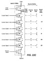
- Table 1 illustrates the function of polarity bits to convert a simple pattern to random pattern(s) across many wordlines. The randomization is achieved on the data located on the same NAND chain structure, an example of which is provided in FIG. 22C to illustrate this concept.
- FIG. 22C the lower and upper bits of a given cell are illustrated at each of the illustrated cells of the NAND string or chain.
- the NAND string shown is simply an example, and there may of course be more or less cells in a string, and structures different than that shown may be used with the present invention. For example, a cell storing 3, 4 or more bits may also be employed.
- the polarity bit preferably applies to a page or more of data, although application on the bit level is shown to illustrate the concept of bit inversion, especially in a multi state memory.
- the polarity bits are applied to each bit of the user data, and the resulting user data, as inverted or passed by the polarity bit, is labeled as the saved data.
- the saved data is the data that will subsequently be written to the memory array and stored as a result of the randomization operation. As can be seen, the states indicated at the right of the figure are defined by the upper and lower bit of the cell.
- the "saved data" terminology employed in FIG. 22C corresponds to what is referred to as the "User Data (UD) subsequent encoding” in Table 1 and FIG. 22 B.
- FIG. 23A illustrates another embodiment in which the register shown in FIG. 21 is a shift register with a feedback.
- the register 610 is configured as a pseudo-random generator. Its content is cyclically fed back to generate a sequence of pseudo random numbers. In this way, one bit will be used at a time, in contrast to the embodiment where all the bits of the code were used at a time.
- the shift register When a command is issued by a user, the shift register will shift to the next bit.
- the polarity bit used on the incoming user page will be from the last register output. This is preferably done on the rising edge of the command.
- the triggering command may be a program command, a cache program command, a read command, an erase command, or other user issued command.
- FIG. 23 B An example program command signal is shown in FIG. 23 B.
- the clock signal associated with the command is shown, and the instantiation of the command will be triggered by the user request, the timing and type of which is unpredictable and essentially random.
- FIG. 23A illustrates the clock signal associated with the user command as the one of the inputs that determines the polarity bit.
- the other input in the figure is the user data.
- the application of the polarity bit would invert or leave as is, the encoding of the data, as described previously.
- FIG. 23C illustrates an example of control circuitry for the data inversion.
- the data path with the single inverter will result in inverting of the encoding, whereas the path with the two inverters in series will result in the data encoding scheme being unaltered.
- the polarity bit associated with a group of data will be stored with that group of data. For example, as seen in FIG. 23D , for a page of data 630, the polarity bit 632 for the data in user area 636 would be programmed into the hidden area 634 of the page 630.
- the polarity bit 632 When the page 630 is read, the polarity bit 632 will be transferred out and latched to control the output data, and will revert the encoding scheme back if it was inverted, as accomplished by the exemplary circuitry shown in FIG. 23E . In this way, the polarity of the page will be reverted to its original encoding.
- the pattern of the code utilized by the shift register can vary and can be modified for different applications. If all bits are set to zero (in the case where zero indicates no change) then the randomization will be disabled. While the pattern of the bits in the register is pseudo random, the user behavior is unpredictable, and the resulting polarity at any given time is thus also unpredictable and random.
- Two examples of user behavior are as follows: 1) the user programs some pages and jumps to a different address to read or program some pages or to erase some blocks, then the returns back to the block where the last program occurred and continues to program more pages; and 2) the user programs all the pages sequentially without jumping to another address. In case 1, a new polarity bit can be triggered for each user command, whereas in case 2 the sequential programming will utilize and be based on one polarity bit.
- the final programmed data in the memory will likely be different for at least some of the various individual pages and groups of pages in these 2 cases.
- the EEPROM is typically controlled by a controller chip, and some of the actions of the "user" may be that of the controller chip.
- the polarity bit is also generated randomly as a result of a user command, such as the cache program operation described earlier.
- This embodiment utilizes two inputs that are not synchronized. The first is the timing of user commands, which as mentioned earlier is unpredictable. The second is a finite state machine clock. In certain memory systems, the finite state machine clock is only active at certain times (e.g. during cache operations), whereas in other systems it may always be active. This technique of this embodiment is available whenever the finite state machine clock of the memory system is active.
- the level or state of the finite state machine (“FSM”) clock is referenced.
- the state may be either high or low, as seen in FIG. 24A .
- a low state may correspond to a polarity bit of zero (although the opposite correspondence is also possible).
- the FSM is low and thus the polarity bit would be zero, indicating no change of the data encoding, as mentioned previously.
- the polarity bit 632 is loaded into the hidden area 634 as soon as the executing command is issued and it is sensed. In other embodiments it may be temporarily stored in another memory of the system.
- FIG. 24B illustrates an exemplary circuit to determine the polarity bit as described above. The inverter would again be preferably be rising edge triggered.
- FIG. 25 illustrates the On-chip control circuitry shown in FIG. 7A and FIG. 9 in more detail.
- the state machine 312 and the address decoder or generator 314 it also contains a data scrambler 318.
- it contains the register 610 and the multiplexer 614 shown in FIG. 21 and FIG. 23A .
- it also contains the data inverting circuit shown in FIG. 23C and the data reverting circuit shown in FIG. 23E .
- each page of data accessible by a common word line is programmed or read in parallel. Randomization on a page-by-page basis is accomplished by pseudo randomly selecting certain pages to have the polarity of their bits flipped.
- a repeated data pattern is stored into certain pages, either by a user or a controller, then the data may line up certain patterns which are detrimental to the boosting mode during programming for some NAND chain.
- the chains not to be programmed are program-inhibited by having their channel region boosted so as to reduce the effective programming voltage applied to the selected word line.
- a NAND type memory typically has each NAND chain programmed from the source side to the drain side.
- the data in the page is randomized such that when data from several pages are lined up problematic data patterns are avoided during programming.
- a simple way of scrambling the data on a page is to write the data on an independent or different starting address for each different page.
- a corresponding page of data is written to each page of memory cells at a different starting location for each page.
- the data is filled to the end of the page, it continues by wrapping around from the first address of the page until just before the starting location.
- FIG. 26 illustrates a method of scrambling the data on a memory page, according to one preferred embodiment of writing from different starting location for each page.
- FIG. 27 is a table illustrating an example of different pages having different starting locations for writing data. For example, on Page 0, byte 0 will be loaded starting from Column 0. On Page 1, byte 0 will be loaded starting from Column 1. The data will continue to load through Column n-1 and wrapped back to Column 0. In this example, each page has a designated shift to help misalign any repeated pattern in the data from page to page. In general, the starting column address is given as function of the page number. When the end of the physical column is reached, the data wraps around to the beginning of the physical column.
- the shifting of the starting column position for a given page is implemented by controlling the I/O circuits 440 shown in FIG. 9 .
- the address decoder 314 issues the starting address of the physical page to the I/O circuit in a data load operation. Data is clocked into the I/O circuit column by column according to the starting address. In the case of wrapping around, a second starting address is issued when the end of the physical column is reached.
- FIG. 23D illustrates the starting column address for each page can be stored in a portion of the page reserved for system use.
- the starting column address for page 630 is stored in a portion 634 of the memory array.
- a sequence of starting physical column addresses, one for each page, is provided by a pseudo-random generator such as that shown in FIG. 23A .
- Shifting the starting position of each page can avoid undesirable data patterns to line up within NAND chains and help to alleviate boosting problems during programming.
- scrambling of data within a page also helps to control the source loading error during sensing.
- the source loading errors are introduced by a finite resistance between the source line and the ground pad of the chip.
- One potential problem with sensing memory cells is source line bias caused by source loading across the finite resistance. When a large number of memory cells are sensed in parallel, their combined currents can result in significant voltage drop in a ground loop with finite resistance. This results in a source line bias which causes errors in a read operation employing threshold voltage sensing.
- FIG. 28A illustrates the problem of source voltage error due to current flow in the source line having a finite resistance to ground.
- the read/write circuits 370A and 370B operate on a page of memory cells simultaneously.
- Each sense modules 480 in the read/write circuits is coupled to a corresponding cell via a bit line 36.
- each sense module 480 includes a sense amplifier 212 connected to one of the bit lines, a set of data latches 430 and sharing the common processor 500 and I/O circuits 440. There will be a sense module for each of the memory cells in a page for parallel operation.
- a sense module 480 senses the conduction current i 1 (source-drain current) of a memory cell 10.
- the conduction current flows from the sense module through the bit line 36 into the drain of the memory cell 10 and out from the source 14 before going through a source line 34 to ground.
- the sources of the cells in a memory array are all tied together as multiple branches of the source line 34 connected to some external ground pad (e.g. Vss pad) of the memory chip.
- Vss pad some external ground pad
- each memory cell has a conduction current dependent on the amount of charge programmed into its charge storage element. For a given control gate voltage of the memory cell, a small charge will yield a comparatively higher conduction current (see FIG. 4 . )
- V drop i TOT R.
- the source line voltage drop will be equal to 64000 lines x 1 ⁇ A/line x 10 ohms ⁇ 0.64 volts.
- This source line bias will contribute to a sensing error of 0.96 volts when threshold voltages of the memory cells are sensed, assuming that the body effect is such that 0.64V rise in source voltage results in a 0.96V rise in threshold voltage.
- FIG. 28B illustrates the error in the threshold voltage level of a memory cell caused by a source line voltage drop.
- the threshold voltage V T supplied to the control gate 30 of the memory cell 10 is relative to GND.
- the effective V T seen by the memory cell is the voltage difference between its control gate 30 and source 14.
- There is a difference of approximately 1.5xV drop between the supplied and effective V T (ignoring the smaller contribution of voltage drop from the source 14 to the source line.)
- This V drop or source line bias will contribute to a sensing error of, for example, 0.96 volts when threshold voltages of the memory cells are sensed.
- the bias cannot be easily removed as it is data-dependent, i.e., dependent on the memory states of the memory cells of the page.
- the bias is highest in one extreme case when all the memory cells of the page are in the erased state. In this case, each cell is highly conductive, contributing to a large V drop and therefore a high source line bias. On the other hand, in the other extreme, when all the memory cells in the page are in the most programmed state, then each cell is non conductive, resulting in a minimum or no source line bias.
- the data bits in the page are randomized such that on average the page contains an equal mix of cells with erased and programmed states.
- the source line bias or loading does not vary substantially and can be allowed for with appropriate adjustment during the sensing operation.
- a sequence of pseudo random bits, each specifying a certain polarity is employed to encode bits within the page.
- FIG. 29 illustrates a method of randomizing bits within a page.
- the sequence of polarity bits, one for each set of data bits, is preferably provided by a pseudo-random generator such as that shown in FIG. 23A .
- Each set of data bits contains a predetermined number of bits.
- the predetermined number of bits is one.
- the predetermined number of bits is 8 bits.
- randomization within a page is combined with randomization form page to page.
- randomization within a page is preferably accomplished by each page having an independent starting position and randomization from page to page is preferably accomplished by each page having an independent encoding polarity.
- FIG. 30 illustrates a method of randomizing data page-by-page and within each page, according to another aspect of the invention.
- the data bits randomization within a page is also implemented by inserting STEP 760, STEP 762 and STEP 764 shown in FIG. 29 among STEP 810 to STEP 822.
- the bits in the word line direction and in the column direction are both randomized.
Landscapes
- Engineering & Computer Science (AREA)
- Computer Hardware Design (AREA)
- Read Only Memory (AREA)
- Techniques For Improving Reliability Of Storages (AREA)
Claims (15)
- Puce de mémoire à circuit intégré (600) comprenant une matrice de cellules de mémoire non volatile (602) accessibles page par page, chaque page représentant un groupe de cellules de mémoire, chaque cellule de mémoire du groupe étant dans une colonne de la matrice et le long d'une rangée accessible par une ligne de mots commune ;
caractérisée en ce que :une séquence de positions de colonnes de départ (figure 27) est délivrée de sorte que chaque page à programmer présente une position de colonne de départ associée ;un générateur d'adresses (figure 27) génère une adresse pour la position de colonne de départ associée ;un ensemble de circuits à verrouillage de données (430) est associé à chaque colonne en réponse au générateur d'adresses (314) en vue d'échelonner des données à programmer dans chaque page, les données échelonnées commençant à la position de colonne de départ associée et s'enroulant ainsi jusqu'à ce que la page soit remplie ; etun circuit de programmation (370) est apte à programmer en parallèle les données échelonnées dans chaque page. - Puce de mémoire selon la revendication 1, dans laquelle les pages sont numérotées consécutivement, et la position de colonne de départ associée à une page est en fonction du nombre des pages (figure 27).
- Puce de mémoire selon la revendication 2, dans laquelle la fonction est telle que la position de colonne est un modulo du nombre de cellules dans le groupe, à quoi s'ajoute un nombre prédéterminé.
- Puce de mémoire selon la revendication 1, comportant un générateur pseudo aléatoire (figure 23A) ; et dans laquelle la séquence de positions de colonnes de départ est générée sur la puce par le générateur pseudo aléatoire.
- Puce de mémoire selon la revendication 4, dans laquelle :le générateur pseudo aléatoire répond également à une temporisation déclenchée par un événement extérieur à la puce de mémoire (figures 24A et 24B) ; etla séquence de positions de colonnes de départ est également en fonction de la temporisation.
- Puce de mémoire selon l'une quelconque des revendications précédentes, comportant :des premier et second codages (tableau 1, figure 22B) pour chaque page de données à programmer, dans lequel le premier codage est destiné à laisser inchangé le bit de données associé à chaque colonne, et le second codage est destiné à basculer le bit de données ;une séquence de bits de polarité, un pour chaque page ; etun codeur (figure 23C) pour coder la page de données en utilisant le premier ou le second codage, selon que le bit de polarité de la page est dans un premier état ou un second état.
- Puce de mémoire selon l'une quelconque des revendications précédentes, dans laquelle les cellules de mémoire de la matrice sont agencées dans une architecture NON-ET (figure 1D, figure 3).
- Procédé mis en oeuvre dans une puce de mémoire à circuit intégré (600) comprenant une matrice de cellules de mémoire non volatile (602) accessibles page par page, chaque page représentant un groupe de cellules de mémoire, chaque cellule de mémoire du groupe étant dans une colonne de la matrice et le long d'une rangée accessible par une ligne de mots commune, le procédé étant destiné à programmer des données dans la matrice, et comprenant les étapes ci-dessous consistant à :générer sur la puce (770) une séquence de positions de colonnes de départ, de sorte que chaque page à programmer présente une position de colonne de départ associée ;échelonner des données (720, 822) à programmer dans chaque page, en commençant à la position de colonne de départ associée et en enroulant ainsi les données jusqu'à ce que la page soit remplie ; etprogrammer (730, 830) les données échelonnées en parallèle dans chaque page.
- Procédé selon la revendication 8, dans lequel les pages sont numérotées consécutivement, et la position de colonne de départ associée à une page est en fonction du nombre de pages.
- Procédé selon la revendication 9, dans lequel la fonction est telle que la position de colonne est un module du nombre de cellules dans le groupe, à quoi s'ajoute un nombre prédéterminé.
- Procédé selon la revendication 10, dans lequel le nombre prédéterminé est égal à zéro.
- Procédé selon la revendication 8, dans lequella séquence de positions de colonnes de départ est générée sur la puce par un générateur pseudo aléatoire (figure 23A).
- Procédé selon la revendication 12, dans lequel :le générateur pseudo aléatoire répond également à une temporisation déclenchée par un événement extérieur à la puce de mémoire (figures 24A et 24B) ; etla séquence de positions de colonnes de départ est également en fonction de la temporisation.
- Procédé selon la revendication 13, dans lequel l'événement externe est initié par un utilisateur de la puce de mémoire.
- Procédé selon l'une quelconque des revendications 8 à 14, comprenant en outre les étapes ci-dessous consistant à :fournir des premier et second codages (tableau 1, figure 22B) pour chaque page de données à programmer, dans lequel le premier codage est destiné à laisser inchangé le bit de données associé à chaque colonne, et le second codage est destiné à basculer le bit de données ;générer sur la puce une séquence de bits de polarité, un pour chaque page ; etcoder (figure 23C) la page de données en utilisant le premier ou le second codage, selon que le bit de polarité de la page est dans un premier état ou un second état.
Applications Claiming Priority (2)
| Application Number | Priority Date | Filing Date | Title |
|---|---|---|---|
| US11/852,229 US7885112B2 (en) | 2007-09-07 | 2007-09-07 | Nonvolatile memory and method for on-chip pseudo-randomization of data within a page and between pages |
| PCT/US2008/073750 WO2009035834A2 (fr) | 2007-09-07 | 2008-08-20 | Mémoire non volatile et procédé pour une distribution pseudo-aléatoire sur puce de données à l'intérieur d'une page et entre des pages |
Publications (2)
| Publication Number | Publication Date |
|---|---|
| EP2186094A2 EP2186094A2 (fr) | 2010-05-19 |
| EP2186094B1 true EP2186094B1 (fr) | 2012-03-14 |
Family
ID=40118001
Family Applications (1)
| Application Number | Title | Priority Date | Filing Date |
|---|---|---|---|
| EP08830722A Not-in-force EP2186094B1 (fr) | 2007-09-07 | 2008-08-20 | Mémoire non volatile et procédé pour une distribution pseudo-aléatoire sur puce de données à l'intérieur d'une page et entre des pages |
Country Status (8)
| Country | Link |
|---|---|
| US (1) | US7885112B2 (fr) |
| EP (1) | EP2186094B1 (fr) |
| JP (2) | JP5010031B2 (fr) |
| KR (1) | KR101533965B1 (fr) |
| CN (1) | CN102318007B (fr) |
| AT (1) | ATE549719T1 (fr) |
| TW (1) | TWI383396B (fr) |
| WO (1) | WO2009035834A2 (fr) |
Families Citing this family (55)
| Publication number | Priority date | Publication date | Assignee | Title |
|---|---|---|---|---|
| US7734861B2 (en) * | 2006-09-08 | 2010-06-08 | Sandisk Corporation | Pseudo random and command driven bit compensation for the cycling effects in flash memory |
| US7606966B2 (en) | 2006-09-08 | 2009-10-20 | Sandisk Corporation | Methods in a pseudo random and command driven bit compensation for the cycling effects in flash memory |
| US7764533B2 (en) * | 2007-09-18 | 2010-07-27 | International Business Machines Corporation | Multi-level memory cell utilizing measurement time delay as the characteristic parameter for level definition |
| JP5019611B2 (ja) * | 2007-12-27 | 2012-09-05 | 株式会社東芝 | メモリシステム |
| US8145855B2 (en) | 2008-09-12 | 2012-03-27 | Sandisk Technologies Inc. | Built in on-chip data scrambler for non-volatile memory |
| KR101082650B1 (ko) * | 2009-01-21 | 2011-11-14 | 주식회사 하이닉스반도체 | 불휘발성 메모리 장치 및 그 동작 방법 |
| KR20100099961A (ko) * | 2009-03-04 | 2010-09-15 | 삼성전자주식회사 | 불휘발성 메모리 장치 및 그 동작 방법 |
| KR101504338B1 (ko) * | 2009-03-04 | 2015-03-23 | 삼성전자주식회사 | 불휘발성 메모리 장치의 동작 방법 |
| KR20100124087A (ko) * | 2009-05-18 | 2010-11-26 | 삼성전자주식회사 | 메모리 컨트롤러, 그것을 포함하는 메모리 시스템 그리고 그것의 동작 방법 |
| US8102705B2 (en) | 2009-06-05 | 2012-01-24 | Sandisk Technologies Inc. | Structure and method for shuffling data within non-volatile memory devices |
| US20110002169A1 (en) | 2009-07-06 | 2011-01-06 | Yan Li | Bad Column Management with Bit Information in Non-Volatile Memory Systems |
| JP5321691B2 (ja) * | 2009-11-16 | 2013-10-23 | 富士通株式会社 | 並列計算装置、並列計算方法、および並列計算プログラム |
| KR20110055178A (ko) * | 2009-11-19 | 2011-05-25 | 삼성전자주식회사 | 플래시 메모리 장치 및 그것을 포함한 메모리 시스템 |
| US8495281B2 (en) * | 2009-12-04 | 2013-07-23 | International Business Machines Corporation | Intra-block memory wear leveling |
| US8144512B2 (en) * | 2009-12-18 | 2012-03-27 | Sandisk Technologies Inc. | Data transfer flows for on-chip folding |
| US8468294B2 (en) * | 2009-12-18 | 2013-06-18 | Sandisk Technologies Inc. | Non-volatile memory with multi-gear control using on-chip folding of data |
| US8725935B2 (en) | 2009-12-18 | 2014-05-13 | Sandisk Technologies Inc. | Balanced performance for on-chip folding of non-volatile memories |
| TWI438778B (zh) | 2010-03-25 | 2014-05-21 | Silicon Motion Inc | 用來抑制資料錯誤之方法以及相關之記憶裝置及其控制器 |
| KR20120002760A (ko) * | 2010-07-01 | 2012-01-09 | 삼성전자주식회사 | 낸드 플래쉬 메모리의 동작 신뢰성을 향상시키는 데이터 기록 방법 및 데이터 기록 장치 |
| US9342446B2 (en) | 2011-03-29 | 2016-05-17 | SanDisk Technologies, Inc. | Non-volatile memory system allowing reverse eviction of data updates to non-volatile binary cache |
| US8843693B2 (en) | 2011-05-17 | 2014-09-23 | SanDisk Technologies, Inc. | Non-volatile memory and method with improved data scrambling |
| US8762626B2 (en) | 2011-09-12 | 2014-06-24 | Sandisk Technologies Inc. | Data modification based on matching bit patterns |
| KR20130046190A (ko) * | 2011-10-27 | 2013-05-07 | 에스케이하이닉스 주식회사 | 반도체 메모리 장치 및 이의 동작 방법 |
| US8842473B2 (en) | 2012-03-15 | 2014-09-23 | Sandisk Technologies Inc. | Techniques for accessing column selecting shift register with skipped entries in non-volatile memories |
| US8681548B2 (en) | 2012-05-03 | 2014-03-25 | Sandisk Technologies Inc. | Column redundancy circuitry for non-volatile memory |
| US9292428B2 (en) * | 2012-09-05 | 2016-03-22 | Kabushiki Kaisha Toshiba | Memory system |
| US8897080B2 (en) | 2012-09-28 | 2014-11-25 | Sandisk Technologies Inc. | Variable rate serial to parallel shift register |
| US9076506B2 (en) | 2012-09-28 | 2015-07-07 | Sandisk Technologies Inc. | Variable rate parallel to serial shift register |
| US9490035B2 (en) | 2012-09-28 | 2016-11-08 | SanDisk Technologies, Inc. | Centralized variable rate serializer and deserializer for bad column management |
| TWI502597B (zh) * | 2013-05-13 | 2015-10-01 | Univ Nat Taiwan Science Tech | 非揮發性記憶體的資料反轉與回復方法 |
| KR102164630B1 (ko) | 2013-06-28 | 2020-10-12 | 삼성전자주식회사 | 메모리 컨트롤러 및 상기 메모리 컨트롤러의 동작 방법 |
| TWI527039B (zh) * | 2013-08-02 | 2016-03-21 | Toshiba Kk | Semiconductor memory device and data reading method |
| US9129701B2 (en) | 2013-12-19 | 2015-09-08 | Sandisk Technologies Inc. | Asymmetric state detection for non-volatile storage |
| US9576624B2 (en) | 2014-06-30 | 2017-02-21 | Seagate Technology Llc | Multi-dimentional data randomization |
| US9934872B2 (en) | 2014-10-30 | 2018-04-03 | Sandisk Technologies Llc | Erase stress and delta erase loop count methods for various fail modes in non-volatile memory |
| TWI566249B (zh) * | 2014-11-21 | 2017-01-11 | 慧榮科技股份有限公司 | 快閃記憶體的資料寫入方法與其控制裝置 |
| US9224502B1 (en) | 2015-01-14 | 2015-12-29 | Sandisk Technologies Inc. | Techniques for detection and treating memory hole to local interconnect marginality defects |
| US10032524B2 (en) | 2015-02-09 | 2018-07-24 | Sandisk Technologies Llc | Techniques for determining local interconnect defects |
| JP5940705B1 (ja) * | 2015-03-27 | 2016-06-29 | ウィンボンド エレクトロニクス コーポレーション | 半導体記憶装置 |
| US9269446B1 (en) | 2015-04-08 | 2016-02-23 | Sandisk Technologies Inc. | Methods to improve programming of slow cells |
| US9564219B2 (en) | 2015-04-08 | 2017-02-07 | Sandisk Technologies Llc | Current based detection and recording of memory hole-interconnect spacing defects |
| US10664343B2 (en) * | 2016-02-08 | 2020-05-26 | Sony Corporation | Memory controller, non-volatile memory, and method of controlling memory controller |
| KR102511459B1 (ko) * | 2016-03-17 | 2023-03-17 | 삼성전자주식회사 | 비휘발성 메모리 장치 및 그 동작 방법 |
| SG10201605746RA (en) * | 2016-07-13 | 2018-02-27 | Micron Technology Inc | Data storage with data randomizer in multiple operating modes |
| KR20190006760A (ko) * | 2017-07-11 | 2019-01-21 | 에스케이하이닉스 주식회사 | 반도체 메모리 장치 및 그것의 동작 방법 |
| US10319444B2 (en) | 2017-10-30 | 2019-06-11 | International Business Machines Corporation | Memory data randomizer |
| TWI660269B (zh) * | 2018-01-26 | 2019-05-21 | 慧榮科技股份有限公司 | 用來於一記憶裝置中進行寫入管理之方法以及記憶裝置及其控制器 |
| TWI709855B (zh) * | 2018-01-26 | 2020-11-11 | 慧榮科技股份有限公司 | 用來於一記憶裝置中進行寫入管理之方法以及記憶裝置及其控制器 |
| TWI641223B (zh) * | 2018-02-07 | 2018-11-11 | 大陸商北京集創北方科技股份有限公司 | Pseudo random bit sequence generation method and device, and integrated circuit generation system for generating pseudo random bit sequence generation device |
| US11012425B2 (en) | 2018-12-28 | 2021-05-18 | Micron Technology, Inc. | Replay protection nonce generation |
| US10937510B2 (en) | 2019-06-28 | 2021-03-02 | Western Digital Technologies, Inc. | Multidimensional pseudorandom binary sequence analysis for a memory device |
| JP2021140837A (ja) * | 2020-03-02 | 2021-09-16 | キオクシア株式会社 | 半導体記憶装置 |
| US11462278B2 (en) * | 2020-05-26 | 2022-10-04 | Samsung Electronics Co., Ltd. | Method and apparatus for managing seed value for data scrambling in NAND memory |
| US20220293188A1 (en) * | 2021-03-10 | 2022-09-15 | Sunrise Memory Corporation | Semiconductor memory device with write disturb reduction |
| US11462279B1 (en) * | 2021-05-13 | 2022-10-04 | Western Digital Technologies, Inc. | Modified distribution of memory device states |
Family Cites Families (66)
| Publication number | Priority date | Publication date | Assignee | Title |
|---|---|---|---|---|
| IT1224062B (it) * | 1979-09-28 | 1990-09-26 | Ates Componenti Elettron | Metodo di programmazione per una memoria a semiconduttore non volatile elettricamente alterabile |
| US5095344A (en) * | 1988-06-08 | 1992-03-10 | Eliyahou Harari | Highly compact eprom and flash eeprom devices |
| US4993029A (en) * | 1989-03-13 | 1991-02-12 | International Business Machines Corporation | Method and apparatus for randomizing data in a direct access storage device |
| US5070032A (en) * | 1989-03-15 | 1991-12-03 | Sundisk Corporation | Method of making dense flash eeprom semiconductor memory structures |
| US5172338B1 (en) * | 1989-04-13 | 1997-07-08 | Sandisk Corp | Multi-state eeprom read and write circuits and techniques |
| DE69033262T2 (de) * | 1989-04-13 | 2000-02-24 | Sandisk Corp | EEPROM-Karte mit Austauch von fehlerhaften Speicherzellen und Zwischenspeicher |
| US5343063A (en) * | 1990-12-18 | 1994-08-30 | Sundisk Corporation | Dense vertical programmable read only memory cell structure and processes for making them |
| JP3992757B2 (ja) * | 1991-04-23 | 2007-10-17 | テキサス インスツルメンツ インコーポレイテツド | マイクロプロセッサと同期するメモリ、及びデータプロセッサ、同期メモリ、周辺装置とシステムクロックを含むシステム |
| US6222762B1 (en) * | 1992-01-14 | 2001-04-24 | Sandisk Corporation | Multi-state memory |
| US5313421A (en) * | 1992-01-14 | 1994-05-17 | Sundisk Corporation | EEPROM with split gate source side injection |
| US5315541A (en) * | 1992-07-24 | 1994-05-24 | Sundisk Corporation | Segmented column memory array |
| US5555204A (en) * | 1993-06-29 | 1996-09-10 | Kabushiki Kaisha Toshiba | Non-volatile semiconductor memory device |
| KR0169267B1 (ko) * | 1993-09-21 | 1999-02-01 | 사토 후미오 | 불휘발성 반도체 기억장치 |
| JPH07228407A (ja) * | 1994-02-17 | 1995-08-29 | Shinko Electric Co Ltd | カード処理装置 |
| JPH07240098A (ja) | 1994-02-25 | 1995-09-12 | Sony Corp | 半導体不揮発性記憶装置 |
| US5661053A (en) * | 1994-05-25 | 1997-08-26 | Sandisk Corporation | Method of making dense flash EEPROM cell array and peripheral supporting circuits formed in deposited field oxide with the use of spacers |
| KR0172366B1 (ko) * | 1995-11-10 | 1999-03-30 | 김광호 | 불휘발성 반도체 메모리 장치의 독출 및 프로그램 방법과 그 회로 |
| JPH09204783A (ja) * | 1996-01-25 | 1997-08-05 | Sony Corp | 半導体不揮発性記憶装置 |
| US5903495A (en) * | 1996-03-18 | 1999-05-11 | Kabushiki Kaisha Toshiba | Semiconductor device and memory system |
| US5768192A (en) * | 1996-07-23 | 1998-06-16 | Saifun Semiconductors, Ltd. | Non-volatile semiconductor memory cell utilizing asymmetrical charge trapping |
| JPH10302490A (ja) * | 1997-04-25 | 1998-11-13 | Mitsubishi Electric Corp | 読み出し専用半導体記憶装置 |
| US6768165B1 (en) * | 1997-08-01 | 2004-07-27 | Saifun Semiconductors Ltd. | Two bit non-volatile electrically erasable and programmable semiconductor memory cell utilizing asymmetrical charge trapping |
| US6333871B1 (en) * | 1998-02-16 | 2001-12-25 | Hitachi, Ltd. | Nonvolatile semiconductor memory including a controller for providing an improved reprogram operation |
| JP3999900B2 (ja) * | 1998-09-10 | 2007-10-31 | 株式会社東芝 | 不揮発性半導体メモリ |
| EP1130600A1 (fr) | 2000-03-01 | 2001-09-05 | Hewlett-Packard Company, A Delaware Corporation | Schéma de distribution de données pour mémoires à l'état solide |
| JP3940544B2 (ja) * | 2000-04-27 | 2007-07-04 | 株式会社東芝 | 不揮発性半導体メモリのベリファイ方法 |
| US6266273B1 (en) * | 2000-08-21 | 2001-07-24 | Sandisk Corporation | Method and structure for reliable data copy operation for non-volatile memories |
| JP3829088B2 (ja) * | 2001-03-29 | 2006-10-04 | 株式会社東芝 | 半導体記憶装置 |
| US7549011B2 (en) * | 2001-08-30 | 2009-06-16 | Micron Technology, Inc. | Bit inversion in memory devices |
| JP3881869B2 (ja) * | 2001-11-05 | 2007-02-14 | 株式会社ルネサステクノロジ | 半導体記憶装置 |
| US6781877B2 (en) * | 2002-09-06 | 2004-08-24 | Sandisk Corporation | Techniques for reducing effects of coupling between storage elements of adjacent rows of memory cells |
| US6983428B2 (en) * | 2002-09-24 | 2006-01-03 | Sandisk Corporation | Highly compact non-volatile memory and method thereof |
| US7196931B2 (en) * | 2002-09-24 | 2007-03-27 | Sandisk Corporation | Non-volatile memory and method with reduced source line bias errors |
| US6657891B1 (en) * | 2002-11-29 | 2003-12-02 | Kabushiki Kaisha Toshiba | Semiconductor memory device for storing multivalued data |
| US7073103B2 (en) * | 2002-12-05 | 2006-07-04 | Sandisk Corporation | Smart verify for multi-state memories |
| US7237074B2 (en) * | 2003-06-13 | 2007-06-26 | Sandisk Corporation | Tracking cells for a memory system |
| US7173863B2 (en) * | 2004-03-08 | 2007-02-06 | Sandisk Corporation | Flash controller cache architecture |
| US7466590B2 (en) * | 2004-02-06 | 2008-12-16 | Sandisk Corporation | Self-boosting method for flash memory cells |
| CN101002279B (zh) * | 2004-03-26 | 2010-04-28 | 斯班逊有限公司 | 半导体器件及将资料写入该半导体器件的方法 |
| US7490283B2 (en) | 2004-05-13 | 2009-02-10 | Sandisk Corporation | Pipelined data relocation and improved chip architectures |
| US20060001400A1 (en) | 2004-06-30 | 2006-01-05 | Zedell Karl F | Battery charger with retention arms |
| US7274596B2 (en) * | 2004-06-30 | 2007-09-25 | Micron Technology, Inc. | Reduction of adjacent floating gate data pattern sensitivity |
| EP1622009A1 (fr) | 2004-07-27 | 2006-02-01 | Texas Instruments Incorporated | Architecture et systèmes JSM |
| US8375146B2 (en) * | 2004-08-09 | 2013-02-12 | SanDisk Technologies, Inc. | Ring bus structure and its use in flash memory systems |
| US7158421B2 (en) * | 2005-04-01 | 2007-01-02 | Sandisk Corporation | Use of data latches in multi-phase programming of non-volatile memories |
| US7120051B2 (en) * | 2004-12-14 | 2006-10-10 | Sandisk Corporation | Pipelined programming of non-volatile memories using early data |
| US7409473B2 (en) * | 2004-12-21 | 2008-08-05 | Sandisk Corporation | Off-chip data relocation |
| US7230851B2 (en) * | 2004-12-23 | 2007-06-12 | Sandisk Corporation | Reducing floating gate to floating gate coupling effect |
| US20060140007A1 (en) * | 2004-12-29 | 2006-06-29 | Raul-Adrian Cernea | Non-volatile memory and method with shared processing for an aggregate of read/write circuits |
| CN1838328A (zh) | 2005-01-19 | 2006-09-27 | 赛芬半导体有限公司 | 擦除存储器阵列上存储单元的方法 |
| US7251160B2 (en) * | 2005-03-16 | 2007-07-31 | Sandisk Corporation | Non-volatile memory and method with power-saving read and program-verify operations |
| WO2006107651A1 (fr) | 2005-04-01 | 2006-10-12 | Sandisk Corporation | Memoire a etats multiples possedant une recuperation de donnees apres un echec de programme |
| US7447078B2 (en) * | 2005-04-01 | 2008-11-04 | Sandisk Corporation | Method for non-volatile memory with background data latch caching during read operations |
| US7206230B2 (en) * | 2005-04-01 | 2007-04-17 | Sandisk Corporation | Use of data latches in cache operations of non-volatile memories |
| US7564713B2 (en) * | 2005-04-28 | 2009-07-21 | Kabushiki Kaisha Toshiba | Semiconductor integrated circuit device wherein during data write a potential transferred to each bit line is changed in accordance with program order of program data |
| US7203092B2 (en) * | 2005-05-12 | 2007-04-10 | Micron Technology, Inc. | Flash memory array using adjacent bit line as source |
| US7975304B2 (en) * | 2006-04-28 | 2011-07-05 | Trend Micro Incorporated | Portable storage device with stand-alone antivirus capability |
| US7558131B2 (en) * | 2006-05-18 | 2009-07-07 | Micron Technology, Inc. | NAND system with a data write frequency greater than a command-and-address-load frequency |
| WO2008031074A1 (fr) * | 2006-09-08 | 2008-03-13 | Sandisk Corporation | Compensation de bits pseudo-aléatoire et dirigée par la commande pour les effets de cycle en mémoire flash et ses procédés |
| US7734861B2 (en) * | 2006-09-08 | 2010-06-08 | Sandisk Corporation | Pseudo random and command driven bit compensation for the cycling effects in flash memory |
| US7606966B2 (en) * | 2006-09-08 | 2009-10-20 | Sandisk Corporation | Methods in a pseudo random and command driven bit compensation for the cycling effects in flash memory |
| US7489547B2 (en) * | 2006-12-29 | 2009-02-10 | Sandisk Corporation | Method of NAND flash memory cell array with adaptive memory state partitioning |
| JP4498370B2 (ja) * | 2007-02-14 | 2010-07-07 | 株式会社東芝 | データ書き込み方法 |
| JP2008217857A (ja) * | 2007-02-28 | 2008-09-18 | Toshiba Corp | メモリコントローラ及び半導体装置 |
| KR100857252B1 (ko) * | 2007-12-27 | 2008-09-05 | (주)인디링스 | 마모도를 비트 수준에서 평준화하는 플래시 메모리 장치 및플래시 메모리 프로그래밍 방법 |
| US8301912B2 (en) * | 2007-12-31 | 2012-10-30 | Sandisk Technologies Inc. | System, method and memory device providing data scrambling compatible with on-chip copy operation |
-
2007
- 2007-09-07 US US11/852,229 patent/US7885112B2/en active Active
-
2008
- 2008-08-20 WO PCT/US2008/073750 patent/WO2009035834A2/fr active Application Filing
- 2008-08-20 AT AT08830722T patent/ATE549719T1/de active
- 2008-08-20 JP JP2010524087A patent/JP5010031B2/ja not_active Expired - Fee Related
- 2008-08-20 CN CN200880115127.0A patent/CN102318007B/zh active Active
- 2008-08-20 KR KR1020107005088A patent/KR101533965B1/ko active IP Right Grant
- 2008-08-20 EP EP08830722A patent/EP2186094B1/fr not_active Not-in-force
- 2008-08-28 TW TW097132939A patent/TWI383396B/zh not_active IP Right Cessation
-
2012
- 2012-04-06 JP JP2012087398A patent/JP5537590B2/ja not_active Expired - Fee Related
Also Published As
| Publication number | Publication date |
|---|---|
| KR101533965B1 (ko) | 2015-07-06 |
| TW200929219A (en) | 2009-07-01 |
| CN102318007B (zh) | 2015-02-18 |
| US20090067244A1 (en) | 2009-03-12 |
| KR20100075833A (ko) | 2010-07-05 |
| WO2009035834A3 (fr) | 2009-05-22 |
| WO2009035834A2 (fr) | 2009-03-19 |
| US7885112B2 (en) | 2011-02-08 |
| TWI383396B (zh) | 2013-01-21 |
| JP5010031B2 (ja) | 2012-08-29 |
| JP2010538408A (ja) | 2010-12-09 |
| JP5537590B2 (ja) | 2014-07-02 |
| JP2012169034A (ja) | 2012-09-06 |
| ATE549719T1 (de) | 2012-03-15 |
| CN102318007A (zh) | 2012-01-11 |
| EP2186094A2 (fr) | 2010-05-19 |
Similar Documents
| Publication | Publication Date | Title |
|---|---|---|
| EP2186094B1 (fr) | Mémoire non volatile et procédé pour une distribution pseudo-aléatoire sur puce de données à l'intérieur d'une page et entre des pages | |
| US7734861B2 (en) | Pseudo random and command driven bit compensation for the cycling effects in flash memory | |
| EP1864289B1 (fr) | Utilisation de verrous de donnees dans des operations de cache de memoire non volatile | |
| EP2070090B1 (fr) | Compensation de bits pseudo-aléatoire et dirigée par la commande pour les effets de cycle en mémoire flash et ses procédés | |
| JP4814995B2 (ja) | 読み出し操作中にデータラッチでバックグラウンドキャッシングを行う不揮発性メモリとその方法 | |
| EP1869681B1 (fr) | Utilisation de verrouillages de donnees dans la programmation a phases multiples de memoires non volatiles | |
| US7606966B2 (en) | Methods in a pseudo random and command driven bit compensation for the cycling effects in flash memory | |
| US7345928B2 (en) | Data recovery methods in multi-state memory after program fail | |
| US8873303B2 (en) | Non-volatile memory and method with shared processing for an aggregate of read/write circuits | |
| WO2006107651A1 (fr) | Memoire a etats multiples possedant une recuperation de donnees apres un echec de programme |
Legal Events
| Date | Code | Title | Description |
|---|---|---|---|
| PUAI | Public reference made under article 153(3) epc to a published international application that has entered the european phase |
Free format text: ORIGINAL CODE: 0009012 |
|
| 17P | Request for examination filed |
Effective date: 20100302 |
|
| AK | Designated contracting states |
Kind code of ref document: A2 Designated state(s): AT BE BG CH CY CZ DE DK EE ES FI FR GB GR HR HU IE IS IT LI LT LU LV MC MT NL NO PL PT RO SE SI SK TR |
|
| AX | Request for extension of the european patent |
Extension state: AL BA MK RS |
|
| 17Q | First examination report despatched |
Effective date: 20100721 |
|
| GRAP | Despatch of communication of intention to grant a patent |
Free format text: ORIGINAL CODE: EPIDOSNIGR1 |
|
| DAX | Request for extension of the european patent (deleted) | ||
| GRAS | Grant fee paid |
Free format text: ORIGINAL CODE: EPIDOSNIGR3 |
|
| GRAA | (expected) grant |
Free format text: ORIGINAL CODE: 0009210 |
|
| AK | Designated contracting states |
Kind code of ref document: B1 Designated state(s): AT BE BG CH CY CZ DE DK EE ES FI FR GB GR HR HU IE IS IT LI LT LU LV MC MT NL NO PL PT RO SE SI SK TR |
|
| REG | Reference to a national code |
Ref country code: GB Ref legal event code: FG4D |
|
| REG | Reference to a national code |
Ref country code: AT Ref legal event code: REF Ref document number: 549719 Country of ref document: AT Kind code of ref document: T Effective date: 20120315 Ref country code: CH Ref legal event code: EP |
|
| RAP2 | Party data changed (patent owner data changed or rights of a patent transferred) |
Owner name: SANDISK TECHNOLOGIES INC. |
|
| REG | Reference to a national code |
Ref country code: IE Ref legal event code: FG4D |
|
| REG | Reference to a national code |
Ref country code: DE Ref legal event code: R096 Ref document number: 602008014167 Country of ref document: DE Effective date: 20120510 |
|
| REG | Reference to a national code |
Ref country code: NL Ref legal event code: T3 |
|
| PG25 | Lapsed in a contracting state [announced via postgrant information from national office to epo] |
Ref country code: LT Free format text: LAPSE BECAUSE OF FAILURE TO SUBMIT A TRANSLATION OF THE DESCRIPTION OR TO PAY THE FEE WITHIN THE PRESCRIBED TIME-LIMIT Effective date: 20120314 Ref country code: HR Free format text: LAPSE BECAUSE OF FAILURE TO SUBMIT A TRANSLATION OF THE DESCRIPTION OR TO PAY THE FEE WITHIN THE PRESCRIBED TIME-LIMIT Effective date: 20120314 Ref country code: NO Free format text: LAPSE BECAUSE OF FAILURE TO SUBMIT A TRANSLATION OF THE DESCRIPTION OR TO PAY THE FEE WITHIN THE PRESCRIBED TIME-LIMIT Effective date: 20120614 |
|
| LTIE | Lt: invalidation of european patent or patent extension |
Effective date: 20120314 |
|
| PG25 | Lapsed in a contracting state [announced via postgrant information from national office to epo] |
Ref country code: FI Free format text: LAPSE BECAUSE OF FAILURE TO SUBMIT A TRANSLATION OF THE DESCRIPTION OR TO PAY THE FEE WITHIN THE PRESCRIBED TIME-LIMIT Effective date: 20120314 Ref country code: LV Free format text: LAPSE BECAUSE OF FAILURE TO SUBMIT A TRANSLATION OF THE DESCRIPTION OR TO PAY THE FEE WITHIN THE PRESCRIBED TIME-LIMIT Effective date: 20120314 Ref country code: GR Free format text: LAPSE BECAUSE OF FAILURE TO SUBMIT A TRANSLATION OF THE DESCRIPTION OR TO PAY THE FEE WITHIN THE PRESCRIBED TIME-LIMIT Effective date: 20120615 |
|
| REG | Reference to a national code |
Ref country code: AT Ref legal event code: MK05 Ref document number: 549719 Country of ref document: AT Kind code of ref document: T Effective date: 20120314 |
|
| PG25 | Lapsed in a contracting state [announced via postgrant information from national office to epo] |
Ref country code: CY Free format text: LAPSE BECAUSE OF FAILURE TO SUBMIT A TRANSLATION OF THE DESCRIPTION OR TO PAY THE FEE WITHIN THE PRESCRIBED TIME-LIMIT Effective date: 20120314 |
|
| PG25 | Lapsed in a contracting state [announced via postgrant information from national office to epo] |
Ref country code: RO Free format text: LAPSE BECAUSE OF FAILURE TO SUBMIT A TRANSLATION OF THE DESCRIPTION OR TO PAY THE FEE WITHIN THE PRESCRIBED TIME-LIMIT Effective date: 20120314 Ref country code: PL Free format text: LAPSE BECAUSE OF FAILURE TO SUBMIT A TRANSLATION OF THE DESCRIPTION OR TO PAY THE FEE WITHIN THE PRESCRIBED TIME-LIMIT Effective date: 20120314 Ref country code: SI Free format text: LAPSE BECAUSE OF FAILURE TO SUBMIT A TRANSLATION OF THE DESCRIPTION OR TO PAY THE FEE WITHIN THE PRESCRIBED TIME-LIMIT Effective date: 20120314 Ref country code: SE Free format text: LAPSE BECAUSE OF FAILURE TO SUBMIT A TRANSLATION OF THE DESCRIPTION OR TO PAY THE FEE WITHIN THE PRESCRIBED TIME-LIMIT Effective date: 20120314 Ref country code: IS Free format text: LAPSE BECAUSE OF FAILURE TO SUBMIT A TRANSLATION OF THE DESCRIPTION OR TO PAY THE FEE WITHIN THE PRESCRIBED TIME-LIMIT Effective date: 20120714 Ref country code: BE Free format text: LAPSE BECAUSE OF FAILURE TO SUBMIT A TRANSLATION OF THE DESCRIPTION OR TO PAY THE FEE WITHIN THE PRESCRIBED TIME-LIMIT Effective date: 20120314 Ref country code: EE Free format text: LAPSE BECAUSE OF FAILURE TO SUBMIT A TRANSLATION OF THE DESCRIPTION OR TO PAY THE FEE WITHIN THE PRESCRIBED TIME-LIMIT Effective date: 20120314 Ref country code: CZ Free format text: LAPSE BECAUSE OF FAILURE TO SUBMIT A TRANSLATION OF THE DESCRIPTION OR TO PAY THE FEE WITHIN THE PRESCRIBED TIME-LIMIT Effective date: 20120314 |
|
| PG25 | Lapsed in a contracting state [announced via postgrant information from national office to epo] |
Ref country code: PT Free format text: LAPSE BECAUSE OF FAILURE TO SUBMIT A TRANSLATION OF THE DESCRIPTION OR TO PAY THE FEE WITHIN THE PRESCRIBED TIME-LIMIT Effective date: 20120716 Ref country code: SK Free format text: LAPSE BECAUSE OF FAILURE TO SUBMIT A TRANSLATION OF THE DESCRIPTION OR TO PAY THE FEE WITHIN THE PRESCRIBED TIME-LIMIT Effective date: 20120314 |
|
| PLBE | No opposition filed within time limit |
Free format text: ORIGINAL CODE: 0009261 |
|
| STAA | Information on the status of an ep patent application or granted ep patent |
Free format text: STATUS: NO OPPOSITION FILED WITHIN TIME LIMIT |
|
| PG25 | Lapsed in a contracting state [announced via postgrant information from national office to epo] |
Ref country code: DK Free format text: LAPSE BECAUSE OF FAILURE TO SUBMIT A TRANSLATION OF THE DESCRIPTION OR TO PAY THE FEE WITHIN THE PRESCRIBED TIME-LIMIT Effective date: 20120314 Ref country code: AT Free format text: LAPSE BECAUSE OF FAILURE TO SUBMIT A TRANSLATION OF THE DESCRIPTION OR TO PAY THE FEE WITHIN THE PRESCRIBED TIME-LIMIT Effective date: 20120314 |
|
| 26N | No opposition filed |
Effective date: 20121217 |
|
| PG25 | Lapsed in a contracting state [announced via postgrant information from national office to epo] |
Ref country code: IT Free format text: LAPSE BECAUSE OF FAILURE TO SUBMIT A TRANSLATION OF THE DESCRIPTION OR TO PAY THE FEE WITHIN THE PRESCRIBED TIME-LIMIT Effective date: 20120314 |
|
| REG | Reference to a national code |
Ref country code: CH Ref legal event code: PL |
|
| PG25 | Lapsed in a contracting state [announced via postgrant information from national office to epo] |
Ref country code: MC Free format text: LAPSE BECAUSE OF NON-PAYMENT OF DUE FEES Effective date: 20120831 |
|
| REG | Reference to a national code |
Ref country code: DE Ref legal event code: R097 Ref document number: 602008014167 Country of ref document: DE Effective date: 20121217 |
|
| PG25 | Lapsed in a contracting state [announced via postgrant information from national office to epo] |
Ref country code: CH Free format text: LAPSE BECAUSE OF NON-PAYMENT OF DUE FEES Effective date: 20120831 Ref country code: LI Free format text: LAPSE BECAUSE OF NON-PAYMENT OF DUE FEES Effective date: 20120831 Ref country code: ES Free format text: LAPSE BECAUSE OF FAILURE TO SUBMIT A TRANSLATION OF THE DESCRIPTION OR TO PAY THE FEE WITHIN THE PRESCRIBED TIME-LIMIT Effective date: 20120625 |
|
| REG | Reference to a national code |
Ref country code: IE Ref legal event code: MM4A |
|
| PG25 | Lapsed in a contracting state [announced via postgrant information from national office to epo] |
Ref country code: BG Free format text: LAPSE BECAUSE OF FAILURE TO SUBMIT A TRANSLATION OF THE DESCRIPTION OR TO PAY THE FEE WITHIN THE PRESCRIBED TIME-LIMIT Effective date: 20120614 Ref country code: IE Free format text: LAPSE BECAUSE OF NON-PAYMENT OF DUE FEES Effective date: 20120820 |
|
| PGFP | Annual fee paid to national office [announced via postgrant information from national office to epo] |
Ref country code: NL Payment date: 20130810 Year of fee payment: 6 |
|
| PG25 | Lapsed in a contracting state [announced via postgrant information from national office to epo] |
Ref country code: MT Free format text: LAPSE BECAUSE OF FAILURE TO SUBMIT A TRANSLATION OF THE DESCRIPTION OR TO PAY THE FEE WITHIN THE PRESCRIBED TIME-LIMIT Effective date: 20120314 |
|
| PGFP | Annual fee paid to national office [announced via postgrant information from national office to epo] |
Ref country code: FR Payment date: 20130808 Year of fee payment: 6 |
|
| PG25 | Lapsed in a contracting state [announced via postgrant information from national office to epo] |
Ref country code: TR Free format text: LAPSE BECAUSE OF FAILURE TO SUBMIT A TRANSLATION OF THE DESCRIPTION OR TO PAY THE FEE WITHIN THE PRESCRIBED TIME-LIMIT Effective date: 20120314 |
|
| PG25 | Lapsed in a contracting state [announced via postgrant information from national office to epo] |
Ref country code: LU Free format text: LAPSE BECAUSE OF NON-PAYMENT OF DUE FEES Effective date: 20120820 |
|
| PG25 | Lapsed in a contracting state [announced via postgrant information from national office to epo] |
Ref country code: HU Free format text: LAPSE BECAUSE OF FAILURE TO SUBMIT A TRANSLATION OF THE DESCRIPTION OR TO PAY THE FEE WITHIN THE PRESCRIBED TIME-LIMIT Effective date: 20080820 |
|
| REG | Reference to a national code |
Ref country code: NL Ref legal event code: V1 Effective date: 20150301 |
|
| PG25 | Lapsed in a contracting state [announced via postgrant information from national office to epo] |
Ref country code: NL Free format text: LAPSE BECAUSE OF NON-PAYMENT OF DUE FEES Effective date: 20150301 |
|
| REG | Reference to a national code |
Ref country code: FR Ref legal event code: ST Effective date: 20150430 |
|
| PG25 | Lapsed in a contracting state [announced via postgrant information from national office to epo] |
Ref country code: FR Free format text: LAPSE BECAUSE OF NON-PAYMENT OF DUE FEES Effective date: 20140901 |
|
| PGFP | Annual fee paid to national office [announced via postgrant information from national office to epo] |
Ref country code: GB Payment date: 20180815 Year of fee payment: 11 |
|
| GBPC | Gb: european patent ceased through non-payment of renewal fee |
Effective date: 20190820 |
|
| PG25 | Lapsed in a contracting state [announced via postgrant information from national office to epo] |
Ref country code: GB Free format text: LAPSE BECAUSE OF NON-PAYMENT OF DUE FEES Effective date: 20190820 |
|
| PGFP | Annual fee paid to national office [announced via postgrant information from national office to epo] |
Ref country code: DE Payment date: 20220608 Year of fee payment: 15 |
|
| P01 | Opt-out of the competence of the unified patent court (upc) registered |
Effective date: 20230606 |
|
| REG | Reference to a national code |
Ref country code: DE Ref legal event code: R119 Ref document number: 602008014167 Country of ref document: DE |