US10120792B1 - Programming an embedded flash storage device - Google Patents
Programming an embedded flash storage device Download PDFInfo
- Publication number
- US10120792B1 US10120792B1 US14/167,879 US201414167879A US10120792B1 US 10120792 B1 US10120792 B1 US 10120792B1 US 201414167879 A US201414167879 A US 201414167879A US 10120792 B1 US10120792 B1 US 10120792B1
- Authority
- US
- United States
- Prior art keywords
- flash memory
- storage device
- embedded
- recovery metadata
- unit
- Prior art date
- Legal status (The legal status is an assumption and is not a legal conclusion. Google has not performed a legal analysis and makes no representation as to the accuracy of the status listed.)
- Active, expires
Links
Images


Classifications
-
- G—PHYSICS
- G06—COMPUTING; CALCULATING OR COUNTING
- G06F—ELECTRIC DIGITAL DATA PROCESSING
- G06F12/00—Accessing, addressing or allocating within memory systems or architectures
- G06F12/02—Addressing or allocation; Relocation
- G06F12/0223—User address space allocation, e.g. contiguous or non contiguous base addressing
- G06F12/023—Free address space management
- G06F12/0238—Memory management in non-volatile memory, e.g. resistive RAM or ferroelectric memory
- G06F12/0246—Memory management in non-volatile memory, e.g. resistive RAM or ferroelectric memory in block erasable memory, e.g. flash memory
-
- G—PHYSICS
- G06—COMPUTING; CALCULATING OR COUNTING
- G06F—ELECTRIC DIGITAL DATA PROCESSING
- G06F3/00—Input arrangements for transferring data to be processed into a form capable of being handled by the computer; Output arrangements for transferring data from processing unit to output unit, e.g. interface arrangements
- G06F3/06—Digital input from, or digital output to, record carriers, e.g. RAID, emulated record carriers or networked record carriers
- G06F3/0601—Interfaces specially adapted for storage systems
- G06F3/0602—Interfaces specially adapted for storage systems specifically adapted to achieve a particular effect
- G06F3/061—Improving I/O performance
- G06F3/0611—Improving I/O performance in relation to response time
-
- G—PHYSICS
- G06—COMPUTING; CALCULATING OR COUNTING
- G06F—ELECTRIC DIGITAL DATA PROCESSING
- G06F2212/00—Indexing scheme relating to accessing, addressing or allocation within memory systems or architectures
- G06F2212/10—Providing a specific technical effect
- G06F2212/1016—Performance improvement
- G06F2212/1024—Latency reduction
-
- G—PHYSICS
- G06—COMPUTING; CALCULATING OR COUNTING
- G06F—ELECTRIC DIGITAL DATA PROCESSING
- G06F2212/00—Indexing scheme relating to accessing, addressing or allocation within memory systems or architectures
- G06F2212/72—Details relating to flash memory management
- G06F2212/7201—Logical to physical mapping or translation of blocks or pages
-
- G—PHYSICS
- G06—COMPUTING; CALCULATING OR COUNTING
- G06F—ELECTRIC DIGITAL DATA PROCESSING
- G06F2212/00—Indexing scheme relating to accessing, addressing or allocation within memory systems or architectures
- G06F2212/72—Details relating to flash memory management
- G06F2212/7207—Details relating to flash memory management management of metadata or control data
-
- G—PHYSICS
- G06—COMPUTING; CALCULATING OR COUNTING
- G06F—ELECTRIC DIGITAL DATA PROCESSING
- G06F3/00—Input arrangements for transferring data to be processed into a form capable of being handled by the computer; Output arrangements for transferring data from processing unit to output unit, e.g. interface arrangements
- G06F3/06—Digital input from, or digital output to, record carriers, e.g. RAID, emulated record carriers or networked record carriers
- G06F3/0601—Interfaces specially adapted for storage systems
- G06F3/0628—Interfaces specially adapted for storage systems making use of a particular technique
- G06F3/0655—Vertical data movement, i.e. input-output transfer; data movement between one or more hosts and one or more storage devices
- G06F3/0659—Command handling arrangements, e.g. command buffers, queues, command scheduling
-
- G—PHYSICS
- G06—COMPUTING; CALCULATING OR COUNTING
- G06F—ELECTRIC DIGITAL DATA PROCESSING
- G06F3/00—Input arrangements for transferring data to be processed into a form capable of being handled by the computer; Output arrangements for transferring data from processing unit to output unit, e.g. interface arrangements
- G06F3/06—Digital input from, or digital output to, record carriers, e.g. RAID, emulated record carriers or networked record carriers
- G06F3/0601—Interfaces specially adapted for storage systems
- G06F3/0668—Interfaces specially adapted for storage systems adopting a particular infrastructure
- G06F3/0671—In-line storage system
- G06F3/0673—Single storage device
- G06F3/0679—Non-volatile semiconductor memory device, e.g. flash memory, one time programmable memory [OTP]
Abstract
A method that includes sending to an embedded flash storage device (EFSD) and during a transaction, a data unit and recovery metadata that differs from a flash memory unit memory management data structure (FMUMMDS); instructing the EFSD to program the data unit and the recovery metadata to a group of flash memory cells; sending to the host computer a transaction completion indication in response to a successful completion of the programming and before a completion of a management process that comprises updating by the flash memory controller, the FMUMMDS to reflect (a) the recovery metadata and (b) physical address information related to the group of the flash memory cells; and programming, by the EFSD, the FMUMMDS to the flash memory unit; wherein the data structure is reconstructible based upon the recovery metadata and the physical address information related to the group of the flash memory cells.
Description
An embedded flash storage device (such as an embedded flash storage device) is a flash storage device that is embedded in a computerized system that also includes a host computer and a flash memory controller. The embedded flash storage device may be activated only under the permission of the host computer.
Data units can be read from the embedded flash storage device during read transactions and can be written (programmed) to the embedded flash storage device during write transactions.
The read and write processes utilize one or more memory management tables that may map logical addresses of data units to physical addresses of flash memory cells that store the data units.
The embedded flash storage device are subjected to power failures but are expected to maintain the integrity of data units that were written during successfully completed write transactions despite such power failures.
In order to maintain this integrity a successfully completed write transaction should include the programming of (a) data unit, and of (b) one or more memory management tables that are updated to reflect the programming of the data unit.
The throughput of an embedded flash storage device is inversely proportional to the latency of a transaction.
Referring to a write transaction latency—this latency is defined by a period required to successfully complete a write transaction—including a programming of one or more data units and a programming updated memory management tables (after updating the memory management tables).
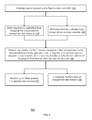
The method 20 includes the following sequence of stages starting (21) by a flash memory controller, a write transaction; programming (22), by the embedded flash storage device, a data unit to a flash memory unit of the embedded flash storage device; updating (23) by the flash memory controller, the memory management tables to reflect the programming of the data unit; programming (24) by the embedded flash storage device, the memory management tables (after being updated) to the flash memory unit; sending (25) to the host computer an acknowledgement of a successful completion of the write transaction—after a successful completion of stages 21-24; sending (26) the write transaction.
It is noted that stages 22 and 24 are relatively long in relation to other stages of method 20.
Timing diagram 10 illustrates the sequence of signals and stages a write transaction initialization signal 11 from the host computer to the flash memory controller. This starts a write transaction of duration 12; initial operations (13) executed by the flash memory controller before the programming of a data unit. This may include determining where to write the data unit, error correction encoding the data unit and the like; programming (14) by the embedded flash storage device, a data unit to the flash memory unit of the embedded flash storage device; intermediate operations (15) executed by the flash memory controller before programming the memory management tables—such as updating the memory management tables; programming (16) the memory management tables to the flash memory unit; final operations (17) executed by the flash memory controller. For example—checking the status of a program; sending (18) an acknowledgment to the host computer and thereby ending the transaction.
As illustrated above—the host computer can be notified that the write transaction succeeded only after the (entire) write transaction succeeded and thus the latency of write transaction is relatively high and the throughput of the embedded flash is low.
There is a need to provide a low latency and power failure tolerant method for programming data units to an embedded flash storage device.
According to an embodiment of the invention a method may be provided and may include sending, by a flash memory controller, to an embedded flash storage device and during a transaction, a data unit and recovery metadata; wherein the recovery metadata differs from a flash memory unit memory management data structure; instructing the embedded flash storage device to program the data unit and the recovery metadata to a group of flash memory cells of a flash memory unit of the embedded flash storage device; sending, by the flash memory controller, to the host computer a transaction completion indication in response to a successful completion of the programming and before a completion of a management process that may include updating by the flash memory controller, the flash memory unit management data structure to reflect (a) the recovery metadata and (b) physical address information related to the group of the flash memory cells; and programming, by the embedded flash storage device, the flash memory management data structure to the flash memory unit; wherein the flash memory management data structure is reconstructible based upon the recovery metadata and the physical address information related to the group of the flash memory cells.
The method may include attempting by the embedded flash storage device to complete the management process.
The management process is assigned a lower priority than programming data units to the flash memory unit.
The method may include reconstructing, by the flash memory controller, the flash memory management data structure based upon the recovery metadata and the physical address information related to the group of the flash memory cells if the management process failed to be successfully completed. The failure may be contributed to a sudden power drop.
The method may include determining, by the flash memory controller, whether the management process failed by comparing (a) a content of a flash memory management data structure stored in the flash memory unit and (b) a combination of (i) the recovery metadata and (ii) the physical address information related to the group of the flash memory cells.
The method may include determining, by the flash memory controller, whether the management process failed by comparing (a) a first mapping between a logical address and a physical address of the data unit as reflected by a flash memory management data structure stored in the flash memory unit and (b) a second mapping between the logical address and the physical address of the data unit as reflected by the recovery metadata and the physical address information related to the group of the flash memory cells.
The method may include updating the flash memory unit management data structure in parallel to a programming of the data unit and the recovery metadata by the embedded flash storage device.
The method may include receiving multiple data units and performing multiple updates of the flash memory management data structure, each update related to a different data unit of the multiple data units to provide the flash memory management data structure before programming the flash memory management data structure to the flash memory unit.
The recovery metadata may represent a logical address of the data unit.
According to an embodiment of the invention there may be provided a non-transitory computer readable medium that includes instructions to be executed by a computerized system and may store instructions for sending to an embedded flash storage device and during a transaction, a data unit and recovery metadata; wherein the recovery metadata differs from a flash memory unit memory management data structure; instructing the embedded flash storage device to program the data unit and the recovery metadata to a group of flash memory cells of a flash memory unit of the embedded flash storage device; sending to the host computer a transaction completion indication in response to a successful completion of the programming and before a completion of a management process that may include updating the flash memory unit management data structure to reflect (a) the recovery metadata and (b) physical address information related to the group of the flash memory cells; and programming, by the embedded flash storage device, the flash memory management data structure to the flash memory unit; wherein the flash memory management data structure is reconstructible based upon the recovery metadata and the physical address information related to the group of the flash memory cells.
The non-transitory computer readable medium may store instructions for attempting by the embedded flash storage device to complete the management process.
The management process is assigned a lower priority than programming data units to the flash memory unit.
The non-transitory computer readable medium may store instructions for reconstructing, by the flash memory controller, the flash memory management data structure based upon the recovery metadata and the physical address information related to the group of the flash memory cells if the management process failed to be successfully completed.
The non-transitory computer readable medium may store instructions for determining, by the flash memory controller, whether the management process failed by comparing (a) a content of a flash memory management data structure stored in the flash memory unit and (b) a combination of (i) the recovery metadata and (ii) the physical address information related to the group of the flash memory cells.
The non-transitory computer readable medium may store instructions for determining, by the flash memory controller, whether the management process failed by comparing (a) a first mapping between a logical address and a physical address of the data unit as reflected by a flash memory management data structure stored in the flash memory unit and (b) a second mapping between the logical address and the physical address of the data unit as reflected by the recovery metadata and the physical address information related to the group of the flash memory cells.
The non-transitory computer readable medium may store instructions for updating the flash memory unit management data structure in parallel to a programming of the data unit and the recovery metadata by the embedded flash storage device.
The non-transitory computer readable medium may store instructions for receiving multiple data units and performing multiple updates of the flash memory management data structure, each update related to a different data unit of the multiple data units to provide the flash memory management data structure before programming the flash memory management data structure to the flash memory unit.
The recovery metadata represents a logical address of the data unit.
According to an embodiment of the invention there may be provided a flash memory controller, may include a write circuit that is arranged to send to embedded flash storage device and during a transaction, a data unit and recovery metadata; wherein the recovery metadata differs from a flash memory unit memory management data structure; instruct the embedded flash storage device to program the data unit and the recovery metadata to a group of flash memory cells of a flash memory unit of the embedded flash storage device; and an interface that is arranged to send to a host computer a transaction completion indication in response to a successful completion of the programming and before a completion of management process that may include updating the flash memory unit management data structure to reflect (a) the recovery metadata and (b) physical address information related to the group of the flash memory cells; and programming, by the embedded flash storage device, the flash memory management data structure to the flash memory unit; wherein the flash memory management data structure is reconstructible based upon the recovery metadata and the physical address information related to the group of the flash memory cells.
The flash memory controller may include a random access memory for storing the flash memory management data structure.
The flash memory controller may be arranged to attempt to complete the management process.
The management process may be assigned a lower priority than programming data units to the flash memory unit.
The flash memory controller may be arranged to reconstruct the flash memory management data structure based upon the recovery metadata and the physical address information related to the group of the flash memory cells if the management process failed to be successfully completed. The failure may be contributed to a sudden power drop.
The flash memory controller may be arranged to determine whether the management process failed by comparing (a) a content of a flash memory management data structure stored in the flash memory unit and (b) a combination of (i) the recovery metadata and (ii) the physical address information related to the group of the flash memory cells.
The flash memory controller may be arranged to determine whether the management process failed by comparing (a) a first mapping between a logical address and a physical address of the data unit as reflected by a flash memory management data structure stored in the flash memory unit and (b) a second mapping between the logical address and the physical address of the data unit as reflected by the recovery metadata and the physical address information related to the group of the flash memory cells.
The flash memory controller may be arranged to update the flash memory unit management data structure in parallel to a programming of the data unit and the recovery metadata by the embedded flash storage device.
The flash memory controller may be arranged to receive multiple data units and performing multiple updates of the flash memory management data structure, each update related to a different data unit of the multiple data units to provide the flash memory management data structure before programming the flash memory management data structure to the flash memory unit.
The recovery metadata may represent a logical address of the data unit.
The subject matter regarded as the invention is particularly pointed out and distinctly claimed in the concluding portion of the specification. The invention, however, both as to organization and method of operation, together with objects, features, and advantages thereof, may best be understood by reference to the following detailed description when read with the accompanying drawings in which:
It will be appreciated that for simplicity and clarity of illustration, elements shown in the figures have not necessarily been drawn to scale. For example, the dimensions of some of the elements may be exaggerated relative to other elements for clarity. Further, where considered appropriate, reference numerals may be repeated among the figures to indicate corresponding or analogous elements.
In the following detailed description, numerous specific details are set forth in order to provide a thorough understanding of the invention. However, it will be understood by those skilled in the art that the present invention may be practiced without these specific details. In other instances, well-known methods, procedures, and components have not been described in detail so as not to obscure the present invention.
The subject matter regarded as the invention is particularly pointed out and distinctly claimed in the concluding portion of the specification. The invention, however, both as to organization and method of operation, together with objects, features, and advantages thereof, may best be understood by reference to the following detailed description when read with the accompanying drawings.
Because the illustrated embodiments of the present invention may for the most part, be implemented using electronic components and circuits known to those skilled in the art, details will not be explained in any greater extent than that considered necessary as illustrated above, for the understanding and appreciation of the underlying concepts of the present invention and in order not to obfuscate or distract from the teachings of the present invention.
Any reference in the specification to a method should be applied mutatis mutandis to a system capable of executing the method and should be applied mutatis mutandis to a non-transitory computer readable medium may store instructions that once executed by a computer result in the execution of the method.
Any reference in the specification to a system should be applied mutatis mutandis to a method that may be executed by the system and should be applied mutatis mutandis to a non-transitory computer readable medium may store instructions that may be executed by the system.
Any reference in the specification to a non-transitory computer readable medium should be applied mutatis mutandis to a system capable of executing the instructions stored in the non-transitory computer readable medium and should be applied mutatis mutandis to method that may be executed by a computer that reads the instructions stored in the non-transitory computer readable medium.
The term “data unit” may refer to multiple bits that convey information of any type and of any size. The data unit can be a byte, a word, a page, a block, a logical access unit and the like.
It is noted that programming of the flash memory unit management data structure can include programming the entire flash memory unit management data structure, programming portions of the flash memory unit management data structure and even programming only updates to the flash memory unit management data structure. Accordingly—any reference to each of these programming options should be applied mutatis mutandis to any other of these programming options.
The recovery metadata differs from a flash memory unit memory management data structure. It is usually much smaller than the flash memory unit memory management metadata. It may, for example, describe the logical address of the data unit and may not include information about the physical address of the data unit.
The recovery metadata may be included at a spare area allocated for storing, for example, redundancy information. The recovery metadata may be included instead of redundancy bits. The recovery metadata may be much smaller than the data unit—for example 8 bytes of recovery metadata for 500 bytes of data unit. Other sizes and relationships between sizes of data unit and recovery metadata can be provided.
Then data unit and the recovery metadata should be programmed to a group of flash memory cells of the flash memory unit. The group of flash memory cells may include a consecutive group of flash memory cells, a non-consecutive group of flash memory cells and the like.
The data unit and the recovery metadata may be written to a predefined location—or within a predefined memory region. The content (or at least a portion of the content) of the predefined location can be read during a power up process in order to allow to retrieve the recovery metadata upon power up.
The data units and recovery metadata may be written in a sequential manner in order to assist in determining the order of writing.
Alternatively, the data units and the recovery metadata may be written in a non-sequential manner but may include time stamps or any other indication about the order of programming. The order of programming can be useful, for example, when the flash memory management data structure also has a time stamp—which can assist in determining which data units were written after the last update of the flash memory management data structure.
According to other embodiments of the invention—the flash memory management data structure may store pointers to data units, such as a pointer to a last data unit that was used to update that flash memory management data structure.
The management process 160 may include stage 162 of updating by the flash memory controller, the flash memory unit management data structure to reflect (a) the recovery metadata and (b) physical address information related to the group of the flash memory cells; stage 164 of programming, by the embedded flash storage device, the flash memory management data structure to the flash memory unit. The flash memory management data structure can be reconstructed (is reconstructible) based upon the recovery metadata and the physical address information related to the group of the flash memory cells.
According to an embodiment of the invention the management process can be assigned a lower priority than programming data units to the flash memory unit. It can be executed as a background process.
Thus—the programming of the flash memory management data structure (stage 164) can be executed once for each multiple data units (once for multiple updates)—thereby making the programming of the flash memory management data structure more efficient. Stage 164 may include counting whether the number of updates (the number of data units) received from the last programming reaches a threshold or not. If reaches-then programming.
The number of accumulated updates can provide a trade-off between programming efficiency (higher number) and reduction of reconstruction operations (lower number). This number can also be dictated or at least be limited by the allowable duration of a single programming iteration of the embedded flash storage device.
The size (number) of the accumulation may be limited by several factors; prior prepared Flash portion is limited and thus once reaching its fullness may cause boundary on flash memory management data structure updates accumulation. In order to have easy recovery process there may be provided a certain area for future incoming data. This area will be the only search location during recovery process instead of searching entire disk. This area is limited, thus once full, there is a need to allocate new one. In such case, all updates and full recovery information should be stored before going to new area; power up process (that includes the recovery process) time limitation may restrict the amount of unmapped data units (data units not mapped by the flash memory management data structure) that can be processed during power up time; power up process duration may be limited by system requirements; in addition to a possible limitation on the overall duration of the power up process—it should be noted that only a part of the power up process can be allocated to the recovery process. Rest of the time is used for other boot and maintenance operations; the reading of data units and recovery metadata has some latency. Metadata extraction and processing has latency. These latencies should also be taken into account; the recovery time of the flash memory management data structure divided by an effective recovery metadata extraction time can provide an upper limit on amount of accumulation; the flash memory management data structure updates are stored in a non-volatile memory and the non-volatile memory limitations (such as size, read latency) may limit the number of accumulations.
According to an embodiment of the invention the updates to the flash memory management data structure can be accumulated while transactions are incoming. These updates may be programmed only between transactions but this is not necessarily so.
As transactions behavior may be bursty, characterized by transactions bursts and idle periods alternatively—delaying the programming of the updates can allow the system to use the idle periods and eliminate impact on real time transactions.
According to an embodiment of the invention the host computer can control the idle times and the timing of execution of the programming of updates.
According to an embodiment of the invention flash memory management data structure updates are programmed using multiple (even all) flash memory dies of the embedded flash storage device in order to increase throughput and reduce latency.
Alternatively, the flash memory management data structure programming can be made to flash memory dies of the embedded flash storage device that are not used for programming data units and metadata.
Timing diagram 200 illustrates the sequence of signals and stages a write transaction initialization signal 11 from the host computer to the flash memory controller. This starts a write transaction of duration 212; initial operations (213) executed by the flash memory controller before the programming of a data unit. This may include generating or receiving recovery metadata, determining where to write the data unit, error correction encoding the data unit and the like; programming (214) by the embedded flash storage device, a data unit and data unit reconstruction metadata to the flash memory unit of the embedded flash storage device; intermediate operations (215) executed by the flash memory controller before programming the memory management tables; sending (218) an acknowledgment to the host computer and thereby ending the transaction.
It is assumed that the data unit and the recovery metadata are stored in a known (physical) address range so that the physical address of the group of flash memory units that store the data unit is either known in advance (before reading the data unit) known or can be obtained when reading the data unit from the known physical address range.
If, for example, the data unit does not appear in the flash memory management data structure then the flash memory management data structure should be updated (stage 350) to reflect the programming of the data unit to the flash memory unit.
If, for example, the data unit appears in the flash memory management data structure but the first mapping differs from the second mapping then the flash memory management data structure should be updated (stage 350) to reflect the second mapping and not the first mapping.
Flash memory unit memory management data structure 67 provides a mapping between a logical address (LA) of a data unit and a physical address of the data unit (ADD 48(r,k)).
Flash memory unit memory management data structure 67 is illustrated as including a root mapping table 60 and multiple (R) second level mapping tables 70(1)-70(R).
The root mapping table 60 stores pointers to second level mapping tables 70(1)-70(R). The second level mapping tables 70(1)-70(R) stores pointers to the physical addresses of the data units—to the groups of flash memory cells that store the data units.
Each second level mapping table can store K or more pointers to K or more data units. The root mapping table can store R or more pointer to R or more second level mapping tables.
Second level mapping table 70(1) stores indexes to data units DU 44(1,1)-44(1,K), wherein each data unit is appended with recovery metadata MD 46(1,1)-46(1,K). Second level mapping table 70(R) stores indexes to data units DU 44(R,1)-44(R,K), wherein each data unit is appended with recovery metadata MD 46(R,1)-46(R,K).
This arrangement supports a two stage mapping—
a. The most significant part (MSB) of the LA is used as an index to an entry of the root mapping table—which entry points to a physical address of a selected second level mapping table 70(r). Entry 60(m) includes a mapping between the most significant part of the logical address “MSB of LA” 61(m) and the physical address of a selected second level mapping table “PA of 2MT” 62(m). The number of entries of the root mapping table can be the number of maximal different logical addresses to be assigned to the data units.
b. The least significant part (LSB) of the LA is used as an index to an entry of the selected second level mapping table 70(k) may store the pointer to the physical address of the data unit itself. Entry 70(k) includes a mapping between the least significant part of the logical address “LSB of LA” 71(K) and the physical address of the data unit ADD 48(R,k).
b. The least significant part (LSB) of the LA is used as an index to an entry of the selected second level mapping table 70(k) may store the pointer to the physical address of the data unit itself. Entry 70(k) includes a mapping between the least significant part of the logical address “LSB of LA” 71(K) and the physical address of the data unit ADD 48(R,k).
In FIG. 7 all the data units are properly mapped in the flash memory unit memory management data structure 67. If a power up process starts at that state there may be no need to update the flash memory unit memory management data structure 67.
In FIG. 7 a T'th data unit DU 44(T) is stored in the flash memory (within predefined memory region 42) but is not mapped by the flash memory unit memory management data structure 67. Accordingly—when powering up the flash memory controller will read the content of the predefined memory region 42 or a part of it (for example—a part that is not mapped) and find DU 44(T). In this case a recovery process s(update) will be triggered in which both root mapping table 60 and a second level mapping table (for example the R'th second level mapping table 70(R)) will be updated.
Although the example set forth in FIGS. 7-9 refers to an unmapped data unit it is noted that updates may also occur if a data unit was deleted or is mapped to a new physical address.
The embedded flash storage device 520 includes an internal controller 522 and a flash memory unit 524 that may include one or more dies.
The flash memory controller 510 includes a read circuit 512 for reading from the embedded flash storage device 520, a write circuit 514, a volatile memory 516, and an interface 518.
The write circuit 514 is arranged to send to the embedded flash storage device 520 and during a transaction, a data unit and recovery metadata. The recovery metadata differs from a flash memory unit memory management data structure; instruct the embedded flash storage device to program the data unit and the recovery metadata to a group of flash memory cells of a flash memory unit of the embedded flash storage device.
The interface 516 is arranged to send to a host computer a transaction completion indication in response to a successful completion of the programming and before a completion of management process that includes updating the flash memory unit management data structure to reflect (a) the recovery metadata and (b) physical address information related to the group of the flash memory cells; and programming, by the embedded flash storage device, the flash memory management data structure to the flash memory unit. The flash memory management data structure is reconstructible based upon the recovery metadata and the physical address information related to the group of the flash memory cells.
The invention may also be implemented in a computer program for running on a computer system, at least including code portions for performing steps of a method according to the invention when run on a programmable apparatus, such as a computer system or enabling a programmable apparatus to perform functions of a device or system according to the invention. The computer program may cause the storage system to allocate disk drives to disk drive groups.
A computer program is a list of instructions such as a particular application program and/or an operating system. The computer program may for instance include one or more of a subroutine, a function, a procedure, an object method, an object implementation, an executable, an applet, a servlet, a source code, an object code, a shared library/dynamic load library and/or other sequence of instructions designed for execution on a computer system.
The computer program may be stored internally on a non-transitory computer readable medium. All or some of the computer program may be provided on computer readable media permanently, removably or remotely coupled to an information processing system. The computer readable media may include, for example and without limitation, any number of the following magnetic storage media including disk and tape storage media; optical storage media such as compact disk media (e.g., CD-ROM, CD-R, etc.) and digital video disk storage media; nonvolatile memory storage media including semiconductor-based memory units such as FLASH memory, EEPROM, EPROM, ROM; ferromagnetic digital memories; MRAM; volatile storage media including registers, buffers or caches, main memory, RAM, etc.
A computer process typically includes an executing (running) program or portion of a program, current program values and state information, and the resources used by the operating system to manage the execution of the process. An operating system (OS) is the software that manages the sharing of the resources of a computer and provides programmers with an interface used to access those resources. An operating system processes system data and user input, and responds by allocating and managing tasks and internal system resources as a service to users and programs of the system.
The computer system may for instance include at least one processing unit, associated memory and a number of input/output (I/O) devices. When executing the computer program, the computer system processes information according to the computer program and produces resultant output information via I/O devices.
In the foregoing specification, the invention has been described with reference to specific examples of embodiments of the invention. It will, however, be evident that various modifications and changes may be made therein without departing from the broader spirit and scope of the invention as set forth in the appended claims.
Moreover, the terms “front,” “back,” “top,” “bottom,” “over,” “under” and the like in the description and in the claims, if any, are used for descriptive purposes and not necessarily for describing permanent relative positions. It is understood that the terms so used are interchangeable under appropriate circumstances such that the embodiments of the invention described herein are, for example, capable of operation in other orientations than those illustrated or otherwise described herein.
The connections as discussed herein may be any type of connection suitable to transfer signals from or to the respective nodes, units or devices, for example via intermediate devices. Accordingly, unless implied or stated otherwise, the connections may for example be direct connections or indirect connections. The connections may be illustrated or described in reference to being a single connection, a plurality of connections, unidirectional connections, or bidirectional connections. However, different embodiments may vary the implementation of the connections. For example, separate unidirectional connections may be used rather than bidirectional connections and vice versa. In addition, plurality of connections may be replaced with a single connection that transfers multiple signals serially or in a time multiplexed manner. Likewise, single connections carrying multiple signals may be separated out into various different connections carrying subsets of these signals. Therefore, many options exist for transferring signals.
Although specific conductivity types or polarity of potentials have been described in the examples, it will be appreciated that conductivity types and polarities of potentials may be reversed.
Each signal described herein may be designed as positive or negative logic. In the case of a negative logic signal, the signal is active low where the logically true state corresponds to a logic level zero. In the case of a positive logic signal, the signal is active high where the logically true state corresponds to a logic level one. Note that any of the signals described herein may be designed as either negative or positive logic signals. Therefore, in alternate embodiments, those signals described as positive logic signals may be implemented as negative logic signals, and those signals described as negative logic signals may be implemented as positive logic signals.
Furthermore, the terms “assert” or “set” and “negate” (or “deassert” or “clear”) are used herein when referring to the rendering of a signal, status bit, or similar apparatus into its logically true or logically false state, respectively. If the logically true state is a logic level one, the logically false state is a logic level zero. Moreover, if the logically true state is a logic level zero, the logically false state is a logic level one.
Those skilled in the art will recognize that the boundaries between logic blocks are merely illustrative and that alternative embodiments may merge logic blocks or circuit elements or impose an alternate decomposition of functionality upon various logic blocks or circuit elements. Thus, it is to be understood that the architectures depicted herein are merely exemplary, and that in fact many other architectures may be implemented which achieve the same functionality.
Any arrangement of components to achieve the same functionality is effectively “associated” such that the desired functionality is achieved. Hence, any two components herein combined to achieve a particular functionality may be seen as “associated with” each other such that the desired functionality is achieved, irrespective of architectures or intermedial components. Likewise, any two components so associated can also be viewed as being “operably connected,” or “operably coupled,” to each other to achieve the desired functionality.
Furthermore, those skilled in the art will recognize that boundaries between the above described operations merely illustrative. The multiple operations may be combined into a single operation, a single operation may be distributed in additional operations and operations may be executed at least partially overlapping in time. Moreover, alternative embodiments may include multiple instances of a particular operation, and the order of operations may be altered in various other embodiments.
Also for example, in one embodiment, the illustrated examples may be implemented as circuitry located on a single integrated circuit or within a same device. Alternatively, the examples may be implemented as any number of separate integrated circuits or separate devices interconnected with each other in a suitable manner.
Also for example, the examples, or portions thereof, may implemented as soft or code representations of physical circuitry or of logical representations convertible into physical circuitry, such as in a hardware description language of any appropriate type.
Also, the invention is not limited to physical devices or units implemented in non-programmable hardware but can also be applied in programmable devices or units able to perform the desired device functions by operating in accordance with suitable program code, such as mainframes, minicomputers, servers, workstations, personal computers, notepads, personal digital assistants, electronic games, automotive and other embedded systems, cell phones and various other wireless devices, commonly denoted in this application as ‘computer systems’.
However, other modifications, variations and alternatives are also possible. The specifications and drawings are, accordingly, to be regarded in an illustrative rather than in a restrictive sense.
In the claims, any reference signs placed between parentheses shall not be construed as limiting the claim. The word ‘comprising’ does not exclude the presence of other elements or steps then those listed in a claim. Furthermore, the terms “a” or “an,” as used herein, are defined as one or more than one. Also, the use of introductory phrases such as “at least one” and “one or more” in the claims should not be construed to imply that the introduction of another claim element by the indefinite articles “a” or “an” limits any particular claim containing such introduced claim element to inventions containing only one such element, even when the same claim includes the introductory phrases “one or more” or “at least one” and indefinite articles such as “a” or “an.” The same holds true for the use of definite articles. Unless stated otherwise, terms such as “first” and “second” are used to arbitrarily distinguish between the elements such terms describe. Thus, these terms are not necessarily intended to indicate temporal or other prioritization of such elements The mere fact that certain measures are recited in mutually different claims does not indicate that a combination of these measures cannot be used to advantage.
While certain features of the invention have been illustrated and described herein, many modifications, substitutions, changes, and equivalents will now occur to those of ordinary skill in the art. It is, therefore, to be understood that the appended claims are intended to cover all such modifications and changes as fall within the true spirit of the invention.
Claims (20)
1. A method, comprising:
sending, by a flash memory controller, a data unit and recovery metadata to an embedded flash storage device, wherein the recovery metadata is associated with a logical address of the data unit;
instructing the embedded flash storage device to initiate a write transaction;
performing stages of the write transaction and stages of a management process in parallel;
wherein the stages of the write transaction comprise:
programming, by the embedded flash storage device, the data unit and the recovery metadata to a flash memory unit of the embedded flash storage device;
informing, by the embedded flash storage device, the flash memory controller that the programming of the data unit and the recovery metadata succeeded; and
sending, by the flash memory controller, to a host computer a transaction completion indication in response to a successful completion of the write transaction; and
wherein the stages of the management process comprise:
updating, by the flash memory controller, a flash memory unit management data structure to reflect one or more of the recovery metadata and a physical address of the flash memory unit of the embedded flash storage device; and
programming, by the embedded flash storage device, the flash memory unit management data structure to the flash memory unit of the embedded flash storage device; and
comparing, by the flash memory controller, a content of the flash memory unit management data structure with a combination of the recovery metadata and the physical address of the flash memory unit.
2. The method according to claim 1 , further comprising:
reading a content of the flash memory unit during a power-up process, wherein the recovery metadata is retrieved upon power-up.
3. The method according to claim 1 , wherein programming the data unit and the recovery metadata to the flash memory unit of the embedded flash storage device comprises writing the data unit and the recovery metadata to the physical address of the flash memory unit.
4. The method according to claim 1 , further comprising determining, by the flash memory controller, whether the management process failed.
5. The method according to claim 1 , wherein the updating of the flash memory unit management data structure is performed in parallel to programming the data unit.
6. The method according to claim 1 , further comprising informing, by the embedded flash storage device, the flash memory controller that the programming of the data unit and the recovery metadata succeeded.
7. The method according to claim 1 , wherein the flash memory unit is read during a power up process in order to allow retrieval of the recovery metadata upon power up.
8. A non-transitory computer readable medium that includes instructions to be executed by a computerized system and include instructions for performing the steps of:
sending, by a flash memory controller, a data unit and recovery metadata to an embedded flash storage device, wherein the recovery metadata is associated with a logical address of the data unit;
instructing the embedded flash storage device to initiate a write transaction;
performing stages of the write transaction and stages of a management process in parallel;
wherein the stages of the write transaction comprise:
performing, by the embedded flash storage device, the data unit and the recovery metadata to a flash memory unit of the embedded flash storage device;
informing, by the embedded flash storage device, the flash memory controller that the programming of the data unit and the recovery metadata succeeded; and
sending, by the flash memory controller, to a host computer a transaction completion indication in response to a successful completion of the write transaction; and
wherein the stages of the management process comprise:
updating, by the flash memory controller, a flash memory unit management data structure to reflect one or more of the recovery metadata and a physical address of the flash memory unit of the embedded flash storage device; and
programming, by the embedded flash storage device, the flash memory management data structure to the flash memory unit of the embedded flash storage device; and
comparing, by the flash memory controller, a content of the flash memory unit management data structure with a combination of the recovery metadata and the physical address of the flash memory unit.
9. The non-transitory computer readable medium of claim 8 , further comprising:
reading a content of the flash memory unit during a power-up process, wherein the recovery metadata is retrieved upon power-up.
10. The non-transitory computer readable medium of claim 8 , wherein programming the data unit and the recovery metadata to the flash memory unit of the embedded flash storage device comprises writing the data unit and the recovery metadata to the physical address of the flash memory unit.
11. The non-transitory computer readable medium of claim 8 , further comprising determining, by the flash memory controller, whether the management process failed.
12. The non-transitory computer readable medium of claim 8 , wherein the updating of the flash memory unit management data structure is performed in parallel to programming the data unit.
13. The non-transitory computer readable medium of claim 8 , further comprising informing, by the embedded flash storage device, the flash memory controller that the programming of the data unit and the recovery metadata succeeded.
14. The non-transitory computer readable medium of claim 8 , wherein the flash memory unit is read during a power up process in order to allow retrieval of the recovery metadata upon power up.
15. An embedded flash storage device comprising:
a flash memory controller, the flash memory controller operable to:
send, by the flash memory controller, send a data unit and recovery metadata to the embedded flash storage device, wherein the recovery metadata is associated with a logical address of the data unit;
instruct the embedded flash storage device to initiate a write transaction;
perform stages of the write transaction and stages of a management process in parallel;
wherein the stages of the write transaction comprise:
programming by the embedded flash storage device, the data unit and the recovery metadata to a flash memory unit of the embedded flash storage device;
informing, by the embedded flash storage device, the flash memory controller that the programming of the data unit and the recovery metadata succeeded; and
sending, by the flash memory controller, to a host computer a transaction completion indication in response to a successful completion of the write transaction; and
wherein the stages of the management process comprise:
updating, by the flash memory controller, a flash memory unit management data structure to reflect one or more of the recovery metadata and a physical address of the flash memory unit of the embedded flash storage device; and
programming, by the embedded flash storage device, the flash memory unit management data structure to the flash memory unit of the embedded flash storage device; and
compare a content of the flash memory unit management data structure with a combination of the recovery metadata and the physical address of the flash memory unit.
16. The embedded flash storage device of claim 15 , wherein the flash memory controller is further operable to:
read a content of the flash memory unit during a power-up process, wherein the recovery metadata is retrieved upon power-up.
17. The embedded flash storage device of claim 15 , wherein programming the data unit and the recovery metadata to the flash memory unit of the embedded flash storage device comprises writing the data unit and the recovery metadata to the physical address of the flash memory unit.
18. The embedded flash storage device of claim 15 , wherein the flash memory controller is further operable to determine whether the management process failed.
19. The embedded flash storage device of claim 15 , wherein the updating of the flash memory unit management data structure is performed in parallel to programming the data unit.
20. The embedded flash storage device of claim 15 , wherein the stages of the management process further comprise informing, by the embedded flash storage device, the flash memory controller that the programming of the data unit and the recovery metadata succeeded.
Priority Applications (1)
| Application Number | Priority Date | Filing Date | Title |
|---|---|---|---|
| US14/167,879 US10120792B1 (en) | 2014-01-29 | 2014-01-29 | Programming an embedded flash storage device |
Applications Claiming Priority (1)
| Application Number | Priority Date | Filing Date | Title |
|---|---|---|---|
| US14/167,879 US10120792B1 (en) | 2014-01-29 | 2014-01-29 | Programming an embedded flash storage device |
Publications (1)
| Publication Number | Publication Date |
|---|---|
| US10120792B1 true US10120792B1 (en) | 2018-11-06 |
Family
ID=63964029
Family Applications (1)
| Application Number | Title | Priority Date | Filing Date |
|---|---|---|---|
| US14/167,879 Active 2035-05-07 US10120792B1 (en) | 2014-01-29 | 2014-01-29 | Programming an embedded flash storage device |
Country Status (1)
| Country | Link |
|---|---|
| US (1) | US10120792B1 (en) |
Cited By (3)
| Publication number | Priority date | Publication date | Assignee | Title |
|---|---|---|---|---|
| US20180349268A1 (en) * | 2014-10-20 | 2018-12-06 | Cypress Semiconductor Corporation | Block mapping systems and methods for storage device |
| US20220113908A1 (en) * | 2020-10-14 | 2022-04-14 | SK Hynix Inc. | Apparatus and method for checking an error of a non-volatile memory device in a memory system |
| US20230367514A1 (en) * | 2022-05-13 | 2023-11-16 | Micron Technology, Inc. | Burst read data storage |
Citations (300)
| Publication number | Priority date | Publication date | Assignee | Title |
|---|---|---|---|---|
| US4430701A (en) | 1981-08-03 | 1984-02-07 | International Business Machines Corporation | Method and apparatus for a hierarchical paging storage system |
| US4463375A (en) | 1982-09-07 | 1984-07-31 | The Board Of Trustees Of The Leland Standford Junior University | Multiple-measurement noise-reducing system |
| US4584686A (en) | 1983-12-22 | 1986-04-22 | Optical Storage International | Reed-Solomon error correction apparatus |
| US4589084A (en) | 1983-05-16 | 1986-05-13 | Rca Corporation | Apparatus for symmetrically truncating two's complement binary signals as for use with interleaved quadrature signals |
| US4777589A (en) | 1985-06-28 | 1988-10-11 | Hewlett-Packard Company | Direct input/output in a virtual memory system |
| US4866716A (en) | 1987-05-15 | 1989-09-12 | Digital Equipment Corporation | Real-time BCH error correction code decoding mechanism |
| US5003597A (en) | 1989-12-21 | 1991-03-26 | Xerox Corporation | Method and apparatus for data encryption |
| US5077737A (en) | 1989-08-18 | 1991-12-31 | Micron Technology, Inc. | Method and apparatus for storing digital data in off-specification dynamic random access memory devices |
| US5297153A (en) | 1989-08-24 | 1994-03-22 | U.S. Philips Corporation | Method and apparatus for decoding code words protected wordwise by a non-binary BCH code from one or more symbol errors |
| US5305276A (en) | 1991-09-11 | 1994-04-19 | Rohm Co., Ltd. | Non-volatile IC memory |
| US5592641A (en) | 1993-06-30 | 1997-01-07 | Intel Corporation | Method and device for selectively locking write access to blocks in a memory array using write protect inputs and block enabled status |
| US5623620A (en) | 1993-06-30 | 1997-04-22 | Intel Corporation | Special test modes for a page buffer shared resource in a memory device |
| US5640529A (en) | 1993-07-29 | 1997-06-17 | Intel Corporation | Method and system for performing clean-up of a solid state disk during host command execution |
| US5657332A (en) | 1992-05-20 | 1997-08-12 | Sandisk Corporation | Soft errors handling in EEPROM devices |
| US5663901A (en) | 1991-04-11 | 1997-09-02 | Sandisk Corporation | Computer memory cards using flash EEPROM integrated circuit chips and memory-controller systems |
| US5724538A (en) | 1993-04-08 | 1998-03-03 | Hewlett-Packard Company | Computer memory address control apparatus utilizing hashed address tags in page tables which are compared to a combined address tag and index which are longer than the basic data width of the associated computer |
| US5729490A (en) | 1995-07-31 | 1998-03-17 | Sgs-Thomson Microelectronics S.R.L. | Parallel-dichotomic serial sensing method for sensing multiple-level non-volatile memory cells, and sensing circuit for actuating such method |
| US5740395A (en) | 1992-10-30 | 1998-04-14 | Intel Corporation | Method and apparatus for cleaning up a solid state memory disk storing floating sector data |
| US5745418A (en) | 1996-11-25 | 1998-04-28 | Macronix International Co., Ltd. | Flash memory mass storage system |
| US5778430A (en) | 1996-04-19 | 1998-07-07 | Eccs, Inc. | Method and apparatus for computer disk cache management |
| US5793774A (en) | 1994-11-04 | 1998-08-11 | Fujitsu Limited | Flash memory controlling system |
| US5920578A (en) | 1997-04-23 | 1999-07-06 | Cirrus Logic, Inc. | Method and apparatus for efficiently processing a multi-dimensional code |
| US5926409A (en) | 1997-09-05 | 1999-07-20 | Information Storage Devices, Inc. | Method and apparatus for an adaptive ramp amplitude controller in nonvolatile memory application |
| US5956268A (en) | 1997-02-12 | 1999-09-21 | Hyundai Electronics America | Nonvolatile memory structure |
| US5956473A (en) | 1996-11-25 | 1999-09-21 | Macronix International Co., Ltd. | Method and system for managing a flash memory mass storage system |
| US5968198A (en) | 1996-08-16 | 1999-10-19 | Ericsson, Inc. | Decoder utilizing soft information output to minimize error rates |
| US5982659A (en) | 1996-12-23 | 1999-11-09 | Lsi Logic Corporation | Memory cell capable of storing more than two logic states by using different via resistances |
| US6016275A (en) | 1998-03-13 | 2000-01-18 | Lg Semicon Co., Ltd. | Flash memory wear leveling system and method |
| US6038634A (en) | 1998-02-02 | 2000-03-14 | International Business Machines Corporation | Intra-unit block addressing system for memory |
| US6081878A (en) | 1997-03-31 | 2000-06-27 | Lexar Media, Inc. | Increasing the memory performance of flash memory devices by writing sectors simultaneously to multiple flash memory devices |
| US6094465A (en) | 1997-03-21 | 2000-07-25 | Qualcomm Incorporated | Method and apparatus for performing decoding of CRC outer concatenated codes |
| US6119245A (en) | 1997-08-06 | 2000-09-12 | Oki Electric Industry Co., Ltd. | Semiconductor storage device and method of controlling it |
| US6182261B1 (en) | 1998-11-05 | 2001-01-30 | Qualcomm Incorporated | Efficient iterative decoding |
| US6192497B1 (en) | 1998-08-27 | 2001-02-20 | Adaptec, Inc. | Parallel Chien search circuit |
| US6195287B1 (en) | 1999-02-03 | 2001-02-27 | Sharp Kabushiki Kaisha | Data programming method for a nonvolatile semiconductor storage |
| US6199188B1 (en) | 1997-10-07 | 2001-03-06 | Quantum Corporation | System for finding roots of degree three and degree four error locator polynomials over GF(2M) |
| US6209114B1 (en) | 1998-05-29 | 2001-03-27 | Texas Instruments Incorporated | Efficient hardware implementation of chien search polynomial reduction in reed-solomon decoding |
| US6256749B1 (en) * | 1992-12-28 | 2001-07-03 | Hitachi, Ltd. | Disk array system and its control method |
| US6259627B1 (en) | 2000-01-27 | 2001-07-10 | Multi Level Memory Technology | Read and write operations using constant row line voltage and variable column line load |
| US6272052B1 (en) | 1998-08-21 | 2001-08-07 | Mitsubishi Denki Kabushiki Kaisha | Block-erase type semiconductor storage device with independent memory groups having sequential logical addresses |
| US6278633B1 (en) | 1999-11-05 | 2001-08-21 | Multi Level Memory Technology | High bandwidth flash memory that selects programming parameters according to measurements of previous programming operations |
| US6279133B1 (en) | 1997-12-31 | 2001-08-21 | Kawasaki Steel Corporation | Method and apparatus for significantly improving the reliability of multilevel memory architecture |
| US6301151B1 (en) | 2000-08-09 | 2001-10-09 | Information Storage Devices, Inc. | Adaptive programming method and apparatus for flash memory analog storage |
| US20010034815A1 (en) | 2000-04-25 | 2001-10-25 | Dugan Michael K. | Apparatus and method for performing speculative cache directory tag updates |
| US6370061B1 (en) | 2001-06-19 | 2002-04-09 | Advanced Micro Devices, Inc. | Ceiling test mode to characterize the threshold voltage distribution of over programmed memory cells |
| US6374383B1 (en) | 1999-06-07 | 2002-04-16 | Maxtor Corporation | Determining error locations using error correction codes |
| US20020063774A1 (en) | 2000-11-29 | 2002-05-30 | Hillis William Daniel | Method and apparatus for maintaining eye contact in teleconferencing using reflected images |
| US20020085419A1 (en) | 2001-01-04 | 2002-07-04 | Seok-Cheon Kwon | Nonvolatile semiconductor memory device and data input/output control method thereof |
| US20020156988A1 (en) | 2001-03-22 | 2002-10-24 | Matsushita Electric Industrial Co., Ltd. | Memory device |
| US20020154769A1 (en) | 2000-12-07 | 2002-10-24 | Petersen Mette Vesterager | Method of generating pseudo-random numbers in an electronic device, and a method of encrypting and decrypting electronic data |
| US20020174156A1 (en) | 2001-03-29 | 2002-11-21 | Koninklijke Philips Electronics N.V. | Round-off algorithm without bias for 2's complemetnt data |
| US6504891B1 (en) | 1995-07-28 | 2003-01-07 | Micron Technology, Inc. | Timer circuit with programmable decode circuitry |
| US20030014582A1 (en) | 2000-12-28 | 2003-01-16 | Kenichi Nakanishi | Data recorder and method for recording data in flash memory |
| US6532169B1 (en) | 2001-06-26 | 2003-03-11 | Cypress Semiconductor Corp. | SONOS latch and application |
| US6532556B1 (en) | 2000-01-27 | 2003-03-11 | Multi Level Memory Technology | Data management for multi-bit-per-cell memories |
| US20030065876A1 (en) | 2001-09-28 | 2003-04-03 | Menahem Lasser | Flash management system using only sequential Write |
| US6553533B2 (en) | 1998-02-05 | 2003-04-22 | International Business Machines Corporation | Method and apparatus for detecting and correcting errors and erasures in product ECC-coded data arrays for DVD and similar storage subsystems |
| US6560747B1 (en) | 1999-11-10 | 2003-05-06 | Maxtor Corporation | Error counting mechanism |
| US20030101404A1 (en) | 2001-11-01 | 2003-05-29 | Lijun Zhao | Inner coding of higher priority data within a digital message |
| US20030105620A1 (en) | 2001-01-29 | 2003-06-05 | Matt Bowen | System, method and article of manufacture for interface constructs in a programming language capable of programming hardware architetures |
| US20030177300A1 (en) | 2002-03-18 | 2003-09-18 | Samsung Electro-Mechanics Co., Ltd. | Data processing method in high-capacity flash EEPROM card system |
| US20030192007A1 (en) | 2001-04-19 | 2003-10-09 | Miller David H. | Code-programmable field-programmable architecturally-systolic Reed-Solomon BCH error correction decoder integrated circuit and error correction decoding method |
| US6637002B1 (en) | 1998-10-21 | 2003-10-21 | Maxtor Corporation | Decoder for error correcting block codes |
| US6639865B2 (en) | 2000-10-25 | 2003-10-28 | Samsung Electronics Co., Ltd. | Memory device, method of accessing the memory device, and reed-solomon decoder including the memory device |
| US6675281B1 (en) | 2002-01-22 | 2004-01-06 | Icreate Technologies Corporation | Distributed mapping scheme for mass storage system |
| US20040015771A1 (en) | 2002-07-16 | 2004-01-22 | Menahem Lasser | Error correction for non-volatile memory |
| US20040030971A1 (en) | 1999-06-28 | 2004-02-12 | Kabushiki Kaisha Toshiba | Flash memory |
| US6704902B1 (en) | 1998-09-07 | 2004-03-09 | Sony Corporation | Decoding system for error correction code |
| US20040059768A1 (en) | 1999-12-10 | 2004-03-25 | Broadcom Corporation | Apparatus and method for reducing precision of data |
| US20040080985A1 (en) | 2002-10-28 | 2004-04-29 | Sandisk Corporation, A Delaware Corporation | Maintaining erase counts in non-volatile storage systems |
| US6751766B2 (en) | 2002-05-20 | 2004-06-15 | Sandisk Corporation | Increasing the effectiveness of error correction codes and operating multi-level memory systems by using information about the quality of the stored data |
| US6772274B1 (en) | 2000-09-13 | 2004-08-03 | Lexar Media, Inc. | Flash memory system and method implementing LBA to PBA correlation within flash memory array |
| US20040153722A1 (en) | 2002-12-25 | 2004-08-05 | Heng-Kuan Lee | Error correction code circuit with reduced hardware complexity |
| US20040153817A1 (en) | 1996-10-24 | 2004-08-05 | Micron Technologies, Inc. | Apparatus and method for detecting over-programming condition in multistate memory device |
| US6781910B2 (en) | 2002-05-17 | 2004-08-24 | Hewlett-Packard Development Company, L.P. | Small area magnetic memory devices |
| US6792569B2 (en) | 2001-04-24 | 2004-09-14 | International Business Machines Corporation | Root solver and associated method for solving finite field polynomial equations |
| US20040181735A1 (en) | 2003-03-04 | 2004-09-16 | Weizhuang (Wayne) Xin | Decoding a received BCH encoded signal |
| US20040203591A1 (en) | 2002-03-29 | 2004-10-14 | Lg Electronics Inc. | Method and apparatus for encrypting and decrypting data in wireless LAN |
| US20040210706A1 (en) | 2002-07-26 | 2004-10-21 | Samsung Electronics Co., Ltd. | Method for managing flash memory |
| US20050013165A1 (en) | 2003-06-17 | 2005-01-20 | Amir Ban | Flash memories with adaptive reference voltages |
| US20050018482A1 (en) | 2002-09-06 | 2005-01-27 | Raul-Adrian Cemea | Techniques for reducing effects of coupling between storage elements of adjacent rows of memory cells |
| US6873543B2 (en) | 2003-05-30 | 2005-03-29 | Hewlett-Packard Development Company, L.P. | Memory device |
| US20050083735A1 (en) | 2003-10-20 | 2005-04-21 | Jian Chen | Behavior based programming of non-volatile memory |
| US6891768B2 (en) | 2002-11-13 | 2005-05-10 | Hewlett-Packard Development Company, L.P. | Power-saving reading of magnetic memory devices |
| US20050117401A1 (en) | 2002-01-18 | 2005-06-02 | Jian Chen | Techniques of recovering data from memory cells affected by field coupling with adjacent memory cells |
| US20050120265A1 (en) | 2003-12-02 | 2005-06-02 | Pline Steven L. | Data storage system with error correction code and replaceable defective memory |
| US20050128811A1 (en) | 2002-05-23 | 2005-06-16 | Renesas Technology Corp. | Nonvolatile semiconductor memory device capable of uniformly inputting/outputting data |
| US20050138533A1 (en) | 2003-09-29 | 2005-06-23 | Canon Kabushiki Kaisha | Encoding/decoding device using a reed-solomon encoder/decoder |
| US20050144368A1 (en) | 2003-12-30 | 2005-06-30 | Samsung Electronics Co., Ltd. | Address mapping method and mapping information managing method for flash memory, and flash memory using the same |
| US20050144213A1 (en) | 2003-12-29 | 2005-06-30 | Xilinx, Inc. | Mathematical circuit with dynamic rounding |
| US6915477B2 (en) | 2001-12-28 | 2005-07-05 | Lucent Technologies Inc. | Delay sensitive adaptive quality control loop for rate adaptation |
| US6914809B2 (en) | 2003-07-07 | 2005-07-05 | Hewlett-Packard Development Company, L.P. | Memory cell strings |
| US20050172179A1 (en) | 2004-01-29 | 2005-08-04 | Brandenberger Sarah M. | System and method for configuring a solid-state storage device with error correction coding |
| US20050169057A1 (en) | 2004-01-30 | 2005-08-04 | Noboru Shibata | Semiconductor memory device which stores plural data in a cell |
| US20050213393A1 (en) | 2004-03-14 | 2005-09-29 | M-Systems Flash Disk Pioneers, Ltd. | States encoding in multi-bit flash cells for optimizing error rate |
| US6952365B2 (en) | 2002-01-18 | 2005-10-04 | Sandisk Corporation | Reducing the effects of noise in non-volatile memories through multiple reads |
| US6961890B2 (en) | 2001-08-16 | 2005-11-01 | Hewlett-Packard Development Company, L.P. | Dynamic variable-length error correction code |
| US20050243626A1 (en) | 2004-04-29 | 2005-11-03 | M-Systems Flash Disk Pioneers Ltd. | Refreshing data stored in a flash memory |
| US6968421B2 (en) | 2001-01-19 | 2005-11-22 | Sandisk Corporation | Partial block data programming and reading operations in a non-volatile memory |
| US6990012B2 (en) | 2003-10-07 | 2006-01-24 | Hewlett-Packard Development Company, L.P. | Magnetic memory device |
| US6996004B1 (en) | 2003-11-04 | 2006-02-07 | Advanced Micro Devices, Inc. | Minimization of FG-FG coupling in flash memory |
| US6999854B2 (en) | 2004-05-28 | 2006-02-14 | International Business Machines Corporation | Medical infusion pump capable of learning bolus time patterns and providing bolus alerts |
| US7010739B1 (en) | 2002-04-11 | 2006-03-07 | Marvell International Ltd. | Error evaluator for inversionless Berlekamp-Massey algorithm in Reed-Solomon decoders |
| US7012835B2 (en) | 2003-10-03 | 2006-03-14 | Sandisk Corporation | Flash memory data correction and scrub techniques |
| US20060059406A1 (en) | 2004-09-10 | 2006-03-16 | Stmicroelectronics S.R.L. | Memory with embedded error correction codes |
| US20060059409A1 (en) | 2004-09-10 | 2006-03-16 | Hanho Lee | Reed-solomon decoder systems for high speed communication and data storage applications |
| US20060064537A1 (en) | 2004-09-21 | 2006-03-23 | Takashi Oshima | Memory card having a storage cell and method of controlling the same |
| US7038950B1 (en) | 2004-11-05 | 2006-05-02 | Spansion Llc | Multi bit program algorithm |
| US20060101193A1 (en) | 2004-11-08 | 2006-05-11 | M-Systems Flash Disk Pioneers, Ltd. | States encoding in multi-bit flash cells for optimizing error rate |
| US7068539B2 (en) | 2004-01-27 | 2006-06-27 | Sandisk Corporation | Charge packet metering for coarse/fine programming of non-volatile memory |
| US7079436B2 (en) | 2003-09-30 | 2006-07-18 | Hewlett-Packard Development Company, L.P. | Resistive cross point memory |
| US20060195651A1 (en) | 1995-07-31 | 2006-08-31 | Petro Estakhri | Increasing the memory performance of flash memory devices by writing sectors simultaneously to multiple flash memory devices |
| US20060203587A1 (en) | 2005-03-11 | 2006-09-14 | Yan Li | Partition of non-volatile memory array to reduce bit line capacitance |
| US20060221692A1 (en) | 2005-04-05 | 2006-10-05 | Jian Chen | Compensating for coupling during read operations on non-volatile memory |
| US20060248434A1 (en) | 2005-04-28 | 2006-11-02 | Micron Technology, Inc. | Non-systematic coded error correction |
| US20060268608A1 (en) | 2003-04-22 | 2006-11-30 | Kabushiki Kaisha Toshiba | Data storage system |
| US7149950B2 (en) | 2003-09-12 | 2006-12-12 | Hewlett-Packard Development Company, L.P. | Assisted memory device for reading and writing single and multiple units of data |
| US20060282411A1 (en) | 2005-06-13 | 2006-12-14 | International Business Machines Corporation | System and method for performing a high-level multi-dimensional query on a multi-structural database |
| US20060284244A1 (en) | 2005-06-16 | 2006-12-21 | Micron Technology, Inc. | Erasable non-volatile memory device using hole trapping in high-k dielectrics |
| US20060294312A1 (en) | 2004-05-27 | 2006-12-28 | Silverbrook Research Pty Ltd | Generation sequences |
| US20070025157A1 (en) | 2005-08-01 | 2007-02-01 | Jun Wan | Method for programming non-volatile memory with self-adjusting maximum program loop |
| US7177977B2 (en) | 2004-03-19 | 2007-02-13 | Sandisk Corporation | Operating non-volatile memory without read disturb limitations |
| US7188228B1 (en) | 2003-10-01 | 2007-03-06 | Sandisk Corporation | Hybrid mapping implementation within a non-volatile memory system |
| US7191379B2 (en) | 2003-09-10 | 2007-03-13 | Hewlett-Packard Development Company, L.P. | Magnetic memory with error correction coding |
| US20070063180A1 (en) | 2005-09-07 | 2007-03-22 | Elpida Memory, Inc. | Electrically rewritable non-volatile memory element and method of manufacturing the same |
| US7196946B2 (en) | 2005-04-05 | 2007-03-27 | Sandisk Corporation | Compensating for coupling in non-volatile storage |
| US7203874B2 (en) | 2003-05-08 | 2007-04-10 | Micron Technology, Inc. | Error detection, documentation, and correction in a flash memory device |
| US20070081388A1 (en) | 2005-10-10 | 2007-04-12 | Hynix Semiconductor, Inc. | Program method of flash memory device |
| US7212426B2 (en) | 2003-12-31 | 2007-05-01 | Samsung Electronics Co., Ltd. | Flash memory system capable of inputting/outputting sector data at random |
| US20070098069A1 (en) | 2005-04-27 | 2007-05-03 | Stephen Gordon | Inverse scan, coefficient, inverse quantization and inverse transform system and method |
| US20070103992A1 (en) | 2005-11-10 | 2007-05-10 | Sony Corporation | Memory system |
| US20070104004A1 (en) | 1997-09-08 | 2007-05-10 | So Hock C | Multi-Bit-Per-Cell Flash EEprom Memory with Refresh |
| US20070109858A1 (en) | 2000-12-28 | 2007-05-17 | Conley Kevin M | Novel Method and Structure for Efficient Data Verification Operation for Non-Volatile Memories |
| US20070124652A1 (en) | 2005-11-15 | 2007-05-31 | Ramot At Tel Aviv University Ltd. | Method and device for multi phase error-correction |
| US20070136509A1 (en) * | 2005-12-09 | 2007-06-14 | Msystems Ltd. | Method For Flash-Memory Management |
| US20070143561A1 (en) | 2005-12-21 | 2007-06-21 | Gorobets Sergey A | Methods for adaptive file data handling in non-volatile memories with a directly mapped file storage system |
| US20070168625A1 (en) | 2006-01-18 | 2007-07-19 | Cornwell Michael J | Interleaving policies for flash memory |
| US20070171730A1 (en) | 2006-01-20 | 2007-07-26 | Marvell International Ltd. | Method and system for error correction in flash memory |
| US20070171714A1 (en) | 2006-01-20 | 2007-07-26 | Marvell International Ltd. | Flash memory with coding and signal processing |
| US20070180346A1 (en) | 2006-01-18 | 2007-08-02 | Sandisk Il Ltd. | Method Of Arranging Data In A Multi-Level Cell Memory Device |
| US20070226582A1 (en) | 2006-03-08 | 2007-09-27 | Marvell International Ltd. | Systems and methods for achieving higher coding rate using parity interleaving |
| US20070226592A1 (en) | 2006-03-20 | 2007-09-27 | Micron Technology, Inc. | Variable sector-count ECC |
| US20070228449A1 (en) | 2006-03-31 | 2007-10-04 | Tamae Takano | Nonvolatile semiconductor memory device |
| US7290203B2 (en) | 2004-10-29 | 2007-10-30 | International Business Machines Corporation | Dynamic memory architecture employing passive expiration of data |
| US20070253249A1 (en) | 2006-04-26 | 2007-11-01 | Sang-Gu Kang | Multi-bit nonvolatile memory device and related programming method |
| US7292365B2 (en) | 2003-01-15 | 2007-11-06 | Xerox Corporation | Methods and systems for determining distribution mean level without histogram measurement |
| US20070263439A1 (en) | 2006-05-15 | 2007-11-15 | Apple Inc. | Dynamic Cell Bit Resolution |
| US20070266291A1 (en) | 2006-05-15 | 2007-11-15 | Kabushiki Kaisha Toshiba | Semiconductor memory device |
| US20070271494A1 (en) | 2006-05-17 | 2007-11-22 | Sandisk Corporation | Error Correction Coding for Multiple-Sector Pages in Flash Memory Devices |
| US7301928B2 (en) | 2004-06-09 | 2007-11-27 | Hitachi Kokusai Electric Inc. | Wireless packet transfer apparatus and method |
| US20070297226A1 (en) | 2006-06-22 | 2007-12-27 | Nima Mokhlesi | Method for non-real time reprogramming of non-volatile memory to achieve tighter distribution of threshold voltages |
| US7315916B2 (en) | 2004-12-16 | 2008-01-01 | Sandisk Corporation | Scratch pad block |
| US20080010581A1 (en) | 2006-07-04 | 2008-01-10 | Ramot At Tel Aviv University Ltd. | Method of error correction in a multi-bit-per-cell flash memory |
| US20080028014A1 (en) | 2006-07-26 | 2008-01-31 | Hilt Jason W | N-BIT 2's COMPLEMENT SYMMETRIC ROUNDING METHOD AND LOGIC FOR IMPLEMENTING THE SAME |
| US20080049497A1 (en) | 2006-08-24 | 2008-02-28 | Hyun Sun Mo | Methods of Programming Multi-Bit Flash Memory Devices and Related Devices |
| US20080055989A1 (en) | 2006-09-06 | 2008-03-06 | Kyoong-Han Lee | Memory system including flash memory and method of operating the same |
| US20080082897A1 (en) | 2006-09-28 | 2008-04-03 | Yigal Brandman | Soft-Input Soft-Output Decoder for Nonvolatile Memory |
| US20080092026A1 (en) | 2006-09-28 | 2008-04-17 | Yigal Brandman | Methods of Soft-Input Soft-Output Decoding for Nonvolatile Memory |
| US20080104309A1 (en) | 2006-10-30 | 2008-05-01 | Cheon Won-Moon | Flash memory device with multi-level cells and method of writing data therein |
| US20080112238A1 (en) | 2006-10-25 | 2008-05-15 | Seon-Taek Kim | Hybrid flash memory device and method for assigning reserved blocks thereof |
| US20080116509A1 (en) | 2001-10-31 | 2008-05-22 | Eliyahou Harari | Multi-State Non-Volatile Integrated Circuit Memory Systems that Employ Dielectric Storage Elements |
| US20080127104A1 (en) | 2006-11-27 | 2008-05-29 | Yan Li | Apparatus with segemented bitscan for verification of programming |
| US20080126686A1 (en) | 2006-11-28 | 2008-05-29 | Anobit Technologies Ltd. | Memory power and performance management |
| US20080130341A1 (en) | 2006-12-03 | 2008-06-05 | Anobit Technologies Ltd. | Adaptive programming of analog memory |
| US20080128790A1 (en) | 2006-11-30 | 2008-06-05 | Jin-Hyo Jung | Memory device |
| US20080137413A1 (en) | 2006-12-06 | 2008-06-12 | Samsung Electronics Co., Ltd | Multi-level cell memory devices using trellis coded modulation and methods of storing data in and reading data from the memory devices |
| US20080137414A1 (en) | 2006-12-06 | 2008-06-12 | Samsung Electronics Co., Ltd. | Multi-level cell memory device and method thereof |
| US20080141043A1 (en) | 2006-12-06 | 2008-06-12 | David Flynn | Apparatus, system, and method for managing data using a data pipeline |
| US7388781B2 (en) | 2006-03-06 | 2008-06-17 | Sandisk Il Ltd. | Multi-bit-per-cell flash memory device with non-bijective mapping |
| US20080148115A1 (en) | 2006-12-17 | 2008-06-19 | Anobit Technologies Ltd. | High-speed programming of memory devices |
| US7395404B2 (en) | 2004-12-16 | 2008-07-01 | Sandisk Corporation | Cluster auto-alignment for storing addressable data packets in a non-volatile memory array |
| US20080162079A1 (en) | 2006-10-05 | 2008-07-03 | International Business Machines Corp. | End of life prediction of flash memory |
| US20080158958A1 (en) | 2006-12-17 | 2008-07-03 | Anobit Technologies Ltd. | Memory device with reduced reading |
| US20080159059A1 (en) | 2007-01-03 | 2008-07-03 | Freescale Semiconductor, Inc. | Progressive memory initialization with waitpoints |
| US20080168320A1 (en) | 2007-01-05 | 2008-07-10 | California Institute Of Technology | Codes For Limited Magnitude Asymetric Errors In Flash Memories |
| US20080168216A1 (en) | 2007-01-09 | 2008-07-10 | Lee Seung-Jae | Memory system, multi-bit flash memory device, and associated methods |
| US20080181001A1 (en) | 2007-01-24 | 2008-07-31 | Anobit Technologies | Memory device with negative thresholds |
| US20080198650A1 (en) | 2006-05-12 | 2008-08-21 | Anobit Technologies Ltd. | Distortion Estimation And Cancellation In Memory Devices |
| US20080198652A1 (en) | 2006-05-12 | 2008-08-21 | Anobit Technologies Ltd. | Memory Device Programming Using Combined Shaping And Linear Spreading |
| US20080201620A1 (en) | 2007-02-21 | 2008-08-21 | Marc A Gollub | Method and system for uncorrectable error detection |
| US20080209114A1 (en) | 1999-08-04 | 2008-08-28 | Super Talent Electronics, Inc. | Reliability High Endurance Non-Volatile Memory Device with Zone-Based Non-Volatile Memory File System |
| US20080219050A1 (en) | 2007-01-24 | 2008-09-11 | Anobit Technologies Ltd. | Reduction of back pattern dependency effects in memory devices |
| US20080225599A1 (en) | 2007-03-15 | 2008-09-18 | Samsung Electronics Co., Ltd. | Flash memory device with reduced coupling effect among cells and method of driving the same |
| US20080250195A1 (en) | 2000-01-06 | 2008-10-09 | Super Talent Electronics Inc. | Multi-Operation Write Aggregator Using a Page Buffer and a Scratch Flash Block in Each of Multiple Channels of a Large Array of Flash Memory to Reduce Block Wear |
| US7441067B2 (en) | 2004-11-15 | 2008-10-21 | Sandisk Corporation | Cyclic flash memory wear leveling |
| US20080263262A1 (en) | 2007-04-22 | 2008-10-23 | Anobit Technologies Ltd. | Command interface for memory devices |
| US7443729B2 (en) | 2006-07-20 | 2008-10-28 | Sandisk Corporation | System that compensates for coupling based on sensing a neighbor using coupling |
| US7450425B2 (en) | 2006-08-30 | 2008-11-11 | Micron Technology, Inc. | Non-volatile memory cell read failure reduction |
| US20080282106A1 (en) | 2007-05-12 | 2008-11-13 | Anobit Technologies Ltd | Data storage with incremental redundancy |
| US7454670B2 (en) | 2004-01-27 | 2008-11-18 | Samsung Electronics Co., Ltd. | Data management apparatus and method of flash memory |
| US20080285351A1 (en) | 2007-05-14 | 2008-11-20 | Mark Shlick | Measuring threshold voltage distribution in memory using an aggregate characteristic |
| US20080301532A1 (en) | 2006-09-25 | 2008-12-04 | Kabushiki Kaisha Toshiba | Non-volatile semiconductor memory device |
| US20090024905A1 (en) | 2006-05-12 | 2009-01-22 | Anobit Technologies Ltd. | Combined distortion estimation and error correction coding for memory devices |
| US20090027961A1 (en) | 2007-07-25 | 2009-01-29 | Samsung Electronics Co., Ltd. | Non-volatile memory cell programming method |
| US20090043951A1 (en) | 2007-08-06 | 2009-02-12 | Anobit Technologies Ltd. | Programming schemes for multi-level analog memory cells |
| US20090046507A1 (en) | 2006-08-22 | 2009-02-19 | Micron Technology, Inc. | Reducing effects of program disturb in a memory device |
| US20090072303A9 (en) | 2002-06-21 | 2009-03-19 | Micron Technology, Inc. | Nrom memory cell, memory array, related devices and methods |
| US20090091979A1 (en) | 2007-10-08 | 2009-04-09 | Anobit Technologies | Reliable data storage in analog memory cells in the presence of temperature variations |
| US20090106485A1 (en) | 2007-10-19 | 2009-04-23 | Anobit Technologies Ltd. | Reading analog memory cells using built-in multi-threshold commands |
| US20090103358A1 (en) | 2006-05-12 | 2009-04-23 | Anobit Technologies Ltd. | Reducing programming error in memory devices |
| WO2009053963A2 (en) | 2007-10-22 | 2009-04-30 | Densbits Technologies Ltd. | Methods for adaptively programming flash memory devices and flash memory systems incorporating same |
| US20090113275A1 (en) | 2007-10-29 | 2009-04-30 | Legend Silicon Corp. | Bch code with 256 information bytes and up to 8 bytes of parity check elements |
| US20090125671A1 (en) | 2006-12-06 | 2009-05-14 | David Flynn | Apparatus, system, and method for storage space recovery after reaching a read count limit |
| US20090132755A1 (en) | 2007-11-21 | 2009-05-21 | Micron Technology, Inc. | Fault-tolerant non-volatile integrated circuit memory |
| US20090144598A1 (en) | 2007-11-30 | 2009-06-04 | Tony Yoon | Error correcting code predication system and method |
| US20090144600A1 (en) | 2007-11-30 | 2009-06-04 | Anobit Technologies Ltd | Efficient re-read operations from memory devices |
| US20090150748A1 (en) | 2004-08-02 | 2009-06-11 | Koninklijke Philips Electronics N.V. | Data Storage and Replay Apparatus |
| US20090150599A1 (en) * | 2005-04-21 | 2009-06-11 | Bennett Jon C R | Method and system for storage of data in non-volatile media |
| US20090157964A1 (en) | 2007-12-16 | 2009-06-18 | Anobit Technologies Ltd. | Efficient data storage in multi-plane memory devices |
| US20090158126A1 (en) | 2007-12-12 | 2009-06-18 | Anobit Technologies Ltd | Efficient interference cancellation in analog memory cell arrays |
| US20090168524A1 (en) | 2007-12-27 | 2009-07-02 | Anobit Technologies Ltd. | Wear level estimation in analog memory cells |
| US7558109B2 (en) | 2006-11-03 | 2009-07-07 | Sandisk Corporation | Nonvolatile memory with variable read threshold |
| US20090187803A1 (en) | 2008-01-21 | 2009-07-23 | Anobit Technologies Ltd. | Decoding of error correction code using partial bit inversion |
| US20090199074A1 (en) | 2008-02-05 | 2009-08-06 | Anobit Technologies Ltd. | Parameter estimation based on error correction code parity check equations |
| US20090213653A1 (en) | 2008-02-21 | 2009-08-27 | Anobit Technologies Ltd | Programming of analog memory cells using a single programming pulse per state transition |
| US20090213654A1 (en) | 2008-02-24 | 2009-08-27 | Anobit Technologies Ltd | Programming analog memory cells for reduced variance after retention |
| US20090228761A1 (en) | 2008-03-07 | 2009-09-10 | Anobit Technologies Ltd | Efficient readout from analog memory cells using data compression |
| US20090240872A1 (en) | 2008-03-18 | 2009-09-24 | Anobit Technologies Ltd | Memory device with multiple-accuracy read commands |
| US7610433B2 (en) | 2004-02-05 | 2009-10-27 | Research In Motion Limited | Memory controller interface |
| US7613043B2 (en) | 2006-05-15 | 2009-11-03 | Apple Inc. | Shifting reference values to account for voltage sag |
| US20090282186A1 (en) | 2008-05-09 | 2009-11-12 | Nima Mokhlesi | Dynamic and adaptive optimization of read compare levels based on memory cell threshold voltage distribution |
| US20090282185A1 (en) | 2006-06-30 | 2009-11-12 | Nxp B.V. | Flash memory device and a method for using the same |
| US7619922B2 (en) | 2005-04-01 | 2009-11-17 | Sandisk Corporation | Method for non-volatile memory with background data latch caching during erase operations |
| US20090287930A1 (en) | 2008-05-15 | 2009-11-19 | Qualcomm Incorporated | Identity based symmetric cryptosystem using secure biometric model |
| US20090300269A1 (en) | 2008-05-28 | 2009-12-03 | Radke William H | Hybrid memory management |
| US20090323942A1 (en) | 2008-06-30 | 2009-12-31 | Eran Sharon | Method for page- and block based scrambling in non-volatile memory |
| US20100005270A1 (en) | 2008-03-07 | 2010-01-07 | Via Technologies, Inc. | Storage unit management methods and systems |
| US20100030944A1 (en) | 2008-07-30 | 2010-02-04 | Torsten Hinz | Method and Apparatus for Storing Data in Solid State Memory |
| US20100025811A1 (en) | 2006-11-29 | 2010-02-04 | Gary Bronner | Integrated circuit with built-in heating circuitry to reverse operational degeneration |
| US20100058146A1 (en) | 2007-12-12 | 2010-03-04 | Hanan Weingarten | Chien-search system employing a clock-gating scheme to save power for error correction decoder and other applications |
| US20100064096A1 (en) | 2007-12-05 | 2010-03-11 | Hanan Weingarten | Systems and methods for temporarily retiring memory portions |
| US20100088557A1 (en) | 2007-10-25 | 2010-04-08 | Hanan Weingarten | Systems and methods for multiple coding rates in flash devices |
| US20100091535A1 (en) | 2007-03-12 | 2010-04-15 | Anobit Technologies Ltd | Adaptive estimation of memory cell read thresholds |
| US20100095186A1 (en) | 2008-08-20 | 2010-04-15 | Hanan Weingarten | Reprogramming non volatile memory portions |
| US20100115376A1 (en) | 2006-12-03 | 2010-05-06 | Anobit Technologies Ltd. | Automatic defect management in memory devices |
| US20100110787A1 (en) | 2006-10-30 | 2010-05-06 | Anobit Technologies Ltd. | Memory cell readout using successive approximation |
| US7716538B2 (en) | 2006-09-27 | 2010-05-11 | Sandisk Corporation | Memory with cell population distribution assisted read margining |
| US20100122113A1 (en) | 2007-09-20 | 2010-05-13 | Hanan Weingarten | Systems and methods for handling immediate data errors in flash memory |
| US20100124088A1 (en) | 2008-11-16 | 2010-05-20 | Anobit Technologies Ltd | Storage at m bits/cell density in n bits/cell analog memory cell devices, m>n |
| US20100131806A1 (en) | 2007-12-18 | 2010-05-27 | Hanan Weingarten | Apparatus for coding at a plurality of rates in multi-level flash memory systems, and methods useful in conjunction therewith |
| US20100131580A1 (en) | 2008-03-25 | 2010-05-27 | Densbits Technologies Ltd. | Apparatus and methods for hardware-efficient unbiased rounding |
| US20100131831A1 (en) | 2007-12-05 | 2010-05-27 | Hanan Weingarten | low power chien-search based bch/rs decoding system for flash memory, mobile communications devices and other applications |
| US20100131827A1 (en) | 2007-05-12 | 2010-05-27 | Anobit Technologies Ltd | Memory device with internal signap processing unit |
| US20100131826A1 (en) | 2006-08-27 | 2010-05-27 | Anobit Technologies Ltd. | Estimation of non-linear distortion in memory devices |
| US20100146192A1 (en) | 2007-10-22 | 2010-06-10 | Hanan Weingarten | Methods for adaptively programming flash memory devices and flash memory systems incorporating same |
| US20100149881A1 (en) | 2008-12-11 | 2010-06-17 | Shih-Chung Lee | Adaptive erase and soft programming for memory |
| US20100172179A1 (en) | 2009-01-05 | 2010-07-08 | Sergey Anatolievich Gorobets | Spare Block Management of Non-Volatile Memories |
| US20100174853A1 (en) | 2009-01-08 | 2010-07-08 | Samsung Electronics Co., Ltd. | User device including flash and random write cache and method writing data |
| US20100199149A1 (en) | 2007-12-05 | 2010-08-05 | Hanan Weingarten | Flash memory apparatus and methods using a plurality of decoding stages including optional use of concatenated bch codes and/or designation of "first below" cells |
| US20100211856A1 (en) | 2007-12-12 | 2010-08-19 | Hanan Weingarten | Systems and methods for error correction and decoding on multi-level physical media |
| US20100211724A1 (en) | 2007-09-20 | 2010-08-19 | Hanan Weingarten | Systems and methods for determining logical values of coupled flash memory cells |
| US20100211833A1 (en) | 2007-10-22 | 2010-08-19 | Hanan Weingarten | Systems and methods for averaging error rates in non-volatile devices and storage systems |
| US20100241793A1 (en) | 2008-04-25 | 2010-09-23 | Hitachi, Ltd. | Storage system and method for controlling storage system |
| US7805663B2 (en) | 2006-09-28 | 2010-09-28 | Sandisk Corporation | Methods of adapting operation of nonvolatile memory |
| US7804718B2 (en) | 2007-03-07 | 2010-09-28 | Mosaid Technologies Incorporated | Partial block erase architecture for flash memory |
| US7805664B1 (en) | 2006-10-05 | 2010-09-28 | Marvell International Ltd | Likelihood metric generation for trellis-based detection and/or decoding |
| US20100251066A1 (en) | 2006-08-31 | 2010-09-30 | Micron Technology, Inc. | Data handling |
| US20100246265A1 (en) | 2009-03-25 | 2010-09-30 | Micron Technology, Inc. | Erase cycle counter usage in a memory device |
| US20100257309A1 (en) | 2009-04-06 | 2010-10-07 | Boris Barsky | Device and method for managing a flash memory |
| US20100253555A1 (en) | 2009-04-06 | 2010-10-07 | Hanan Weingarten | Encoding method and system, decoding method and system |
| US20100269008A1 (en) | 2009-04-20 | 2010-10-21 | Cleversafe, Inc. | Dispersed data storage system data decoding and decryption |
| US20100293321A1 (en) | 2009-05-12 | 2010-11-18 | Hanan Weingarten | Systems and method for flash memory management |
| US20100318724A1 (en) | 2009-06-16 | 2010-12-16 | Phison Electronics Corp. | Flash memory control circuit, flash memory storage system, and data transfer method |
| US20110055461A1 (en) | 2009-08-26 | 2011-03-03 | Steiner Avi | Systems and methods for pre-equalization and code design for a flash memory |
| US20110051521A1 (en) | 2009-08-26 | 2011-03-03 | Shmuel Levy | Flash memory module and method for programming a page of flash memory cells |
| US7911848B2 (en) | 2008-08-01 | 2011-03-22 | Samsung Electronics Co., Ltd. | Memory device and memory data determination method |
| US20110093650A1 (en) | 2009-10-16 | 2011-04-21 | Samsung Electronics Co., Ltd. | Nonvolatile memory system and related method of preserving stored data during power interruption |
| US20110099460A1 (en) | 2009-10-28 | 2011-04-28 | Gautam Ashok Dusija | Non-Volatile Memory And Method With Post-Write Read And Adaptive Re-Write To Manage Errors |
| US20110096612A1 (en) | 2009-10-22 | 2011-04-28 | Steiner Avi | Method, system, and computer readable medium for reading and programming flash memory cells |
| US20110119562A1 (en) | 2009-11-19 | 2011-05-19 | Steiner Avi | System and method for uncoded bit error rate equalization via interleaving |
| US7961797B1 (en) | 2006-10-10 | 2011-06-14 | Marvell International Ltd. | Nonlinear viterbi complexity reduction |
| US20110153919A1 (en) | 2009-12-22 | 2011-06-23 | Erez Sabbag | Device, system, and method for reducing program/read disturb in flash arrays |
| US20110161775A1 (en) | 2009-12-24 | 2011-06-30 | Hanan Weingarten | System and method for setting a flash memory cell read threshold |
| US7975192B2 (en) | 2006-10-30 | 2011-07-05 | Anobit Technologies Ltd. | Reading memory cells using multiple thresholds |
| US20110194353A1 (en) | 2010-02-08 | 2011-08-11 | Samsung Electronics Co., Ltd | Method of programming memory cells for a non-volatile memory device |
| US20110209028A1 (en) | 2010-02-24 | 2011-08-25 | Apple Inc. | Codeword remapping schemes for non-volatile memories |
| US20110214039A1 (en) | 2010-02-28 | 2011-09-01 | Steiner Avi | System and method for multi-dimensional decoding |
| US20110246792A1 (en) | 2010-04-06 | 2011-10-06 | Hanan Weingarten | Method, system and medium for analog encryption in a flash memory |
| US20110246852A1 (en) | 2010-04-06 | 2011-10-06 | Erez Sabbag | System and method for restoring damaged data programmed on a flash device |
| US20110252187A1 (en) | 2010-04-07 | 2011-10-13 | Avigdor Segal | System and method for operating a non-volatile memory including a portion operating as a single-level cell memory and a portion operating as a multi-level cell memory |
| US20110252188A1 (en) | 2010-04-07 | 2011-10-13 | Hanan Weingarten | System and method for storing information in a multi-level cell memory |
| US20110271043A1 (en) | 2010-04-29 | 2011-11-03 | Avigdor Segal | System and method for allocating and using spare blocks in a flash memory |
| US20120005554A1 (en) | 2010-07-01 | 2012-01-05 | Steiner Avi | System and method for multi-dimensional encoding and decoding |
| US20120005558A1 (en) | 2010-07-01 | 2012-01-05 | Steiner Avi | System and method for data recovery in multi-level cell memories |
| US20120008414A1 (en) | 2010-07-06 | 2012-01-12 | Michael Katz | Systems and methods for storing, retrieving, and adjusting read thresholds in flash memory storage system |
| US20120017136A1 (en) | 2010-07-14 | 2012-01-19 | Erik Ordentlich | Systems and methods for encoding information for storage in an electronic memory and for decoding encoded information retrieved from an electronic memory |
| US8122328B2 (en) | 2007-03-30 | 2012-02-21 | Samsung Electronics Co., Ltd. | Bose-Chaudhuri-Hocquenghem error correction method and circuit for checking error using error correction encoder |
| US20120051144A1 (en) | 2010-08-24 | 2012-03-01 | Hanan Weingarten | System and method for accelerated sampling |
| US20120066441A1 (en) | 2009-10-15 | 2012-03-15 | Densbits Technologies Ltd. | Systems and methods for averaging error rates in non-volatile devices and storage systems |
| US20120063227A1 (en) | 2010-09-15 | 2012-03-15 | Hanan Weingarten | System and method for adjusting read voltage thresholds in memories |
| US8159881B2 (en) | 2009-06-03 | 2012-04-17 | Marvell World Trade Ltd. | Reference voltage optimization for flash memory |
| US20120110250A1 (en) | 2010-11-03 | 2012-05-03 | Densbits Technologies Ltd. | Meethod, system and computer readable medium for copy back |
| US20120124273A1 (en) | 2010-11-12 | 2012-05-17 | Seagate Technology Llc | Estimating Wear of Non-Volatile, Solid State Memory |
| US8190961B1 (en) | 2006-11-28 | 2012-05-29 | Marvell International Ltd. | System and method for using pilot signals in non-volatile memory devices |
| US20120210041A1 (en) * | 2007-12-06 | 2012-08-16 | Fusion-Io, Inc. | Apparatus, system, and method for caching data |
| US8250324B2 (en) | 2009-11-30 | 2012-08-21 | International Business Machines Corporation | Method to efficiently locate meta-data structures on a flash-based storage device |
| US20120246391A1 (en) | 2011-01-27 | 2012-09-27 | Anobit Technologies | Block management schemes in hybrid slc/mlc memory |
| US8300823B2 (en) | 2008-01-28 | 2012-10-30 | Netapp, Inc. | Encryption and compression of data for storage |
| US8417893B2 (en) | 2008-02-04 | 2013-04-09 | Apple Inc. | Memory mapping techniques |
| US20140195725A1 (en) * | 2013-01-08 | 2014-07-10 | Violin Memory Inc. | Method and system for data storage |
-
2014
- 2014-01-29 US US14/167,879 patent/US10120792B1/en active Active
Patent Citations (326)
| Publication number | Priority date | Publication date | Assignee | Title |
|---|---|---|---|---|
| US4430701A (en) | 1981-08-03 | 1984-02-07 | International Business Machines Corporation | Method and apparatus for a hierarchical paging storage system |
| US4463375A (en) | 1982-09-07 | 1984-07-31 | The Board Of Trustees Of The Leland Standford Junior University | Multiple-measurement noise-reducing system |
| US4589084A (en) | 1983-05-16 | 1986-05-13 | Rca Corporation | Apparatus for symmetrically truncating two's complement binary signals as for use with interleaved quadrature signals |
| US4584686A (en) | 1983-12-22 | 1986-04-22 | Optical Storage International | Reed-Solomon error correction apparatus |
| US4777589A (en) | 1985-06-28 | 1988-10-11 | Hewlett-Packard Company | Direct input/output in a virtual memory system |
| US4866716A (en) | 1987-05-15 | 1989-09-12 | Digital Equipment Corporation | Real-time BCH error correction code decoding mechanism |
| US5077737A (en) | 1989-08-18 | 1991-12-31 | Micron Technology, Inc. | Method and apparatus for storing digital data in off-specification dynamic random access memory devices |
| US5297153A (en) | 1989-08-24 | 1994-03-22 | U.S. Philips Corporation | Method and apparatus for decoding code words protected wordwise by a non-binary BCH code from one or more symbol errors |
| US5003597A (en) | 1989-12-21 | 1991-03-26 | Xerox Corporation | Method and apparatus for data encryption |
| US5663901A (en) | 1991-04-11 | 1997-09-02 | Sandisk Corporation | Computer memory cards using flash EEPROM integrated circuit chips and memory-controller systems |
| US6011741A (en) | 1991-04-11 | 2000-01-04 | Sandisk Corporation | Computer memory cards using flash EEPROM integrated circuit chips and memory-controller systems |
| US5305276A (en) | 1991-09-11 | 1994-04-19 | Rohm Co., Ltd. | Non-volatile IC memory |
| US5657332A (en) | 1992-05-20 | 1997-08-12 | Sandisk Corporation | Soft errors handling in EEPROM devices |
| US5740395A (en) | 1992-10-30 | 1998-04-14 | Intel Corporation | Method and apparatus for cleaning up a solid state memory disk storing floating sector data |
| US6256749B1 (en) * | 1992-12-28 | 2001-07-03 | Hitachi, Ltd. | Disk array system and its control method |
| US5724538A (en) | 1993-04-08 | 1998-03-03 | Hewlett-Packard Company | Computer memory address control apparatus utilizing hashed address tags in page tables which are compared to a combined address tag and index which are longer than the basic data width of the associated computer |
| US5592641A (en) | 1993-06-30 | 1997-01-07 | Intel Corporation | Method and device for selectively locking write access to blocks in a memory array using write protect inputs and block enabled status |
| US5623620A (en) | 1993-06-30 | 1997-04-22 | Intel Corporation | Special test modes for a page buffer shared resource in a memory device |
| US5640529A (en) | 1993-07-29 | 1997-06-17 | Intel Corporation | Method and system for performing clean-up of a solid state disk during host command execution |
| US5793774A (en) | 1994-11-04 | 1998-08-11 | Fujitsu Limited | Flash memory controlling system |
| US6504891B1 (en) | 1995-07-28 | 2003-01-07 | Micron Technology, Inc. | Timer circuit with programmable decode circuitry |
| US5729490A (en) | 1995-07-31 | 1998-03-17 | Sgs-Thomson Microelectronics S.R.L. | Parallel-dichotomic serial sensing method for sensing multiple-level non-volatile memory cells, and sensing circuit for actuating such method |
| US20060195651A1 (en) | 1995-07-31 | 2006-08-31 | Petro Estakhri | Increasing the memory performance of flash memory devices by writing sectors simultaneously to multiple flash memory devices |
| US5778430A (en) | 1996-04-19 | 1998-07-07 | Eccs, Inc. | Method and apparatus for computer disk cache management |
| US5968198A (en) | 1996-08-16 | 1999-10-19 | Ericsson, Inc. | Decoder utilizing soft information output to minimize error rates |
| US20040153817A1 (en) | 1996-10-24 | 2004-08-05 | Micron Technologies, Inc. | Apparatus and method for detecting over-programming condition in multistate memory device |
| US5933368A (en) | 1996-11-25 | 1999-08-03 | Macronix International Co., Ltd. | Flash memory mass storage system |
| US5956473A (en) | 1996-11-25 | 1999-09-21 | Macronix International Co., Ltd. | Method and system for managing a flash memory mass storage system |
| US5745418A (en) | 1996-11-25 | 1998-04-28 | Macronix International Co., Ltd. | Flash memory mass storage system |
| US5982659A (en) | 1996-12-23 | 1999-11-09 | Lsi Logic Corporation | Memory cell capable of storing more than two logic states by using different via resistances |
| US5956268A (en) | 1997-02-12 | 1999-09-21 | Hyundai Electronics America | Nonvolatile memory structure |
| US6094465A (en) | 1997-03-21 | 2000-07-25 | Qualcomm Incorporated | Method and apparatus for performing decoding of CRC outer concatenated codes |
| US6081878A (en) | 1997-03-31 | 2000-06-27 | Lexar Media, Inc. | Increasing the memory performance of flash memory devices by writing sectors simultaneously to multiple flash memory devices |
| US5920578A (en) | 1997-04-23 | 1999-07-06 | Cirrus Logic, Inc. | Method and apparatus for efficiently processing a multi-dimensional code |
| US6119245A (en) | 1997-08-06 | 2000-09-12 | Oki Electric Industry Co., Ltd. | Semiconductor storage device and method of controlling it |
| US5926409A (en) | 1997-09-05 | 1999-07-20 | Information Storage Devices, Inc. | Method and apparatus for an adaptive ramp amplitude controller in nonvolatile memory application |
| US20070104004A1 (en) | 1997-09-08 | 2007-05-10 | So Hock C | Multi-Bit-Per-Cell Flash EEprom Memory with Refresh |
| US6199188B1 (en) | 1997-10-07 | 2001-03-06 | Quantum Corporation | System for finding roots of degree three and degree four error locator polynomials over GF(2M) |
| US6279133B1 (en) | 1997-12-31 | 2001-08-21 | Kawasaki Steel Corporation | Method and apparatus for significantly improving the reliability of multilevel memory architecture |
| US6038634A (en) | 1998-02-02 | 2000-03-14 | International Business Machines Corporation | Intra-unit block addressing system for memory |
| US6553533B2 (en) | 1998-02-05 | 2003-04-22 | International Business Machines Corporation | Method and apparatus for detecting and correcting errors and erasures in product ECC-coded data arrays for DVD and similar storage subsystems |
| US6016275A (en) | 1998-03-13 | 2000-01-18 | Lg Semicon Co., Ltd. | Flash memory wear leveling system and method |
| US6209114B1 (en) | 1998-05-29 | 2001-03-27 | Texas Instruments Incorporated | Efficient hardware implementation of chien search polynomial reduction in reed-solomon decoding |
| US6272052B1 (en) | 1998-08-21 | 2001-08-07 | Mitsubishi Denki Kabushiki Kaisha | Block-erase type semiconductor storage device with independent memory groups having sequential logical addresses |
| US6192497B1 (en) | 1998-08-27 | 2001-02-20 | Adaptec, Inc. | Parallel Chien search circuit |
| US6704902B1 (en) | 1998-09-07 | 2004-03-09 | Sony Corporation | Decoding system for error correction code |
| US6637002B1 (en) | 1998-10-21 | 2003-10-21 | Maxtor Corporation | Decoder for error correcting block codes |
| US6182261B1 (en) | 1998-11-05 | 2001-01-30 | Qualcomm Incorporated | Efficient iterative decoding |
| US6195287B1 (en) | 1999-02-03 | 2001-02-27 | Sharp Kabushiki Kaisha | Data programming method for a nonvolatile semiconductor storage |
| US6374383B1 (en) | 1999-06-07 | 2002-04-16 | Maxtor Corporation | Determining error locations using error correction codes |
| US20040030971A1 (en) | 1999-06-28 | 2004-02-12 | Kabushiki Kaisha Toshiba | Flash memory |
| US20070223277A1 (en) | 1999-06-28 | 2007-09-27 | Kabushiki Kaisha Toshiba | Flash memory |
| US20080209114A1 (en) | 1999-08-04 | 2008-08-28 | Super Talent Electronics, Inc. | Reliability High Endurance Non-Volatile Memory Device with Zone-Based Non-Volatile Memory File System |
| US6278633B1 (en) | 1999-11-05 | 2001-08-21 | Multi Level Memory Technology | High bandwidth flash memory that selects programming parameters according to measurements of previous programming operations |
| US6560747B1 (en) | 1999-11-10 | 2003-05-06 | Maxtor Corporation | Error counting mechanism |
| US20040059768A1 (en) | 1999-12-10 | 2004-03-25 | Broadcom Corporation | Apparatus and method for reducing precision of data |
| US20080250195A1 (en) | 2000-01-06 | 2008-10-09 | Super Talent Electronics Inc. | Multi-Operation Write Aggregator Using a Page Buffer and a Scratch Flash Block in Each of Multiple Channels of a Large Array of Flash Memory to Reduce Block Wear |
| US8108590B2 (en) | 2000-01-06 | 2012-01-31 | Super Talent Electronics, Inc. | Multi-operation write aggregator using a page buffer and a scratch flash block in each of multiple channels of a large array of flash memory to reduce block wear |
| US6259627B1 (en) | 2000-01-27 | 2001-07-10 | Multi Level Memory Technology | Read and write operations using constant row line voltage and variable column line load |
| US6532556B1 (en) | 2000-01-27 | 2003-03-11 | Multi Level Memory Technology | Data management for multi-bit-per-cell memories |
| US20010034815A1 (en) | 2000-04-25 | 2001-10-25 | Dugan Michael K. | Apparatus and method for performing speculative cache directory tag updates |
| US6301151B1 (en) | 2000-08-09 | 2001-10-09 | Information Storage Devices, Inc. | Adaptive programming method and apparatus for flash memory analog storage |
| US6772274B1 (en) | 2000-09-13 | 2004-08-03 | Lexar Media, Inc. | Flash memory system and method implementing LBA to PBA correlation within flash memory array |
| US6639865B2 (en) | 2000-10-25 | 2003-10-28 | Samsung Electronics Co., Ltd. | Memory device, method of accessing the memory device, and reed-solomon decoder including the memory device |
| US20020063774A1 (en) | 2000-11-29 | 2002-05-30 | Hillis William Daniel | Method and apparatus for maintaining eye contact in teleconferencing using reflected images |
| US20020154769A1 (en) | 2000-12-07 | 2002-10-24 | Petersen Mette Vesterager | Method of generating pseudo-random numbers in an electronic device, and a method of encrypting and decrypting electronic data |
| US20030014582A1 (en) | 2000-12-28 | 2003-01-16 | Kenichi Nakanishi | Data recorder and method for recording data in flash memory |
| US20070109858A1 (en) | 2000-12-28 | 2007-05-17 | Conley Kevin M | Novel Method and Structure for Efficient Data Verification Operation for Non-Volatile Memories |
| US20020085419A1 (en) | 2001-01-04 | 2002-07-04 | Seok-Cheon Kwon | Nonvolatile semiconductor memory device and data input/output control method thereof |
| US6968421B2 (en) | 2001-01-19 | 2005-11-22 | Sandisk Corporation | Partial block data programming and reading operations in a non-volatile memory |
| US20030105620A1 (en) | 2001-01-29 | 2003-06-05 | Matt Bowen | System, method and article of manufacture for interface constructs in a programming language capable of programming hardware architetures |
| US20020156988A1 (en) | 2001-03-22 | 2002-10-24 | Matsushita Electric Industrial Co., Ltd. | Memory device |
| US20020174156A1 (en) | 2001-03-29 | 2002-11-21 | Koninklijke Philips Electronics N.V. | Round-off algorithm without bias for 2's complemetnt data |
| US20030192007A1 (en) | 2001-04-19 | 2003-10-09 | Miller David H. | Code-programmable field-programmable architecturally-systolic Reed-Solomon BCH error correction decoder integrated circuit and error correction decoding method |
| US6792569B2 (en) | 2001-04-24 | 2004-09-14 | International Business Machines Corporation | Root solver and associated method for solving finite field polynomial equations |
| US6370061B1 (en) | 2001-06-19 | 2002-04-09 | Advanced Micro Devices, Inc. | Ceiling test mode to characterize the threshold voltage distribution of over programmed memory cells |
| US6674665B1 (en) | 2001-06-26 | 2004-01-06 | Cypress Semiconductor Corp. | SONOS latch and application |
| US6532169B1 (en) | 2001-06-26 | 2003-03-11 | Cypress Semiconductor Corp. | SONOS latch and application |
| US6961890B2 (en) | 2001-08-16 | 2005-11-01 | Hewlett-Packard Development Company, L.P. | Dynamic variable-length error correction code |
| US20030065876A1 (en) | 2001-09-28 | 2003-04-03 | Menahem Lasser | Flash management system using only sequential Write |
| US20080116509A1 (en) | 2001-10-31 | 2008-05-22 | Eliyahou Harari | Multi-State Non-Volatile Integrated Circuit Memory Systems that Employ Dielectric Storage Elements |
| US20030101404A1 (en) | 2001-11-01 | 2003-05-29 | Lijun Zhao | Inner coding of higher priority data within a digital message |
| US6915477B2 (en) | 2001-12-28 | 2005-07-05 | Lucent Technologies Inc. | Delay sensitive adaptive quality control loop for rate adaptation |
| US20050117401A1 (en) | 2002-01-18 | 2005-06-02 | Jian Chen | Techniques of recovering data from memory cells affected by field coupling with adjacent memory cells |
| US6952365B2 (en) | 2002-01-18 | 2005-10-04 | Sandisk Corporation | Reducing the effects of noise in non-volatile memories through multiple reads |
| US6675281B1 (en) | 2002-01-22 | 2004-01-06 | Icreate Technologies Corporation | Distributed mapping scheme for mass storage system |
| US20030177300A1 (en) | 2002-03-18 | 2003-09-18 | Samsung Electro-Mechanics Co., Ltd. | Data processing method in high-capacity flash EEPROM card system |
| US20040203591A1 (en) | 2002-03-29 | 2004-10-14 | Lg Electronics Inc. | Method and apparatus for encrypting and decrypting data in wireless LAN |
| US7010739B1 (en) | 2002-04-11 | 2006-03-07 | Marvell International Ltd. | Error evaluator for inversionless Berlekamp-Massey algorithm in Reed-Solomon decoders |
| US6781910B2 (en) | 2002-05-17 | 2004-08-24 | Hewlett-Packard Development Company, L.P. | Small area magnetic memory devices |
| US6751766B2 (en) | 2002-05-20 | 2004-06-15 | Sandisk Corporation | Increasing the effectiveness of error correction codes and operating multi-level memory systems by using information about the quality of the stored data |
| US20050128811A1 (en) | 2002-05-23 | 2005-06-16 | Renesas Technology Corp. | Nonvolatile semiconductor memory device capable of uniformly inputting/outputting data |
| US20090072303A9 (en) | 2002-06-21 | 2009-03-19 | Micron Technology, Inc. | Nrom memory cell, memory array, related devices and methods |
| US20040015771A1 (en) | 2002-07-16 | 2004-01-22 | Menahem Lasser | Error correction for non-volatile memory |
| US20040210706A1 (en) | 2002-07-26 | 2004-10-21 | Samsung Electronics Co., Ltd. | Method for managing flash memory |
| US20050018482A1 (en) | 2002-09-06 | 2005-01-27 | Raul-Adrian Cemea | Techniques for reducing effects of coupling between storage elements of adjacent rows of memory cells |
| US20040080985A1 (en) | 2002-10-28 | 2004-04-29 | Sandisk Corporation, A Delaware Corporation | Maintaining erase counts in non-volatile storage systems |
| US6891768B2 (en) | 2002-11-13 | 2005-05-10 | Hewlett-Packard Development Company, L.P. | Power-saving reading of magnetic memory devices |
| US20040153722A1 (en) | 2002-12-25 | 2004-08-05 | Heng-Kuan Lee | Error correction code circuit with reduced hardware complexity |
| US7292365B2 (en) | 2003-01-15 | 2007-11-06 | Xerox Corporation | Methods and systems for determining distribution mean level without histogram measurement |
| US20040181735A1 (en) | 2003-03-04 | 2004-09-16 | Weizhuang (Wayne) Xin | Decoding a received BCH encoded signal |
| US20060268608A1 (en) | 2003-04-22 | 2006-11-30 | Kabushiki Kaisha Toshiba | Data storage system |
| US7203874B2 (en) | 2003-05-08 | 2007-04-10 | Micron Technology, Inc. | Error detection, documentation, and correction in a flash memory device |
| US6873543B2 (en) | 2003-05-30 | 2005-03-29 | Hewlett-Packard Development Company, L.P. | Memory device |
| US20050013165A1 (en) | 2003-06-17 | 2005-01-20 | Amir Ban | Flash memories with adaptive reference voltages |
| US6914809B2 (en) | 2003-07-07 | 2005-07-05 | Hewlett-Packard Development Company, L.P. | Memory cell strings |
| US7191379B2 (en) | 2003-09-10 | 2007-03-13 | Hewlett-Packard Development Company, L.P. | Magnetic memory with error correction coding |
| US7149950B2 (en) | 2003-09-12 | 2006-12-12 | Hewlett-Packard Development Company, L.P. | Assisted memory device for reading and writing single and multiple units of data |
| US20050138533A1 (en) | 2003-09-29 | 2005-06-23 | Canon Kabushiki Kaisha | Encoding/decoding device using a reed-solomon encoder/decoder |
| US7079436B2 (en) | 2003-09-30 | 2006-07-18 | Hewlett-Packard Development Company, L.P. | Resistive cross point memory |
| US7188228B1 (en) | 2003-10-01 | 2007-03-06 | Sandisk Corporation | Hybrid mapping implementation within a non-volatile memory system |
| US20070150694A1 (en) | 2003-10-01 | 2007-06-28 | Sandisk Corporation | Hybrid Mapping Implementation Within a Non-Volatile Memory System |
| US7012835B2 (en) | 2003-10-03 | 2006-03-14 | Sandisk Corporation | Flash memory data correction and scrub techniques |
| US6990012B2 (en) | 2003-10-07 | 2006-01-24 | Hewlett-Packard Development Company, L.P. | Magnetic memory device |
| US20050083735A1 (en) | 2003-10-20 | 2005-04-21 | Jian Chen | Behavior based programming of non-volatile memory |
| US6996004B1 (en) | 2003-11-04 | 2006-02-07 | Advanced Micro Devices, Inc. | Minimization of FG-FG coupling in flash memory |
| US20050120265A1 (en) | 2003-12-02 | 2005-06-02 | Pline Steven L. | Data storage system with error correction code and replaceable defective memory |
| US20050144213A1 (en) | 2003-12-29 | 2005-06-30 | Xilinx, Inc. | Mathematical circuit with dynamic rounding |
| US20050144368A1 (en) | 2003-12-30 | 2005-06-30 | Samsung Electronics Co., Ltd. | Address mapping method and mapping information managing method for flash memory, and flash memory using the same |
| US7212426B2 (en) | 2003-12-31 | 2007-05-01 | Samsung Electronics Co., Ltd. | Flash memory system capable of inputting/outputting sector data at random |
| US7068539B2 (en) | 2004-01-27 | 2006-06-27 | Sandisk Corporation | Charge packet metering for coarse/fine programming of non-volatile memory |
| US7454670B2 (en) | 2004-01-27 | 2008-11-18 | Samsung Electronics Co., Ltd. | Data management apparatus and method of flash memory |
| US20050172179A1 (en) | 2004-01-29 | 2005-08-04 | Brandenberger Sarah M. | System and method for configuring a solid-state storage device with error correction coding |
| US20050169057A1 (en) | 2004-01-30 | 2005-08-04 | Noboru Shibata | Semiconductor memory device which stores plural data in a cell |
| US20070253250A1 (en) | 2004-01-30 | 2007-11-01 | Noboru Shibata | Semiconductor memory device which stores plural data in a cell |
| US7610433B2 (en) | 2004-02-05 | 2009-10-27 | Research In Motion Limited | Memory controller interface |
| US20050213393A1 (en) | 2004-03-14 | 2005-09-29 | M-Systems Flash Disk Pioneers, Ltd. | States encoding in multi-bit flash cells for optimizing error rate |
| US7177977B2 (en) | 2004-03-19 | 2007-02-13 | Sandisk Corporation | Operating non-volatile memory without read disturb limitations |
| US20050243626A1 (en) | 2004-04-29 | 2005-11-03 | M-Systems Flash Disk Pioneers Ltd. | Refreshing data stored in a flash memory |
| US20060294312A1 (en) | 2004-05-27 | 2006-12-28 | Silverbrook Research Pty Ltd | Generation sequences |
| US6999854B2 (en) | 2004-05-28 | 2006-02-14 | International Business Machines Corporation | Medical infusion pump capable of learning bolus time patterns and providing bolus alerts |
| US7301928B2 (en) | 2004-06-09 | 2007-11-27 | Hitachi Kokusai Electric Inc. | Wireless packet transfer apparatus and method |
| US20090150748A1 (en) | 2004-08-02 | 2009-06-11 | Koninklijke Philips Electronics N.V. | Data Storage and Replay Apparatus |
| US20060059406A1 (en) | 2004-09-10 | 2006-03-16 | Stmicroelectronics S.R.L. | Memory with embedded error correction codes |
| US20060059409A1 (en) | 2004-09-10 | 2006-03-16 | Hanho Lee | Reed-solomon decoder systems for high speed communication and data storage applications |
| US20060064537A1 (en) | 2004-09-21 | 2006-03-23 | Takashi Oshima | Memory card having a storage cell and method of controlling the same |
| US8020073B2 (en) | 2004-10-29 | 2011-09-13 | International Business Machines Corporation | Dynamic memory architecture employing passive expiration of data |
| US7290203B2 (en) | 2004-10-29 | 2007-10-30 | International Business Machines Corporation | Dynamic memory architecture employing passive expiration of data |
| US7038950B1 (en) | 2004-11-05 | 2006-05-02 | Spansion Llc | Multi bit program algorithm |
| US20060101193A1 (en) | 2004-11-08 | 2006-05-11 | M-Systems Flash Disk Pioneers, Ltd. | States encoding in multi-bit flash cells for optimizing error rate |
| US7441067B2 (en) | 2004-11-15 | 2008-10-21 | Sandisk Corporation | Cyclic flash memory wear leveling |
| US7315916B2 (en) | 2004-12-16 | 2008-01-01 | Sandisk Corporation | Scratch pad block |
| US7395404B2 (en) | 2004-12-16 | 2008-07-01 | Sandisk Corporation | Cluster auto-alignment for storing addressable data packets in a non-volatile memory array |
| US20060203587A1 (en) | 2005-03-11 | 2006-09-14 | Yan Li | Partition of non-volatile memory array to reduce bit line capacitance |
| US7619922B2 (en) | 2005-04-01 | 2009-11-17 | Sandisk Corporation | Method for non-volatile memory with background data latch caching during erase operations |
| US7196946B2 (en) | 2005-04-05 | 2007-03-27 | Sandisk Corporation | Compensating for coupling in non-volatile storage |
| US20060221692A1 (en) | 2005-04-05 | 2006-10-05 | Jian Chen | Compensating for coupling during read operations on non-volatile memory |
| US20070140006A1 (en) | 2005-04-05 | 2007-06-21 | Jian Chen | Compensating for coupling in non-volatile storage |
| US20090150599A1 (en) * | 2005-04-21 | 2009-06-11 | Bennett Jon C R | Method and system for storage of data in non-volatile media |
| US20070098069A1 (en) | 2005-04-27 | 2007-05-03 | Stephen Gordon | Inverse scan, coefficient, inverse quantization and inverse transform system and method |
| US20060248434A1 (en) | 2005-04-28 | 2006-11-02 | Micron Technology, Inc. | Non-systematic coded error correction |
| US20060282411A1 (en) | 2005-06-13 | 2006-12-14 | International Business Machines Corporation | System and method for performing a high-level multi-dimensional query on a multi-structural database |
| US20060284244A1 (en) | 2005-06-16 | 2006-12-21 | Micron Technology, Inc. | Erasable non-volatile memory device using hole trapping in high-k dielectrics |
| US20070025157A1 (en) | 2005-08-01 | 2007-02-01 | Jun Wan | Method for programming non-volatile memory with self-adjusting maximum program loop |
| US20070063180A1 (en) | 2005-09-07 | 2007-03-22 | Elpida Memory, Inc. | Electrically rewritable non-volatile memory element and method of manufacturing the same |
| US20070081388A1 (en) | 2005-10-10 | 2007-04-12 | Hynix Semiconductor, Inc. | Program method of flash memory device |
| US20070103992A1 (en) | 2005-11-10 | 2007-05-10 | Sony Corporation | Memory system |
| US20070124652A1 (en) | 2005-11-15 | 2007-05-31 | Ramot At Tel Aviv University Ltd. | Method and device for multi phase error-correction |
| US7844877B2 (en) | 2005-11-15 | 2010-11-30 | Ramot At Tel Aviv University Ltd. | Method and device for multi phase error-correction |
| US20070136509A1 (en) * | 2005-12-09 | 2007-06-14 | Msystems Ltd. | Method For Flash-Memory Management |
| US20070143561A1 (en) | 2005-12-21 | 2007-06-21 | Gorobets Sergey A | Methods for adaptive file data handling in non-volatile memories with a directly mapped file storage system |
| US20070168625A1 (en) | 2006-01-18 | 2007-07-19 | Cornwell Michael J | Interleaving policies for flash memory |
| US20070180346A1 (en) | 2006-01-18 | 2007-08-02 | Sandisk Il Ltd. | Method Of Arranging Data In A Multi-Level Cell Memory Device |
| US20070171714A1 (en) | 2006-01-20 | 2007-07-26 | Marvell International Ltd. | Flash memory with coding and signal processing |
| US20070171730A1 (en) | 2006-01-20 | 2007-07-26 | Marvell International Ltd. | Method and system for error correction in flash memory |
| US7388781B2 (en) | 2006-03-06 | 2008-06-17 | Sandisk Il Ltd. | Multi-bit-per-cell flash memory device with non-bijective mapping |
| US20070226582A1 (en) | 2006-03-08 | 2007-09-27 | Marvell International Ltd. | Systems and methods for achieving higher coding rate using parity interleaving |
| US20070226592A1 (en) | 2006-03-20 | 2007-09-27 | Micron Technology, Inc. | Variable sector-count ECC |
| US20070228449A1 (en) | 2006-03-31 | 2007-10-04 | Tamae Takano | Nonvolatile semiconductor memory device |
| US20070253249A1 (en) | 2006-04-26 | 2007-11-01 | Sang-Gu Kang | Multi-bit nonvolatile memory device and related programming method |
| US7697326B2 (en) | 2006-05-12 | 2010-04-13 | Anobit Technologies Ltd. | Reducing programming error in memory devices |
| US7466575B2 (en) | 2006-05-12 | 2008-12-16 | Anobit Technologies Ltd. | Memory device programming using combined shaping and linear spreading |
| US20080198650A1 (en) | 2006-05-12 | 2008-08-21 | Anobit Technologies Ltd. | Distortion Estimation And Cancellation In Memory Devices |
| US20080198652A1 (en) | 2006-05-12 | 2008-08-21 | Anobit Technologies Ltd. | Memory Device Programming Using Combined Shaping And Linear Spreading |
| US20090024905A1 (en) | 2006-05-12 | 2009-01-22 | Anobit Technologies Ltd. | Combined distortion estimation and error correction coding for memory devices |
| US20090103358A1 (en) | 2006-05-12 | 2009-04-23 | Anobit Technologies Ltd. | Reducing programming error in memory devices |
| US7613043B2 (en) | 2006-05-15 | 2009-11-03 | Apple Inc. | Shifting reference values to account for voltage sag |
| US20070263439A1 (en) | 2006-05-15 | 2007-11-15 | Apple Inc. | Dynamic Cell Bit Resolution |
| US20070266291A1 (en) | 2006-05-15 | 2007-11-15 | Kabushiki Kaisha Toshiba | Semiconductor memory device |
| US20070271494A1 (en) | 2006-05-17 | 2007-11-22 | Sandisk Corporation | Error Correction Coding for Multiple-Sector Pages in Flash Memory Devices |
| US20070297226A1 (en) | 2006-06-22 | 2007-12-27 | Nima Mokhlesi | Method for non-real time reprogramming of non-volatile memory to achieve tighter distribution of threshold voltages |
| US20090282185A1 (en) | 2006-06-30 | 2009-11-12 | Nxp B.V. | Flash memory device and a method for using the same |
| US7533328B2 (en) | 2006-07-04 | 2009-05-12 | Sandisk Il, Ltd. | Method of error correction in a multi-bit-per-cell flash memory |
| US20080010581A1 (en) | 2006-07-04 | 2008-01-10 | Ramot At Tel Aviv University Ltd. | Method of error correction in a multi-bit-per-cell flash memory |
| US7443729B2 (en) | 2006-07-20 | 2008-10-28 | Sandisk Corporation | System that compensates for coupling based on sensing a neighbor using coupling |
| US20080028014A1 (en) | 2006-07-26 | 2008-01-31 | Hilt Jason W | N-BIT 2's COMPLEMENT SYMMETRIC ROUNDING METHOD AND LOGIC FOR IMPLEMENTING THE SAME |
| US20090046507A1 (en) | 2006-08-22 | 2009-02-19 | Micron Technology, Inc. | Reducing effects of program disturb in a memory device |
| US20080049497A1 (en) | 2006-08-24 | 2008-02-28 | Hyun Sun Mo | Methods of Programming Multi-Bit Flash Memory Devices and Related Devices |
| US20100131826A1 (en) | 2006-08-27 | 2010-05-27 | Anobit Technologies Ltd. | Estimation of non-linear distortion in memory devices |
| US7450425B2 (en) | 2006-08-30 | 2008-11-11 | Micron Technology, Inc. | Non-volatile memory cell read failure reduction |
| US20100251066A1 (en) | 2006-08-31 | 2010-09-30 | Micron Technology, Inc. | Data handling |
| US20080055989A1 (en) | 2006-09-06 | 2008-03-06 | Kyoong-Han Lee | Memory system including flash memory and method of operating the same |
| US20080301532A1 (en) | 2006-09-25 | 2008-12-04 | Kabushiki Kaisha Toshiba | Non-volatile semiconductor memory device |
| US7716538B2 (en) | 2006-09-27 | 2010-05-11 | Sandisk Corporation | Memory with cell population distribution assisted read margining |
| US7805663B2 (en) | 2006-09-28 | 2010-09-28 | Sandisk Corporation | Methods of adapting operation of nonvolatile memory |
| US20080082897A1 (en) | 2006-09-28 | 2008-04-03 | Yigal Brandman | Soft-Input Soft-Output Decoder for Nonvolatile Memory |
| US20080092026A1 (en) | 2006-09-28 | 2008-04-17 | Yigal Brandman | Methods of Soft-Input Soft-Output Decoding for Nonvolatile Memory |
| US7805664B1 (en) | 2006-10-05 | 2010-09-28 | Marvell International Ltd | Likelihood metric generation for trellis-based detection and/or decoding |
| US20080162079A1 (en) | 2006-10-05 | 2008-07-03 | International Business Machines Corp. | End of life prediction of flash memory |
| US7961797B1 (en) | 2006-10-10 | 2011-06-14 | Marvell International Ltd. | Nonlinear viterbi complexity reduction |
| US20080112238A1 (en) | 2006-10-25 | 2008-05-15 | Seon-Taek Kim | Hybrid flash memory device and method for assigning reserved blocks thereof |
| US20100110787A1 (en) | 2006-10-30 | 2010-05-06 | Anobit Technologies Ltd. | Memory cell readout using successive approximation |
| US20080104309A1 (en) | 2006-10-30 | 2008-05-01 | Cheon Won-Moon | Flash memory device with multi-level cells and method of writing data therein |
| US7975192B2 (en) | 2006-10-30 | 2011-07-05 | Anobit Technologies Ltd. | Reading memory cells using multiple thresholds |
| US7558109B2 (en) | 2006-11-03 | 2009-07-07 | Sandisk Corporation | Nonvolatile memory with variable read threshold |
| US20080127104A1 (en) | 2006-11-27 | 2008-05-29 | Yan Li | Apparatus with segemented bitscan for verification of programming |
| US20080126686A1 (en) | 2006-11-28 | 2008-05-29 | Anobit Technologies Ltd. | Memory power and performance management |
| US8190961B1 (en) | 2006-11-28 | 2012-05-29 | Marvell International Ltd. | System and method for using pilot signals in non-volatile memory devices |
| US20100025811A1 (en) | 2006-11-29 | 2010-02-04 | Gary Bronner | Integrated circuit with built-in heating circuitry to reverse operational degeneration |
| US20080128790A1 (en) | 2006-11-30 | 2008-06-05 | Jin-Hyo Jung | Memory device |
| US7706182B2 (en) | 2006-12-03 | 2010-04-27 | Anobit Technologies Ltd. | Adaptive programming of analog memory cells using statistical characteristics |
| US20080130341A1 (en) | 2006-12-03 | 2008-06-05 | Anobit Technologies Ltd. | Adaptive programming of analog memory |
| US20100115376A1 (en) | 2006-12-03 | 2010-05-06 | Anobit Technologies Ltd. | Automatic defect management in memory devices |
| US20090125671A1 (en) | 2006-12-06 | 2009-05-14 | David Flynn | Apparatus, system, and method for storage space recovery after reaching a read count limit |
| US20080141043A1 (en) | 2006-12-06 | 2008-06-12 | David Flynn | Apparatus, system, and method for managing data using a data pipeline |
| US20080137413A1 (en) | 2006-12-06 | 2008-06-12 | Samsung Electronics Co., Ltd | Multi-level cell memory devices using trellis coded modulation and methods of storing data in and reading data from the memory devices |
| US20080137414A1 (en) | 2006-12-06 | 2008-06-12 | Samsung Electronics Co., Ltd. | Multi-level cell memory device and method thereof |
| US7593263B2 (en) | 2006-12-17 | 2009-09-22 | Anobit Technologies Ltd. | Memory device with reduced reading latency |
| US20080148115A1 (en) | 2006-12-17 | 2008-06-19 | Anobit Technologies Ltd. | High-speed programming of memory devices |
| US20080158958A1 (en) | 2006-12-17 | 2008-07-03 | Anobit Technologies Ltd. | Memory device with reduced reading |
| US20080159059A1 (en) | 2007-01-03 | 2008-07-03 | Freescale Semiconductor, Inc. | Progressive memory initialization with waitpoints |
| US20080168320A1 (en) | 2007-01-05 | 2008-07-10 | California Institute Of Technology | Codes For Limited Magnitude Asymetric Errors In Flash Memories |
| US20080168216A1 (en) | 2007-01-09 | 2008-07-10 | Lee Seung-Jae | Memory system, multi-bit flash memory device, and associated methods |
| US20080181001A1 (en) | 2007-01-24 | 2008-07-31 | Anobit Technologies | Memory device with negative thresholds |
| US20080219050A1 (en) | 2007-01-24 | 2008-09-11 | Anobit Technologies Ltd. | Reduction of back pattern dependency effects in memory devices |
| US20080201620A1 (en) | 2007-02-21 | 2008-08-21 | Marc A Gollub | Method and system for uncorrectable error detection |
| US7804718B2 (en) | 2007-03-07 | 2010-09-28 | Mosaid Technologies Incorporated | Partial block erase architecture for flash memory |
| US20100091535A1 (en) | 2007-03-12 | 2010-04-15 | Anobit Technologies Ltd | Adaptive estimation of memory cell read thresholds |
| US20080225599A1 (en) | 2007-03-15 | 2008-09-18 | Samsung Electronics Co., Ltd. | Flash memory device with reduced coupling effect among cells and method of driving the same |
| US8122328B2 (en) | 2007-03-30 | 2012-02-21 | Samsung Electronics Co., Ltd. | Bose-Chaudhuri-Hocquenghem error correction method and circuit for checking error using error correction encoder |
| US20080263262A1 (en) | 2007-04-22 | 2008-10-23 | Anobit Technologies Ltd. | Command interface for memory devices |
| US20100131827A1 (en) | 2007-05-12 | 2010-05-27 | Anobit Technologies Ltd | Memory device with internal signap processing unit |
| US20080282106A1 (en) | 2007-05-12 | 2008-11-13 | Anobit Technologies Ltd | Data storage with incremental redundancy |
| US20080285351A1 (en) | 2007-05-14 | 2008-11-20 | Mark Shlick | Measuring threshold voltage distribution in memory using an aggregate characteristic |
| US20090027961A1 (en) | 2007-07-25 | 2009-01-29 | Samsung Electronics Co., Ltd. | Non-volatile memory cell programming method |
| US20090043951A1 (en) | 2007-08-06 | 2009-02-12 | Anobit Technologies Ltd. | Programming schemes for multi-level analog memory cells |
| US20100211724A1 (en) | 2007-09-20 | 2010-08-19 | Hanan Weingarten | Systems and methods for determining logical values of coupled flash memory cells |
| US20100122113A1 (en) | 2007-09-20 | 2010-05-13 | Hanan Weingarten | Systems and methods for handling immediate data errors in flash memory |
| US20090091979A1 (en) | 2007-10-08 | 2009-04-09 | Anobit Technologies | Reliable data storage in analog memory cells in the presence of temperature variations |
| US20090106485A1 (en) | 2007-10-19 | 2009-04-23 | Anobit Technologies Ltd. | Reading analog memory cells using built-in multi-threshold commands |
| US20100211833A1 (en) | 2007-10-22 | 2010-08-19 | Hanan Weingarten | Systems and methods for averaging error rates in non-volatile devices and storage systems |
| WO2009053963A2 (en) | 2007-10-22 | 2009-04-30 | Densbits Technologies Ltd. | Methods for adaptively programming flash memory devices and flash memory systems incorporating same |
| US20100146192A1 (en) | 2007-10-22 | 2010-06-10 | Hanan Weingarten | Methods for adaptively programming flash memory devices and flash memory systems incorporating same |
| US20100088557A1 (en) | 2007-10-25 | 2010-04-08 | Hanan Weingarten | Systems and methods for multiple coding rates in flash devices |
| US20090113275A1 (en) | 2007-10-29 | 2009-04-30 | Legend Silicon Corp. | Bch code with 256 information bytes and up to 8 bytes of parity check elements |
| US20090132755A1 (en) | 2007-11-21 | 2009-05-21 | Micron Technology, Inc. | Fault-tolerant non-volatile integrated circuit memory |
| US20090144600A1 (en) | 2007-11-30 | 2009-06-04 | Anobit Technologies Ltd | Efficient re-read operations from memory devices |
| US20090144598A1 (en) | 2007-11-30 | 2009-06-04 | Tony Yoon | Error correcting code predication system and method |
| US20100064096A1 (en) | 2007-12-05 | 2010-03-11 | Hanan Weingarten | Systems and methods for temporarily retiring memory portions |
| US20100131831A1 (en) | 2007-12-05 | 2010-05-27 | Hanan Weingarten | low power chien-search based bch/rs decoding system for flash memory, mobile communications devices and other applications |
| US20100131809A1 (en) | 2007-12-05 | 2010-05-27 | Michael Katz | Apparatus and methods for generating row-specific reading thresholds in flash memory |
| US20100146191A1 (en) | 2007-12-05 | 2010-06-10 | Michael Katz | System and methods employing mock thresholds to generate actual reading thresholds in flash memory devices |
| US20100199149A1 (en) | 2007-12-05 | 2010-08-05 | Hanan Weingarten | Flash memory apparatus and methods using a plurality of decoding stages including optional use of concatenated bch codes and/or designation of "first below" cells |
| US20100180073A1 (en) | 2007-12-05 | 2010-07-15 | Hanan Weingarten | Flash memory device with physical cell value deterioration accommodation and methods useful in conjunction therewith |
| US20120210041A1 (en) * | 2007-12-06 | 2012-08-16 | Fusion-Io, Inc. | Apparatus, system, and method for caching data |
| US20100058146A1 (en) | 2007-12-12 | 2010-03-04 | Hanan Weingarten | Chien-search system employing a clock-gating scheme to save power for error correction decoder and other applications |
| US20090158126A1 (en) | 2007-12-12 | 2009-06-18 | Anobit Technologies Ltd | Efficient interference cancellation in analog memory cell arrays |
| US20100211856A1 (en) | 2007-12-12 | 2010-08-19 | Hanan Weingarten | Systems and methods for error correction and decoding on multi-level physical media |
| US20090157964A1 (en) | 2007-12-16 | 2009-06-18 | Anobit Technologies Ltd. | Efficient data storage in multi-plane memory devices |
| US20100131806A1 (en) | 2007-12-18 | 2010-05-27 | Hanan Weingarten | Apparatus for coding at a plurality of rates in multi-level flash memory systems, and methods useful in conjunction therewith |
| US8327246B2 (en) | 2007-12-18 | 2012-12-04 | Densbits Technologies Ltd. | Apparatus for coding at a plurality of rates in multi-level flash memory systems, and methods useful in conjunction therewith |
| US20090168524A1 (en) | 2007-12-27 | 2009-07-02 | Anobit Technologies Ltd. | Wear level estimation in analog memory cells |
| US20090187803A1 (en) | 2008-01-21 | 2009-07-23 | Anobit Technologies Ltd. | Decoding of error correction code using partial bit inversion |
| US8300823B2 (en) | 2008-01-28 | 2012-10-30 | Netapp, Inc. | Encryption and compression of data for storage |
| US8417893B2 (en) | 2008-02-04 | 2013-04-09 | Apple Inc. | Memory mapping techniques |
| US20090199074A1 (en) | 2008-02-05 | 2009-08-06 | Anobit Technologies Ltd. | Parameter estimation based on error correction code parity check equations |
| US20090213653A1 (en) | 2008-02-21 | 2009-08-27 | Anobit Technologies Ltd | Programming of analog memory cells using a single programming pulse per state transition |
| US20090213654A1 (en) | 2008-02-24 | 2009-08-27 | Anobit Technologies Ltd | Programming analog memory cells for reduced variance after retention |
| US20090228761A1 (en) | 2008-03-07 | 2009-09-10 | Anobit Technologies Ltd | Efficient readout from analog memory cells using data compression |
| US20100005270A1 (en) | 2008-03-07 | 2010-01-07 | Via Technologies, Inc. | Storage unit management methods and systems |
| US20090240872A1 (en) | 2008-03-18 | 2009-09-24 | Anobit Technologies Ltd | Memory device with multiple-accuracy read commands |
| US20100131580A1 (en) | 2008-03-25 | 2010-05-27 | Densbits Technologies Ltd. | Apparatus and methods for hardware-efficient unbiased rounding |
| US20100241793A1 (en) | 2008-04-25 | 2010-09-23 | Hitachi, Ltd. | Storage system and method for controlling storage system |
| US20090282186A1 (en) | 2008-05-09 | 2009-11-12 | Nima Mokhlesi | Dynamic and adaptive optimization of read compare levels based on memory cell threshold voltage distribution |
| US20090287930A1 (en) | 2008-05-15 | 2009-11-19 | Qualcomm Incorporated | Identity based symmetric cryptosystem using secure biometric model |
| US20090300269A1 (en) | 2008-05-28 | 2009-12-03 | Radke William H | Hybrid memory management |
| US20090323942A1 (en) | 2008-06-30 | 2009-12-31 | Eran Sharon | Method for page- and block based scrambling in non-volatile memory |
| US20100030944A1 (en) | 2008-07-30 | 2010-02-04 | Torsten Hinz | Method and Apparatus for Storing Data in Solid State Memory |
| US7911848B2 (en) | 2008-08-01 | 2011-03-22 | Samsung Electronics Co., Ltd. | Memory device and memory data determination method |
| US20100095186A1 (en) | 2008-08-20 | 2010-04-15 | Hanan Weingarten | Reprogramming non volatile memory portions |
| US20100124088A1 (en) | 2008-11-16 | 2010-05-20 | Anobit Technologies Ltd | Storage at m bits/cell density in n bits/cell analog memory cell devices, m>n |
| US20100149881A1 (en) | 2008-12-11 | 2010-06-17 | Shih-Chung Lee | Adaptive erase and soft programming for memory |
| US20100172179A1 (en) | 2009-01-05 | 2010-07-08 | Sergey Anatolievich Gorobets | Spare Block Management of Non-Volatile Memories |
| US20100174853A1 (en) | 2009-01-08 | 2010-07-08 | Samsung Electronics Co., Ltd. | User device including flash and random write cache and method writing data |
| US20100246265A1 (en) | 2009-03-25 | 2010-09-30 | Micron Technology, Inc. | Erase cycle counter usage in a memory device |
| US20100253555A1 (en) | 2009-04-06 | 2010-10-07 | Hanan Weingarten | Encoding method and system, decoding method and system |
| US20100257309A1 (en) | 2009-04-06 | 2010-10-07 | Boris Barsky | Device and method for managing a flash memory |
| US20100269008A1 (en) | 2009-04-20 | 2010-10-21 | Cleversafe, Inc. | Dispersed data storage system data decoding and decryption |
| US20100293321A1 (en) | 2009-05-12 | 2010-11-18 | Hanan Weingarten | Systems and method for flash memory management |
| US8159881B2 (en) | 2009-06-03 | 2012-04-17 | Marvell World Trade Ltd. | Reference voltage optimization for flash memory |
| US20100318724A1 (en) | 2009-06-16 | 2010-12-16 | Phison Electronics Corp. | Flash memory control circuit, flash memory storage system, and data transfer method |
| US8305812B2 (en) | 2009-08-26 | 2012-11-06 | Densbits Technologies Ltd. | Flash memory module and method for programming a page of flash memory cells |
| US20110051521A1 (en) | 2009-08-26 | 2011-03-03 | Shmuel Levy | Flash memory module and method for programming a page of flash memory cells |
| US20110055461A1 (en) | 2009-08-26 | 2011-03-03 | Steiner Avi | Systems and methods for pre-equalization and code design for a flash memory |
| US20120066441A1 (en) | 2009-10-15 | 2012-03-15 | Densbits Technologies Ltd. | Systems and methods for averaging error rates in non-volatile devices and storage systems |
| US20110093650A1 (en) | 2009-10-16 | 2011-04-21 | Samsung Electronics Co., Ltd. | Nonvolatile memory system and related method of preserving stored data during power interruption |
| US20110096612A1 (en) | 2009-10-22 | 2011-04-28 | Steiner Avi | Method, system, and computer readable medium for reading and programming flash memory cells |
| US20110099460A1 (en) | 2009-10-28 | 2011-04-28 | Gautam Ashok Dusija | Non-Volatile Memory And Method With Post-Write Read And Adaptive Re-Write To Manage Errors |
| US20110119562A1 (en) | 2009-11-19 | 2011-05-19 | Steiner Avi | System and method for uncoded bit error rate equalization via interleaving |
| US8250324B2 (en) | 2009-11-30 | 2012-08-21 | International Business Machines Corporation | Method to efficiently locate meta-data structures on a flash-based storage device |
| US20110153919A1 (en) | 2009-12-22 | 2011-06-23 | Erez Sabbag | Device, system, and method for reducing program/read disturb in flash arrays |
| US20110161775A1 (en) | 2009-12-24 | 2011-06-30 | Hanan Weingarten | System and method for setting a flash memory cell read threshold |
| US20110194353A1 (en) | 2010-02-08 | 2011-08-11 | Samsung Electronics Co., Ltd | Method of programming memory cells for a non-volatile memory device |
| US20110209028A1 (en) | 2010-02-24 | 2011-08-25 | Apple Inc. | Codeword remapping schemes for non-volatile memories |
| US20110214039A1 (en) | 2010-02-28 | 2011-09-01 | Steiner Avi | System and method for multi-dimensional decoding |
| US20110214029A1 (en) | 2010-02-28 | 2011-09-01 | Steiner Avi | System and method for multi-dimensional decoding |
| US20110302428A1 (en) | 2010-04-06 | 2011-12-08 | Hanan Weingarten | Method, system and medium for analog encryption in a flash memory |
| US20110246852A1 (en) | 2010-04-06 | 2011-10-06 | Erez Sabbag | System and method for restoring damaged data programmed on a flash device |
| US20110246792A1 (en) | 2010-04-06 | 2011-10-06 | Hanan Weingarten | Method, system and medium for analog encryption in a flash memory |
| US20110252188A1 (en) | 2010-04-07 | 2011-10-13 | Hanan Weingarten | System and method for storing information in a multi-level cell memory |
| US20110252187A1 (en) | 2010-04-07 | 2011-10-13 | Avigdor Segal | System and method for operating a non-volatile memory including a portion operating as a single-level cell memory and a portion operating as a multi-level cell memory |
| US20110271043A1 (en) | 2010-04-29 | 2011-11-03 | Avigdor Segal | System and method for allocating and using spare blocks in a flash memory |
| US20120005560A1 (en) | 2010-07-01 | 2012-01-05 | Steiner Avi | System and method for multi-dimensional encoding and decoding |
| US20120005554A1 (en) | 2010-07-01 | 2012-01-05 | Steiner Avi | System and method for multi-dimensional encoding and decoding |
| US20120001778A1 (en) | 2010-07-01 | 2012-01-05 | Steiner Avi | System and method for multi-dimensional encoding and decoding |
| US20120005558A1 (en) | 2010-07-01 | 2012-01-05 | Steiner Avi | System and method for data recovery in multi-level cell memories |
| US20120008414A1 (en) | 2010-07-06 | 2012-01-12 | Michael Katz | Systems and methods for storing, retrieving, and adjusting read thresholds in flash memory storage system |
| US20120008401A1 (en) | 2010-07-06 | 2012-01-12 | Michael Katz | Systems and methods for storing, retrieving, and adjusting read thresholds in flash memory storage system |
| US8407560B2 (en) | 2010-07-14 | 2013-03-26 | Hewlett-Packard Development Company, L.P. | Systems and methods for encoding information for storage in an electronic memory and for decoding encoded information retrieved from an electronic memory |
| US20120017136A1 (en) | 2010-07-14 | 2012-01-19 | Erik Ordentlich | Systems and methods for encoding information for storage in an electronic memory and for decoding encoded information retrieved from an electronic memory |
| US20120051144A1 (en) | 2010-08-24 | 2012-03-01 | Hanan Weingarten | System and method for accelerated sampling |
| US20120063227A1 (en) | 2010-09-15 | 2012-03-15 | Hanan Weingarten | System and method for adjusting read voltage thresholds in memories |
| US20120110250A1 (en) | 2010-11-03 | 2012-05-03 | Densbits Technologies Ltd. | Meethod, system and computer readable medium for copy back |
| US20120124273A1 (en) | 2010-11-12 | 2012-05-17 | Seagate Technology Llc | Estimating Wear of Non-Volatile, Solid State Memory |
| US20120246391A1 (en) | 2011-01-27 | 2012-09-27 | Anobit Technologies | Block management schemes in hybrid slc/mlc memory |
| US20140195725A1 (en) * | 2013-01-08 | 2014-07-10 | Violin Memory Inc. | Method and system for data storage |
Non-Patent Citations (37)
| Title |
|---|
| Akash Kumar, Sergei Sawitzki, "High-Throughput and Low Power Architectures for Reed Solomon Decoder", (a.kumar at tue.nl, Eindhoven University of Technology and sergei.sawitzki at philips.com), Oct. 2005. |
| Berlekamp et al., "On the Solution of Algebraic Equations over Finite Fields", Inform. Cont. 10, Oct. 1967, pp. 553-564. |
| Boaz Eitan, Guy Cohen, Assaf Shappir, Eli Lusky, Amichai Givant, Meir Janai, Ilan Bloom, Yan Polansky, Oleg Dadashev, Avi Lavan, Ran Sahar, Eduardo Maayan, "4-bit per Cell NROM Reliability", Appears on the website of Saifun.com , 2005. |
| Chen, Formulas for the solutions of Quadratic Equations over GF (2), IEEE Trans. Inform. Theory, vol. IT-28, No. 5, Sep. 1982, pp. 792-794. |
| Daneshbeh, "Bit Serial Systolic Architectures for Multiplicative Inversion and Division over GF (2)", A thesis presented to the University of Waterloo, Ontario, Canada, 2005, pp. 1-118. |
| David Esseni, Bruno Ricco, "Trading-Off Programming Speed and Current Absorption in Flash Memories with the Ramped-Gate Programming Technique", Ieee Transactions on Electron Devices, vol. 47, No. 4, Apr. 2000. |
| Dempster, et al., "Maximum Likelihood from Incomplete Data via the EM Algorithm", Journal of the Royal Statistical Society. Series B (Methodological), vol. 39, No. 1 (1997), pp. 1-38. |
| G. Tao, A. Scarpa, J. Dijkstra, W. Stidl, F. Kuper, "Data retention prediction for modern floating gate non-volatile memories", Microelectronics Reliability 40 (2000), 1561-1566. |
| Giovanni Campardo, Rino Micheloni, David Novosel, "VLSI-Design of Non-Volatile Memories", Springer Berlin Heidelberg New York, 2005. |
| J.M. Portal, H. Aziza, D. Nee, "Eeprom Diagnosis Based on Threshold Voltage Embedded Measurement", Journal of Electronic Testing: Theory and Applications 21, 33-42, 2005. |
| J.M. Portal, H. Aziza, D. Nee, "EEPROM Memory: Threshold Voltage Built in Self Diagnosis", ITC International Test Conference, Paper 2.1, Feb. 2005. |
| JEDEC Standard, "Stress-Test-Driven Qualification of Integrated Circuits", JEDEC Solid State Technology Association. JEDEC Standard No. 47F pp. 1-26, Dec. 2007. |
| John G. Proakis, "Digital Communications", 3rd ed., New York: McGraw-Hill, 1995. |
| Michael Purser, "Introduction to Error Correcting Codes", Artech House Inc., 1995. |
| Mielke, et al., "Flash EEPROM Threshold Instabilities due to Charge Trapping During Program/Erase Cycling", IEEE Transactions on Device and Materials Reliability, vol. 4, No. 3, Sep. 2004, pp. 335-344. |
| Paulo Cappelletti, Clara Golla, Piero Olivo, Enrico Zanoni, "Flash Memories", Kluwer Academic Publishers, 1999. |
| Richard E. Blahut, "Algebraic Codes for Data Transmission", Cambridge University Press, 2003. |
| Ron M. Roth, "Introduction to Coding Theory", Cambridge University Press, 2006. |
| Search Report of PCT Patent Application WO 2009/037697 A3, dated Mar. 4, 2010. |
| Search Report of PCT Patent Application WO 2009/053961 A3, dated Mar. 4, 2010. |
| Search Report of PCT Patent Application WO 2009/053962 A3, dated Mar. 4, 2010. |
| Search Report of PCT Patent Application WO 2009/053963 A3, dated Mar. 4, 2010. |
| Search Report of PCT Patent Application WO 2009/072100 A3, dated Mar. 4, 2010. |
| Search Report of PCT Patent Application WO 2009/072101 A3, dated Mar. 4, 2010. |
| Search Report of PCT Patent Application WO 2009/072102 A3, dated Mar. 4, 2010. |
| Search Report of PCT Patent Application WO 2009/072103 A3, dated Mar. 4, 2010. |
| Search Report of PCT Patent Application WO 2009/072104 A3, dated Mar. 4, 2010. |
| Search Report of PCT Patent Application WO 2009/072105 A3, dated Mar. 4, 2010. |
| Search Report of PCT Patent Application WO 2009/074978 A3, dated Mar. 4, 2010. |
| Search Report of PCT Patent Application WO 2009/074979 A3, dated Mar. 4, 2010. |
| Search Report of PCT Patent Application WO 2009/078006 A3, dated Mar. 4, 2010. |
| Search Report of PCT Patent Application WO 2009/095902 A3, dated Mar. 4, 2010. |
| Search Report of PCT Patent Application WO 2009/118720 A3, dated Mar. 4, 2010. |
| T. Hirncno, N. Matsukawa, H. Hazama, K. Sakui, M. Oshikiri, K. Masuda, K. Kanda, Y. Itoh, J. Miyamoto, "A New Technique for Measuring Threshold Voltage Distribution in Flash EEPROM Devices", Proc. IEEE 1995 Int. Conference on Microelectronics Test Structures, vol. 8, Mar. 1995. |
| Todd K.Moon, "Error Correction Coding Mathematical Methods and Algorithms", A John Wiley & Sons, Inc., 2005. |
| Yani Chen, Kcshab K. Parhi, "Small Area Parallel Chien Search Architectures for Long BCH Codes", Ieee Transactions on Very Large Scale Integration(VLSI) Systems, vol. 12, No. 5, May 2004. |
| Yuejian Wu, "Low Power Decoding of BCH Codes", Nortel Networks, Ottawa, Ont., Canada, in Circuits and systems, 2004. ISCAS '04. Proceeding of the 2004 International Symposium on Circuits and Systems, published May 23-26, 2004, vol. 2, pp. II-369-II-372 vol. 2. |
Cited By (7)
| Publication number | Priority date | Publication date | Assignee | Title |
|---|---|---|---|---|
| US20180349268A1 (en) * | 2014-10-20 | 2018-12-06 | Cypress Semiconductor Corporation | Block mapping systems and methods for storage device |
| CN111813708A (en) * | 2014-10-20 | 2020-10-23 | 赛普拉斯半导体公司 | Block mapping system and method for storage device |
| US10949340B2 (en) * | 2014-10-20 | 2021-03-16 | Cypress Semiconductor Corporation | Block mapping systems and methods for storage device |
| CN111813708B (en) * | 2014-10-20 | 2024-04-05 | 英飞凌科技有限责任公司 | Block mapping system and method for storage device |
| US20220113908A1 (en) * | 2020-10-14 | 2022-04-14 | SK Hynix Inc. | Apparatus and method for checking an error of a non-volatile memory device in a memory system |
| US11941289B2 (en) * | 2020-10-14 | 2024-03-26 | SK Hynix Inc. | Apparatus and method for checking an error of a non-volatile memory device in a memory system |
| US20230367514A1 (en) * | 2022-05-13 | 2023-11-16 | Micron Technology, Inc. | Burst read data storage |
Similar Documents
| Publication | Publication Date | Title |
|---|---|---|
| TWI653538B (en) | Data storage device and data processing method of memory device | |
| US11237769B2 (en) | Memory system and method of controlling nonvolatile memory | |
| US9983799B2 (en) | Trim command processing method, memory control circuit unit and memory storage apparatus | |
| US10120615B2 (en) | Memory management method and storage controller using the same | |
| US8838937B1 (en) | Methods, systems and computer readable medium for writing and reading data | |
| US20200350929A1 (en) | Memory system | |
| CN112433956A (en) | Sequential write based partitioning in a logical-to-physical table cache | |
| TWI662410B (en) | Data storage device and methods for processing data in the data storage device | |
| US8694814B1 (en) | Reuse of host hibernation storage space by memory controller | |
| US9921954B1 (en) | Method and system for split flash memory management between host and storage controller | |
| US20150349805A1 (en) | Method of Handling Error Correcting Code in Non-volatile Memory and Non-volatile Storage Device Using the Same | |
| CN111459844B (en) | Data storage device and method for accessing logical-to-physical address mapping table | |
| JP2017503266A (en) | Speculative prefetching of data stored in flash memory | |
| US10283196B2 (en) | Data writing method, memory control circuit unit and memory storage apparatus | |
| US11733895B2 (en) | Control method of flash memory controller and associated flash memory controller and storage device | |
| US10459803B2 (en) | Method for management tables recovery | |
| US8429339B2 (en) | Storage device utilizing free pages in compressed blocks | |
| US9383929B2 (en) | Data storing method and memory controller and memory storage device using the same | |
| US20170329539A1 (en) | Data writing method, memory control circuit unit and memory storage device | |
| TWI523030B (en) | Method for managing buffer memory, memory controllor, and memory storage device | |
| US11210226B2 (en) | Data storage device and method for first processing core to determine that second processing core has completed loading portion of logical-to-physical mapping table thereof | |
| US10120792B1 (en) | Programming an embedded flash storage device | |
| US10769064B1 (en) | Method for retrieving key value pairs and groups of key value pairs | |
| US20190034329A1 (en) | Data storage method, memory control circuit unit and memory storage device | |
| US10496549B2 (en) | Memory manage method and storage controller using the same |
Legal Events
| Date | Code | Title | Description |
|---|---|---|---|
| STCF | Information on status: patent grant |
Free format text: PATENTED CASE |
|
| MAFP | Maintenance fee payment |
Free format text: PAYMENT OF MAINTENANCE FEE, 4TH YEAR, LARGE ENTITY (ORIGINAL EVENT CODE: M1551); ENTITY STATUS OF PATENT OWNER: LARGE ENTITY Year of fee payment: 4 |