EP1845616B1 - Piezoelectric resonator element and piezoelectric device - Google Patents
Piezoelectric resonator element and piezoelectric device Download PDFInfo
- Publication number
- EP1845616B1 EP1845616B1 EP20070014596 EP07014596A EP1845616B1 EP 1845616 B1 EP1845616 B1 EP 1845616B1 EP 20070014596 EP20070014596 EP 20070014596 EP 07014596 A EP07014596 A EP 07014596A EP 1845616 B1 EP1845616 B1 EP 1845616B1
- Authority
- EP
- European Patent Office
- Prior art keywords
- resonator element
- piezoelectric resonator
- vibration
- base
- piezoelectric
- Prior art date
- Legal status (The legal status is an assumption and is not a legal conclusion. Google has not performed a legal analysis and makes no representation as to the accuracy of the status listed.)
- Not-in-force
Links
Images


Classifications
-
- H—ELECTRICITY
- H03—ELECTRONIC CIRCUITRY
- H03H—IMPEDANCE NETWORKS, e.g. RESONANT CIRCUITS; RESONATORS
- H03H9/00—Networks comprising electromechanical or electro-acoustic elements; Electromechanical resonators
- H03H9/15—Constructional features of resonators consisting of piezoelectric or electrostrictive material
- H03H9/17—Constructional features of resonators consisting of piezoelectric or electrostrictive material having a single resonator
- H03H9/19—Constructional features of resonators consisting of piezoelectric or electrostrictive material having a single resonator consisting of quartz
-
- H—ELECTRICITY
- H03—ELECTRONIC CIRCUITRY
- H03H—IMPEDANCE NETWORKS, e.g. RESONANT CIRCUITS; RESONATORS
- H03H9/00—Networks comprising electromechanical or electro-acoustic elements; Electromechanical resonators
- H03H9/02—Details
- H03H9/02007—Details of bulk acoustic wave devices
- H03H9/02086—Means for compensation or elimination of undesirable effects
- H03H9/02102—Means for compensation or elimination of undesirable effects of temperature influence
-
- G—PHYSICS
- G01—MEASURING; TESTING
- G01C—MEASURING DISTANCES, LEVELS OR BEARINGS; SURVEYING; NAVIGATION; GYROSCOPIC INSTRUMENTS; PHOTOGRAMMETRY OR VIDEOGRAMMETRY
- G01C19/00—Gyroscopes; Turn-sensitive devices using vibrating masses; Turn-sensitive devices without moving masses; Measuring angular rate using gyroscopic effects
- G01C19/56—Turn-sensitive devices using vibrating masses, e.g. vibratory angular rate sensors based on Coriolis forces
- G01C19/5607—Turn-sensitive devices using vibrating masses, e.g. vibratory angular rate sensors based on Coriolis forces using vibrating tuning forks
-
- H—ELECTRICITY
- H03—ELECTRONIC CIRCUITRY
- H03B—GENERATION OF OSCILLATIONS, DIRECTLY OR BY FREQUENCY-CHANGING, BY CIRCUITS EMPLOYING ACTIVE ELEMENTS WHICH OPERATE IN A NON-SWITCHING MANNER; GENERATION OF NOISE BY SUCH CIRCUITS
- H03B5/00—Generation of oscillations using amplifier with regenerative feedback from output to input
- H03B5/30—Generation of oscillations using amplifier with regenerative feedback from output to input with frequency-determining element being electromechanical resonator
- H03B5/32—Generation of oscillations using amplifier with regenerative feedback from output to input with frequency-determining element being electromechanical resonator being a piezoelectric resonator
-
- H—ELECTRICITY
- H03—ELECTRONIC CIRCUITRY
- H03H—IMPEDANCE NETWORKS, e.g. RESONANT CIRCUITS; RESONATORS
- H03H9/00—Networks comprising electromechanical or electro-acoustic elements; Electromechanical resonators
- H03H9/02—Details
- H03H9/02007—Details of bulk acoustic wave devices
- H03H9/02086—Means for compensation or elimination of undesirable effects
-
- H—ELECTRICITY
- H03—ELECTRONIC CIRCUITRY
- H03H—IMPEDANCE NETWORKS, e.g. RESONANT CIRCUITS; RESONATORS
- H03H9/00—Networks comprising electromechanical or electro-acoustic elements; Electromechanical resonators
- H03H9/02—Details
- H03H9/05—Holders or supports
- H03H9/0504—Holders or supports for bulk acoustic wave devices
- H03H9/0514—Holders or supports for bulk acoustic wave devices consisting of mounting pads or bumps
- H03H9/0519—Holders or supports for bulk acoustic wave devices consisting of mounting pads or bumps for cantilever
-
- H—ELECTRICITY
- H03—ELECTRONIC CIRCUITRY
- H03H—IMPEDANCE NETWORKS, e.g. RESONANT CIRCUITS; RESONATORS
- H03H9/00—Networks comprising electromechanical or electro-acoustic elements; Electromechanical resonators
- H03H9/02—Details
- H03H9/05—Holders or supports
- H03H9/0595—Holders or supports the holder support and resonator being formed in one body
-
- H—ELECTRICITY
- H03—ELECTRONIC CIRCUITRY
- H03H—IMPEDANCE NETWORKS, e.g. RESONANT CIRCUITS; RESONATORS
- H03H9/00—Networks comprising electromechanical or electro-acoustic elements; Electromechanical resonators
- H03H9/02—Details
- H03H9/05—Holders or supports
- H03H9/10—Mounting in enclosures
- H03H9/1007—Mounting in enclosures for bulk acoustic wave [BAW] devices
- H03H9/1014—Mounting in enclosures for bulk acoustic wave [BAW] devices the enclosure being defined by a frame built on a substrate and a cap, the frame having no mechanical contact with the BAW device
- H03H9/1021—Mounting in enclosures for bulk acoustic wave [BAW] devices the enclosure being defined by a frame built on a substrate and a cap, the frame having no mechanical contact with the BAW device the BAW device being of the cantilever type
-
- H—ELECTRICITY
- H03—ELECTRONIC CIRCUITRY
- H03H—IMPEDANCE NETWORKS, e.g. RESONANT CIRCUITS; RESONATORS
- H03H9/00—Networks comprising electromechanical or electro-acoustic elements; Electromechanical resonators
- H03H9/15—Constructional features of resonators consisting of piezoelectric or electrostrictive material
- H03H9/21—Crystal tuning forks
-
- H—ELECTRICITY
- H03—ELECTRONIC CIRCUITRY
- H03H—IMPEDANCE NETWORKS, e.g. RESONANT CIRCUITS; RESONATORS
- H03H3/00—Apparatus or processes specially adapted for the manufacture of impedance networks, resonating circuits, resonators
- H03H3/007—Apparatus or processes specially adapted for the manufacture of impedance networks, resonating circuits, resonators for the manufacture of electromechanical resonators or networks
- H03H3/02—Apparatus or processes specially adapted for the manufacture of impedance networks, resonating circuits, resonators for the manufacture of electromechanical resonators or networks for the manufacture of piezoelectric or electrostrictive resonators or networks
- H03H2003/026—Apparatus or processes specially adapted for the manufacture of impedance networks, resonating circuits, resonators for the manufacture of electromechanical resonators or networks for the manufacture of piezoelectric or electrostrictive resonators or networks the resonators or networks being of the tuning fork type
-
- H—ELECTRICITY
- H03—ELECTRONIC CIRCUITRY
- H03H—IMPEDANCE NETWORKS, e.g. RESONANT CIRCUITS; RESONATORS
- H03H3/00—Apparatus or processes specially adapted for the manufacture of impedance networks, resonating circuits, resonators
- H03H3/007—Apparatus or processes specially adapted for the manufacture of impedance networks, resonating circuits, resonators for the manufacture of electromechanical resonators or networks
- H03H3/02—Apparatus or processes specially adapted for the manufacture of impedance networks, resonating circuits, resonators for the manufacture of electromechanical resonators or networks for the manufacture of piezoelectric or electrostrictive resonators or networks
- H03H3/04—Apparatus or processes specially adapted for the manufacture of impedance networks, resonating circuits, resonators for the manufacture of electromechanical resonators or networks for the manufacture of piezoelectric or electrostrictive resonators or networks for obtaining desired frequency or temperature coefficient
- H03H2003/0414—Resonance frequency
- H03H2003/0492—Resonance frequency during the manufacture of a tuning-fork
Definitions
- the present invention relates to an improvement on a piezoelectric resonator element and a piezoelectric device including the piezoelectric resonator in its package or case.
- Piezoelectric devices including a piezoelectric resonator, a piezoelectric oscillator and the like, have been widely used for small information equipment, such as hard disc drives (HDDs), mobile computers, and integrated circuit (IC) cards, and for mobile communications equipment such as mobile phones, carphones, and paging systems, and piezoelectric gyro sensors, etc.
- small information equipment such as hard disc drives (HDDs), mobile computers, and integrated circuit (IC) cards
- IC integrated circuit
- mobile communications equipment such as mobile phones, carphones, and paging systems
- piezoelectric gyro sensors etc.
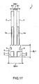
- Fig. 17 is a schematic plan view illustrating an example of a piezoelectric resonator element conventionally used in the piezoelectric devices.
- a piezoelectric resonator element 1 whose shape shown in the figure is formed by etching a piezoelectric material such as quartz or the like, is provided with a base 2, which is mounted to a package (not shown) or the like, and has a rectangular shape, and a pair of vibration arms 3 and 4, which is extended from the base 2 in the vertical direction in Fig. 17 .
- Long grooves 3a and 4a are formed on the main surfaces (front and back surface) of vibration arms, and necessary driving electrodes are formed.
- the vibration arms 3 and 4 are performed a flexural vibration so that their distal parts are moved closer and then apart, resulting in a signal having a given frequency being taken out.
- the piezoelectric resonator element 1 in which lead-out electrodes are formed at the positions indicated as numerals 5 and 6 on the base 2, is fixed to a base substrate such as a package or the like with adhesives 7 and 8 applied on the lead-out electrodes.
- cut parts 9 are formed to the base 2 so that the flexural vibration of the vibration arms is prevented from being hindered by remaining stress caused by the differences in the linear expansion coefficient between the material of the package or the like, and the material of the piezoelectric resonator element.
- the width W1 of each of the vibration arms 3 and 4 is approximately 100 ⁇ m
- the distance MW1 between them is approximately 100 ⁇ m
- the width BW1 of the base 2 is approximately 500 ⁇ m.
- JP-A-2002-261575 is the example of related art.
- the piezoelectric resonator element 1 which is miniaturized, has the following problem in its temperature characteristics.
- Figs. 18 and 19 are graphs illustrating the temperature characteristics of the piezoelectric resonator element 1.
- Fig. 18 shows a temperature-frequency characteristic.
- Fig. 19 shows a temperature-crystal impedance (CI) value characteristic.
- the temperature-frequency characteristic shown in Fig. 18 shows no problem as the same as previous, however, the temperature-CI value characteristic shown in Fig. 19 has a problem in that it is highly unstable.
- the deterioration of the temperature-CI characteristic occurs due to the change of stress condition at the positions, which are bonded with the adhesives 7 and 8, of the base 2 in the piezoelectric resonator element 1 by temperature change.
- the similar influences can occur due to the change of stress condition at the positions, which are bonded with the adhesives 7 and 8, of the base 2 when they are affected by drop shock or the like.
- An advantage of the invention is to provide a piezoelectric resonator element and a piezoelectric oscillator that have a good temperature characteristic for miniaturization.
- the present invention provides a piezoelectric resonator element according to appended claim 1, and a piezoelectric device according to claim 9.
- Preferred features are set out in the appended dependent claims. There is described in the following a piezoelectric resonator element that is provided with a base that is formed by a piezoelectric material and has a given length, and a plurality of vibration arms which is extended from one end of the base, and further, a supporting arm that is extended from the other end apart from the one end of the base by the given length to a width direction, and is extended to the same direction of the vibration arms at an outside of the vibration arms.
- the vibration arms that perform a flexural vibration are extended from one end of the base, while the supporting arm is extended from the other end of the base having the given length.
- the vibration leakage from the vibration arms that perform the flexural vibration is seldom propagated to the supporting arm, since the vibration leakage is reached to the supporting arm apart from the base through the given length of the base. Namely, if the length of the base is extremely short, it can be considered that a situation that is difficult to be controlled occurs since a leaked component of the flexural vibration spreads over the supporting arm. However, in the structure described herein, such situation is thoroughly avoided.
- the supporting arm is extended from the other end of the base to the width direction, and extended to the same direction of the vibration arm at the outside of the vibration arm, the whole size can be made compact.
- a cut part formed by shrinking the width of the piezoelectric material in the width direction may be disposed at a position, which is closer to the vibration arm than the connecting part at which the supporting arm is integrally connected to the base, of the base.
- the vibration leakage caused by the flexural vibration of the vibration arms is suppressed from being propagated to the bonding part of the supporting arm through the base.
- CI value can be prevented from being increased.
- the length of the supporting arm may be set so that the top of the supporting arm is closer to the base than the tops of the vibration arms.
- the supporting arm which has the structure in which the top of the supporting arm is closer to the base than the tops of the vibration arms in addition to the supporting arm extending in the same direction of the vibration arms, allows the whole size to be made compact.
- the supporting arm may be provided with a low stiffness structure at a position closer to the base than the bonding position at which the supporting arm is bonded to the base substrate.
- the low stiffness structure may be a shrunk width part formed halfway of the supporting arm.
- the low stiffness structure that is the shrunk width part formed halfway of the supporting arm can easily be formed when the outer shape of the piezoelectric resonator element is formed.
- the low stiffness structure may be cut part formed halfway of the supporting arm.
- the low stiffness structure that is the cut part formed halfway of the supporting arm can easily be formed when the outer shape of the piezoelectric resonator element is formed.
- a piezoelectric device described herein in which a piezoelectric resonator element is housed in a package or a case.
- the piezoelectric device is provided with a base that is formed by a piezoelectric material and has a given length, and a plurality of vibration arms which is extended from one end of the base, and further, a supporting arm that is extended from the other end apart from the one end of the base by the given length to a width direction, and is extended to the same direction of the vibration arms at an outside of the vibration arms.
- a piezoelectric device can be realized that is small and compact, and has a good temperature characteristic.
- Fig. 1 is a schematic plan view illustrating a piezoelectric device according to a first embodiment of the invention.
- Fig. 2 is a sectional-view along line A-A of Fig. 1 .
- Fig. 3 is a graph illustrating a temperature-CI value characteristic of a piezoelectric resonator element used in the piezoelectric device in Fig. 1 .
- Fig. 4 is a graph illustrating a temperature-frequency characteristic of the piezoelectric resonator element used in the piezoelectric device in Fig. 1 .
- Fig. 5 is a schematic plan view illustrating a second embodiment of the piezoelectric resonator element in Fig. 1 .
- Fig. 6 is a schematic plan view illustrating a third embodiment of the piezoelectric resonator element in Fig. 1 .
- Fig. 7 is a schematic plan view illustrating a fourth embodiment of a piezoelectric device.
- Fig. 8 is a sectional-view along line B-B of Fig. 7 .
- Fig. 9 is a schematic enlarged plan view of the piezoelectric resonator element according to a fourth embodiment.
- Fig. 10 is a sectional-view along line C-C on the vibration arms in Fig. 7 .
- Fig. 11 is a circuit diagram illustrating an oscillation circuit using the piezoelectric resonator element in Fig. 7 .
- FIG. 12 is a flow chart illustrating one example of a method for manufacturing the piezoelectric device of the invention.
- Fig. 13 is a schematic enlarged plan view of the piezoelectric resonator element according to a fifth embodiment.
- Fig. 14 is a schematic enlarged plan view of the piezoelectric resonator element according to a sixth embodiment.
- Fig. 15 is a schematic enlarged plan view of the piezoelectric resonator element according to a seventh embodiment.
- Fig. 16 shows coordinate axes of a quartz Z plate.
- Fig. 17 is a schematic plan view of a related art piezoelectric resonator element.
- Fig. 18 is a graph illustrating a temperature-frequency characteristic of the piezoelectric resonator element used in the piezoelectric device in Fig. 17 .
- Fig. 19 is a graph illustrating a temperature-CI value characteristic of the piezoelectric resonator element used in a piezoelectric device in Fig. 17 .
- Figs. 1 and 2 show a piezoelectric device according to a first embodiment of the invention.
- Fig. 1 is a schematic plan view thereof
- Fig. 2 is a schematic sectional-view taken along A-A line of Fig. 1 .
- a piezoelectric device 30 is an example including a piezoelectric resonator.
- the piezoelectric device 30 houses a piezoelectric resonator element 32 in a package 57 serving as the base substrate.
- the package 57 is formed, for example, in a rectangular box shape as shown in Figs. 1 and 2 .
- the package 57 is formed by laminating a substrate 55 as a first substrate and a substrate 56 as a second substrate.
- a substrate 55 as a first substrate
- a substrate 56 as a second substrate.
- it is formed as follows: a ceramic green sheet made of aluminum oxide is formed as an insulation material; and the sheet is formed in a shape as shown in the figures, being fired.
- the package 57 includes the inner space S formed by removing the material inside the substrate 56 serving as the second substrate as shown in Fig. 2 .
- the inner space S is a space for housing the piezoelectric resonator element 32.
- the piezoelectric resonator element 32 is placed and bonded on electrode parts 31 formed on the substrate 55 serving as the first substrate at positions of supporting arms 61 and 62 with conductive adhesives 43. On the positions, a lead-out electrode, which will be described later, is formed.
- the electrode parts 31 are connected to a mounting terminal 41 on the backside of the package via a conductive through hole, etc.
- the package 57 is hermetically sealed by bonding a lid 40, which is made of glass and transparent, with a sealing member 58 after housing the piezoelectric resonator element 32.
- frequency can be adjusted by trimming the electrode, or the like of the piezoelectric resonator element 32 with an irradiated laser beam from an outside after sealing the lid 40.
- the piezoelectric resonator element 32 is made of quartz, for example. Other than quartz, lithium tantalate, lithium niobate or other piezoelectric materials can be used.
- the piezoelectric resonator element 32 is provided with the base 51, and a pair of vibration arms 35 and 36 as shown in Fig. 1 .
- the vibration arms 35 and 36 are divided into two from one end of the base 51 (the right end of the base 51 in Fig.1 ) and extended toward the right direction in parallel with each other.
- long grooves 33 and 34 which extend in the longitudinal direction, are preferably formed respectively.
- exciting electrodes 37 and 38 which serve as a driving electrode, are disposed in the long grooves.
- each of the vibration arms 35 and 36 is gradually widened in the width as slightly tapered, playing a role of a plummet with increased weight. As a result, the vibration arms easily perform the flexural vibration.
- the piezoelectric resonator element 32 extends to the width direction of the base 51 from the other end.
- the other end (the left end of the base 51 in Fig.1 ) is apart from one end, at which the vibration arms are formed, of the base 51 with the given distance BL2 (the length of the base).
- the piezoelectric resonator element 32 is also provided with the supporting arms 61 and 62 at the positions outside the vibration arms 35 and 36 respectively.
- the supporting arms 61 and 62 extend to the direction, in which each of the vibration arms 35 and 36 extends (the right direction in Fig. 1 ), and are in parallel with the vibration arms 35 and 36.
- Each of the outer shape of the tuning-fork-like shape of the piezoelectric resonator element 32 and the long groove disposed in each of the vibration arms can be precisely formed, for example, by wet etching a material such as a quartz wafer or the like with a hydrofluoric solution or by dry etching it.
- the exciting electrodes 37 and 38 are correspondingly formed in the long grooves 33 and 34, and the side surfaces of the vibration arms. In each of the vibration arms, the electrode formed in the long groove and the electrode formed on the side surface are paired. Each of the exciting electrodes 37 and 38 is extended to each of the supporting arms 61 and 62 as each of lead-out electrodes 37a and 38a respectively. Accordingly, in a case where the piezoelectric device 30 is mounted to a mounting substrate or the like, a driving voltage from an outside is applied to each of the lead-out electrodes 37a and 38a in supporting arms 61 and 62 via each of the electrode parts 31 from the mounting terminal 41, being applied to each of the exciting electrodes 37 and 38.
- the driving voltage applied to the exciting electrode in the long grooves 33 and 34 allows electric field efficiency inside the region, in which the long groove of each of the vibration arms is formed, to be increased at the time of being driven.
- the base 51 is provided with a concaved part, which is formed by partially shrinking the dimension in the width direction of the base 51, or cut parts 71 and 72, at its both side edges.
- the both side edges are located sufficiently apart from the end part, which is adjacent to the vibration arms, of the base 51.
- Each depth of the cut parts 71 and 72 is preferably set by shrinking the width so that each bottom nearly coincides with the outer side edge of each of the vibration arms 35 and 36 respectively adjacent to the cuts parts 71 and 72.
- a vibration leakage is suppressed from being leaked to the base 51 and being propagated to the supporting arms 61 and 62 when the vibration arms 35 and 36 perform the flexural vibration.
- CI value can be suppressed at low value.
- the other end part 53, from which the supporting arms 61 and 62 are extended, of the base 51 is located so as to keep the distance BL2 sufficiently apart from a footing part 52 of the vibration arms 35 and 36.
- the dimension of the distance BL2 preferably exceeds the arm width dimension W2 of the vibration arms 35 and 36.
- the vibration arms 35 and 36 of tuning fork type resonator element perform the flexural vibration
- the area in which the vibration leakage is propagated toward the base 51 has a relative correlation with the arm width dimension W2 of the vibration arms 35 and 36.
- the inventor focuses attention to this point, having knowledge that the position serving as the base end of the supporting arms 61 and 62 should be disposed at proper position.
- the structure can be achieved in which the vibration leakage from the vibration arms 35 and 36 is more surely suppressed from being propagated to adjacent to the supporting arms 61 and 62 by the following manner: the position of the other end part 53, which serves as the base end of the supporting arms 61 and 62, is chosen so that the distance from the footing part 52 of the vibration arms to the other end part 53 exceeds the dimension corresponding to the size of the arm width dimension W2 of the vibration arms. Therefore, in order to obtain advantageous effects of the supporting arms, which will be described later, with suppressing the CI value, it is preferable that the position of the other end part 53 is apart from the footing part 52 (i.e. one end part of the base 51) of the vibration arms 35 and 36 by the distance BL2.
- the positions at which the cut parts 71 and 72 are formed are apart from the footing part 52 of the vibration arms 35 and 36 by the distance that exceeds the size of the arm width dimension W2 of the vibration arms 35 and 36. Therefore, the cut parts 71 and 72 are formed at the positions, which include a part where the supporting arms 61 and 62 are integrally connected to the base 51, and are adjacent to the vibrating arms from the part.
- the supporting arms 61 and 62 are uninvolved in the vibration, no specific conditions are required to their arm widths SW. However, it is preferable that the width SW is larger than that of the vibration arm in order to assure a supporting structure.
- the width BW2 of the base 51 can be achieved to be 500 ⁇ m by being composed of the followings: the vibration arms having the arm width W2 of approximately 50 ⁇ m; the supporting arms 61 and 62 having the width SW of approximately 100 ⁇ m; and the distance MW2 between the vibration arms is approximately 80 ⁇ m.
- the piezoelectric resonator element 32 has the width BW2, which is nearly the same of the width of the piezoelectric resonator element 1 in Fig. 17 , and shorter length. As a result, the piezoelectric resonator element 32 can be fully housed in the package having the same size as that of the conventional one.
- the embodiment can obtain the following advantageous effects while achieving such miniaturization.
- the length of the base 51 is extremely short, it can be considered that a situation that is difficult to be controlled occurs since a leaked component of the flexural vibration spreads over the supporting arms 61 and 62. However, in the embodiment, such situation is thoroughly avoided.
- the supporting arms 61 and 62 are extended from the other end part 53 of the base 51 to the width direction, and are extended to the same direction of the vibration arms 35 and 36 at outside of the vibration arms 35 and 36, the whole size can be made compact.
- the tops of the supporting arms 61 and 62 are formed so as to be closer to the base 51 than the tops of the vibration arms 35 and 36 as shown in Fig. 1 .
- the size of the piezoelectric resonator element 32 also can be made compact.
- the conductive adhesives 7 and 8 are applied to the lead-out electrodes 5 and 6, both of which are closely located. Because of this structure, the bonding process should be carried out by applying the adhesive to extremely narrow area (of the package) so that they are not contacted each other for avoiding a short, and by paying attention, even after bonding, not to flow out the adhesive to cause the short before curing it. As a result, the process is made difficult.
- the conductive adhesives 43 are merely applied to the electrode parts 31 that are respectively located at an approximately intermediate position of the supporting arms 61 and 62, both of which are spaced apart across the width direction of the package 57. This causes seldom difficulties as above described, and also no worries of the short.
- Figs. 3 and 4 are graphs illustrating the temperature characteristics of the piezoelectric resonator element 32 of the embodiment.
- Fig. 3 shows a temperature-CI value characteristic.
- Fig. 4 shows a temperature-frequency characteristic.
- the temperature-frequency characteristic in Fig. 4 shows no problem as the same as previous.
- the temperature-CI value characteristic in Fig. 3 shows extremely well as can easily be understood by comparing with Fig. 19 .
- Figs. 5 and 6 respectively show the piezoelectric resonator element according to a second embodiment and a third embodiment of the invention. They show examples in which a low stiffness structure is employed to a part of the supporting arm.
- the parts shown in these drawings that are common to the piezoelectric resonator element 32 described in Figs. 1 and 2 are given the same reference numerals, and the overlapped description thereof will be omitted here. Below, differences will be mainly described.
- the low stiffness structure is disposed at a position between the base 51 and the conductive adhesive 43, which is applied at the bonding position.
- the low stiffness structure is a shrunk width part 77 formed halfway of each of supporting arms 61-1 and 61-2.
- the arm width is gradually shrunk toward in the vicinity of the intermediate of its longitudinal direction.
- the vicinity of the intermediate is the shrunk width part having the narrowest width. Therefore, the shrunk width parts 77 are parts having the lowest stiffness in the supporting arms. The propagated strain tends to concentrate there. As a result, this structure can propagate little vibration leakage to the positions where the conductive adhesives 43 are applied.
- the shrunk width parts 77 can easily be formed by etching when forming the outer shape of the piezoelectric resonator element 32-1.
- the low stiffness structure is cut parts 75 and 76 formed halfway of each of supporting arms 61-1 and 61-2. Since the supporting arms 61-2 and 62-2 have the same structure, only the supporting arm 61-2 will be explained.
- the cut part 75 is the cut part that is cut into the width direction from the outside of the supporting arm 61-2.
- the cut part 76 is the cut part that is cut into the width direction from the inside of the supporting arm 61-2.
- both the cut parts 75 and 76 In order to more firmly prevent the flexural vibration of the vibration arms 35 and 36 from being leaked, it is better to provide both the cut parts 75 and 76. However, only one cut part can also achieve the effect reducing the vibration leakage. Forming both the cut parts 75 and 76 lessens the stiffness of the supporting arm 61-2. However, if either one is formed, no major strength reduction occurs.
- the cut parts 75 and 76 can easily be formed by etching when forming the outer shape of the piezoelectric resonator element 32-2.
- Figs. 7 and 8 show the piezoelectric device according to a fourth embodiment of the invention.
- Fig. 7 is a schematic plan view thereof
- Fig. 8 is a schematic sectional-view taken along B-B line in Fig. 7 .
- Fig. 9 is an enlarged plan view to explain the details of the piezoelectric resonator element 32 in Fig. 7 .
- Fig. 10 is a schematic sectional-view taken along C-C line on vibration arms in Fig. 7 .
- the package 57-1 which is formed, for example, in a rectangular box shape as shown in Figs. 7 and 8 , differs from the package 57 in Fig. 1 in that it is formed by laminating the following three substrates: a substrate 54 as a first substrate, the substrate 55 as a second substrate, and the substrate 56 as a third substrate.
- a through hole 27 for degassing in manufacturing processes is disposed at the bottom of the package 57-1.
- the through hole 27 is composed of a first hole 25 formed to the substrate 54 serving as the first substrate, and a second hole 26 formed to the substrate 55 serving as the second substrate.
- the second hole 26 has an outer diameter smaller than the first hole 25, and communicates to the first hole 25.
- the through hole 27 is sealed by filling a sealing member 28 so as to make the inside of the package 57-1 in airtight condition.
- the piezoelectric resonator element 32-3 is placed and bonded on electrode parts 31-1 and 31-2 formed on the substrate 55 serving as the second substrate with conductive adhesives 43 at positions of supporting arms 61 and 62 of the piezoelectric resonator element 32-3. On the positions, a lead-out electrode, which will be described later, is formed. Therefore, the bonding strength for bonding the piezoelectric resonator element 32-3 is excellent than the piezoelectric device 30 in Fig. 1 .
- the length dimension u is required to be within 60 to 80% of the whole length a of the piezoelectric resonator element 32-3 in order to achieve a stable supporting structure.
- a low stiffness part or structure which is, for example, the cut part or shrunk width part such as the structure explained with numerals 75 and 76 in Fig. 6 , may be disposed at a part of a position between the bonding position of the supporting arm 61 and the base 51. As a result, reducing the CI value or the like can be expected.
- outside corner parts 61a and 62a of the supporting arms 61 and 62 are chamfered in an R-shaped manner, which is convexed toward outside or concaved toward inside, preventing the supporting arms 61 and 62 from being damaged due to cracking, etc.
- the bonding position to the supporting arm can be chosen, for example, regarding the supporting arm 61, to be only one part corresponding to the gravity center G of the length dimension of the piezoelectric resonator element 32-3 as explained in Fig. 7 .
- the electrode parts 31-1 and 31-2 are chosen to be two points spaced apart from the gravity center located therebetween with the same distance so as to be bonded and to further strengthen the bonding structure.
- the bonding is carried out at one point regarding one supporting arm, it is preferable for achieving a sufficient bonding strength that the length of a region for applying an adhesive is maintained so as to be 25% or more of the whole length a of the piezoelectric resonator element 32-3.
- the distance between the bonding positions is 25% or more of the whole length a of the piezoelectric resonator element 32-3.
- At least one set of the electrode parts 31-1 and 31-2 among the electrode parts 31-1 and 31-2 are connected to the mounting terminals 41 on the backside of the package via conductive through holes, etc.
- the package 57 is hermetically sealed by bonding a lid 40, which is made of glass and transparent, with a sealing member 58 after housing the piezoelectric resonator element 32-3.
- a structure may be employed in which the lid 40, which is, for example, a metal plate such as covar, not a transparent material, and bonded by a seam sealing.
- each of the exciting electrodes 37 and 38 of the piezoelectric resonator element 32-3 is connected to an alternating current power supply source with a cross wiring.
- An alternating voltage serving as a driving voltage is applied to each of the vibration arms 35 and 36 from the power supply source.
- the vibration arms 35 and 36 are excited so as to be vibrated with reversed phase each other.
- a fundamental mode i.e. fundamental wave
- the vibration arms 35 and 36 are performed a flexural vibration so that their distal parts are moved closer and then apart.
- the fundamental wave of the piezoelectric resonator element 32-3 is, for example, as follows: Q value is 12000; capacitance ratio (C0/C1) is 260; CI value is 57 k ⁇ ; and frequency is 32.768 kHz (kilo hertz, hereinafter referred to as kHz).
- the second harmonic wave is, for example, as follows: Q value is 28000; capacitance ratio (C0/C1) is 5100; CI value is 77 k ⁇ ; and frequency is 207 kHz.
- the vibration arm width is the widest at the base end part T at which each of vibration arms is extended from the base 51.
- a first shrunk width part TL which drastically reduces the width between the positions of T to U, is formed.
- the position of T is the footing part of the vibration arm 36.
- the position U is apart from the position T toward the distal part of the vibration arm 36 with a little distance.
- a second shrunk width part which gradually and continuously decreases the width from the position of U to the position of P, namely, across the distance of CL of the vibration arm.
- the position of U is the end of the first shrunk width part TL.
- the position of P is apart from the position of U further toward the distal part of the vibration arm 36.
- the vibration arm 36 has a high stiffness with the first shrunk width part TL provided at the footing part close to the base.
- the vibration arm 36 also has a stiffness continuously decreased with the second shrunk width part CL, which is formed from the point U serving as the end of the first shrunk width part to the distal part.
- the part of P is the changing point P at which the width is changed. Further, it is a constricted position of the vibration arm 36 from the shape point of view. Thus, it also can be expressed as the constricted position P.
- the arm width extends from the changing point P to the distal part with the same width, or preferably, with the width gradually and slightly enlarged as shown in the figure.
- the longer the long grooves 33 and 34 in Fig. 9 more increasing the electric field efficiency of the material forming the vibration arms 35 and 36.
- the longer the long grooves, the lower CI value of the tuning fork type resonator element, at least j/b is up to approximately 0.7, where b is the whole length of vibration arm and j is the length of the long grooves 33 and 34 from the base 51. Therefore, j/b is preferably from 0.5 to 0.7.
- the whole length b of the vibration arm 36 is, for example, approximately 1250 ⁇ m in Fig. 9 .
- CI value ratio (CI value of harmonic wave/ CI value of fundamental wave) of the piezoelectric resonator element 32-3. Namely, if the CI value of a harmonic wave is smaller than the CI value of the fundamental wave since the CI value of the harmonic wave is simultaneously suppressed by reducing the CI value of the fundamental wave, oscillation with the harmonic wave easily occurs.
- the changing point P is further provided closely to the distal part of the vibration arm. This allows the CI value ratio (CI value of harmonic wave/ CI value of fundamental wave) to be more increased while reducing the CI value.
- the stiffness of the bottom part, i.e. in the vicinity of the footing part, of the vibration arm 36 is strengthen by the first shrunk width part TL. This strengthened stiffness allows the flexural vibration of the vibration arms to be more stable. As a result, the CI value can be suppressed.
- the stiffness of the vibration arm 36 is gradually lowered from its footing part, toward the distal part, to the constricted position P serving as the changing point of the vibration width. From the constricted position P to the distal part, the stiffness of the vibration arm 36 is gradually increased because the long groove 34 is not provided, and the width of the vibration arm is gradually widened.
- node of the vibration in the second harmonic wave can be shifted to the position closer to the distal part of the vibration arm 36.
- lowering the CI value of the second harmonic wave cannot be provoked while suppressing the CI value of the fundamental wave even though the CI value is increased by increasing the electric field efficiency of the piezoelectric material with elongated long groove 34.
- the CI value ratio is almost certainly increased by preferably providing the changing point P of the arm width closer to the distal part of the vibration arm from the end part of the long groove as shown in Fig. 9 , allowing the oscillation with the harmonic wave to be prevented.
- j/b an arm width shrunk ratio M, and the CI value ratio corresponding to them are correlated, where b is the whole length of the vibration arm, j is the length of the grooves 33 and 34 from the base 51, M is the ratio of the maximum width and the minimum width of the vibration arm 35, and CI value ratio is the ratio of the CI value of the second harmonic wave and the CI value of the fundamental wave.
- the oscillation with harmonic wave was able to be prevented by the CI value ratio that became more than one (1) by increasing the arm width shrunk ratio M, which is the ratio of the maximum width and the minimum width of the vibration arm 35, so as to be more than 1.06 in a case where j/b is 61.5%.
- the piezoelectric resonator element can be provided that can control the CI value of the fundamental wave at low value, and does not deteriorate drive characteristics even though it is wholly miniaturized.
- the wafer thickness i.e. the thickness of quartz wafer forming the piezoelectric resonator element, shown in Fig. 10 as the dimension x is preferably from 70 to 130 ⁇ m.
- the whole length of the piezoelectric resonator element 32-3 shown in Fig. 9 as the dimension a is approximately from 1300 to 1600 ⁇ m. It is preferable for miniaturizing the piezoelectric device that the dimension b, which is the whole length of the vibration arm, is from 1100 to 1400 ⁇ m, while the whole width d of the piezoelectric resonator element 32-3 is from 400 to 600 ⁇ m. Accordingly, in order to miniaturizing the tuning fork part, it is required for ensuring a supporting effect that the width dimension e of the base 51 is from 200 to 400 ⁇ m, while the width f of the supporting arm is from 30 to 100 ⁇ m.
- the dimension k between the vibration arms 35 and 36 in Fig. 9 is preferably from 50 to 100 ⁇ m. If the dimension k is less than 50 ⁇ m, it is difficult to sufficiently lessen a fin shaped convex part, which is an irregular shaped part due to an anisotropic etching, in the plus X axis direction in the side of the vibration arm shown in Fig. 10 with numeral 81 when the outer shape of the piezoelectric resonator element 32-3 is formed by wet etching through the quartz wafer, which will be described later. If the dimension x is 100 ⁇ m or more, the flexural vibration of vibration arms has a risk of being unstable.
- both dimensions m1 and m2 are from 3 to 15 ⁇ m. They are the dimensions between the outer edge of the long groove 33 and the outer edge of the vibration arm in the vibration arm 35 (the same as in the vibration arm 36) in Fig. 10 .
- the electric field efficiency is improved by the dimensions m1 and m2 of 15 ⁇ m and below.
- the dimensions m1 and m2 of 3 ⁇ m or more have an advantage to reliably perform a polarization of electrode.
- the first shrunk width part TL having the width dimension m of 11 ⁇ m or more in the vibration arm 36 in Fig. 9 can be expected to show a definite effect on suppressing the CI value.
- the arm width is widened from the changing point P of the arm width to the distal part by approximately from zero (0) to 20 ⁇ m with respect to the width of the changing point P of the arm width, which is the position at which the arm width of the vibration arm 36 is the minimum. Widening the width over the width described above has a risk of deteriorating a stability of the flexural vibration, since the distal part of the vibration arm 36 is too much weighted.
- An irregular shaped part 81 is formed on one side of the outside of the vibration arm 35 (the same as in the vibration arm 36) in Fig. 10 .
- the irregular shaped part 81 has a fin shape and is protruded in the plus X-axis direction. This is formed as etching remains due to the anistropic etching of quartz when the piezoelectric resonator element is wet etched for forming its outer shape.
- the protruded amount v of the irregular shaped part 81 is reduced within 5 ⁇ m by performing the etching in the etching solution containing hydrofluoric acid and ammonium fluoride for 9 to 11 hours.
- the width dimension of the long groove which is shown as the dimension g in Fig. 9 , is approximately from 60 to 90% with respect to the arm width C of vibration arm in the region, in which the long groove is formed, of the vibration arm.
- the arm width C varies at the position along the longitudinal direction of the vibration arm since the first and second shrunk width parts are formed to the vibration arms 35 and 36.
- the width g of the long groove is approximately from 60 to 90% with respect to the maximum width of the vibration arm. If the width of the long groove is smaller than this, the electric field efficiency is lowered, resulting in the CI value being increased.
- the whole length h of the base 51 in Fig. 9 which is approximately 30% with respect to the whole length a of the piezoelectric resonator element 32-3 conventionally, can be achieved to be approximately from 15 to 25% by employing the cut part, etc., in the embodiment. As a result, the miniaturization is achieved.
- the concave part or the cut parts 71 and 72 are preferably disposed at both side edges of the base 51. Its depth (the dimension q in Fig. 9 ) can be, for example, approximately 60 ⁇ m.
- the distance (dimension p) between the side of the base 51 and the supporting arm 61 or 62 is from 30 to 100 ⁇ m in order to miniaturize the package dimension.
- Fig. 11 is a circuit diagram illustrating an example of an oscillation circuit when a piezoelectric oscillator is constructed by using the piezoelectric resonator element 32 of the embodiment.
- An oscillation circuit 91 includes an amplifying circuit 92 and a feedback circuit 93.
- the amplifying circuit 92 is constructed by including an amplifier 95 and a feedback resistor 94.
- the feedback circuit 93 is constructed by including a drain resistor 96, capacitors 97 and 98, and the piezoelectric resonator element 32.
- the feedback resistor 94 is, for example, approximately 10 M ⁇ (mega ohm).
- the amplifier 95 can employ a CMOS inverter.
- the drain resistor 96 is, for example, from 200 to 900 k ⁇ (kilo ohm).
- Each of the capacitor 97 (drain capacitance) and the capacitor 97 (gate capacitance) is from 10 to 20 pF (pico farad) .
- Fig. 13 is a schematic plan view illustrating the piezoelectric resonator element according to a fifth embodiment of the invention.
- a piezoelectric resonator element 32-4 of the fifth embodiment the structure that is common to that of the piezoelectric resonator element 32-3 of the fourth embodiment is given the same numeral. The overlapped explanation of thereof is omitted. Differences will be explained below.
- Each of the piezoelectric resonator elements 61and 62 in Fig. 13 includes bonding positions, which serve as the coating region of the conductive adhesive, indicated as the numeral 43, and cut parts 75-1 and 76, which serve as a structure lowering the stiffness and are on the way to the base 51.
- the cut parts 75-1 and 76 are the same as those of the third embodiment in Fig. 6 in the viewpoint that they are formed at the outer side edge and the inner side edge in the vicinity of the base end part of each of the supporting arms. Similar to the third embodiment, they show the effect that reliably prevents the flexural vibration of the vibration arms 35 and 36 from being leaked.
- the embodiment differs from the third embodiment in that the cut parts 75-1 and 76 are formed at the same position in the longitudinal direction of each of the vibration arms 61 and 62.
- the bonding position can be employed as one part for each of the supporting arms 61 and 62 as the same as the embodiment in Fig. 1 .
- Fig. 14 is a schematic plan view illustrating the piezoelectric resonator element according to a sixth embodiment of the invention.
- a piezoelectric resonator element 32-5 of the sixth embodiment the structure that is common to that of the piezoelectric resonator element 32-3 of the fourth embodiment is given the same numeral. The overlapped explanation of thereof is omitted. Differences will be explained below.
- Each of the piezoelectric resonator elements 61and 62 in Fig. 14 includes bonding positions, each of which serves as the coating region of the conductive adhesive, indicated as the numeral 43, and a through hole 86, which serves as a structure lowering the stiffness and is on the way to the base 51.
- the through hole 86 provided to the supporting arm demonstrates the same effect as that of the cut part in the viewpoint that it can reduce the leakage of the flexural vibration of the vibration arms 35 and 36.
- providing the through hole 86 causes the stiffness drop smaller, having an advantage in strength.
- the bonding position can be employed as one part for each of the supporting arms 61 and 62 as the same as the embodiment in Fig. 1 .
- Fig. 15 is a schematic plan view illustrating the piezoelectric resonator element according to a seventh embodiment of the invention.
- a piezoelectric resonator element 32-6 of the seventh embodiment the structure that is common to that of the piezoelectric resonator element 32-3 of the fourth embodiment is given the same numeral. The overlapped explanation of thereof is omitted. Differences will be explained below.
- Each of the piezoelectric resonator elements 61and 62 in Fig. 15 includes bonding positions, which serve as the coating region of the conductive adhesive, indicated as the numeral 43, and slimmed width parts 82 and 83, which serve as a structure lowering the stiffness and are on the way to the base 51.
- each of the supporting arms 61 and 62 has the same structure, only the supporting arm 61 will be explained. Specifically, for example, bonding positions 84 and 85, in which the width dimension become larger, are formed at the positions symmetrically apart from the gravity center G of the piezoelectric resonator element 32-6 with the same distance each other in the supporting arm 61.
- the conductive adhesive 43 is applied to each of the bonding positions 84 and 85 as shown in Fig. 15 so as to be bonded to the package.
- the slimmed width parts 82 and 83 are formed by reducing the width dimension in the region excluding the bonding positions 84 and 85 and the base end part of the supporting arm 61.
- the slimmed parts 82 and 83 demonstrate the same effect as that of the cut part in the viewpoint that they can reduce the leakage of the flexural vibration of the vibration arms 35 and 36.
- the region to which the conductive adhesives 43 are applied such as the bonding positions 84 and 85 has an advantage by giving the different shape from other regions.
- the advantage is to achieve the process using image processing, etc., in the bonding process of the piezoelectric resonator element to the package in manufacturing processes described later.
- the position of the end part, which is adjacent to the base 51, of the long grooves 33 and 34 is preferably the same as the footing part of the vibration arms 35 and 36, i.e. the position of T, or is in the range in which the first shrunk width part TL is present and slightly apart from the position T toward the distal part of the vibration arm, and, particularly, is not preferably in adjacent to the base end of the base 51 from the position of T.
- the piezoelectric resonator element 32, the package 57, and the lid 40 in the piezoelectric device 30 are individually manufactured.
- the lid 40 is prepared as the lid having a suitable size for sealing the package 57 by cutting, for example, a glass plate having a given size, for example, a sheet glass of borosilicate glass.
- the package 57 is formed, as above described, by laminating a number of substrates made of aluminum-oxide ceramic green sheets and then firing the substrates.
- each of the number of substrates is provided with a given hole inside thereof so as to form a given inner space S inside when they are laminated.
- a piezoelectric substrate is prepared. Then, a given number of piezoelectric resonator elements are simultaneously formed from one piezoelectric substrate by etching their outer shapes (outer shape etching).
- a quartz wafer having a size capable for dividing it into a several number or a many number of the piezoelectric resonator elements 32 is used from piezoelectric materials as the piezoelectric substrate.
- the piezoelectric substrate is cut from the piezoelectric material, for example, a single crystal of quartz, so that the X-axis is electrical axis, the Y-axis is mechanical axis, and the Z-axis is optical axis, which are shown in Figs. 7 or 10 , because the piezoelectric substrate forms the piezoelectric resonator element 32-3 in Fig. 9 as the processes proceed.
- the piezoelectric resonator element 32 in Fig. 1 is also manufactured in the same manner.
- a quartz Z plate is cut by being rotated within a range of zero (0) to five (5) degrees in clock wise about the Z-axis (8 in Fig. 16 ) in the orthogonal coordinate system composed of the X, Y, and Z-axes when cutting it from the single crystal of quartz. Then, the quartz Z plate is cut and polished to a given thickness.
- the piezoelectric substrate exposed as the part outside from the outer shape of the piezoelectric resonator element is subjected to the etching of the outer shape of the piezoelectric resonator element by using, for example, a hydrofluoric acid solution as an etchant with a mask such as a corrosion resistant film (not shown).
- a hydrofluoric acid solution as an etchant
- a mask such as a corrosion resistant film (not shown).
- a metal film such as gold vapor deposited on chromium as an underlayer, or the like can be used.
- the etching process varies depending on the concentration, kind, temperature, and so forth of the hydrofluoric acid solution.
- the wet etching in the outer shape etching process shows the following anisotropic etching to the mechanical axis X, electrical axis Y, and optical axis Z shown in Fig. 9 as the etching proceeds.
- the etching rate in X-Y plain of the piezoelectric resonator element 32-3 is follows: in the plus X direction, the progression of etching is fast in the plain in the direction of 120 degrees with respect to the X-axis and in the plain in the direction of minus 120 degrees with respect to the X-axis; and, in the minus X direction, the progression of etching is slow in the plain in the direction of 30 degrees with respect to the X-axis and in the plain in the direction of minus 30 degrees with respect to the X-axis.
- the progression of etching speed in the Y direction is fast in the plus 30 and minus 30 degrees.
- the progression of etching speed is slow in the plus 120 and minus 120 degrees directions with respect to the Y-axis.
- the irregular shaped part protruded as a fin shape is formed on the outer side of each of vibration arms of the piezoelectric resonator element 32-3 as indicated as the numeral 81 in Fig. 10 .
- the protruded amount v of the irregular shaped part 81 explained in Fig. 10 can be extremely lessen within 5 ⁇ m by etching for sufficient time, i.e. from 9 to 11 hours, using hydrofluoric acid and ammonium fluoride as the etchant (ST11) .
- the outer shape of the piezoelectric resonator element 32-3 including the cut parts 71 and 72 is simultaneously formed.
- many piezoelectric resonator elements 32-3, each of which is connected to the quartz wafer at the vicinity of the base 51 with a slim connecting part, are achieved as their outer shapes are completed.
- the corrosion resistant film remains at the part to which the groove is not formed so as to leave both wall parts sandwiching each long groove as shown in Fig. 10 .
- the front and back side of each of the vibration arms 35 and 36 are wet etched with the same etching condition of the outer shape etching so as to form the bottom corresponding to the long groove (ST12).
- the depth of the groove indicated by the symbol t is approximately from 30 to 45% with respect to the whole thickness x.
- the electric field efficiency cannot sufficiently be improved.
- it is 45% and above there can be a case where the flexural vibration is adversely affected or the strength is insufficient due to the insufficient stiffness.
- both or either of the outer shape etching and the groove etching can be performed by dry etching.
- a metal mask is disposed in each time on the piezoelectric resonator substrate (quartz wafer) so as to cover the outer shape of the piezoelectric resonator element 32-3, or the region corresponding to the long groove after forming the outer shape.
- the piezoelectric substrate with the mask is, for example, put into a chamber (not shown), and then an etchant gas is supplied at a given degree of vacuum in the chamber so as to produce etching plasma.
- dry etching can be performed.
- a freon gas tank and an oxygen gas tank are connected to a vacuum chamber (not shown), and further an exhausting pipe is provided to the vacuum chamber so as to vacuum the chamber at a given degree of vacuum.
- a metal serving as the electrode for example, gold is deposited on the entire surface by vapor deposition or sputtering, etc.
- the electrode for driving shown in Fig. 7 is formed by photolithography using the resist exposing the part on which the electrode is not formed (ST13).
- weighted electrodes (metal films) 21 are formed on the distal part of each of the vibration arms 35 and 36 by sputtering or vapor deposition, or the like (ST14).
- the weighted electrodes 21 are not used for driving the piezoelectric resonator element 32-3 with applying a voltage, but are utilized for a frequency adjustment will be described later.
- the rough adjustment is the frequency adjustment by a mass reducing method in which a part of the weighted electrodes 21 are partially evaporated by irradiating an energy beam such as a laser beam, etc. Subsequently, the slim connecting part connected to the wafer is broken off so as to be an individual piece forming the piezoelectric resonator element 32-3 (ST16).
- the conductive adhesive 43 is applied on each of the electrodes 31-1 and 31-2 of the package 57.
- the supporting arms 61 and 62 are placed.
- the piezoelectric resonator element 32-3 is bonded to the package 57 (ST17) .
- the conductive adhesive 43 is, for example, one that is composed of a binder utilizing synthetic resins or the like, and conductive particles such as silver or the like that are mixed into the binder, and can simultaneously achieve a mechanical connection and an electrical connection.
- the through hole 27 described in Fig. 8 is not provided. Then, for example, a laser beam is irradiated to the vibration arm 35 and/or the adjacent to the distal part of the weighted electrode 21 of the vibration arm 36 while applying a driving voltage to the piezoelectric resonator element 32-3 and monitoring a frequency so that the frequency adjustment serving as a fine tuning is performed by the mass reducing method (ST18-1).
- the lid 40 is bonded to the package 57 by seam welding or the like in vacuum (ST19-1). After required inspections, the piezoelectric device 30 is completed.
- the lid 40 is bonded to the package 57 after bonding in the step of ST17 of the piezoelectric resonator element 32-3 (ST18-2) .
- the heating process is performed in which the lid 40 is bonded to the package 57 by heating a low melting point glass or the like.
- gas is produced from the low melting point glass and the conductive adhesive and the like. Accordingly, the gas is exhausted from the through hole 27 described in Fig. 8 by heating (degassing).
- a metal ball or pellet made of gold tin, more preferably, gold germanium, or the like is disposed to a stepped part 29 in vacuum, being melt by irradiating a laser beam, etc.
- the sealing member 28 made of metal in Fig. 8 hermetically seals the through hole 27 (ST19-2).
- a laser beam is irradiated so as to transmit through the lid 40, which is transparent and made of such as glass or the like, to the vibration arm 35 and/or the adjacent to the distal part of the weighted electrode 21 of the vibration arm 36.
- the frequency adjustment serving as a fine-tuning is performed by the mass reducing method (ST20-2).
- the piezoelectric device 30 is completed.
- the invention can be applied to not only the one in which the piezoelectric resonator element is housed in a box shaped package, but also to the one in which the piezoelectric resonator element is housed in a cylindrical package, the one in which the piezoelectric resonator element functions as a gyro sensor, and further to any piezoelectric devices utilizing the piezoelectric resonator element regardless the name of the piezoelectric resonator, piezoelectric oscillator, etc.
- a pair of vibration arms is formed in the piezoelectric resonator element 32.
- the number of vibration arms is not limited to this, but can be three (3) or four (4) and above.
Landscapes
- Physics & Mathematics (AREA)
- Acoustics & Sound (AREA)
- Chemical & Material Sciences (AREA)
- Crystallography & Structural Chemistry (AREA)
- Engineering & Computer Science (AREA)
- General Physics & Mathematics (AREA)
- Radar, Positioning & Navigation (AREA)
- Remote Sensing (AREA)
- Piezo-Electric Or Mechanical Vibrators, Or Delay Or Filter Circuits (AREA)
Applications Claiming Priority (3)
| Application Number | Priority Date | Filing Date | Title |
|---|---|---|---|
| JP2004305621 | 2004-10-20 | ||
| JP2005129906A JP4301200B2 (ja) | 2004-10-20 | 2005-04-27 | 圧電振動片および圧電デバイス |
| EP20050022588 EP1650866B1 (en) | 2004-10-20 | 2005-10-17 | Piezoelectric resonator element and piezoelectric device |
Related Parent Applications (2)
| Application Number | Title | Priority Date | Filing Date |
|---|---|---|---|
| EP05022588.7 Division | 2005-10-17 | ||
| EP20050022588 Division EP1650866B1 (en) | 2004-10-20 | 2005-10-17 | Piezoelectric resonator element and piezoelectric device |
Publications (3)
| Publication Number | Publication Date |
|---|---|
| EP1845616A2 EP1845616A2 (en) | 2007-10-17 |
| EP1845616A3 EP1845616A3 (en) | 2007-11-07 |
| EP1845616B1 true EP1845616B1 (en) | 2010-11-24 |
Family
ID=35645609
Family Applications (4)
| Application Number | Title | Priority Date | Filing Date |
|---|---|---|---|
| EP20070014596 Not-in-force EP1845616B1 (en) | 2004-10-20 | 2005-10-17 | Piezoelectric resonator element and piezoelectric device |
| EP20050022588 Not-in-force EP1650866B1 (en) | 2004-10-20 | 2005-10-17 | Piezoelectric resonator element and piezoelectric device |
| EP20100171212 Not-in-force EP2276172B1 (en) | 2004-10-20 | 2005-10-17 | Piezoelectric resonator element and piezoelectric device |
| EP20100171211 Not-in-force EP2276171B1 (en) | 2004-10-20 | 2005-10-17 | Piezoelectric resonator element and piezoelectric device |
Family Applications After (3)
| Application Number | Title | Priority Date | Filing Date |
|---|---|---|---|
| EP20050022588 Not-in-force EP1650866B1 (en) | 2004-10-20 | 2005-10-17 | Piezoelectric resonator element and piezoelectric device |
| EP20100171212 Not-in-force EP2276172B1 (en) | 2004-10-20 | 2005-10-17 | Piezoelectric resonator element and piezoelectric device |
| EP20100171211 Not-in-force EP2276171B1 (en) | 2004-10-20 | 2005-10-17 | Piezoelectric resonator element and piezoelectric device |
Country Status (6)
Cited By (1)
| Publication number | Priority date | Publication date | Assignee | Title |
|---|---|---|---|---|
| WO2016054667A1 (de) | 2014-10-06 | 2016-04-14 | System 7 - Railsupport GmbH | Gleisstopfmaschine zum verdichten der schotterbettung eines gleises |
Families Citing this family (67)
| Publication number | Priority date | Publication date | Assignee | Title |
|---|---|---|---|---|
| US10284143B2 (en) * | 2002-03-06 | 2019-05-07 | Piedek Technical Laboratory | Quartz crystal unit, quartz crystal oscillator and electronic apparatus |
| JP4277818B2 (ja) * | 2005-03-22 | 2009-06-10 | セイコーエプソン株式会社 | 圧電振動片および圧電デバイス |
| JP4609196B2 (ja) * | 2005-06-20 | 2011-01-12 | セイコーエプソン株式会社 | 圧電振動片および圧電デバイスならびに電子機器および携帯電話装置 |
| US7694734B2 (en) * | 2005-10-31 | 2010-04-13 | Baker Hughes Incorporated | Method and apparatus for insulating a resonator downhole |
| JP5208373B2 (ja) * | 2006-04-12 | 2013-06-12 | パナソニック株式会社 | 慣性力センサ |
| JP4414987B2 (ja) * | 2006-07-27 | 2010-02-17 | 日本電波工業株式会社 | 圧電振動子の製造方法、圧電振動子及び電子部品 |
| JP5115092B2 (ja) * | 2006-08-18 | 2013-01-09 | セイコーエプソン株式会社 | 圧電振動片、圧電デバイス、及び発振器 |
| JP5500220B2 (ja) * | 2006-08-18 | 2014-05-21 | セイコーエプソン株式会社 | 振動片、振動子、発振器、及びセンサー |
| US7579748B2 (en) | 2006-08-18 | 2009-08-25 | Epson Toyocom Corporation | Piezoelectric device and method for manufacturing thereof |
| JP2008060952A (ja) | 2006-08-31 | 2008-03-13 | Kyocera Kinseki Corp | 音叉型水晶振動板とその製造方法 |
| JP5045054B2 (ja) * | 2006-10-11 | 2012-10-10 | セイコーエプソン株式会社 | 圧電デバイス |
| JP4993080B2 (ja) * | 2007-01-22 | 2012-08-08 | セイコーエプソン株式会社 | 音叉型圧電振動片 |
| JP5045890B2 (ja) * | 2007-02-28 | 2012-10-10 | セイコーエプソン株式会社 | 圧電振動片 |
| US7863803B2 (en) * | 2007-05-30 | 2011-01-04 | Epson Toyocom Corporation | Tuning fork resonator element and tuning fork resonator |
| JP4905859B2 (ja) * | 2007-07-11 | 2012-03-28 | セイコーエプソン株式会社 | 圧電デバイスおよび圧電デバイスの製造方法 |
| ATE453954T1 (de) | 2007-07-19 | 2010-01-15 | Eta Sa Mft Horlogere Suisse | Piezoelektrischer resonator mit optimierten bewegungsfähigkeiten |
| JP5216288B2 (ja) * | 2007-09-25 | 2013-06-19 | 日本電波工業株式会社 | 圧電振動片の製造方法、圧電デバイスの製造方法 |
| JP5062413B2 (ja) * | 2007-11-08 | 2012-10-31 | セイコーエプソン株式会社 | 音叉型圧電振動片及び音叉型圧電振動子 |
| JP4629094B2 (ja) * | 2007-12-28 | 2011-02-09 | 日本電波工業株式会社 | 圧電振動片、圧電デバイス及びそれらの製造方法 |
| JP4594412B2 (ja) | 2008-05-22 | 2010-12-08 | 日本電波工業株式会社 | 圧電振動片および圧電デバイス |
| US8446079B2 (en) * | 2008-05-23 | 2013-05-21 | Statek Corporation | Piezoelectric resonator with vibration isolation |
| CN101878590B (zh) * | 2008-09-26 | 2014-07-02 | 株式会社大真空 | 音叉型压电振动片以及音叉型压电振动装置 |
| JP4709884B2 (ja) * | 2008-09-29 | 2011-06-29 | 日本電波工業株式会社 | 圧電振動片および圧電デバイス |
| JP4714770B2 (ja) * | 2008-10-06 | 2011-06-29 | 日本電波工業株式会社 | 音叉型圧電振動片及び音叉型圧電振動片の製造方法 |
| JP5155275B2 (ja) * | 2008-10-16 | 2013-03-06 | 日本電波工業株式会社 | 音叉型圧電振動片、圧電フレーム及び圧電デバイス |
| JP4709260B2 (ja) * | 2008-10-16 | 2011-06-22 | 日本電波工業株式会社 | 圧電振動片および圧電デバイス |
| JP4864962B2 (ja) * | 2008-12-17 | 2012-02-01 | 日本電波工業株式会社 | 圧電デバイス |
| JP4885206B2 (ja) | 2008-12-22 | 2012-02-29 | 日本電波工業株式会社 | 音叉型圧電振動片および圧電デバイス |
| JP2010252302A (ja) * | 2009-03-25 | 2010-11-04 | Seiko Epson Corp | 屈曲振動片およびそれを用いた発振器 |
| US8552624B2 (en) * | 2009-09-18 | 2013-10-08 | Seiko Epson Corporation | Impact resistance vibrating reed, vibrator, oscillator, and electronic device |
| JP5476964B2 (ja) * | 2009-12-09 | 2014-04-23 | セイコーエプソン株式会社 | 振動子、発振器、ジャイロ及び電子機器 |
| US8299863B2 (en) | 2009-12-25 | 2012-10-30 | Seiko Epson Corporation | Flexural mode resonator element, resonating device, and electronic apparatus |
| JP2011155629A (ja) * | 2009-12-29 | 2011-08-11 | Seiko Epson Corp | 振動片、振動子、発振器、電子機器、および周波数調整方法 |
| JP5482250B2 (ja) | 2010-02-02 | 2014-05-07 | セイコーエプソン株式会社 | 振動体および振動デバイス |
| JP5479931B2 (ja) * | 2010-02-03 | 2014-04-23 | エスアイアイ・クリスタルテクノロジー株式会社 | 圧電振動子、発振器、電子機器および電波時計 |
| US8283988B2 (en) * | 2010-02-25 | 2012-10-09 | Seiko Epson Corporation | Resonator element, resonator, oscillator, and electronic device |
| US20110227658A1 (en) * | 2010-03-16 | 2011-09-22 | Seiko Epson Corporation | Resonator element, piezoelectric device, and electronic device |
| US8304968B2 (en) * | 2010-03-17 | 2012-11-06 | Seiko Epson Corporation | Vibrator element, vibrator, oscillator, and electronic apparatus |
| US8878548B2 (en) | 2010-06-11 | 2014-11-04 | Baker Hughes Incorporated | Method for treating and sealing piezoelectric tuning forks |
| EP2400662B1 (en) * | 2010-06-18 | 2015-11-04 | Nxp B.V. | Micro-electromechanical resonator geometry |
| JP2012039226A (ja) * | 2010-08-04 | 2012-02-23 | Nippon Dempa Kogyo Co Ltd | 音叉型の圧電振動片および圧電デバイス |
| JP5552976B2 (ja) * | 2010-09-07 | 2014-07-16 | セイコーエプソン株式会社 | 角速度検出装置及び電子機器 |
| CN102055429A (zh) * | 2010-12-31 | 2011-05-11 | 苏州市东元光电科技有限公司 | 一种音叉型晶振 |
| JP5685962B2 (ja) * | 2011-02-02 | 2015-03-18 | セイコーエプソン株式会社 | 振動片、振動子、発振器及び電子機器 |
| JP5912557B2 (ja) * | 2011-03-29 | 2016-04-27 | 日本電波工業株式会社 | 音叉型圧電振動片及び圧電デバイス |
| JP5387867B2 (ja) * | 2012-04-25 | 2014-01-15 | セイコーエプソン株式会社 | 振動片 |
| TWI493866B (zh) * | 2012-05-10 | 2015-07-21 | Siward Crystal Technology Co Ltd | Piezoelectric components |
| JP2013250220A (ja) * | 2012-06-04 | 2013-12-12 | Seiko Epson Corp | 振動片、電子デバイス、及び電子機器 |
| JP6182998B2 (ja) * | 2013-06-24 | 2017-08-23 | セイコーエプソン株式会社 | 水晶振動片、振動子、電子デバイス、電子機器および移動体 |
| JP6205937B2 (ja) * | 2013-07-22 | 2017-10-04 | セイコーエプソン株式会社 | 圧電膜製造方法、振動子製造方法、振動片、振動子、発振器、電子機器及び移動体 |
| JP2015080013A (ja) * | 2013-10-15 | 2015-04-23 | セイコーエプソン株式会社 | 振動子、発振器、電子機器及び移動体 |
| JP6281254B2 (ja) * | 2013-11-16 | 2018-02-21 | セイコーエプソン株式会社 | 振動素子、振動子、発振器、電子機器および移動体 |
| JP6636683B2 (ja) * | 2014-03-07 | 2020-01-29 | エスアイアイ・クリスタルテクノロジー株式会社 | 圧電振動片及び圧電振動子 |
| JP6450551B2 (ja) * | 2014-09-30 | 2019-01-09 | エスアイアイ・クリスタルテクノロジー株式会社 | 圧電振動片及び圧電振動子 |
| JP5885825B1 (ja) * | 2014-12-25 | 2016-03-16 | エスアイアイ・クリスタルテクノロジー株式会社 | 圧電振動子および圧電振動子の製造方法 |
| JP6571339B2 (ja) * | 2015-01-26 | 2019-09-04 | エスアイアイ・クリスタルテクノロジー株式会社 | 圧電振動片及び圧電振動子 |
| JP6552225B2 (ja) * | 2015-03-12 | 2019-07-31 | エスアイアイ・クリスタルテクノロジー株式会社 | 圧電振動片及び圧電振動子 |
| JP2017060130A (ja) * | 2015-09-18 | 2017-03-23 | 京セラクリスタルデバイス株式会社 | 音叉型水晶振動素子 |
| JP6585450B2 (ja) * | 2015-09-30 | 2019-10-02 | 京セラ株式会社 | 音叉型水晶素子および水晶デバイス |
| JP6690999B2 (ja) * | 2016-05-30 | 2020-04-28 | 京セラ株式会社 | 音叉型水晶片、音叉型水晶素子、水晶デバイスおよび音叉型水晶素子の製造方法 |
| US10170684B2 (en) * | 2015-09-30 | 2019-01-01 | Kyocera Corporation | Tuning fork type crystal blank, tuning fork type crystal element, and crystal device |
| WO2017110126A1 (ja) * | 2015-12-21 | 2017-06-29 | 株式会社村田製作所 | 共振子及び共振装置 |
| US11075611B2 (en) * | 2016-10-31 | 2021-07-27 | Daishinku Corporation | Frequency adjustment method for piezoelectric resonator device |
| JP6318418B1 (ja) * | 2017-07-24 | 2018-05-09 | 有限会社ピエデック技術研究所 | 圧電振動子、圧電ユニット、圧電発振器と電子機器 |
| EP3468036A1 (fr) * | 2017-10-03 | 2019-04-10 | Micro Crystal AG | Résonateur piezo-electrique de petite taille |
| JP6675468B2 (ja) * | 2018-12-07 | 2020-04-01 | エスアイアイ・クリスタルテクノロジー株式会社 | 圧電振動片及び圧電振動子 |
| JP2022054045A (ja) * | 2020-09-25 | 2022-04-06 | セイコーエプソン株式会社 | 慣性計測装置 |
Family Cites Families (34)
| Publication number | Priority date | Publication date | Assignee | Title |
|---|---|---|---|---|
| JPS5115388A (ja) | 1974-07-29 | 1976-02-06 | Citizen Watch Co Ltd | Suishoshindoshi |
| JPS5814578B2 (ja) | 1975-05-28 | 1983-03-19 | アイシンセイキ カブシキガイシヤ | ヘンソクソウチ |
| JPS543487A (en) * | 1977-06-09 | 1979-01-11 | Citizen Watch Co Ltd | Thin-type crystal oscillator |
| JPS54113297A (en) * | 1978-01-26 | 1979-09-04 | Seiko Epson Corp | Tuning fork-type crystal vibrator |
| JPS5685922A (en) * | 1979-12-14 | 1981-07-13 | Seiko Epson Corp | Quartz oscillator |
| JPS5685921A (en) * | 1979-12-14 | 1981-07-13 | Seiko Epson Corp | Quartz oscillator |
| JPS5694813A (en) | 1979-12-27 | 1981-07-31 | Seiko Instr & Electronics Ltd | Tuning fork type piezoelectric oscillator |
| JPS57185717A (en) * | 1981-05-12 | 1982-11-16 | Citizen Watch Co Ltd | Tuning fork type quartz oscillator |
| JPS58105612A (ja) | 1981-12-17 | 1983-06-23 | Seiko Instr & Electronics Ltd | 音叉型振動子 |
| JPH01311712A (ja) | 1988-06-10 | 1989-12-15 | Seiko Electronic Components Ltd | 薄型圧電振動子ユニット |
| JPH0490613A (ja) | 1990-08-03 | 1992-03-24 | Murata Mfg Co Ltd | 圧電振動子 |
| JPH0522070A (ja) * | 1991-07-10 | 1993-01-29 | Seiko Electronic Components Ltd | 縦水晶振動子 |
| DE69628981T2 (de) * | 1995-04-04 | 2004-01-08 | Matsushita Electric Industrial Co., Ltd., Kadoma | Drehgeschwindigkeitssensor |
| JP3322153B2 (ja) | 1997-03-07 | 2002-09-09 | セイコーエプソン株式会社 | 音叉型水晶振動片 |
| JP3336921B2 (ja) * | 1997-08-04 | 2002-10-21 | 株式会社村田製作所 | 圧電共振部品 |
| US6530929B1 (en) * | 1999-10-20 | 2003-03-11 | Sdgi Holdings, Inc. | Instruments for stabilization of bony structures |
| JP2002261575A (ja) * | 2000-12-25 | 2002-09-13 | Seiko Epson Corp | 振動片、振動子、発振器及び電子機器 |
| EP1788702A3 (en) * | 2000-12-25 | 2008-01-16 | Seiko Epson Corporation | Vibrating piece, vibrator, oscillator, and electronic equipment |
| US6894428B2 (en) * | 2001-01-15 | 2005-05-17 | Seiko Epson Corporation | Vibrating piece, vibrator, oscillator, and electronic device |
| KR100398364B1 (ko) * | 2001-05-24 | 2003-09-19 | 삼성전기주식회사 | 수정진동자의 제조방법 및 그로부터 제조된 수정진동자 |
| JP4329286B2 (ja) | 2001-08-27 | 2009-09-09 | セイコーエプソン株式会社 | 振動片、振動子、発振器及び電子機器 |
| JP3812724B2 (ja) * | 2001-09-13 | 2006-08-23 | セイコーエプソン株式会社 | 振動片、振動子、発振器及び電子機器 |
| JP4001029B2 (ja) * | 2002-03-25 | 2007-10-31 | セイコーエプソン株式会社 | 音叉型圧電振動片及びその製造方法、圧電デバイス |
| JP3703773B2 (ja) * | 2002-03-28 | 2005-10-05 | 株式会社ヒューモラボラトリー | 水晶振動子の製造方法 |
| JP2004215039A (ja) * | 2003-01-06 | 2004-07-29 | Seiko Epson Corp | 圧電デバイス、圧電デバイスの製造方法、位置決め用治具、携帯電話装置及び電子機器 |
| JP3873902B2 (ja) | 2003-02-21 | 2007-01-31 | セイコーエプソン株式会社 | 圧電デバイスとその製造方法ならびに圧電デバイスを利用した携帯電話装置および圧電デバイスを利用した電子機器 |
| JP2004282498A (ja) | 2003-03-17 | 2004-10-07 | Seiko Epson Corp | 圧電振動片およびこれを利用した圧電デバイス、並びにこの圧電デバイスを利用した電子機器 |
| JP3978783B2 (ja) | 2003-03-25 | 2007-09-19 | セイコーエプソン株式会社 | 圧電デバイスと圧電デバイスを利用した携帯電話装置および圧電デバイスを利用した電子機器 |
| JP4219737B2 (ja) | 2003-05-30 | 2009-02-04 | リバーエレテック株式会社 | 圧電振動子 |
| JP4026074B2 (ja) | 2003-06-30 | 2007-12-26 | 有限会社ピエデック技術研究所 | 水晶振動子と水晶ユニットと水晶発振器 |
| JP3951058B2 (ja) | 2003-08-19 | 2007-08-01 | セイコーエプソン株式会社 | 音叉型圧電振動片 |
| JP2005094724A (ja) | 2003-09-17 | 2005-04-07 | Herutsu Kk | 音叉型水晶振動子 |
| JP2005184767A (ja) * | 2003-11-27 | 2005-07-07 | Seiko Epson Corp | 音叉型圧電振動片および音叉型圧電振動子の製造方法 |
| EP1641118B1 (en) * | 2004-09-24 | 2010-04-21 | Seiko Epson Corporation | Piezoelectric resonator element and piezoelectric device |
-
2005
- 2005-04-27 JP JP2005129906A patent/JP4301200B2/ja not_active Expired - Fee Related
- 2005-10-17 EP EP20070014596 patent/EP1845616B1/en not_active Not-in-force
- 2005-10-17 DE DE200560023823 patent/DE602005023823D1/de active Active
- 2005-10-17 EP EP20050022588 patent/EP1650866B1/en not_active Not-in-force
- 2005-10-17 EP EP20100171212 patent/EP2276172B1/en not_active Not-in-force
- 2005-10-17 EP EP20100171211 patent/EP2276171B1/en not_active Not-in-force
- 2005-10-17 US US11/252,317 patent/US7521846B2/en active Active
- 2005-10-17 DE DE200560025022 patent/DE602005025022D1/de active Active
- 2005-10-20 KR KR20050099089A patent/KR100802865B1/ko not_active Expired - Fee Related
- 2005-10-20 CN CN201010004779.6A patent/CN101820263B/zh not_active Expired - Fee Related
- 2005-10-20 CN CN200510109468A patent/CN100596020C/zh not_active Expired - Fee Related
-
2007
- 2007-01-02 KR KR1020070000297A patent/KR100786425B1/ko not_active Expired - Fee Related
- 2007-08-22 KR KR1020070084672A patent/KR101022123B1/ko not_active Expired - Fee Related
Cited By (1)
| Publication number | Priority date | Publication date | Assignee | Title |
|---|---|---|---|---|
| WO2016054667A1 (de) | 2014-10-06 | 2016-04-14 | System 7 - Railsupport GmbH | Gleisstopfmaschine zum verdichten der schotterbettung eines gleises |
Also Published As
| Publication number | Publication date |
|---|---|
| CN1764067A (zh) | 2006-04-26 |
| EP2276172A1 (en) | 2011-01-19 |
| US7521846B2 (en) | 2009-04-21 |
| EP2276172B1 (en) | 2012-08-22 |
| EP1650866A2 (en) | 2006-04-26 |
| US20060082261A1 (en) | 2006-04-20 |
| CN101820263A (zh) | 2010-09-01 |
| EP1650866A3 (en) | 2007-01-24 |
| KR100786425B1 (ko) | 2007-12-17 |
| KR101022123B1 (ko) | 2011-03-17 |
| KR20070014209A (ko) | 2007-01-31 |
| EP2276171A1 (en) | 2011-01-19 |
| DE602005025022D1 (de) | 2011-01-05 |
| CN100596020C (zh) | 2010-03-24 |
| CN101820263B (zh) | 2014-01-22 |
| EP1845616A3 (en) | 2007-11-07 |
| EP1845616A2 (en) | 2007-10-17 |
| JP2006148857A (ja) | 2006-06-08 |
| KR100802865B1 (ko) | 2008-02-12 |
| JP4301200B2 (ja) | 2009-07-22 |
| EP2276171B1 (en) | 2012-05-09 |
| KR20070096991A (ko) | 2007-10-02 |
| DE602005023823D1 (de) | 2010-11-11 |
| EP1650866B1 (en) | 2010-09-29 |
| KR20060049085A (ko) | 2006-05-18 |
Similar Documents
| Publication | Publication Date | Title |
|---|---|---|
| EP1845616B1 (en) | Piezoelectric resonator element and piezoelectric device | |
| US7863804B2 (en) | Piezoelectric vibration element and piezoelectric device | |
| KR100770826B1 (ko) | 압전 진동편 및 압전 디바이스 | |
| EP1641118B1 (en) | Piezoelectric resonator element and piezoelectric device | |
| US20080211350A1 (en) | Piezoelectric resonator element and piezoelectric device | |
| JP4609196B2 (ja) | 圧電振動片および圧電デバイスならびに電子機器および携帯電話装置 | |
| JP2008048274A (ja) | 圧電振動片および圧電デバイス | |
| JP2007096900A (ja) | 圧電振動片および圧電デバイス | |
| JP2008022413A (ja) | 圧電振動片および圧電デバイス | |
| JP4301201B2 (ja) | 圧電発振器 | |
| JP4784168B2 (ja) | 圧電振動片および圧電デバイス | |
| JP2010246126A (ja) | 圧電振動片および圧電デバイス | |
| JP5045822B2 (ja) | 圧電振動片および圧電デバイス |
Legal Events
| Date | Code | Title | Description |
|---|---|---|---|
| PUAI | Public reference made under article 153(3) epc to a published international application that has entered the european phase |
Free format text: ORIGINAL CODE: 0009012 |
|
| PUAL | Search report despatched |
Free format text: ORIGINAL CODE: 0009013 |
|
| AC | Divisional application: reference to earlier application |
Ref document number: 1650866 Country of ref document: EP Kind code of ref document: P |
|
| AK | Designated contracting states |
Kind code of ref document: A2 Designated state(s): AT BE BG CH CY CZ DE DK EE ES FI FR GB GR HU IE IS IT LI LT LU LV MC NL PL PT RO SE SI SK TR |
|
| AX | Request for extension of the european patent |
Extension state: AL BA HR MK YU |
|
| AK | Designated contracting states |
Kind code of ref document: A3 Designated state(s): AT BE BG CH CY CZ DE DK EE ES FI FR GB GR HU IE IS IT LI LT LU LV MC NL PL PT RO SE SI SK TR |
|
| AX | Request for extension of the european patent |
Extension state: AL BA HR MK YU |
|
| 17P | Request for examination filed |
Effective date: 20080507 |
|
| AKX | Designation fees paid |
Designated state(s): CH DE FR GB LI |
|
| 17Q | First examination report despatched |
Effective date: 20090804 |
|
| GRAP | Despatch of communication of intention to grant a patent |
Free format text: ORIGINAL CODE: EPIDOSNIGR1 |
|
| GRAS | Grant fee paid |
Free format text: ORIGINAL CODE: EPIDOSNIGR3 |
|
| GRAA | (expected) grant |
Free format text: ORIGINAL CODE: 0009210 |
|
| AC | Divisional application: reference to earlier application |
Ref document number: 1650866 Country of ref document: EP Kind code of ref document: P |
|
| AK | Designated contracting states |
Kind code of ref document: B1 Designated state(s): CH DE FR GB LI |
|
| REG | Reference to a national code |
Ref country code: GB Ref legal event code: FG4D |
|
| REG | Reference to a national code |
Ref country code: CH Ref legal event code: EP Ref country code: CH Ref legal event code: NV Representative=s name: BOVARD AG PATENTANWAELTE |
|
| REF | Corresponds to: |
Ref document number: 602005025022 Country of ref document: DE Date of ref document: 20110105 Kind code of ref document: P |
|
| REG | Reference to a national code |
Ref country code: CH Ref legal event code: PFA Owner name: SEIKO EPSON CORPORATION Free format text: SEIKO EPSON CORPORATION#4-1, NISHISHINJUKU 2-CHOME, SHINJUKU-KU#TOKYO 163-0811 (JP) -TRANSFER TO- SEIKO EPSON CORPORATION#4-1, NISHISHINJUKU 2-CHOME, SHINJUKU-KU#TOKYO 163-0811 (JP) |
|
| PLBE | No opposition filed within time limit |
Free format text: ORIGINAL CODE: 0009261 |
|
| STAA | Information on the status of an ep patent application or granted ep patent |
Free format text: STATUS: NO OPPOSITION FILED WITHIN TIME LIMIT |
|
| 26N | No opposition filed |
Effective date: 20110825 |
|
| REG | Reference to a national code |
Ref country code: DE Ref legal event code: R097 Ref document number: 602005025022 Country of ref document: DE Effective date: 20110825 |
|
| PGFP | Annual fee paid to national office [announced via postgrant information from national office to epo] |
Ref country code: DE Payment date: 20141014 Year of fee payment: 10 Ref country code: FR Payment date: 20141008 Year of fee payment: 10 Ref country code: GB Payment date: 20141015 Year of fee payment: 10 Ref country code: CH Payment date: 20141014 Year of fee payment: 10 |
|
| REG | Reference to a national code |
Ref country code: DE Ref legal event code: R119 Ref document number: 602005025022 Country of ref document: DE |
|
| REG | Reference to a national code |
Ref country code: CH Ref legal event code: PL |
|
| GBPC | Gb: european patent ceased through non-payment of renewal fee |
Effective date: 20151017 |
|
| PG25 | Lapsed in a contracting state [announced via postgrant information from national office to epo] |
Ref country code: DE Free format text: LAPSE BECAUSE OF NON-PAYMENT OF DUE FEES Effective date: 20160503 Ref country code: GB Free format text: LAPSE BECAUSE OF NON-PAYMENT OF DUE FEES Effective date: 20151017 Ref country code: LI Free format text: LAPSE BECAUSE OF NON-PAYMENT OF DUE FEES Effective date: 20151031 Ref country code: CH Free format text: LAPSE BECAUSE OF NON-PAYMENT OF DUE FEES Effective date: 20151031 |
|
| REG | Reference to a national code |
Ref country code: FR Ref legal event code: ST Effective date: 20160630 |
|
| PG25 | Lapsed in a contracting state [announced via postgrant information from national office to epo] |
Ref country code: FR Free format text: LAPSE BECAUSE OF NON-PAYMENT OF DUE FEES Effective date: 20151102 |