EP1840947A2 - Nichtflüchtige Halbleiterspeichervorrichtung - Google Patents
Nichtflüchtige Halbleiterspeichervorrichtung Download PDFInfo
- Publication number
- EP1840947A2 EP1840947A2 EP07005504A EP07005504A EP1840947A2 EP 1840947 A2 EP1840947 A2 EP 1840947A2 EP 07005504 A EP07005504 A EP 07005504A EP 07005504 A EP07005504 A EP 07005504A EP 1840947 A2 EP1840947 A2 EP 1840947A2
- Authority
- EP
- European Patent Office
- Prior art keywords
- layer
- floating gate
- memory device
- semiconductor memory
- nonvolatile semiconductor
- Prior art date
- Legal status (The legal status is an assumption and is not a legal conclusion. Google has not performed a legal analysis and makes no representation as to the accuracy of the status listed.)
- Withdrawn
Links
Images



















Classifications
-
- H—ELECTRICITY
- H10—SEMICONDUCTOR DEVICES; ELECTRIC SOLID-STATE DEVICES NOT OTHERWISE PROVIDED FOR
- H10B—ELECTRONIC MEMORY DEVICES
- H10B41/00—Electrically erasable-and-programmable ROM [EEPROM] devices comprising floating gates
- H10B41/40—Electrically erasable-and-programmable ROM [EEPROM] devices comprising floating gates characterised by the peripheral circuit region
-
- H—ELECTRICITY
- H10—SEMICONDUCTOR DEVICES; ELECTRIC SOLID-STATE DEVICES NOT OTHERWISE PROVIDED FOR
- H10B—ELECTRONIC MEMORY DEVICES
- H10B41/00—Electrically erasable-and-programmable ROM [EEPROM] devices comprising floating gates
- H10B41/10—Electrically erasable-and-programmable ROM [EEPROM] devices comprising floating gates characterised by the top-view layout
-
- H—ELECTRICITY
- H10—SEMICONDUCTOR DEVICES; ELECTRIC SOLID-STATE DEVICES NOT OTHERWISE PROVIDED FOR
- H10B—ELECTRONIC MEMORY DEVICES
- H10B41/00—Electrically erasable-and-programmable ROM [EEPROM] devices comprising floating gates
- H10B41/30—Electrically erasable-and-programmable ROM [EEPROM] devices comprising floating gates characterised by the memory core region
- H10B41/35—Electrically erasable-and-programmable ROM [EEPROM] devices comprising floating gates characterised by the memory core region with a cell select transistor, e.g. NAND
-
- H—ELECTRICITY
- H10—SEMICONDUCTOR DEVICES; ELECTRIC SOLID-STATE DEVICES NOT OTHERWISE PROVIDED FOR
- H10B—ELECTRONIC MEMORY DEVICES
- H10B41/00—Electrically erasable-and-programmable ROM [EEPROM] devices comprising floating gates
- H10B41/40—Electrically erasable-and-programmable ROM [EEPROM] devices comprising floating gates characterised by the peripheral circuit region
- H10B41/42—Simultaneous manufacture of periphery and memory cells
- H10B41/49—Simultaneous manufacture of periphery and memory cells comprising different types of peripheral transistor
-
- H—ELECTRICITY
- H10—SEMICONDUCTOR DEVICES; ELECTRIC SOLID-STATE DEVICES NOT OTHERWISE PROVIDED FOR
- H10D—INORGANIC ELECTRIC SEMICONDUCTOR DEVICES
- H10D30/00—Field-effect transistors [FET]
- H10D30/01—Manufacture or treatment
- H10D30/021—Manufacture or treatment of FETs having insulated gates [IGFET]
- H10D30/0411—Manufacture or treatment of FETs having insulated gates [IGFET] of FETs having floating gates
-
- H—ELECTRICITY
- H10—SEMICONDUCTOR DEVICES; ELECTRIC SOLID-STATE DEVICES NOT OTHERWISE PROVIDED FOR
- H10D—INORGANIC ELECTRIC SEMICONDUCTOR DEVICES
- H10D30/00—Field-effect transistors [FET]
- H10D30/60—Insulated-gate field-effect transistors [IGFET]
- H10D30/68—Floating-gate IGFETs
- H10D30/681—Floating-gate IGFETs having only two programming levels
- H10D30/683—Floating-gate IGFETs having only two programming levels programmed by tunnelling of carriers, e.g. Fowler-Nordheim tunnelling
-
- H—ELECTRICITY
- H10—SEMICONDUCTOR DEVICES; ELECTRIC SOLID-STATE DEVICES NOT OTHERWISE PROVIDED FOR
- H10D—INORGANIC ELECTRIC SEMICONDUCTOR DEVICES
- H10D30/00—Field-effect transistors [FET]
- H10D30/60—Insulated-gate field-effect transistors [IGFET]
- H10D30/68—Floating-gate IGFETs
- H10D30/681—Floating-gate IGFETs having only two programming levels
- H10D30/684—Floating-gate IGFETs having only two programming levels programmed by hot carrier injection
- H10D30/685—Floating-gate IGFETs having only two programming levels programmed by hot carrier injection from the channel
-
- H—ELECTRICITY
- H10—SEMICONDUCTOR DEVICES; ELECTRIC SOLID-STATE DEVICES NOT OTHERWISE PROVIDED FOR
- H10D—INORGANIC ELECTRIC SEMICONDUCTOR DEVICES
- H10D64/00—Electrodes of devices having potential barriers
- H10D64/01—Manufacture or treatment
- H10D64/031—Manufacture or treatment of data-storage electrodes
- H10D64/035—Manufacture or treatment of data-storage electrodes comprising conductor-insulator-conductor-insulator-semiconductor structures
-
- H—ELECTRICITY
- H10—SEMICONDUCTOR DEVICES; ELECTRIC SOLID-STATE DEVICES NOT OTHERWISE PROVIDED FOR
- H10D—INORGANIC ELECTRIC SEMICONDUCTOR DEVICES
- H10D64/00—Electrodes of devices having potential barriers
- H10D64/60—Electrodes characterised by their materials
- H10D64/66—Electrodes having a conductor capacitively coupled to a semiconductor by an insulator, e.g. MIS electrodes
- H10D64/68—Electrodes having a conductor capacitively coupled to a semiconductor by an insulator, e.g. MIS electrodes characterised by the insulator, e.g. by the gate insulator
- H10D64/681—Electrodes having a conductor capacitively coupled to a semiconductor by an insulator, e.g. MIS electrodes characterised by the insulator, e.g. by the gate insulator having a compositional variation, e.g. multilayered
- H10D64/685—Electrodes having a conductor capacitively coupled to a semiconductor by an insulator, e.g. MIS electrodes characterised by the insulator, e.g. by the gate insulator having a compositional variation, e.g. multilayered being perpendicular to the channel plane
-
- H—ELECTRICITY
- H10—SEMICONDUCTOR DEVICES; ELECTRIC SOLID-STATE DEVICES NOT OTHERWISE PROVIDED FOR
- H10D—INORGANIC ELECTRIC SEMICONDUCTOR DEVICES
- H10D86/00—Integrated devices formed in or on insulating or conducting substrates, e.g. formed in silicon-on-insulator [SOI] substrates or on stainless steel or glass substrates
- H10D86/40—Integrated devices formed in or on insulating or conducting substrates, e.g. formed in silicon-on-insulator [SOI] substrates or on stainless steel or glass substrates characterised by multiple TFTs
-
- H—ELECTRICITY
- H10—SEMICONDUCTOR DEVICES; ELECTRIC SOLID-STATE DEVICES NOT OTHERWISE PROVIDED FOR
- H10D—INORGANIC ELECTRIC SEMICONDUCTOR DEVICES
- H10D86/00—Integrated devices formed in or on insulating or conducting substrates, e.g. formed in silicon-on-insulator [SOI] substrates or on stainless steel or glass substrates
- H10D86/40—Integrated devices formed in or on insulating or conducting substrates, e.g. formed in silicon-on-insulator [SOI] substrates or on stainless steel or glass substrates characterised by multiple TFTs
- H10D86/431—Integrated devices formed in or on insulating or conducting substrates, e.g. formed in silicon-on-insulator [SOI] substrates or on stainless steel or glass substrates characterised by multiple TFTs having different compositions, shapes, layouts or thicknesses of gate insulators in different TFTs
-
- H—ELECTRICITY
- H10—SEMICONDUCTOR DEVICES; ELECTRIC SOLID-STATE DEVICES NOT OTHERWISE PROVIDED FOR
- H10D—INORGANIC ELECTRIC SEMICONDUCTOR DEVICES
- H10D86/00—Integrated devices formed in or on insulating or conducting substrates, e.g. formed in silicon-on-insulator [SOI] substrates or on stainless steel or glass substrates
- H10D86/40—Integrated devices formed in or on insulating or conducting substrates, e.g. formed in silicon-on-insulator [SOI] substrates or on stainless steel or glass substrates characterised by multiple TFTs
- H10D86/60—Integrated devices formed in or on insulating or conducting substrates, e.g. formed in silicon-on-insulator [SOI] substrates or on stainless steel or glass substrates characterised by multiple TFTs wherein the TFTs are in active matrices
-
- H—ELECTRICITY
- H10—SEMICONDUCTOR DEVICES; ELECTRIC SOLID-STATE DEVICES NOT OTHERWISE PROVIDED FOR
- H10D—INORGANIC ELECTRIC SEMICONDUCTOR DEVICES
- H10D89/00—Aspects of integrated devices not covered by groups H10D84/00 - H10D88/00
- H10D89/10—Integrated device layouts
-
- H—ELECTRICITY
- H10—SEMICONDUCTOR DEVICES; ELECTRIC SOLID-STATE DEVICES NOT OTHERWISE PROVIDED FOR
- H10P—GENERIC PROCESSES OR APPARATUS FOR THE MANUFACTURE OR TREATMENT OF DEVICES COVERED BY CLASS H10
- H10P95/00—Generic processes or apparatus for manufacture or treatments not covered by the other groups of this subclass
- H10P95/06—Planarisation of inorganic insulating materials
-
- G—PHYSICS
- G11—INFORMATION STORAGE
- G11C—STATIC STORES
- G11C16/00—Erasable programmable read-only memories
- G11C16/02—Erasable programmable read-only memories electrically programmable
- G11C16/04—Erasable programmable read-only memories electrically programmable using variable threshold transistors, e.g. FAMOS
- G11C16/0408—Erasable programmable read-only memories electrically programmable using variable threshold transistors, e.g. FAMOS comprising cells containing floating gate transistors
- G11C16/0416—Erasable programmable read-only memories electrically programmable using variable threshold transistors, e.g. FAMOS comprising cells containing floating gate transistors comprising cells containing a single floating gate transistor and no select transistor, e.g. UV EPROM
-
- G—PHYSICS
- G11—INFORMATION STORAGE
- G11C—STATIC STORES
- G11C16/00—Erasable programmable read-only memories
- G11C16/02—Erasable programmable read-only memories electrically programmable
- G11C16/04—Erasable programmable read-only memories electrically programmable using variable threshold transistors, e.g. FAMOS
- G11C16/0408—Erasable programmable read-only memories electrically programmable using variable threshold transistors, e.g. FAMOS comprising cells containing floating gate transistors
- G11C16/0433—Erasable programmable read-only memories electrically programmable using variable threshold transistors, e.g. FAMOS comprising cells containing floating gate transistors comprising cells containing a single floating gate transistor and one or more separate select transistors
-
- G—PHYSICS
- G11—INFORMATION STORAGE
- G11C—STATIC STORES
- G11C16/00—Erasable programmable read-only memories
- G11C16/02—Erasable programmable read-only memories electrically programmable
- G11C16/04—Erasable programmable read-only memories electrically programmable using variable threshold transistors, e.g. FAMOS
- G11C16/0483—Erasable programmable read-only memories electrically programmable using variable threshold transistors, e.g. FAMOS comprising cells having several storage transistors connected in series
Definitions
- the present invention relates to a nonvolatile semiconductor memory device that is electrically writable, readable, and erasable, and its manufacturing method.
- the present invention relates to a structure of a floating gate in the nonvolatile semiconductor memory device.
- Nonvolatile memories in which data can be electrically rewritten and data can be stored even after the power is turned off.
- a nonvolatile memory lie in that its structure is similar to that of a MOSFET (Metal Oxide Semiconductor Field Effect Transistor) and a region capable of accumulating charges for a long period of time is provided over a channel forming region.
- Such a charge accumulating region is also referred to as a floating gate since it is formed over an insulating layer and is insulated and isolated from its surroundings. Since the floating gate is surrounded by an insulator and is electrically insulated from the surroundings, there is a feature that the floating gate retains charges that are injected thereto.
- a gate electrode called a control gate is further provided over the floating gate with an insulating layer interposed therebetween. The control gate is distinguished from the floating gate by application of predetermined voltage to the control gate in data writing or reading.
- a so-called floating gate type nonvolatile memory having such a structure, data is stored through electrical control of charge injection to and discharge from the floating gate. Specifically, charges are injected to and discharged from the floating gate by application of high voltage between a semiconductor layer in which a channel forming region is formed and a control gate. It is said that Fowler-Nordheim (F-N) type tunnel current (NAND type) or hot electrons (NOR type) flow at this time through an insulating layer over the channel forming region at this time. Accordingly, the insulating layer is also referred to as a tunnel insulating layer.
- F-N Fowler-Nordheim
- NAND type NAND type
- NOR type hot electrons
- the floating gate type nonvolatile memory is required to have a property, for securing reliability, that charges accumulated in the floating gate can be retained for 10 years or more. Accordingly, the tunnel insulating layer is required to have a thickness that allows a tunnel current to flow and to have a high insulating property so that charges do not leak.
- the floating gate formed over the tunnel insulating layer is formed using silicon that is the same semiconductor material as that of the semiconductor layer in which the channel forming region is formed.
- a method for forming the floating gate using polycrystalline silicon has been widely used, and for example, a polysilicon film deposited with a thickness of 400 nm is known (refer to Patent Document 1: Japanese Published Patent Application No. 2000-58685 , p7, FIG 7)
- a floating gate of a nonvolatile memory is formed of polycrystalline semiconductor, the energy level at a conduction band bottom thereof is equal to that of a semiconductor layer (channel forming region) formed of the same silicon material. If the thickness of polycrystalline silicon of the floating gate is reduced, the energy level at the conduction band bottom becomes higher than that of the semiconductor layer. With such a difference in energy level, fewer electrons are injected from the semiconductor layer to the floating gate and writing voltage becomes high.
- a gate insulating layer provided between the floating gate and the semiconductor layer is required to have small thickness in order to inject charges to the floating gate with low voltage.
- the gate insulating layer is required to have large thickness to prevent charge leakage and impurity entry.
- a conventional nonvolatile memory requires high write voltage and secures reliability by taking countermeasures such as error detection and error correction by providing a redundant memory cell or devising a controller, for deterioration of charge retention characteristics due to repetitive rewriting.
- One aspect of the present invention is a nonvolatile semiconductor memory device including a semiconductor layer having a channel forming region between a pair of impurity regions which are formed apart from each other; and a first insulating layer over the channel forming region; a floating gate over the channel forming region with the first insulating layer interposed therebetween; a second insulating layer over the floating gate; and a control gate over the floating gate with the second insulating layer interposed therebetween.
- the floating gate includes at least a first layer formed of a semiconductor material and a second layer formed of a metal material, or an alloy material or a metal compound material thereof.
- the floating gate of the nonvolatile semiconductor memory device includes a semiconductor layer, and a metal layer, an alloy layer, or a metal compound layer with a barrier property which is provided on a second insulating layer side of the semiconductor layer for preventing corrosion of the semiconductor layer.
- the semiconductor material forming the floating gate can be selected to meet the following requirements in relation to the semiconductor layer forming the channel forming region.
- the semiconductor material forming the floating gate can be selected to satisfy one or a plurality of the following conditions.
- a band gap of the semiconductor material forming the floating gate is preferably smaller than that of the semiconductor layer.
- a difference between the band gap of the semiconductor material forming the floating gate and the band gap of the semiconductor layer is preferably 0.1 eV or more, and the former is preferably smaller.
- a band gap of the second insulating layer provided in contact with the floating gate is preferably larger than that of the semiconductor material forming the floating gate.
- the semiconductor material preferably has lower resistivity than a material forming the semiconductor layer.
- the resistivity is preferably 40 ⁇ cm to 100 ⁇ cm.
- the semiconductor material forming the floating gate is typically and preferably germanium or a germanium compound.
- the floating gate is applied to the nonvolatile semiconductor memory device according to the present invention for charge accumulation.
- a layer of germanium oxide or germanium nitride, or an oxide layer or a nitride layer including germanium or a germanium compound can be used as long as it has a similar function (as long as it functions as a charge accumulating layer).
- the second layer constituting a part of the floating gate is preferably formed of a metal, or an alloy or a metal compound thereof.
- the metal is preferably a refractory metal such as tungsten (W), tantalum (Ta), titanium (Ti), molybdenum (Mo), chromium (Cr), or nickel (Ni).
- the alloy may be an alloy using plural kinds of the refractory metals.
- the alloy may be formed using the refractory metal and niobium, zirconium, cerium, thorium, or hafnium. Alternatively, oxide or nitride of the refractory metal may be used.
- a metal nitride such as tantalum nitride, tungsten nitride, molybdenum nitride, or titanium nitride may be used.
- a metal oxide such as tantalum oxide, titanium oxide, or molybdenum oxide may be used.
- a semiconductor layer is preferably formed over an insulating surface and isolated into an island shape. At least a semiconductor layer forming a memory element and a semiconductor layer forming a logic circuit are preferably separated from each other.
- one feature of the present invention is a nonvolatile semiconductor memory device including a semiconductor layer having a channel forming region between a pair of impurity regions which are formed apart from each other; and a first insulating layer, a floating gate, a second insulating layer, and a control gate over the semiconductor layer which roughly overlap with the channel forming region.
- This nonvolatile semiconductor memory device may include a semiconductor layer formed over an insulating surface.
- a floating gate When a floating gate is formed over a semiconductor layer with a first insulating layer functioning as a tunnel insulating layer interposed therebetween, through formation of the floating gate using a semiconductor material including at least germanium, charges can be easily injected from the semiconductor layer to the floating gate, and a charge-retention property of the floating gate can be improved.
- a layer is further formed of a metal, or an alloy or a metal compound thereof in contact with the floating gate, this layer can serve as a barrier layer for improving water resistance of the floating gate and preventing corrosion thereof. Accordingly, deterioration of the floating gate can be suppressed.
- a nonvolatile semiconductor memory device With excellent characteristics can be manufactured without reduction in productivity. Since germanium is a semiconductor and a material which belongs to Group 14 of the periodic table like silicon, microfabrication of a thin film can be performed without a burden on the manufacturing equipment.
- FIG 1 is a cross-sectional view showing a major structure of a nonvolatile semiconductor memory device according to the present invention.
- FIG 1 particularly shows a main part of a nonvolatile memory element.
- the nonvolatile memory element is manufactured using a substrate 10 having an insulating surface.
- the substrate 10 having an insulating surface can be a glass substrate, a quartz substrate, a sapphire substrate, a ceramic substrate, a metal substrate provided with an insulating layer on the surface, or the like.
- a semiconductor layer 14 is formed over the substrate 10 having an insulating surface.
- a base insulating layer 12 may be provided between the substrate 10 and the semiconductor layer 14.
- the base insulating layer 12 prevents contamination due to diffusion of an impurity such as alkali metal from the substrate 10 to the semiconductor layer 14, and may appropriately be provided as a blocking layer.
- the base insulating layer 12 is formed by a CVD method, a sputtering method, or the like using an insulating material such as silicon oxide, silicon nitride, silicon oxynitride (SiO x N y , (x > y)), or silicon nitride oxide (SiN x Oy, (x > y)).
- an insulating material such as silicon oxide, silicon nitride, silicon oxynitride (SiO x N y , (x > y)), or silicon nitride oxide (SiN x Oy, (x > y)).
- a silicon nitride oxide film may be formed as a first insulating layer
- a silicon oxynitride film may be formed as a second insulating layer.
- a silicon nitride film may be formed as the first insulating layer
- a silicon oxide film may be formed as the second insulating layer.
- the semiconductor layer 14 is preferably formed using a single crystal semiconductor or a polycrystalline semiconductor.
- the semiconductor layer 14 can be formed as follows: a semiconductor layer is formed over the entire surface of the substrate 10 by a sputtering method, a plasma CVD method, or a low-pressure CVD method, and the semiconductor layer is crystallized and then selectively etched. In other words, for the purpose of element separation, it is preferable to form an island-like semiconductor layer over an insulating surface and to form one or a plurality of nonvolatile memory elements using the island-like semiconductor layer. Silicon is preferable as a semiconductor material. Alternatively, a silicon-germanium semiconductor can also be used.
- the semiconductor layer can be crystallized employing a laser crystallization method, a crystallization method by heat treatment using rapid thermal annealing (RTA) or an annealing furnace, a crystallization method using a metal element which promotes crystallization, or a combination thereof.
- RTA rapid thermal annealing
- SOI Silicon on Insulator
- a p-type impurity may be added to the semiconductor layer 14.
- the p-type impurity may be, for example, boron and may be added at a concentration of approximately 5 ⁇ 10 15 cm -3 to 1 ⁇ 10 16 cm -3 .
- This impurity controls threshold voltage of a transistor and effectively functions when added to a channel forming region 15.
- the channel forming region 15 formed in a region which almost corresponds to a gate 26, which will be described later, is positioned between a pair of impurity regions 18 of the semiconductor layer 14.
- the pair of impurity regions 18 function as a source and a drain in the nonvolatile memory element.
- the pair of impurity regions 18 are formed by addition of phosphorus or arsenic which is an n-type impurity at a concentration of approximately 1 ⁇ 10 19 cm -3 to 1 ⁇ 10 21 cm -3 .
- a first insulating layer 16 Over the semiconductor layer 14, a first insulating layer 16, a floating gate electrode 20, a second insulating layer 22, and a control gate electrode 24 are formed.
- a stacked structure from the floating gate electrode 20 to the control gate electrode 24 may be referred to as the gate 26.
- the first insulating layer 16 can be formed using silicon oxide or a stacked structure of silicon oxide and silicon nitride.
- the first insulating layer 16 may be formed through deposition of an insulating film by a plasma CVD method or a low-pressure CVD method but is preferably formed through solid phase oxidation or solid phase nitridation by plasma treatment. This is because an insulating layer which is formed through oxidation or nitridation of the semiconductor layer (typically, a silicon layer) by plasma treatment has a dense film quality, high withstand voltage, and high reliability.
- the first insulating layer 16 is preferably durable as described above since it is used as a tunnel insulating layer for injecting charges (carriers) to the floating gate electrode 20.
- the first insulating layer 16 is preferably formed with a thickness of 1 nm to 20 nm, more preferably 3 nm to 6 nm.
- the first insulating layer 16 can be formed with a thickness of 3 nm to 6 nm.
- plasma is preferably used, which is excited by microwaves (typically, 2.45 GHz) and has an electron density of 1 ⁇ 10 11 cm -3 to 1 ⁇ 10 13 cm -3 and an electron temperature of 0.5 eV to 1.5 eV This is in order to form a dense insulating layer and to obtain a practical reaction rate in solid phase oxidation treatment or solid phase nitridation treatment at a temperature of 500 °C or less.
- microwaves typically, 2.45 GHz
- the plasma treatment is performed in an oxygen atmosphere (for example, an atmosphere containing oxygen (O 2 ) or dinitrogen monoxide (N 2 O) and a rare gas (at least one of He, Ne, Ar, Kr, and Xe), or an atmosphere containing oxygen or dinitrogen monoxide, hydrogen (H 2 ), and a rare gas).
- an oxygen atmosphere for example, an atmosphere containing oxygen (O 2 ) or dinitrogen monoxide (N 2 O) and a rare gas (at least one of He, Ne, Ar, Kr, and Xe), or an atmosphere containing oxygen or dinitrogen monoxide, hydrogen (H 2 ), and a rare gas).
- the plasma treatment is performed in a nitrogen atmosphere (for example, an atmosphere containing nitrogen (N 2 ) and a rare gas (at least one of He, Ne, Ar, Kr, and Xe), an atmosphere containing nitrogen, hydrogen, and a rare gas, or an atmosphere containing NH 3 and a rare gas).
- a nitrogen atmosphere for example, an atmosphere containing nitrogen (N 2 ) and a rare gas (at least one of He, Ne, Ar, Kr, and Xe), an atmosphere containing nitrogen, hydrogen, and a rare gas, or an atmosphere containing NH 3 and a rare gas.
- a rare gas Ar can be used, for example.
- a gas in which Ar and Kr are mixed may be used.
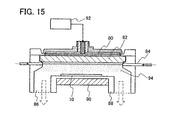
- FIG 15 shows a structural example of an apparatus for performing plasma treatment.
- This plasma treatment apparatus includes a support 88 on which the substrate 10 is arranged, a gas supplying portion 84 for introducing a gas, an exhaust port 86 connected to a vacuum pump for exhausting a gas, an antenna 80, a dielectric plate 82, and a microwave supplying portion 92 which supplies a microwave for plasma generation.
- the support 88 can be provided with a temperature controlling portion 90 to control the temperature of the substrate 10.
- the plasma treatment includes oxidation treatment, nitridation treatment, oxynitridation treatment, hydrogenation treatment, and surface modification treatment performed to a semiconductor layer, an insulating layer, and a conductive layer.
- a gas supplied from the gas supplying portion 84 may be selected in accordance with an intended purpose.
- Oxidation treatment or nitridation treatment may be performed as follows. First, a processing chamber is evacuated and a gas containing oxygen or nitrogen for plasma treatment is introduced from the gas supplying portion 84. The substrate 10 is at the room temperature or heated at a temperature of 100°C to 550°C by the temperature controlling portion 90. It is to be noted that the distance between the substrate 10 and the dielectric plate 82 is approximately 20 mm to 80 mm (preferably 20 mm to 60 mm). Next, microwaves are supplied from the microwave supplying portion 92 to the antenna 80. Then, the microwaves are introduced from the antenna 80 into the processing chamber through the dielectric plate 82; thus, plasma 94 is generated.
- plasma which has low electron temperature (3 eV or less, preferably 1.5 eV or less) and high electron density (1 ⁇ 10 11 cm -3 or more) can be generated.
- oxygen radicals containing OH radicals in some cases
- nitrogen radicals containing NH radicals in some cases
- a plasma treatment gas mixed with a rare gas such as argon enables oxygen radicals or nitrogen radicals to be generated efficiently due to excited species of a rare gas.
- a silicon oxide layer 16a is formed over the semiconductor layer 14 with a thickness of 3 nm to 6 nm by performing the plasma treatment in an oxygen atmosphere, and the surface of the silicon oxide layer 16a is treated with nitridation plasma to form a nitrogen plasma treatment layer 16b.
- the silicon oxide layer 16a is first formed over the semiconductor layer 14 by plasma treatment in oxygen atmosphere with a thickness of 3 nm to 6 nm.
- the nitrogen plasma treatment layer 16b with high nitrogen concentration is successively provided on or adjacent to the surface of the silicon oxide layer through plasma treatment in nitrogen atmosphere.
- adjacent to the surface refers to a region with a depth of approximately 0.5 nm to 1.5 nm from the surface of the silicon oxide layer.
- nitrogen is included at a rate of 20 atomic% to 50 atomic% in a region of the silicon oxide layer 16a with a depth of approximately 1 nm from the surface through plasma treatment in nitrogen atmosphere.
- the surface of a silicon layer which is a typical example of the semiconductor layer 14, is oxidized by plasma treatment to form a dense oxide film which has no distortion at the interface.
- a nitride layer is formed through nitridation of the oxide film by plasma treatment and through substitution of nitrogen for oxygen on the surface side, and thus, the layer can be denser. Due to this plasma treatment, an insulating layer which has high withstand voltage can be formed.
- an insulating layer similar to a thermal oxide film, which is formed at 950 °C to 1100 °C, can be obtained even when using a glass substrate having a temperature limit of 700 °C or less.
- a highly reliable tunnel insulating layer can be formed as the tunnel insulating layer of the nonvolatile memory element.
- the floating gate electrode 20 is formed over the first insulating layer 16.
- This floating gate electrode 20 includes a first floating gate electrode layer 20a and a second floating gate electrode layer 20b.
- the floating gate electrode is not limited to the two-layer structure, and a plurality of layers may be stacked.
- the first floating gate electrode layer 20a which is formed in contact with the first insulating layer 16 is preferably formed using a semiconductor material, and a material which satisfies one or a plurality of the following conditions can be selected.
- a band gap of a semiconductor material forming the first floating gate electrode layer 20a be smaller than that of the semiconductor layer 14.
- a band gap of a semiconductor material forming the first floating gate electrode layer 20a and a band gap of the semiconductor layer 14 have a difference of 0.1 eV or more, and the former be smaller. This is because when an energy level at the conduction band bottom of the floating gate electrode 20 is lower than that of the semiconductor layer 14, injectability of carriers (electrons) and a charge-retention property can be improved.
- the semiconductor material forming the first floating gate electrode layer 20a preferably has lower resistivity than a material forming the semiconductor layer 14.
- first floating gate electrode layer 20a is formed of a semiconductor material with low resistivity, voltage applied between the control gate electrode and the semiconductor layer can be prevented from being divided by the floating gate electrode, and electric field can be made to effectively act on the semiconductor layer.
- germanium is preferable because it has a specific resistance of 40 ⁇ cm to 70 ⁇ cm.
- An n-type impurity may be added to the first floating gate electrode layer 20a in order to lower resistivity. Writing characteristics can be improved when the first floating gate electrode layer 20a is thus formed using a material having a smaller band gap and a lower resistivity than that of the semiconductor layer 14.
- the semiconductor material forming the first floating gate electrode layer 20a is selected so that barrier energy for electrons of the first floating gate electrode layer 20a, which is formed by the first insulating layer 16, is higher than barrier energy for electrons in the semiconductor layer 14, which is formed by the first insulating layer 16. This is in order to facilitate carrier (electron) injection from the semiconductor layer 14 to the first floating gate electrode layer 20a and prevent charges from being discharged from the first floating gate electrode layer 20a.
- Germanium or a germanium compound can typically be selected to satisfy the above conditions.
- Silicon germanium is given as a typical example of germanium compound.
- germanium of 10 atomic% or more is contained in silicon. With the concentration of germanium of less than 10 atomic%, effect as a constituent element is weakened, and a band gap does not become smaller effectively.
- first floating gate electrode layer 20a can also be employed to form the first floating gate electrode layer 20a as long as they have similar effects.
- a ternary semiconductor material containing germanium can be used.
- the semiconductor material may be hydrogenated.
- a floating gate electrode functioning as a charge-accumulating layer of the nonvolatile memory element a layer of oxide or nitride of germanium or a germanium compound, or an oxide layer or a nitride layer containing germanium or a germanium compound can be used.
- the second floating gate electrode layer 20b provided on the second insulating layer 22 side in contact with the first floating gate electrode layer 20a is preferably formed of a metal, or an alloy or a metal compound thereof.
- the metal is preferably a refractory metal such as tungsten (W), tantalum (Ta), titanium (Ti), molybdenum (Mo), chromium (Cr), or nickel (Ni).
- An alloy using plural kinds of the refractory metals may be used.
- the alloy may be formed using the refractory metal and niobium, zirconium, cerium, thorium, or hafnium. Alternatively, oxide or nitride of the refractory metal may be used.
- Metal nitride such as tantalum nitride, tungsten nitride, molybdenum nitride, or titanium nitride may be used.
- Metal oxide such as tantalum oxide, titanium oxide, or molybdenum oxide may be used.
- the first floating gate electrode layer 20a can be stabilized.
- the second floating gate electrode layer 20b when the second floating gate electrode layer 20b is provided on the upper layer side of the first floating gate electrode layer 20a formed using germanium or a germanium compound, the second floating gate electrode layer 20b can be used as a barrier layer against water and chemicals in the manufacturing process. Therefore, the substrate can be easily handled in a photolithography step, an etching step, or a cleaning step, whereby productivity can be improved. In other words, the floating gate can be easily processed.
- the second insulating layer 22 is formed by a low-pressure CVD method, a plasma CVD method, or the like using one or a plurality of layers of silicon oxide, silicon oxynitride (SiO x N y , (x > y)), silicon nitride (SiN x ), silicon nitride oxide (SiN x O y , (x > y)), aluminum oxide (Al x O y ), and the like.
- the second insulating layer 22 is formed with a thickness of 1 nm to 20 nm, preferably 5 nm to 10 nm.
- a silicon nitride layer 22a is deposited with a thickness of 3 nm
- a silicon oxide layer 22b is deposited thereover with a thickness of 5 nm, which can be used as the second insulating layer 22.
- the second insulating layer 22 may be formed by depositing silicon oxynitride (SiO x N y (x>y)) by a CVD method and then subjecting it to nitridation treatment through the plasma treatment.
- the second insulating layer 22 may be formed by depositing silicon nitride oxide (SiN x O y (x>y)) by a plasma CVD method and then subjecting it to oxidation treatment through the plasma treatment.
- silicon nitride oxide SiN x O y (x>y)
- dielectric voltage can be improved. If such an insulating layer is used as the second insulating layer 22, it is possible to prevent leakage of charges accumulated in the floating gate electrode 20 to the control gate electrode 24 side.
- the control gate electrode 24 is preferably formed using a metal such as tantalum (Ta), tungsten (W), titanium (Ti), molybdenum (Mo), chromium (Cr), or niobium (Nb), or an alloy material or a compound material containing the metal as its main component.
- a metal such as tantalum (Ta), tungsten (W), titanium (Ti), molybdenum (Mo), chromium (Cr), or niobium (Nb), or an alloy material or a compound material containing the metal as its main component.
- a metal such as tantalum (Ta), tungsten (W), titanium (Ti), molybdenum (Mo), chromium (Cr), or niobium (Nb), or an alloy material or a compound material containing the metal as its main component.
- polycrystalline silicon to which an impurity element such as phosphorus is added can be used.
- the control gate electrode 24 may be formed using a
- the metal nitride can be tungsten nitride, molybdenum nitride, or titanium nitride.
- the metal nitride layer 24a By providing the metal nitride layer 24a, adhesion of the metal layer 24b can be improved, whereby the metal layer 24b can be prevented from peeling.
- metal nitride such as tantalum nitride has a high work function, the thickness of the first insulating layer 16 can be increased due to synergistic effect with the second insulating layer 22.
- FIG 2 shows a state where the semiconductor layer 14, the first insulating layer 16, the floating gate electrode 20, the second insulating layer 22, and the control gate electrode 24 are stacked.
- FIG 2 shows the case where voltage is not applied to the control gate electrode 24, and a Fermi level Ef of the semiconductor layer 14 and a Fermi level Efm of the control gate electrode 24 are equal to each other.
- the semiconductor layer 14 and at least the first floating gate electrode layer 20a of the floating gate electrode 20, between which the first insulating layer 16 is interposed, are formed using different materials.
- a band gap Eg1 (an energy difference between a lower end Ec of the conduction band and an upper end Ev of the valence band) of the semiconductor layer 14 and a band gap Eg2 of the first floating gate electrode layer 20a are to be different from each other, and the first floating gate electrode layer 20a has a smaller band gap than that of the semiconductor layer 14.
- silicon (1.12 eV) can be used for the semiconductor layer 14
- germanium (0.72 eV) or silicon germanium (0.73 eV to 1.0 eV) can be used for the first floating gate electrode layer 20a.
- Germanium or silicon germanium may be hydrogenated. In this case, it is acceptable as long as the hydrogen content of germanium or silicon germanium is 1 atomic% to 30 atomic%.
- the first floating gate electrode layer 20a is formed of germanium containing hydrogen, recombination centers at the interface with the first insulating layer 16 can be reduced.
- the metal layer can be formed using a material with a work function lower than that of the first floating gate electrode layer 20a. This is because a barrier is not formed against carriers (electrons) that are injected to the second floating gate electrode layer 20b. This facilitates carrier (electron) injection from the semiconductor layer 14 to the second floating gate electrode layer 20b.
- the work function of germanium which can be used for the first floating gate electrode layer 20a is 5.0 eV, so that tungsten (work function: 4.55 eV), tantalum (4.25 eV), titanium (4.33 eV), molybdenum (4.6 eV), or chromium (4.5 eV) can be used.
- the first insulating layer 16 includes the silicon oxide layer 16a (approximately 8 eV) and the nitrogen plasma treatment layer 16b (approximately 5 eV) which is obtained through nitridation of the silicon oxide by plasma treatment.
- the second insulating layer 22 includes the silicon nitride layer 22a and the silicon oxide layer 22b which are stacked from the floating gate electrode 20 side.
- the semiconductor layer 14 and the first floating gate electrode layer 20a, between which the first insulating layer 16 is interposed, are formed of different materials.
- a band gap of the semiconductor layer 14 and a band gap of the first floating gate electrode layer 20a are different from each other, and the first floating gate electrode layer 20a has a smaller band gap than the semiconductor layer 14.
- silicon (1.12 eV) can be used for the semiconductor layer 14
- germanium (0.72 eV) or silicon germanium (0.73 eV to 1.1 eV) can be used for the first floating gate electrode layer 20a.
- the band gap Eg1 of silicon of the semiconductor layer 14 and the band gap Eg2 of germanium of the first floating gate electrode layer 20a satisfy Eg1 > Eg2.
- an energy difference ⁇ E is generated between energy levels at the conduction band bottoms of the semiconductor layer 14 and the floating gate electrode 20.
- this energy difference ⁇ E contributes to reduction in writing voltage since ⁇ E acts in an electron-accelerating direction when electrons are injected from the semiconductor layer 14 to the floating gate electrode 20.
- FIG. 16 shows an energy band diagram where a semiconductor layer and a floating gate electrode are formed using the same semiconductor material.
- This energy band diagram shows a state where a semiconductor layer O1, a first insulating layer 02, a floating gate electrode 03, a second insulating layer 04, and a control gate electrode 05 are sequentially stacked. Even if the semiconductor layer 01 and the floating gate electrode 03 are formed using the same silicon material, band gaps thereof are different when the floating gate electrode 03 is formed thinly.
- a band gap of the semiconductor layer 01 is denoted by Eg1
- a band gap of the floating gate electrode 03 is denoted by Eg2.
- a band gap of silicon is increased to approximately 1.4 eV from 1.12 eV which is a value of a bulk state when silicon is formed into a thin film. Accordingly, an energy difference - ⁇ E is generated between the semiconductor layer 01 and the floating gate electrode 03 in a direction which blocks electron injection. In such a situation, high voltage is necessary for electron injection from the semiconductor layer 01 to the floating gate electrode 03. In other words, in order to reduce writing voltage, it is necessary to form the floating gate electrode 03 thickly like bulk silicon, or add phosphorus or arsenic as an n-type impurity at a high concentration. This is a disadvantage of a conventional nonvolatile memory.
- hot electrons are generated by application of positive voltage to the control gate electrode 24 and high voltage to a drain. Accordingly, the hot electrons can be injected to the floating gate electrode 20.
- F-N type tunnel current positive voltage is applied to the control gate electrode 24, and electrons are injected from the semiconductor layer 14 to the floating gate electrode 20 by F-N type tunnel current.
- FIG 6A shows voltage applied when electrons are injected to the floating gate electrode 20 by F-N type tunnel current.
- High positive voltage (10 V to 20 V) is applied to the control gate electrode 24 while 0V is applied to the source region 18a and the drain region 18b.
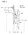
- FIG 3 shows an energy band diagram at this time.
- a high electric filed enables carriers (electrons) in the semiconductor layer 14 to be injected to the first insulating layer 16, whereby F-N type tunnel current flows.
- the band gap Eg1 of the semiconductor layer 14 and the band gap Eg2 of the floating gate electrode 20 satisfy Eg1 > Eg2. This difference acts as self-bias so that electrons injected from the channel forming region 15 of the semiconductor layer 14 are accelerated toward the floating gate electrode. Accordingly, injectability of electrons can be improved.
- An energy level at the conduction band bottom of the floating gate electrode 20 is lower than the energy level at the conduction band bottom of the semiconductor layer 14 by ⁇ E in terms of electron energy. Therefore, when electrons are injected to the floating gate electrode 20, an internal electric field generated by this energy difference acts. This phenomenon is achieved by a combination of the semiconductor layer 14 and the floating gate electrode 20 as described above. In other words, electrons can be easily injected from the semiconductor layer 14 to the floating gate electrode 20, whereby a writing property of the nonvolatile memory element can be improved. This action also applies when electrons are injected to the floating gate electrode 20 with the use of hot electrons.
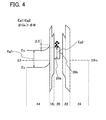
- FIG 4 shows an energy band diagram of a charge-retention state.
- Carriers in the floating gate electrode 20 are energetically trapped because they are interposed between the first insulating layer 16 and the second insulating layer 22. This means that, although potential is increased by carriers (electrons) accumulated in the floating gate electrode 20, electrons are not discharged from the floating gate electrode 20 unless energy higher than barrier energy is given to the electrons. In other words, carriers accumulated in the floating gate electrode can be retained similar to that of a reliability test in which the element is left at a constant temperature of 150 °C.
- the second floating gate electrode layer 20b can function as a floating gate which supports the first floating gate electrode layer 20a.
- electrons are not discharged from the floating gate electrode 20 unless energy higher than barrier energy is given to electrons.
- the energy level at the conduction band bottom of the floating gate electrode 20 is lower than the energy level at the conduction band bottom of the semiconductor layer 14 by ⁇ E in terms of electron energy, and the energy barrier is formed to electrons. By this barrier, electrons can be prevented from leaking to the semiconductor layer 14 by tunnel current.
- a state where data "0" is written is detected as follows: it is detected by a circuit that a transistor is not turned on when an intermediate potential Vread is applied to the control gate electrode 24.
- the intermediate potential is a potential between the threshold Voltage Vth1 in data "1” and the threshold voltage Vth2 in the data "0" (in this case, Vth1 ⁇ Vread ⁇ Vth2).
- the state where data "0" is written can be detected depending on whether the nonvolatile memory element is turned on by application of a bias voltage between the source region 18a and the drain region 18b and application of 0V to the control gate electrode 24 as shown in FIG 6B.
- FIG 7A shows a state where charges are discharged from the floating gate electrode 20 and data is erased from the nonvolatile memory element.
- negative bias voltage is applied to the control gate electrode 24, and F-N type tunnel current is applied between the semiconductor layer 14 and the floating gate electrode 20, whereby data is erased.
- negative bias voltage may be applied to the control gate electrode 24, and high positive voltage may be applied to the source region 18a, so that F-N type tunnel current is generated and electrons are extracted to the source region 18a side.
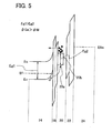
- FIG 5 shows an energy band diagram in the erasing state.
- the first insulating layer 16 can be formed thinly, electrons in the floating gate electrode 20 can be discharged to the semiconductor layer 14 side by F-N type tunnel current.
- holes can be easily injected from the channel forming region 15 of the semiconductor layer 14. Therefore, a substantial erasing operation can be achieved by injection of holes to the floating gate electrode 20.
- the thickness of the first insulating layer 16 can be small. Accordingly, electrons can be easily injected to the floating gate electrode 20 through the first insulating layer 16 by tunnel current, whereby a low-voltage operation can be performed. Further, charges can be retained at a low energy level, whereby advantageous effect in which charges may be retained stably can be obtained.
- the nonvolatile memory element according to the present invention has a structure as shown in FIGS. 2 and 3, by which self-bias is generated satisfying Eg1 > Eg2 between the semiconductor layer 14 and the floating gate electrode 20.
- This relation is highly important and enables carriers to be easily injected from the channel forming region of the semiconductor layer to the floating gate electrode. That is, writing voltage can be reduced, where as carriers can be prevented from being easily discharged from the floating gate electrode. This can improve a memory retention property of the nonvolatile memory element.
- a germanium layer as the floating gate electrode is doped with an n-type impurity, self-bias can act so that an energy level at the conduction band bottom can be further lowered, and carriers can be more easily injected to the floating gate electrode. In other words, writing voltage can be reduced, and a memory retention property of the nonvolatile memory element can be improved.
- the nonvolatile memory element As explained above, in the nonvolatile memory element according to the present invention, charges can be easily injected from the semiconductor layer to the floating gate electrode, and charges can be prevented from being discharged from the floating gate electrode. In other words, when the nonvolatile memory element operates as a memory, data can be written with very high efficiency at low voltage, and a charge-retention property can be improved.
- FIG 8 shows an example of an equivalent circuit of a nonvolatile memory cell array.
- a memory cell MS01 which stores 1-bit data includes a selection transistor S01 and a nonvolatile memory element M01.
- the selection transistor S01 is inserted in series between a bit line BL0 and the nonvolatile memory element M01, and a gate of the selection transistor S01 is connected to a word line WL1.
- a gate of the nonvolatile memory element M01 is connected to a word line WL11.
- the word line WL1 and the bit line BL0 are set at an H level, a bit line BL1 is set at a L level, and high voltage is applied to the word line WL11, whereby charges are accumulated in the floating gate electrode as described above.
- the word line WL1 and the bit line BL0 are set at an H level, and high voltage with negative polarity is applied to the word line WL11.
- the selection transistor S01 and the nonvolatile memory element M01 are formed using semiconductor layers 30 and 32, which are formed separately in island shapes over an insulating surface, respectively. Accordingly, even if an element separation region is not particularly provided, interference with other selection transistors or nonvolatile memory elements can be prevented.
- each of the selection transistor S01 and the nonvolatile memory element M01 in the memory cell MS01 is an n-channel type, so that a wiring connecting these two elements can be omitted by formation of both the elements using a single semiconductor layer which is separated in an island shape.
- FIG 9 shows a NOR type equivalent circuit in which a nonvolatile memory element is directly connected to a bit line.
- word lines WL and bit lines BL intersect, and the nonvolatile memory element is arranged at each intersection.
- a drain of each nonvolatile memory element is connected to a bit line BL.
- Sources of the nonvolatile memory elements are commonly connected to a source line SL.
- a nonvolatile memory element M01 is formed using a semiconductor layer 32, which is formed separately in an island shape over an insulating surface. Accordingly, even if an element separation region is not particularly provided, interference with other nonvolatile memory elements can be prevented. Further, a plurality of nonvolatile memory elements (such as M01 to M23 shown in FIG 9) may be regarded as one block and formed using a single semiconductor layer which is separated in an island shape. Accordingly, an erasing operation can be performed on a block basis.
- an operation of the NOR type is as follows.
- the source line SL is set at 0 V
- high voltage is applied to a word line WL which is selected for data writing
- the bit line BL is set at a potential corresponding to data "0" or "1".
- the bit line BL is set at H level and L level potentials corresponding to "0" and "1" respectively.
- Hot electrons are generated around the drain in the nonvolatile memory element to which is set at an H level potential so that data "0" is written, and the hot electrons are injected to the floating gate. In the case of data "1", such electron injection is not caused.
- the source line SL is set at 0 V and the bit line BL is set at approximately 0.8 V, and reading voltage that is set to an intermediate value of threshold voltages of data "0" and "1" is applied to the selected word line WL, and then, it is detected by a sense amplifier connected to the bit line BL depending on whether current is drawn in the nonvolatile memory element.
- FIG. 10 shows an equivalent circuit of a NAND type memory cell array.
- a NAND cell NS1 in which a plurality of nonvolatile memory elements are connected in series is connected to a bit line BL.
- a plurality of NAND cells form a block BLK.
- a block BLK1 shown in FIG 10 has 32 word lines (word lines WL0 to WL31). The nonvolatile memory elements arranged in the same row of the block BLK1 is commonly connected to a word line corresponding to this row.
- selection transistors S1 and S2 and the nonvolatile memory elements M0 to M31 are connected in series; thus, they may be formed using one semiconductor layer 34 as one group. Accordingly, a wiring connecting the nonvolatile memory elements can be omitted, whereby integration can be achieved. In addition, adjacent NAND cells can easily be separated from each other. Further, a semiconductor layer 36 of the selection transistors S1 and S2 and a semiconductor layer 38 of the NAND cell may be separately formed. In an erasing operation in which charges are extracted from each floating gate of the nonvolatile memory elements M0 to M31, the erasing operation can be performed on the NAND cell basis. Further, nonvolatile memory elements commonly connected to one word line (such as a row of M30) may be formed using one semiconductor layer 40.
- a writing operation is executed after the NAND cell NS1 is put in an erasing state, that is, a threshold voltage of each nonvolatile memory element in the NAND cell NS1 is made negative.
- Writing is sequentially performed from the nonvolatile memory element M0 closer to the source line SL. Writing to the nonvolatile memory element M0 will be outlined as an example as follows.
- Vcc power source voltage
- bit line BL0 is set at 0 V (ground voltage).
- a selection gate line SG1 is set at 0 V to turn off the selection transistor S1.
- high voltage Vpgm approximately 20 V
- intermediate voltage Vpass approximately 10 V
- the potential applied to the bit line BL0 is 0 V
- the potential of a channel forming region of the selected nonvolatile memory element M0 is 0 V
- a potential difference between the word line WL0 and the channel forming region is large, electrons are injected to the floating gate of the nonvolatile memory element M0 by F-N tunnel current as described above. Accordingly, threshold voltage of the nonvolatile memory element M0 is put in a positive state (a state where "0" is written).
- Vcc power source voltage
- high voltage with negative polarity (Vers) is applied to all the selected word lines in the selected block.
- the bit line BL and the source line SL are put in a floating state.
- electrons in the floating gate in all the memory cells in the block are discharged to the semiconductor layer by the tunnel current. Consequently, the threshold voltages of these memory cells are shifted to a negative side.
- voltage Vr (for example, 0 V) is applied to the word line WL0 of the nonvolatile memory element M0 which is selected for reading
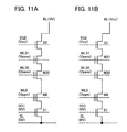
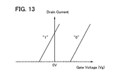
- intermediate voltage Vread for reading which is slightly higher than power source voltage is applied to the word lines WL1 to WL31 and the selection gate lines SG1 and SG2 of the memory cell which is not selected. That is, as shown in FIG 13, the memory elements other than the selected memory element each function as a transfer transistor. Accordingly, it is detected whether current flows through the nonvolatile memory element M0 which is selected for reading. In other words, when data stored in the nonvolatile memory element M0 is "0", the nonvolatile memory element M0 is off; therefore, the bit line BL does not discharge electricity. On the other hand, when data stored in the nonvolatile memory element M0 is "1", the nonvolatile memory element M0 is on; therefore, the bit line BL discharges electricity.
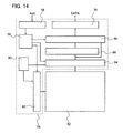
- FIG. 14 shows an example of a circuit block diagram of a nonvolatile semiconductor memory device.
- a memory cell array 52 and a peripheral circuit 54 are formed over the same substrate.
- the memory cell array 52 has a configuration as shown in FIG 8, 9, or 10.
- the peripheral circuit 54 has the following configuration.
- a row decoder 62 for selecting a word line and a column decoder 64 for selecting a bit line are provided adjacent to the memory cell array 52.
- An address is transmitted to a controlling circuit 58 through an address buffer 56, and an internal row address signal and an internal column address signal are transmitted to the row decoder 62 and the column decoder 64, respectively.
- a boosting circuit 60 which is controlled by the controlling circuit 58 in accordance with the operation mode is provided. Output of the boosting circuit 60 is supplied to a word line WL or a bit line BL through the row decoder 62 or the column decoder 64. Data output from the column decoder 64 is inputted to a sense amplifier 66. The data which is read by the sense amplifier 66 is retained in a data buffer 68, and the data is accessed randomly by the control from the controlling circuit 58 to be outputted through a data input/output buffer 70. Data to be written is temporarily retained in the data buffer 68 through the data input/output buffer 70 and transferred to the column decoder 64 by the control from the controlling circuit 58.
- the nonvolatile semiconductor memory device it is necessary to use potential that is different from the power source potential in the memory cell array 52. Therefore, it is desirable that at least the memory cell array 52 and the peripheral circuit 54 be electrically insulated and isolated.
- the nonvolatile memory element and a transistor in the peripheral circuit are each formed using a semiconductor layer formed over an insulating surface, whereby insulation and isolation can easily be achieved. Accordingly, a nonvolatile semiconductor memory device with no malfunction and less power consumption can be obtained.
- a nonvolatile memory element included in a memory portion is formed at the same time as an element such as a transistor included a logic portion, which is provided over the same substrate as the memory portion to control the memory portion or the like.
- FIG 8 shows a schematic diagram of the memory portion in the nonvolatile semiconductor memory device.
- the memory portion described in this embodiment includes a plurality of memory cells each of which has a selection transistor and a nonvolatile memory element.
- a selection transistor S01 and a nonvolatile memory element M01 form one memory cell.
- memory cells include a selection transistor S02 and a nonvolatile memory element M02, a selection transistor S03 and a nonvolatile memory element M03, a selection transistor S11 and a nonvolatile memory element M11, a selection transistor S12 and a nonvolatile memory element M12, and a selection transistor S13 and a nonvolatile memory element M13.
- a gate electrode of the selection transistor S01 is connected to a word line WL1, one of a source and a drain thereof is connected to a bit line BL0, and the other is connected to a source or a drain of the nonvolatile memory element M01. Further, a gate electrode of the nonvolatile memory element M01 is connected to a word line WL11, one of a source and a drain is connected to the source or the drain of the selection transistor S01, and the other is connected to a source line SL0.
- the selection transistor provided in the memory portion has high drive voltage compared to the transistor provided in the logic portion. Therefore, gate insulating layers or the like of the transistor provided in the memory portion and the transistor provided in the logic portion are preferably formed with different thicknesses. For example, when drive voltage is low and variation in threshold voltage is desired to be reduced, a thin film transistor in which a gate insulating film is thin is preferably provided, whereas, when drive voltage is high and a high withstand voltage of a gate insulating layer is required, a thin film transistor in which a gate insulating film is thick is preferably provided.
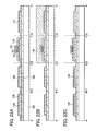
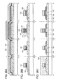
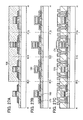
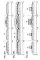
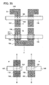
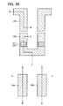
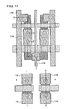
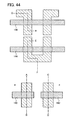
- FIGS. 32 to 34 show top views, and FIGS. 18A to 21C show cross-sectional views taken along lines A-B, C-D, E-F, and G-H of FIGS. 32 to 34.
- Portions between A and B and between C and D show thin film transistors provided in the logic portion, a portion between E and F shows a nonvolatile memory element provided in the memory portion, and a portion between G and H shows a thin film transistor provided in the memory portion.
- This embodiment will explain a case where the thin film transistor provided in the portion between A and B is a p-channel transistor, the thin film transistors provided in the portions between C and D and between G and H are n-channel transistors, and carrier movement is performed by electrons in the nonvolatile memory element provided in the portion between E and F.
- the nonvolatile semiconductor memory device of the present invention is not limited thereto.
- island-like semiconductor layers 104, 106, 108, and 110 are formed over a substrate 100 with an insulating layer 102 interposed therebetween.
- First insulating layers 112, 114, 116, and 118 are formed so as to cover the island-like semiconductor layers 104, 106, 108, and 110, respectively.
- a first conductive layer 120 and a second conductive layer 123 for forming a floating gate of the nonvolatile memory element to be completed later are stacked so as to cover the first insulating layers 112, 114, 116, and 118 (see FIG 18A).
- the island-like semiconductor layers 104, 106, 108, and 110 can be provided as follows: an amorphous semiconductor layer is formed using silicon (Si) by a sputtering method, an LPCVD method, a plasma CVD method, or the like over the insulating layer 102 which is formed over the substrate 100 in advance, and the amorphous semiconductor layer is crystallized and then selectively etched.
- the amorphous semiconductor layer can be crystallized by a laser crystallization method, a thermal crystallization method using RTA or an annealing furnace, a thermal crystallization method using a metal element which promotes crystallization, a combination thereof, or the like.
- an LD-pumped continuous wave (CW) laser (YVO 4 , the second harmonic (wavelength: 532 nm)) can be used as a laser beam source.
- the wavelength is not particularly limited to the second harmonic; however, the second harmonic is superior to other higher-order harmonics in terms of energy efficiency.
- the semiconductor layer is irradiated with a CW laser beam, the semiconductor layer continuously receives energy; therefore, once the semiconductor layer is melted, the melted state can be continuous.
- a solid-state laser is used because its output is so stable that stable treatment can be expected as compared to a gas laser or the like.
- a CW laser not only a CW laser but also a pulsed laser with a repetition rate of 10 MHz or more can be used.
- a pulsed laser with high repetition rate when the pulse interval of the laser beam is shorter than the period after the semiconductor layer is melted and before the melted semiconductor layer is solidified, the semiconductor layer can be maintained in a melted state at all times. Also, by movement of the solid-liquid interface, a semiconductor layer including crystal grains which are elongated in one direction can be formed.
- other CW lasers, or pulsed lasers with a repetition rate of 10 MHz or more can be used. Examples of gas lasers are: an Ar laser, a Kr laser, a CO 2 laser, and the like.
- solid-state lasers examples include: a YAG laser, a YLF laser, a YAlO 3 laser, a GdVO 4 laser, a KGW laser, a KYW laser, an alexandrite laser, a Ti:sapphire laser, a Y 2 O 3 laser, a YVO 4 laser, and the like.
- a YAG laser, a Y 2 O 3 laser, a GdVO 4 laser, a YVO 4 laser, or the like is also called a ceramic laser.
- metal vapor lasers are: a helium-cadmium laser, and the like.
- a laser oscillator it is preferable for a laser oscillator to emit a laser beam which is oscillated with TEM 00 (single transverse mode) because the energy homogeneity of a linear beam spot on an irradiation surface can be improved.
- TEM 00 single transverse mode
- a pulsed excimer laser may be used.
- the substrate 100 can be selected from a glass substrate, a quartz substrate, a metal substrate (such as a stainless steel substrate), a ceramic substrate, and a semiconductor substrate such as a silicon substrate.
- a plastic substrate such as a substrate of polyethylene terephthalate (PET), polyethylene naphthalate (PET), polyether sulfone (PES), acrylic, or the like can be used.
- the insulating layer 102 is formed by a CVD method, a sputtering method, or the like using an insulating material such as silicon oxide, silicon nitride, silicon oxynitride (SiO x N y , (x > y)), or silicon nitride oxide (SiN x O y , (x > y)).
- an insulating material such as silicon oxide, silicon nitride, silicon oxynitride (SiO x N y , (x > y)), or silicon nitride oxide (SiN x O y , (x > y)).
- a silicon nitride oxide film may be formed as a first insulating layer
- a silicon oxynitride film may be formed as a second insulating layer.
- a silicon nitride film may be formed as the first insulating layer, and a silicon oxide film may be formed as the second insulating layer.
- a silicon nitride film may be formed as the first insulating layer
- a silicon oxide film may be formed as the second insulating layer.
- the first insulating layers 112, 114, 116, and 118 can be formed through heat treatment, plasma treatment, or the like performed to the semiconductor layers 104, 106, 108, and 110.
- oxidation treatment, nitridation treatment, or oxynitridation treatment is performed to the semiconductor layers 104, 106, 108, and 110 by high-density plasma treatment, whereby oxide films, nitride films, or oxynitride films are formed as the first insulating layers 112, 114, 116, and 118 over the semiconductor layers 104, 106, 108, and 110, respectively.
- the first insulating layers 112, 114, 116, and 118 may be formed by a plasma CVD method or a sputtering method.
- a silicon oxide (SiO x ) film or a silicon nitride (SiN x ) film is formed as each of the first insulating layers 112, 114, 116, and 118.
- oxidation treatment may be performed to the semiconductor layers 104, 106, 108, and 110 by high-density plasma treatment, and then, nitridation treatment may be performed by performing high-density plasma treatment again.
- a silicon oxide film is formed in contact with each of the semiconductor layers 104, 106, 108, and 110 and a film containing oxygen and nitrogen (hereinafter referred to as an silicon oxynitride film) is formed over the silicon oxide film, whereby each of the first insulating layers 112, 114, 116, and 118 is a stack of the silicon oxide film and the silicon oxynitride film.
- each of the first insulating layers 112, 114, 116, and 118 is formed with a thickness of 1 nm to 10 nm, preferably 1 nm to 5 nm.
- oxidation treatment is performed to the semiconductor layers 104, 106, 108, and 110 by high-density plasma treatment, whereby a silicon oxide film with a thickness of approximately 5 nm is formed over each surface of the semiconductor layers 104, 106, 108, and 110.
- nitridation treatment is performed by high-density plasma treatment, whereby a nitrogen plasma treatment layer is formed on or adjacent to the surface of the silicon oxide film.
- silicon oxide layers are formed over the semiconductor layers 104, 106, 108, and 110 by plasma treatment in oxygen atmosphere with a thickness of 3 nm to 6 nm.
- a nitrogen plasma treatment layer with high nitrogen concentration is successively provided on or adjacent to the surface of the silicon oxide layer through plasma treatment in nitrogen atmosphere.
- nitrogen at a rate of 20 atomic% to 50 atomic% is included in a region of the silicon oxide layer with a depth of approximately 1 nm from the surface through plasma treatment in nitrogen atmosphere.
- silicon containing oxygen and nitrogen silicon oxynitride
- the oxidation treatment and the nitridation treatment by high-density plasma treatment are preferably performed successively without exposure to the air. Successively high-density plasma treatment can achieve prevention of contaminant entry and improvement in production efficiency.
- the plasma treatment is performed in an atmosphere including oxygen (for example, an atmosphere containing oxygen (O 2 ) or dinitrogen monoxide (N 2 O) and a rare gas (containing at least one of He, Ne, Ar, Kr, and Xe), or an atmosphere containing oxygen or dinitrogen monoxide, and hydrogen (H 2 ) and a rare gas).
- oxygen for example, an atmosphere containing oxygen (O 2 ) or dinitrogen monoxide (N 2 O) and a rare gas (containing at least one of He, Ne, Ar, Kr, and Xe), or an atmosphere containing oxygen or dinitrogen monoxide, and hydrogen (H 2 ) and a rare gas).
- the plasma treatment is performed in an atmosphere including nitrogen (for example, an atmosphere containing nitrogen (N 2 ) and a rare gas (containing at least one of He, Ne, Ar, Kr, and Xe), an atmosphere containing nitrogen, hydrogen, and a rare gas, or an atmosphere containing NH 3 and a rare gas).
- nitrogen for example, an atmosphere containing nitrogen (N 2 ) and a rare gas (containing at least one of He, Ne, Ar, Kr, and Xe), an atmosphere containing nitrogen, hydrogen, and a rare gas, or an atmosphere containing NH 3 and a rare gas).
- the rare gas Ar can be used, for example.
- a gas in which Ar and Kr are mixed may be used.
- the first insulating layers 112, 114, 116, and 118 may contain the rare gas (containing at least one of He, Ne, Ar, Kr, and Xe) used for the plasma treatment.
- the first insulating layers 112, 114, 116, and 118 may contain Ar.
- the high-density plasma treatment is performed in an atmosphere containing the aforementioned gas with an electron density of 1 ⁇ 10 11 cm -3 or more and a plasma electron temperature of 1.5 eV or less. Specifically, the high-density plasma treatment is performed with an electron density of 1 ⁇ 10 11 cm -3 to 1 ⁇ 10 13 cm -3 and a plasma electron temperature of 0.5 eV to 1.5 eV Since the plasma electron density is high and the electron temperature around a treatment object formed over the substrate 100 (the semiconductor layers 104, 106, 108, and 110 in this embodiment) is low, plasma damage to the treatment object can be prevented.
- the plasma electron density is as high as 1 ⁇ 10 11 cm -3 or more
- an oxide film or a nitride film formed by oxidizing or nitriding the treatment object by using the plasma treatment can be dense and superior in uniformity of its thickness and the like compared to a film formed by a CVD method, a sputtering method, or the like.
- the plasma electron temperature is as low as 1.5 eV or less
- oxidation or nitridation treatment can be performed at a lower temperature than that in the conventional plasma treatment or thermal oxidation method. For example, even plasma treatment at a temperature lower than the distortion point of a glass substrate by 100 °C or more can sufficiently perform oxidation or nitridation treatment.
- a frequency for generating plasma a high-frequency wave such as a microwave (for example, 2.45 GHz) can be used.
- a mixed gas of oxygen (O 2 ), hydrogen (H 2 ) and argon (Ar) is introduced.
- oxygen, hydrogen, and argon may be introduced at 0.1 sccm to 100 sccm, 0.1 sccm to 100 sccm, and 100 sccm to 5000 sccm, respectively.
- oxygen, hydrogen, and argon may be introduced at 5 sccm, 5 sccm, and 500 sccm, respectively.
- a mixed gas of nitrogen (N 2 ) and argon (Ar) is introduced.
- nitrogen and argon may be introduced at 20 sccm to 2000 sccm, 100 sccm to 10000 sccm, respectively.
- nitrogen and argon may be introduced at 200 sccm and 1000 sccm, respectively.
- the first insulating layer 116 formed over the semiconductor layer 108 in the memory portion functions as a tunnel oxide film in the nonvolatile memory element to be completed later. Therefore, as the first insulating layer 116 is thinner, a tunnel current flows more easily, which allows a higher-speed operation as a memory. Further, as the first insulating layer 116 is thinner, more charges can be accumulated with lower voltage in a floating gate to be formed later; therefore, power consumption of the semiconductor device can be reduced. Accordingly, the first insulating layers 112, 114, 116, and 118 are preferably formed to be thin.
- a thermal oxidation method is given as an example of a method for forming an insulating layer over a semiconductor layer.
- a substrate with a melting point which is not sufficiently high such as a glass substrate
- an insulating layer formed by a CVD method or a sputtering method has a problem in that the thickness is not sufficient because of its defects inside the film, and a defect such as a pinhole is produced when the insulating layer is formed to be thin.
- an insulating layer formed by a CVD method or a sputtering method may cover an edge of the semiconductor layer insufficiently, which may result in leakage between the semiconductor layer and a conductive film and the like to be formed over the first insulating layer 116.
- the first insulating layers 112, 114, 116, and 118 are formed by the high-density plasma treatment as described in this embodiment, the first insulating layers 112, 114, 116, and 118 can be denser than an insulating layer formed by a CVD method, a sputtering method, or the like.
- the first insulating layers 112, 114, 116, and 118 can sufficiently cover the edge portions of the semiconductor layers 104, 106, 108, and 110, respectively. As a result, an operation speed and a charge-retention property as a memory can be improved. It is to be noted that when the first insulating layers 112, 114, 116, and 118 are formed by a CVD method or a sputtering method, the surfaces of the insulating layers are preferably subjected to oxidation treatment, nitridation treatment, or oxynitridation treatment by high-density plasma treatment after the insulating layers are formed.
- the first conductive layer 120 is formed by stacking a film containing germanium, such as germanium (Ge) or a silicon germanium alloy, and a film of a metal, an alloy, or a metal compound.
- germanium such as germanium (Ge) or a silicon germanium alloy
- a film of a metal, an alloy, or a metal compound for example, the first conductive layer 120 is formed using a film containing germanium as its main component with a thickness of 1 nm to 20 nm, preferably 1 nm to 10 nm, by a plasma CVD method in an atmosphere containing a germanium element (for example, GeH 4 ).
- a germanium layer can be formed using a germane (GeH 4 ) gas diluted with hydrogen to 5 % to 10 %, by the application of a high-frequency power of 13.56 MHz to 60 MHz (for example, 27 MHz) with the substrate 100 heated at a temperature of 200 °C to 350 °C.
- a germane (GeH 4 ) gas diluted with hydrogen to 5 % to 10 %, by the application of a high-frequency power of 13.56 MHz to 60 MHz (for example, 27 MHz) with the substrate 100 heated at a temperature of 200 °C to 350 °C.
- the second conductive layer 123 is formed of a metal or an alloy thereof, or a metal compound.
- a tantalum film is formed with a thickness of 1 nm to 20 nm, preferably 1 nm to 10nm.
- the second conductive layer 123 can be formed using a refractory metal such as tungsten (W), titanium (Ti), molybdenum (Mo), chromium (Cr), or nickel (Ni).
- the alloy may be formed using the refractory metal and niobium, zirconium, cerium, thorium, or hafnium. Alternatively, oxide or nitride of the refractory metal may be used.
- the metal nitride can be tantalum nitride, tungsten nitride, molybdenum nitride, titanium nitride, or the like.
- the metal oxide can be tantalum oxide, titanium oxide, molybdenum oxide, or the like.
- the second conductive layer 123 can be formed by a sputtering method, an electron beam evaporation method, or the like. When the second conductive layer 123 is formed by a sputtering method, a target including a subject metal may be used. In forming metal oxide or metal nitride, it may be formed by reactive sputtering or with the use of a target of the metal oxide or the metal nitride. When the second conductive layer 123 to be a second floating gate electrode layer 125 later is thus formed of a metal or the like, a first floating gate electrode layer 121 formed using the first conductive layer 120 can be stabilized.
- the first insulating layers 112, 114, and 118, and the stacked structure including the first conductive layer 120 and the second conductive layer 123, which are formed over the semiconductor layers 104, 106, and 110, are removed, whereas the first insulating layer 116 and the stacked structure including the first conductive layer 120 and the second conductive layer 123, which are formed over the semiconductor layer 108, are left.
- the semiconductor layer 108, the first insulating layer 116, and the stacked structure including the first conductive layer 120 and the second conductive layer 123 provided in the memory portion are covered with a resist, and the first insulating layers 112, 114, and 118, and the stacked structure including the first conductive layer 120 and the second conductive layer 123, which are formed over the semiconductor layers 104, 106, and 110, are removed by etching (see FIG 18B).
- a resist 122 is selectively formed to cover the semiconductor layers 104, 106, and 110 and a part of the stacked structure including the first conductive layer 120 and the second conductive layer 123 formed over the semiconductor layer 108, and a part of the first conductive layer 120 and the second conductive layer 123 not covered with the resist 122 is removed by etching.
- the part of the stacked structure including the first conductive layer 120 and the second conductive layer 123 covered with the resist 122 is left; accordingly, a stacked structure including a first floating gate electrode layer 121 and a second floating gate electrode layer 125 functioning as a floating gate is formed (see FIGS. 18C and 32).
- an impurity region is formed in a specific region of the semiconductor layer 110.
- an impurity region 126 is formed by selectively forming a resist 124 to cover the semiconductor layers 104, 106, and 108 and a part of the semiconductor layer 110 after the resist 122 is removed and by introducing an impurity element to a part of the semiconductor layer 110 not covered with the resist 124 (see FIG 19A).
- an impurity element an impurity element imparting n-type conductivity or an impurity element imparting p-type conductivity is used.
- the impurity element imparting n-type conductivity phosphorus (P), arsenic (As), or the like can be used.
- the impurity element imparting p-type conductivity boron (B), aluminum (Al), gallium (Ga), or the like can be used.
- phosphorus (P) is introduced to the semiconductor layer 110.
- a second insulating layer 128 is formed to cover the semiconductor layers 104, 106, and 110, and the first insulating layer 116, and the stacked structure including and the first floating gate electrode layer 121 and the second floating gate electrode layer 125 functioning as a floating gate, which are formed over the semiconductor layer 108 (see FIG 19B).
- the second insulating layer 128 is formed by a CVD method, a sputtering method, or the like using an insulating material such as silicon oxide, silicon nitride, silicon oxynitride (SiO x N y , (x > y)), or silicon nitride oxide (SiN x O y , (x > y)) with a single layer structure or a stacked structure.
- a silicon oxynitride film or a silicon nitride oxide film is formed by a CVD method with a thickness of 5 nm to 50 nm.
- a silicon oxynitride film may be formed as a first insulating layer, a silicon nitride film may be formed as a second insulating layer, and a silicon oxynitride film may be formed as a third insulating layer.
- oxide or nitride of germanium may be used for the second insulating layer 128.
- the second insulating layer 128 formed over the semiconductor layer 108 functions as a control insulating layer in the nonvolatile memory element to be completed later, and the second insulating layer 128 formed over the semiconductor layer 110 functions as a gate insulating layer in a transistor to be completed later.
- a resist 130 is selectively formed to cover the second insulating layer 128 formed over the semiconductor layers 108 and 110, and the second insulating layer 128 formed over the semiconductor layers 104 and 106 is removed (see FIG. 19C).
- third insulating layers 132 and 134 are formed to cover the semiconductor layers 104 and 106, respectively (see FIG 20A).
- the third insulating layers 132 and 134 are formed by any of the methods described as the method for forming the first insulating layers 112, 114, 116, and 118.
- oxidation treatment, nitridation treatment, or oxynitridation treatment is performed to the semiconductor layers 104, 106, 108, and 110 by high-density plasma treatment; thus, oxide films, nitride films, or oxynitride films of silicon are formed as the third insulating layers 132 and 134 over the semiconductor layers 104 and 106, respectively.
- each of the third insulating layers 132 and 134 is formed with a thickness of 1 nm to 20 nm, preferably 1 nm to 10 nm.
- a silicon oxide film is formed on each surface of the semiconductor layers 104 and 106 by performing oxidation treatment to each of the semiconductor layers 104 and 106 by high-density plasma treatment, and then, a nitrogen plasma treatment layer is formed on or adjacent to the surface of the silicon oxide film by performing nitridation treatment by high-density plasma treatment.
- the oxidation treatment or the nitridation treatment is also performed to the surface of the second insulating layer 128 formed over the semiconductor layers 108 and 110, so that an oxide film or an oxynitride film is formed.
- Each of the third insulating layers 132 and 134 formed over the semiconductor layers 104 and 106 functions as a gate insulating layer in a transistor to be completed later.
- a conductive film is formed to cover the third insulating layers 132 and 134 formed over the semiconductor layers 104 and 106, and the second insulating layer 128 formed over the semiconductor layers 108 and 110 (see FIG 20B).
- This embodiment describes an example in which conductive films 136 and 138 are sequentially stacked as the conductive film.
- the conductive film may have a single-layer structure or a stacked structure including three or more layers.
- the conductive films 136 and 138 can be formed using an element selected from tantalum (Ta), tungsten (W), titanium (Ti), molybdenum (Mo), aluminum (Al), copper (Cu), chromium (Cr), niobium (Nb), and the like or an alloy material or a compound material containing the above element as its main component.
- a metal nitride film obtained by nitriding the above-mentioned element can be used.
- a semiconductor material typified by polycrystalline silicon doped with an impurity element such as phosphorus can be used.
- the conductive layer is provided with a stacked structure in which the conductive film 136 is formed using tantalum nitride and the conductive film 138 is formed using tungsten thereover.
- a single layer or a stacked layer of tungsten nitride, molybdenum nitride, or titanium nitride can be used as the conductive film 136, and a single layer or a stacked layer of tantalum, molybdenum, or titanium can be used as the conductive film 138.
- the stacked conductive films 136 and 138 are selectively removed by etching, so that the conductive films 136 and 138 are partially left over the semiconductor layers 104, 106, 108, and 110 to form conductive films 140, 142, 144, and 146 each functioning as a gate electrode (see FIGS. 20C and 33).
- the conductive film 144 formed over the semiconductor layer 108 provided in the memory portion functions as a control gate in the nonvolatile memory element to be completed later.
- Each of the conductive films 140, 142, and 146 functions as a gate electrode of a transistor to be completed later.
- impurity regions are formed by selectively forming a resist 148 to cover the semiconductor layer 104 and by introducing an impurity element to the semiconductor layers 106, 108, and 110 using the resist 148 and the conductive films 142, 144, and 146 as masks (see FIG. 21A).
- an impurity element imparting n-type conductivity or an impurity element imparting p-type conductivity is used.
- the impurity element imparting n-type conductivity phosphorus (P), arsenic (As), or the like can be used.
- As the impurity element imparting p-type conductivity boron (B), aluminum (Al), gallium (Ga), or the like can be used. In this embodiment, as the impurity element, phosphorus (P) is used.
- impurity regions 152 which form a source region and a drain region, and a channel forming region 150 are formed in the semiconductor layer 106.
- impurity regions 156 which form a source region and a drain region, low-concentration impurity regions 158 which form LDD regions, and a channel forming region 154 are formed.
- impurity regions 162 which form a source region and a drain region, low-concentration impurity regions 164 which form LDD regions, and a channel forming region 160 are formed.
- the low-concentration impurity regions 158 are formed in the semiconductor layer 108 by passage of the impurity element introduced in FIG 21A through the stacked structure including the first floating gate electrode layer 121 and the second floating gate electrode layer 125 functioning as a floating gate. Therefore, in the semiconductor layer 108, the channel forming region 154 is formed in a region which is overlapped by both the conductive film 144 and the stacked structure including the first floating gate electrode layer 121 and the second floating gate electrode layer 125; each of the low-concentration impurity regions 158 is formed in a region which is overlapped by the stacked structure including the first floating gate electrode layer 121 and the second floating gate electrode layer 125 and which is not overlapped by the conductive film 144; and each of the high-concentration impurity regions 156 is formed in a region which is overlapped by neither the conductive film 144 nor the stacked structure including the first floating gate electrode layer 121 and the second floating gate electrode layer 125.
- impurity regions are formed by selectively forming a resist 166 to cover the semiconductor layers 106, 108, and 110 and by introducing an impurity element to the semiconductor layer 104 using the resist 166 and the conductive film 140 as masks (see FIG 21B).
- an impurity element imparting n-type conductivity or an impurity element imparting p-type conductivity is used.
- the impurity element imparting n-type conductivity phosphorus (P), arsenic (As), or the like can be used.
- As the impurity element imparting p-type conductivity boron (B), aluminum (A1), gallium (Ga), or the like can be used.
- an impurity element having a different conductivity type from that of the impurity element introduced to the semiconductor layers 106, 108, and 110 in FIG 21A such as boron (B)
- B boron
- an insulating layer 172 is formed to cover the second insulating layer 128, the third insulating layers 132 and 134, and the conductive films 140, 142, 144, and 146.
- a conductive film 174 is formed so as to be electrically connected to the impurity regions 170, 152, 156, and 162 which are formed in the semiconductor layers 104, 106, 108, and 110, respectively (see FIGS. 21C and 34).
- the insulating layer 172 can be formed by a CVD method, a sputtering method, or the like using an insulating layer containing oxygen or nitrogen such as silicon oxide (SiO x ), silicon nitride (SiN x ), silicon oxynitride (SiO x N y , (x > y)), or silicon nitride oxide (SiN x O y , (x > y)), a film containing carbon such as DLC (diamond-like carbon), an organic material such as epoxy, polyimide, polyamide, polyvinyl phenol, benzocyclobutene, or acrylic, or a siloxane material such as a siloxane resin with a single layer structure or a stacked structure.
- an insulating layer containing oxygen or nitrogen such as silicon oxide (SiO x ), silicon nitride (SiN x ), silicon oxynitride (SiO x N y ,
- the siloxane material is a material including a Si-O-Si bond.
- Siloxane has a skeleton structure formed of a bond of silicon (Si) and oxygen (O).
- an organic group containing at least hydrogen for example, an alkyl group or aromatic hydrocarbon
- a fluoro group may be used as a substituent.
- both a fluoro group and an organic group containing at least hydrogen may be used.
- the conductive film 174 is formed by a CVD method, a sputtering method, or the like using an element selected from aluminum (Al), tungsten (W), titanium (Ti), tantalum (Ta), molybdenum (Mo), nickel (Ni), platinum (Pt), copper (Cu), gold (Au), silver (Ag), manganese (Mn), neodymium (Nd), carbon (C), or silicon (Si) or an alloy material or a compound material containing the above-mentioned element as its main component with a single layer structure or a stacked structure.
- An alloy material containing aluminum as its main component corresponds to, for example, an alloy material containing aluminum as a main component and nickel, or an alloy material containing aluminum as a main component, nickel, and one or both of carbon and silicon.
- a stacked structure of a barrier film, an aluminum-silicon (Al-Si) film, and a barrier film, or a stacked structure of a barrier film, an aluminum-silicon (Al-Si) film, a titanium nitride (TiN) film, and a barrier film may be employed, for example.
- the barrier film corresponds to a thin film formed using titanium, a nitride of titanium, molybdenum, or a nitride of molybdenum.
- Aluminum or aluminum silicon which has low resistivity and is inexpensive, is an optimal material for forming the conductive film 174.
- generation of a hillock of aluminum or aluminum silicon can be prevented when upper and lower barrier layers are provided.
- the barrier film is formed using titanium that is a highly-reducible element, even if a thin natural oxide film is formed on the crystalline semiconductor layer, the natural oxide film is reduced so that preferable contact with the crystalline semiconductor layer can be obtained.
- the stacked structure including the first floating gate electrode layer 121 and the second floating gate electrode layer 125 functioning as a floating gate is formed so as to extend beyond the edges of the semiconductor layer 108 (see FIG. 32). Therefore, the stacked structure including the first floating gate electrode layer 121 and the second floating gate electrode layer 125 functioning as a floating gate is formed over the edges of the semiconductor layer 108 provided in an island shape with the first insulating layer 116 functioning as a tunnel insulating layer interposed therebetween. Accordingly, at the edges of the semiconductor layer 108, characteristics of the nonvolatile memory element may be adversely affected due to a coverage defect of the first insulating layer 116 or some charge accumulation accompanying the manufacturing process.
- impurity regions 194 may be selectively provided in a region which is overlapped by the stacked structure including the first floating gate electrode layer 121 and the second floating gate electrode layer 125 and its vicinity near the edge portions of the semiconductor layer 108 (see FIG. 35).
- the impurity regions 194 are provided so as to have a different conductivity type from that of the impurity regions 156 functioning as a source region and a drain region in the semiconductor layer 108.
- the impurity regions 156 are provided so as to have n-type conductivity
- the impurity regions 194 are provided so as to have p-type conductivity.
- FIG. 35 shows an example in which the impurity regions 194 are provided in the region which is overlapped by the stacked structure including the first floating gate electrode layer 121 and the second floating gate electrode layer 125 functioning as a floating gate and its vicinity near the edge portions of the semiconductor layer 108; however, the present invention is not limited thereto.
- the impurity regions 194 may be provided only in the region which is overlapped by the stacked structure including the first floating gate electrode layer 121 and the second floating gate electrode layer 125 at the edges of the semiconductor layer 108, or entirely in the peripheral portion of the edge of the semiconductor layer 108.
- the impurity regions 194 may be provided in the vicinity of the region which is overlapped by the stacked structure including the first floating gate electrode layer 121 and the second floating gate electrode layer 125 at the edges of the semiconductor layer 108 and not provided below the stacked structure including the first floating gate electrode layer 121 and the second floating gate electrode layer 125 (see FIG. 36).
- the nonvolatile memory element in the portion between E and F is explained.
- the impurity region 194 may also be provided in the transistors provided in the portions between A and B, C and D, and G and H as shown in FIGS. 35 and 36.
- a reduction in power consumption can be achieved by making the thicknesses of gate insulating layers in transistors different in accordance with circuit structures.
- a stable operation of the nonvolatile semiconductor memory device can be achieved. Specifically, by formation of a thin gate insulating layer of a transistor included in a logic portion, variation in threshold voltage can be reduced, and the memory device can be driven with low voltage. By formation of a thick gate insulating layer of a selection transistor included in a memory portion, stability of an operation can be enhanced even when higher voltage than that in the logic portion is applied in writing and erasing operations in the nonvolatile memory element.
- nonvolatile memory element charges can be easily injected from a semiconductor layer to the floating gate electrode, and the charges can be prevented from being discharged from the floating gate electrode.
- writing can be performed with very high efficiency at low voltage, and a charge-retention property can be improved.
- a nonvolatile semiconductor memory device which has excellent effect as described above can be manufactured in successive steps.
- FIG 37 shows a top view
- FIGS. 38A and 38B show cross-sectional views taken along lines E-F and G-H of FIG 37.
- the nonvolatile semiconductor memory device described in this embodiment includes island-like semiconductor layers 200a and 200b electrically connected to bit lines BL0 and BL1, respectively.
- a plurality of nonvolatile memory elements are provided using each of the island-like semiconductor layers 200a and 200b (see FIGS. 37 and 45).
- a NAND cell 202a including a plurality of nonvolatile memory elements M0 to M31 is provided between selection transistors SO1 and S02.
- a NAND cell 202b including a plurality of nonvolatile memory elements is provided between selection transistors.
- the adjacent NAND cells 202a and 202b can be insulated and isolated from each other.
- nonvolatile memory elements When a plurality of nonvolatile memory elements are provided using one island-like semiconductor layer, further integration of the nonvolatile memory elements becomes possible, whereby a large-capacity nonvolatile semiconductor memory device can be formed.
- each of portions between A and B and between C and D shows a thin film transistor provided in a logic portion
- a portion between E and F shows a nonvolatile memory element provided in a memory portion
- a portion between G and H shows a thin film transistor provided in the memory portion.
- the components up to those in FIG 18C are similarly formed.
- the resist 122 is removed, and a second insulating layer 128 is formed to cover the semiconductor layers 104, 106, and 110, and the first insulating layer 116 and the stacked structure including the first floating gate electrode layer 121 and the second floating gate electrode layer 125, which are formed over the semiconductor layer 108 (see FIG. 22A).
- a resist 130 is selectively formed to cover the second insulating layer 128 formed over the semiconductor layers 108 and 110, and the second insulating layer 128 formed over the semiconductor layers 104 and 106 is selectively removed (see FIG. 22B).
- third insulating layers 132 and 134 are formed to cover the semiconductor layers 104 and 106, respectively (see FIG 22C).
- a conductive film is formed to cover the third insulating layers 132 and 134 formed over the semiconductor layers 104 and 106, and the second insulating layer 128 formed over the semiconductor layers 108 and 110 (see FIG 23A).
- the conductive film is shown, in which conductive films 136 and 138 are sequentially stacked.
- the conductive film may have a single layer structure or a stacked structure including three or more layers.
- the stacked conductive films 136 and 138 are selectively removed by etching, so that the conductive films 136 and 138 are partially left over the semiconductor layers 104, 106, 108, and 110 to form conductive films 140, 142, 144, and 146 each functioning as a gate electrode (see FIG 23B).
- the conductive film 140 includes stacked conductive films 182a and 184a which are formed by the remaining conductive films 136 and 138.
- the width (the width in a direction almost parallel to a direction in which carriers flow in a channel forming region (a direction connecting a source region and a drain region)) of the lower conductive film 182a is made larger than that of the conductive film 184a in the conductive film 140.
- a conductive film 182b and a conductive film 184b having a narrower width than that of the conductive film 182b are sequentially stacked in the conductive film 142; a conductive film 182c and a conductive film 184c having a narrower width than that of the conductive film 182c are sequentially stacked in the conductive film 144; and a conductive film 182d and a conductive film 184d having a narrower width than that of the conductive film 182d are sequentially stacked in the conductive film 146.
- a resist 148 is selectively formed to cover the semiconductor layer 104, and an impurity element is introduced to the semiconductor layers 106, 108, and 110 using the resist 148 and the conductive films 142, 144, and 146 as masks, whereby impurity regions are formed (see FIG. 23C).
- an impurity element imparting n-type conductivity or an impurity element imparting p-type conductivity is used.
- the impurity element imparting n-type conductivity phosphorus (P), arsenic (As), or the like can be used.
- As the impurity element imparting p-type conductivity boron (B), aluminum (Al), gallium (Ga), or the like can be used. In this embodiment, as the impurity element, phosphorus (P) is used.
- high-concentration impurity regions 152 which form a source region and a drain region
- low-concentration impurity regions 186 which form LDD regions
- a channel forming region 150 are formed in the semiconductor layer 106.
- impurity regions 156 which form a source region and a drain region
- low-concentration impurity regions 158 which form LDD regions
- a channel forming region 154 are formed in the semiconductor layer 110.
- high-concentration impurity regions 162 which form a source region and a drain region, low-concentration impurity regions 164 which form LDD regions, and a channel forming region 160 are formed.
- the low-concentration impurity regions 186 are formed in the semiconductor layer 106 by passage of the impurity element introduced in FIG 23C through the conductive film 182b. Therefore, in the semiconductor layer 106, the channel forming region 150 is formed in a region which is overlapped by both the conductive films 182b and 184b, the low-concentration impurity regions 186 are formed in a region which is overlapped by the conductive film 182b and which is not overlapped by the conductive film 184b, and the high-concentration impurity regions 152 are formed in a region which is overlapped by neither the conductive film 182b nor 184b.
- the low-concentration impurity regions 158 are formed in the semiconductor layer 108 by passage of the impurity element introduced in FIG 23C through the stacked structure including the first floating gate electrode layer 121 and the second floating gate electrode layer 125. Therefore, in the semiconductor layer 108, the channel forming region 154 is formed in a region which is overlapped by both the conductive film 182c and the stacked structure including the first floating gate electrode layer 121 and the second floating gate electrode layer 125, the low-concentration impurity regions 158 are formed in a region which is overlapped by the stacked structure including the first floating gate electrode layer 121 and the second floating gate electrode layer 125 and which is not overlapped by the conductive film 182c, and the high-concentration impurity region 156 is formed in a region which is overlapped by neither the stacked structure including the first floating gate electrode layer 121 and the second floating gate electrode layer 125 nor the conductive film 182c.
- low-concentration impurity regions each having a concentration that is equal to or lower than that of the low-concentration impurity regions 158 may be formed in a region which is overlapped by both the conductive film 182c and the stacked structure including the first floating gate electrode layer 121 and the second floating gate electrode layer 125 and which is not overlapped by the conductive film 184c in the semiconductor layer 108.
- the low-concentration impurity regions 164 are formed in the semiconductor layer 110 by passage of the impurity element introduced in FIG 23C through the conductive film 182d. Therefore, in the semiconductor layer 110, the channel forming regions 160 are formed in a region which is overlapped by both the conductive films 182d and 184d, the low-concentration impurity regions 164 are formed in a region which is overlapped by the conductive film 182d and which is not overlapped by the conductive film 184d, and the high-concentration impurity regions 162 are formed in a region which is overlapped by neither the conductive film 182d nor 184d.
- a resist 166 is selectively formed to cover the semiconductor layers 106, 108, and 110.
- An impurity element is introduced to the semiconductor layer 104 using the resist 166 and the conductive film 140 as masks to form an impurity regions (see FIG 24A).
- an impurity element an impurity element imparting n-type conductivity or an impurity element imparting p-type conductivity is used.
- the impurity element imparting n-type conductivity phosphorus (P), arsenic (As), or the like can be used.
- As the impurity element imparting p-type conductivity boron (B), aluminum (Al), gallium (Ga), or the like can be used.
- an impurity element having a different conductivity type from that of the impurity element introduced to the semiconductor layers 106, 108, and 110 in FIG. 23C such as boron (B)
- B boron
- the low-concentration impurity regions 188 are formed in the semiconductor layer 104 by passage of the impurity element introduced in FIG 24A through the conductive film 182a. Therefore, in the semiconductor layer 104, the channel forming region 168 is formed in a region which is overlapped by both the conductive films 182a and 184a, the low-concentration impurity regions 188 are formed in a region which is overlapped by the conductive film 182a and which is not overlapped by the conductive film 184a, and the high-concentration impurity regions 170 are formed in a region which is overlapped by neither the conductive film 182a nor 184a.
- an insulating layer 172 is formed to cover the second insulating layer 128, the third insulating layers 132 and 134, and the conductive films 140, 142, 144, and 146.
- a conductive film 174 is formed to be electrically connected to the impurity regions 170, 152, 156, and 162 which are formed in the semiconductor layers 104, 106, 108, and 110, respectively (see FIG 24B).
- impurity regions 194 may be provided also in the structure shown in this embodiment as shown in FIGS. 35 and 42.
- a reduction in power consumption can be achieved by making the thicknesses of gate insulating layers in transistors different in accordance with circuit structures.
- a stable operation of the nonvolatile semiconductor memory device can be achieved. Specifically, by formation of a thin gate insulating layer of a transistor included in a logic portion, variation in threshold voltage can be reduced, and the memory device can be driven with low voltage. By formation of a thick gate insulating layer of a selection transistor included in a memory portion, stability of an operation can be enhanced even when higher voltage than that in the logic portion is applied in writing and erasing operations in the nonvolatile memory element.
- nonvolatile memory element charges can be easily injected from a semiconductor layer to the floating gate electrode, and the charges can be prevented from being discharged from the floating gate electrode.
- writing can be performed with very high efficiency at low voltage, and a charge-retention property can be improved.
- a nonvolatile semiconductor memory device which has excellent effect as described above can be manufactured in successive steps.
- This embodiment can be executed by being combined with any of the embodiment mode and the other embodiments shown in this specification.
- FIGS. 39 to 41 show top views
- FIGS. 28A to 30C show cross-sectional views taken along lines A-B, C-D, E-F, and G-H of FIGS. 39 to 41.
- Each of portions between A and B and between C and D shows a thin film transistor provided in a logic portion
- a portion between E and F shows a nonvolatile memory element provided in a memory portion
- a portion between G and H shows a thin film transistor provided in the memory portion.
- an impurity element is introduced to the semiconductor layer 108 using the resist 122 as a mask to form impurity regions 190 (see FIG. 28A).
- an impurity element an impurity element imparting n-type conductivity or an impurity element imparting p-type conductivity is used.
- the impurity element imparting n-type conductivity phosphorus (P), arsenic (As), or the like can be used.
- As the impurity element imparting p-type conductivity boron (B), aluminum (Al), gallium (Ga), or the like can be used.
- the impurity element phosphorus (P) is introduced to the semiconductor layer 108.
- the width of the stacked structure including the first floating gate electrode layer 121 and the second floating gate electrode layer 125 functioning as a floating gate is made smaller than that of the semiconductor layer 108.
- the stacked structure including the first floating gate electrode layer 121 and the second floating gate electrode layer 125 is provided so as not to extend beyond the semiconductor layer 108 (so that the stacked structure including the first floating gate electrode layer 121 and the second floating gate electrode layer 125 always overlaps the semiconductor layer 108) (see FIG 39).
- a second insulating layer 128 is formed to cover the semiconductor layers 104, 106, and 110, and the first insulating layer 116 and the stacked structure including the first floating gate electrode layer 121 and the second floating gate electrode layer 125, which are formed over the semiconductor layer 108 (see FIG 28B).
- a resist 130 is selectively formed to cover the second insulating layer 128 formed over the semiconductor layers 108 and 110, and the second insulating layer 128 formed over the semiconductor layers 104 and 106 is selectively removed (see FIG 28C).
- Third insulating layers 132 and 134 are formed to cover the semiconductor layers 104 and 106, respectively (see FIG 29A).
- a conductive film is formed to cover the third insulating layers 132 and 134 formed over the semiconductor layers 104 and 106, and the second insulating layer 128 formed over the semiconductor layers 108 and 110 (see FIG. 29B).
- the conductive film is shown, in which conductive films 136 and 138 are sequentially stacked.
- the conductive film may have a single layer structure or a stacked structure including three or more layers.
- the stacked conductive films 136 and 138 are selectively removed by etching, so that the conductive films 136 and 138 are partially left over the semiconductor layers 104, 106, 108, and 110 to form conductive films 140, 142, 144, and 146 each functioning as a gate electrode (see FIGS. 29C and 40).
- the width of the conductive film 144 formed over the semiconductor layer 108 is made larger than that of the stacked structure including the first floating gate electrode layer 121 and the second floating gate electrode layer 125 (the width in a direction almost parallel to a direction in which at least carriers flow in a channel forming region).
- a resist 148 is selectively formed to cover the semiconductor layer 104, and an impurity element is introduced to the semiconductor layers 106, 108, and 110 using the resist 148 and the conductive films 142, 144, and 146 as masks, whereby impurity regions are formed (see FIG 30A).
- an impurity element imparting n-type conductivity or an impurity element imparting p-type conductivity is used.
- the impurity element imparting n-type conductivity phosphorus (P), arsenic (As), or the like can be used.
- As the impurity element imparting p-type conductivity boron (B), aluminum (Al), gallium (Ga), or the like can be used. In this embodiment, as the impurity element, phosphorus (P) is used.
- high-concentration impurity regions 152 which form a source region and a drain region and a channel forming region 150 are formed in the semiconductor layer 106.
- impurity regions 156 which form a source region and a drain region
- low-concentration impurity regions 158 which form LDD regions
- a channel forming region 154 are formed in the semiconductor layer 106.
- high-concentration impurity regions 162 which form a source region and a drain region and a channel forming region 160 are formed.
- a resist 166 is selectively formed to cover the semiconductor layers 106, 108, and 110.
- An impurity element is introduced to the semiconductor layer 104 using the resist 166 and the conductive film 140 as masks to form impurity regions (see FIG 30B).
- an impurity element imparting n-type conductivity or an impurity element imparting p-type conductivity is used.
- As the impurity element imparting n-type conductivity phosphorus (P), arsenic (As), or the like can be used.
- As the impurity element imparting p-type conductivity boron (B), aluminum (Al), gallium (Ga), or the like can be used.
- an impurity element having a different conductivity type from that of the impurity element introduced to the semiconductor layers 106, 108, and 110 in FIG 30A such as boron (B)
- B boron
- An insulating layer 172 is formed to cover the second insulating layer 128, the third insulating layers 132 and 134, and the conductive films 140, 142, 144, and 146.
- a conductive film 174 is formed to be electrically connected to the impurity regions 170, 152, 156, and 162 which are formed in the semiconductor layers 104, 106, 108, and 110, respectively (see FIGS. 30C and 41).
- the width of the stacked structure including the first floating gate electrode layer 121 and the second floating gate electrode layer 125 functioning as a floating gate in the nonvolatile memory element is made smaller than that of the semiconductor layer 108 (see FIG. 40).
- the edge of the stacked structure including the first floating gate electrode layer 121 and the second floating gate electrode layer 125 is formed over the semiconductor layer 108, and the conductive film 144 functioning as a control gate is formed so as to extend beyond the edge of the semiconductor layer 108. Therefore, characteristics of the nonvolatile memory element may be adversely affected when the edge of the stacked structure including the first floating gate electrode layer 121 and the second floating gate electrode layer 125 is formed into a nonuniform shape by etching or the like accompanying the manufacturing process.
- impurity regions 194 may be selectively provided in a region of the semiconductor layer 108, which is overlapped by the edge of the stacked structure including the first floating gate electrode layer 121 and the second floating gate electrode layer 125 (in this embodiment, the edge of the stacked structure including the first floating gate electrode layer 121 and the second floating gate electrode layer 125 in a direction almost perpendicular to a direction in which carriers flow in a channel forming region (a direction connecting a source region and a drain region)) and its vicinity (see FIG. 42).
- the impurity regions 194 are provided so as to have a different conductivity type from that of the impurity regions 156 functioning as a source region and a drain region in the semiconductor layer 108.
- the impurity regions 156 are provided so as to have n-type conductivity
- the impurity regions 194 are provided so as to have p-type conductivity.
- the impurity regions 194 are formed to extend to a region which is not overlapped by the conductive film 144; however, the impurity regions 194 may also be formed only in a region which is overlapped with the conductive film 144. In addition, the impurity regions 194 may be provided entirely in the peripheral portion of the semiconductor layer 108.
- the nonvolatile memory element in the portion between E and F is explained.
- the impurity regions 194 may also be provided in the transistors provided in the portions between A and B, C and D, and G and H as shown in FIGS. 35 to 42.
- a reduction in power consumption can be achieved by making the thicknesses of gate insulating layers in transistors different in accordance with circuit structures.
- a stable operation of the nonvolatile semiconductor memory device can be achieved. Specifically, by formation of a thin gate insulating layer of a transistor included in a logic portion, variation in threshold voltage can be reduced, and the memory device can be driven with low voltage. By formation of a thick gate insulating layer of a selection transistor included in a memory portion, stability of an operation can be enhanced even when higher voltage than that in the logic portion is applied in writing and erasing operations in the nonvolatile memory element.
- nonvolatile memory element charges can be easily injected from a semiconductor layer to the floating gate electrode, and the charges can be prevented from being discharged from the floating gate electrode.
- writing can be performed with very high efficiency at low voltage, and a charge-retention property can be improved.
- a nonvolatile semiconductor memory device which has excellent effect as described above can be manufactured in successive steps.
- This embodiment can be executed by being combined with any of the embodiment mode and the other embodiments shown in this specification.
- FIGS. 43 to 45 show top views
- FIGS. 25A to 27C show cross-sectional views taken along lines A-B, C-D, E-F, and G-H of FIGS. 43 to 45.
- Each of portions between A and B and between C and D shows a thin film transistor provided in a logic portion
- a portion between E and F shows a nonvolatile memory element provided in a memory portion
- a portion between G and H shows a thin film transistor provided in the memory portion.
- a resist is selectively formed to cover the semiconductor layers 104, 106, and 108, and a part of the semiconductor layer 110, and an impurity element is introduced to the semiconductor layer 110 which is not covered with the resist, to form impurity regions 126.
- the resist is removed, and a second insulating layer 128 is formed to cover the semiconductor layers 104, 106, and 110, and a first insulating layer 116 and a stacked structure including a first conductive layer 120 and a second conductive layer 123, which are formed over the semiconductor layer 108 (see FIGS. 25A and 43).
- a resist 130 is selectively formed to cover the second insulating layer 128 formed over the semiconductor layers 108 and 110, and the second insulating layer 128 formed over the semiconductor layers 104 and 106 is selectively removed (see FIG 25B).
- Third insulating layers 132 and 134 are formed to cover the semiconductor layers 104 and 106, respectively (see FIG. 25C).
- a conductive film is formed to cover the third insulating layers 132 and 134 formed over the semiconductor layers 104 and 106, and the second insulating layer 128 formed over the semiconductor layers 108 and 110 (see FIG 26A).
- the conductive film is shown, in which conductive films 136 and 138 are sequentially stacked.
- the conductive film may also have a single layer structure or a stacked structure including three or more layers.
- the stacked conductive films 136 and 138 are selectively removed by etching, so that the conductive films 136 and 138 are partially left over the semiconductor layers 104, 106, 108, and 110 to form conductive films 140, 142, 144, and 146 each functioning as a gate electrode (see FIGS. 26B and 43).
- the surfaces of the semiconductor layers 104, 106, 108, and 110 which are not overlapped by the conductive films 140, 142, 144, and 146 are exposed.
- portions of the second insulating layer 128, the stacked structure including the first conductive layer 120 and the second conductive layer 123, and the first insulating layer 116 formed below the conductive film 144, which are not overlapped by the conductive film 144, are removed so that the edges of the conductive film 144, the second insulating layer 128, the stacked structure including the first floating gate electrode layer 121 and the second floating gate electrode layer 125, and the first insulating layer 116 are almost in alignment.
- parts of the insulating layer and the like, which is not overlapped by the conductive films 140, 142, 144, and 146 may be removed at the same time as formation of the conductive films 140, 142, 144, and 146.
- parts of the insulating layer and the like, which are not overlapped by the conductive films 140, 142, 144, and 146 may be removed after the conductive films 140, 142, 144, and 146 are formed, using the remaining resist or the conductive films 140, 142, 144, and 146 as masks.
- a resist 148 is selectively formed to cover the semiconductor layer 104.
- An impurity element is introduced to the semiconductor layers 106, 108, and 110 using the resist 148, and the conductive films 142, 144, and 146 as masks to form impurity regions (see FIG 26C).
- an impurity element imparting n-type conductivity or an impurity element imparting p-type conductivity is used.
- phosphorus (P), arsenic (As), or the like can be used.
- As the impurity element imparting p-type conductivity boron (B), aluminum (Al), gallium (Ga), or the like can be used. In this embodiment, as the impurity element, phosphorus (P) is used.
- impurity regions 152 which form a source region and a drain region and a channel forming region 150 are formed in the semiconductor layer 106.
- impurity regions 156 which form a source region and a drain region and a channel forming region 154 are formed in the semiconductor layer 108.
- high-concentration impurity regions 162 which form a source region and a drain region, low-concentration impurity regions 164 which form LDD regions, and a channel forming region 160 are formed.
- a resist 166 is selectively formed to cover the semiconductor layers 106, 108, and 110.
- An impurity element is introduced to the semiconductor layer 104 using the resist 166 and the conductive film 140 as masks to form impurity regions (see FIG 27A).
- an impurity element imparting n-type conductivity or an impurity element imparting p-type conductivity is used.
- As the impurity element imparting n-type conductivity phosphorus (P), arsenic (As), or the like can be used.
- As the impurity element imparting p-type conductivity boron (B), aluminum (Al), gallium (Ga), or the like can be used.
- impurity regions 170 which form a source region and a drain region and a channel forming region 168 are formed in the semiconductor layer 104.
- an impurity element is introduced in FIGS. 26C and 27A in a state where the semiconductor layers 104, 106, 108, and 110, which are not overlapped by the conductive films 140, 142, 144, and 146, are exposed. Therefore, the channel forming regions 168, 150, 154, and 160 which are formed in the semiconductor layers 104, 106, 108, and 110, respectively, can be formed in a self-alignment manner with the conductive films 140, 142, 144, and 146.
- An insulating layer 192 is formed to cover the exposed semiconductor layers 104, 106, 108, and 110, and the conductive films 140, 142, 144, and 146 (see FIG. 27B).
- the insulating layer 192 is formed by a CVD method, a sputtering method, or the like using an insulating layer containing oxygen or nitrogen such as silicon oxide (SiO x ), silicon nitride (SiN x ), silicon oxynitride (SiO x Ny, (x > y)), or silicon nitride oxide (SiN x O y , (x > y)), DLC (diamond-like carbon), or the like with a single layer structure or a stacked structure.
- silicon oxide SiO x
- SiN x silicon nitride
- SiO x Ny silicon oxynitride
- SiN x Ny silicon nitride oxide
- DLC diamond-like carbon
- An insulating layer 172 is formed to cover the insulating layer 192. Over the insulating layer 172, a conductive film 174 is formed to be electrically connected to the impurity regions 170, 152, 156, and 162 which are formed in the semiconductor layers 104, 106, 108, and 110, respectively (see FIGS. 27C and 45).
- the insulating layer 172 any of the materials described in Embodiment 1 can be used.
- the insulating layer 192 can be formed using an insulating layer containing an inorganic material having oxygen or nitrogen such as silicon oxide (SiO x ), silicon nitride (SiN x ), silicon oxynitride (SiO x N y , (x > y)), or silicon nitride oxide (SiN x O y , (x > y)), and the insulating layer 172 can be formed using an organic material such as epoxy, polyimide, polyamide, polyvinyl phenol, benzocyclobutene, or acrylic.
- both the insulating layer 192 and the insulating layer 172 may be formed using an insulating layer containing an inorganic material.
- LDD regions can be formed using a sidewall in each of the semiconductor layers 104, 106, 108, and 110.
- an impurity element is introduced at a low concentration to the semiconductor layers 104, 106, 108, and 110 using the conductive films 140, 142, 144, and 146 as masks.
- an insulating layer (also referred to as a sidewall) 198 is formed so as to be in contact with each side surface of the conductive films 140, 142, 144, and 146.
- An impurity element is introduced at a high concentration using the insulating layer 198, and the conductive films 140, 142, 144, and 146 as masks to form high-concentration impurity regions 170 which form a source region and a drain region, low-concentration impurity regions 188 which forms LDD regions, and a channel forming region 168 are formed in the semiconductor layer 104.
- high-concentration impurity regions 152 which form a source region and a drain region, low-concentration impurity regions 186 which form LDD regions, and a channel forming region 150 are formed.
- impurity region 156 which form a source region and a drain region, low-concentration impurity regions 158 which form LDD regions, and a channel forming region 154 are formed.
- high-concentration impurity regions 162 which form a source region and a drain region, low-concentration impurity regions 164 which forms LDD regions, and a channel forming region 160 are formed (see FIG. 31A).
- a film containing an inorganic material such as silicon, an oxide of silicon, or a nitride of silicon, or a film containing an organic material such as an organic resin is formed by a plasma CVD method, a sputtering method, or the like with a single layer structure or a stacked structure.
- the insulating layer is selectively etched by anisotropic etching mainly in a perpendicular direction so as to be in contact with each side surface of the conductive films 140, 142, 144, and 146.
- the insulating layer 198 is used as a doping mask when LDD (Lightly Doped Drain) regions are formed.
- the insulating layer 198 is formed so as to be also in contact with each side surface of the insulating layer and the floating gate electrode layer formed below conductive films 140, 142, 144, and 146.
- the insulating layer 198 called a sidewall is preferably applied to a nonvolatile memory element with a channel length of 1.5 ⁇ m or less. Due to the insulating layer 198 called a sidewall, the low-concentration impurity regions 158 can be formed as LDD regions in a self-aligned manner, and the reliability of the nonvolatile memory element can be improved.
- the width of the stacked structure including the first floating gate electrode layer 121 and the second floating gate electrode layer 125 functioning as a floating gate may be smaller than that of the semiconductor layer 108 as shown in Embodiment 3.
- the impurity regions 194 may be provided as shown in FIGS. 35 and 36.
- a reduction in power consumption can be achieved by making the thicknesses of gate insulating layers in transistors different in accordance with circuit structures.
- a stable operation of the nonvolatile semiconductor memory device can be achieved. Specifically, by formation of a thin gate insulating layer of a transistor included in a logic portion, variation in threshold voltage can be reduced, and the memory device can be driven with low voltage. By formation of a thick gate insulating layer of a selection transistor included in a memory portion, stability of an operation can be enhanced even when higher voltage than that in the logic portion is applied in writing and erasing operations in the nonvolatile memory element.
- nonvolatile memory element charges can be easily injected from a semiconductor layer to the floating gate electrode, and the charges can be prevented from being discharged from the floating gate electrode.
- writing can be performed with very high efficiency at low voltage, and a charge-retention property can be improved.
- a nonvolatile semiconductor memory device which has excellent effect as described above can be manufactured in successive steps.
- the semiconductor device capable of data input and output without contact is also referred to as an RFID tag, an ID tag, an IC tag, an IC chip, an RF tag, a wireless tag, an electronic tag, or a wireless chip depending on uses.
- a semiconductor device 800 functions to exchange data without contact, and includes a high-frequency circuit 810, a power supply circuit 820, a reset circuit 830, a clock generating circuit 840, a data demodulating circuit 850, a data modulating circuit 860, a control circuit 870 for controlling other circuits, a memory circuit 880, and an antenna 890 (FIG 46A).
- the high-frequency circuit 810 receives a signal from the antenna 890, and outputs a signal, which is received from the data modulating circuit 860, to the antenna 890.
- the power supply circuit 820 generates power supply potential from a received signal.
- the reset circuit 830 generates a reset signal.
- the clock generating circuit 840 generates various clock signals based on a received signal inputted from the antenna 890.
- the data demodulating circuit 850 demodulates a received signal and outputs the demodulated signal to the control circuit 870.
- the data modulating circuit 860 modulates a signal received from the control circuit 870.
- As the control circuit 870 for example, a code extracting circuit 910, a code judging circuit 920, a CRC judging circuit 930, and an output unit circuit 940 are provided.
- the code extracting circuit 910 separately extracts a plurality of codes included in an instruction transmitted to the control circuit 870.
- the code judging circuit 920 judges the content of the instruction by comparing the extracted code with a code corresponding to a reference.
- the CRC judging circuit 930 detects whether or not there is a transmission error or the like based on the judgment code.
- a radio signal is received by the antenna 890 and then transmitted through the high-frequency circuit 810 to the power supply circuit 820, where high power supply potential (hereinafter referred to as VDD) is generated.
- VDD high power supply potential
- the VDD is supplied to each circuit in the semiconductor device 800.
- a signal transmitted to the data demodulating circuit 850 through the high-frequency circuit 810 is demodulated (hereinafter, this signal is referred to as a demodulated signal).
- signals passed through the reset circuit 830 and the clock generating circuit 840 through the high-frequency circuit 810, and the demodulated signal are transmitted to the control circuit 870.
- the signals sent to the control circuit 870 are analyzed by the code extracting circuit 910, the code judging circuit 920, the CRC judging circuit 930, and the like. Then, based on the analyzed signals, information of the semiconductor device stored in the memory circuit 880 is outputted. The outputted information of the semiconductor device is encoded through the output unit circuit 940. Further, the encoded information of the semiconductor device 800 is transmitted through the data modulating circuit 860 and then is transmitted by the antenna 890 as a wireless signal. It is to be noted that low power supply potential (hereinafter referred to as VSS) is common among the plurality of circuits included in the semiconductor device 800 and VSS can be set to GND. In addition, the nonvolatile semiconductor memory device of the present invention can be applied to the memory circuit 880. With the nonvolatile semiconductor memory device of the present invention, drive voltage can be reduced, and the distance within which data can be exchanged without contact can be extended.
- VSS low power supply potential
- data of the semiconductor device can be read by transmission of a signal from a reader/writer to the semiconductor device 800 and reception of a signal transmitted from the semiconductor device 800 by the reader/writer.
- the semiconductor device 800 may supply a power supply voltage to each circuit either by an electromagnetic wave without a power source (battery) mounted, or by an electromagnetic wave and a power source (battery) mounted.
- a side surface of a portable terminal including a display portion 3210 is provided with a reader/writer 3200.
- a side surface of a product 3220 is provided with a semiconductor device 3230 (FIG. 46B).
- the display portion 3210 displays information on the product, such as a material, a production area, an inspection result of each production step, history of distribution, and explanation of the product.
- the product 3260 can be inspected with the use of a semiconductor device 3250 provided on the product 3260 and a reader/writer 3240 (FIG 46C). In this manner, through application of the semiconductor device in such a system, information can be easily obtained and higher performance and higher added value are obtained.
- the nonvolatile semiconductor memory device of the present invention can be applied to electronic devices provided with a memory in various fields.
- the nonvolatile semiconductor memory device of the present invention can be applied to the following electronic devices and the like: a camera such as a video camera or a digital camera, a goggle type display (a head-mounted display), a navigation system, a sound reproducing device (such as a car audio system or an audio component set), a computer, a game machine, a portable information terminal (such as a mobile computer, a cellular phone, a portable game machine, or an electronic book), and an image reproducing device provided with a recording medium (specifically, a device which reproduces a recording medium such as a DVD (Digital Versatile Disc) and has a display capable of displaying the reproduced image).
- FIGS. 17A to 17E show specific examples of these electronic devices.
- FIGS. 17A and 17B show a digital camera.
- FIG. 17B shows a rear side of the digital camera shown in FIG 17A.
- This digital camera includes a chassis 2111, a display portion 2112, a lens 2113, operation keys 2114, a shutter button 2115, and the like. Further, the digital camera includes a removable nonvolatile memory 2116 and can store data obtained by the digital camera in the memory 2116.
- the nonvolatile semiconductor memory device formed using the present invention can be applied to the memory 2116.
- FIG 17C shows a cellular phone which is a typical example of portable terminals.
- This cellular phone includes a chassis 2121, a display portion 2122, operation keys 2123, and the like. Further, the cellular phone includes a removable nonvolatile memory 2125, and data such as telephone numbers, images, music data, and the like can be stored in the memory 2125 and reproduced by the cellular phone.
- the nonvolatile semiconductor memory device formed using the present invention can be applied to the memory 2125.
- FIG 17D shows a digital player, which is a typical example of audio devices.
- the digital player shown in FIG 17D includes a main body 2130, a display portion 2131, a memory portion 2132, an operating portion 2133, an earphone 2134, and the like.
- a headphone or a wireless earphone may be used instead of the earphone 2134.
- the nonvolatile semiconductor memory device formed using the present invention can be applied to the memory portion 2132.
- a NAND type nonvolatile memory with a storage capacity of 20 GB to 200 GB and operating the operating portion 2133, images and sound (music) can be recorded and reproduced.
- power consumption can be reduced by displaying white characters on a black background in the display portion 2131. This is particularly effective for a mobile audio device.
- the nonvolatile semiconductor memory device provided in the memory portion 2132 may be removable.
- FIG 17E shows an electronic book (also referred to as electronic paper).
- This electronic book includes a main body 2141, a display portion 2142, operation keys 2143, and a memory portion 2144.
- a modem may be incorporated in the main body 2141, or a structure in which data can be transmitted and received wirelessly may be employed.
- the nonvolatile semiconductor memory device formed using the present invention can be applied to the memory portion 2144. For example, by using a NAND type nonvolatile memory with a storage capacity of 20 GB to 200 GB and operating the operating key 2143, images and sound (music) can be recorded and reproduced.
- the nonvolatile semiconductor memory device provided in the memory portion 2144 may be removable.
- the applicable range of the nonvolatile semiconductor memory device of the present invention is so wide that it can be used for any electronic device in various fields that includes a memory.
- This application is based on Japanese Patent Application serial No. 2006-100367 filed in Japan Patent Office on March 31, 2006, the entire contents of which are hereby incorporated by reference.
Landscapes
- Engineering & Computer Science (AREA)
- Microelectronics & Electronic Packaging (AREA)
- Manufacturing & Machinery (AREA)
- Semiconductor Memories (AREA)
- Non-Volatile Memory (AREA)
- Formation Of Insulating Films (AREA)
Applications Claiming Priority (1)
| Application Number | Priority Date | Filing Date | Title |
|---|---|---|---|
| JP2006100367 | 2006-03-31 |
Publications (2)
| Publication Number | Publication Date |
|---|---|
| EP1840947A2 true EP1840947A2 (de) | 2007-10-03 |
| EP1840947A3 EP1840947A3 (de) | 2008-08-13 |
Family
ID=38171081
Family Applications (1)
| Application Number | Title | Priority Date | Filing Date |
|---|---|---|---|
| EP07005504A Withdrawn EP1840947A3 (de) | 2006-03-31 | 2007-03-16 | Nichtflüchtige Halbleiterspeichervorrichtung |
Country Status (5)
| Country | Link |
|---|---|
| US (1) | US7842992B2 (de) |
| EP (1) | EP1840947A3 (de) |
| JP (1) | JP2014013901A (de) |
| KR (1) | KR101324757B1 (de) |
| CN (1) | CN101047191B (de) |
Families Citing this family (19)
| Publication number | Priority date | Publication date | Assignee | Title |
|---|---|---|---|---|
| TW548686B (en) * | 1996-07-11 | 2003-08-21 | Semiconductor Energy Lab | CMOS semiconductor device and apparatus using the same |
| US8603870B2 (en) * | 1996-07-11 | 2013-12-10 | Semiconductor Energy Laboratory Co., Ltd. | Semiconductor device and method of manufacturing the same |
| EP1818989A3 (de) * | 2006-02-10 | 2010-12-01 | Semiconductor Energy Laboratory Co., Ltd. | Nichtflüchtiges Halbleiterspeicherelement und Herstellungsverfahren dafür |
| TWI416738B (zh) * | 2006-03-21 | 2013-11-21 | Semiconductor Energy Lab | 非揮發性半導體記憶體裝置 |
| EP1837917A1 (de) * | 2006-03-21 | 2007-09-26 | Semiconductor Energy Laboratory Co., Ltd. | Nichtflüchtige Halbleiterspeichervorrichtung |
| KR101488516B1 (ko) * | 2006-03-21 | 2015-02-02 | 가부시키가이샤 한도오따이 에네루기 켄큐쇼 | 불휘발성 반도체 기억장치 |
| EP1837900A3 (de) * | 2006-03-21 | 2008-10-15 | Semiconductor Energy Laboratory Co., Ltd. | Nichtflüchtige Halbleiterspeichervorrichtung |
| US7554854B2 (en) * | 2006-03-31 | 2009-06-30 | Semiconductor Energy Laboratory Co., Ltd. | Method for deleting data from NAND type nonvolatile memory |
| US8022460B2 (en) * | 2006-03-31 | 2011-09-20 | Semiconductor Energy Laboratory Co., Ltd. | Nonvolatile semiconductor memory device |
| US7786526B2 (en) * | 2006-03-31 | 2010-08-31 | Semiconductor Energy Laboratory Co., Ltd. | Nonvolatile semiconductor memory device |
| JP2008130648A (ja) * | 2006-11-17 | 2008-06-05 | Fujifilm Corp | 固体撮像素子およびその製造方法 |
| KR101520284B1 (ko) * | 2007-06-25 | 2015-05-14 | 가부시키가이샤 한도오따이 에네루기 켄큐쇼 | 반도체장치 |
| US7973357B2 (en) * | 2007-12-20 | 2011-07-05 | Samsung Electronics Co., Ltd. | Non-volatile memory devices |
| CN102315223A (zh) * | 2010-07-07 | 2012-01-11 | 中国科学院微电子研究所 | 高性能平面浮栅闪存器件结构及其制作方法 |
| US8885404B2 (en) | 2011-12-24 | 2014-11-11 | Sandisk Technologies Inc. | Non-volatile storage system with three layer floating gate |
| KR102434987B1 (ko) * | 2015-04-23 | 2022-08-22 | 삼성전자주식회사 | 박막 형성 방법 및 반도체 소자의 제조 방법 |
| CN105552080B (zh) * | 2016-01-13 | 2018-09-28 | 广州新视界光电科技有限公司 | 基于金属氧化物薄膜晶体管的非挥发性存储器的制备方法 |
| JP2020150227A (ja) | 2019-03-15 | 2020-09-17 | キオクシア株式会社 | 半導体装置およびその製造方法 |
| CN114300541A (zh) * | 2021-12-30 | 2022-04-08 | 广州华星光电半导体显示技术有限公司 | 薄膜晶体管及其制造方法、阵列基板 |
Family Cites Families (65)
| Publication number | Priority date | Publication date | Assignee | Title |
|---|---|---|---|---|
| US3878549A (en) * | 1970-10-27 | 1975-04-15 | Shumpei Yamazaki | Semiconductor memories |
| JPS517036A (ja) | 1974-07-08 | 1976-01-21 | Nippon Oils & Fats Co Ltd | Tosohoho |
| JPS5223532A (en) | 1975-08-16 | 1977-02-22 | Sato Shinzou | Salt bath* electrical heating nitriding of steel subsequent to quenching |
| JPS5844077B2 (ja) | 1978-07-21 | 1983-09-30 | 有限会社美光技研 | 非金属表面の表面に装飾的擦痕模様を形成する方法 |
| JP2656986B2 (ja) * | 1989-10-02 | 1997-09-24 | 松下電子工業株式会社 | 不揮発性半導体記憶装置の製造方法 |
| JP2723396B2 (ja) * | 1991-09-19 | 1998-03-09 | シャープ株式会社 | 不揮発性メモリ装置の製造方法 |
| JP3228996B2 (ja) * | 1992-03-30 | 2001-11-12 | 株式会社東芝 | 不揮発性半導体記憶装置 |
| JPH0697454A (ja) | 1992-09-11 | 1994-04-08 | Toshiba Corp | 不揮発性半導体メモリ装置及びその駆動方法 |
| JP3283614B2 (ja) | 1993-02-19 | 2002-05-20 | 株式会社リコー | 不揮発性半導体メモリ装置及びその製造方法 |
| US5448513A (en) * | 1993-12-02 | 1995-09-05 | Regents Of The University Of California | Capacitorless DRAM device on silicon-on-insulator substrate |
| US5508543A (en) * | 1994-04-29 | 1996-04-16 | International Business Machines Corporation | Low voltage memory |
| JP3273582B2 (ja) | 1994-05-13 | 2002-04-08 | キヤノン株式会社 | 記憶装置 |
| JPH0897307A (ja) | 1994-09-29 | 1996-04-12 | Toshiba Corp | 半導体記憶装置 |
| JPH10135357A (ja) | 1996-10-28 | 1998-05-22 | Sony Corp | 半導体不揮発性記憶装置 |
| JPH10233505A (ja) * | 1997-02-21 | 1998-09-02 | Hitachi Ltd | 半導体装置の製造方法 |
| JPH1140682A (ja) | 1997-07-18 | 1999-02-12 | Sony Corp | 不揮発性半導体記憶装置及びその製造方法 |
| JP3980178B2 (ja) * | 1997-08-29 | 2007-09-26 | 株式会社半導体エネルギー研究所 | 不揮発性メモリおよび半導体装置 |
| JP3943245B2 (ja) * | 1997-09-20 | 2007-07-11 | 株式会社半導体エネルギー研究所 | 半導体装置 |
| JP3357861B2 (ja) * | 1998-06-04 | 2002-12-16 | 株式会社東芝 | Mis半導体装置及び不揮発性半導体記憶装置 |
| KR100297712B1 (ko) | 1998-07-23 | 2001-08-07 | 윤종용 | 고집적화를위한불휘발성메모리및그제조방법 |
| US6518594B1 (en) * | 1998-11-16 | 2003-02-11 | Semiconductor Energy Laboratory Co., Ltd. | Semiconductor devices |
| JP4076648B2 (ja) * | 1998-12-18 | 2008-04-16 | 株式会社半導体エネルギー研究所 | 半導体装置 |
| TW518637B (en) * | 1999-04-15 | 2003-01-21 | Semiconductor Energy Lab | Electro-optical device and electronic equipment |
| WO2001069673A1 (en) * | 2000-03-13 | 2001-09-20 | Tadahiro Ohmi | Flash memory device and method for manufacturing the same, and method for forming dielectric film |
| FR2810161B1 (fr) * | 2000-06-09 | 2005-03-11 | Commissariat Energie Atomique | Memoire electronique a architecture damascene et procede de realisation d'une telle memoire |
| US6410968B1 (en) * | 2000-08-31 | 2002-06-25 | Micron Technology, Inc. | Semiconductor device with barrier layer |
| JP2002184873A (ja) * | 2000-10-03 | 2002-06-28 | Sony Corp | 不揮発性半導体記憶装置及びその製造方法 |
| JP3984020B2 (ja) * | 2000-10-30 | 2007-09-26 | 株式会社東芝 | 不揮発性半導体記憶装置 |
| JP3594550B2 (ja) * | 2000-11-27 | 2004-12-02 | シャープ株式会社 | 半導体装置の製造方法 |
| JP2002198446A (ja) | 2000-12-27 | 2002-07-12 | Fujitsu Ltd | 半導体記憶装置とその製造方法 |
| JP4776801B2 (ja) * | 2001-04-24 | 2011-09-21 | 株式会社半導体エネルギー研究所 | メモリ回路 |
| US20030104426A1 (en) * | 2001-06-18 | 2003-06-05 | Linsley Peter S. | Signature genes in chronic myelogenous leukemia |
| US6586797B2 (en) | 2001-08-30 | 2003-07-01 | Micron Technology, Inc. | Graded composition gate insulators to reduce tunneling barriers in flash memory devices |
| KR100398579B1 (ko) * | 2001-10-30 | 2003-09-19 | 주식회사 하이닉스반도체 | 비휘발성 메모리 소자 및 그 제조방법 |
| JP4472934B2 (ja) | 2002-03-27 | 2010-06-02 | イノテック株式会社 | 半導体装置および半導体メモリ |
| TW533588B (en) * | 2002-04-24 | 2003-05-21 | Nanya Technology Corp | Flash memory and its manufacturing method |
| US6812086B2 (en) * | 2002-07-16 | 2004-11-02 | Intel Corporation | Method of making a semiconductor transistor |
| JP2004095918A (ja) * | 2002-08-30 | 2004-03-25 | Fasl Japan Ltd | 半導体記憶装置及び半導体装置の製造方法 |
| US6828623B1 (en) * | 2002-08-30 | 2004-12-07 | Advanced Micro Devices, Inc. | Floating gate memory device with homogeneous oxynitride tunneling dielectric |
| US6861689B2 (en) * | 2002-11-08 | 2005-03-01 | Freescale Semiconductor, Inc. | One transistor DRAM cell structure and method for forming |
| KR100481871B1 (ko) | 2002-12-20 | 2005-04-11 | 삼성전자주식회사 | 플로팅 게이트를 갖는 비휘발성 기억 셀 및 그 형성방법 |
| JP2004221448A (ja) | 2003-01-17 | 2004-08-05 | Sony Corp | 不揮発性半導体記憶装置およびその製造方法 |
| KR100500448B1 (ko) * | 2003-02-06 | 2005-07-14 | 삼성전자주식회사 | 선택적 디스포저블 스페이서 기술을 사용하는 반도체집적회로의 제조방법 및 그에 의해 제조된 반도체 집적회로 |
| JP4015068B2 (ja) * | 2003-06-17 | 2007-11-28 | 株式会社東芝 | 半導体装置の製造方法 |
| US20050095786A1 (en) * | 2003-11-03 | 2005-05-05 | Ting-Chang Chang | Non-volatile memory and method of manufacturing floating gate |
| WO2005051533A1 (en) * | 2003-11-24 | 2005-06-09 | Council Of Scientific And Industrial Research | Preparation of molecular sieve used for the dehydration of the alcohol |
| TWI276206B (en) * | 2003-11-25 | 2007-03-11 | Promos Technologies Inc | Method for fabricating flash memory device and structure thereof |
| JP2005251990A (ja) | 2004-03-04 | 2005-09-15 | Nec Electronics Corp | 不揮発性半導体記憶装置 |
| JP2005347328A (ja) | 2004-05-31 | 2005-12-15 | Nippon Telegr & Teleph Corp <Ntt> | 記憶素子 |
| US20060043463A1 (en) * | 2004-09-01 | 2006-03-02 | Taiwan Semiconductor Manufacturing Company, Ltd. | Floating gate having enhanced charge retention |
| KR100688575B1 (ko) * | 2004-10-08 | 2007-03-02 | 삼성전자주식회사 | 비휘발성 반도체 메모리 소자 |
| US8330202B2 (en) * | 2005-02-23 | 2012-12-11 | Micron Technology, Inc. | Germanium-silicon-carbide floating gates in memories |
| TWI408734B (zh) * | 2005-04-28 | 2013-09-11 | 半導體能源研究所股份有限公司 | 半導體裝置及其製造方法 |
| US7485526B2 (en) * | 2005-06-17 | 2009-02-03 | Micron Technology, Inc. | Floating-gate structure with dielectric component |
| JP4928890B2 (ja) * | 2005-10-14 | 2012-05-09 | 株式会社東芝 | 不揮発性半導体記憶装置 |
| US7482651B2 (en) * | 2005-12-09 | 2009-01-27 | Micron Technology, Inc. | Enhanced multi-bit non-volatile memory device with resonant tunnel barrier |
| EP1818989A3 (de) * | 2006-02-10 | 2010-12-01 | Semiconductor Energy Laboratory Co., Ltd. | Nichtflüchtiges Halbleiterspeicherelement und Herstellungsverfahren dafür |
| KR101488516B1 (ko) * | 2006-03-21 | 2015-02-02 | 가부시키가이샤 한도오따이 에네루기 켄큐쇼 | 불휘발성 반도체 기억장치 |
| TWI416738B (zh) * | 2006-03-21 | 2013-11-21 | Semiconductor Energy Lab | 非揮發性半導體記憶體裝置 |
| EP1837917A1 (de) * | 2006-03-21 | 2007-09-26 | Semiconductor Energy Laboratory Co., Ltd. | Nichtflüchtige Halbleiterspeichervorrichtung |
| EP1837900A3 (de) * | 2006-03-21 | 2008-10-15 | Semiconductor Energy Laboratory Co., Ltd. | Nichtflüchtige Halbleiterspeichervorrichtung |
| US7786526B2 (en) * | 2006-03-31 | 2010-08-31 | Semiconductor Energy Laboratory Co., Ltd. | Nonvolatile semiconductor memory device |
| US7554854B2 (en) * | 2006-03-31 | 2009-06-30 | Semiconductor Energy Laboratory Co., Ltd. | Method for deleting data from NAND type nonvolatile memory |
| US8022460B2 (en) * | 2006-03-31 | 2011-09-20 | Semiconductor Energy Laboratory Co., Ltd. | Nonvolatile semiconductor memory device |
| US8629490B2 (en) * | 2006-03-31 | 2014-01-14 | Semiconductor Energy Laboratory Co., Ltd. | Nonvolatile semiconductor storage device with floating gate electrode and control gate electrode |
-
2007
- 2007-03-16 EP EP07005504A patent/EP1840947A3/de not_active Withdrawn
- 2007-03-20 US US11/723,506 patent/US7842992B2/en not_active Expired - Fee Related
- 2007-03-28 KR KR1020070030494A patent/KR101324757B1/ko not_active Expired - Fee Related
- 2007-04-02 CN CN2007100921355A patent/CN101047191B/zh not_active Expired - Fee Related
-
2013
- 2013-07-29 JP JP2013156967A patent/JP2014013901A/ja not_active Withdrawn
Also Published As
| Publication number | Publication date |
|---|---|
| EP1840947A3 (de) | 2008-08-13 |
| CN101047191A (zh) | 2007-10-03 |
| CN101047191B (zh) | 2013-03-13 |
| JP2014013901A (ja) | 2014-01-23 |
| KR101324757B1 (ko) | 2013-11-05 |
| US7842992B2 (en) | 2010-11-30 |
| KR20070098615A (ko) | 2007-10-05 |
| US20070228448A1 (en) | 2007-10-04 |
Similar Documents
| Publication | Publication Date | Title |
|---|---|---|
| US7842992B2 (en) | Nonvolatile semiconductor memory device having floating gate that includes two layers | |
| US8729620B2 (en) | Nonvolatile semiconductor memory device | |
| KR101349879B1 (ko) | 불휘발성 반도체 기억장치 | |
| US7709883B2 (en) | Nonvolatile semiconductor memory device | |
| US9231070B2 (en) | Nonvolatile semiconductor memory device and manufacturing method thereof, semiconductor device and manufacturing method thereof, and manufacturing method of insulating film | |
| KR101406766B1 (ko) | 불휘발성 반도체 기억장치 및 그 제작방법 | |
| CN101047190B (zh) | 非易失性半导体存储器件及其制造方法 | |
| US8227863B2 (en) | Nonvolatile semiconductor memory device | |
| US7760552B2 (en) | Verification method for nonvolatile semiconductor memory device | |
| US7692973B2 (en) | Semiconductor device | |
| JP5238178B2 (ja) | 半導体装置 | |
| JP5164404B2 (ja) | 不揮発性半導体記憶装置 | |
| JP5094179B2 (ja) | 不揮発性半導体記憶装置 | |
| JP5483659B2 (ja) | 半導体装置 | |
| JP5164405B2 (ja) | 不揮発性半導体記憶装置 |
Legal Events
| Date | Code | Title | Description |
|---|---|---|---|
| PUAI | Public reference made under article 153(3) epc to a published international application that has entered the european phase |
Free format text: ORIGINAL CODE: 0009012 |
|
| AK | Designated contracting states |
Kind code of ref document: A2 Designated state(s): AT BE BG CH CY CZ DE DK EE ES FI FR GB GR HU IE IS IT LI LT LU LV MC MT NL PL PT RO SE SI SK TR |
|
| AX | Request for extension of the european patent |
Extension state: AL BA HR MK YU |
|
| RIC1 | Information provided on ipc code assigned before grant |
Ipc: H01L 27/115 20060101ALI20080407BHEP Ipc: H01L 27/02 20060101ALI20080407BHEP Ipc: H01L 29/786 20060101ALI20080407BHEP Ipc: H01L 29/423 20060101ALI20080407BHEP Ipc: G11C 16/04 20060101ALI20080407BHEP Ipc: G11C 11/56 20060101ALI20080407BHEP Ipc: H01L 29/788 20060101ALI20080407BHEP Ipc: H01L 27/12 20060101ALI20080407BHEP Ipc: H01L 27/105 20060101ALI20080407BHEP Ipc: H01L 21/84 20060101ALI20080407BHEP Ipc: H01L 21/8247 20060101ALI20080407BHEP Ipc: H01L 21/336 20060101ALI20080407BHEP Ipc: H01L 21/28 20060101AFI20070628BHEP |
|
| PUAL | Search report despatched |
Free format text: ORIGINAL CODE: 0009013 |
|
| AK | Designated contracting states |
Kind code of ref document: A3 Designated state(s): AT BE BG CH CY CZ DE DK EE ES FI FR GB GR HU IE IS IT LI LT LU LV MC MT NL PL PT RO SE SI SK TR |
|
| AX | Request for extension of the european patent |
Extension state: AL BA HR MK RS |
|
| 17P | Request for examination filed |
Effective date: 20090210 |
|
| 17Q | First examination report despatched |
Effective date: 20090317 |
|
| AKX | Designation fees paid |
Designated state(s): DE FI FR GB NL |
|
| STAA | Information on the status of an ep patent application or granted ep patent |
Free format text: STATUS: THE APPLICATION IS DEEMED TO BE WITHDRAWN |
|
| 18D | Application deemed to be withdrawn |
Effective date: 20141001 |