EP1825545B1 - Deposition of licoo2 - Google Patents
Deposition of licoo2 Download PDFInfo
- Publication number
- EP1825545B1 EP1825545B1 EP05853649A EP05853649A EP1825545B1 EP 1825545 B1 EP1825545 B1 EP 1825545B1 EP 05853649 A EP05853649 A EP 05853649A EP 05853649 A EP05853649 A EP 05853649A EP 1825545 B1 EP1825545 B1 EP 1825545B1
- Authority
- EP
- European Patent Office
- Prior art keywords
- layer
- licoo
- substrate
- crystalline
- deposited
- Prior art date
- Legal status (The legal status is an assumption and is not a legal conclusion. Google has not performed a legal analysis and makes no representation as to the accuracy of the status listed.)
- Expired - Lifetime
Links
Images







Classifications
-
- H—ELECTRICITY
- H01—ELECTRIC ELEMENTS
- H01M—PROCESSES OR MEANS, e.g. BATTERIES, FOR THE DIRECT CONVERSION OF CHEMICAL ENERGY INTO ELECTRICAL ENERGY
- H01M4/00—Electrodes
- H01M4/02—Electrodes composed of, or comprising, active material
- H01M4/04—Processes of manufacture in general
- H01M4/0402—Methods of deposition of the material
- H01M4/0421—Methods of deposition of the material involving vapour deposition
- H01M4/0423—Physical vapour deposition
- H01M4/0426—Sputtering
-
- C—CHEMISTRY; METALLURGY
- C23—COATING METALLIC MATERIAL; COATING MATERIAL WITH METALLIC MATERIAL; CHEMICAL SURFACE TREATMENT; DIFFUSION TREATMENT OF METALLIC MATERIAL; COATING BY VACUUM EVAPORATION, BY SPUTTERING, BY ION IMPLANTATION OR BY CHEMICAL VAPOUR DEPOSITION, IN GENERAL; INHIBITING CORROSION OF METALLIC MATERIAL OR INCRUSTATION IN GENERAL
- C23C—COATING METALLIC MATERIAL; COATING MATERIAL WITH METALLIC MATERIAL; SURFACE TREATMENT OF METALLIC MATERIAL BY DIFFUSION INTO THE SURFACE, BY CHEMICAL CONVERSION OR SUBSTITUTION; COATING BY VACUUM EVAPORATION, BY SPUTTERING, BY ION IMPLANTATION OR BY CHEMICAL VAPOUR DEPOSITION, IN GENERAL
- C23C14/00—Coating by vacuum evaporation, by sputtering or by ion implantation of the coating forming material
- C23C14/22—Coating by vacuum evaporation, by sputtering or by ion implantation of the coating forming material characterised by the process of coating
- C23C14/34—Sputtering
-
- C—CHEMISTRY; METALLURGY
- C23—COATING METALLIC MATERIAL; COATING MATERIAL WITH METALLIC MATERIAL; CHEMICAL SURFACE TREATMENT; DIFFUSION TREATMENT OF METALLIC MATERIAL; COATING BY VACUUM EVAPORATION, BY SPUTTERING, BY ION IMPLANTATION OR BY CHEMICAL VAPOUR DEPOSITION, IN GENERAL; INHIBITING CORROSION OF METALLIC MATERIAL OR INCRUSTATION IN GENERAL
- C23C—COATING METALLIC MATERIAL; COATING MATERIAL WITH METALLIC MATERIAL; SURFACE TREATMENT OF METALLIC MATERIAL BY DIFFUSION INTO THE SURFACE, BY CHEMICAL CONVERSION OR SUBSTITUTION; COATING BY VACUUM EVAPORATION, BY SPUTTERING, BY ION IMPLANTATION OR BY CHEMICAL VAPOUR DEPOSITION, IN GENERAL
- C23C14/00—Coating by vacuum evaporation, by sputtering or by ion implantation of the coating forming material
- C23C14/06—Coating by vacuum evaporation, by sputtering or by ion implantation of the coating forming material characterised by the coating material
- C23C14/08—Oxides
-
- C—CHEMISTRY; METALLURGY
- C23—COATING METALLIC MATERIAL; COATING MATERIAL WITH METALLIC MATERIAL; CHEMICAL SURFACE TREATMENT; DIFFUSION TREATMENT OF METALLIC MATERIAL; COATING BY VACUUM EVAPORATION, BY SPUTTERING, BY ION IMPLANTATION OR BY CHEMICAL VAPOUR DEPOSITION, IN GENERAL; INHIBITING CORROSION OF METALLIC MATERIAL OR INCRUSTATION IN GENERAL
- C23C—COATING METALLIC MATERIAL; COATING MATERIAL WITH METALLIC MATERIAL; SURFACE TREATMENT OF METALLIC MATERIAL BY DIFFUSION INTO THE SURFACE, BY CHEMICAL CONVERSION OR SUBSTITUTION; COATING BY VACUUM EVAPORATION, BY SPUTTERING, BY ION IMPLANTATION OR BY CHEMICAL VAPOUR DEPOSITION, IN GENERAL
- C23C14/00—Coating by vacuum evaporation, by sputtering or by ion implantation of the coating forming material
- C23C14/22—Coating by vacuum evaporation, by sputtering or by ion implantation of the coating forming material characterised by the process of coating
- C23C14/34—Sputtering
- C23C14/35—Sputtering by application of a magnetic field, e.g. magnetron sputtering
-
- C—CHEMISTRY; METALLURGY
- C23—COATING METALLIC MATERIAL; COATING MATERIAL WITH METALLIC MATERIAL; CHEMICAL SURFACE TREATMENT; DIFFUSION TREATMENT OF METALLIC MATERIAL; COATING BY VACUUM EVAPORATION, BY SPUTTERING, BY ION IMPLANTATION OR BY CHEMICAL VAPOUR DEPOSITION, IN GENERAL; INHIBITING CORROSION OF METALLIC MATERIAL OR INCRUSTATION IN GENERAL
- C23C—COATING METALLIC MATERIAL; COATING MATERIAL WITH METALLIC MATERIAL; SURFACE TREATMENT OF METALLIC MATERIAL BY DIFFUSION INTO THE SURFACE, BY CHEMICAL CONVERSION OR SUBSTITUTION; COATING BY VACUUM EVAPORATION, BY SPUTTERING, BY ION IMPLANTATION OR BY CHEMICAL VAPOUR DEPOSITION, IN GENERAL
- C23C14/00—Coating by vacuum evaporation, by sputtering or by ion implantation of the coating forming material
- C23C14/58—After-treatment
- C23C14/5806—Thermal treatment
-
- H—ELECTRICITY
- H01—ELECTRIC ELEMENTS
- H01M—PROCESSES OR MEANS, e.g. BATTERIES, FOR THE DIRECT CONVERSION OF CHEMICAL ENERGY INTO ELECTRICAL ENERGY
- H01M10/00—Secondary cells; Manufacture thereof
- H01M10/05—Accumulators with non-aqueous electrolyte
- H01M10/052—Li-accumulators
-
- H—ELECTRICITY
- H01—ELECTRIC ELEMENTS
- H01M—PROCESSES OR MEANS, e.g. BATTERIES, FOR THE DIRECT CONVERSION OF CHEMICAL ENERGY INTO ELECTRICAL ENERGY
- H01M10/00—Secondary cells; Manufacture thereof
- H01M10/05—Accumulators with non-aqueous electrolyte
- H01M10/056—Accumulators with non-aqueous electrolyte characterised by the materials used as electrolytes, e.g. mixed inorganic/organic electrolytes
- H01M10/0561—Accumulators with non-aqueous electrolyte characterised by the materials used as electrolytes, e.g. mixed inorganic/organic electrolytes the electrolyte being constituted of inorganic materials only
- H01M10/0562—Solid materials
-
- H—ELECTRICITY
- H01—ELECTRIC ELEMENTS
- H01M—PROCESSES OR MEANS, e.g. BATTERIES, FOR THE DIRECT CONVERSION OF CHEMICAL ENERGY INTO ELECTRICAL ENERGY
- H01M10/00—Secondary cells; Manufacture thereof
- H01M10/05—Accumulators with non-aqueous electrolyte
- H01M10/058—Construction or manufacture
- H01M10/0585—Construction or manufacture of accumulators having only flat construction elements, i.e. flat positive electrodes, flat negative electrodes and flat separators
-
- H—ELECTRICITY
- H01—ELECTRIC ELEMENTS
- H01M—PROCESSES OR MEANS, e.g. BATTERIES, FOR THE DIRECT CONVERSION OF CHEMICAL ENERGY INTO ELECTRICAL ENERGY
- H01M4/00—Electrodes
- H01M4/02—Electrodes composed of, or comprising, active material
- H01M4/04—Processes of manufacture in general
- H01M4/0402—Methods of deposition of the material
- H01M4/0421—Methods of deposition of the material involving vapour deposition
- H01M4/0423—Physical vapour deposition
-
- H—ELECTRICITY
- H01—ELECTRIC ELEMENTS
- H01M—PROCESSES OR MEANS, e.g. BATTERIES, FOR THE DIRECT CONVERSION OF CHEMICAL ENERGY INTO ELECTRICAL ENERGY
- H01M4/00—Electrodes
- H01M4/02—Electrodes composed of, or comprising, active material
- H01M4/04—Processes of manufacture in general
- H01M4/0402—Methods of deposition of the material
- H01M4/0421—Methods of deposition of the material involving vapour deposition
- H01M4/0428—Chemical vapour deposition
-
- H—ELECTRICITY
- H01—ELECTRIC ELEMENTS
- H01M—PROCESSES OR MEANS, e.g. BATTERIES, FOR THE DIRECT CONVERSION OF CHEMICAL ENERGY INTO ELECTRICAL ENERGY
- H01M4/00—Electrodes
- H01M4/02—Electrodes composed of, or comprising, active material
- H01M4/04—Processes of manufacture in general
- H01M4/0471—Processes of manufacture in general involving thermal treatment, e.g. firing, sintering, backing particulate active material, thermal decomposition, pyrolysis
-
- H—ELECTRICITY
- H01—ELECTRIC ELEMENTS
- H01M—PROCESSES OR MEANS, e.g. BATTERIES, FOR THE DIRECT CONVERSION OF CHEMICAL ENERGY INTO ELECTRICAL ENERGY
- H01M4/00—Electrodes
- H01M4/02—Electrodes composed of, or comprising, active material
- H01M4/13—Electrodes for accumulators with non-aqueous electrolyte, e.g. for lithium-accumulators; Processes of manufacture thereof
- H01M4/131—Electrodes based on mixed oxides or hydroxides, or on mixtures of oxides or hydroxides, e.g. LiCoOx
-
- H—ELECTRICITY
- H01—ELECTRIC ELEMENTS
- H01M—PROCESSES OR MEANS, e.g. BATTERIES, FOR THE DIRECT CONVERSION OF CHEMICAL ENERGY INTO ELECTRICAL ENERGY
- H01M4/00—Electrodes
- H01M4/02—Electrodes composed of, or comprising, active material
- H01M4/13—Electrodes for accumulators with non-aqueous electrolyte, e.g. for lithium-accumulators; Processes of manufacture thereof
- H01M4/139—Processes of manufacture
- H01M4/1391—Processes of manufacture of electrodes based on mixed oxides or hydroxides, or on mixtures of oxides or hydroxides, e.g. LiCoOx
-
- H—ELECTRICITY
- H01—ELECTRIC ELEMENTS
- H01M—PROCESSES OR MEANS, e.g. BATTERIES, FOR THE DIRECT CONVERSION OF CHEMICAL ENERGY INTO ELECTRICAL ENERGY
- H01M4/00—Electrodes
- H01M4/02—Electrodes composed of, or comprising, active material
- H01M4/36—Selection of substances as active materials, active masses, active liquids
- H01M4/48—Selection of substances as active materials, active masses, active liquids of inorganic oxides or hydroxides
- H01M4/52—Selection of substances as active materials, active masses, active liquids of inorganic oxides or hydroxides of nickel, cobalt or iron
- H01M4/525—Selection of substances as active materials, active masses, active liquids of inorganic oxides or hydroxides of nickel, cobalt or iron of mixed oxides or hydroxides containing iron, cobalt or nickel for inserting or intercalating light metals, e.g. LiNiO2, LiCoO2 or LiCoOxFy
-
- H—ELECTRICITY
- H01—ELECTRIC ELEMENTS
- H01M—PROCESSES OR MEANS, e.g. BATTERIES, FOR THE DIRECT CONVERSION OF CHEMICAL ENERGY INTO ELECTRICAL ENERGY
- H01M4/00—Electrodes
- H01M4/02—Electrodes composed of, or comprising, active material
- H01M4/64—Carriers or collectors
- H01M4/66—Selection of materials
-
- H—ELECTRICITY
- H01—ELECTRIC ELEMENTS
- H01M—PROCESSES OR MEANS, e.g. BATTERIES, FOR THE DIRECT CONVERSION OF CHEMICAL ENERGY INTO ELECTRICAL ENERGY
- H01M4/00—Electrodes
- H01M4/02—Electrodes composed of, or comprising, active material
- H01M4/64—Carriers or collectors
- H01M4/66—Selection of materials
- H01M4/661—Metal or alloys, e.g. alloy coatings
-
- H—ELECTRICITY
- H01—ELECTRIC ELEMENTS
- H01M—PROCESSES OR MEANS, e.g. BATTERIES, FOR THE DIRECT CONVERSION OF CHEMICAL ENERGY INTO ELECTRICAL ENERGY
- H01M4/00—Electrodes
- H01M4/02—Electrodes composed of, or comprising, active material
- H01M4/64—Carriers or collectors
- H01M4/66—Selection of materials
- H01M4/665—Composites
- H01M4/667—Composites in the form of layers, e.g. coatings
-
- H—ELECTRICITY
- H01—ELECTRIC ELEMENTS
- H01M—PROCESSES OR MEANS, e.g. BATTERIES, FOR THE DIRECT CONVERSION OF CHEMICAL ENERGY INTO ELECTRICAL ENERGY
- H01M6/00—Primary cells; Manufacture thereof
- H01M6/14—Cells with non-aqueous electrolyte
- H01M6/18—Cells with non-aqueous electrolyte with solid electrolyte
- H01M6/185—Cells with non-aqueous electrolyte with solid electrolyte with oxides, hydroxides or oxysalts as solid electrolytes
-
- H—ELECTRICITY
- H01—ELECTRIC ELEMENTS
- H01M—PROCESSES OR MEANS, e.g. BATTERIES, FOR THE DIRECT CONVERSION OF CHEMICAL ENERGY INTO ELECTRICAL ENERGY
- H01M6/00—Primary cells; Manufacture thereof
- H01M6/14—Cells with non-aqueous electrolyte
- H01M6/18—Cells with non-aqueous electrolyte with solid electrolyte
- H01M6/188—Processes of manufacture
-
- H—ELECTRICITY
- H01—ELECTRIC ELEMENTS
- H01M—PROCESSES OR MEANS, e.g. BATTERIES, FOR THE DIRECT CONVERSION OF CHEMICAL ENERGY INTO ELECTRICAL ENERGY
- H01M6/00—Primary cells; Manufacture thereof
- H01M6/42—Grouping of primary cells into batteries
- H01M6/46—Grouping of primary cells into batteries of flat cells
-
- H—ELECTRICITY
- H01—ELECTRIC ELEMENTS
- H01M—PROCESSES OR MEANS, e.g. BATTERIES, FOR THE DIRECT CONVERSION OF CHEMICAL ENERGY INTO ELECTRICAL ENERGY
- H01M4/00—Electrodes
- H01M4/02—Electrodes composed of, or comprising, active material
- H01M2004/026—Electrodes composed of, or comprising, active material characterised by the polarity
- H01M2004/028—Positive electrodes
-
- H—ELECTRICITY
- H01—ELECTRIC ELEMENTS
- H01M—PROCESSES OR MEANS, e.g. BATTERIES, FOR THE DIRECT CONVERSION OF CHEMICAL ENERGY INTO ELECTRICAL ENERGY
- H01M2300/00—Electrolytes
- H01M2300/0017—Non-aqueous electrolytes
- H01M2300/002—Inorganic electrolyte
-
- H—ELECTRICITY
- H01—ELECTRIC ELEMENTS
- H01M—PROCESSES OR MEANS, e.g. BATTERIES, FOR THE DIRECT CONVERSION OF CHEMICAL ENERGY INTO ELECTRICAL ENERGY
- H01M2300/00—Electrolytes
- H01M2300/0017—Non-aqueous electrolytes
- H01M2300/0065—Solid electrolytes
- H01M2300/0068—Solid electrolytes inorganic
- H01M2300/0071—Oxides
-
- Y—GENERAL TAGGING OF NEW TECHNOLOGICAL DEVELOPMENTS; GENERAL TAGGING OF CROSS-SECTIONAL TECHNOLOGIES SPANNING OVER SEVERAL SECTIONS OF THE IPC; TECHNICAL SUBJECTS COVERED BY FORMER USPC CROSS-REFERENCE ART COLLECTIONS [XRACs] AND DIGESTS
- Y02—TECHNOLOGIES OR APPLICATIONS FOR MITIGATION OR ADAPTATION AGAINST CLIMATE CHANGE
- Y02E—REDUCTION OF GREENHOUSE GAS [GHG] EMISSIONS, RELATED TO ENERGY GENERATION, TRANSMISSION OR DISTRIBUTION
- Y02E60/00—Enabling technologies; Technologies with a potential or indirect contribution to GHG emissions mitigation
- Y02E60/10—Energy storage using batteries
-
- Y—GENERAL TAGGING OF NEW TECHNOLOGICAL DEVELOPMENTS; GENERAL TAGGING OF CROSS-SECTIONAL TECHNOLOGIES SPANNING OVER SEVERAL SECTIONS OF THE IPC; TECHNICAL SUBJECTS COVERED BY FORMER USPC CROSS-REFERENCE ART COLLECTIONS [XRACs] AND DIGESTS
- Y02—TECHNOLOGIES OR APPLICATIONS FOR MITIGATION OR ADAPTATION AGAINST CLIMATE CHANGE
- Y02P—CLIMATE CHANGE MITIGATION TECHNOLOGIES IN THE PRODUCTION OR PROCESSING OF GOODS
- Y02P70/00—Climate change mitigation technologies in the production process for final industrial or consumer products
- Y02P70/50—Manufacturing or production processes characterised by the final manufactured product
-
- Y—GENERAL TAGGING OF NEW TECHNOLOGICAL DEVELOPMENTS; GENERAL TAGGING OF CROSS-SECTIONAL TECHNOLOGIES SPANNING OVER SEVERAL SECTIONS OF THE IPC; TECHNICAL SUBJECTS COVERED BY FORMER USPC CROSS-REFERENCE ART COLLECTIONS [XRACs] AND DIGESTS
- Y10—TECHNICAL SUBJECTS COVERED BY FORMER USPC
- Y10T—TECHNICAL SUBJECTS COVERED BY FORMER US CLASSIFICATION
- Y10T29/00—Metal working
- Y10T29/49—Method of mechanical manufacture
- Y10T29/49002—Electrical device making
- Y10T29/49108—Electric battery cell making
- Y10T29/49115—Electric battery cell making including coating or impregnating
Definitions
- the present invention is related to thin-film solid-state batteries and, in particular, the deposition of LiCoO 2 films and layers for battery manufacture.
- Solid-state thin-film batteries are typically formed by stacking thin films on a substrate in such a way that the films cooperate to generate a voltage.
- the thin films typically include current collectors, a cathode, an anode, and an electrolyte.
- the thin films can be deposited utilizing a number of deposition processes, including sputtering and electroplating.
- Substrates suitable for this application have conventionally been high temperature materials capable of withstanding at least one high temperature anneal process to at least 700 °C for up to about 2 hours in air so as to crystallize the LiCoO 2 film.
- Such a substrate can be any suitable material with appropriate structural and material properties, for example a semiconductor wafer, metallic sheet (e.g., titanium or zirconium), ceramic such as alumina, or other material capable of withstanding subsequent high temperature processing in the presence of the LiCoO 2 , which can experience significant interfacial reactions with most materials utilized in a battery during these temperature cycles.
- a semiconductor wafer metallic sheet (e.g., titanium or zirconium), ceramic such as alumina, or other material capable of withstanding subsequent high temperature processing in the presence of the LiCoO 2 , which can experience significant interfacial reactions with most materials utilized in a battery during these temperature cycles.
- LiCoO 2 lithium containing mixed metal oxides besides LiCoO 2 , including Ni, Nb, Mn, V, and sometimes also Co, but including other transition metal oxides, have been evaluated as crystalline energy storage cathode materials.
- the cathode material is deposited in amorphous form and then the material is heated in an anneal process to form the crystalline material.
- an anneal at or above 700°C transforms the deposited amorphous film to a crystalline form.
- Such a high temperature anneal severely limits the materials that can be utilized as the substrate, induces destructive reaction with the lithium containing cathode material and often requires the use of expensive noble metals such as gold.
- Such high thermal budget processes i.e., high temperatures for extended periods of time
- the LiCoO 2 film was deposited on a platinum film that was deposited on a high-temperature MgO/Si substrate. In Kim et al, it was shown that such a crystalline film is capable of constituting the Li+ ion containing cathode layer of a functional all solid-state Li+ ion battery.
- a method of depositing a LiCoO 2 layer comprises: placing a substrate in a reactor; flowing a gaseous mixture including argon and oxygen through the reactor; and applying pulsed DC power to a target formed of LiCoO 2 positioned opposite the substrate, wherein a crystalline layer of LiCoO 2 is deposited over the substrate:
- deposition of LiCoO 2 layers in a pulsed-dc physical vapor deposition process is presented.
- Such a deposition can provide a low-temperature, high deposition rate deposition of a crystalline layer of LiCoO 2 with a desired ⁇ 101> orientation.
- Some embodiments of the deposition address the need for high rate deposition of LiCoO 2 films, which can be utilized as the cathode layer in a solid state rechargeable Li battery.
- Embodiments of the process according to the present invention can eliminate the high temperature (>700 °C) anneal step that is conventionally needed to crystallize the LiCoO 2 layer.
- a method of depositing a LiCoO 2 layer includes placing a substrate in a reactor; flowing a gaseous mixture including argon and oxygen through the reactor; and applying pulsed-DC power to a target formed of LiCoO 2 positioned opposite the substrate.
- a LiCoO 2 layer is formed on the substrate.
- the LiCoO 2 layer is a crystalline layer of orientation ⁇ 101>.
- a stacked battery structure can be formed.
- the stacked battery structure includes one or more battery stacks deposited on a thin substrate, wherein each battery stack includes: a conducting layer, a crystalline LiCoO 2 layer deposited over the conducting layer, a LiPON layer deposited over the LiCoO 2 layer; and an anode deposited over the LiPON layer.
- a top conducting layer can be deposited over the one or more battery stacks.
- a battery structure can be formed in a cluster tool.
- a method of producing a battery in a cluster tool includes loading a substrate into a cluster tool; depositing a conducting layer over the substrate in a first chamber of the cluster tool; depositing a crystalline LiCoO 2 layer over the conducting layer in a second chamber of the cluster tool; depositing a LiPON layer over the LiCoO 2 layer in a third chamber of the cluster tool; depositing an anode layer over the LiCoO 2 layer in a fourth chamber; and depositing a second conducting layer over the LiPON layer in a fifth chamber of the cluster tool.
- a fixture for holding a thin substrate can include a top portion and a bottom portion, wherein the thin substrate is held when the top portion is attached to the bottom portion.
- Figures 1A and 1B illustrate a pulsed-DC biased reactive deposition apparatus that can be utilized in the methods of depositing according to the present invention.
- Figure 2 shows an example of a target that can be utilized in the reactor illustrated in Figures 1A and 1B .
- Figure 3 illustrates a thin-film battery design according to some embodiments of the present invention.
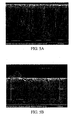
- Figures 4A and 4B show an x-ray diffraction analysis of and an SEM photograph of a LiCoO 2 film deposited according to embodiments of the present invention.
- FIGS 5A through 5E show SEM photographs of LiCoO 2 films according to some embodiments of the present invention.
- Figure 6A illustrates a layer of LiCoO 2 deposited according to some embodiments of the present invention on a thin substrate.
- Figure 6B illustrates a layer of LiCoO 2 deposited according to some embodiments of the present invention over a conducting layer on a thin substrate.
- Figures 7A , 7B , 7C , and 7D illustrate a thin substrate mount and mask arrangement that can be utilized in the deposition of LiCoO 2 layers deposited according to some embodiments of the present invention.
- Figure 8 illustrates a cluster tool that can be utilized to form batteries with LiCoO 2 layers deposited according to some embodiments of the present invention.
- Figures 9A and 9B illustrate examples of stacked batter structures with LiCoO 2 layers deposited according to some embodiments of the present invention.
- Figures 10A through 10D illustrate deposition and anneal steps for LiCoO 2 deposited over an iridium layer on a silicon wafer.
- FIGS 11A through 11D illustrate a single layer battery formed over an iridium layer according to some embodiments of the present invention.
- Figure 12 illustrates battery performance utilizing films deposited according to some embodiments of the present invention.
- LiCoO 2 films are deposited on a substrate by a pulsed-dc physical vapor deposition (PVD) process.
- PVD pulsed-dc physical vapor deposition
- LiCoO 2 films according to some embodiments of the present invention provide a crystalline LiCoO 2 film as deposited on a substrate at a substrate temperature as low as about 220 °C during deposition, without the use of a metallic nucleation or barrier underlying film.
- the as-deposited crystalline LiCoO 2 films can be easily ripened to very high crystalline condition by anneal.
- the as deposited crystalline films when positioned on a noble metal film can be annealed at much further reduced temperatures, for example as low as 400 to 500 °C instead of 700 °C, providing for deposition, annealing, and production of solid state batteries on lower temperature substrates.
- films deposited according to the present invention can have a deposition rate of from about 10 to about 30 times higher than processes in conventional films. Deposition thicknesses and times of deposition for films deposited according to the present invention are illustrated in Table I. Furthermore, films according to the present invention can be deposited on wide area substrates having a surface area from 10 to 50 times the surface area of prior sputtering processes, resulting in much higher productivity and much lower cost of manufacture, thereby providing high-volume, low-cost batteries.
- deposition processes without ion sources are capable of depositing amorphous LiCoO 2 layers, but do not deposit crystalline LiCoO 2 layers.
- depositions according to some embodiment of the present invention deposit a LiCoO 2 layer with substantial crystallinity readily measured by x-ray diffraction techniques.
- the crystallinity of the as-deposited LiCoO 2 layers is sufficient to be utilized in a battery structure with no further thermal processing.
- crystallinity of the as-deposited LiCoO 2 layers are improved by thermal processes with low thermal budgets, which can be compatible with films deposited on low-temperature substrates.
- the stoichiometry of some LiCoO 2 layers deposited according to some embodiments of the present invention shows that this layer is sufficient for utilization in a battery.
- a battery utilizing as-deposited LiCoO 2 films can be produced. Heat treating the LiCoO 2 layers may improve the crystallinity and lower the impedance.
- a crystalline layer of LiCoO 2 with a ⁇ 101> or a ⁇ 003> crystalline orientation is deposited directly on the substrate.
- Deposition of crystalline material can eliminate or lessen the need of a subsequent high temperature anneal or precious-metal layers to crystallize and orient the film. Removing the high temperature anneal allows for formation of battery structures on light-weight and low temperature substrates such as stainless steel foil, copper foil, aluminum foil, and plastic sheet, reducing both the weight and the cost of batteries while retaining the energy density storage capabilities of Li-based batteries.
- a crystalline LiCoO 2 layer can be deposited on a precious metal layer, such as iridium, resulting in a further significant lowering of the ripening thermal budget required to improve crystallinity.
- 10/101,341 are each assigned to the same assignee as is the present disclosure and each is incorporated herein in their entirety.
- Deposition of oxide materials has also been described in U.S. Patent No. 6,506,289 , which is also herein incorporated by reference in its entirety.
- Transparent oxide films can be deposited utilizing processes similar to those specifically described in U.S. Patent No. 6,506,289 and U.S. Application Serial No. 10/101863 .
- FIG. 1A shows a schematic of a reactor apparatus 10 for sputtering material from a target 12 according to the present invention.
- apparatus 10 may, for example, be adapted from an AKT-1600 PVD (400 X 500 mm substrate size) system from Applied Komatsu or an AKT-4300 (600 X 720 mm substrate size) system from Applied Komatsu, Santa Clara, CA.
- the AKT-1600 reactor for example, has three deposition chambers connected by a vacuum transport chamber. These AKT reactors can be modified such that pulsed DC power is supplied to the target and RF power is supplied to the substrate during deposition of a material film.
- Apparatus 10 includes target 12 which is electrically coupled through a filter 15 to a pulsed DC power supply 14.
- target 12 is a wide area sputter source target, which provides material to be deposited on a substrate 16.
- Substrate 16 is positioned parallel to and opposite target 12.
- Target 12 functions as a cathode when power is applied to it from the pulsed DC power supply 14 and is equivalently termed a cathode.
- Application of power to target 12 creates a plasma 53.
- Substrate 16 is capacitively coupled to an electrode 17 through an insulator 54.
- Electrode 17 can be coupled to an RF power supply 18.
- a magnet 20 is scanned across the top of target 12.
- the polarity of the power supplied to target 12 by power supply 14 oscillates between negative and positive potentials.
- the insulating layer on the surface of target 12 is discharged and arcing is prevented.
- the pulsing frequency exceeds a critical frequency that can depend on target material, cathode current and reverse time.
- High quality oxide films can be made using reactive pulse DC magnetron sputtering as shown in apparatus 10.
- Pulsed DC power supply 14 can be any pulsed DC power supply, for example an AE Pinnacle plus 10K by Advanced Energy, Inc. With this DC power supply, up to 10 kW of pulsed DC power can be supplied at a frequency of between 0 and 350 kHz.
- the reverse voltage can be 10% of the negative target voltage. Utilization of other power supplies can lead to different power characteristics, frequency characteristics, and reverse voltage percentages.
- the reverse time on this embodiment of power supply 14 can be adjusted between 0 and 5 ⁇ s.
- Filter 15 prevents the bias power from power supply 18 from coupling into pulsed DC power supply 14.
- power supply 18 can be a 2 MHz RF power supply, for example a Nova-25 power supply made by ENI, Colorado Springs, Co.
- filter 15 can be a 2 MHz sinusoidal band rejection filter.
- the band width of the filter can be approximately 100 kHz. Filter 15, therefore, prevents the 2 MHz power from the bias to substrate 16 from damaging power supply 14 and allow passage of the pulsed-dc power and frequency.
- Pulsed DC deposited films are not fully dense and may have columnar structures.
- Columnar structures can be detrimental to thin film applications such as barrier films and dielectric films, where high density is important, due to the boundaries between the columns.
- the columns act to lower the dielectric strength of the material, but may provide diffusion paths for transport or diffusion of electrical current, ionic current, gas, or other chemical agents such as water.
- a columnar structure containing crystallinity as derived from processes according to the present invention is beneficial for battery performance because it allows better Li transport through the boundaries of the material.
- target 12 can have an active size of about 675.7 X 582.48 mm by 4 to 8 mm in order to deposit films on substrate 16 that have dimension about 400 X 500 mm.
- the temperature of substrate 16 can be adjusted to between -50 °C and 500 °C.
- the distance between target 12 and substrate 16 can be between about 3 and about 9 cm (in some embodiments, between 4.8 and 6 cm are used).
- Process gas can be inserted into the chamber of apparatus 10 at a rate up to about 200 sccm while the pressure in the chamber of apparatus 10 can be held at between about .7 and 6 milliTorr.
- Magnet 20 provides a magnetic field of strength between about 400 and about 600 Gauss directed in the plane of target 12 and is moved across target 12 at a rate of less than about 20-30 sec/scan.
- magnet 20 can be a race-track shaped magnet with dimensions about 150 mm by 600 mm.
- Figure 2 illustrates an example of target 12.
- a film deposited on a substrate positioned on carrier sheet 17 directly opposed to region 52 of target 12 has good thickness uniformity.
- Region 52 is the region shown in Figure 1B that is exposed to a uniform plasma condition.
- carrier 17 can be coextensive with region 52.
- Region 24 shown in Figure 2 indicates the area below which both physically and chemically uniform deposition can be achieved, for example where physical and chemical uniformity provide refractive index uniformity, oxide film uniformity, or metallic film uniformity.
- Figure 2 indicates region 52 of target 12 that provides thickness uniformity, which is, in general, larger than region 24 of target 12 providing thickness and chemical uniformity to the deposited film. In optimized processes, however, regions 52 and 24 may be coextensive.
- magnet 20 extends beyond area 52 in one direction, for example the Y direction in Figure 2 , so that scanning is necessary in only one direction, for example the X direction, to provide a time averaged uniform magnetic field.
- magnet 20 can be scanned over the entire extent of target 12, which is larger than region 52 of uniform sputter erosion. Magnet 20 is moved in a plane parallel to the plane of target 12.
- the combination of a uniform target 12 with a target area 52 larger than the area of substrate 16 can provide films of highly uniform thickness. Further, the material properties of the film deposited can be highly uniform.
- the conditions of sputtering at the target surface such as the uniformity of erosion, the average temperature of the plasma at the target surface, and the equilibration of the target surface with the gas phase ambient of the process are uniform over a region which is greater than or equal to the region to be coated with a uniform film thickness.
- the region of uniform film thickness is greater than or equal to the region of the film which is to have highly uniform electrical, mechanical, or optical properties such as index of refraction, stoichiometry, density, transmission, or absorptivity.
- Target 12 can be formed of any materials that provide the correct stoichiometry for LiCoO 2 deposition. Typical ceramic target materials include oxides of Li and Co as well as metallic Li and Co additions and dopants such as Ni, Si, Nb, or other suitable metal oxide additions. In the present disclosure, target 12 can be formed from LiCoO 2 for deposition of LiCoO 2 film.
- material tiles are formed. These tiles can be mounted on a backing plate to form a target for apparatus 10.
- a wide area sputter cathode target can be formed from a close packed array of smaller tiles.
- Target 12 may include any number of tiles, for example between 2 and 60 individual tiles.
- Tiles can be finished to a size so as to provide a margin of edge-wise non-contact, tile to tile, less than about 0.010" to about 0.020" or less than half a millimeter so as to eliminate plasma processes that may occur between adjacent ones of tiles 30.
- the distance between tiles of target 12 and the dark space anode or ground shield 19 in Figure 1B can be somewhat larger so as to provide non contact assembly or to provide for thermal expansion tolerance during process chamber conditioning or operation.
- a uniform plasma condition can be created in the region between target 12 and substrate 16 in a region overlying substrate 16.
- a plasma 53 can be created in region 51, which extends under the entire target 12.
- a central region 52 of target 12 can experience a condition of uniform sputter erosion.
- a layer deposited on a substrate placed anywhere below central region 52 can then be uniform in thickness and other properties (i.e., dielectric, optical index, or material concentrations).
- target 12 is substantially planar in order to provide uniformity in the film deposited on substrate 16.
- planarity of target 12 can mean that all portions of the target surface in region 52 are within a few millimeters of a planar surface, and can be typically within 0.5 mm of a planar surface.
- FIG 3 shows a battery structure with a LiCoO 2 layer deposited according to some embodiments of the present invention.
- a metallic current collection layer 302 is deposited on a substrate 301.
- current collection layer 302 can be patterned in various ways before deposition of a LiCoO 2 layer 303.
- LiCoO 2 layer 303 can be a deposited crystalline layer.
- layer 303 is crystalline without the necessity of a crystallizing heat treatment.
- substrate 301 can be a silicon wafer, titanium metal, alumina, or other conventional high temperature substrate, but may also be a low temperature material such as plastic, glass, or other material which could be susceptible to damage from the high temperature crystallizing heat treatment.
- This feature can have the great advantage of decreasing the expense and weight of battery structures formed by the present invention.
- the low temperature deposition of the LiCoO 2 allows for successive depositions of battery layers, one upon another. Such a process would have the advantage that successive layers of battery structure would be obtained in a stacked condition without the inclusion of a substrate layer.
- the stacked layered battery would provide higher specific energy density as well as low impedance operation for charging and discharging.
- an oxide layer can be deposited on substrate 301.
- a silicon oxide layer can be deposited on a silicon wafer.
- Other layers can be formed between conducting layer 302 and substrate 301.
- a LiPON layer 304 (Li x PO y N z ,) is deposited over LiCoO 2 layer 303.
- LiPON layer 304 is the electrolyte for battery 300 while LiCoO 2 layer 303 acts as the cathode.
- a metallic conducting layer 305 can be deposited over the LiPON layer 304 in order to complete the battery.
- Metallic conducting layer 305 can include lithium adjacent to LiPON layer 304.
- An anode 305 is deposited over LiPON layer 304.
- Anode 305 can be, for example an evaporated lithium metal. Other materials such as, for example, nickel can also be utilized.
- a current collector 306, which is a conducting material, is then deposited over at least a portion of anode 305.
- a Li based thin film battery operates by transport of Li ions in the direction from current collector 306 to current collector 302 in order to hold the voltage between current collector 306 and current collector 302 at a constant voltage.
- the ability for battery structure 300 to supply steady current depends on the ability of Li ions to diffuse through LiPON layer 304 and LiCoO 2 layer 303.
- Li transport through bulk cathode LiCoO 2 layer 303 in a thin film battery occurs by the way of grains or grain boundaries.
- LiCoO 2 layer 303 should include crystals oriented in the ⁇ 101> direction or ⁇ 003> direction.
- LiCoO 2 films can be deposited on substrate 302 with a pulsed-DC biased PVD system as was described above.
- an AKT 1600 PVD system can be modified to provide an RF bias and an Advanced Energy Pinnacle plus 10K pulsed DC power supply can be utilized to provide power to a target.
- the pulsing frequency of the power supply can vary from about 0 to about 350 KHz.
- the power output of the power supply is between 0 and about 10 kW.
- a target of densified LiCoO 2 tiles having a resistivity in the range of about 3 to about 10 k ⁇ can be utilized with dc-sputtering.
- LiCoO 2 films are deposited on Si wafers.
- Gas flows containing Oxygen and Argon can be utilized.
- the Oxygen to Argon ratio ranges from 0 to about 50% with a total gas flow of about 80 sccm.
- the pulsing frequency ranges from about 200 kHz to about 300 kHz during deposition.
- RF bias can also be applied to the substrate. In many trials, the deposition rates vary from about 2 Angstrom/(kW sec) to about 1 Angstrom/(kW sec) depending on the O 2 /Ar ratio as well as substrate bias.
- Table I illustrates some example depositions of LiCoO 2 according to the present invention.
- XRD x-Ray Diffraction
- results taken on the resulting thin films illustrate that films deposited according to the present invention are crystalline films, often with highly textured grain sizes as large as about 150 nm. The dominant crystal orientation appears to be sensitive to the O 2 /Ar ratio.
- O 2 /Ar ratios ⁇ 10%, as-deposited films exhibit a preferred orientation in the ⁇ 101> direction or the ⁇ 003> direction with poorly developed ⁇ 003> planes.
- Figures 4A and 4B illustrate an XRD Analysis and SEM cross section, respectively, of the LiCoO 2 film deposited as Example 15 in Table I.
- a LiCoO 2 film was deposited on Si wafer with 2kW of target power, a frequency of 300 kHz, with 60 sccm Ar and 20 sccm of O 2 for a substrate with an initial temperature of about 30°C.
- a strong ⁇ 101> peak is indicated showing a strong orientation of LiCoO 2 crystals in the desired ⁇ 101> crystallographic direction.
- the SEM cross section shown in Figure 4B further shows the columnar structure of the film having the ⁇ 101> direction and the grain boundaries of the resulting LiCoO 2 crystals.
- FIGS 5A through 5E show SEM cross sections of further example depositions of LiCoO 2 crystals according to the present invention.
- deposition of the LiCoO 2 film was performed on a Si wafer with target power of about 2 kW and frequency of about 250 kHz.
- the LiCoO 2 film shown in Figure 5A corresponds to the example deposition Example 1 in Table I.
- no bias power was utilized with an argon flow rate of about 80 sccm and an oxygen flow rate of about 0 sccm.
- a deposition rate of about 1.45 ⁇ m/hr was achieved over the full substrate area of 400 X 500 mm.
- a ⁇ 101> orientation of the LiCoO 2 was achieved.
- the rate of deposition of the LiCoO 2 layer shown in Figure 5A is very high, likely due to the relatively high conductivity or low resistivity of the ceramic LiCoO 2 oxide sputter target.
- a target resistance of 10 kOhms was measured by means of an Ohm meter over a distance of about 4 cm on the surface of target 12. This high rate allows the manufacture of the 3 micron or thicker LiCoO 2 layer required for the battery at high rate over a wide area in short times, resulting in very high productivity and very low cost.
- Target resistance on the order of about 500 k ⁇ over the same distance by the same measurement technique or higher would not allow for such a high sputter efficiency or high rate of deposition at such a low target power.
- the resistance of conventional target materials can be unmeasurably high.
- a resistance of 100 k ⁇ over about 4 cm of surface will result in high sputter efficiency and high rate of deposition. Further, because deposition rates typically scale nearly linearly with target power, a deposition at 6 kW will yield a deposition rate of approximately 3 ⁇ m/hr, which is a very desirable rate of deposition for manufacturability of Li-based thin-film solid-state batteries on a surface area of 400 X 500 mm 2 .
- the LiCoO 2 layer shown in Figure 5B is deposited under the conditions listed as Example 7 in Table I. Again, no bias was utilized in the deposition. An argon flow rate of about 72 sccm and an oxygen flow rate of about 8 sccm was utilized. The deposition rate was significantly reduced to about 0.85 ⁇ m/hr. Further, although a ⁇ 101> crystallinity can be discerned, that ⁇ 101> crystallinity is not as pronounced as that exhibited in the deposition of the film shown in Figure 5A .
- the LiCoO 2 film shown in Figure 5C was deposited according to Example 3 in Table I. In this deposition, 100 W of bias power is applied to the substrate. Further, an argon flow rate of 72 sccm, and an oxygen flow rate of 8 sccm was utilized. The deposition rate was about 0.67 ⁇ m/hr. Therefore, the application of bias in comparison with the LiCoO 2 film shown in Figure 5B further reduced the deposition rate (from 0.85 ⁇ m/hr of the example shown in Figure 5B to 0.67 ⁇ m/hr of the example shown in Figure 5C ). Further, the desired ⁇ 101> directionality of formed crystals appears to be further degraded.
- the LiCoO 2 film shown in Figure 5D corresponds to Example 4 in Table I.
- the Ar/O 2 ratio was increased.
- increasing the Ar/O 2 ratio improves crystallinity.
- the deposition illustrated in Figure 5D was performed with an argon flow of about 76 sccm and an oxygen flow of about 4 sccm as well as retaining the 100 W bias to the substrate.
- the LiCoO 2 deposition rate was improved to 0.79 ⁇ m/hr from a rate of 0.67 ⁇ m/hr illustrated in Figure 5C .
- Example 6 of Table I the argon flow rate was set at about 74 sccm and the oxygen flow rate was set at about 6 sccm, resulting in a LiCoO 2 deposition rate of about 0.67 ⁇ m/hr. Therefore, increasing both argon and oxygen flow rate over the deposition illustrated in Figure 5E resulted in a lower deposition rate.
- FIG. 6A illustrates a layer of LiCoO 2 602 deposited on a thin substrate 601 according to some embodiments of the present invention.
- Higher lithium-ion mobilities can be achieved utilizing crystalline LiCoO 2 cathode films 602 deposited on a thin substrate 601 that has thickness comparable to that of the battery stack itself, rather than a thickness many or tens of times that of the battery stack. Such a film can lead to faster charging and discharging rates.
- Substrate 601 can be formed of a thin metallic sheet (e.g., aluminum, titanium, stainless steel, or other suitable thin metallic sheet), can be formed of a polymer or plastic material, or may be formed of a ceramic or glass material.
- a conducting layer 603 can be deposited between substrate 601 and LiCoO 2 layer 602.
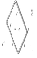
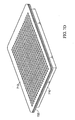
- FIGs 7A , 7B , 7C , and 7D illustrate a reusable fixture 700 for holding a thin film substrate.
- reusable fixture 700 includes a top portion 701 and a bottom portion 702 that snap together.
- Thin substrate 601 is positioned between top portion 701 and bottom portion 702.
- top portion 701 and bottom portion 702 are such that substrate 601 is brought into tension and subsequently clamped as top portion 701 is closed into bottom portion 702.
- Substrate 601 can be easily held by fixture 700 so that substrate 601 can be handled and positioned.
- the corners of substrate 601, areas 703, are removed so that substrate 601 is more easily stretched by avoiding "wrap-around" corner clamping effects when top portion 701 is closed into bottom portion 702.
- a mask 712 can be attached to fixture 700.
- fixture 700 includes guides in order to align fixture 700 with respect to mask 712.
- mask 712 may be attached to fixture 700 and travel with fixture 700.
- Mask 712 can be positioned at any desired height above substrate 601 in fixture 700. Therefore, mask 712 can function as either a contact or proximity mask.
- mask 712 is formed of another thin substrate mounted in a fixture similar to fixture 700.
- fixture 700 and mask 712 can be positioned relative to mount 710.
- Mount 710 for example, can be a susceptor, mount, or an electrostatic chuck of a processing chamber such as that shown in Figures 1A and 1B .
- Fixture 700 and mask 712 can have features that allow for ready alignment with respect to each other and with respect to mount 710.
- mask 712 is resident in the processing chamber and aligned with fixture 700 during positioning of fixture 700 on mount 710, as shown in Figure 7D .
- fixture 700 allows processing of a thin film substrate in a processing chamber.
- thin film substrates can be about 10 ⁇ m or more.
- thin film substrate 601, once mounted within fixture 700, can be handled and moved from process chamber to process chamber. Therefore, a multiprocessor chamber system can be utilized to form stacks of layers, including one or more layers of LiCoO 2 deposited according to embodiments of the present invention.
- FIG 8 illustrates a cluster tool 800 for processing thin film substrates.
- Cluster tool 800 can, for example, include load lock 802 and load lock 803, through which mounted thin film substrate 601 is loaded and a resultant device is removed from cluster tool 800.
- Chambers 804, 805, 806, 807, and 808 are processing chambers for depositions of materials, heat treatments, etching, or other processes.
- One or more of chambers 804, 805, 806, 807, and 808 can be a pulsed-DC PVD chamber such as that discussed above with respect to Figures 1A and 1B and within which a LiCoO 2 film deposited according to embodiments of the present invention may be deposited.
- Transfer chamber 801 includes substrate transfer robotics to shuttle individual wafers between processing chambers 804, 805, 806, 807, and 808 and load locks 802 and 803.
- ceramic substrates are loaded into load lock 803.
- a thin metallic layer can be deposited in chamber 804, followed by a LiCoO 2 deposition performed in chamber 805.
- the substrate is then removed through load lock 803 for an in-air heat treatment external to cluster tool 800.
- the treated wafer is then reloaded into cluster tool 800 through load lock 802.
- a LiPON layer can be deposited in chamber 806.
- the wafer is then again removed from cluster tool 800 for deposition of the lithium anode layer, or sometimes chamber 807 can be adapted to deposition of the lithium anode layer.
- a second metallic layer is deposited in chamber 808 to form a charge collector and anode collector.
- the finished battery structure is then off-loaded from cluster tool 800 in load lock 802. Wafers are shuttled from chamber to chamber by robotics in transfer chamber 801.
- a battery structure produced according to the present invention could utilize thin film substrates loaded in a fixture such as fixture 700. Fixture 700 is then loaded into load lock 803. Chamber 804 may still include deposition of a conducting layer. Chamber 805 then includes deposition of a LiCoO 2 layer according to embodiments of the present invention. A LiPON layer can then be deposited in chamber 806. Chamber 807 may still be adapted to deposition of a lithium rich material such as lithium metal and chamber 808 can be utilized for deposition of the conducting layer of the current collector. In this process, no heat treatment is utilized to crystallize the LiCoO 2 layer.
- substrates loaded into cluster tool 800 may traverse process chambers 804, 805, 806, 807, and 808 multiple times in order to produce multiply stacked battery structures.
- Figures 9A and 9B illustrate such battery structures.
- Figure 9A illustrates a parallel coupled stacking.
- a substrate 601 which for example can be a plastic substrate, is loaded into load lock 803.
- Conducting layer 603, for example, can be deposited in chamber 804.
- a LiCoO 2 layer 602 is then deposited on conducting layer 603.
- LiCoO 2 layer 602 can be about.3-10 ⁇ m and can be deposited in chamber 805 according to embodiments of the present invention.
- the wafer can then be moved to chamber 806 where a LiPON layer 901 of thickness of about .5 to about 2 ⁇ m can be deposited.
- an anode layer 902 for example a lithium metal layer of up to about 10 ⁇ m, can then be deposited in chamber 807.
- a second conducting layer 903 can then be deposited over anode layer 902.
- a second battery stack can then be deposited over the first battery stack formed by metal layer 603, LiCoO2 layer 602, LiPON layer 901, lithium layer 902, and current collection conduction layer 903. Over current collection conducting layer 903, another lithium layer 902 is formed.
- Another LiPON layer 901 is formed over lithium layer 902.
- Another LiCoO2 layer 602 is formed over LiPON layer 901 and finally another metal layer 603 is formed over LiCoO2 layer 602.
- further stackings can be formed.
- metal layers 603 and 903 differ in the mask utilized in deposition so that tabs are formed for electrical coupling of layers.
- any number of individual battery stacks can be formed such that parallel battery formations are formed.
- Such a parallel arrangment of battery stacking structure can be indicated as Current collector/LiCoO2/LiPON/Anode/current collector/Anode/LiPON/LiCoO2/current collector/LiCoO2 ... /current collector.
- Figure 9B illustrates an alternative stacking corresponding to the battery structure current collector/LiCo02/LiPON/anode/current collector/LiCo02/LiPON/anode/current collector ... /current collector.
- a series arrangement battery stacking structure is formed because the individual battery stacks share anodes.
- substrates are rotated again through the chambers of cluster tool 800 in order to deposit the multiple sets of batteries.
- a stack of any number of batteries can be deposited in this fashion.
- stoichiometric LiCoO 2 can be deposited on iridium.
- Figures 10A through 10D illustrate an anneal procedure for Li-Co deposition over an iridium layer that has been deposited on a Si wafer.
- the LiCoO 2 deposition was accomplished as discussed above with a target power of 2 kW, no bias power, reverse time of 1.6 ⁇ s, a pulsing frequency of 300 kHz, with 60 sccm Ar flow and 20 sccm of O 2 flow, with no pre-heat for 7200 sec.
- a layer of LiCoO 2 of about 1.51 ⁇ m was deposited.
- FIGS 10A through 10D show XRD analysis of both as-deposited and annealed layers of LiCoO 2 deposited as discussed above.
- the position of the ⁇ 101> LiCoO 2 peak indicates that the ⁇ 101> LiCoO 2 peak is nonstoichiometric LiCoO 2 .
- stoichiometric LiCoO 2 provides for the best Li transport.
- careful adjustment of deposition parameters can provide stoichiometric LiCoO 2 of desired orientation.
- Figure 10B shows an XRD analysis of the sample shown in figure 10A after a 300°C anneal in air for 2 hours.
- the XRD peak corresponding to ⁇ 003> LiCoO 2 grows, indicating crystallization of LiCoO 2 into the ⁇ 003> direction.
- the crystalline LiCoO 2 is still not stoichiometric after this anneal.
- Figure 10D illustrates an XRD analsysis of the sample after a subsequent anneal of 700°C in air for 2 hours.
- the ⁇ 003> LiCoO 2 peak disappears, but the ⁇ 012> LiCoO 2 peak remains relatively the same as that shown in the 500° anneal illustrated in Figure 10C .
- Figures 10A through 10D demonstrate deposition of ⁇ 101> LiCoO 2 at low temperature over an iridium layer. Subsequent anneals to 500°C may be desired to change the stoichiometry of the ⁇ 101> LiCoO 2 layer, but anneals to 700 °C do not appear to be necessary. With anneal temperatures less than 500°C, depositions of a LiCoO 2 layer over a conducting iridium layer can be accomplished on glass, aluminum foil, plastic, or other low temperature substrate material. Anneal temperatures of less than 500°C but greater than 300°C or lengthening the time of lower temperature anneals may also result in desired orientations of stoichiometric crystalline LiCoO 2 .
- FIGS 11A through 11D illustrate formation of a single-layer battery according to some embodiments of the present invention.
- a lift-off layer 1102 can be deposited on a substrate 1101.
- an iridium layer 1103 can be deposited over lift-off layer 1102.
- substrate 1101 can be plastic, glass, A1 foil, Si wafer, or any other material.
- Lift-off layer 1102 can be any lift off layer and can be a polymer layer such as polyimide, an inorganic layer such as CaF 2 or carbon, or an adhesive layer that loses its adhesion as a result of, for example, oxidation, heat, or light. Lift-off layers are well known.
- Iridium layer 1103 can be from about 500 ⁇ or more.
- a LiCoO 2 layer is deposited over iridium layer 1103 as was discussed above.
- an anneal can be performed at this step.
- further layers of the battery may be deposited before an anneal step is performed.
- a stoichiometric LiCoO 2 layer of a useful crystalline orientation may result in the as-deposited LiCoO 2 with no further anneals necessary.
- Figure 11C illustrates deposition of a LiPON layer 1105 over the LiCoO 2 layer, deposition of a Li layer 1106 over LiPON layer 1105, and deposition of an electrode layer 1107 over Li layer 1106.
- an anneal step of up to 500°C as discussed above may be performed here.
- the resulting single-layer battery formed from iridium layer 1103, LiCoO 2 layer 1104, LiPON layer 1105, Li layer 1106, and electrode layer 1107 can be "lifted off' from substrate 1101.
- Such a single-layer battery can be a free-standing battery of thickness about 5 ⁇ m or greater.
- Such a battery, without the requirement of a substrate 1101, is well known to have the potential of energy storage of greater than about 1 kW-hr/liter.
- a substrate may be removed during anneal leaving a single-layer battery.
- substrate 1101 can be removed by a solvent, etching, or a photo process.
- single-layer batteries may be combined or stacked in any fashion to provide a device of greater energy storage at a particular voltage.
- Figure 12A illustrates an XRD analysis of the as-deposited LiCoO 2 film on Al 2 O 3 substrate (Example 32 in Table I). A broad ⁇ 003> crystalline LiCoO 2 peak is observed. The remaining peaks in the analysis, which are not labeled in Figure 12A , result from the Al 2 O 3 substrate. The ⁇ 003> peak is characteristic of the layered structure in the as-deposited crystalline LiCoO 2 film according to embodiments of the present invention.
- Figure 12B illustrates the crystallinity of the LiCoO2 film shown in Figure 12A after a 2 hr 700 °C anneal.
- the ⁇ 003> peak becomes sharper and higher, indicating better crystallinity.
- Figures 12G through 12J in comparison with figures 12C through 12F , the columnar structure ripens with the anneal and the grain size becomes larger with anneal.
- Figure 12B also shows ⁇ 012> and ⁇ 006> crystallinity peaks.
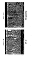
- Figure 12C through 12F show SEM photos of the granularity of the as-deposited film corresponding to Example 32 in Figure I.
- Figures 12G through 12J show SEM photos of the granularity of the annealed film, as illustrated in Figure 12B .
- a comparison of Figures 12C through 12F with 12G through 12J illustrate the increased granularity resulting from the anneal process.
- Figure 12K illustrates a fracture cross-section SEM that illustrates the morphology of the as-deposited crystalline film corresponding to Example 31 in Table I.
- Figure 12L illustrate a similar cross-section SEM corresponding to the film grown according to Example 32 in Table I.
Landscapes
- Chemical & Material Sciences (AREA)
- Engineering & Computer Science (AREA)
- Chemical Kinetics & Catalysis (AREA)
- Electrochemistry (AREA)
- General Chemical & Material Sciences (AREA)
- Manufacturing & Machinery (AREA)
- Materials Engineering (AREA)
- Mechanical Engineering (AREA)
- Metallurgy (AREA)
- Organic Chemistry (AREA)
- Physics & Mathematics (AREA)
- Inorganic Chemistry (AREA)
- Condensed Matter Physics & Semiconductors (AREA)
- General Physics & Mathematics (AREA)
- Thermal Sciences (AREA)
- Composite Materials (AREA)
- Secondary Cells (AREA)
- Battery Electrode And Active Subsutance (AREA)
- Inorganic Compounds Of Heavy Metals (AREA)
- Physical Vapour Deposition (AREA)
- Cell Electrode Carriers And Collectors (AREA)
Abstract
Description
- The present application claims priority to Provisional Application No.
60/651,363, filed on February 8, 2005, by Hongmei Zhang and Richard E. Demaray 60/634,818, filed on December 8, 2004 - The present invention is related to thin-film solid-state batteries and, in particular, the deposition of LiCoO2 films and layers for battery manufacture.
- Solid-state thin-film batteries are typically formed by stacking thin films on a substrate in such a way that the films cooperate to generate a voltage. The thin films typically include current collectors, a cathode, an anode, and an electrolyte. The thin films can be deposited utilizing a number of deposition processes, including sputtering and electroplating. Substrates suitable for this application have conventionally been high temperature materials capable of withstanding at least one high temperature anneal process to at least 700 °C for up to about 2 hours in air so as to crystallize the LiCoO2 film. Such a substrate can be any suitable material with appropriate structural and material properties, for example a semiconductor wafer, metallic sheet (e.g., titanium or zirconium), ceramic such as alumina, or other material capable of withstanding subsequent high temperature processing in the presence of the LiCoO2, which can experience significant interfacial reactions with most materials utilized in a battery during these temperature cycles.
- Other lithium containing mixed metal oxides besides LiCoO2, including Ni, Nb, Mn, V, and sometimes also Co, but including other transition metal oxides, have been evaluated as crystalline energy storage cathode materials. Typically, the cathode material is deposited in amorphous form and then the material is heated in an anneal process to form the crystalline material. In LiCoO2, for example, an anneal at or above 700°C transforms the deposited amorphous film to a crystalline form. Such a high temperature anneal, however, severely limits the materials that can be utilized as the substrate, induces destructive reaction with the lithium containing cathode material and often requires the use of expensive noble metals such as gold. Such high thermal budget processes (i.e., high temperatures for extended periods of time) are incompatible with semiconductor or MEM device processing and limit the choice of substrate materials, increase the cost, and decrease the yield of such batteries.
- It is known that crystallization of amorphous LiCoO2 on precious metals can be achieved. An example of this crystallization is discussed in Kim et al., where a conventional furnace anneal at 700°C for 20 minutes of an amorphous layer of LiCoO2 on a precious metal achieves crystallization of the LiCoO2 material, as shown by x-ray diffraction data. Kim, Han-Ki and Yoon, Young Soo, "Characteristics of rapid-thermal-annealed LiCoO2, cathode film for an all-solid-state thin film microbattery," J. Vac. Sci. Techn. A 22(4), Jul/Aug 2004. In Kim et al., the LiCoO2 film was deposited on a platinum film that was deposited on a high-temperature MgO/Si substrate. In Kim et al, it was shown that such a crystalline film is capable of constituting the Li+ ion containing cathode layer of a functional all solid-state Li+ ion battery.
- There are many references that disclose an ion beam assisted process that can provide a LiCoO2 film that demonstrates some observable crystalline composition by low angle x-ray diffraction (XRD). Some examples of these are found in
U.S. Patent Applications 09/815,983 (Publication No.US 2002/001747 ),09/815,621 US 2001/0032666 ), and09/815,919 US 2002/0001746 ). These references disclose the use of a second front side ion beam or other ion source side-by-side with a deposition source so as to obtain a region of overlap of the flux of ions with the flux of LiCoO2 vapor at the substrate surface. None of these references disclose film temperature data or other temperature data of the film during deposition to support an assertion of low temperature processing. - It is very difficult to form a uniform deposition either by sputtering a material layer or by bombardment with an ion flux. Utilization of two uniform simultaneous distributions from two sources that do not occupy the same position and extent with respect to the substrate enormously increases the difficulties involved in achieving a uniform material deposition. These references do not disclose a uniform materials deposition, which is required for reliable production of thin-film batteries. A well understood specification for material uniformity for useful battery products is that a 5% one-sigma material uniformity is standard in thin film manufacturing. About 86% of the films with this uniformity will be found acceptable for battery production.
- It is even more difficult to scale a substrate to manufacturing scale, such as 200 mm or 300 mm. Indeed, in the references discussed above that utilize both a sputtering deposition and an ion beam deposition, only small area targets and small area substrates are disclosed. These references disclose a single feasibility result. No method for achieving a uniform distribution from two separate front side sources has been disclosed in these references.
- Further, conventional materials and production processes can limit the energy density capacity of the batteries produced, causing a need for more batteries occupying more volume. It is specifically desirable to produce batteries that have large amounts of stored energy per unit volume in order to provide batteries of low weight and low volume.
- Therefore, there is a need for a low temperature process for depositing crystalline material, for example LiCoO2 material, onto a substrate. In particular, there is a need for processes that allow production of cathodic lithium films for a battery structure with a low enough thermal budget to allow production of functional structures on low temperature materials such as stainless steel, aluminum, or copper foil.
According to a first aspect of the invention a method of depositing a LiCoO2 layer, comprises: placing a substrate in a reactor; flowing a gaseous mixture including argon and oxygen through the reactor; and applying pulsed DC power to a target formed of LiCoO2 positioned opposite the substrate, wherein a crystalline layer of LiCoO2 is deposited over the substrate: - According to a second aspect of the invention, the battery structure comprises: a crystalline LiCoO2 layer deposited over a low-temperature substrate remaining at a temperature of less than about 224 °C during the deposition of the crystalline LiCoO2 layer, wherein the crystalline LiCoO2 layer has highly-textured grain sizes between about 750 Å and 1700 Å.
- According to a third aspect of the invention a stacked battery structure, comprises: one or more battery stacks deposited on a thin substrate, wherein each battery stack comprises: a conducting layer, a LiCoO2 layer deposited as a crystalline layer over the conducting layer, wherein the crystalline LiCoO2 layer has highly-textured grain sizes between about 750 Å and 1700 Å; a LiPON layer deposited over the crystalline LiCoO2 layer, an anode layer deposited over the LiPON layer; and a top conducting layer deposited over the one or more battery stacks.
- According to a fourth aspect of the invention a method of producing a battery, comprises: loading a substrate into a cluster tool; depositing a crystalline LiCoO2 layer over a conducting layer in a chamber of the cluster tool with a pulsed-dc PVD process.
- In accordance with the present invention, deposition of LiCoO2 layers in a pulsed-dc physical vapor deposition process is presented. Such a deposition can provide a low-temperature, high deposition rate deposition of a crystalline layer of LiCoO2 with a desired <101> orientation. Some embodiments of the deposition address the need for high rate deposition of LiCoO2 films, which can be utilized as the cathode layer in a solid state rechargeable Li battery. Embodiments of the process according to the present invention can eliminate the high temperature (>700 °C) anneal step that is conventionally needed to crystallize the LiCoO2 layer.
- A method of depositing a LiCoO2 layer according to some embodiment of the present invention includes placing a substrate in a reactor; flowing a gaseous mixture including argon and oxygen through the reactor; and applying pulsed-DC power to a target formed of LiCoO2 positioned opposite the substrate. In some embodiments, a LiCoO2 layer is formed on the substrate. Further, in some embodiments the LiCoO2 layer is a crystalline layer of orientation <101>.
- In some embodiments, a stacked battery structure can be formed. The stacked battery structure includes one or more battery stacks deposited on a thin substrate, wherein each battery stack includes: a conducting layer, a crystalline LiCoO2 layer deposited over the conducting layer, a LiPON layer deposited over the LiCoO2 layer; and an anode deposited over the LiPON layer. A top conducting layer can be deposited over the one or more battery stacks.
- In some embodiments, a battery structure can be formed in a cluster tool. A method of producing a battery in a cluster tool includes loading a substrate into a cluster tool; depositing a conducting layer over the substrate in a first chamber of the cluster tool; depositing a crystalline LiCoO2 layer over the conducting layer in a second chamber of the cluster tool; depositing a LiPON layer over the LiCoO2 layer in a third chamber of the cluster tool; depositing an anode layer over the LiCoO2 layer in a fourth chamber; and depositing a second conducting layer over the LiPON layer in a fifth chamber of the cluster tool.
- A fixture for holding a thin substrate can include a top portion and a bottom portion, wherein the thin substrate is held when the top portion is attached to the bottom portion.
- These and other embodiments of the invention are further discussed below with reference to the following figures. It is to be understood that both the foregoing general description and the following detailed description are exemplary and explanatory only and are not restrictive of the invention, as claimed. Further, specific explanations or theories regarding the deposition or performance of certain layers during deposition processes or in the performance of devices incorporating those layers are presented for explanation only and are not to be considered limiting with respect to the scope of the present disclosure or the claims.
-
Figures 1A and 1B illustrate a pulsed-DC biased reactive deposition apparatus that can be utilized in the methods of depositing according to the present invention. -
Figure 2 shows an example of a target that can be utilized in the reactor illustrated inFigures 1A and 1B . -
Figure 3 illustrates a thin-film battery design according to some embodiments of the present invention. -
Figures 4A and 4B show an x-ray diffraction analysis of and an SEM photograph of a LiCoO2 film deposited according to embodiments of the present invention. -
Figures 5A through 5E show SEM photographs of LiCoO2 films according to some embodiments of the present invention. -
Figure 6A illustrates a layer of LiCoO2 deposited according to some embodiments of the present invention on a thin substrate. -
Figure 6B illustrates a layer of LiCoO2 deposited according to some embodiments of the present invention over a conducting layer on a thin substrate. -
Figures 7A ,7B ,7C , and7D illustrate a thin substrate mount and mask arrangement that can be utilized in the deposition of LiCoO2 layers deposited according to some embodiments of the present invention. -
Figure 8 illustrates a cluster tool that can be utilized to form batteries with LiCoO2 layers deposited according to some embodiments of the present invention. -
Figures 9A and 9B illustrate examples of stacked batter structures with LiCoO2 layers deposited according to some embodiments of the present invention. -
Figures 10A through 10D illustrate deposition and anneal steps for LiCoO2 deposited over an iridium layer on a silicon wafer. -
Figures 11A through 11D illustrate a single layer battery formed over an iridium layer according to some embodiments of the present invention. -
Figure 12 illustrates battery performance utilizing films deposited according to some embodiments of the present invention. - In the figures, elements having the same designation have the same or similar functions.
- In accordance with embodiments of the present invention, LiCoO2 films are deposited on a substrate by a pulsed-dc physical vapor deposition (PVD) process. In contrast to, for example, Kim et al., LiCoO2 films according to some embodiments of the present invention provide a crystalline LiCoO2 film as deposited on a substrate at a substrate temperature as low as about 220 °C during deposition, without the use of a metallic nucleation or barrier underlying film. The as-deposited crystalline LiCoO2 films can be easily ripened to very high crystalline condition by anneal. In addition, the as deposited crystalline films, when positioned on a noble metal film can be annealed at much further reduced temperatures, for example as low as 400 to 500 °C instead of 700 °C, providing for deposition, annealing, and production of solid state batteries on lower temperature substrates.
- In the present application, a single, extended source is described which has been scaled to 400mm X 500mm for production achieving a high LiCoO2 uniformity at a deposition rate of 1.2 microns thickness an hour over an area of 2000 cm2, without the need for secondary front side ion source or ion assistance.
- On other depositions utilizing this process, a temperature measurement of the substrate during deposition showed that the substrate remained at less than 224 °C. Temperature measurements were performed utilizing a temperature sticker purchased from Omega Engineering, Stamford, Ct (Model no. TL-F-390, active from 199-224 °C).
- Moreover, in some embodiments, films deposited according to the present invention can have a deposition rate of from about 10 to about 30 times higher than processes in conventional films. Deposition thicknesses and times of deposition for films deposited according to the present invention are illustrated in Table I. Furthermore, films according to the present invention can be deposited on wide area substrates having a surface area from 10 to 50 times the surface area of prior sputtering processes, resulting in much higher productivity and much lower cost of manufacture, thereby providing high-volume, low-cost batteries.
- Further, conventional deposition processes without ion sources are capable of depositing amorphous LiCoO2 layers, but do not deposit crystalline LiCoO2 layers. Surprisingly, depositions according to some embodiment of the present invention, deposit a LiCoO2 layer with substantial crystallinity readily measured by x-ray diffraction techniques. In some embodiments, the crystallinity of the as-deposited LiCoO2 layers is sufficient to be utilized in a battery structure with no further thermal processing. In some embodiments, crystallinity of the as-deposited LiCoO2 layers are improved by thermal processes with low thermal budgets, which can be compatible with films deposited on low-temperature substrates.
- Further, as-deposited the stoichiometry of some LiCoO2 layers deposited according to some embodiments of the present invention shows that this layer is sufficient for utilization in a battery. With the demonstrated ability to deposit a LiCoO2 film with crystallinity and with sufficient stoichiometry, a battery utilizing as-deposited LiCoO2 films can be produced. Heat treating the LiCoO2 layers may improve the crystallinity and lower the impedance.
- In some embodiments, a crystalline layer of LiCoO2 with a <101> or a <003> crystalline orientation is deposited directly on the substrate. Deposition of crystalline material can eliminate or lessen the need of a subsequent high temperature anneal or precious-metal layers to crystallize and orient the film. Removing the high temperature anneal allows for formation of battery structures on light-weight and low temperature substrates such as stainless steel foil, copper foil, aluminum foil, and plastic sheet, reducing both the weight and the cost of batteries while retaining the energy density storage capabilities of Li-based batteries. In some embodiments, a crystalline LiCoO2 layer can be deposited on a precious metal layer, such as iridium, resulting in a further significant lowering of the ripening thermal budget required to improve crystallinity.
- Deposition of materials by pulsed-DC biased reactive ion deposition is described in
U.S. Patent Application Serial No. 10/101863 U.S. Patent Application Serial No. 10/101,341 U.S. Patent Application Serial No. 10/101863 andU.S. Patent Application Serial No. 10/101,341 are each assigned to the same assignee as is the present disclosure and each is incorporated herein in their entirety. Deposition of oxide materials has also been described inU.S. Patent No. 6,506,289 , which is also herein incorporated by reference in its entirety. Transparent oxide films can be deposited utilizing processes similar to those specifically described inU.S. Patent No. 6,506,289 andU.S. Application Serial No. 10/101863 . -
Figure 1A shows a schematic of areactor apparatus 10 for sputtering material from atarget 12 according to the present invention. In some embodiments,apparatus 10 may, for example, be adapted from an AKT-1600 PVD (400 X 500 mm substrate size) system from Applied Komatsu or an AKT-4300 (600 X 720 mm substrate size) system from Applied Komatsu, Santa Clara, CA. The AKT-1600 reactor, for example, has three deposition chambers connected by a vacuum transport chamber. These AKT reactors can be modified such that pulsed DC power is supplied to the target and RF power is supplied to the substrate during deposition of a material film. -
Apparatus 10 includestarget 12 which is electrically coupled through afilter 15 to a pulsedDC power supply 14. In some embodiments,target 12 is a wide area sputter source target, which provides material to be deposited on asubstrate 16.Substrate 16 is positioned parallel to andopposite target 12.Target 12 functions as a cathode when power is applied to it from the pulsedDC power supply 14 and is equivalently termed a cathode. Application of power to target 12 creates aplasma 53.Substrate 16 is capacitively coupled to anelectrode 17 through aninsulator 54.Electrode 17 can be coupled to anRF power supply 18. Amagnet 20 is scanned across the top oftarget 12. - For pulsed reactive dc magnetron sputtering, as performed by
apparatus 10, the polarity of the power supplied to target 12 bypower supply 14 oscillates between negative and positive potentials. During the positive period, the insulating layer on the surface oftarget 12 is discharged and arcing is prevented. To obtain arc free deposition, the pulsing frequency exceeds a critical frequency that can depend on target material, cathode current and reverse time. High quality oxide films can be made using reactive pulse DC magnetron sputtering as shown inapparatus 10. - Pulsed
DC power supply 14 can be any pulsed DC power supply, for example an AE Pinnacle plus 10K by Advanced Energy, Inc. With this DC power supply, up to 10 kW of pulsed DC power can be supplied at a frequency of between 0 and 350 kHz. The reverse voltage can be 10% of the negative target voltage. Utilization of other power supplies can lead to different power characteristics, frequency characteristics, and reverse voltage percentages. The reverse time on this embodiment ofpower supply 14 can be adjusted between 0 and 5 µs. -
Filter 15 prevents the bias power frompower supply 18 from coupling into pulsedDC power supply 14. In some embodiments,power supply 18 can be a 2 MHz RF power supply, for example a Nova-25 power supply made by ENI, Colorado Springs, Co. - In some embodiments, filter 15 can be a 2 MHz sinusoidal band rejection filter. In some embodiments, the band width of the filter can be approximately 100 kHz.
Filter 15, therefore, prevents the 2 MHz power from the bias tosubstrate 16 fromdamaging power supply 14 and allow passage of the pulsed-dc power and frequency. - Pulsed DC deposited films are not fully dense and may have columnar structures. Columnar structures can be detrimental to thin film applications such as barrier films and dielectric films, where high density is important, due to the boundaries between the columns. The columns act to lower the dielectric strength of the material, but may provide diffusion paths for transport or diffusion of electrical current, ionic current, gas, or other chemical agents such as water. In the case of a solid state battery, a columnar structure containing crystallinity as derived from processes according to the present invention is beneficial for battery performance because it allows better Li transport through the boundaries of the material.
- In the deposition system, target 12 can have an active size of about 675.7 X 582.48 mm by 4 to 8 mm in order to deposit films on
substrate 16 that have dimension about 400 X 500 mm. The temperature ofsubstrate 16 can be adjusted to between -50 °C and 500 °C. The distance betweentarget 12 andsubstrate 16 can be between about 3 and about 9 cm (in some embodiments, between 4.8 and 6 cm are used). Process gas can be inserted into the chamber ofapparatus 10 at a rate up to about 200 sccm while the pressure in the chamber ofapparatus 10 can be held at between about .7 and 6 milliTorr.Magnet 20 provides a magnetic field of strength between about 400 and about 600 Gauss directed in the plane oftarget 12 and is moved acrosstarget 12 at a rate of less than about 20-30 sec/scan. In some embodiments utilizing the AKT reactor,magnet 20 can be a race-track shaped magnet with dimensions about 150 mm by 600 mm. -
Figure 2 illustrates an example oftarget 12. A film deposited on a substrate positioned oncarrier sheet 17 directly opposed toregion 52 oftarget 12 has good thickness uniformity.Region 52 is the region shown inFigure 1B that is exposed to a uniform plasma condition. In some implementations,carrier 17 can be coextensive withregion 52.Region 24 shown inFigure 2 indicates the area below which both physically and chemically uniform deposition can be achieved, for example where physical and chemical uniformity provide refractive index uniformity, oxide film uniformity, or metallic film uniformity.Figure 2 indicatesregion 52 oftarget 12 that provides thickness uniformity, which is, in general, larger thanregion 24 oftarget 12 providing thickness and chemical uniformity to the deposited film. In optimized processes, however,regions - In some embodiments,
magnet 20 extends beyondarea 52 in one direction, for example the Y direction inFigure 2 , so that scanning is necessary in only one direction, for example the X direction, to provide a time averaged uniform magnetic field. As shown inFigures 1A and 1B ,magnet 20 can be scanned over the entire extent oftarget 12, which is larger thanregion 52 of uniform sputter erosion.Magnet 20 is moved in a plane parallel to the plane oftarget 12. - The combination of a
uniform target 12 with atarget area 52 larger than the area ofsubstrate 16 can provide films of highly uniform thickness. Further, the material properties of the film deposited can be highly uniform. The conditions of sputtering at the target surface, such as the uniformity of erosion, the average temperature of the plasma at the target surface, and the equilibration of the target surface with the gas phase ambient of the process are uniform over a region which is greater than or equal to the region to be coated with a uniform film thickness. In addition, the region of uniform film thickness is greater than or equal to the region of the film which is to have highly uniform electrical, mechanical, or optical properties such as index of refraction, stoichiometry, density, transmission, or absorptivity. -
Target 12 can be formed of any materials that provide the correct stoichiometry for LiCoO2 deposition. Typical ceramic target materials include oxides of Li and Co as well as metallic Li and Co additions and dopants such as Ni, Si, Nb, or other suitable metal oxide additions. In the present disclosure,target 12 can be formed from LiCoO2 for deposition of LiCoO2 film. - In some embodiments of the invention, material tiles are formed. These tiles can be mounted on a backing plate to form a target for
apparatus 10. A wide area sputter cathode target can be formed from a close packed array of smaller tiles.Target 12, therefore, may include any number of tiles, for example between 2 and 60 individual tiles. Tiles can be finished to a size so as to provide a margin of edge-wise non-contact, tile to tile, less than about 0.010" to about 0.020" or less than half a millimeter so as to eliminate plasma processes that may occur between adjacent ones oftiles 30. The distance between tiles oftarget 12 and the dark space anode orground shield 19 inFigure 1B can be somewhat larger so as to provide non contact assembly or to provide for thermal expansion tolerance during process chamber conditioning or operation. - As shown in
Figure 1B , a uniform plasma condition can be created in the region betweentarget 12 andsubstrate 16 in aregion overlying substrate 16. Aplasma 53 can be created in region 51, which extends under theentire target 12. Acentral region 52 oftarget 12 can experience a condition of uniform sputter erosion. As discussed further herein, a layer deposited on a substrate placed anywhere belowcentral region 52 can then be uniform in thickness and other properties (i.e., dielectric, optical index, or material concentrations). In some embodiments,target 12 is substantially planar in order to provide uniformity in the film deposited onsubstrate 16. In practice, planarity oftarget 12 can mean that all portions of the target surface inregion 52 are within a few millimeters of a planar surface, and can be typically within 0.5 mm of a planar surface. -
Figure 3 shows a battery structure with a LiCoO2 layer deposited according to some embodiments of the present invention. As shown inFigure 3 , a metalliccurrent collection layer 302 is deposited on asubstrate 301. In some embodiments,current collection layer 302 can be patterned in various ways before deposition of a LiCoO2 layer 303. Also according to some embodiments, LiCoO2 layer 303 can be a deposited crystalline layer. In some embodiments of the invention,layer 303 is crystalline without the necessity of a crystallizing heat treatment. Therefore,substrate 301 can be a silicon wafer, titanium metal, alumina, or other conventional high temperature substrate, but may also be a low temperature material such as plastic, glass, or other material which could be susceptible to damage from the high temperature crystallizing heat treatment. This feature can have the great advantage of decreasing the expense and weight of battery structures formed by the present invention. The low temperature deposition of the LiCoO2 allows for successive depositions of battery layers, one upon another. Such a process would have the advantage that successive layers of battery structure would be obtained in a stacked condition without the inclusion of a substrate layer. The stacked layered battery would provide higher specific energy density as well as low impedance operation for charging and discharging. - In some embodiments, an oxide layer can be deposited on
substrate 301. For example, a silicon oxide layer can be deposited on a silicon wafer. Other layers can be formed betweenconducting layer 302 andsubstrate 301. - As further shown in
Figure 3 , a LiPON layer 304 (LixPOyNz,) is deposited over LiCoO2 layer 303.LiPON layer 304 is the electrolyte forbattery 300 while LiCoO2 layer 303 acts as the cathode. Ametallic conducting layer 305 can be deposited over theLiPON layer 304 in order to complete the battery.Metallic conducting layer 305 can include lithium adjacent toLiPON layer 304. - An
anode 305 is deposited overLiPON layer 304.Anode 305 can be, for example an evaporated lithium metal. Other materials such as, for example, nickel can also be utilized. Acurrent collector 306, which is a conducting material, is then deposited over at least a portion ofanode 305. - A Li based thin film battery operates by transport of Li ions in the direction from
current collector 306 tocurrent collector 302 in order to hold the voltage betweencurrent collector 306 andcurrent collector 302 at a constant voltage. The ability forbattery structure 300 to supply steady current, then, depends on the ability of Li ions to diffuse throughLiPON layer 304 and LiCoO2 layer 303. Li transport through bulk cathode LiCoO2 layer 303 in a thin film battery occurs by the way of grains or grain boundaries. Without being restricted in this disclosure to any particular theory of transport, it is believed that the grains with their planes parallel tosubstrate 302 will block the flow of Li ions while grains oriented with planes perpendicular to substrate 301 (i.e., oriented parallel to the direction of Li ion flow) facilitate the Li diffusion. Therefore, in order to provide a high-current battery structure, LiCoO2 layer 303 should include crystals oriented in the <101> direction or <003> direction. - In accordance with the present invention, LiCoO2 films can be deposited on
substrate 302 with a pulsed-DC biased PVD system as was described above. In addition, an AKT 1600 PVD system can be modified to provide an RF bias and an Advanced Energy Pinnacle plus 10K pulsed DC power supply can be utilized to provide power to a target. The pulsing frequency of the power supply can vary from about 0 to about 350 KHz. The power output of the power supply is between 0 and about 10 kW. A target of densified LiCoO2 tiles having a resistivity in the range of about 3 to about 10 kΩ can be utilized with dc-sputtering. - In some embodiments, LiCoO2 films are deposited on Si wafers. Gas flows containing Oxygen and Argon can be utilized. In some embodiments, the Oxygen to Argon ratio ranges from 0 to about 50% with a total gas flow of about 80 sccm. The pulsing frequency ranges from about 200 kHz to about 300 kHz during deposition. RF bias can also be applied to the substrate. In many trials, the deposition rates vary from about 2 Angstrom/(kW sec) to about 1 Angstrom/(kW sec) depending on the O2/Ar ratio as well as substrate bias.
- Table I illustrates some example depositions of LiCoO2 according to the present invention. XRD (x-Ray Diffraction) results taken on the resulting thin films illustrate that films deposited according to the present invention are crystalline films, often with highly textured grain sizes as large as about 150 nm. The dominant crystal orientation appears to be sensitive to the O2/Ar ratio. For certain O2/Ar ratios (∼10%), as-deposited films exhibit a preferred orientation in the <101> direction or the <003> direction with poorly developed <003> planes.
-
Figures 4A and 4B illustrate an XRD Analysis and SEM cross section, respectively, of the LiCoO2 film deposited as Example 15 in Table I. Such a LiCoO2 film was deposited on Si wafer with 2kW of target power, a frequency of 300 kHz, with 60 sccm Ar and 20 sccm of O2 for a substrate with an initial temperature of about 30°C. As shown in the XRD analysis ofFigure 4A , a strong <101> peak is indicated showing a strong orientation of LiCoO2 crystals in the desired <101> crystallographic direction. The SEM cross section shown inFigure 4B further shows the columnar structure of the film having the <101> direction and the grain boundaries of the resulting LiCoO2 crystals. -
Figures 5A through 5E show SEM cross sections of further example depositions of LiCoO2 crystals according to the present invention. In each of the examples, deposition of the LiCoO2 film was performed on a Si wafer with target power of about 2 kW and frequency of about 250 kHz. The LiCoO2 film shown inFigure 5A corresponds to the example deposition Example 1 in Table I. In the deposition of the LiCoO2 film shown inFigure 5A , no bias power was utilized with an argon flow rate of about 80 sccm and an oxygen flow rate of about 0 sccm. A deposition rate of about 1.45 µm/hr was achieved over the full substrate area of 400 X 500 mm. Further, as is indicated in the cross section shown inFigure 5A , a <101> orientation of the LiCoO2 was achieved. - The rate of deposition of the LiCoO2 layer shown in
Figure 5A is very high, likely due to the relatively high conductivity or low resistivity of the ceramic LiCoO2 oxide sputter target. A target resistance of 10 kOhms was measured by means of an Ohm meter over a distance of about 4 cm on the surface oftarget 12. This high rate allows the manufacture of the 3 micron or thicker LiCoO2 layer required for the battery at high rate over a wide area in short times, resulting in very high productivity and very low cost. Target resistance on the order of about 500 kΩ over the same distance by the same measurement technique or higher would not allow for such a high sputter efficiency or high rate of deposition at such a low target power. The resistance of conventional target materials can be unmeasurably high. A resistance of 100 kΩ over about 4 cm of surface will result in high sputter efficiency and high rate of deposition. Further, because deposition rates typically scale nearly linearly with target power, a deposition at 6 kW will yield a deposition rate of approximately 3 µm/hr, which is a very desirable rate of deposition for manufacturability of Li-based thin-film solid-state batteries on a surface area of 400 X 500 mm2 . - The LiCoO2 layer shown in
Figure 5B is deposited under the conditions listed as Example 7 in Table I. Again, no bias was utilized in the deposition. An argon flow rate of about 72 sccm and an oxygen flow rate of about 8 sccm was utilized. The deposition rate was significantly reduced to about 0.85 µm/hr. Further, although a <101> crystallinity can be discerned, that <101> crystallinity is not as pronounced as that exhibited in the deposition of the film shown inFigure 5A . - The LiCoO2 film shown in
Figure 5C was deposited according to Example 3 in Table I. In this deposition, 100 W of bias power is applied to the substrate. Further, an argon flow rate of 72 sccm, and an oxygen flow rate of 8 sccm was utilized. The deposition rate was about 0.67 µm/hr. Therefore, the application of bias in comparison with the LiCoO2 film shown inFigure 5B further reduced the deposition rate (from 0.85 µm/hr of the example shown inFigure 5B to 0.67 µm/hr of the example shown inFigure 5C ). Further, the desired <101> directionality of formed crystals appears to be further degraded. - The LiCoO2 film shown in
Figure 5D corresponds to Example 4 in Table I. In this deposition, the Ar/O2 ratio was increased. As is shown inFigure 5D , increasing the Ar/O2 ratio improves crystallinity. With respect to the example illustrated inFigure 5C , the deposition illustrated inFigure 5D was performed with an argon flow of about 76 sccm and an oxygen flow of about 4 sccm as well as retaining the 100 W bias to the substrate. The LiCoO2 deposition rate was improved to 0.79 µm/hr from a rate of 0.67 µm/hr illustrated inFigure 5C . - In the example deposition illustrated in
Figure 5E corresponding to Example 5 in Table I. The substrate temperature was set at about 200°C while the bias power remained at about 100 W. The argon flow rate was set at about 76 sccm and the oxygen flow rate was set at about 4 sccm. The resulting deposition rate for the LiCoO2 layer was about 0.74 µm/hr. - In Example 6 of Table I, the argon flow rate was set at about 74 sccm and the oxygen flow rate was set at about 6 sccm, resulting in a LiCoO2 deposition rate of about 0.67 µm/hr. Therefore, increasing both argon and oxygen flow rate over the deposition illustrated in
Figure 5E resulted in a lower deposition rate. - The data show clearly that an as-deposited crystalline film of LiCoO2 can be obtained under several of the process conditions, as shown in Table II. In particular, very high rates of deposition with low power are obtained along with the oriented crystalline structure for the process conditions according to embodiments of the present invention.
-
Figure 6A illustrates a layer ofLiCoO 2 602 deposited on athin substrate 601 according to some embodiments of the present invention. Higher lithium-ion mobilities can be achieved utilizing crystalline LiCoO2 cathode films 602 deposited on athin substrate 601 that has thickness comparable to that of the battery stack itself, rather than a thickness many or tens of times that of the battery stack. Such a film can lead to faster charging and discharging rates.Substrate 601 can be formed of a thin metallic sheet (e.g., aluminum, titanium, stainless steel, or other suitable thin metallic sheet), can be formed of a polymer or plastic material, or may be formed of a ceramic or glass material. As shown inFigure 6B , ifsubstrate 601 is an insulating material, aconducting layer 603 can be deposited betweensubstrate 601 and LiCoO2 layer 602. - Depositing materials on a thin substrate involves holding and positioning the substrate during deposition.
Figures 7A ,7B ,7C , and7D illustrate areusable fixture 700 for holding a thin film substrate. As shown inFigure 7A ,reusable fixture 700 includes atop portion 701 and abottom portion 702 that snap together.Thin substrate 601 is positioned betweentop portion 701 andbottom portion 702. As shown inFigure 7B ,top portion 701 andbottom portion 702 are such thatsubstrate 601 is brought into tension and subsequently clamped astop portion 701 is closed intobottom portion 702.Substrate 601 can be easily held byfixture 700 so thatsubstrate 601 can be handled and positioned. In some embodiments, the corners ofsubstrate 601,areas 703, are removed so thatsubstrate 601 is more easily stretched by avoiding "wrap-around" corner clamping effects whentop portion 701 is closed intobottom portion 702. - As shown in
Figure 7C , amask 712 can be attached tofixture 700. In some embodiments,fixture 700 includes guides in order to alignfixture 700 with respect tomask 712. In some embodiments,mask 712 may be attached tofixture 700 and travel withfixture 700.Mask 712 can be positioned at any desired height abovesubstrate 601 infixture 700. Therefore,mask 712 can function as either a contact or proximity mask. In some embodiments,mask 712 is formed of another thin substrate mounted in a fixture similar tofixture 700. - As shown in
Figure 7C and7D ,fixture 700 andmask 712 can be positioned relative to mount 710.Mount 710, for example, can be a susceptor, mount, or an electrostatic chuck of a processing chamber such as that shown inFigures 1A and 1B .Fixture 700 andmask 712 can have features that allow for ready alignment with respect to each other and with respect to mount 710. In some embodiments,mask 712 is resident in the processing chamber and aligned withfixture 700 during positioning offixture 700 onmount 710, as shown inFigure 7D . - Utilizing
fixture 700 as shown inFigures 7A ,7B ,7C , and7D allows processing of a thin film substrate in a processing chamber. In some embodiments, thin film substrates can be about 10 µm or more. Further,thin film substrate 601, once mounted withinfixture 700, can be handled and moved from process chamber to process chamber. Therefore, a multiprocessor chamber system can be utilized to form stacks of layers, including one or more layers of LiCoO2 deposited according to embodiments of the present invention. -
Figure 8 illustrates acluster tool 800 for processing thin film substrates.Cluster tool 800 can, for example, includeload lock 802 andload lock 803, through which mountedthin film substrate 601 is loaded and a resultant device is removed fromcluster tool 800.Chambers chambers Figures 1A and 1B and within which a LiCoO2 film deposited according to embodiments of the present invention may be deposited. - Processing
chambers transfer chamber 801.Transfer chamber 801 includes substrate transfer robotics to shuttle individual wafers betweenprocessing chambers load locks - In production of a conventional thin-film battery, ceramic substrates are loaded into
load lock 803. A thin metallic layer can be deposited inchamber 804, followed by a LiCoO2 deposition performed inchamber 805. The substrate is then removed throughload lock 803 for an in-air heat treatment external tocluster tool 800. The treated wafer is then reloaded intocluster tool 800 throughload lock 802. A LiPON layer can be deposited inchamber 806. The wafer is then again removed fromcluster tool 800 for deposition of the lithium anode layer, or sometimeschamber 807 can be adapted to deposition of the lithium anode layer. A second metallic layer is deposited inchamber 808 to form a charge collector and anode collector. The finished battery structure is then off-loaded fromcluster tool 800 inload lock 802. Wafers are shuttled from chamber to chamber by robotics intransfer chamber 801. - A battery structure produced according to the present invention could utilize thin film substrates loaded in a fixture such as
fixture 700.Fixture 700 is then loaded intoload lock 803.Chamber 804 may still include deposition of a conducting layer.Chamber 805 then includes deposition of a LiCoO2 layer according to embodiments of the present invention. A LiPON layer can then be deposited inchamber 806.Chamber 807 may still be adapted to deposition of a lithium rich material such as lithium metal andchamber 808 can be utilized for deposition of the conducting layer of the current collector. In this process, no heat treatment is utilized to crystallize the LiCoO2 layer. - Another advantage of a thin film battery process is the ability to stack battery structures. In other words, substrates loaded into
cluster tool 800 may traverseprocess chambers Figures 9A and 9B illustrate such battery structures. -
Figure 9A illustrates a parallel coupled stacking. As shown inFigure 9A , asubstrate 601, which for example can be a plastic substrate, is loaded intoload lock 803. Aconducting layer 603, for example about 2 µm of aluminum, copper, iridium or other material, acts as a bottom current collector. Conductinglayer 603, for example, can be deposited inchamber 804. A LiCoO2 layer 602 is then deposited on conductinglayer 603. LiCoO2 layer 602 can be about.3-10 µm and can be deposited inchamber 805 according to embodiments of the present invention. The wafer can then be moved tochamber 806 where aLiPON layer 901 of thickness of about .5 to about 2 µm can be deposited. Inchamber 807, ananode layer 902, for example a lithium metal layer of up to about 10 µm, can then be deposited inchamber 807. Asecond conducting layer 903 can then be deposited overanode layer 902. A second battery stack can then be deposited over the first battery stack formed bymetal layer 603,LiCoO2 layer 602,LiPON layer 901,lithium layer 902, and currentcollection conduction layer 903. Over currentcollection conducting layer 903, anotherlithium layer 902 is formed. AnotherLiPON layer 901 is formed overlithium layer 902. AnotherLiCoO2 layer 602 is formed overLiPON layer 901 and finally anothermetal layer 603 is formed overLiCoO2 layer 602. In some embodiments, further stackings can be formed. In some embodiments,metal layers - As discussed above, any number of individual battery stacks can be formed such that parallel battery formations are formed. Such a parallel arrangment of battery stacking structure can be indicated as Current collector/LiCoO2/LiPON/Anode/current collector/Anode/LiPON/LiCoO2/current collector/LiCoO2 ... /current collector.
Figure 9B illustrates an alternative stacking corresponding to the battery structure current collector/LiCo02/LiPON/anode/current collector/LiCo02/LiPON/anode/current collector ... /current collector. In this case, a series arrangement battery stacking structure is formed because the individual battery stacks share anodes. - To form the structures shown in
Figures 9A and 9B , substrates are rotated again through the chambers ofcluster tool 800 in order to deposit the multiple sets of batteries. In general, a stack of any number of batteries can be deposited in this fashion. - In some embodiments, stoichiometric LiCoO2 can be deposited on iridium.
Figures 10A through 10D illustrate an anneal procedure for Li-Co deposition over an iridium layer that has been deposited on a Si wafer. The LiCoO2 deposition was accomplished as discussed above with a target power of 2 kW, no bias power, reverse time of 1.6 µs, a pulsing frequency of 300 kHz, with 60 sccm Ar flow and 20 sccm of O2 flow, with no pre-heat for 7200 sec. As a result, a layer of LiCoO2 of about 1.51 µm was deposited. -
Figures 10A through 10D show XRD analysis of both as-deposited and annealed layers of LiCoO2 deposited as discussed above. The XRD analysis of the as-deposited layer demonstrates a shallow peak at 2θ = 18.85° denoting a <003> orientation of crystalline LiCoO2, a sharper peak at about 2θ = 38.07° corresponding with the desired <101> crystallographic direction, and a peak at 2θ = 40.57° corresponding to the <111> direction of iridium. However, the position of the <101> LiCoO2 peak indicates that the <101> LiCoO2 peak is nonstoichiometric LiCoO2. In order to be useful as a battery layer, stoichiometric LiCoO2 provides for the best Li transport. One of ordinary skill in the art will notice that careful adjustment of deposition parameters can provide stoichiometric LiCoO2 of desired orientation. -
Figure 10B shows an XRD analysis of the sample shown infigure 10A after a 300°C anneal in air for 2 hours. As shown inFigure 10B , the XRD peak corresponding to <003> LiCoO2 grows, indicating crystallization of LiCoO2 into the <003> direction. Further, the <101> peak of LiCoO2 shifts slightly to 2θ = 38.53°, indicating a more stoichiometric crystallization of the <101> LiCoO2. However, the crystalline LiCoO2 is still not stoichiometric after this anneal. One of ordinary skill in the art will notice that longer anneals and/or further adjustment of the deposited stoichiometry may result in usefully oriented stoichiometric LiCoO2 layers with anneal temperatures at 300 °C or less. Consequently, low temperature materials such as polymers, glass, or metal may be utilized as the substrate. -
Figure 10C illustrates an XRD analysis from the sample after a subsequent 500°C anneal in air for 2 hours. As shown inFigure 10C , more of the LiCoO2 crystalizes into the <003> layer. Further, the <101> LiCoO2 peak shifts again to 2θ = 39.08°, indicating crystallization of a <012> layer of LiCoO2. In this case, the <012> LiCoO2 cyrstal is stoichiometric and therefore allows for efficient Li transport. One of ordinary skill in the art will notice that longer anneals and/or further adjustment of the deposited stoichiometry may result in usefully oriented stoichiometric LiCoO2 layers with anneal temperatures at 500°C or less. Consequently, low temperature materials such as polymers, glass, or metal may be utilized as the substrate. -
Figure 10D illustrates an XRD analsysis of the sample after a subsequent anneal of 700°C in air for 2 hours. As shown inFigure 10D , the <003> LiCoO2 peak disappears, but the <012> LiCoO2 peak remains relatively the same as that shown in the 500° anneal illustrated inFigure 10C . -
Figures 10A through 10D demonstrate deposition of <101> LiCoO2 at low temperature over an iridium layer. Subsequent anneals to 500°C may be desired to change the stoichiometry of the <101> LiCoO2 layer, but anneals to 700 °C do not appear to be necessary. With anneal temperatures less than 500°C, depositions of a LiCoO2 layer over a conducting iridium layer can be accomplished on glass, aluminum foil, plastic, or other low temperature substrate material. Anneal temperatures of less than 500°C but greater than 300°C or lengthening the time of lower temperature anneals may also result in desired orientations of stoichiometric crystalline LiCoO2. -
Figures 11A through 11D illustrate formation of a single-layer battery according to some embodiments of the present invention. As shown inFigure 11A , a lift-off layer 1102 can be deposited on asubstrate 1101. Further, aniridium layer 1103 can be deposited over lift-off layer 1102. In some embodiments,substrate 1101 can be plastic, glass, A1 foil, Si wafer, or any other material. Lift-off layer 1102 can be any lift off layer and can be a polymer layer such as polyimide, an inorganic layer such as CaF2 or carbon, or an adhesive layer that loses its adhesion as a result of, for example, oxidation, heat, or light. Lift-off layers are well known.Iridium layer 1103 can be from about 500 Å or more. - As shown in
Figure 11B , a LiCoO2 layer is deposited overiridium layer 1103 as was discussed above. In some embodiments, an anneal can be performed at this step. In some embodiments, further layers of the battery may be deposited before an anneal step is performed. In some embodiments, a stoichiometric LiCoO2 layer of a useful crystalline orientation may result in the as-deposited LiCoO2 with no further anneals necessary.
Figure 11C illustrates deposition of aLiPON layer 1105 over the LiCoO2 layer, deposition of aLi layer 1106 overLiPON layer 1105, and deposition of anelectrode layer 1107 overLi layer 1106. In some embodiments, an anneal step of up to 500°C as discussed above may be performed here.
As shown inFigure 11D , the resulting single-layer battery formed fromiridium layer 1103, LiCoO2 layer 1104,LiPON layer 1105,Li layer 1106, andelectrode layer 1107 can be "lifted off' fromsubstrate 1101. Such a single-layer battery can be a free-standing battery of thickness about 5 µm or greater. Such a battery, without the requirement of asubstrate 1101, is well known to have the potential of energy storage of greater than about 1 kW-hr/liter.
As an alternative to a lift-off process as described inFigures 11A through 11D , a substrate may be removed during anneal leaving a single-layer battery. Further, in some embodiments,substrate 1101 can be removed by a solvent, etching, or a photo process. Further, single-layer batteries may be combined or stacked in any fashion to provide a device of greater energy storage at a particular voltage.
Figure 12A illustrates an XRD analysis of the as-deposited LiCoO2 film on Al2O3 substrate (Example 32 in Table I). A broad <003> crystalline LiCoO2 peak is observed. The remaining peaks in the analysis, which are not labeled inFigure 12A , result from the Al2O3 substrate. The <003> peak is characteristic of the layered structure in the as-deposited crystalline LiCoO2 film according to embodiments of the present invention.
Figure 12B illustrates the crystallinity of the LiCoO2 film shown inFigure 12A after a 2hr 700 °C anneal. As shown inFigure 12B , the <003> peak becomes sharper and higher, indicating better crystallinity. As shown inFigures 12G through 12J , in comparison withfigures 12C through 12F , the columnar structure ripens with the anneal and the grain size becomes larger with anneal.Figure 12B also shows <012> and <006> crystallinity peaks.
Figure 12C through 12F show SEM photos of the granularity of the as-deposited film corresponding to Example 32 in Figure I.Figures 12G through 12J show SEM photos of the granularity of the annealed film, as illustrated inFigure 12B . A comparison ofFigures 12C through 12F with 12G through 12J illustrate the increased granularity resulting from the anneal process.
Figure 12K illustrates a fracture cross-section SEM that illustrates the morphology of the as-deposited crystalline film corresponding to Example 31 in Table I.Figure 12L illustrate a similar cross-section SEM corresponding to the film grown according to Example 32 in Table I.
One skilled in the art will recognize variations and modifications of the examples specifically discussed in this disclosure. These variations and modifications are intended to be within the scope of this disclosure. As such, the scope is limited only by the following claims.TABLE I Example # Target Power (kW) Bias Power (W) Reverse Time (µs) Frequency (kHz) Ar (sccm) O2 (sccm) Initial Substrate Temperature (temperature during deposit) (°C) Deposition Time (sec) Film Thickness (µm) 1 2 0 1,6 250 80 0 30 10000 3.9 2 2 0 250 72 8 30 7200 1.7 3 2 100 250 72 8 30 7200 1.34 4 2 100 250 76 4 30 7200 1.57 5 2 100 250 76 4 200 7200 1.3 6 2 100 250 74 6 200 7200 1.3 7 2 0 300 72 8 30 7200 1.58 8 2 0 300 74 6 30 7200 9 2 100 300 74 6 30 7200 10 2 100 300 72 8 30 7200 11 2 100 300 70 10 30 7200 12 2 0 300 70 10 30 7200 13 2 0 300 72 8 30 7200 1.58 14 2 0 300 74 6 30 7200 15 2 0 300 60 20 30 7200 16 2 0 300 50 30 30 7200 17 2 200 300 60 20 30 7200 18 2 50 300 60 20 30 7200 19 2 0 300 70 10 30 7200 20 2 0 300 65 15 30 7200 21 3 0 300 65 15 30 7200 22 2 0 1.6 250 60 20 30 7200 23 3 0 1.6 250 60 20 30 7200 24 2 0 1.6 250 60 20 30 (NPH) 7200 25 2 0 1.6 250 60 20 10min heat 30min coc 7200 26 2 0 1.6 250 60 20 no preheat 9000 27 2 0 300 60 20 no preheat 7200 28 2 0 300 60 20 15min heat, 10min 7200 29 2 0 250 60 20 no preheat 30 2 0 250 60 20 10min, 10min TABLE II Example # Phase Lattice Texture d101 [Å] 2θ [°] crystallite size [Å] 15 LiCoO2 rhombohedral strong [101] 2.376(1) 37.83 ∼1300 16 LiCoO2 Rhombohedral strong [101] 2.375(1) 37.85 ∼750 17 Co cubic random -- -- <50 18 Co cubic random -- -- <50 19 LiCoO2 rhombohedral strong [101] 2.370(1) 37.93 ∼1400 20 LiCoO2 rhombohedral strong [101] 2.372(1) 37.90 ∼1500 21 LiCoO2 rhombohedral strong [101] 2.370(1) 37.92 ∼1700 PDF LiCoO2 Rhombohedral random 2.408(1) 37.31 --
Claims (39)
- A method of depositing a LiCoO2 layer, comprising:placing a substrate in a reactor;flowing a gaseous mixture including argon and oxygen through the reactor; and applying pulsed DC power to a target formed of LiCoO2 positioned opposite the substrate,wherein a crystalline layer of LiCoO2 is deposited over the substrate.
- The method of claim 1, further including applying an RF bias to the substrate.
- The method of claims 1, wherein the crystalline layer is <101> oriented.
- The method of claim 1, wherein the crystalline layer is <003> oriented.
- The method of claim 1, wherein a grain size of the crystalline layer is between about 750 Å and about 1700 Å.
- The method of claim 1, wherein the substrate is a material chosen from a set comprised of silicon, polymers, glasses, ceramics, and metals.
- The method of claim 1, further including preheating the substrate to a temperature of about 200 °C.
- The method of claim 1, wherein the substrate is a low temperature substrate remaining at a temperature of less than 224 °C during the deposition of the LiCoO2 layer.
- The method of claim 8, wherein the low temperature substrate is one of a set of substrates including glass, aluminum, plastic, and metal foil.
- The method of claim 1, further including forming an oxide layer on the substrate.
- The method of claim 10, wherein the oxide layer is a silicon dioxide layer.
- The method of claim 3, wherein the crystalline layer is deposited at a rate of greater than about 1 µm per hour.
- The method of claim 1 wherein the target of a ceramic LiCoO2 sputter target with a resistance measured across about 4 cm of surface of less than about 500 kΩ.
- The method of claim 1, further including depositing a metal layer on the substrate.
- The method of claim 14, wherein the metal layer is iridium.
- The method of claim 1, further including annealing the crystalline layer with a low thermal budget.
- The method of claim 14, further including annealing the LiCoO2 layer at a temperature of less than or equal to about 500 °C.
- The method of claim 14, further including annealing the LiCoO2 layer at a temperature of less than or equal to about 400 °C.
- A battery structure comprising:a crystalline LiCoO2 layer deposited over a low-temperature substrate remaining at a temperature of less than 224 °C during the deposition of the crystalline LiCoO2 layer, wherein the crystalline LiCoO2 layer has highly-textured grain sizes between about 750 Å and 1700 Å.
- The structure of claim 19, further including a first conducting layer deposited between the crystalline LiCoO2 layer and the low-temperature substrate.
- The structure of claim 20, wherein the conducting layer is an iridium layer.
- The structure of claim 19, further including a LiPON layer deposited over the LiCoO2 layer.
- The structure of claim 20, further including a second conducting layer deposited over the LiCoO2 layer.
- A stacked battery structure, comprising:one or more battery stacks deposited on a thin substrate, wherein each battery stack comprises:a conducting layer,a LiCoO2 layer deposited as a crystalline layer over the conducting layer, wherein the crystalline LiCoO2 layer has highly-textured grain sizes between about 750 Å and 1700 Å;a LiPON layer deposited over the crystalline LiCoO2 layer,an anode layer deposited over the LiPON layer; anda top conducting layer deposited over the one or more battery stacks.
- The stacked battery structure of claim 24, wherein the battery stacks form a parallel stacked battery structure.
- The stacked battery structure of claim 24, wherein the battery stacks form a series stacked battery structure.
- The stacked battery structure of claim 24, wherein the conducting layer is a metal layer deposited on a substrate.
- The stacked battery structure of claim 24, wherein the metal layer is an iridium layer.
- The stacked battery structure of claim 27, wherein the substrate is a low temperature substrate remaining at a temperature of less than 224 °C during the deposition of the LiCoO2 layer.
- The stacked battery structure of claim 24, wherein the conducting layer is a metallic foil.
- The stacked battery structure of claim 30, wherein the metallic foil is formed of a metal from a group consisting of copper, gold, aluminum, stainless steel and other nickel or cobalt based super alloy.
- A method of producing a battery, comprising:loading a substrate into a cluster tool;depositing a crystalline LiCoO2 layer over a conducting layer in a chamber of the cluster tool with a pulsed-dc PVD process.
- The method of claim 32, wherein depositing a crystalline LiCoO2 layer includes depositing crystalline LiCoO2 through a mask.
- The method of claim 32, further including depositing a conducting layer on the substrate.
- The method of claim 32, further including depositing a LiPON layer over the LiCoO2 layer.
- The method of claim 35, further including depositing an anode over the LiPON layer.
- The method of claim 36, further including depositing a conducting layer over the anode.
- The method of claim 32, wherein the conducting layer is an iridium layer.
- The method of claim 32, further including lifting off the battery structure from the substrate.
Priority Applications (1)
| Application Number | Priority Date | Filing Date | Title |
|---|---|---|---|
| EP07120523.1A EP1900845B1 (en) | 2004-12-08 | 2005-12-07 | Deposition of LiCoO2 |
Applications Claiming Priority (3)
| Application Number | Priority Date | Filing Date | Title |
|---|---|---|---|
| US63481804P | 2004-12-08 | 2004-12-08 | |
| US65136305P | 2005-02-08 | 2005-02-08 | |
| PCT/US2005/044781 WO2006063308A2 (en) | 2004-12-08 | 2005-12-07 | DEPOSITION OF LICoO2 |
Related Child Applications (1)
| Application Number | Title | Priority Date | Filing Date |
|---|---|---|---|
| EP07120523.1A Division EP1900845B1 (en) | 2004-12-08 | 2005-12-07 | Deposition of LiCoO2 |
Publications (3)
| Publication Number | Publication Date |
|---|---|
| EP1825545A2 EP1825545A2 (en) | 2007-08-29 |
| EP1825545A4 EP1825545A4 (en) | 2008-03-26 |
| EP1825545B1 true EP1825545B1 (en) | 2009-11-04 |
Family
ID=36578644
Family Applications (1)
| Application Number | Title | Priority Date | Filing Date |
|---|---|---|---|
| EP05853649A Expired - Lifetime EP1825545B1 (en) | 2004-12-08 | 2005-12-07 | Deposition of licoo2 |
Country Status (9)
| Country | Link |
|---|---|
| US (3) | US8636876B2 (en) |
| EP (1) | EP1825545B1 (en) |
| JP (1) | JP5095412B2 (en) |
| KR (2) | KR101127370B1 (en) |
| CN (1) | CN101931097B (en) |
| AT (1) | ATE447777T1 (en) |
| DE (1) | DE602005017512D1 (en) |
| TW (2) | TWI331634B (en) |
| WO (1) | WO2006063308A2 (en) |
Cited By (4)
| Publication number | Priority date | Publication date | Assignee | Title |
|---|---|---|---|---|
| US8636876B2 (en) | 2004-12-08 | 2014-01-28 | R. Ernest Demaray | Deposition of LiCoO2 |
| US8728285B2 (en) | 2003-05-23 | 2014-05-20 | Demaray, Llc | Transparent conductive oxides |
| US8795898B2 (en) | 2008-12-24 | 2014-08-05 | Ngk Insulators, Ltd. | Plate-like particle for cathode active material of a lithium secondary battery, a cathode active material film of a lithium secondary battery, and a lithium secondary battery |
| US8916293B2 (en) | 2008-12-24 | 2014-12-23 | Ngk Insulators, Ltd. | Plate-like particle for cathode active material for lithium secondary battery, cathode active material film for lithium secondary battery, methods for manufacturing the particle and film, method for manufacturing cathode active material for lithium secondary battery, and lithium secondary battery |
Families Citing this family (84)
| Publication number | Priority date | Publication date | Assignee | Title |
|---|---|---|---|---|
| US7404877B2 (en) | 2001-11-09 | 2008-07-29 | Springworks, Llc | Low temperature zirconia based thermal barrier layer by PVD |
| US6884327B2 (en) | 2002-03-16 | 2005-04-26 | Tao Pan | Mode size converter for a planar waveguide |
| US7378356B2 (en) | 2002-03-16 | 2008-05-27 | Springworks, Llc | Biased pulse DC reactive sputtering of oxide films |
| US20030175142A1 (en) * | 2002-03-16 | 2003-09-18 | Vassiliki Milonopoulou | Rare-earth pre-alloyed PVD targets for dielectric planar applications |
| US8394522B2 (en) | 2002-08-09 | 2013-03-12 | Infinite Power Solutions, Inc. | Robust metal film encapsulation |
| US8445130B2 (en) | 2002-08-09 | 2013-05-21 | Infinite Power Solutions, Inc. | Hybrid thin-film battery |
| US7993773B2 (en) | 2002-08-09 | 2011-08-09 | Infinite Power Solutions, Inc. | Electrochemical apparatus with barrier layer protected substrate |
| US20070264564A1 (en) * | 2006-03-16 | 2007-11-15 | Infinite Power Solutions, Inc. | Thin film battery on an integrated circuit or circuit board and method thereof |
| US8431264B2 (en) | 2002-08-09 | 2013-04-30 | Infinite Power Solutions, Inc. | Hybrid thin-film battery |
| US8404376B2 (en) * | 2002-08-09 | 2013-03-26 | Infinite Power Solutions, Inc. | Metal film encapsulation |
| AU2003261463A1 (en) | 2002-08-27 | 2004-03-19 | Symmorphix, Inc. | Optically coupling into highly uniform waveguides |
| US7205662B2 (en) | 2003-02-27 | 2007-04-17 | Symmorphix, Inc. | Dielectric barrier layer films |
| US7238628B2 (en) | 2003-05-23 | 2007-07-03 | Symmorphix, Inc. | Energy conversion and storage films and devices by physical vapor deposition of titanium and titanium oxides and sub-oxides |
| US7959769B2 (en) | 2004-12-08 | 2011-06-14 | Infinite Power Solutions, Inc. | Deposition of LiCoO2 |
| US7846579B2 (en) * | 2005-03-25 | 2010-12-07 | Victor Krasnov | Thin film battery with protective packaging |
| US8679674B2 (en) | 2005-03-25 | 2014-03-25 | Front Edge Technology, Inc. | Battery with protective packaging |
| US7838133B2 (en) | 2005-09-02 | 2010-11-23 | Springworks, Llc | Deposition of perovskite and other compound ceramic films for dielectric applications |
| US8197781B2 (en) | 2006-11-07 | 2012-06-12 | Infinite Power Solutions, Inc. | Sputtering target of Li3PO4 and method for producing same |
| US7862627B2 (en) * | 2007-04-27 | 2011-01-04 | Front Edge Technology, Inc. | Thin film battery substrate cutting and fabrication process |
| JP2009009897A (en) * | 2007-06-29 | 2009-01-15 | Sumitomo Electric Ind Ltd | All-solid-state thin film battery, manufacturing method thereof and manufacturing apparatus thereof |
| US20100264017A1 (en) * | 2007-07-25 | 2010-10-21 | Sang-Cheol Nam | Method for depositing ceramic thin film by sputtering using non-conductive target |
| US8628645B2 (en) * | 2007-09-04 | 2014-01-14 | Front Edge Technology, Inc. | Manufacturing method for thin film battery |
| CN101903560B (en) * | 2007-12-21 | 2014-08-06 | 无穷动力解决方案股份有限公司 | Method for sputter targets for electrolyte films |
| US8518581B2 (en) | 2008-01-11 | 2013-08-27 | Inifinite Power Solutions, Inc. | Thin film encapsulation for thin film batteries and other devices |
| JP2009187682A (en) * | 2008-02-01 | 2009-08-20 | Ulvac Japan Ltd | Method for manufacturing cathode electrode, and method for manufacturing thin film solid lithium-ion secondary battery |
| JP5396717B2 (en) * | 2008-02-12 | 2014-01-22 | 住友電気工業株式会社 | Lithium battery, positive electrode for lithium battery and method for producing the same |
| JP2009199920A (en) * | 2008-02-22 | 2009-09-03 | Sumitomo Electric Ind Ltd | Lithium battery |
| US8568571B2 (en) * | 2008-05-21 | 2013-10-29 | Applied Materials, Inc. | Thin film batteries and methods for manufacturing same |
| US9136569B2 (en) | 2008-05-21 | 2015-09-15 | Applied Materials, Inc. | Microwave rapid thermal processing of electrochemical devices |
| JP2012500610A (en) | 2008-08-11 | 2012-01-05 | インフィニット パワー ソリューションズ, インコーポレイテッド | Energy device with integrated collector surface and method for electromagnetic energy acquisition |
| CN102239588B (en) * | 2008-12-24 | 2014-09-24 | 日本碍子株式会社 | Plate-shaped particles for positive electrode material of lithium secondary batteries, lithium secondary battery positive electrode active material films, manufacturing method therefor, lithium secondary battery positive electrode active material man |
| CN102171867A (en) * | 2008-12-24 | 2011-08-31 | 日本碍子株式会社 | Plate-shaped particles for positive electrode active material of lithium secondary batteries, films of said material, as well as lithium secondary batteries |
| WO2010074313A1 (en) * | 2008-12-24 | 2010-07-01 | 日本碍子株式会社 | Plate-shaped particles for positive electrode active material of lithium secondary batteries, films of said material as well as lithium secondary batteries |
| EP2369662A1 (en) * | 2008-12-24 | 2011-09-28 | NGK Insulators, Ltd. | Plate-shaped particles for positive electrode active material of lithium secondary batteries, films of said material as well as lithium secondary batteries |
| JP5247570B2 (en) * | 2009-04-14 | 2013-07-24 | 株式会社アルバック | Thin film lithium secondary battery manufacturing apparatus and thin film lithium secondary battery manufacturing method |
| US20100291431A1 (en) * | 2009-05-13 | 2010-11-18 | Front Edge Technology, Inc. | Thin film battery with protective packaging |
| FR2946462B1 (en) * | 2009-06-09 | 2011-07-01 | Commissariat Energie Atomique | METHOD FOR PRODUCING AT LEAST ONE MICROCOMPONENT WITH A SINGLE MASK |
| US8502494B2 (en) * | 2009-08-28 | 2013-08-06 | Front Edge Technology, Inc. | Battery charging apparatus and method |
| CN102576828B (en) | 2009-09-01 | 2016-04-20 | 萨普拉斯特研究有限责任公司 | Printed circuit board with integrated thin-film battery |
| US8580332B2 (en) * | 2009-09-22 | 2013-11-12 | Applied Materials, Inc. | Thin-film battery methods for complexity reduction |
| US8464419B2 (en) * | 2009-09-22 | 2013-06-18 | Applied Materials, Inc. | Methods of and factories for thin-film battery manufacturing |
| EP2577777B1 (en) | 2010-06-07 | 2016-12-28 | Sapurast Research LLC | Rechargeable, high-density electrochemical device |
| US8404001B2 (en) * | 2011-04-15 | 2013-03-26 | Semiconductor Energy Laboratory Co., Ltd. | Method for manufacturing positive electrode and power storage device |
| JP5825883B2 (en) * | 2011-06-30 | 2015-12-02 | 株式会社アルバック | Thin film lithium secondary battery forming device |
| US9905838B2 (en) * | 2011-08-30 | 2018-02-27 | Gs Yuasa International Ltd. | Electrode and method of manufacturing the same |
| US8865340B2 (en) | 2011-10-20 | 2014-10-21 | Front Edge Technology Inc. | Thin film battery packaging formed by localized heating |
| US10446828B2 (en) | 2011-10-21 | 2019-10-15 | Blackberry Limited | Recessed tab for higher energy density and thinner batteries |
| EP2584629B1 (en) * | 2011-10-21 | 2014-10-01 | BlackBerry Limited | Recessed tab for higher energy density and thinner batteries |
| US9142840B2 (en) | 2011-10-21 | 2015-09-22 | Blackberry Limited | Method of reducing tabbing volume required for external connections |
| US9887429B2 (en) | 2011-12-21 | 2018-02-06 | Front Edge Technology Inc. | Laminated lithium battery |
| US8864954B2 (en) | 2011-12-23 | 2014-10-21 | Front Edge Technology Inc. | Sputtering lithium-containing material with multiple targets |
| US9257695B2 (en) | 2012-03-29 | 2016-02-09 | Front Edge Technology, Inc. | Localized heat treatment of battery component films |
| US9077000B2 (en) | 2012-03-29 | 2015-07-07 | Front Edge Technology, Inc. | Thin film battery and localized heat treatment |
| WO2014004518A1 (en) * | 2012-06-26 | 2014-01-03 | Applied Materials, Inc. | Microwave rapid thermal processing of electrochemical devices |
| TW201404902A (en) * | 2012-07-26 | 2014-02-01 | Applied Materials Inc | Electrochemical device manufacturing process by low temperature annealing |
| US9159964B2 (en) | 2012-09-25 | 2015-10-13 | Front Edge Technology, Inc. | Solid state battery having mismatched battery cells |
| US8753724B2 (en) | 2012-09-26 | 2014-06-17 | Front Edge Technology Inc. | Plasma deposition on a partially formed battery through a mesh screen |
| JP6015297B2 (en) * | 2012-09-26 | 2016-10-26 | 富士通株式会社 | Lithium ion secondary battery |
| US9356320B2 (en) | 2012-10-15 | 2016-05-31 | Front Edge Technology Inc. | Lithium battery having low leakage anode |
| US9881775B2 (en) | 2013-06-26 | 2018-01-30 | Itn Energy Systems, Inc. | Waveform for improved energy control of sputtered species |
| WO2015029290A1 (en) * | 2013-08-29 | 2015-03-05 | パナソニックIpマネジメント株式会社 | All-solid-state lithium secondary battery |
| US20160070296A1 (en) * | 2014-09-04 | 2016-03-10 | Applejack 199 L.P. | Wearable devices |
| US9455437B2 (en) | 2014-10-08 | 2016-09-27 | Intermolecular, Inc. | Solid-state batteries utilizing template layers for electrode formation and methods for forming the same |
| US9627709B2 (en) | 2014-10-15 | 2017-04-18 | Sakti3, Inc. | Amorphous cathode material for battery device |
| US10008739B2 (en) | 2015-02-23 | 2018-06-26 | Front Edge Technology, Inc. | Solid-state lithium battery with electrolyte |
| CN106252589A (en) * | 2015-06-12 | 2016-12-21 | 联想(北京)有限公司 | A kind of flexible battery and flexible battery group |
| US10141564B2 (en) * | 2016-03-31 | 2018-11-27 | GM Global Technology Operations LLC | Lithium titanate structures for lithium ion batteries formed using element selective sputtering |
| CN107488832B (en) * | 2016-06-12 | 2019-11-29 | 北京北方华创微电子装备有限公司 | Depositing device and physical vapor deposition chamber |
| JP6486410B2 (en) * | 2016-07-12 | 2019-03-20 | ウォニク アイピーエス カンパニー リミテッド | Substrate processing system and substrate processing method |
| EP3327837A1 (en) * | 2016-11-23 | 2018-05-30 | Eidgenössische Materialprüfungs- und Forschungsanstalt EMPA | Li-ion based electrochemical energy storage cell |
| US10581109B2 (en) | 2017-03-30 | 2020-03-03 | International Business Machines Corporation | Fabrication method of all solid-state thin-film battery |
| US10622680B2 (en) | 2017-04-06 | 2020-04-14 | International Business Machines Corporation | High charge rate, large capacity, solid-state battery |
| BE1025799B1 (en) * | 2017-12-18 | 2019-07-19 | Soleras Advanced Coatings Bvba | Injected lithium cobalt oxide targets |
| CN108232320A (en) * | 2018-02-08 | 2018-06-29 | 天津瑞晟晖能科技有限公司 | The preparation method and solid-State Thin Film Li-Ion Batteries of solid-State Thin Film Li-Ion Batteries |
| CN111176046B (en) * | 2018-11-12 | 2021-04-16 | 中国科学院上海硅酸盐研究所 | A kind of lithium cobalt oxide film and its preparation method and application |
| GB2588944B (en) * | 2019-11-15 | 2022-08-17 | Dyson Technology Ltd | Method of forming crystalline layer, method of forming a battery half cell |
| GB2588946B (en) | 2019-11-15 | 2022-08-17 | Dyson Technology Ltd | Method of manufacturing crystalline material from different materials |
| GB2588947B (en) | 2019-11-15 | 2024-02-21 | Dyson Technology Ltd | A method of manufacturing solid state battery cathodes for use in batteries |
| GB2588940B (en) | 2019-11-15 | 2022-06-22 | Dyson Technology Ltd | Sputter deposition |
| GB2588935B (en) | 2019-11-15 | 2022-09-07 | Dyson Technology Ltd | Method and apparatus for sputter deposition of target material to a substrate |
| GB2588932B (en) | 2019-11-15 | 2022-08-24 | Dyson Technology Ltd | Method and apparatus for sputter deposition of target material to a substrate |
| GB2588939B (en) | 2019-11-15 | 2022-12-28 | Dyson Technology Ltd | Sputter deposition apparatus and method |
| WO2021158351A1 (en) * | 2020-02-03 | 2021-08-12 | Xerion Advanced Battery Corp. | Lco electrodes and batteries fabricated therefrom |
| CN119874345B (en) * | 2025-02-08 | 2025-11-04 | 宁波江丰电子材料股份有限公司 | A lithium cobalt oxide ceramic target, its preparation method and application |
Family Cites Families (695)
| Publication number | Priority date | Publication date | Assignee | Title |
|---|---|---|---|---|
| US712316A (en) | 1899-10-26 | 1902-10-28 | Francois Loppe | Electric accumulator. |
| US2970180A (en) * | 1959-06-17 | 1961-01-31 | Union Carbide Corp | Alkaline deferred action cell |
| US3309302A (en) * | 1963-10-07 | 1967-03-14 | Varian Associates | Method of preparing an electron tube including sputtering a suboxide of titanium on dielectric components thereof |
| US3616403A (en) | 1968-10-25 | 1971-10-26 | Ibm | Prevention of inversion of p-type semiconductor material during rf sputtering of quartz |
| GB1365492A (en) * | 1971-02-05 | 1974-09-04 | Triplex Safety Glass Co | Metal oxide films |
| US3790432A (en) | 1971-12-30 | 1974-02-05 | Nasa | Reinforced polyquinoxaline gasket and method of preparing the same |
| US3797091A (en) * | 1972-05-15 | 1974-03-19 | Du Pont | Terminal applicator |
| US3850604A (en) | 1972-12-11 | 1974-11-26 | Gte Laboratories Inc | Preparation of chalcogenide glass sputtering targets |
| US4111523A (en) | 1973-07-23 | 1978-09-05 | Bell Telephone Laboratories, Incorporated | Thin film optical waveguide |
| US3939008A (en) * | 1975-02-10 | 1976-02-17 | Exxon Research And Engineering Company | Use of perovskites and perovskite-related compounds as battery cathodes |
| US4099091A (en) | 1976-07-28 | 1978-07-04 | Matsushita Electric Industrial Co., Ltd. | Electroluminescent panel including an electrically conductive layer between two electroluminescent layers |
| US4127424A (en) | 1976-12-06 | 1978-11-28 | Ses, Incorporated | Photovoltaic cell array |
| US4082569A (en) | 1977-02-22 | 1978-04-04 | The United States Of America As Represented By The Administrator Of The National Aeronautics And Space Administration | Solar cell collector |
| DE2849294C3 (en) | 1977-11-22 | 1982-03-04 | Asahi Kasei Kogyo K.K., Osaka | Thin metal halide cell and process for its manufacture |
| IE49121B1 (en) | 1978-12-11 | 1985-08-07 | Triplex Safety Glass Co | Producing glass sheets of required curved shape |
| US4318938A (en) | 1979-05-29 | 1982-03-09 | The University Of Delaware | Method for the continuous manufacture of thin film solar cells |
| US4442144A (en) | 1980-11-17 | 1984-04-10 | International Business Machines Corporation | Method for forming a coating on a substrate |
| US5055704A (en) | 1984-07-23 | 1991-10-08 | Sgs-Thomson Microelectronics, Inc. | Integrated circuit package with battery housing |
| US4756717A (en) | 1981-08-24 | 1988-07-12 | Polaroid Corporation | Laminar batteries and methods of making the same |
| US4664993A (en) | 1981-08-24 | 1987-05-12 | Polaroid Corporation | Laminar batteries and methods of making the same |
| JPS58216476A (en) | 1982-06-11 | 1983-12-16 | Hitachi Ltd | Photoelectric-generating storage device |
| JPS5950027A (en) * | 1982-09-13 | 1984-03-22 | Hitachi Ltd | Thin titanium disulfide film and its formation |
| US4518661A (en) | 1982-09-28 | 1985-05-21 | Rippere Ralph E | Consolidation of wires by chemical deposition and products resulting therefrom |
| US4437966A (en) * | 1982-09-30 | 1984-03-20 | Gte Products Corporation | Sputtering cathode apparatus |
| JPS59217964A (en) | 1983-05-26 | 1984-12-08 | Hitachi Ltd | Positive electrode of thin film battery |
| JPS59227090A (en) | 1983-06-06 | 1984-12-20 | Hitachi Ltd | non-volatile memory device |
| DE3345659A1 (en) | 1983-06-16 | 1984-12-20 | Max-Planck-Gesellschaft zur Förderung der Wissenschaften e.V., 3400 Göttingen | ZIRCONIUM DIOXIDE CERAMIC BODY (ZRO (DOWN ARROW) 2 (DOWN ARROW)) AND METHOD FOR PRODUCING THE SAME |
| AU573631B2 (en) | 1983-10-17 | 1988-06-16 | Tosoh Corporation | High strength zirconia type sintered body |
| DE3417732A1 (en) | 1984-05-12 | 1986-07-10 | Leybold-Heraeus GmbH, 5000 Köln | METHOD FOR APPLYING SILICON-CONTAINING LAYERS TO SUBSTRATES BY CATODIZING AND SPRAYING CATODE FOR CARRYING OUT THE METHOD |
| GB8414878D0 (en) | 1984-06-11 | 1984-07-18 | Gen Electric Co Plc | Integrated optical waveguides |
| JPH06101335B2 (en) | 1984-11-26 | 1994-12-12 | 株式会社日立製作所 | All-solid-state lithium battery |
| US4785459A (en) | 1985-05-01 | 1988-11-15 | Baer Thomas M | High efficiency mode matched solid state laser with transverse pumping |
| KR910000273B1 (en) | 1985-05-09 | 1991-01-23 | 마쯔시다덴기산교 가부시기가이샤 | Plasma processor |
| US4710940A (en) | 1985-10-01 | 1987-12-01 | California Institute Of Technology | Method and apparatus for efficient operation of optically pumped laser |
| US5296089A (en) * | 1985-12-04 | 1994-03-22 | Massachusetts Institute Of Technology | Enhanced radiative zone-melting recrystallization method and apparatus |
| US5173271A (en) | 1985-12-04 | 1992-12-22 | Massachusetts Institute Of Technology | Enhanced radiative zone-melting recrystallization method and apparatus |
| US4964877A (en) | 1986-01-14 | 1990-10-23 | Wilson Greatbatch Ltd. | Non-aqueous lithium battery |
| JPS62266732A (en) * | 1986-05-15 | 1987-11-19 | Tohoku Metal Ind Ltd | Manufacture of perpendicular magnetic recording medium |
| US4668593A (en) | 1986-08-29 | 1987-05-26 | Eltron Research, Inc. | Solvated electron lithium electrode for high energy density battery |
| US4977007A (en) | 1986-09-19 | 1990-12-11 | Matsushita Electrical Indust. Co. | Solid electrochemical element and production process therefor |
| US5292393A (en) * | 1986-12-19 | 1994-03-08 | Applied Materials, Inc. | Multichamber integrated process system |
| US4740431A (en) | 1986-12-22 | 1988-04-26 | Spice Corporation | Integrated solar cell and battery |
| US4728588A (en) | 1987-06-01 | 1988-03-01 | The Dow Chemical Company | Secondary battery |
| US4865428A (en) | 1987-08-21 | 1989-09-12 | Corrigan Dennis A | Electrooptical device |
| JP2692816B2 (en) | 1987-11-13 | 1997-12-17 | 株式会社きもと | Thin primary battery |
| US4826743A (en) | 1987-12-16 | 1989-05-02 | General Motors Corporation | Solid-state lithium battery |
| US5141603A (en) | 1988-03-28 | 1992-08-25 | The United States Of America As Represented By The Secretary Of The Air Force | Capacitor method for improved oxide dielectric |
| US4878094A (en) | 1988-03-30 | 1989-10-31 | Minko Balkanski | Self-powered electronic component and manufacturing method therefor |
| US4915810A (en) | 1988-04-25 | 1990-04-10 | Unisys Corporation | Target source for ion beam sputter deposition |
| US4903326A (en) * | 1988-04-27 | 1990-02-20 | Motorola, Inc. | Detachable battery pack with a built-in broadband antenna |
| US5096852A (en) | 1988-06-02 | 1992-03-17 | Burr-Brown Corporation | Method of making plastic encapsulated multichip hybrid integrated circuits |
| JP2501118B2 (en) | 1988-06-17 | 1996-05-29 | 忠弘 大見 | Method for manufacturing semiconductor device |
| US5403680A (en) | 1988-08-30 | 1995-04-04 | Osaka Gas Company, Ltd. | Photolithographic and electron beam lithographic fabrication of micron and submicron three-dimensional arrays of electronically conductive polymers |
| FR2638764B1 (en) | 1988-11-04 | 1993-05-07 | Centre Nat Rech Scient | COMPOSITE ELEMENT COMPRISING A TITANIUM CHALCOGENIDE OR OXYCHALCOGENIDE LAYER, IN PARTICULAR AS A POSITIVE ELECTRODE IN A THIN-LAYER ELECTROCHEMICAL CELL |
| JPH02133599A (en) | 1988-11-11 | 1990-05-22 | Agency Of Ind Science & Technol | Production of iridium oxide film |
| US5100821A (en) * | 1989-04-24 | 1992-03-31 | Motorola, Inc. | Semiconductor AC switch |
| US5006737A (en) | 1989-04-24 | 1991-04-09 | Motorola Inc. | Transformerless semiconductor AC switch having internal biasing means |
| US5540742A (en) | 1989-05-01 | 1996-07-30 | Brother Kogyo Kabushiki Kaisha | Method of fabricating thin film cells and printed circuit boards containing thin film cells using a screen printing process |
| US5217828A (en) | 1989-05-01 | 1993-06-08 | Brother Kogyo Kabushiki Kaisha | Flexible thin film cell including packaging material |
| JP2808660B2 (en) | 1989-05-01 | 1998-10-08 | ブラザー工業株式会社 | Method of manufacturing printed circuit board with built-in thin film battery |
| US5221891A (en) | 1989-07-31 | 1993-06-22 | Intermatic Incorporated | Control circuit for a solar-powered rechargeable power source and load |
| US5119269A (en) | 1989-08-23 | 1992-06-02 | Seiko Epson Corporation | Semiconductor with a battery unit |
| US5792550A (en) | 1989-10-24 | 1998-08-11 | Flex Products, Inc. | Barrier film having high colorless transparency and method |
| JP2758948B2 (en) | 1989-12-15 | 1998-05-28 | キヤノン株式会社 | Thin film formation method |
| DE4022090A1 (en) | 1989-12-18 | 1991-06-20 | Forschungszentrum Juelich Gmbh | ELECTRO-OPTICAL COMPONENT AND METHOD FOR THE PRODUCTION THEREOF |
| US5196374A (en) | 1990-01-26 | 1993-03-23 | Sgs-Thomson Microelectronics, Inc. | Integrated circuit package with molded cell |
| US5169408A (en) | 1990-01-26 | 1992-12-08 | Fsi International, Inc. | Apparatus for wafer processing with in situ rinse |
| US5124782A (en) | 1990-01-26 | 1992-06-23 | Sgs-Thomson Microelectronics, Inc. | Integrated circuit package with molded cell |
| US5252194A (en) | 1990-01-26 | 1993-10-12 | Varian Associates, Inc. | Rotating sputtering apparatus for selected erosion |
| US5085904A (en) * | 1990-04-20 | 1992-02-04 | E. I. Du Pont De Nemours And Company | Barrier materials useful for packaging |
| US5306569A (en) | 1990-06-15 | 1994-04-26 | Hitachi Metals, Ltd. | Titanium-tungsten target material and manufacturing method thereof |
| JP2755471B2 (en) | 1990-06-29 | 1998-05-20 | 日立電線株式会社 | Rare earth element doped optical waveguide and method of manufacturing the same |
| US5225288A (en) | 1990-08-10 | 1993-07-06 | E. I. Du Pont De Nemours And Company | Solvent blockers and multilayer barrier coatings for thin films |
| US5645626A (en) | 1990-08-10 | 1997-07-08 | Bend Research, Inc. | Composite hydrogen separation element and module |
| US5147985A (en) | 1990-08-14 | 1992-09-15 | The Scabbard Corporation | Sheet batteries as substrate for electronic circuit |
| US5110694A (en) | 1990-10-11 | 1992-05-05 | The United States Of America As Represented By The Administrator Of The National Aeronautics And Space Administration | Secondary Li battery incorporating 12-Crown-4 ether |
| US5110696A (en) | 1990-11-09 | 1992-05-05 | Bell Communications Research | Rechargeable lithiated thin film intercalation electrode battery |
| US5273608A (en) | 1990-11-29 | 1993-12-28 | United Solar Systems Corporation | Method of encapsulating a photovoltaic device |
| US5493177A (en) | 1990-12-03 | 1996-02-20 | The Regents Of The University Of California | Sealed micromachined vacuum and gas filled devices |
| US5057385A (en) | 1990-12-14 | 1991-10-15 | Hope Henry F | Battery packaging construction |
| NL9002844A (en) | 1990-12-21 | 1992-07-16 | Philips Nv | SYSTEM INCLUDING A DEVICE AND A CASSETTE, AND A DEVICE AND A CASSETTE SUITABLE FOR USE IN SUCH A SYSTEM. |
| CA2056139C (en) | 1991-01-31 | 2000-08-01 | Eveready Battery Company, Inc. | Electrochromic thin film state-of-charge detector for on-the-cell application |
| US5227264A (en) | 1991-02-14 | 1993-07-13 | Hydro-Quebec | Device for packaging a lithium battery |
| US6110531A (en) | 1991-02-25 | 2000-08-29 | Symetrix Corporation | Method and apparatus for preparing integrated circuit thin films by chemical vapor deposition |
| US5180645A (en) | 1991-03-01 | 1993-01-19 | Motorola, Inc. | Integral solid state embedded power supply |
| US5119460A (en) | 1991-04-25 | 1992-06-02 | At&T Bell Laboratories | Erbium-doped planar optical device |
| US5200029A (en) | 1991-04-25 | 1993-04-06 | At&T Bell Laboratories | Method of making a planar optical amplifier |
| US5107538A (en) | 1991-06-06 | 1992-04-21 | At&T Bell Laboratories | Optical waveguide system comprising a rare-earth Si-based optical device |
| US5208121A (en) | 1991-06-18 | 1993-05-04 | Wisconsin Alumni Research Foundation | Battery utilizing ceramic membranes |
| US5187564A (en) | 1991-07-26 | 1993-02-16 | Sgs-Thomson Microelectronics, Inc. | Application of laminated interconnect media between a laminated power source and semiconductor devices |
| US5153710A (en) | 1991-07-26 | 1992-10-06 | Sgs-Thomson Microelectronics, Inc. | Integrated circuit package with laminated backup cell |
| US5171413A (en) | 1991-09-16 | 1992-12-15 | Tufts University | Methods for manufacturing solid state ionic devices |
| US5196041A (en) * | 1991-09-17 | 1993-03-23 | The Charles Stark Draper Laboratory, Inc. | Method of forming an optical channel waveguide by gettering |
| US5355089A (en) | 1992-07-22 | 1994-10-11 | Duracell Inc. | Moisture barrier for battery with electrochemical tester |
| JP2755844B2 (en) | 1991-09-30 | 1998-05-25 | シャープ株式会社 | Plastic substrate liquid crystal display |
| US5702829A (en) | 1991-10-14 | 1997-12-30 | Commissariat A L'energie Atomique | Multilayer material, anti-erosion and anti-abrasion coating incorporating said multilayer material |
| DE69218587T2 (en) | 1991-12-06 | 1997-08-14 | Yuasa Battery Co Ltd | THIN BATTERY AND MONOLITICAL THIN BATTERY |
| ATE153912T1 (en) * | 1991-12-11 | 1997-06-15 | Mobil Oil Corp | HIGH BLOCKING FILM |
| JPH06145975A (en) | 1992-03-20 | 1994-05-27 | Komag Inc | Method of spattering carbon film and its product |
| US5287427A (en) * | 1992-05-05 | 1994-02-15 | At&T Bell Laboratories | Method of making an article comprising an optical component, and article comprising the component |
| US5497140A (en) | 1992-08-12 | 1996-03-05 | Micron Technology, Inc. | Electrically powered postage stamp or mailing or shipping label operative with radio frequency (RF) communication |
| US6144916A (en) | 1992-05-15 | 2000-11-07 | Micron Communications, Inc. | Itinerary monitoring system for storing a plurality of itinerary data points |
| SE9201585L (en) | 1992-05-19 | 1993-11-01 | Gustavsson Magnus Peter M | Electrically heated garments or similar |
| US6741178B1 (en) | 1992-06-17 | 2004-05-25 | Micron Technology, Inc | Electrically powered postage stamp or mailing or shipping label operative with radio frequency (RF) communication |
| US5776278A (en) | 1992-06-17 | 1998-07-07 | Micron Communications, Inc. | Method of manufacturing an enclosed transceiver |
| US5326652A (en) | 1993-01-25 | 1994-07-05 | Micron Semiconductor, Inc. | Battery package and method using flexible polymer films having a deposited layer of an inorganic material |
| US5779839A (en) | 1992-06-17 | 1998-07-14 | Micron Communications, Inc. | Method of manufacturing an enclosed transceiver |
| US6045652A (en) | 1992-06-17 | 2000-04-04 | Micron Communications, Inc. | Method of manufacturing an enclosed transceiver |
| DE4319878A1 (en) | 1992-06-17 | 1993-12-23 | Micron Technology Inc | High frequency identification system card - has integrated circuit chip or carrier layer sealed by top layer and coupled to batteries and antenna system |
| US5338625A (en) | 1992-07-29 | 1994-08-16 | Martin Marietta Energy Systems, Inc. | Thin film battery and method for making same |
| US7158031B2 (en) | 1992-08-12 | 2007-01-02 | Micron Technology, Inc. | Thin, flexible, RFID label and system for use |
| JP3214910B2 (en) * | 1992-08-18 | 2001-10-02 | 富士通株式会社 | Manufacturing method of planar waveguide optical amplifier |
| US5538796A (en) | 1992-10-13 | 1996-07-23 | General Electric Company | Thermal barrier coating system having no bond coat |
| US5597661A (en) * | 1992-10-23 | 1997-01-28 | Showa Denko K.K. | Solid polymer electrolyte, battery and solid-state electric double layer capacitor using the same as well as processes for the manufacture thereof |
| JP3231900B2 (en) | 1992-10-28 | 2001-11-26 | 株式会社アルバック | Film forming equipment |
| US5326653A (en) | 1992-10-29 | 1994-07-05 | Valence Technology, Inc. | Battery unit with reinforced current collector tabs and method of making a battery unit having strengthened current collector tabs |
| US5789071A (en) | 1992-11-09 | 1998-08-04 | Northwestern University | Multilayer oxide coatings |
| JP3214107B2 (en) | 1992-11-09 | 2001-10-02 | 富士電機株式会社 | Battery mounted integrated circuit device |
| US5942089A (en) | 1996-04-22 | 1999-08-24 | Northwestern University | Method for sputtering compounds on a substrate |
| JPH06158308A (en) | 1992-11-24 | 1994-06-07 | Hitachi Metals Ltd | Target for sputtering for indium-tin oxide film and its production |
| US5279624A (en) | 1992-11-27 | 1994-01-18 | Gould Inc. | Solder sealed solid electrolyte cell housed within a ceramic frame and the method for producing it |
| US5307240A (en) | 1992-12-02 | 1994-04-26 | Intel Corporation | Chiplid, multichip semiconductor package design concept |
| US6022458A (en) | 1992-12-07 | 2000-02-08 | Canon Kabushiki Kaisha | Method of production of a semiconductor substrate |
| AU669754B2 (en) | 1992-12-18 | 1996-06-20 | Becton Dickinson & Company | Barrier coating |
| US5303319A (en) | 1992-12-28 | 1994-04-12 | Honeywell Inc. | Ion-beam deposited multilayer waveguides and resonators |
| SE500725C2 (en) | 1992-12-29 | 1994-08-15 | Volvo Ab | Device at panels for vehicles |
| US5427669A (en) | 1992-12-30 | 1995-06-27 | Advanced Energy Industries, Inc. | Thin film DC plasma processing system |
| US5718813A (en) | 1992-12-30 | 1998-02-17 | Advanced Energy Industries, Inc. | Enhanced reactive DC sputtering system |
| US5547780A (en) | 1993-01-18 | 1996-08-20 | Yuasa Corporation | Battery precursor and a battery |
| US5300461A (en) | 1993-01-25 | 1994-04-05 | Intel Corporation | Process for fabricating sealed semiconductor chip using silicon nitride passivation film |
| US5338624A (en) | 1993-02-08 | 1994-08-16 | Globe-Union Inc. | Thermal management of rechargeable batteries |
| JPH06279185A (en) * | 1993-03-25 | 1994-10-04 | Canon Inc | Forming method of diamond crystal and diamond crystal film |
| US5613995A (en) * | 1993-04-23 | 1997-03-25 | Lucent Technologies Inc. | Method for making planar optical waveguides |
| US5665490A (en) * | 1993-06-03 | 1997-09-09 | Showa Denko K.K. | Solid polymer electrolyte, battery and solid-state electric double layer capacitor using the same as well as processes for the manufacture thereof |
| SG74667A1 (en) * | 1993-07-28 | 2000-08-22 | Asahi Glass Co Ltd | Method of an apparatus for sputtering |
| JP3684593B2 (en) * | 1993-07-28 | 2005-08-17 | 旭硝子株式会社 | Sputtering method and apparatus |
| US5499207A (en) * | 1993-08-06 | 1996-03-12 | Hitachi, Ltd. | Semiconductor memory device having improved isolation between electrodes, and process for fabricating the same |
| US5599355A (en) * | 1993-08-20 | 1997-02-04 | Nagasubramanian; Ganesan | Method for forming thin composite solid electrolyte film for lithium batteries |
| US5360686A (en) | 1993-08-20 | 1994-11-01 | The United States Of America As Represented By The National Aeronautics And Space Administration | Thin composite solid electrolyte film for lithium batteries |
| JP2642849B2 (en) | 1993-08-24 | 1997-08-20 | 株式会社フロンテック | Thin film manufacturing method and manufacturing apparatus |
| US5478456A (en) | 1993-10-01 | 1995-12-26 | Minnesota Mining And Manufacturing Company | Sputtering target |
| US5314765A (en) | 1993-10-14 | 1994-05-24 | Martin Marietta Energy Systems, Inc. | Protective lithium ion conducting ceramic coating for lithium metal anodes and associate method |
| DE69430230T2 (en) | 1993-10-14 | 2002-10-31 | Mega Chips Corp., Osaka | Method and device for producing a single-crystal thin film |
| US5411537A (en) | 1993-10-29 | 1995-05-02 | Intermedics, Inc. | Rechargeable biomedical battery powered devices with recharging and control system therefor |
| US5445856A (en) | 1993-11-10 | 1995-08-29 | Chaloner-Gill; Benjamin | Protective multilayer laminate for covering an electrochemical device |
| US5512387A (en) | 1993-11-19 | 1996-04-30 | Ovonic Battery Company, Inc. | Thin-film, solid state battery employing an electrically insulating, ion conducting electrolyte material |
| US5985485A (en) | 1993-11-19 | 1999-11-16 | Ovshinsky; Stanford R. | Solid state battery having a disordered hydrogenated carbon negative electrode |
| US5738731A (en) | 1993-11-19 | 1998-04-14 | Mega Chips Corporation | Photovoltaic device |
| US5487822A (en) | 1993-11-24 | 1996-01-30 | Applied Materials, Inc. | Integrated sputtering target assembly |
| US5433835B1 (en) * | 1993-11-24 | 1997-05-20 | Applied Materials Inc | Sputtering device and target with cover to hold cooling fluid |
| WO1996023085A1 (en) | 1995-01-25 | 1996-08-01 | Applied Komatsu Technology, Inc. | Autoclave bonding of sputtering target assembly |
| US5387482A (en) | 1993-11-26 | 1995-02-07 | Motorola, Inc. | Multilayered electrolyte and electrochemical cells used same |
| US5654984A (en) | 1993-12-03 | 1997-08-05 | Silicon Systems, Inc. | Signal modulation across capacitors |
| US5419982A (en) | 1993-12-06 | 1995-05-30 | Valence Technology, Inc. | Corner tab termination for flat-cell batteries |
| US5569520A (en) * | 1994-01-12 | 1996-10-29 | Martin Marietta Energy Systems, Inc. | Rechargeable lithium battery for use in applications requiring a low to high power output |
| US5961672A (en) | 1994-02-16 | 1999-10-05 | Moltech Corporation | Stabilized anode for lithium-polymer batteries |
| US5561004A (en) | 1994-02-25 | 1996-10-01 | Bates; John B. | Packaging material for thin film lithium batteries |
| US5464706A (en) | 1994-03-02 | 1995-11-07 | Dasgupta; Sankar | Current collector for lithium ion battery |
| US6408402B1 (en) * | 1994-03-22 | 2002-06-18 | Hyperchip Inc. | Efficient direct replacement cell fault tolerant architecture |
| US5475528A (en) | 1994-03-25 | 1995-12-12 | Corning Incorporated | Optical signal amplifier glasses |
| US5470396A (en) | 1994-04-12 | 1995-11-28 | Amoco Corporation | Solar cell module package and method for its preparation |
| US5805223A (en) | 1994-05-25 | 1998-09-08 | Canon Kk | Image encoding apparatus having an intrapicture encoding mode and interpicture encoding mode |
| US5411592A (en) | 1994-06-06 | 1995-05-02 | Ovonic Battery Company, Inc. | Apparatus for deposition of thin-film, solid state batteries |
| JP3947575B2 (en) | 1994-06-10 | 2007-07-25 | Hoya株式会社 | Conductive oxide and electrode using the same |
| CA2169350A1 (en) | 1994-06-13 | 1995-12-21 | Mitsui Chemicals, Incorporated | Lithium ionic conducting glass thin film and carbon dioxide sensor comprising the glass thin film |
| US5472795A (en) | 1994-06-27 | 1995-12-05 | Board Of Regents Of The University Of The University Of Wisconsin System, On Behalf Of The University Of Wisconsin-Milwaukee | Multilayer nanolaminates containing polycrystalline zirconia |
| WO1996000996A1 (en) | 1994-06-30 | 1996-01-11 | The Whitaker Corporation | Planar hybrid optical amplifier |
| US5457569A (en) | 1994-06-30 | 1995-10-10 | At&T Ipm Corp. | Semiconductor amplifier or laser having integrated lens |
| JP3407409B2 (en) * | 1994-07-27 | 2003-05-19 | 富士通株式会社 | Manufacturing method of high dielectric constant thin film |
| US5504041A (en) | 1994-08-01 | 1996-04-02 | Texas Instruments Incorporated | Conductive exotic-nitride barrier layer for high-dielectric-constant materials |
| US6181283B1 (en) * | 1994-08-01 | 2001-01-30 | Rangestar Wireless, Inc. | Selectively removable combination battery and antenna assembly for a telecommunication device |
| US5445906A (en) | 1994-08-03 | 1995-08-29 | Martin Marietta Energy Systems, Inc. | Method and system for constructing a rechargeable battery and battery structures formed with the method |
| US5458995A (en) | 1994-08-12 | 1995-10-17 | The United States Of America As Represented By The Secretary Of The Army | Solid state electrochemical cell including lithium iodide as an electrolyte additive |
| US5483613A (en) * | 1994-08-16 | 1996-01-09 | At&T Corp. | Optical device with substrate and waveguide structure having thermal matching interfaces |
| US5909346A (en) | 1994-08-26 | 1999-06-01 | Aiwa Research & Development, Inc. | Thin magnetic film including multiple geometry gap structures on a common substrate |
| US5498489A (en) | 1995-04-14 | 1996-03-12 | Dasgupta; Sankar | Rechargeable non-aqueous lithium battery having stacked electrochemical cells |
| US5437692A (en) | 1994-11-02 | 1995-08-01 | Dasgupta; Sankar | Method for forming an electrode-electrolyte assembly |
| JPH08148709A (en) | 1994-11-15 | 1996-06-07 | Mitsubishi Electric Corp | Thin solar cell manufacturing method and thin solar cell manufacturing apparatus |
| US7162392B2 (en) | 1994-11-21 | 2007-01-09 | Phatrat Technology, Inc. | Sport performance systems for measuring athletic performance, and associated methods |
| US6025094A (en) | 1994-11-23 | 2000-02-15 | Polyplus Battery Company, Inc. | Protective coatings for negative electrodes |
| US5515387A (en) | 1994-12-12 | 1996-05-07 | Trw Inc. | Signal independent pulse code modulation data enhancer and associated method |
| US6204111B1 (en) * | 1994-12-28 | 2001-03-20 | Matsushita Electronics Corporation | Fabrication method of capacitor for integrated circuit |
| CN1075243C (en) | 1994-12-28 | 2001-11-21 | 松下电器产业株式会社 | Capacitance element for integrated circuit and manufacturing method thereof |
| US5555342A (en) | 1995-01-17 | 1996-09-10 | Lucent Technologies Inc. | Planar waveguide and a process for its fabrication |
| US5607789A (en) | 1995-01-23 | 1997-03-04 | Duracell Inc. | Light transparent multilayer moisture barrier for electrochemical cell tester and cell employing same |
| US5755831A (en) | 1995-02-22 | 1998-05-26 | Micron Communications, Inc. | Method of forming a button-type battery and a button-type battery with improved separator construction |
| US6444750B1 (en) | 1995-03-06 | 2002-09-03 | Exxonmobil Oil Corp. | PVOH-based coating solutions |
| NL1000138C2 (en) | 1995-04-13 | 1996-10-15 | Od & Me Bv | Substrate processing devices as well as methods suitable for use with such devices. |
| US5612153A (en) | 1995-04-13 | 1997-03-18 | Valence Technology, Inc. | Battery mask from radiation curable and thermoplastic materials |
| WO1996034124A1 (en) | 1995-04-25 | 1996-10-31 | The Boc Group, Inc. | Sputtering system using cylindrical rotating magnetron electrically powered using alternating current |
| US5771562A (en) | 1995-05-02 | 1998-06-30 | Motorola, Inc. | Passivation of organic devices |
| US6248291B1 (en) | 1995-05-18 | 2001-06-19 | Asahi Glass Company Ltd. | Process for producing sputtering targets |
| US5645960A (en) | 1995-05-19 | 1997-07-08 | The United States Of America As Represented By The Secretary Of The Air Force | Thin film lithium polymer battery |
| US5601952A (en) * | 1995-05-24 | 1997-02-11 | Dasgupta; Sankar | Lithium-Manganese oxide electrode for a rechargeable lithium battery |
| US5622652A (en) | 1995-06-07 | 1997-04-22 | Img Group Limited | Electrically-conductive liquid for directly printing an electrical circuit component onto a substrate, and a method for making such a liquid |
| US6265652B1 (en) | 1995-06-15 | 2001-07-24 | Kanegafuchi Kagaku Kogyo Kabushiki Kabushiki Kaisha | Integrated thin-film solar battery and method of manufacturing the same |
| KR100342189B1 (en) | 1995-07-12 | 2002-11-30 | 삼성전자 주식회사 | Method for producing rare earth elements-added optical fiber by using volatile composite |
| US6118426A (en) | 1995-07-20 | 2000-09-12 | E Ink Corporation | Transducers and indicators having printed displays |
| US6639578B1 (en) | 1995-07-20 | 2003-10-28 | E Ink Corporation | Flexible displays |
| US6459418B1 (en) | 1995-07-20 | 2002-10-01 | E Ink Corporation | Displays combining active and non-active inks |
| US5677784A (en) | 1995-07-24 | 1997-10-14 | Ellis D. Harris Sr. Family Trust | Array of pellicle optical gates |
| JPH0949077A (en) * | 1995-08-09 | 1997-02-18 | Ulvac Japan Ltd | Dc sputtering device |
| EP0761838B1 (en) | 1995-08-18 | 2001-08-08 | W.C. Heraeus GmbH & Co. KG | Sputtering target and method for its manufacturing |
| US5563979A (en) | 1995-08-31 | 1996-10-08 | Lucent Technologies Inc. | Erbium-doped planar optical device |
| US5582935A (en) | 1995-09-28 | 1996-12-10 | Dasgupta; Sankar | Composite electrode for a lithium battery |
| US5689522A (en) | 1995-10-02 | 1997-11-18 | The Regents Of The University Of California | High efficiency 2 micrometer laser utilizing wing-pumped Tm3+ and a laser diode array end-pumping architecture |
| US5716736A (en) | 1995-10-06 | 1998-02-10 | Midwest Research Institute | Solid lithium-ion electrolyte |
| US5616933A (en) | 1995-10-16 | 1997-04-01 | Sony Corporation | Nitride encapsulated thin film transistor fabrication technique |
| US5719976A (en) * | 1995-10-24 | 1998-02-17 | Lucent Technologies, Inc. | Optimized waveguide structure |
| JP3298799B2 (en) | 1995-11-22 | 2002-07-08 | ルーセント テクノロジーズ インコーポレイテッド | Cladding pump fiber and its manufacturing method |
| US5811177A (en) | 1995-11-30 | 1998-09-22 | Motorola, Inc. | Passivation of electroluminescent organic devices |
| US5686360A (en) | 1995-11-30 | 1997-11-11 | Motorola | Passivation of organic devices |
| US5644207A (en) | 1995-12-11 | 1997-07-01 | The Johns Hopkins University | Integrated power source |
| US6608464B1 (en) | 1995-12-11 | 2003-08-19 | The Johns Hopkins University | Integrated power source layered with thin film rechargeable batteries, charger, and charge-control |
| US5897522A (en) | 1995-12-20 | 1999-04-27 | Power Paper Ltd. | Flexible thin layer open electrochemical cell and applications of same |
| US5955161A (en) | 1996-01-30 | 1999-09-21 | Becton Dickinson And Company | Blood collection tube assembly |
| US5637418A (en) | 1996-02-08 | 1997-06-10 | Motorola, Inc. | Package for a flat electrochemical device |
| US5721067A (en) | 1996-02-22 | 1998-02-24 | Jacobs; James K. | Rechargeable lithium battery having improved reversible capacity |
| US5972516A (en) | 1996-02-29 | 1999-10-26 | Kyocera Corporation | Method for manufacturing optical waveguide using siloxane polymer, and optoelectronic hybrid substrate using the optical waveguide |
| US5845990A (en) | 1996-03-11 | 1998-12-08 | Hilite Systems, L.L.C. | High signal lights for automotive vehicles |
| JP2810013B2 (en) * | 1996-03-14 | 1998-10-15 | 株式会社東芝 | Method of forming oxide thin film and oxide thin film |
| AU1978497A (en) | 1996-03-22 | 1997-10-10 | Materials Research Corporation | Method and apparatus for rf diode sputtering |
| US5930584A (en) | 1996-04-10 | 1999-07-27 | United Microelectronics Corp. | Process for fabricating low leakage current electrode for LPCVD titanium oxide films |
| JPH1010675A (en) | 1996-04-22 | 1998-01-16 | Fuji Photo Film Co Ltd | Recording material |
| JP3346167B2 (en) * | 1996-05-27 | 2002-11-18 | 三菱マテリアル株式会社 | High-strength dielectric sputtering target, method for producing the same, and film |
| JP3862760B2 (en) | 1996-06-12 | 2006-12-27 | トレスパファン、ゲゼルシャフト、ミット、ベシュレンクテル、ハフツング | Transparent barrier coating showing low film interference |
| EP0814529A1 (en) | 1996-06-19 | 1997-12-29 | Koninklijke Philips Electronics N.V. | Thin card containing flat accumulator and connecting devices |
| US5948464A (en) | 1996-06-19 | 1999-09-07 | Imra America, Inc. | Process of manufacturing porous separator for electrochemical power supply |
| US5761234A (en) | 1996-07-09 | 1998-06-02 | Sdl, Inc. | High power, reliable optical fiber pumping system with high redundancy for use in lightwave communication systems |
| US5731661A (en) * | 1996-07-15 | 1998-03-24 | Motorola, Inc. | Passivation of electroluminescent organic devices |
| US5855744A (en) * | 1996-07-19 | 1999-01-05 | Applied Komatsu Technology, Inc. | Non-planar magnet tracking during magnetron sputtering |
| US5693956A (en) | 1996-07-29 | 1997-12-02 | Motorola | Inverted oleds on hard plastic substrate |
| JPH1056145A (en) | 1996-08-07 | 1998-02-24 | Hitachi Ltd | Method for manufacturing semiconductor integrated circuit device |
| JP3825843B2 (en) | 1996-09-12 | 2006-09-27 | キヤノン株式会社 | Solar cell module |
| JP2002511179A (en) | 1996-10-11 | 2002-04-09 | マサチューセッツ・インスティテュート・オブ・テクノロジー | Solid electrolytes, intercalation compounds and electrodes for batteries |
| US6007945A (en) | 1996-10-15 | 1999-12-28 | Electrofuel Inc. | Negative electrode for a rechargeable lithium battery comprising a solid solution of titanium dioxide and tin dioxide |
| JP3631341B2 (en) * | 1996-10-18 | 2005-03-23 | Tdk株式会社 | Multilayer composite functional element and method for manufacturing the same |
| US5841931A (en) | 1996-11-26 | 1998-11-24 | Massachusetts Institute Of Technology | Methods of forming polycrystalline semiconductor waveguides for optoelectronic integrated circuits, and devices formed thereby |
| US5783333A (en) | 1996-11-27 | 1998-07-21 | Polystor Corporation | Lithium nickel cobalt oxides for positive electrodes |
| WO1998026429A1 (en) | 1996-12-11 | 1998-06-18 | Tonen Chemical Corporation | Thin aprotic electrolyte film, immobilized liquid film conductor, and polymer cell |
| US6144795A (en) * | 1996-12-13 | 2000-11-07 | Corning Incorporated | Hybrid organic-inorganic planar optical waveguide device |
| US6289209B1 (en) | 1996-12-18 | 2001-09-11 | Micron Technology, Inc. | Wireless communication system, radio frequency communications system, wireless communications method, radio frequency communications method |
| US5842118A (en) | 1996-12-18 | 1998-11-24 | Micron Communications, Inc. | Communication system including diversity antenna queuing |
| JPH10195649A (en) * | 1996-12-27 | 1998-07-28 | Sony Corp | Magnetron sputtering apparatus and method of manufacturing semiconductor device |
| US5705293A (en) * | 1997-01-09 | 1998-01-06 | Lockheed Martin Energy Research Corporation | Solid state thin film battery having a high temperature lithium alloy anode |
| US5882812A (en) | 1997-01-14 | 1999-03-16 | Polyplus Battery Company, Inc. | Overcharge protection systems for rechargeable batteries |
| US5790489A (en) | 1997-01-21 | 1998-08-04 | Dell Usa, L.P. | Smart compact disk including a processor and a transmission element |
| US5944964A (en) | 1997-02-13 | 1999-08-31 | Optical Coating Laboratory, Inc. | Methods and apparatus for preparing low net stress multilayer thin film coatings |
| JPH10229201A (en) | 1997-02-14 | 1998-08-25 | Sony Corp | Method for manufacturing thin film semiconductor device |
| JP3345878B2 (en) | 1997-02-17 | 2002-11-18 | 株式会社デンソー | Manufacturing method of electronic circuit device |
| US5847865A (en) | 1997-02-18 | 1998-12-08 | Regents Of The University Of Minnesota | Waveguide optical amplifier |
| US5970393A (en) | 1997-02-25 | 1999-10-19 | Polytechnic University | Integrated micro-strip antenna apparatus and a system utilizing the same for wireless communications for sensing and actuation purposes |
| JP3767151B2 (en) | 1997-02-26 | 2006-04-19 | ソニー株式会社 | Thin battery |
| JPH10302843A (en) | 1997-02-28 | 1998-11-13 | Mitsubishi Electric Corp | Battery adhesive, battery using the same, and method of manufacturing the same |
| JP3098204B2 (en) | 1997-03-07 | 2000-10-16 | ティーディーケイ株式会社 | Alloy target for magneto-optical recording, its manufacturing method and its reproducing method |
| US5952778A (en) | 1997-03-18 | 1999-09-14 | International Business Machines Corporation | Encapsulated organic light emitting device |
| JPH10265948A (en) | 1997-03-25 | 1998-10-06 | Rohm Co Ltd | Substrate for semiconductor device and method of manufacturing the same |
| ES2156334T3 (en) | 1997-03-27 | 2001-06-16 | Tno | FLAT WAVES GUIDE DOPED WITH ERBIO. |
| US6106933A (en) | 1997-04-03 | 2000-08-22 | Toray Industries, Inc. | Transparent gas barrier biaxially oriented polypropylene film, a laminate film, and a production method thereof |
| US6242132B1 (en) | 1997-04-16 | 2001-06-05 | Ut-Battelle, Llc | Silicon-tin oxynitride glassy composition and use as anode for lithium-ion battery |
| US5948215A (en) | 1997-04-21 | 1999-09-07 | Tokyo Electron Limited | Method and apparatus for ionized sputtering |
| DE69802134T2 (en) | 1997-04-23 | 2002-03-07 | Hydro-Quebec, Montreal | Thin film solid lithium cells and method of manufacture |
| US6422698B2 (en) | 1997-04-28 | 2002-07-23 | Binney & Smith Inc. | Ink jet marker |
| US6394598B1 (en) | 1997-04-28 | 2002-05-28 | Binney & Smith Inc. | Ink jet marker |
| US5882721A (en) * | 1997-05-01 | 1999-03-16 | Imra America Inc | Process of manufacturing porous separator for electrochemical power supply |
| US6329213B1 (en) | 1997-05-01 | 2001-12-11 | Micron Technology, Inc. | Methods for forming integrated circuits within substrates |
| JP3290375B2 (en) * | 1997-05-12 | 2002-06-10 | 松下電器産業株式会社 | Organic electroluminescent device |
| US5895731A (en) | 1997-05-15 | 1999-04-20 | Nelson E. Smith | Thin-film lithium battery and process |
| JP3045998B2 (en) | 1997-05-15 | 2000-05-29 | エフエムシー・コーポレイション | Interlayer compound and method for producing the same |
| US5830330A (en) | 1997-05-22 | 1998-11-03 | Tokyo Electron Limited | Method and apparatus for low pressure sputtering |
| US5977582A (en) | 1997-05-23 | 1999-11-02 | Lucent Technologies Inc. | Capacitor comprising improved TaOx -based dielectric |
| US6000603A (en) | 1997-05-23 | 1999-12-14 | 3M Innovative Properties Company | Patterned array of metal balls and methods of making |
| US6316563B2 (en) | 1997-05-27 | 2001-11-13 | Showa Denko K.K. | Thermopolymerizable composition and use thereof |
| US6077106A (en) | 1997-06-05 | 2000-06-20 | Micron Communications, Inc. | Thin profile battery mounting contact for printed circuit boards |
| US5865860A (en) | 1997-06-20 | 1999-02-02 | Imra America, Inc. | Process for filling electrochemical cells with electrolyte |
| KR19990007150A (en) | 1997-06-20 | 1999-01-25 | 이데이 노부유끼 | battery |
| US6051114A (en) | 1997-06-23 | 2000-04-18 | Applied Materials, Inc. | Use of pulsed-DC wafer bias for filling vias/trenches with metal in HDP physical vapor deposition |
| US5831262A (en) | 1997-06-27 | 1998-11-03 | Lucent Technologies Inc. | Article comprising an optical fiber attached to a micromechanical device |
| JP3813740B2 (en) | 1997-07-11 | 2006-08-23 | Tdk株式会社 | Substrates for electronic devices |
| US5982144A (en) | 1997-07-14 | 1999-11-09 | Johnson Research & Development Company, Inc. | Rechargeable battery power supply overcharge protection circuit |
| JP3335884B2 (en) | 1997-07-16 | 2002-10-21 | 株式会社荏原製作所 | Corrosion / corrosion analysis method |
| US5973913A (en) | 1997-08-12 | 1999-10-26 | Covalent Associates, Inc. | Nonaqueous electrical storage device |
| US6252564B1 (en) | 1997-08-28 | 2001-06-26 | E Ink Corporation | Tiled displays |
| KR100250855B1 (en) | 1997-08-28 | 2000-04-01 | 손욱 | Hybrid polymer electrolyte, preparation method thereof and lithium battery manufactured using same |
| JPH11111273A (en) | 1997-09-29 | 1999-04-23 | Furukawa Battery Co Ltd:The | Manufacture of plate for lithium secondary battery and lithium secondary battery |
| US5916704A (en) | 1997-10-10 | 1999-06-29 | Ultralife Batteries | Low pressure battery vent |
| WO1999019900A2 (en) * | 1997-10-14 | 1999-04-22 | Patterning Technologies Limited | Method of forming an electronic device |
| US6982132B1 (en) | 1997-10-15 | 2006-01-03 | Trustees Of Tufts College | Rechargeable thin film battery and method for making the same |
| US6094292A (en) | 1997-10-15 | 2000-07-25 | Trustees Of Tufts College | Electrochromic window with high reflectivity modulation |
| US6084285A (en) * | 1997-10-20 | 2000-07-04 | The Board Of Trustees Of The Leland Stanford Junior University | Lateral flux capacitor having fractal-shaped perimeters |
| DE69807513T2 (en) * | 1997-10-22 | 2003-04-24 | Cambridge Consultants Ltd., Cambridge | PORTABLE CHIP CARD |
| US5948562A (en) | 1997-11-03 | 1999-09-07 | Motorola, Inc. | Energy storage device |
| US6041734A (en) | 1997-12-01 | 2000-03-28 | Applied Materials, Inc. | Use of an asymmetric waveform to control ion bombardment during substrate processing |
| US6052397A (en) | 1997-12-05 | 2000-04-18 | Sdl, Inc. | Laser diode device having a substantially circular light output beam and a method of forming a tapered section in a semiconductor device to provide for a reproducible mode profile of the output beam |
| US6120890A (en) | 1997-12-12 | 2000-09-19 | Seagate Technology, Inc. | Magnetic thin film medium comprising amorphous sealing layer for reduced lithium migration |
| US5976327A (en) * | 1997-12-12 | 1999-11-02 | Applied Materials, Inc. | Step coverage and overhang improvement by pedestal bias voltage modulation |
| US6042965A (en) | 1997-12-12 | 2000-03-28 | Johnson Research & Development Company, Inc. | Unitary separator and electrode structure and method of manufacturing separator |
| US6045942A (en) | 1997-12-15 | 2000-04-04 | Avery Dennison Corporation | Low profile battery and method of making same |
| US6019284A (en) * | 1998-01-27 | 2000-02-01 | Viztec Inc. | Flexible chip card with display |
| US6137671A (en) | 1998-01-29 | 2000-10-24 | Energenius, Inc. | Embedded energy storage device |
| JP3523197B2 (en) | 1998-02-12 | 2004-04-26 | エーシーエム リサーチ,インコーポレイティド | Plating equipment and method |
| US6402795B1 (en) | 1998-02-18 | 2002-06-11 | Polyplus Battery Company, Inc. | Plating metal negative electrodes under protective coatings |
| US6753108B1 (en) | 1998-02-24 | 2004-06-22 | Superior Micropowders, Llc | Energy devices and methods for the fabrication of energy devices |
| US6223317B1 (en) | 1998-02-28 | 2001-04-24 | Micron Technology, Inc. | Bit synchronizers and methods of synchronizing and calculating error |
| US6080508A (en) | 1998-03-06 | 2000-06-27 | Electrofuel Inc. | Packaging assembly for a lithium battery |
| US6610440B1 (en) | 1998-03-10 | 2003-08-26 | Bipolar Technologies, Inc | Microscopic batteries for MEMS systems |
| US6004660A (en) | 1998-03-12 | 1999-12-21 | E.I. Du Pont De Nemours And Company | Oxygen barrier composite film structure |
| US5889383A (en) | 1998-04-03 | 1999-03-30 | Advanced Micro Devices, Inc. | System and method for charging batteries with ambient acoustic energy |
| GB9808061D0 (en) | 1998-04-16 | 1998-06-17 | Cambridge Display Tech Ltd | Polymer devices |
| US6563998B1 (en) | 1999-04-15 | 2003-05-13 | John Farah | Polished polymide substrate |
| US6753114B2 (en) | 1998-04-20 | 2004-06-22 | Electrovaya Inc. | Composite electrolyte for a rechargeable lithium battery |
| US6175075B1 (en) | 1998-04-21 | 2001-01-16 | Canon Kabushiki Kaisha | Solar cell module excelling in reliability |
| US6169474B1 (en) * | 1998-04-23 | 2001-01-02 | Micron Technology, Inc. | Method of communications in a backscatter system, interrogator, and backscatter communications system |
| US6459726B1 (en) | 1998-04-24 | 2002-10-01 | Micron Technology, Inc. | Backscatter interrogators, communication systems and backscatter communication methods |
| US6324211B1 (en) | 1998-04-24 | 2001-11-27 | Micron Technology, Inc. | Interrogators communication systems communication methods and methods of processing a communication signal |
| US6905578B1 (en) | 1998-04-27 | 2005-06-14 | Cvc Products, Inc. | Apparatus and method for multi-target physical-vapor deposition of a multi-layer material structure |
| US6214061B1 (en) | 1998-05-01 | 2001-04-10 | Polyplus Battery Company, Inc. | Method for forming encapsulated lithium electrodes having glass protective layers |
| US6420961B1 (en) | 1998-05-14 | 2002-07-16 | Micron Technology, Inc. | Wireless communication systems, interfacing devices, communication methods, methods of interfacing with an interrogator, and methods of operating an interrogator |
| US6075973A (en) | 1998-05-18 | 2000-06-13 | Micron Technology, Inc. | Method of communications in a backscatter system, interrogator, and backscatter communications system |
| US6115616A (en) | 1998-05-28 | 2000-09-05 | International Business Machines Corporation | Hand held telephone set with separable keyboard |
| JP3126698B2 (en) | 1998-06-02 | 2001-01-22 | 富士通株式会社 | Sputter film forming method, sputter film forming apparatus, and semiconductor device manufacturing method |
| US6093944A (en) | 1998-06-04 | 2000-07-25 | Lucent Technologies Inc. | Dielectric materials of amorphous compositions of TI-O2 doped with rare earth elements and devices employing same |
| US7854684B1 (en) * | 1998-06-24 | 2010-12-21 | Samsung Electronics Co., Ltd. | Wearable device |
| KR100287176B1 (en) | 1998-06-25 | 2001-04-16 | 윤종용 | Method for forming a capacitor using high temperature oxidation |
| US6058233A (en) | 1998-06-30 | 2000-05-02 | Lucent Technologies Inc. | Waveguide array with improved efficiency for wavelength routers and star couplers in integrated optics |
| GB9814123D0 (en) | 1998-07-01 | 1998-08-26 | British Gas Plc | Electrochemical fuel cell |
| EP0969521A1 (en) | 1998-07-03 | 2000-01-05 | ISOVOLTAÖsterreichische IsolierstoffwerkeAktiengesellschaft | Photovoltaic module and method of fabrication |
| DE19831719A1 (en) * | 1998-07-15 | 2000-01-20 | Alcatel Sa | Process for the production of planar waveguide structures and waveguide structure |
| US6358810B1 (en) * | 1998-07-28 | 2002-03-19 | Applied Materials, Inc. | Method for superior step coverage and interface control for high K dielectric capacitors and related electrodes |
| US6146225A (en) | 1998-07-30 | 2000-11-14 | Agilent Technologies, Inc. | Transparent, flexible permeability barrier for organic electroluminescent devices |
| US6129277A (en) | 1998-08-03 | 2000-10-10 | Privicon, Inc. | Card reader for transmission of data by sound |
| US6579728B2 (en) | 1998-08-03 | 2003-06-17 | Privicom, Inc. | Fabrication of a high resolution, low profile credit card reader and card reader for transmission of data by sound |
| US6160373A (en) | 1998-08-10 | 2000-12-12 | Dunn; James P. | Battery operated cableless external starting device and methods |
| KR100305903B1 (en) | 1998-08-21 | 2001-12-17 | 박호군 | Electrical and electronic devices with thin-film batteries connected vertically and integrated and methods for fabricating the same |
| JP2000067852A (en) | 1998-08-21 | 2000-03-03 | Pioneer Electronic Corp | Lithium secondary battery |
| JP3386756B2 (en) | 1998-08-31 | 2003-03-17 | 松下電池工業株式会社 | Thin film forming method and thin film forming apparatus |
| US6210832B1 (en) | 1998-09-01 | 2001-04-03 | Polyplus Battery Company, Inc. | Mixed ionic electronic conductor coatings for redox electrodes |
| US6192222B1 (en) | 1998-09-03 | 2001-02-20 | Micron Technology, Inc. | Backscatter communication systems, interrogators, methods of communicating in a backscatter system, and backscatter communication methods |
| JP4014737B2 (en) | 1998-09-17 | 2007-11-28 | 昭和電工株式会社 | Thermally polymerizable composition and use thereof |
| US6236793B1 (en) | 1998-09-23 | 2001-05-22 | Molecular Optoelectronics Corporation | Optical channel waveguide amplifier |
| US6362916B2 (en) | 1998-09-25 | 2002-03-26 | Fiver Laboratories | All fiber gain flattening optical filter |
| US6159635A (en) | 1998-09-29 | 2000-12-12 | Electrofuel Inc. | Composite electrode including current collector |
| KR100283954B1 (en) | 1998-10-13 | 2001-03-02 | 윤종용 | Optical fiber for optical amplifier |
| US7323634B2 (en) | 1998-10-14 | 2008-01-29 | Patterning Technologies Limited | Method of forming an electronic device |
| US6605228B1 (en) | 1998-10-19 | 2003-08-12 | Nhk Spring Co., Ltd. | Method for fabricating planar optical waveguide devices |
| KR100282487B1 (en) | 1998-10-19 | 2001-02-15 | 윤종용 | Cell Capacitor Using High-Dielectric Multilayer Film and Its Manufacturing Method |
| JP4126711B2 (en) | 1998-10-23 | 2008-07-30 | ソニー株式会社 | Non-aqueous electrolyte battery |
| JP3830008B2 (en) | 1998-10-30 | 2006-10-04 | ソニー株式会社 | Non-aqueous electrolyte battery |
| US6157765A (en) | 1998-11-03 | 2000-12-05 | Lucent Technologies | Planar waveguide optical amplifier |
| KR100280705B1 (en) | 1998-11-05 | 2001-03-02 | 김순택 | Electrode active material composition for lithium ion polymer battery and manufacturing method of electrode plate for lithium ion polymer battery using same |
| CN1288594A (en) | 1998-11-06 | 2001-03-21 | 日本电池株式会社 | Non-aqueous secondary electrolyte battery |
| DE69932304T2 (en) | 1998-11-09 | 2007-12-06 | Ballard Power Systems Inc., Burnaby | Electrical contact device for a fuel cell |
| US6117279A (en) | 1998-11-12 | 2000-09-12 | Tokyo Electron Limited | Method and apparatus for increasing the metal ion fraction in ionized physical vapor deposition |
| US6384573B1 (en) | 1998-11-12 | 2002-05-07 | James Dunn | Compact lightweight auxiliary multifunctional reserve battery engine starting system (and methods) |
| DE69936706T2 (en) | 1998-12-03 | 2008-04-30 | Sumitomo Electric Industries, Ltd. | LITHIUM BATTERY BACK |
| US6268695B1 (en) | 1998-12-16 | 2001-07-31 | Battelle Memorial Institute | Environmental barrier material for organic light emitting device and method of making |
| WO2000036665A1 (en) | 1998-12-16 | 2000-06-22 | Battelle Memorial Institute | Environmental barrier material for organic light emitting device and method of making |
| JP2000188099A (en) | 1998-12-22 | 2000-07-04 | Mitsubishi Chemicals Corp | Method of manufacturing thin-film battery |
| GB9900396D0 (en) | 1999-01-08 | 1999-02-24 | Danionics As | Arrangements of electrochemical cells |
| WO2000041256A1 (en) | 1999-01-08 | 2000-07-13 | Massachusetts Institute Of Technology | Electroactive material for secondary batteries and methods of preparation |
| JP4074418B2 (en) | 1999-01-11 | 2008-04-09 | 三菱化学株式会社 | Thin film type lithium secondary battery |
| US6379835B1 (en) | 1999-01-12 | 2002-04-30 | Morgan Adhesives Company | Method of making a thin film battery |
| US6290822B1 (en) | 1999-01-26 | 2001-09-18 | Agere Systems Guardian Corp. | Sputtering method for forming dielectric films |
| US6302939B1 (en) | 1999-02-01 | 2001-10-16 | Magnequench International, Inc. | Rare earth permanent magnet and method for making same |
| US6306265B1 (en) | 1999-02-12 | 2001-10-23 | Applied Materials, Inc. | High-density plasma for ionized metal deposition capable of exciting a plasma wave |
| DE60044384D1 (en) | 1999-02-25 | 2010-06-24 | Kaneka Corp | Photoelectric thin film conversion device and method for deposition by sputtering |
| US6210544B1 (en) | 1999-03-08 | 2001-04-03 | Alps Electric Co., Ltd. | Magnetic film forming method |
| US6603391B1 (en) | 1999-03-09 | 2003-08-05 | Micron Technology, Inc. | Phase shifters, interrogators, methods of shifting a phase angle of a signal, and methods of operating an interrogator |
| US6356764B1 (en) * | 1999-03-09 | 2002-03-12 | Micron Technology, Inc. | Wireless communication systems, interrogators and methods of communicating within a wireless communication system |
| US6277520B1 (en) | 1999-03-19 | 2001-08-21 | Ntk Powerdex, Inc. | Thin lithium battery with slurry cathode |
| US6280875B1 (en) | 1999-03-24 | 2001-08-28 | Teledyne Technologies Incorporated | Rechargeable battery structure with metal substrate |
| EP1039554B1 (en) | 1999-03-25 | 2003-05-14 | Kaneka Corporation | Method of manufacturing thin film solar cell-modules |
| US6160215A (en) | 1999-03-26 | 2000-12-12 | Curtin; Lawrence F. | Method of making photovoltaic device |
| US6148503A (en) | 1999-03-31 | 2000-11-21 | Imra America, Inc. | Process of manufacturing porous separator for electrochemical power supply |
| US6398824B1 (en) | 1999-04-02 | 2002-06-04 | Excellatron Solid State, Llc | Method for manufacturing a thin-film lithium battery by direct deposition of battery components on opposite sides of a current collector |
| US6242129B1 (en) | 1999-04-02 | 2001-06-05 | Excellatron Solid State, Llc | Thin lithium film battery |
| US6168884B1 (en) * | 1999-04-02 | 2001-01-02 | Lockheed Martin Energy Research Corporation | Battery with an in-situ activation plated lithium anode |
| US6855441B1 (en) | 1999-04-14 | 2005-02-15 | Power Paper Ltd. | Functionally improved battery and method of making same |
| WO2000062365A1 (en) | 1999-04-14 | 2000-10-19 | Power Paper Ltd. | Functionally improved battery and method of making same |
| US6416598B1 (en) | 1999-04-20 | 2002-07-09 | Reynolds Metals Company | Free machining aluminum alloy with high melting point machining constituent and method of use |
| KR100296741B1 (en) | 1999-05-11 | 2001-07-12 | 박호군 | Battery with trench structure and fabrication method |
| JP3736205B2 (en) | 1999-06-04 | 2006-01-18 | 三菱電機株式会社 | Battery power storage device |
| US6281142B1 (en) | 1999-06-04 | 2001-08-28 | Micron Technology, Inc. | Dielectric cure for reducing oxygen vacancies |
| US6046081A (en) | 1999-06-10 | 2000-04-04 | United Microelectronics Corp. | Method for forming dielectric layer of capacitor |
| US6133670A (en) | 1999-06-24 | 2000-10-17 | Sandia Corporation | Compact electrostatic comb actuator |
| US6296741B1 (en) | 1999-06-25 | 2001-10-02 | International Business Machines Corporation | Method of making oxide barrier layer for a spin tunnel junction |
| US6413676B1 (en) | 1999-06-28 | 2002-07-02 | Lithium Power Technologies, Inc. | Lithium ion polymer electrolytes |
| JP2001020065A (en) * | 1999-07-07 | 2001-01-23 | Hitachi Metals Ltd | Sputtering target, method for producing the same, and refractory metal powder material |
| JP2001021744A (en) | 1999-07-07 | 2001-01-26 | Shin Etsu Chem Co Ltd | Manufacturing method of optical waveguide substrate |
| JP2001025666A (en) | 1999-07-14 | 2001-01-30 | Nippon Sheet Glass Co Ltd | Laminated body and method for manufacturing the same |
| US6290821B1 (en) | 1999-07-15 | 2001-09-18 | Seagate Technology Llc | Sputter deposition utilizing pulsed cathode and substrate bias power |
| KR100456647B1 (en) | 1999-08-05 | 2004-11-10 | 에스케이씨 주식회사 | Lithium ion polymer battery |
| US6344795B1 (en) * | 1999-08-17 | 2002-02-05 | Lucent Technologies Inc. | Method and apparatus for generating temperature based alerting signals |
| US6249222B1 (en) | 1999-08-17 | 2001-06-19 | Lucent Technologies Inc. | Method and apparatus for generating color based alerting signals |
| US6414626B1 (en) | 1999-08-20 | 2002-07-02 | Micron Technology, Inc. | Interrogators, wireless communication systems, methods of operating an interrogator, methods of operating a wireless communication system, and methods of determining range of a remote communication device |
| US6356230B1 (en) * | 1999-08-20 | 2002-03-12 | Micron Technology, Inc. | Interrogators, wireless communication systems, methods of operating an interrogator, methods of monitoring movement of a radio frequency identification device, methods of monitoring movement of a remote communication device and movement monitoring methods |
| US6664006B1 (en) | 1999-09-02 | 2003-12-16 | Lithium Power Technologies, Inc. | All-solid-state electrochemical device and method of manufacturing |
| US6537428B1 (en) * | 1999-09-02 | 2003-03-25 | Veeco Instruments, Inc. | Stable high rate reactive sputtering |
| US6645675B1 (en) | 1999-09-02 | 2003-11-11 | Lithium Power Technologies, Inc. | Solid polymer electrolytes |
| US6392565B1 (en) | 1999-09-10 | 2002-05-21 | Eworldtrack, Inc. | Automobile tracking and anti-theft system |
| US6528212B1 (en) | 1999-09-13 | 2003-03-04 | Sanyo Electric Co., Ltd. | Lithium battery |
| US6344366B1 (en) | 1999-09-15 | 2002-02-05 | Lockheed Martin Energy Research Corporation | Fabrication of highly textured lithium cobalt oxide films by rapid thermal annealing |
| US6296949B1 (en) | 1999-09-16 | 2001-10-02 | Ga-Tek Inc. | Copper coated polyimide with metallic protective layer |
| JP4240679B2 (en) | 1999-09-21 | 2009-03-18 | ソニー株式会社 | Method for producing sputtering target |
| US6296967B1 (en) | 1999-09-24 | 2001-10-02 | Electrofuel Inc. | Lithium battery structure incorporating lithium pouch cells |
| TW457767B (en) | 1999-09-27 | 2001-10-01 | Matsushita Electric Works Ltd | Photo response semiconductor switch having short circuit load protection |
| US6368275B1 (en) | 1999-10-07 | 2002-04-09 | Acuson Corporation | Method and apparatus for diagnostic medical information gathering, hyperthermia treatment, or directed gene therapy |
| DE19948839A1 (en) | 1999-10-11 | 2001-04-12 | Bps Alzenau Gmbh | Conductive transparent layers and processes for their manufacture |
| US6500287B1 (en) | 1999-10-14 | 2002-12-31 | Forskarpatent I Uppsala Ab | Color-modifying treatment of thin films |
| US7198832B2 (en) | 1999-10-25 | 2007-04-03 | Vitex Systems, Inc. | Method for edge sealing barrier films |
| US6866901B2 (en) | 1999-10-25 | 2005-03-15 | Vitex Systems, Inc. | Method for edge sealing barrier films |
| US20070196682A1 (en) | 1999-10-25 | 2007-08-23 | Visser Robert J | Three dimensional multilayer barrier and method of making |
| US6623861B2 (en) | 2001-04-16 | 2003-09-23 | Battelle Memorial Institute | Multilayer plastic substrates |
| US6413645B1 (en) | 2000-04-20 | 2002-07-02 | Battelle Memorial Institute | Ultrabarrier substrates |
| US6573652B1 (en) | 1999-10-25 | 2003-06-03 | Battelle Memorial Institute | Encapsulated display devices |
| US6548912B1 (en) | 1999-10-25 | 2003-04-15 | Battelle Memorial Institute | Semicoductor passivation using barrier coatings |
| US6413284B1 (en) | 1999-11-01 | 2002-07-02 | Polyplus Battery Company | Encapsulated lithium alloy electrodes having barrier layers |
| US6413285B1 (en) | 1999-11-01 | 2002-07-02 | Polyplus Battery Company | Layered arrangements of lithium electrodes |
| US6271793B1 (en) | 1999-11-05 | 2001-08-07 | International Business Machines Corporation | Radio frequency (RF) transponder (Tag) with composite antenna |
| WO2001035471A2 (en) | 1999-11-11 | 2001-05-17 | Koninklijke Philips Electronics N.V. | Lithium battery comprising a gel-eletrolyte |
| US6293688B1 (en) | 1999-11-12 | 2001-09-25 | Sparkolor Corporation | Tapered optical waveguide coupler |
| JP3999424B2 (en) | 1999-11-16 | 2007-10-31 | ローム株式会社 | Terminal board, battery pack provided with terminal board, and method of manufacturing terminal board |
| US6582481B1 (en) | 1999-11-23 | 2003-06-24 | Johnson Research & Development Company, Inc. | Method of producing lithium base cathodes |
| US6511516B1 (en) * | 2000-02-23 | 2003-01-28 | Johnson Research & Development Co., Inc. | Method and apparatus for producing lithium based cathodes |
| US6797428B1 (en) | 1999-11-23 | 2004-09-28 | Moltech Corporation | Lithium anodes for electrochemical cells |
| US6210545B1 (en) | 1999-11-23 | 2001-04-03 | International Business Machines Corporation | Method for forming a perovskite thin film using a sputtering method with a fully oxidized perovskite target |
| US7247408B2 (en) | 1999-11-23 | 2007-07-24 | Sion Power Corporation | Lithium anodes for electrochemical cells |
| US6733924B1 (en) | 1999-11-23 | 2004-05-11 | Moltech Corporation | Lithium anodes for electrochemical cells |
| US6350353B2 (en) * | 1999-11-24 | 2002-02-26 | Applied Materials, Inc. | Alternate steps of IMP and sputtering process to improve sidewall coverage |
| US6294288B1 (en) | 1999-12-01 | 2001-09-25 | Valence Technology, Inc. | Battery cell having notched layers |
| EP1234199A1 (en) | 1999-12-02 | 2002-08-28 | Gemfire Corporation | Photodefinition of optical devices |
| US6344419B1 (en) * | 1999-12-03 | 2002-02-05 | Applied Materials, Inc. | Pulsed-mode RF bias for sidewall coverage improvement |
| JP2001176464A (en) | 1999-12-17 | 2001-06-29 | Sumitomo Electric Ind Ltd | Non-aqueous electrolyte battery |
| DE19961579A1 (en) * | 1999-12-21 | 2001-06-28 | Mann & Hummel Filter | Filter especially as oil filter in lubricating oil system of internal combustion engine has valve rod with seal through which outlet opening in cooler is sealed relative to fluid flow and to connections communicating with filter housing |
| US6426163B1 (en) | 1999-12-21 | 2002-07-30 | Alcatel | Electrochemical cell |
| US6534809B2 (en) | 1999-12-22 | 2003-03-18 | Agilent Technologies, Inc. | Hardmask designs for dry etching FeRAM capacitor stacks |
| US6576546B2 (en) | 1999-12-22 | 2003-06-10 | Texas Instruments Incorporated | Method of enhancing adhesion of a conductive barrier layer to an underlying conductive plug and contact for ferroelectric applications |
| US6451177B1 (en) * | 2000-01-21 | 2002-09-17 | Applied Materials, Inc. | Vault shaped target and magnetron operable in two sputtering modes |
| CN1307376A (en) | 2000-01-27 | 2001-08-08 | 钟馨稼 | Rechargeable solid Cr-F-Li accumulator |
| US6372383B1 (en) | 2000-01-31 | 2002-04-16 | Korea Advanced Institute Of Science And Technology | Method for preparing electrodes for Ni/Metal hydride secondary cells using Cu |
| US6271094B1 (en) | 2000-02-14 | 2001-08-07 | International Business Machines Corporation | Method of making MOSFET with high dielectric constant gate insulator and minimum overlap capacitance |
| US6627056B2 (en) | 2000-02-16 | 2003-09-30 | Applied Materials, Inc. | Method and apparatus for ionized plasma deposition |
| TW523615B (en) | 2000-02-17 | 2003-03-11 | L3 Optics Inc | Guided wave optical switch based on an active semiconductor amplifier and a passive optical component |
| JP2003523589A (en) | 2000-02-18 | 2003-08-05 | サイパック アクチボラゲット | Methods and devices for identification and authentication |
| EP1259992B1 (en) | 2000-02-23 | 2011-10-05 | SRI International | Biologically powered electroactive polymer generators |
| TW584905B (en) * | 2000-02-25 | 2004-04-21 | Tokyo Electron Ltd | Method and apparatus for depositing films |
| US6410471B2 (en) | 2000-03-07 | 2002-06-25 | Shin-Etsu Chemical Co., Ltd. | Method for preparation of sintered body of rare earth oxide |
| SK12902002A3 (en) | 2000-03-09 | 2003-05-02 | ISOVOLTA �sterreichische Isolierstoffwerke Aktiengesellschaft | A method for producing a thin-film photovoltaic module |
| JP2001259494A (en) | 2000-03-17 | 2001-09-25 | Matsushita Battery Industrial Co Ltd | Thin film forming device |
| WO2001073883A2 (en) | 2000-03-24 | 2001-10-04 | Cymbet Corporation | Low-temperature fabrication of thin-film energy-storage devices |
| US6387563B1 (en) | 2000-03-28 | 2002-05-14 | Johnson Research & Development, Inc. | Method of producing a thin film battery having a protective packaging |
| JP4106644B2 (en) | 2000-04-04 | 2008-06-25 | ソニー株式会社 | Battery and manufacturing method thereof |
| US6423106B1 (en) | 2000-04-05 | 2002-07-23 | Johnson Research & Development | Method of producing a thin film battery anode |
| US6709778B2 (en) | 2000-04-10 | 2004-03-23 | Johnson Electro Mechanical Systems, Llc | Electrochemical conversion system |
| GB2361244B (en) | 2000-04-14 | 2004-02-11 | Trikon Holdings Ltd | A method of depositing dielectric |
| US6365319B1 (en) | 2000-04-20 | 2002-04-02 | Eastman Kodak Company | Self-contained imaging media comprising opaque laminated support |
| US20010052752A1 (en) | 2000-04-25 | 2001-12-20 | Ghosh Amalkumar P. | Thin film encapsulation of organic light emitting diode devices |
| KR100341407B1 (en) | 2000-05-01 | 2002-06-22 | 윤덕용 | A Crystall ization method of lithium transition metal oxide thin films by plasma treatm ent |
| US6423776B1 (en) | 2000-05-02 | 2002-07-23 | Honeywell International Inc. | Oxygen scavenging high barrier polyamide compositions for packaging applications |
| US6433465B1 (en) | 2000-05-02 | 2002-08-13 | The United States Of America As Represented By The Secretary Of The Navy | Energy-harvesting device using electrostrictive polymers |
| US6261917B1 (en) | 2000-05-09 | 2001-07-17 | Chartered Semiconductor Manufacturing Ltd. | High-K MOM capacitor |
| US6760520B1 (en) | 2000-05-09 | 2004-07-06 | Teralux Corporation | System and method for passively aligning and coupling optical devices |
| DE10023459A1 (en) * | 2000-05-12 | 2001-11-15 | Balzers Process Systems Gmbh | Depositing transparent conducting indium-tin oxide layers on substrate used in the production of transparent conducting electrodes in organic LED displays comprises using combined HF/DC sputtering of indium-tin oxide target |
| US6384473B1 (en) | 2000-05-16 | 2002-05-07 | Sandia Corporation | Microelectronic device package with an integral window |
| JP4432206B2 (en) | 2000-05-18 | 2010-03-17 | 株式会社ブリヂストン | Method for forming laminated film |
| US6436156B1 (en) | 2000-05-25 | 2002-08-20 | The Gillette Company | Zinc/air cell |
| EP1160900A3 (en) * | 2000-05-26 | 2007-12-12 | Kabushiki Kaisha Riken | Embossed current collector separator for electrochemical fuel cell |
| US6284406B1 (en) | 2000-06-09 | 2001-09-04 | Ntk Powerdex, Inc. | IC card with thin battery |
| US6524750B1 (en) * | 2000-06-17 | 2003-02-25 | Eveready Battery Company, Inc. | Doped titanium oxide additives |
| US6432577B1 (en) | 2000-06-29 | 2002-08-13 | Sandia Corporation | Apparatus and method for fabricating a microbattery |
| JP2002026173A (en) | 2000-07-10 | 2002-01-25 | Fuji Photo Film Co Ltd | IC device, substrate, and IC-assembled substrate |
| US20040247921A1 (en) | 2000-07-18 | 2004-12-09 | Dodsworth Robert S. | Etched dielectric film in hard disk drives |
| US6524466B1 (en) * | 2000-07-18 | 2003-02-25 | Applied Semiconductor, Inc. | Method and system of preventing fouling and corrosion of biomedical devices and structures |
| JP3608507B2 (en) | 2000-07-19 | 2005-01-12 | 住友電気工業株式会社 | Method for producing alkali metal thin film member |
| KR100336407B1 (en) | 2000-07-19 | 2002-05-10 | 박호군 | Fabrication Method of Lithium Phosphate Target for High Performance Electrolyte of Thin Film Micro-Battery |
| US6506289B2 (en) | 2000-08-07 | 2003-01-14 | Symmorphix, Inc. | Planar optical devices and methods for their manufacture |
| US6402796B1 (en) | 2000-08-07 | 2002-06-11 | Excellatron Solid State, Llc | Method of producing a thin film battery |
| JP2004523886A (en) | 2000-08-15 | 2004-08-05 | ワールド・プロパティーズ・インコーポレイテッド | Multilayer circuit and method of manufacturing the circuit |
| US6572173B2 (en) | 2000-08-28 | 2003-06-03 | Mueller Hermann-Frank | Sun shield for vehicles |
| KR100387121B1 (en) | 2000-08-31 | 2003-06-12 | 주식회사 애니셀 | Multi-layered Thin Film Battery Vertically Integrated and Fabrication Method thereof |
| US6866963B2 (en) | 2000-09-04 | 2005-03-15 | Samsung Sdi Co., Ltd. | Cathode active material and lithium battery employing the same |
| US6632563B1 (en) | 2000-09-07 | 2003-10-14 | Front Edge Technology, Inc. | Thin film battery and method of manufacture |
| US7056620B2 (en) | 2000-09-07 | 2006-06-06 | Front Edge Technology, Inc. | Thin film battery and method of manufacture |
| EP1364424A2 (en) | 2000-09-14 | 2003-11-26 | Fraunhofer-Gesellschaft zur Förderung der angewandten Forschung e.V. | Electrochemically activable layer or film |
| US6628876B1 (en) | 2000-09-15 | 2003-09-30 | Triquint Technology Holding Co. | Method for making a planar waveguide |
| TW448318B (en) | 2000-09-18 | 2001-08-01 | Nat Science Council | Erbium, Yttrium co-doped Titanium oxide thin film material for planar optical waveguide amplifier |
| DE10165080B4 (en) * | 2000-09-20 | 2015-05-13 | Hitachi Metals, Ltd. | Silicon nitride powder and sintered body and method of making the same and printed circuit board therewith |
| US6372098B1 (en) | 2000-09-28 | 2002-04-16 | The Boc Group, Inc. | High target utilization magnet array and associated methods |
| US6637916B2 (en) | 2000-10-05 | 2003-10-28 | Muellner Hermann-Frank | Lamp for vehicles |
| US6660660B2 (en) | 2000-10-10 | 2003-12-09 | Asm International, Nv. | Methods for making a dielectric stack in an integrated circuit |
| JP4532713B2 (en) | 2000-10-11 | 2010-08-25 | 東洋鋼鈑株式会社 | Multilayer metal laminated film and method for producing the same |
| KR100389655B1 (en) | 2000-10-14 | 2003-06-27 | 삼성에스디아이 주식회사 | Lithium-ion secondary thin-film battery exhibiting good cycling stability and high ion-conductivity |
| US6622049B2 (en) | 2000-10-16 | 2003-09-16 | Remon Medical Technologies Ltd. | Miniature implantable illuminator for photodynamic therapy |
| US20030044118A1 (en) | 2000-10-20 | 2003-03-06 | Phosistor Technologies, Inc. | Integrated planar composite coupling structures for bi-directional light beam transformation between a small mode size waveguide and a large mode size waveguide |
| US6488822B1 (en) | 2000-10-20 | 2002-12-03 | Veecoleve, Inc. | Segmented-target ionized physical-vapor deposition apparatus and method of operation |
| US6525976B1 (en) * | 2000-10-24 | 2003-02-25 | Excellatron Solid State, Llc | Systems and methods for reducing noise in mixed-mode integrated circuits |
| US6413382B1 (en) | 2000-11-03 | 2002-07-02 | Applied Materials, Inc. | Pulsed sputtering with a small rotating magnetron |
| US6863699B1 (en) | 2000-11-03 | 2005-03-08 | Front Edge Technology, Inc. | Sputter deposition of lithium phosphorous oxynitride material |
| JP3812324B2 (en) | 2000-11-06 | 2006-08-23 | 日本電気株式会社 | Lithium secondary battery and manufacturing method thereof |
| US6494999B1 (en) | 2000-11-09 | 2002-12-17 | Honeywell International Inc. | Magnetron sputtering apparatus with an integral cooling and pressure relieving cathode |
| KR100389908B1 (en) | 2000-11-18 | 2003-07-04 | 삼성에스디아이 주식회사 | Anode thin film for Lithium secondary battery |
| EP1207566B8 (en) | 2000-11-18 | 2007-09-12 | Samsung SDI Co., Ltd. | Anode thin film for lithium secondary battery |
| US20020106297A1 (en) | 2000-12-01 | 2002-08-08 | Hitachi Metals, Ltd. | Co-base target and method of producing the same |
| NL1016779C2 (en) * | 2000-12-02 | 2002-06-04 | Cornelis Johannes Maria V Rijn | Mold, method for manufacturing precision products with the aid of a mold, as well as precision products, in particular microsieves and membrane filters, manufactured with such a mold. |
| JP4461656B2 (en) * | 2000-12-07 | 2010-05-12 | セイコーエプソン株式会社 | Photoelectric conversion element |
| US20020091929A1 (en) | 2000-12-19 | 2002-07-11 | Jakob Ehrensvard | Secure digital signing of data |
| US6444336B1 (en) | 2000-12-21 | 2002-09-03 | The Regents Of The University Of California | Thin film dielectric composite materials |
| US6706449B2 (en) | 2000-12-21 | 2004-03-16 | Moltech Corporation | Lithium anodes for electrochemical cells |
| JP2002203562A (en) | 2000-12-28 | 2002-07-19 | Toshiba Corp | Non-aqueous electrolyte secondary battery |
| US6620545B2 (en) | 2001-01-05 | 2003-09-16 | Visteon Global Technologies, Inc. | ETM based battery |
| US6312274B1 (en) | 2001-01-12 | 2001-11-06 | Advanced Connectek Inc. | Electrical connector |
| US6650000B2 (en) | 2001-01-16 | 2003-11-18 | International Business Machines Corporation | Apparatus and method for forming a battery in an integrated circuit |
| US6533907B2 (en) * | 2001-01-19 | 2003-03-18 | Symmorphix, Inc. | Method of producing amorphous silicon for hard mask and waveguide applications |
| US6673716B1 (en) * | 2001-01-30 | 2004-01-06 | Novellus Systems, Inc. | Control of the deposition temperature to reduce the via and contact resistance of Ti and TiN deposited using ionized PVD techniques |
| US6558836B1 (en) * | 2001-02-08 | 2003-05-06 | The United States Of America As Represented By The Administrator Of The National Aeronautics And Space Administration | Structure of thin-film lithium microbatteries |
| US6589299B2 (en) | 2001-02-13 | 2003-07-08 | 3M Innovative Properties Company | Method for making electrode |
| US20020139662A1 (en) | 2001-02-21 | 2002-10-03 | Lee Brent W. | Thin-film deposition of low conductivity targets using cathodic ARC plasma process |
| US20020164441A1 (en) | 2001-03-01 | 2002-11-07 | The University Of Chicago | Packaging for primary and secondary batteries |
| JP2002258037A (en) | 2001-03-05 | 2002-09-11 | Alps Electric Co Ltd | Optical filter having multilayered film and method of manufacturing the same |
| US6751241B2 (en) | 2001-09-27 | 2004-06-15 | Corning Incorporated | Multimode fiber laser gratings |
| US7048400B2 (en) | 2001-03-22 | 2006-05-23 | Lumimove, Inc. | Integrated illumination system |
| US7164206B2 (en) | 2001-03-28 | 2007-01-16 | Intel Corporation | Structure in a microelectronic device including a bi-layer for a diffusion barrier and an etch-stop layer |
| US6797137B2 (en) | 2001-04-11 | 2004-09-28 | Heraeus, Inc. | Mechanically alloyed precious metal magnetic sputtering targets fabricated using rapidly solidfied alloy powders and elemental Pt metal |
| US7914755B2 (en) | 2001-04-12 | 2011-03-29 | Eestor, Inc. | Method of preparing ceramic powders using chelate precursors |
| US7595109B2 (en) | 2001-04-12 | 2009-09-29 | Eestor, Inc. | Electrical-energy-storage unit (EESU) utilizing ceramic and integrated-circuit technologies for replacement of electrochemical batteries |
| US7033406B2 (en) | 2001-04-12 | 2006-04-25 | Eestor, Inc. | Electrical-energy-storage unit (EESU) utilizing ceramic and integrated-circuit technologies for replacement of electrochemical batteries |
| US6677070B2 (en) | 2001-04-19 | 2004-01-13 | Hewlett-Packard Development Company, L.P. | Hybrid thin film/thick film solid oxide fuel cell and method of manufacturing the same |
| US6782290B2 (en) | 2001-04-27 | 2004-08-24 | Medtronic, Inc. | Implantable medical device with rechargeable thin-film microbattery power source |
| US7744735B2 (en) | 2001-05-04 | 2010-06-29 | Tokyo Electron Limited | Ionized PVD with sequential deposition and etching |
| US6743488B2 (en) * | 2001-05-09 | 2004-06-01 | Cpfilms Inc. | Transparent conductive stratiform coating of indium tin oxide |
| JP2002344115A (en) | 2001-05-16 | 2002-11-29 | Matsushita Electric Ind Co Ltd | Film forming method and printed circuit board manufacturing method |
| US6650942B2 (en) | 2001-05-30 | 2003-11-18 | Medtronic, Inc. | Implantable medical device with dual cell power source |
| US6517968B2 (en) | 2001-06-11 | 2003-02-11 | Excellatron Solid State, Llc | Thin lithium film battery |
| US6752842B2 (en) | 2001-06-18 | 2004-06-22 | Power Paper Ltd. | Manufacture of flexible thin layer electrochemical cell |
| JP3737389B2 (en) | 2001-06-19 | 2006-01-18 | 京セラ株式会社 | battery |
| JP3929839B2 (en) | 2001-06-28 | 2007-06-13 | 松下電器産業株式会社 | Batteries and battery packs |
| US6768855B1 (en) | 2001-07-05 | 2004-07-27 | Sandia Corporation | Vertically-tapered optical waveguide and optical spot transformer formed therefrom |
| US6549688B2 (en) | 2001-07-06 | 2003-04-15 | Redfern Integrated Optics Pty Ltd | Monolithically-integrated optical device and method of forming same |
| US7469558B2 (en) | 2001-07-10 | 2008-12-30 | Springworks, Llc | As-deposited planar optical waveguides with low scattering loss and methods for their manufacture |
| US20030029715A1 (en) * | 2001-07-25 | 2003-02-13 | Applied Materials, Inc. | An Apparatus For Annealing Substrates In Physical Vapor Deposition Systems |
| US6758404B2 (en) * | 2001-08-03 | 2004-07-06 | General Instrument Corporation | Media cipher smart card |
| US7335441B2 (en) | 2001-08-20 | 2008-02-26 | Power Paper Ltd. | Thin layer electrochemical cell with self-formed separator |
| US7022431B2 (en) | 2001-08-20 | 2006-04-04 | Power Paper Ltd. | Thin layer electrochemical cell with self-formed separator |
| US6500676B1 (en) | 2001-08-20 | 2002-12-31 | Honeywell International Inc. | Methods and apparatus for depositing magnetic films |
| KR100382767B1 (en) | 2001-08-25 | 2003-05-09 | 삼성에스디아이 주식회사 | Anode thin film for Lithium secondary battery and manufacturing method thereof |
| CN1295710C (en) | 2001-08-28 | 2007-01-17 | Tdk株式会社 | Composition for thin film capacitance element, insulating film, thin film capacitance element and capacitor |
| JP4775923B2 (en) * | 2001-08-30 | 2011-09-21 | キヤノン株式会社 | Method for making fluoride thin film |
| EP1359636A1 (en) | 2001-09-03 | 2003-11-05 | Matsushita Electric Industrial Co., Ltd. | Method for manufacturing electrochemical device |
| US7118825B2 (en) * | 2001-09-05 | 2006-10-10 | Omnitek Partners Llc | Conformal power supplies |
| US6637906B2 (en) * | 2001-09-11 | 2003-10-28 | Recot, Inc. | Electroluminescent flexible film for product packaging |
| WO2003022564A1 (en) | 2001-09-12 | 2003-03-20 | Itn Energy Systems, Inc. | Apparatus and method for the design and manufacture of multifunctional composite materials with power integration |
| TW560102B (en) | 2001-09-12 | 2003-11-01 | Itn Energy Systems Inc | Thin-film electrochemical devices on fibrous or ribbon-like substrates and methd for their manufacture and design |
| US6838209B2 (en) | 2001-09-21 | 2005-01-04 | Eveready Battery Company, Inc. | Flexible thin battery and method of manufacturing same |
| US7115516B2 (en) | 2001-10-09 | 2006-10-03 | Applied Materials, Inc. | Method of depositing a material layer |
| JP2003124491A (en) | 2001-10-15 | 2003-04-25 | Sharp Corp | Thin film solar cell module |
| JP4015835B2 (en) * | 2001-10-17 | 2007-11-28 | 松下電器産業株式会社 | Semiconductor memory device |
| FR2831318B1 (en) | 2001-10-22 | 2006-06-09 | Commissariat Energie Atomique | QUICK RECHARGE ENERGY STORAGE DEVICE IN THE FORM OF THIN FILMS |
| US6666982B2 (en) | 2001-10-22 | 2003-12-23 | Tokyo Electron Limited | Protection of dielectric window in inductively coupled plasma generation |
| US6750156B2 (en) | 2001-10-24 | 2004-06-15 | Applied Materials, Inc. | Method and apparatus for forming an anti-reflective coating on a substrate |
| KR100424637B1 (en) | 2001-10-25 | 2004-03-24 | 삼성에스디아이 주식회사 | A thin film for lithium secondary battery and a method of preparing the same |
| JP3971911B2 (en) * | 2001-10-29 | 2007-09-05 | 松下電器産業株式会社 | Solid lithium secondary battery and manufacturing method thereof |
| US7404877B2 (en) | 2001-11-09 | 2008-07-29 | Springworks, Llc | Low temperature zirconia based thermal barrier layer by PVD |
| US6805999B2 (en) | 2001-11-13 | 2004-10-19 | Midwest Research Institute | Buried anode lithium thin film battery and process for forming the same |
| KR100425585B1 (en) | 2001-11-22 | 2004-04-06 | 한국전자통신연구원 | Lithium polymer secondary battery having crosslinked polymer protective thin film and method for manufacturing the same |
| US20030097858A1 (en) | 2001-11-26 | 2003-05-29 | Christof Strohhofer | Silver sensitized erbium ion doped planar waveguide amplifier |
| US6830846B2 (en) | 2001-11-29 | 2004-12-14 | 3M Innovative Properties Company | Discontinuous cathode sheet halfcell web |
| US20030109903A1 (en) | 2001-12-12 | 2003-06-12 | Epic Biosonics Inc. | Low profile subcutaneous enclosure |
| US6683749B2 (en) * | 2001-12-19 | 2004-01-27 | Storage Technology Corporation | Magnetic transducer having inverted write element with zero delta in pole tip width |
| US6737789B2 (en) | 2002-01-18 | 2004-05-18 | Leon J. Radziemski | Force activated, piezoelectric, electricity generation, storage, conditioning and supply apparatus and methods |
| US20040081415A1 (en) | 2002-01-22 | 2004-04-29 | Demaray Richard E. | Planar optical waveguide amplifier with mode size converter |
| US20030143853A1 (en) | 2002-01-31 | 2003-07-31 | Celii Francis G. | FeRAM capacitor stack etch |
| JP3979859B2 (en) | 2002-02-07 | 2007-09-19 | 三洋電機株式会社 | Method for producing electrode for lithium secondary battery |
| US20030152829A1 (en) | 2002-02-12 | 2003-08-14 | Ji-Guang Zhang | Thin lithium film battery |
| JP3565207B2 (en) | 2002-02-27 | 2004-09-15 | 日産自動車株式会社 | Battery pack |
| US6713987B2 (en) | 2002-02-28 | 2004-03-30 | Front Edge Technology, Inc. | Rechargeable battery having permeable anode current collector |
| US7081693B2 (en) | 2002-03-07 | 2006-07-25 | Microstrain, Inc. | Energy harvesting for wireless sensor operation and data transmission |
| US20030174391A1 (en) | 2002-03-16 | 2003-09-18 | Tao Pan | Gain flattened optical amplifier |
| US7378356B2 (en) | 2002-03-16 | 2008-05-27 | Springworks, Llc | Biased pulse DC reactive sputtering of oxide films |
| US6884327B2 (en) | 2002-03-16 | 2005-04-26 | Tao Pan | Mode size converter for a planar waveguide |
| US20030175142A1 (en) * | 2002-03-16 | 2003-09-18 | Vassiliki Milonopoulou | Rare-earth pre-alloyed PVD targets for dielectric planar applications |
| TWI283031B (en) | 2002-03-25 | 2007-06-21 | Epistar Corp | Method for integrating compound semiconductor with substrate of high thermal conductivity |
| US6885028B2 (en) | 2002-03-25 | 2005-04-26 | Sharp Kabushiki Kaisha | Transistor array and active-matrix substrate |
| US6792026B2 (en) | 2002-03-26 | 2004-09-14 | Joseph Reid Henrichs | Folded cavity solid-state laser |
| JP2003282142A (en) | 2002-03-26 | 2003-10-03 | Matsushita Electric Ind Co Ltd | Thin film laminate, thin film battery, capacitor, and method and apparatus for producing thin film laminate |
| KR100454092B1 (en) | 2002-04-29 | 2004-10-26 | 광주과학기술원 | Fabrication method of cathod film for thin-film battery through rapid thermal annealing method |
| DE10318187B4 (en) | 2002-05-02 | 2010-03-18 | Osram Opto Semiconductors Gmbh | Encapsulation method for organic light emitting diode devices |
| US6949389B2 (en) | 2002-05-02 | 2005-09-27 | Osram Opto Semiconductors Gmbh | Encapsulation for organic light emitting diodes devices |
| US6588836B1 (en) * | 2002-05-16 | 2003-07-08 | Albert Chong-Jen Lo | Chaise longue |
| JP4043296B2 (en) | 2002-06-13 | 2008-02-06 | 松下電器産業株式会社 | All solid battery |
| US6700491B2 (en) | 2002-06-14 | 2004-03-02 | Sensormatic Electronics Corporation | Radio frequency identification tag with thin-film battery for antenna |
| US7083270B2 (en) | 2002-06-20 | 2006-08-01 | Matsushita Electric Industrial Co., Ltd. | Piezoelectric element, ink jet head, angular velocity sensor, method for manufacturing the same, and ink jet recording apparatus |
| US6780208B2 (en) | 2002-06-28 | 2004-08-24 | Hewlett-Packard Development Company, L.P. | Method of making printed battery structures |
| US7410730B2 (en) | 2002-07-09 | 2008-08-12 | Oak Ridge Micro-Energy, Inc. | Thin film battery and electrolyte therefor |
| US6818356B1 (en) | 2002-07-09 | 2004-11-16 | Oak Ridge Micro-Energy, Inc. | Thin film battery and electrolyte therefor |
| US7362659B2 (en) * | 2002-07-11 | 2008-04-22 | Action Manufacturing Company | Low current microcontroller circuit |
| US6835493B2 (en) | 2002-07-26 | 2004-12-28 | Excellatron Solid State, Llc | Thin film battery |
| US6770176B2 (en) * | 2002-08-02 | 2004-08-03 | Itn Energy Systems. Inc. | Apparatus and method for fracture absorption layer |
| JP3729164B2 (en) | 2002-08-05 | 2005-12-21 | 日産自動車株式会社 | Automotive battery |
| JP2004071305A (en) | 2002-08-05 | 2004-03-04 | Hitachi Maxell Ltd | Non-aqueous electrolyte secondary battery |
| US20070264564A1 (en) | 2006-03-16 | 2007-11-15 | Infinite Power Solutions, Inc. | Thin film battery on an integrated circuit or circuit board and method thereof |
| US8431264B2 (en) | 2002-08-09 | 2013-04-30 | Infinite Power Solutions, Inc. | Hybrid thin-film battery |
| US8021778B2 (en) | 2002-08-09 | 2011-09-20 | Infinite Power Solutions, Inc. | Electrochemical apparatus with barrier layer protected substrate |
| US8445130B2 (en) | 2002-08-09 | 2013-05-21 | Infinite Power Solutions, Inc. | Hybrid thin-film battery |
| US6916679B2 (en) * | 2002-08-09 | 2005-07-12 | Infinite Power Solutions, Inc. | Methods of and device for encapsulation and termination of electronic devices |
| US8236443B2 (en) | 2002-08-09 | 2012-08-07 | Infinite Power Solutions, Inc. | Metal film encapsulation |
| US20080003496A1 (en) * | 2002-08-09 | 2008-01-03 | Neudecker Bernd J | Electrochemical apparatus with barrier layer protected substrate |
| US8394522B2 (en) | 2002-08-09 | 2013-03-12 | Infinite Power Solutions, Inc. | Robust metal film encapsulation |
| KR20040017478A (en) | 2002-08-21 | 2004-02-27 | 한국과학기술원 | Manufacturing Method for Printed Circuit Board and Multiple PCB |
| AU2003261463A1 (en) | 2002-08-27 | 2004-03-19 | Symmorphix, Inc. | Optically coupling into highly uniform waveguides |
| US20040048157A1 (en) * | 2002-09-11 | 2004-03-11 | Neudecker Bernd J. | Lithium vanadium oxide thin-film battery |
| US6994933B1 (en) | 2002-09-16 | 2006-02-07 | Oak Ridge Micro-Energy, Inc. | Long life thin film battery and method therefor |
| US20040081860A1 (en) | 2002-10-29 | 2004-04-29 | Stmicroelectronics, Inc. | Thin-film battery equipment |
| JP2004149849A (en) | 2002-10-30 | 2004-05-27 | Hitachi Chem Co Ltd | Method for depositing metal thin film, and substrate with electrode |
| US20040085002A1 (en) | 2002-11-05 | 2004-05-06 | Pearce Michael Baker | Method and apparatus for an incidental use piezoelectric energy source with thin-film battery |
| JP2004158268A (en) | 2002-11-06 | 2004-06-03 | Sony Corp | Film forming equipment |
| EP1563570A1 (en) | 2002-11-07 | 2005-08-17 | Fractus, S.A. | Integrated circuit package including miniature antenna |
| KR100682883B1 (en) | 2002-11-27 | 2007-02-15 | 삼성전자주식회사 | Solid electrolyte, manufacturing method thereof and lithium battery and thin film battery using same |
| JP4777593B2 (en) | 2002-11-29 | 2011-09-21 | 株式会社オハラ | Method for producing lithium ion secondary battery |
| EP1431422B1 (en) | 2002-12-16 | 2006-12-13 | Basf Aktiengesellschaft | Method for manufacturing lithium |
| JP4072049B2 (en) | 2002-12-25 | 2008-04-02 | 京セラ株式会社 | Fuel cell and fuel cell |
| TWI261045B (en) | 2002-12-30 | 2006-09-01 | Ind Tech Res Inst | Composite nanofibers and their fabrications |
| US6906436B2 (en) | 2003-01-02 | 2005-06-14 | Cymbet Corporation | Solid state activity-activated battery device and method |
| US7067197B2 (en) | 2003-01-07 | 2006-06-27 | Cabot Corporation | Powder metallurgy sputtering targets and methods of producing same |
| IL153895A (en) | 2003-01-12 | 2013-01-31 | Orion Solar Systems Ltd | Solar cell device |
| KR100513726B1 (en) | 2003-01-30 | 2005-09-08 | 삼성전자주식회사 | Solid electrolytes, batteries employing the same and method for preparing the same |
| DE10304824A1 (en) | 2003-01-31 | 2004-08-12 | Varta Microbattery Gmbh | Thin electronic chip card |
| RU2241281C2 (en) | 2003-02-10 | 2004-11-27 | Институт химии и химической технологии СО РАН | Method for producing thin lithium cobaltate films |
| JP2004273436A (en) | 2003-02-18 | 2004-09-30 | Matsushita Electric Ind Co Ltd | All-solid-state thin-film battery |
| US7205662B2 (en) * | 2003-02-27 | 2007-04-17 | Symmorphix, Inc. | Dielectric barrier layer films |
| US6936407B2 (en) | 2003-02-28 | 2005-08-30 | Osram Opto Semiconductors Gmbh | Thin-film electronic device module |
| KR100590376B1 (en) | 2003-03-20 | 2006-06-19 | 마쯔시다덴기산교 가부시키가이샤 | Assembly battery |
| CN1274052C (en) | 2003-03-21 | 2006-09-06 | 比亚迪股份有限公司 | Method for producing lithium ion secondary cell |
| US6845198B2 (en) | 2003-03-25 | 2005-01-18 | Sioptical, Inc. | High-speed silicon-based electro-optic modulator |
| US6955986B2 (en) | 2003-03-27 | 2005-10-18 | Asm International N.V. | Atomic layer deposition methods for forming a multi-layer adhesion-barrier layer for integrated circuits |
| US20070141468A1 (en) | 2003-04-03 | 2007-06-21 | Jeremy Barker | Electrodes Comprising Mixed Active Particles |
| EP1632999B1 (en) | 2003-04-04 | 2011-03-30 | Panasonic Corporation | Battery mounted integrated circuit device |
| US20040258984A1 (en) | 2003-04-14 | 2004-12-23 | Massachusetts Institute Of Technology | Integrated thin film batteries on silicon integrated circuits |
| KR100508945B1 (en) | 2003-04-17 | 2005-08-17 | 삼성에스디아이 주식회사 | Negative electrode for lithium battery, method of preparing same, and lithium battery comprising same |
| US7088031B2 (en) | 2003-04-22 | 2006-08-08 | Infinite Power Solutions, Inc. | Method and apparatus for an ambient energy battery or capacitor recharge system |
| US7045246B2 (en) | 2003-04-22 | 2006-05-16 | The Aerospace Corporation | Integrated thin film battery and circuit module |
| JP2004335192A (en) | 2003-05-02 | 2004-11-25 | Sony Corp | Method for manufacturing positive electrode and method for manufacturing battery |
| US6936377B2 (en) | 2003-05-13 | 2005-08-30 | C. Glen Wensley | Card with embedded IC and electrochemical cell |
| US7238628B2 (en) | 2003-05-23 | 2007-07-03 | Symmorphix, Inc. | Energy conversion and storage films and devices by physical vapor deposition of titanium and titanium oxides and sub-oxides |
| US8728285B2 (en) | 2003-05-23 | 2014-05-20 | Demaray, Llc | Transparent conductive oxides |
| US6886240B2 (en) | 2003-07-11 | 2005-05-03 | Excellatron Solid State, Llc | Apparatus for producing thin-film electrolyte |
| US6852139B2 (en) | 2003-07-11 | 2005-02-08 | Excellatron Solid State, Llc | System and method of producing thin-film electrolyte |
| JP4351213B2 (en) | 2003-09-03 | 2009-10-28 | 日鉱金属株式会社 | Sputtering target and manufacturing method thereof |
| US20050070097A1 (en) | 2003-09-29 | 2005-03-31 | International Business Machines Corporation | Atomic laminates for diffusion barrier applications |
| US7230321B2 (en) | 2003-10-13 | 2007-06-12 | Mccain Joseph | Integrated circuit package with laminated power cell having coplanar electrode |
| US20050079418A1 (en) | 2003-10-14 | 2005-04-14 | 3M Innovative Properties Company | In-line deposition processes for thin film battery fabrication |
| US7211351B2 (en) | 2003-10-16 | 2007-05-01 | Cymbet Corporation | Lithium/air batteries with LiPON as separator and protective barrier and method |
| FR2861218B1 (en) | 2003-10-16 | 2007-04-20 | Commissariat Energie Atomique | LAYER AND METHOD FOR PROTECTING MICROBATTERIES BY A CERAMIC-METAL BILOUCHE |
| US20050105853A1 (en) | 2003-11-13 | 2005-05-19 | Ansheng Liu | Method and apparatus for dual tapering an optical waveguide |
| US20050133361A1 (en) | 2003-12-12 | 2005-06-23 | Applied Materials, Inc. | Compensation of spacing between magnetron and sputter target |
| EP1544917A1 (en) | 2003-12-15 | 2005-06-22 | Dialog Semiconductor GmbH | Integrated battery pack with lead frame connection |
| JP2005196971A (en) | 2003-12-26 | 2005-07-21 | Matsushita Electric Ind Co Ltd | Negative electrode for lithium secondary battery, method for producing the same, and lithium secondary battery |
| CN1957487A (en) | 2004-01-06 | 2007-05-02 | Cymbet公司 | Layered barrier structure having one or more definable layers and method |
| TWI302760B (en) | 2004-01-15 | 2008-11-01 | Lg Chemical Ltd | Electrochemical device comprising aliphatic nitrile compound |
| JP3859645B2 (en) | 2004-01-16 | 2006-12-20 | Necラミリオンエナジー株式会社 | Film exterior electrical device |
| US7968233B2 (en) | 2004-02-18 | 2011-06-28 | Solicore, Inc. | Lithium inks and electrodes and batteries made therefrom |
| US7624499B2 (en) | 2004-02-26 | 2009-12-01 | Hei, Inc. | Flexible circuit having an integrally formed battery |
| DE102004010892B3 (en) | 2004-03-06 | 2005-11-24 | Christian-Albrechts-Universität Zu Kiel | Chemically stable solid Li ion conductor of garnet-like crystal structure and high Li ion conductivity useful for batteries, accumulators, supercaps, fuel cells, sensors, windows displays |
| JP4418262B2 (en) | 2004-03-12 | 2010-02-17 | 三井造船株式会社 | Substrate / mask fixing device |
| US7340124B2 (en) | 2004-04-07 | 2008-03-04 | Avago Technologies Fiber Ip Pte Ltd | Optical switch using rare earth doped glass |
| US7052741B2 (en) | 2004-05-18 | 2006-05-30 | The United States Of America As Represented By The Secretary Of The Navy | Method of fabricating a fibrous structure for use in electrochemical applications |
| WO2006000221A2 (en) | 2004-06-24 | 2006-01-05 | Koheras A/S | A system comprising a low phase noise waveguide laser, a method of its manufacturing and its use |
| US7195950B2 (en) * | 2004-07-21 | 2007-03-27 | Hewlett-Packard Development Company, L.P. | Forming a plurality of thin-film devices |
| US7645246B2 (en) | 2004-08-11 | 2010-01-12 | Omnitek Partners Llc | Method for generating power across a joint of the body during a locomotion cycle |
| JP4892180B2 (en) | 2004-08-20 | 2012-03-07 | セイコーインスツル株式会社 | ELECTROCHEMICAL CELL, ITS MANUFACTURING METHOD, AND ITS VISION INSPECTION METHOD |
| CN101255545B (en) | 2004-12-08 | 2013-05-15 | 无穷动力解决方案股份有限公司 | Deposition of LICoO2 |
| KR101127370B1 (en) | 2004-12-08 | 2012-03-29 | 인피니트 파워 솔루션스, 인크. | Deposition of licoo2 |
| US7959769B2 (en) | 2004-12-08 | 2011-06-14 | Infinite Power Solutions, Inc. | Deposition of LiCoO2 |
| US7670724B1 (en) | 2005-01-05 | 2010-03-02 | The United States Of America As Represented By The Secretary Of The Army | Alkali-hydroxide modified poly-vinylidene fluoride/polyethylene oxide lithium-air battery |
| US20060155545A1 (en) | 2005-01-11 | 2006-07-13 | Hosanna, Inc. | Multi-source powered audio playback system |
| KR101101001B1 (en) | 2005-01-19 | 2011-12-29 | 아리조나 보드 오브 리전트스, 아리조나주의 아리조나 주립대 대행법인 | Current generating device having sulfone electrolyte |
| DE102005014427B4 (en) | 2005-03-24 | 2008-05-15 | Infineon Technologies Ag | Method for encapsulating a semiconductor device |
| EP1713024A1 (en) | 2005-04-14 | 2006-10-18 | Ngk Spark Plug Co., Ltd. | A card, a method of manufacturing the card, and a thin type battery for the card |
| US20060237543A1 (en) | 2005-04-20 | 2006-10-26 | Ngk Spark Plug Co., Ltd. | Card, manufacturing method of card, and thin type battery for card |
| US8182661B2 (en) | 2005-07-27 | 2012-05-22 | Applied Materials, Inc. | Controllable target cooling |
| US7400253B2 (en) | 2005-08-04 | 2008-07-15 | Mhcmos, Llc | Harvesting ambient radio frequency electromagnetic energy for powering wireless electronic devices, sensors and sensor networks and applications thereof |
| BRPI0614743A2 (en) | 2005-08-09 | 2011-04-12 | Polyplus Battery Co Inc | flexible sealing frames for protected active metal anodes |
| US7838133B2 (en) | 2005-09-02 | 2010-11-23 | Springworks, Llc | Deposition of perovskite and other compound ceramic films for dielectric applications |
| US7202825B2 (en) | 2005-09-15 | 2007-04-10 | Motorola, Inc. | Wireless communication device with integrated battery/antenna system |
| US7345647B1 (en) | 2005-10-05 | 2008-03-18 | Sandia Corporation | Antenna structure with distributed strip |
| DE102006009789B3 (en) | 2006-03-01 | 2007-10-04 | Infineon Technologies Ag | Method for producing a semiconductor component from a composite board with semiconductor chips and plastic housing composition |
| US8155712B2 (en) | 2006-03-23 | 2012-04-10 | Sibeam, Inc. | Low power very high-data rate device |
| DE102006025671B4 (en) | 2006-06-01 | 2011-12-15 | Infineon Technologies Ag | Process for the preparation of thin integrated semiconductor devices |
| JP4058456B2 (en) | 2006-10-23 | 2008-03-12 | 富士通株式会社 | Function expansion device for information processing device |
| DE102006054309A1 (en) | 2006-11-17 | 2008-05-21 | Dieter Teckhaus | Battery cell with contact element arrangement |
| JP4466668B2 (en) | 2007-03-20 | 2010-05-26 | セイコーエプソン株式会社 | Manufacturing method of semiconductor device |
| US7915089B2 (en) | 2007-04-10 | 2011-03-29 | Infineon Technologies Ag | Encapsulation method |
| DE102007030604A1 (en) | 2007-07-02 | 2009-01-08 | Weppner, Werner, Prof. Dr. | Ion conductor with garnet structure |
| US8518581B2 (en) | 2008-01-11 | 2013-08-27 | Inifinite Power Solutions, Inc. | Thin film encapsulation for thin film batteries and other devices |
| JP2012500610A (en) * | 2008-08-11 | 2012-01-05 | インフィニット パワー ソリューションズ, インコーポレイテッド | Energy device with integrated collector surface and method for electromagnetic energy acquisition |
| US8389160B2 (en) | 2008-10-07 | 2013-03-05 | Envia Systems, Inc. | Positive electrode materials for lithium ion batteries having a high specific discharge capacity and processes for the synthesis of these materials |
-
2005
- 2005-12-07 KR KR1020077022717A patent/KR101127370B1/en not_active Expired - Fee Related
- 2005-12-07 KR KR1020077014536A patent/KR101021536B1/en not_active Expired - Fee Related
- 2005-12-07 JP JP2007545692A patent/JP5095412B2/en not_active Expired - Fee Related
- 2005-12-07 DE DE602005017512T patent/DE602005017512D1/en not_active Expired - Lifetime
- 2005-12-07 WO PCT/US2005/044781 patent/WO2006063308A2/en not_active Ceased
- 2005-12-07 CN CN2010101615170A patent/CN101931097B/en not_active Expired - Fee Related
- 2005-12-07 EP EP05853649A patent/EP1825545B1/en not_active Expired - Lifetime
- 2005-12-07 TW TW096132064A patent/TWI331634B/en not_active IP Right Cessation
- 2005-12-07 US US11/297,057 patent/US8636876B2/en not_active Expired - Fee Related
- 2005-12-07 AT AT05853649T patent/ATE447777T1/en not_active IP Right Cessation
- 2005-12-07 TW TW094143175A patent/TWI346403B/en not_active IP Right Cessation
-
2013
- 2013-12-20 US US14/136,842 patent/US9887414B2/en not_active Expired - Fee Related
-
2018
- 2018-02-02 US US15/887,848 patent/US20180331349A1/en not_active Abandoned
Cited By (4)
| Publication number | Priority date | Publication date | Assignee | Title |
|---|---|---|---|---|
| US8728285B2 (en) | 2003-05-23 | 2014-05-20 | Demaray, Llc | Transparent conductive oxides |
| US8636876B2 (en) | 2004-12-08 | 2014-01-28 | R. Ernest Demaray | Deposition of LiCoO2 |
| US8795898B2 (en) | 2008-12-24 | 2014-08-05 | Ngk Insulators, Ltd. | Plate-like particle for cathode active material of a lithium secondary battery, a cathode active material film of a lithium secondary battery, and a lithium secondary battery |
| US8916293B2 (en) | 2008-12-24 | 2014-12-23 | Ngk Insulators, Ltd. | Plate-like particle for cathode active material for lithium secondary battery, cathode active material film for lithium secondary battery, methods for manufacturing the particle and film, method for manufacturing cathode active material for lithium secondary battery, and lithium secondary battery |
Also Published As
| Publication number | Publication date |
|---|---|
| US20180331349A1 (en) | 2018-11-15 |
| KR20070086668A (en) | 2007-08-27 |
| KR101127370B1 (en) | 2012-03-29 |
| WO2006063308A3 (en) | 2006-11-30 |
| EP1825545A2 (en) | 2007-08-29 |
| TW200808990A (en) | 2008-02-16 |
| TWI346403B (en) | 2011-08-01 |
| WO2006063308A2 (en) | 2006-06-15 |
| TW200635113A (en) | 2006-10-01 |
| EP1825545A4 (en) | 2008-03-26 |
| US9887414B2 (en) | 2018-02-06 |
| CN101931097A (en) | 2010-12-29 |
| ATE447777T1 (en) | 2009-11-15 |
| JP5095412B2 (en) | 2012-12-12 |
| CN101931097B (en) | 2012-11-21 |
| KR101021536B1 (en) | 2011-03-16 |
| KR20070102761A (en) | 2007-10-19 |
| JP2008523567A (en) | 2008-07-03 |
| US20060134522A1 (en) | 2006-06-22 |
| TWI331634B (en) | 2010-10-11 |
| US8636876B2 (en) | 2014-01-28 |
| DE602005017512D1 (en) | 2009-12-17 |
| US20140102878A1 (en) | 2014-04-17 |
Similar Documents
| Publication | Publication Date | Title |
|---|---|---|
| EP1825545B1 (en) | Deposition of licoo2 | |
| US7959769B2 (en) | Deposition of LiCoO2 | |
| JP5129530B2 (en) | LiCoO2 deposition | |
| US6632563B1 (en) | Thin film battery and method of manufacture | |
| US7862927B2 (en) | Thin film battery and manufacturing method | |
| US20170149093A1 (en) | Configurations of solid state thin film batteries | |
| WO2003005477A2 (en) | Thin film battery and method of manufacture | |
| WO2007027535A2 (en) | Deposition of perovskite and other compound ceramic films for dielectric applications | |
| CN104396081A (en) | Microwave rapid thermal processing of electrochemical devices | |
| CN101073171B (en) | Deposition of LiCoO2 | |
| EP1900845B1 (en) | Deposition of LiCoO2 | |
| KR100495674B1 (en) | A cathode thin film for all solid state battery, preparation method thereof, and lithium thin film battery using the same | |
| WO2024106320A1 (en) | Carbon nanowall electrode and method for producing same | |
| WO2017204859A1 (en) | Configuration of solid state thin film batteries | |
| WO2017053473A1 (en) | Intermixing prevention in electrochemical devices |
Legal Events
| Date | Code | Title | Description |
|---|---|---|---|
| PUAI | Public reference made under article 153(3) epc to a published international application that has entered the european phase |
Free format text: ORIGINAL CODE: 0009012 |
|
| 17P | Request for examination filed |
Effective date: 20070523 |
|
| AK | Designated contracting states |
Kind code of ref document: A2 Designated state(s): AT BE BG CH CY CZ DE DK EE ES FI FR GB GR HU IE IS IT LI LT LU LV MC NL PL PT RO SE SI SK TR |
|
| RIN1 | Information on inventor provided before grant (corrected) |
Inventor name: ZHANG, HONGMEI Inventor name: DEMARAY, RICHARD, E. |
|
| DAX | Request for extension of the european patent (deleted) | ||
| A4 | Supplementary search report drawn up and despatched |
Effective date: 20080226 |
|
| 17Q | First examination report despatched |
Effective date: 20080724 |
|
| RIC1 | Information provided on ipc code assigned before grant |
Ipc: C23C 14/58 20060101ALI20090401BHEP Ipc: H01M 4/04 20060101ALI20090401BHEP Ipc: H01M 10/40 20060101AFI20090401BHEP Ipc: H01M 4/52 20060101ALI20090401BHEP Ipc: C23C 14/08 20060101ALI20090401BHEP |
|
| GRAP | Despatch of communication of intention to grant a patent |
Free format text: ORIGINAL CODE: EPIDOSNIGR1 |
|
| GRAS | Grant fee paid |
Free format text: ORIGINAL CODE: EPIDOSNIGR3 |
|
| GRAA | (expected) grant |
Free format text: ORIGINAL CODE: 0009210 |
|
| AK | Designated contracting states |
Kind code of ref document: B1 Designated state(s): AT BE BG CH CY CZ DE DK EE ES FI FR GB GR HU IE IS IT LI LT LU LV MC NL PL PT RO SE SI SK TR |
|
| REG | Reference to a national code |
Ref country code: GB Ref legal event code: FG4D |
|
| REG | Reference to a national code |
Ref country code: CH Ref legal event code: EP |
|
| REG | Reference to a national code |
Ref country code: IE Ref legal event code: FG4D |
|
| REF | Corresponds to: |
Ref document number: 602005017512 Country of ref document: DE Date of ref document: 20091217 Kind code of ref document: P |
|
| REG | Reference to a national code |
Ref country code: GB Ref legal event code: 732E Free format text: REGISTERED BETWEEN 20100304 AND 20100310 |
|
| NLV1 | Nl: lapsed or annulled due to failure to fulfill the requirements of art. 29p and 29m of the patents act | ||
| LTIE | Lt: invalidation of european patent or patent extension |
Effective date: 20091104 |
|
| PG25 | Lapsed in a contracting state [announced via postgrant information from national office to epo] |
Ref country code: SE Free format text: LAPSE BECAUSE OF FAILURE TO SUBMIT A TRANSLATION OF THE DESCRIPTION OR TO PAY THE FEE WITHIN THE PRESCRIBED TIME-LIMIT Effective date: 20091104 Ref country code: LT Free format text: LAPSE BECAUSE OF FAILURE TO SUBMIT A TRANSLATION OF THE DESCRIPTION OR TO PAY THE FEE WITHIN THE PRESCRIBED TIME-LIMIT Effective date: 20091104 Ref country code: PT Free format text: LAPSE BECAUSE OF FAILURE TO SUBMIT A TRANSLATION OF THE DESCRIPTION OR TO PAY THE FEE WITHIN THE PRESCRIBED TIME-LIMIT Effective date: 20100304 Ref country code: ES Free format text: LAPSE BECAUSE OF FAILURE TO SUBMIT A TRANSLATION OF THE DESCRIPTION OR TO PAY THE FEE WITHIN THE PRESCRIBED TIME-LIMIT Effective date: 20100215 Ref country code: FI Free format text: LAPSE BECAUSE OF FAILURE TO SUBMIT A TRANSLATION OF THE DESCRIPTION OR TO PAY THE FEE WITHIN THE PRESCRIBED TIME-LIMIT Effective date: 20091104 Ref country code: IS Free format text: LAPSE BECAUSE OF FAILURE TO SUBMIT A TRANSLATION OF THE DESCRIPTION OR TO PAY THE FEE WITHIN THE PRESCRIBED TIME-LIMIT Effective date: 20100304 |
|
| PG25 | Lapsed in a contracting state [announced via postgrant information from national office to epo] |
Ref country code: CY Free format text: LAPSE BECAUSE OF FAILURE TO SUBMIT A TRANSLATION OF THE DESCRIPTION OR TO PAY THE FEE WITHIN THE PRESCRIBED TIME-LIMIT Effective date: 20091104 Ref country code: SI Free format text: LAPSE BECAUSE OF FAILURE TO SUBMIT A TRANSLATION OF THE DESCRIPTION OR TO PAY THE FEE WITHIN THE PRESCRIBED TIME-LIMIT Effective date: 20091104 Ref country code: PL Free format text: LAPSE BECAUSE OF FAILURE TO SUBMIT A TRANSLATION OF THE DESCRIPTION OR TO PAY THE FEE WITHIN THE PRESCRIBED TIME-LIMIT Effective date: 20091104 Ref country code: LV Free format text: LAPSE BECAUSE OF FAILURE TO SUBMIT A TRANSLATION OF THE DESCRIPTION OR TO PAY THE FEE WITHIN THE PRESCRIBED TIME-LIMIT Effective date: 20091104 |
|
| RAP2 | Party data changed (patent owner data changed or rights of a patent transferred) |
Owner name: SPRINGWORKS, LLC |
|
| PG25 | Lapsed in a contracting state [announced via postgrant information from national office to epo] |
Ref country code: BE Free format text: LAPSE BECAUSE OF FAILURE TO SUBMIT A TRANSLATION OF THE DESCRIPTION OR TO PAY THE FEE WITHIN THE PRESCRIBED TIME-LIMIT Effective date: 20091104 Ref country code: AT Free format text: LAPSE BECAUSE OF FAILURE TO SUBMIT A TRANSLATION OF THE DESCRIPTION OR TO PAY THE FEE WITHIN THE PRESCRIBED TIME-LIMIT Effective date: 20091104 |
|
| PG25 | Lapsed in a contracting state [announced via postgrant information from national office to epo] |
Ref country code: BG Free format text: LAPSE BECAUSE OF FAILURE TO SUBMIT A TRANSLATION OF THE DESCRIPTION OR TO PAY THE FEE WITHIN THE PRESCRIBED TIME-LIMIT Effective date: 20100204 Ref country code: RO Free format text: LAPSE BECAUSE OF FAILURE TO SUBMIT A TRANSLATION OF THE DESCRIPTION OR TO PAY THE FEE WITHIN THE PRESCRIBED TIME-LIMIT Effective date: 20091104 Ref country code: DK Free format text: LAPSE BECAUSE OF FAILURE TO SUBMIT A TRANSLATION OF THE DESCRIPTION OR TO PAY THE FEE WITHIN THE PRESCRIBED TIME-LIMIT Effective date: 20091104 Ref country code: EE Free format text: LAPSE BECAUSE OF FAILURE TO SUBMIT A TRANSLATION OF THE DESCRIPTION OR TO PAY THE FEE WITHIN THE PRESCRIBED TIME-LIMIT Effective date: 20091104 Ref country code: MC Free format text: LAPSE BECAUSE OF NON-PAYMENT OF DUE FEES Effective date: 20100701 |
|
| REG | Reference to a national code |
Ref country code: CH Ref legal event code: PL |
|
| PG25 | Lapsed in a contracting state [announced via postgrant information from national office to epo] |
Ref country code: CZ Free format text: LAPSE BECAUSE OF FAILURE TO SUBMIT A TRANSLATION OF THE DESCRIPTION OR TO PAY THE FEE WITHIN THE PRESCRIBED TIME-LIMIT Effective date: 20091104 Ref country code: SK Free format text: LAPSE BECAUSE OF FAILURE TO SUBMIT A TRANSLATION OF THE DESCRIPTION OR TO PAY THE FEE WITHIN THE PRESCRIBED TIME-LIMIT Effective date: 20091104 |
|
| PLBE | No opposition filed within time limit |
Free format text: ORIGINAL CODE: 0009261 |
|
| STAA | Information on the status of an ep patent application or granted ep patent |
Free format text: STATUS: NO OPPOSITION FILED WITHIN TIME LIMIT |
|
| 26N | No opposition filed |
Effective date: 20100805 |
|
| PG25 | Lapsed in a contracting state [announced via postgrant information from national office to epo] |
Ref country code: LI Free format text: LAPSE BECAUSE OF NON-PAYMENT OF DUE FEES Effective date: 20091231 Ref country code: GR Free format text: LAPSE BECAUSE OF FAILURE TO SUBMIT A TRANSLATION OF THE DESCRIPTION OR TO PAY THE FEE WITHIN THE PRESCRIBED TIME-LIMIT Effective date: 20100205 Ref country code: IE Free format text: LAPSE BECAUSE OF NON-PAYMENT OF DUE FEES Effective date: 20091207 Ref country code: CH Free format text: LAPSE BECAUSE OF NON-PAYMENT OF DUE FEES Effective date: 20091231 |
|
| REG | Reference to a national code |
Ref country code: FR Ref legal event code: TP |
|
| PG25 | Lapsed in a contracting state [announced via postgrant information from national office to epo] |
Ref country code: LU Free format text: LAPSE BECAUSE OF NON-PAYMENT OF DUE FEES Effective date: 20091207 |
|
| PG25 | Lapsed in a contracting state [announced via postgrant information from national office to epo] |
Ref country code: HU Free format text: LAPSE BECAUSE OF FAILURE TO SUBMIT A TRANSLATION OF THE DESCRIPTION OR TO PAY THE FEE WITHIN THE PRESCRIBED TIME-LIMIT Effective date: 20100505 |
|
| PG25 | Lapsed in a contracting state [announced via postgrant information from national office to epo] |
Ref country code: TR Free format text: LAPSE BECAUSE OF FAILURE TO SUBMIT A TRANSLATION OF THE DESCRIPTION OR TO PAY THE FEE WITHIN THE PRESCRIBED TIME-LIMIT Effective date: 20091104 |
|
| PG25 | Lapsed in a contracting state [announced via postgrant information from national office to epo] |
Ref country code: NL Free format text: LAPSE BECAUSE OF FAILURE TO SUBMIT A TRANSLATION OF THE DESCRIPTION OR TO PAY THE FEE WITHIN THE PRESCRIBED TIME-LIMIT Effective date: 20091104 |
|
| REG | Reference to a national code |
Ref country code: FR Ref legal event code: TP Owner name: DEMARAY, R. ERNEST, US Effective date: 20130503 |
|
| REG | Reference to a national code |
Ref country code: GB Ref legal event code: 732E Free format text: REGISTERED BETWEEN 20130516 AND 20130522 |
|
| REG | Reference to a national code |
Ref country code: DE Ref legal event code: R082 Ref document number: 602005017512 Country of ref document: DE Representative=s name: KOTITSCHKE & HEURUNG PARTNERSCHAFT, DE |
|
| REG | Reference to a national code |
Ref country code: DE Ref legal event code: R081 Ref document number: 602005017512 Country of ref document: DE Owner name: DEMARAY, RICHARD ERNEST, PORTOLA VALLEY, US Free format text: FORMER OWNER: SPRINGWORKS, LLC, MINNETONKA, MINN., US Effective date: 20130705 Ref country code: DE Ref legal event code: R082 Ref document number: 602005017512 Country of ref document: DE Representative=s name: KOTITSCHKE & HEURUNG PARTNERSCHAFT MBB PATENT-, DE Effective date: 20130705 Ref country code: DE Ref legal event code: R081 Ref document number: 602005017512 Country of ref document: DE Owner name: DEMARAY, LLC (N.D.GES.D. STAATES DELAWARE), PO, US Free format text: FORMER OWNER: SPRINGWORKS, LLC, MINNETONKA, MINN., US Effective date: 20130705 Ref country code: DE Ref legal event code: R082 Ref document number: 602005017512 Country of ref document: DE Representative=s name: KOTITSCHKE & HEURUNG PARTNERSCHAFT MBB, DE Effective date: 20130705 Ref country code: DE Ref legal event code: R081 Ref document number: 602005017512 Country of ref document: DE Owner name: DEMARAY, RICHARD ERNEST, US Free format text: FORMER OWNER: SPRINGWORKS, LLC, MINNETONKA, US Effective date: 20130705 Ref country code: DE Ref legal event code: R082 Ref document number: 602005017512 Country of ref document: DE Representative=s name: KOTITSCHKE & HEURUNG PARTNERSCHAFT, DE Effective date: 20130705 Ref country code: DE Ref legal event code: R082 Ref document number: 602005017512 Country of ref document: DE Representative=s name: DR. RALF KOTITSCHKE, DE Effective date: 20130705 |
|
| REG | Reference to a national code |
Ref country code: GB Ref legal event code: 732E Free format text: REGISTERED BETWEEN 20150220 AND 20150225 |
|
| REG | Reference to a national code |
Ref country code: FR Ref legal event code: TP Owner name: DEMARAY, LLC, US Effective date: 20150416 |
|
| REG | Reference to a national code |
Ref country code: DE Ref legal event code: R082 Ref document number: 602005017512 Country of ref document: DE Representative=s name: KOTITSCHKE & HEURUNG PARTNERSCHAFT MBB PATENT-, DE Ref country code: DE Ref legal event code: R082 Ref document number: 602005017512 Country of ref document: DE Representative=s name: KOTITSCHKE & HEURUNG PARTNERSCHAFT MBB, DE Ref country code: DE Ref legal event code: R081 Ref document number: 602005017512 Country of ref document: DE Owner name: DEMARAY, LLC (N.D.GES.D. STAATES DELAWARE), PO, US Free format text: FORMER OWNER: DEMARAY, RICHARD ERNEST, PORTOLA VALLEY, CALIF., US Ref country code: DE Ref legal event code: R082 Ref document number: 602005017512 Country of ref document: DE Representative=s name: DR. RALF KOTITSCHKE, DE |
|
| REG | Reference to a national code |
Ref country code: FR Ref legal event code: PLFP Year of fee payment: 11 |
|
| REG | Reference to a national code |
Ref country code: FR Ref legal event code: PLFP Year of fee payment: 12 |
|
| REG | Reference to a national code |
Ref country code: FR Ref legal event code: PLFP Year of fee payment: 13 |
|
| PGFP | Annual fee paid to national office [announced via postgrant information from national office to epo] |
Ref country code: FR Payment date: 20171227 Year of fee payment: 13 |
|
| PGFP | Annual fee paid to national office [announced via postgrant information from national office to epo] |
Ref country code: GB Payment date: 20171227 Year of fee payment: 13 |
|
| PGFP | Annual fee paid to national office [announced via postgrant information from national office to epo] |
Ref country code: DE Payment date: 20171229 Year of fee payment: 13 |
|
| PGFP | Annual fee paid to national office [announced via postgrant information from national office to epo] |
Ref country code: IT Payment date: 20171221 Year of fee payment: 13 |
|
| REG | Reference to a national code |
Ref country code: DE Ref legal event code: R119 Ref document number: 602005017512 Country of ref document: DE |
|
| GBPC | Gb: european patent ceased through non-payment of renewal fee |
Effective date: 20181207 |
|
| PG25 | Lapsed in a contracting state [announced via postgrant information from national office to epo] |
Ref country code: DE Free format text: LAPSE BECAUSE OF NON-PAYMENT OF DUE FEES Effective date: 20190702 Ref country code: IT Free format text: LAPSE BECAUSE OF NON-PAYMENT OF DUE FEES Effective date: 20181207 Ref country code: FR Free format text: LAPSE BECAUSE OF NON-PAYMENT OF DUE FEES Effective date: 20181231 |
|
| PG25 | Lapsed in a contracting state [announced via postgrant information from national office to epo] |
Ref country code: GB Free format text: LAPSE BECAUSE OF NON-PAYMENT OF DUE FEES Effective date: 20181207 |