EP1770753B1 - Aktiv gekühlte Verteilungsplatte zur Temperaturreduzierung der reaktiven Gase in einem Plasmabehandlungssystem - Google Patents
Aktiv gekühlte Verteilungsplatte zur Temperaturreduzierung der reaktiven Gase in einem Plasmabehandlungssystem Download PDFInfo
- Publication number
- EP1770753B1 EP1770753B1 EP06022819A EP06022819A EP1770753B1 EP 1770753 B1 EP1770753 B1 EP 1770753B1 EP 06022819 A EP06022819 A EP 06022819A EP 06022819 A EP06022819 A EP 06022819A EP 1770753 B1 EP1770753 B1 EP 1770753B1
- Authority
- EP
- European Patent Office
- Prior art keywords
- baffle plate
- distribution plate
- gas distribution
- wafer
- plate
- Prior art date
- Legal status (The legal status is an assumption and is not a legal conclusion. Google has not performed a legal analysis and makes no representation as to the accuracy of the status listed.)
- Expired - Lifetime
Links
Images


Classifications
-
- H—ELECTRICITY
- H01—ELECTRIC ELEMENTS
- H01L—SEMICONDUCTOR DEVICES NOT COVERED BY CLASS H10
- H01L21/00—Processes or apparatus adapted for the manufacture or treatment of semiconductor or solid state devices or of parts thereof
- H01L21/02—Manufacture or treatment of semiconductor devices or of parts thereof
-
- C—CHEMISTRY; METALLURGY
- C23—COATING METALLIC MATERIAL; COATING MATERIAL WITH METALLIC MATERIAL; CHEMICAL SURFACE TREATMENT; DIFFUSION TREATMENT OF METALLIC MATERIAL; COATING BY VACUUM EVAPORATION, BY SPUTTERING, BY ION IMPLANTATION OR BY CHEMICAL VAPOUR DEPOSITION, IN GENERAL; INHIBITING CORROSION OF METALLIC MATERIAL OR INCRUSTATION IN GENERAL
- C23C—COATING METALLIC MATERIAL; COATING MATERIAL WITH METALLIC MATERIAL; SURFACE TREATMENT OF METALLIC MATERIAL BY DIFFUSION INTO THE SURFACE, BY CHEMICAL CONVERSION OR SUBSTITUTION; COATING BY VACUUM EVAPORATION, BY SPUTTERING, BY ION IMPLANTATION OR BY CHEMICAL VAPOUR DEPOSITION, IN GENERAL
- C23C16/00—Chemical coating by decomposition of gaseous compounds, without leaving reaction products of surface material in the coating, i.e. chemical vapour deposition [CVD] processes
- C23C16/44—Chemical coating by decomposition of gaseous compounds, without leaving reaction products of surface material in the coating, i.e. chemical vapour deposition [CVD] processes characterised by the method of coating
- C23C16/455—Chemical coating by decomposition of gaseous compounds, without leaving reaction products of surface material in the coating, i.e. chemical vapour deposition [CVD] processes characterised by the method of coating characterised by the method used for introducing gases into reaction chamber or for modifying gas flows in reaction chamber
- C23C16/45563—Gas nozzles
- C23C16/45565—Shower nozzles
-
- C—CHEMISTRY; METALLURGY
- C23—COATING METALLIC MATERIAL; COATING MATERIAL WITH METALLIC MATERIAL; CHEMICAL SURFACE TREATMENT; DIFFUSION TREATMENT OF METALLIC MATERIAL; COATING BY VACUUM EVAPORATION, BY SPUTTERING, BY ION IMPLANTATION OR BY CHEMICAL VAPOUR DEPOSITION, IN GENERAL; INHIBITING CORROSION OF METALLIC MATERIAL OR INCRUSTATION IN GENERAL
- C23C—COATING METALLIC MATERIAL; COATING MATERIAL WITH METALLIC MATERIAL; SURFACE TREATMENT OF METALLIC MATERIAL BY DIFFUSION INTO THE SURFACE, BY CHEMICAL CONVERSION OR SUBSTITUTION; COATING BY VACUUM EVAPORATION, BY SPUTTERING, BY ION IMPLANTATION OR BY CHEMICAL VAPOUR DEPOSITION, IN GENERAL
- C23C16/00—Chemical coating by decomposition of gaseous compounds, without leaving reaction products of surface material in the coating, i.e. chemical vapour deposition [CVD] processes
- C23C16/44—Chemical coating by decomposition of gaseous compounds, without leaving reaction products of surface material in the coating, i.e. chemical vapour deposition [CVD] processes characterised by the method of coating
- C23C16/4411—Cooling of the reaction chamber walls
-
- C—CHEMISTRY; METALLURGY
- C23—COATING METALLIC MATERIAL; COATING MATERIAL WITH METALLIC MATERIAL; CHEMICAL SURFACE TREATMENT; DIFFUSION TREATMENT OF METALLIC MATERIAL; COATING BY VACUUM EVAPORATION, BY SPUTTERING, BY ION IMPLANTATION OR BY CHEMICAL VAPOUR DEPOSITION, IN GENERAL; INHIBITING CORROSION OF METALLIC MATERIAL OR INCRUSTATION IN GENERAL
- C23C—COATING METALLIC MATERIAL; COATING MATERIAL WITH METALLIC MATERIAL; SURFACE TREATMENT OF METALLIC MATERIAL BY DIFFUSION INTO THE SURFACE, BY CHEMICAL CONVERSION OR SUBSTITUTION; COATING BY VACUUM EVAPORATION, BY SPUTTERING, BY ION IMPLANTATION OR BY CHEMICAL VAPOUR DEPOSITION, IN GENERAL
- C23C16/00—Chemical coating by decomposition of gaseous compounds, without leaving reaction products of surface material in the coating, i.e. chemical vapour deposition [CVD] processes
- C23C16/44—Chemical coating by decomposition of gaseous compounds, without leaving reaction products of surface material in the coating, i.e. chemical vapour deposition [CVD] processes characterised by the method of coating
- C23C16/448—Chemical coating by decomposition of gaseous compounds, without leaving reaction products of surface material in the coating, i.e. chemical vapour deposition [CVD] processes characterised by the method of coating characterised by the method used for generating reactive gas streams, e.g. by evaporation or sublimation of precursor materials
- C23C16/452—Chemical coating by decomposition of gaseous compounds, without leaving reaction products of surface material in the coating, i.e. chemical vapour deposition [CVD] processes characterised by the method of coating characterised by the method used for generating reactive gas streams, e.g. by evaporation or sublimation of precursor materials by activating reactive gas streams before their introduction into the reaction chamber, e.g. by ionisation or addition of reactive species
-
- C—CHEMISTRY; METALLURGY
- C23—COATING METALLIC MATERIAL; COATING MATERIAL WITH METALLIC MATERIAL; CHEMICAL SURFACE TREATMENT; DIFFUSION TREATMENT OF METALLIC MATERIAL; COATING BY VACUUM EVAPORATION, BY SPUTTERING, BY ION IMPLANTATION OR BY CHEMICAL VAPOUR DEPOSITION, IN GENERAL; INHIBITING CORROSION OF METALLIC MATERIAL OR INCRUSTATION IN GENERAL
- C23C—COATING METALLIC MATERIAL; COATING MATERIAL WITH METALLIC MATERIAL; SURFACE TREATMENT OF METALLIC MATERIAL BY DIFFUSION INTO THE SURFACE, BY CHEMICAL CONVERSION OR SUBSTITUTION; COATING BY VACUUM EVAPORATION, BY SPUTTERING, BY ION IMPLANTATION OR BY CHEMICAL VAPOUR DEPOSITION, IN GENERAL
- C23C16/00—Chemical coating by decomposition of gaseous compounds, without leaving reaction products of surface material in the coating, i.e. chemical vapour deposition [CVD] processes
- C23C16/44—Chemical coating by decomposition of gaseous compounds, without leaving reaction products of surface material in the coating, i.e. chemical vapour deposition [CVD] processes characterised by the method of coating
- C23C16/455—Chemical coating by decomposition of gaseous compounds, without leaving reaction products of surface material in the coating, i.e. chemical vapour deposition [CVD] processes characterised by the method of coating characterised by the method used for introducing gases into reaction chamber or for modifying gas flows in reaction chamber
- C23C16/45561—Gas plumbing upstream of the reaction chamber
-
- C—CHEMISTRY; METALLURGY
- C23—COATING METALLIC MATERIAL; COATING MATERIAL WITH METALLIC MATERIAL; CHEMICAL SURFACE TREATMENT; DIFFUSION TREATMENT OF METALLIC MATERIAL; COATING BY VACUUM EVAPORATION, BY SPUTTERING, BY ION IMPLANTATION OR BY CHEMICAL VAPOUR DEPOSITION, IN GENERAL; INHIBITING CORROSION OF METALLIC MATERIAL OR INCRUSTATION IN GENERAL
- C23C—COATING METALLIC MATERIAL; COATING MATERIAL WITH METALLIC MATERIAL; SURFACE TREATMENT OF METALLIC MATERIAL BY DIFFUSION INTO THE SURFACE, BY CHEMICAL CONVERSION OR SUBSTITUTION; COATING BY VACUUM EVAPORATION, BY SPUTTERING, BY ION IMPLANTATION OR BY CHEMICAL VAPOUR DEPOSITION, IN GENERAL
- C23C16/00—Chemical coating by decomposition of gaseous compounds, without leaving reaction products of surface material in the coating, i.e. chemical vapour deposition [CVD] processes
- C23C16/44—Chemical coating by decomposition of gaseous compounds, without leaving reaction products of surface material in the coating, i.e. chemical vapour deposition [CVD] processes characterised by the method of coating
- C23C16/455—Chemical coating by decomposition of gaseous compounds, without leaving reaction products of surface material in the coating, i.e. chemical vapour deposition [CVD] processes characterised by the method of coating characterised by the method used for introducing gases into reaction chamber or for modifying gas flows in reaction chamber
- C23C16/45563—Gas nozzles
- C23C16/45572—Cooled nozzles
-
- H—ELECTRICITY
- H01—ELECTRIC ELEMENTS
- H01J—ELECTRIC DISCHARGE TUBES OR DISCHARGE LAMPS
- H01J37/00—Discharge tubes with provision for introducing objects or material to be exposed to the discharge, e.g. for the purpose of examination or processing thereof
- H01J37/32—Gas-filled discharge tubes
- H01J37/32431—Constructional details of the reactor
- H01J37/3244—Gas supply means
-
- H—ELECTRICITY
- H01—ELECTRIC ELEMENTS
- H01J—ELECTRIC DISCHARGE TUBES OR DISCHARGE LAMPS
- H01J37/00—Discharge tubes with provision for introducing objects or material to be exposed to the discharge, e.g. for the purpose of examination or processing thereof
- H01J37/32—Gas-filled discharge tubes
- H01J37/32431—Constructional details of the reactor
- H01J37/32458—Vessel
- H01J37/32522—Temperature
Definitions
- the present invention relates generally to the field of semiconductor plasma processing systems such as photoresist ashers, and more specifically to a actively-cooled distribution plate for reducing reactive gas temperature for use in such systems.
- photolithography techniques are used to form integrated circuit patterns on a substrate, such a silicon wafer.
- the substrate is coated with a photoresist, portions of which are exposed to ultraviolet (UV) radiation through a mask to image a desired circuit pattern on the photoresist.
- UV radiation ultraviolet
- the portions of the photoresist left unexposed to the UV radiation are removed by a processing solution, leaving only the exposed portions on the substrate. These remaining exposed portions are baked during a photostabilization process to enable the photoresist to withstand subsequent processing.
- the photoresist is "ashed” or “burned” and the ashed or burned photoresist, along with the residue, is “stripped” or “cleaned” from the surface of the substrate.
- One manner of removing photoresist and residues is by rapidly heating the photoresist-covered substrate in a vacuum chamber to a preset temperature by infrared radiation, and directing a microwave-energized reactive plasma toward the heated substrate surface.
- the hot reactive gases in the plasma add heat to the surface of the substrate by means of convection.
- Heat energy on the order of 100 millliwatts per square centimeter (mW/cm 2 ) is also added to the wafer as a result of the surface reaction.
- mW/cm 2 millliwatts per square centimeter
- Excessive heat on the surface of the wafer can damage devices or portions thereof which have been formed on or in the wafer.
- excessive heat on the surface of the wafer can cause photoresist cracking during, for example, high-density ion implanted (HDII) wafer ash processes.
- HDII high-density ion implanted
- a typical plasma processing apparatus is shown in U.S. Patent No. 5,449,410 to Chang et al. wherein an aluminum baffle plate or showerhead is provided for distributing gas into a plasma chamber.
- an aluminum baffle plate or showerhead is provided for distributing gas into a plasma chamber.
- no means of controlling the temperature of the gas is shown. Accordingly, the apparatus shown will suffer from the adverse effects of high temperature gases as described above.
- US-B-6217703 discloses a plasma processing apparatus that comprises a cooled metal member with apertures, through which particles of the plasma pass.
- first wafer effect refers to secondary heating of subsequent wafers caused indirectly by the heating of the first-processed wafer.
- the heated processed wafer and the process chamber side walls radiate heat toward the gas distribution baffle plate (typically made from quartz).
- the heated quartz plate then indirectly provides a secondary heating mechanism for subsequent wafers that arc processed in the chamber.
- the first and subsequent wafers processed by the system exhibit process non-uniformities.
- baffle plates are typically made of quartz, due to their ability to withstand high process temperatures, they tend to exhibit poor thermal conductivity as well as undesirable infrared (IR) wavelength absorption characteristics.
- IR infrared
- the temperature of a quartz baffle plate can be difficult to control if IR wavelength energy is absorbed from the wafer with no means for sinking or dissipating the absorbed radiant energy. As a result, process uniformity and system throughput are adversely affected.
- a gas distribution plate for a plasma processing system comprising: (i) a generally planar central portion having apertures therein for permitting gas to pass therethrough; (ii) said generally planar central portion comprising internal cooling passages connected to a cooling medium inlet and a cooling medium outlet, said cooling passages operable to permit circulation of a cooling medium therethrough, and hence operable to reduce the operating temperature of said gas distribution plate, wherein the cooling passages extend about the generally planar central portion in a configuration that avoids intersection with said apertures; (iii) a generally planar upper baffle plate attached to said gas distribution plate and separated by a distance therefrom, said upper baffle plate provided with apertures; and (iv) a non-apertured sapphire plate covering the central portion of the upper baffle plate.
- Figure 1 discloses a prior art photoresist asher 10, comprising a gas box 12; a microwave plasma generator assembly 14; a process chamber 16 defining an interior cavity 17 in which is heated a semiconductor substrate such as a wafer 18; and a radiant heater assembly 20 for heating the wafer 18, situated at the bottom of the process chamber.
- a temperature probe 24, such as a thermocouple, is used to monitor the temperature of the wafer 18.
- a vacuum pump 26 is used to evacuate the process chamber 16 for processes requiring vacuum conditions.
- a monochromator 28 is used to monitor the optical emission characteristics of gases within the chamber to aid in process endpoint determination.
- the wafer 18 is introduced into and removed from the process chamber via an appropriate load lock mechanism (not shown) via entry/exit passageway 30.
- load lock mechanism not shown
- entry/exit passageway 30 entry/exit passageway 30.
- a desired mixture of gases is introduced into a plasma tube 32 from gas box 12 through an inlet conduit 34.
- the plasma tube 32 is made of alumina (Al 2 O 3 ) or sapphire to accommodate fluorine chemistries without etching or other degradation.
- the gases forming the desired mixture are stored in separate supplies (not shown) and mixed in the gas box 12 by means of valves 36 and piping 38.
- One example of a desired gas mixture is forming gas (primarily nitrogen with a small percentage of hydrogen), and oxygen.
- a fluorine containing gas such as carbon tetrafluoride (CF 4 ) may be added to the gas mixture to increase ashing rates for certain processes.
- the desired gas mixture is energized by the microwave plasma generator assembly 14 to form a reactive plasma that will ash photoresist on the wafer 18 in the process chamber 16 when heated by the radiant heater assembly 20.
- a magnetron 40 generates microwave energy that is coupled to a waveguide 42. Microwave energy is fed from the waveguide through apertures (not shown) in microwave enclosure 44, which surrounds the plasma tube 32.
- An outer quartz cooling tube 46 surrounds the plasma tube 32, slightly separated therefrom. Pressurized air is fed into the gap between the tubes 32 and 46 to effectively cool the tube 32 during operation.
- the microwave enclosure 44 is segmented into sections shown by phantom lines 45. Segmentation of the enclosure 44 allows uniform microwave power distribution across the length of the alumina or sapphire plasma tube, and protects it from overheating by preventing an unacceptably large thermal gradient from developing along its axial length when suitable input power is provided. Each segment of the enclosure 44 is separately fed with microwave energy that passes through the quartz tube 46 and the alumina or sapphire tube 32 passing therethrough.
- the gas mixture within the plasma tube 32 is energized to create a plasma.
- Microwave traps 48 and 50 are provided at the ends of the microwave enclosure 44 to prevent microwave leakage.
- Energized plasma (typically having a temperature of about 150° C) enters the process chamber 16 through an opening 51 in the top wall 52 thereof.
- baffle plate 54 Positioned between the top wall 52 of the plasma chamber 16 and the wafer 18 being processed is a gas distribution (or baffle) plate 54.
- the baffle plate may take the form of a dual-layered baffle plate assembly 154 ( Figures 3-7 ) comprising upper and lower baffle plates. In either case, the baffle plate 54 ( Figures 1-2 ) and the baffle plate assembly 154 ( Figures 3-7 ) evenly distribute the reactive plasma across the surface of the wafer 18 being processed, and provide means for cooling the gases within the plasma to achieve desired process results.
- the radiant heater assembly 20 comprises a plurality of tungsten halogen lamps 58 residing in a reflector 56 that reflects and redirects the heat generated by the lamps toward the backside of the wafer 18 positioned within the process chamber 16 on quartz or ceramic pins 68.
- One or more temperature sensors 72 are mounted on the interior of process chamber side wall 53 to provide an indication of wall temperature.
- the baffle plate 54 shown in the photoresist asher 10 of Figure 1 is shown in greater detail in Figure 2 , which is designed for incorporation into a 200 millimieter (mm) wafer processing system.
- the baffle plate 54 comprises a generally planar gas distribution central portion 74, having apertures 76 therein, surrounded by a flange 78.
- the flange 78 surrounds the central portion and seats intermediate the process chamber side wall 53 and top wall 52 (see Figure 1 ).
- Seals 79 and 81 respectively, provide air tight connections between the flange 78 and the side wall 53, and between the flange 78 and the top wall 52.
- the seals 79 and 81 reside in grooves 83 and 85, respectively, located in the flange 78 (see Figure 2 ).
- the flange 78 also provides mounting holes 84 for mounting to the top wall 52 and side wall 53.
- the central apertured portion 74 of the baffle plate 54 is provided with internal cooling passages 80 connected to cooling medium inlet 82 and outlet 86.
- the cooling passages 80 reduce the operating temperature of the baffle plate 54, and extend about its central portion 74 in a configuration that avoids intersection with any of the apertures 76.
- Water may be used as the cooling medium, although other liquids (e.g. , oil) or gases (e.g. , helium or nitrogen) having a high heat capacity are contemplated.
- the cooled baffle plate functions as a heat exchanger to remove heat from the reactive gases, thereby reducing its temperature.
- the baffle plate 54 also minimizes mobile ion contamination that can potentially cause wafer device damage, for example, weakening the dielectric strength of gate oxides.
- the baffle plate may be formed from a single piece of low-alloy anodized aluminum (e.g. , Alcoa type C-276), which significantly improves the heat transfer characteristics of the baffle plate over known quartz baffle plates.
- the use of aluminum also permits the cooling passages to be drilled or machined directly therein. This makes the baffle plate less sensitive to inconsistencies in the reflector heating system and parasitic heating from the wafer, and allows for operation at a substantially uniform temperature.
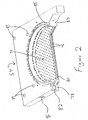
- FIG 3 shows an embodiment of the invention, in which the baffle plate takes the form of the baffle plate assembly 154, which is designed for incorporation into a 300 millimeter (mm) wafer processing system.
- Figure 3 is a partial cutaway, perspective view of a 300 mm photoresist asher chamber assembly 100 (shown without an associated radiant heater assembly) into which is incorporated this baffle plate assembly 154.
- the baffle plate assembly 154 comprises a generally planar upper baffle plate 155 and lower baffle plate 157 positioned generally parallel to each other and separated from one another.
- the assembly 154 is shown attached to the 300 mm process chamber 116.
- the upper and lower baffle plates 155 and 157, respectively, are provided with apertures 175 and 176.
- the apertures 175 in the upper baffle plate are slightly larger than the apertures 176 in the lower baffle plate.
- a process chamber access port 128 is provided for either a vacuum pump or a monochromator.
- both the baffle plate assembly 154 and the process chamber 116 may be provided with active cooling mechanisms.
- internal cooling channels 156 are provided in the side walls 153 thereof. Cooling medium inlets 158 and 160, respectively, are provided to permit entry and exit of a cooling medium, such as water, and out of the cooling channels.
- the process chamber side walls 153 are preferably formed from low-alloy anodized aluminum (e.g. , Alcoa type C-276), which permits the cooling passages 156 to be drilled or machined directly therein, thereby making the side walls less sensitive to inconsistencies in the reflector heating system, and allowing for operation at a substantially uniform process temperature.
- the upper baffle plate 155 is comprised merely of a solid, apertured quartz plate, attached to the lower plate by means of posts 161 at attachment points 159 (see Figure 4 and 6 ).
- the upper baffle plate which may be sapphire coated, functions to divert a portion of the hot gaseous plasma which does not pass through its apertures 175 radially outward, so as to prevent the radially inward potion of the wafer 18 being processed from overheating and to promote reaction rate uniformity.
- a non-apertured sapphire plate 177 covers the central portion of the upper baffle plate 155.
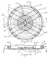
- the active cooling mechanism provided by the lower baffle plate 157 is more clearly shown in its partial cutaway, perspective view in Figure 4 .
- the lower baffle plate 157 comprises a generally planar gas distribution central portion 174, having the apertures 176 therein, surrounded by a flange 178.
- the flange 178 provides the surface to which a top wall 181 of the process chamber 116 may be attached using mounting holes 184.
- Seal 179 provides an airtight connection between the flange 178 and the side wall 153 ( Figure 3 ).
- the seal 179 resides in a groove 183 in flange 178 ( Figure 4 ).
- the central apertured portion 174 of the baffle plate 157 is provided with internal cooling passages 180 connected to cooling medium inlet 182 and outlet 186 ( Figure 3 ). As shown in Figures 4 and 6 , the cooling passages 180 may extend from the flange 178 into and about the central portion 174 in a configuration that avoids intersection with any of the apertures 176. One preferred configuration is shown in Figure 7 .
- cooling channels may also extend into the process chamber top wall.
- These individual cooling subsystems of these structural components i.e., baffle plate, side walls and top wall
- the cooling subsystems may either share a single gas or liquid coolant circulating system, or may be provided with independent circulating systems (gas or liquid) so as to provide independent temperature control and individual flow control thereof.
- active cooling of the process chamber side walls and top wall by maintaining these chamber surfaces at between 15° C - 30° C (just above the dew point), the wafer can remain sufficiently cool to prevent photoresist cracking during, for example, high-density ion implanted (HDII) wafer ash processes.
- HDII high-density ion implanted
- the cooling passages minimize the spatial temperature gradient across the surface of the lower baffle plate 157 and maintain the entire surface of the baffle plate at a uniform temperature.
- the cooling medium such as water (maintained, e.g., at 15° C - 80° C) flows into the channels 180 via inlets 182 and flows out via outlets 186 ( Figures 5 and 7 ), using a deionized water recirculating system including an air-cooled chiller assembly.
- the chiller assembly has a heat removal capacity greater than the heat generation rate of the process chamber even during rapid heating of the wafer.
- the lower baffle plate can be operated at up to 250° C to remove process residues from the surface of the plate. These residues may otherwise condense and remain on the surface of the lower plate if not periodically exposed to higher temperatures during wafer processing.
- the lower baffle plate 157 functions as a heat exchanger to remove heat from the reactive gases, thereby reducing their temperature.
- the lower baffle plate 157 is preferably formed from a single piece of low-alloy anodized aluminum (e.g. , Alcoa type C-276), which improves the heat transfer characteristics of the baffle plate over known quartz baffle plates.
- low-alloy anodized aluminum e.g. , Alcoa type C-276
- the use of aluminum also permits the cooling passages to be drilled or machined directly therein. This makes the baffle plate less sensitive to inconsistencies in the reflector heating system and parasitic heating from the wafer, and allows for operation at a substantially uniform temperature.
- a pressure drop across the lower baffle plate 157 distributes the gas flow across the upper surface of the plate, in addition to increasing the heat transfer rate between the gas and the plate surfaces.
- This same effect in combination with the upper quartz plate 155, reduces mobile ion contamination that can potentially cause device damage such as compromising the dielectric strength of gate oxides.
- the combination of the quartz upper plate 155 and the aluminium lower plate 157 in the dual-layered baffle plate assembly 154 has been found to be suitable for use in the corrosive conditions found in a process chamber used for photoresist removal, even when corrosive element-producing gases such as CF 4 are utilized.
- the systems 10 (200 mm) and 100 (300 mm) have been operated using the water-cooled baffle plate 157 and the baffle plate assembly 154, respectively, at maximum microwave power, under which conditions the gas temperatures have been reduced below the minimum expected process temperature, typically 80°C. Also, it has been possible to obtain a relatively flat temperature profile across the surface of the wafer during processing, resulting in reduced process non-uniformity due to the gas and radiation cooling effects of the cooled lower baffle plate. Active cooling of the lower baffle plate also reduces thermal loading of the baffle plate by the first-processed wafer to improve wafer-to-wafer process uniformity.
- a 270°C ashing process was run while flowing water at 30° C through the lower baffle plate 157 at a flow rate of 1.5 litres per minute (.4 gallon per minute (gpm)).
- An ash rate of 5.59 microns per minute was achieved with a 2.25% ash rate non-uniformity across the wafer.
- An ash rate of 5.66 microns per minute with a 6.2% ash rate non-uniformity across the wafer was obtained with a prior quartz non-actively cooled baffle plate.
Claims (9)
- Gasverteilungsplatte (154) für ein Plasmaverarbeitungssystem, umfassend:(i) einen im Allgemeinen ebenen Mittenbereich (174) mit Öffnungen (176) darin, um Gas zu erlauben, dort hindurchzugehen;(ii) den im Allgemeinen ebenen Mittenbereich (174), der interne Kühlmitteldurchgänge (180) umfasst, die mit einem Kühlmitteleinlass (182) und einem Kühlmittelauslass (186) verbunden sind, wobei die Kühlmitteldurchgänge betreibbar sind, um den Kreislauf eines Kühlmittels dort hindurch zu erlauben, und somit betreibbar ist, um die Betriebstemperatur der Gasverteilungsplatte (154) zu reduzieren, wobei sich die Kühlmitteldurchgänge (180) auf den im Allgemeinen ebenen Mittenbereich (174) in einer Konfiguration erstrecken, die eine Überschneidung mit den Öffnungen (176) vermeidet:(iii) eine im Allgemeinen ebene, obere Ablenkplatte (155), die an der Gasverteilungsplatte (154) befestigt und von ihr beabstandet ist, wobei die obere Ablenkplatte mit Öffnungen (175) versehen ist; und(iv) eine ungelochte Saphirplatte (177), die den Mittenbereich der oberen Ablenkplatte (155) abdeckt.
- Gasverteilungsplatte (154) nach Anspruch 1, wobei der Mittenbereich (174) von einem Flansch (178) umgeben ist, wobei sich die Kühlmitteldurchgänge (180) von dem Flansch aus in den gelochten Mittenbereich erstrecken.
- Gasverteilungsplatte (154) nach Anspruch 1, wobei die Gasverteilungsplatte (154) aus niedrig legiertem, eloxiertem Aluminium besteht und die Kühlmitteldurchgänge (180) darin eingearbeitet sind.
- Verfahren zur Verwendung der Gasverteilungsplatte (154) nach Anspruch (1) umfassend das Zirkulieren eines Flüssigkühlmittels durch die Kühlmitteldurchgänge (180).
- Verfahren nach Anspruch 4, wobei das Kühlmittel Wasser ist.
- Verfahren zur Verwendung der Gasverteilungsplatte (154) nach Anspruch (1) umfassend das Zirkulieren eines Gaskühlmittels durch die Kühlmitteldurchgänge (180).
- Verfahren nach Anspruch 6, wobei das Kühlmittel Helium oder Stickstoff ist.
- Gasverteilungsplatte (154) nach Anspruch 1, wobei die Öffnungen (175) in der oberen Ablenkplatte (155) etwas größer als die Öffnungen (176) in der unteren Ablenkplatte (157) sind.
- Gasverteilungsplatte (154) nach Anspruch 1, wobei die obere Ablenkplatte (155) aus Quarz besteht.
Applications Claiming Priority (2)
| Application Number | Priority Date | Filing Date | Title |
|---|---|---|---|
| US09/560,538 US6635117B1 (en) | 2000-04-26 | 2000-04-26 | Actively-cooled distribution plate for reducing reactive gas temperature in a plasma processing system |
| EP01303757A EP1150330B1 (de) | 2000-04-26 | 2001-04-25 | Aktiv gekühlte Verteilungsplatte zur Temperaturreduzierung der reaktiven Gase in einem Plasmabehandlungssystem |
Related Parent Applications (2)
| Application Number | Title | Priority Date | Filing Date |
|---|---|---|---|
| EP01303757.7 Division | 2001-04-25 | ||
| EP01303757A Division EP1150330B1 (de) | 2000-04-26 | 2001-04-25 | Aktiv gekühlte Verteilungsplatte zur Temperaturreduzierung der reaktiven Gase in einem Plasmabehandlungssystem |
Publications (3)
| Publication Number | Publication Date |
|---|---|
| EP1770753A2 EP1770753A2 (de) | 2007-04-04 |
| EP1770753A3 EP1770753A3 (de) | 2008-02-20 |
| EP1770753B1 true EP1770753B1 (de) | 2010-12-22 |
Family
ID=24238217
Family Applications (2)
| Application Number | Title | Priority Date | Filing Date |
|---|---|---|---|
| EP01303757A Expired - Lifetime EP1150330B1 (de) | 2000-04-26 | 2001-04-25 | Aktiv gekühlte Verteilungsplatte zur Temperaturreduzierung der reaktiven Gase in einem Plasmabehandlungssystem |
| EP06022819A Expired - Lifetime EP1770753B1 (de) | 2000-04-26 | 2001-04-25 | Aktiv gekühlte Verteilungsplatte zur Temperaturreduzierung der reaktiven Gase in einem Plasmabehandlungssystem |
Family Applications Before (1)
| Application Number | Title | Priority Date | Filing Date |
|---|---|---|---|
| EP01303757A Expired - Lifetime EP1150330B1 (de) | 2000-04-26 | 2001-04-25 | Aktiv gekühlte Verteilungsplatte zur Temperaturreduzierung der reaktiven Gase in einem Plasmabehandlungssystem |
Country Status (6)
| Country | Link |
|---|---|
| US (2) | US6635117B1 (de) |
| EP (2) | EP1150330B1 (de) |
| JP (1) | JP4793528B2 (de) |
| KR (1) | KR100587628B1 (de) |
| DE (2) | DE60143717D1 (de) |
| TW (1) | TW490705B (de) |
Cited By (2)
| Publication number | Priority date | Publication date | Assignee | Title |
|---|---|---|---|---|
| US8916793B2 (en) | 2010-06-08 | 2014-12-23 | Applied Materials, Inc. | Temperature control in plasma processing apparatus using pulsed heat transfer fluid flow |
| US9338871B2 (en) | 2010-01-29 | 2016-05-10 | Applied Materials, Inc. | Feedforward temperature control for plasma processing apparatus |
Families Citing this family (416)
| Publication number | Priority date | Publication date | Assignee | Title |
|---|---|---|---|---|
| US6635117B1 (en) * | 2000-04-26 | 2003-10-21 | Axcelis Technologies, Inc. | Actively-cooled distribution plate for reducing reactive gas temperature in a plasma processing system |
| US6537419B1 (en) * | 2000-04-26 | 2003-03-25 | David W. Kinnard | Gas distribution plate assembly for providing laminar gas flow across the surface of a substrate |
| US6939434B2 (en) * | 2000-08-11 | 2005-09-06 | Applied Materials, Inc. | Externally excited torroidal plasma source with magnetic control of ion distribution |
| JP2002129334A (ja) * | 2000-10-26 | 2002-05-09 | Applied Materials Inc | 気相堆積装置のクリーニング方法及び気相堆積装置 |
| KR100434487B1 (ko) * | 2001-01-17 | 2004-06-05 | 삼성전자주식회사 | 샤워 헤드 및 이를 포함하는 박막 형성 장비 |
| DE10134513A1 (de) * | 2001-07-16 | 2003-01-30 | Unaxis Balzers Ag | Hebe-und Stützvorichtung |
| KR100476370B1 (ko) * | 2002-07-19 | 2005-03-16 | 주식회사 하이닉스반도체 | 배치형 원자층증착장치 및 그의 인시튜 세정 방법 |
| US6945054B1 (en) | 2002-10-04 | 2005-09-20 | Richard S. Norman | Method and apparatus for cooling microelectronic complexes including multiple discrete functional modules |
| US8580076B2 (en) * | 2003-05-22 | 2013-11-12 | Lam Research Corporation | Plasma apparatus, gas distribution assembly for a plasma apparatus and processes therewith |
| US20040235299A1 (en) * | 2003-05-22 | 2004-11-25 | Axcelis Technologies, Inc. | Plasma ashing apparatus and endpoint detection process |
| US6976782B1 (en) | 2003-11-24 | 2005-12-20 | Lam Research Corporation | Methods and apparatus for in situ substrate temperature monitoring |
| US7892357B2 (en) * | 2004-01-12 | 2011-02-22 | Axcelis Technologies, Inc. | Gas distribution plate assembly for plasma reactors |
| US20050221618A1 (en) * | 2004-03-31 | 2005-10-06 | Amrhein Frederick J | System for controlling a plenum output flow geometry |
| US20050241767A1 (en) * | 2004-04-30 | 2005-11-03 | Ferris David S | Multi-piece baffle plate assembly for a plasma processing system |
| US20050250346A1 (en) * | 2004-05-06 | 2005-11-10 | Applied Materials, Inc. | Process and apparatus for post deposition treatment of low k dielectric materials |
| US7988816B2 (en) | 2004-06-21 | 2011-08-02 | Tokyo Electron Limited | Plasma processing apparatus and method |
| US7951262B2 (en) | 2004-06-21 | 2011-05-31 | Tokyo Electron Limited | Plasma processing apparatus and method |
| US20050284573A1 (en) * | 2004-06-24 | 2005-12-29 | Egley Fred D | Bare aluminum baffles for resist stripping chambers |
| US20060000802A1 (en) * | 2004-06-30 | 2006-01-05 | Ajay Kumar | Method and apparatus for photomask plasma etching |
| US8349128B2 (en) * | 2004-06-30 | 2013-01-08 | Applied Materials, Inc. | Method and apparatus for stable plasma processing |
| US20060021574A1 (en) * | 2004-08-02 | 2006-02-02 | Veeco Instruments Inc. | Multi-gas distribution injector for chemical vapor deposition reactors |
| WO2006026765A2 (en) * | 2004-09-01 | 2006-03-09 | Axcelis Technologies, Inc. | Plasma ashing process for increasing photoresist removal rate and plasma apparatus wuth cooling means |
| JP2006080347A (ja) * | 2004-09-10 | 2006-03-23 | Hitachi High-Technologies Corp | プラズマ処理装置 |
| US20060228889A1 (en) * | 2005-03-31 | 2006-10-12 | Edelberg Erik A | Methods of removing resist from substrates in resist stripping chambers |
| US8298336B2 (en) * | 2005-04-01 | 2012-10-30 | Lam Research Corporation | High strip rate downstream chamber |
| US20060249175A1 (en) * | 2005-05-09 | 2006-11-09 | Applied Materials, Inc. | High efficiency UV curing system |
| US20060251827A1 (en) * | 2005-05-09 | 2006-11-09 | Applied Materials, Inc. | Tandem uv chamber for curing dielectric materials |
| JP4664119B2 (ja) | 2005-05-17 | 2011-04-06 | 東京エレクトロン株式会社 | プラズマ処理装置 |
| JP5044931B2 (ja) * | 2005-10-31 | 2012-10-10 | 東京エレクトロン株式会社 | ガス供給装置及び基板処理装置 |
| TWI329135B (en) * | 2005-11-04 | 2010-08-21 | Applied Materials Inc | Apparatus and process for plasma-enhanced atomic layer deposition |
| KR100738873B1 (ko) | 2006-02-07 | 2007-07-12 | 주식회사 에스에프에이 | 평면디스플레이용 화학 기상 증착장치 |
| US7476291B2 (en) * | 2006-09-28 | 2009-01-13 | Lam Research Corporation | High chamber temperature process and chamber design for photo-resist stripping and post-metal etch passivation |
| US7943005B2 (en) * | 2006-10-30 | 2011-05-17 | Applied Materials, Inc. | Method and apparatus for photomask plasma etching |
| US7909961B2 (en) * | 2006-10-30 | 2011-03-22 | Applied Materials, Inc. | Method and apparatus for photomask plasma etching |
| KR100766440B1 (ko) * | 2006-12-22 | 2007-10-15 | 엘지전자 주식회사 | 전자레인지의 히터장치 |
| WO2008114363A1 (ja) * | 2007-03-16 | 2008-09-25 | Fujitsu Microelectronics Limited | 半導体装置の製造装置、および半導体装置の製造方法 |
| JP2008243937A (ja) | 2007-03-26 | 2008-10-09 | Tokyo Electron Ltd | 基板処理装置及び基板処理方法 |
| US8500382B2 (en) * | 2007-05-22 | 2013-08-06 | Axcelis Technologies Inc. | Airflow management for particle abatement in semiconductor manufacturing equipment |
| US7651269B2 (en) * | 2007-07-19 | 2010-01-26 | Lam Research Corporation | Temperature probes having a thermally isolated tip |
| US8673080B2 (en) | 2007-10-16 | 2014-03-18 | Novellus Systems, Inc. | Temperature controlled showerhead |
| JP5230225B2 (ja) * | 2008-03-06 | 2013-07-10 | 東京エレクトロン株式会社 | 蓋部品、処理ガス拡散供給装置、及び基板処理装置 |
| US8252114B2 (en) * | 2008-03-28 | 2012-08-28 | Tokyo Electron Limited | Gas distribution system and method for distributing process gas in a processing system |
| US20100206229A1 (en) * | 2008-05-30 | 2010-08-19 | Alta Devices, Inc. | Vapor deposition reactor system |
| US20100212591A1 (en) * | 2008-05-30 | 2010-08-26 | Alta Devices, Inc. | Reactor lid assembly for vapor deposition |
| US8679288B2 (en) | 2008-06-09 | 2014-03-25 | Lam Research Corporation | Showerhead electrode assemblies for plasma processing apparatuses |
| KR101606736B1 (ko) | 2008-07-07 | 2016-03-28 | 램 리써치 코포레이션 | 플라즈마 프로세싱 챔버에서 플라즈마 불안정성을 검출하기 위한 패시브 용량성-결합된 정전식 (cce) 프로브 장치 |
| TWI494030B (zh) * | 2008-07-07 | 2015-07-21 | Lam Res Corp | 供使用於電漿處理腔室中之含真空間隙的面向電漿之探針裝置 |
| JP5231117B2 (ja) * | 2008-07-24 | 2013-07-10 | 株式会社ニューフレアテクノロジー | 成膜装置および成膜方法 |
| EP2151509A1 (de) * | 2008-08-04 | 2010-02-10 | Applied Materials, Inc. | Verteiler für reaktives Gas, Behandlungssystem für reaktives Gas und Behandlungsverfahren für reaktives Gas |
| US8449679B2 (en) | 2008-08-15 | 2013-05-28 | Lam Research Corporation | Temperature controlled hot edge ring assembly |
| US10378106B2 (en) | 2008-11-14 | 2019-08-13 | Asm Ip Holding B.V. | Method of forming insulation film by modified PEALD |
| KR101037188B1 (ko) | 2008-12-17 | 2011-05-26 | 세메스 주식회사 | 플라즈마 처리 장치 |
| JP5479867B2 (ja) | 2009-01-14 | 2014-04-23 | 東京エレクトロン株式会社 | 誘導結合プラズマ処理装置 |
| CN102422393A (zh) * | 2009-03-16 | 2012-04-18 | 奥塔装置公司 | 用于气相沉积的淋喷头 |
| US9394608B2 (en) | 2009-04-06 | 2016-07-19 | Asm America, Inc. | Semiconductor processing reactor and components thereof |
| KR101110080B1 (ko) * | 2009-07-08 | 2012-03-13 | 주식회사 유진테크 | 확산판을 선택적으로 삽입설치하는 기판처리방법 |
| US8802201B2 (en) | 2009-08-14 | 2014-08-12 | Asm America, Inc. | Systems and methods for thin-film deposition of metal oxides using excited nitrogen-oxygen species |
| KR101796656B1 (ko) | 2010-04-30 | 2017-11-13 | 어플라이드 머티어리얼스, 인코포레이티드 | 수직 인라인 화학기상증착 시스템 |
| US8880227B2 (en) * | 2010-05-27 | 2014-11-04 | Applied Materials, Inc. | Component temperature control by coolant flow control and heater duty cycle control |
| JP5373702B2 (ja) * | 2010-06-07 | 2013-12-18 | 株式会社Sen | イオンビームスキャン処理装置及びイオンビームスキャン処理方法 |
| US8845806B2 (en) * | 2010-10-22 | 2014-09-30 | Asm Japan K.K. | Shower plate having different aperture dimensions and/or distributions |
| US9105705B2 (en) * | 2011-03-14 | 2015-08-11 | Plasma-Therm Llc | Method and apparatus for plasma dicing a semi-conductor wafer |
| US9129778B2 (en) | 2011-03-18 | 2015-09-08 | Lam Research Corporation | Fluid distribution members and/or assemblies |
| US9245717B2 (en) | 2011-05-31 | 2016-01-26 | Lam Research Corporation | Gas distribution system for ceramic showerhead of plasma etch reactor |
| US8562785B2 (en) * | 2011-05-31 | 2013-10-22 | Lam Research Corporation | Gas distribution showerhead for inductively coupled plasma etch reactor |
| US9312155B2 (en) | 2011-06-06 | 2016-04-12 | Asm Japan K.K. | High-throughput semiconductor-processing apparatus equipped with multiple dual-chamber modules |
| US20120315396A1 (en) * | 2011-06-13 | 2012-12-13 | Intermolecular, Inc. | Apparatus and method for combinatorial plasma distribution through a multi-zoned showerhead |
| US9793148B2 (en) | 2011-06-22 | 2017-10-17 | Asm Japan K.K. | Method for positioning wafers in multiple wafer transport |
| US10364496B2 (en) | 2011-06-27 | 2019-07-30 | Asm Ip Holding B.V. | Dual section module having shared and unshared mass flow controllers |
| US10854498B2 (en) | 2011-07-15 | 2020-12-01 | Asm Ip Holding B.V. | Wafer-supporting device and method for producing same |
| US20130023129A1 (en) | 2011-07-20 | 2013-01-24 | Asm America, Inc. | Pressure transmitter for a semiconductor processing environment |
| US10274270B2 (en) | 2011-10-27 | 2019-04-30 | Applied Materials, Inc. | Dual zone common catch heat exchanger/chiller |
| US9017481B1 (en) | 2011-10-28 | 2015-04-28 | Asm America, Inc. | Process feed management for semiconductor substrate processing |
| US8946830B2 (en) | 2012-04-04 | 2015-02-03 | Asm Ip Holdings B.V. | Metal oxide protective layer for a semiconductor device |
| US9447499B2 (en) | 2012-06-22 | 2016-09-20 | Novellus Systems, Inc. | Dual plenum, axi-symmetric showerhead with edge-to-center gas delivery |
| US8875728B2 (en) * | 2012-07-12 | 2014-11-04 | Siliken Chemicals, S.L. | Cooled gas distribution plate, thermal bridge breaking system, and related methods |
| US9558931B2 (en) | 2012-07-27 | 2017-01-31 | Asm Ip Holding B.V. | System and method for gas-phase sulfur passivation of a semiconductor surface |
| JP6172660B2 (ja) * | 2012-08-23 | 2017-08-02 | 東京エレクトロン株式会社 | 成膜装置、及び、低誘電率膜を形成する方法 |
| US9659799B2 (en) | 2012-08-28 | 2017-05-23 | Asm Ip Holding B.V. | Systems and methods for dynamic semiconductor process scheduling |
| US9021985B2 (en) | 2012-09-12 | 2015-05-05 | Asm Ip Holdings B.V. | Process gas management for an inductively-coupled plasma deposition reactor |
| KR20140038070A (ko) * | 2012-09-20 | 2014-03-28 | 삼성코닝정밀소재 주식회사 | 가스 분사 장치 및 이에 사용되는 인젝터 파이프 |
| US9324811B2 (en) | 2012-09-26 | 2016-04-26 | Asm Ip Holding B.V. | Structures and devices including a tensile-stressed silicon arsenic layer and methods of forming same |
| US10714315B2 (en) | 2012-10-12 | 2020-07-14 | Asm Ip Holdings B.V. | Semiconductor reaction chamber showerhead |
| JP6096470B2 (ja) * | 2012-10-29 | 2017-03-15 | 東京エレクトロン株式会社 | プラズマ処理方法及びプラズマ処理装置 |
| US10316409B2 (en) * | 2012-12-21 | 2019-06-11 | Novellus Systems, Inc. | Radical source design for remote plasma atomic layer deposition |
| US9640416B2 (en) | 2012-12-26 | 2017-05-02 | Asm Ip Holding B.V. | Single-and dual-chamber module-attachable wafer-handling chamber |
| US20140235069A1 (en) * | 2013-02-15 | 2014-08-21 | Novellus Systems, Inc. | Multi-plenum showerhead with temperature control |
| US9748121B2 (en) * | 2013-03-05 | 2017-08-29 | Applied Materials, Inc. | Thermal coupled quartz dome heat sink |
| US9484191B2 (en) | 2013-03-08 | 2016-11-01 | Asm Ip Holding B.V. | Pulsed remote plasma method and system |
| US9589770B2 (en) | 2013-03-08 | 2017-03-07 | Asm Ip Holding B.V. | Method and systems for in-situ formation of intermediate reactive species |
| US9322097B2 (en) | 2013-03-13 | 2016-04-26 | Applied Materials, Inc. | EPI base ring |
| CN103276371B (zh) * | 2013-03-26 | 2015-12-09 | 中晟光电设备(上海)有限公司 | Cvd设备的进气装置、冷却装置及冷却方法 |
| US9677176B2 (en) | 2013-07-03 | 2017-06-13 | Novellus Systems, Inc. | Multi-plenum, dual-temperature showerhead |
| US8993054B2 (en) | 2013-07-12 | 2015-03-31 | Asm Ip Holding B.V. | Method and system to reduce outgassing in a reaction chamber |
| US9859145B2 (en) * | 2013-07-17 | 2018-01-02 | Lam Research Corporation | Cooled pin lifter paddle for semiconductor substrate processing apparatus |
| US9018111B2 (en) | 2013-07-22 | 2015-04-28 | Asm Ip Holding B.V. | Semiconductor reaction chamber with plasma capabilities |
| US9793115B2 (en) | 2013-08-14 | 2017-10-17 | Asm Ip Holding B.V. | Structures and devices including germanium-tin films and methods of forming same |
| US9240412B2 (en) | 2013-09-27 | 2016-01-19 | Asm Ip Holding B.V. | Semiconductor structure and device and methods of forming same using selective epitaxial process |
| US9556516B2 (en) | 2013-10-09 | 2017-01-31 | ASM IP Holding B.V | Method for forming Ti-containing film by PEALD using TDMAT or TDEAT |
| US10179947B2 (en) | 2013-11-26 | 2019-01-15 | Asm Ip Holding B.V. | Method for forming conformal nitrided, oxidized, or carbonized dielectric film by atomic layer deposition |
| US10683571B2 (en) | 2014-02-25 | 2020-06-16 | Asm Ip Holding B.V. | Gas supply manifold and method of supplying gases to chamber using same |
| US9447498B2 (en) | 2014-03-18 | 2016-09-20 | Asm Ip Holding B.V. | Method for performing uniform processing in gas system-sharing multiple reaction chambers |
| US10167557B2 (en) | 2014-03-18 | 2019-01-01 | Asm Ip Holding B.V. | Gas distribution system, reactor including the system, and methods of using the same |
| US11015245B2 (en) | 2014-03-19 | 2021-05-25 | Asm Ip Holding B.V. | Gas-phase reactor and system having exhaust plenum and components thereof |
| US9404587B2 (en) | 2014-04-24 | 2016-08-02 | ASM IP Holding B.V | Lockout tagout for semiconductor vacuum valve |
| US10741365B2 (en) | 2014-05-05 | 2020-08-11 | Lam Research Corporation | Low volume showerhead with porous baffle |
| US10858737B2 (en) | 2014-07-28 | 2020-12-08 | Asm Ip Holding B.V. | Showerhead assembly and components thereof |
| US9543180B2 (en) | 2014-08-01 | 2017-01-10 | Asm Ip Holding B.V. | Apparatus and method for transporting wafers between wafer carrier and process tool under vacuum |
| US9890456B2 (en) | 2014-08-21 | 2018-02-13 | Asm Ip Holding B.V. | Method and system for in situ formation of gas-phase compounds |
| KR101568363B1 (ko) | 2014-08-27 | 2015-11-12 | 피에스케이 주식회사 | 기판 처리 장치 및 배플 |
| US9657845B2 (en) | 2014-10-07 | 2017-05-23 | Asm Ip Holding B.V. | Variable conductance gas distribution apparatus and method |
| US10941490B2 (en) | 2014-10-07 | 2021-03-09 | Asm Ip Holding B.V. | Multiple temperature range susceptor, assembly, reactor and system including the susceptor, and methods of using the same |
| KR102300403B1 (ko) | 2014-11-19 | 2021-09-09 | 에이에스엠 아이피 홀딩 비.브이. | 박막 증착 방법 |
| KR102263121B1 (ko) | 2014-12-22 | 2021-06-09 | 에이에스엠 아이피 홀딩 비.브이. | 반도체 소자 및 그 제조 방법 |
| US9478415B2 (en) | 2015-02-13 | 2016-10-25 | Asm Ip Holding B.V. | Method for forming film having low resistance and shallow junction depth |
| US10529542B2 (en) | 2015-03-11 | 2020-01-07 | Asm Ip Holdings B.V. | Cross-flow reactor and method |
| US10276355B2 (en) | 2015-03-12 | 2019-04-30 | Asm Ip Holding B.V. | Multi-zone reactor, system including the reactor, and method of using the same |
| US10378107B2 (en) * | 2015-05-22 | 2019-08-13 | Lam Research Corporation | Low volume showerhead with faceplate holes for improved flow uniformity |
| US10023959B2 (en) | 2015-05-26 | 2018-07-17 | Lam Research Corporation | Anti-transient showerhead |
| US10458018B2 (en) | 2015-06-26 | 2019-10-29 | Asm Ip Holding B.V. | Structures including metal carbide material, devices including the structures, and methods of forming same |
| US10600673B2 (en) | 2015-07-07 | 2020-03-24 | Asm Ip Holding B.V. | Magnetic susceptor to baseplate seal |
| US9899291B2 (en) | 2015-07-13 | 2018-02-20 | Asm Ip Holding B.V. | Method for protecting layer by forming hydrocarbon-based extremely thin film |
| US10043661B2 (en) | 2015-07-13 | 2018-08-07 | Asm Ip Holding B.V. | Method for protecting layer by forming hydrocarbon-based extremely thin film |
| CN106356318B (zh) * | 2015-07-16 | 2019-10-18 | 中微半导体设备(上海)股份有限公司 | 一种气体分布扩散板、等离子体处理器 |
| US10083836B2 (en) | 2015-07-24 | 2018-09-25 | Asm Ip Holding B.V. | Formation of boron-doped titanium metal films with high work function |
| US10087525B2 (en) | 2015-08-04 | 2018-10-02 | Asm Ip Holding B.V. | Variable gap hard stop design |
| US9647114B2 (en) | 2015-08-14 | 2017-05-09 | Asm Ip Holding B.V. | Methods of forming highly p-type doped germanium tin films and structures and devices including the films |
| US9711345B2 (en) | 2015-08-25 | 2017-07-18 | Asm Ip Holding B.V. | Method for forming aluminum nitride-based film by PEALD |
| US9960072B2 (en) | 2015-09-29 | 2018-05-01 | Asm Ip Holding B.V. | Variable adjustment for precise matching of multiple chamber cavity housings |
| US9909214B2 (en) | 2015-10-15 | 2018-03-06 | Asm Ip Holding B.V. | Method for depositing dielectric film in trenches by PEALD |
| US9899210B2 (en) | 2015-10-20 | 2018-02-20 | Taiwan Semiconductor Manufacturing Co., Ltd. | Chemical vapor deposition apparatus and method for manufacturing semiconductor device using the same |
| US10211308B2 (en) | 2015-10-21 | 2019-02-19 | Asm Ip Holding B.V. | NbMC layers |
| US10322384B2 (en) | 2015-11-09 | 2019-06-18 | Asm Ip Holding B.V. | Counter flow mixer for process chamber |
| US9455138B1 (en) | 2015-11-10 | 2016-09-27 | Asm Ip Holding B.V. | Method for forming dielectric film in trenches by PEALD using H-containing gas |
| US9905420B2 (en) | 2015-12-01 | 2018-02-27 | Asm Ip Holding B.V. | Methods of forming silicon germanium tin films and structures and devices including the films |
| US9607837B1 (en) | 2015-12-21 | 2017-03-28 | Asm Ip Holding B.V. | Method for forming silicon oxide cap layer for solid state diffusion process |
| US9627221B1 (en) | 2015-12-28 | 2017-04-18 | Asm Ip Holding B.V. | Continuous process incorporating atomic layer etching |
| US9735024B2 (en) | 2015-12-28 | 2017-08-15 | Asm Ip Holding B.V. | Method of atomic layer etching using functional group-containing fluorocarbon |
| US11139308B2 (en) | 2015-12-29 | 2021-10-05 | Asm Ip Holding B.V. | Atomic layer deposition of III-V compounds to form V-NAND devices |
| US9754779B1 (en) | 2016-02-19 | 2017-09-05 | Asm Ip Holding B.V. | Method for forming silicon nitride film selectively on sidewalls or flat surfaces of trenches |
| US10529554B2 (en) | 2016-02-19 | 2020-01-07 | Asm Ip Holding B.V. | Method for forming silicon nitride film selectively on sidewalls or flat surfaces of trenches |
| US10468251B2 (en) | 2016-02-19 | 2019-11-05 | Asm Ip Holding B.V. | Method for forming spacers using silicon nitride film for spacer-defined multiple patterning |
| US10501866B2 (en) | 2016-03-09 | 2019-12-10 | Asm Ip Holding B.V. | Gas distribution apparatus for improved film uniformity in an epitaxial system |
| US10343920B2 (en) | 2016-03-18 | 2019-07-09 | Asm Ip Holding B.V. | Aligned carbon nanotubes |
| US9892913B2 (en) | 2016-03-24 | 2018-02-13 | Asm Ip Holding B.V. | Radial and thickness control via biased multi-port injection settings |
| US10865475B2 (en) | 2016-04-21 | 2020-12-15 | Asm Ip Holding B.V. | Deposition of metal borides and silicides |
| US10190213B2 (en) | 2016-04-21 | 2019-01-29 | Asm Ip Holding B.V. | Deposition of metal borides |
| US10087522B2 (en) | 2016-04-21 | 2018-10-02 | Asm Ip Holding B.V. | Deposition of metal borides |
| US10367080B2 (en) | 2016-05-02 | 2019-07-30 | Asm Ip Holding B.V. | Method of forming a germanium oxynitride film |
| US10032628B2 (en) | 2016-05-02 | 2018-07-24 | Asm Ip Holding B.V. | Source/drain performance through conformal solid state doping |
| KR102592471B1 (ko) | 2016-05-17 | 2023-10-20 | 에이에스엠 아이피 홀딩 비.브이. | 금속 배선 형성 방법 및 이를 이용한 반도체 장치의 제조 방법 |
| US11453943B2 (en) | 2016-05-25 | 2022-09-27 | Asm Ip Holding B.V. | Method for forming carbon-containing silicon/metal oxide or nitride film by ALD using silicon precursor and hydrocarbon precursor |
| US10388509B2 (en) | 2016-06-28 | 2019-08-20 | Asm Ip Holding B.V. | Formation of epitaxial layers via dislocation filtering |
| US9859151B1 (en) | 2016-07-08 | 2018-01-02 | Asm Ip Holding B.V. | Selective film deposition method to form air gaps |
| US10612137B2 (en) | 2016-07-08 | 2020-04-07 | Asm Ip Holdings B.V. | Organic reactants for atomic layer deposition |
| US9793135B1 (en) | 2016-07-14 | 2017-10-17 | ASM IP Holding B.V | Method of cyclic dry etching using etchant film |
| US10714385B2 (en) | 2016-07-19 | 2020-07-14 | Asm Ip Holding B.V. | Selective deposition of tungsten |
| US10381226B2 (en) | 2016-07-27 | 2019-08-13 | Asm Ip Holding B.V. | Method of processing substrate |
| US10395919B2 (en) | 2016-07-28 | 2019-08-27 | Asm Ip Holding B.V. | Method and apparatus for filling a gap |
| US10177025B2 (en) | 2016-07-28 | 2019-01-08 | Asm Ip Holding B.V. | Method and apparatus for filling a gap |
| US9887082B1 (en) | 2016-07-28 | 2018-02-06 | Asm Ip Holding B.V. | Method and apparatus for filling a gap |
| US9812320B1 (en) | 2016-07-28 | 2017-11-07 | Asm Ip Holding B.V. | Method and apparatus for filling a gap |
| KR102532607B1 (ko) | 2016-07-28 | 2023-05-15 | 에이에스엠 아이피 홀딩 비.브이. | 기판 가공 장치 및 그 동작 방법 |
| US10090316B2 (en) | 2016-09-01 | 2018-10-02 | Asm Ip Holding B.V. | 3D stacked multilayer semiconductor memory using doped select transistor channel |
| US10410943B2 (en) | 2016-10-13 | 2019-09-10 | Asm Ip Holding B.V. | Method for passivating a surface of a semiconductor and related systems |
| US10643826B2 (en) | 2016-10-26 | 2020-05-05 | Asm Ip Holdings B.V. | Methods for thermally calibrating reaction chambers |
| US11532757B2 (en) | 2016-10-27 | 2022-12-20 | Asm Ip Holding B.V. | Deposition of charge trapping layers |
| US10714350B2 (en) | 2016-11-01 | 2020-07-14 | ASM IP Holdings, B.V. | Methods for forming a transition metal niobium nitride film on a substrate by atomic layer deposition and related semiconductor device structures |
| US10643904B2 (en) | 2016-11-01 | 2020-05-05 | Asm Ip Holdings B.V. | Methods for forming a semiconductor device and related semiconductor device structures |
| US10229833B2 (en) | 2016-11-01 | 2019-03-12 | Asm Ip Holding B.V. | Methods for forming a transition metal nitride film on a substrate by atomic layer deposition and related semiconductor device structures |
| US10435790B2 (en) | 2016-11-01 | 2019-10-08 | Asm Ip Holding B.V. | Method of subatmospheric plasma-enhanced ALD using capacitively coupled electrodes with narrow gap |
| US10134757B2 (en) | 2016-11-07 | 2018-11-20 | Asm Ip Holding B.V. | Method of processing a substrate and a device manufactured by using the method |
| KR102546317B1 (ko) | 2016-11-15 | 2023-06-21 | 에이에스엠 아이피 홀딩 비.브이. | 기체 공급 유닛 및 이를 포함하는 기판 처리 장치 |
| US10340135B2 (en) | 2016-11-28 | 2019-07-02 | Asm Ip Holding B.V. | Method of topologically restricted plasma-enhanced cyclic deposition of silicon or metal nitride |
| KR20180068582A (ko) | 2016-12-14 | 2018-06-22 | 에이에스엠 아이피 홀딩 비.브이. | 기판 처리 장치 |
| US10604841B2 (en) | 2016-12-14 | 2020-03-31 | Lam Research Corporation | Integrated showerhead with thermal control for delivering radical and precursor gas to a downstream chamber to enable remote plasma film deposition |
| US11447861B2 (en) | 2016-12-15 | 2022-09-20 | Asm Ip Holding B.V. | Sequential infiltration synthesis apparatus and a method of forming a patterned structure |
| US11581186B2 (en) | 2016-12-15 | 2023-02-14 | Asm Ip Holding B.V. | Sequential infiltration synthesis apparatus |
| US9916980B1 (en) | 2016-12-15 | 2018-03-13 | Asm Ip Holding B.V. | Method of forming a structure on a substrate |
| KR20180070971A (ko) | 2016-12-19 | 2018-06-27 | 에이에스엠 아이피 홀딩 비.브이. | 기판 처리 장치 |
| US10269558B2 (en) | 2016-12-22 | 2019-04-23 | Asm Ip Holding B.V. | Method of forming a structure on a substrate |
| US10867788B2 (en) | 2016-12-28 | 2020-12-15 | Asm Ip Holding B.V. | Method of forming a structure on a substrate |
| US11390950B2 (en) | 2017-01-10 | 2022-07-19 | Asm Ip Holding B.V. | Reactor system and method to reduce residue buildup during a film deposition process |
| US10655221B2 (en) | 2017-02-09 | 2020-05-19 | Asm Ip Holding B.V. | Method for depositing oxide film by thermal ALD and PEALD |
| US10468261B2 (en) | 2017-02-15 | 2019-11-05 | Asm Ip Holding B.V. | Methods for forming a metallic film on a substrate by cyclical deposition and related semiconductor device structures |
| US10529563B2 (en) | 2017-03-29 | 2020-01-07 | Asm Ip Holdings B.V. | Method for forming doped metal oxide films on a substrate by cyclical deposition and related semiconductor device structures |
| US10283353B2 (en) | 2017-03-29 | 2019-05-07 | Asm Ip Holding B.V. | Method of reforming insulating film deposited on substrate with recess pattern |
| US10103040B1 (en) | 2017-03-31 | 2018-10-16 | Asm Ip Holding B.V. | Apparatus and method for manufacturing a semiconductor device |
| USD830981S1 (en) | 2017-04-07 | 2018-10-16 | Asm Ip Holding B.V. | Susceptor for semiconductor substrate processing apparatus |
| KR102457289B1 (ko) | 2017-04-25 | 2022-10-21 | 에이에스엠 아이피 홀딩 비.브이. | 박막 증착 방법 및 반도체 장치의 제조 방법 |
| US10446393B2 (en) | 2017-05-08 | 2019-10-15 | Asm Ip Holding B.V. | Methods for forming silicon-containing epitaxial layers and related semiconductor device structures |
| US10770286B2 (en) | 2017-05-08 | 2020-09-08 | Asm Ip Holdings B.V. | Methods for selectively forming a silicon nitride film on a substrate and related semiconductor device structures |
| US10892156B2 (en) | 2017-05-08 | 2021-01-12 | Asm Ip Holding B.V. | Methods for forming a silicon nitride film on a substrate and related semiconductor device structures |
| US10504742B2 (en) | 2017-05-31 | 2019-12-10 | Asm Ip Holding B.V. | Method of atomic layer etching using hydrogen plasma |
| US10886123B2 (en) | 2017-06-02 | 2021-01-05 | Asm Ip Holding B.V. | Methods for forming low temperature semiconductor layers and related semiconductor device structures |
| US10790119B2 (en) | 2017-06-09 | 2020-09-29 | Mattson Technology, Inc | Plasma processing apparatus with post plasma gas injection |
| US11201036B2 (en) * | 2017-06-09 | 2021-12-14 | Beijing E-Town Semiconductor Technology Co., Ltd | Plasma strip tool with uniformity control |
| US11306395B2 (en) | 2017-06-28 | 2022-04-19 | Asm Ip Holding B.V. | Methods for depositing a transition metal nitride film on a substrate by atomic layer deposition and related deposition apparatus |
| US10685834B2 (en) | 2017-07-05 | 2020-06-16 | Asm Ip Holdings B.V. | Methods for forming a silicon germanium tin layer and related semiconductor device structures |
| KR20190009245A (ko) | 2017-07-18 | 2019-01-28 | 에이에스엠 아이피 홀딩 비.브이. | 반도체 소자 구조물 형성 방법 및 관련된 반도체 소자 구조물 |
| US11374112B2 (en) | 2017-07-19 | 2022-06-28 | Asm Ip Holding B.V. | Method for depositing a group IV semiconductor and related semiconductor device structures |
| US11018002B2 (en) | 2017-07-19 | 2021-05-25 | Asm Ip Holding B.V. | Method for selectively depositing a Group IV semiconductor and related semiconductor device structures |
| US10541333B2 (en) | 2017-07-19 | 2020-01-21 | Asm Ip Holding B.V. | Method for depositing a group IV semiconductor and related semiconductor device structures |
| US10312055B2 (en) | 2017-07-26 | 2019-06-04 | Asm Ip Holding B.V. | Method of depositing film by PEALD using negative bias |
| US10590535B2 (en) | 2017-07-26 | 2020-03-17 | Asm Ip Holdings B.V. | Chemical treatment, deposition and/or infiltration apparatus and method for using the same |
| US10605530B2 (en) | 2017-07-26 | 2020-03-31 | Asm Ip Holding B.V. | Assembly of a liner and a flange for a vertical furnace as well as the liner and the vertical furnace |
| US10692741B2 (en) | 2017-08-08 | 2020-06-23 | Asm Ip Holdings B.V. | Radiation shield |
| US10770336B2 (en) | 2017-08-08 | 2020-09-08 | Asm Ip Holding B.V. | Substrate lift mechanism and reactor including same |
| US11139191B2 (en) | 2017-08-09 | 2021-10-05 | Asm Ip Holding B.V. | Storage apparatus for storing cassettes for substrates and processing apparatus equipped therewith |
| US11769682B2 (en) | 2017-08-09 | 2023-09-26 | Asm Ip Holding B.V. | Storage apparatus for storing cassettes for substrates and processing apparatus equipped therewith |
| US10249524B2 (en) | 2017-08-09 | 2019-04-02 | Asm Ip Holding B.V. | Cassette holder assembly for a substrate cassette and holding member for use in such assembly |
| US10236177B1 (en) | 2017-08-22 | 2019-03-19 | ASM IP Holding B.V.. | Methods for depositing a doped germanium tin semiconductor and related semiconductor device structures |
| USD900036S1 (en) | 2017-08-24 | 2020-10-27 | Asm Ip Holding B.V. | Heater electrical connector and adapter |
| US11830730B2 (en) | 2017-08-29 | 2023-11-28 | Asm Ip Holding B.V. | Layer forming method and apparatus |
| US11295980B2 (en) | 2017-08-30 | 2022-04-05 | Asm Ip Holding B.V. | Methods for depositing a molybdenum metal film over a dielectric surface of a substrate by a cyclical deposition process and related semiconductor device structures |
| KR102491945B1 (ko) | 2017-08-30 | 2023-01-26 | 에이에스엠 아이피 홀딩 비.브이. | 기판 처리 장치 |
| US11056344B2 (en) | 2017-08-30 | 2021-07-06 | Asm Ip Holding B.V. | Layer forming method |
| DE202017105481U1 (de) * | 2017-09-11 | 2018-12-12 | Aixtron Se | Gaseinlassorgan für einen CVD- oder PVD-Reaktor |
| US10607895B2 (en) | 2017-09-18 | 2020-03-31 | Asm Ip Holdings B.V. | Method for forming a semiconductor device structure comprising a gate fill metal |
| KR102630301B1 (ko) | 2017-09-21 | 2024-01-29 | 에이에스엠 아이피 홀딩 비.브이. | 침투성 재료의 순차 침투 합성 방법 처리 및 이를 이용하여 형성된 구조물 및 장치 |
| US10844484B2 (en) | 2017-09-22 | 2020-11-24 | Asm Ip Holding B.V. | Apparatus for dispensing a vapor phase reactant to a reaction chamber and related methods |
| US10658205B2 (en) | 2017-09-28 | 2020-05-19 | Asm Ip Holdings B.V. | Chemical dispensing apparatus and methods for dispensing a chemical to a reaction chamber |
| US10403504B2 (en) | 2017-10-05 | 2019-09-03 | Asm Ip Holding B.V. | Method for selectively depositing a metallic film on a substrate |
| US10319588B2 (en) | 2017-10-10 | 2019-06-11 | Asm Ip Holding B.V. | Method for depositing a metal chalcogenide on a substrate by cyclical deposition |
| US10923344B2 (en) | 2017-10-30 | 2021-02-16 | Asm Ip Holding B.V. | Methods for forming a semiconductor structure and related semiconductor structures |
| KR102443047B1 (ko) | 2017-11-16 | 2022-09-14 | 에이에스엠 아이피 홀딩 비.브이. | 기판 처리 장치 방법 및 그에 의해 제조된 장치 |
| US10910262B2 (en) | 2017-11-16 | 2021-02-02 | Asm Ip Holding B.V. | Method of selectively depositing a capping layer structure on a semiconductor device structure |
| US11022879B2 (en) | 2017-11-24 | 2021-06-01 | Asm Ip Holding B.V. | Method of forming an enhanced unexposed photoresist layer |
| JP7206265B2 (ja) | 2017-11-27 | 2023-01-17 | エーエスエム アイピー ホールディング ビー.ブイ. | クリーン・ミニエンバイロメントを備える装置 |
| CN111316417B (zh) | 2017-11-27 | 2023-12-22 | 阿斯莫Ip控股公司 | 与批式炉偕同使用的用于储存晶圆匣的储存装置 |
| US10290508B1 (en) | 2017-12-05 | 2019-05-14 | Asm Ip Holding B.V. | Method for forming vertical spacers for spacer-defined patterning |
| KR20200087267A (ko) | 2017-12-08 | 2020-07-20 | 램 리써치 코포레이션 | 리모트 플라즈마 막 증착을 인에이블하도록 다운스트림 챔버로 라디칼 및 전구체 가스를 전달하기 위해 개선된 홀 패턴을 갖는 통합된 샤워헤드 |
| US10872771B2 (en) | 2018-01-16 | 2020-12-22 | Asm Ip Holding B. V. | Method for depositing a material film on a substrate within a reaction chamber by a cyclical deposition process and related device structures |
| TW202325889A (zh) | 2018-01-19 | 2023-07-01 | 荷蘭商Asm 智慧財產控股公司 | 沈積方法 |
| CN111630203A (zh) | 2018-01-19 | 2020-09-04 | Asm Ip私人控股有限公司 | 通过等离子体辅助沉积来沉积间隙填充层的方法 |
| USD903477S1 (en) | 2018-01-24 | 2020-12-01 | Asm Ip Holdings B.V. | Metal clamp |
| US11018047B2 (en) | 2018-01-25 | 2021-05-25 | Asm Ip Holding B.V. | Hybrid lift pin |
| US10535516B2 (en) | 2018-02-01 | 2020-01-14 | Asm Ip Holdings B.V. | Method for depositing a semiconductor structure on a surface of a substrate and related semiconductor structures |
| USD880437S1 (en) | 2018-02-01 | 2020-04-07 | Asm Ip Holding B.V. | Gas supply plate for semiconductor manufacturing apparatus |
| US11081345B2 (en) | 2018-02-06 | 2021-08-03 | Asm Ip Holding B.V. | Method of post-deposition treatment for silicon oxide film |
| WO2019158960A1 (en) | 2018-02-14 | 2019-08-22 | Asm Ip Holding B.V. | A method for depositing a ruthenium-containing film on a substrate by a cyclical deposition process |
| US10896820B2 (en) | 2018-02-14 | 2021-01-19 | Asm Ip Holding B.V. | Method for depositing a ruthenium-containing film on a substrate by a cyclical deposition process |
| US10731249B2 (en) | 2018-02-15 | 2020-08-04 | Asm Ip Holding B.V. | Method of forming a transition metal containing film on a substrate by a cyclical deposition process, a method for supplying a transition metal halide compound to a reaction chamber, and related vapor deposition apparatus |
| KR102636427B1 (ko) | 2018-02-20 | 2024-02-13 | 에이에스엠 아이피 홀딩 비.브이. | 기판 처리 방법 및 장치 |
| US10658181B2 (en) | 2018-02-20 | 2020-05-19 | Asm Ip Holding B.V. | Method of spacer-defined direct patterning in semiconductor fabrication |
| US10975470B2 (en) | 2018-02-23 | 2021-04-13 | Asm Ip Holding B.V. | Apparatus for detecting or monitoring for a chemical precursor in a high temperature environment |
| US11473195B2 (en) | 2018-03-01 | 2022-10-18 | Asm Ip Holding B.V. | Semiconductor processing apparatus and a method for processing a substrate |
| US11629406B2 (en) | 2018-03-09 | 2023-04-18 | Asm Ip Holding B.V. | Semiconductor processing apparatus comprising one or more pyrometers for measuring a temperature of a substrate during transfer of the substrate |
| US11114283B2 (en) | 2018-03-16 | 2021-09-07 | Asm Ip Holding B.V. | Reactor, system including the reactor, and methods of manufacturing and using same |
| KR102646467B1 (ko) | 2018-03-27 | 2024-03-11 | 에이에스엠 아이피 홀딩 비.브이. | 기판 상에 전극을 형성하는 방법 및 전극을 포함하는 반도체 소자 구조 |
| US11230766B2 (en) | 2018-03-29 | 2022-01-25 | Asm Ip Holding B.V. | Substrate processing apparatus and method |
| US10510536B2 (en) | 2018-03-29 | 2019-12-17 | Asm Ip Holding B.V. | Method of depositing a co-doped polysilicon film on a surface of a substrate within a reaction chamber |
| US11088002B2 (en) | 2018-03-29 | 2021-08-10 | Asm Ip Holding B.V. | Substrate rack and a substrate processing system and method |
| KR102501472B1 (ko) | 2018-03-30 | 2023-02-20 | 에이에스엠 아이피 홀딩 비.브이. | 기판 처리 방법 |
| KR20190128558A (ko) | 2018-05-08 | 2019-11-18 | 에이에스엠 아이피 홀딩 비.브이. | 기판 상에 산화물 막을 주기적 증착 공정에 의해 증착하기 위한 방법 및 관련 소자 구조 |
| KR102516885B1 (ko) * | 2018-05-10 | 2023-03-30 | 삼성전자주식회사 | 증착 장비 및 이를 이용한 반도체 장치 제조 방법 |
| TW202349473A (zh) | 2018-05-11 | 2023-12-16 | 荷蘭商Asm Ip私人控股有限公司 | 用於基板上形成摻雜金屬碳化物薄膜之方法及相關半導體元件結構 |
| KR102596988B1 (ko) | 2018-05-28 | 2023-10-31 | 에이에스엠 아이피 홀딩 비.브이. | 기판 처리 방법 및 그에 의해 제조된 장치 |
| US11718913B2 (en) | 2018-06-04 | 2023-08-08 | Asm Ip Holding B.V. | Gas distribution system and reactor system including same |
| TW202013553A (zh) | 2018-06-04 | 2020-04-01 | 荷蘭商Asm 智慧財產控股公司 | 水氣降低的晶圓處置腔室 |
| JP7164632B2 (ja) * | 2018-06-08 | 2022-11-01 | アプライド マテリアルズ インコーポレイテッド | フラットパネルプロセス機器用の温度制御ガスディフューザー |
| US11286562B2 (en) | 2018-06-08 | 2022-03-29 | Asm Ip Holding B.V. | Gas-phase chemical reactor and method of using same |
| US10797133B2 (en) | 2018-06-21 | 2020-10-06 | Asm Ip Holding B.V. | Method for depositing a phosphorus doped silicon arsenide film and related semiconductor device structures |
| KR102568797B1 (ko) | 2018-06-21 | 2023-08-21 | 에이에스엠 아이피 홀딩 비.브이. | 기판 처리 시스템 |
| CN112292478A (zh) | 2018-06-27 | 2021-01-29 | Asm Ip私人控股有限公司 | 用于形成含金属的材料的循环沉积方法及包含含金属的材料的膜和结构 |
| WO2020003000A1 (en) | 2018-06-27 | 2020-01-02 | Asm Ip Holding B.V. | Cyclic deposition methods for forming metal-containing material and films and structures including the metal-containing material |
| KR20200002519A (ko) | 2018-06-29 | 2020-01-08 | 에이에스엠 아이피 홀딩 비.브이. | 박막 증착 방법 및 반도체 장치의 제조 방법 |
| US10612136B2 (en) | 2018-06-29 | 2020-04-07 | ASM IP Holding, B.V. | Temperature-controlled flange and reactor system including same |
| US10755922B2 (en) | 2018-07-03 | 2020-08-25 | Asm Ip Holding B.V. | Method for depositing silicon-free carbon-containing film as gap-fill layer by pulse plasma-assisted deposition |
| US10388513B1 (en) | 2018-07-03 | 2019-08-20 | Asm Ip Holding B.V. | Method for depositing silicon-free carbon-containing film as gap-fill layer by pulse plasma-assisted deposition |
| US10767789B2 (en) | 2018-07-16 | 2020-09-08 | Asm Ip Holding B.V. | Diaphragm valves, valve components, and methods for forming valve components |
| US10483099B1 (en) | 2018-07-26 | 2019-11-19 | Asm Ip Holding B.V. | Method for forming thermally stable organosilicon polymer film |
| US11053591B2 (en) | 2018-08-06 | 2021-07-06 | Asm Ip Holding B.V. | Multi-port gas injection system and reactor system including same |
| US10883175B2 (en) | 2018-08-09 | 2021-01-05 | Asm Ip Holding B.V. | Vertical furnace for processing substrates and a liner for use therein |
| US10829852B2 (en) | 2018-08-16 | 2020-11-10 | Asm Ip Holding B.V. | Gas distribution device for a wafer processing apparatus |
| US11430674B2 (en) | 2018-08-22 | 2022-08-30 | Asm Ip Holding B.V. | Sensor array, apparatus for dispensing a vapor phase reactant to a reaction chamber and related methods |
| US11024523B2 (en) | 2018-09-11 | 2021-06-01 | Asm Ip Holding B.V. | Substrate processing apparatus and method |
| KR20200030162A (ko) | 2018-09-11 | 2020-03-20 | 에이에스엠 아이피 홀딩 비.브이. | 박막 증착 방법 |
| US11049751B2 (en) | 2018-09-14 | 2021-06-29 | Asm Ip Holding B.V. | Cassette supply system to store and handle cassettes and processing apparatus equipped therewith |
| CN110970344A (zh) | 2018-10-01 | 2020-04-07 | Asm Ip控股有限公司 | 衬底保持设备、包含所述设备的系统及其使用方法 |
| US11232963B2 (en) | 2018-10-03 | 2022-01-25 | Asm Ip Holding B.V. | Substrate processing apparatus and method |
| KR102592699B1 (ko) | 2018-10-08 | 2023-10-23 | 에이에스엠 아이피 홀딩 비.브이. | 기판 지지 유닛 및 이를 포함하는 박막 증착 장치와 기판 처리 장치 |
| US10847365B2 (en) | 2018-10-11 | 2020-11-24 | Asm Ip Holding B.V. | Method of forming conformal silicon carbide film by cyclic CVD |
| US10811256B2 (en) | 2018-10-16 | 2020-10-20 | Asm Ip Holding B.V. | Method for etching a carbon-containing feature |
| KR102546322B1 (ko) | 2018-10-19 | 2023-06-21 | 에이에스엠 아이피 홀딩 비.브이. | 기판 처리 장치 및 기판 처리 방법 |
| KR102605121B1 (ko) | 2018-10-19 | 2023-11-23 | 에이에스엠 아이피 홀딩 비.브이. | 기판 처리 장치 및 기판 처리 방법 |
| USD948463S1 (en) | 2018-10-24 | 2022-04-12 | Asm Ip Holding B.V. | Susceptor for semiconductor substrate supporting apparatus |
| US10381219B1 (en) | 2018-10-25 | 2019-08-13 | Asm Ip Holding B.V. | Methods for forming a silicon nitride film |
| US11087997B2 (en) | 2018-10-31 | 2021-08-10 | Asm Ip Holding B.V. | Substrate processing apparatus for processing substrates |
| KR20200051105A (ko) | 2018-11-02 | 2020-05-13 | 에이에스엠 아이피 홀딩 비.브이. | 기판 지지 유닛 및 이를 포함하는 기판 처리 장치 |
| US11572620B2 (en) | 2018-11-06 | 2023-02-07 | Asm Ip Holding B.V. | Methods for selectively depositing an amorphous silicon film on a substrate |
| US11031242B2 (en) | 2018-11-07 | 2021-06-08 | Asm Ip Holding B.V. | Methods for depositing a boron doped silicon germanium film |
| US10847366B2 (en) | 2018-11-16 | 2020-11-24 | Asm Ip Holding B.V. | Methods for depositing a transition metal chalcogenide film on a substrate by a cyclical deposition process |
| US10818758B2 (en) | 2018-11-16 | 2020-10-27 | Asm Ip Holding B.V. | Methods for forming a metal silicate film on a substrate in a reaction chamber and related semiconductor device structures |
| CN109267037A (zh) * | 2018-11-21 | 2019-01-25 | 新疆大学 | 常压等离子体增强化学气相沉积方法及采用该方法的设备 |
| US10559458B1 (en) | 2018-11-26 | 2020-02-11 | Asm Ip Holding B.V. | Method of forming oxynitride film |
| US11217444B2 (en) | 2018-11-30 | 2022-01-04 | Asm Ip Holding B.V. | Method for forming an ultraviolet radiation responsive metal oxide-containing film |
| KR102636428B1 (ko) | 2018-12-04 | 2024-02-13 | 에이에스엠 아이피 홀딩 비.브이. | 기판 처리 장치를 세정하는 방법 |
| US11158513B2 (en) | 2018-12-13 | 2021-10-26 | Asm Ip Holding B.V. | Methods for forming a rhenium-containing film on a substrate by a cyclical deposition process and related semiconductor device structures |
| TW202037745A (zh) | 2018-12-14 | 2020-10-16 | 荷蘭商Asm Ip私人控股有限公司 | 形成裝置結構之方法、其所形成之結構及施行其之系統 |
| TWI819180B (zh) | 2019-01-17 | 2023-10-21 | 荷蘭商Asm 智慧財產控股公司 | 藉由循環沈積製程於基板上形成含過渡金屬膜之方法 |
| KR20200091543A (ko) | 2019-01-22 | 2020-07-31 | 에이에스엠 아이피 홀딩 비.브이. | 기판 처리 장치 |
| CN111524788B (zh) | 2019-02-01 | 2023-11-24 | Asm Ip私人控股有限公司 | 氧化硅的拓扑选择性膜形成的方法 |
| TW202104632A (zh) | 2019-02-20 | 2021-02-01 | 荷蘭商Asm Ip私人控股有限公司 | 用來填充形成於基材表面內之凹部的循環沉積方法及設備 |
| JP2020136678A (ja) | 2019-02-20 | 2020-08-31 | エーエスエム・アイピー・ホールディング・ベー・フェー | 基材表面内に形成された凹部を充填するための方法および装置 |
| KR102626263B1 (ko) | 2019-02-20 | 2024-01-16 | 에이에스엠 아이피 홀딩 비.브이. | 처리 단계를 포함하는 주기적 증착 방법 및 이를 위한 장치 |
| US11482533B2 (en) | 2019-02-20 | 2022-10-25 | Asm Ip Holding B.V. | Apparatus and methods for plug fill deposition in 3-D NAND applications |
| TW202100794A (zh) | 2019-02-22 | 2021-01-01 | 荷蘭商Asm Ip私人控股有限公司 | 基材處理設備及處理基材之方法 |
| US11742198B2 (en) | 2019-03-08 | 2023-08-29 | Asm Ip Holding B.V. | Structure including SiOCN layer and method of forming same |
| KR20200108242A (ko) | 2019-03-08 | 2020-09-17 | 에이에스엠 아이피 홀딩 비.브이. | 실리콘 질화물 층을 선택적으로 증착하는 방법, 및 선택적으로 증착된 실리콘 질화물 층을 포함하는 구조체 |
| KR20200108243A (ko) | 2019-03-08 | 2020-09-17 | 에이에스엠 아이피 홀딩 비.브이. | SiOC 층을 포함한 구조체 및 이의 형성 방법 |
| KR20200109620A (ko) * | 2019-03-13 | 2020-09-23 | (주)포인트엔지니어링 | 접합부품 |
| JP2020167398A (ja) | 2019-03-28 | 2020-10-08 | エーエスエム・アイピー・ホールディング・ベー・フェー | ドアオープナーおよびドアオープナーが提供される基材処理装置 |
| KR20200116855A (ko) | 2019-04-01 | 2020-10-13 | 에이에스엠 아이피 홀딩 비.브이. | 반도체 소자를 제조하는 방법 |
| KR20200123380A (ko) | 2019-04-19 | 2020-10-29 | 에이에스엠 아이피 홀딩 비.브이. | 층 형성 방법 및 장치 |
| KR20200125453A (ko) | 2019-04-24 | 2020-11-04 | 에이에스엠 아이피 홀딩 비.브이. | 기상 반응기 시스템 및 이를 사용하는 방법 |
| KR20200130118A (ko) | 2019-05-07 | 2020-11-18 | 에이에스엠 아이피 홀딩 비.브이. | 비정질 탄소 중합체 막을 개질하는 방법 |
| KR20200130121A (ko) | 2019-05-07 | 2020-11-18 | 에이에스엠 아이피 홀딩 비.브이. | 딥 튜브가 있는 화학물질 공급원 용기 |
| KR20200130652A (ko) | 2019-05-10 | 2020-11-19 | 에이에스엠 아이피 홀딩 비.브이. | 표면 상에 재료를 증착하는 방법 및 본 방법에 따라 형성된 구조 |
| JP2020188255A (ja) | 2019-05-16 | 2020-11-19 | エーエスエム アイピー ホールディング ビー.ブイ. | ウェハボートハンドリング装置、縦型バッチ炉および方法 |
| USD975665S1 (en) | 2019-05-17 | 2023-01-17 | Asm Ip Holding B.V. | Susceptor shaft |
| USD947913S1 (en) | 2019-05-17 | 2022-04-05 | Asm Ip Holding B.V. | Susceptor shaft |
| USD935572S1 (en) | 2019-05-24 | 2021-11-09 | Asm Ip Holding B.V. | Gas channel plate |
| USD922229S1 (en) | 2019-06-05 | 2021-06-15 | Asm Ip Holding B.V. | Device for controlling a temperature of a gas supply unit |
| KR20200141002A (ko) | 2019-06-06 | 2020-12-17 | 에이에스엠 아이피 홀딩 비.브이. | 배기 가스 분석을 포함한 기상 반응기 시스템을 사용하는 방법 |
| KR20200143254A (ko) | 2019-06-11 | 2020-12-23 | 에이에스엠 아이피 홀딩 비.브이. | 개질 가스를 사용하여 전자 구조를 형성하는 방법, 상기 방법을 수행하기 위한 시스템, 및 상기 방법을 사용하여 형성되는 구조 |
| USD944946S1 (en) | 2019-06-14 | 2022-03-01 | Asm Ip Holding B.V. | Shower plate |
| USD931978S1 (en) | 2019-06-27 | 2021-09-28 | Asm Ip Holding B.V. | Showerhead vacuum transport |
| KR20210005515A (ko) | 2019-07-03 | 2021-01-14 | 에이에스엠 아이피 홀딩 비.브이. | 기판 처리 장치용 온도 제어 조립체 및 이를 사용하는 방법 |
| JP2021015791A (ja) | 2019-07-09 | 2021-02-12 | エーエスエム アイピー ホールディング ビー.ブイ. | 同軸導波管を用いたプラズマ装置、基板処理方法 |
| CN112216646A (zh) | 2019-07-10 | 2021-01-12 | Asm Ip私人控股有限公司 | 基板支撑组件及包括其的基板处理装置 |
| KR20210010307A (ko) | 2019-07-16 | 2021-01-27 | 에이에스엠 아이피 홀딩 비.브이. | 기판 처리 장치 |
| KR20210010820A (ko) | 2019-07-17 | 2021-01-28 | 에이에스엠 아이피 홀딩 비.브이. | 실리콘 게르마늄 구조를 형성하는 방법 |
| KR20210010816A (ko) | 2019-07-17 | 2021-01-28 | 에이에스엠 아이피 홀딩 비.브이. | 라디칼 보조 점화 플라즈마 시스템 및 방법 |
| US11643724B2 (en) | 2019-07-18 | 2023-05-09 | Asm Ip Holding B.V. | Method of forming structures using a neutral beam |
| TW202121506A (zh) | 2019-07-19 | 2021-06-01 | 荷蘭商Asm Ip私人控股有限公司 | 形成形貌受控的非晶碳聚合物膜之方法 |
| CN112309843A (zh) | 2019-07-29 | 2021-02-02 | Asm Ip私人控股有限公司 | 实现高掺杂剂掺入的选择性沉积方法 |
| CN112309899A (zh) | 2019-07-30 | 2021-02-02 | Asm Ip私人控股有限公司 | 基板处理设备 |
| CN112309900A (zh) | 2019-07-30 | 2021-02-02 | Asm Ip私人控股有限公司 | 基板处理设备 |
| US11587815B2 (en) | 2019-07-31 | 2023-02-21 | Asm Ip Holding B.V. | Vertical batch furnace assembly |
| US11587814B2 (en) | 2019-07-31 | 2023-02-21 | Asm Ip Holding B.V. | Vertical batch furnace assembly |
| US11227782B2 (en) | 2019-07-31 | 2022-01-18 | Asm Ip Holding B.V. | Vertical batch furnace assembly |
| CN112323048B (zh) | 2019-08-05 | 2024-02-09 | Asm Ip私人控股有限公司 | 用于化学源容器的液位传感器 |
| USD965524S1 (en) | 2019-08-19 | 2022-10-04 | Asm Ip Holding B.V. | Susceptor support |
| USD965044S1 (en) | 2019-08-19 | 2022-09-27 | Asm Ip Holding B.V. | Susceptor shaft |
| JP2021031769A (ja) | 2019-08-21 | 2021-03-01 | エーエスエム アイピー ホールディング ビー.ブイ. | 成膜原料混合ガス生成装置及び成膜装置 |
| USD930782S1 (en) | 2019-08-22 | 2021-09-14 | Asm Ip Holding B.V. | Gas distributor |
| USD949319S1 (en) | 2019-08-22 | 2022-04-19 | Asm Ip Holding B.V. | Exhaust duct |
| KR20210024423A (ko) | 2019-08-22 | 2021-03-05 | 에이에스엠 아이피 홀딩 비.브이. | 홀을 구비한 구조체를 형성하기 위한 방법 |
| USD979506S1 (en) | 2019-08-22 | 2023-02-28 | Asm Ip Holding B.V. | Insulator |
| USD940837S1 (en) | 2019-08-22 | 2022-01-11 | Asm Ip Holding B.V. | Electrode |
| KR20210024420A (ko) | 2019-08-23 | 2021-03-05 | 에이에스엠 아이피 홀딩 비.브이. | 비스(디에틸아미노)실란을 사용하여 peald에 의해 개선된 품질을 갖는 실리콘 산화물 막을 증착하기 위한 방법 |
| US11286558B2 (en) | 2019-08-23 | 2022-03-29 | Asm Ip Holding B.V. | Methods for depositing a molybdenum nitride film on a surface of a substrate by a cyclical deposition process and related semiconductor device structures including a molybdenum nitride film |
| KR20210029090A (ko) | 2019-09-04 | 2021-03-15 | 에이에스엠 아이피 홀딩 비.브이. | 희생 캡핑 층을 이용한 선택적 증착 방법 |
| KR20210029663A (ko) | 2019-09-05 | 2021-03-16 | 에이에스엠 아이피 홀딩 비.브이. | 기판 처리 장치 |
| US11562901B2 (en) | 2019-09-25 | 2023-01-24 | Asm Ip Holding B.V. | Substrate processing method |
| CN112593212B (zh) | 2019-10-02 | 2023-12-22 | Asm Ip私人控股有限公司 | 通过循环等离子体增强沉积工艺形成拓扑选择性氧化硅膜的方法 |
| TW202129060A (zh) | 2019-10-08 | 2021-08-01 | 荷蘭商Asm Ip控股公司 | 基板處理裝置、及基板處理方法 |
| TW202115273A (zh) | 2019-10-10 | 2021-04-16 | 荷蘭商Asm Ip私人控股有限公司 | 形成光阻底層之方法及包括光阻底層之結構 |
| KR20210045930A (ko) | 2019-10-16 | 2021-04-27 | 에이에스엠 아이피 홀딩 비.브이. | 실리콘 산화물의 토폴로지-선택적 막의 형성 방법 |
| US11637014B2 (en) | 2019-10-17 | 2023-04-25 | Asm Ip Holding B.V. | Methods for selective deposition of doped semiconductor material |
| KR20210047808A (ko) | 2019-10-21 | 2021-04-30 | 에이에스엠 아이피 홀딩 비.브이. | 막을 선택적으로 에칭하기 위한 장치 및 방법 |
| KR102334531B1 (ko) * | 2019-10-24 | 2021-12-06 | 피에스케이 주식회사 | 기판 처리 장치 및 기판 처리 방법 |
| US11646205B2 (en) | 2019-10-29 | 2023-05-09 | Asm Ip Holding B.V. | Methods of selectively forming n-type doped material on a surface, systems for selectively forming n-type doped material, and structures formed using same |
| KR20210054983A (ko) | 2019-11-05 | 2021-05-14 | 에이에스엠 아이피 홀딩 비.브이. | 도핑된 반도체 층을 갖는 구조체 및 이를 형성하기 위한 방법 및 시스템 |
| US11501968B2 (en) | 2019-11-15 | 2022-11-15 | Asm Ip Holding B.V. | Method for providing a semiconductor device with silicon filled gaps |
| KR20210062561A (ko) | 2019-11-20 | 2021-05-31 | 에이에스엠 아이피 홀딩 비.브이. | 기판의 표면 상에 탄소 함유 물질을 증착하는 방법, 상기 방법을 사용하여 형성된 구조물, 및 상기 구조물을 형성하기 위한 시스템 |
| KR20210065848A (ko) | 2019-11-26 | 2021-06-04 | 에이에스엠 아이피 홀딩 비.브이. | 제1 유전체 표면과 제2 금속성 표면을 포함한 기판 상에 타겟 막을 선택적으로 형성하기 위한 방법 |
| CN112951697A (zh) | 2019-11-26 | 2021-06-11 | Asm Ip私人控股有限公司 | 基板处理设备 |
| CN112885692A (zh) | 2019-11-29 | 2021-06-01 | Asm Ip私人控股有限公司 | 基板处理设备 |
| CN112885693A (zh) | 2019-11-29 | 2021-06-01 | Asm Ip私人控股有限公司 | 基板处理设备 |
| JP2021090042A (ja) | 2019-12-02 | 2021-06-10 | エーエスエム アイピー ホールディング ビー.ブイ. | 基板処理装置、基板処理方法 |
| KR20210070898A (ko) | 2019-12-04 | 2021-06-15 | 에이에스엠 아이피 홀딩 비.브이. | 기판 처리 장치 |
| KR20210078405A (ko) | 2019-12-17 | 2021-06-28 | 에이에스엠 아이피 홀딩 비.브이. | 바나듐 나이트라이드 층을 형성하는 방법 및 바나듐 나이트라이드 층을 포함하는 구조 |
| US11527403B2 (en) | 2019-12-19 | 2022-12-13 | Asm Ip Holding B.V. | Methods for filling a gap feature on a substrate surface and related semiconductor structures |
| CN111198482B (zh) * | 2020-01-06 | 2023-10-24 | 长江存储科技有限责任公司 | 光刻胶去除装置及方法 |
| KR20210095050A (ko) | 2020-01-20 | 2021-07-30 | 에이에스엠 아이피 홀딩 비.브이. | 박막 형성 방법 및 박막 표면 개질 방법 |
| TW202130846A (zh) | 2020-02-03 | 2021-08-16 | 荷蘭商Asm Ip私人控股有限公司 | 形成包括釩或銦層的結構之方法 |
| TW202146882A (zh) | 2020-02-04 | 2021-12-16 | 荷蘭商Asm Ip私人控股有限公司 | 驗證一物品之方法、用於驗證一物品之設備、及用於驗證一反應室之系統 |
| US11776846B2 (en) | 2020-02-07 | 2023-10-03 | Asm Ip Holding B.V. | Methods for depositing gap filling fluids and related systems and devices |
| TW202146715A (zh) | 2020-02-17 | 2021-12-16 | 荷蘭商Asm Ip私人控股有限公司 | 用於生長磷摻雜矽層之方法及其系統 |
| KR20210116240A (ko) | 2020-03-11 | 2021-09-27 | 에이에스엠 아이피 홀딩 비.브이. | 조절성 접합부를 갖는 기판 핸들링 장치 |
| US11876356B2 (en) | 2020-03-11 | 2024-01-16 | Asm Ip Holding B.V. | Lockout tagout assembly and system and method of using same |
| KR20210124042A (ko) | 2020-04-02 | 2021-10-14 | 에이에스엠 아이피 홀딩 비.브이. | 박막 형성 방법 |
| TW202146689A (zh) | 2020-04-03 | 2021-12-16 | 荷蘭商Asm Ip控股公司 | 阻障層形成方法及半導體裝置的製造方法 |
| TW202145344A (zh) | 2020-04-08 | 2021-12-01 | 荷蘭商Asm Ip私人控股有限公司 | 用於選擇性蝕刻氧化矽膜之設備及方法 |
| US11821078B2 (en) | 2020-04-15 | 2023-11-21 | Asm Ip Holding B.V. | Method for forming precoat film and method for forming silicon-containing film |
| KR20210132600A (ko) | 2020-04-24 | 2021-11-04 | 에이에스엠 아이피 홀딩 비.브이. | 바나듐, 질소 및 추가 원소를 포함한 층을 증착하기 위한 방법 및 시스템 |
| KR20210132605A (ko) | 2020-04-24 | 2021-11-04 | 에이에스엠 아이피 홀딩 비.브이. | 냉각 가스 공급부를 포함한 수직형 배치 퍼니스 어셈블리 |
| US11898243B2 (en) | 2020-04-24 | 2024-02-13 | Asm Ip Holding B.V. | Method of forming vanadium nitride-containing layer |
| KR20210134869A (ko) | 2020-05-01 | 2021-11-11 | 에이에스엠 아이피 홀딩 비.브이. | Foup 핸들러를 이용한 foup의 빠른 교환 |
| KR20210141379A (ko) | 2020-05-13 | 2021-11-23 | 에이에스엠 아이피 홀딩 비.브이. | 반응기 시스템용 레이저 정렬 고정구 |
| KR20210143653A (ko) | 2020-05-19 | 2021-11-29 | 에이에스엠 아이피 홀딩 비.브이. | 기판 처리 장치 |
| KR20210145078A (ko) | 2020-05-21 | 2021-12-01 | 에이에스엠 아이피 홀딩 비.브이. | 다수의 탄소 층을 포함한 구조체 및 이를 형성하고 사용하는 방법 |
| TW202201602A (zh) | 2020-05-29 | 2022-01-01 | 荷蘭商Asm Ip私人控股有限公司 | 基板處理方法 |
| TW202218133A (zh) | 2020-06-24 | 2022-05-01 | 荷蘭商Asm Ip私人控股有限公司 | 形成含矽層之方法 |
| TW202217953A (zh) | 2020-06-30 | 2022-05-01 | 荷蘭商Asm Ip私人控股有限公司 | 基板處理方法 |
| KR20220010438A (ko) | 2020-07-17 | 2022-01-25 | 에이에스엠 아이피 홀딩 비.브이. | 포토리소그래피에 사용하기 위한 구조체 및 방법 |
| TW202204662A (zh) | 2020-07-20 | 2022-02-01 | 荷蘭商Asm Ip私人控股有限公司 | 用於沉積鉬層之方法及系統 |
| TW202212623A (zh) | 2020-08-26 | 2022-04-01 | 荷蘭商Asm Ip私人控股有限公司 | 形成金屬氧化矽層及金屬氮氧化矽層的方法、半導體結構、及系統 |
| USD990534S1 (en) | 2020-09-11 | 2023-06-27 | Asm Ip Holding B.V. | Weighted lift pin |
| USD1012873S1 (en) | 2020-09-24 | 2024-01-30 | Asm Ip Holding B.V. | Electrode for semiconductor processing apparatus |
| TW202229613A (zh) | 2020-10-14 | 2022-08-01 | 荷蘭商Asm Ip私人控股有限公司 | 於階梯式結構上沉積材料的方法 |
| TW202217037A (zh) | 2020-10-22 | 2022-05-01 | 荷蘭商Asm Ip私人控股有限公司 | 沉積釩金屬的方法、結構、裝置及沉積總成 |
| TW202223136A (zh) | 2020-10-28 | 2022-06-16 | 荷蘭商Asm Ip私人控股有限公司 | 用於在基板上形成層之方法、及半導體處理系統 |
| TW202235675A (zh) | 2020-11-30 | 2022-09-16 | 荷蘭商Asm Ip私人控股有限公司 | 注入器、及基板處理設備 |
| CN113471046B (zh) | 2020-12-14 | 2023-06-20 | 北京屹唐半导体科技股份有限公司 | 具有等离子体处理系统和热处理系统的工件处理装置 |
| CN113488367A (zh) | 2020-12-14 | 2021-10-08 | 北京屹唐半导体科技股份有限公司 | 具有等离子体处理系统和热处理系统的工件处理装置 |
| US11946137B2 (en) | 2020-12-16 | 2024-04-02 | Asm Ip Holding B.V. | Runout and wobble measurement fixtures |
| TW202231903A (zh) | 2020-12-22 | 2022-08-16 | 荷蘭商Asm Ip私人控股有限公司 | 過渡金屬沉積方法、過渡金屬層、用於沉積過渡金屬於基板上的沉積總成 |
| USD980813S1 (en) | 2021-05-11 | 2023-03-14 | Asm Ip Holding B.V. | Gas flow control plate for substrate processing apparatus |
| USD980814S1 (en) | 2021-05-11 | 2023-03-14 | Asm Ip Holding B.V. | Gas distributor for substrate processing apparatus |
| USD981973S1 (en) | 2021-05-11 | 2023-03-28 | Asm Ip Holding B.V. | Reactor wall for substrate processing apparatus |
| USD990441S1 (en) | 2021-09-07 | 2023-06-27 | Asm Ip Holding B.V. | Gas flow control plate |
| US11448977B1 (en) * | 2021-09-24 | 2022-09-20 | Applied Materials, Inc. | Gas distribution plate with UV blocker at the center |
| WO2023076321A1 (en) * | 2021-10-29 | 2023-05-04 | Lam Research Corporation | Modulating thermal conductivity to control cooling of showerhead |
Family Cites Families (31)
| Publication number | Priority date | Publication date | Assignee | Title |
|---|---|---|---|---|
| JPH0393226A (ja) * | 1989-09-05 | 1991-04-18 | Iwatani Internatl Corp | ウエハのドライエッチング装置でのウエハ冷却装置 |
| US5212116A (en) * | 1990-06-18 | 1993-05-18 | At&T Bell Laboratories | Method for forming planarized films by preferential etching of the center of a wafer |
| JP2939355B2 (ja) * | 1991-04-22 | 1999-08-25 | 東京エレクトロン株式会社 | プラズマ処理装置 |
| US6063233A (en) * | 1991-06-27 | 2000-05-16 | Applied Materials, Inc. | Thermal control apparatus for inductively coupled RF plasma reactor having an overhead solenoidal antenna |
| JPH05136092A (ja) * | 1991-11-12 | 1993-06-01 | Sony Corp | プラズマ装置およびこれを用いたドライエツチング方法 |
| JPH05175160A (ja) * | 1991-12-20 | 1993-07-13 | Tokyo Ohka Kogyo Co Ltd | プラズマ処理装置 |
| US5376223A (en) * | 1992-01-09 | 1994-12-27 | Varian Associates, Inc. | Plasma etch process |
| US5449410A (en) | 1993-07-28 | 1995-09-12 | Applied Materials, Inc. | Plasma processing apparatus |
| JPH07115064A (ja) * | 1993-08-25 | 1995-05-02 | Tokyo Electron Ltd | 成膜装置及び成膜方法並びに成膜装置の洗浄方法 |
| JP2909364B2 (ja) * | 1993-09-20 | 1999-06-23 | 東京エレクトロン株式会社 | 処理装置及びそのクリーニング方法 |
| US5647911A (en) | 1993-12-14 | 1997-07-15 | Sony Corporation | Gas diffuser plate assembly and RF electrode |
| WO1996013621A1 (en) * | 1994-10-31 | 1996-05-09 | Krogh Ole D | An ecr plasma source |
| JPH08218171A (ja) * | 1995-02-08 | 1996-08-27 | Nippon Sanso Kk | シャワーヘッド式cvd装置 |
| JP3362552B2 (ja) * | 1995-03-10 | 2003-01-07 | 東京エレクトロン株式会社 | 成膜処理装置 |
| US5653806A (en) | 1995-03-10 | 1997-08-05 | Advanced Technology Materials, Inc. | Showerhead-type discharge assembly for delivery of source reagent vapor to a substrate, and CVD process utilizing same |
| JP3360098B2 (ja) * | 1995-04-20 | 2002-12-24 | 東京エレクトロン株式会社 | 処理装置のシャワーヘッド構造 |
| SG45121A1 (en) * | 1995-10-28 | 1998-01-16 | Inst Of Microelectronics | Apparatus for dispensing fluid in an array pattern |
| JP3155199B2 (ja) * | 1996-04-12 | 2001-04-09 | 東京エレクトロン株式会社 | プラズマ処理装置 |
| US5906683A (en) * | 1996-04-16 | 1999-05-25 | Applied Materials, Inc. | Lid assembly for semiconductor processing chamber |
| US6143081A (en) * | 1996-07-12 | 2000-11-07 | Tokyo Electron Limited | Film forming apparatus and method, and film modifying apparatus and method |
| EP0946782A1 (de) * | 1996-11-27 | 1999-10-06 | Emcore Corporation | Vorrichtung zur chemischen abscheidung aus der dampfphase |
| US6055927A (en) * | 1997-01-14 | 2000-05-02 | Applied Komatsu Technology, Inc. | Apparatus and method for white powder reduction in silicon nitride deposition using remote plasma source cleaning technology |
| JP3227105B2 (ja) * | 1997-03-24 | 2001-11-12 | 株式会社荏原製作所 | 真空排気システム |
| US5968275A (en) * | 1997-06-25 | 1999-10-19 | Lam Research Corporation | Methods and apparatus for passivating a substrate in a plasma reactor |
| JP3726477B2 (ja) * | 1998-03-16 | 2005-12-14 | 株式会社日立製作所 | プラズマ処理装置及びプラズマ処理方法 |
| US20030010453A1 (en) * | 1998-03-18 | 2003-01-16 | Jyunichi Tanaka | Plasma processing apparatus and plasma processing method |
| JP2000100790A (ja) * | 1998-09-22 | 2000-04-07 | Canon Inc | プラズマ処理装置及びそれを用いた処理方法 |
| US6415736B1 (en) * | 1999-06-30 | 2002-07-09 | Lam Research Corporation | Gas distribution apparatus for semiconductor processing |
| US6432255B1 (en) * | 2000-01-31 | 2002-08-13 | Applied Materials, Inc. | Method and apparatus for enhancing chamber cleaning |
| US6635117B1 (en) * | 2000-04-26 | 2003-10-21 | Axcelis Technologies, Inc. | Actively-cooled distribution plate for reducing reactive gas temperature in a plasma processing system |
| US6537419B1 (en) * | 2000-04-26 | 2003-03-25 | David W. Kinnard | Gas distribution plate assembly for providing laminar gas flow across the surface of a substrate |
-
2000
- 2000-04-26 US US09/560,538 patent/US6635117B1/en not_active Expired - Lifetime
-
2001
- 2001-04-09 TW TW090108405A patent/TW490705B/zh not_active IP Right Cessation
- 2001-04-24 JP JP2001125854A patent/JP4793528B2/ja not_active Expired - Fee Related
- 2001-04-24 KR KR1020010021896A patent/KR100587628B1/ko active IP Right Grant
- 2001-04-25 EP EP01303757A patent/EP1150330B1/de not_active Expired - Lifetime
- 2001-04-25 DE DE60143717T patent/DE60143717D1/de not_active Expired - Lifetime
- 2001-04-25 EP EP06022819A patent/EP1770753B1/de not_active Expired - Lifetime
- 2001-04-25 DE DE60131695T patent/DE60131695T2/de not_active Expired - Lifetime
-
2003
- 2003-04-01 US US10/404,510 patent/US6782843B2/en not_active Expired - Lifetime
Cited By (3)
| Publication number | Priority date | Publication date | Assignee | Title |
|---|---|---|---|---|
| US9338871B2 (en) | 2010-01-29 | 2016-05-10 | Applied Materials, Inc. | Feedforward temperature control for plasma processing apparatus |
| US10854425B2 (en) | 2010-01-29 | 2020-12-01 | Applied Materials, Inc. | Feedforward temperature control for plasma processing apparatus |
| US8916793B2 (en) | 2010-06-08 | 2014-12-23 | Applied Materials, Inc. | Temperature control in plasma processing apparatus using pulsed heat transfer fluid flow |
Also Published As
| Publication number | Publication date |
|---|---|
| DE60143717D1 (de) | 2011-02-03 |
| EP1150330A2 (de) | 2001-10-31 |
| DE60131695D1 (de) | 2008-01-17 |
| DE60131695T2 (de) | 2008-11-13 |
| KR20010098812A (ko) | 2001-11-08 |
| US20030205328A1 (en) | 2003-11-06 |
| US6635117B1 (en) | 2003-10-21 |
| JP2002033311A (ja) | 2002-01-31 |
| EP1770753A2 (de) | 2007-04-04 |
| TW490705B (en) | 2002-06-11 |
| EP1770753A3 (de) | 2008-02-20 |
| US6782843B2 (en) | 2004-08-31 |
| KR100587628B1 (ko) | 2006-06-08 |
| EP1150330B1 (de) | 2007-12-05 |
| JP4793528B2 (ja) | 2011-10-12 |
| EP1150330A3 (de) | 2004-12-29 |
Similar Documents
| Publication | Publication Date | Title |
|---|---|---|
| EP1770753B1 (de) | Aktiv gekühlte Verteilungsplatte zur Temperaturreduzierung der reaktiven Gase in einem Plasmabehandlungssystem | |
| EP1706889B1 (de) | Gasverteilungsplattenbaugruppe für plasmareaktoren | |
| US6537419B1 (en) | Gas distribution plate assembly for providing laminar gas flow across the surface of a substrate | |
| EP1741124B1 (de) | Segmentierte prallplatte für ein plasmaverarbeitungssystem | |
| US6225745B1 (en) | Dual plasma source for plasma process chamber | |
| KR101411674B1 (ko) | 포토레지스트 스트립 및 포스트 금속 식각 패시배이션을 위한 고온 챔버 공정 및 챔버 설계 | |
| KR20080106041A (ko) | 비금속 서셉터를 갖는 플라즈마 cvd 장치 | |
| KR20060003121A (ko) | 플라즈마 장치, 플라즈마 장치용 가스 분포 어셈블리 및이에 따른 공정 | |
| EP0700078A1 (de) | Halter für Halbleiterscheiben in einem Behandlungsraum | |
| KR20220122700A (ko) | 타깃팅된 열 제어 시스템들 | |
| TWI790777B (zh) | 用於反向擴散控制的半導體腔室部件及用於半導體處理的方法 | |
| KR20000014059A (ko) | 웨이퍼 처리 장치 및 그 방법 |
Legal Events
| Date | Code | Title | Description |
|---|---|---|---|
| PUAI | Public reference made under article 153(3) epc to a published international application that has entered the european phase |
Free format text: ORIGINAL CODE: 0009012 |
|
| AC | Divisional application: reference to earlier application |
Ref document number: 1150330 Country of ref document: EP Kind code of ref document: P |
|
| AK | Designated contracting states |
Kind code of ref document: A2 Designated state(s): DE FR GB |
|
| PUAL | Search report despatched |
Free format text: ORIGINAL CODE: 0009013 |
|
| AK | Designated contracting states |
Kind code of ref document: A3 Designated state(s): DE FR GB |
|
| 17P | Request for examination filed |
Effective date: 20080819 |
|
| 17Q | First examination report despatched |
Effective date: 20080918 |
|
| AKX | Designation fees paid |
Designated state(s): DE FR GB |
|
| GRAP | Despatch of communication of intention to grant a patent |
Free format text: ORIGINAL CODE: EPIDOSNIGR1 |
|
| GRAS | Grant fee paid |
Free format text: ORIGINAL CODE: EPIDOSNIGR3 |
|
| GRAA | (expected) grant |
Free format text: ORIGINAL CODE: 0009210 |
|
| RAP1 | Party data changed (applicant data changed or rights of an application transferred) |
Owner name: AXCELIS TECHNOLOGIES, INC. |
|
| AC | Divisional application: reference to earlier application |
Ref document number: 1150330 Country of ref document: EP Kind code of ref document: P |
|
| AK | Designated contracting states |
Kind code of ref document: B1 Designated state(s): DE FR GB |
|
| REG | Reference to a national code |
Ref country code: GB Ref legal event code: FG4D |
|
| REF | Corresponds to: |
Ref document number: 60143717 Country of ref document: DE Date of ref document: 20110203 Kind code of ref document: P |
|
| REG | Reference to a national code |
Ref country code: DE Ref legal event code: R096 Ref document number: 60143717 Country of ref document: DE Effective date: 20110203 |
|
| PGFP | Annual fee paid to national office [announced via postgrant information from national office to epo] |
Ref country code: FR Payment date: 20110331 Year of fee payment: 11 |
|
| PLBE | No opposition filed within time limit |
Free format text: ORIGINAL CODE: 0009261 |
|
| STAA | Information on the status of an ep patent application or granted ep patent |
Free format text: STATUS: NO OPPOSITION FILED WITHIN TIME LIMIT |
|
| 26N | No opposition filed |
Effective date: 20110923 |
|
| REG | Reference to a national code |
Ref country code: DE Ref legal event code: R097 Ref document number: 60143717 Country of ref document: DE Effective date: 20110923 |
|
| PGFP | Annual fee paid to national office [announced via postgrant information from national office to epo] |
Ref country code: DE Payment date: 20120430 Year of fee payment: 12 |
|
| PGFP | Annual fee paid to national office [announced via postgrant information from national office to epo] |
Ref country code: GB Payment date: 20120525 Year of fee payment: 12 |
|
| REG | Reference to a national code |
Ref country code: FR Ref legal event code: ST Effective date: 20121228 |
|
| PG25 | Lapsed in a contracting state [announced via postgrant information from national office to epo] |
Ref country code: FR Free format text: LAPSE BECAUSE OF NON-PAYMENT OF DUE FEES Effective date: 20120430 |
|
| GBPC | Gb: european patent ceased through non-payment of renewal fee |
Effective date: 20130425 |
|
| PG25 | Lapsed in a contracting state [announced via postgrant information from national office to epo] |
Ref country code: DE Free format text: LAPSE BECAUSE OF NON-PAYMENT OF DUE FEES Effective date: 20131101 Ref country code: GB Free format text: LAPSE BECAUSE OF NON-PAYMENT OF DUE FEES Effective date: 20130425 |
|
| REG | Reference to a national code |
Ref country code: DE Ref legal event code: R119 Ref document number: 60143717 Country of ref document: DE Effective date: 20131101 |