EP1732134B1 - Dispositif d'imagerie semi-conducteur, capteur de ligne, capteur optique, et procede d'utilisation de dispositif d'imagerie semi-conducteur - Google Patents
Dispositif d'imagerie semi-conducteur, capteur de ligne, capteur optique, et procede d'utilisation de dispositif d'imagerie semi-conducteur Download PDFInfo
- Publication number
- EP1732134B1 EP1732134B1 EP05710743A EP05710743A EP1732134B1 EP 1732134 B1 EP1732134 B1 EP 1732134B1 EP 05710743 A EP05710743 A EP 05710743A EP 05710743 A EP05710743 A EP 05710743A EP 1732134 B1 EP1732134 B1 EP 1732134B1
- Authority
- EP
- European Patent Office
- Prior art keywords
- charges
- photodiode
- storage capacitor
- saturated
- capacitor element
- Prior art date
- Legal status (The legal status is an assumption and is not a legal conclusion. Google has not performed a legal analysis and makes no representation as to the accuracy of the status listed.)
- Active
Links
- 238000003384 imaging method Methods 0.000 title claims description 58
- 238000000034 method Methods 0.000 title claims description 35
- 230000003287 optical effect Effects 0.000 title description 10
- 238000003860 storage Methods 0.000 claims description 229
- 239000003990 capacitor Substances 0.000 claims description 221
- 229920006395 saturated elastomer Polymers 0.000 claims description 139
- 238000007667 floating Methods 0.000 claims description 133
- 238000012546 transfer Methods 0.000 claims description 121
- 238000009825 accumulation Methods 0.000 claims description 16
- 238000007599 discharging Methods 0.000 claims description 13
- 230000004888 barrier function Effects 0.000 claims description 9
- 230000008878 coupling Effects 0.000 claims description 7
- 238000010168 coupling process Methods 0.000 claims description 7
- 238000005859 coupling reaction Methods 0.000 claims description 7
- 238000011017 operating method Methods 0.000 claims description 6
- 239000004065 semiconductor Substances 0.000 description 138
- 238000009413 insulation Methods 0.000 description 72
- 238000010586 diagram Methods 0.000 description 54
- 239000010410 layer Substances 0.000 description 48
- 239000000758 substrate Substances 0.000 description 45
- 230000035945 sensitivity Effects 0.000 description 22
- XUIMIQQOPSSXEZ-UHFFFAOYSA-N Silicon Chemical compound [Si] XUIMIQQOPSSXEZ-UHFFFAOYSA-N 0.000 description 20
- 229910052710 silicon Inorganic materials 0.000 description 20
- 239000010703 silicon Substances 0.000 description 20
- 239000012535 impurity Substances 0.000 description 13
- 238000006243 chemical reaction Methods 0.000 description 11
- 239000002344 surface layer Substances 0.000 description 11
- 238000005516 engineering process Methods 0.000 description 8
- 230000000694 effects Effects 0.000 description 7
- 241000293849 Cordylanthus Species 0.000 description 6
- 239000000463 material Substances 0.000 description 6
- 101000857682 Homo sapiens Runt-related transcription factor 2 Proteins 0.000 description 5
- 102100025368 Runt-related transcription factor 2 Human genes 0.000 description 5
- 229910052581 Si3N4 Inorganic materials 0.000 description 5
- 229910021420 polycrystalline silicon Inorganic materials 0.000 description 5
- 229920005591 polysilicon Polymers 0.000 description 5
- HQVNEWCFYHHQES-UHFFFAOYSA-N silicon nitride Chemical compound N12[Si]34N5[Si]62N3[Si]51N64 HQVNEWCFYHHQES-UHFFFAOYSA-N 0.000 description 5
- ATJFFYVFTNAWJD-UHFFFAOYSA-N Tin Chemical compound [Sn] ATJFFYVFTNAWJD-UHFFFAOYSA-N 0.000 description 4
- 230000002411 adverse Effects 0.000 description 4
- 239000011229 interlayer Substances 0.000 description 4
- 230000008569 process Effects 0.000 description 4
- 238000004088 simulation Methods 0.000 description 4
- 125000006850 spacer group Chemical group 0.000 description 4
- WFKWXMTUELFFGS-UHFFFAOYSA-N tungsten Chemical compound [W] WFKWXMTUELFFGS-UHFFFAOYSA-N 0.000 description 4
- 229910052721 tungsten Inorganic materials 0.000 description 4
- 239000010937 tungsten Substances 0.000 description 4
- 229910008484 TiSi Inorganic materials 0.000 description 3
- 238000005229 chemical vapour deposition Methods 0.000 description 3
- 239000013256 coordination polymer Substances 0.000 description 3
- 238000004519 manufacturing process Methods 0.000 description 3
- 238000005036 potential barrier Methods 0.000 description 3
- 238000000926 separation method Methods 0.000 description 3
- PBCFLUZVCVVTBY-UHFFFAOYSA-N tantalum pentoxide Inorganic materials O=[Ta](=O)O[Ta](=O)=O PBCFLUZVCVVTBY-UHFFFAOYSA-N 0.000 description 3
- 101100162020 Mesorhizobium japonicum (strain LMG 29417 / CECT 9101 / MAFF 303099) adc3 gene Proteins 0.000 description 2
- 101100434411 Saccharomyces cerevisiae (strain ATCC 204508 / S288c) ADH1 gene Proteins 0.000 description 2
- MCMNRKCIXSYSNV-UHFFFAOYSA-N Zirconium dioxide Chemical compound O=[Zr]=O MCMNRKCIXSYSNV-UHFFFAOYSA-N 0.000 description 2
- 101150102866 adc1 gene Proteins 0.000 description 2
- 101150042711 adc2 gene Proteins 0.000 description 2
- 230000015572 biosynthetic process Effects 0.000 description 2
- 230000001413 cellular effect Effects 0.000 description 2
- 238000012790 confirmation Methods 0.000 description 2
- 230000003247 decreasing effect Effects 0.000 description 2
- 238000009826 distribution Methods 0.000 description 2
- 230000005684 electric field Effects 0.000 description 2
- 239000012212 insulator Substances 0.000 description 2
- 238000012545 processing Methods 0.000 description 2
- 230000007425 progressive decline Effects 0.000 description 2
- 238000001444 catalytic combustion detection Methods 0.000 description 1
- 230000000295 complement effect Effects 0.000 description 1
- 239000002131 composite material Substances 0.000 description 1
- 239000004020 conductor Substances 0.000 description 1
- 238000009792 diffusion process Methods 0.000 description 1
- 230000002708 enhancing effect Effects 0.000 description 1
- 230000006870 function Effects 0.000 description 1
- CJNBYAVZURUTKZ-UHFFFAOYSA-N hafnium(IV) oxide Inorganic materials O=[Hf]=O CJNBYAVZURUTKZ-UHFFFAOYSA-N 0.000 description 1
- 238000005468 ion implantation Methods 0.000 description 1
- 230000001678 irradiating effect Effects 0.000 description 1
- WABPQHHGFIMREM-UHFFFAOYSA-N lead(0) Chemical compound [Pb] WABPQHHGFIMREM-UHFFFAOYSA-N 0.000 description 1
- 230000005055 memory storage Effects 0.000 description 1
- 239000007769 metal material Substances 0.000 description 1
- 238000012544 monitoring process Methods 0.000 description 1
- 230000003647 oxidation Effects 0.000 description 1
- 238000007254 oxidation reaction Methods 0.000 description 1
- 229920001296 polysiloxane Polymers 0.000 description 1
- 230000009467 reduction Effects 0.000 description 1
- 238000012827 research and development Methods 0.000 description 1
- 238000004544 sputter deposition Methods 0.000 description 1
- 230000001629 suppression Effects 0.000 description 1
Images


Classifications
-
- H—ELECTRICITY
- H01—ELECTRIC ELEMENTS
- H01L—SEMICONDUCTOR DEVICES NOT COVERED BY CLASS H10
- H01L27/00—Devices consisting of a plurality of semiconductor or other solid-state components formed in or on a common substrate
- H01L27/14—Devices consisting of a plurality of semiconductor or other solid-state components formed in or on a common substrate including semiconductor components sensitive to infrared radiation, light, electromagnetic radiation of shorter wavelength or corpuscular radiation and specially adapted either for the conversion of the energy of such radiation into electrical energy or for the control of electrical energy by such radiation
- H01L27/144—Devices controlled by radiation
- H01L27/146—Imager structures
- H01L27/14601—Structural or functional details thereof
- H01L27/14603—Special geometry or disposition of pixel-elements, address-lines or gate-electrodes
-
- H—ELECTRICITY
- H01—ELECTRIC ELEMENTS
- H01L—SEMICONDUCTOR DEVICES NOT COVERED BY CLASS H10
- H01L27/00—Devices consisting of a plurality of semiconductor or other solid-state components formed in or on a common substrate
- H01L27/14—Devices consisting of a plurality of semiconductor or other solid-state components formed in or on a common substrate including semiconductor components sensitive to infrared radiation, light, electromagnetic radiation of shorter wavelength or corpuscular radiation and specially adapted either for the conversion of the energy of such radiation into electrical energy or for the control of electrical energy by such radiation
- H01L27/144—Devices controlled by radiation
- H01L27/146—Imager structures
- H01L27/14601—Structural or functional details thereof
- H01L27/14609—Pixel-elements with integrated switching, control, storage or amplification elements
-
- H—ELECTRICITY
- H04—ELECTRIC COMMUNICATION TECHNIQUE
- H04N—PICTORIAL COMMUNICATION, e.g. TELEVISION
- H04N25/00—Circuitry of solid-state image sensors [SSIS]; Control thereof
- H04N25/50—Control of the SSIS exposure
- H04N25/57—Control of the dynamic range
- H04N25/59—Control of the dynamic range by controlling the amount of charge storable in the pixel, e.g. modification of the charge conversion ratio of the floating node capacitance
-
- H—ELECTRICITY
- H04—ELECTRIC COMMUNICATION TECHNIQUE
- H04N—PICTORIAL COMMUNICATION, e.g. TELEVISION
- H04N25/00—Circuitry of solid-state image sensors [SSIS]; Control thereof
- H04N25/70—SSIS architectures; Circuits associated therewith
- H04N25/76—Addressed sensors, e.g. MOS or CMOS sensors
- H04N25/77—Pixel circuitry, e.g. memories, A/D converters, pixel amplifiers, shared circuits or shared components
- H04N25/771—Pixel circuitry, e.g. memories, A/D converters, pixel amplifiers, shared circuits or shared components comprising storage means other than floating diffusion
-
- H—ELECTRICITY
- H01—ELECTRIC ELEMENTS
- H01L—SEMICONDUCTOR DEVICES NOT COVERED BY CLASS H10
- H01L27/00—Devices consisting of a plurality of semiconductor or other solid-state components formed in or on a common substrate
- H01L27/14—Devices consisting of a plurality of semiconductor or other solid-state components formed in or on a common substrate including semiconductor components sensitive to infrared radiation, light, electromagnetic radiation of shorter wavelength or corpuscular radiation and specially adapted either for the conversion of the energy of such radiation into electrical energy or for the control of electrical energy by such radiation
- H01L27/144—Devices controlled by radiation
- H01L27/146—Imager structures
- H01L27/14601—Structural or functional details thereof
- H01L27/1463—Pixel isolation structures
-
- H—ELECTRICITY
- H04—ELECTRIC COMMUNICATION TECHNIQUE
- H04N—PICTORIAL COMMUNICATION, e.g. TELEVISION
- H04N25/00—Circuitry of solid-state image sensors [SSIS]; Control thereof
- H04N25/70—SSIS architectures; Circuits associated therewith
- H04N25/76—Addressed sensors, e.g. MOS or CMOS sensors
Definitions
- the present invention relates to solid-state imaging devices, line sensors and optical sensors and methods of operating the solid-state imaging devices and, more particularly, to a solid-state imaging device, a line sensor and an optical sensor of a CMOS type or a CCD type and a method of operating the solid-state imaging device according to the preamble of claim 1.
- Image-input image sensors such as CMOS (Complementary Metal-Oxide-Semiconductor) image sensors or CCD (Charge Coupled Device) image sensors have achieved improvements in characteristics with an expanding demand for applications in, for instance, digital cameras and cellular phones each with a camera.
- CMOS Complementary Metal-Oxide-Semiconductor
- CCD Charge Coupled Device
- the image sensor has heretofore been used in the related art and has a dynamic range in the order of, for instance, approximately 3 to 4 digits (60 to 80dB) under an actual status wherein the dynamic range does not cover a value of 5 to 6 digits (100 to 120dB) of the naked eye or a silver-halide film. Therefore, work has heretofore been expected on research and development of a high-quality image sensor with a dynamic range in the order of 5 to 6 digits (100 to 120dB) in level equivalent to those of the naked eye or the silver-halide film.
- the image sensor with such a wide dynamic range has been expected to have applications, in addition to a digital camera or a cellular phone equipped with the digital camera or the like, an image-input camera for a PDA (Personal Digital Assistant), a camera for an advanced traffic management system, a monitoring camera, a camera for an FA (Factory Automation) or a camera for medical use.
- PDA Personal Digital Assistant
- FA Rectory Automation
- Non-Patent Document 1 discloses that a so-called on-chip noise canceling technology has been developed.
- the operations are executed to read out noise occurring in a photodiode of each pixel and a signal resulting from relevant noise added with a light signal to take a difference between those components and noise components are removed to allow only a light signal to be extracted.
- the dynamic range lies at a value less than 80dB and, therefore, a further widened dynamic range has heretofore been expected.
- JP 3270579A An operating method of the art is known from JP 3270579A .
- Patent Document 1 discloses technology in which as shown in Fig. 34 , a floating region having a small capacitance C 1 for high sensitivity in low illuminance and a floating region having a large capacitance C 2 for low sensitivity in high illuminance are connected to a photodiode PD to output an output "out 1" for low illuminance and output "out 2" for high illuminance.
- Patent Document 2 discloses technology in which as shown in Fig. 35 , a capacitance C s of a floating region FD is arranged to be variable in a range to cover sensitivities for low illuminance and high illuminance for thereby providing a wide dynamic range.
- double-shooting technology has been developed for the shootings in different exposure times for picking up an image in high illuminance with a short exposure time and picking up an image in low illuminance with a long exposure time.
- Patent Document 3 and Non-Patent Document 2 disclose technologies of widening dynamic range by connecting a transistor switch T between a photodiode PD and a capacitor C, as shown in Fig. 36 , and turning on the switch T for a first exposure time allows photoelectric charges to be accumulated in both the photodiode PD and the capacitor C while turning off the switch T for a second exposure time allows, in addition to preceding accumulation of the electric charges, photoelectric charges to be accumulated.
- clear demonstration has been made that if light is incident at a rate higher than that causing saturation, an excess of electric charges is discharged via a reset transistor.
- Patent Document 4 discloses that as shown in Fig. 37 , a photodiode PD adopts a capacitor C having a larger capacitance than that of the related art capacitance to comply with the shooting in high illuminance. Furthermore, Non-Patent Document 3 discloses technology in which as shown in Fig. 38 , a logarithmic conversion circuit includes MOS transistors in combination for generating an output upon executing logarithmic conversion of a signal delivered from a photodiode PD to comply with the shooting in high illuminance.
- the shootings for low illuminance and high illuminance need to be performed at different times. Therefore, a difference exists in moving images resulting from the shootings performed in respective illuminance and an issue occurs with a difficulty caused in matching both of the images.
- the image sensors such as the CMOS sensors or the like is difficult to achieve a wide dynamic range while keeping high sensitivity with a high S/N ratio.
- the above is not limited to the image sensor.
- the line sensor including linearly arranged pixels and the optical sensor with no plural pixels, it is difficult achieve a wide dynamic range while keeping high sensitivity with a high S/N ratio.
- the present invention has been completed in view of the above statuses and has an object to provide a solid-state imaging device, a line sensor and a optical sensor, which can enhance a wide dynamic range while keeping high sensitivity with a high S/N ratio, and a method of operating a solid-state imaging device that can enhance a wide dynamic range while keeping high sensitivity with a high S/N ratio.
- a solid-state imaging device for such a method may have an integrated array of a plurality of pixels, each pixel comprises:
- the solid-state imaging device may comprise an integrated array of pixels formed in a structure wherein a photodiode for receiving light and generating photoelectric charges and a storage capacitor element for accumulating photoelectric charges overflowing from the photodiode are connected through a transfer transistor.
- the solid-state imaging device further comprises between the transfer transistor and the storage capacitor element a floating region to which the photoelectric charges are transferred via the transfer transistor; and a storage transistor operative to couple or split potentials of the floating region and the storage capacitor element.
- the solid-state imaging device further comprises a reset transistor coupled to the floating region for discharging the photoelectric charges of the floating region; an amplifier transistor for amplifying the photoelectric charges in the floating region for conversion to a voltage signal; and a selection transistor coupled to the amplifier transistor for selecting the pixel.
- a reset transistor coupled to the floating region for discharging the photoelectric charges of the floating region
- an amplifier transistor for amplifying the photoelectric charges in the floating region for conversion to a voltage signal
- a selection transistor coupled to the amplifier transistor for selecting the pixel.
- the solid-state imaging device comprises a logarithmic conversion circuit for executing logarithmic conversion of the photoelectric charges accumulated in the storage capacitor element for readout. More preferably, the solid-state imaging device comprises a logarithmic conversion circuit for executing logarithmic conversion of the photoelectric charges overflowing from the photodiode for accumulation in the storage capacitor element.
- the solid-state imaging device further comprises a reset transistor coupled to a junction between the storage capacitor element and the storage transistor for discharging the photoelectric charges in the storage capacitor element and the floating region; an amplifier transistor for amplifying the photoelectric charges in the floating region for conversion to a voltage signal; and a selection transistor coupled to the amplifier transistor for selecting the pixel.
- a reset transistor coupled to a junction between the storage capacitor element and the storage transistor for discharging the photoelectric charges in the storage capacitor element and the floating region
- an amplifier transistor for amplifying the photoelectric charges in the floating region for conversion to a voltage signal
- a selection transistor coupled to the amplifier transistor for selecting the pixel.
- the transfer transistor is of a buried channel type having such a semiconductor layer of the same conductive type as that of a channel of the transfer transistor that is formed in a surface of a substrate in which the transfer transistor is formed or in an area of the substrate from a vicinity of the surface down to a predetermined depth.
- the transfer transistor has such a semiconductor layer that is formed in an area in a predetermined depth of a substrate in which the transfer transistor is formed and is of the same conductive type as that of a channel of the transfer transistor, the semiconductor layer reducing a barrier for punch-through of the transfer transistor.
- the solid-state imaging device wherein the storage capacitor element comprises a semiconductor region serving as a lower electrode and formed in a surface area of a semiconductor substrate in which the solid-state imaging device is formed, a capacitor insulation film formed on the semiconductor region, and an upper electrode formed on the capacitor insulation film.
- the storage capacitor element comprises a lower electrode formed on a substrate in which the solid-state imaging device is formed, a capacitor insulation film formed on the lower electrode, and an upper electrode formed on the capacitor insulation film.
- the storage capacitor element comprises a semiconductor region formed in an inner wall of a trench formed in a semiconductor substrate in which the solid-state imaging device is formed, a capacitor insulation film covering the inner wall of the trench, and an upper electrode formed by burying the trench via the capacitor insulation film.
- the storage capacitor element is comprised of a first conductive type semiconductor region and a second conductive type semiconductor region in junction with the first conductive type semiconductor region, both being buried in a semiconductor substrate in which the solid-state imaging device is formed.
- the solid-state imaging device is formed in an SOI (Semiconductor on Insulator) substrate in which a semiconductor layer is formed via an insulation layer on a semiconductor substrate, and the storage capacitor element utilizes an insulation film capacitance between the semiconductor substrate and the semiconductor layer, both opposing each other via the insulation film.
- SOI semiconductor on Insulator
- the solid-state imaging device further comprises noise canceling means taking a difference between a voltage signal resulting from the photoelectric charges transferred to the floating region or the floating region and the storage capacitor element, and a voltage signal at a reset level of the floating region or the floating region and the storage capacitor element. More preferably, the solid-state imaging device further comprises storage means for storing a voltage signal at a reset level of the floating region and the storage capacitor element.
- the solid-state imaging device further comprises noise cancel means taking a difference between a voltage signal resulting from the photoelectric charges transferred to the floating region and a voltage signal at a level prior to the transfer of the floating region. More preferably, the solid-state imaging device further comprises noise cancel means taking a difference between a voltage signal resulting from the photoelectric charges transferred to the floating region and the storage capacitor element and a voltage signal at a reset level of the floating region and the storage capacitor element. More preferably, the solid-state imaging device further comprises storage means for storing a voltage signal at a reset level of the floating region and the storage capacitor element.
- a first charge-coupled transfer path for transferring the photoelectric charges of the photodiode is coupled to the photodiode; and the storage capacitor element is coupled between adjacent pixels to form a second charge-coupled transfer path for transferring the photoelectric charges of the storage capacitor element independently of the first charge-coupled transfer path.
- the solid-state imaging device further comprises a charge-coupled transfer path coupled to the photodiode for transferring the photoelectric charges of the photodiode; a reset transistor coupled to the storage capacitor element for discharging the photoelectric charges of the storage capacitor element; an amplifier transistor for amplifying the photoelectric charges of the storage capacitor element and converting to a voltage signal; and a selection transistor coupled to the amplifier transistor for selecting the pixel.
- the solid-state imaging device wherein the pixel comprises a transistor of an n-channel MOS transistor.
- the pixel comprises a transistor of a p-channel MOS transistor.
- a line sensor having a plurality of pixels integrated in a linear arrangement, each pixel comprises a photodiode for receiving light and generating photoelectric charges; a transfer transistor for transferring the photoelectric charges; and a storage capacitor element coupled to the photodiode at least through the transfer transistor for accumulating, at least through the transfer transistor, the photoelectric charges overflowing from the photodiode during accumulating operation.
- the line sensor may comprise an integrated array of pixels formed in a structure wherein a photodiode for receiving light and generating photoelectric charges, and a storage capacitor element for accumulating photoelectric charges overflowing from the photodiode are connected through a transfer transistor.
- an optical sensor comprising a photodiode for receiving light and generating photoelectric charges; a transfer transistor for transferring the photoelectric charges; and a storage capacitor element coupled to the photodiode at least through the transfer transistor for accumulating the photoelectric charges overflowing from the photodiode at least through the transfer transistor during accumulating operation.
- a photodiode for receiving light and generating photoelectric charges and a storage capacitor element for accumulating photoelectric charges overflowing from the photodiode are connected through a transfer transistor.
- a method of operating a solid-state imaging device having an integrated array of a plurality of pixels, each pixel having a photodiode for receiving light and generating photoelectric charges, a transfer transistor for transferring the photoelectric charges, a storage transistor, a floating region coupled to the photodiode via the transfer transistor, and a storage capacitor element for accumulating photoelectric charges overflowing from the photodiode via the transfer transistor and the storage transistor during an accumulating operation, the storage transistor controllably coupling or splitting potentials of the storage capacitor element and the floating region, the operating method comprising the steps of turning off the transfer transistor and turning on the storage transistor for discharging the photoelectric charges of the floating region and the storage capacitor element, prior to accumulating charges; reading out a voltage signal at a reset level of the floating region and the storage capacitor element; accumulating, in the photodiode, pre-saturated charges among the photoelectric charges generated in the photod
- a transfer transistor is turned off and a storage transistor is turned on for discharging photoelectric charges of a floating region and a storage capacitor element prior to accumulating charges, upon which a voltage signal at a reset level of the floating region and the storage capacitor element is read out.
- a voltage signal at a reset level of the floating region and the storage capacitor element is read out.
- pre-saturated charges are accumulated in the photodiode and supersaturated charges, overflowing from the photodiode, are accumulated in the floating region and the storage capacitor element.
- a storage transistor is turned off to split potentials the floating region and the storage capacitor element and the photoelectric charges are discharged from the floating region, upon which a voltage signal at a reset level of the floating region is read out.
- the transfer transistor is turned on to transfer the pre-saturated charges to the floating region and a voltage signal of the pre-saturated charges is read out.
- the storage transistor is turned on to couple the potentials of the floating region and the storage capacitor element, the pre-saturated charges and the supersaturated charges are mixed, and a voltage signal of sum of the pre-saturated charges and the supersaturated charges is read out.
- the method of operating the imaging device further comprises canceling noise of a voltage signal of the pre-saturated charges by taking a difference between a voltage signal of the pre-saturated charges and a voltage signal at a reset level of the floating region; canceling noise of a voltage signal of a sum of the pre-saturated charges and the supersaturated charges by taking a difference between the voltage signal of the sum of the pre-saturated charges and the supersaturated charges and a voltage signal at a reset level of the floating region and the storage capacitor element; adjusting a gain of the voltage signal of the sum of the pre-saturated charges and the supersaturated charges so as to make the gain substantially the same as a gain of the voltage signal of the pre-saturated charges; and selecting either one of the noise-cancelled voltage signal of the pre-saturated charges, and the noise-cancelled voltage signal of the sum of the pre-saturated charges and the supersaturated charges by comparing with a reference voltage.
- the method of operating the imaging device according to the present invention wherein the step of accumulating in the photodiode the pre-saturated charges among photoelectric charges generated in the photodiode and accumulating in the floating region and the storage capacitor element the supersaturated charges overflowing from the photodiode comprises the steps of adjusting the potential of the transfer transistor to a level for completely turning off the transfer transistor or a level lower than that level.
- a method of operating a solid-state imaging device having an integrated array of a plurality of pixels, each pixel having a photodiode for receiving light and generating photoelectric charges, a transfer transistor for transferring the photoelectric charges, a storage transistor, a floating region coupled to the photodiode via the transfer transistor, and a storage capacitor element accumulating photoelectric charges overflowing from the photodiode via the transfer transistor and the storage transistor during an accumulating operation to allow the storage transistor to controllably coupling or splitting potentials of the floating region and the storage capacitor element
- the operating method comprising turning off the transfer transistor and turning on the storage transistor for discharging the photoelectric charges of the floating region and the storage capacitor element, prior to accumulating charges; reading out a voltage signal at a reset level of the floating region and the storage capacitor element; accumulating in the photodiode pre-saturated charges among the photoelectric charges generated in the photodiode and accumulating in
- a transfer transistor is turned off and a storage transistor is turned on for discharging photoelectric charges of a floating region and a storage capacitor element prior to accumulating charges, upon which a voltage signal at a reset level of the floating region and the storage capacitor element is read out.
- a voltage signal at a reset level of the floating region and the storage capacitor element is read out.
- pre-saturated charges are accumulated in the photodiode and supersaturated charges, overflowing from the photodiode, are accumulated in the floating region and the storage capacitor element.
- a storage transistor is turned off to split potentials of the floating region and the storage capacitor element and a voltage signal of the pre-saturated charges at a post-transfer level is read out.
- the transfer transistor is turned on to transfer the pre-saturated charges to the floating region for reading out a voltage signal of the pre-saturated charges at a post-transfer level.
- the storage transistor is turned on to couple the potentials of the floating region and the storage capacitor element for mixing the pre-saturated charges and the supersaturated charges and a voltage signal of a sum of the pre-saturated charges and the supersaturated charges is read out.
- the method of operating the imaging device further comprises the steps of canceling noise of a voltage signal of the pre-saturated charges by taking a difference between a voltage signal at the post-transfer level of the pre-saturated charges and a voltage signal at the pre-transfer level of the pre-saturated charges; canceling noise of a voltage signal of a sum of the pre-saturated charges and the supersaturated charges by taking a difference between the voltage signal of the sum of the pre-saturated charges and the supersaturated charges and a voltage signal at a reset level of the floating region and the storage capacitor element; adjusting a gain of the voltage signal of the sum of the pre-saturated charges and the supersaturated charges so as to make the gain substantially the same as a gain of the voltage signal of the pre-saturated charges; and selecting either one of the noise-cancelled voltage signal of the pre-saturated charges, and the noise-cancelled voltage signal of the sum of the pre-saturated charges and the super
- the method of operating the imaging device according to the present invention wherein the step of accumulating in the photodiode pre-saturated charges among photoelectric charges generated in the photodiode and accumulating, in the floating region and the storage capacitor element, supersaturated charges overflowing from the photodiode comprises the steps of adjusting the potential of the transfer transistor to a level for completely turning off the transfer transistor or a level lower than that level.
- the solid-state imaging device enables the photodiode receiving light and generating the photoelectric charges to maintain a high sensitivity with a high S/N ratio during imaging at low illuminance and, further, the storage capacitor element to accumulate the photoelectric charges, overflowing from the photodiode, for enabling imaging at high illuminance, resulting in capability of enhancing a wide dynamic range.
- optical sensor according to the present invention With the optical sensor according to the present invention, a wide dynamic range can be enhanced while keeping high sensitivity with a high S/N ratio.
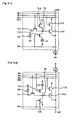
- a solid-state imaging device of the present embodiment is structured in the form of a CMOS image sensor and Fig. 1 is an equivalent circuit diagram for one pixel.
- Each pixel includes a photodiode PD for receiving light and generating photoelectric charges, a transfer transistor Tr1 for transferring the photoelectric charges of the photodiode PD, a floating region FD from which the photoelectric charges are transferred via the transfer transistor Tr1, a storage capacitor element C s for accumulating the photoelectric charges overflowing from the photodiode during accumulating operation, a storage transistor Tr2 for coupling or splitting potentials of the floating region FD and the storage capacitor element C s , a reset transistor Tr3 connected to the floating region FD for discharging the photoelectric charges of the floating region FD, an amplifier transistor Tr4 for amplifying the photoelectric charges of the floating region FD and converting to a voltage signal, and a selection transistor Tr5 coupled to the amplifier transistor for selecting a pixel.
- the CMOS image sensor of the present embodiment includes an integrated array of a plurality of pixels formed in the structure described above.
- the transfer transistor Tr1, the storage transistor Tr2 and the reset transistor Tr3 have gate electrodes connected to drivelines ⁇ T , ⁇ S , ⁇ R , respectively.
- the selection transistor Tr5 has a gate electrode connected to a pixel selection line SL( ⁇ x) adapted to be driven by a line shift register.
- the selection transistor Tr5 has a source and drain on an output to which an output line "out" is connected and is controlled by a row shift register to provide an output. Since the selection transistor Tr5 and the driveline ⁇ x may be suffice to fix a voltage of the floating region FD to an appropriate value so as to enable the operations to select or not to select a pixel, these components may be possibly omitted.
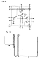
- Fig. 2-1 is a typical cross-sectional view showing a structure corresponding to a part (the photodiode PD, the transfer transistor Tr1, the floating region FD, the storage transistor Tr2 and the storage capacitor element C s ) of each pixel of the CMOS image sensor of the present embodiment.
- an n-type silicon semiconductor substrate (n-sub) 10 is formed with a p-type well (p-well) 11 on which element separating insulation films (20, 21, 22) are formed by a LOCOS process or the like for separating each pixel and the storage capacity element C s .
- a p'-type separating region 12 is formed in the p-type well 11 corresponding to an area below the element separating insulation film 20 for separating the pixels from each other.
- the p-type well 11 is formed with an n-type semiconductor region 13 whose surface layer is formed with a p'-type semiconductor region 14 in a p-n junction by which a photodiode PD of a charge-transfer buried type is formed. Applying appropriate bias to the p-n junction creates a depleted layer that receives incident light LT and generates photoelectric charges due to a photoelectric effect.
- the n-type semiconductor region 13 has a terminal end portion formed in a region sticking out of the p'-type semiconductor region 14.
- An n'-type semiconductor region 15 is formed on the surface layer of the p-type well 11 in an area remote from the stick-out region by a given distance and serves as the floating region FD.
- an n'-type semiconductor region 16 is formed on the surface layer of the p-type well 11 in another area remote from the stick-out region by a given distance.
- a gate electrode 30, made of polysilicon is formed over an upper surface of the p-type well 11 in an area associated with the n-type semiconductor region 13 and the n'-type semiconductor region 15 via a gate insulation film 23 formed of oxide silicon.
- the transfer transistor Tr1 has a source and drain and includes the n-type semiconductor region 13, the n'-type semiconductor region 15 and a channel forming region on the surface layer of the p-type well 11. Further, a gate electrode 31, made of polysilicon, is formed over the upper surface of the p-type well 11 in an area associated with the n'-type semiconductor region 15 and the n'-type semiconductor region 16 via a gate insulation film 24 formed of oxide silicon.
- the storage transistor Tr2 has a source and drain and includes the n'-type semiconductor region 15, the n'-type semiconductor region 16 and a channel forming region on the surface layer of the p-type well 11.
- a p'-type semiconductor region 17 is formed on the surface layer of the p-type well 11 in an area separated by the element separating insulation films (21, 22) to serve as a lower electrode and has an upper layer on which an upper electrode 32, formed of polysilicon or the like, is formed via a capacitor insulation film 25, formed of oxide silicone or the like to thereby form the storage capacitor element C s .
- the transfer transistor Tr1, the storage transistor Tr2 and the storage capacitor element C s are covered with an insulation film that is formed of oxide silicon so as to form opening portions exposed to the n'-type semiconductor regions 15 and 16 and the upper electrode 32 and a wiring 33 is formed and connected to the n'-type semiconductor region 15 while a wiring 34 is formed to connect the n'-type semiconductor region 16 and the upper electrode 32.
- the driveline ⁇ T is connected to the gate electrode 30 of the transfer transistor Tr1 and, also, the driveline ⁇ S is connected to the gate electrode 31 of the storage transistor Tr2.
- the other component parts such as the reset transistor Tr3, the amplifier transistor Tr4, the selection transistor Tr5, the various drivelines ⁇ T , ⁇ S, ⁇ R , ⁇ X and the output line "out", are formed on the semiconductor substrate 10 shown in Fig. 2-1 in areas, not shown, so as to obtain the structure in the equivalent circuit diagram shown in Fig. 1 such that, for instance, the wiring 33 is connected to the amplifier transistor Tr4 that is not shown.
- Fig. 2-2 is a typical potential diagram corresponding to the photodiode PD, the transfer transistor Tr1, the floating region FD, the storage transistor Tr2 and the storage capacitor element C S mentioned above.
- the photodiode PD forms a capacitor C PD with a potential that is relatively shallow and the floating region FD and the storage capacitor C S form a capacitor (C FD , C S ) with a potential that is relatively deep.
- the transfer transistor Tr1 and the storage transistor Tr2 may take two levels depending on on/off states of the transistors.
- Fig. 3-1 is a timing chart showing voltages applied to the drivelines ( ⁇ T , ⁇ S , ⁇ R ) in two levels for on/off states with ⁇ T having three levels additionally including a level represented by (+ ⁇ ).
- the voltage applied to the driveline ⁇ T may take the two levels for ON/OFF states and may preferably take the three levels as represented in the present example for enabling the floating region FD and the storage capacitor element C S to efficiently capture and accumulate an electric charge overflowing from the photodiode PD.
- Figs. 3-1 is a timing chart showing voltages applied to the drivelines ( ⁇ T , ⁇ S , ⁇ R ) in two levels for on/off states with ⁇ T having three levels additionally including a level represented by (+ ⁇ ).
- the voltage applied to the driveline ⁇ T may take the two levels for ON/OFF states and may preferably take the three levels as represented in the present example for enabling the floating region FD and the storage capacitor element C S to efficiently capture and accumulate an electric charge overflowing from
- 3-2 and 3-3 are graphs showing variations in voltage potentials (V PD , V FD , V CS ) of the capacitors (C PD , C FD , C S ) formed of the photodiode PD, the floating region FD and the storage capacitor element C S in the timing charts mentioned above, respectively.
- Fig. 3-2 represents waveforms of the voltage potentials appearing at light intensity less than a level causing a photoelectron generated by the photodiode PD to saturate the capacitor C PD and
- Fig. 3-3 shows voltage waveforms plotted in terms of light intensity greater than the level causing the capacitor C PD to be saturated.
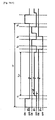
- Figs. 4-1 to 4-4 and Figs. 5-1 to 5-4 correspond to potential diagrams at respective timings of the timing charts.
- noise N 2 A method of reading out noise N 2 for accumulation in a frame memory (storage means), described below, to allow noise N 2 to be utilized in generating an image signal establishes an operation method that provides the highest S/N ratio.
- noise N 1 since noise N 2 is sufficiently less than a value of pre-saturated charges and supersaturated charges during supersaturating operation, noise N 1, described below, may be used in place of noise N 2 .
- noise N 2 of a subsequent frame may be used in place of noise N 2 of the current frame.
- Fig. 4-2 shows a status in which C PD is saturated and pre-saturated charges Q B are accumulated in C PD and supersaturated charges Q A are accumulated in C FD and C S .
- ⁇ T is returned to be off from the level of (+ ⁇ ) and ⁇ S is set to be off to split the potentials of C FD and C S as shown in Fig. 4-3 .
- ⁇ R is set to be on and, as shown in Fig. 4-4 , the photoelectric charges are discharged from C FD for resetting.
- kTC noise newly occurs in C FD as shown in Fig. 5-1 .
- a signal appearing at a reset level in C FD is read out as noise N 1 .
- ⁇ T is set to be on and pre-saturated charges Q B are transferred from C PD to C FD as shown in Fig. 5-2 .
- C PD has a potential shallower than that of C FD and the transfer transistor has a level deeper than that of C PD
- the pre-saturated charges Q B are entirely transferred from C PD to C FD to thereby realize a complete electric charge transfer.
- ⁇ T is returned to be off at time T 3 and a pre-saturated charge signal S 1 is read out from the pre-saturated charges Q B transferred to C FD .
- S 1 + N 1 is actually read out.
- Fig. 5-2 shows a status appearing before ⁇ T is returned to be off.
- ⁇ S is set to be on and, consecutively, ⁇ T is set to be on to couple the potentials of C FD and C S so that the pre-saturated charges Q B in C FD and the supersaturated charges Q A in C S are mixed as shown in Fig. 5-3 .
- ⁇ T is returned to be off at time T 4 and a signal of a sum of the pre-saturated charge signal S 1 and the supersaturated charge signal S 2 is read out from a value of the pre-saturated charges Q B and the supersaturated charges Q A that are spread in C FD + C S .
- FIG. 6 is an equivalent circuit diagram showing an overall circuit structure of the CMOS image sensor of the present embodiment.
- a plurality (with four pieces typically shown in the drawing figure) of pixels is arranged in an array and the respective pixels (Pixel) are connected to the drivelines ( ⁇ T , ⁇ S , ⁇ R , ⁇ X ) controlled by a line shift register SR v , a power supply VDD and ground GND.
- the respective pixels are controlled by the row shift register SR N and the drivelines ( ⁇ S1 +N1 , ⁇ N1 , ⁇ S1' +S2'+N2 , ⁇ N2 ) to provide outputs on the respective output lines at respective timings in four values including the pre-saturated charge signal (S 1 ) + C FD noise (N 1 ), C FD noise (N 1 ), a modulated pre-saturated charge signal (S 1 ') + a modulated supersaturated charge signal (S 2 ') + C FD + Cs noise (N 2 ) and C FD + C S noise (N 2 ).
- CMOS image sensor chip may be formed with a circuit CT b including a difference amplifier DC1.
- Fig. 7 shows a circuit for processing the four signals including the pre-saturated charge signal (Si) + C FD noise (N 1 ), C FD noise (N 1 ), the modulated pre-saturated charge signal (S 1 ') + the modulated supersaturated charge signal (S 2 ') + C FD + Cs noise (N 2 ) and C FD + C S noise (N 2 ) which are output as previously mentioned.
- the pre-saturated charge signal (S 1 ) + C FD noise (N 1 ) and C FD noise (N 1 ) are input to the difference amplifier DC1 to extract a difference between these components for canceling C FD noise (N 1 ) thereby obtaining the pre-saturated charge signal (S 1 ).
- the pre-saturated charge signal (S 1 ) may be digitized using an A/D converter ADC1 depending on needs or an analog signal may be kept intact without providing ADC1.
- the modulated pre-saturated charge signal (S 1 ') + the modulated supersaturated charge signal (S 2 ') + C FD + C S noise (N 2 ) is applied to a difference amplifier DC2 to extract a difference among these components for canceling C FD + C S noise (N 2 ).
- an amplifier AP executes demodulation with a capacitance ratio between C FD and C S for adjustment to the same gain as that of the pre-saturated charge signal (S 1 ) to thereby obtain a sum (S 1 + S 2 ) of the pre-saturated charge signal and the supersaturated charge signal.
- the signal S 1 ' + S 2 ' + N 2 and the signal N 2 may be digitized by A/D converters ADC2, ADC3, provided depending on needs, before these signals are input to the differential amplifier DC2 or an analog signal may be input intact to the difference amplifier DC2 without providing ADC2, ADC3.
- either one of S 1 and S 1 + S 2 is selected and treated as a final output.
- S 1 is input to a comparator CP for comparison with a preset reference voltage V 0 .
- S 1 and S 1 + S 2 are input to a selector SE and either one of S 1 and S 1 + S 2 are selected to be output depending on an output of the comparator CP described above.
- the reference voltage V o is selected to have a voltage potential, appearing prior to the saturation depending on a capacitance of the photodiode PD, which lies at a level of, for instance, approximately 0.3V.
- a circuitry involving such outputs is formed on a CMOS image sensor chip and a circuitry, for the rest of component parts subsequent to the difference amplifier DC1 and the frame memory FM, may be realized as an external part.
- the difference amplifier DC1 may be formed on the CMOS image sensor chip in a manner as mentioned above.
- analog data may be preferably subjected to A/D conversion to perform digitizing operations of analog data, appearing subsequent to the difference amplifier DC1 and the frame memory FM, before they are input to the difference amplifier DC1 and the frame memory FM.
- analog data may be preferable to be preliminarily amplified by an amplifier, not shown, in compliance with an input range of an A/D converter to be used.
- the CMOS image sensor of the present embodiment has a consequence of obtaining two signals including the pre-saturated charge signal (S 1 ) and the sum (S 1 + S 2 ) of the pre-saturated charge signal and the supersaturated charge signal for each pixel and for each field.
- S 1 the pre-saturated charge signal
- S 1 + S 2 the sum of the pre-saturated charge signal and the supersaturated charge signal for each pixel and for each field.
- making judgment whether the photodiode (C PD ) is saturated or nearly close to such a status results in the selection of either S 1 or S 1 + S 2 .
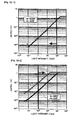
- Fig. 8-1 is a view plotting an electric charge count, resulting from capacitance CFD in a manner described above, in terms of relative light intensity and corresponds to the signal S 1 .
- Fig. 8-2 is a view plotting an electric charge count, resulting from capacitance C FD + C s , in terms of relative light intensity and corresponds to the signal S 1 + S 2 .
- V 0 the reference voltage
- the signal S 1 shown in Fig. 8-1
- the signal S 1 + S 2 shown in Fig. 8-2
- the signal S 1 is less than the signal S 1 + S 2 and the signal S 1 is adopted in low illuminance with no issue arising for a noise level to increase.
- a saturated voltage potential of C FD fluctuates for each pixel with the fluctuations ranging in the order of approximately 1 ⁇ 10 4 to 2 ⁇ 10 4 in terms of an electric charge count.
- the signal is switched to the signal S 1 + S 2 employing capacitance C FD + C s resulting in advantageous effect with no adverse affect from the fluctuations in the saturated voltage potential of C FD .
- an electric charge count of C FD and an electric charge count of C FD + C S match each other throughout vicinities of the reference voltage potential with no issue arising in using either the signal S 1 or the signal S 1 + S 2 in a vicinity of the reference voltage potential.
- Fig. 8-3 is a view showing an overlapped status with the graph (designated as C FD ) shown in Fig. 8-1 , wherein the voltage of the floating region resulting from the use of capacitance C FD is plotted in terms of relative light intensity, and the graph (designated as C FD + C S ) shown in Fig. 8-2 wherein the voltage of the floating region resulting from the use of capacitance C FD + C S is plotted in terms of relative light intensity.
- This view corresponds to a consequence resulting from converting the electric charge count, shown in the graphs of Figs. 8-1 and 8-2 , to a voltage.
- the pre-saturated charge signal (S 1 ) is adopted in the absence of the saturation of the photodiode PD (C PD ) and the sum (S 1 + S 2 ) of the pre-saturated charge signal and the supersaturated charge signal in the presence of the saturation.
- the pre-saturated charge signal (S 1 ) resulting from canceling noise enables high sensitivity and a high S/N ratio to be maintained during low illuminance with no saturation of the photodiode PD.
- the photoelectric charges overflowing from the photodiode are accumulated and taken in the storage capacitor element and using a signal (the sum (S 1 + S 2 ) of the pre-saturated charge signal and the supersaturated charge signal, resulting from canceling noise in the same manner as that previously described, enables the high S/N ratio to be maintained and a wide dynamic range to be realized to an effect on high illuminance.
- the CMOS image sensor of the present embodiment increases sensitivity for high illuminance to achieve a wide dynamic range without causing a drop in sensitivity for low illuminance, as described above, and no power supply voltage is increased from a range in normal use with the resultant capability of matching the miniaturization of a future image sensor. Addition of an element is suppressed into a minimal with no occurrence of enlargement of the pixel in size. Further, since no accumulation time is split for high and low illuminance as experienced in the image sensor of the related art for realizing a wide dynamic range, that is, the accumulation is performed during the same accumulation time without striding over frames, the image sensor of the present embodiment can comply with the shooting of moving images.
- the present embodiment is a modified form of the circuit structure of pixels of the CMOS image sensor of the first embodiment.
- Fig. 9-1 is an equivalent circuit diagram of an example of one pixel in the CMOS image sensor of the present embodiment.
- This embodiment is substantially identical to the equivalent circuit diagram of Fig. 1 and differs from the same in connection between the amplifier transistor Tr4 and the selection transistor Tr5 in a form in which the selection transistor Tr5 is placed in an upper stage area of the amplifier transistor Tr4 and the output of the amplifier transistor Tr4 is connected to the output line "out".
- Such a connection makes it possible to raise a gain of an amplifier of the amplifier transistor Tr4.
- Fig. 9-2 is an equivalent circuit diagram of one pixel in the other example of the CMOS image sensor of the present embodiment.
- This embodiment is substantially identical to the equivalent circuit diagram of Fig. 1 but takes the form of a structure in which the n-channel MOS transistors, forming the five transistors including the transfer transistor Tr1, the storage transistor Tr2, the reset transistor Tr3, the amplifier transistor Tr4 and the selection transistor Tr5, are replaced by p-channel MOS transistors.
- Such replacement enables the realization of an image sensor of a complete charge-transfer type for holes and is suitable when, for instance, using a p-type as a silicon substrate.
- the CMOS image sensor of the present embodiment is able to maintain high sensitivity and a high S/N ratio using the pre-saturated charge signal resulting from canceling noise during the shooting of images in low illuminance with no saturation in the photodiode.
- the photoelectric charges overflowing from the photodiode are accumulated and taken in the storage capacitor element to allow a signal (equivalent to the sum of the pre-saturated charge signal and the supersaturated charge signal) resulting from canceling noise in the same manner as that described above to maintain a high S/N ratio for realizing a wide dynamic range in high illuminance.
- a solid-state imaging device of the present embodiment takes the form of a CCD image sensor.
- Fig. 10-1 is an equivalent circuit diagram of an example of one pixel in the CCD image sensor of the present embodiment.
- first and second charge-couple transfer paths CCD1 and CCD2 are placed in vertically extending directions and driven in two phases with ⁇ V1 and ⁇ V2 .
- a photodiode PD is directly connected to the first charge-couple transfer path CCD1 and connected to the second charge-couple transfer path CCD2 via a transfer transistor Tr1.
- the second charge-couple transfer path CCD2 functions as a storage capacitor element C that accumulates photoelectric charges, overflowing from the photodiode, when the photodiode PD is saturated.
- the first charge-couple transfer path CCD1 transfers pre-saturated charges in low illuminance for readout upon driving CCD.
- the storage capacitor element C S accumulates supersaturated charges in high illuminance and driving the second charge-couple transfer path CCD2, formed of the storage capacitor element C S , results in a consequence of executing the readout intact. Reading out the pre-saturated charges in low illuminance and the supersaturated charges in high illuminance, resulting from the storage capacitor element accumulating the photoelectric charges overflowing from the photodiode, realizes a wide dynamic range in high illuminance.
- Fig. 10-2 is an equivalent circuit diagram of the other example of one pixel in the CCD image sensor of the present embodiment.
- This example corresponds to the form of a structure wherein with the CCD image sensor of the first embodiment, the first charge-couple transfer path CCD1 transfers the pre-saturated charges in low illuminance for readout upon driving CCD.
- the supersaturated charges in high illuminance is read out in the same step as that of reading out the signal in the CMOS image sensor of the first embodiment.
- the storage transistor Tr2 is not required to be connected between the floating region FD and the storage capacitor element C S .
- the present embodiment is a modified form of the circuit structure of the pixel in the CMOS image sensor of the first embodiment.
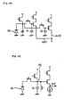
- Fig. 11-1 is an equivalent circuit diagram of the example of one pixel of the CMOS image sensor of the first embodiment.
- Fig. 11-1 is substantially similar to the equivalent circuit diagram of Fig. 1 and directed to a form in which transistors Tr6 to Tr8 are added to form a logarithmic converter circuit that logarithmically converts and reads out the photoelectric charges accumulated in the storage capacitor element C S .
- Providing an output upon executing logarithmic conversion enables the image sensor to comply with the shooting of images in high illuminance to achieve a wide dynamic range.
- permitting the pre-saturated charges and the supersaturated charges to mix with each other provides capability of improving an S/N ratio.
- Fig. 11-2 is an equivalent circuit diagram for the other example of one pixel in the CMOS image sensor of the present embodiment.
- This circuit takes the form of a structure that additionally includes transistors Tr6, Tr7, Tr9 and Tr10 forming a logarithmic converter circuit that logarithmically converts photoelectric charges overflowing from the photodiode for accumulation in the storage capacitor element C S .
- Providing an output upon executing logarithmic conversion in such a way enables the image sensor to comply with the shooting of images in high illuminance to achieve a wide dynamic range.
- logarithmically converting the photoelectric charges for accumulation in the storage capacitor element C S enables the contribution to enhancement of a wide dynamic range even in the presence of a small storage capacitor element C S .
- a solid-state imaging device of the present embodiment takes the form of the same CMOS image sensor as that of the first embodiment and Fig. 12 is an equivalent circuit diagram of one pixel.
- Each pixel comprises the photodiode for receiving light and generating the photoelectric charges, the transfer transistor Tr1 for transferring the photoelectric charges resulting from the photodiode, the floating region FD to which the photoelectric charges are transferred via the transfer transistor Tr1, the storage capacitor element C S for accumulating the photoelectric charges overflowing from the photodiode during accumulating operation, the storage transistor Tr2 for coupling or splitting the potentials of the floating region FD and the storage capacitor element C S , the reset transistor Tr3 formed on the floating region FD and connected thereto through the storage transistor Tr2 for discharging the photoelectric charges of the storage capacitor element C S and the floating region FD, the amplifier transistor Tr4 for amplifying the photoelectric charges in the floating region FD and converting to a voltage signal, and the selection transistor Tr5 coupled to the amplifier transistor for selecting a pixel,
- the CMOS image sensor of the present embodiment includes the integrated array of a plurality of pixels with the structure mentioned above.
- the transfer transistor Tr1, the storage transistor Tr2 and the reset transistor Tr3 have gate electrodes to which the drivelines ⁇ T , ⁇ S , ⁇ R are connected and the selection transistor Tr5 has a gate electrode to which a pixel selection line SL ( ⁇ X ) driven by the line shift register is connected.
- the selection transistor Tr5 has an output including a source and drain to which an output line "out" is connected for providing an output under control of the row shift register.
- the selection transistor Tr5 and the driveline ⁇ X may be configured to fix a voltage of the floating region FD to a suitable value so as to enable the execution of selecting or non-selecting the pixel and, thus, may be omitted.
- Fig. 13 is a typical potential diagram corresponding to the photodiode PD, the transfer transistor Tr1, the floating region FD, the storage transistor Tr2 and the storage capacitor element C S .
- the photodiode PD forms a relatively shallow potential C PD and the floating region FD and the storage capacitor element C S forms relatively deep capacitors (C FD , C S ).
- the transfer transistor Tr1 and the storage transistor Tr2 may take two levels depending on on/off states of the transistors.
- Fig. 14-1 is a timing chart showing voltages applied to the drivelines ( ⁇ T , ⁇ S , ⁇ R ) in on/off states with two levels while ⁇ T has a further additional level represented by (+ ⁇ ).
- the voltage applied to the driveline ⁇ T may take two levels in ON/OFF and may preferably take the form of three levels, like the present example, which enable the floating region FD and the storage capacitor element C S to efficiently capture and accumulate an electric charge overflowing from the photodiode PD.
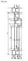
- Fig. 15-1 to Fig. 15-3 and Fig. 16-1 to Fig. 16-3 correspond to potential diagrams at respective timings of the timing charts.
- ⁇ T is set to be off and ⁇ S is set to be on and, under such a status, ⁇ R is set to be on thereby completely discharging photoelectric charges generated in a preceding field for resetting, upon which ⁇ R is set to be off at time T 1 .
- ⁇ S is set to be on with C FD and C S remaining under a coupled condition and, immediately after resetting operation, so-called kTC noise, caused by the resetting operation, occurs in C FD and C S .
- kTC noise caused by the resetting operation
- Fig. 15-2 shows a status where C PD is saturated with pre-saturated charges Q B being accumulated in C PD and supersaturated charges Q A being accumulated in C FD and C S .
- ⁇ T is returned to be off from the level (+ ⁇ ) at the end of the accumulation interval T LT .
- ⁇ S is set to be off to split the potential of C PD and C S as shown in Fig. 15-3 .
- the supersaturated charges Q A are split into Q A1 and Q A2 depending on a capacitance ratio between C FD and C S .
- a signal level of C FD accumulating a partial component Q A1 of the supersaturated charges, is read out as noise N 1 .
- ⁇ T is set to be on and, as shown in Fig. 15-2 , the pre-saturated charges Q B is transferred from C PD to C FD to be mixed with the partial component Q A1 of the supersaturated charges originally accumulated in C FD .
- the potential of C PD is set to be shallower than that of C FD and the level of the transfer transistor is set to be deeper than that of C PD , a complete electric charge transfer can be realized for entirely transferring the pre-saturated charges Q B from C PD to C FD .
- ⁇ T is returned to be off at time T 3 for reading out the pre-saturated charge signal S 1 from the pre-saturated charges Q B transferred to C FD .
- Fig. 16-1 shows a status where ⁇ T is returned to be off.
- ⁇ S is set to be on and ⁇ T is consecutively set to be on causing the potentials of C FD and C S to be coupled to each other.
- the sum of the partial component Q A1 of the supersaturated charges and the partial component Q A2 of the supersaturated charges corresponds to the supersaturated charges Q A prior to the splitting.
- ⁇ T is returned to be off at time T 4 for reading out a signal representing the sum of the pre-saturated charge signal S 1 and the supersaturated charge signal S 2 from the value resulting from the pre-saturated charges Q B and the saturated charges Q A .
- noise N 2 is read out and accumulated in the frame memory once to allow noise N 2 to be utilized during an operation to generate an image signal
- noise N 2 is smaller enough than that of the pre-saturated charges + the supersaturated charges during a supersaturated period and, therefore, noise N 2 of the current frame may be replaced in use by noise N 2 appearing in a subsequent frame.
- the field can be driven in accordance with the timing chart shown in Fig. 14-2 .
- this timing chart differs from the timing chart of Fig. 14-1 in respect of a time period provided for permitting ⁇ T to be set on during the resetting operation of each field. In this case, even the electric charge in C PD can be reliably reset.
- an overall circuit structure or the like takes the same structure as that of the first embodiment.
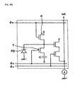
- Fig. 17 shows one example of a layout diagram of approximately one pixel in a case where the CMOS solid-state imaging device of the present embodiment adopts a planar type storage capacitor element.
- the photodiode PD, the storage capacitor element C S and the five transistors Tr1 to Tr5 are placed in a layout, shown in the drawing figure, and in addition thereto, the floating region FD between the transistors Tr1 and Tr2 and the gate electrode of the transistor Tr4 are connected to each other through a lead wire W1. Further, a diffusion layer between the transistors Tr2 and Tr3 and the upper electrode of the storage capacitor element C S are connected to each other via a wiring W2.
- a circuitry can be realized corresponding to the equivalent circuit diagram of the present embodiment shown Fig. 13 .
- the transfer transistor Tr1 has a channel whose width is formed in a size to be wide in an area closer to the photodiode PD and narrow in an area closer to the floating region FD. Therefore, the electric charge, overflowing from the photodiode, can be caused to overflow to the floating region in an efficient manner. In the meantime, permitting the transfer transistor Tr1 to have the channel narrowed in the area closer to the floating region FD enables reduction in capacitance of the floating region FD with the resultant increase in a fluctuation width of a potential with respect to an electric charge accumulated in the floating region FD.
- the pre-saturated charge signal (S 1 ) is adopted in the absence of the saturation of the photodiode PD and the sum (S 1 + S 2 ) of the pre-saturated charge signal and the supersaturated charge signal is adopted in the presence of the saturation.
- the photoelectric charges, overflowing from the photodiode are accumulated and taken in the storage capacitor element and using a signal (the sum (S 1 + S 2 ) of the pre-saturated charge signal and the supersaturated charge signal), obtained by canceling noise in the same manner as mentioned above, enables a high S/N ratio to be maintained and a wide dynamic range to be realized in high illuminance.
- the CMOS image sensor of the present embodiment can increase sensitivity in high illuminance without causing a drop in sensitivity in low illuminance as described above for thereby achieving a wide dynamic range and, in addition, no power supply voltage is caused to exceed beyond a range normally in use with the resultant capability of complying with a need for a future image sensor to be miniaturized. Addition of elements is suppressed to a minimal with no occurrence of an increase in a size of a pixel. Further, since no accumulation time is divided for high illuminance and low illuminance as required in the related art image sensor for realizing a wide dynamic range, that is, since the photoelectric charges are accumulated in the same accumulation interval without striding the frames, the image sensor can comply with the shooting of moving images.
- CMOS image sensor of the present embodiment for a leakage current (FD-leakage) of the floating region FD, a minimal signal of C FD + C S takes supersaturated charges + saturated charges from the photodiode PD. This results in a consequence of handling the greater amount of electric charges than that of the FD-leakage with an advantageous effect with less adverse affect from the FD-leakage.
- the CMOS image sensor of the present embodiment is hard to be adversely affected from variations in saturation of PD.
- the CMOS image sensor of the present embodiment takes the form of a CMOS sensor, based on the CMOS image sensors of the first to fifth embodiments, which takes the form of a structure described below for enabling the suppression of a leakage from the floating region.
- Fig. 18-1 is a cross sectional view showing a detail of a floating region area of the CMOS sensor of the present embodiment.
- the p-type well (p-well) 11 has an active region that is split off by means of an element separating insulation film 20 made of oxide silicon using a LOCOS process.
- a p'-type split region 12 is formed in the p-type well 11 at an area below the separating insulation film 20.
- the p-type well 11 is further formed with a p'-type separating region 12a in an area beneath an end portion 20a of the LOCOS element separating insulation film 20 that is called as a bird's beak.
- the p-type well 11 is formed with a gate electrode 30, made of poly silicon, intervening a gate insulation film 23 formed on a surface of the p-type well 11 and made of oxide silicon in an area remote from the end portion 20a of the element separating insulation film 20 by a given distance.
- the gate electrode has a side portion formed with a sidewall spacer 30a made of, for instance, silicon nitride.
- a surface layer of the p-type well 11 in a position between the gate electrode 30 and the element separating insulation film 20 is formed with an n'-type semiconductor region 15 serving as a floating region FD.
- the n'-type semiconductor region 15 includes a low-concentrated impurity region 15a and a high-concentrated impurity region 15b.
- the CMOS sensor takes the form of a structure in which the low-concentrated impurity region 15a sticks out of an end of the high-concentrated impurity region 15b, that is, in a so-called LDD (Lightly Doped Drain) structure.
- LDD Lightly Doped Drain
- the low-concentrated impurity region 15a is formed in a wide area closer to a vicinity of the end portion 20a of the element separating insulation film 20 and a vicinity of the gate electrode 30 at positions closer to the vicinity of the end portion 20a of the element separating insulation film 20 and the vicinity of the gate electrode 30.
- a transfer transistor Tr1 is structured to have a channel forming region extending from a source and drain, composed of the gate electrode 30 and the n'-type semiconductor region 15, to the surface layer of the p-type well 11.
- the gate electrode 30, the n'-type semiconductor region 15 and the element separating insulation film 20 are covered with an interlayer insulation film, made of oxide silicon, to which a contact reaching the n'-type semiconductor region 15 is open.
- a TiSi layer (or a Ti layer) 41 and a TiN layer 42 are stacked on an upper layer of the n'-type semiconductor region 15 forming a bottom portion of the contact and a contact is buried on an upper layer of the TiN layer to form a tungsten plug 43.
- An upper layer wiring 44 is formed on an upper layer of the interlayer insulation film in connection with the tungsten plug 43.
- the upper layer wiring 44 is formed in a surface area so as to cover the n'-type semiconductor region 15 and is also is connected to the contact to take the same potential as that of the n'-type semiconductor region 15.
- the p'-type separation region 12a is formed beneath the bird's beak of the LOCOS element separating insulation film 20 and the n'-type semiconductor region 15 takes the LDD structure.
- a leakage in the n'-type semiconductor region 15 (floating region FD) can be suppressed.
- the upper layer wiring 44 having the same potential is formed on the n'-type semiconductor region 15 (floating region FD) so as to cover the same in a shielding effect. This enables a surface of the n'-type semiconductor region 15 (floating region FD) to be suppressed from being formed with depletions that are causes of the leakages.
- the CMOS sensor takes the form of a structure that can remarkably suppress a leakage on the n'-type semiconductor region (floating region FD).
- Figs. 18-2 and 18-3 are cross-sectional views showing manufacturing steps of the CMOS sensor shown in Fig. 18-1 .
- the p'-type separating region 12, forming a channel top, and the element separating insulation film 20, employing the LOCOS process are formed in an element separating region of the p-type well 11 and the p'-type separation region 12a is also formed in an area beneath the bird's beak of the element separating insulation film 20.
- the gate insulation film 23 is formed on the surface of the p-type well 11, using, for instance, a thermal oxidation method, and the gate electrode 30 is patterned.
- n-type electrically conductive impurity DPI is ion-implanted so as to define a terminal portion using the gate electrode and the bird's beak of the element separating insulation film 20.
- the low-concentrated impurity region 15a is formed.
- a silicon nitride film is formed on an entire surface by, for instance, a CVD (Chemical Vapor Deposition) and, then, an etchback process is performed to thereby form the sidewall spacer 30a at a side area of the gate electrode 30.
- a resist film PR is formed in a pattern to cover the element separating insulation film 20 so as to allow the resist film PR to stick out from the bird's beak to some extent.
- n-type conductive impurity DP2 so as to define a terminal portion thereof with the sidewall spacer 30a and the resistor film PR, mentioned above, allows the high-concentrated impurity region 15b to be formed.
- a film of oxide silicon is formed on the entire surface by a CVD method for forming an interlayer insulation film to allow the resulting interlayer insulation film to have a contact open to the n'-type semiconductor region 15 and a TiSi layer (or a Ti-layer) 41 is formed by, for instance, a sputtering method.
- a TiN layer 42 is formed and, further, the tungsten plug 43 is buried and formed.
- using, for instance metallic material allows the upper layer wire lead 44 to be formed in a width to cover the n'-type semiconductor region 15, providing the structure shown in Fig. 18-1 .
- CMOS sensor of the present embodiment like the embodiments mentioned above, a wide dynamic range can be realized in high illuminance and, in addition thereto, leakage current in the floating region can be suppressed.
- a CMOS sensor of the present embodiment takes the form of a CMOS sensor, based on the CMOS sensors of the first to sixth embodiments, in which a voltage applied to the driveline ⁇ T takes only two levels in on/off states with no provision of the level (+ ⁇ ) as shown in Fig. 3-1 and enables an electric charge, overflowing from the photodiode during operation of accumulating the electric charges to smoothly shift to a floating region.
- CMOS sensors shown in Figs. 19-1 and 19-2 , include transfer transistors each of a buried channel type having such a semiconductor layer of the same conductor type as that of the channel of the transfer transistor that is formed in the surface of the substrate in which the transfer transistor is formed or in an area of the substrate from a vicinity of the surface down to a predetermined depth.
- Fig. 19-1 is a cross-sectional view of one example of the CMOS sensor of the present embodiment showing areas corresponding to the photodiode PD, the transfer transistor Tr1, the floating region FD and the storage transistor Tr2.
- the n'-type semiconductor region 16, forming a source and drain of the storage transistor Tr2, is connected to the storage capacitor element C S that is not shown.
- an n-type semiconductor region 50 is formed on the substrate in an area below the gate electrode 30 of the transfer transistor Tr1 in a given depth from the surface of the substrate in a way to partially overlap the n-type semiconductor region 13 and the n'-type semiconductor region 15.
- the n-type semiconductor region 50 serves as an n-type region with effective concentration impurity lower than those of the n-type semiconductor region 13 and the n'-type semiconductor region 15.
- the transfer transistor Tr1 is formed in a buried channel and this corresponds to a consequence of a drop occurring in a potential barrier between the photodiode and the floating region. Accordingly, an equivalent potential can be obtained even if no voltage potential, represented by the level (+ ⁇ ) as shown in Fig. 3-1 , is applied to the driveline ⁇ T and an electric charge, overflowing from the photodiode during accumulating operation of the electric charges, can be caused to smoothly shift to the floating region.
- Fig. 19-2 is a cross-sectional view of one example of the CMOS sensor of the present embodiment wherein, like the CMOS sensor shown Fig. 19-1 , the n-type semiconductor region 50 is formed on the substrate in the area below the gate electrode 30 of the transfer transistor Tr1 in the given depth from the surface of the substrate so as to partially overlap the n-type semiconductor region 13 and the n'-type semiconductor region 15. Further, the p'-type semiconductor region 14, formed on the surface layer of the photodiode PD, is formed so as to extend to an area below the gate electrode 30 of the transfer transistor Tr1.
- the transfer transistor Tr1 is formed in the buried channel configuration and this corresponds to a consequence of a drop occurring in a potential barrier between the photodiode and the floating region. Accordingly, an equivalent potential can be obtained even if no voltage potential, represented by the level (+ ⁇ ) as shown in Fig. 3-1 , is applied to the driveline ⁇ T and an electric charge, overflowing from the photodiode during accumulating operation of the electric charges, can be caused to smoothly shift to the floating region.
- CMOS sensors shown in Figs. 20-1 and 20-2 , include transfer transistors each takes the form of a structure including a semiconductor layer that is formed in an area in a predetermined depth of the substrate in which the transfer transistor is formed and is of the same conductive type as that of the channel of the transfer transistor.
- the semiconductor layer reduces a barrier for punch-through of the transfer transistor.
- Fig. 20-1 is a cross-sectional view of one example of the CMOS sensor of the present embodiment showing areas corresponding to the photodiode PD, the transfer transistor Tr1, the floating region FD and the storage transistor Tr2.
- the n'-type semiconductor region 16, forming a source and drain of the storage transistor Tr2, is connected to the storage capacitor element C S that is not shown.
- an n-type semiconductor region 51 is formed in a substrate in an area below the gate electrode 30 of the transfer transistor Tr1 at a region in a given depth from the surface of the substrate and is connected to the n-type semiconductor region 13.
- the above structure corresponds to a consequence of a drop occurring in the barrier for punch-through of the transfer transistor Tr1.
- a punch-through route oriented in a slanted direction from the n-type semiconductor region 51 to the floating region FD serves as an overflow path PA. Accordingly, even if no voltage potential, represented by the level (+ ⁇ ) as shown in Fig. 3-1 , is applied to the driveline ⁇ T , an electric charge, overflowing from the photodiode during accumulating operation of the electric charges, can be caused to punch-through for smooth shift to the floating region.
- Fig. 20-2 is a cross-sectional view of one example of the CMOS sensor of the present embodiment wherein, like the CMOS sensor shown in Fig. 20-1 , an n-type semiconductor region 52 is formed in a substrate in an area below the gate electrode 30 of the transfer transistor Tr1 at a region in a given depth from the surface of the substrate and is connected to the n-type semiconductor region 13. With the present embodiment, the n-type semiconductor region 52 is formed in a further extension extending to a region below the floating region FD.
- the above structure corresponds to a consequence of a drop occurring in a barrier for punch-through of the transfer transistor Tr1.
- a punch-through route extends in a substantially vertical direction from the n-type semiconductor region 52 to the floating region FD and serves as an overflow path PA extending from the photodiode to the floating region FD. Accordingly, even if no voltage potential, represented by the level (+ ⁇ ) as shown in Fig. 3-1 , is applied to the driveline ⁇ T , an electric charge, overflowing from the photodiode during accumulating operation of the electric charges, can be caused to punch-through for smooth shift to the floating region.
- the present embodiment represents a modified form of the embodiment of the storage capacitor element for storing the photoelectric charges overflowing from the photodiode in the various embodiments described above.
- an electrostatic capacitance per 1 ⁇ m 2 lies in a value of approximately 0.3 to 3fF/ ⁇ m 2 even in the light of conditions and a surface efficiency is not very satisfactory accompanied by a difficulty in widening a dynamic range.
- oxide silicon with dielectric constant of 3.9
- material High-k containing some materials such as silicon nitride (ditto with a value of 7.9), Ta 2 O 5 (ditto with 20 to 30), HfO 2 (ditto with a value of 30), ZrO 2 (ditto with a value of 30) and Ra 2 O 3 (ditto with a value of 40 to 50)
- a further increased electrostatic capacitance can be realized and even the planar type, formed in a relatively simplified structure, can realize an image sensor with a wide dynamic range in a value of 100 to 120 dB.
- Fig. 21-1 is a cross-sectional view of a planar type MOS storage capacitor element with the same structure as that of the first embodiment.
- the storage capacitor element C S takes the form of a structure that includes, for instance, a p'-type semiconductor region 17 formed on a surface layer portion of a semiconductor substrate 10 and serving as as a lower electrode, an oxide silicon capacitor insulation film 25 formed on the p'-type semiconductor region 17, and an upper electrode 32, made of polysilicon, formed on the oxide silicon capacitor insulation film 25.
- Fig. 21-2 is a cross-sectional view of a planar type MOS and a junction type storage capacitor element.
- a surface layer of a p-type well 11, formed on an n-type semiconductor substrate 10 has an n'-type semiconductor region 16b, serving as a lower electrode, which is integrally formed with an n'-type semiconductor region 16a serving as a source and drain of a storage transistor.
- An upper electrode 32 is formed over the semiconductor regions 16a, 16b via a capacitor insulation film 25, made of oxide silicon, and thus, a storage capacitor element C S is formed. In this case, the upper electrode 32 is applied with a power supply voltage or ground GND.
- a storage capacitor element, shown in Fig. 22-1 in cross-section, is of a same planar type MOS storage capacitor element similar to that of Fig. 21-1 .
- a capacitor insulation film 25a is made of material High-k such as silicon nitride or Ta 2 O 5 or the like and formed in a larger capacity than that of the storage capacitor element shown in Fig. 21-1 .
- a storage capacitor element, shown in Fig. 22-2 in cross-section, is of a planar type MOS and junction type storage capacitor element similar to that of Fig. 21-2 .
- the capacitor insulation film 25a is made of material High-k such as silicon nitride or Ta 2 O 5 and formed in a larger capacity than that of the storage capacitor element shown in Fig. 21-2 .
- Fig. 23-1 is a cross-sectional view of a stack type storage capacitor element.
- the stack type storage capacitor element takes the form of a structure that includes a lower electrode 37, formed on an element separation insulating film formed on an n-type semiconductor substrate 10, a capacitor insulation film 25 formed on the lower electrode 37, and an upper electrode 38 formed on the capacitor insulation film 25.
- an n'-type semiconductor film 16, serving as a source and drain of a storage transistor, and the lower electrode 37 are connected to each other by a wiring 36.
- the upper electrode 38 is applied with a power supply voltage VDD or ground GND.
- Fig. 23-2 is a cross-sectional view of a cylindrical-shaped stack type storage capacitor element.
- the stack type storage capacitor element takes the form of a structure that includes a cylindrical-shaped lower electrode 37a, coupled to an n'-type semiconductor region 16 serving as a source and drain of a storage transistor, a capacitor insulation film 25, formed on an inner wall surface of the cylindrical-shaped lower electrode 37a, and an upper electrode 38a formed in a way to bury a cylindrically inner portion of the lower electrode 37a via the capacitor insulation film 25.
- the upper electrode 38a is applied with a power supply voltage VDD or ground GND.
- Fig. 24 is a cross-sectional view of a composite storage capacitor element combined with the planar MOS type and the stack type. This example enables the formation of a large capacitor that has a high efficiency in usage of area.
- Fig. 25-1 is a cross-sectional view of a trench type storage capacitor element.
- a trench TC is formed in a way to penetrate through a p-type well 11 of an n-type semiconductor substrate 10 and ends at the n-type substrate.
- An n'-type semiconductor region 18 is formed in an inner wall of the trench TC and plays a role as a lower electrode.
- a capacitor insulation film 25 is formed in a way to cover the inner wall of the trench TC. Using the capacitor insulation film 25 allows the trench TC to be buried to form an upper electrode 40.
- an n'-type semiconductor region 16, playing a role as a source and drain of a storage transistor, and the upper electrode 40 are connected to each other by a wire lead 34.
- Fig. 25-2 is a cross-sectional view of a trench type storage capacitor element having a junction.
- a trench TC is formed in a p-type well 11 of an n-type semiconductor substrate 10.
- An n'-type semiconductor region 16d is formed in an inner wall of the trench TC to play a role as a lower electrode and integral with an n'-type semiconductor region 16c that plays a role as a source and drain of a storage transistor.
- a capacitor insulation film 25 is formed in a way to cover the inner wall of the trench TC and the trench TC is buried by means of the capacitor insulation film 25 to form an upper electrode 40.
- Fig. 26-1 is a cross-sectional view of a trench type storage capacitor element.
- a trench TC is formed in a manner to penetrate through a p-type well 11 of an n-type semiconductor substrate 10 and ends at the n-type substrate.
- An n'-type semiconductor region 18 is formed in an inner wall of a region formed in an area deeper than a certain depth of the trench TC and plays a role as a lower electrode.
- a capacitor insulation film 25 is formed in a way to cover the inner wall of the trench TC.
- the trench TC is buried using the capacitor insulation film 25 to form an upper electrode 40.
- an n'-type semiconductor region 16 is connected to the upper electrode 40 by a wiring 34 and serves as a source and drain of a storage transistor.
- Fig. 26-2 is a cross-sectional view of a trench type storage capacitor element.
- a trench TC is formed in a way to penetrate through a p-type well 11 of an n-type semiconductor substrate 10 and ends at the n-type substrate.
- a p'-type semiconductor region 19 is formed on the inner wall of the trench TC and serves as a lower electrode.
- a capacitor insulation film 25 is formed to cover the inner wall of the trench TC.
- the trench TC is buried using the capacitor insulation film 25 to form an upper electrode 40.
- an n'-type semiconductor region 16 and the upper electrode 40 are connected to each other by a wiring 34 and serves as a source and drain of a storage transistor.
- Fig. 27 is a cross-sectional view of a CMOS sensor having a buried storage capacitor element employing a junction capacitor.
- a p-type epitaxial layer 61 is formed on a p-type silicon semiconductor substrate (p-sub) 60 and an n'-type semiconductor region 62 is formed in areas of the p-type silicon semiconductor substrate 60 and the n'-type semiconductor region 62. That is, a semiconductor region of an n-type (first conductive type) and a semiconductor region of a p-type (second conductive type) are joined to each other and buried in an inner area of a semiconductor substrate of a solid-state imaging device to form a buried storage capacitor element using a junction capacitor.
- the p-type silicon semiconductor substrate 60 and the p-type epitaxial layer region 61 further have areas formed with p'-type separating region 63.
- a p-type semiconductor layer 64 is formed on the p-type epitaxial layer 61 and has a photodiode PD, a transfer transistor Tr1, a floating region FD and a storage transistor Tr2 that are formed in the same steps as those of the various embodiments set forth above.
- the n'-type semiconductor region 62 serves as a source and drain of the storage transistor Tr2 and is formed in a wide area across various areas in which the photodiodes PD, the transfer transistor Tr1, the floating region FD and the storage transistor Tr2 are formed.
- the n'-type semiconductor region 16 serves as a source and drain of the storage transistor Tr2 and is connected to the n'-type semiconductor region 62, forming a storage capacitor element, via an n'-type semiconductor region 65 vertically extending through the p-type semiconductor layer 64.
- Fig. 28 is a cross-sectional view of a CMOS sensor having a buried storage capacitor element using an insulation film capacitor and a junction capacitor.
- the CMOS sensor shown in Fig. 28 , is similar to that of Fig. 27 , and the p-type silicon semiconductor substrate (p-sub) 60 is formed with a first p-type epitaxial layer 61 a and a second p-type epitaxial layer 61 b via an insulation film 60, taking the form of an SOI (Semiconductor on Insulator) substrate in which a semiconductor layer is formed on the semiconductor substrate via an insulation film.
- SOI semiconductor on Insulator
- an n+-type semiconductor region 62 is formed in an area extending across the first p-type epitaxial layer 61 a and the second p-type epitaxial layer 61 b to the insulation film 60a and using an insulation film capacitor between the semiconductor substrate, opposing to the semiconductor region 62, and the semiconductor layer forms a storage capacitor element.
- a junction capacitor is formed between the first p-type epitaxial layer 61 a and the second p-type epitaxial layer 61 b like the storage capacitor element shown in Fig. 27 .
- the other structure is similar to the CMOS sensor shown in Fig. 27 .
- Fig. 29 is a cross-sectional view of a CMOS sensor having a buried storage capacitor element using an insulation film capacitor and a junction capacitor.
- CMOS sensor shown in Fig. 29 , is similar to that of Fig. 28 , a low-concentrated semiconductor region (i-layer) is additionally formed between an n-type semiconductor region 13, forming a photodiode, and an n'-type semiconductor region 62 forming a storage capacitor element.
- the above structure corresponds to a consequence of a drop in a potential barrier between the n-type semiconductor region 13 and the n'-type semiconductor region 62 making an overflow path PA extending from the photodiode to the floating region FD.
- the various storage capacitor elements described above can be applied to any of the embodiments set forth above.
- the storage capacitor elements with such a configuration, mentioned above, are caused to accumulate the photoelectric charges overflowing from the photodiode, enabling the realization of a wide dynamic range in high illuminance.
- a noise level was set to 2e - .
- an electron count involving that of C S lies at a value of 2 ⁇ 10 5 e - during saturation and can realize a dynamic range in a value of 100dB.
- FIG. 30 is a schematic plan view of respective pixels (Pixel) formed upon employing the trench type storage capacitor elements.
- Each pixel (Pixel) includes a photodiode PD, a pixel circuit PC and a trench type storage capacitor element Cap.
- a length of a trench type storage capacitor element in terms of a plane on a planar view lies in a value of approximately 4 ⁇ m ⁇ 2 even in a long one.
- Fig. 31 is a typical view illustrating a size of a trench type storage capacitor element in assumption.
- a trench TC is formed in a p-type well 11 of an n-type semiconductor substrate 10 and has an inner wall formed with a p-type semiconductor region 19 that plays a role as a lower electrode.
- a capacitor insulation film 25, made of oxide silicon, is formed in a way to cover the inner wall of the trench TC. Burying the trench TC using the capacitor insulation film 25 forms an upper electrode 40 in structure.
- a length L is set to 4 ⁇ m ⁇ 2 as described above.
- the trench TC has a depth D of 2 ⁇ m and the capacitor insulation film 25 of oxide silicon (dielectric constant of 3.9) has a film thickness of t ox , with only a side surface of the trench TC taken into consideration, a capacitance lies at a value of 160fF and an electron count during saturation lies at a value of 5 ⁇ 10 5 e - enabling a dynamic range to be realized in a value of 100 to 120dB.
- CMOS image sensor of the present invention a simulation was carried out to obtain a dynamic range that can be achieved when applied with the planar type storage capacitor element mentioned above.
- Fig. 32 is a layout chart of a pixel when applied with the planar type storage capacitor element.
- a photodiode PD, a floating region FD, a storage capacitor element C S and other pixel circuitry were placed to obtain a layout shown in Fig. 32 .
- a result 38fF.
- CMOS image sensor of the present invention assumption was made that a photodiode PD of a pixel having one side with 3 ⁇ m in length had a surface area with an aperture-ratio of 25% and a micro lens was additionally incorporated into the photodiode PD to obtain a substantially aperture-ratio of 80%.
- a photodiode PD of a pixel having one side with 3 ⁇ m in length had a surface area with an aperture-ratio of 25% and a micro lens was additionally incorporated into the photodiode PD to obtain a substantially aperture-ratio of 80%.
- two kinds of 64fF and 640fF were set and a simulation was conducted to obtain a linearity of an output (V) and light intensity (lux) in respect of one phase before the photodiode PD was saturated and another phase in which the photodiode PD was saturated.
- V output
- lux light intensity
- FIG. 33-1 is a view in which the output (V) appearing prior to the saturation of the photodiode PD is plotted in terms of light intensity (lux). Confirmation was made that due to the phase prior to the saturation, both of outputs of the storage capacitor elements with capacitances 64fF and 640fF matched each other and the output (V) and light intensity (lux) had a correlation with high linearity. Further, Fig. 33-2 is a view in which the output (V) appearing subsequent to the saturation of the photodiode PD is plotted in terms of light intensity (lux).
- the present invention is not limited to the above description.
- the embodiments have been described with reference to the solid-state imaging devices, the present invention is not limited to such devices and can achieve a wide dynamic range, high sensitivity and a high S/N ratio, which would be hard to be obtained in the related art practice, in a line sensor including linearly arranged pixels of each solid-state imaging device and an optical sensor using a pixel of each solid-state imaging device intact.
- no particular limitation is intended to shapes of the storage capacitor elements and various methods, heretofore developed to increase a capacitance with the use of a memory storage capacitor element of DRAM, can be adopted.
- the solid-state imaging devices may suffice to take the form of structures in each of which a photodiode and a storage capacitor element, adapted to accumulate photoelectric charges overflowing from the photodiode, are connected to each other via a transfer transistor and may also have application to, in addition to a CMOS image sensor, a CCD.
- a solid-state imaging device of the present invention can be applied to image sensors, needed to have a wide dynamic range, such as a CMOS image sensor or a CCD image sensor to be loaded on a digital camera and a cell-phone or the like.
- a line sensor of the present invention can be applied to a line sensor that needs a wide dynamic range.
- An optical sensor of the present invention can be applied to an optical sensor that needs a wide dynamic range.
- a method of operating a slid-state imaging device according to the present invention can be applied a method of operating an image sensor that needs a wide dynamic range.
Landscapes
- Engineering & Computer Science (AREA)
- Physics & Mathematics (AREA)
- Power Engineering (AREA)
- General Physics & Mathematics (AREA)
- Electromagnetism (AREA)
- Condensed Matter Physics & Semiconductors (AREA)
- Computer Hardware Design (AREA)
- Microelectronics & Electronic Packaging (AREA)
- Signal Processing (AREA)
- Multimedia (AREA)
- Solid State Image Pick-Up Elements (AREA)
- Transforming Light Signals Into Electric Signals (AREA)
- Facsimile Heads (AREA)
Claims (4)
- Procédé d'utilisation d'un dispositif d'imagerie à semi-conducteurs comprenant un réseau intégré d'une pluralité de pixels, chaque pixel possédant une photodiode (PD) pour recevoir la lumière et générer des charges photoélectriques, un transistor de transfert (Tr1) pour transférer les charges photoélectriques, un transistor de stockage (Tr2), une région flottante (FD) couplée à la photodiode (PD) via le transistor de transfert (Tr1), un élément condensateur de stockage (CS) accumulant les charges photoélectriques débordant de la photodiode (PD) via le transistor de transfert (Tr1) et le transistor de stockage (Tr2) au cours d'une opération d'accumulation, et un transistor de réinitialisation (Tr3) connecté à la région flottante, le transistor de stockage (Tr2) couplant ou partageant de manière contrôlable les potentiels de la région flottante et de l'élément condensateur de stockage (CS), le procédé d'utilisation comprenant les étapes consistant à :décharger les charges photoélectriques de la région flottante en réinitialisant le transistor de réinitialisation (Tr3) ;éteindre le transistor de transfert (Tr1) et allumer le transistor de stockage (Tr2) pour décharger les charges photoélectriques de la région flottante (FD) et de l'élément condensateur de stockage (CS), avant d'accumuler les charges ;lire un signal de tension à un niveau de réinitialisation de la région flottante (FD) et de l'élément de condensateur de stockage (CS) ; le procédé d'utilisation étant caractérisé par les étapes consistant à :accumuler dans la photodiode les charges pré-saturées ((QB) parmi les charges photoélectriques générées dans la photodiode et accumuler dans la région flottante (FD) et l'élément condensateur de stockage (CS) des charges sursaturées (QA) débordant de la photodiode dans le même intervalle d'accumulation dans lequel une barrière entre un condensateur de la photodiode et un condensateur de la région flottante (FD) est définie comme étant légèrement plus basse ;éteindre le transistor de stockage (Tr2) pour partager les potentiels de la région flottante (FD) et de l'élément de condensateur de stockage (CS) et lire un signal de tension à un niveau de pré-transfert des charges pré-saturées dans la région flottante (FD) ;allumer le transistor de transfert (Tr1) pour transférer les charges pré-saturées (QB) vers la région flottante (FD) et lire un signal de tension à un niveau de post-transfert des charges pré-saturées (QB) et,allumer le transistor de stockage (Tr2) et, consécutivement, allumer le transistor de transfert pour coupler les potentiels de la région flottante (FD) et de l'élément de condensateur de stockage (CS) pour mélanger les charges pré-saturées (QB) et les charges sursaturées (QA) et lire un signal de tension d'une somme des charges pré-saturées (QB) et des charges sursaturées (QA).
- Procédé d'utilisation du dispositif d'imagerie selon la revendication 1, consistant en outre à :supprimer le bruit d'un signal de tension des charges pré-saturées (QB) en prenant une différence entre un signal de tension des charges pré-saturées (QB) et un signal de tension à un niveau de réinitialisation de la région flottante (FD) :supprimer le bruit d'un signal de tension d'une somme des charges pré-saturées (QB) et des charges sursaturées (QA) en prenant une différence entre le signal de tension de la somme des charges pré-saturées(QB) et des charges sursaturées (QA) et d'un signal de tension à un niveau de réinitialisation de la région flottante (FD) et de l'élément de condensateur de stockage (CS) ;ajuster un gain du signal de tension de la somme des charges pré-saturées et des charges sursaturées afin de rendre le gain sensiblement identique au gain du signal de tension des charges pré-saturées(QB) ; etsélectionner l'un ou l'autre du signal de tension à bruit supprimé des charges pré-saturées (QB) et du signal de tension à bruit supprimé de la somme des charges pré-saturées (QB) et des charges sursaturées (QA) en le comparant à une tension de référence.
- Procédé d'utilisation du dispositif d'imagerie selon la revendication 1, dans lequel :l'étape d'accumulation dans la photodiode des charges pré-saturées (QB) parmi les charges photoélectriques générées dans la photodiode et d'accumulation dans la région flottante (FD) et l'élément de condensateur de stockage (CS) des charges sursaturées (QA) débordant de la photodiode comprend les étapes consistant à :ajuster le potentiel du transistor de transfert (Tr1) à un niveau pour éteindre complètement le transistor de transfert (Tr1) ou à un niveau inférieur à ce niveau.
- Procédé d'utilisation d'un dispositif d'imagerie à semi-conducteurs selon l'une quelconque des revendications 1 à 3,
comprenant en outre l'étape de lecture d'un signal de tension à un niveau de réinitialisation de la région flottante (FD).
Priority Applications (1)
| Application Number | Priority Date | Filing Date | Title |
|---|---|---|---|
| EP12183519.3A EP2533289B1 (fr) | 2004-02-27 | 2005-02-25 | Dispositif d'imagerie, capteur de ligne, capteur optique, et procede d'utilisation de dispositif d'imagerie |
Applications Claiming Priority (3)
| Application Number | Priority Date | Filing Date | Title |
|---|---|---|---|
| JP2004053889 | 2004-02-27 | ||
| JP2004322767 | 2004-11-05 | ||
| PCT/JP2005/003193 WO2005083790A1 (fr) | 2004-02-27 | 2005-02-25 | Dispositif d’imagerie à semi-conducteur, capteur de ligne, capteur optique, et procede d’utilisation de dispositif d’imagerie à semi-conducteur |
Related Child Applications (2)
| Application Number | Title | Priority Date | Filing Date |
|---|---|---|---|
| EP12183519.3A Division-Into EP2533289B1 (fr) | 2004-02-27 | 2005-02-25 | Dispositif d'imagerie, capteur de ligne, capteur optique, et procede d'utilisation de dispositif d'imagerie |
| EP12183519.3A Division EP2533289B1 (fr) | 2004-02-27 | 2005-02-25 | Dispositif d'imagerie, capteur de ligne, capteur optique, et procede d'utilisation de dispositif d'imagerie |
Publications (3)
| Publication Number | Publication Date |
|---|---|
| EP1732134A1 EP1732134A1 (fr) | 2006-12-13 |
| EP1732134A4 EP1732134A4 (fr) | 2010-09-22 |
| EP1732134B1 true EP1732134B1 (fr) | 2012-10-24 |
Family
ID=34914454
Family Applications (2)
| Application Number | Title | Priority Date | Filing Date |
|---|---|---|---|
| EP05710743A Active EP1732134B1 (fr) | 2004-02-27 | 2005-02-25 | Dispositif d'imagerie semi-conducteur, capteur de ligne, capteur optique, et procede d'utilisation de dispositif d'imagerie semi-conducteur |
| EP12183519.3A Active EP2533289B1 (fr) | 2004-02-27 | 2005-02-25 | Dispositif d'imagerie, capteur de ligne, capteur optique, et procede d'utilisation de dispositif d'imagerie |
Family Applications After (1)
| Application Number | Title | Priority Date | Filing Date |
|---|---|---|---|
| EP12183519.3A Active EP2533289B1 (fr) | 2004-02-27 | 2005-02-25 | Dispositif d'imagerie, capteur de ligne, capteur optique, et procede d'utilisation de dispositif d'imagerie |
Country Status (5)
| Country | Link |
|---|---|
| US (3) | US7518143B2 (fr) |
| EP (2) | EP1732134B1 (fr) |
| JP (1) | JP4502278B2 (fr) |
| KR (1) | KR101105617B1 (fr) |
| WO (1) | WO2005083790A1 (fr) |
Families Citing this family (134)
| Publication number | Priority date | Publication date | Assignee | Title |
|---|---|---|---|---|
| US7053967B2 (en) | 2002-05-23 | 2006-05-30 | Planar Systems, Inc. | Light sensitive display |
| WO2003073159A1 (fr) | 2002-02-20 | 2003-09-04 | Planar Systems, Inc. | Ecran photosensible |
| US7009663B2 (en) | 2003-12-17 | 2006-03-07 | Planar Systems, Inc. | Integrated optical light sensitive active matrix liquid crystal display |
| US20080084374A1 (en) | 2003-02-20 | 2008-04-10 | Planar Systems, Inc. | Light sensitive display |
| KR101105617B1 (ko) * | 2004-02-27 | 2012-01-18 | 고쿠리츠다이가쿠호진 도호쿠다이가쿠 | 고체 촬상 장치, 라인 센서, 광 센서 및 고체 촬상 장치의동작 방법 |
| US7773139B2 (en) * | 2004-04-16 | 2010-08-10 | Apple Inc. | Image sensor with photosensitive thin film transistors |
| JP4416668B2 (ja) * | 2005-01-14 | 2010-02-17 | キヤノン株式会社 | 固体撮像装置、その制御方法及びカメラ |
| JP4677258B2 (ja) * | 2005-03-18 | 2011-04-27 | キヤノン株式会社 | 固体撮像装置及びカメラ |
| JP4695902B2 (ja) * | 2005-03-18 | 2011-06-08 | キヤノン株式会社 | 固体撮像装置の製造方法 |
| JP4459099B2 (ja) * | 2005-03-18 | 2010-04-28 | キヤノン株式会社 | 固体撮像装置及びカメラ |
| JP2006294871A (ja) * | 2005-04-11 | 2006-10-26 | Matsushita Electric Ind Co Ltd | 固体撮像装置 |
| KR100790228B1 (ko) * | 2005-12-26 | 2008-01-02 | 매그나칩 반도체 유한회사 | 시모스 이미지 센서 |
| JP5052007B2 (ja) * | 2005-12-28 | 2012-10-17 | 住友電工デバイス・イノベーション株式会社 | 半導体装置 |
| US7492048B2 (en) * | 2006-01-10 | 2009-02-17 | International Business Machines Corporation | CMOS sensors having charge pushing regions |
| JP4747858B2 (ja) * | 2006-01-27 | 2011-08-17 | 船井電機株式会社 | 撮像装置 |
| JP4242880B2 (ja) * | 2006-05-17 | 2009-03-25 | 日本テキサス・インスツルメンツ株式会社 | 固体撮像装置及びその動作方法 |
| JP4835270B2 (ja) * | 2006-06-03 | 2011-12-14 | 株式会社ニコン | 固体撮像素子及びこれを用いた撮像装置 |
| JP4467542B2 (ja) * | 2006-06-15 | 2010-05-26 | 日本テキサス・インスツルメンツ株式会社 | 固体撮像装置 |
| JP4361072B2 (ja) * | 2006-06-15 | 2009-11-11 | 日本テキサス・インスツルメンツ株式会社 | 固体撮像装置及びその製造方法 |
| EP1887626A1 (fr) * | 2006-08-09 | 2008-02-13 | Tohoku University | Capteur optique à grille de débordement et condensateur de stockage |
| US8184191B2 (en) | 2006-08-09 | 2012-05-22 | Tohoku University | Optical sensor and solid-state imaging device |
| US7674648B2 (en) * | 2007-03-21 | 2010-03-09 | Eastman Kodak Company | Extended dynamic range using variable sensitivity pixels |
| KR100904716B1 (ko) * | 2007-06-13 | 2009-06-29 | 삼성전자주식회사 | 수광 효율이 향상된 이미지 센서 |
| JP5205155B2 (ja) * | 2007-08-31 | 2013-06-05 | パナソニック株式会社 | 固体撮像素子 |
| EP2665256B1 (fr) * | 2007-09-05 | 2015-11-18 | Tohoku University | Capteur d'image à semi-conducteur et son procédé de commande |
| US8077237B2 (en) * | 2007-10-16 | 2011-12-13 | Aptina Imaging Corporation | Method and apparatus for controlling dual conversion gain signal in imaging devices |
| US7920193B2 (en) * | 2007-10-23 | 2011-04-05 | Aptina Imaging Corporation | Methods, systems and apparatuses using barrier self-calibration for high dynamic range imagers |
| EP2257947A1 (fr) | 2007-11-28 | 2010-12-08 | Nxp B.V. | Mémoire analogique compacte et précise pour des détecteurs cmos de pixels de formation d'image |
| EP2398055B1 (fr) | 2008-01-10 | 2012-12-12 | Stmicroelectronics Sa | Circuit de pixel pour volet électronique global |
| JP4788742B2 (ja) * | 2008-06-27 | 2011-10-05 | ソニー株式会社 | 固体撮像装置及び電子機器 |
| JP5374941B2 (ja) * | 2008-07-02 | 2013-12-25 | ソニー株式会社 | 固体撮像装置及び電子機器 |
| JP5283216B2 (ja) * | 2008-07-31 | 2013-09-04 | 国立大学法人静岡大学 | 高速電荷転送フォトダイオード、ロックインピクセル及び固体撮像装置 |
| JP5282543B2 (ja) * | 2008-11-28 | 2013-09-04 | ソニー株式会社 | 固体撮像装置、固体撮像装置の駆動方法および撮像装置 |
| JP5251563B2 (ja) * | 2009-02-04 | 2013-07-31 | 日本テキサス・インスツルメンツ株式会社 | 撮像装置 |
| KR101605046B1 (ko) | 2009-07-29 | 2016-03-21 | 삼성전자주식회사 | 싱글 게이트 픽셀 및 싱글 게이트 픽셀 동작 방법 |
| JP5733970B2 (ja) * | 2010-01-15 | 2015-06-10 | キヤノン株式会社 | 焦点検出装置 |
| JP5521682B2 (ja) * | 2010-02-26 | 2014-06-18 | ソニー株式会社 | 固体撮像装置、固体撮像装置の駆動方法、及び、電子機器 |
| US20130113768A1 (en) * | 2010-07-27 | 2013-05-09 | Sharp Kabushiki Kaisha | Display device and drive method for same |
| JP5634194B2 (ja) * | 2010-09-28 | 2014-12-03 | キヤノン株式会社 | 放射線撮像装置及びその制御方法 |
| JP5721405B2 (ja) * | 2010-11-22 | 2015-05-20 | キヤノン株式会社 | 撮像システム、その制御方法及びプログラム |
| JP5664175B2 (ja) | 2010-11-29 | 2015-02-04 | ソニー株式会社 | 固体撮像装置とその駆動方法、及び電子機器 |
| US9310923B2 (en) | 2010-12-03 | 2016-04-12 | Apple Inc. | Input device for touch sensitive devices |
| JP5706212B2 (ja) * | 2011-03-29 | 2015-04-22 | シャープ株式会社 | 固体撮像素子およびその製造方法、電子情報機器 |
| TWI456990B (zh) * | 2011-04-08 | 2014-10-11 | Pixart Imaging Inc | 高動態範圍影像感測電路及高動態範圍影像讀取方法 |
| JP5361938B2 (ja) * | 2011-05-02 | 2013-12-04 | キヤノン株式会社 | 固体撮像装置及びカメラ |
| EP2721431A4 (fr) * | 2011-06-16 | 2015-05-06 | Forstgarten Internat Holding Gmbh | Dispositif numérique de capteur d'images par rayons x |
| US9329703B2 (en) | 2011-06-22 | 2016-05-03 | Apple Inc. | Intelligent stylus |
| US8638320B2 (en) | 2011-06-22 | 2014-01-28 | Apple Inc. | Stylus orientation detection |
| US8928635B2 (en) | 2011-06-22 | 2015-01-06 | Apple Inc. | Active stylus |
| JP6024103B2 (ja) * | 2011-06-30 | 2016-11-09 | ソニー株式会社 | 撮像素子、撮像素子の駆動方法、撮像素子の製造方法、および電子機器 |
| TWI505453B (zh) * | 2011-07-12 | 2015-10-21 | Sony Corp | 固態成像裝置,用於驅動其之方法,用於製造其之方法,及電子裝置 |
| US8253178B1 (en) * | 2011-08-02 | 2012-08-28 | Omnivision Technologies, Inc. | CMOS image sensor with peripheral trench capacitor |
| FR2983972B1 (fr) * | 2011-12-08 | 2013-12-27 | Soc Fr Detecteurs Infrarouges Sofradir | Dispositif de detection de rayonnement electromagnetique impulsionnel |
| TWI533699B (zh) | 2012-01-27 | 2016-05-11 | Sony Corp | A solid-state imaging element and a driving method, and an electronic device |
| JP2013162148A (ja) * | 2012-02-01 | 2013-08-19 | Sony Corp | 個体撮像装置および駆動方法、並びに電子機器 |
| FR2986906B1 (fr) | 2012-02-15 | 2015-06-19 | New Imaging Technologies Sas | Structure de pixel actif a transfert de charge ameliore |
| US9176604B2 (en) | 2012-07-27 | 2015-11-03 | Apple Inc. | Stylus device |
| US9557845B2 (en) | 2012-07-27 | 2017-01-31 | Apple Inc. | Input device for and method of communication with capacitive devices through frequency variation |
| US9652090B2 (en) | 2012-07-27 | 2017-05-16 | Apple Inc. | Device for digital communication through capacitive coupling |
| JP2014199898A (ja) * | 2013-03-11 | 2014-10-23 | ソニー株式会社 | 固体撮像素子および製造方法、並びに、電子機器 |
| US10048775B2 (en) | 2013-03-14 | 2018-08-14 | Apple Inc. | Stylus detection and demodulation |
| US10067580B2 (en) | 2013-07-31 | 2018-09-04 | Apple Inc. | Active stylus for use with touch controller architecture |
| JP6247918B2 (ja) * | 2013-12-09 | 2017-12-13 | 浜松ホトニクス株式会社 | 放射線イメージセンサ |
| JP6366285B2 (ja) * | 2014-01-30 | 2018-08-01 | キヤノン株式会社 | 固体撮像装置 |
| JP6376785B2 (ja) * | 2014-03-14 | 2018-08-22 | キヤノン株式会社 | 撮像装置、および、撮像システム |
| US9686490B2 (en) * | 2014-04-01 | 2017-06-20 | Sensors Unlimited, Inc. | Integrating pixels and methods of operation |
| TWI676280B (zh) * | 2014-04-18 | 2019-11-01 | 日商新力股份有限公司 | 固體攝像裝置及具備其之電子機器 |
| GB2525625B (en) * | 2014-04-29 | 2017-05-31 | Isdi Ltd | Device and method |
| JP6484513B2 (ja) * | 2014-10-08 | 2019-03-13 | 株式会社テクノロジーハブ | 画像センサ |
| US9774802B2 (en) * | 2014-11-10 | 2017-09-26 | Raytheon Company | Method and apparatus for increasing pixel sensitivity and dynamic range |
| CN107112334B (zh) * | 2014-11-17 | 2018-09-04 | 国立大学法人东北大学 | 光传感器及其信号读出方法、以及固体摄像装置及其信号读出方法 |
| JP2016111425A (ja) | 2014-12-03 | 2016-06-20 | ルネサスエレクトロニクス株式会社 | 撮像装置 |
| US10067618B2 (en) | 2014-12-04 | 2018-09-04 | Apple Inc. | Coarse scan and targeted active mode scan for touch |
| WO2016098624A1 (fr) * | 2014-12-18 | 2016-06-23 | ソニー株式会社 | Élément d'analyseur d'images à semi-conducteur, dispositif d'analyseur d'images, et appareil électronique |
| CN105744183B (zh) * | 2014-12-26 | 2020-08-11 | 松下知识产权经营株式会社 | 摄像装置 |
| JP2016139660A (ja) * | 2015-01-26 | 2016-08-04 | 株式会社東芝 | 固体撮像装置 |
| US9490282B2 (en) * | 2015-03-19 | 2016-11-08 | Omnivision Technologies, Inc. | Photosensitive capacitor pixel for image sensor |
| US10236288B2 (en) * | 2015-04-28 | 2019-03-19 | CoolStar Technology, Inc. | Integrated on-chip junction capacitor for power management integrated circuit device |
| US9819882B2 (en) * | 2015-06-05 | 2017-11-14 | Caeleste Cvba | Global shutter high dynamic range sensor |
| JP6551882B2 (ja) | 2015-06-08 | 2019-07-31 | パナソニックIpマネジメント株式会社 | 撮像装置および信号処理回路 |
| DE102015108961A1 (de) * | 2015-06-08 | 2016-12-08 | Pmdtechnologies Gmbh | Bildsensor |
| TWI701819B (zh) * | 2015-06-09 | 2020-08-11 | 日商索尼半導體解決方案公司 | 攝像元件、驅動方法及電子機器 |
| US10341592B2 (en) * | 2015-06-09 | 2019-07-02 | Sony Semiconductor Solutions Corporation | Imaging element, driving method, and electronic device |
| US10805561B2 (en) | 2015-07-27 | 2020-10-13 | Sony Corporation | Solid-state image pickup device and control method therefor, and electronic apparatus |
| TWI704811B (zh) | 2015-07-27 | 2020-09-11 | 日商新力股份有限公司 | 固體攝像裝置及其控制方法、以及電子機器 |
| JP2017055248A (ja) | 2015-09-09 | 2017-03-16 | ルネサスエレクトロニクス株式会社 | 撮像素子 |
| KR102618850B1 (ko) * | 2015-09-10 | 2023-12-27 | 가부시키가이샤 한도오따이 에네루기 켄큐쇼 | 촬상 장치, 모듈, 전자 기기, 및 촬상 장치의 동작 방법 |
| US10879285B2 (en) | 2015-09-11 | 2020-12-29 | Sony Semiconductor Solutions Corporation | Solid-state image pickup device to increase an area efficiency of a silicon interface on the transistor element side and electronic apparatus |
| US9838628B2 (en) * | 2016-03-16 | 2017-12-05 | Sony Corporation | Detecting quantities beyond sensor saturation |
| US10474277B2 (en) | 2016-05-31 | 2019-11-12 | Apple Inc. | Position-based stylus communication |
| KR102268948B1 (ko) * | 2016-10-07 | 2021-06-23 | 고쿠리츠다이가쿠호진 도호쿠다이가쿠 | 광 센서 및 그 신호 판독 방법 그리고 고체 촬상 장치 및 그 신호 판독 방법 |
| US10002986B1 (en) * | 2016-12-19 | 2018-06-19 | Waymo Llc | Hybrid integration of photodetector array with digital front end |
| US10075663B2 (en) * | 2017-01-20 | 2018-09-11 | Semiconductor Components Industries, Llc | Phase detection pixels with high speed readout |
| WO2018155297A1 (fr) * | 2017-02-27 | 2018-08-30 | パナソニックIpマネジメント株式会社 | Dispositif d'imagerie à semi-conducteur |
| US12009379B2 (en) * | 2017-05-01 | 2024-06-11 | Visera Technologies Company Limited | Image sensor |
| JP6796777B2 (ja) * | 2017-05-25 | 2020-12-09 | パナソニックIpマネジメント株式会社 | 固体撮像素子、及び撮像装置 |
| US10917589B2 (en) | 2017-06-26 | 2021-02-09 | Facebook Technologies, Llc | Digital pixel with extended dynamic range |
| US10419701B2 (en) | 2017-06-26 | 2019-09-17 | Facebook Technologies, Llc | Digital pixel image sensor |
| US10686996B2 (en) | 2017-06-26 | 2020-06-16 | Facebook Technologies, Llc | Digital pixel with extended dynamic range |
| US10598546B2 (en) | 2017-08-17 | 2020-03-24 | Facebook Technologies, Llc | Detecting high intensity light in photo sensor |
| US11393867B2 (en) | 2017-12-06 | 2022-07-19 | Facebook Technologies, Llc | Multi-photodiode pixel cell |
| US10559614B2 (en) * | 2018-03-09 | 2020-02-11 | Semiconductor Components Industries, Llc | Dual conversion gain circuitry with buried channels |
| US10969273B2 (en) * | 2018-03-19 | 2021-04-06 | Facebook Technologies, Llc | Analog-to-digital converter having programmable quantization resolution |
| US11004881B2 (en) | 2018-04-03 | 2021-05-11 | Facebook Technologies, Llc | Global shutter image sensor |
| US10812742B2 (en) | 2018-04-18 | 2020-10-20 | Facebook Technologies, Llc | Apparatus and method for determining whether a photodiode saturates and outputting a digital value representing a charge from that photodiode based on that determination |
| US10834344B2 (en) | 2018-06-09 | 2020-11-10 | Facebook Technologies, Llc | Digital pixel with extended dynamic range |
| US11906353B2 (en) | 2018-06-11 | 2024-02-20 | Meta Platforms Technologies, Llc | Digital pixel with extended dynamic range |
| US11089241B2 (en) | 2018-06-11 | 2021-08-10 | Facebook Technologies, Llc | Pixel cell with multiple photodiodes |
| US11089210B2 (en) | 2018-06-11 | 2021-08-10 | Facebook Technologies, Llc | Configurable image sensor |
| US10903260B2 (en) | 2018-06-11 | 2021-01-26 | Facebook Technologies, Llc | Multi-photodiode pixel cell |
| US11463636B2 (en) | 2018-06-27 | 2022-10-04 | Facebook Technologies, Llc | Pixel sensor having multiple photodiodes |
| US10897586B2 (en) * | 2018-06-28 | 2021-01-19 | Facebook Technologies, Llc | Global shutter image sensor |
| JP7150504B2 (ja) | 2018-07-18 | 2022-10-11 | キヤノン株式会社 | 固体撮像装置及びその駆動方法 |
| US10931884B2 (en) | 2018-08-20 | 2021-02-23 | Facebook Technologies, Llc | Pixel sensor having adaptive exposure time |
| US11956413B2 (en) | 2018-08-27 | 2024-04-09 | Meta Platforms Technologies, Llc | Pixel sensor having multiple photodiodes and shared comparator |
| JP7356214B2 (ja) | 2018-09-04 | 2023-10-04 | キヤノン株式会社 | 撮像装置、その製造方法及びカメラ |
| CN109254800B (zh) * | 2018-09-30 | 2021-11-16 | 联想(北京)有限公司 | 一种设备信息处理方法、电子设备及服务器 |
| US11595602B2 (en) | 2018-11-05 | 2023-02-28 | Meta Platforms Technologies, Llc | Image sensor post processing |
| CN109327666B (zh) * | 2018-11-20 | 2020-11-06 | 京东方科技集团股份有限公司 | 像素感应电路及其驱动方法、图像传感器、电子设备 |
| US11102430B2 (en) | 2018-12-10 | 2021-08-24 | Facebook Technologies, Llc | Pixel sensor having multiple photodiodes |
| KR102710266B1 (ko) * | 2019-01-07 | 2024-09-27 | 삼성전자주식회사 | 이미지 센서 및 이의 제조 방법 |
| US11218660B1 (en) | 2019-03-26 | 2022-01-04 | Facebook Technologies, Llc | Pixel sensor having shared readout structure |
| CN113544851A (zh) * | 2019-03-28 | 2021-10-22 | 松下知识产权经营株式会社 | 固态成像设备 |
| US11943561B2 (en) | 2019-06-13 | 2024-03-26 | Meta Platforms Technologies, Llc | Non-linear quantization at pixel sensor |
| WO2020261817A1 (fr) * | 2019-06-25 | 2020-12-30 | ソニーセミコンダクタソリューションズ株式会社 | Élément d'imagerie à semi-conducteurs et procédé de fabrication d'élément d'imagerie à semi-conducteurs |
| US11936998B1 (en) | 2019-10-17 | 2024-03-19 | Meta Platforms Technologies, Llc | Digital pixel sensor having extended dynamic range |
| JPWO2021131397A1 (fr) * | 2019-12-26 | 2021-07-01 | ||
| US11902685B1 (en) | 2020-04-28 | 2024-02-13 | Meta Platforms Technologies, Llc | Pixel sensor having hierarchical memory |
| US11910114B2 (en) | 2020-07-17 | 2024-02-20 | Meta Platforms Technologies, Llc | Multi-mode image sensor |
| US11956560B2 (en) | 2020-10-09 | 2024-04-09 | Meta Platforms Technologies, Llc | Digital pixel sensor having reduced quantization operation |
| US20240038808A1 (en) * | 2020-12-28 | 2024-02-01 | Sony Semiconductor Solutions Corporation | Solid-state imaging device and electronic apparatus |
| US12022218B2 (en) | 2020-12-29 | 2024-06-25 | Meta Platforms Technologies, Llc | Digital image sensor using a single-input comparator based quantizer |
| US11509848B2 (en) * | 2021-01-11 | 2022-11-22 | Microsoft Technology Licensing, Llc | Photodiode assembly |
| WO2024038828A1 (fr) * | 2022-08-17 | 2024-02-22 | ソニーセミコンダクタソリューションズ株式会社 | Dispositif de détection de lumière |
Family Cites Families (47)
| Publication number | Priority date | Publication date | Assignee | Title |
|---|---|---|---|---|
| JPH03270579A (ja) * | 1990-03-20 | 1991-12-02 | Fujitsu Ltd | 赤外線撮像装置 |
| JPH0590556A (ja) | 1990-05-11 | 1993-04-09 | Olympus Optical Co Ltd | 固体撮像素子 |
| US5905279A (en) * | 1996-04-09 | 1999-05-18 | Kabushiki Kaisha Toshiba | Low resistant trench fill for a semiconductor device |
| JP3403061B2 (ja) | 1998-03-31 | 2003-05-06 | 株式会社東芝 | 固体撮像装置 |
| US6690423B1 (en) | 1998-03-19 | 2004-02-10 | Kabushiki Kaisha Toshiba | Solid-state image pickup apparatus |
| US6657663B2 (en) * | 1998-05-06 | 2003-12-02 | Intel Corporation | Pre-subtracting architecture for enabling multiple spectrum image sensing |
| JP3592106B2 (ja) * | 1998-11-27 | 2004-11-24 | キヤノン株式会社 | 固体撮像装置およびカメラ |
| JP2001197370A (ja) * | 2000-01-06 | 2001-07-19 | Minolta Co Ltd | 固体撮像装置 |
| US8379126B2 (en) | 1999-06-24 | 2013-02-19 | Konica Minolta Holdings, Inc. | Image-sensing apparatus |
| US6204524B1 (en) * | 1999-07-14 | 2001-03-20 | Micron Technology, Inc. | CMOS imager with storage capacitor |
| JP3668926B2 (ja) * | 1999-08-27 | 2005-07-06 | 株式会社ルネサステクノロジ | 光インタコネクション受信モジュール |
| US6667502B1 (en) * | 1999-08-31 | 2003-12-23 | Micron Technology, Inc. | Structurally-stabilized capacitors and method of making of same |
| US6486504B1 (en) * | 1999-10-26 | 2002-11-26 | Eastman Kodak Company | CMOS image sensor with extended dynamic range |
| JP2001285720A (ja) * | 2000-04-03 | 2001-10-12 | Fuji Film Microdevices Co Ltd | Mos型固体撮像装置および電子カメラ |
| JP3558589B2 (ja) | 2000-06-14 | 2004-08-25 | Necエレクトロニクス株式会社 | Mos型イメージセンサ及びその駆動方法 |
| JP4374745B2 (ja) * | 2000-07-19 | 2009-12-02 | コニカミノルタホールディングス株式会社 | 固体撮像装置 |
| JP3493405B2 (ja) * | 2000-08-31 | 2004-02-03 | ミノルタ株式会社 | 固体撮像装置 |
| AU2001293062A1 (en) * | 2000-09-25 | 2002-04-08 | Foveon, Inc. | Active pixel sensor with noise cancellation |
| KR100542691B1 (ko) | 2001-07-27 | 2006-01-16 | 매그나칩 반도체 유한회사 | 필팩터를 증가시킬 수 있는 씨모스 이미지 센서 및 그구동 방법 |
| DE10142590A1 (de) * | 2001-08-31 | 2003-04-03 | Infineon Technologies Ag | Verfahren zur Seitenwandverstärkung von Resiststrukturen und zur Herstellung von Strukturen mit reduzierter Strukturgröße |
| JP4006207B2 (ja) * | 2001-09-27 | 2007-11-14 | シャープ株式会社 | 電荷検出装置並びにそれを含むmos型固体撮像装置およびccd型固体撮像装置 |
| US6951822B2 (en) * | 2001-09-28 | 2005-10-04 | Infineon Technologies North America Corp. | Method for forming inside nitride spacer for deep trench device DRAM cell |
| JP3984814B2 (ja) | 2001-10-29 | 2007-10-03 | キヤノン株式会社 | 撮像素子、その撮像素子を用いた放射線撮像装置及びそれを用いた放射線撮像システム |
| JP3723124B2 (ja) | 2001-12-14 | 2005-12-07 | 株式会社東芝 | 固体撮像装置 |
| US7429764B2 (en) * | 2002-02-27 | 2008-09-30 | Canon Kabushiki Kaisha | Signal processing device and image pickup apparatus using the same |
| US6960796B2 (en) * | 2002-11-26 | 2005-11-01 | Micron Technology, Inc. | CMOS imager pixel designs with storage capacitor |
| US7075049B2 (en) * | 2003-06-11 | 2006-07-11 | Micron Technology, Inc. | Dual conversion gain imagers |
| US7230292B2 (en) * | 2003-08-05 | 2007-06-12 | Micron Technology, Inc. | Stud electrode and process for making same |
| US7067385B2 (en) * | 2003-09-04 | 2006-06-27 | Micron Technology, Inc. | Support for vertically oriented capacitors during the formation of a semiconductor device |
| US7125781B2 (en) * | 2003-09-04 | 2006-10-24 | Micron Technology, Inc. | Methods of forming capacitor devices |
| KR101105617B1 (ko) * | 2004-02-27 | 2012-01-18 | 고쿠리츠다이가쿠호진 도호쿠다이가쿠 | 고체 촬상 장치, 라인 센서, 광 센서 및 고체 촬상 장치의동작 방법 |
| US7387939B2 (en) * | 2004-07-19 | 2008-06-17 | Micron Technology, Inc. | Methods of forming semiconductor structures and capacitor devices |
| US7202127B2 (en) * | 2004-08-27 | 2007-04-10 | Micron Technology, Inc. | Methods of forming a plurality of capacitors |
| US7439152B2 (en) * | 2004-08-27 | 2008-10-21 | Micron Technology, Inc. | Methods of forming a plurality of capacitors |
| US7320911B2 (en) * | 2004-12-06 | 2008-01-22 | Micron Technology, Inc. | Methods of forming pluralities of capacitors |
| JP4459099B2 (ja) * | 2005-03-18 | 2010-04-28 | キヤノン株式会社 | 固体撮像装置及びカメラ |
| US7557015B2 (en) * | 2005-03-18 | 2009-07-07 | Micron Technology, Inc. | Methods of forming pluralities of capacitors |
| US7517753B2 (en) * | 2005-05-18 | 2009-04-14 | Micron Technology, Inc. | Methods of forming pluralities of capacitors |
| US7544563B2 (en) * | 2005-05-18 | 2009-06-09 | Micron Technology, Inc. | Methods of forming a plurality of capacitors |
| KR100640657B1 (ko) * | 2005-07-25 | 2006-11-01 | 삼성전자주식회사 | 반도체 소자의 미세 패턴 형성 방법 |
| US7199005B2 (en) * | 2005-08-02 | 2007-04-03 | Micron Technology, Inc. | Methods of forming pluralities of capacitors |
| US7393789B2 (en) * | 2005-09-01 | 2008-07-01 | Micron Technology, Inc. | Protective coating for planarization |
| US7557013B2 (en) * | 2006-04-10 | 2009-07-07 | Micron Technology, Inc. | Methods of forming a plurality of capacitors |
| US7902081B2 (en) * | 2006-10-11 | 2011-03-08 | Micron Technology, Inc. | Methods of etching polysilicon and methods of forming pluralities of capacitors |
| US7785962B2 (en) * | 2007-02-26 | 2010-08-31 | Micron Technology, Inc. | Methods of forming a plurality of capacitors |
| US7682924B2 (en) * | 2007-08-13 | 2010-03-23 | Micron Technology, Inc. | Methods of forming a plurality of capacitors |
| US7759193B2 (en) * | 2008-07-09 | 2010-07-20 | Micron Technology, Inc. | Methods of forming a plurality of capacitors |
-
2005
- 2005-02-25 KR KR1020067019971A patent/KR101105617B1/ko active IP Right Grant
- 2005-02-25 WO PCT/JP2005/003193 patent/WO2005083790A1/fr active Application Filing
- 2005-02-25 EP EP05710743A patent/EP1732134B1/fr active Active
- 2005-02-25 EP EP12183519.3A patent/EP2533289B1/fr active Active
- 2005-02-25 US US10/590,659 patent/US7518143B2/en active Active
- 2005-02-25 JP JP2006510483A patent/JP4502278B2/ja active Active
-
2008
- 2008-12-04 US US12/328,438 patent/US8120016B2/en active Active
-
2009
- 2009-03-04 US US12/397,769 patent/US7820467B2/en active Active
Also Published As
| Publication number | Publication date |
|---|---|
| JP4502278B2 (ja) | 2010-07-14 |
| JPWO2005083790A1 (ja) | 2007-11-29 |
| EP2533289A1 (fr) | 2012-12-12 |
| US7820467B2 (en) | 2010-10-26 |
| US20090140305A1 (en) | 2009-06-04 |
| WO2005083790A1 (fr) | 2005-09-09 |
| KR20070004782A (ko) | 2007-01-09 |
| US20070131991A1 (en) | 2007-06-14 |
| EP1732134A1 (fr) | 2006-12-13 |
| US20090225210A1 (en) | 2009-09-10 |
| US7518143B2 (en) | 2009-04-14 |
| EP2533289B1 (fr) | 2017-08-30 |
| EP1732134A4 (fr) | 2010-09-22 |
| KR101105617B1 (ko) | 2012-01-18 |
| US8120016B2 (en) | 2012-02-21 |
Similar Documents
| Publication | Publication Date | Title |
|---|---|---|
| EP1732134B1 (fr) | Dispositif d'imagerie semi-conducteur, capteur de ligne, capteur optique, et procede d'utilisation de dispositif d'imagerie semi-conducteur | |
| EP2942813B1 (fr) | Capteur optique et dispositif d'imagerie à l'état solide | |
| US8184191B2 (en) | Optical sensor and solid-state imaging device | |
| JP4497366B2 (ja) | 光センサおよび固体撮像装置 | |
| EP1868377B1 (fr) | Capteur de lumiere, dispositif de collecte d image a semi-conducteur et procede pour faire fonctionner le dispositif de collecte d image a semi-conducteur | |
| US7235831B2 (en) | Light-receiving element and photoelectric conversion device | |
| JP4499819B2 (ja) | 固体撮像装置 | |
| JP4467542B2 (ja) | 固体撮像装置 | |
| US7800673B2 (en) | Solid-state imaging device, optical sensor and method of operating solid-state imaging device | |
| JP4361072B2 (ja) | 固体撮像装置及びその製造方法 | |
| JP3667220B2 (ja) | 固体撮像装置、撮像システム及び固体撮像装置の駆動方法 | |
| JP2006217410A5 (fr) | ||
| JP2004312039A (ja) | 光電変換素子 | |
| JPH09199703A (ja) | 光電変換装置と半導体集積回路 | |
| KR101277990B1 (ko) | 광학 센서 및 고체 촬상 장치 | |
| JP2006228962A (ja) | 固体撮像装置および電子情報機器 | |
| JP2005005512A (ja) | 固体撮像装置 | |
| JP2005101627A (ja) | 光電変換装置 |
Legal Events
| Date | Code | Title | Description |
|---|---|---|---|
| PUAI | Public reference made under article 153(3) epc to a published international application that has entered the european phase |
Free format text: ORIGINAL CODE: 0009012 |
|
| 17P | Request for examination filed |
Effective date: 20060926 |
|
| AK | Designated contracting states |
Kind code of ref document: A1 Designated state(s): DE FR GB NL |
|
| DAX | Request for extension of the european patent (deleted) | ||
| RBV | Designated contracting states (corrected) |
Designated state(s): DE FR GB NL |
|
| RAP1 | Party data changed (applicant data changed or rights of an application transferred) |
Owner name: NATIONAL UNIVERSITY CORPORATION TOHOKU UNVERSITY |
|
| A4 | Supplementary search report drawn up and despatched |
Effective date: 20100819 |
|
| 17Q | First examination report despatched |
Effective date: 20101222 |
|
| GRAP | Despatch of communication of intention to grant a patent |
Free format text: ORIGINAL CODE: EPIDOSNIGR1 |
|
| GRAS | Grant fee paid |
Free format text: ORIGINAL CODE: EPIDOSNIGR3 |
|
| GRAA | (expected) grant |
Free format text: ORIGINAL CODE: 0009210 |
|
| AK | Designated contracting states |
Kind code of ref document: B1 Designated state(s): DE FR GB NL |
|
| REG | Reference to a national code |
Ref country code: GB Ref legal event code: FG4D |
|
| REG | Reference to a national code |
Ref country code: DE Ref legal event code: R096 Ref document number: 602005036660 Country of ref document: DE Effective date: 20121220 |
|
| REG | Reference to a national code |
Ref country code: NL Ref legal event code: T3 |
|
| PLBE | No opposition filed within time limit |
Free format text: ORIGINAL CODE: 0009261 |
|
| STAA | Information on the status of an ep patent application or granted ep patent |
Free format text: STATUS: NO OPPOSITION FILED WITHIN TIME LIMIT |
|
| 26N | No opposition filed |
Effective date: 20130725 |
|
| REG | Reference to a national code |
Ref country code: DE Ref legal event code: R097 Ref document number: 602005036660 Country of ref document: DE Effective date: 20130725 |
|
| REG | Reference to a national code |
Ref country code: FR Ref legal event code: PLFP Year of fee payment: 12 |
|
| REG | Reference to a national code |
Ref country code: FR Ref legal event code: PLFP Year of fee payment: 13 |
|
| REG | Reference to a national code |
Ref country code: FR Ref legal event code: PLFP Year of fee payment: 14 |
|
| REG | Reference to a national code |
Ref country code: DE Ref legal event code: R082 Ref document number: 602005036660 Country of ref document: DE Representative=s name: GLAWE DELFS MOLL PARTNERSCHAFT MBB VON PATENT-, DE |
|
| PGFP | Annual fee paid to national office [announced via postgrant information from national office to epo] |
Ref country code: NL Payment date: 20240108 Year of fee payment: 20 |
|
| PGFP | Annual fee paid to national office [announced via postgrant information from national office to epo] |
Ref country code: DE Payment date: 20231229 Year of fee payment: 20 Ref country code: GB Payment date: 20240109 Year of fee payment: 20 |
|
| PGFP | Annual fee paid to national office [announced via postgrant information from national office to epo] |
Ref country code: FR Payment date: 20240103 Year of fee payment: 20 |