EP1658648B1 - Herstellungsverfahren für ein organisches elektronisches bauteil mit hochaufgelöster strukturierung - Google Patents
Herstellungsverfahren für ein organisches elektronisches bauteil mit hochaufgelöster strukturierung Download PDFInfo
- Publication number
- EP1658648B1 EP1658648B1 EP04762661A EP04762661A EP1658648B1 EP 1658648 B1 EP1658648 B1 EP 1658648B1 EP 04762661 A EP04762661 A EP 04762661A EP 04762661 A EP04762661 A EP 04762661A EP 1658648 B1 EP1658648 B1 EP 1658648B1
- Authority
- EP
- European Patent Office
- Prior art keywords
- laser
- electronic component
- conductive
- structuring
- organic
- Prior art date
- Legal status (The legal status is an assumption and is not a legal conclusion. Google has not performed a legal analysis and makes no representation as to the accuracy of the status listed.)
- Expired - Lifetime
Links
- 238000004519 manufacturing process Methods 0.000 title claims abstract description 10
- 238000000034 method Methods 0.000 title claims description 31
- 239000004020 conductor Substances 0.000 claims abstract description 23
- 239000000463 material Substances 0.000 claims description 16
- 239000000758 substrate Substances 0.000 claims description 12
- 238000013532 laser treatment Methods 0.000 claims description 10
- 239000007769 metal material Substances 0.000 claims description 5
- 238000004544 sputter deposition Methods 0.000 claims description 3
- 238000000151 deposition Methods 0.000 claims 2
- 230000008021 deposition Effects 0.000 claims 1
- 239000011368 organic material Substances 0.000 abstract description 8
- 230000005669 field effect Effects 0.000 abstract description 2
- 229910052751 metal Inorganic materials 0.000 description 5
- 239000002184 metal Substances 0.000 description 5
- 229920001002 functional polymer Polymers 0.000 description 3
- 239000007788 liquid Substances 0.000 description 3
- 239000004065 semiconductor Substances 0.000 description 3
- 239000000956 alloy Substances 0.000 description 2
- 229910045601 alloy Inorganic materials 0.000 description 2
- 229920003023 plastic Polymers 0.000 description 2
- 239000004033 plastic Substances 0.000 description 2
- 229920000642 polymer Polymers 0.000 description 2
- 239000007787 solid Substances 0.000 description 2
- 239000000126 substance Substances 0.000 description 2
- 230000007704 transition Effects 0.000 description 2
- OKTJSMMVPCPJKN-UHFFFAOYSA-N Carbon Chemical compound [C] OKTJSMMVPCPJKN-UHFFFAOYSA-N 0.000 description 1
- RYGMFSIKBFXOCR-UHFFFAOYSA-N Copper Chemical compound [Cu] RYGMFSIKBFXOCR-UHFFFAOYSA-N 0.000 description 1
- 229920001609 Poly(3,4-ethylenedioxythiophene) Polymers 0.000 description 1
- BQCADISMDOOEFD-UHFFFAOYSA-N Silver Chemical compound [Ag] BQCADISMDOOEFD-UHFFFAOYSA-N 0.000 description 1
- 230000002745 absorbent Effects 0.000 description 1
- 239000002250 absorbent Substances 0.000 description 1
- 229910052782 aluminium Inorganic materials 0.000 description 1
- XAGFODPZIPBFFR-UHFFFAOYSA-N aluminium Chemical compound [Al] XAGFODPZIPBFFR-UHFFFAOYSA-N 0.000 description 1
- 229910052799 carbon Inorganic materials 0.000 description 1
- 239000006229 carbon black Substances 0.000 description 1
- 150000001875 compounds Chemical class 0.000 description 1
- 230000001143 conditioned effect Effects 0.000 description 1
- 229910052802 copper Inorganic materials 0.000 description 1
- 239000010949 copper Substances 0.000 description 1
- 238000004049 embossing Methods 0.000 description 1
- 238000005530 etching Methods 0.000 description 1
- 230000002349 favourable effect Effects 0.000 description 1
- 229910052732 germanium Inorganic materials 0.000 description 1
- GNPVGFCGXDBREM-UHFFFAOYSA-N germanium atom Chemical compound [Ge] GNPVGFCGXDBREM-UHFFFAOYSA-N 0.000 description 1
- PCHJSUWPFVWCPO-UHFFFAOYSA-N gold Chemical compound [Au] PCHJSUWPFVWCPO-UHFFFAOYSA-N 0.000 description 1
- 229910052737 gold Inorganic materials 0.000 description 1
- 239000010931 gold Substances 0.000 description 1
- 239000000976 ink Substances 0.000 description 1
- 238000010297 mechanical methods and process Methods 0.000 description 1
- 239000000155 melt Substances 0.000 description 1
- 239000002923 metal particle Substances 0.000 description 1
- 150000002739 metals Chemical class 0.000 description 1
- 239000000203 mixture Substances 0.000 description 1
- 230000003287 optical effect Effects 0.000 description 1
- 125000002524 organometallic group Chemical group 0.000 description 1
- 238000000059 patterning Methods 0.000 description 1
- 238000000206 photolithography Methods 0.000 description 1
- 229920000767 polyaniline Polymers 0.000 description 1
- 229920001296 polysiloxane Polymers 0.000 description 1
- 238000003825 pressing Methods 0.000 description 1
- 229910052710 silicon Inorganic materials 0.000 description 1
- 239000010703 silicon Substances 0.000 description 1
- 229910052709 silver Inorganic materials 0.000 description 1
- 239000004332 silver Substances 0.000 description 1
- 150000003384 small molecules Chemical class 0.000 description 1
- 238000011282 treatment Methods 0.000 description 1
- 238000007740 vapor deposition Methods 0.000 description 1
Images


Classifications
-
- H—ELECTRICITY
- H10—SEMICONDUCTOR DEVICES; ELECTRIC SOLID-STATE DEVICES NOT OTHERWISE PROVIDED FOR
- H10K—ORGANIC ELECTRIC SOLID-STATE DEVICES
- H10K71/00—Manufacture or treatment specially adapted for the organic devices covered by this subclass
- H10K71/60—Forming conductive regions or layers, e.g. electrodes
-
- H—ELECTRICITY
- H10—SEMICONDUCTOR DEVICES; ELECTRIC SOLID-STATE DEVICES NOT OTHERWISE PROVIDED FOR
- H10K—ORGANIC ELECTRIC SOLID-STATE DEVICES
- H10K10/00—Organic devices specially adapted for rectifying, amplifying, oscillating or switching; Organic capacitors or resistors having potential barriers
- H10K10/40—Organic transistors
- H10K10/46—Field-effect transistors, e.g. organic thin-film transistors [OTFT]
- H10K10/462—Insulated gate field-effect transistors [IGFETs]
- H10K10/468—Insulated gate field-effect transistors [IGFETs] characterised by the gate dielectrics
- H10K10/471—Insulated gate field-effect transistors [IGFETs] characterised by the gate dielectrics the gate dielectric comprising only organic materials
-
- H—ELECTRICITY
- H10—SEMICONDUCTOR DEVICES; ELECTRIC SOLID-STATE DEVICES NOT OTHERWISE PROVIDED FOR
- H10K—ORGANIC ELECTRIC SOLID-STATE DEVICES
- H10K10/00—Organic devices specially adapted for rectifying, amplifying, oscillating or switching; Organic capacitors or resistors having potential barriers
- H10K10/80—Constructional details
-
- H—ELECTRICITY
- H10—SEMICONDUCTOR DEVICES; ELECTRIC SOLID-STATE DEVICES NOT OTHERWISE PROVIDED FOR
- H10K—ORGANIC ELECTRIC SOLID-STATE DEVICES
- H10K71/00—Manufacture or treatment specially adapted for the organic devices covered by this subclass
- H10K71/10—Deposition of organic active material
- H10K71/12—Deposition of organic active material using liquid deposition, e.g. spin coating
- H10K71/13—Deposition of organic active material using liquid deposition, e.g. spin coating using printing techniques, e.g. ink-jet printing or screen printing
-
- H—ELECTRICITY
- H10—SEMICONDUCTOR DEVICES; ELECTRIC SOLID-STATE DEVICES NOT OTHERWISE PROVIDED FOR
- H10K—ORGANIC ELECTRIC SOLID-STATE DEVICES
- H10K71/00—Manufacture or treatment specially adapted for the organic devices covered by this subclass
- H10K71/10—Deposition of organic active material
- H10K71/18—Deposition of organic active material using non-liquid printing techniques, e.g. thermal transfer printing from a donor sheet
Definitions
- the invention relates to a mass production suitable manufacturing method for an organic electronic component with high-resolution structuring, in particular an organic field effect transistor (OFET) with a small source-drain distance.
- OFET organic field effect transistor
- the switching frequency and / or the switching speed of integrated digital circuits is significantly influenced not least by the channel length "1". There has therefore been no lack of attempts to keep this channel length as small as possible, that is to provide a chip for an organic electronic component with the highest possible structuring.
- the object of the invention is to provide a large-scale and favorable method for producing an electronic component of predominantly organic material, in particular to provide a method for producing a high-resolution structure of a functionn layer with a small source-drain distance.
- Solution to the problem and object of the invention is a method for producing an organic electronic component in which for producing a conductor track and / or an electrode, a lower layer and / or the substrate is treated with a laser, thereby at least one recess and / or a region modified by laser treatment is produced in the lower layer and / or the substrate, characterized in that metallic material is sputtered and / or evaporated in the depression and / or on the area modified by laser treatment and excess metallic material is wiped off in a process step following the application of this material, without sputtering on the areas of the lower layer modified by laser treatment / or vapor deposition applied material thereby removed and / or the wells are emptied.
- the distance "1" between two electrodes or between an electrode and a trace smaller 20 ⁇ m.
- excess conductive material is wiped off in a process step subsequent to the application of the material and / or the filling of the depressions with this material, without conductive material from the roughened area and / or from the recess with the roughened bottom in FIG noticeable extent would be removed.
- the application of the conductive material and / or the filling of the depressions can be carried out by various techniques: it can be vapor-deposited or sputtered on.
- the lower layer and / or the substrate is treated with a pulsed laser, for example with pulse lengths of a few 10 ns. Only a few pulses can be enough.
- modified and / or roughened regions and / or depressions produced by laser structuring are characterized in that the contact surface for the conductive material has been treated with laser.
- modified areas and / or recesses generated by laser differ from the areas and / or depressions that have not been treated or impressed, for example, where the excess conductive material distributed around the recess does not exist in the latter wipe without major losses.
- the excess material is simply removed on the non-laser modified areas of the lower layer and / or the substrate, for example mechanically (by Wiping with towels and / or a rubber roller) and the structuring is complete.
- the excess can also be removed with a mechanical method again.
- the combination of these two conductive layers as an electrode or as a conductor now has a high conductivity and has the right work function.
- the structuring of the lowermost (lower) conductive layer (layers) can take place temporally immediately after its application; it can also take place simultaneously with the structuring of the upper layers.
- the structuring of the lower layers may also be done subsequently, after the patterning of the upper conductive layers (e.g., an upper already patterned layer may serve as an etch resistance).
- conductive material is not intended to be limited in any way herein since quite different types of conductive materials have already been used successfully at the site.
- a conductive material for example, a metal, an alloy, a metal paste or an organic conductive compound can be vapor-deposited, sputtered or scribed or otherwise applied. The only thing that matters is that introduced conductive material adheres to the laser-roughened surface.
- Preferred metals include silver, gold, aluminum, copper, etc. and any desired mixtures, alloys of these components, which can be applied in gaseous, liquid, ink or metal paste (metal particles in a liquid medium) and also as a solid.
- Preferred organic materials which can also be combined with a lower conductive layer, for example of metal are PANI, PEDOT and carbon black.
- Modified is used here for areas of a lower layer or a substrate that are altered by laser treatment.
- the roughness of the modified regions is greater than that of the unmodified.
- step A3 B3 and C3 conductive material is applied over a large area.
- a further conductive layer for example of organic material or functional polymer, is applied to the still unstructured highly conductive, for example metallic, layer (Y). This can now be removed mechanically (B5). If the highly conductive layer can not be mechanically removed (patterned), a different (e.g., chemical) method is used after process step B5 to pattern the highly conductive layer. The highly conductive layer (x) is covered at the "modified” or roughened areas and can not be removed here (B5). After chemical structuring (e.g., an etching process), in (B6), the combination of the highly conductive (e.g., metallic) and the conductive (e.g., polymeric) layers is in a patterned form.
- chemical structuring e.g., an etching process
- the substrate is drawn between rolls in a roll-to-roll process.
- recesses and / or modified or roughened areas in the substrate or a lower layer are then produced with a laser, for example an excimer laser, through a mask.
- a laser for example an excimer laser
- the excimer laser may be equipped with optical lens systems so that the pits / areas may not necessarily be the same size as the mask dictates.
- any conductive material present between the recesses / regions is removed by means of an absorbent roll in a roll-to-roll process, for example.
- the reel spins slower than the other reels, effectively wiping.
- organic material or “functional material” or “(functional) polymer” here includes all types of organic, organometallic and / or organic-inorganic plastics (hybrids), in particular those which are referred to in English as “plastics” , These are all types of materials, with the exception of semiconductors, which form the classical diodes (germanium, silicon).
- a limitation in the dogmatic sense of organic material as a carbon-containing material is therefore not provided, but is also intended to the widespread use of eg silicones.
- polymer in the functional polymer is historically conditioned and thus contains no statement about the presence of an actual polymeric compound.
- an organic electronic component such as an OFET, which can certainly also comprise metallic components and layers, can be produced economically with high switching speed and high reliability. It has been found that recesses and / or areas which are produced with a laser, the application of conductive organic material hold different than the conventional recesses / structurings and that therefore with this method tracks organic and metallic nature are faster and easier to produce as for other methods.
Landscapes
- Engineering & Computer Science (AREA)
- Manufacturing & Machinery (AREA)
- Electrodes Of Semiconductors (AREA)
- Thin Film Transistor (AREA)
- Manufacturing Of Printed Wiring (AREA)
- Liquid Deposition Of Substances Of Which Semiconductor Devices Are Composed (AREA)
- Laser Beam Processing (AREA)
- Graft Or Block Polymers (AREA)
- Adhesives Or Adhesive Processes (AREA)
- Dental Preparations (AREA)
- Internal Circuitry In Semiconductor Integrated Circuit Devices (AREA)
Description
- Die Erfindung betrifft ein massenfertigungstaugliches Herstellungsverfahren für ein organisches elektronisches Bauteil mit hochaufgelöster Strukturierung, insbesondere einen organischen Feld-Effekt-Transistor (OFET) mit kleinem Source-Drain-Abstand.
- Die Schaltfrequenz und/oder die Schaltgeschwindigkeit integrierter digitaler Schaltungen wird nicht zuletzt von der Kanallänge "1" maßgeblich beeinflusst. Es hat deshalb nicht an Versuchen gefehlt, diese Kanallänge möglicht klein zu halten, das heißt einen Chip für ein organisches elektronisches Bauteil zu schaffen mit möglichst hoch aufgelöster Strukturierung.
- Bekannt sind organische elektronische Bauteile, insbesondere OFETs mit hochaufgelöster Strukturierung und kleinem Source-Drain-Abstand "1". Bislang werden diese jedoch in aufwendigen Prozessschritten, die mit hohen Kosten verbunden sind, hergestellt. Diese Prozessschritte sind unwirtschaftlich und umfassen regelmäßig Fotolithographie, wobei Vertiefungen in einer unteren Schicht oder im Substrat fotolithographisch erzeugt werden, damit eine Leiterbahn mit der erforderlichen Kapazität gebildet werden kann. Diese Vertiefungen sind muldenförmig und haben keine scharfen Konturen. Der Boden dieser Vertiefungen bleibt unverändert.
- Aus der
WO 2002/47183 - Aufgabe der Erfindung ist es, ein großtechnisches und günstiges Verfahren zur Herstellung eines elektronischen Bauteils aus vorwiegend organischem Material anzugeben, insbesondere ein Verfahren zur Herstellung einer hochaufgelösten Struktur einer Funktinsschicht mit einem kleinen Source-Drain-Abstand, zu schaffen.
- Lösung der Aufgabe und Gegenstand der Erfindung ist ein Verfahren zur Herstellung eines organischen elektronischen Bauteils bei dem zur Herstellung einer Leiterbahn und/oder einer Elektrode eine untere Schicht und/oder das Substrat mit einem Laser behandelt wird, so dass dadurch zumindest eine Vertiefung und/oder ein durch Laserbehandlung veränderter Bereich in der unteren Schicht und/oder dem Substrat erzeugt wird, dadurch charakterisiert, dass
in die Vertiefung und/oder auf den durch Laserbehandlung veränderten Bereich metallisches Material aufgesputtert und/oder aufgedampft wird und überflüssiges metallisches Material in einem dem Aufbringen dieses Materials folgenden Prozessschritt abgewischt wird, ohne dass das auf die durch Laserbehandlung veränderten Bereiche der unteren Schicht durch Sputtern und/oder Aufdampfen aufgebrachte Material dabei entfernt und/oder die Vertiefungen entleert werden. - Nach einer Ausführungsform der Erfindung ist der Abstand "1" zwischen zwei Elektroden oder zwischen einer Elektrode und einer Leiterbahn kleiner 20µm. Das entspricht einer hohen Auflösung der Strukturierung, die besonders bevorzugt sogar unter 10 µm, insbesondere noch wenigere µm beträgt. Durch die Erfindung werden Leckströme zwischen den Leiterbahnen und/oder Elektroden vermieden und deshalb kann der Abstand "1" dazwischen minimiert werden.
- Nach einer Ausführungsform des Verfahrens wird überschüssiges leitfähiges Material in einem auf die Aufbringung des Materials und/oder die Befüllung der Vertiefungen mit diesem Material folgenden Prozessschritt abgewischt, ohne dass dabei leitfähiges Material aus dem aufgerauten Bereich und/oder aus der Vertiefung mit dem aufgerauten Boden in merklichem Umfang wieder entfernt würde.
- Das Aufbringen des leitfähigen Materials und/oder die Befüllung der Vertiefungen kann nach verschiedenen Techniken erfolgen: Es kann aufgedampft oder aufgesputtert werden.
- Nach einer Ausführungsform des Verfahrens wird die untere Schicht und/oder das Substrat mit einem gepulsten Laser, beispielsweise mit Pulslängen von einigen 10 ns, behandelt. Dabei können bereits wenige Pulse ausreichen.
- Die durch Laserstrukturierung erzeugten modifizierten und/oder aufgerauten Bereiche und/oder Vertiefungen zeichnen sich dadurch aus, dass die Auflagefläche für das leitfähige Material mit Laser behandelt wurde. Dadurch unterscheiden sich modifizierte Bereiche und/oder Vertiefungen, die mit Laser erzeugt werden von den Bereichen und/oder Vertiefungen, die nicht oder beispielsweise durch Einprägen behandelt wurden, wo sich bei letzterem das überflüssige leitfähige Material, das um die Vertiefung herum verteilt ist, nicht ohne große Verluste abwischen lässt.
- Für den Fall, dass die Austrittsarbeit (bezogen auf den Halbleiter) des leitfähigen Materials für das geplante elektronische Bauteil passend ist, wird das überschüssige Material einfach auf den nicht durch Laser veränderten Bereichen der unteren Schicht und/oder des Substrats entfernt, beispielsweise mechanisch (durch Wischen mit Tüchern und/oder einer Gummirolle) und die Strukturierung ist abgeschlossen.
- Falls die Austrittsarbeit nicht auf den Halbleiter abgestimmt ist, kann zusätzlich z.B. eine schlecht leitende Schicht aufgebraucht werden, deren Überschuss ebenfalls mit einer mechanischen Methode wieder entfernt werden kann. Die Kombination dieser beiden leitfähigen Schichten als Elektrode oder als Leiterbahn hat nun eine große Leitfähigkeit und besitzt die passende Austrittsarbeit.
- Die Strukturierung der untersten (unteren) leitfähigen Schicht (Schichten) kann zeitlich sofort nach deren Auftragung erfolgen, sie kann auch gleichzeitig mit der Strukturierung der oberen Schichten geschehen.
- Die Strukturierung der unteren Schichten kann ebenfalls nachträglich, nach der Strukturierung der oberen leitfähigen Schichten erfolgen (z.B. kann eine obere bereits strukturierte Schicht als Ätzwiderstand dienen).
- Der Begriff "leitfähiges Material" soll hier in keiner Weise eingeschränkt werden, da ganz verschiedene Arten von leitfähigen Materialien an der Stelle bereits erfolgreich eingesetzt wurden.
- Als leitfähiges Material kann beispielsweise ein Metall, eine Legierung, eine Metallpaste oder eine organische leitfähige Verbindung aufgedampft, aufgesputtert oder eingerakelt oder sonst wie aufgebracht werden. Entscheidend ist nur, dass das eingebrachte leitfähige Material auf der vom Laser aufgerauten Oberfläche haftet.
- Als bevorzugte Metalle werden Silber, Gold, Aluminium, Kupfer etc. sowie beliebige Mischungen, Legierungen dieser Komponenten genannt, die gasförmig, flüssig, als Tinte oder Metallpaste (Metallpartikel in einem flüssigen Medium) und auch als Feststoff aufgebracht werden können.
- Bevorzugte organische Materialien, die sich eben auch mit einer unteren leitfähigen Schicht, beispielsweise aus Metall kombinieren lassen, sind PANI, PEDOT und Carbon Black.
- "Modifiziert" wird hier gebraucht für Bereiche einer unteren Schicht oder eines Substrats, die durch Laserbehandlung verändert sind.
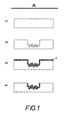
- Im folgenden wird die Erfindung noch anhand dreier Figuren näher erläutert, die beispielhaft und schematisch wiedergeben, wie im Querschnitt gesehen erfindungsgemäß eine Leiterbahn/Elektrode hergestellt wird.
- Bilder A bis C zeigen ein Substrat und/oder eine untere Schicht, die durch ein Verfahren nach der Erfindung behandelt werden:
- A1, B1 und C1 zeigen ein gereinigtes Substrat oder eine gereinigte untere Schicht. Diese wird zunächst durch Laserbehandlung so modifiziert, dass ein Bereich mit einer modifizierten und/oder aufgerauten Oberfläche und/oder eine Vertiefung entsteht (Figuren A2, B2 und C2). Möglich ist auch, dass durch die Behandlung mit Laser eine vorhandene Rauhigkeit der Oberfläche beseitigt wird und der modifizierte Bereich demnach eine geringere Rauhigkeit hat als der nicht durch Laserbehandlung modifizierte.
- Gemäß den Figuren A2, B2 und C2 ist jedoch die Rauhigkeit der modifizierten Bereiche größer als die der nicht modifizierten.
- Im folgenden Prozessschritt A3, B3 und C3 wird großflächig leitfähiges Material aufgebracht.
- Danach wird das überschüssige Material entfernt, es bilden sich bevorzugt scharf abgezeichnete Bereiche in denen leitfähiges Material ein- und/oder aufgebracht ist und andere, die frei von leitfähigem Material sind siehe Figur A4.
- Gemäß der Ausführungsform B wird im Prozessschritt B4 auf die noch unstrukturierte hochleitfähige, beispielsweise metallische Schicht noch eine weitere leitfähige Schicht, beispielsweise aus organischem Material oder Funktionspolymer aufgebracht (Y). Diese kann nun mechanisch entfernt werden (B5). Falls die hochleitfähige Schicht nicht mechanisch entfernt (strukturiert) werden kann, wird nach dem Prozessschritt B5 eine andersartige (z.B. chemische) Methode gewählt, um die hochleitfähige Schicht zu strukturieren. Die hochleitfähige Schicht (x) wird an den "modifizierten" oder aufgerauten Stellen bedeckt und kann hier nicht entfernt werden (B5). Nach der chemischen Strukturierung (z.B. ein Ätzprozess) liegt in (B6) die Kombination der hochleitfähigen (beispielsweise metallischen) und der leitfähigen (beispielsweise polymeren) Schicht in strukturierter Form vor.
- Bei C4 wird ebenfalls eine weitere leitfähige Schicht aufgebracht und anschließend werden beide leitfähigen Schichten mechanische strukturiert (C5).
- Mit dem Prozess nach der Erfindung können leitfähige Strukturen hergestellt werden, die:
- aus mehreren Schichten (versch. Leitfähigkeit) bestehen um z.B. die passende Austrittsarbeit zu gewährleisten.
- hochleitfähig bzw. im "Paket" hochleitfähig sind.
- kostengünstig sind, da nur wenige (3,4,5) Prozessschritte benötigt werden.
- die benötigte Auflösung haben (möglichst kleine Struktur)
- die auf einem massenfertigungstauglichen und schnellen Prozess basieren.
- Die Vorteile liegen auch in der einfachen Herstellungsmethode da nur 3 Prozessschritte benötigt werden (z.B. Laserstrukturierung , leitfähige Schicht aufbringen, Strukturierung der leitfähigen Schicht). Beispielsweise können durch die Verwendung von metallischen Leitern (fest oder flüssig) wiederum beispielsweise in Kombination mit weiteren Leitern aus organischem Material sehr hoch leitfähige kleine Strukturen erstellt werden, ohne das ein Spannungsabfall in den Leiterbahnen problematisch wird. Zusätzlich kann die Austrittsarbeit angepasst werden. Mit Verwendung dieser Technik kann die Schaltungsgröße minimiert werden, wodurch sich ebenfalls die Kosten in gleichem Maße reduzieren.
- Das Substrat wird beispielsweise im Rolle-zu-Rolle-Verfahren zwischen mehreren Walzen hindurchgezogen. Im ersten Arbeitsgang werden dann mit einem Laser, beispielsweise einem Excimer-Laser, durch eine Maske Vertiefungen und/oder modifizierte oder aufgeraute Bereiche im Substrat oder einer unteren Schicht erzeugt. Der Excimer-Laser ist gegebenenfalls mit optischen Linsensystemen ausgestattet, so dass die Vertiefungen/Bereiche nicht unbedingt in derselben Größe abgebildet werden wie die Maske sie vorgibt.
- Bei der mechanischen Strukturierung wird eventuell vorhandenes leitfähiges Material zwischen den Vertiefungen/Bereichen beispielsweise mit einer saugfähigen Rolle im roll-to-roll Verfahren entfernt. Die Rolle dreht sich beispielsweise langsamer als die anderen Rollen, so dass effektiv gewischt wird. Der Begriff "organisches Material" oder "Funktionsmaterial" oder "(Funktions-)Polymer" umfasst hier alle Arten von organischen, metallorganischen und/oder organisch-anorganischen Kunststoffen (Hybride), insbesondere die, die im Englischen z.B. mit "plastics" bezeichnet werden. Es handelt sich um alle Arten von Stoffen mit Ausnahme der Halbleiter, die die klassischen Dioden bilden (Germanium, Silizium). Eine Beschränkung im dogmatischen Sinn auf organisches Material als Kohlenstoff enthaltendes Material ist demnach nicht vorgesehen, vielmehr ist auch an den breiten Einsatz von z.B. Siliconen gedacht. Weiterhin soll der Term keiner Beschränkung im Hinblick auf die Molekülgröße, insbesondere auf polymere und/oder oligomere Materialien unterliegen, sondern es ist durchaus auch der Einsatz von "small molecules" möglich. Der Wortbestandteil "polymer" im Funktionspolymer ist historisch bedingt und enthält insofern keine Aussage über das Vorliegen einer tatsächlich polymeren Verbindung.
- Durch die Erfindung wird erstmals ein Verfahren vorgestellt, mit dem ein organisches elektronisches Bauelement wie ein OFET, der durchaus auch metallische Komponenten und Schichten umfassen kann, mit hoher Schaltgeschwindigkeit und hoher Zuverlässigkeit wirtschaftlich hergestellt werden kann. Es hat sich gezeigt, dass Vertiefungen und/oder Bereiche, die mit einem Laser hergestellt werden, die Aufbringung von leitfähigem organischen Material anders halten als die herkömmlichen Vertiefungen/Strukturierungen und, dass deshalb mit dieser Methode Leiterbahnen organische und metallischer Natur schneller und besser herstellbar sind als nach anderen Methoden.
Claims (4)
- Verfahren zur Herstellung eines organischen elektronischen Bauteils bei dem zur Herstellung einer Leiterbahn und/oder einer Elektrode eine untere Schicht und/oder das Substrat (1) mit einem Laser (3) behandelt wird, so dass dadurch ein durch Laserbehandlung veränderter Bereich (5) in der unteren Schicht und/oder dem Substrat (1) erzeugt wird,
dadurch charakterisiert, dass
auf den durch Laserbehandlung veränderten Bereich (5) metallisches Material durch Sputtern und/oder Aufdampfen aufgebracht wird und überschüssiges metallisches Material in einem dem Aufbringen dieses Materials folgenden Prozessschritt (8) abgewischt wird, ohne dass das auf die durch Laserbehandlung veränderten Bereiche (5) der unteren Schicht (1) aufgebrachte Material dabei entfernt wird. - Verfahren nach Anspruch 1, bei dem die durch Aufsputtern und/oder Aufdampfen von metallischem Material auf die durch Laserbehandlung veränderten Bereiche (5) erhaltene leitfähige Schicht mechanisch strukturiert wird.
- Verfahren nach einem der Ansprüche 1 oder 2, bei dem ein gepulster Laser (3), beispielsweise ein Excimer-Laser (3) eingesetzt wird.
- Verfahren nach einem der Ansprüche 1 bis 3, das in einem kontinuierlichen roll-to-roll Prozess durchgeführt wird.
Applications Claiming Priority (2)
| Application Number | Priority Date | Filing Date | Title |
|---|---|---|---|
| DE10339036A DE10339036A1 (de) | 2003-08-25 | 2003-08-25 | Organisches elektronisches Bauteil mit hochaufgelöster Strukturierung und Herstellungsverfahren dazu |
| PCT/DE2004/001816 WO2005022663A1 (de) | 2003-08-25 | 2004-08-14 | Organisches elektronisches bauteil mit hochaufgelöster strukturierung und herstellungsverfahren dazu |
Publications (2)
| Publication Number | Publication Date |
|---|---|
| EP1658648A1 EP1658648A1 (de) | 2006-05-24 |
| EP1658648B1 true EP1658648B1 (de) | 2009-11-25 |
Family
ID=34223146
Family Applications (1)
| Application Number | Title | Priority Date | Filing Date |
|---|---|---|---|
| EP04762661A Expired - Lifetime EP1658648B1 (de) | 2003-08-25 | 2004-08-14 | Herstellungsverfahren für ein organisches elektronisches bauteil mit hochaufgelöster strukturierung |
Country Status (7)
| Country | Link |
|---|---|
| US (1) | US7479670B2 (de) |
| EP (1) | EP1658648B1 (de) |
| JP (1) | JP2007503712A (de) |
| CN (1) | CN1853289A (de) |
| AT (1) | ATE450057T1 (de) |
| DE (2) | DE10339036A1 (de) |
| WO (1) | WO2005022663A1 (de) |
Cited By (1)
| Publication number | Priority date | Publication date | Assignee | Title |
|---|---|---|---|---|
| DE102010042503A1 (de) | 2010-10-15 | 2012-04-19 | Siemens Aktiengesellschaft | Lasersystem zur Bearbeitung von Oberflächen sowie entsprechendes Verfahren |
Families Citing this family (4)
| Publication number | Priority date | Publication date | Assignee | Title |
|---|---|---|---|---|
| DE10339036A1 (de) | 2003-08-25 | 2005-03-31 | Siemens Ag | Organisches elektronisches Bauteil mit hochaufgelöster Strukturierung und Herstellungsverfahren dazu |
| DE102005031448A1 (de) | 2005-07-04 | 2007-01-11 | Polyic Gmbh & Co. Kg | Aktivierbare optische Schicht |
| DE102017116540B4 (de) * | 2017-07-21 | 2026-04-16 | Pictiva Displays International Limited | Organisches elektronisches Bauelement und Verfahren zur Herstellung eines organischen elektronischen Bauelements |
| AT17082U1 (de) * | 2020-04-27 | 2021-05-15 | Zkw Group Gmbh | Verfahren zur befestigung eines elektronischen bauteils |
Family Cites Families (216)
| Publication number | Priority date | Publication date | Assignee | Title |
|---|---|---|---|---|
| GB723598A (en) | 1951-09-07 | 1955-02-09 | Philips Nv | Improvements in or relating to methods of producing electrically conductive mouldings from plastics |
| US3512052A (en) | 1968-01-11 | 1970-05-12 | Gen Motors Corp | Metal-insulator-semiconductor voltage variable capacitor with controlled resistivity dielectric |
| US3769096A (en) | 1971-03-12 | 1973-10-30 | Bell Telephone Labor Inc | Pyroelectric devices |
| JPS543594B2 (de) | 1973-10-12 | 1979-02-24 | ||
| DE2407110C3 (de) | 1974-02-14 | 1981-04-23 | Siemens AG, 1000 Berlin und 8000 München | Sensor zum Nachweis einer in einem Gas oder einer Flüssigkeit einthaltenen Substanz |
| JPS5638918Y2 (de) | 1977-10-25 | 1981-09-10 | ||
| JPS54101176A (en) | 1978-01-26 | 1979-08-09 | Shinetsu Polymer Co | Contact member for push switch |
| US4442019A (en) | 1978-05-26 | 1984-04-10 | Marks Alvin M | Electroordered dipole suspension |
| US4246298A (en) | 1979-03-14 | 1981-01-20 | American Can Company | Rapid curing of epoxy resin coating compositions by combination of photoinitiation and controlled heat application |
| JPS5641938U (de) | 1979-09-10 | 1981-04-17 | ||
| US4340057A (en) | 1980-12-24 | 1982-07-20 | S. C. Johnson & Son, Inc. | Radiation induced graft polymerization |
| JPS5846719U (ja) | 1981-09-25 | 1983-03-29 | 本州ダンボ−ル工業株式会社 | トレ− |
| JPS59145576A (ja) | 1982-11-09 | 1984-08-21 | ザイトレツクス・コ−ポレ−シヨン | プログラム可能なmosトランジスタ |
| DE3321071A1 (de) | 1983-06-10 | 1984-12-13 | Basf Ag | Druckschalter |
| DE3338597A1 (de) | 1983-10-24 | 1985-05-02 | GAO Gesellschaft für Automation und Organisation mbH, 8000 München | Datentraeger mit integriertem schaltkreis und verfahren zur herstellung desselben |
| JPS60117769U (ja) | 1984-01-14 | 1985-08-09 | 菊地 桂一 | 掛けぶとんのずり落ち防止具 |
| US4554229A (en) | 1984-04-06 | 1985-11-19 | At&T Technologies, Inc. | Multilayer hybrid integrated circuit |
| JPS61167854U (de) | 1985-04-10 | 1986-10-17 | ||
| JPS6265472A (ja) | 1985-09-18 | 1987-03-24 | Toshiba Corp | Mis型半導体素子 |
| DE3768112D1 (de) | 1986-03-03 | 1991-04-04 | Toshiba Kawasaki Kk | Strahlungsdetektor. |
| DE3751376T2 (de) | 1986-10-13 | 1995-11-16 | Canon Kk | Schaltungselement. |
| JP2728412B2 (ja) | 1987-12-25 | 1998-03-18 | 株式会社日立製作所 | 半導体装置 |
| GB2215307B (en) | 1988-03-04 | 1991-10-09 | Unisys Corp | Electronic component transportation container |
| ATE100616T1 (de) | 1988-06-21 | 1994-02-15 | Gec Avery Ltd | Herstellung von tragbaren elektronischen karten. |
| US5364735A (en) | 1988-07-01 | 1994-11-15 | Sony Corporation | Multiple layer optical record medium with protective layers and method for producing same |
| US4937119A (en) | 1988-12-15 | 1990-06-26 | Hoechst Celanese Corp. | Textured organic optical data storage media and methods of preparation |
| US5892244A (en) | 1989-01-10 | 1999-04-06 | Mitsubishi Denki Kabushiki Kaisha | Field effect transistor including πconjugate polymer and liquid crystal display including the field effect transistor |
| US6331356B1 (en) | 1989-05-26 | 2001-12-18 | International Business Machines Corporation | Patterns of electrically conducting polymers and their application as electrodes or electrical contacts |
| DE69018348T2 (de) | 1989-07-25 | 1995-08-03 | Matsushita Electric Ind Co Ltd | Speicherbauelement aus organischem Halbleiter mit einer MISFET-Struktur und sein Kontrollverfahren. |
| FI84862C (fi) | 1989-08-11 | 1992-01-27 | Vaisala Oy | Kapacitiv fuktighetsgivarkonstruktion och foerfarande foer framstaellning daerav. |
| US5206525A (en) | 1989-12-27 | 1993-04-27 | Nippon Petrochemicals Co., Ltd. | Electric element capable of controlling the electric conductivity of π-conjugated macromolecular materials |
| FI91573C (sv) | 1990-01-04 | 1994-07-11 | Neste Oy | Sätt att framställa elektroniska och elektro-optiska komponenter och kretsar |
| JP2761961B2 (ja) | 1990-04-06 | 1998-06-04 | 健一 上山 | 半導体可変容量素子 |
| JP2969184B2 (ja) | 1990-04-09 | 1999-11-02 | カシオ計算機株式会社 | 薄膜トランジスタメモリ |
| FR2664430B1 (fr) | 1990-07-04 | 1992-09-18 | Centre Nat Rech Scient | Transistor a effet de champ en couche mince de structure mis, dont l'isolant et le semiconducteur sont realises en materiaux organiques. |
| US5376561A (en) | 1990-12-31 | 1994-12-27 | Kopin Corporation | High density electronic circuit modules |
| FR2673041A1 (fr) | 1991-02-19 | 1992-08-21 | Gemplus Card Int | Procede de fabrication de micromodules de circuit integre et micromodule correspondant. |
| EP0501456A3 (de) | 1991-02-26 | 1992-09-09 | Sony Corporation | Mit eine optischen Plattenantrieb ausgerüsteter Videospielcomputer |
| US5408109A (en) | 1991-02-27 | 1995-04-18 | The Regents Of The University Of California | Visible light emitting diodes fabricated from soluble semiconducting polymers |
| US5332315A (en) | 1991-04-27 | 1994-07-26 | Gec Avery Limited | Apparatus and sensor unit for monitoring changes in a physical quantity with time |
| JP3224829B2 (ja) | 1991-08-15 | 2001-11-05 | 株式会社東芝 | 有機電界効果型素子 |
| JPH0580530A (ja) | 1991-09-24 | 1993-04-02 | Hitachi Ltd | 薄膜パターン製造方法 |
| US5173835A (en) | 1991-10-15 | 1992-12-22 | Motorola, Inc. | Voltage variable capacitor |
| DE59105477D1 (de) | 1991-10-30 | 1995-06-14 | Fraunhofer Ges Forschung | Belichtungsvorrichtung. |
| JP2709223B2 (ja) | 1992-01-30 | 1998-02-04 | 三菱電機株式会社 | 非接触形携帯記憶装置 |
| JP3150750B2 (ja) | 1992-03-13 | 2001-03-26 | 日本写真印刷株式会社 | 有機整流素子 |
| JPH05347422A (ja) | 1992-06-16 | 1993-12-27 | Fujitsu Ltd | 二安定ダイオード |
| EP0603939B1 (de) | 1992-12-21 | 1999-06-16 | Koninklijke Philips Electronics N.V. | Leitfähiges N-Typ-Polymer und Methode zur Herstellung desselben |
| DE4243832A1 (de) | 1992-12-23 | 1994-06-30 | Daimler Benz Ag | Tastsensoranordnung |
| JP3457348B2 (ja) | 1993-01-15 | 2003-10-14 | 株式会社東芝 | 半導体装置の製造方法 |
| WO1994017556A1 (en) | 1993-01-26 | 1994-08-04 | Fci-Fiberchem, Inc. | Optical sensor with electroluminescent light source and polymer light detector |
| FR2701117B1 (fr) | 1993-02-04 | 1995-03-10 | Asulab Sa | Système de mesures électrochimiques à capteur multizones, et son application au dosage du glucose. |
| EP0615256B1 (de) | 1993-03-09 | 1998-09-23 | Koninklijke Philips Electronics N.V. | Herstellungsverfahren eines Musters von einem elektrisch leitfähigen Polymer auf einer Substratoberfläche und Metallisierung eines solchen Musters |
| US5567550A (en) | 1993-03-25 | 1996-10-22 | Texas Instruments Incorporated | Method of making a mask for making integrated circuits |
| JPH0722669A (ja) | 1993-07-01 | 1995-01-24 | Mitsubishi Electric Corp | 可塑性機能素子 |
| JP3035352B2 (ja) | 1993-08-24 | 2000-04-24 | メトリカ・インコーポレーテッド | 新規な使い捨て電子検定ディバイス |
| JP3153682B2 (ja) * | 1993-08-26 | 2001-04-09 | 松下電工株式会社 | 回路板の製造方法 |
| JP3460863B2 (ja) | 1993-09-17 | 2003-10-27 | 三菱電機株式会社 | 半導体装置の製造方法 |
| FR2710413B1 (fr) | 1993-09-21 | 1995-11-03 | Asulab Sa | Dispositif de mesure pour capteurs amovibles. |
| US5556706A (en) | 1993-10-06 | 1996-09-17 | Matsushita Electric Industrial Co., Ltd. | Conductive layered product and method of manufacturing the same |
| IL111151A (en) | 1994-10-03 | 1998-09-24 | News Datacom Ltd | Secure access systems |
| DE69531477T2 (de) | 1994-05-16 | 2004-07-15 | Koninklijke Philips Electronics N.V. | Halbleiteranordnung aus halbleitendem, organischem material |
| WO1995031831A1 (en) | 1994-05-18 | 1995-11-23 | Philips Electronics N.V. | Method of providing a film of conjugated, substituted or unsubstituted poly(p-phenylene vinylene) on a substrate by chemical vapour deposition (cvd), as well as a method of manufacturing an electroluminescent (el) device |
| IL110318A (en) | 1994-05-23 | 1998-12-27 | Al Coat Ltd | Solutions containing polyaniline for making transparent electrodes for liquid crystal devices |
| US5684884A (en) | 1994-05-31 | 1997-11-04 | Hitachi Metals, Ltd. | Piezoelectric loudspeaker and a method for manufacturing the same |
| JP3246189B2 (ja) | 1994-06-28 | 2002-01-15 | 株式会社日立製作所 | 半導体表示装置 |
| ATE227881T1 (de) | 1994-07-14 | 2002-11-15 | Surgx Corp | Verfahren zur herstellung von ein- und mehrschicht-schutzvorrichtungen gegen veränderliche spannung |
| US5574291A (en) | 1994-12-09 | 1996-11-12 | Lucent Technologies Inc. | Article comprising a thin film transistor with low conductivity organic layer |
| US5707745A (en) | 1994-12-13 | 1998-01-13 | The Trustees Of Princeton University | Multicolor organic light emitting devices |
| US5630986A (en) | 1995-01-13 | 1997-05-20 | Bayer Corporation | Dispensing instrument for fluid monitoring sensors |
| JPH08197788A (ja) | 1995-01-27 | 1996-08-06 | Hitachi Koki Co Ltd | プリンタ制御装置の画像データ読出し回路 |
| JP3068430B2 (ja) | 1995-04-25 | 2000-07-24 | 富山日本電気株式会社 | 固体電解コンデンサ及びその製造方法 |
| US5652645A (en) | 1995-07-24 | 1997-07-29 | Anvik Corporation | High-throughput, high-resolution, projection patterning system for large, flexible, roll-fed, electronic-module substrates |
| JPH0983040A (ja) | 1995-09-12 | 1997-03-28 | Sharp Corp | 薄膜トランジスタ及びその製造方法 |
| GB9519698D0 (en) | 1995-09-27 | 1995-11-29 | Rivaz Antony C De | Educational toys and games |
| WO1997018944A1 (en) | 1995-11-22 | 1997-05-29 | The Government Of The United States Of America, Represented By The Secretary Of The Navy | Patterned conducting polymer surfaces and process for preparing the same and devices containing the same |
| US5625199A (en) | 1996-01-16 | 1997-04-29 | Lucent Technologies Inc. | Article comprising complementary circuit with inorganic n-channel and organic p-channel thin film transistors |
| US6326640B1 (en) | 1996-01-29 | 2001-12-04 | Motorola, Inc. | Organic thin film transistor with enhanced carrier mobility |
| GB2310493B (en) | 1996-02-26 | 2000-08-02 | Unilever Plc | Determination of the characteristics of fluid |
| JP3080579B2 (ja) | 1996-03-06 | 2000-08-28 | 富士機工電子株式会社 | エアリア・グリッド・アレイ・パッケージの製造方法 |
| JPH09320760A (ja) | 1996-05-24 | 1997-12-12 | Matsushita Electric Ind Co Ltd | 有機薄膜エレクトロルミネッセンス素子のパターニング方法 |
| JPH1026934A (ja) | 1996-07-12 | 1998-01-27 | Toshiba Chem Corp | 電子タグ及びその製造方法 |
| DE19629656A1 (de) | 1996-07-23 | 1998-01-29 | Boehringer Mannheim Gmbh | Diagnostischer Testträger mit mehrschichtigem Testfeld und Verfahren zur Bestimmung von Analyt mit dessen Hilfe |
| US5693956A (en) | 1996-07-29 | 1997-12-02 | Motorola | Inverted oleds on hard plastic substrate |
| AUPO307296A0 (en) | 1996-10-18 | 1996-11-14 | Erico Lightning Technologies Pty Ltd | An improved lightning conductor |
| DE19644254A1 (de) | 1996-10-24 | 1998-05-07 | Steag Micro Tech Gmbh | Vorrichtung zum Behandeln von Substraten |
| JPH10189579A (ja) * | 1996-12-27 | 1998-07-21 | Toshiba Corp | 半導体装置の製造方法 |
| WO1998040930A1 (en) | 1997-03-10 | 1998-09-17 | Precision Dynamics Corporation | Reactively coupled elements in circuits on flexible substrates |
| US6344662B1 (en) | 1997-03-25 | 2002-02-05 | International Business Machines Corporation | Thin-film field-effect transistor with organic-inorganic hybrid semiconductor requiring low operating voltages |
| US5946551A (en) | 1997-03-25 | 1999-08-31 | Dimitrakopoulos; Christos Dimitrios | Fabrication of thin film effect transistor comprising an organic semiconductor and chemical solution deposited metal oxide gate dielectric |
| KR100248392B1 (ko) | 1997-05-15 | 2000-09-01 | 정선종 | 유기물전계효과트랜지스터와결합된유기물능동구동전기발광소자및그소자의제작방법 |
| GB9715907D0 (en) | 1997-07-29 | 1997-10-01 | Cambridge Consultants | Electroluminescent device production process |
| WO1999010929A2 (en) | 1997-08-22 | 1999-03-04 | Koninklijke Philips Electronics N.V. | A method of providing a vertical interconnect between thin film microelectronic devices |
| EP0968537B1 (de) | 1997-08-22 | 2012-05-02 | Creator Technology B.V. | Feld-effekt-transistor, der im wesentlichen aus organischen materialien besteht |
| AU764920B2 (en) | 1997-09-11 | 2003-09-04 | Precision Dynamics Corporation | Radio frequency identification tag on flexible substrate |
| WO1999021233A1 (en) | 1997-10-17 | 1999-04-29 | The Regents Of The University Of California | Process for fabricating organic semiconductor devices using ink-jet printing technology and device and system employing same |
| US6251513B1 (en) | 1997-11-08 | 2001-06-26 | Littlefuse, Inc. | Polymer composites for overvoltage protection |
| JPH11142810A (ja) | 1997-11-12 | 1999-05-28 | Nintendo Co Ltd | 携帯型情報処理装置 |
| JP2001510670A (ja) | 1997-12-05 | 2001-07-31 | コーニンクレッカ フィリップス エレクトロニクス エヌ ヴィ | 識別トランスポンダ |
| US5997817A (en) | 1997-12-05 | 1999-12-07 | Roche Diagnostics Corporation | Electrochemical biosensor test strip |
| US5998805A (en) | 1997-12-11 | 1999-12-07 | Motorola, Inc. | Active matrix OED array with improved OED cathode |
| NO306529B1 (no) | 1998-01-16 | 1999-11-15 | Opticom As | Transistor |
| US6083104A (en) | 1998-01-16 | 2000-07-04 | Silverlit Toys (U.S.A.), Inc. | Programmable toy with an independent game cartridge |
| AU739848B2 (en) | 1998-01-28 | 2001-10-18 | Thin Film Electronics Asa | A method for generation of electrical conducting or semiconducting structures in three dimensions and methods for erasure of the same structures |
| US6087196A (en) | 1998-01-30 | 2000-07-11 | The Trustees Of Princeton University | Fabrication of organic semiconductor devices using ink jet printing |
| US6045977A (en) | 1998-02-19 | 2000-04-04 | Lucent Technologies Inc. | Process for patterning conductive polyaniline films |
| DE19816860A1 (de) | 1998-03-06 | 1999-11-18 | Deutsche Telekom Ag | Chipkarte, insbesondere Guthabenkarte |
| US6033202A (en) | 1998-03-27 | 2000-03-07 | Lucent Technologies Inc. | Mold for non - photolithographic fabrication of microstructures |
| EP1105772B1 (de) | 1998-04-10 | 2004-06-23 | E-Ink Corporation | Elektronische anzeige basierend auf organischen feldeffekt-transistoren |
| GB9808061D0 (en) | 1998-04-16 | 1998-06-17 | Cambridge Display Tech Ltd | Polymer devices |
| GB9808806D0 (en) | 1998-04-24 | 1998-06-24 | Cambridge Display Tech Ltd | Selective deposition of polymer films |
| TW410478B (en) | 1998-05-29 | 2000-11-01 | Lucent Technologies Inc | Thin-film transistor monolithically integrated with an organic light-emitting diode |
| US5967048A (en) | 1998-06-12 | 1999-10-19 | Howard A. Fromson | Method and apparatus for the multiple imaging of a continuous web |
| KR100282393B1 (ko) | 1998-06-17 | 2001-02-15 | 구자홍 | 유기이엘(el)디스플레이소자제조방법 |
| US6528816B1 (en) | 1998-06-19 | 2003-03-04 | Thomas Jackson | Integrated inorganic/organic complementary thin-film transistor circuit and a method for its production |
| DE19836174C2 (de) | 1998-08-10 | 2000-10-12 | Illig Maschinenbau Adolf | Heizung zum Erwärmen von thermoplastischen Kunststoffplatten und Verfahren zum Einstellen der Temperatur dieser Heizung |
| US6215130B1 (en) | 1998-08-20 | 2001-04-10 | Lucent Technologies Inc. | Thin film transistors |
| JP4689825B2 (ja) | 1998-08-26 | 2011-05-25 | センサーズ・フォー・メデセン・アンド・サイエンス・インコーポレーテッド | 光学式検知装置 |
| JP4493741B2 (ja) | 1998-09-04 | 2010-06-30 | 株式会社半導体エネルギー研究所 | 半導体装置の作製方法 |
| DE19851703A1 (de) | 1998-10-30 | 2000-05-04 | Inst Halbleiterphysik Gmbh | Verfahren zur Herstellung von elektronischen Strukturen |
| US6384804B1 (en) | 1998-11-25 | 2002-05-07 | Lucent Techonologies Inc. | Display comprising organic smart pixels |
| GB9825992D0 (en) | 1998-11-28 | 1999-01-20 | Moorlodge Biotech Ventures Lim | Electrochemical sensor |
| US6506438B2 (en) | 1998-12-15 | 2003-01-14 | E Ink Corporation | Method for printing of transistor arrays on plastic substrates |
| US6321571B1 (en) | 1998-12-21 | 2001-11-27 | Corning Incorporated | Method of making glass structures for flat panel displays |
| US6114088A (en) | 1999-01-15 | 2000-09-05 | 3M Innovative Properties Company | Thermal transfer element for forming multilayer devices |
| GB2347013A (en) | 1999-02-16 | 2000-08-23 | Sharp Kk | Charge-transport structures |
| US6300141B1 (en) | 1999-03-02 | 2001-10-09 | Helix Biopharma Corporation | Card-based biosensor device |
| US6180956B1 (en) | 1999-03-03 | 2001-01-30 | International Business Machine Corp. | Thin film transistors with organic-inorganic hybrid materials as semiconducting channels |
| US6207472B1 (en) | 1999-03-09 | 2001-03-27 | International Business Machines Corporation | Low temperature thin film transistor fabrication |
| CN1310930A (zh) | 1999-03-29 | 2001-08-29 | 精工爱普生株式会社 | 组合物及膜的制造方法以及功能元件及其制造方法 |
| KR100412743B1 (ko) * | 1999-03-30 | 2003-12-31 | 세이코 엡슨 가부시키가이샤 | 박막 트랜지스터의 제조 방법 |
| US6498114B1 (en) | 1999-04-09 | 2002-12-24 | E Ink Corporation | Method for forming a patterned semiconductor film |
| US6072716A (en) | 1999-04-14 | 2000-06-06 | Massachusetts Institute Of Technology | Memory structures and methods of making same |
| FR2793089B3 (fr) | 1999-04-28 | 2001-06-08 | Rene Liger | Transpondeur a antenne integree |
| DE19919448A1 (de) | 1999-04-29 | 2000-11-02 | Miele & Cie | Kühlgerät und Verfahren zur Verkeimungsindikation |
| DE19921024C2 (de) | 1999-05-06 | 2001-03-08 | Wolfgang Eichelmann | Videospielanlage |
| US6383664B2 (en) | 1999-05-11 | 2002-05-07 | The Dow Chemical Company | Electroluminescent or photocell device having protective packaging |
| EP1052594A1 (de) | 1999-05-14 | 2000-11-15 | Sokymat S.A. | Transponder und Spritzgussteil sowie Verfahren zu ihrer Herstellung |
| CA2374236C (en) | 1999-06-21 | 2014-12-23 | Cambridge University Technical Services Limited | Aligned polymers for an organic tft |
| TW556357B (en) | 1999-06-28 | 2003-10-01 | Semiconductor Energy Lab | Method of manufacturing an electro-optical device |
| CA2377671C (en) | 1999-07-01 | 2011-01-04 | David F. Bocian | High density non-volatile memory device |
| JP2001085272A (ja) | 1999-07-14 | 2001-03-30 | Matsushita Electric Ind Co Ltd | 可変容量コンデンサ |
| DE19933757A1 (de) | 1999-07-19 | 2001-01-25 | Giesecke & Devrient Gmbh | Chipkarte mit integrierter Batterie |
| AU6174700A (en) | 1999-07-20 | 2001-02-05 | Alvin Wai Lun Yip | Carrier tray for integrated circuits such as microprocessors |
| ATE549753T1 (de) | 1999-07-21 | 2012-03-15 | E Ink Corp | Reaktive herstellung von dielektrischen schichten und schutz von organischen schichten in organischen halbleiteranordnungen |
| DE19935527A1 (de) | 1999-07-28 | 2001-02-08 | Giesecke & Devrient Gmbh | Aktive Folie für Chipkarten mit Display |
| DE19937262A1 (de) | 1999-08-06 | 2001-03-01 | Siemens Ag | Anordnung mit Transistor-Funktion |
| CN1183595C (zh) | 1999-08-24 | 2005-01-05 | 皇家菲利浦电子有限公司 | 显示装置 |
| US6545291B1 (en) | 1999-08-31 | 2003-04-08 | E Ink Corporation | Transistor design for use in the construction of an electronically driven display |
| JP4972260B2 (ja) | 1999-08-31 | 2012-07-11 | イー インク コーポレイション | パターニングされた半導体膜を形成する方法 |
| US6593690B1 (en) | 1999-09-03 | 2003-07-15 | 3M Innovative Properties Company | Large area organic electronic devices having conducting polymer buffer layers and methods of making same |
| EP1085320A1 (de) | 1999-09-13 | 2001-03-21 | Interuniversitair Micro-Elektronica Centrum Vzw | Vorrichtung auf Basis von organischem Material zur Erfassung eines Probenanalyts |
| US6517995B1 (en) | 1999-09-14 | 2003-02-11 | Massachusetts Institute Of Technology | Fabrication of finely featured devices by liquid embossing |
| EP1224999A4 (de) | 1999-09-28 | 2007-05-02 | Sumitomo Heavy Industries | Laserbohrverfahren und laserbohrvorrichtung |
| US6340822B1 (en) | 1999-10-05 | 2002-01-22 | Agere Systems Guardian Corp. | Article comprising vertically nano-interconnected circuit devices and method for making the same |
| JP2004538618A (ja) | 1999-10-11 | 2004-12-24 | コーニンクレッカ フィリップス エレクトロニクス エヌ ヴィ | 集積回路 |
| US6335539B1 (en) | 1999-11-05 | 2002-01-01 | International Business Machines Corporation | Method for improving performance of organic semiconductors in bottom electrode structure |
| US6284562B1 (en) | 1999-11-17 | 2001-09-04 | Agere Systems Guardian Corp. | Thin film transistors |
| EP1103916A1 (de) | 1999-11-24 | 2001-05-30 | Infineon Technologies AG | Chipkarte |
| US6136702A (en) | 1999-11-29 | 2000-10-24 | Lucent Technologies Inc. | Thin film transistors |
| US6621098B1 (en) | 1999-11-29 | 2003-09-16 | The Penn State Research Foundation | Thin-film transistor and methods of manufacturing and incorporating a semiconducting organic material |
| US6197663B1 (en) | 1999-12-07 | 2001-03-06 | Lucent Technologies Inc. | Process for fabricating integrated circuit devices having thin film transistors |
| AU2015901A (en) | 1999-12-21 | 2001-07-03 | Plastic Logic Limited | Inkjet-fabricated integrated circuits |
| CN1245769C (zh) | 1999-12-21 | 2006-03-15 | 造型逻辑有限公司 | 溶液加工 |
| AU779878B2 (en) | 1999-12-21 | 2005-02-17 | Flexenable Limited | Forming interconnects |
| US6706159B2 (en) | 2000-03-02 | 2004-03-16 | Diabetes Diagnostics | Combined lancet and electrochemical analyte-testing apparatus |
| TW497120B (en) | 2000-03-06 | 2002-08-01 | Toshiba Corp | Transistor, semiconductor device and manufacturing method of semiconductor device |
| DE10012204A1 (de) | 2000-03-13 | 2001-09-20 | Siemens Ag | Einrichtung zum Kennzeichnen von Stückgut |
| EP1134694A1 (de) | 2000-03-16 | 2001-09-19 | Infineon Technologies AG | Dokument mit integrierter elektronischer Schaltung |
| HK1053151B (en) | 2000-03-28 | 2006-05-26 | Diabetes Diagnostics, Inc. | Continuous process for manufacture of disposable electro-chemical sensor |
| JP3690962B2 (ja) * | 2000-04-26 | 2005-08-31 | 三井金属鉱業株式会社 | キャリア箔付電解銅箔及びそのキャリア箔付電解銅箔の製造方法並びに銅張積層板 |
| US6329226B1 (en) | 2000-06-01 | 2001-12-11 | Agere Systems Guardian Corp. | Method for fabricating a thin-film transistor |
| DE10033112C2 (de) | 2000-07-07 | 2002-11-14 | Siemens Ag | Verfahren zur Herstellung und Strukturierung organischer Feldeffekt-Transistoren (OFET), hiernach gefertigter OFET und seine Verwendung |
| US6867539B1 (en) | 2000-07-12 | 2005-03-15 | 3M Innovative Properties Company | Encapsulated organic electronic devices and method for making same |
| WO2002015264A2 (de) | 2000-08-18 | 2002-02-21 | Siemens Aktiengesellschaft | Verkapseltes organisch-elektronisches bauteil, verfahren zu seiner herstellung und seine verwendung |
| DE10120687A1 (de) | 2001-04-27 | 2002-10-31 | Siemens Ag | Verkapseltes organisch-elektronisches Bauteil, Verfahren zu seiner Herstellung und seine Verwendung |
| JP2002068324A (ja) | 2000-08-30 | 2002-03-08 | Nippon Sanso Corp | 断熱容器 |
| DE10043204A1 (de) | 2000-09-01 | 2002-04-04 | Siemens Ag | Organischer Feld-Effekt-Transistor, Verfahren zur Strukturierung eines OFETs und integrierte Schaltung |
| DE10045192A1 (de) | 2000-09-13 | 2002-04-04 | Siemens Ag | Organischer Datenspeicher, RFID-Tag mit organischem Datenspeicher, Verwendung eines organischen Datenspeichers |
| DE10047171A1 (de) | 2000-09-22 | 2002-04-18 | Siemens Ag | Elektrode und/oder Leiterbahn für organische Bauelemente und Herstellungverfahren dazu |
| GB0024294D0 (en) | 2000-10-04 | 2000-11-15 | Univ Cambridge Tech | Solid state embossing of polymer devices |
| KR20020036916A (ko) | 2000-11-11 | 2002-05-17 | 주승기 | 실리콘 박막의 결정화 방법 및 이에 의해 제조된 반도체소자 |
| DE10058559A1 (de) | 2000-11-24 | 2002-05-29 | Interactiva Biotechnologie Gmb | System zur Abwicklung eines Warentransfers und Warenvorrats-Behälter |
| NO20005980L (no) | 2000-11-27 | 2002-05-28 | Thin Film Electronics Ab | Ferroelektrisk minnekrets og fremgangsmåte ved dens fremstilling |
| KR100390522B1 (ko) | 2000-12-01 | 2003-07-07 | 피티플러스(주) | 결정질 실리콘 활성층을 포함하는 박막트랜지스터 제조 방법 |
| DE10061297C2 (de) * | 2000-12-08 | 2003-05-28 | Siemens Ag | Verfahren zur Sturkturierung eines OFETs |
| GB2371910A (en) * | 2001-01-31 | 2002-08-07 | Seiko Epson Corp | Display devices |
| DE10105914C1 (de) | 2001-02-09 | 2002-10-10 | Siemens Ag | Organischer Feldeffekt-Transistor mit fotostrukturiertem Gate-Dielektrikum und ein Verfahren zu dessen Erzeugung |
| EP1237207B1 (de) | 2001-03-02 | 2012-01-04 | FUJIFILM Corporation | Herstellungsverfahren einer organischen Dünnschicht-Vorrichtung |
| WO2002071139A1 (en) | 2001-03-07 | 2002-09-12 | Acreo Ab | Electrochemical pixel device |
| SE520339C2 (sv) | 2001-03-07 | 2003-06-24 | Acreo Ab | Elektrokemisk transistoranordning och dess tillverkningsförfarande |
| KR100861916B1 (ko) | 2001-03-26 | 2008-10-09 | 닛신보세키 가부시키 가이샤 | 이온성 액체, 축전 디바이스용 전해질염, 축전 디바이스용전해액, 전기 2중층 캐패시터, 및 2차전지 |
| DE10117663B4 (de) | 2001-04-09 | 2004-09-02 | Samsung SDI Co., Ltd., Suwon | Verfahren zur Herstellung von Matrixanordnungen auf Basis verschiedenartiger organischer leitfähiger Materialien |
| DE10120686A1 (de) | 2001-04-27 | 2002-11-07 | Siemens Ag | Verfahren zur Erzeugung dünner homogener Schichten mit Hilfe der Siebdrucktechnik, Vorrichtung zur Durchführung des Verfahren und ihre Verwendung |
| AU2002340793A1 (en) | 2001-05-07 | 2002-11-18 | Coatue Corporation | Molecular memory device |
| US20020170897A1 (en) * | 2001-05-21 | 2002-11-21 | Hall Frank L. | Methods for preparing ball grid array substrates via use of a laser |
| EP1393389B1 (de) * | 2001-05-23 | 2018-12-05 | Flexenable Limited | Musterung von anordnungen mittels laser |
| DE10126859A1 (de) | 2001-06-01 | 2002-12-12 | Siemens Ag | Verfahren zur Erzeugung von leitfähigen Strukturen mittels Drucktechnik sowie daraus hergestellte aktive Bauelemente für integrierte Schaltungen |
| DE10126860C2 (de) | 2001-06-01 | 2003-05-28 | Siemens Ag | Organischer Feldeffekt-Transistor, Verfahren zu seiner Herstellung und Verwendung zum Aufbau integrierter Schaltungen |
| US6870180B2 (en) | 2001-06-08 | 2005-03-22 | Lucent Technologies Inc. | Organic polarizable gate transistor apparatus and method |
| JP2003089259A (ja) | 2001-09-18 | 2003-03-25 | Hitachi Ltd | パターン形成方法およびパターン形成装置 |
| US7351660B2 (en) | 2001-09-28 | 2008-04-01 | Hrl Laboratories, Llc | Process for producing high performance interconnects |
| US6649327B2 (en) * | 2001-10-25 | 2003-11-18 | The United States Of America As Represented By The Secretary Of The Navy | Method of patterning electrically conductive polymers |
| DE10156470B4 (de) | 2001-11-16 | 2006-06-08 | Infineon Technologies Ag | RF-ID-Etikett mit einer Halbleiteranordnung mit Transistoren auf Basis organischer Halbleiter und nichtflüchtiger Schreib-Lese-Speicherzellen |
| JP2003234473A (ja) | 2002-02-06 | 2003-08-22 | Canon Inc | 有機半導体素子の製造方法 |
| FI20020296A7 (fi) | 2002-02-14 | 2003-08-15 | Rafsec Oy | Älytarra |
| DE10212640B4 (de) | 2002-03-21 | 2004-02-05 | Siemens Ag | Logische Bauteile aus organischen Feldeffekttransistoren |
| DE10219905B4 (de) | 2002-05-03 | 2011-06-22 | OSRAM Opto Semiconductors GmbH, 93055 | Optoelektronisches Bauelement mit organischen funktionellen Schichten und zwei Trägern sowie Verfahren zur Herstellung eines solchen optoelektronischen Bauelements |
| EP1362682A1 (de) | 2002-05-13 | 2003-11-19 | ZBD Displays Ltd, | Verfahren und Vorrichtung zum Ausrichten von Flüssigkristallen |
| US6812509B2 (en) | 2002-06-28 | 2004-11-02 | Palo Alto Research Center Inc. | Organic ferroelectric memory cells |
| EP1559147B1 (de) | 2002-10-02 | 2014-11-12 | Leonhard Kurz Stiftung & Co. KG | Folie mit organischen halbleitern |
| US6870183B2 (en) | 2002-11-04 | 2005-03-22 | Advanced Micro Devices, Inc. | Stacked organic memory devices and methods of operating and fabricating |
| EP1559148A2 (de) * | 2002-11-05 | 2005-08-03 | Siemens Aktiengesellschaft | ORGANISCHES ELEKTRONISCHES BAUTEIL MIT HOCHAUFGELöSTER STRUKTURIERUNG UND HERSTELLUNGSVERFAHREN DAZU |
| DE50306538D1 (de) | 2002-11-19 | 2007-03-29 | Polyic Gmbh & Co Kg | Organische elektronische schaltung mit stukturierter halbleitender funktionsschicht und herstellungsverfahren dazu |
| GB0306098D0 (en) | 2003-03-18 | 2003-04-23 | Platform Diagnostics Group Ltd | Sample testing device |
| DE10339036A1 (de) | 2003-08-25 | 2005-03-31 | Siemens Ag | Organisches elektronisches Bauteil mit hochaufgelöster Strukturierung und Herstellungsverfahren dazu |
-
2003
- 2003-08-25 DE DE10339036A patent/DE10339036A1/de not_active Ceased
-
2004
- 2004-08-14 CN CNA2004800265539A patent/CN1853289A/zh active Pending
- 2004-08-14 EP EP04762661A patent/EP1658648B1/de not_active Expired - Lifetime
- 2004-08-14 DE DE502004010430T patent/DE502004010430D1/de not_active Expired - Lifetime
- 2004-08-14 US US10/569,763 patent/US7479670B2/en not_active Expired - Fee Related
- 2004-08-14 WO PCT/DE2004/001816 patent/WO2005022663A1/de not_active Ceased
- 2004-08-14 AT AT04762661T patent/ATE450057T1/de not_active IP Right Cessation
- 2004-08-14 JP JP2006524214A patent/JP2007503712A/ja active Pending
Cited By (2)
| Publication number | Priority date | Publication date | Assignee | Title |
|---|---|---|---|---|
| DE102010042503A1 (de) | 2010-10-15 | 2012-04-19 | Siemens Aktiengesellschaft | Lasersystem zur Bearbeitung von Oberflächen sowie entsprechendes Verfahren |
| WO2012049209A1 (de) | 2010-10-15 | 2012-04-19 | Siemens Aktiengesellschaft | Lasersystem und -verfahren zur bearbeitung von oberflächen mit messmittel und steuerung |
Also Published As
| Publication number | Publication date |
|---|---|
| US7479670B2 (en) | 2009-01-20 |
| DE10339036A1 (de) | 2005-03-31 |
| WO2005022663A8 (de) | 2005-06-02 |
| WO2005022663A1 (de) | 2005-03-10 |
| EP1658648A1 (de) | 2006-05-24 |
| US20070187671A1 (en) | 2007-08-16 |
| DE502004010430D1 (de) | 2010-01-07 |
| CN1853289A (zh) | 2006-10-25 |
| JP2007503712A (ja) | 2007-02-22 |
| ATE450057T1 (de) | 2009-12-15 |
Similar Documents
| Publication | Publication Date | Title |
|---|---|---|
| WO2004042837A2 (de) | Organisches elektronisches bauteil mit hochaufgelöster strukturierung und herstellungsverfahren dazu | |
| EP1559147B1 (de) | Folie mit organischen halbleitern | |
| DE68918773T2 (de) | Verfahren zur Herstellung einer Halbleitervorrichtung mit mindestens einer kleine Kontaktlöcher enthaltenden Leiterbahn. | |
| EP1487605B1 (de) | Vorrichtung und verfahren zur laserstrukturierung von funktionspolymeren und verwendungen | |
| WO2002099907A1 (de) | Organischer feldeffekt-transistor, verfahren zu seiner herstellung und verwendung zum aufbau integrierter schaltungen | |
| DE10240105B4 (de) | Herstellung organischer elektronischer Schaltkreise durch Kontaktdrucktechniken | |
| WO2004004025A2 (de) | Verfahren zur kostengünstigen strukturierung von leitfähigen polymeren mittels definition von hydrophilen und hydrophoben bereichen | |
| EP1646507B1 (de) | Mehrschichtkörper, vorrichtung und verfahren zur erzeugung eines flächenmusters hoher auflösung | |
| DE102009060066B4 (de) | Verfahren zum Herstellen eines elektronischen Bauelements sowie elektronisches Bauelement | |
| DE2823881C3 (de) | Verfahren zur Herstellung von elektrischen Dünnschichtschaltungen für die Herstellung integrierter Leiterbahnüberkreuzungen | |
| DE10339036A1 (de) | Organisches elektronisches Bauteil mit hochaufgelöster Strukturierung und Herstellungsverfahren dazu | |
| WO2010097230A2 (de) | Verfahren zur herstellung einer metallstruktur auf einem substrat | |
| DE102004041497A1 (de) | Organisches Elektronik-Bauteil sowie Verfahren zur Herstellung eines solchen | |
| EP1704606B1 (de) | Verfahren zur Herstellung eines organischen Transistors mit selbstjustierender Gate-Elektrode | |
| DE102004009601B4 (de) | Verfahren zur Herstellung eines Feldeffekttransistors | |
| EP1525630A2 (de) | Elektronisches bauteil mit vorwiegend organischen funktionsmaterialien und herstellungsverfahren dazu | |
| DE102005035589A1 (de) | Verfahren zur Herstellung eines elektronischen Bauelements | |
| DE102015100692B4 (de) | Verfahren zur Erstellung einer zweidimensionalen elektronischen Struktur und zweidimensionale elektronische Struktur | |
| DE102005005589A1 (de) | Hybrider, organischer Feldeffekttransistor mit oberflächenmodifiziertem Kupfer als Source- und Drain-Elektrode | |
| WO2020201177A1 (de) | Vorrichtung und verfahren zum aufbringen einer struktur aus druckmedium auf ein substrat | |
| DE19963850A1 (de) | Verfahren und Vorrichtung zum Erzeugen einer leitfähigen Struktur auf einem Substrat | |
| DE102004031719A1 (de) | Verfahren zum Herstellen einer elektrisch funktionellen Schichtstruktur | |
| WO2005006448A1 (de) | Feldeffekttransistor und verfahren zum herstellen eines feldeffekttransistors | |
| DE10157209A1 (de) | Verfahren zur Erzeugung von erhabenen Strukturen, insbesondere Kontakthöckern | |
| DD262355A3 (de) | Verfahren zur Herstellung von Halbleiteranordnung |
Legal Events
| Date | Code | Title | Description |
|---|---|---|---|
| PUAI | Public reference made under article 153(3) epc to a published international application that has entered the european phase |
Free format text: ORIGINAL CODE: 0009012 |
|
| 17P | Request for examination filed |
Effective date: 20060225 |
|
| AK | Designated contracting states |
Kind code of ref document: A1 Designated state(s): AT BE BG CH CY CZ DE DK EE ES FI FR GB GR HU IE IT LI LU MC NL PL PT RO SE SI SK TR |
|
| REG | Reference to a national code |
Ref country code: HK Ref legal event code: DE Ref document number: 1086387 Country of ref document: HK |
|
| DAX | Request for extension of the european patent (deleted) | ||
| RAP1 | Party data changed (applicant data changed or rights of an application transferred) |
Owner name: POLYIC GMBH & CO. KG |
|
| 17Q | First examination report despatched |
Effective date: 20060607 |
|
| GRAP | Despatch of communication of intention to grant a patent |
Free format text: ORIGINAL CODE: EPIDOSNIGR1 |
|
| RIC1 | Information provided on ipc code assigned before grant |
Ipc: H01L 51/00 20060101AFI20090528BHEP |
|
| RTI1 | Title (correction) |
Free format text: METHOD OF PRODUCTION OF ORGANIC ELECTRONIC COMPONENT WITH HIGH RESOLUTION STRUCTURING |
|
| GRAS | Grant fee paid |
Free format text: ORIGINAL CODE: EPIDOSNIGR3 |
|
| GRAA | (expected) grant |
Free format text: ORIGINAL CODE: 0009210 |
|
| AK | Designated contracting states |
Kind code of ref document: B1 Designated state(s): AT BE BG CH CY CZ DE DK EE ES FI FR GB GR HU IE IT LI LU MC NL PL PT RO SE SI SK TR |
|
| REG | Reference to a national code |
Ref country code: GB Ref legal event code: FG4D Free format text: NOT ENGLISH |
|
| REG | Reference to a national code |
Ref country code: CH Ref legal event code: EP |
|
| REG | Reference to a national code |
Ref country code: IE Ref legal event code: FG4D |
|
| REF | Corresponds to: |
Ref document number: 502004010430 Country of ref document: DE Date of ref document: 20100107 Kind code of ref document: P |
|
| REG | Reference to a national code |
Ref country code: NL Ref legal event code: VDEP Effective date: 20091125 |
|
| PG25 | Lapsed in a contracting state [announced via postgrant information from national office to epo] |
Ref country code: FI Free format text: LAPSE BECAUSE OF FAILURE TO SUBMIT A TRANSLATION OF THE DESCRIPTION OR TO PAY THE FEE WITHIN THE PRESCRIBED TIME-LIMIT Effective date: 20091125 Ref country code: PT Free format text: LAPSE BECAUSE OF FAILURE TO SUBMIT A TRANSLATION OF THE DESCRIPTION OR TO PAY THE FEE WITHIN THE PRESCRIBED TIME-LIMIT Effective date: 20100325 Ref country code: SE Free format text: LAPSE BECAUSE OF FAILURE TO SUBMIT A TRANSLATION OF THE DESCRIPTION OR TO PAY THE FEE WITHIN THE PRESCRIBED TIME-LIMIT Effective date: 20091125 |
|
| PG25 | Lapsed in a contracting state [announced via postgrant information from national office to epo] |
Ref country code: SI Free format text: LAPSE BECAUSE OF FAILURE TO SUBMIT A TRANSLATION OF THE DESCRIPTION OR TO PAY THE FEE WITHIN THE PRESCRIBED TIME-LIMIT Effective date: 20091125 Ref country code: CY Free format text: LAPSE BECAUSE OF FAILURE TO SUBMIT A TRANSLATION OF THE DESCRIPTION OR TO PAY THE FEE WITHIN THE PRESCRIBED TIME-LIMIT Effective date: 20091125 Ref country code: PL Free format text: LAPSE BECAUSE OF FAILURE TO SUBMIT A TRANSLATION OF THE DESCRIPTION OR TO PAY THE FEE WITHIN THE PRESCRIBED TIME-LIMIT Effective date: 20091125 |
|
| REG | Reference to a national code |
Ref country code: IE Ref legal event code: FD4D |
|
| PG25 | Lapsed in a contracting state [announced via postgrant information from national office to epo] |
Ref country code: ES Free format text: LAPSE BECAUSE OF FAILURE TO SUBMIT A TRANSLATION OF THE DESCRIPTION OR TO PAY THE FEE WITHIN THE PRESCRIBED TIME-LIMIT Effective date: 20100308 Ref country code: IE Free format text: LAPSE BECAUSE OF FAILURE TO SUBMIT A TRANSLATION OF THE DESCRIPTION OR TO PAY THE FEE WITHIN THE PRESCRIBED TIME-LIMIT Effective date: 20091125 Ref country code: BG Free format text: LAPSE BECAUSE OF FAILURE TO SUBMIT A TRANSLATION OF THE DESCRIPTION OR TO PAY THE FEE WITHIN THE PRESCRIBED TIME-LIMIT Effective date: 20100225 Ref country code: DK Free format text: LAPSE BECAUSE OF FAILURE TO SUBMIT A TRANSLATION OF THE DESCRIPTION OR TO PAY THE FEE WITHIN THE PRESCRIBED TIME-LIMIT Effective date: 20091125 Ref country code: RO Free format text: LAPSE BECAUSE OF FAILURE TO SUBMIT A TRANSLATION OF THE DESCRIPTION OR TO PAY THE FEE WITHIN THE PRESCRIBED TIME-LIMIT Effective date: 20091125 Ref country code: NL Free format text: LAPSE BECAUSE OF FAILURE TO SUBMIT A TRANSLATION OF THE DESCRIPTION OR TO PAY THE FEE WITHIN THE PRESCRIBED TIME-LIMIT Effective date: 20091125 Ref country code: EE Free format text: LAPSE BECAUSE OF FAILURE TO SUBMIT A TRANSLATION OF THE DESCRIPTION OR TO PAY THE FEE WITHIN THE PRESCRIBED TIME-LIMIT Effective date: 20091125 |
|
| PG25 | Lapsed in a contracting state [announced via postgrant information from national office to epo] |
Ref country code: SK Free format text: LAPSE BECAUSE OF FAILURE TO SUBMIT A TRANSLATION OF THE DESCRIPTION OR TO PAY THE FEE WITHIN THE PRESCRIBED TIME-LIMIT Effective date: 20091125 Ref country code: CZ Free format text: LAPSE BECAUSE OF FAILURE TO SUBMIT A TRANSLATION OF THE DESCRIPTION OR TO PAY THE FEE WITHIN THE PRESCRIBED TIME-LIMIT Effective date: 20091125 |
|
| PLBE | No opposition filed within time limit |
Free format text: ORIGINAL CODE: 0009261 |
|
| STAA | Information on the status of an ep patent application or granted ep patent |
Free format text: STATUS: NO OPPOSITION FILED WITHIN TIME LIMIT |
|
| PG25 | Lapsed in a contracting state [announced via postgrant information from national office to epo] |
Ref country code: GR Free format text: LAPSE BECAUSE OF FAILURE TO SUBMIT A TRANSLATION OF THE DESCRIPTION OR TO PAY THE FEE WITHIN THE PRESCRIBED TIME-LIMIT Effective date: 20100226 |
|
| 26N | No opposition filed |
Effective date: 20100826 |
|
| BERE | Be: lapsed |
Owner name: POLYIC G.M.B.H. & CO. KG Effective date: 20100831 |
|
| PG25 | Lapsed in a contracting state [announced via postgrant information from national office to epo] |
Ref country code: MC Free format text: LAPSE BECAUSE OF NON-PAYMENT OF DUE FEES Effective date: 20100831 Ref country code: IT Free format text: LAPSE BECAUSE OF FAILURE TO SUBMIT A TRANSLATION OF THE DESCRIPTION OR TO PAY THE FEE WITHIN THE PRESCRIBED TIME-LIMIT Effective date: 20091125 |
|
| REG | Reference to a national code |
Ref country code: CH Ref legal event code: PL |
|
| PG25 | Lapsed in a contracting state [announced via postgrant information from national office to epo] |
Ref country code: CH Free format text: LAPSE BECAUSE OF NON-PAYMENT OF DUE FEES Effective date: 20100831 Ref country code: LI Free format text: LAPSE BECAUSE OF NON-PAYMENT OF DUE FEES Effective date: 20100831 |
|
| PG25 | Lapsed in a contracting state [announced via postgrant information from national office to epo] |
Ref country code: BE Free format text: LAPSE BECAUSE OF NON-PAYMENT OF DUE FEES Effective date: 20100831 |
|
| PG25 | Lapsed in a contracting state [announced via postgrant information from national office to epo] |
Ref country code: AT Free format text: LAPSE BECAUSE OF NON-PAYMENT OF DUE FEES Effective date: 20100814 |
|
| PG25 | Lapsed in a contracting state [announced via postgrant information from national office to epo] |
Ref country code: LU Free format text: LAPSE BECAUSE OF NON-PAYMENT OF DUE FEES Effective date: 20100814 Ref country code: HU Free format text: LAPSE BECAUSE OF FAILURE TO SUBMIT A TRANSLATION OF THE DESCRIPTION OR TO PAY THE FEE WITHIN THE PRESCRIBED TIME-LIMIT Effective date: 20100526 |
|
| PG25 | Lapsed in a contracting state [announced via postgrant information from national office to epo] |
Ref country code: TR Free format text: LAPSE BECAUSE OF FAILURE TO SUBMIT A TRANSLATION OF THE DESCRIPTION OR TO PAY THE FEE WITHIN THE PRESCRIBED TIME-LIMIT Effective date: 20091125 |
|
| REG | Reference to a national code |
Ref country code: HK Ref legal event code: WD Ref document number: 1086387 Country of ref document: HK |
|
| PGFP | Annual fee paid to national office [announced via postgrant information from national office to epo] |
Ref country code: DE Payment date: 20130803 Year of fee payment: 10 |
|
| PGFP | Annual fee paid to national office [announced via postgrant information from national office to epo] |
Ref country code: FR Payment date: 20130820 Year of fee payment: 10 Ref country code: GB Payment date: 20130823 Year of fee payment: 10 |
|
| REG | Reference to a national code |
Ref country code: DE Ref legal event code: R119 Ref document number: 502004010430 Country of ref document: DE |
|
| GBPC | Gb: european patent ceased through non-payment of renewal fee |
Effective date: 20140814 |
|
| REG | Reference to a national code |
Ref country code: DE Ref legal event code: R119 Ref document number: 502004010430 Country of ref document: DE Effective date: 20150303 |
|
| REG | Reference to a national code |
Ref country code: FR Ref legal event code: ST Effective date: 20150430 |
|
| PG25 | Lapsed in a contracting state [announced via postgrant information from national office to epo] |
Ref country code: DE Free format text: LAPSE BECAUSE OF NON-PAYMENT OF DUE FEES Effective date: 20150303 Ref country code: GB Free format text: LAPSE BECAUSE OF NON-PAYMENT OF DUE FEES Effective date: 20140814 |
|
| PG25 | Lapsed in a contracting state [announced via postgrant information from national office to epo] |
Ref country code: FR Free format text: LAPSE BECAUSE OF NON-PAYMENT OF DUE FEES Effective date: 20140901 |